EP2041625B1 - Illumination system of a microlithographic projection exposure apparatus - Google Patents
Illumination system of a microlithographic projection exposure apparatus Download PDFInfo
- Publication number
- EP2041625B1 EP2041625B1 EP07765066A EP07765066A EP2041625B1 EP 2041625 B1 EP2041625 B1 EP 2041625B1 EP 07765066 A EP07765066 A EP 07765066A EP 07765066 A EP07765066 A EP 07765066A EP 2041625 B1 EP2041625 B1 EP 2041625B1
- Authority
- EP
- European Patent Office
- Prior art keywords
- illumination system
- light
- strips
- light beam
- prism
- Prior art date
- Legal status (The legal status is an assumption and is not a legal conclusion. Google has not performed a legal analysis and makes no representation as to the accuracy of the status listed.)
- Expired - Fee Related
Links
- 238000005286 illumination Methods 0.000 title claims abstract description 53
- 230000003287 optical effect Effects 0.000 claims abstract description 75
- 210000001747 pupil Anatomy 0.000 claims abstract description 51
- 230000001427 coherent effect Effects 0.000 claims abstract description 16
- 238000009826 distribution Methods 0.000 claims description 16
- 230000008859 change Effects 0.000 claims description 5
- 238000004519 manufacturing process Methods 0.000 claims description 2
- 230000010287 polarization Effects 0.000 abstract description 69
- 229920002120 photoresistant polymer Polymers 0.000 description 5
- 230000000694 effects Effects 0.000 description 3
- 230000002349 favourable effect Effects 0.000 description 3
- 238000003384 imaging method Methods 0.000 description 3
- 230000000873 masking effect Effects 0.000 description 3
- 239000000463 material Substances 0.000 description 3
- 230000000737 periodic effect Effects 0.000 description 3
- 239000000758 substrate Substances 0.000 description 3
- 239000013598 vector Substances 0.000 description 3
- 238000003491 array Methods 0.000 description 2
- 230000001419 dependent effect Effects 0.000 description 2
- 230000005684 electric field Effects 0.000 description 2
- 238000000034 method Methods 0.000 description 2
- 230000008569 process Effects 0.000 description 2
- 230000003595 spectral effect Effects 0.000 description 2
- 238000001228 spectrum Methods 0.000 description 2
- FGRBYDKOBBBPOI-UHFFFAOYSA-N 10,10-dioxo-2-[4-(N-phenylanilino)phenyl]thioxanthen-9-one Chemical compound O=C1c2ccccc2S(=O)(=O)c2ccc(cc12)-c1ccc(cc1)N(c1ccccc1)c1ccccc1 FGRBYDKOBBBPOI-UHFFFAOYSA-N 0.000 description 1
- VYPSYNLAJGMNEJ-UHFFFAOYSA-N Silicium dioxide Chemical compound O=[Si]=O VYPSYNLAJGMNEJ-UHFFFAOYSA-N 0.000 description 1
- XUIMIQQOPSSXEZ-UHFFFAOYSA-N Silicon Chemical compound [Si] XUIMIQQOPSSXEZ-UHFFFAOYSA-N 0.000 description 1
- 230000015572 biosynthetic process Effects 0.000 description 1
- WUKWITHWXAAZEY-UHFFFAOYSA-L calcium difluoride Chemical compound [F-].[F-].[Ca+2] WUKWITHWXAAZEY-UHFFFAOYSA-L 0.000 description 1
- 230000000295 complement effect Effects 0.000 description 1
- 239000002131 composite material Substances 0.000 description 1
- 238000005520 cutting process Methods 0.000 description 1
- 238000006073 displacement reaction Methods 0.000 description 1
- 238000005530 etching Methods 0.000 description 1
- 230000006872 improvement Effects 0.000 description 1
- ORUIBWPALBXDOA-UHFFFAOYSA-L magnesium fluoride Chemical compound [F-].[F-].[Mg+2] ORUIBWPALBXDOA-UHFFFAOYSA-L 0.000 description 1
- 229910001635 magnesium fluoride Inorganic materials 0.000 description 1
- 238000012634 optical imaging Methods 0.000 description 1
- 230000009467 reduction Effects 0.000 description 1
- 229910052710 silicon Inorganic materials 0.000 description 1
- 239000010703 silicon Substances 0.000 description 1
- 239000007787 solid Substances 0.000 description 1
Images


Classifications
-
- G—PHYSICS
- G03—PHOTOGRAPHY; CINEMATOGRAPHY; ANALOGOUS TECHNIQUES USING WAVES OTHER THAN OPTICAL WAVES; ELECTROGRAPHY; HOLOGRAPHY
- G03F—PHOTOMECHANICAL PRODUCTION OF TEXTURED OR PATTERNED SURFACES, e.g. FOR PRINTING, FOR PROCESSING OF SEMICONDUCTOR DEVICES; MATERIALS THEREFOR; ORIGINALS THEREFOR; APPARATUS SPECIALLY ADAPTED THEREFOR
- G03F7/00—Photomechanical, e.g. photolithographic, production of textured or patterned surfaces, e.g. printing surfaces; Materials therefor, e.g. comprising photoresists; Apparatus specially adapted therefor
- G03F7/70—Microphotolithographic exposure; Apparatus therefor
- G03F7/70058—Mask illumination systems
- G03F7/7015—Details of optical elements
- G03F7/70158—Diffractive optical elements
-
- G—PHYSICS
- G02—OPTICS
- G02B—OPTICAL ELEMENTS, SYSTEMS OR APPARATUS
- G02B27/00—Optical systems or apparatus not provided for by any of the groups G02B1/00 - G02B26/00, G02B30/00
- G02B27/28—Optical systems or apparatus not provided for by any of the groups G02B1/00 - G02B26/00, G02B30/00 for polarising
- G02B27/286—Optical systems or apparatus not provided for by any of the groups G02B1/00 - G02B26/00, G02B30/00 for polarising for controlling or changing the state of polarisation, e.g. transforming one polarisation state into another
-
- G—PHYSICS
- G02—OPTICS
- G02B—OPTICAL ELEMENTS, SYSTEMS OR APPARATUS
- G02B27/00—Optical systems or apparatus not provided for by any of the groups G02B1/00 - G02B26/00, G02B30/00
- G02B27/42—Diffraction optics, i.e. systems including a diffractive element being designed for providing a diffractive effect
- G02B27/4205—Diffraction optics, i.e. systems including a diffractive element being designed for providing a diffractive effect having a diffractive optical element [DOE] contributing to image formation, e.g. whereby modulation transfer function MTF or optical aberrations are relevant
- G02B27/4222—Diffraction optics, i.e. systems including a diffractive element being designed for providing a diffractive effect having a diffractive optical element [DOE] contributing to image formation, e.g. whereby modulation transfer function MTF or optical aberrations are relevant in projection exposure systems, e.g. photolithographic systems
-
- G—PHYSICS
- G02—OPTICS
- G02B—OPTICAL ELEMENTS, SYSTEMS OR APPARATUS
- G02B27/00—Optical systems or apparatus not provided for by any of the groups G02B1/00 - G02B26/00, G02B30/00
- G02B27/42—Diffraction optics, i.e. systems including a diffractive element being designed for providing a diffractive effect
- G02B27/4233—Diffraction optics, i.e. systems including a diffractive element being designed for providing a diffractive effect having a diffractive element [DOE] contributing to a non-imaging application
- G02B27/4255—Diffraction optics, i.e. systems including a diffractive element being designed for providing a diffractive effect having a diffractive element [DOE] contributing to a non-imaging application for alignment or positioning purposes
-
- G—PHYSICS
- G02—OPTICS
- G02B—OPTICAL ELEMENTS, SYSTEMS OR APPARATUS
- G02B27/00—Optical systems or apparatus not provided for by any of the groups G02B1/00 - G02B26/00, G02B30/00
- G02B27/42—Diffraction optics, i.e. systems including a diffractive element being designed for providing a diffractive effect
- G02B27/4261—Diffraction optics, i.e. systems including a diffractive element being designed for providing a diffractive effect having a diffractive element with major polarization dependent properties
-
- G—PHYSICS
- G03—PHOTOGRAPHY; CINEMATOGRAPHY; ANALOGOUS TECHNIQUES USING WAVES OTHER THAN OPTICAL WAVES; ELECTROGRAPHY; HOLOGRAPHY
- G03F—PHOTOMECHANICAL PRODUCTION OF TEXTURED OR PATTERNED SURFACES, e.g. FOR PRINTING, FOR PROCESSING OF SEMICONDUCTOR DEVICES; MATERIALS THEREFOR; ORIGINALS THEREFOR; APPARATUS SPECIALLY ADAPTED THEREFOR
- G03F7/00—Photomechanical, e.g. photolithographic, production of textured or patterned surfaces, e.g. printing surfaces; Materials therefor, e.g. comprising photoresists; Apparatus specially adapted therefor
- G03F7/70—Microphotolithographic exposure; Apparatus therefor
- G03F7/70483—Information management; Active and passive control; Testing; Wafer monitoring, e.g. pattern monitoring
- G03F7/7055—Exposure light control in all parts of the microlithographic apparatus, e.g. pulse length control or light interruption
- G03F7/70566—Polarisation control
-
- G—PHYSICS
- G02—OPTICS
- G02B—OPTICAL ELEMENTS, SYSTEMS OR APPARATUS
- G02B5/00—Optical elements other than lenses
- G02B5/18—Diffraction gratings
- G02B5/1861—Reflection gratings characterised by their structure, e.g. step profile, contours of substrate or grooves, pitch variations, materials
Definitions
- the invention relates to an illumination system of a microlithographic projection exposure apparatus.
- the invention relates to a lighting system with which a polarization state, dependent on the illumination angle, of the projection light impinging on a mask can be set.
- Integrated electrical circuits and other microstructured devices are typically fabricated by applying a plurality of patterned layers to a suitable substrate, which may be a silicon wafer, for example.
- a suitable substrate which may be a silicon wafer, for example.
- the layers are first covered with a photoresist which is sensitive to light of a specific wavelength range, for example light in the deep ultraviolet spectral range (DUV, deep ultraviolet ).
- DUV deep ultraviolet
- the thus coated wafer is exposed in a projection exposure apparatus.
- a pattern of diffractive structures is placed on a mask is imaged onto the photoresist using a projection lens. Since the magnification is generally less than 1, such projection lenses are often referred to as reduction lenses.
- the wafer After developing the photoresist, the wafer is subjected to an etching process, whereby the layer is patterned according to the pattern on the mask. The remaining photoresist is then removed from the remaining parts of the layer. This process is repeated until all layers are applied to the wafer.
- the projection exposure apparatus used in the exposure contain a lighting system which uses a projection light beam to illuminate the structures to be projected on the mask.
- the illumination system generally includes as a light source a laser that produces linearly polarized light.
- a laser that produces linearly polarized light.
- unwanted polarization-dependent effects can occur in certain optical elements, which disturb the imaging properties of the projection lens.
- An example of this is the intrinsic birefringence of calcium fluoride (CaF 2 ), which at these short wavelengths has a significantly higher transparency than conventional lens materials such as quartz glass and therefore partially or even completely replaces these materials.
- the contrast of the image can be increased if at least a portion of the incident on the mask projection light has a polarization preferred direction, that is linear or elliptically polarized.
- a further improvement of the contrast can often be achieved if the polarization state depends on the illumination angle at which the projection light beams strike the mask.
- a polarizer for a lighting system which is preferably in a pupil plane of a masking objective is arranged.
- the masking lens forms a field stop on the mask and thus defines the geometry of the illuminated light field.
- the polarizer disposed in the masking objective includes polarization-selective beam splitter layers disposed inclinedly with respect to the optical axis, which can be applied between prism-shaped carrier elements or on thin carrier plates.
- the polarizer is designed so that different (linear) polarization states are generated in different regions of the pupil plane.
- a quadrupole illumination can be set, in which the light emerges from the poles substantially tangentially polarized.
- this known illumination system makes it possible to adjust polarization states, depending on the illumination angle, of the projection light incident on the mask.
- a disadvantage of this known polarizer is that it causes relatively high light losses.
- an illumination system for a projection exposure apparatus that includes a diffractive optical element.
- the diffractive optical element is composed of a plurality of individual elements, each of which may have different diffractive properties.
- the illumination in a subsequent pupil plane can be influenced in this way, without the need for lenses or axicon elements along the optical axis must be moved.
- the modular, modular structure of the diffractive optical element also allows the generation of relatively complicated intensity distributions in the pupil plane, as they may be favorable for the imaging of certain structures in the mask.
- the individual elements of which the diffractive optical element is constructed may also be associated with polarization-influencing components, for example polarizers or retardation plates. As a result, different polarization states can be realized at different locations in the pupil plane.
- this known illumination system is also basically suitable for setting the polarization states of the projection light incident on the mask that depend on the illumination angle.
- the diffractive optical element is composed of a large number of individual elements, a relatively large number of edge regions arise, which lead to the formation of unwanted scattered light. Furthermore, in the polarization-influencing components relatively tight thickness tolerances must be met, which is technologically difficult and therefore leads to high costs for the diffractive optical element.
- an illumination system of a microlithographic projection exposure apparatus in which an array of quarter wavelength plates is used to produce different polarization states on a corresponding array of diffractive optical elements.
- the diffractive optical elements direct the incident light to different areas of a pupil plane.
- the selection of these regions in the pupil plane can be changed by illuminating different diffractive optical elements with the aid of microlens arrays, which can be introduced into the beam path with the aid of a turret.
- an illumination system of a microlithographic projection exposure apparatus in which linearly polarized or depolarized light can be directed onto a replaceable diffractive optical element which is used to illuminate a subsequent pupil plane.
- an object of the invention to provide an illumination system of a microlithographic projection exposure apparatus specify with which the polarization state of the projection light can be adjusted selectively as a function of the illumination angle, fall under the light rays on the mask.
- an illumination system having a first optical arrangement for generating a light bundle, in which the light has different polarization states over at least part of the cross section of the light bundle and is spatially at least partially coherent. Furthermore, a second optical arrangement is provided, which is arranged between the first optical arrangement and a pupil plane. The second optical arrangement divides the light beam into at least two different locations in the pupil plane and superimposes the different polarization states produced by the first optical arrangement to pupil polarization states that are different at the at least two locations.
- the invention is based on the finding that one can achieve an intensity distribution by deliberately superimposing coherent light components with different polarization states in a pupil plane, in which the polarization state of the light depends on the location in a desired manner, which results in the desired dependence of the mask on the mask plane Polarization state of the illumination angle sets.
- the first optical arrangement may comprise a thermal light source, from the light of which coherent but unpolarized light is generated by means of a pinhole.
- polarization filters and, if appropriate, additional delay plates it is possible, for example, to generate different linear, circular or elliptical polarization states, which are then superimposed with the aid of diffractive or refractive optical elements in the pupil plane to the desired polarization state.
- the polarization states of the light beam generated by the first arrangement change continuously and periodically at least over the part of the cross section of the light beam along at least one direction. This makes it possible to set arbitrary polarization states in the pupil plane by suitable superposition within wide limits.
- the first optical arrangement can be realized particularly simply if the light source generates linearly polarized and spatially at least partially coherent projection light, as is the case with lasers, for example.
- the polarization state of a light beam passing through can then be periodically changed along one direction.
- the prism only needs to have the property that its thickness changes only along one direction. This condition is fulfilled eg by a wedge-shaped prism. Since the thickness changes continuously in this case, the state of polarization of a light beam passing therethrough continuously changes along this direction.
- a similar effect is achieved when several sections, within which the thickness changes continuously, adjoin one another discontinuously.
- An example of this is, for example, a prism with a sawtooth-like profile.
- the prism does not have a continuous, but a stepped thickness profile. If the steps increase in one direction, the prism as a whole takes the form of a staircase.
- a prism having a stepped thickness profile changes the polarization state of a passing light beam along the direction in which the thickness of the prism changes not continuously but discontinuously. The more steps per unit length are provided, the less will the polarization state obtained by superposition depend on thickness tolerances.
- the prism has an optical birefringence axis which encloses an angle of 45 ° to a polarization direction of the linearly polarized projection light, then all conceivable polarization states can be generated. This, in turn, is a prerequisite for ensuring that all conceivable polarization states are also present at the pupil level can be achieved by suitable superimposition of coherent differently polarized light components.
- the second arrangement has a diffractive optical element which has locally varying diffraction properties.
- the use of diffractive optical elements is advantageous in that it allows practically any angular distributions to be generated.
- the angular distribution generated by the diffractive optical element corresponds to an intensity distribution in the pupil plane in the far field.
- the diffractive optical element has at least two strips with different diffraction properties arranged parallel to one another, then, in particular in cooperation with a birefringent prism, two locations or areas with different polarization states in the pupil plane can be illuminated.
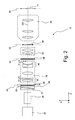
- the FIG. 1 shows in a highly schematic perspective view of a projection exposure apparatus 10, which is suitable for the lithographic production of microstructured components.
- the projection exposure apparatus 10 contains an illumination system 12 for generating a projection light beam, which illuminates a narrow light field 16 on a mask 14 and an annular segment-shaped light field 16 in the exemplary embodiment shown. Structures 18 lying on the mask 14 within the light field 16 are imaged onto a photosensitive layer 22 with the aid of a projection objective 20.
- the photosensitive layer 22, which may be, for example, a photoresist is applied to a wafer 24 or other suitable substrate and is located in the image plane of the projection objective 20. Since the projection objective 20 is generally a magnification ⁇ ⁇ 1, the structures 18 lying within the light field 16 are depicted as being smaller than the area 16 '.
- the mask 14 and the wafer 24 are moved during the projection along a direction designated Y.
- the ratio of the movement speeds is equal to the magnification ⁇ of the projection objective 20. If the projection objective 20 produces an inversion of the image, the movements of the mask 14 and the wafer 22 are in opposite directions, as shown in FIG FIG. 1 is indicated by arrows A1 and A2. In this way, the light field 16 is guided in a scanning movement over the mask 14, so that even larger structured areas can be projected coherently onto the photosensitive layer 22.
- the Y direction is therefore also referred to as scan direction.
- the invention can also be used in the case of projection exposure apparatuses designated as wafer steppers, in which no movement movements take place during the projection.
- the FIG. 2 shows in a simplified and not to scale meridional section details of the illumination system 12.
- the illumination system 12 includes a light source 26, which at least partially generates spatially coherent projection light.
- a light source 26 are lasers, since the light emitted by lasers is spatially and temporally highly coherent.
- the light source 26 is an excimer laser with which light can be generated in the (deep) ultraviolet spectral range.
- the use of short-wave projection light is advantageous because it allows high resolution to be achieved in optical imaging in this way.
- Commonly used are excimer lasers with the laser media KrF, ArF or F 2 , which can be used to generate light with the wavelengths 248 nm, 193 nm and 157 nm, respectively.
- thermal light sources if one removes from the light generated therefrom, e.g. produced by using small apertures, (partially) coherent light beams.
- the light generated by the excimer laser used as the light source 26 is highly concentrated and diverges only slightly. It is therefore first expanded in a beam expander 28.
- the beam expander 28 may, for example, be an adjustable mirror arrangement which increases the dimensions of the approximately rectangular light beam cross section.
- the expanded light beam then passes through an optically birefringent wedge-shaped prism, hereinafter referred to as wedge 32, a compensator element 34 and a diffractive optical element 36.
- wedge 32 an optically birefringent wedge-shaped prism
- compensator element 34 a compensator element 34 and a diffractive optical element 36.
- the diffractive optical element 36 is adjoined by a zoom-axicon module 38, which establishes a Fourier relationship between a field plane 40, in which the diffractive optical element 36 is arranged, and a pupil plane 42.
- a zoom-axicon module 38 which establishes a Fourier relationship between a field plane 40, in which the diffractive optical element 36 is arranged, and a pupil plane 42.
- the zoom axicon assembly 38 includes a zoom lens indicated at 44 and an axicon group 46 which includes two axicon elements with conical and complementary surfaces. With the help of the axicon group 46, the radial light distribution can be changed in order to achieve in this way an annular illumination of the pupil plane 42. By adjusting the zoom lens 44, the diameter of the areas illuminated in the pupil plane 42 can be changed.
- an optical integrator 48 is arranged, which may be, for example, an array of microlens arrays.
- Each microlens forms a secondary one Light source, which generates a divergent light beam with an angle given by the geometry of the microlens angle spectrum.
- the light beams generated by the secondary light sources are superimposed by a condenser 50 in an intermediate field plane 52, whereby it is illuminated very homogeneously.
- a field stop 54 is arranged in the illustrated embodiment, which may comprise a plurality of adjustable cutting edges and / or a plurality of narrow finger-like aperture elements, which are individually inserted into the light path.
- the intermediate field plane 52 is imaged with the aid of a field diaphragm objective 56 onto the object plane 58 of the projection objective 20, in which the mask 14 is arranged.
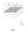
- FIG. 3 shows the diffractive optical element 36 in a perspective view. Underneath, the wedge 32 is indicated by dashed lines in order to illustrate the relative arrangement between the diffractive optical element 36 and the wedge 32.
- the compensator element 34 arranged between them in this exemplary embodiment is not shown for the sake of clarity.
- the diffractive optical element 36 has a substrate 60 which carries at least on one side, here on the side facing away from the wedge 32 side, differently structured regions. In the illustrated embodiment, these areas are periodic Arrangement of strips 62X, 62Y, all of which have the same width w. Each of the strips 62X includes diffractive structures that diffract the light in the X direction, as shown in FIG FIG. 3 for two diffraction orders denoted 64X. The diffraction angles in the ZX plane should be symmetrical with respect to a ZY plane.
- the strips 62Y the same applies to the Y direction, ie they diffract the light exclusively in the YZ plane, which in the FIG. 3 is indicated by two diffraction orders 64Y.
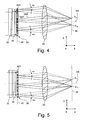
- FIG. 4 shows the wedge 32, the compensator element 34 and the diffractive optical element 36 in a section parallel to the XZ plane.
- the zoom-axicon assembly is indicated here only by a lens 38 ', which produces a Fourier relationship between the field plane 40 and the pupil plane 42.
- all the parallel light rays emanating from the diffractive optical element 36 at the same angle meet at the same point.
- the collimated light passing the stripes 62X diffracts only in the XZ plane by angles + ⁇ x and - ⁇ x , as shown in FIG FIG.
- the rays diffracted by the angle ⁇ x all meet at a point P x in the pupil plane 42 and the rays diffracted by the angle - ⁇ x all converge at a point P -x .
- the pupil plane 42 two points that are the same distance from an optical axis OA of the illumination system 10 and are diametrically opposite each other.
- the strips 62Y which diffract the light exclusively in the YZ plane.
- FIG. 5 which shows the wedge 32, the compensator element 34 and the diffractive optical element 36 in a section parallel to the YZ plane.
- the light rays emanating from the angles ⁇ Y and - ⁇ Y meet at two points P Y and P- Y in the pupil plane 42.
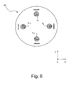
- the light distribution in the pupil plane 42 produced by the diffractive optical element 36 is shown in FIG. It was assumed that the diffraction of the strips 62X, 62Y is determined so as to be formed instead of the points denoted by P X, P X, P Y, and P -Y broader poles.
- the diffraction structures are so small that in the strips 62X, 62Y each region, over the extent of which the change in thickness of the wedge 32 is negligibly small, produces an angular spectrum which in the far field, ie in the pupil plane 42, becomes a pair of poles P X , P -X or P Y , P -Y leads.
- FIG. 7 shows the wedge 32, the compensator element 34 and the diffractive optical element 36 enlarged in a section parallel to the XZ plane.
- falls on the wedge 32 largely collimated, linearly polarized and highly spatially coherent laser light.
- Two rays of the incident on the wedge 32 light beam are in the FIG. 7 denoted 70, 72.
- the linear polarization direction of the laser light within the XY plane is indicated by double arrows 74, the double arrows 74 are thus "folded up" by 90 °.
- the wedge 32 is made of a birefringent material, for example magnesium fluoride.
- the wedge 32 has a wedge angle ⁇ and an optical birefringence axis which makes an angle of 45 ° to the polarization direction 74 of the incident projection light.
- the upper wedge surface 76 which is inclined by the wedge angle .gamma.
- the light rays 70, 72 are broken as they exit the wedge 32 and are thereby deflected in their direction.
- the compensator element 34 has the task of reversing this distraction.
- the compensator element 34 is therefore likewise wedge-shaped, but the wedge angle may differ from the wedge angle ⁇ of the wedge 34, depending on the refractive index of the compensator element 34.
- the polarization state in the XY plane is indicated after the light has passed through the birefringent wedge 32.
- This representation is also (like the double arrows 74) "folded up" by 90 °.
- the polarization state of a light beam after the passage of the wedge 32 depends on how thick the wedge 32 is at the respective passage location of the light beam. Since the thickness of the wedge 32 changes continuously in the X direction, the polarization state along this direction also changes continuously. Thus, as seen in the X-direction, all the states of polarization occur, as in the FIG. 7 are shown below the diffractive optical element 36. It can also be seen from this representation that the change in the polarization state is periodic with the period p.
- the superimposition of the two photons a, b considered here into linearly polarized light can be mathematically determined by the G1.
- E 1 a and E 1 b are the electric field vectors of the two photons a and b and ⁇ describes the phase and thus the polarization state of the field vectors.
- E p 1 a , E s 1 a , E p 1 b and E s 1 b set here equal to 1
- the real components of the electric field vectors E 1 a and E 1 b are parallel or perpendicular to the optical birefringence axis of the wedge 32 designated.
- ⁇ is the wavelength of the light
- ⁇ n is the amount of the difference between the refractive index n 0 of the ordinary ray and the refractive index n a of the extraordinary ray in the birefringent wedge 32 at the wavelength ⁇ .
- the arrangement of stripes 62X, 62Y is chosen to be within a period of width p completely a strip 62X and a strip 62Y has space.
- the two wedges then have the same wedge angle ⁇ / 2.
- the width w of the strips 62X, 62Y can be halved if both birefringent wedges have the wedge angle ⁇ .
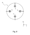
- the diffractive optical element 36 is displaced by half a period p / 2 along the X direction, one obtains in the pupil plane 42 Pole P X , P -X , P Y and P -Y with linearly polarized light in the radial direction, as shown in FIG FIG. 8 is shown.
- FIG. 9 shows in a to the FIG. 3 Similar perspective perspective view of another embodiment of a diffractive optical element, which is here indicated overall with 36 '. Unlike the one in the FIG. 3 In the embodiment shown, the diffractive optical element 32 includes stripes 62 which do not contain diffraction structures. The light passing through the strips 62 therefore remains collimated parallel to the optical axis.
- the non-diffraction patterned stripes 62 are offset by two and a half (generally 2m + 1/2) periods in the illustrated embodiment, light emerging from adjacent unstructured stripes 62 is polarized orthogonal to each other.
- the distance between the unstructured regions 62 is large enough that there is no significant coherence relationship between the photons emerging from the adjacent stripes, an incoherent superposition of orthogonal polarization states in the pupil plane 42 will result, resulting in unpolarized light.
- the light emerging from the strips 62 parallel to the optical axis is focused by the zoom-axicon assembly 38 at a point on the optical axis in the pupil plane 42.
- FIG. 10 shows the resulting pupil plane 42 in one of the FIGS. 6 and 8th ajar representation.
- P c an additional pole, which is designated P c and is penetrated by unpolarized light.
- An alternative way to produce an unpolarized pole is to provide stripes on the diffractive optical element 36, whose width is significantly greater than the spatial coherence cells of the laser light. Then, if the stripe width is exactly a multiple of the period p, then unpolarized light is produced, which is similar to the one already mentioned at the outset US Pat. No. 6,535,273 described finds.
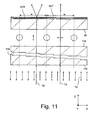
- FIG. 11 shows for another embodiment in one of the FIG. 7 Another way of producing different polarization states is to use a different representation.
- the in the FIG. 11 shown alternative Arrangement comprises a birefringent stepped prism 132, a compensator element 134 and the diffractive optical element 36 of the FIG. 3 ,
- the birefringent prism 132 is designed substantially the same as the wedge 32 in the FIG. 7 shown embodiment.
- the optical birefringence axis also includes an angle of 45 ° to the direction of polarization 74 of the incident projection light.
- the inclined wedge surface 76 which in the in the FIG. 7 however, in the case of the birefringent prism 132, it is replaced by a step surface 176, the steps of which increase along the X direction.
- the birefringent prism 132 thus receives the overall shape of a staircase.
- the compensator element 134 is also formed as a stepped prism, but without being birefringent.
- the compensator element 134 is required only in the event that not only axially parallel rays 70, 72 strike the birefringent prism 132 from below, but also rays which are (slightly) inclined to the optical axis.
- the compensator element 134 then ensures that the directional distribution of the rays passing through the prism 132 and the compensator element 134 remains unchanged.
- the effect of the compensator element 134 corresponds in principle to the effect of the compensator element 34 in FIG FIG. 7 shown Arrangement.
- the compensator element 134 can also have inclined surfaces which are arranged in an inclined manner. In the case of highly paraxial light, the compensator element 134 can be completely eliminated.
- the step surface 176 and thus the distribution of the thickness (dimension along the Z direction) of the birefringent prism 132 along the X direction is set so that incident largely collimated in the Y direction linearly polarized (see "folded" double arrows 74) and highly spatially coherent light is not changed either in its polarization state, the polarization direction is rotated by 90 ° or is converted into right or left circularly polarized light.
- the distribution of the thickness is further set such that each of the strips 62X, 62Y falls light whose polarization state in the X direction changes from circularly polarized to linearly polarized to reverse circularly polarized.
- the pupil plane 42 is linearly polarized along either the Y direction or the X direction.
- each strip 62X, 62Y also be associated with two or more than three different thicknesses.
- each strip 62X, 62Y also be associated with two or more than three different thicknesses.
- thickness tolerances can then compensate each other more easily.
Abstract
Description
Die Erfindung betrifft ein Beleuchtungssystem einer mikrolithographischen Projektionsbelichtungsanlage. Die Erfindung betrifft insbesondere ein Beleuchtungssystem, mit dem sich ein vom Beleuchtungswinkel abhängender Polarisationszustand des auf eine Maske auftreffenden Projektionslichts einstellen läßt.The invention relates to an illumination system of a microlithographic projection exposure apparatus. In particular, the invention relates to a lighting system with which a polarization state, dependent on the illumination angle, of the projection light impinging on a mask can be set.
Integrierte elektrische Schaltkreise und andere mikrostrukturierte Bauelemente werden üblicherweise hergestellt, indem auf ein geeignetes Substrat, bei dem es sich beispielsweise um einen Silizium-Wafer handeln kann, mehrere strukturierte Schichten aufgebracht werden. Zur Strukturierung der Schichten werden diese zunächst mit einem Photolack bedeckt, der für Licht eines bestimmten Wellenlängenbereiches, z.B. Licht im tiefen ultravioletten Spektralbereich (DUV, deep ultraviolet), empfindlich ist. Anschließend wird der so beschichtete Wafer in einer Projektionsbelichtungsanlage belichtet. Dabei wird ein Muster aus beugenden Strukturen, das auf einer Maske angeordnet ist, auf den Photolack mit Hilfe eines Projektionsobjektivs abgebildet. Da der Abbildungsmaßstab dabei im allgemeinen kleiner als 1 ist, werden derartige Projektionsobjektive häufig auch als Reduktionsobjektive bezeichnet.Integrated electrical circuits and other microstructured devices are typically fabricated by applying a plurality of patterned layers to a suitable substrate, which may be a silicon wafer, for example. To structure the layers, they are first covered with a photoresist which is sensitive to light of a specific wavelength range, for example light in the deep ultraviolet spectral range (DUV, deep ultraviolet ). Subsequently, the thus coated wafer is exposed in a projection exposure apparatus. In doing so, a pattern of diffractive structures is placed on a mask is imaged onto the photoresist using a projection lens. Since the magnification is generally less than 1, such projection lenses are often referred to as reduction lenses.
Nach dem Entwickeln des Photolacks wird der Wafer einem Ätzprozeß unterzogen, wodurch die Schicht entsprechend dem Muster auf der Maske strukturiert wird. Der noch verbliebene Photolack wird dann von den verbleibenden Teilen der Schicht entfernt. Dieser Prozeß wird so oft wiederholt, bis alle Schichten auf den Wafer aufgebracht sind.After developing the photoresist, the wafer is subjected to an etching process, whereby the layer is patterned according to the pattern on the mask. The remaining photoresist is then removed from the remaining parts of the layer. This process is repeated until all layers are applied to the wafer.
Die bei der Belichtung verwendeten Projektionsbelichtungsanlagen enthalten ein Beleuchtungssystem, das mit einem Projektionslichtbündel die zu projizierenden Strukturen auf der Maske ausleuchtet. Das Beleuchtungssystem enthält als Lichtquelle im allgemeinen einen Laser, der linear polarisiertes Licht erzeugt. Insbesondere bei der Verwendung sehr kurzwelligen Projektionslichts (z.B. λ = 157 nm) können jedoch bei bestimmten optischen Elementen unerwünschte polarisationsabhängige Effekte auftreten, welche die Abbildungseigenschaften des Projektionsobjektivs stören. Ein Beispiel hierfür ist die intrinsische Doppelbrechung von Kalziumfluorid (CaF2), das bei diesen kurzen Wellenlängen eine deutlich höhere Transparenz als übliche Linsenmaterialien wie etwa Quarzglas aufweist und deswegen diese Materialien teilweise oder sogar ganz ersetzt.The projection exposure apparatus used in the exposure contain a lighting system which uses a projection light beam to illuminate the structures to be projected on the mask. The illumination system generally includes as a light source a laser that produces linearly polarized light. In particular, when using very short-wavelength projection light (eg λ = 157 nm), however, unwanted polarization-dependent effects can occur in certain optical elements, which disturb the imaging properties of the projection lens. An example of this is the intrinsic birefringence of calcium fluoride (CaF 2 ), which at these short wavelengths has a significantly higher transparency than conventional lens materials such as quartz glass and therefore partially or even completely replaces these materials.
Um derartige Polarisationsabhängigkeiten zu verringern, sind bei einigen derartiger Projektionsbelichtungsanlagen zusätzliche Maßnahmen vorgesehen, um das vom Laser erzeugte linear polarisierte Projektionslicht in zirkular polarisiertes Licht oder sogar in unpolarisiertes Licht umzuwandeln, wie dies etwa in der
Andererseits hat sich herausgestellt, daß sich in bestimmten Fällen der Kontrast der Abbildung erhöhen läßt, wenn wenigstens ein Teil des auf die Maske auftreffenden Projektionslichts eine Polarisationsvorzugsrichtung hat, also linear oder elliptisch polarisiert ist. Eine weitere Verbesserung des Kontrasts läßt sich häufig erzielen, wenn der Polarisationszustand von dem Beleuchtungswinkel abhängt, unter dem das Projektionslichtstrahlen auf die Maske treffen.On the other hand, it has been found that in certain cases, the contrast of the image can be increased if at least a portion of the incident on the mask projection light has a polarization preferred direction, that is linear or elliptically polarized. A further improvement of the contrast can often be achieved if the polarization state depends on the illumination angle at which the projection light beams strike the mask.
Die
Aus der internationalen Anmeldung
Aus der
Da das diffraktive optische Element aus einer großen Zahl von Einzelelementen zusammengesetzt ist, entstehen relativ viele Randbereiche, die zur Entstehung von unerwünschtem Streulicht führen. Ferner müssen bei den polarisationsbeeinflussenden Komponenten relativ enge Dickentoleranzen eingehalten werden, was technologisch schwierig ist und deswegen zu hohen Kosten für das diffraktive optische Element führt.Since the diffractive optical element is composed of a large number of individual elements, a relatively large number of edge regions arise, which lead to the formation of unwanted scattered light. Furthermore, in the polarization-influencing components relatively tight thickness tolerances must be met, which is technologically difficult and therefore leads to high costs for the diffractive optical element.
Aus der
Aus der
Vor diesem Hintergrund ist es Aufgabe der Erfindung, ein Beleuchtungssystem einer mikrolithographischen Projektionsbelichtungsanlage anzugeben, mit dem sich der Polarisationszustand des Projektionslichts gezielt in Abhängigkeit vom Beleuchtungswinkel einstellen läßt, unter dem Lichtstrahlen auf die Maske fallen.Against this background, it is an object of the invention to provide an illumination system of a microlithographic projection exposure apparatus specify with which the polarization state of the projection light can be adjusted selectively as a function of the illumination angle, fall under the light rays on the mask.
Gelöst wird diese Aufgabe durch ein Beleuchtungssystem mit einer ersten optischen Anordnung zur Erzeugung eines Lichtbündels, bei dem das Licht wenigstens über einen Teil des Querschnitts des Lichtbündels hinweg unterschiedliche Polarisationszustände hat und räumlich wenigstens teilweise kohärent ist. Ferner ist eine zweite optische Anordnung vorgesehen, die zwischen der ersten optischen Anordnung und einer Pupillenebene angeordnet ist. Die zweite optische Anordnung teilt das Lichtbündel auf wenigsten zwei unterschiedliche Orte in der Pupillenebene auf und überlaqgrt die von der ersten optischen Anordnung erzeugten unterchiedlichen Polarisationszustände zu Pupillenpolarisationszuständen, die an den wenigstens zwei Orten unterschiedlich sind.This object is achieved by an illumination system having a first optical arrangement for generating a light bundle, in which the light has different polarization states over at least part of the cross section of the light bundle and is spatially at least partially coherent. Furthermore, a second optical arrangement is provided, which is arranged between the first optical arrangement and a pupil plane. The second optical arrangement divides the light beam into at least two different locations in the pupil plane and superimposes the different polarization states produced by the first optical arrangement to pupil polarization states that are different at the at least two locations.
Die Erfindung beruht auf der Erkenntnis, daß man durch gezielte Überlagerung kohärenter Lichtanteile mit unterschiedlichen Polarisationszuständen in einer Pupillenebene eine Intensitätsverteilung erzielen kann, bei welcher der Polarisationszustand des Lichts in gewünschter Weise vom Ort abhängt, wodurch sich - bezogen auf die Maskenebene - die gewünschte Abhängigkeit des Polarisationszustands vom Beleuchtungswinkel einstellt.The invention is based on the finding that one can achieve an intensity distribution by deliberately superimposing coherent light components with different polarization states in a pupil plane, in which the polarization state of the light depends on the location in a desired manner, which results in the desired dependence of the mask on the mask plane Polarization state of the illumination angle sets.
Die erste optische Anordnung kann beispielsweise eine thermische Lichtquelle aufweisen, aus deren Licht mit Hilfe einer Lochblende kohärentes, aber unpolarisiertes Licht erzeugt wird. Mit Hilfe von Polarisationsfiltern und ggf. zusätzlichen Verzögerungsplättchen können daraus beispielsweise unterschiedliche lineare, zirkulare oder elliptische Polarisationszustände erzeugt werden, die dann mit Hilfe beugender oder brechender optischer Elemente in der Pupillenebene zu dem gewünschten Polarisationszustand überlagert werden.By way of example, the first optical arrangement may comprise a thermal light source, from the light of which coherent but unpolarized light is generated by means of a pinhole. With the aid of polarization filters and, if appropriate, additional delay plates, it is possible, for example, to generate different linear, circular or elliptical polarization states, which are then superimposed with the aid of diffractive or refractive optical elements in the pupil plane to the desired polarization state.
Bei einem vorteilhaften Ausführungsbeispiel ändern sich die Polarisationszustände des von der ersten Anordnung erzeugten Lichtbündels wenigstens über den Teil des Querschnitts des Lichtbündels hinweg entlang wenigstens einer Richtung kontinuierlich und periodisch. Dadurch besteht die Möglichkeit, durch geeignete Überlagerung in weiten Grenzen beliebige Polarisationszustände in der Pupillenebene einzustellen.In an advantageous embodiment, the polarization states of the light beam generated by the first arrangement change continuously and periodically at least over the part of the cross section of the light beam along at least one direction. This makes it possible to set arbitrary polarization states in the pupil plane by suitable superposition within wide limits.
Besonders einfach läßt sich die erste optische Anordnung realisieren, wenn die Lichtquelle linear polarisiertes und räumlich wenigstens teilweise kohärentes Projektionslicht erzeugt, wie dies etwa bei Lasern der Fall ist. Mit Hilfe eines doppelbrechenden Prismas läßt sich dann der Polarisationszustand eines hindurchtretenden Lichtbündels entlang einer Richtung periodisch verändern. Das Prisma muß lediglich die Eigenschaft haben, das sich seine Dicke nur entlang einer Richtung verändert. Diese Bedingung wird z.B. von einem keilförmigen Prisma erfüllt. Da sich in diesem Fall die Dicke kontinuierlich ändert, verändert sich auch der Polarisationszustand eines hindurchtretenden Lichtbündels entlang dieser Richtung kontinuierlich. Eine ähnliche Wirkung wird erzielt, wenn mehrere Abschnitte, innerhalb derer sich die Dicke kontinuierlich ändert, diskontinuierlich aneinander angrenzen. Ein Beispiel hierfür ist z.B. ein Prisma mit einem sägezahnähnlichen Profil.The first optical arrangement can be realized particularly simply if the light source generates linearly polarized and spatially at least partially coherent projection light, as is the case with lasers, for example. With the aid of a birefringent prism, the polarization state of a light beam passing through can then be periodically changed along one direction. The prism only needs to have the property that its thickness changes only along one direction. This condition is fulfilled eg by a wedge-shaped prism. Since the thickness changes continuously in this case, the state of polarization of a light beam passing therethrough continuously changes along this direction. A similar effect is achieved when several sections, within which the thickness changes continuously, adjoin one another discontinuously. An example of this is, for example, a prism with a sawtooth-like profile.
Bei einem anderen Ausführungsbeispiel hat das Prisma kein kontinuierliches, sondern ein gestuftes Dickenprofil. Falls die Stufen in einer Richtung ansteigen, so erhält das Prisma insgesamt die Form einer Treppe. Ein Prisma mit einem gestuften Dickenprofil verändert den Polarisationszustand eines hindurchtretenden Lichtbündels entlang der Richtung, in der sich die Dicke des Prismas ändert, nicht kontinuierlich, sondern diskontinuierlich. Je mehr Stufen pro Längeneinheit vorgesehen sind, desto weniger wird der durch Überlagerung erhaltene Polarisationszustand von Dickentoleranzen abhängen.In another embodiment, the prism does not have a continuous, but a stepped thickness profile. If the steps increase in one direction, the prism as a whole takes the form of a staircase. A prism having a stepped thickness profile changes the polarization state of a passing light beam along the direction in which the thickness of the prism changes not continuously but discontinuously. The more steps per unit length are provided, the less will the polarization state obtained by superposition depend on thickness tolerances.
Hat das Prisma eine optische Doppelbrechungsachse, die einen Winkel von 45° zu einer Polarisationsrichtung des linear polarisierten Projektionslichts einschließt, so lassen sich alle denkbaren Polarisationszustände erzeugen. Dies wiederum ist Voraussetzung dafür, daß man auch in der Pupillenebene alle denkbaren Polarisationszustände durch geeignete Überlagerung kohärenter unterschiedlich polarisierter Lichtanteile erreichen kann.If the prism has an optical birefringence axis which encloses an angle of 45 ° to a polarization direction of the linearly polarized projection light, then all conceivable polarization states can be generated. This, in turn, is a prerequisite for ensuring that all conceivable polarization states are also present at the pupil level can be achieved by suitable superimposition of coherent differently polarized light components.
Bei einer vorteilhaften Ausgestaltung weist die zweite Anordnung ein diffraktives optisches Element auf, das lokal variierende Beugungseigenschaften hat. Die Verwendung diffraktiver optischer Elemente ist insofern günstig, weil sich damit praktisch beliebige Winkelverteilungen erzeugen lassen. Der von dem diffraktiven optischen Element erzeugten Winkelverteilung entspricht im Fernfeld eine Intensitätsverteilung in der Pupillenebene.In an advantageous embodiment, the second arrangement has a diffractive optical element which has locally varying diffraction properties. The use of diffractive optical elements is advantageous in that it allows practically any angular distributions to be generated. The angular distribution generated by the diffractive optical element corresponds to an intensity distribution in the pupil plane in the far field.
Weist das diffraktive optische Element mindestens zwei parallel zueinander angeordnete Streifen mit unterschiedlichen Beugungseigenschaften auf, so lassen sich, insbesondere im Zusammenwirken mit einem doppelbrechenden Prisma, zwei Orte oder Bereiche mit unterschiedlichen Polarisationszuständen in der Pupillenebene ausleuchten.If the diffractive optical element has at least two strips with different diffraction properties arranged parallel to one another, then, in particular in cooperation with a birefringent prism, two locations or areas with different polarization states in the pupil plane can be illuminated.
Weitere Merkmale und Vorteile der Erfindung ergeben sich aus der nachfolgenden Beschreibung von Ausführungsbeispielen anhand der Zeichnungen. Darin zeigen:
- Figur
- 1 eine Projektionsbelichtungsanlage in stark schematisierter perspektivischer Darstellung;
- Figur 2
- ein erfindungsgemäßes Beleuchtungssystem in einem vereinfachten Meridionalschnitt;
- Figur 3
- ein diffraktives optisches Element mit streifenförmigen Beugungsbereichen in einer perspektivischen Darstellung;
- Figur 4
- einen vergrößerten Ausschnitt aus der
Figur 2 in einem X-Z-Schnitt; - Figur 5
- einen vergrößerten Ausschnitt aus der
Figur 2 in einem Y-Z-Schnitt; - Figur 6
- die sich in der Pupillenebene des in der
Figur 2 gezeigten Beleuchtungssystems einstellende Intensitäts- und Polarisationsverteilung; - Figur 7
- eine Anordnung eines doppelbrechenden Keils und des in der
Figur 3 gezeigten diffraktiven optischen Elements in einem X-Z-Schnitt; - Figur 8
- die sich in der Pupillenebene eines Beleuchtungssystems gemäß einem anderen Ausführungsbeispiels einstellende Intensitäts- und Polarisationsverteilung;
- Figur 9
- eine an die
Figur 3 angelehnte Darstellung eines diffraktiven optischen Elements gemäß einem weiteren Ausführungsbeispiel; Figur 10- die mit dem in der
Figur 9 gezeigten diffraktiven optischen Element erhaltene Intensitäts-und Polarisationsverteilung in der Pupillenebene in einer an dieFiguren 6 und8 angelehnten Darstellung; - Figur 11
- eine an die
Figur 7 angelehnte Darstellung einer Anordnung eines treppenförmigen Prismas und des in derFigur 3 gezeigten diffraktiven optischen Elements in einem X-Z-Schnitt.
- figure
- 1 a projection exposure apparatus in a highly schematic perspective view;
- FIG. 2
- an inventive illumination system in a simplified meridional section;
- FIG. 3
- a diffractive optical element with strip-shaped diffraction areas in a perspective view;
- FIG. 4
- an enlarged section of the
FIG. 2 in an XZ section; - FIG. 5
- an enlarged section of the
FIG. 2 in a YZ-section; - FIG. 6
- in the pupil plane of the
FIG. 2 shown illumination system adjusting intensity and polarization distribution; - FIG. 7
- an arrangement of a birefringent wedge and in the
FIG. 3 shown diffractive optical element in an XZ section; - FIG. 8
- the intensity and polarization distribution occurring in the pupil plane of an illumination system according to another embodiment;
- FIG. 9
- one to the
FIG. 3 ajar representation of a diffractive optical element according to another embodiment; - FIG. 10
- with the in the
FIG. 9 shown diffraction optical element obtained intensity and polarization distribution in the pupil plane in one of theFIGS. 6 and8th ajar representation; - FIG. 11
- one to the
FIG. 7 ajar representation of an arrangement of a staircase prism and in theFIG. 3 shown diffractive optical element in an XZ section.
Die
Bei der dargestellten Projektionsbelichtungsanlage 10 werden die Maske 14 und der Wafer 24 während der Projektion entlang einer mit Y bezeichneten Richtung verfahren. Das Verhältnis der Verfahrgeschwindigkeiten ist dabei gleich dem Abbildungsmaßstab β des Projektionsobjektivs 20. Falls das Projektionsobjektiv 20 eine Invertierung des Bildes erzeugt, verlaufen die Verfahrbewegungen der Maske 14 und des Wafers 22 gegenläufig, wie dies in der
Die
Zumindest prinzipiell geeignet sind aber auch thermische Lichtquellen, wenn man aus dem davon erzeugten Licht, z.B. durch Verwendung kleiner Blendenöffnungen, (partiell) kohärente Lichtbündel erzeugt.However, at least in principle also suitable are thermal light sources, if one removes from the light generated therefrom, e.g. produced by using small apertures, (partially) coherent light beams.
Das von dem als Lichtquelle 26 verwendeten Excimer-Laser erzeugte Licht ist stark gebündelt und divergiert nur schwach. Es wird deswegen zunächst in einem Strahlaufweiter 28 aufgeweitet. Bei dem Strahlaufweiter 28 kann es sich zum Beispiel um eine verstellbare Spiegelanordnung handeln, welche die Abmessungen des annähernd rechteckigen Lichtbündelquerschnitts vergrößert.The light generated by the excimer laser used as the
Das aufgeweitete Lichtbündel durchtritt anschließend ein optisch doppelbrechendes keilförmiges Prisma, das im folgenden kurz als Keil 32 bezeichnet wird, ein Kompensatorelement 34 und ein diffraktives optisches Element 36. Mit Hilfe dieser optischen Elemente, die ausführlich weiter unten mit Bezug auf die
An das diffraktive optische Element 36 schließt sich eine Zoom-Axikon-Baugruppe 38 an, die zwischen einer Feldebene 40, in der das diffraktive optische Element 36 angeordnet ist, und einer Pupillenebene 42 eine Fourier-Beziehung herstellt. Dadurch treffen sich alle unter dem gleichen Winkel von der Feldebene 40 ausgehenden Lichtstrahlen in der Pupillenebene 42 im gleichen Punkt, während alle von einem bestimmten Punkt in der Feldebene 40 ausgehenden Lichtstrahlen die Pupillenebene 42 unter dem gleichen Winkel durchsetzen.The diffractive
Die Zoom-Axikon-Baugruppe 38 enthält ein mit 44 angedeutetes Zoom-Objektiv sowie eine Axicon-Gruppe 46, welche zwei Axicon-Elemente mit konischen und zueinander komplementären Flächen enthält. Mit Hilfe der Axicon-Gruppe 46 läßt sich die radiale Lichtverteilung verändern, um auf diese Weise eine ringförmige Ausleuchtung der Pupillenebene 42 zu erzielen. Durch Verstellung des Zoom-Objektivs 44 lassen sich die Durchmesser der in der Pupillenebene 42 ausgeleuchteten Bereiche verändern.The
In oder in unmittelbarer Nähe der Pupillenebene 42 ist ein optischer Integrator 48 angeordnet, bei dem es sich zum Beispiel um eine Anordnung von Mikrolinsen-Arrays handeln kann. Jede Mikrolinse bildet eine sekundäre Lichtquelle, die ein divergentes Lichtbündel mit einem durch die Geometrie der Mikrolinse vorgegebenen Winkelspektrum erzeugt. Die von den sekundären Lichtquellen erzeugten Lichtbündel werden durch einen Kondensor 50 in einer Zwischenfeldebene 52 überlagert, wodurch diese sehr homogen ausgeleuchtet wird.In or in the immediate vicinity of the
In der Zwischenfeldebene 52 ist bei dem dargestellten Ausführungsbeispiel eine Feldblende 54 angeordnet, die mehrere verstellbare Schneiden und/oder eine Vielzahl schmaler fingerartiger Blendenelemente umfassen kann, die einzeln in den Lichtweg einführbar sind. Die Zwischenfeldebene 52 wird mit Hilfe eines Feldblendenobjektivs 56 auf die Objektebene 58 des Projektionsobjektivs 20 abgebildet, in welcher die Maske 14 angeordnet ist.In the
Die
Das diffraktive optische Element 36 weist ein Substrat 60 auf, das zumindest auf einer Seite, hier auf der von dem Keil 32 abgewandten Seite, unterschiedlich strukturierte Bereiche trägt. Bei dem dargestellten Ausführungsbeispiel handelt es sich bei diesen Bereichen um eine periodische Anordnung von Streifen 62X, 62Y, die alle die gleiche Breite w haben. Jeder der Streifen 62X enthält Beugungsstrukturen, welche das Licht in X-Richtung beugen, wie dies in der
Für die Streifen 62Y gilt entsprechendes für die Y-Richtung, d.h. sie beugen das Licht ausschließlich in der Y-Z-Ebene, was in der
Die
Entsprechendes gilt auch für die Streifen 62Y, welche das Licht ausschließlich in der Y-Z-Ebene beugen. Dies ist in der
Die durch das diffraktive optische Element 36 erzeugte Lichtverteilung in der Pupillenebene 42 ist in der Figur 6 gezeigt. Hierbei wurde angenommen, daß die Beugung der Streifen 62X, 62Y so bestimmt wurde, daß sich anstelle von Punkten die mit PX, P-X, PY und P-Y bezeichneten ausgedehnteren Pole ausbilden. Die Beugungsstrukturen sind dabei so klein, daß in den Streifen 62X, 62Y jeder Bereich, über dessen Ausdehnung hinweg die Dickenänderung des Keils 32 vernachlässigbar klein ist, ein Winkelspektrum erzeugt, das im Fernfeld, d.h. in der Pupillenebene 42, zu einem Paar von Polen PX, P-X bzw. PY, P-Y führt.The light distribution in the
Die
Der Keil 32 besteht aus einem doppelbrechenden Material, zum Beispiel Magnesiumfluorid. Der Keil 32 hat einen Keilwinkel γ und eine optische Doppelbrechungsachse, die einen Winkel von 45° zur Polarisationsrichtung 74 des auftreffenden Projektionslichts einschließt. Infolge der um den Keilwinkel γ geneigt angeordneten oberen Keilfläche 76 werden die Lichtstrahlen 70, 72 beim Austritt aus dem Keil 32 gebrochen und dadurch in ihrer Richtung abgelenkt. Das Kompensatorelement 34 hat die Aufgabe, diese Ablenkung wieder rückgängig zu machen. Das Kompensatorelement 34 ist deswegen ebenfalls keilförmig, jedoch kann der Keilwinkel je nach Brechzahl des Kompensatorelements 34 von dem Keilwinkel γ des Keils 34 verschieden sein.The
Zwischen dem Kompensatorelement 34 und dem diffraktiven optischen Element 36 ist der Polarisationszustand in der X-Y-Ebene angedeutet, nachdem das Licht den doppelbrechenden Keil 32 durchtreten hat. Diese Darstellung ist ebenfalls (wie die Doppelpfeile 74) um 90° "hochgeklappt". Der Polarisationszustand eines Lichtstrahls nach dem Durchtritt des Keils 32 hängt davon ab, wie dick der Keil 32 am jeweiligen Durchtrittsort des Lichtstrahls ist. Da sich die Dicke des Keils 32 kontinuierlich in X-Richtung verändert, ändert sich auch der Polarisationszustand entlang dieser Richtung kontinuierlich. Es treten somit über die X-Richtung gesehen alle Polarisationszustände auf, wie sie in der
Im folgenden wird angenommen, daß innerhalb einer Streifenbreite w das Projektionslicht räumlich und zeitlich vollständig kohärent ist. Bei einem typischen Excimer-Laser liegt nach der Strahlaufweitung in dem Strahlaufweiter 28 die räumlich Kohärenz typischerweise in der Größenordnung von etwa 1 bis 2 mm. Die Annahme vollständiger Kohärenz ist somit bei Streifenbreiten w von weniger als 0,5 mm, besser noch von weniger als 0,25 mm, annähernd erfüllt.In the following it is assumed that within a stripe width w, the projection light is completely coherent spatially and temporally. For a typical excimer laser, after beam expansion in
Im folgenden wird ferner angenommen, daß zwei räumlich und zeitlich kohärente Photonen a und b einen der Streifen 62X durchtreten. Haben die beiden Photonen a, b eine im Vorzeichen entgegengesetzte Phase und gleiche Intensitäten nach dem Durchtritt durch den Keil 32, so überlagern sich die Photonen a, b in der Pupillenebene 42 zu linear polarisiertem Licht. Ausgenutzt wird dabei die Tatsache, daß durch die Zoom-Axikon-Baugruppe 38 eine Überlagerung der unter gleichem Winkel gebeugten Lichtstrahlen in einem Punkt stattfindet, wie dies oben mit Bezug auf die
Die Überlagerung der hier betrachteten zwei Photonen a, b zu linear polarisiertem Licht läßt sich mathematisch durch die G1. (1) beschreiben: 
Die Addition der beiden Photonen a, b in der Pupillenebene 42 liefert somit gemäß G1. (2) linear polarisiertes Licht, dessen Polarisationsrichtung jedoch um den Winkel ![]()
![]()
Da sich aber in der Pupillenebene alle unter dem gleichen Winkel gebeugte Photonen in einem Punkt treffen, kommt es zu einer Überlagerung aller Photonen, die einen Streifen 62X der Breite w durchtreten. Wegen der Beziehung p = 2w liegen die Phasen µ der Photonen in einem Bereich zwischen - n/2 und + π/2. Mathematisch läßt sich die Überlagerung beschreiben als 
Die Überlagerung aller den Streifen 62X durchtretenden Photonen mit Polarisationszuständen zwischen links und rechts zirkular polarisiert ergibt also linear polarisiertes Licht, dessen Polarisationsrichtung hier parallel zur Polarisationsrichtung 74 ist, die das Licht vor dem Durchtritt durch den Keil 32 hatte.The superimposition of all the photons passing through the
Entsprechende Überlegungen gelten auch für die Streifen 62Y, nur daß dort durch die Überlagerung linear polarisiertes Licht entsteht, dessen Polarisationsrichtung um 90° gegenüber der ursprünglichen Polarisationsrichtung 74 verdreht ist. Die sich durch die Überlagerung ergebenden linearen Polarisationsrichtungen sind in der
Infolge der vorstehend beschriebenen Überlagerung haben die beiden um 90° zueinander verdrehten Paare von Polen PX, P-X einerseits und PY und P-Y andererseits um 90° zueinander verdrehte Polarisationszustände, wie dies in der
Damit bei dem vorstehend beschriebenen Ausführungsbeispiel der Keil 32 die gewünschten Polarisationszustände erzeugt, muß folgender Zusammenhang zwischen der Periode p = 2w und dem Keilwinkel γ gegeben sein: 
Selbstverständlich ist es möglich, anstelle des Kompensatorelements 34 einen weiteren doppelbrechenden Keil zu verwenden. Gegenüber dem in
Sollen in den Polen PX, P-X, PY und P-Y andere, zum Beispiel elliptische, Polarisationszustände eingestellt werden, so genügt es, das diffraktive optische Element 36 relativ zu dem Keil 32 entlang der X-Richtung zu verschieben. Das diffraktive optische Element bildet dann, zusammen mit einer geeigneten, in der
Grundsätzlich ist es auch möglich, mehr als zwei unterschiedliche Arten unterschiedlich beugender Streifen vorzusehen, wobei auch die Anordnung dieser Streifen nicht unbedingt äquidistant sein muß. Dies ermöglicht die Einstellung von partiell polarisierten Polen in der Pupillenebene 42.In principle, it is also possible to provide more than two different types of differently diffractive strips, wherein the arrangement of these strips not must be absolutely equidistant. This allows the setting of partially polarized poles in the
Die
Auch in diesem Ausführungsbeispiel haben alle Streifen 62, 62X und 62Y die gleiche Streifenbreite w = p/2. Da die nicht mit Beugungsstrukturen versehenen Streifen 62 jedoch bei dem dargestellten Ausführungsbeispiel um zweieinhalb (allgemein 2m+1/2) Perioden zueinander versetzt angeordnet sind, ist das aus benachbarten unstrukturierten Streifen 62 austretende Licht orthogonal zueinander polarisiert. Ist der Abstand zwischen den unstrukturierten Bereichen 62 ferner groß genug, daß keine nennenswerte Kohärenzbeziehung mehr zwischen den aus den benachbarten Streifen austretenden Photonen besteht, so kommt es zu einer inkohärenten Überlagerung orthogonaler Polarisationszustände in der Pupillenebene 42, was zu unpolarisiertem Licht führt.Also in this embodiment, all strips 62, 62X and 62Y have the same strip width w = p / 2. However, since the non-diffraction
Da in den Streifen 62 keine Beugung stattfindet, wird das parallel zur optischen Achse aus den Streifen 62 austretende Licht durch die Zoom-Axikon-Baugruppe 38 in einem auf der optischen Achse liegenden Punkt in der Pupillenebene 42 fokussiert.Since no diffraction occurs in the
Soll in der Pupillenebene 42 ein zentraler ausgedehnterer Pol mit unpolarisiertem Licht ausgeleuchtet werden, so können in den Bereichen 62 schwach beugende Strukturen vorgesehen sein, die das Licht nur um relativ kleine Winkel ablenken. Die
Eine alternative Möglichkeit zur Erzeugung eines unpolarisierten Pols besteht darin, Streifen auf dem diffraktiven optischen Element 36 vorzusehen, deren Breite deutlich größer ist als die räumlichen Kohärenzzellen des Laserlichts. Beträgt dann die Streifenbreite genau einem Vielfachen der Periode p, so entsteht unpolarisiertes Licht, wie man dies ähnlich auch in der eingangs bereits erwähnten
Die
Das doppelbrechende Prisma 132 ist im wesentlichen genauso ausgelegt wird der Keil 32 bei dem in der
Das Kompensatorelement 134 ist ebenfalls als treppenförmiges Prisma ausgebildet, ohne jedoch doppelbrechend zu sein. Benötigt wird das Kompensatorelement 134 nur für den Fall, daß nicht nur achsparallele Strahlen 70, 72 von unten auf das doppelbrechende Prisma 132 treffen, sondern auch Strahlen, die zur optischen Achse (geringfügig) geneigt sind. Das Kompensatorelement 134 gewährleistet dann, daß die Richtungsverteilung der durch das Prisma 132 und das Kompensatorelement 134 hindurchtretenden Strahlen unverändert bleibt. Die Wirkung des Kompensatorelements 134 entspricht insoweit prinzipiell der Wirkung des Kompensatorelements 34 der in der
Die Stufenfläche 176 und damit die Verteilung der Dicke (Abmessung entlang der Z-Richtung) des doppelbrechenden Prismas 132 entlang der X-Richtung ist so festgelegt, daß auftreffendes weitgehend kollimiertes, in Y-Richtung linear polarisiertes (siehe "hochgeklappte" Doppelpfeile 74) und hochgradig räumlich kohärentes Licht entweder in seinem Polarisationszustand nicht verrändert wird, die Polarisationsrichtung um 90° gedreht wird oder in rechts oder links zirkular polarisiertes Licht umgewandelt wird.The
In dem dargestellten Ausführungsbeispiel ist die Verteilung der Dicke ferner so festgelegt, daß auf die Streifen 62X, 62Y jeweils Licht fällt, dessen Polarisationszustand in X-Richtung sich von zirkular polarisiert zu linear polarisiert zu umgekehrt zirkular polarisiert ändert. Diese Abfolge von Polarisationszuständen ist auch hier periodisch mit der Periode p, wobei ebenfalls p = 2w gilt.In the illustrated embodiment, the distribution of the thickness is further set such that each of the
Wie man anhand der
Selbstverständlich kann die Stufenfläche 176 auch anders ausgelegt sein. So können z.B. jedem Streifen 62X, 62Y auch zwei oder mehr als drei unterschiedliche Dicken zugeordnet sein. In Betracht kommt beispielsweise, zwei Dicken vorzusehen, die linear polarisiertes Licht in entgegengesetzt elliptisch polarisiertes Licht umwandeln. Damit der an den Überlagerungspunkten entstehende Polarisationszustand möglichst unempfindlich gegen Dickentoleranzen des doppelbrechenden Prismas 132 ist, wird es jedoch im allgemeinen günstiger sein, wenn jeder Zone 62X, 62Y eher mehr als weniger unterschiedliche Dicken zugeordnet sind. Je mehr unterschiedliche Polarisationszustände sich nämlich überlagern, desto weniger fällt es ins Gewicht, wenn eine einzelne Dicke nicht dem spezifizierten Wert entspricht. Ferner können sich Dickentoleranzen dann auch leichter gegenseitig ausgleichen.Of course, the
Claims (20)
- Illumination system (12) of a microlithographic projection exposure apparatus (10), comprising:a) a first optical arrangement (26, 32; 132) for generating a light beam in which, at least over a part of the cross section of the light beam, the light- has different polarisation states and- is at least partially spatially coherent,b) a pupil plane (42), and comprisingc) a second optical arrangement (36, 38),- which is arranged between the first optical arrangement (26, 32; 132) and the pupil plane (42) and- which splits the light beam onto at least two different positions (PX, P-X, PY, P-Y) in the pupil plane (42) while superposing the different polarisation states generated by the first optical arrangement to form pupil polarisation states which are different at the at least two positions (PX, P-X, PY, P-Y).
- Illumination system according to Claim 1, wherein the polarisation states of the light beam which is generated by the first optical arrangement (26, 32; 132) change continuously and periodically along at least one direction (X) at least over the part of the cross section of the light beam.
- Illumination system according to Claim 2, wherein the first arrangement comprises:a) a light source (26) for generating linearly polarised and at least partially spatially coherent projection light andb) a birefringent prism (32; 132) which periodically modifies the polarisation state of a light beam passing through along one direction (X).
- Illumination system according to Claim 3, wherein the prism (32) is wedge-shaped and continuously modifies the polarisation state of a light beam passing through along the direction (X).
- Illumination system according to Claim 3, wherein the prism (132) has a stepped thickness profile and discontinuously modifies the polarisation state of a light beam passing through along the direction (X).
- Illumination system according to one of Claims 3 to 5, wherein the prism (32; 132) has an optical birefringence axis which makes an angle of 45° with a polarisation direction of the linearly polarised projection light.
- Illumination system according to one of the preceding claims, wherein the second arrangement (38) comprises a diffractive optical element (36) which has locally varying diffraction properties.
- Illumination system according to Claim 7, wherein the diffractive optical element (36) comprises at least two strips (62X, 62Y) that are arranged mutually parallel and have different diffraction properties.
- Illumination system according to Claim 8, wherein the diffraction properties of the strips (62X, 62Y) change periodically.
- Illumination system according to Claim 4 and according to one of Claims 8 or 9, wherein the strips (62X, 62Y) are arranged parallel to a direction (Y), which extends perpendicularly to an optical axis (OA) of the illumination system (12) and perpendicularly to a direction along which the thickness of the prism (32; 132) varies.
- Illumination system according to one of Claims 8 to 10, wherein first strips (62X) diffract the light in a plurality of directions in an X-Z plane and second strips (62Y) diffract the light in a plurality of directions in a Y-Z plane.
- Illumination system according to Claim 11, wherein the first strips (62X) generate a dipole distribution in the X direction in the far-field and the second strips (62Y) generate a dipole distribution in the Y direction in the far-field.
- Illumination system according to one of Claims 8 to 12, wherein the width of the strips (62X, 62Y) is selected so that the light passing through an individual strip (62X, 62Y) has a preferential polarisation direction when superposed on one of the at least two positions (PX, P-X, PY, P-Y).
- Illumination system according to Claim 13, wherein the width (w) of the strips (62X, 62Y) is equal to a half of the period with which the polarisation state of the light beam passing through varies periodically.
- Illumination system according to one of Claims 8 to 14, wherein the width (w) of the strips (62X, 62Y) is selected so that the light passing through an individual strip (62X, 62Y) is at least substantially polarised linearly when superposed on one of the at least two positions (PX, P-X, PY, P-Y).
- Illumination system according to one of Claims 8 to 15, wherein the strips (62X, 62Y) have a width (w) which is so small that the light passing through a strip (62X, 62Y) is spatially coherent.
- Illumination system according to one of the preceding claims, comprising an excimer laser as the light source (26).
- Illumination system according to Claim 16 and according to Claim 18, wherein the strips (62X, 62Y) have a width (w) which is less than 0.5 mm.
- Illumination system according to Claim 18, wherein the strips (62X, 62Y) have a width (w) which is less than 0.25 mm.
- Method for producing microstructured components, comprising the following steps:a) providing a microlithographic projection exposure apparatus (10) comprising an illumination system (12) according to one of the preceding claims;b) illuminating a mask (14) with the illumination system (12),c) projecting the illuminated mask (14) onto a photosensitive layer (22).
Applications Claiming Priority (2)
| Application Number | Priority Date | Filing Date | Title |
|---|---|---|---|
| DE102006032878A DE102006032878A1 (en) | 2006-07-15 | 2006-07-15 | Illumination system of a microlithographic projection exposure apparatus |
| PCT/EP2007/005943 WO2008009353A1 (en) | 2006-07-15 | 2007-07-05 | Illumination system of a microlithographic projection exposure apparatus |
Publications (2)
| Publication Number | Publication Date |
|---|---|
| EP2041625A1 EP2041625A1 (en) | 2009-04-01 |
| EP2041625B1 true EP2041625B1 (en) | 2012-06-27 |
Family
ID=38536021
Family Applications (1)
| Application Number | Title | Priority Date | Filing Date |
|---|---|---|---|
| EP07765066A Expired - Fee Related EP2041625B1 (en) | 2006-07-15 | 2007-07-05 | Illumination system of a microlithographic projection exposure apparatus |
Country Status (5)
| Country | Link |
|---|---|
| US (1) | US20090115991A1 (en) |
| EP (1) | EP2041625B1 (en) |
| JP (1) | JP5369319B2 (en) |
| DE (1) | DE102006032878A1 (en) |
| WO (1) | WO2008009353A1 (en) |
Families Citing this family (4)
| Publication number | Priority date | Publication date | Assignee | Title |
|---|---|---|---|---|
| DE102008009601A1 (en) * | 2008-02-15 | 2009-08-20 | Carl Zeiss Smt Ag | Optical system for a microlithographic projection exposure apparatus and microlithographic exposure method |
| US9116303B2 (en) * | 2010-03-05 | 2015-08-25 | Canon Kabushiki Kaisha | Hologram with cells to control phase in two polarization directions and exposure apparatus |
| CN103154818B (en) * | 2010-09-28 | 2015-07-15 | 卡尔蔡司Smt有限责任公司 | Optical system of a microlithographic projection exposure apparatus and method of reducing image placement errors |
| DE102011085334A1 (en) * | 2011-10-27 | 2013-05-02 | Carl Zeiss Smt Gmbh | Optical system in a lighting device of a microlithographic projection exposure apparatus |
Citations (1)
| Publication number | Priority date | Publication date | Assignee | Title |
|---|---|---|---|---|
| US20060055834A1 (en) * | 2002-12-03 | 2006-03-16 | Nikon Corporation | Illumination optical system, exposure apparatus, and exposure method |
Family Cites Families (23)
| Publication number | Priority date | Publication date | Assignee | Title |
|---|---|---|---|---|
| EP0967524A3 (en) * | 1990-11-15 | 2000-01-05 | Nikon Corporation | Projection exposure method and apparatus |
| US5459000A (en) * | 1992-10-14 | 1995-10-17 | Canon Kabushiki Kaisha | Image projection method and device manufacturing method using the image projection method |
| JP3985346B2 (en) * | 1998-06-12 | 2007-10-03 | 株式会社ニコン | Projection exposure apparatus, projection exposure apparatus adjustment method, and projection exposure method |
| DE19829612A1 (en) * | 1998-07-02 | 2000-01-05 | Zeiss Carl Fa | Microlithography lighting system with depolarizer |
| US6563567B1 (en) * | 1998-12-17 | 2003-05-13 | Nikon Corporation | Method and apparatus for illuminating a surface using a projection imaging apparatus |
| JP3927753B2 (en) * | 2000-03-31 | 2007-06-13 | キヤノン株式会社 | Exposure apparatus and device manufacturing method |
| DE10124474A1 (en) * | 2001-05-19 | 2002-11-21 | Zeiss Carl | Microlithographic exposure involves compensating path difference by controlled variation of first and/or second optical paths; image plane difference is essentially independent of incident angle |
| JP2003090978A (en) * | 2001-09-17 | 2003-03-28 | Canon Inc | Illumination device, exposure device and method for manufacturing device |
| EP1367446A1 (en) * | 2002-05-31 | 2003-12-03 | ASML Netherlands B.V. | Lithographic apparatus |
| AU2003255441A1 (en) * | 2003-08-14 | 2005-03-29 | Carl Zeiss Smt Ag | Illuminating device for a microlithographic projection illumination system |
| US7408616B2 (en) * | 2003-09-26 | 2008-08-05 | Carl Zeiss Smt Ag | Microlithographic exposure method as well as a projection exposure system for carrying out the method |
| TWI474132B (en) * | 2003-10-28 | 2015-02-21 | 尼康股份有限公司 | Optical illumination device, projection exposure device, exposure method and device manufacturing method |
| WO2005050325A1 (en) * | 2003-11-05 | 2005-06-02 | Carl Zeiss Smt Ag | Polarization-optimizing illumination system |
| TWI612338B (en) * | 2003-11-20 | 2018-01-21 | 尼康股份有限公司 | Optical illuminating apparatus, exposure device, exposure method, and device manufacturing method |
| JP4497968B2 (en) * | 2004-03-18 | 2010-07-07 | キヤノン株式会社 | Illumination apparatus, exposure apparatus, and device manufacturing method |
| US7324280B2 (en) * | 2004-05-25 | 2008-01-29 | Asml Holding N.V. | Apparatus for providing a pattern of polarization |
| JP2006005319A (en) * | 2004-06-21 | 2006-01-05 | Canon Inc | System and method of lighting optical system, exposure apparatus, and device manufacturing method |
| US7548370B2 (en) * | 2004-06-29 | 2009-06-16 | Asml Holding N.V. | Layered structure for a tile wave plate assembly |
| JP2006196715A (en) * | 2005-01-13 | 2006-07-27 | Nikon Corp | Luminous-flux converting element, illuminating optical apparatus, exposure apparatus, and exposure method |
| JP2006269462A (en) * | 2005-03-22 | 2006-10-05 | Sony Corp | Exposure apparatus and illuminating apparatus |
| US7317512B2 (en) * | 2005-07-11 | 2008-01-08 | Asml Netherlands B.V. | Different polarization in cross-section of a radiation beam in a lithographic apparatus and device manufacturing method |
| US20070058151A1 (en) * | 2005-09-13 | 2007-03-15 | Asml Netherlands B.V. | Optical element for use in lithography apparatus and method of conditioning radiation beam |
| US7525642B2 (en) * | 2006-02-23 | 2009-04-28 | Asml Netherlands B.V. | Lithographic apparatus and device manufacturing method |
-
2006
- 2006-07-15 DE DE102006032878A patent/DE102006032878A1/en not_active Withdrawn
-
2007
- 2007-07-05 WO PCT/EP2007/005943 patent/WO2008009353A1/en active Application Filing
- 2007-07-05 JP JP2009518757A patent/JP5369319B2/en not_active Expired - Fee Related
- 2007-07-05 EP EP07765066A patent/EP2041625B1/en not_active Expired - Fee Related
-
2008
- 2008-11-17 US US12/272,297 patent/US20090115991A1/en not_active Abandoned
Patent Citations (1)
| Publication number | Priority date | Publication date | Assignee | Title |
|---|---|---|---|---|
| US20060055834A1 (en) * | 2002-12-03 | 2006-03-16 | Nikon Corporation | Illumination optical system, exposure apparatus, and exposure method |
Also Published As
| Publication number | Publication date |
|---|---|
| EP2041625A1 (en) | 2009-04-01 |
| WO2008009353A1 (en) | 2008-01-24 |
| DE102006032878A1 (en) | 2008-01-17 |
| US20090115991A1 (en) | 2009-05-07 |
| JP5369319B2 (en) | 2013-12-18 |
| JP2009544146A (en) | 2009-12-10 |
Similar Documents
| Publication | Publication Date | Title |
|---|---|---|
| WO2005017620A2 (en) | Illumination device and polariser for a microlithographic projection exposure installation | |
| WO2006021540A2 (en) | Optical system, i.e. lens or illumination device of a microlithographic projection exposure apparatus | |
| WO2005085955A2 (en) | Transmission filter device | |
| WO2005059653A2 (en) | Polarization optically effective delay system for a microlithographic projection illumination device | |
| DE102006032810A1 (en) | Illumination optics for a microlithography projection exposure apparatus, illumination system with such an illumination optics, microlithography projection exposure apparatus with such an illumination system, microlithographic production method for components and component produced by this method | |
| DE10123725A1 (en) | Objective for microlithographic projection, includes lens element with axis perpendicular to specified fluoride crystal plane | |
| DE10010131A1 (en) | Microlithography projection exposure with tangential polarization involves using light with preferred direction of polarization oriented perpendicularly with respect to plane of incidence | |
| DE10124474A1 (en) | Microlithographic exposure involves compensating path difference by controlled variation of first and/or second optical paths; image plane difference is essentially independent of incident angle | |
| DE10344010A1 (en) | Honeycomb condenser and lighting system with it | |
| DE102010029339A1 (en) | Optical system for a microlithographic projection exposure apparatus and microlithographic exposure method | |
| DE102007042047A1 (en) | Subsystem of a lighting device of a microlithographic projection exposure apparatus | |
| DE102007010650A1 (en) | Lighting device for use with micro lithographic projection exposure system, has micro lens array arranged in light direction of propagation before light mixture system, where multiple micro lenses are arranged with periodicity | |
| WO2005083517A2 (en) | Illumination system for a microlithography projection exposure installation | |
| WO2003067334A2 (en) | Polarisation-optimised illumination system | |
| EP2041625B1 (en) | Illumination system of a microlithographic projection exposure apparatus | |
| DE102013202590A1 (en) | EUV light source for generating a useful output beam for a projection exposure apparatus | |
| WO2006131517A2 (en) | Illuminating device of a microlithographic projection exposure system | |
| EP1754111A1 (en) | Lighting unit of a microlithographic projection exposure system | |
| DE102011082481A1 (en) | Illumination system for micro-lithographic projection exposure apparatus, has several light deflection elements which generate two respective light spots whose intensity differs from each other by the polarization state of light spots | |
| WO2004102273A2 (en) | Lighting system comprising an axicon module | |
| DE102012205045A1 (en) | Optical system of a microlithographic projection exposure apparatus | |
| WO2007066225A2 (en) | Microlithographic projection illumination system, and method for producing microstructured components | |
| DE102007019831A1 (en) | Illumination device of a microlithographic projection exposure apparatus | |
| DE102005031084A1 (en) | Microlithographic exposure method and projection exposure apparatus for carrying out the method | |
| DE102011085334A1 (en) | Optical system in a lighting device of a microlithographic projection exposure apparatus |
Legal Events
| Date | Code | Title | Description |
|---|---|---|---|
| PUAI | Public reference made under article 153(3) epc to a published international application that has entered the european phase |
Free format text: ORIGINAL CODE: 0009012 |
|
| 17P | Request for examination filed |
Effective date: 20080322 |
|
| AK | Designated contracting states |
Kind code of ref document: A1 Designated state(s): AT BE BG CH CY CZ DE DK EE ES FI FR GB GR HU IE IS IT LI LT LU LV MC MT NL PL PT RO SE SI SK TR |
|
| AX | Request for extension of the european patent |
Extension state: AL BA HR MK RS |
|
| DAX | Request for extension of the european patent (deleted) | ||
| RBV | Designated contracting states (corrected) |
Designated state(s): DE FR NL |
|
| RAP1 | Party data changed (applicant data changed or rights of an application transferred) |
Owner name: CARL ZEISS SMT GMBH |
|
| 17Q | First examination report despatched |
Effective date: 20110706 |
|
| RIC1 | Information provided on ipc code assigned before grant |
Ipc: G02B 27/28 20060101ALI20111130BHEP Ipc: G02B 27/42 20060101ALI20111130BHEP Ipc: G03F 7/20 20060101AFI20111130BHEP |
|
| GRAP | Despatch of communication of intention to grant a patent |
Free format text: ORIGINAL CODE: EPIDOSNIGR1 |
|
| GRAS | Grant fee paid |
Free format text: ORIGINAL CODE: EPIDOSNIGR3 |
|
| GRAA | (expected) grant |
Free format text: ORIGINAL CODE: 0009210 |
|
| AK | Designated contracting states |
Kind code of ref document: B1 Designated state(s): DE FR NL |
|
| REG | Reference to a national code |
Ref country code: DE Ref legal event code: R096 Ref document number: 502007010127 Country of ref document: DE Effective date: 20120823 |
|
| REG | Reference to a national code |
Ref country code: NL Ref legal event code: T3 |
|
| REG | Reference to a national code |
Ref country code: FR Ref legal event code: ST Effective date: 20130329 |
|
| PG25 | Lapsed in a contracting state [announced via postgrant information from national office to epo] |
Ref country code: FR Free format text: LAPSE BECAUSE OF NON-PAYMENT OF DUE FEES Effective date: 20120827 |
|
| PLBE | No opposition filed within time limit |
Free format text: ORIGINAL CODE: 0009261 |
|
| STAA | Information on the status of an ep patent application or granted ep patent |
Free format text: STATUS: NO OPPOSITION FILED WITHIN TIME LIMIT |
|
| 26N | No opposition filed |
Effective date: 20130328 |
|
| REG | Reference to a national code |
Ref country code: DE Ref legal event code: R097 Ref document number: 502007010127 Country of ref document: DE Effective date: 20130328 |
|
| PGFP | Annual fee paid to national office [announced via postgrant information from national office to epo] |
Ref country code: NL Payment date: 20190719 Year of fee payment: 13 |
|
| PGFP | Annual fee paid to national office [announced via postgrant information from national office to epo] |
Ref country code: DE Payment date: 20190719 Year of fee payment: 13 |
|
| REG | Reference to a national code |
Ref country code: DE Ref legal event code: R119 Ref document number: 502007010127 Country of ref document: DE |
|
| REG | Reference to a national code |
Ref country code: NL Ref legal event code: MM Effective date: 20200801 |
|
| PG25 | Lapsed in a contracting state [announced via postgrant information from national office to epo] |
Ref country code: NL Free format text: LAPSE BECAUSE OF NON-PAYMENT OF DUE FEES Effective date: 20200801 |
|
| PG25 | Lapsed in a contracting state [announced via postgrant information from national office to epo] |
Ref country code: DE Free format text: LAPSE BECAUSE OF NON-PAYMENT OF DUE FEES Effective date: 20210202 |