EP2048706A1 - Transfer method with a treatment of a surface to be bonded - Google Patents
Transfer method with a treatment of a surface to be bonded Download PDFInfo
- Publication number
- EP2048706A1 EP2048706A1 EP08166193A EP08166193A EP2048706A1 EP 2048706 A1 EP2048706 A1 EP 2048706A1 EP 08166193 A EP08166193 A EP 08166193A EP 08166193 A EP08166193 A EP 08166193A EP 2048706 A1 EP2048706 A1 EP 2048706A1
- Authority
- EP
- European Patent Office
- Prior art keywords
- wafer
- carried out
- bonded
- treatment
- implantation
- Prior art date
- Legal status (The legal status is an assumption and is not a legal conclusion. Google has not performed a legal analysis and makes no representation as to the accuracy of the status listed.)
- Granted
Links
- 238000000034 method Methods 0.000 title claims abstract description 65
- 238000011282 treatment Methods 0.000 title claims abstract description 30
- 235000012431 wafers Nutrition 0.000 claims abstract description 209
- 239000000463 material Substances 0.000 claims abstract description 32
- 238000011109 contamination Methods 0.000 claims abstract description 23
- 238000002513 implantation Methods 0.000 claims description 31
- 230000004913 activation Effects 0.000 claims description 25
- 239000000356 contaminant Substances 0.000 claims description 25
- VYPSYNLAJGMNEJ-UHFFFAOYSA-N Silicium dioxide Chemical compound O=[Si]=O VYPSYNLAJGMNEJ-UHFFFAOYSA-N 0.000 claims description 14
- 238000000137 annealing Methods 0.000 claims description 12
- 238000007669 thermal treatment Methods 0.000 claims description 10
- 229910000577 Silicon-germanium Inorganic materials 0.000 claims description 5
- 229910052751 metal Inorganic materials 0.000 claims description 4
- 239000005350 fused silica glass Substances 0.000 claims description 3
- 239000011521 glass Substances 0.000 claims description 3
- 238000004140 cleaning Methods 0.000 description 36
- 238000001994 activation Methods 0.000 description 24
- 230000008569 process Effects 0.000 description 22
- 239000010410 layer Substances 0.000 description 17
- 238000000678 plasma activation Methods 0.000 description 16
- 239000012212 insulator Substances 0.000 description 12
- XUIMIQQOPSSXEZ-UHFFFAOYSA-N Silicon Chemical compound [Si] XUIMIQQOPSSXEZ-UHFFFAOYSA-N 0.000 description 5
- 229910052681 coesite Inorganic materials 0.000 description 5
- 229910052906 cristobalite Inorganic materials 0.000 description 5
- 238000009792 diffusion process Methods 0.000 description 5
- 239000004065 semiconductor Substances 0.000 description 5
- 229910052710 silicon Inorganic materials 0.000 description 5
- 239000010703 silicon Substances 0.000 description 5
- HBMJWWWQQXIZIP-UHFFFAOYSA-N silicon carbide Chemical compound [Si+]#[C-] HBMJWWWQQXIZIP-UHFFFAOYSA-N 0.000 description 5
- 229910010271 silicon carbide Inorganic materials 0.000 description 5
- 239000000377 silicon dioxide Substances 0.000 description 5
- 229910052682 stishovite Inorganic materials 0.000 description 5
- 229910052905 tridymite Inorganic materials 0.000 description 5
- 238000004519 manufacturing process Methods 0.000 description 4
- 230000008901 benefit Effects 0.000 description 3
- 238000002474 experimental method Methods 0.000 description 3
- 229910003465 moissanite Inorganic materials 0.000 description 3
- 230000009467 reduction Effects 0.000 description 3
- 235000012239 silicon dioxide Nutrition 0.000 description 3
- 230000009471 action Effects 0.000 description 2
- 239000000853 adhesive Substances 0.000 description 2
- 230000001070 adhesive effect Effects 0.000 description 2
- PNEYBMLMFCGWSK-UHFFFAOYSA-N aluminium oxide Inorganic materials [O-2].[O-2].[O-2].[Al+3].[Al+3] PNEYBMLMFCGWSK-UHFFFAOYSA-N 0.000 description 2
- 229910052593 corundum Inorganic materials 0.000 description 2
- 238000005516 engineering process Methods 0.000 description 2
- 238000005530 etching Methods 0.000 description 2
- 238000009499 grossing Methods 0.000 description 2
- 238000004377 microelectronic Methods 0.000 description 2
- 230000003647 oxidation Effects 0.000 description 2
- 238000007254 oxidation reaction Methods 0.000 description 2
- 238000005498 polishing Methods 0.000 description 2
- 239000000126 substance Substances 0.000 description 2
- 229910001845 yogo sapphire Inorganic materials 0.000 description 2
- ZOXJGFHDIHLPTG-UHFFFAOYSA-N Boron Chemical compound [B] ZOXJGFHDIHLPTG-UHFFFAOYSA-N 0.000 description 1
- ATJFFYVFTNAWJD-UHFFFAOYSA-N Tin Chemical compound [Sn] ATJFFYVFTNAWJD-UHFFFAOYSA-N 0.000 description 1
- 229910052782 aluminium Inorganic materials 0.000 description 1
- 229910052796 boron Inorganic materials 0.000 description 1
- 229910052791 calcium Inorganic materials 0.000 description 1
- 239000000919 ceramic Substances 0.000 description 1
- 229910052804 chromium Inorganic materials 0.000 description 1
- 230000007547 defect Effects 0.000 description 1
- 230000000593 degrading effect Effects 0.000 description 1
- 230000000694 effects Effects 0.000 description 1
- 230000002349 favourable effect Effects 0.000 description 1
- 239000010419 fine particle Substances 0.000 description 1
- 229910052732 germanium Inorganic materials 0.000 description 1
- GNPVGFCGXDBREM-UHFFFAOYSA-N germanium atom Chemical compound [Ge] GNPVGFCGXDBREM-UHFFFAOYSA-N 0.000 description 1
- 238000010438 heat treatment Methods 0.000 description 1
- BHEPBYXIRTUNPN-UHFFFAOYSA-N hydridophosphorus(.) (triplet) Chemical compound [PH] BHEPBYXIRTUNPN-UHFFFAOYSA-N 0.000 description 1
- 230000008595 infiltration Effects 0.000 description 1
- 238000001764 infiltration Methods 0.000 description 1
- 150000002500 ions Chemical class 0.000 description 1
- 229910052742 iron Inorganic materials 0.000 description 1
- 230000002427 irreversible effect Effects 0.000 description 1
- 229910052749 magnesium Inorganic materials 0.000 description 1
- 229910052759 nickel Inorganic materials 0.000 description 1
- 230000005693 optoelectronics Effects 0.000 description 1
- 239000011148 porous material Substances 0.000 description 1
- 239000010453 quartz Substances 0.000 description 1
- 239000011347 resin Substances 0.000 description 1
- 229920005989 resin Polymers 0.000 description 1
- 239000002356 single layer Substances 0.000 description 1
- 239000007921 spray Substances 0.000 description 1
- 239000000758 substrate Substances 0.000 description 1
- 229910052719 titanium Inorganic materials 0.000 description 1
- 229910052727 yttrium Inorganic materials 0.000 description 1
- 229910052725 zinc Inorganic materials 0.000 description 1
Images


Classifications
-
- H—ELECTRICITY
- H01—ELECTRIC ELEMENTS
- H01L—SEMICONDUCTOR DEVICES NOT COVERED BY CLASS H10
- H01L21/00—Processes or apparatus adapted for the manufacture or treatment of semiconductor or solid state devices or of parts thereof
- H01L21/70—Manufacture or treatment of devices consisting of a plurality of solid state components formed in or on a common substrate or of parts thereof; Manufacture of integrated circuit devices or of parts thereof
- H01L21/71—Manufacture of specific parts of devices defined in group H01L21/70
- H01L21/76—Making of isolation regions between components
- H01L21/762—Dielectric regions, e.g. EPIC dielectric isolation, LOCOS; Trench refilling techniques, SOI technology, use of channel stoppers
- H01L21/7624—Dielectric regions, e.g. EPIC dielectric isolation, LOCOS; Trench refilling techniques, SOI technology, use of channel stoppers using semiconductor on insulator [SOI] technology
- H01L21/76251—Dielectric regions, e.g. EPIC dielectric isolation, LOCOS; Trench refilling techniques, SOI technology, use of channel stoppers using semiconductor on insulator [SOI] technology using bonding techniques
- H01L21/76254—Dielectric regions, e.g. EPIC dielectric isolation, LOCOS; Trench refilling techniques, SOI technology, use of channel stoppers using semiconductor on insulator [SOI] technology using bonding techniques with separation/delamination along an ion implanted layer, e.g. Smart-cut, Unibond
-
- H—ELECTRICITY
- H01—ELECTRIC ELEMENTS
- H01L—SEMICONDUCTOR DEVICES NOT COVERED BY CLASS H10
- H01L21/00—Processes or apparatus adapted for the manufacture or treatment of semiconductor or solid state devices or of parts thereof
- H01L21/02—Manufacture or treatment of semiconductor devices or of parts thereof
- H01L21/04—Manufacture or treatment of semiconductor devices or of parts thereof the devices having at least one potential-jump barrier or surface barrier, e.g. PN junction, depletion layer or carrier concentration layer
- H01L21/18—Manufacture or treatment of semiconductor devices or of parts thereof the devices having at least one potential-jump barrier or surface barrier, e.g. PN junction, depletion layer or carrier concentration layer the devices having semiconductor bodies comprising elements of Group IV of the Periodic System or AIIIBV compounds with or without impurities, e.g. doping materials
- H01L21/20—Deposition of semiconductor materials on a substrate, e.g. epitaxial growth solid phase epitaxy
Definitions
- the invention generally concerns the manufacturing of multilayer wafer including materials selected from semiconductor materials, and used in applications in microelectronics, optics, optoelectronics and/or optronics.
- the invention concerns the processes for transferring from a "top” wafer (or donor wafer - these terms being herein understood as equivalent) a layer of a semiconductor material onto a "handle” (or receiving wafer, or “base” wafer - these terms being herein understood as equivalent), in order to make a multilayer wafer.
- the known types of BTP processes include:
- the bonding step of such processes is generally performed without adding between the top and handle wafers any adhesive (such as a resin).
- the surfaces to be bonded must be very smooth (i-e. present a very low roughness).
- a bonding of the surfaces of two wafers generates between the bonded surfaces a bonding interface associated with a given bonding energy (the higher this energy the stronger the bond).
- the bonding energy obtained by direct bonding two wafers without any additional treatment is sometimes not high enough.
- such BHT is generally carried out at high temperatures (i.e. at temperatures of 900°C or higher).
- high temperatures i.e. at temperatures of 900°C or higher.
- HT BHT high temperature BHT carried out at temperature higher than 900°C.
- Such HT BHT reinforces the bonding interface and can bring its bonding energy up to a desired level.
- the bonding energy between a Si wafer and a Si or SiO2 wafer is maximized after a HT BHT at temperatures in the order of 1100-1200°C.
- the bonding energy obtained after a HT BHT can e.g. be 2 to 2.5 J/m 2 for a bonding of Si/Si, SiO 2 /SiO 2 , or Si/SiO 2 .
- Such HT BHT can therefore allow the manufacturing of multilayer wafers with adequate bonding energy between the bonded layers of the wafer.
- the layers associated to different CTEs will undergo expansions of different magnitudes when exposed to a HT BHT. This can lead to negative effects such as a warp of the wafers, or even the generation of defects such as dislocations in the crystalline structure of the wafers.
- a HT BHT on a bonded multilayer wafer for other reasons, e.g. the wafer already comprises components totally or partially elaborated (such wafer is usually called "structured substrate"), or the material of the wafer is likely to be altered by a high temperature treatment (e.g. case of a wafer comprising sharp doping profile like boron, phosphorous or comprising metastable layers that would be altered by HT BUT, like low k materials, high k materials or comprising layers with metallic elements like Al 2 O 3 or TiN),
- a high temperature treatment e.g. case of a wafer comprising sharp doping profile like boron, phosphorous or comprising metastable layers that would be altered by HT BUT, like low k materials, high k materials or comprising layers with metallic elements like Al 2 O 3 or TiN
- the surfaces to be bonded are "activated" by their exposure to a plasma, before being contacted together.
- Plasma activation is advantageous since it allows obtaining high bonding energy with a BHT which is carried out after contacting the surfaces to be bonded, but which remains limited to a low temperature BHT ("LT BHT").
- This article discloses a Smart Cut TM -type process in which prior to the wafer bonding step (between a top and a handle wafers) a plasma activation can be carried out on the surfaces to be bonded.
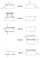
- figure 1 The general principle of such process is illustrated in figure 1 , which comprises figures 1a to 1e to show the successive main steps of such a known principle.
- Figure 1a shows a top wafer 10, and a handle wafer 20.
- the top wafer 10 has been implanted with one or more species in order to form an embrittlement zone 11.
- This top wafer 10 is covered by an insulator layer 12.
- the surface 100 of this insulator layer is to be contacted with a surface 200 of the handle wafer, for a direct bonding.
- Figure 1b shows the activation of the front surfaces 100 and 200 by a plasma, in a plasma chamber.
- this activation creates an activated region 101 on the front surface 100 of the top wafer 10, and an activated region 201 on the front surface 200 of the handle wafer 20.
- This activation also generates contaminants due to the exposure of the wafers to a plasma.
- Such contaminants are more particularly illustrated by references 111 and 211 on the respective back faces 110, 210 of the wafers, as the front faces receive significantly less contaminants than the back faces (as an example, the plasma activation of a silicon wafer typically generates a contaminant concentration of about 2.10 10 atoms/cm 2 on the "front" surface which is to be activated and which faces the inner space of the plasma chamber, the contaminant concentration being above 10 11 atoms/cm 2 on the back surface of the wafer).
- the wafer is disposed on a chuck in the plasma chamber.
- the chuck is adapted to perform the following functions:
- This set of functions that have to be performed by the chuck leads to selecting for making the chuck materials containing elements that are likely to contaminate the surface of the wafer in contact with said chuck (i.e. the back surface of the wafer, since it is the front surface which is directly exposed to the plasma).
- This material can typically be Al 2 O 3 based sintered ceramics.
- Figure 1d illustrates the direct bonding of top wafer 10 and handle wafer 20, these two wafers being bonded by their front surfaces. This bonding generates a multilayer 30 wafer (referred to as an "intermediate" multilayer wafer) which comprises in particular the embrittlement zone 11.
- Figure 1e hen illustrates the multilayer wafer 35 obtained after a detachment carried out at the embrittlement zone.
- This wafer 35 can be of the type SOI (Silicon On Insulator), SGOI (SiliconGermanium On Insulator), sSOI (strained Silicon On Insulator), GeOI (Germanium On Insulator), SiCOI (Silicon Carbide On insulator), SOQ (Silicon On Quartz), or any other type.
- SOI Silicon On Insulator
- SGOI Silicon Germanium On Insulator
- sSOI strained Silicon On Insulator
- GeOI Germanium On Insulator
- SiCOI Silicon Carbide On insulator
- SOQ Silicon On Quartz
- Figure 1e also illustrates the remaining part of the top wafer (part 15), which has been detached. This part can be treated and reused for a new process, e.g. for constituting a new top or a new handle wafer.
- This type of process illustrates that plasma activation could be advantageous for making multilayer wafers through a DBTP.
- plasma activation is in itself associated with another drawback, related to the contaminants generated by the activation.
- plasma activation generates a contamination of the wafer which is exposed to the plasma, in particular on the back surface of the wafer.
- This "contamination” corresponds to a deposit of metallic elements (e.g. Al, Fe, Ni, Zn, Cr, Ti, Ca, Mg, Y, altogether that may be incorporated in fine particles, on the surface of the wafer, or absorbed in said surface in the case of isolated atoms, molecules or ions.
- metallic elements e.g. Al, Fe, Ni, Zn, Cr, Ti, Ca, Mg, Y, .
- Such deposit of metallic elements can be observed with levels of contamination in the order of 5.10 11 - 5.10 12 atoms/cm 2 on at least some areas of the surface of the exposed wafer.
- Such concentrations are too high for a multilayer wafer which is to be subject to further thermal treatments (e.g. a high temperature annealing at temperatures above 1000°C for smoothing the surface of the wafer, or further treatments carried out on the multilayer wafer for integrating components into the wafer).
- further thermal treatments e.g. a high temperature annealing at temperatures above 1000°C for smoothing the surface of the wafer, or further treatments carried out on the multilayer wafer for integrating components into the wafer).
- the invention proposes a method for transferring from a top donor wafer a layer of material onto a receiving handle wafer, the top and receiving wafers comprising respective surfaces to be bonded, the method comprising:
- Figure 2 (which comprises figures 2a-2e ) shows the main steps of a first embodiment of the invention.
- Figure 2a thus shows a top wafer 10 with an implanted embrittlement zone 11, and a handle wafer 20.
- the front surfaces 100 and 200 of top wafer 10 and handle wafer 20 can undergo preliminary treatments for preparing the surfaces to be bonded.
- These preliminary treatments can include a Chemical-Mechanical Polishing (CMP) and/or one or more cleanings with a cleaning solution (such as RCA, SPM+RCA, ).
- CMP Chemical-Mechanical Polishing
- a cleaning solution such as RCA, SPM+RCA, .
- the top wafer 10 can be made of Si, SiGe, Ge, SiC, or in any other semiconductor material.
- the handle wafer 20 can be made of Si, fused silica, SiC, glass (all these materials being possibly in crystalline, polycrystalline or amorphous form), or in any other semiconductor material.
- the embrittlement zone 11 can have been made by introduction of species in the top wafer (this "introduction being carried out e.g. as an implantation and/or by diffusion, or by any other known technique).
- the "introduction" of species is an implantation of species
- such implantation can be an implantation of only one species (such as e.g. H or He). It can also have been made by implantation of several species (i.e. co-implantation), for example H and He.
- the front surface 100 of the top wafer is the surface of an oxide layer (e.g. a deposit of SiO2, or an oxidized region of the underlying material).
- an oxide layer e.g. a deposit of SiO2, or an oxidized region of the underlying material.
- Figure 2b illustrates an activation step, during which the front surface 100 of the top is exposed to a plasma.
- This activation step like all activation steps mentioned in the different embodiments described in this text - more generally corresponds to a treatment step of a surface to be bonded, with a generation of a contamination on the surface of the wafer which is opposite to the surface treated.
- the back surface 110 of top 10 is therefore covered by a region 111 which is contaminated with metallic contaminants such as those mentioned above (see figure 2c ).
- this contamination on the back surface of the top wafer corresponds to contaminant concentrations which is typically higher than the maximum concentration generally tolerated.
- the handle wafer 20 is not exposed to any plasma. Therefore, no contamination is deposited on the surfaces of said handle wafer.
- the following step is the direct bonding of the top wafer and the handle wafer, for making an intermediate multilayer wafer 30 ( Figure 2d ).
- this removal is carried out by detaching the excess material as delimited in the top by the embrittlement zone 11.
- the remainder 15 of the top is detached from the intermediate wafer 30.
- the removal can also be carried out according to any method known for BTPs.
- This removal can therefore be carried out by etching the back face of the top wafer 10 (i.e. the face of the top wafer which is opposed to the front surface 100), on the intermediate wafer 30.
- the removal step can also be performed in accordance with the ELTRAN ® method.
- embrittlement zone has previously been made by porous material, and here again no implantation is necessary.
- the multilayer wafer 35 obtained does not comprise a heavy contamination generated on a back surface of a wafer whose front surfaces would have been exposed to a plasma for its activation.
- this multilayer wafer shall then undergo additional thermal treatments, some of these thermal treatments being as mentioned before carried out at high temperatures (e.g. smoothing annealing at temperatures above 1000°C).
- this first embodiment of the invention allows to make a multilayer wafer with a DBTP, without having said multilayer wafer polluted by a heavy concentration of contaminants.
- the contaminant concentrations which can be observed on the front face of the exposed top after the activation step are in the order of 2.10 10 atoms/cm2, which is a generally acceptable concentration level.
- the removal step illustrated in figure 2e is carried out by detaching the top wafer at the implanted embrittlement zone 11.
- This detachment can result from a mechanical and/or thermal action.
- the temperature should be kept at moderated values, in order to avoid any diffusion of contaminants which would have been generated on the front surfaces 100, 200 (and would therefore be located in the vicinity of the bonding interface).
- Typical values of moderated temperatures for such splitting annealing are 300-500°C, for a multilayer wafer such as an SOI.
- the implantation of the top for creating the embrittlement zone 11 can advantageously be made with more than one species (co-implantation, e.g. of H+He).
- co-implantation allows a reduction of the temperature for the splitting annealing ; the splitting at an embrittlement zone created by co-implantation (e.g; H+He into a Si top wafer) occurs (for a given global implantation dose - i.e. the sum of the doses of all implanted species-which can typically be a "standard" implantation dose of e.g. 5.10 16 atoms/cm 2 - and more generally a few 10 16 atoms/cm 2 ) at lower temperatures than it would have occurred in the same top wafer implanted with the same global implantation dose, but with only one species.
- a standard implantation dose of e.g. 5.10 16 atoms/cm 2 - and more generally a few 10 16 atoms/cm 2
- a co-implantation (e.g. with H+He) therefore constitutes a favourable feature for performing a splitting annealing at moderated temperatures as mentioned above. And such co-implantation even allows a further reduction of the temperature for the splitting annealing.
- this temperature can remain under 350°C - it can in particular be in a range as low as 200-300°C.
- Figure 3 (which comprises figures 3a-3f ) shows the main steps of a second embodiment of the invention.
- Figure 3a illustrates - as figures 1a and 2a - a top wafer 10 and a handle wafer 20.
- the materials of the top and the handle wafers can be the identical to the materials mentioned in reference to the first embodiment described above.
- the top wafer has been implanted with one or more species for generating an embrittlement zone 11.
- implanted embrittlement zone is only a particular illustration corresponding to the case where the invention is embodied with a Smart Cut TM -type method, whereas any type of DBTP can be used.
- Figure 3b illustrates the step of activation through exposure to a plasma.
- the front surface of the top wafer 10 and/or of the handle wafer 20 can be exposed.
- the first embodiment described above can be combined with the second embodiment.
- Figures 3b-3d illustrate the particular case where both top and handle wafers are activated by a plasma.
- Figure 3c thus illustrates highly contaminated regions 111 and 211 respectively associated to the back surfaces of the top and the handle wafers.
- Figure 3d illustrates the direct bonding of the top and handle wafers, with their front surfaces contacted.
- the bonding is followed (preferably immediately followed) by a cleaning step ( figure 3e ) for removing the contaminants from the highly contaminated regions 111 and 211 on the intermediate multilayer wafer 30 (or from the region 111 or 211 which has been formed, if only one such highly contaminated region has been formed because only one wafer was activated by a plasma before bonding).
- the region 111 is said to be associated to a first "main" surface of the intermediate multilayer wafer 30, and the region 211 is said to be associated to a second "main” surface of the intermediate multilayer wafer 30.
- This cleaning step is carried out on the intermediate multilayer wafer 30 which has been made by the direct bonding of the top and handle wafers, with a cleaning solution able to eliminate contaminants.
- a SC2 solution or a HF solution can be used for that purpose.
- the cleaning step is carried out before the wafer undergoes any high temperature treatment (i.e. any thermal treatment above 900°C).
- the "cleaning step" illustrated in figure 3e can be composed of several successive cleanings.
- Such cleaning is carried out on the intermediate multilayer wafer 30. This differs from the cleaning operations known in the art since these cleaning are usually carried out on single-layer wafers such as bulk silicon wafers.
- Each cleaning of the cleaning step can be carried out as a wet cleaning, i.e. by immersing the wafer to be cleaned in a bath made of the cleaning solution.
- this second embodiment which has the cleaning performed after the bonding, further allows to use a solution such as a SC2 or HF solution, which is known to efficiently remove metallic contaminants.
- a SC2 or HF solution would indeed have been associated to problems if used for cleaning the top and/or handle wafer before their bonding together : in such case, the SC2 or HF solution would have removed the undesirable contaminants, but would also have deactivated the surfaces to be bonded - thus losing the benefit of the plasma activation.
- Figure 3f illustrates the removal step of the excess material of the top.
- An advantage of this second embodiment is that in the case of a removal carried out in a way which generates a remainder (as illustrated in the left part of figure 3f ), such remainder has already been cleaned by the cleaning step.
- the invention ensures that no wafer surfaces can undergo high temperature thermal treatments if said surface is heavily contaminated.
Abstract
• a treatment step for treating at least a surface to be bonded, the treatment of a given surface of a wafer generating on the opposed surface of said wafer a contamination,
• a bonding step for direct bonding the surfaces to be bonded of the top and handle wafers, in order to form an intermediate multilayer wafer (30),
• a removal step for removing excess material from the top wafer,
the method being characterized in that during the treatment step only the surface to be bonded of the top wafer is treated.


Description
- The invention generally concerns the manufacturing of multilayer wafer including materials selected from semiconductor materials, and used in applications in microelectronics, optics, optoelectronics and/or optronics.
- More precisely, the invention concerns the processes for transferring from a "top" wafer (or donor wafer - these terms being herein understood as equivalent) a layer of a semiconductor material onto a "handle" (or receiving wafer, or "base" wafer - these terms being herein understood as equivalent), in order to make a multilayer wafer.
- Several main types of such processes are known.
- Many of these processes imply a bonding step for bonding the handle and the top wafers, before a removal of the excess material from the bonded top wafer.
- We will refer to such processes which imply a bonding step as "bond and transfer processes", or "BTP" processes.
- It is specified that the definitions and corresponding acronyms given in this document are provided for the purpose of clearly defining the invention which is the subject matter to be protected by this document.
- These definitions/acronyms are therefore intended to be used only for the purpose of understanding this particular subject matter. They are not intended to be used for any other purpose, e.g. for the interpretation of other documents such as other patents or patent applications in the name of the Applicant (unless otherwise specified).
- The known types of BTP processes include:
- the BESOI-type process (the removal of material from the top wafer is performed through an etching of said top wafer),
- the ELTRAN™-type process (the removal is performed through a detachment of the excess material said detachment resulting from the attack of a porous region of the top wafer),
- the Smart Cut™-type process (the removal is performed through a detachment of the excess material said detachment resulting from the splitting of the top wafer at an embrittlement region obtained by implantation of the top wafer with at least one species. It is specified that a general description of the main steps of a non limiting embodiment of this type of method can be found in SILICON-ON-INSULATOR TECHNOLOGY: Material to VLSI, 2nd Edition (Jean-Pierre COLINGE).
- The bonding step of such processes is generally performed without adding between the top and handle wafers any adhesive (such as a resin).
- We will refer to such bonding without adhesive as "direct bonding". And a BTP comprising such a direct bonding will be referred to as "Direct bonding and transfer process" (DBTP).
- For such direct bonding, the surfaces to be bonded must be very smooth (i-e. present a very low roughness).
- And it is possible to provide a smooth surface over a first wafer which is to be bonded with a second wafer through a direct bonding, e.g. by building a "bonding layer" (e.g. with an oxide layer) over said first wafer, and/or by submitting the surface of the first wafer to a specific treatment (e.g. polishing, ...).
- A bonding of the surfaces of two wafers generates between the bonded surfaces a bonding interface associated with a given bonding energy (the higher this energy the stronger the bond).
- The bonding energy obtained by direct bonding two wafers without any additional treatment is sometimes not high enough.
- This is the case in particular when it is desired to obtain with the bonding of two or more wafers a multilayer wafer (each initial wafer bringing a layer" to the multilayer wafer thus obtained), with a high energy bond (i.e. a bonding energy typically greater than 500mJ/m2) between the bonded wafers. In such cases, the bonded wafers are thus subjected to a "bonding heat treatment" (BHT) which improves the strength of the bonding.
- More precisely, such BHT is generally carried out at high temperatures (i.e. at temperatures of 900°C or higher). We will refer to such a high temperature BHT carried out at temperature higher than 900°C as a "HT BHT".
- Such HT BHT reinforces the bonding interface and can bring its bonding energy up to a desired level. As an illustration, the bonding energy between a Si wafer and a Si or SiO2 wafer is maximized after a HT BHT at temperatures in the order of 1100-1200°C.
- The bonding energy obtained after a HT BHT can e.g. be 2 to 2.5 J/m2 for a bonding of Si/Si, SiO2/SiO2, or Si/SiO2.
- Such HT BHT can therefore allow the manufacturing of multilayer wafers with adequate bonding energy between the bonded layers of the wafer.
- However, it can be undesirable to carry out a HT BHT on a multilayer wafer.
- This is the case e.g. when the layers of the multilayer wafer have respective coefficients of thermal expansion (CTE) which are significantly different.
- In such case indeed, the layers associated to different CTEs will undergo expansions of different magnitudes when exposed to a HT BHT. This can lead to negative effects such as a warp of the wafers, or even the generation of defects such as dislocations in the crystalline structure of the wafers.
- It can also be undesirable to carry out a HT BHT on a bonded multilayer wafer for other reasons, e.g. the wafer already comprises components totally or partially elaborated (such wafer is usually called "structured substrate"), or the material of the wafer is likely to be altered by a high temperature treatment (e.g. case of a wafer comprising sharp doping profile like boron, phosphorous or comprising metastable layers that would be altered by HT BUT, like low k materials, high k materials or comprising layers with metallic elements like Al2O3 or TiN),
- In order to avoid such drawbacks and nevertheless obtain a high bonding energy between bonded layers of a multilayer wafer, techniques of high bonding energy at low temperatures have been developed.
- In one of these techniques the surfaces to be bonded are "activated" by their exposure to a plasma, before being contacted together.
- Such technique will be referred to as "plasma activation" technique.
- Plasma activation is advantageous since it allows obtaining high bonding energy with a BHT which is carried out after contacting the surfaces to be bonded, but which remains limited to a low temperature BHT ("LT BHT").
- And plasma activation has been proposed for DBTPs as a solution for obtaining a high energy bonding without requiring carrying out a HT BHT on a bonded multilayer wafer.
- A general illustration of such known DBTP is given in "Ultra-thin strained-silicon-on-insulator and SiGe-on-insulator created using low-temperature wafer bonding and metastable layers", Taraschi et al., J. Electrochem. Soc. Vol. 151, N° 1, p. 47 (2004).
- This article discloses a Smart Cut™-type process in which prior to the wafer bonding step (between a top and a handle wafers) a plasma activation can be carried out on the surfaces to be bonded.
- The general principle of such process is illustrated in
figure 1 , which comprisesfigures 1a to 1e to show the successive main steps of such a known principle. -
Figure 1a shows atop wafer 10, and a handle wafer 20. - The
top wafer 10 has been implanted with one or more species in order to form anembrittlement zone 11. - This
top wafer 10 is covered by aninsulator layer 12. - The
surface 100 of this insulator layer is to be contacted with asurface 200 of the handle wafer, for a direct bonding. - These two
surfaces wafers - And the opposite surfaces of these two wafers (respectively
surface 110 and surface 210) are referred to as the respective "back" surfaces of these wafers. -
Figure 1b shows the activation of thefront surfaces - As illustrated in
figure 1c , this activation creates an activatedregion 101 on thefront surface 100 of thetop wafer 10, and an activatedregion 201 on thefront surface 200 of the handle wafer 20. - This activation also generates contaminants due to the exposure of the wafers to a plasma.
- Such contaminants are more particularly illustrated by
references respective back faces - This is due in particular to the fact that the physical contacts between each wafer and supporting elements (e.g. chucks) associated to the plasma chamber are made on the back surface of the wafer.
- In commercially available equipment for microelectronic application, the wafer is disposed on a chuck in the plasma chamber.
The chuck is adapted to perform the following functions: - receive and hold the wafer very tightly in place during exposure to the plasma.
- regulate the wafer temperature during plasma exposure, by temperature diffusion,
- act as a an electrode to transfer polarisation (bias voltage) to the wafer.
- This set of functions that have to be performed by the chuck leads to selecting for making the chuck materials containing elements that are likely to contaminate the surface of the wafer in contact with said chuck (i.e. the back surface of the wafer, since it is the front surface which is directly exposed to the plasma). This material can typically be Al2O3 based sintered ceramics.
-
Figure 1d illustrates the direct bonding oftop wafer 10 and handlewafer 20, these two wafers being bonded by their front surfaces. This bonding generates amultilayer 30 wafer (referred to as an "intermediate" multilayer wafer) which comprises in particular theembrittlement zone 11. -
Figure 1e hen illustrates themultilayer wafer 35 obtained after a detachment carried out at the embrittlement zone. Thiswafer 35 can be of the type SOI (Silicon On Insulator), SGOI (SiliconGermanium On Insulator), sSOI (strained Silicon On Insulator), GeOI (Germanium On Insulator), SiCOI (Silicon Carbide On insulator), SOQ (Silicon On Quartz), or any other type. -
Figure 1e also illustrates the remaining part of the top wafer (part 15), which has been detached. This part can be treated and reused for a new process, e.g. for constituting a new top or a new handle wafer. - This type of process illustrates that plasma activation could be advantageous for making multilayer wafers through a DBTP.
- However, plasma activation is in itself associated with another drawback, related to the contaminants generated by the activation.
- Indeed, as mentioned above plasma activation generates a contamination of the wafer which is exposed to the plasma, in particular on the back surface of the wafer.
- This "contamination" corresponds to a deposit of metallic elements (e.g. Al, Fe, Ni, Zn, Cr, Ti, Ca, Mg, Y, ...) that may be incorporated in fine particles, on the surface of the wafer, or absorbed in said surface in the case of isolated atoms, molecules or ions.
- Such deposit of metallic elements can be observed with levels of contamination in the order of 5.1011 - 5.1012 atoms/cm2 on at least some areas of the surface of the exposed wafer.
- Such concentrations are too high for a multilayer wafer which is to be subject to further thermal treatments (e.g. a high temperature annealing at temperatures above 1000°C for smoothing the surface of the wafer, or further treatments carried out on the multilayer wafer for integrating components into the wafer).
- Indeed, the contaminants of a multilayer wafer which would be exposed to such high temperatures treatments would undergo a diffusion in the volume of the wafer, and significantly alter the properties (in particular the electrical properties) of the wafer and of its components.
- And contaminant concentrations such as mentioned above and resulting from a plasma activation are thus significantly higher than the specifications of maximum contamination level generally in use in the industry of manufacturing the multilayer wafers and their associated components (these specifications being in the order of 5.1010 atoms/cm2, or even less).
- Thus, carrying out a direct bonding transfer process (such as e.g. a Smart Cut™ process) with an activation of the surfaces to be bonded as in the known state of the art, in order to make multilayer wafers, is associated to some drawbacks.
- And it is specified that if these drawbacks have been exposed hereabove in reference to a plasma activation, similar drawbacks can also be associated to the activation of a surface which is different from a plasma activation (e.g. an oxidation and/or a chemical activation...).
- It is an object of the invention to overcome the above mentioned drawbacks.
- For this purpose the invention proposes a method for transferring from a top donor wafer a layer of material onto a receiving handle wafer, the top and receiving wafers comprising respective surfaces to be bonded, the method comprising:
- a treatment step for treating at least a surface to be bonded, the treatment of a given surface of a wafer generating on the opposed surface of said wafer a contamination,
- a bonding step for direct bonding the surfaces to be bonded of the top and handle wafers, in order to form an intermediate multilayer wafer,
- a removal step for removing excess material from the top wafer,
- Preferred but non-limiting aspects of such a method are the following:
- said treatment step is a surface activation step,
- said contamination of the wafer surface which is opposed to the activated surface corresponds to a metallic contaminants concentration above 1011 atoms/cm2,
- said treatment is carried out through the exposure of the surface(s) to be treated to a plasma,
- said removal step is carried out by detaching said excess material from the top wafer,
- said detachment is carried out at an embrittlement zone which has been made by introduction of at least one species in the top wafer,
- said introduction of species is carried out through an implantation of species,
- said implantation is a co-implantation of at least two species,
- said implantation is carried out with a global implantation dose of a few 1016 atoms/cm2,
- said removal step is carried out through a splitting annealing carried out at temperatures remaining under 350°C,
- said temperature for the splitting annealing is in a range between 200°C and 300°C,
- the method comprises :
- A treatment step for treating at least a surface to be bonded, the treatment of a given surface of a wafer generating on the opposed surface of said wafer a contamination,
- a bonding step for direct bonding the surfaces to be bonded of the top and handle wafers, in order to form an intermediate multilayer wafer,
- a removal step for removing excess material from the top wafer,
the method being characterized in that it comprises between the bonding step and the removal step a cleaning step for removing from the exposed main surfaces of the intermediate multilayer wafer contaminants brought by the treatment step,
- said treatment step is a surface activation step,
- said contamination of the wafer surface which is opposed to the activated surface corresponds to a contaminants concentration above 1011 atoms/cm2,
- said treatment is carried out through the exposure of the surface(s) to be treated to a plasma,
- during the treatment step only a surface of the top wafer is treated,
- said cleaning step is carried out immediately after said bonding step,
- said cleaning step is carried out before any high temperature thermal treatment,
- said cleaning step is a wet cleaning,
- said cleaning step is carried out with a SC2 solution and/or a HF solution,
- said cleaning step is carried out with a mono face cleaning equipment,
- the top wafer is made of Si, or SiGe, SiC, or Ge,
- the handle wafer is made of Si, fused silica, SiC, or glass,
- the method further comprises a high temperature thermal treatment of the structure which comprises the handle wafer and the part of the top wafer which has not been removed,
- said high temperature thermal treatment is carried out at a temperature greater than 900°C.
- Other aspects and advantages of the invention shall appear when reading the following description made in reference to the accompanying drawings, on which (in addition to
figure 1 which has already be commented in reference to a principal known in the state of the art): -
figure 2 is a diagrammatical flowchart of a process according to a first embodiment of the invention, -
figure 3 is a diagrammatical flowchart of a process according to a second embodiment of the invention. - It is specified that the two embodiments which shall be presented hereunder can be combined.
- It is also specified that on the figures which shall be commented hereunder, the elements and features which are identical or similar to those commented with reference to
figure 1 shall be associated to the same reference numeral. -
Figure 2 (which comprisesfigures 2a-2e ) shows the main steps of a first embodiment of the invention. - These steps reproduce some of the steps 1a-1e commented above.
-
Figure 2a thus shows atop wafer 10 with an implantedembrittlement zone 11, and ahandle wafer 20. - At this stage the
front surfaces top wafer 10 and handlewafer 20 can undergo preliminary treatments for preparing the surfaces to be bonded. These preliminary treatments can include a Chemical-Mechanical Polishing (CMP) and/or one or more cleanings with a cleaning solution (such as RCA, SPM+RCA, ...). - The
top wafer 10 can be made of Si, SiGe, Ge, SiC, or in any other semiconductor material. - The
handle wafer 20 can be made of Si, fused silica, SiC, glass (all these materials being possibly in crystalline, polycrystalline or amorphous form), or in any other semiconductor material. - The
embrittlement zone 11 can have been made by introduction of species in the top wafer (this "introduction being carried out e.g. as an implantation and/or by diffusion, or by any other known technique). - In the case where the "introduction" of species is an implantation of species, such implantation can be an implantation of only one species (such as e.g. H or He). It can also have been made by implantation of several species (i.e. co-implantation), for example H and He.
- Here again, the
front surface 100 of the top wafer is the surface of an oxide layer (e.g. a deposit of SiO2, or an oxidized region of the underlying material). -
Figure 2b illustrates an activation step, during which thefront surface 100 of the top is exposed to a plasma. - This activation step - like all activation steps mentioned in the different embodiments described in this text - more generally corresponds to a treatment step of a surface to be bonded, with a generation of a contamination on the surface of the wafer which is opposite to the surface treated.
- The
back surface 110 of top 10 is therefore covered by aregion 111 which is contaminated with metallic contaminants such as those mentioned above (seefigure 2c ). - And as mentioned above, this contamination on the back surface of the top wafer corresponds to contaminant concentrations which is typically higher than the maximum concentration generally tolerated.
- It shall be noted that during this activation step, only the top wafer is exposed to a plasma in order to be activated.
- The
handle wafer 20 is not exposed to any plasma. Therefore, no contamination is deposited on the surfaces of said handle wafer. - This selective exposure of the donor top wafer only is specific to this first embodiment of the invention.
- In the known experiments for using a plasma activation in a DBTP, both front surfaces of the top and of the handle wafers were exposed for activation by a plasma. In such experiments, the drawbacks associated to the contamination of a multilayer structure which could undergo further high temperature treatments had not been pointed out.
- It is to be noted that a reports on one of such experiments (see "Ultra-thin strained-silicon-on-insulator and SiGe-on-insulator created using low-temperature wafer bonding and metastable layers", Taraschi et al., J. Electrochem. Soc. Vol. 151, N° 1, p. 47 (2004)) mentions the plasma activation of only one of the wafers to be bonded.
- But this mention makes reference to the activation of the handle wafer, and not of the top wafer. And not surprisingly, there is no mention in this article of any problem associated to the contamination resulting from the plasma activation.
- The following step is the direct bonding of the top wafer and the handle wafer, for making an intermediate multilayer wafer 30 (
Figure 2d ). - The excess material from the top is then removed.
- In the illustration of this first embodiment presented on
figures 2a-2e , this removal is carried out by detaching the excess material as delimited in the top by theembrittlement zone 11. - In this particular case which refers to a Smart Cut™-type method, the
remainder 15 of the top is detached from theintermediate wafer 30. - The removal can also be carried out according to any method known for BTPs.
- This removal can therefore be carried out by etching the back face of the top wafer 10 (i.e. the face of the top wafer which is opposed to the front surface 100), on the
intermediate wafer 30. - In such case (which corresponds to a BESOI-type method), it is not necessary that any implantation has been carried out on the top wafer.
- The removal step can also be performed in accordance with the ELTRAN® method.
- In such case, the embrittlement zone has previously been made by porous material, and here again no implantation is necessary.
- In the case of a Smart Cut™-type or ELTRAN™-type method, a
remainder 15 shall be obtained. - In every cases (i.e. whatever the method used for removing the excess material of the top), the
multilayer wafer 35 obtained does not comprise a heavy contamination generated on a back surface of a wafer whose front surfaces would have been exposed to a plasma for its activation. - Indeed, in all cases the
heavy contamination region 111 which is on the back surface of the top wafer has been removed from themultilayer wafer 35. - This is particularly advantageous since this multilayer wafer shall then undergo additional thermal treatments, some of these thermal treatments being as mentioned before carried out at high temperatures (e.g. smoothing annealing at temperatures above 1000°C).
- And exposing a wafer comprising heavy concentrations of contaminants (e.g. concentrations above 1011 atoms/cm2) would generate an unacceptable and irreversible diffusion of the contaminants into the wafer.
- In the case of a method generating a
remainder 15, the only heavy contamination (region 111) is on said remainder, themultilayer wafer 35 being totally free of such heavy contamination. - Therefore, this first embodiment of the invention allows to make a multilayer wafer with a DBTP, without having said multilayer wafer polluted by a heavy concentration of contaminants.
- It is specified that the contaminant concentrations which can be observed on the front face of the exposed top after the activation step are in the order of 2.1010 atoms/cm2, which is a generally acceptable concentration level.
- The removal step illustrated in
figure 2e is carried out by detaching the top wafer at the implantedembrittlement zone 11. - This detachment can result from a mechanical and/or thermal action.
- In the case of a thermal action (i.e. a splitting annealing), the temperature should be kept at moderated values, in order to avoid any diffusion of contaminants which would have been generated on the
front surfaces 100, 200 (and would therefore be located in the vicinity of the bonding interface). - Typical values of moderated temperatures for such splitting annealing are 300-500°C, for a multilayer wafer such as an SOI.
- And always in the specific case of the use of a Smart Cut™-type method as illustrated in
figures 1a-1e , the implantation of the top for creating theembrittlement zone 11 can advantageously be made with more than one species (co-implantation, e.g. of H+He). - Indeed, such co-implantation allows a reduction of the temperature for the splitting annealing ; the splitting at an embrittlement zone created by co-implantation (e.g; H+He into a Si top wafer) occurs (for a given global implantation dose - i.e. the sum of the doses of all implanted species-which can typically be a "standard" implantation dose of e.g. 5.1016 atoms/cm2 - and more generally a few 1016 atoms/cm2) at lower temperatures than it would have occurred in the same top wafer implanted with the same global implantation dose, but with only one species.
- For more details on the conditions of such a co-implantation which allows a reduction of the temperature for the splitting annealing, with a "standard" global dose, reference is made to
WO/042779 - A co-implantation (e.g. with H+He) therefore constitutes a favourable feature for performing a splitting annealing at moderated temperatures as mentioned above. And such co-implantation even allows a further reduction of the temperature for the splitting annealing.
- For a H+He co-implantation in a Si top with a global implantation dose of a few 1016 atoms/cm2, this temperature can remain under 350°C - it can in particular be in a range as low as 200-300°C.
-
Figure 3 (which comprisesfigures 3a-3f ) shows the main steps of a second embodiment of the invention. -
Figure 3a illustrates - asfigures 1a and 2a - atop wafer 10 and ahandle wafer 20. - The materials of the top and the handle wafers can be the identical to the materials mentioned in reference to the first embodiment described above.
- Here again, the top wafer has been implanted with one or more species for generating an
embrittlement zone 11. - But here again, such implanted embrittlement zone is only a particular illustration corresponding to the case where the invention is embodied with a Smart Cut™-type method, whereas any type of DBTP can be used.
- And more generally, unless otherwise specified, all information given above for the first embodiment is applicable to this second embodiment.
-
Figure 3b illustrates the step of activation through exposure to a plasma. - During this step, the front surface of the
top wafer 10 and/or of thehandle wafer 20 can be exposed. - If only the
top wafer 10 is exposed to a plasma for activation, the first embodiment described above can be combined with the second embodiment. -
Figures 3b-3d illustrate the particular case where both top and handle wafers are activated by a plasma. -
Figure 3c thus illustrates highly contaminatedregions - Of course, if only the top wafer is activated there would be only a
region 111 and if only the handle wafer is activated there would be only aregion 211. -
Figure 3d illustrates the direct bonding of the top and handle wafers, with their front surfaces contacted. - In this second embodiment, the bonding is followed (preferably immediately followed) by a cleaning step (
figure 3e ) for removing the contaminants from the highly contaminatedregions region - The
region 111 is said to be associated to a first "main" surface of theintermediate multilayer wafer 30, and theregion 211 is said to be associated to a second "main" surface of theintermediate multilayer wafer 30. - This cleaning step is carried out on the
intermediate multilayer wafer 30 which has been made by the direct bonding of the top and handle wafers, with a cleaning solution able to eliminate contaminants. A SC2 solution or a HF solution can be used for that purpose. - The cleaning step is carried out before the wafer undergoes any high temperature treatment (i.e. any thermal treatment above 900°C).
- The "cleaning step" illustrated in
figure 3e can be composed of several successive cleanings. - Such cleaning is carried out on the
intermediate multilayer wafer 30. This differs from the cleaning operations known in the art since these cleaning are usually carried out on single-layer wafers such as bulk silicon wafers. - Each cleaning of the cleaning step can be carried out as a wet cleaning, i.e. by immersing the wafer to be cleaned in a bath made of the cleaning solution.
- It is however also possible to perform such cleaning with a monoface cleaning equipment, which projects a controlled spray or jet of cleaning solution selectively, only on the surface to be cleaned.
- Concerning the cleaning step it is to be noted that the applicant has observed that contrary to what one might have expected, the use of a cleaning solution on a
multilayer wafer 30 whose layers have already been bonded together produces very satisfactory results. - Indeed, the prior art tends to indicate that such cleaning should be avoided because the cleaning solution might be infiltrated at the bonding interface (see e.g. "Semiconductor on Wafer Bonding: Science and Technology" - Tong and Gösele, sponsored by the Electrochemical Society, Inc., a Wiley-Interscience Publication, 1999). Such infiltrations would be associated to risks of degrading the quality of the bonding, or even undo the bond between the bonded wafers.
- In addition, when considering the prior art one would consider that the manipulations associated to a cleaning step would favour debonding of the bonded wafers.
- Moreover, one would also consider that the cleaning step would most probably lower the bonding energy at the edge of the bonding interface of the bonded wafer.
- Therefore, a cleaning step carried out as in this second embodiment goes against the teachings of the prior art.
- And the specific process provided by this second embodiment, which has the cleaning performed after the bonding, further allows to use a solution such as a SC2 or HF solution, which is known to efficiently remove metallic contaminants.
- A SC2 or HF solution would indeed have been associated to problems if used for cleaning the top and/or handle wafer before their bonding together : in such case, the SC2 or HF solution would have removed the undesirable contaminants, but would also have deactivated the surfaces to be bonded - thus losing the benefit of the plasma activation.
- It therefore appears that the specific method proposed in this second embodiment also corresponds to an advantageous process which allows the manufacturing of a multilayer wafer through a DBTP, with a LT BHT.
-
Figure 3f illustrates the removal step of the excess material of the top. Here again, all comments made above about the first embodiment are applicable. - An advantage of this second embodiment is that in the case of a removal carried out in a way which generates a remainder (as illustrated in the left part of
figure 3f ), such remainder has already been cleaned by the cleaning step. - It is specified that if the description given above of embodiments of the invention is focused on the case of an activation (or several activations) carried out through the exposure to a plasma ("plasma activation"), such activation can alternatively be carried out under different forms (e.g. oxidation and/or chemical activation ...).
- In all cases the activation is:
- intended to enhance the bonding energy associated to a bonding of the surface which is activated (said surface can generally be be referred to as a "front" surface),
- associated to the generation of a heavy contamination on the "back" surface which is opposed to the "front" surface to be activated (with a "heavy" contamination being understood as corresponding to a contaminant concentration above 1011 atoms/cm2).
- And in all embodiments the invention ensures that no wafer surfaces can undergo high temperature thermal treatments if said surface is heavily contaminated.
Claims (13)
- Method for transferring from a top donor wafer (10) a layer of material onto a receiving handle wafer (20), the top and receiving wafers comprising respective surfaces to be bonded, the method comprising:- a treatment step for treating at least a surface to be bonded, the treatment of a given surface of a wafer generating on the opposed surface of said wafer a contamination,- a bonding step for direct bonding the surfaces to be bonded of the top and handle wafers, in order to form an intermediate multilayer wafer (30),- a removal step for removing excess material from the top wafer,the method being characterized in that during the treatment step, only the surface to be bonded of the top wafer is treated and in that said removal step is carried out by detaching said excess material from the top wafer, at an implanted embrittlement zone (11), made by introduction of at least one species in the top wafer, said detachment being conducted by an annealing between 300°C and 500°C.
- Method according to claim 1, characterized in that said treatment step is a surface activation step.
- Method according to claims 1 or 2, characterized in that said contamination corresponds to a deposit of metallic elements.
- Method according to claim 3, characterized in that the contamination of the wafer surface which is opposed to the treated surface correspond to a metallic contaminants concentration above 1011 atoms/cm2.
- Method according to any one of claims 2 to 4, characterized in that the contaminant concentration of the activated surface is in the order of 2.1010 atoms/cm2.
- Method according to any of the preceding claims, characterized in that said treatment is carried out through the exposure of the surface(s) to be treated to a plasma.
- Method according to any of the preceding claims, characterized in that said introduction of species is carried out through an implantation of species.
- Method according to any one of the claims 1 to 7, characterized in that said implantation is a co-implantation of at least two species.
- Method according to claim 8, characterized in that said implantation is carried out with a global implantation dose of a few 1016 atoms/cm2.
- Method according to claims 8 or 9, characterized in that said removal step is carried out through a splitting annealing carried out at temperatures remaining under 350°C.
- Method according to any of the preceding claims, characterized in that the top wafer is made of Si, or SiGe, SiC, or Ge.
- Method according to any of the preceding claims, characterized in that the handle wafer is made of Si, fused silica, SiCl or glass.
- Method according to any of the preceding claims, characterized in that the method further comprises a high temperature thermal treatment of the structure which comprises the handle wafer and the part of the top wafer which has not been removed, said high temperature thermal treatment being carried out at temperatures higher than 900°C.
Applications Claiming Priority (2)
| Application Number | Priority Date | Filing Date | Title |
|---|---|---|---|
| EP04769581A EP1792337B1 (en) | 2004-09-21 | 2004-09-21 | Transfer method with a treatment of a surface to be bonded |
| PCT/IB2004/003275 WO2006032946A1 (en) | 2004-09-21 | 2004-09-21 | Transfer method with a treatment of a surface to be bonded |
Related Parent Applications (2)
| Application Number | Title | Priority Date | Filing Date |
|---|---|---|---|
| EP04769581A Division EP1792337B1 (en) | 2004-09-21 | 2004-09-21 | Transfer method with a treatment of a surface to be bonded |
| EP04769581.2 Division | 2004-09-21 |
Publications (2)
| Publication Number | Publication Date |
|---|---|
| EP2048706A1 true EP2048706A1 (en) | 2009-04-15 |
| EP2048706B1 EP2048706B1 (en) | 2012-12-12 |
Family
ID=34959038
Family Applications (2)
| Application Number | Title | Priority Date | Filing Date |
|---|---|---|---|
| EP04769581A Active EP1792337B1 (en) | 2004-09-21 | 2004-09-21 | Transfer method with a treatment of a surface to be bonded |
| EP08166193A Active EP2048706B1 (en) | 2004-09-21 | 2004-09-21 | Transfer method with a treatment of a surface to be bonded |
Family Applications Before (1)
| Application Number | Title | Priority Date | Filing Date |
|---|---|---|---|
| EP04769581A Active EP1792337B1 (en) | 2004-09-21 | 2004-09-21 | Transfer method with a treatment of a surface to be bonded |
Country Status (8)
| Country | Link |
|---|---|
| US (2) | US7615464B2 (en) |
| EP (2) | EP1792337B1 (en) |
| JP (1) | JP5101287B2 (en) |
| KR (1) | KR20120011095A (en) |
| CN (1) | CN101027769B (en) |
| AT (1) | ATE469438T1 (en) |
| DE (1) | DE602004027422D1 (en) |
| WO (1) | WO2006032946A1 (en) |
Families Citing this family (13)
| Publication number | Priority date | Publication date | Assignee | Title |
|---|---|---|---|---|
| FR2865574B1 (en) * | 2004-01-26 | 2006-04-07 | Soitec Silicon On Insulator | METHOD FOR MANUFACTURING A DEMOUNTABLE SUBSTRATE |
| JP5064692B2 (en) * | 2006-02-09 | 2012-10-31 | 信越化学工業株式会社 | Manufacturing method of SOI substrate |
| US20070284730A1 (en) * | 2006-06-12 | 2007-12-13 | Wei Shi | Method, apparatus, and system for thin die thin thermal interface material in integrated circuit packages |
| FR2903808B1 (en) * | 2006-07-11 | 2008-11-28 | Soitec Silicon On Insulator | PROCESS FOR DIRECTLY BONDING TWO SUBSTRATES USED IN ELECTRONIC, OPTICAL OR OPTOELECTRONIC |
| US20080268617A1 (en) * | 2006-08-09 | 2008-10-30 | Applied Materials, Inc. | Methods for substrate surface cleaning suitable for fabricating silicon-on-insulator structures |
| CN101056339B (en) | 2006-11-06 | 2011-06-08 | 华为技术有限公司 | Method, system and device for mutual conversion between the ring back tone and ringing tone |
| US20100044827A1 (en) * | 2008-08-22 | 2010-02-25 | Kinik Company | Method for making a substrate structure comprising a film and substrate structure made by same method |
| US7927975B2 (en) | 2009-02-04 | 2011-04-19 | Micron Technology, Inc. | Semiconductor material manufacture |
| FR2962141A1 (en) * | 2010-06-30 | 2012-01-06 | Soitec Silicon On Insulator Technologies | METHOD FOR DEOXIDIZING A MULTILAYER STRUCTURE WITH FLUORHYDRIC ACID |
| US9252042B2 (en) * | 2011-01-25 | 2016-02-02 | Ev Group E. Thallner Gmbh | Method for permanent bonding of wafers |
| US9305865B2 (en) * | 2013-10-31 | 2016-04-05 | Micron Technology, Inc. | Devices, systems and methods for manufacturing through-substrate vias and front-side structures |
| FR2977069B1 (en) | 2011-06-23 | 2014-02-07 | Soitec Silicon On Insulator | METHOD FOR MANUFACTURING A SEMICONDUCTOR STRUCTURE USING TEMPORARY COLLAGE |
| FR3007892B1 (en) * | 2013-06-27 | 2015-07-31 | Commissariat Energie Atomique | METHOD FOR TRANSFERRING A THIN LAYER WITH THERMAL ENERGY SUPPLY TO A FRAGILIZED AREA VIA AN INDUCTIVE LAYER |
Citations (9)
| Publication number | Priority date | Publication date | Assignee | Title |
|---|---|---|---|---|
| EP1039513A2 (en) * | 1999-03-26 | 2000-09-27 | Canon Kabushiki Kaisha | Method of producing a SOI wafer |
| EP1050901A2 (en) * | 1999-04-30 | 2000-11-08 | Canon Kabushiki Kaisha | Method of separating composite member and process for producing thin film |
| US6368938B1 (en) * | 1999-10-05 | 2002-04-09 | Silicon Wafer Technologies, Inc. | Process for manufacturing a silicon-on-insulator substrate and semiconductor devices on said substrate |
| US20030227057A1 (en) * | 2002-06-07 | 2003-12-11 | Lochtefeld Anthony J. | Strained-semiconductor-on-insulator device structures |
| WO2004002779A1 (en) | 2002-07-01 | 2004-01-08 | Meridiana Investimenti Sagl | Emergency optical signalling device |
| EP1381086A1 (en) * | 2001-04-18 | 2004-01-14 | Shin-Etsu Handotai Co., Ltd | Production method for bonded substrates |
| WO2004008514A1 (en) * | 2002-07-12 | 2004-01-22 | Alexander Usenko | Process for forming a fragile layer inside of a single crystalline substrate |
| US20040097055A1 (en) * | 1997-07-18 | 2004-05-20 | Silicon Genesis Corporation | Gettering technique for wafers made using a controlled cleaving process |
| WO2004042779A2 (en) * | 2002-11-07 | 2004-05-21 | S.O.I.Tec Silicon On Insulator Technologies | Method of detaching a thin film at moderate temperature after co-implantation |
Family Cites Families (13)
| Publication number | Priority date | Publication date | Assignee | Title |
|---|---|---|---|---|
| US5395788A (en) * | 1991-03-15 | 1995-03-07 | Shin Etsu Handotai Co., Ltd. | Method of producing semiconductor substrate |
| JP3294934B2 (en) * | 1994-03-11 | 2002-06-24 | キヤノン株式会社 | Method for manufacturing semiconductor substrate and semiconductor substrate |
| US6150239A (en) * | 1997-05-31 | 2000-11-21 | Max Planck Society | Method for the transfer of thin layers monocrystalline material onto a desirable substrate |
| US5877070A (en) * | 1997-05-31 | 1999-03-02 | Max-Planck Society | Method for the transfer of thin layers of monocrystalline material to a desirable substrate |
| EP1018153A1 (en) * | 1997-08-29 | 2000-07-12 | Sharon N. Farrens | In situ plasma wafer bonding method |
| JP3412470B2 (en) * | 1997-09-04 | 2003-06-03 | 三菱住友シリコン株式会社 | Method for manufacturing SOI substrate |
| JPH11251207A (en) * | 1998-03-03 | 1999-09-17 | Canon Inc | Soi substrate and manufacturing method therefor, and manufacturing facilities thereof |
| JP3697106B2 (en) * | 1998-05-15 | 2005-09-21 | キヤノン株式会社 | Method for manufacturing semiconductor substrate and method for manufacturing semiconductor thin film |
| JP2004063730A (en) * | 2002-07-29 | 2004-02-26 | Shin Etsu Handotai Co Ltd | Manufacturing method for soi wafer |
| US7176108B2 (en) * | 2002-11-07 | 2007-02-13 | Soitec Silicon On Insulator | Method of detaching a thin film at moderate temperature after co-implantation |
| US7176528B2 (en) * | 2003-02-18 | 2007-02-13 | Corning Incorporated | Glass-based SOI structures |
| JP2004259970A (en) * | 2003-02-26 | 2004-09-16 | Shin Etsu Handotai Co Ltd | Soi wafer and method for manufacturing it |
| US6911376B2 (en) * | 2003-10-01 | 2005-06-28 | Wafermasters | Selective heating using flash anneal |
-
2004
- 2004-09-21 EP EP04769581A patent/EP1792337B1/en active Active
- 2004-09-21 WO PCT/IB2004/003275 patent/WO2006032946A1/en active Application Filing
- 2004-09-21 KR KR1020127001258A patent/KR20120011095A/en not_active Application Discontinuation
- 2004-09-21 DE DE602004027422T patent/DE602004027422D1/en active Active
- 2004-09-21 AT AT04769581T patent/ATE469438T1/en not_active IP Right Cessation
- 2004-09-21 JP JP2007532977A patent/JP5101287B2/en active Active
- 2004-09-21 EP EP08166193A patent/EP2048706B1/en active Active
- 2004-09-21 CN CN200480044032.6A patent/CN101027769B/en active Active
-
2005
- 2005-05-25 US US11/138,926 patent/US7615464B2/en active Active
-
2009
- 2009-09-24 US US12/566,036 patent/US7972939B2/en active Active
Patent Citations (9)
| Publication number | Priority date | Publication date | Assignee | Title |
|---|---|---|---|---|
| US20040097055A1 (en) * | 1997-07-18 | 2004-05-20 | Silicon Genesis Corporation | Gettering technique for wafers made using a controlled cleaving process |
| EP1039513A2 (en) * | 1999-03-26 | 2000-09-27 | Canon Kabushiki Kaisha | Method of producing a SOI wafer |
| EP1050901A2 (en) * | 1999-04-30 | 2000-11-08 | Canon Kabushiki Kaisha | Method of separating composite member and process for producing thin film |
| US6368938B1 (en) * | 1999-10-05 | 2002-04-09 | Silicon Wafer Technologies, Inc. | Process for manufacturing a silicon-on-insulator substrate and semiconductor devices on said substrate |
| EP1381086A1 (en) * | 2001-04-18 | 2004-01-14 | Shin-Etsu Handotai Co., Ltd | Production method for bonded substrates |
| US20030227057A1 (en) * | 2002-06-07 | 2003-12-11 | Lochtefeld Anthony J. | Strained-semiconductor-on-insulator device structures |
| WO2004002779A1 (en) | 2002-07-01 | 2004-01-08 | Meridiana Investimenti Sagl | Emergency optical signalling device |
| WO2004008514A1 (en) * | 2002-07-12 | 2004-01-22 | Alexander Usenko | Process for forming a fragile layer inside of a single crystalline substrate |
| WO2004042779A2 (en) * | 2002-11-07 | 2004-05-21 | S.O.I.Tec Silicon On Insulator Technologies | Method of detaching a thin film at moderate temperature after co-implantation |
Non-Patent Citations (3)
| Title |
|---|
| JEAN-PIERRE COLINGE: "SILICON-ON-INSULATOR TECHNOLOGY: Materials to VLSI" |
| TARASCHI ET AL.: "Ultra-thin strained-silicon-on-insulator and SiGe-on-insulator created using low-temperature wafer bonding and metastable layers", J. ELECTROCHEM. SOC., vol. 151, no. 1, 2004, pages 47 |
| TONG; G6SELE: "Semiconductor on Wafer Bonding: Science and Technology", 1999, ELECTROCHEMICAL SOCIETY, INC., A WILEY-INTERSCIENCE PUBLICATION |
Also Published As
| Publication number | Publication date |
|---|---|
| JP5101287B2 (en) | 2012-12-19 |
| CN101027769A (en) | 2007-08-29 |
| WO2006032946A1 (en) | 2006-03-30 |
| KR20120011095A (en) | 2012-02-06 |
| EP2048706B1 (en) | 2012-12-12 |
| US20060270187A1 (en) | 2006-11-30 |
| CN101027769B (en) | 2017-06-23 |
| ATE469438T1 (en) | 2010-06-15 |
| JP2008514023A (en) | 2008-05-01 |
| EP1792337B1 (en) | 2010-05-26 |
| US7972939B2 (en) | 2011-07-05 |
| US7615464B2 (en) | 2009-11-10 |
| DE602004027422D1 (en) | 2010-07-08 |
| EP1792337A1 (en) | 2007-06-06 |
| US20100015780A1 (en) | 2010-01-21 |
Similar Documents
| Publication | Publication Date | Title |
|---|---|---|
| US7615464B2 (en) | Transfer method with a treatment of a surface to be bonded | |
| US7449394B2 (en) | Atomic implantation and thermal treatment of a semiconductor layer | |
| US6391740B1 (en) | Generic layer transfer methodology by controlled cleavage process | |
| US6291313B1 (en) | Method and device for controlled cleaving process | |
| US7598153B2 (en) | Method and structure for fabricating bonded substrate structures using thermal processing to remove oxygen species | |
| US7588997B2 (en) | Method of fabricating a thin film | |
| US20070087526A1 (en) | Method of recycling an epitaxied donor wafer | |
| US7387947B2 (en) | Method for transferring a thin layer including a controlled disturbance of a crystalline structure | |
| TWI545614B (en) | Method of detaching semi-conductor layers at low temperature | |
| US9837301B2 (en) | Method for producing hybrid substrates, and hybrid substrate | |
| US20020115264A1 (en) | Controlled cleavage process using pressurized fluid | |
| KR101526245B1 (en) | Process for fabricating a semiconductor structure employing a temporary bond | |
| TW200816398A (en) | A method of direct bonding two substrates used in electronics, optics, or optoelectronics | |
| KR20120032487A (en) | Method reprocessing semiconductor substrate and method for manufacturing soi substrate | |
| TWI487014B (en) | Method for transferring a layer from a donor substrate onto a handle substrate | |
| JP5865786B2 (en) | Semiconductor substrate recycling method and SOI substrate manufacturing method | |
| JP2006165061A (en) | Method of manufacturing soi wafer | |
| US20100167500A1 (en) | Method of recycling an epitaxied donor wafer | |
| KR20070083581A (en) | Transfer method with a treatment of a surface to be bonded | |
| WO2008088559A1 (en) | Method and structure for cleaning surfaces for bonding layer transfer substrates |
Legal Events
| Date | Code | Title | Description |
|---|---|---|---|
| PUAI | Public reference made under article 153(3) epc to a published international application that has entered the european phase |
Free format text: ORIGINAL CODE: 0009012 |
|
| AC | Divisional application: reference to earlier application |
Ref document number: 1792337 Country of ref document: EP Kind code of ref document: P |
|
| AK | Designated contracting states |
Kind code of ref document: A1 Designated state(s): AT BE BG CH CY CZ DE DK EE ES FI FR GB GR HU IE IT LI LU MC NL PL PT RO SE SI SK TR |
|
| 17P | Request for examination filed |
Effective date: 20090923 |
|
| 17Q | First examination report despatched |
Effective date: 20091028 |
|
| AKX | Designation fees paid |
Designated state(s): AT BE BG CH CY CZ DE DK EE ES FI FR GB GR HU IE IT LI LU MC NL PL PT RO SE SI SK TR |
|
| RAP1 | Party data changed (applicant data changed or rights of an application transferred) |
Owner name: SOITEC |
|
| GRAP | Despatch of communication of intention to grant a patent |
Free format text: ORIGINAL CODE: EPIDOSNIGR1 |
|
| GRAS | Grant fee paid |
Free format text: ORIGINAL CODE: EPIDOSNIGR3 |
|
| GRAA | (expected) grant |
Free format text: ORIGINAL CODE: 0009210 |
|
| AC | Divisional application: reference to earlier application |
Ref document number: 1792337 Country of ref document: EP Kind code of ref document: P |
|
| AK | Designated contracting states |
Kind code of ref document: B1 Designated state(s): AT BE BG CH CY CZ DE DK EE ES FI FR GB GR HU IE IT LI LU MC NL PL PT RO SE SI SK TR |
|
| REG | Reference to a national code |
Ref country code: GB Ref legal event code: FG4D |
|
| REG | Reference to a national code |
Ref country code: CH Ref legal event code: EP |
|
| REG | Reference to a national code |
Ref country code: AT Ref legal event code: REF Ref document number: 588694 Country of ref document: AT Kind code of ref document: T Effective date: 20121215 |
|
| REG | Reference to a national code |
Ref country code: IE Ref legal event code: FG4D |
|
| REG | Reference to a national code |
Ref country code: DE Ref legal event code: R096 Ref document number: 602004040418 Country of ref document: DE Effective date: 20130207 |
|
| PG25 | Lapsed in a contracting state [announced via postgrant information from national office to epo] |
Ref country code: FI Free format text: LAPSE BECAUSE OF FAILURE TO SUBMIT A TRANSLATION OF THE DESCRIPTION OR TO PAY THE FEE WITHIN THE PRESCRIBED TIME-LIMIT Effective date: 20121212 Ref country code: ES Free format text: LAPSE BECAUSE OF FAILURE TO SUBMIT A TRANSLATION OF THE DESCRIPTION OR TO PAY THE FEE WITHIN THE PRESCRIBED TIME-LIMIT Effective date: 20130323 Ref country code: SE Free format text: LAPSE BECAUSE OF FAILURE TO SUBMIT A TRANSLATION OF THE DESCRIPTION OR TO PAY THE FEE WITHIN THE PRESCRIBED TIME-LIMIT Effective date: 20121212 |
|
| REG | Reference to a national code |
Ref country code: NL Ref legal event code: VDEP Effective date: 20121212 |
|
| REG | Reference to a national code |
Ref country code: AT Ref legal event code: MK05 Ref document number: 588694 Country of ref document: AT Kind code of ref document: T Effective date: 20121212 |
|
| PG25 | Lapsed in a contracting state [announced via postgrant information from national office to epo] |
Ref country code: SI Free format text: LAPSE BECAUSE OF FAILURE TO SUBMIT A TRANSLATION OF THE DESCRIPTION OR TO PAY THE FEE WITHIN THE PRESCRIBED TIME-LIMIT Effective date: 20121212 Ref country code: GR Free format text: LAPSE BECAUSE OF FAILURE TO SUBMIT A TRANSLATION OF THE DESCRIPTION OR TO PAY THE FEE WITHIN THE PRESCRIBED TIME-LIMIT Effective date: 20130313 |
|
| PG25 | Lapsed in a contracting state [announced via postgrant information from national office to epo] |
Ref country code: BE Free format text: LAPSE BECAUSE OF FAILURE TO SUBMIT A TRANSLATION OF THE DESCRIPTION OR TO PAY THE FEE WITHIN THE PRESCRIBED TIME-LIMIT Effective date: 20121212 Ref country code: BG Free format text: LAPSE BECAUSE OF FAILURE TO SUBMIT A TRANSLATION OF THE DESCRIPTION OR TO PAY THE FEE WITHIN THE PRESCRIBED TIME-LIMIT Effective date: 20130312 Ref country code: EE Free format text: LAPSE BECAUSE OF FAILURE TO SUBMIT A TRANSLATION OF THE DESCRIPTION OR TO PAY THE FEE WITHIN THE PRESCRIBED TIME-LIMIT Effective date: 20121212 Ref country code: AT Free format text: LAPSE BECAUSE OF FAILURE TO SUBMIT A TRANSLATION OF THE DESCRIPTION OR TO PAY THE FEE WITHIN THE PRESCRIBED TIME-LIMIT Effective date: 20121212 Ref country code: SK Free format text: LAPSE BECAUSE OF FAILURE TO SUBMIT A TRANSLATION OF THE DESCRIPTION OR TO PAY THE FEE WITHIN THE PRESCRIBED TIME-LIMIT Effective date: 20121212 Ref country code: CZ Free format text: LAPSE BECAUSE OF FAILURE TO SUBMIT A TRANSLATION OF THE DESCRIPTION OR TO PAY THE FEE WITHIN THE PRESCRIBED TIME-LIMIT Effective date: 20121212 |
|
| PG25 | Lapsed in a contracting state [announced via postgrant information from national office to epo] |
Ref country code: NL Free format text: LAPSE BECAUSE OF FAILURE TO SUBMIT A TRANSLATION OF THE DESCRIPTION OR TO PAY THE FEE WITHIN THE PRESCRIBED TIME-LIMIT Effective date: 20121212 Ref country code: PL Free format text: LAPSE BECAUSE OF FAILURE TO SUBMIT A TRANSLATION OF THE DESCRIPTION OR TO PAY THE FEE WITHIN THE PRESCRIBED TIME-LIMIT Effective date: 20121212 Ref country code: PT Free format text: LAPSE BECAUSE OF FAILURE TO SUBMIT A TRANSLATION OF THE DESCRIPTION OR TO PAY THE FEE WITHIN THE PRESCRIBED TIME-LIMIT Effective date: 20130412 Ref country code: RO Free format text: LAPSE BECAUSE OF FAILURE TO SUBMIT A TRANSLATION OF THE DESCRIPTION OR TO PAY THE FEE WITHIN THE PRESCRIBED TIME-LIMIT Effective date: 20121212 |
|
| PLBE | No opposition filed within time limit |
Free format text: ORIGINAL CODE: 0009261 |
|
| STAA | Information on the status of an ep patent application or granted ep patent |
Free format text: STATUS: NO OPPOSITION FILED WITHIN TIME LIMIT |
|
| PG25 | Lapsed in a contracting state [announced via postgrant information from national office to epo] |
Ref country code: DK Free format text: LAPSE BECAUSE OF FAILURE TO SUBMIT A TRANSLATION OF THE DESCRIPTION OR TO PAY THE FEE WITHIN THE PRESCRIBED TIME-LIMIT Effective date: 20121212 |
|
| 26N | No opposition filed |
Effective date: 20130913 |
|
| PG25 | Lapsed in a contracting state [announced via postgrant information from national office to epo] |
Ref country code: CY Free format text: LAPSE BECAUSE OF FAILURE TO SUBMIT A TRANSLATION OF THE DESCRIPTION OR TO PAY THE FEE WITHIN THE PRESCRIBED TIME-LIMIT Effective date: 20121212 |
|
| PG25 | Lapsed in a contracting state [announced via postgrant information from national office to epo] |
Ref country code: IT Free format text: LAPSE BECAUSE OF FAILURE TO SUBMIT A TRANSLATION OF THE DESCRIPTION OR TO PAY THE FEE WITHIN THE PRESCRIBED TIME-LIMIT Effective date: 20121212 |
|
| REG | Reference to a national code |
Ref country code: DE Ref legal event code: R097 Ref document number: 602004040418 Country of ref document: DE Effective date: 20130913 |
|
| PG25 | Lapsed in a contracting state [announced via postgrant information from national office to epo] |
Ref country code: MC Free format text: LAPSE BECAUSE OF FAILURE TO SUBMIT A TRANSLATION OF THE DESCRIPTION OR TO PAY THE FEE WITHIN THE PRESCRIBED TIME-LIMIT Effective date: 20121212 |
|
| REG | Reference to a national code |
Ref country code: CH Ref legal event code: PL |
|
| GBPC | Gb: european patent ceased through non-payment of renewal fee |
Effective date: 20130921 |
|
| REG | Reference to a national code |
Ref country code: IE Ref legal event code: MM4A |
|
| PG25 | Lapsed in a contracting state [announced via postgrant information from national office to epo] |
Ref country code: LI Free format text: LAPSE BECAUSE OF NON-PAYMENT OF DUE FEES Effective date: 20130930 Ref country code: CH Free format text: LAPSE BECAUSE OF NON-PAYMENT OF DUE FEES Effective date: 20130930 Ref country code: IE Free format text: LAPSE BECAUSE OF NON-PAYMENT OF DUE FEES Effective date: 20130921 Ref country code: GB Free format text: LAPSE BECAUSE OF NON-PAYMENT OF DUE FEES Effective date: 20130921 |
|
| PG25 | Lapsed in a contracting state [announced via postgrant information from national office to epo] |
Ref country code: TR Free format text: LAPSE BECAUSE OF FAILURE TO SUBMIT A TRANSLATION OF THE DESCRIPTION OR TO PAY THE FEE WITHIN THE PRESCRIBED TIME-LIMIT Effective date: 20121212 |
|
| REG | Reference to a national code |
Ref country code: DE Ref legal event code: R082 Ref document number: 602004040418 Country of ref document: DE Representative=s name: HOEGER, STELLRECHT & PARTNER PATENTANWAELTE MB, DE |
|
| PG25 | Lapsed in a contracting state [announced via postgrant information from national office to epo] |
Ref country code: LU Free format text: LAPSE BECAUSE OF NON-PAYMENT OF DUE FEES Effective date: 20130921 Ref country code: HU Free format text: LAPSE BECAUSE OF FAILURE TO SUBMIT A TRANSLATION OF THE DESCRIPTION OR TO PAY THE FEE WITHIN THE PRESCRIBED TIME-LIMIT; INVALID AB INITIO Effective date: 20040921 |
|
| REG | Reference to a national code |
Ref country code: FR Ref legal event code: PLFP Year of fee payment: 13 |
|
| REG | Reference to a national code |
Ref country code: FR Ref legal event code: PLFP Year of fee payment: 14 |
|
| REG | Reference to a national code |
Ref country code: FR Ref legal event code: PLFP Year of fee payment: 15 |
|
| REG | Reference to a national code |
Ref country code: DE Ref legal event code: R082 Ref document number: 602004040418 Country of ref document: DE Representative=s name: HOEGER, STELLRECHT & PARTNER PATENTANWAELTE MB, DE |
|
| PGFP | Annual fee paid to national office [announced via postgrant information from national office to epo] |
Ref country code: FR Payment date: 20230821 Year of fee payment: 20 Ref country code: DE Payment date: 20230802 Year of fee payment: 20 |