EP2053456A1 - Liquid crystal display panel and liquid crystal display panel manufacturing method - Google Patents
Liquid crystal display panel and liquid crystal display panel manufacturing method Download PDFInfo
- Publication number
- EP2053456A1 EP2053456A1 EP07831614A EP07831614A EP2053456A1 EP 2053456 A1 EP2053456 A1 EP 2053456A1 EP 07831614 A EP07831614 A EP 07831614A EP 07831614 A EP07831614 A EP 07831614A EP 2053456 A1 EP2053456 A1 EP 2053456A1
- Authority
- EP
- European Patent Office
- Prior art keywords
- liquid crystal
- groove
- display panel
- crystal display
- shape
- Prior art date
- Legal status (The legal status is an assumption and is not a legal conclusion. Google has not performed a legal analysis and makes no representation as to the accuracy of the status listed.)
- Withdrawn
Links
Images


Classifications
-
- G—PHYSICS
- G02—OPTICS
- G02F—OPTICAL DEVICES OR ARRANGEMENTS FOR THE CONTROL OF LIGHT BY MODIFICATION OF THE OPTICAL PROPERTIES OF THE MEDIA OF THE ELEMENTS INVOLVED THEREIN; NON-LINEAR OPTICS; FREQUENCY-CHANGING OF LIGHT; OPTICAL LOGIC ELEMENTS; OPTICAL ANALOGUE/DIGITAL CONVERTERS
- G02F1/00—Devices or arrangements for the control of the intensity, colour, phase, polarisation or direction of light arriving from an independent light source, e.g. switching, gating or modulating; Non-linear optics
- G02F1/01—Devices or arrangements for the control of the intensity, colour, phase, polarisation or direction of light arriving from an independent light source, e.g. switching, gating or modulating; Non-linear optics for the control of the intensity, phase, polarisation or colour
- G02F1/13—Devices or arrangements for the control of the intensity, colour, phase, polarisation or direction of light arriving from an independent light source, e.g. switching, gating or modulating; Non-linear optics for the control of the intensity, phase, polarisation or colour based on liquid crystals, e.g. single liquid crystal display cells
- G02F1/133—Constructional arrangements; Operation of liquid crystal cells; Circuit arrangements
- G02F1/1333—Constructional arrangements; Manufacturing methods
- G02F1/1337—Surface-induced orientation of the liquid crystal molecules, e.g. by alignment layers
- G02F1/13378—Surface-induced orientation of the liquid crystal molecules, e.g. by alignment layers by treatment of the surface, e.g. embossing, rubbing or light irradiation
- G02F1/133784—Surface-induced orientation of the liquid crystal molecules, e.g. by alignment layers by treatment of the surface, e.g. embossing, rubbing or light irradiation by rubbing
-
- G—PHYSICS
- G02—OPTICS
- G02F—OPTICAL DEVICES OR ARRANGEMENTS FOR THE CONTROL OF LIGHT BY MODIFICATION OF THE OPTICAL PROPERTIES OF THE MEDIA OF THE ELEMENTS INVOLVED THEREIN; NON-LINEAR OPTICS; FREQUENCY-CHANGING OF LIGHT; OPTICAL LOGIC ELEMENTS; OPTICAL ANALOGUE/DIGITAL CONVERTERS
- G02F1/00—Devices or arrangements for the control of the intensity, colour, phase, polarisation or direction of light arriving from an independent light source, e.g. switching, gating or modulating; Non-linear optics
- G02F1/01—Devices or arrangements for the control of the intensity, colour, phase, polarisation or direction of light arriving from an independent light source, e.g. switching, gating or modulating; Non-linear optics for the control of the intensity, phase, polarisation or colour
- G02F1/13—Devices or arrangements for the control of the intensity, colour, phase, polarisation or direction of light arriving from an independent light source, e.g. switching, gating or modulating; Non-linear optics for the control of the intensity, phase, polarisation or colour based on liquid crystals, e.g. single liquid crystal display cells
- G02F1/133—Constructional arrangements; Operation of liquid crystal cells; Circuit arrangements
- G02F1/1333—Constructional arrangements; Manufacturing methods
- G02F1/1337—Surface-induced orientation of the liquid crystal molecules, e.g. by alignment layers
-
- G—PHYSICS
- G02—OPTICS
- G02F—OPTICAL DEVICES OR ARRANGEMENTS FOR THE CONTROL OF LIGHT BY MODIFICATION OF THE OPTICAL PROPERTIES OF THE MEDIA OF THE ELEMENTS INVOLVED THEREIN; NON-LINEAR OPTICS; FREQUENCY-CHANGING OF LIGHT; OPTICAL LOGIC ELEMENTS; OPTICAL ANALOGUE/DIGITAL CONVERTERS
- G02F1/00—Devices or arrangements for the control of the intensity, colour, phase, polarisation or direction of light arriving from an independent light source, e.g. switching, gating or modulating; Non-linear optics
- G02F1/01—Devices or arrangements for the control of the intensity, colour, phase, polarisation or direction of light arriving from an independent light source, e.g. switching, gating or modulating; Non-linear optics for the control of the intensity, phase, polarisation or colour
- G02F1/13—Devices or arrangements for the control of the intensity, colour, phase, polarisation or direction of light arriving from an independent light source, e.g. switching, gating or modulating; Non-linear optics for the control of the intensity, phase, polarisation or colour based on liquid crystals, e.g. single liquid crystal display cells
- G02F1/133—Constructional arrangements; Operation of liquid crystal cells; Circuit arrangements
- G02F1/1333—Constructional arrangements; Manufacturing methods
- G02F1/1335—Structural association of cells with optical devices, e.g. polarisers or reflectors
- G02F1/13363—Birefringent elements, e.g. for optical compensation
-
- G—PHYSICS
- G02—OPTICS
- G02F—OPTICAL DEVICES OR ARRANGEMENTS FOR THE CONTROL OF LIGHT BY MODIFICATION OF THE OPTICAL PROPERTIES OF THE MEDIA OF THE ELEMENTS INVOLVED THEREIN; NON-LINEAR OPTICS; FREQUENCY-CHANGING OF LIGHT; OPTICAL LOGIC ELEMENTS; OPTICAL ANALOGUE/DIGITAL CONVERTERS
- G02F1/00—Devices or arrangements for the control of the intensity, colour, phase, polarisation or direction of light arriving from an independent light source, e.g. switching, gating or modulating; Non-linear optics
- G02F1/01—Devices or arrangements for the control of the intensity, colour, phase, polarisation or direction of light arriving from an independent light source, e.g. switching, gating or modulating; Non-linear optics for the control of the intensity, phase, polarisation or colour
- G02F1/13—Devices or arrangements for the control of the intensity, colour, phase, polarisation or direction of light arriving from an independent light source, e.g. switching, gating or modulating; Non-linear optics for the control of the intensity, phase, polarisation or colour based on liquid crystals, e.g. single liquid crystal display cells
- G02F1/133—Constructional arrangements; Operation of liquid crystal cells; Circuit arrangements
- G02F1/1333—Constructional arrangements; Manufacturing methods
- G02F1/1337—Surface-induced orientation of the liquid crystal molecules, e.g. by alignment layers
- G02F1/133753—Surface-induced orientation of the liquid crystal molecules, e.g. by alignment layers with different alignment orientations or pretilt angles on a same surface, e.g. for grey scale or improved viewing angle
-
- G—PHYSICS
- G02—OPTICS
- G02F—OPTICAL DEVICES OR ARRANGEMENTS FOR THE CONTROL OF LIGHT BY MODIFICATION OF THE OPTICAL PROPERTIES OF THE MEDIA OF THE ELEMENTS INVOLVED THEREIN; NON-LINEAR OPTICS; FREQUENCY-CHANGING OF LIGHT; OPTICAL LOGIC ELEMENTS; OPTICAL ANALOGUE/DIGITAL CONVERTERS
- G02F1/00—Devices or arrangements for the control of the intensity, colour, phase, polarisation or direction of light arriving from an independent light source, e.g. switching, gating or modulating; Non-linear optics
- G02F1/01—Devices or arrangements for the control of the intensity, colour, phase, polarisation or direction of light arriving from an independent light source, e.g. switching, gating or modulating; Non-linear optics for the control of the intensity, phase, polarisation or colour
- G02F1/13—Devices or arrangements for the control of the intensity, colour, phase, polarisation or direction of light arriving from an independent light source, e.g. switching, gating or modulating; Non-linear optics for the control of the intensity, phase, polarisation or colour based on liquid crystals, e.g. single liquid crystal display cells
- G02F1/133—Constructional arrangements; Operation of liquid crystal cells; Circuit arrangements
- G02F1/1333—Constructional arrangements; Manufacturing methods
- G02F1/133345—Insulating layers
-
- G—PHYSICS
- G02—OPTICS
- G02F—OPTICAL DEVICES OR ARRANGEMENTS FOR THE CONTROL OF LIGHT BY MODIFICATION OF THE OPTICAL PROPERTIES OF THE MEDIA OF THE ELEMENTS INVOLVED THEREIN; NON-LINEAR OPTICS; FREQUENCY-CHANGING OF LIGHT; OPTICAL LOGIC ELEMENTS; OPTICAL ANALOGUE/DIGITAL CONVERTERS
- G02F1/00—Devices or arrangements for the control of the intensity, colour, phase, polarisation or direction of light arriving from an independent light source, e.g. switching, gating or modulating; Non-linear optics
- G02F1/01—Devices or arrangements for the control of the intensity, colour, phase, polarisation or direction of light arriving from an independent light source, e.g. switching, gating or modulating; Non-linear optics for the control of the intensity, phase, polarisation or colour
- G02F1/13—Devices or arrangements for the control of the intensity, colour, phase, polarisation or direction of light arriving from an independent light source, e.g. switching, gating or modulating; Non-linear optics for the control of the intensity, phase, polarisation or colour based on liquid crystals, e.g. single liquid crystal display cells
- G02F1/133—Constructional arrangements; Operation of liquid crystal cells; Circuit arrangements
- G02F1/1333—Constructional arrangements; Manufacturing methods
- G02F1/1337—Surface-induced orientation of the liquid crystal molecules, e.g. by alignment layers
- G02F1/133707—Structures for producing distorted electric fields, e.g. bumps, protrusions, recesses, slits in pixel electrodes
-
- G—PHYSICS
- G02—OPTICS
- G02F—OPTICAL DEVICES OR ARRANGEMENTS FOR THE CONTROL OF LIGHT BY MODIFICATION OF THE OPTICAL PROPERTIES OF THE MEDIA OF THE ELEMENTS INVOLVED THEREIN; NON-LINEAR OPTICS; FREQUENCY-CHANGING OF LIGHT; OPTICAL LOGIC ELEMENTS; OPTICAL ANALOGUE/DIGITAL CONVERTERS
- G02F1/00—Devices or arrangements for the control of the intensity, colour, phase, polarisation or direction of light arriving from an independent light source, e.g. switching, gating or modulating; Non-linear optics
- G02F1/01—Devices or arrangements for the control of the intensity, colour, phase, polarisation or direction of light arriving from an independent light source, e.g. switching, gating or modulating; Non-linear optics for the control of the intensity, phase, polarisation or colour
- G02F1/13—Devices or arrangements for the control of the intensity, colour, phase, polarisation or direction of light arriving from an independent light source, e.g. switching, gating or modulating; Non-linear optics for the control of the intensity, phase, polarisation or colour based on liquid crystals, e.g. single liquid crystal display cells
- G02F1/133—Constructional arrangements; Operation of liquid crystal cells; Circuit arrangements
- G02F1/1333—Constructional arrangements; Manufacturing methods
- G02F1/1337—Surface-induced orientation of the liquid crystal molecules, e.g. by alignment layers
- G02F1/133753—Surface-induced orientation of the liquid crystal molecules, e.g. by alignment layers with different alignment orientations or pretilt angles on a same surface, e.g. for grey scale or improved viewing angle
- G02F1/133757—Surface-induced orientation of the liquid crystal molecules, e.g. by alignment layers with different alignment orientations or pretilt angles on a same surface, e.g. for grey scale or improved viewing angle with different alignment orientations
-
- G—PHYSICS
- G02—OPTICS
- G02F—OPTICAL DEVICES OR ARRANGEMENTS FOR THE CONTROL OF LIGHT BY MODIFICATION OF THE OPTICAL PROPERTIES OF THE MEDIA OF THE ELEMENTS INVOLVED THEREIN; NON-LINEAR OPTICS; FREQUENCY-CHANGING OF LIGHT; OPTICAL LOGIC ELEMENTS; OPTICAL ANALOGUE/DIGITAL CONVERTERS
- G02F1/00—Devices or arrangements for the control of the intensity, colour, phase, polarisation or direction of light arriving from an independent light source, e.g. switching, gating or modulating; Non-linear optics
- G02F1/01—Devices or arrangements for the control of the intensity, colour, phase, polarisation or direction of light arriving from an independent light source, e.g. switching, gating or modulating; Non-linear optics for the control of the intensity, phase, polarisation or colour
- G02F1/13—Devices or arrangements for the control of the intensity, colour, phase, polarisation or direction of light arriving from an independent light source, e.g. switching, gating or modulating; Non-linear optics for the control of the intensity, phase, polarisation or colour based on liquid crystals, e.g. single liquid crystal display cells
- G02F1/133—Constructional arrangements; Operation of liquid crystal cells; Circuit arrangements
- G02F1/1333—Constructional arrangements; Manufacturing methods
- G02F1/1337—Surface-induced orientation of the liquid crystal molecules, e.g. by alignment layers
- G02F1/133776—Surface-induced orientation of the liquid crystal molecules, e.g. by alignment layers having structures locally influencing the alignment, e.g. unevenness
Definitions
- This invention relates to a liquid crystal display panel and a fabrication method for a liquid crystal display apparatus and can be applied to a liquid crystal mode such as TN (Twisted Nematic), ECB (Electrically Controlled birefringence), STN (Super Twisted Nematic) and IPS (In-Plane Switching) modes.
- TN Transmission Nematic
- ECB Electrically Controlled birefringence
- STN Super Twisted Nematic
- IPS In-Plane Switching
- liquid crystal molecules are oriented to a fixed direction by an orientation process, and various techniques have been proposed for this orientation process.
- a rubbing method which is one of such orientation processes is a method used most frequently, and orientation ability is applied to an orientation film formed from a high molecular film made of polyimide or the like by forming the orientation film on transparent electrodes and rubbing the orientation film in a fixed direction by means of a roller having a cloth or the like attached to the surface thereof.
- the rubbing method there is the possibility that rubbing waste may stick to and pollute the surface of the orientation film, and also there is the possibility that TFTs (thin film transistors) may be broken down by generation of static electricity.
- a grating method which is an orientation processing method used in place of the rubbing method works an orientation film on the surface of a substrate to form gratings (grooves) and makes use of elastic deformation by the gratings to orient liquid crystal molecules.
- liquid crystal molecules are oriented in a parallel direction along the gratings in which elastic free energy is most stable.
- anchoring energy can be controlled by adjustment of the pitch and the height of the gratings ( Y. Ohta et al., J. J. Appl. Phys., 43, 4310 (2004 )).
- a method is proposed wherein the orientation regulating force which the orientation film itself of polyimide or the like has is utilized to improve anchoring strength.
- a method is proposed wherein photosensitive polyimide is patterned by a photolithography method.
- a method is proposed wherein a concave and convex shape whose surface shape is a striped shape in a predetermined direction and is a sawtooth shape in a direction perpendicular to the predetermined direction is formed on the surface of a first orientation film and organic substance whose molecular axes are directed in the perpendicular direction is layered on the first orientation film to form another orientation film.
- a method is proposed wherein photosensitive glass is photo-etched to form a concave and convex shape on the surface thereof and then an orientation material is applied.
- the pitch of gratings estimated to be practically used is 1 [ ⁇ m] or more, in order to assure sufficient azimuth angle anchoring strength, where only the elastic deformation effect is utilized to orient liquid crystal molecules, it is necessary to make the depth of gratings equal to 1 [ ⁇ m] or more.
- the cell gap is approximately 3 to 4 [ ⁇ m]
- the depth of the gratings is 1 [ ⁇ m] or more, then periodic concaves and convexes having a depth of 1 [ ⁇ m] or more are formed on a panel face, and the retardation varies within the panel face and it is difficult to sufficiently assure the contrast ratio.
- the productivity is taken into consideration, it is desired to make the depth of gratings smaller than 1 [ ⁇ m] to assure sufficient anchoring strength.
- the technique disclosed in the official gazette of Japanese Patent Laid-Open No. Hei 5-88177 has a problem in that only a material having a photosensitive property can be applied to the orientation film but a material which has been heretofore used stably in production and is superior in the heat resisting property, mechanical strength, chemical stability and voltage holding characteristic cannot be used.
- the technique disclosed in the official gazette of Japanese Patent Laid-Open No. Hei 8-114804 has a problem in that, since it is necessary to form the orientation film in a layered structure, the fabrication process is complicated and the productivity is degraded.
- the technique disclosed in the official gazette of Japanese Patent Laid-Open No. Hei 3-209220 has a problem in that the method of adjusting the direction of high-molecular chains of an orientation film is not precise and consequently the method is still insufficient in practical use.
- the present invention has been made taking the foregoing into consideration and provides a liquid crystal display panel and a fabrication method for a liquid crystal display panel which solve such problems as described above at once and which are high in productivity when compared with the related art apparatus and methods and can assure sufficient anchoring strength and picture quality.
- the invention of claim 1 is applied to a liquid crystal display panel wherein liquid crystal is held between two substrates opposing to each other, wherein at least one of the two substrates is formed such that the shape of a face thereof on which an orientation film is produced is a groove shape wherein a groove extending in a predetermined direction is formed repetitively in a direction perpendicular to the predetermined direction, and the groove shape is covered with a high-molecular film to form the orientation film whose high-molecular chains are adjusted to the perpendicular direction.
- the invention of claim 18 is applied to a liquid crystal display panel wherein liquid crystal is held between two substrates opposing to each other, wherein at least one of the two substrates is formed such that the shape of a face thereof on which an orientation film is produced is a groove shape wherein a groove extending in a predetermined direction is formed repetitively in a direction perpendicular to the predetermined direction, and the groove shape is covered with a high-molecular film to form the orientation film which orients molecules of the liquid crystal to the perpendicular direction.
- the invention of claim 34 is applied to a liquid crystal display panel wherein liquid crystal is held between two substrates opposing to each other, wherein at least one of the two substrates includes an insulating substrate, and an orientation film for a phase difference plate having a face on which a groove extending in a predetermined direction is formed repetitively in a direction perpendicular to the predetermined direction and which is covered with a high-molecular film such that high-molecular chains are adjusted to the perpendicular direction and a phase difference plate formed from liquid crystal oriented in a direction determined by the orientation film for the phase difference plate are successively formed on the insulating substrate.
- the invention of claim 35 is applied to a liquid crystal display panel wherein liquid crystal is held between two substrates opposing to each other, wherein at least one of the two substrates includes an insulating substrate, and an orientation film for a phase difference plate having a face on which a groove extending in a predetermined direction is formed repetitively in a direction perpendicular to the predetermined direction and which is covered with a high-molecular film and a phase difference plate formed from liquid crystal whose molecules are oriented to the perpendicular direction are successively formed on the insulating substrate.
- the invention of claim 36 is applied to a fabrication method for a liquid crystal display panel wherein liquid crystal is held between two substrates opposing to each other, wherein the fabrication method for a liquid crystal display panel comprises a groove working step of working at least one of the two substrates such that the shape of a face thereof on which an orientation film is to be produced is a groove shape wherein a groove extending in a predetermined direction is formed repetitively in a direction perpendicular to the predetermined direction, and an orientation film production step of covering the groove shape with a high-molecular film to form the orientation film whose high-molecular chains are adjusted to the perpendicular direction.
- the invention of claim 37 is applied to a fabrication method for a liquid crystal display panel wherein liquid crystal is held between two substrates opposing to each other, wherein the two substrates include an electrode and an orientation film successively formed on an insulating substrate, and the fabrication method for a liquid crystal display panel comprises a groove working step of working at least one of the two substrates such that the shape of a face thereof on which the orientation film is to be produced is a groove shape wherein a groove extending in a predetermined direction is formed repetitively in a direction perpendicular to the predetermined direction, and an orientation film production step of covering the groove shape with a high-molecular film to form the orientation film which orients molecules of the liquid crystal to the perpendicular direction.
- the invention of claim 38 is applied to a fabrication method for a liquid crystal display panel wherein liquid crystal is held between two substrates opposing to each other, wherein at least one of the two substrates includes an orientation film for a phase difference plate and a phase difference plate successively provided on a transparent substrate
- the fabrication method for a liquid crystal display panel comprises a groove working step of working the one substrate such that the shape of a face thereof on which the orientation film is to be produced is a groove shape wherein a groove extending in a predetermined direction is formed repetitively in a direction perpendicular to the predetermined direction, an orientation film production step of covering the groove shape with a high-molecular film to form the orientation film for a phase difference plate whose high-molecular chains are adjusted to the perpendicular direction, a liquid crystal arranging step of arranging liquid crystal on the orientation film of the phase difference plate, and a solidifying step of solidifying the liquid crystal.
- the invention of claim 39 is applied to a fabrication method for a liquid crystal display panel wherein liquid crystal is held between two substrates opposing to each other, wherein at least one of the two substrates includes an orientation film and a phase difference plate successively provided on a transparent substrate
- the fabrication method for a liquid crystal display panel comprises a groove working step of working the one substrate such that the shape of a face thereof on which the orientation film is to be produced is a groove shape wherein a groove extending in a predetermined direction is formed repetitively in a direction perpendicular to the predetermined direction, an orientation film production step of covering the groove shape with a high-molecular film to form the orientation film for the phase difference plate, a liquid crystal arranging step of arranging liquid crystal, whose molecules are oriented to the perpendicular direction, on the orientation film of the phase difference plate, and a solidifying step of solidifying the liquid crystal.
- the invention of claim 40 is applied to a liquid crystal display panel wherein liquid crystal is held between two substrates opposing to each other, wherein at least one of the two substrates is formed such that the shape of a face thereof on which an orientation film is produced is a groove shape wherein a groove extending in a predetermined direction is formed repetitively in a direction perpendicular to the predetermined direction, and the groove shape is covered with a high-molecular film to form the orientation film whose high-molecular chains are adjusted to the predetermined direction.
- the invention of claim 41 is applied to a liquid crystal display panel wherein liquid crystal is held between two substrates opposing to each other, wherein at least one of the two substrates is formed such that the shape of a face thereof on which an orientation film is produced is a groove shape wherein a groove extending in a predetermined direction is formed repetitively in a direction perpendicular to the predetermined direction, and the groove shape is covered with a high-molecular film to form the orientation film which orients molecules of the liquid crystal to the perpendicular direction.
- liquid crystal molecules can be oriented by sufficient anchoring strength, and the problems of the related art apparatus and methods can be solved at a time to assure high productivity when compared with that of the related art apparatus and methods and assure sufficient anchoring strength and picture quality.
- orientation film for a phase difference plate formed such that a face thereof on which a groove extending in a predetermined direction is formed repetitively in a perpendicular direction is covered with a high-molecular film according to the configuration of claim 34, 35, 38 or 39, high molecules are adjusted to the direction perpendicular to the extension direction of the grooves by expansion and contraction by heat treatment upon production thereby to assure orientation ability. Consequently, according to the configuration of claim 34, 35, 38 or 39, high productivity can be assured to produce an orientation film by simple and easy steps. Further, the orientation film for a phase difference plate can be utilized to produce a phase difference plate.
- the productivity is high when compared with that of the related art apparatus and methods, and sufficient anchoring strength and picture quality can be assured.
- FIG. 1 is a sectional view showing, in a partly enlarged scale, a liquid crystal display panel 1 applied to a liquid crystal display apparatus of an Embodiment 1 of the present invention.
- the liquid crystal display apparatus of the present embodiment is of the transmission type or of the reflection type, and a polarizing plate and so forth are provided on a front side face of the liquid crystal display panel 1 which is the upper side in FIG. 1 or the like.
- a backlight apparatus is provided on the rear face side of the liquid crystal display panel 1 which is the lower side in FIG. 1
- a frontlight apparatus is provided on the front face side of the liquid crystal display panel 1 which is the upper side in FIG. 1 .
- the liquid crystal display panel 1 includes liquid crystal sandwiched between a TFT array substrate 2 and a CF substrate 3.
- the CF substrate 3 is produced by successively forming a color filter 5, an insulating film 6, an electrode 7 in the form of a transparent electrode and an orientation film 8 on a glass substrate 4 which is a transparent insulating substrate.
- the electrode 7 is usually formed by forming a film of ITO (Indium Tin Oxide) over an overall area, it may otherwise be formed by patterning for each pixel or for each sub pixel.
- ITO Indium Tin Oxide
- the orientation film 8 is produced by applying mixture of soluble polyimide and polyamic acid as a liquid crystal orientation material for inducing horizontal orientation by a printing method and baking the applied mixture for 75 minutes at a temperature of 200 degrees to form a polyimide thin film of a film thickness of 50 [nm] and then carrying out a rubbing process to provide orientation ability.
- the direction of the rubbing process is the direction of an arrow mark in this figure and is a direction perpendicular to the extension direction of grooves M hereinafter described.
- the TFT array substrate 2 is produced by forming TFTs or the like on a glass substrate 10 which is a transparent insulating substrate and forming an insulating film 11 and then successively forming an electrode 12 and an orientation film 13 on the insulating film 11 as seen in FIG. 2 .
- the TFT array substrate 2 is formed such that the shape of a face thereof on which the orientation film 13 is produced is a groove shape wherein a groove extending linearly in a predetermined direction is formed repetitively in a direction perpendicular to the predetermined direction, and the groove shape is coated with a high-molecular film to form the orientation film 13. Further, in the present embodiment, the surface shape of the insulating film 11 is formed in this groove shape such that the face on which the orientation film 13 is produced is formed in the groove shape.
- the insulating film 11 is formed from an organic resist material such as a novolac-based resist material or an acrylic-based resist material, SiO 2 , SiN, or an inorganic-based material which includes SiO 2 or SiN as a main component.
- an organic resist material such as a novolac-based resist material or an acrylic-based resist material, SiO 2 , SiN, or an inorganic-based material which includes SiO 2 or SiN as a main component.
- the TFT array substrate 2 is coated with a photosensitive organic resist material and then prebaked, whereafter the resist material is exposed to ultraviolet rays or the like using a mask having a pattern corresponding to the grooves M. Further, development and postbaking are carried out to apply a photolithography method to work the surface of the insulating film 11. It is to be noted that, in place of use of the mask, the exposure process may be carried out utilizing interference of light fluxes irradiated from two different directions. Or, a technique of a nano-printing technique or the like may be used in place of the photolithography method.
- the insulating film 11 is formed from an inorganic-based material
- the inorganic material is deposited to a predetermined film thickness on the TFT array substrate 2 by vacuum vapor deposition, sputtering, CVD or the like, and then the photosensitive organic resist material is patterned into grooves by a photolithography method, whereafter wet etching or dry etching is carried out to form side faces of the orientation film 13 into grooves.
- a photolithography method whereafter wet etching or dry etching is carried out to form side faces of the orientation film 13 into grooves.
- the electrode 12 is formed normally by forming a film of a transparent electrode material such as ITO over an overall area and then patterning the transparent electrode material. It is to be noted that, in the reflection type apparatus, a metal material such as aluminum or silver may be applied.
- the orientation film 13 is formed by applying a polyimide-based material used popularly by an offset printing method and then baking the material at a temperature of 200 degrees for 75 minutes to form a film. By the baking process, high-molecular chains in the orientation film 13 are adjusted to a direction perpendicular to the extension direction of the grooves M so that orientation ability is provided. It is to be noted that, as the application method of the orientation film 13, various techniques can be applied such as a spin coating method, a dipping method of soaking the orientation film 13 in a tank of solution produced by diluting gamma-butyrolactone or acetone, and a method of atomization using a spray.
- the orientation film 13 is provided with orientation ability as the direction of high-molecular chains in the orientation film is adjusted, in a process of carrying out application and baking of an orientation material in a state wherein the shape of the surface of an underlying layer is determined as a groove shape, to a direction perpendicular to the extension direction of the grooves M. It is considered that this arises from a factor that, in a process of temperature rise and temperature drop upon baking, the substrate 10 expands and contracts and the high-molecular chains in the orientation film are adjusted to the perpendicular direction by a uniaxial stretching effect, in which stress by the expansion and the contraction acts in a particular direction of the orientation film 13 due to the shape of the grooves.
- the productivity can be improved by setting the ratio T between the pitch P and the height H to a value lower than 1, or preferably, by setting the ratio T between the pitch P and the height H to a value lower than 0.5.
- the liquid crystal display panel 1 is formed by pasting the TFT array substrate 2 and the CF substrate 3 together by means of a sealing material and injecting nematic liquid crystal having positive dielectric constant anisotropy into a gap between the TFT array substrate 2 and the CF substrate 3. It is to be noted that, in FIG. 1 , a liquid crystal molecule is denoted by reference numeral 15, and ⁇ and ⁇ /2 denote tilt angles of the liquid crystal molecule 15.
- liquid crystal when liquid crystal was injected to confirm the orientation direction of the liquid crystal molecules 15, it was confirmed that, on side faces of the TFT array substrate 2, the liquid crystal molecule 15 was oriented to a direction perpendicular to the extension direction of the grooves M, and where the TFT array substrate 2 and the CF substrate 3 were pasted together such that the extension direction of the grooves M extended perpendicularly to the rubbing direction as seen in FIG. 1 , the liquid crystal molecules 15 were homogeneously oriented. It is to be noted that it was confirmed that, when the TFT array substrate 2 and the CF substrate 3 were pasted together such that the extension direction of the grooves M extended in parallel to the rubbing direction, the liquid crystal molecules 15 had twisted-nematic orientation.
- FIG. 4 is a photograph illustrating a result of observation of one pixel (one set of sub pixels of red, green and blue) of the liquid crystal display panel 1 in contrast to FIG. 3 by means of a polarization microscope where polarizing plates were arranged in cross Nichols arrangement and the liquid crystal display panel 1 having homogeneous orientation was disposed between the polarizing plates and observed. It is to be noted that the liquid crystal display panel 1 was disposed such that the optical axis thereof extended in parallel to the absorption axis of the polarizers. Meanwhile, FIG. 3 illustrates a result of observation, under the same conditions as in the case of FIG.
- the optical axes of the liquid crystal display panel 1 are adjusted fully, then no phase variation occurs with light incoming from the polarizers, and the light is observed as black. However, if the optical axis is displaced locally, then the light is observed as a gray or white pattern.
- the liquid crystal display panel 1 of the present embodiment has higher orientation regulating force than that of the conventional liquid crystal display panel according to a grating method wherein only an elastic deformation effect is merely utilized to orient liquid crystal molecules.
- the ratio T between the pitch P and the height H of the grooves is 0.2 which is equal to or lower than 1, it is possible to simplify the production step of the grooves M remarkably to assure high productivity when compared with the conventional grating method within which it is necessary for the ratio to be equal to or higher than 1 and wherein only an elastic deformation result is merely utilized to orient liquid crystal molecules. Further, various materials having superior characteristics can be applied to fabricate the liquid crystal display panel 1. Furthermore, by providing orientation ability simply and with certainty, various problems of the conventional configuration wherein orientation regulating force which the orientation film material itself has is utilized in the grating method can be eliminated effectively.
- the tilt angle of liquid crystal cells in a homogeneously oriented state was measured by a crystal rotation method, the tilt angle was approximately 1.5 degrees.
- the tilt angle of liquid crystal cells where the TFT array substrate 2 and the CF substrate 3 were subjected to a rubbing process is approximately 3 degrees, it is estimated that, in the liquid crystal display panel 1 according to the present embodiment, the tilt angle ⁇ on the surface of the CF substrate 3 is 3 degrees and the tilt angle on the surface of the TFT array substrate 2 is 0 degree.
- FIG. 5 is a schematic view where a voltage is applied to the liquid crystal display panel 1. Even if a voltage is applied to the liquid crystal display panel 1, in the proximity of an interface of the TFT array substrate 2 and the CF substrate 3, the orientation of liquid crystal molecules does not vary, but as the distance from the interface increases, the tilt angle of the liquid crystal molecule 15 gradually increases until the tilt angle becomes approximately 90 degrees and is in the maximum at a central portion between the TFT array substrate 2 and the CF substrate 3.
- the retardation upon application of a voltage was measured by a rotation analyzer method and was compared with the retardation of liquid crystal cells where both of the TFT array substrate 2 and the CF substrate 3 were subjected to a rubbing process.
- the anchoring strength is low, then since application of a voltage varies the tilt angle of liquid crystal molecules on the interface of the TFT array substrate 2, the retardation is low when compared with that of liquid crystal cells where both of the TFT array substrate 2 and the CF substrate 3 are subjected to a rubbing process.
- orientation ability is provided to the orientation film 13 of the TFT array substrate 2 and the orientation film 8 of the CF substrate 3 by the groove shape and the rubbing process, respectively
- the present embodiment is not limited to this, but orientation ability may be provided conversely by a rubbing process and a groove shape to the orientation film 13 of the TFT array substrate 2 and the orientation film 8 of the CF substrate 3, respectively.
- orientation ability may be provided by a groove shape to both of the orientation films 8 and 13 of the TFT array substrate 2 and the CF substrate 3.
- various liquid crystals can be applied widely such as smectic liquid crystal and cholesteric liquid crystal.
- orientation film 13 such that high-molecular chains of the one substrate are adjusted to the perpendicular direction, it is possible to reduce the depth of the grooves to assure sufficient anchoring strength to improve the productivity when compared with the conventional grating method which merely utilizes an elastic deformation effect.
- orientation ability can be provided by forming the orientation film 13 such that high-molecular chains are adjusted to the perpendicular direction.
- liquid crystals such as nematic liquid crystal, smectic liquid crystal and cholesteric liquid crystal can be applied widely.
- the surface shape of the insulating film 11 formed between the glass substrate 10 and the electrode 12 as a groove shape and setting the shape of the face on which the orientation film 13 is produced as a groove shape, various techniques for working the insulating film 11 can be applied widely so that the productivity is high when compared with that of the related art apparatus and methods and sufficient anchoring strength and picture quality can be assured.
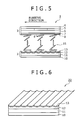
- FIG. 6 is a perspective view showing a TFT array substrate of a liquid crystal display panel applied to an Embodiment 2 of the present invention in contrast to FIG. 2 .
- this TFT array substrate 22 in place of the surface shape of the insulating film 11, the surface shape of the electrode 12 is formed in a groove shape while the shape of the face electrode 12 on which the orientation film 13 is produced is formed in a groove shape.
- the liquid crystal display panel of the present embodiment is formed similarly to the liquid crystal display panel 1 of the Embodiment 1 except the working of the groove shapes.
- the insulating film 11 is formed with a fixed film thickness on the glass substrate 10 in a similar manner as described hereinabove in connection with the Embodiment 1. Further, after a film of ITO, aluminum, silver or the like is formed subsequently, photosensitive resist is patterned into a groove shape by a photolithography method and then a wet etching process or a dry etching process is carried out to form a groove shape on the electrode 12. It is to be noted that the configuration shown in FIG. 6 may be applied to the CF substrate side similarly as in the description of the Embodiment 1.
- the surface shape of the electrode 12 is set to a groove shape and the shape of the face on which the orientation film is formed is set to a groove shape in place of the surface structure of the insulating film as in the case of the present embodiment, effects similar to those of the Embodiment 1 can be obtained.
- FIG. 7 is a perspective view showing a TFT array substrate of a liquid crystal display panel applied to a liquid crystal display apparatus of an Embodiment 3 of the present invention in contrast to FIG. 2 .
- This TFT array substrate 32 is configured such that, in place of the surface shape of the insulating film 11, the surface shape of the glass substrate 10 which is an insulating substrate is formed directly as a groove shape and the shape of the face of the glass substrate 10 on which the orientation film 13 is produced is formed in a groove shape.
- the liquid crystal display panel of the present embodiment is formed similarly to the liquid crystal display panel 1 of the Embodiment 1 except that it is different in terms of working of the groove shapes. It is to be noted that, although, in the example of FIG. 7 , the insulating film is omitted, an insulating film may be provided as occasion demands.
- the TFT array substrate 32 after photosensitive resist on the front face of the glass substrate 10 is patterned into grooves by a photolithography method, a wet etching process or a dry etching process is carried out to work the front face of the glass substrate 10 into a groove shape. Thereafter, the electrode 12 and the orientation film 13 are produced successively. It is to be noted that the configuration shown in FIG. 7 may be applied to the CF substrate side similarly as in the description of the Embodiment 1.
- the surface shape of the insulating substrate is set to a groove shape and the shape of the face on which the orientation film is produced is set to a groove shape as in the present embodiment in placed of the surface shape of the insulating film, effects similar to those of the Embodiment 1 can be achieved.
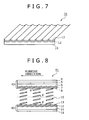
- FIG. 8 is a sectional view showing a liquid crystal display panel applied to a liquid crystal display apparatus of an Embodiment 4 of the present invention in contrast to FIG. 1 .
- a liquid crystal display panel 41 of the present embodiment is configured similarly to the liquid crystal display panels of the Embodiment 1 to the Embodiment 3 except that the grooves M formed on a TFT array substrate 42 have a different sectional shape and that a groove shape similar to that of the TFT array substrate 42 is formed also on a CF substrate 43 side.
- the surface shape of the insulating films 6 and 11 is a groove shape similarly as in the Embodiment 1.
- the sectional shape of the TFT array substrate 42 in a direction transverse to the grooves M is formed in an asymmetric shape with respect to the apex of each groove M. Consequently, the liquid crystal display panel 41 controls the tilt angle ⁇ of liquid crystal molecules 15 on the surface of the TFT array substrate 42 to an angle determined by the asymmetric shape.
- the TFT array substrate 42 has a groove shape formed such that the grooves M have a sawtooth sectional shape and consequently a rib of a triangular sectional shape defined by a pair of inclined faces M1 and M2 is successively repeated at a predetermined pitch. Consequently, in the TFT array substrate 42, the angles ⁇ 1 and ⁇ 2 defined by a pair of inclined faces M1 and M2 with respect to a plane H parallel to the surface of the glass substrate 10 are set to different angles to control the tilt angle of the liquid crystal molecules 15.
- the sectional shape of the grooves is not limited to that in the case wherein it is a sawtooth shape, but in a word, the grooves can be formed in an asymmetric shape to control the tilt angle of the liquid crystal molecule 15 variously such as where, for example, the apex of each groove M is displaced to one side to obtain an asymmetric shape.
- the grooves M are formed such that the pitch P is 1 [ ⁇ m] and the height H is 200 [nm] while the angle ⁇ 1 is set to 3 degrees.
- the orientation film 13 was formed by applying a polyimide-based material and then baking for 75 minutes at a temperature of 200 degrees so as to have a thickness of 50 [nm].
- the orientation film 8 was formed after a groove shape same as that of the TFT array substrate 42 was formed.
- the liquid crystal display panel 41 of the present embodiment is formed by pasting the TFT array substrate 42 and the CF substrate 43 together by means of a sealing material and then injecting nematic liquid crystal having positive dielectric constant anisotropy into the gap between the TFT array substrate 42 and the CF substrate 43.
- the orientation direction of the liquid crystal molecule 15 was confirmed in a similar manner to that described hereinabove in connection with the Embodiment 1, it was confirmed that the liquid crystal molecules 15 were directed in a direction perpendicular to the direction in which the groove M extended. Further, it was confirmed that, if the TFT array substrate 42 and the CF substrate 43 were pasted together such that the direction in which the sawtooth shapes of the TFT array substrate 42 successively appeared and the direction in which the sawtooth shapes of the CF substrate 43 successively appeared were opposite to each other, then homogeneous orientation was obtained.
- FIG. 10 is a schematic view where a voltage is applied to the liquid crystal display panel 41.
- the orientation of liquid crystal molecules does not vary in the proximity of the interface of the TFT array substrate 42 and the CF substrate 43, and as the distance from the interface increases, the tilt angle of liquid crystal molecules 15 gradually increases until the tilt angle becomes approximately 90 degrees and exhibits a maximum value at a central portion between the TFT array substrate 42 and the CF substrate 43. It was confirmed that retardation substantially equal to that of liquid crystal cells wherein both of the TFT array substrate and the CF substrate were subjected to a rubbing process was measured on the liquid crystal display panel 41 in this state, and consequently, the liquid crystal display panel 41 assured sufficient anchoring strength.
- the tilt angle of liquid crystal molecules can be controlled in various manners by forming the sectional shape in a direction perpendicular to the grooves in an asymmetric shape with respect to the apex of each groove.
- FIG. 11 is a sectional view showing a liquid crystal display panel applied to a liquid crystal display apparatus of an Embodiment 5 of the present invention in contrast to FIG. 1 .
- a liquid crystal display panel 51 of the present embodiment is formed in the same configuration as the liquid crystal display panel 1 of the Embodiment 1 to the Embodiment 3 except that nematic liquid crystal having negative dielectric constant anisotropy is injected between the TFT array substrate 2 and the CF substrate 3 in place of nematic liquid crystal having positive dielectric constant anisotropy and that an orientation film which induces homeotropic orientation is used.
- the surface shape of the insulating film 11 is a groove shape similarly as in the Embodiment 1.
- liquid crystal molecules 55 were oriented to a thicknesswise direction of the liquid crystal display panel 51 and have homeotropic orientation.
- FIG. 12 is a schematic view where a voltage is applied to the liquid crystal display panel 51.
- the orientation of the liquid crystal molecules 55 does not vary in the proximity of an interface of the TFT array substrate 2 and the CF substrate 3, and as the distance from the interface increases, the tilt angle of liquid crystal molecules 55 gradually decreases until the tilt angle becomes approximately 0 degree and exhibits a minimum value at a central portion between the TFT array substrate 2 and the CF substrate 3. It was confirmed that the orientation direction of the liquid crystal molecules 55 where the tilt angle was approximately 0 degree was a direction perpendicular to the extension direction of the grooves and the tilt direction depends upon the rubbing direction.
- FIGS. 13 and 14 are sectional views showing a liquid crystal display panel applied to a liquid crystal display apparatus of an Embodiment 6 of the present invention in contrast to FIGS. 8 and 10 .
- a liquid crystal display panel 61 of the present embodiment is formed in a same configuration as that of the liquid crystal display panel 41 of the Embodiment 4 except that nematic liquid crystal having negative dielectric constant anisotropy is injected between the TFT array substrate 42 and the CF substrate 43 in place of nematic liquid crystal having positive dielectric constant anisotropy and that an orientation film which induces homeotropic orientation is used.
- the surface shape of the insulating films 6 and 11 is a groove shape similarly as in FIG. 8 .
- the liquid crystal molecules 55 were oriented in a thicknesswise direction of the liquid crystal display panel 61 and have homeotropic orientation. Further, it was confirmed that, in the proximity of the interface of the TFT array substrate 42 and the CF substrate 43, the liquid crystal molecules 55 were oriented in a vertical direction with respect to the surface of the glass substrate 4 or 10 at a tilt angle in a direction determined by the groove shape.
- the orientation of the liquid crystal molecules 55 does not vary in the proximity of the interface of the TFT array substrate 42 and the CF substrate 43, and as the distance from the interface increases, the tilt angle of the liquid crystal molecules 55 decreases until it becomes almost 0 degree and is in the minimum at a central portion between the TFT array substrate 42 and the CF substrate 43. It was confirmed that the orientation direction of the liquid crystal molecules 55 at which the tilt angle became approximately 0 degree was a direction perpendicular to the extension direction of the grooves.
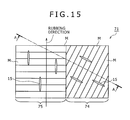
- FIG. 15 is a plan view showing a schematic configuration of one pixel of a liquid crystal display panel applied to a liquid crystal display apparatus of an Embodiment 7 of the present invention
- FIG. 16 is a detailed sectional view taken along line A-A showing a liquid crystal display panel 71. It is to be noted that FIG. 15 is a view showing grooves M formed on a CF substrate 73 together with liquid crystal molecules 15.
- the liquid crystal display panel 71 is of the half-transmission type and includes a reflection display portion 74 and a transmission display portion 75 provided in one pixel.
- a quarter-wave plate 76, a half-wave plate 77 and a polarizing plate 78 are successively provided on a lower face of a TFT array substrate 72.
- a quarter-wave plate 79, a half-wave plate 80 and a polarizing plate 81 are successively provided on an upper face of the CF substrate 73.
- this TFT array substrate 72 After the insulating film 11, electrode 12 and orientation film 13 are formed successively on the glass substrate 10, a rubbing process is carried out to provide orientation ability to the orientation film 13.
- the reflection display portion 74 concave and convex shapes are formed on the insulating film 11 so as to disperse incoming light while the front side faces of the electrode 12 and orientation film 13 are formed in concave and convex shapes.
- the color filter 5, insulating film 6, electrode 7 and orientation film 8 are successively formed on the glass substrate 4, and the shape of the face on which the orientation film 8 is formed is formed as a groove shape to provide orientation ability to the orientation film 8 similarly to the TFT array substrate described hereinabove in connection with the Embodiment 1 to the Embodiment 4.
- the reflection display portion 74 and the transmission display portion 75 are optically designed so as to have the same axial angle and retardation, and the gap between the TFT array substrate 72 and the CF substrate 73 is set to the same distance.
- the transmission display portion 75 the extension direction of the grooves M formed on the CF substrate 73 is set so as to coincide with the rubbing direction of the TFT array substrate 72.
- the reflection display portion 74 the extension direction of the grooves M formed on the CF substrate 73 is set so as to be inclined obliquely with respect to the rubbing direction of the TFT array substrate 72.
- the present liquid crystal display panel 71 can assure different orientation in one pixel readily by means of the reflection display portion 74 and the transmission display portion 75 without provision of an offset in the gap between TFT array substrate 72 and the CF substrate 73.
- the transmission display portion 75 has homogeneous orientation and the reflection display portion 74 has 50-degree twisted orientation.
- the twist angle of the reflection display portion 74 is not limited to 50 degrees, but the liquid crystal display panel 71 can be configured such that the twist angle is within a range of 40 degrees to 70 degrees.
- the extension direction of the grooves M on the reflection display portion 74 is set so as to have an angle of 50 degrees with respect to the extension direction of the grooves M on the transmission display portion 75, this angle can be used within a range from 40 degrees to 70 degrees in practical use.
- orientation ability is provided to an orientation film through a groove shape on the CF substrate 73
- orientation ability may be provided to an orientation film through a groove shape on the TFT array substrate 72.
- orientation ability may be provided to an orientation film through a groove shape on both of the CF substrate 73 and the TFT array substrate 72.
- the extension direction of the grooves in the reflection display portion can be inclined with respect to the extension direction of the grooves in the transmission display portion on both or one of the CF substrate 73 and the TFT array substrate 72.
- the sectional shape of the grooves may be set to an asymmetric shape to control the tilt angle as described hereinabove in connection to the Embodiment 4.
- liquid crystal having negative dielectric constant anisotropy may be applied in place of liquid crystal having positive dielectric constant anisotropy.
- the inclination of the grooves M may be made different between the transmission display portion and the reflection display portion for each of sub pixels which form one pixel so that the optical characteristic is optimized for each sub pixel.
- a configuration wherein an optical characteristic is optimized for each sub pixel in this manner can be applied not only to a semi-transmission type liquid crystal display panel but also to a transmission type liquid crystal display panel and a reflection type liquid crystal display panel.
- the gap between the CF substrate and the TFT array substrate is optimized for the green color
- the distance of the gap is excessively great for the blue color and the distance of the gap is excessively small for the red color.
- an optical characteristic can be optimized for each sub pixel.
- FIG. 17 is a perspective view showing an example of a configuration of a TFT array substrate 92 applied to a liquid crystal display apparatus of an Embodiment 8 of the present invention in contrast to FIG. 2 .
- the TFT array substrate 92 grooves M are formed such that equal to or more than a fixed number of those grooves M which have a fixed pitch P may not successively appear. More particularly, the TFT array substrate 92 is set such that the pitch P varies at random along successive grooves M. Consequently, the TFT array substrate 92 is set such that successive grooves M do not function as diffraction gratings.
- the liquid crystal display panel of the present embodiment is formed in a configuration same as that of the embodiments described hereinabove except that the setting of the pitch P of the TFT array substrate 92 is different.
- the periodical grooves M function as diffraction gratings, and rainbow-colored interference fringes are observed and the picture quality is deteriorated significantly.
- the orientation film contacts with liquid crystal whose refractive index is approximately 1.5, although rainbow-colored interference fringes do not appear as many as those where the grooves M are exposed to the air, they appear since the refractive index of the transparent electrode of ITO or the like is substantially equal to 2.
- rainbow-colored interference fringes become marked in the case of a reflection type liquid crystal display panel.
- the pitch is varied so that equal to or more than a fixed number of grooves having a fixed pitch do not appear successively, appearance of rainbow-colored interference fringes can be prevented to prevent deterioration of the picture quality.
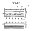
- FIG. 18 is a sectional view showing a liquid crystal display panel applied to a liquid crystal display apparatus of an Embodiment 9 of the present invention in contrast to FIG. 16 .
- a liquid crystal display panel 101 of the present embodiment like components to those in the embodiments described hereinabove are denoted by like reference characters, and overlapping description is suitably omitted herein.
- the present liquid crystal display panel 101 is of the transmission type, and a quarter-wave plate 76, a half-wave plate 77 and a polarizing plate 78 are successively provided on a lower face of a TFT array substrate 102.
- a half-wave plate 80 and a polarizing plate 81 are successively provided on an upper face of a CF substrate 103 to form a quarter-wave plate on the glass substrate 4 of the CF substrate 103.
- the CF substrate 103 includes an insulating film 105 and an orientation film 106 successively formed on the glass substrate 4.
- a face of the CF substrate 103 on which the orientation film 106 is formed is formed in a groove shape in a similar manner to that described hereinabove with reference to the Embodiment 1 to the Embodiment 3 described hereinabove, and a high-molecular material is applied with a fixed film thickness in such a manner as to cover the groove shape. Thereafter, heating and cooling steps are applied to form the orientation film 106.
- a nematic liquid crystal material for a phase difference plate is applied to the CF substrate 103, and liquid crystal molecules 108 which form the nematic liquid crystal material are oriented by the orientation film 106 in a direction perpendicular to the extension direction of the grooves M formed on the orientation film 106.
- Ultraviolet rays are irradiated on the CF substrate 103 in this state to solidify the liquid crystal material to form a quarter-wave plate 107 of the A plate on the glass substrate 4.
- the color filter 5, insulating film 6, electrode 7 and orientation film 8 are successively formed on the CF substrate 103, and orientation ability is provided to the orientation film 8 by a rubbing method.
- an insulating film 11, an electrode 12 and an orientation film 13 are successively formed on the glass substrate 10, and orientation ability is applied to the orientation film 13 by a rubbing method.
- the surface shape of the glass substrate 4 may be worked into a groove shape as described hereinabove in connection with the Embodiment 3.
- the overall thickness can be reduced.
- the thickness of the quarter-wave plate 107 can be set to several [ ⁇ m] or less, and the overall thickness can be reduced significantly when compared with that of the related art apparatus and methods.
- the extension direction of the grooves can be varied within one pixel to optimize an optical characteristic for each sub pixel of each color and further within one pixel.
- FIG. 19 is a sectional view showing a liquid crystal display panel applied to a liquid crystal display display of an Embodiment 10 of the present invention in contrast to FIGS. 16 and 18 .
- a liquid crystal display panel 111 of the present embodiment like components to those in the embodiments described hereinabove are denoted by like reference characters, and overlapping description is suitably omitted herein.
- the present liquid crystal display panel 111 is of the semi-transmission type and includes pixels each formed from a reflection display portion 74 and a transmission display portion 75.
- the TFT array substrate 72 is formed in a configuration same as that of the liquid crystal display panel 71 of FIG. 16 , and a quarter-wave plate 76, a half-wave plate 77 and a polarizing plate 78 are successively provided on the TFT array substrate 72.
- a half-wave plate 80 and a polarizing plate 81 are successively provided on an upper face of a CF substrate 113.
- the CF substrate 113 includes an insulating film 105, an orientation film 106, a quarter-wave plate 107 and a color filter 5 formed on the glass substrate 4 similarly to the CF substrate 103 of the liquid crystal display panel 101.
- an insulating film 6 is deposited on the CF substrate 113, for example, a technique of photolithography is applied to selectively remove the CF substrate 113 on the transmission display portion 75 side thereby to form an offset between the transmission display portion 75 and the reflection display portion 74.
- the electrode 7 and the orientation film 8 are successively formed, and orientation ability is provided to the orientation film 8 by a rubbing method.
- the offset between the transmission display portion and the reflection display portion is not restrictively provided on the counter CF substrate, but may be provided on the TFT array substrate side or may be provided on both of them.
- the surface shape of the glass substrate 4 may be worked into a groove shape as described hereinabove in connection with the Embodiment 3.
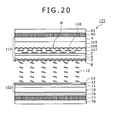
- FIG. 20 is a sectional view showing a liquid crystal display panel applied to a liquid crystal display apparatus of an Embodiment 11 of the present invention in contrast to FIGS. 16 to 19 .
- a liquid crystal display panel 121 of the present embodiment like components to those in the embodiments described hereinabove are denoted by like reference characters, and overlapping description is suitably omitted herein.
- the present liquid crystal display panel 121 is of the transmission type, and a TFT array substrate 102 is formed in a configuration same as that of the liquid crystal display panel 101 of FIG. 18 and a quarter-wave plate 76, a half-wave plate 77 and a polarizing plate 78 are successively provided on the TFT array substrate 102.
- a CF substrate 123 includes an insulating film 105, an orientation film 106, a quarter-wave plate 107 and a color filter 5 formed on the glass substrate 4 similarly to the CF substrate 103 of the liquid crystal display panel 101. Thereafter, an insulating film 6 is deposited on the CF substrate 123, and the surface shape of the insulating film 6 is worked into a groove shape and an electrode 7 and an orientation film 8 are formed so that orientation ability is provided to the orientation film 8 by the groove shape.
- the surface shape of the glass substrate 4 is worked into a groove shape as described hereinabove in connection with the Embodiment 3.
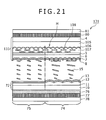
- FIG. 21 is a sectional view showing a liquid crystal display panel applied to a liquid crystal display apparatus of the Embodiment 12 of the present invention in contrast to FIGS. 16 to 19 .
- a liquid crystal display panel 131 of the present embodiment like components to those in the embodiments described hereinabove are denoted by like reference characters, and overlapping description is suitably omitted herein.
- the present liquid crystal display panel 131 is of the semi-transmission type, and one pixel is formed from a reflection display portion 74 and a transmission display portion 75.
- the TFT array substrate 72 is formed in a configuration same as that of the liquid crystal display panel 71 of FIG. 16 , and a quarter-wave plate 76, a half-wave plate 77 and a polarizing plate 78 are successively provided on the TFT array substrate 72.
- a CF substrate 133 includes a glass substrate 4, an insulating film 105, an orientation film 106, a quarter-wave plate 107 and a color filter 5 formed on the glass substrate 4 similarly to the CF substrate 103 of the liquid crystal display panel 101. Thereafter, an insulating film 6 is deposited on the CF substrate 133, and the surface shape of the insulating film 6 is worked into a groove shape and an electrode 7 and an orientation film 8 are formed so that orientation ability is provided to the orientation film 8 by the groove shape.
- the CF substrate 133 is formed from the reflection display portion 74 and the transmission display portion 75 such that the gap may be equal similarly to the liquid crystal display panel 71 described hereinabove with reference to FIG. 16 . Further, the extension direction of the grooves M formed on a lower face of the orientation film 8 may be a different direction.
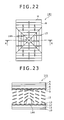
- FIG. 22 is a plan view showing a liquid crystal display panel applied to a liquid crystal display apparatus of an Embodiment 13 of the present invention in contrast to FIG. 15
- FIG. 23 is a detailed sectional view showing a liquid crystal display panel 141 taken along line A-A
- FIG. 24 is a sectional view showing a state wherein a voltage is applied to an electrode in contrast to FIG. 23 .
- like components to those in the embodiments described hereinabove are denoted by like reference characters, and overlapping description is suitably omitted herein.
- orientation ability is provided by the groove shape. It is to be noted that, upon production of the groove shape, any of the Embodiment 1 to Embodiment 3 may be applied.
- grooves M are formed on the CF substrate and the TFT array substrate such that, in upward and downward directions from the center of one pixel, each of them extends horizontally while, in leftward and rightward directions from the center of one pixel, each of them extends vertically, whereby the grooves M are formed in a quadrangular shape centered at the center of a pixel.
- the liquid crystal display panel 141 is set such that the grooves M are formed in a symmetrical shape in various directions with respect to the center of one pixel and, in the upward and downward directions from the center of one pixel, the liquid crystal molecules 15 are oriented in the upward and downward directions while, in leftward and rightward directions from the center of one pixel, the liquid crystal molecules 15 are oriented horizontally such that the liquid crystal molecules 15 are directed to the center of the pixel.
- liquid crystal display panel 141 a projection 144 of a quadrangular pyramid shape is formed at the center of one pixel on the TFT array substrate such that it projects toward the CF substrate. Consequently, the liquid crystal display panel 141 is set such that the tilt angle decreases as the distance from the center of one pixel increases toward the periphery of the pixel. Consequently, in the liquid crystal display panel 141, the phase of light incoming to the liquid crystal cell from the same polar angle is substantially equal even if the azimuth angle differs, and the liquid crystal display panel 141 is formed such that the viewing angle is expanded.
- the viewing angle can be expanded by forming the grooves M in a symmetrical shape in various directions with reference to the center of one pixel. It is to be noted that one pixel may be divided into a plurality of sub pixels to form the grooves in a symmetrical shape with reference to the center of each sub pixels.
- FIG. 25 is a plan view showing a liquid crystal display panel applied to a liquid crystal display apparatus of the Embodiment 14 of the present invention in contrast to FIG. 22 .
- the present liquid crystal display panel 151 is formed in a configuration same as that of the liquid crystal display panel 141 of the Embodiment 13 except that grooves M are formed concentrically. Consequently, a conical projection is provided in place of the projection of a quadrangular pyramid shape at the center of one pixel.
- FIGS. 26 and 27 are plan views showing a liquid crystal display panel applied to a liquid crystal display apparatus of an Embodiment 15 of the present invention in contrast to FIGS. 23 and 24 .
- the present liquid crystal display panel 161 is formed in a configuration similar to those of the Embodiment 13 and the Embodiment 14 except that the projection of a quadrangular pyramid shape or a conical shape is omitted and the grooves M are formed in a sectional shape described hereinabove in connection with the Embodiment 4.
- the pitch of the grooves is varied at random to prevent rainbow-colored interference fringes
- the groove width may be varied in the extension direction of the grooves to prevent rainbow-colored interference fringes.
- a quarter-wave plate is produced on a CF substrate
- the present invention is not limited to this, but can be applied widely also where a half-wave plate, a polarizing plate and other various phase difference plates are produced on the CF substrate. Further, a phase difference plate may be produced on the TFT array substrate side.
- a nematic liquid crystal material is used to produce a phase different plate of the A plate
- the present invention is not limited to this, but a liquid crystal material of hybrid orientation may be used to produce a phase difference plate of the O plate and various liquid crystal materials such as smectic, cholesteric and discotic liquid crystals can be applied widely.
- a phase difference plate of the C plate may be formed by forming an orientation film for inducing vertical orientation and homeotropically orienting liquid crystal molecules.
- grooves are formed uniformly in one pixel to produce a phase difference plate
- the present invention is not limited to this, but the extension direction of grooves may be varied in one pixel to optimize the optical characteristic for each sub pixel of each color and further in one pixel.
- phase difference plate is produced on the liquid crystal side of the insulating substrate
- the present invention is not limited to this, but a phase difference plate may be produced on the opposite side to this.
- the extension direction of grooves is varied within one pixel
- the present invention is not limited to this, but the extension direction of grooves may be varied within one sub pixel.
- the techniques of the Embodiment 1 to the Embodiment 4 are selectively applied suitably to form the shape of a face on which an orientation film is formed as a groove shape
- the present invention is not limited to this, but any other one of the techniques of the Embodiment 1 to the Embodiment 4 may be applied in place of the techniques described hereinabove in connection with the embodiments within a range within which the configuration described hereinabove in connection with the embodiment is not damaged.
- a glass plate is used as an insulating substrate
- the present invention is not limited to this, but various insulating substrates such as a plastic substrate can be applied widely.
- an orientation film is coated on a face on which a groove extending in a predetermined direction is repetitively formed in a direction perpendicular to the predetermined direction and high-molecular chains of the orientation film are adjusted to the direction perpendicular to the grooves
- an orientation film whose high-molecular chains are adjusted to the direction in which the grooves extend may be applied.
- an orientation film is coated on a face on which a groove extending in a predetermined direction is repetitively formed in a direction perpendicular to the predetermined direction and liquid crystal molecules are adjusted to the direction perpendicular to the grooves
- an orientation film whose liquid crystal molecules are adjusted to the direction in which the grooves extend may be applied.
- the present invention can be applied to a liquid crystal display panel of a liquid crystal mode such as TN, ECB, STN and IPS modes.
- a liquid crystal mode such as TN, ECB, STN and IPS modes.
Abstract
Description
- This invention relates to a liquid crystal display panel and a fabrication method for a liquid crystal display apparatus and can be applied to a liquid crystal mode such as TN (Twisted Nematic), ECB (Electrically Controlled birefringence), STN (Super Twisted Nematic) and IPS (In-Plane Switching) modes. The present invention makes it possible to assure high productivity and sufficient anchoring strength and picture quality when compared with related art apparatus and methods by providing a lower face of an orientation film with a groove shape to provide orientation ability to the orientation film.
- Conventionally, in liquid crystal display panels of various liquid crystal modes such as TN, ECB, STN and IPS modes, liquid crystal molecules are oriented to a fixed direction by an orientation process, and various techniques have been proposed for this orientation process.
- Here, a rubbing method which is one of such orientation processes is a method used most frequently, and orientation ability is applied to an orientation film formed from a high molecular film made of polyimide or the like by forming the orientation film on transparent electrodes and rubbing the orientation film in a fixed direction by means of a roller having a cloth or the like attached to the surface thereof. However, with the rubbing method, there is the possibility that rubbing waste may stick to and pollute the surface of the orientation film, and also there is the possibility that TFTs (thin film transistors) may be broken down by generation of static electricity.
- A grating method which is an orientation processing method used in place of the rubbing method works an orientation film on the surface of a substrate to form gratings (grooves) and makes use of elastic deformation by the gratings to orient liquid crystal molecules. In the grating method, liquid crystal molecules are oriented in a parallel direction along the gratings in which elastic free energy is most stable.
- In regard to this grating method, a method has been proposed in M. Nakamura et al. J. Appl. Phys. 52, 210 (1981) wherein light is irradiated upon photosensitive polymer which forms an orientation film to form gratings linearly at fixed distances. Meanwhile, in the official gazette of Japanese Patent Laid-Open No.
Hei 11-218763 2000-105380 - It is known that, according to this grating method, anchoring energy can be controlled by adjustment of the pitch and the height of the gratings (Y. Ohta et al., J. J. Appl. Phys., 43, 4310 (2004)).
- Further, in regard to the grating method, also a method is proposed wherein the orientation regulating force which the orientation film itself of polyimide or the like has is utilized to improve anchoring strength. In particular, in the official gazette of Japanese Patent Laid-Open No.
Hei 5-88177 Hei 8-114804 Hei 3-209220 - Incidentally, according to the grating method, pollution of the orientation film surface or generation of static electricity by the rubbing method can be prevented.
- However, where only an elastic deformation effect according to the grating method is merely utilized to orient liquid crystal molecules, in order to achieve anchoring strength of a level equal to that of the rubbing method, it is necessary to make the ratio T (= H/P) between the pitch P and the height H of the grooves sufficiently high. In particular, according to Y. Ohta et al., J. J. Appl. Phys., 43, 4310 (2004), in order to obtain a level of azimuth angle anchoring strength (approximately 1 × 10⁻⁴ [J/m2]) substantially equal to that of an orientation film produced through a rubbing process, it is necessary to make the ratio T between the pitch P and the height H of the grooves equal to 1 or more. Accordingly, since the pitch of gratings estimated to be practically used is 1 [µm] or more, in order to assure sufficient azimuth angle anchoring strength, where only the elastic deformation effect is utilized to orient liquid crystal molecules, it is necessary to make the depth of gratings equal to 1 [µm] or more. Here, in a liquid crystal display panel, since the cell gap is approximately 3 to 4 [µm], if the depth of the gratings is 1 [µm] or more, then periodic concaves and convexes having a depth of 1 [µm] or more are formed on a panel face, and the retardation varies within the panel face and it is difficult to sufficiently assure the contrast ratio. Further, where the productivity is taken into consideration, it is desired to make the depth of gratings smaller than 1 [µm] to assure sufficient anchoring strength.
- Consequently, where only the elastic deformation effect is merely utilized to orient liquid crystal molecules by a grating method, there is a problem that it is still insufficient in practical use in terms of assurance of sufficient anchoring strength.
- In the meantime, according to the method wherein the orientation regulating force which the orientation film material itself has is utilized to improve the anchoring strength, it is estimated that, even if the depth of gratings is made smaller than 1 [µm], sufficient anchoring strength is assured.
- However, the technique disclosed in the official gazette of Japanese Patent Laid-Open No.
Hei 5-88177 Hei 8-114804 Hei 3-209220 - Patent Document 1: official gazette of Japanese Patent Laid-Open No.
Hei 11-218763 - Patent Document 2: official gazette of Japanese Patent Laid-Open No.
2000-105380 - Patent Document 3: official gazette of Japanese Patent Laid-Open No.
Hei 5-88177 - Patent Document 4: official gazette of Japanese Patent Laid-Open No.
Hei 8-114804 - Patent Document 5: official gazette of Japanese Patent Laid-Open No.
Hei 3-209220 - Non-Patent Document 1: M. Nakamura et al. J. Appl. Phys. 52, 210 (1981)
- Non-Patent Document 2: Y. Ohta et al., J. J. Appl. Phys., 43, 4310 (2004)
- The present invention has been made taking the foregoing into consideration and provides a liquid crystal display panel and a fabrication method for a liquid crystal display panel which solve such problems as described above at once and which are high in productivity when compared with the related art apparatus and methods and can assure sufficient anchoring strength and picture quality.
- In order to solve the subject described above, the invention of
claim 1 is applied to a liquid crystal display panel wherein liquid crystal is held between two substrates opposing to each other, wherein at least one of the two substrates is formed such that the shape of a face thereof on which an orientation film is produced is a groove shape wherein a groove extending in a predetermined direction is formed repetitively in a direction perpendicular to the predetermined direction, and the groove shape is covered with a high-molecular film to form the orientation film whose high-molecular chains are adjusted to the perpendicular direction. - The invention of claim 18 is applied to a liquid crystal display panel wherein liquid crystal is held between two substrates opposing to each other, wherein at least one of the two substrates is formed such that the shape of a face thereof on which an orientation film is produced is a groove shape wherein a groove extending in a predetermined direction is formed repetitively in a direction perpendicular to the predetermined direction, and the groove shape is covered with a high-molecular film to form the orientation film which orients molecules of the liquid crystal to the perpendicular direction.
- The invention of claim 34 is applied to a liquid crystal display panel wherein liquid crystal is held between two substrates opposing to each other, wherein at least one of the two substrates includes an insulating substrate, and an orientation film for a phase difference plate having a face on which a groove extending in a predetermined direction is formed repetitively in a direction perpendicular to the predetermined direction and which is covered with a high-molecular film such that high-molecular chains are adjusted to the perpendicular direction and a phase difference plate formed from liquid crystal oriented in a direction determined by the orientation film for the phase difference plate are successively formed on the insulating substrate.
- The invention of claim 35 is applied to a liquid crystal display panel wherein liquid crystal is held between two substrates opposing to each other, wherein at least one of the two substrates includes an insulating substrate, and an orientation film for a phase difference plate having a face on which a groove extending in a predetermined direction is formed repetitively in a direction perpendicular to the predetermined direction and which is covered with a high-molecular film and a phase difference plate formed from liquid crystal whose molecules are oriented to the perpendicular direction are successively formed on the insulating substrate.
- The invention of claim 36 is applied to a fabrication method for a liquid crystal display panel wherein liquid crystal is held between two substrates opposing to each other, wherein the fabrication method for a liquid crystal display panel comprises a groove working step of working at least one of the two substrates such that the shape of a face thereof on which an orientation film is to be produced is a groove shape wherein a groove extending in a predetermined direction is formed repetitively in a direction perpendicular to the predetermined direction, and an orientation film production step of covering the groove shape with a high-molecular film to form the orientation film whose high-molecular chains are adjusted to the perpendicular direction.
- The invention of claim 37 is applied to a fabrication method for a liquid crystal display panel wherein liquid crystal is held between two substrates opposing to each other, wherein the two substrates include an electrode and an orientation film successively formed on an insulating substrate, and the fabrication method for a liquid crystal display panel comprises a groove working step of working at least one of the two substrates such that the shape of a face thereof on which the orientation film is to be produced is a groove shape wherein a groove extending in a predetermined direction is formed repetitively in a direction perpendicular to the predetermined direction, and an orientation film production step of covering the groove shape with a high-molecular film to form the orientation film which orients molecules of the liquid crystal to the perpendicular direction.
- The invention of claim 38 is applied to a fabrication method for a liquid crystal display panel wherein liquid crystal is held between two substrates opposing to each other, wherein at least one of the two substrates includes an orientation film for a phase difference plate and a phase difference plate successively provided on a transparent substrate, and the fabrication method for a liquid crystal display panel comprises a groove working step of working the one substrate such that the shape of a face thereof on which the orientation film is to be produced is a groove shape wherein a groove extending in a predetermined direction is formed repetitively in a direction perpendicular to the predetermined direction, an orientation film production step of covering the groove shape with a high-molecular film to form the orientation film for a phase difference plate whose high-molecular chains are adjusted to the perpendicular direction, a liquid crystal arranging step of arranging liquid crystal on the orientation film of the phase difference plate, and a solidifying step of solidifying the liquid crystal.
- The invention of claim 39 is applied to a fabrication method for a liquid crystal display panel wherein liquid crystal is held between two substrates opposing to each other, wherein at least one of the two substrates includes an orientation film and a phase difference plate successively provided on a transparent substrate, and the fabrication method for a liquid crystal display panel comprises a groove working step of working the one substrate such that the shape of a face thereof on which the orientation film is to be produced is a groove shape wherein a groove extending in a predetermined direction is formed repetitively in a direction perpendicular to the predetermined direction, an orientation film production step of covering the groove shape with a high-molecular film to form the orientation film for the phase difference plate, a liquid crystal arranging step of arranging liquid crystal, whose molecules are oriented to the perpendicular direction, on the orientation film of the phase difference plate, and a solidifying step of solidifying the liquid crystal.
- The invention of claim 40 is applied to a liquid crystal display panel wherein liquid crystal is held between two substrates opposing to each other, wherein at least one of the two substrates is formed such that the shape of a face thereof on which an orientation film is produced is a groove shape wherein a groove extending in a predetermined direction is formed repetitively in a direction perpendicular to the predetermined direction, and the groove shape is covered with a high-molecular film to form the orientation film whose high-molecular chains are adjusted to the predetermined direction.
- The invention of
claim 41 is applied to a liquid crystal display panel wherein liquid crystal is held between two substrates opposing to each other, wherein at least one of the two substrates is formed such that the shape of a face thereof on which an orientation film is produced is a groove shape wherein a groove extending in a predetermined direction is formed repetitively in a direction perpendicular to the predetermined direction, and the groove shape is covered with a high-molecular film to form the orientation film which orients molecules of the liquid crystal to the perpendicular direction. - In the orientation film formed such that a groove shape wherein a groove extending in a predetermined direction is formed repetitively in a perpendicular direction is covered with a high-molecular film according to the configuration of
claim 1, 18, 36 or 37, high molecules are adjusted to the direction perpendicular to the extension direction of the grooves by expansion and contraction by heat treatment upon production thereby to assure orientation ability. Consequently, according to the configuration ofclaim 1, 18, 36 or 37, high productivity can be assured to produce an orientation film by simple and easy steps. With the orientation ability assured in this manner here, even if the depth of the grooves is not made deep, liquid crystal molecules can be oriented by sufficient anchoring strength, and the problems of the related art apparatus and methods can be solved at a time to assure high productivity when compared with that of the related art apparatus and methods and assure sufficient anchoring strength and picture quality. - In the orientation film for a phase difference plate formed such that a face thereof on which a groove extending in a predetermined direction is formed repetitively in a perpendicular direction is covered with a high-molecular film according to the configuration of claim 34, 35, 38 or 39, high molecules are adjusted to the direction perpendicular to the extension direction of the grooves by expansion and contraction by heat treatment upon production thereby to assure orientation ability. Consequently, according to the configuration of claim 34, 35, 38 or 39, high productivity can be assured to produce an orientation film by simple and easy steps. Further, the orientation film for a phase difference plate can be utilized to produce a phase difference plate.
- In the orientation film formed such that a groove shape wherein a groove extending in a predetermined direction is formed repetitively in a perpendicular direction is covered with a high-molecular film according to the configuration of
claim 40 or 41, high molecules are adjusted to the predetermined direction by expansion and contraction by heat treatment upon production thereby to assure orientation ability. Consequently, according to the configuration ofclaim 40 or 41, high productivity can be assured to produce an orientation film by simple and easy steps. With the orientation ability assured in this manner here, even if the depth of the grooves is not made deep, liquid crystal molecules can be oriented by sufficient anchoring strength, and the problems of the related art apparatus and methods can be solved at a time to assure high productivity when compared with that of the related art apparatus and methods and assure sufficient anchoring strength and picture quality. Advantageous Effects - According to the present invention, the productivity is high when compared with that of the related art apparatus and methods, and sufficient anchoring strength and picture quality can be assured. Best Mode for Carrying Out the Invention
- In the following, embodiments of the present invention are described suitably with reference to the drawings.
-
FIG. 1 is a sectional view showing, in a partly enlarged scale, a liquidcrystal display panel 1 applied to a liquid crystal display apparatus of anEmbodiment 1 of the present invention. The liquid crystal display apparatus of the present embodiment is of the transmission type or of the reflection type, and a polarizing plate and so forth are provided on a front side face of the liquidcrystal display panel 1 which is the upper side inFIG. 1 or the like. In the transmission type, a backlight apparatus is provided on the rear face side of the liquidcrystal display panel 1 which is the lower side inFIG. 1 , but in the reflection type, a frontlight apparatus is provided on the front face side of the liquidcrystal display panel 1 which is the upper side inFIG. 1 . - The liquid
crystal display panel 1 includes liquid crystal sandwiched between aTFT array substrate 2 and aCF substrate 3. Here, theCF substrate 3 is produced by successively forming acolor filter 5, an insulatingfilm 6, anelectrode 7 in the form of a transparent electrode and anorientation film 8 on aglass substrate 4 which is a transparent insulating substrate. Here, although theelectrode 7 is usually formed by forming a film of ITO (Indium Tin Oxide) over an overall area, it may otherwise be formed by patterning for each pixel or for each sub pixel. Meanwhile, theorientation film 8 is produced by applying mixture of soluble polyimide and polyamic acid as a liquid crystal orientation material for inducing horizontal orientation by a printing method and baking the applied mixture for 75 minutes at a temperature of 200 degrees to form a polyimide thin film of a film thickness of 50 [nm] and then carrying out a rubbing process to provide orientation ability. It is to be noted that the direction of the rubbing process is the direction of an arrow mark in this figure and is a direction perpendicular to the extension direction of grooves M hereinafter described. - In contrast, the
TFT array substrate 2 is produced by forming TFTs or the like on aglass substrate 10 which is a transparent insulating substrate and forming an insulatingfilm 11 and then successively forming anelectrode 12 and anorientation film 13 on the insulatingfilm 11 as seen inFIG. 2 . - The
TFT array substrate 2 is formed such that the shape of a face thereof on which theorientation film 13 is produced is a groove shape wherein a groove extending linearly in a predetermined direction is formed repetitively in a direction perpendicular to the predetermined direction, and the groove shape is coated with a high-molecular film to form theorientation film 13. Further, in the present embodiment, the surface shape of the insulatingfilm 11 is formed in this groove shape such that the face on which theorientation film 13 is produced is formed in the groove shape. - Here, each of the grooves M has a cross sectional shape formed in a substantially arcuate shape of a symmetrical shape with respect to a vertex of the groove M. Further, each groove M is formed such that the pitch P is 1 [µm] and the height (depth) H is 200 [nm], and consequently the ratio T (= H/P) between the pitch P and the height H is 0.2 which is lower than 1.
- More particularly, in the
TFT array substrate 2, the insulatingfilm 11 is formed from an organic resist material such as a novolac-based resist material or an acrylic-based resist material, SiO2, SiN, or an inorganic-based material which includes SiO2 or SiN as a main component. - Here, where the insulating
film 11 is formed from a photosensitive organic resist material, theTFT array substrate 2 is coated with a photosensitive organic resist material and then prebaked, whereafter the resist material is exposed to ultraviolet rays or the like using a mask having a pattern corresponding to the grooves M. Further, development and postbaking are carried out to apply a photolithography method to work the surface of the insulatingfilm 11. It is to be noted that, in place of use of the mask, the exposure process may be carried out utilizing interference of light fluxes irradiated from two different directions. Or, a technique of a nano-printing technique or the like may be used in place of the photolithography method. - On the other hand, where the insulating
film 11 is formed from an inorganic-based material, the inorganic material is deposited to a predetermined film thickness on theTFT array substrate 2 by vacuum vapor deposition, sputtering, CVD or the like, and then the photosensitive organic resist material is patterned into grooves by a photolithography method, whereafter wet etching or dry etching is carried out to form side faces of theorientation film 13 into grooves. Also it is possible to produce the insulatingfilm 11 using a material which is formed from mixture of an inorganic-based material and an organic-based material publicly placed on the market and has photosensitivity. In this instance, since a process of baking and so forth is applied after the patterning by the photolithography method, organic-based components disperse into the atmosphere while the insulatingfilm 11 is formed principally from inorganic components. - Meanwhile, in the transmission type apparatus, the
electrode 12 is formed normally by forming a film of a transparent electrode material such as ITO over an overall area and then patterning the transparent electrode material. It is to be noted that, in the reflection type apparatus, a metal material such as aluminum or silver may be applied. - The
orientation film 13 is formed by applying a polyimide-based material used popularly by an offset printing method and then baking the material at a temperature of 200 degrees for 75 minutes to form a film. By the baking process, high-molecular chains in theorientation film 13 are adjusted to a direction perpendicular to the extension direction of the grooves M so that orientation ability is provided. It is to be noted that, as the application method of theorientation film 13, various techniques can be applied such as a spin coating method, a dipping method of soaking theorientation film 13 in a tank of solution produced by diluting gamma-butyrolactone or acetone, and a method of atomization using a spray. - Here, the
orientation film 13 is provided with orientation ability as the direction of high-molecular chains in the orientation film is adjusted, in a process of carrying out application and baking of an orientation material in a state wherein the shape of the surface of an underlying layer is determined as a groove shape, to a direction perpendicular to the extension direction of the grooves M. It is considered that this arises from a factor that, in a process of temperature rise and temperature drop upon baking, thesubstrate 10 expands and contracts and the high-molecular chains in the orientation film are adjusted to the perpendicular direction by a uniaxial stretching effect, in which stress by the expansion and the contraction acts in a particular direction of theorientation film 13 due to the shape of the grooves. - According to a result of various investigations, it has been found that, in order for molecular axes to be adjusted to a fixed direction by such baking after application as described above, it is necessary for the grooves M, which extend in the direction perpendicular to the fixed direction, to be formed on the lower face of the
orientation film 13, and mere projections or concaves and convexes cannot provide orientation ability in the particular direction because molecule axes of the orientation film are disposed to directions from the apexes toward the feet. - Meanwhile, as regards the grooves M, even where the ratio T (= H/P) between the pitch P and the height H is lower than 1, orientation ability can be provided sufficiently, and from a point of view of working the lower face of the
orientation film 13 into a groove shape, the productivity can be improved by setting the ratio T between the pitch P and the height H to a value lower than 1, or preferably, by setting the ratio T between the pitch P and the height H to a value lower than 0.5. - The liquid
crystal display panel 1 is formed by pasting theTFT array substrate 2 and theCF substrate 3 together by means of a sealing material and injecting nematic liquid crystal having positive dielectric constant anisotropy into a gap between theTFT array substrate 2 and theCF substrate 3. It is to be noted that, inFIG. 1 , a liquid crystal molecule is denoted byreference numeral 15, and θ and θ/2 denote tilt angles of theliquid crystal molecule 15. In this instance, when liquid crystal was injected to confirm the orientation direction of theliquid crystal molecules 15, it was confirmed that, on side faces of theTFT array substrate 2, theliquid crystal molecule 15 was oriented to a direction perpendicular to the extension direction of the grooves M, and where theTFT array substrate 2 and theCF substrate 3 were pasted together such that the extension direction of the grooves M extended perpendicularly to the rubbing direction as seen inFIG. 1 , theliquid crystal molecules 15 were homogeneously oriented. It is to be noted that it was confirmed that, when theTFT array substrate 2 and theCF substrate 3 were pasted together such that the extension direction of the grooves M extended in parallel to the rubbing direction, theliquid crystal molecules 15 had twisted-nematic orientation. - In particular,
FIG. 4 is a photograph illustrating a result of observation of one pixel (one set of sub pixels of red, green and blue) of the liquidcrystal display panel 1 in contrast toFIG. 3 by means of a polarization microscope where polarizing plates were arranged in cross Nichols arrangement and the liquidcrystal display panel 1 having homogeneous orientation was disposed between the polarizing plates and observed. It is to be noted that the liquidcrystal display panel 1 was disposed such that the optical axis thereof extended in parallel to the absorption axis of the polarizers. Meanwhile,FIG. 3 illustrates a result of observation, under the same conditions as in the case ofFIG. 4 , of a liquid crystal display panel according to a conventional grating method wherein liquid crystal molecules were oriented merely utilizing only an elastic deformation effect where the liquid crystal display panel was configured similarly to the liquidcrystal display panel 1 while theorientation film 13 on theTFT array substrate 2 side was omitted. - In this instance, if the optical axes of the liquid
crystal display panel 1 are adjusted fully, then no phase variation occurs with light incoming from the polarizers, and the light is observed as black. However, if the optical axis is displaced locally, then the light is observed as a gray or white pattern. - According to the observation results of
FIGS. 3 and 4 , since the observation result ofFIG. 4 is observed darker, it can be decided that the liquidcrystal display panel 1 of the present embodiment has higher orientation regulating force than that of the conventional liquid crystal display panel according to a grating method wherein only an elastic deformation effect is merely utilized to orient liquid crystal molecules. - Further, in the liquid
crystal display panel 1 of the present embodiment, since the ratio T between the pitch P and the height H of the grooves is 0.2 which is equal to or lower than 1, it is possible to simplify the production step of the grooves M remarkably to assure high productivity when compared with the conventional grating method within which it is necessary for the ratio to be equal to or higher than 1 and wherein only an elastic deformation result is merely utilized to orient liquid crystal molecules. Further, various materials having superior characteristics can be applied to fabricate the liquidcrystal display panel 1. Furthermore, by providing orientation ability simply and with certainty, various problems of the conventional configuration wherein orientation regulating force which the orientation film material itself has is utilized in the grating method can be eliminated effectively. - Further, from the observation results of
FIGS. 3 and 4 , it was confirmed that, while, in the liquidcrystal display panel 1 of the present embodiment, liquid crystal molecules are oriented to a direction perpendicular to the extension direction of the grooves M on theTFT array substrate 2 side, in the conventional liquid crystal display panel according to the grating method, liquid crystal molecules are oriented to a direction parallel to the extension direction of the grooves M on theTFT array substrate 2 side. Consequently, it was confirmed that the orientation direction of theliquid crystal molecules 15 according to theorientation film 13 of the present embodiment is different from that according to the conventional grating method which utilizes an elastic deformation effects. - Further, when the tilt angle of liquid crystal cells in a homogeneously oriented state was measured by a crystal rotation method, the tilt angle was approximately 1.5 degrees. Here, since the tilt angle of liquid crystal cells where the
TFT array substrate 2 and theCF substrate 3 were subjected to a rubbing process is approximately 3 degrees, it is estimated that, in the liquidcrystal display panel 1 according to the present embodiment, the tilt angle θ on the surface of theCF substrate 3 is 3 degrees and the tilt angle on the surface of theTFT array substrate 2 is 0 degree. -
FIG. 5 is a schematic view where a voltage is applied to the liquidcrystal display panel 1. Even if a voltage is applied to the liquidcrystal display panel 1, in the proximity of an interface of theTFT array substrate 2 and theCF substrate 3, the orientation of liquid crystal molecules does not vary, but as the distance from the interface increases, the tilt angle of theliquid crystal molecule 15 gradually increases until the tilt angle becomes approximately 90 degrees and is in the maximum at a central portion between theTFT array substrate 2 and theCF substrate 3. - The retardation upon application of a voltage was measured by a rotation analyzer method and was compared with the retardation of liquid crystal cells where both of the
TFT array substrate 2 and theCF substrate 3 were subjected to a rubbing process. Here, if the anchoring strength is low, then since application of a voltage varies the tilt angle of liquid crystal molecules on the interface of theTFT array substrate 2, the retardation is low when compared with that of liquid crystal cells where both of theTFT array substrate 2 and theCF substrate 3 are subjected to a rubbing process. However, according to a result of measurement, upon voltage application, with the liquidcrystal display panel 1 of the present embodiment, retardation substantially equal to that of liquid crystal cells where both of theTFT array substrate 2 and theCF substrate 3 are subjected to a rubbing process is measured. Consequently, it can be confirmed that sufficient anchoring strength is assured by theorientation film 13 of theTFT array substrate 2 side. - It is to be noted that, while it is described above that, in the example of
FIG. 1 , orientation ability is provided to theorientation film 13 of theTFT array substrate 2 and theorientation film 8 of theCF substrate 3 by the groove shape and the rubbing process, respectively, the present embodiment is not limited to this, but orientation ability may be provided conversely by a rubbing process and a groove shape to theorientation film 13 of theTFT array substrate 2 and theorientation film 8 of theCF substrate 3, respectively. Or, orientation ability may be provided by a groove shape to both of theorientation films TFT array substrate 2 and theCF substrate 3. Further, while, in the example described above with reference toFIG. 1 , nematic liquid crystal is applied, various liquid crystals can be applied widely such as smectic liquid crystal and cholesteric liquid crystal. - With the configuration described above, by setting the shape of that face of at least one
TFT array substrate 2 from between the twosubstrates orientation film 13 is produced to a groove shape wherein a groove M extending in a predetermined direction is formed repetitively in a direction perpendicular to the predetermined direction and covering the groove shape with a high-molecular film to form theorientation film 13, the productivity is high when compared with that of the related art apparatus and methods, and sufficient anchoring strength and picture quality can be assured. - In particular, by forming the
orientation film 13 such that high-molecular chains of the one substrate are adjusted to the perpendicular direction, it is possible to reduce the depth of the grooves to assure sufficient anchoring strength to improve the productivity when compared with the conventional grating method which merely utilizes an elastic deformation effect. - Further, by a uniaxial stretching effect by the grooves, orientation ability can be provided by forming the
orientation film 13 such that high-molecular chains are adjusted to the perpendicular direction. - Further, since the value obtained by dividing the depth of the grooves by the pitch of the grooves is lower than 1, high productivity can be assured.
- Further, by setting the liquid crystal such that molecules thereof are oriented to the perpendicular direction on the surface of the one substrate, various liquid crystals such as nematic liquid crystal, smectic liquid crystal and cholesteric liquid crystal can be applied widely.
- Further, by setting the surface shape of the insulating
film 11 formed between theglass substrate 10 and theelectrode 12 as a groove shape and setting the shape of the face on which theorientation film 13 is produced as a groove shape, various techniques for working the insulatingfilm 11 can be applied widely so that the productivity is high when compared with that of the related art apparatus and methods and sufficient anchoring strength and picture quality can be assured. -
FIG. 6 is a perspective view showing a TFT array substrate of a liquid crystal display panel applied to anEmbodiment 2 of the present invention in contrast toFIG. 2 . In thisTFT array substrate 22, in place of the surface shape of the insulatingfilm 11, the surface shape of theelectrode 12 is formed in a groove shape while the shape of theface electrode 12 on which theorientation film 13 is produced is formed in a groove shape. The liquid crystal display panel of the present embodiment is formed similarly to the liquidcrystal display panel 1 of theEmbodiment 1 except the working of the groove shapes. - In particular, in the
TFT array substrate 22 according to the present embodiment, the insulatingfilm 11 is formed with a fixed film thickness on theglass substrate 10 in a similar manner as described hereinabove in connection with theEmbodiment 1. Further, after a film of ITO, aluminum, silver or the like is formed subsequently, photosensitive resist is patterned into a groove shape by a photolithography method and then a wet etching process or a dry etching process is carried out to form a groove shape on theelectrode 12. It is to be noted that the configuration shown inFIG. 6 may be applied to the CF substrate side similarly as in the description of theEmbodiment 1. - Where the surface shape of the
electrode 12 is set to a groove shape and the shape of the face on which the orientation film is formed is set to a groove shape in place of the surface structure of the insulating film as in the case of the present embodiment, effects similar to those of theEmbodiment 1 can be obtained. -
FIG. 7 is a perspective view showing a TFT array substrate of a liquid crystal display panel applied to a liquid crystal display apparatus of anEmbodiment 3 of the present invention in contrast toFIG. 2 . ThisTFT array substrate 32 is configured such that, in place of the surface shape of the insulatingfilm 11, the surface shape of theglass substrate 10 which is an insulating substrate is formed directly as a groove shape and the shape of the face of theglass substrate 10 on which theorientation film 13 is produced is formed in a groove shape. The liquid crystal display panel of the present embodiment is formed similarly to the liquidcrystal display panel 1 of theEmbodiment 1 except that it is different in terms of working of the groove shapes. It is to be noted that, although, in the example ofFIG. 7 , the insulating film is omitted, an insulating film may be provided as occasion demands. - In particular, in the
TFT array substrate 32, after photosensitive resist on the front face of theglass substrate 10 is patterned into grooves by a photolithography method, a wet etching process or a dry etching process is carried out to work the front face of theglass substrate 10 into a groove shape. Thereafter, theelectrode 12 and theorientation film 13 are produced successively. It is to be noted that the configuration shown inFIG. 7 may be applied to the CF substrate side similarly as in the description of theEmbodiment 1. - Also where the surface shape of the insulating substrate is set to a groove shape and the shape of the face on which the orientation film is produced is set to a groove shape as in the present embodiment in placed of the surface shape of the insulating film, effects similar to those of the
Embodiment 1 can be achieved. -
FIG. 8 is a sectional view showing a liquid crystal display panel applied to a liquid crystal display apparatus of anEmbodiment 4 of the present invention in contrast toFIG. 1 . A liquidcrystal display panel 41 of the present embodiment is configured similarly to the liquid crystal display panels of theEmbodiment 1 to theEmbodiment 3 except that the grooves M formed on aTFT array substrate 42 have a different sectional shape and that a groove shape similar to that of theTFT array substrate 42 is formed also on aCF substrate 43 side. It is to be noted that, inFIG. 8 and inFIGS. 9 and 10 hereinafter described, in order to facilitate understandings, the surface shape of the insulatingfilms Embodiment 1. - In particular, as seen in
FIG. 9 , the sectional shape of theTFT array substrate 42 in a direction transverse to the grooves M is formed in an asymmetric shape with respect to the apex of each groove M. Consequently, the liquidcrystal display panel 41 controls the tilt angle θ ofliquid crystal molecules 15 on the surface of theTFT array substrate 42 to an angle determined by the asymmetric shape. - In particular, in the present embodiment, the
TFT array substrate 42 has a groove shape formed such that the grooves M have a sawtooth sectional shape and consequently a rib of a triangular sectional shape defined by a pair of inclined faces M1 and M2 is successively repeated at a predetermined pitch. Consequently, in theTFT array substrate 42, the angles θ1 and θ2 defined by a pair of inclined faces M1 and M2 with respect to a plane H parallel to the surface of theglass substrate 10 are set to different angles to control the tilt angle of theliquid crystal molecules 15. It is to be noted that the sectional shape of the grooves is not limited to that in the case wherein it is a sawtooth shape, but in a word, the grooves can be formed in an asymmetric shape to control the tilt angle of theliquid crystal molecule 15 variously such as where, for example, the apex of each groove M is displaced to one side to obtain an asymmetric shape. - More particularly, in the present embodiment, the grooves M are formed such that the pitch P is 1 [µm] and the height H is 200 [nm] while the angle θ1 is set to 3 degrees. Further, similarly as in the
Embodiment 1, theorientation film 13 was formed by applying a polyimide-based material and then baking for 75 minutes at a temperature of 200 degrees so as to have a thickness of 50 [nm]. Also for theCF substrate 43, theorientation film 8 was formed after a groove shape same as that of theTFT array substrate 42 was formed. - The liquid
crystal display panel 41 of the present embodiment is formed by pasting theTFT array substrate 42 and theCF substrate 43 together by means of a sealing material and then injecting nematic liquid crystal having positive dielectric constant anisotropy into the gap between theTFT array substrate 42 and theCF substrate 43. - Here, when the orientation direction of the
liquid crystal molecule 15 was confirmed in a similar manner to that described hereinabove in connection with theEmbodiment 1, it was confirmed that theliquid crystal molecules 15 were directed in a direction perpendicular to the direction in which the groove M extended. Further, it was confirmed that, if theTFT array substrate 42 and theCF substrate 43 were pasted together such that the direction in which the sawtooth shapes of theTFT array substrate 42 successively appeared and the direction in which the sawtooth shapes of theCF substrate 43 successively appeared were opposite to each other, then homogeneous orientation was obtained. However, if theTFT array substrate 42 and theCF substrate 43 were pasted together such that the direction in which the sawtooth shapes of theTFT array substrate 42 successively appeared and the direction in which the sawtooth shapes of theCF substrate 43 successively appeared were the same direction, then Π orientation was obtained. -
FIG. 10 is a schematic view where a voltage is applied to the liquidcrystal display panel 41. In the liquidcrystal display panel 41, even if a voltage is applied, the orientation of liquid crystal molecules does not vary in the proximity of the interface of theTFT array substrate 42 and theCF substrate 43, and as the distance from the interface increases, the tilt angle ofliquid crystal molecules 15 gradually increases until the tilt angle becomes approximately 90 degrees and exhibits a maximum value at a central portion between theTFT array substrate 42 and theCF substrate 43. It was confirmed that retardation substantially equal to that of liquid crystal cells wherein both of the TFT array substrate and the CF substrate were subjected to a rubbing process was measured on the liquidcrystal display panel 41 in this state, and consequently, the liquidcrystal display panel 41 assured sufficient anchoring strength. - With the configuration described above, the tilt angle of liquid crystal molecules can be controlled in various manners by forming the sectional shape in a direction perpendicular to the grooves in an asymmetric shape with respect to the apex of each groove.
-
FIG. 11 is a sectional view showing a liquid crystal display panel applied to a liquid crystal display apparatus of anEmbodiment 5 of the present invention in contrast toFIG. 1 . A liquidcrystal display panel 51 of the present embodiment is formed in the same configuration as the liquidcrystal display panel 1 of theEmbodiment 1 to theEmbodiment 3 except that nematic liquid crystal having negative dielectric constant anisotropy is injected between theTFT array substrate 2 and theCF substrate 3 in place of nematic liquid crystal having positive dielectric constant anisotropy and that an orientation film which induces homeotropic orientation is used. It is to be noted that, in thisFIG. 11 and inFIG. 12 hereinafter described, in order to facilitate understandings, the surface shape of the insulatingfilm 11 is a groove shape similarly as in theEmbodiment 1. - In this instance, it was confirmed that
liquid crystal molecules 55 were oriented to a thicknesswise direction of the liquidcrystal display panel 51 and have homeotropic orientation. - Here,
FIG. 12 is a schematic view where a voltage is applied to the liquidcrystal display panel 51. In this liquidcrystal display panel 51, even if a voltage is applied, the orientation of theliquid crystal molecules 55 does not vary in the proximity of an interface of theTFT array substrate 2 and theCF substrate 3, and as the distance from the interface increases, the tilt angle ofliquid crystal molecules 55 gradually decreases until the tilt angle becomes approximately 0 degree and exhibits a minimum value at a central portion between theTFT array substrate 2 and theCF substrate 3. It was confirmed that the orientation direction of theliquid crystal molecules 55 where the tilt angle was approximately 0 degree was a direction perpendicular to the extension direction of the grooves and the tilt direction depends upon the rubbing direction. - With the present embodiment, even where nematic liquid crystal having negative dielectric constant anisotropy is applied, effects similar to those of the embodiments described hereinabove can be achieved.
-
FIGS. 13 and 14 are sectional views showing a liquid crystal display panel applied to a liquid crystal display apparatus of anEmbodiment 6 of the present invention in contrast toFIGS. 8 and10 . A liquidcrystal display panel 61 of the present embodiment is formed in a same configuration as that of the liquidcrystal display panel 41 of theEmbodiment 4 except that nematic liquid crystal having negative dielectric constant anisotropy is injected between theTFT array substrate 42 and theCF substrate 43 in place of nematic liquid crystal having positive dielectric constant anisotropy and that an orientation film which induces homeotropic orientation is used. It is to be noted that, in thoseFIGS. 13 and 14 , in order to facilitate understandings, the surface shape of the insulatingfilms FIG. 8 . - Also in this instance, it was confirmed that, similarly as in the
Embodiment 5, theliquid crystal molecules 55 were oriented in a thicknesswise direction of the liquidcrystal display panel 61 and have homeotropic orientation. Further, it was confirmed that, in the proximity of the interface of theTFT array substrate 42 and theCF substrate 43, theliquid crystal molecules 55 were oriented in a vertical direction with respect to the surface of theglass substrate - Further, even if a voltage is applied, the orientation of the
liquid crystal molecules 55 does not vary in the proximity of the interface of theTFT array substrate 42 and theCF substrate 43, and as the distance from the interface increases, the tilt angle of theliquid crystal molecules 55 decreases until it becomes almost 0 degree and is in the minimum at a central portion between theTFT array substrate 42 and theCF substrate 43. It was confirmed that the orientation direction of theliquid crystal molecules 55 at which the tilt angle became approximately 0 degree was a direction perpendicular to the extension direction of the grooves. - With the present embodiment, even where nematic liquid crystal having negative dielectric constant anisotropy is applied, effects similar to those of the
embodiment 4 described hereinabove can be achieved. -
FIG. 15 is a plan view showing a schematic configuration of one pixel of a liquid crystal display panel applied to a liquid crystal display apparatus of anEmbodiment 7 of the present invention, andFIG. 16 is a detailed sectional view taken along line A-A showing a liquidcrystal display panel 71. It is to be noted thatFIG. 15 is a view showing grooves M formed on aCF substrate 73 together withliquid crystal molecules 15. - The liquid
crystal display panel 71 is of the half-transmission type and includes areflection display portion 74 and atransmission display portion 75 provided in one pixel. A quarter-wave plate 76, a half-wave plate 77 and apolarizing plate 78 are successively provided on a lower face of aTFT array substrate 72. Meanwhile, a quarter-wave plate 79, a half-wave plate 80 and apolarizing plate 81 are successively provided on an upper face of theCF substrate 73. - In this
TFT array substrate 72, after the insulatingfilm 11,electrode 12 andorientation film 13 are formed successively on theglass substrate 10, a rubbing process is carried out to provide orientation ability to theorientation film 13. On the other hand, in thereflection display portion 74, concave and convex shapes are formed on the insulatingfilm 11 so as to disperse incoming light while the front side faces of theelectrode 12 andorientation film 13 are formed in concave and convex shapes. - Meanwhile, in the
CF substrate 73, thecolor filter 5, insulatingfilm 6,electrode 7 andorientation film 8 are successively formed on theglass substrate 4, and the shape of the face on which theorientation film 8 is formed is formed as a groove shape to provide orientation ability to theorientation film 8 similarly to the TFT array substrate described hereinabove in connection with theEmbodiment 1 to theEmbodiment 4. - Here, in the present liquid
crystal display panel 71, thereflection display portion 74 and thetransmission display portion 75 are optically designed so as to have the same axial angle and retardation, and the gap between theTFT array substrate 72 and theCF substrate 73 is set to the same distance. Meanwhile, in thetransmission display portion 75, the extension direction of the grooves M formed on theCF substrate 73 is set so as to coincide with the rubbing direction of theTFT array substrate 72. On the other hand, in thereflection display portion 74, the extension direction of the grooves M formed on theCF substrate 73 is set so as to be inclined obliquely with respect to the rubbing direction of theTFT array substrate 72. - Consequently, the present liquid
crystal display panel 71 can assure different orientation in one pixel readily by means of thereflection display portion 74 and thetransmission display portion 75 without provision of an offset in the gap betweenTFT array substrate 72 and theCF substrate 73. It is to be noted that, in the present embodiment, thetransmission display portion 75 has homogeneous orientation and thereflection display portion 74 has 50-degree twisted orientation. It is to be noted that the twist angle of thereflection display portion 74 is not limited to 50 degrees, but the liquidcrystal display panel 71 can be configured such that the twist angle is within a range of 40 degrees to 70 degrees. Accordingly, in the present embodiment, although the extension direction of the grooves M on thereflection display portion 74 is set so as to have an angle of 50 degrees with respect to the extension direction of the grooves M on thetransmission display portion 75, this angle can be used within a range from 40 degrees to 70 degrees in practical use. - In particular, in a liquid crystal display panel of the semi-transmission type, while, in the transmission display portion, light incoming from the rear face merely passes through and goes out from liquid crystal, in the reflection display portion, incoming light reciprocates in the liquid crystal. Consequently, in order to allow the transmission display portion and the reflection display portion to provide an equal phase difference to outgoing light, it is necessary to set the gap at the reflection display portion to a distance equal to one half that of the transmission display portion, and it is necessary to provide an offset to the liquid crystal side face of the TFT array substrate and/or the CF substrate between the transmission display portion and the reflection display portion.
- However, where an offset is provided in this manner, the process is complicated and the productivity is degraded. Also there is a problem that light leakage is caused by the offset and the contrast drops. It is to be noted that, although a method of covering by a metal electrode a boundary of the transmission display portion on the reflection display portion side to intercept light is available for the light leakage, in this instance, an invalid region which is not used for display appears, which makes an obstacle to achieve higher definition.
- However, with the present embodiment, the necessity for provision of such an offset as described above is eliminated, and a liquid crystal display panel of a high reflection factor and a high numerical aperture can be formed by a simple and easy process.
- It is to be noted that, while, in the present embodiment described above, orientation ability is provided to an orientation film through a groove shape on the
CF substrate 73, instead of this, orientation ability may be provided to an orientation film through a groove shape on theTFT array substrate 72. Or, orientation ability may be provided to an orientation film through a groove shape on both of theCF substrate 73 and theTFT array substrate 72. Further, where orientation ability is provided to an orientation film through a groove shape on both of theCF substrate 73 and theTFT array substrate 72, the extension direction of the grooves in the reflection display portion can be inclined with respect to the extension direction of the grooves in the transmission display portion on both or one of theCF substrate 73 and theTFT array substrate 72. - Further, where orientation ability is provided to an orientation film through a groove shape on both of the
CF substrate 73 and theTFT array substrate 72 in this manner, the sectional shape of the grooves may be set to an asymmetric shape to control the tilt angle as described hereinabove in connection to theEmbodiment 4. - Further, as described hereinabove in connection with the
Embodiment 5 and theEmbodiment 6, liquid crystal having negative dielectric constant anisotropy may be applied in place of liquid crystal having positive dielectric constant anisotropy. - Further, the inclination of the grooves M may be made different between the transmission display portion and the reflection display portion for each of sub pixels which form one pixel so that the optical characteristic is optimized for each sub pixel. It is to be noted that a configuration wherein an optical characteristic is optimized for each sub pixel in this manner can be applied not only to a semi-transmission type liquid crystal display panel but also to a transmission type liquid crystal display panel and a reflection type liquid crystal display panel. In particular, for example, where the gap between the CF substrate and the TFT array substrate is optimized for the green color, the distance of the gap is excessively great for the blue color and the distance of the gap is excessively small for the red color. Accordingly, in this instance, by making the extension direction of the groove for blue and red sub pixels inclined with respect a green sub pixel, an optical characteristic can be optimized for each sub pixel.
- With the configuration described above, by forming one pixel from a transmission display portion and a reflection display portion and making the extension direction of grooves in the reflection display portion inclined with respect to the extension direction of grooves in the transmission display portion, a semi-transmission type liquid crystal display panel of high picture quality can be obtained by a simple process.
-
FIG. 17 is a perspective view showing an example of a configuration of aTFT array substrate 92 applied to a liquid crystal display apparatus of anEmbodiment 8 of the present invention in contrast toFIG. 2 . In theTFT array substrate 92, grooves M are formed such that equal to or more than a fixed number of those grooves M which have a fixed pitch P may not successively appear. More particularly, theTFT array substrate 92 is set such that the pitch P varies at random along successive grooves M. Consequently, theTFT array substrate 92 is set such that successive grooves M do not function as diffraction gratings. The liquid crystal display panel of the present embodiment is formed in a configuration same as that of the embodiments described hereinabove except that the setting of the pitch P of theTFT array substrate 92 is different. - In particular, where the grooves M are formed at a fixed pitch P, the periodical grooves M function as diffraction gratings, and rainbow-colored interference fringes are observed and the picture quality is deteriorated significantly. In the case of a transmission type liquid crystal display panel, since the orientation film contacts with liquid crystal whose refractive index is approximately 1.5, although rainbow-colored interference fringes do not appear as many as those where the grooves M are exposed to the air, they appear since the refractive index of the transparent electrode of ITO or the like is substantially equal to 2. Besides, rainbow-colored interference fringes become marked in the case of a reflection type liquid crystal display panel.
- However, if the pitch P is varied at random such that more than a fixed number of grooves M of a fixed pitch P do not appear successively as in the case of the present embodiment, then appearance of such rainbow-colored interference fringes can be prevented thereby to prevent deterioration of the picture quality.
- It is to be noted that, while, in the present embodiment described above, a groove shape is formed on the TFT array substrate to provide orientation ability, the prevention method of rainbow-colored interference fringes can be applied also to any of the embodiments described hereinabove and those embodiments hereinafter described.
- In the present embodiment since the pitch is varied so that equal to or more than a fixed number of grooves having a fixed pitch do not appear successively, appearance of rainbow-colored interference fringes can be prevented to prevent deterioration of the picture quality.
-
FIG. 18 is a sectional view showing a liquid crystal display panel applied to a liquid crystal display apparatus of an Embodiment 9 of the present invention in contrast toFIG. 16 . In a liquidcrystal display panel 101 of the present embodiment, like components to those in the embodiments described hereinabove are denoted by like reference characters, and overlapping description is suitably omitted herein. The present liquidcrystal display panel 101 is of the transmission type, and a quarter-wave plate 76, a half-wave plate 77 and apolarizing plate 78 are successively provided on a lower face of aTFT array substrate 102. On the other hand, a half-wave plate 80 and apolarizing plate 81 are successively provided on an upper face of aCF substrate 103 to form a quarter-wave plate on theglass substrate 4 of theCF substrate 103. - Here, the
CF substrate 103 includes an insulatingfilm 105 and anorientation film 106 successively formed on theglass substrate 4. A face of theCF substrate 103 on which theorientation film 106 is formed is formed in a groove shape in a similar manner to that described hereinabove with reference to theEmbodiment 1 to theEmbodiment 3 described hereinabove, and a high-molecular material is applied with a fixed film thickness in such a manner as to cover the groove shape. Thereafter, heating and cooling steps are applied to form theorientation film 106. - Thereafter, a nematic liquid crystal material for a phase difference plate is applied to the
CF substrate 103, andliquid crystal molecules 108 which form the nematic liquid crystal material are oriented by theorientation film 106 in a direction perpendicular to the extension direction of the grooves M formed on theorientation film 106. Ultraviolet rays are irradiated on theCF substrate 103 in this state to solidify the liquid crystal material to form a quarter-wave plate 107 of the A plate on theglass substrate 4. Thereafter, thecolor filter 5, insulatingfilm 6,electrode 7 andorientation film 8 are successively formed on theCF substrate 103, and orientation ability is provided to theorientation film 8 by a rubbing method. - In contrast, in the
TFT array substrate 102, an insulatingfilm 11, anelectrode 12 and anorientation film 13 are successively formed on theglass substrate 10, and orientation ability is applied to theorientation film 13 by a rubbing method. - It is to be noted that, in place of working the surface shape of the insulating
film 105 into a groove shape, the surface shape of theglass substrate 4 may be worked into a groove shape as described hereinabove in connection with theEmbodiment 3. - With the present embodiment, by orienting liquid crystal molecules by means of a groove shape to produce a quarter-wave plate which is a phase difference plate on insulating substrates between which the liquid crystal is held, the overall thickness can be reduced. Actually, in the present embodiment, the thickness of the quarter-
wave plate 107 can be set to several [µm] or less, and the overall thickness can be reduced significantly when compared with that of the related art apparatus and methods. Further, since the technique of photolithography can be applied to form the groove shape with a high degree of accuracy, the extension direction of the grooves can be varied within one pixel to optimize an optical characteristic for each sub pixel of each color and further within one pixel. -
FIG. 19 is a sectional view showing a liquid crystal display panel applied to a liquid crystal display display of anEmbodiment 10 of the present invention in contrast toFIGS. 16 and18 . In a liquidcrystal display panel 111 of the present embodiment, like components to those in the embodiments described hereinabove are denoted by like reference characters, and overlapping description is suitably omitted herein. The present liquidcrystal display panel 111 is of the semi-transmission type and includes pixels each formed from areflection display portion 74 and atransmission display portion 75. TheTFT array substrate 72 is formed in a configuration same as that of the liquidcrystal display panel 71 ofFIG. 16 , and a quarter-wave plate 76, a half-wave plate 77 and apolarizing plate 78 are successively provided on theTFT array substrate 72. - In contrast, a half-
wave plate 80 and apolarizing plate 81 are successively provided on an upper face of aCF substrate 113. TheCF substrate 113 includes an insulatingfilm 105, anorientation film 106, a quarter-wave plate 107 and acolor filter 5 formed on theglass substrate 4 similarly to theCF substrate 103 of the liquidcrystal display panel 101. Thereafter, after aninsulating film 6 is deposited on theCF substrate 113, for example, a technique of photolithography is applied to selectively remove theCF substrate 113 on thetransmission display portion 75 side thereby to form an offset between thetransmission display portion 75 and thereflection display portion 74. Thereafter, theelectrode 7 and theorientation film 8 are successively formed, and orientation ability is provided to theorientation film 8 by a rubbing method. It is to be noted that the offset between the transmission display portion and the reflection display portion is not restrictively provided on the counter CF substrate, but may be provided on the TFT array substrate side or may be provided on both of them. - It is to be noted that, in place of working the surface shape of the insulating
film 105 into a groove shape, the surface shape of theglass substrate 4 may be worked into a groove shape as described hereinabove in connection with theEmbodiment 3. - With the present embodiment, even where an offset is provided on a liquid crystal side face of a CF substrate to form a liquid crystal display panel of the transmission type, by orienting liquid crystal molecules by means of a groove shape to produce a quarter wave place, which is a phase difference plate, on insulating substrates between which the liquid crystal is held, effects similar to those of the Embodiment 9 can be achieved.
-
FIG. 20 is a sectional view showing a liquid crystal display panel applied to a liquid crystal display apparatus of anEmbodiment 11 of the present invention in contrast toFIGS. 16 to 19 . In a liquidcrystal display panel 121 of the present embodiment, like components to those in the embodiments described hereinabove are denoted by like reference characters, and overlapping description is suitably omitted herein. The present liquidcrystal display panel 121 is of the transmission type, and aTFT array substrate 102 is formed in a configuration same as that of the liquidcrystal display panel 101 ofFIG. 18 and a quarter-wave plate 76, a half-wave plate 77 and apolarizing plate 78 are successively provided on theTFT array substrate 102. - On the other hand, a
CF substrate 123 includes an insulatingfilm 105, anorientation film 106, a quarter-wave plate 107 and acolor filter 5 formed on theglass substrate 4 similarly to theCF substrate 103 of the liquidcrystal display panel 101. Thereafter, an insulatingfilm 6 is deposited on theCF substrate 123, and the surface shape of the insulatingfilm 6 is worked into a groove shape and anelectrode 7 and anorientation film 8 are formed so that orientation ability is provided to theorientation film 8 by the groove shape. - It is to be noted that, in place of working the surface shape of the insulating
film 105 into a groove shape, the surface shape of theglass substrate 4 is worked into a groove shape as described hereinabove in connection with theEmbodiment 3. - With the present embodiment, even where liquid crystal is oriented by a groove shape, by orienting liquid crystal molecules by the groove shape to produce a quarter-wave plate, which is a phase difference plate, on insulating substrates between which liquid crystal is held, effects similar to those of the Embodiment 9 can be achieved.
-
FIG. 21 is a sectional view showing a liquid crystal display panel applied to a liquid crystal display apparatus of theEmbodiment 12 of the present invention in contrast toFIGS. 16 to 19 . In a liquidcrystal display panel 131 of the present embodiment, like components to those in the embodiments described hereinabove are denoted by like reference characters, and overlapping description is suitably omitted herein. The present liquidcrystal display panel 131 is of the semi-transmission type, and one pixel is formed from areflection display portion 74 and atransmission display portion 75. TheTFT array substrate 72 is formed in a configuration same as that of the liquidcrystal display panel 71 ofFIG. 16 , and a quarter-wave plate 76, a half-wave plate 77 and apolarizing plate 78 are successively provided on theTFT array substrate 72. - On the other hand, a
CF substrate 133 includes aglass substrate 4, an insulatingfilm 105, anorientation film 106, a quarter-wave plate 107 and acolor filter 5 formed on theglass substrate 4 similarly to theCF substrate 103 of the liquidcrystal display panel 101. Thereafter, an insulatingfilm 6 is deposited on theCF substrate 133, and the surface shape of the insulatingfilm 6 is worked into a groove shape and anelectrode 7 and anorientation film 8 are formed so that orientation ability is provided to theorientation film 8 by the groove shape. TheCF substrate 133 is formed from thereflection display portion 74 and thetransmission display portion 75 such that the gap may be equal similarly to the liquidcrystal display panel 71 described hereinabove with reference toFIG. 16 . Further, the extension direction of the grooves M formed on a lower face of theorientation film 8 may be a different direction. - With the present embodiment, also where the inclination of grooves in a semi-transmission type liquid crystal display panel is varied to provide a transmission display portion and a reflection display portion with a uniform gap, similar effects to those of the Embodiment 9 can be obtained by orienting liquid crystal molecules by means of the groove shape to produce a quarter-wave plate which is a phase difference plate on insulating substrates between which liquid crystal is held.
-
FIG. 22 is a plan view showing a liquid crystal display panel applied to a liquid crystal display apparatus of anEmbodiment 13 of the present invention in contrast toFIG. 15 , andFIG. 23 is a detailed sectional view showing a liquidcrystal display panel 141 taken along line A-A. Further,FIG. 24 is a sectional view showing a state wherein a voltage is applied to an electrode in contrast toFIG. 23 . In the liquidcrystal display panel 141 of the present embodiment, like components to those in the embodiments described hereinabove are denoted by like reference characters, and overlapping description is suitably omitted herein. - In the liquid
crystal display panel 141, to theorientation film 8 of a CF substrate and theorientation film 13 of a TFT array substrate, orientation ability is provided by the groove shape. It is to be noted that, upon production of the groove shape, any of theEmbodiment 1 toEmbodiment 3 may be applied. - In the liquid
crystal display panel 141, grooves M are formed on the CF substrate and the TFT array substrate such that, in upward and downward directions from the center of one pixel, each of them extends horizontally while, in leftward and rightward directions from the center of one pixel, each of them extends vertically, whereby the grooves M are formed in a quadrangular shape centered at the center of a pixel. Consequently, the liquidcrystal display panel 141 is set such that the grooves M are formed in a symmetrical shape in various directions with respect to the center of one pixel and, in the upward and downward directions from the center of one pixel, theliquid crystal molecules 15 are oriented in the upward and downward directions while, in leftward and rightward directions from the center of one pixel, theliquid crystal molecules 15 are oriented horizontally such that theliquid crystal molecules 15 are directed to the center of the pixel. - Further, on the liquid
crystal display panel 141, aprojection 144 of a quadrangular pyramid shape is formed at the center of one pixel on the TFT array substrate such that it projects toward the CF substrate. Consequently, the liquidcrystal display panel 141 is set such that the tilt angle decreases as the distance from the center of one pixel increases toward the periphery of the pixel. Consequently, in the liquidcrystal display panel 141, the phase of light incoming to the liquid crystal cell from the same polar angle is substantially equal even if the azimuth angle differs, and the liquidcrystal display panel 141 is formed such that the viewing angle is expanded. - With the present embodiment, a desired viewing angle can be assured by changing the direction in which grooves extend within one pixel.
- In particular, the viewing angle can be expanded by forming the grooves M in a symmetrical shape in various directions with reference to the center of one pixel. It is to be noted that one pixel may be divided into a plurality of sub pixels to form the grooves in a symmetrical shape with reference to the center of each sub pixels.
-
FIG. 25 is a plan view showing a liquid crystal display panel applied to a liquid crystal display apparatus of the Embodiment 14 of the present invention in contrast toFIG. 22 . The present liquidcrystal display panel 151 is formed in a configuration same as that of the liquidcrystal display panel 141 of theEmbodiment 13 except that grooves M are formed concentrically. Consequently, a conical projection is provided in place of the projection of a quadrangular pyramid shape at the center of one pixel. - With the present embodiment, also where the grooves are formed concentrically, similar effects to those of the
Embodiment 13 can be obtained. -
FIGS. 26 and 27 are plan views showing a liquid crystal display panel applied to a liquid crystal display apparatus of anEmbodiment 15 of the present invention in contrast toFIGS. 23 and24 . The present liquidcrystal display panel 161 is formed in a configuration similar to those of theEmbodiment 13 and the Embodiment 14 except that the projection of a quadrangular pyramid shape or a conical shape is omitted and the grooves M are formed in a sectional shape described hereinabove in connection with theEmbodiment 4. - With the present embodiment, even where the groove shape is set to an asymmetrical shape to control the tilt angle, similar effects to those of the
Embodiment 13 and the Embodiment 14 can be obtained. - It is to be noted that, while, in the
Embodiment 8 described above, the pitch of the grooves is varied at random to prevent rainbow-colored interference fringes, according to the present invention, in place of or in addition to this, the groove width may be varied in the extension direction of the grooves to prevent rainbow-colored interference fringes. - Further, while, in the Embodiment 9 to the
Embodiment 12 described above, a quarter-wave plate is produced on a CF substrate, the present invention is not limited to this, but can be applied widely also where a half-wave plate, a polarizing plate and other various phase difference plates are produced on the CF substrate. Further, a phase difference plate may be produced on the TFT array substrate side. - Further, while, in the Embodiment 9 to the
Embodiment 12 described above, a nematic liquid crystal material is used to produce a phase different plate of the A plate, the present invention is not limited to this, but a liquid crystal material of hybrid orientation may be used to produce a phase difference plate of the O plate and various liquid crystal materials such as smectic, cholesteric and discotic liquid crystals can be applied widely. Further, a phase difference plate of the C plate may be formed by forming an orientation film for inducing vertical orientation and homeotropically orienting liquid crystal molecules. - Further, while, in the
Embodiment 10 to theEmbodiment 12 described above, grooves are formed uniformly in one pixel to produce a phase difference plate, the present invention is not limited to this, but the extension direction of grooves may be varied in one pixel to optimize the optical characteristic for each sub pixel of each color and further in one pixel. - Further, while, in the
Embodiment 10 to theEmbodiment 12 described above, a phase difference plate is produced on the liquid crystal side of the insulating substrate, the present invention is not limited to this, but a phase difference plate may be produced on the opposite side to this. - Further, while, in the
Embodiment 13 to theEmbodiment 15 described above, the extension direction of grooves is varied within one pixel, the present invention is not limited to this, but the extension direction of grooves may be varied within one sub pixel. - Further, while, in the embodiments described above, the techniques of the
Embodiment 1 to theEmbodiment 4 are selectively applied suitably to form the shape of a face on which an orientation film is formed as a groove shape, the present invention is not limited to this, but any other one of the techniques of theEmbodiment 1 to theEmbodiment 4 may be applied in place of the techniques described hereinabove in connection with the embodiments within a range within which the configuration described hereinabove in connection with the embodiment is not damaged. - Further, while, in the embodiments described above, a glass plate is used as an insulating substrate, the present invention is not limited to this, but various insulating substrates such as a plastic substrate can be applied widely.
- Further, while, in the embodiments described above, an orientation film is coated on a face on which a groove extending in a predetermined direction is repetitively formed in a direction perpendicular to the predetermined direction and high-molecular chains of the orientation film are adjusted to the direction perpendicular to the grooves, an orientation film whose high-molecular chains are adjusted to the direction in which the grooves extend may be applied.
- Further, while, in the embodiments described above, an orientation film is coated on a face on which a groove extending in a predetermined direction is repetitively formed in a direction perpendicular to the predetermined direction and liquid crystal molecules are adjusted to the direction perpendicular to the grooves, an orientation film whose liquid crystal molecules are adjusted to the direction in which the grooves extend may be applied.
- The present invention can be applied to a liquid crystal display panel of a liquid crystal mode such as TN, ECB, STN and IPS modes.
-
- [
FIG. 1] FIG. 1 is a sectional view showing a liquid crystal display panel applied to a liquid crystal display apparatus of anEmbodiment 1 of the present invention. - [
FIG. 2] FIG. 2 is a perspective view showing a TFT array substrate applied to the liquid crystal display panel ofFIG. 1 . - [
FIG. 3] FIG. 3 is a photograph illustrating a result of observation of a liquid crystal display panel by a rubbing process. - [
FIG. 4] FIG. 4 is a photograph illustrating a result of observation of the liquid crystal display panel ofFIG. 1 . - [
FIG. 5] FIG. 5 is a sectional view illustrating a state wherein a voltage is applied to the liquid crystal display panel ofFIG. 1 . - [
FIG. 6] FIG. 6 is a perspective view showing a TFT array substrate of a liquid crystal display panel applied to a liquid crystal display apparatus of anEmbodiment 2 of the present invention. - [
FIG. 7] FIG. 7 is a perspective view showing a TFT array substrate of a liquid crystal display panel applied to a liquid crystal display apparatus of anEmbodiment 3 of the present invention. - [
FIG. 8] FIG. 8 is a sectional view showing a liquid crystal display panel applied to a liquid crystal display apparatus of anEmbodiment 4 of the present invention. - [
FIG. 9] FIG. 9 is a perspective view showing a TFT array substrate of the liquid crystal display panel ofFIG. 8 . - [
FIG. 10] FIG. 10 is a sectional view illustrating a state wherein a voltage is applied to the liquid crystal display panel ofFIG. 8 . - [
FIG. 11] FIG. 11 is a sectional view showing a liquid crystal display panel applied to a liquid crystal display apparatus of anEmbodiment 5 of the present invention. - [
FIG. 12] FIG. 12 is a sectional view illustrating a state wherein a voltage is applied to the liquid crystal display panel ofFIG. 11 . - [
FIG. 13] FIG. 13 is a sectional view showing a liquid crystal display panel applied to a liquid crystal display apparatus of anEmbodiment 6 of the present invention. - [
FIG. 14] FIG. 14 is a sectional view illustrating a state wherein a voltage is applied to the liquid crystal display panel ofFIG. 13 . - [
FIG. 15] FIG. 15 is a plan view showing a general configuration of one pixel of a liquid crystal display panel applied to a liquid crystal display apparatus of anEmbodiment 7 of the present invention. - [
FIG. 16] FIG. 16 is a detailed sectional view taken along line A-A ofFIG. 15 . - [
FIG. 17] FIG. 17 is a perspective view showing a configuration of a TFT array substrate applied to a liquid crystal display apparatus of anEmbodiment 8 of the present invention. - [
FIG. 18] FIG. 18 is a sectional view showing a liquid crystal display panel applied to a liquid crystal display apparatus of an Embodiment 9 of the present invention. - [
FIG. 19] FIG. 19 is a sectional view showing a liquid crystal display panel applied to a liquid crystal display apparatus of anEmbodiment 10 of the present invention. - [
FIG. 20] FIG. 20 is a sectional view showing a liquid crystal display panel applied to a liquid crystal display apparatus of anEmbodiment 11 of the present invention. - [
FIG. 21] FIG. 21 is a sectional view showing a liquid crystal display panel applied to a liquid crystal display apparatus of anEmbodiment 12 of the present invention. - [
FIG. 22] FIG. 22 is a plan view showing a liquid crystal display panel applied to a liquid crystal display apparatus of anEmbodiment 13 of the present invention. - [
FIG. 23] FIG. 23 is a sectional view of the liquid crystal display panel ofFIG. 22 . - [
FIG. 24] FIG. 24 is a sectional view illustrating a state wherein a voltage is applied to the liquid crystal display panel ofFIG. 22 . - [
FIG. 25] FIG. 25 is a plan view showing a liquid crystal display panel applied to a liquid crystal display apparatus of an Embodiment 14 of the present invention. - [
FIG. 26] FIG. 26 is a sectional view showing a liquid crystal display panel applied to a liquid crystal display apparatus of anEmbodiment 15 of the present invention. - [
FIG. 27] FIG. 27 is a sectional view illustrating a state wherein a voltage is applied to the liquid crystal display panel ofFIG. 26 . - 1, 41, 51, 61, 71, 101, 111, 121, 131, 141, 151, 161 ··· ··· liquid crystal display panel; 2, 22, 32, 42, 72, 92, 102 ··· ··· TFT array substrate; 3, 43, 73, 103, 113, 123, 133 ··· ··· CF substrate; 4, 10 ··· ··· lass substrate; 5 ··· ··· color filter; 6, 11, 105 ··· ··· insulating film; 7, 12 ··· ··· electrode; 8, 13, 106 ··· ··· orientation film; 15, 55, 108 ··· ··· liquid crystal molecule; 74 ··· ··· reflection display portion; 75 ··· ··· transmission display portion; 76, 79, 107 ··· ··· quarter-wave plate; 77, 80 ··· ··· alf-wave plate; 78, 81 ··· ··· polarizing plate; 144 ··· ··· projection, M ··· ··· groove
Claims (41)
- A liquid crystal display panel wherein liquid crystal is held between two substrates opposing to each other, characterized in that
at least one of said two substrates
is formed such that the shape of a face on which an orientation film is produced is a groove shape wherein a groove extending in a predetermined direction is formed repetitively in a direction perpendicular to the predetermined direction, and
said groove shape is covered with a high-molecular film to form said orientation film whose high-molecular chains are adjusted to the perpendicular direction. - The liquid crystal display panel according to claim 1, characterized in that
said orientation film of the one substrate
is formed such that the high-molecular chains are adjusted to the perpendicular direction by a uniaxial stretching effect by the groove. - The liquid crystal display panel according to claim 1, characterized in that
a resulting value when the depth of the groove is divided by a pitch of the groove is lower than 1. - The liquid crystal display panel according to claim 1, characterized in that
molecules of the liquid crystal
are oriented to the perpendicular direction. - The liquid crystal display panel according to claim 1, characterized in that
the one substrate
is formed such that a surface shape of an insulating film provided on the opposite side of said orientation film to said liquid crystal side is formed in the groove shape and the shape of a face on which said orientation film is produced is formed in the groove shape. - The liquid crystal display panel according to claim 1, characterized in that
the one substrate
is formed such that a surface shape of an electrode provided on the opposite side of said orientation film to said liquid crystal side is formed in the groove shape and the shape of a face on which said orientation film is produced is formed in the groove shape. - The liquid crystal display panel according to claim 1, characterized in that
the one substrate
is formed such that a surface shape of an insulating substrate provided on the opposite side of said orientation film to said liquid crystal side is formed in the groove shape and the shape of a face on which said orientation film is produced is formed in the groove shape. - The liquid crystal display panel according to claim 1, characterized in that
the groove
is formed such that the sectional shape in a direction transverse to the groove is formed in a symmetrical shape with respect to an apex of the groove. - The liquid crystal display panel according to claim 1, characterized in that
the groove
is formed such that the sectional shape in a direction transverse to the groove is formed in an asymmetrical shape with respect to an apex of the groove. - The liquid crystal display panel according to claim 1, characterized in that
the groove shape
has a sawtooth sectional shape in a direction transverse to the groove, and
is set such that a pair of adjacent faces which form the sawtooth shape have different angles with respect to a plane parallel to the surface of said insulating substrate to set the tilt angle of liquid crystal molecules on the surface of the one substrate. - The liquid crystal display panel according to claim 1, characterized in that
said liquid crystal is nematic liquid crystal having positive dielectric constant anisotropy, and
when a voltage is applied to electrodes provided on said two substrates, while molecules of said liquid crystal on the surfaces of said two substrates remain oriented to a direction parallel to the surfaces of said substrates, molecules of said liquid crystal at a central portion between said two substrates are oriented to a direction perpendicular to the surfaces of said substrates. - The liquid crystal display panel according to claim 1, characterized in that
said liquid crystal is nematic liquid crystal having negative dielectric constant anisotropy, and
when a voltage is applied to electrodes provided on said two substrates, while molecules of said liquid crystal on the surfaces of said two substrates remain oriented to a direction vertical to the surfaces of said substrates, molecules of said liquid crystal at a central portion between said two substrates are oriented to a direction parallel to the surfaces of said substrates and to the perpendicular direction. - The liquid crystal display panel according to claim 1, characterized in that
one pixel is formed from a transmission display portion and a reflection display portion, and
the extension direction of the groove in said reflection display portion is set so as to be inclined with respect to the extension direction of the groove in said transmission display portion. - The liquid crystal display panel according to claim 1, characterized in that
the groove is formed such that the pitch varies between successive ones so that a number of successive grooves equal to or greater than a fixed number do not have a fixed pitch. - The liquid crystal display panel according to claim 1, characterized in that
an orientation film for a phase difference plate having a face on which a groove extending in a predetermined direction is formed repetitively in a direction perpendicular to the predetermined direction and which is covered with a high-molecular film, and a phase difference plate formed from liquid crystal orientated to a direction determined by said orientation film for said phase difference plate are successively formed on at least one of said two substrates. - The liquid crystal display panel according to claim 1, characterized in that
the direction in which the groove extends varies in one pixel or one sub pixel. - The liquid crystal display panel according to claim 16, characterized in that
the groove is formed in a symmetrical shape in various directions with reference to the center of one pixel or one sub pixel. - A liquid crystal display panel wherein liquid crystal is held between two substrates opposing to each other, characterized in that
at least one of said two substrates
is formed such that the shape of a face on which an orientation film is produced is a groove shape wherein a groove extending in a predetermined direction is formed repetitively in a direction perpendicular to the predetermined direction, and
said groove shape is covered with a high-molecular film to form said orientation film which orients molecules of said liquid crystal to the perpendicular direction. - The liquid crystal display panel according to claim 18, characterized in that
said orientation film of the one substrate
is formed such that the high-molecular chains are adjusted to the perpendicular direction by a uniaxial stretching effect by the groove. - The liquid crystal display panel according to claim 18, characterized in that
a resulting value when the depth of the groove is divided by a pitch of the groove is lower than 1. - The liquid crystal display panel according to claim 18, characterized in that
the one substrate
is formed such that a surface shape of an insulating film provided on the opposite side of said orientation film to said liquid crystal side is formed in the groove shape and the shape of a face on which said orientation film is produced is formed in the groove shape. - The liquid crystal display panel according to claim 18, characterized in that
the one substrate
is formed such that a surface shape of an electrode provided on the opposite side of said orientation film to said liquid crystal side is formed in the groove shape and the shape of a face on which said orientation film is produced is formed in the groove shape. - The liquid crystal display panel according to claim 18, characterized in that
the one substrate
is formed such that a surface shape of an insulating substrate provided on the opposite side of said orientation film to said liquid crystal side is formed in the groove shape and the shape of a face on which said orientation film is produced is formed in the groove shape. - The liquid crystal display panel according to claim 18, characterized in that
the groove
is formed such that the sectional shape in a direction transverse to the groove is formed in a symmetrical shape with respect to an apex of the groove. - The liquid crystal display panel according to claim 18, characterized in that
the groove
is formed such that the sectional shape thereof in a direction transverse to the groove is formed in an asymmetrical shape with respect to an apex of the groove. - The liquid crystal display panel according to claim 18, characterized in that
the groove shape
has a sawtooth sectional shape in a direction transverse to the groove, and
is set such that a pair of adjacent faces which form the sawtooth shape have different angles with respect to a plane parallel to the surface of said insulating substrate to set the tilt angle of liquid crystal molecules on the surface of the one substrate. - The liquid crystal display panel according to claim 18, characterized in that
said liquid crystal is nematic liquid crystal having positive dielectric constant anisotropy, and
when a voltage is applied to electrodes provided on said two substrates, while molecules of said liquid crystal on the surfaces of said two substrates remain oriented to a direction parallel to the surfaces of said substrates, molecules of said liquid crystal at a central portion between said two substrates are oriented to a direction perpendicular to the surfaces of said substrates. - The liquid crystal display panel according to claim 18, characterized in that
said liquid crystal is nematic liquid crystal having negative dielectric constant anisotropy, and
when a voltage is applied to electrodes provided on said two substrates, while molecules of said liquid crystal on the surfaces of said two substrates remain oriented to a direction vertical to the surfaces of said substrates, molecules of said liquid crystal at a central portion between said two substrates are oriented to a direction parallel to the surfaces of said substrates and to the perpendicular direction. - The liquid crystal display panel according to claim 18, characterized in that
one pixel is formed from a transmission display portion and a reflection display portion, and
the extension direction of the groove in said reflection display portion is set so as to be inclined with respect to the extension direction of the groove in said transmission display portion. - The liquid crystal display panel according to claim 18, characterized in that
said grooves are formed such that the pitch varies between successive ones so that a number of successive grooves equal to or greater than a fixed number do not have a fixed pitch. - The liquid crystal display panel according to claim 18, characterized in that
an orientation film for a phase difference plate having a face on which a groove extending in a predetermined direction is formed repetitively in a direction perpendicular to the predetermined direction and which is covered with a high-molecular film, and a phase difference plate formed from liquid crystal orientated to a direction determined by said orientation film for said phase difference plate are formed successively on at least one of said two substrates. - The liquid crystal display panel according to claim 18, characterized in that
the direction in which the groove extends varies in one pixel or one sub pixel. - The liquid crystal display panel according to claim 32, characterized in that
the groove is formed in a symmetrical shape in various directions with reference to the center of one pixel or one sub pixel. - A liquid crystal display panel wherein liquid crystal is held between two substrates opposing to each other, characterized in that
at least one of said two substrates includes
an insulating substrate, and
an orientation film for a phase difference plate having a face on which a groove extending in a predetermined direction is formed repetitively in a direction perpendicular to the predetermined direction and which is covered with a high-molecular film such that high-molecular chains are adjusted to the perpendicular direction and
a phase difference plate formed from liquid crystal oriented in a direction determined by said orientation film for said phase difference plate
are successively formed on said insulating substrate. - A liquid crystal display panel wherein liquid crystal is held between two substrates opposing to each other, characterized in that
at least one of said two substrates includes
an insulating substrate, and
an orientation film for a phase difference plate having a face on which a groove extending in a predetermined direction is formed repetitively in a direction perpendicular to the predetermined direction and which is covered with a high-molecular film and
a phase difference plate formed from liquid crystal whose molecules are oriented to the perpendicular direction
are successively formed on said insulating substrate. - A fabrication method for a liquid crystal display panel wherein liquid crystal is held between two substrates opposing to each other, characterized in that
the fabrication method for a liquid crystal display panel comprises
a groove working step of working at least one of the two substrates such that the shape of a face on which an orientation film is to be produced is a groove shape wherein a groove extending in a predetermined direction is formed repetitively in a direction perpendicular to the predetermined direction, and
an orientation film production step of covering the groove shape with a high-molecular film to form the orientation film whose high-molecular chains are adjusted to the perpendicular direction. - A fabrication method for a liquid crystal display panel wherein liquid crystal is held between two substrates opposing to each other, characterized in that
the fabrication method for a liquid crystal display panel comprises
a groove working step of working at least one of the two substrates such that the shape of a face on which an orientation film is to be produced is a groove shape wherein a groove extending in a predetermined direction is formed repetitively in a direction perpendicular to the predetermined direction, and
an orientation film production step of covering the groove shape with a high-molecular film to form the orientation film which orients molecules of the liquid crystal to the perpendicular direction. - A fabrication method for a liquid crystal display panel wherein liquid crystal is held between two substrates opposing to each other, characterized in that
at least one of the two substrates
includes an orientation film for a phase difference plate and a phase difference plate successively provided on a transparent substrate, and
the fabrication method for a liquid crystal display panel comprises
a groove working step of working the one substrate such that the shape of a face on which the orientation film is to be produced is a groove shape wherein a groove extending in a predetermined direction is formed repetitively in a direction perpendicular to the predetermined direction,
an orientation film production step of covering the groove shape with a high-molecular film to form the orientation film for the phase difference plate whose high-molecular chains are adjusted to the perpendicular direction,
a liquid crystal arranging step of arranging liquid crystal on the orientation film of the phase difference plate, and
a solidifying step of solidifying the liquid crystal. - A fabrication method for a liquid crystal display panel wherein liquid crystal is held between two substrates opposing to each other, characterized in that
at least one of the two substrates
includes an orientation film and a phase difference plate successively provided on a transparent substrate, and
the fabrication method for a liquid crystal display panel comprises
a groove working step of working the one substrate such that the shape of a face on which the orientation film is to be produced is a groove shape wherein a groove extending in a predetermined direction is formed repetitively in a direction perpendicular to the predetermined direction,
an orientation film production step of covering the groove shape with a high-molecular film to form the orientation film for the phase difference plate,
a liquid crystal arranging step of arranging liquid crystal, whose molecules are oriented to the perpendicular direction, on the orientation film of the phase difference plate, and
a solidifying step of solidifying the liquid crystal. - A liquid crystal display panel wherein liquid crystal is held between two substrates opposing to each other, characterized in that
at least one of said two substrates
is formed such that the shape of a face on which an orientation film is produced is a groove shape wherein a groove extending in a predetermined direction is formed repetitively in a direction perpendicular to the predetermined direction, and
said groove shape is covered with a high-molecular film to form the orientation film whose high-molecular chains are adjusted to the predetermined direction. - A liquid crystal display panel wherein liquid crystal is held between two substrates opposing to each other, characterized in that
at least one of said two substrates
is formed such that the shape of a face on which an orientation film is produced is a groove shape wherein a groove extending in a predetermined direction is formed repetitively in a direction perpendicular to the predetermined direction, and
said groove shape is covered with a high-molecular film to form the orientation film which orients molecules of the liquid crystal to the perpendicular direction.
Applications Claiming Priority (2)
| Application Number | Priority Date | Filing Date | Title |
|---|---|---|---|
| JP2006314113 | 2006-11-21 | ||
| PCT/JP2007/071884 WO2008062682A1 (en) | 2006-11-21 | 2007-11-12 | Liquid crystal display panel and liquid crystal display panel manufacturing method |
Publications (2)
| Publication Number | Publication Date |
|---|---|
| EP2053456A1 true EP2053456A1 (en) | 2009-04-29 |
| EP2053456A4 EP2053456A4 (en) | 2010-04-28 |
Family
ID=39429620
Family Applications (1)
| Application Number | Title | Priority Date | Filing Date |
|---|---|---|---|
| EP07831614A Withdrawn EP2053456A4 (en) | 2006-11-21 | 2007-11-12 | Liquid crystal display panel and liquid crystal display panel manufacturing method |
Country Status (7)
| Country | Link |
|---|---|
| US (1) | US20090002612A1 (en) |
| EP (1) | EP2053456A4 (en) |
| JP (1) | JPWO2008062682A1 (en) |
| KR (1) | KR20090082101A (en) |
| CN (1) | CN101405647A (en) |
| TW (1) | TW200837460A (en) |
| WO (1) | WO2008062682A1 (en) |
Families Citing this family (22)
| Publication number | Priority date | Publication date | Assignee | Title |
|---|---|---|---|---|
| AU7638600A (en) * | 1999-10-19 | 2001-04-30 | Rolic Ag | Topologically structured polymer coating |
| JP5079409B2 (en) * | 2007-07-03 | 2012-11-21 | 株式会社ジャパンディスプレイウェスト | Liquid crystal display device and manufacturing method thereof |
| US8608076B2 (en) * | 2008-02-12 | 2013-12-17 | Datalogic ADC, Inc. | Monolithic mirror structure for use in a multi-perspective optical code reader |
| US8353457B2 (en) * | 2008-02-12 | 2013-01-15 | Datalogic ADC, Inc. | Systems and methods for forming a composite image of multiple portions of an object from multiple perspectives |
| JP4547641B2 (en) * | 2008-09-22 | 2010-09-22 | ソニー株式会社 | Production method of retardation plate |
| US8322621B2 (en) * | 2008-12-26 | 2012-12-04 | Datalogic ADC, Inc. | Image-based code reader for acquisition of multiple views of an object and methods for employing same |
| JP4645772B1 (en) * | 2009-10-09 | 2011-03-09 | ソニー株式会社 | Alignment film for retardation element and method for producing the same, retardation element and method for producing the same, and display device |
| CN102213851A (en) * | 2010-04-12 | 2011-10-12 | 辉达公司 | Liquid crystal display, system and method for displaying three-dimensional images |
| CN102455546A (en) * | 2010-10-20 | 2012-05-16 | 京东方科技集团股份有限公司 | Friction fabric used for oriented membrane friction process |
| CN101968590B (en) * | 2010-10-27 | 2014-07-02 | 友达光电股份有限公司 | Liquid crystal display panel |
| KR101675017B1 (en) | 2011-10-14 | 2016-11-23 | 경북대학교 산학협력단 | An alignment layer, a method of forming an alignment layer, a method of controlling alignment of liquid crystal and an LCD device |
| CN102768439B (en) * | 2012-06-14 | 2014-12-10 | 北京京东方光电科技有限公司 | Manufacturing method for motherboard orientation film, transfer printing panel and orientation liquid |
| CN102929041B (en) * | 2012-11-05 | 2015-12-02 | 京东方科技集团股份有限公司 | For the method for making of the mould and alignment films that make alignment films |
| CN103343925B (en) * | 2013-07-19 | 2015-08-26 | 深圳市华星光电技术有限公司 | Display device and manufacture method thereof |
| CN104360513A (en) * | 2014-11-05 | 2015-02-18 | 京东方科技集团股份有限公司 | Liquid crystal display panel and display device |
| CN104460116B (en) * | 2014-12-19 | 2017-03-29 | 京东方科技集团股份有限公司 | A kind of display panels, its manufacture method and display device |
| CN104698687A (en) * | 2015-03-24 | 2015-06-10 | 深圳市华星光电技术有限公司 | High penetration rate VA type liquid crystal display panel and manufacturing method thereof |
| US10330970B2 (en) * | 2017-07-07 | 2019-06-25 | Abl Ip Holding Llc | Variable light shaping optic using liquid crystals and surface relief micro-structure diffuser |
| WO2019039358A1 (en) * | 2017-08-22 | 2019-02-28 | シャープ株式会社 | Liquid crystal display panel and method for manufacturing liquid crystal display panel |
| CN107608138A (en) * | 2017-09-19 | 2018-01-19 | 惠科股份有限公司 | Liquid crystal disply device and its preparation method |
| CN107608099A (en) * | 2017-09-19 | 2018-01-19 | 惠科股份有限公司 | Liquid crystal disply device and its preparation method |
| CN112099125B (en) * | 2020-09-28 | 2022-05-17 | 北京瑞波科技术有限公司 | Method for manufacturing liquid crystal polymer multidirectional film |
Citations (3)
| Publication number | Priority date | Publication date | Assignee | Title |
|---|---|---|---|---|
| US5434687A (en) * | 1993-03-15 | 1995-07-18 | Kabushiki Kaisha Toshiba | Liquid crystal display device having polarization areas or orientation areas in radial or concentric ring pattern |
| JP2000206532A (en) * | 1999-01-08 | 2000-07-28 | Matsushita Electric Ind Co Ltd | Manufacture of liquid crystal display element and liquid crystal display element |
| JP2004226829A (en) * | 2003-01-24 | 2004-08-12 | Seiko Epson Corp | Liquid crystal display, its manufacturing method, and electronic device |
Family Cites Families (16)
| Publication number | Priority date | Publication date | Assignee | Title |
|---|---|---|---|---|
| JPH03209220A (en) | 1990-01-11 | 1991-09-12 | Matsushita Electric Ind Co Ltd | Production of optical modulating element |
| JPH0588177A (en) | 1991-09-30 | 1993-04-09 | Toshiba Corp | Liquid crystal display element |
| JPH06194654A (en) * | 1992-12-24 | 1994-07-15 | Casio Comput Co Ltd | Liquid crystal display element |
| KR100309766B1 (en) * | 1994-01-24 | 2001-12-15 | 김순택 | Lcd having film type compensation cell and manufacturing method thereof |
| JPH08114804A (en) | 1994-10-14 | 1996-05-07 | Sharp Corp | Liquid crystal display element and its production |
| JP3298607B2 (en) * | 1995-09-29 | 2002-07-02 | ソニー株式会社 | Liquid crystal element and manufacturing method thereof |
| JPH11218763A (en) | 1998-02-03 | 1999-08-10 | Hitachi Ltd | Production of liquid crystal display element |
| JP3097656B2 (en) * | 1998-05-13 | 2000-10-10 | 日本電気株式会社 | Liquid crystal display device and method of manufacturing the same |
| JP2000105380A (en) | 1998-09-29 | 2000-04-11 | Dainippon Printing Co Ltd | Liquid crystal display panel |
| JP2001051278A (en) * | 1999-08-06 | 2001-02-23 | Denso Corp | Liquid crystal display device and production thereof |
| JP3581925B2 (en) * | 2000-08-04 | 2004-10-27 | コニカミノルタホールディングス株式会社 | Liquid crystal light modulation element and method of manufacturing the same |
| JP3873869B2 (en) * | 2002-02-26 | 2007-01-31 | ソニー株式会社 | Liquid crystal display device and manufacturing method thereof |
| JP4043816B2 (en) * | 2002-03-20 | 2008-02-06 | シャープ株式会社 | Liquid crystal display |
| JP4030835B2 (en) * | 2002-08-23 | 2008-01-09 | アルプス電気株式会社 | Reflector and reflective liquid crystal display device including the reflector |
| JP2004341025A (en) * | 2003-05-13 | 2004-12-02 | Stanley Electric Co Ltd | Liquid crystal display element and method for manufacturing the same |
| JP4380648B2 (en) * | 2005-05-25 | 2009-12-09 | エプソンイメージングデバイス株式会社 | Liquid crystal device and electronic device |
-
2007
- 2007-11-12 JP JP2008520661A patent/JPWO2008062682A1/en active Pending
- 2007-11-12 CN CNA2007800100116A patent/CN101405647A/en active Pending
- 2007-11-12 WO PCT/JP2007/071884 patent/WO2008062682A1/en active Application Filing
- 2007-11-12 EP EP07831614A patent/EP2053456A4/en not_active Withdrawn
- 2007-11-12 US US12/087,639 patent/US20090002612A1/en not_active Abandoned
- 2007-11-12 KR KR1020087017580A patent/KR20090082101A/en not_active Application Discontinuation
- 2007-11-14 TW TW096143079A patent/TW200837460A/en not_active IP Right Cessation
Patent Citations (3)
| Publication number | Priority date | Publication date | Assignee | Title |
|---|---|---|---|---|
| US5434687A (en) * | 1993-03-15 | 1995-07-18 | Kabushiki Kaisha Toshiba | Liquid crystal display device having polarization areas or orientation areas in radial or concentric ring pattern |
| JP2000206532A (en) * | 1999-01-08 | 2000-07-28 | Matsushita Electric Ind Co Ltd | Manufacture of liquid crystal display element and liquid crystal display element |
| JP2004226829A (en) * | 2003-01-24 | 2004-08-12 | Seiko Epson Corp | Liquid crystal display, its manufacturing method, and electronic device |
Non-Patent Citations (1)
| Title |
|---|
| See also references of WO2008062682A1 * |
Also Published As
| Publication number | Publication date |
|---|---|
| TW200837460A (en) | 2008-09-16 |
| JPWO2008062682A1 (en) | 2010-03-04 |
| CN101405647A (en) | 2009-04-08 |
| US20090002612A1 (en) | 2009-01-01 |
| EP2053456A4 (en) | 2010-04-28 |
| WO2008062682A1 (en) | 2008-05-29 |
| KR20090082101A (en) | 2009-07-29 |
| TWI376555B (en) | 2012-11-11 |
Similar Documents
| Publication | Publication Date | Title |
|---|---|---|
| EP2053456A1 (en) | Liquid crystal display panel and liquid crystal display panel manufacturing method | |
| US7929094B2 (en) | Vertically-aligned liquid crystal display device having a rugged structure which is in contact with the liquid crystal layer | |
| JP2004226974A (en) | Non-rubbing liquid crystal orientation method | |
| JP5079409B2 (en) | Liquid crystal display device and manufacturing method thereof | |
| JPH09105941A (en) | Liquid crystal display device | |
| EP1186940A2 (en) | Light controlling device using liquid crystal and method of producing the same | |
| KR101429290B1 (en) | Liquid crystal display and method of manufacturing the same | |
| KR20020064295A (en) | Liquid crystal display element, optically anisotropic film, and methods for manufacturing them | |
| WO2016149974A1 (en) | High-penetration-rate va type liquid crystal display panel and method for manufacturing same | |
| US7916254B2 (en) | Liquid crystal display apparatus for performing alignment process by irradiating light | |
| EP1139152A1 (en) | Liquid crystal alignment structure | |
| KR20080002273A (en) | Alignment axis measuring sample for liquid crystal display, and manufacturing method thereof | |
| JP2005331935A (en) | Liquid crystal display and method for manufacturing the same | |
| KR20050070609A (en) | A coated compensate film for lcd and the fabrication method | |
| KR100431052B1 (en) | Liquid Crystal Displays with Multi-Domains Effect Formed by Surface Gratings | |
| JP4383825B2 (en) | Liquid crystal display | |
| KR101112558B1 (en) | Liquid crystal display | |
| KR100769178B1 (en) | Liquid crystal display device and method for fabricating the same | |
| JP3290731B2 (en) | Liquid crystal display device | |
| JPH06294961A (en) | Liquid crystal display element and its production | |
| JP2009031410A (en) | Liquid crystal display and manufacturing method therefor | |
| JP2000284259A (en) | Liquid crystal device and its production as well as electronic apparatus using the same | |
| JP5171201B2 (en) | Liquid crystal display device and manufacturing method thereof | |
| JPH0682787A (en) | Liquid crystal display element | |
| JPH11231807A (en) | Reflection type liquid crystal display device |
Legal Events
| Date | Code | Title | Description |
|---|---|---|---|
| PUAI | Public reference made under article 153(3) epc to a published international application that has entered the european phase |
Free format text: ORIGINAL CODE: 0009012 |
|
| 17P | Request for examination filed |
Effective date: 20080718 |
|
| AK | Designated contracting states |
Kind code of ref document: A1 Designated state(s): AT BE BG CH CY CZ DE DK EE ES FI FR GB GR HU IE IS IT LI LT LU LV MC MT NL PL PT RO SE SI SK TR |
|
| AX | Request for extension of the european patent |
Extension state: AL BA HR MK RS |
|
| DAX | Request for extension of the european patent (deleted) | ||
| RBV | Designated contracting states (corrected) |
Designated state(s): DE FR GB |
|
| A4 | Supplementary search report drawn up and despatched |
Effective date: 20100329 |
|
| 17Q | First examination report despatched |
Effective date: 20100602 |
|
| RAP1 | Party data changed (applicant data changed or rights of an application transferred) |
Owner name: JAPAN DISPLAY WEST INC. |
|
| STAA | Information on the status of an ep patent application or granted ep patent |
Free format text: STATUS: THE APPLICATION IS DEEMED TO BE WITHDRAWN |
|
| 18D | Application deemed to be withdrawn |
Effective date: 20150609 |