EP2068250A2 - Method and apparatus for communicating a message received from a main processor to a peripheral device - Google Patents
Method and apparatus for communicating a message received from a main processor to a peripheral device Download PDFInfo
- Publication number
- EP2068250A2 EP2068250A2 EP07290727A EP07290727A EP2068250A2 EP 2068250 A2 EP2068250 A2 EP 2068250A2 EP 07290727 A EP07290727 A EP 07290727A EP 07290727 A EP07290727 A EP 07290727A EP 2068250 A2 EP2068250 A2 EP 2068250A2
- Authority
- EP
- European Patent Office
- Prior art keywords
- message
- baseband
- peripheral devices
- timer
- processor
- Prior art date
- Legal status (The legal status is an assumption and is not a legal conclusion. Google has not performed a legal analysis and makes no representation as to the accuracy of the status listed.)
- Granted
Links
Images


Classifications
-
- G—PHYSICS
- G06—COMPUTING; CALCULATING OR COUNTING
- G06F—ELECTRIC DIGITAL DATA PROCESSING
- G06F13/00—Interconnection of, or transfer of information or other signals between, memories, input/output devices or central processing units
- G06F13/14—Handling requests for interconnection or transfer
- G06F13/20—Handling requests for interconnection or transfer for access to input/output bus
- G06F13/24—Handling requests for interconnection or transfer for access to input/output bus using interrupt
-
- H—ELECTRICITY
- H04—ELECTRIC COMMUNICATION TECHNIQUE
- H04W—WIRELESS COMMUNICATION NETWORKS
- H04W88/00—Devices specially adapted for wireless communication networks, e.g. terminals, base stations or access point devices
- H04W88/02—Terminal devices
Abstract
Description
- This invention relates to a message handling arrangement for a communication device, a communication device and method of handling messages in a communication device.
- Typically, the operation of a communication device is governed by an event or a sequence of events processed in the communication device in a time accurate manner and thus, in order to provide proper operation of the communication device, the timing of the event and events is controlled by a timer.
- In wireless communication systems, communication occurs via radio communication links between a network comprising a plurality of base stations (BSs) arranged in cells and a plurality of wireless communication devices, often termed mobile stations (MSs). The MS may be a portable or mobile telephone, a Personal Digital Assistant (PDA), a wireless video or multimedia device, a portable computer, or the like. The operation of the MS is determined at the physical interface level by radio-air interface events such as monitoring, receiving or transmitting over a spectrum allocation of a serving cell or neighbouring cells. These radio-air interface events may translate in turn into some programming and/or reconfiguring events such as, for example, baseband clock desense control, MS time base re-alignment, over-sampling rate dynamic setting, multiple antenna selection, or RF Chipset transfer clock speed selection. The MS includes a timer, typically known as a layer one timer, which controls the timing and synchronisation of the events and processes in the MS. For example, the layer one timer can assist in synchronising the MS with a BS to ensure that events are processed in a timely manner relative to the radio-air interface.
- A MS typically comprises a RF front end block for providing the RF transmit and receive paths of the MS, a baseband block for processing baseband signals received from the RF front end block or to be transmitted by the RF front end block, and a processing unit for controlling the operation of the MS. The layer one timer is controlled by a baseband processor which may be part of or separate to the processing unit or may be part of the baseband block. The RF front end block comprises, for example, the power amplifier circuitry, IF synthesizer and mixers, low noise amplifiers, filters. The baseband block includes, for example, baseband peripheral devices such as the baseband peripheral devices involved in the RF modem functionality including Digital PLL (DPLL) circuitry for the purpose of aligning the Layer 1 Timer reference to the BS should the reference clock from the RF front end block not be automatically frequency corrected (AFC), or to trim the baseband clock tree as a function of the spectrum allocation on the air-interface, BaseBand Port (BBP) for the purpose of transferring the digital signal samples to and from the RF front end block, General Purpose Input/Output (GPIO) devices for switching amongst multiple antenna depending on the air-interface access spectrum allocation.
- US patent no.
US2005/0265507 describes timing of events in a wireless communication device using a layer one timer. One of the features of a layer one timer is an event table, which can support, for example, one or more macro tables. A macro table can be used to define a fixed sequence of events and are considered useful because they minimise the amount of software interaction required with the layer one timer. This reduces overhead on the processing unit which controls the layer one timer. In particular, this US patent application describes how the timing of the events can be adapted in real-time. In other words, how the execution of a macro table can be terminated at a time which is programmable in real-time. - This US patent application does not however describe how the macro tables can be reprogrammed which would enable the MS elements required for an event to be controlled or reconfigured in real-time.
- Real-time control of RF front end elements is known. Such control is implemented by way of the layer one timer and a message handler, such as, for example, a Serial Interface unit, a Direct Memory Access (DMA) unit, or a standard protocol unit such as 2G DigRF or 3G DigRF. The baseband processor posts a message for an RF front end element, which message defines the configuration or control of the RF front end element, to the message handler and the layer one timer times the handling of the message to ensure programming of the RF front end element according to the message at the appropriate time.
- As the functionality of MSs becomes more complex, there is a greater need to be able to control or reconfigure the baseband peripheral devices in real-time, including the layer one timer and the message handler themselves.
- The baseband peripherals are typically reconfigured where possible via the baseband processor which processor is required to perform other baseband functions in addition to reconfiguring some of the baseband peripherals. Thus, in view of the limit to the processing capability of the baseband processor, it is difficult to control and reconfigure baseband peripherals in real-time and for some events, it is not possible to reconfigure the baseband peripherals via the baseband processor off a macro table due to the latency of software interrupts. For example, in order to reduce current drain, it is desirable to switch the sampling rate from 2x rate to 1x rate in the BBP baseband peripheral device where possible. The time to switch between sampling rates must be predictable for switching has to occur at a specific time prior to turning on the receiver line-up in the RF font end block, which can only be achieved by setting a very high priority to the interrupt. Due to high latency constraint of interrupts and the necessary finite time needed to be allocated in the macro table to perform the switch, it is not possible to reconfigure the BBP baseband to switch to the different sampling rate by way of interrupting the baseband processor through macro tables. Doing it via the baseband processor forces the reconfiguration to take place in between air-interface access, which is not possible for worst case scenarios, e.g. multi-mode communication devices combined accesses. Another example resides in the DPLL reconfiguration based on the channel of the air-interface where it would be desirable to re-program the DPLL prior to air-interface access; this is in essence not achievable through a generic macro table.
- The two examples previously described apply to the receiver, but problems also arise for transmitter programming. For example, it might be desirable to control the operation of an antenna switch external to the RF transceiver off a macro table. However, this is not feasible since a macro table cannot operate based on channel variation (different bands).
- Thus, there is a need to provide an improved mechanism for controlling or reconfiguring baseband peripheral devices in real-time.
- In accordance with the present invention there is provided a message handling arrangement as claimed in claim 1 of the accompanying claims.
- In accordance with another aspect of the present invention there is provided a processing arrangement as claimed in claim 2 of the accompanying claims.
- In accordance with another aspect of the present invention there is provided a communication device as claimed in claim 7 of the accompanying claims.
- In accordance with another aspect of the present invention there is provided a method of handling messages in a communication device as claimed in claim 8 of the accompanying claims.
- A message handling arrangement in accordance with the disclosure, a processing arrangement in accordance with the disclosure, a communication device in accordance with the disclosure and a method of handling messages in a communication device in accordance with the disclosure will now be described, by way of example only, with reference to the accompanying drawings in which:
-
FIG. 1 is a block schematic diagram of a typical communication device; -
FIG. 2 is a schematic diagram showing the activity of different elements of the communication device ofFIG. 1 over time during DPLL desense; -
FIG. 3 is a block schematic diagram of a communication device including a message handling arrangement in accordance with an embodiment of the disclosure; -
FIG. 4 is a schematic diagram showing the activity of different elements of the communication device ofFIG. 3 over time during DPLL desense; and -
FIG. 5 is a schematic diagram showing the activity of different elements of the communication device ofFIG. 3 over time during changing of the sampling rate. - The present disclosure will be described with reference to a communication device, hereinafter referred to as a Mobile Station (MS), but it will be appreciated that the present disclosure may apply to any communication device, such as a portable or mobile telephone, a Personal Digital Assistant (PDA), a wireless video or multimedia device, a portable computer, or the like. It will be appreciated however that the present disclosure is applicable to any device whereby programming content is scheduled through software and effective programming is handled by a timer unit.
- A diagram of the main functional components of a typical MS 2 is shown in
FIG. 1 . As will be apparent to a skilled person, only those functional components of the MS 2 that are necessary for an understanding of the disclosure have been shown and will be described. - The MS 2 comprises a processing unit 4 for carrying out operational processing for the MS. The MS 2 also includes RF front end block 6 and since the MS 2 is a multi-mode device, the MS 2 includes multiple antennas 8 (only two of which are shown in
FIG. 1 ) for providing wireless communication with a BS (not shown) as is well known in the art. The RF front end block 6 typically includes an antenna switch (not shown) for switching between the transmit path and the receive path, a power amplifier (not shown), low noise amplifiers (not shown), IF synthesiser and mixers (not shown) and other elements for performing RF functions as will be known to a skilled person and thus will not be described further herein. - The MS 2 further comprises a RF switching block 7 typically including an antenna switch for switching between the multiple antenna paths for the aforementioned block 6 or any other transceiver within the communication device 2, as will be known to a skilled person and thus will not be described further herein.
- The MS 2 further includes
baseband block 10 comprising abaseband processor 12, a layer one timer 14, amessage handler 16, such as a Serial Interface unit, and a plurality of baseband peripheral devices, only one 18 of which is shown inFIG. 1 . In an embodiment, thebaseband block 10 may further includememory 13 coupled to thebaseband processor 12 for storing data and programs containing processor instructions for operation of thebaseband processor 12. Thebaseband block 10 is coupled to and controlled by the processing unit 4 and is also coupled to the RF front end block 6 for processing the baseband signals received from or to be transmitted by the RF front end block 6. Thebaseband processor 12 may be a DSP such as DSP56600 supplied by Freescale Semiconductor, Inc.. In other embodiments, thebaseband processor 12 may be part of the processing unit 4 or the processing unit 4 may be part of thebaseband block 10. - The MS 2 also has a Man
Machine Interface MMI 20, including elements such as a key pad, microphone, speaker, display screen, for providing an interface between the MS and the user of the MS. TheMMI 20 is also coupled to the processing unit 4. - The MS 2 further comprises a
program memory 22 in which is stored programs containing processor instructions for operation of the MS 2. Theprogram memory 22 is shown inFIG. 1 as a separate component of the MS 2 to the processing unit 4 but may be part of the processing unit itself. The programs in theprogram memory 22 may contain a number of different program elements or sub-routines containing processor instructions for a variety of different tasks, for example: for exchanging signals with the base station to establish a communication, for sending or receiving speech, text, multimedia or other data, for communicating with the user via theMMI 20. - The layer one timer 14 is programmed to time the execution of events or processes in the MS 2 via the
baseband processor 12. For example, the layer one timer 14 can assist in synchronising the operation of the MS 2 with a BS (not shown). As discussed in the introduction, one of the features of a layer one timer is an event table, which can support, for example, one or more macro tables. A macro table can be used to define the timing for a fixed sequence of events and event codes which specify the action that is to be executed. As a macro table for an event is executed by the layer one timer 14, the layer one timer 14 generates timing signals which are transmitted to the RF front end block 6 at the appropriate time and/or trigger signals which are transmitted to themessage handler 16 at the appropriate time, depending on the event.US patent application no. 2005/0265507 provides more details as to the operation of a layer one timer. - The
message handler 16 receives messages from thebaseband processor 12 and acts as a memory stack holding messages posted by thebaseband processor 12 until they are fetched for processing in response to the receipt of a trigger signal from the layer one timer 14. The messages include operation data for controlling the operation of or functionality of an RF element of the RF front end block 6 for an event. In the arrangement ofFIG. 1 , the messages from themessage handler 16 are only sent to the RF front end block 6 via Serial-to-Parallel Interface (SPI) blocks (not shown). - In order to describe the layer one timer 14,
message handler 16,baseband processor 12 in more detail, a brief description of the steps that take place during an event involving DPLL desense will now be given with reference toFIG. 1 andFIG. 2. FIG. 2 is a timing diagram showing the activity at different elements of the MS 2 at different times during an event requiring DPLL desense.Peripheral device 18 in this example is the DPLL peripheral device. - Due to a change in conditions such as, for example, display unit activity, adjacent RF communication device, or simply because the spectrum allocation accessed is known to interfere with the baseband clock distribution, and in order to avoid harmonics interfering with the desired RF signal which results in the desense of the receiver part of the RF front end block 6, the configuration of a baseband DPLL
peripheral device 18, is required to be modified in order to avoid desense of the receiver part. This is known as a DPLL desense operation. - On the occurrence of an event which requires a DPLL desense operation, the
baseband processor 12 is interrupted attime 26 onFIG. 2 in order that thebaseband processor 12 can program the baseband DPLL registers (not shown) which govern the operation of the baseband DPLLperipheral device 18 with the appropriate operating conditions attime 28. The layer one timer 14 is programmed to time the reconfiguration or programming of the RF front end block 6 for a receive operation and attime 30 generates a trigger signal which is transmitted to themessage handler 16.Message handler 16 provides attime 30 messages to the RF front end block 6 in order to control the operation of the RF receive elements of the RF front end block 6 for a receive operation. Attime 32, the MS receives a RF signal over the radio-air interface and in view of the changes made to the configuration of the baseband DPLLperipheral device 18 prior to receipt, interference on processing of the received RF signal is minimised. The MS 2 is arranged to perform a DPLL desense operation before and after a receive operation and thus, at time 34, thebaseband processor 12 is interrupted in order that thebaseband processor 12 can program the baseband DPLL registers (not shown) which govern the operation of the baseband DPLLperipheral device 18 with the appropriate operating conditions attime 36. The layer one timer 14 is also programmed to time the reconfiguration or programming of the RF front end block 6 for a transmit operation and attime 38 generates a trigger signal which is transmitted to themessage handler 16 in order to control the operation of the RF transmit elements of the RF front end block 6 for a transmit operation - As can be seen in
FIG. 2 , in order to control DPLL desense, thebaseband processor 12 is required to be interrupted in order to program the baseband DPLL peripheral device which takes up processing time of thebaseband processor 12. - Other examples of operations that require time accurate control of baseband peripheral devices includes:
- a) Tuned antenna with multiple band dependencies which operation requires the antenna to be switched to different bands at appropriate times and requires the use of a baseband General Purpose Input/Output (GPIO) peripheral device in order to set up the appropriate operating conditions in the RF front end block 6. The timing diagram for such an operation is similar to that of
FIG. 2 and requires the RF front end block 6 to be driven by signal generated by the layer one timer 14 through the baseband GPIO peripheral device which signals are typically used for band select. Usually the layer one timer is programmed to run a frame based sequence of macro tables for TX activation and RX activation (e.g. voice call and monitoring). Since the layer one timer frame based sequence is executed in repeat mode, all timings are the same for most of the frames. This means that the layer one timer 14 has no flexibility to change the sequence, except with a fixed uncompressible advance and so the GPIO configuration cannot be changed within a frame. Furthermore, the number of macro tables held in the layer one timer is finite. The result is that different macro tables cannot be used for all the possible combinations that could occur within a frame. A solution to this problem is to use thebaseband processor 12 to reconfigure the GPIO peripheral device (e.g. via DVI interrupt) but this is not highly time accurate. Another solution is to reprogram by thebaseband processor 12 the layer one timer sequence, so as to avoid using macro tables for programming of the GPIO for every frame but this requires complex software. - b) BaseBand Port (BBP) dynamic receive sampling rate control which operation requires the sampling rate to be switched for example from 2x to 1x in order to reduce the current drain and requires the use of a baseband BBP peripheral device in order to set up the appropriate sampling rate. The timing diagram for such an operation is again similar to that of
FIG. 2 and requires thebaseband processor 12 to program the BBP peripheral device to the appropriate sampling rate. However, it is not possible to change the sampling rate using interrupts due to the short time required to change the sampling rate as described in the introduction. So, thebaseband processor 12 can only reconfigure the sampling rate for cases where there is sufficient time and for such cases the current drain is typically not the highest. - For the above and similar time sensitive operations that are required in response to certain events, controlling the operation of the baseband peripheral devices in order to provide a different functionality or configuration by way of the
baseband processor 12, layer one timer 14 andmessage handler 16 cannot be performed easily in real-time and requires processing time of thebaseband processor 12. In addition, for events which require very rapid reconfiguration of the baseband peripheral devices in the order of, for example, quarter symbol or quarter chip for 2G and 3G respectively, such as dynamically controlling the BBP sampling rate, it is not possible to achieve reconfiguration in time using baseband processor interrupts. - Referring now to
FIG. 3 which shows a communication device,MS 300, in accordance with an embodiment of the disclosure. Like components to those ofFIG. 1 are referred to be the same reference numeral plus thenumber 300. - The
MS 300 comprises aprocessing unit 304 for carrying out operational processing for the MS. TheMS 300 also includes RFfront end block 306 and since the embodiment shown inFIG. 3 is amulti-mode MS 300, theMS 300 includes multiple antennas 308 (only two of which are shown inFIG. 3 ) for providing wireless communication with a BS (not shown) as is well known in the art. The RFfront end block 306 typically includes an antenna switch (not shown) for switching between the transmit path and the receive path, a power amplifier (not shown), low noise amplifiers (not shown), IF synthesiser and mixers (not shown) and other elements for performing RF functions as will be known to a skilled person and thus will not be described further herein. - The
MS 300 in accordance with the embodiment further comprises aRF switching block 307 typically including an antenna switch for switching between the multiple antenna paths for theaforementioned block 306 or any other transceiver within thecommunication device 300, as will be known to a skilled person and thus will not be described further herein. - The
MS 300 further includes baseband block 310 comprising aprocessor 312, atimer 314, such as a layer one timer or timing block to handle time accurate signals, amessage handler 316, such as a Serial Interface unit, a DMA module, a RAM module, a FIFO module or similar device for storing messages, arouter 315 and a plurality of peripheral devices, only one 318 of which is shown inFIG. 3 . The plurality of peripheral devices may be baseband peripheral devices such as DPLL circuitry, BaseBand Port (BBP), General Purpose Input/Output (GPIO) devices. Therouter 315 is coupled to each of the plurality of peripheral devices by existing communication buses used for coupling to the peripheral devices. - The
message handler 316 receives from theprocessor 312 via therouter 315 at least one message associated with one of the plurality of peripheral devices and with an event, such as a programming and/or reconfiguring event including, for example, baseband clock desense control, MS time base re-alignment, over-sampling rate dynamic setting, multiple antenna selection, or RF Chipset transfer clock speed selection, which event may be triggered by a radio air-interface event such as monitoring, receiving or transmitting signals over the radio air-interface, and transmits the at least one message to therouter 315 in response to a trigger signal generated by thetimer 314. Each message includes operation data for controlling the operation of a peripheral device for an event. In an embodiment, each message includes an address associated with one of the peripheral devices and operation data for controlling the operation of a peripheral device for an event, such as operating parameters to set the sampling rate of a BBP to 1x or 2x depending on the conditions. Themessage handler 316 can handle more than one message at a given time and the number of messages that can be handled by the message handler at any time depends on the capacity of themessage handler 316. An event may require one or more messages associated with one or more peripheral devices or elements in the RFfront end block 306 or thetimer 314 to be posted to themessage handler 316 for fetching by therouter 315 in response to a trigger signal generated by thetimer 314. Theprocessor 312 posts the messages to themessage handler 316 before an event or process is called by thetimer 314. - The
router 315 receives the at least one message transmitted by themessage handler 316 and communicates the at least one message to the associated one of the plurality of peripheral devices. In an embodiment, the data in the message is written to a register or other memory associated with the peripheral device which register stores configuration data for the peripheral device. Therouter 315 acts as an interface between themessage handler 316 and the peripheral devices and theprocessor 312. Therouter 315 can communicate any command, data, response from/to theprocessor 312 and to/from any peripheral device. Therouter 315 may also be responsible for handling bus access contention should both themessage handler 316 and theprocessor 312 attempt to access a peripheral device concurrently, with priority always being given to the message handler. In an embodiment wherein the message includes an address associated with one of the peripheral devices, therouter 315 decodes the address in the message and identifies the associated peripheral device from the decoded address and then sends the message to the identified peripheral device over an existing bus. - It will be appreciated by a skilled person that the
router 315 may be implemented in logic arranged to perform the above stated functions. - In an embodiment, the
baseband block 310 may further includememory 313 coupled to theprocessor 312 for storing data and programs containing processor instructions for operation of theprocessor 312, for example for controlling the posting of messages to themessage handler 316. Thebaseband block 310 is coupled to and controlled by theprocessing unit 304 and is also coupled to the RFfront end block 306 for processing the baseband signals received from or to be transmitted by the RFfront end block 306. Theprocessor 312 may be a DSP such as DSP56600 supplied by Freescale Semiconductor, Inc. In other embodiments, theprocessor 312 may be part of theprocessing unit 304 or theprocessing unit 304 may be part of thebaseband block 310. Thetimer 314 may be part of theprocessor 312 or a separate element. Themessage handler 316 may also be part of theprocessor 312 or a separate element. - The
MS 300 also has a ManMachine Interface MMI 320, including elements such as a key pad, microphone, speaker, display screen, for providing an interface between the MS and the user of the MS. TheMMI 320 is also coupled to theprocessing unit 304. - The
MS 300 further comprises aprogram memory 322 in which is stored programs containing processor instructions for operation of theMS 300. Theprogram memory 322 is shown inFIG. 3 as a separate component of theMS 300 to theprocessing unit 304 but may be part of the processing unit itself. The programs in theprogram memory 322 may contain a number of different program elements or sub-routines containing processor instructions for a variety of different events, for example: for exchanging signals with the base station to establish a communication, for sending or receiving speech, text, multimedia or other data, for communicating with the user via theMMI 320. - The
timer 314 is programmed to time the execution of events or processes in theMS 300 via theprocessor 312. For example, thetimer 314 can assist in synchronising the operation of theMS 300 with a BS (not shown). Thetimer 314 in an embodiment includes a layer one timer. As discussed in the introduction, one of the features of a layer one timer is an event table, which can support, for example, one or more macro tables. A macro table can be used to define the timing for a fixed sequence of events and event codes which specify the action that is to be executed. As a macro table for an event is executed by the layer onetimer 314, the layer onetimer 314 generates timing signals which are transmitted to the RFfront end block 306 at the appropriate time and/or trigger signals which are transmitted to themessage handler 316 at the appropriate time, when an event is called.US patent application no. 2005/0265507 provides more details as to the operation of a layer one timer. - On receipt of a trigger signal from the
timer 314, the message handler transmits the one or more messages associated with the called event to therouter 315 and the router routes each message to the associated peripheral device. - In order to describe the operation of the
timer 314,message handler 316,processor 312 in more detail, a brief description of the steps that take place during an event involving DPLL desense and an event in which the sampling rate is changed will now be given with reference toFIG. 3 andFIG. 4 andFIG. 3 andFIG. 5 , respectively.FIG. 4 is a timing diagram showing the activity at different elements of theMS 300 at different times during an event requiring DPLL desense.Peripheral device 318 in this example is the DPLL peripheral device.FIG. 5 is a timing diagram showing the activity at different elements of theMS 300 at different times during an event requiring the sampling rate to be switched.Peripheral device 318 in this example is the baseband BBP peripheral device. The I and Q signals generated by the RFfront end block 306 are sampled by the baseband BBP peripheral device and the sampled output of the BBP peripheral device is coupled to theprocessor 312 for further processing as is well known in the art. By changing the operating parameters of the baseband BBP peripheral device, the sampling rate can be varied. For example, between 1x and 2x. - Due to a change in conditions such as, for example, display unit activity, adjacent RF communication device, or simply because the spectrum allocation accessed is known to interfere with the baseband clock distribution and in order to avoid harmonics interfering with the desired RF signal which results in the desense of the receiver part of the RF
front end block 306, the configuration of a baseband DPLLperipheral device 318, is required to be modified in order to avoid desense of the receiver part. This is known as a DPLL desense operation. - On the occurrence of an event which requires a DPLL desense operation or event, the layer one
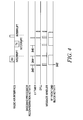
timer 314 generates a trigger signal attime 340 which triggers themessage handler 316 to provide a message associated with the DPLL desense operation to the baseband DPLLperipheral device 318 via therouter 315. The message includes an address associated with the baseband DPLLperipheral device 318 to enable therouter 315 to route the message to the baseband DPLLperipheral device 318 and operating parameters for the desense operation. On receipt of the message from therouter 315, the operating parameters in the received message is written to the configuration register associated with the baseband DPLLperipheral device 318 such that attime 340 the operation of the baseband DPLLperipheral device 318 is reconfigured or controlled according to the operating parameters in the received message. Attime 342, the layer onetimer 314 generates a further trigger signal (as set out in the macro table in thetimer 314 for the receive operation), which triggers themessage handler 316 to provide messages to the RFfront end block 306 in order to control the operation of the RF receive elements of the RFfront end block 306 for a receive operation. Attime 344, the layer onetimer 314 generates a trigger signal which triggers themessage handler 316 to provide a message associated with the DPLL desense operation to the baseband DPLLperipheral device 318 via therouter 315 as discussed above. TheMS 300 is thus arranged to perform a DPLL desense operation before and after a receive operation by means of the trigger signals generated by the layer onetimer 314. The layer onetimer 314 is also programmed to time the reconfiguration or programming of the RFfront end block 306 for a transmit operation and attime 346 generates a trigger signal which is transmitted to themessage handler 316 in order to control the operation of the RF transmit elements of the RFfront end block 306 for a transmit operation. - Referring now to
FIG. 5 , when an event requiring a change in the sampling rate is called, for example, when its is determined that the sampling rate can be 1x rather than 2x which helps to limit current drain in thebaseband block 310, the layer onetimer 314 generates a trigger signal attime 350 which triggers themessage handler 316 to provide a message associated with the dynamic sampling rate event to the baseband BPPperipheral device 318 via therouter 315. The message includes an address associated with the baseband BPPperipheral device 318 to enable therouter 315 to route the message to the baseband BPPperipheral device 318 and operating parameters to change the sampling rate to 1x. On receipt of the message from therouter 315, the operating parameters in the received message is written to the configuration register of the baseband BPPperipheral device 318 such that attime 350 the operation of the baseband BPPperipheral device 318 is reconfigured or controlled according to the operating parameters in the received message. Attime 352, the layer onetimer 314 generates a further trigger signal (as set out in the macro table in thetimer 314 for the dynamic sampling rate event), which triggers themessage handler 316 to provide a message associated with the dynamic sampling rate operation to the RFfront end block 306 in order to control the operation of the relevant part of the RFfront end block 306 for the x1 or x2 sampling rate.. - As can be seen from
FIGs. 4 and5 , the operation of the peripheral devices, the baseband DPLL peripheral device ofFIG. 4 and the baseband BPP peripheral device ofFIG. 5 , can be controlled by thetimer 314, themessage handler 316 and therouter 315 for an event, such as a desense event or dynamic sampling rate, without the need to interrupt theprocessor 312 for reconfiguration activity. Since the layer onetimer 314 generates the trigger signals which trigger themessage handler 316, the messages are time accurate. Moreover, since theprocessor 312 is not required to reconfigure the baseband DPLL peripheral device, the reconfiguration can occur more quickly and so in real-time. Thus, the arrangement in accordance with the disclosure can ensure fast enough reconfiguration to enable sampling rates to be switched. - It will be appreciated that the arrangement in accordance with the disclosure may also be used for reconfiguring or programming elements of the RF
front end block 306. In such an embodiment, therouter 315 would send messages fetched from themessage handler 316 to the RFfront end block 306 via interfaces such as SPI blocks. - The arrangement in accordance with the disclosure can provide similar advantages with other examples of events that require time accurate control of baseband peripheral devices including:
- a) Tuned antenna with multiple band dependencies which operation requires the antenna to be switched to different bands at appropriate times and requires the use of a baseband General Purpose Input/Output (GPIO) peripheral device in order to set up the appropriate operating conditions in the RF
front end block 306. The timing diagram for such an operation is similar to that ofFIG. 4 . In another embodiment, it can be arranged such that a GPIO is not used to set up the appropriate conditions in the RFfront end block 306 and instead the layer one timer is used wherein reconfiguration based on band information could be achieved by the layer one timer pins. - b) RF front end block with band dependencies.
- c) Clock speed gear shifting of message handler.
- d) RF activation boundary configuration (e.g. for BBP).
- e) Dynamic message handler queue allocation (for single receiver architecture).
- f) Reprogramming of the layer one timer in real-time.
- g) Switching active devices to a low power state for power management.
- Since the
router 315 in accordance with the disclosure routes messages from themessage handler 316 to the peripheral device associated with the message, existing buses can be used and there is no need to define new blocks to handle the different operating configurations. For example, different operating configurations can be achieved according to the content of the messages handled by themessage handler 316 and therouter 315 without the need for complex software solutions. Furthermore, since the messages from themessage handler 316 for the peripheral devices and the messages from theprocessor 312 to themessage handler 316 are routed through therouter 315, therouter 315 can handle contention and arbitration issues which exist between theprocessor 312 and themessage handler 316 when accessing the plurality of peripheral devices. - In summary, the present disclosure provides an arrangement for communicating messages between a processor and a plurality of peripheral devices which messages can control the operation of associated peripheral devices without the use of software interrupts and in a time accurate manner by way of a timer. The present disclosure enables any peripheral device including RF elements in the RF front end block to be reconfigured and so can help to solve many real-time issues.
Claims (9)
- A message handling arrangement for communicating messages between a processor and a plurality of peripheral devices in a communication device, each message including operation data for controlling the operation of a peripheral device for an event, the processing device comprising:a timer for generating trigger signals for triggering events;a message handler for receiving from the main processor at least one message associated with one of the plurality of peripheral devices and with an event and for transmitting the at least one message in response to a trigger signal generated by the timer for the event; anda router coupled to the message handler for receiving the at least one message transmitted by the message handler and for communicating the at least one message to the associated one of the plurality of peripheral devices.
- The message handling arrangement of claim 1, wherein each of the at least one message includes an address of the peripheral device associated with the at least one message, wherein the router is arranged to use the address in the message to communicate the message to the associated one of the peripheral devices.
- A processing arrangement for a communication device comprising a processor; a plurality of peripheral devices and the message handling arrangement as recited in any preceding claim for communicating messages between the processor and the plurality of peripheral devices, wherein in response to receiving a message, a peripheral device associated with the received message is arranged to control the operation of the peripheral device according to the operation data in the received message.
- The processing arrangement of claim 3, wherein the timer includes a layer 1 timer.
- The processing arrangement of claim 3, 4, 5 or 6, wherein the router is coupled to the processor and to the message handler, the router being arranged to communicate messages from the processor to the message handler and from the message handler to the plurality of peripheral devices.
- The processing arrangement of claim 3, 4 or 5, wherein the processor includes a baseband processor and the plurality of peripheral devices include a plurality of baseband peripheral devices.
- The processing arrangement of claim 6, wherein the plurality of baseband peripheral devices include at least one of a baseband DPLL peripheral device, a baseband General Purpose Input/Output device GPIO peripheral device, a baseband port BBP peripheral device and the timer.
- A communication device including an RF front end block for providing an RF receive path and an RF transmit path for the communication device and a baseband block coupled to the RF front end block, the baseband block including a processing arrangement as recited in claim 6 or 7.
- A method of communicating messages between a processor and a plurality of peripheral devices in a communication device, each message including operation data for controlling the operation of a peripheral device for an event, the method comprising the steps of:receiving at a message handler from the processor at least one message associated with one of the plurality of peripheral devices and with an event;generating by a timer a trigger signal for initiating the event;transmitting by the message handler the at least one message in response to the trigger signal generated by the timer;receiving by a router the at least one message transmitted by the message handler and for communicating the at least one message to the associated one of the plurality of peripheral devices; andcontrolling the operation of the associated one of the plurality of peripheral devices in response to the at least one message received by the associated one of the plurality of peripheral devices.
Priority Applications (2)
| Application Number | Priority Date | Filing Date | Title |
|---|---|---|---|
| EP07290727.2A EP2068250B1 (en) | 2007-06-08 | 2007-06-08 | Method and apparatuses for communicating a message received from a main processor to a peripheral device |
| PCT/US2008/065696 WO2008154232A1 (en) | 2007-06-08 | 2008-06-04 | Method and apparatus for communicating a message received from a mian processor to a peripheral device |
Applications Claiming Priority (1)
| Application Number | Priority Date | Filing Date | Title |
|---|---|---|---|
| EP07290727.2A EP2068250B1 (en) | 2007-06-08 | 2007-06-08 | Method and apparatuses for communicating a message received from a main processor to a peripheral device |
Publications (3)
| Publication Number | Publication Date |
|---|---|
| EP2068250A2 true EP2068250A2 (en) | 2009-06-10 |
| EP2068250A3 EP2068250A3 (en) | 2009-10-21 |
| EP2068250B1 EP2068250B1 (en) | 2016-02-17 |
Family
ID=38969428
Family Applications (1)
| Application Number | Title | Priority Date | Filing Date |
|---|---|---|---|
| EP07290727.2A Active EP2068250B1 (en) | 2007-06-08 | 2007-06-08 | Method and apparatuses for communicating a message received from a main processor to a peripheral device |
Country Status (2)
| Country | Link |
|---|---|
| EP (1) | EP2068250B1 (en) |
| WO (1) | WO2008154232A1 (en) |
Families Citing this family (1)
| Publication number | Priority date | Publication date | Assignee | Title |
|---|---|---|---|---|
| FR3004038B1 (en) | 2013-03-27 | 2016-11-11 | Thales Sa | INTERFACE ARCHITECTURE BETWEEN DIGITAL AND RADIO UNITS. |
Citations (3)
| Publication number | Priority date | Publication date | Assignee | Title |
|---|---|---|---|---|
| US20050265507A1 (en) * | 2003-12-29 | 2005-12-01 | Charbel Khawand | Method and system for employing adaptive event codes |
| US20060010264A1 (en) * | 2000-06-09 | 2006-01-12 | Rader Sheila M | Integrated processor platform supporting wireless handheld multi-media devices |
| WO2006027026A1 (en) * | 2004-09-07 | 2006-03-16 | Freescale Semiconductors, Inc | Apparatus and control interface therefor |
-
2007
- 2007-06-08 EP EP07290727.2A patent/EP2068250B1/en active Active
-
2008
- 2008-06-04 WO PCT/US2008/065696 patent/WO2008154232A1/en active Application Filing
Patent Citations (3)
| Publication number | Priority date | Publication date | Assignee | Title |
|---|---|---|---|---|
| US20060010264A1 (en) * | 2000-06-09 | 2006-01-12 | Rader Sheila M | Integrated processor platform supporting wireless handheld multi-media devices |
| US20050265507A1 (en) * | 2003-12-29 | 2005-12-01 | Charbel Khawand | Method and system for employing adaptive event codes |
| WO2006027026A1 (en) * | 2004-09-07 | 2006-03-16 | Freescale Semiconductors, Inc | Apparatus and control interface therefor |
Non-Patent Citations (1)
| Title |
|---|
| FLIK T: "Mikroprozessortechnik - 8 - EIN-/AUSGABESTEUEREINHEITEN, PERIPHERIEBUSSE UND HINTERGRUNDSPEICHER" MIKROPROZESSORTECHNIK, XX, XX, 2001, pages 516-529, XP002383180 * |
Also Published As
| Publication number | Publication date |
|---|---|
| WO2008154232A1 (en) | 2008-12-18 |
| EP2068250B1 (en) | 2016-02-17 |
| EP2068250A3 (en) | 2009-10-21 |
Similar Documents
| Publication | Publication Date | Title |
|---|---|---|
| JP5002783B2 (en) | Communication device including dual timer unit | |
| US11800513B2 (en) | Method of information transmission in unlicensed band, terminal, and network device | |
| US6125404A (en) | Data processing system having a protocol timer for autonomously providing time based interrupts | |
| US7013398B2 (en) | Data processor architecture employing segregated data, program and control buses | |
| GB2357401A (en) | Updating a timing offset in a communications device | |
| CN101263660B (en) | Signal processing task scheduling in a communication apparatus | |
| US20080293445A1 (en) | Radio frequency apparatus | |
| US20050228913A1 (en) | Communication apparatus implementing time domain isolation with restricted bus access | |
| US20080242347A1 (en) | Fast multiradio context switching | |
| JP5985711B2 (en) | Apparatus, system and method for parallelizing UE wake-up process | |
| US20190335538A1 (en) | Enhanced wci-2 message for coexistence management | |
| TWI407743B (en) | Method and system for sharing components in a time division multiplex wireless system | |
| US7283503B1 (en) | Communication apparatus including a buffer circuit having first and second portions for alternately storing results | |
| EP2068250B1 (en) | Method and apparatuses for communicating a message received from a main processor to a peripheral device | |
| US11106612B2 (en) | Coordinating operations of multiple communication chips via local hub device | |
| EP1877890B1 (en) | Communication apparatus having a sim interface compatible with radio isolation | |
| US10733117B2 (en) | Programmable radio transceivers | |
| WO2008023356A2 (en) | Sdr based method of multi-mode radio timing scheduling | |
| CN105828423B (en) | For controlling the devices, systems, and methods of the decoded adaptive sleep scheduling of signal | |
| JP4612205B2 (en) | Control unit for communication system terminal, cordless telecommunications system terminal including the control unit, and control method therefor |
Legal Events
| Date | Code | Title | Description |
|---|---|---|---|
| PUAI | Public reference made under article 153(3) epc to a published international application that has entered the european phase |
Free format text: ORIGINAL CODE: 0009012 |
|
| PUAI | Public reference made under article 153(3) epc to a published international application that has entered the european phase |
Free format text: ORIGINAL CODE: 0009012 |
|
| AK | Designated contracting states |
Kind code of ref document: A2 Designated state(s): AT BE BG CH CY CZ DE DK EE ES FI FR GB GR HU IE IS IT LI LT LU LV MC MT NL PL PT RO SE SI SK TR |
|
| AX | Request for extension of the european patent |
Extension state: AL BA HR MK RS |
|
| 17P | Request for examination filed |
Effective date: 20090504 |
|
| PUAL | Search report despatched |
Free format text: ORIGINAL CODE: 0009013 |
|
| AK | Designated contracting states |
Kind code of ref document: A3 Designated state(s): AT BE BG CH CY CZ DE DK EE ES FI FR GB GR HU IE IS IT LI LT LU LV MC MT NL PL PT RO SE SI SK TR |
|
| AX | Request for extension of the european patent |
Extension state: AL BA HR MK RS |
|
| AKX | Designation fees paid |
Designated state(s): AT BE BG CH CY CZ DE DK EE ES FI FR GB GR HU IE IS IT LI LT LU LV MC MT NL PL PT RO SE SI SK TR |
|
| RAP1 | Party data changed (applicant data changed or rights of an application transferred) |
Owner name: MOTOROLA MOBILITY, INC. |
|
| RAP1 | Party data changed (applicant data changed or rights of an application transferred) |
Owner name: MOTOROLA MOBILITY LLC |
|
| REG | Reference to a national code |
Ref country code: DE Ref legal event code: R079 Ref document number: 602007044855 Country of ref document: DE Free format text: PREVIOUS MAIN CLASS: G06F0015780000 Ipc: G06F0013240000 |
|
| GRAP | Despatch of communication of intention to grant a patent |
Free format text: ORIGINAL CODE: EPIDOSNIGR1 |
|
| RIC1 | Information provided on ipc code assigned before grant |
Ipc: G06F 13/24 20060101AFI20150716BHEP |
|
| INTG | Intention to grant announced |
Effective date: 20150805 |
|
| GRAS | Grant fee paid |
Free format text: ORIGINAL CODE: EPIDOSNIGR3 |
|
| GRAA | (expected) grant |
Free format text: ORIGINAL CODE: 0009210 |
|
| AK | Designated contracting states |
Kind code of ref document: B1 Designated state(s): AT BE BG CH CY CZ DE DK EE ES FI FR GB GR HU IE IS IT LI LT LU LV MC MT NL PL PT RO SE SI SK TR |
|
| REG | Reference to a national code |
Ref country code: GB Ref legal event code: FG4D |
|
| REG | Reference to a national code |
Ref country code: CH Ref legal event code: EP |
|
| REG | Reference to a national code |
Ref country code: IE Ref legal event code: FG4D |
|
| REG | Reference to a national code |
Ref country code: AT Ref legal event code: REF Ref document number: 775942 Country of ref document: AT Kind code of ref document: T Effective date: 20160315 |
|
| REG | Reference to a national code |
Ref country code: DE Ref legal event code: R096 Ref document number: 602007044855 Country of ref document: DE |
|
| RAP2 | Party data changed (patent owner data changed or rights of a patent transferred) |
Owner name: GOOGLE TECHNOLOGY HOLDINGS LLC |
|
| REG | Reference to a national code |
Ref country code: NL Ref legal event code: MP Effective date: 20160217 |
|
| REG | Reference to a national code |
Ref country code: LT Ref legal event code: MG4D |
|
| REG | Reference to a national code |
Ref country code: FR Ref legal event code: PLFP Year of fee payment: 10 |
|
| REG | Reference to a national code |
Ref country code: AT Ref legal event code: MK05 Ref document number: 775942 Country of ref document: AT Kind code of ref document: T Effective date: 20160217 |
|
| PG25 | Lapsed in a contracting state [announced via postgrant information from national office to epo] |
Ref country code: IT Free format text: LAPSE BECAUSE OF FAILURE TO SUBMIT A TRANSLATION OF THE DESCRIPTION OR TO PAY THE FEE WITHIN THE PRESCRIBED TIME-LIMIT Effective date: 20160217 Ref country code: GR Free format text: LAPSE BECAUSE OF FAILURE TO SUBMIT A TRANSLATION OF THE DESCRIPTION OR TO PAY THE FEE WITHIN THE PRESCRIBED TIME-LIMIT Effective date: 20160518 Ref country code: FI Free format text: LAPSE BECAUSE OF FAILURE TO SUBMIT A TRANSLATION OF THE DESCRIPTION OR TO PAY THE FEE WITHIN THE PRESCRIBED TIME-LIMIT Effective date: 20160217 Ref country code: ES Free format text: LAPSE BECAUSE OF FAILURE TO SUBMIT A TRANSLATION OF THE DESCRIPTION OR TO PAY THE FEE WITHIN THE PRESCRIBED TIME-LIMIT Effective date: 20160217 |
|
| PG25 | Lapsed in a contracting state [announced via postgrant information from national office to epo] |
Ref country code: LT Free format text: LAPSE BECAUSE OF FAILURE TO SUBMIT A TRANSLATION OF THE DESCRIPTION OR TO PAY THE FEE WITHIN THE PRESCRIBED TIME-LIMIT Effective date: 20160217 Ref country code: PT Free format text: LAPSE BECAUSE OF FAILURE TO SUBMIT A TRANSLATION OF THE DESCRIPTION OR TO PAY THE FEE WITHIN THE PRESCRIBED TIME-LIMIT Effective date: 20160617 Ref country code: PL Free format text: LAPSE BECAUSE OF FAILURE TO SUBMIT A TRANSLATION OF THE DESCRIPTION OR TO PAY THE FEE WITHIN THE PRESCRIBED TIME-LIMIT Effective date: 20160217 Ref country code: SE Free format text: LAPSE BECAUSE OF FAILURE TO SUBMIT A TRANSLATION OF THE DESCRIPTION OR TO PAY THE FEE WITHIN THE PRESCRIBED TIME-LIMIT Effective date: 20160217 Ref country code: AT Free format text: LAPSE BECAUSE OF FAILURE TO SUBMIT A TRANSLATION OF THE DESCRIPTION OR TO PAY THE FEE WITHIN THE PRESCRIBED TIME-LIMIT Effective date: 20160217 Ref country code: LV Free format text: LAPSE BECAUSE OF FAILURE TO SUBMIT A TRANSLATION OF THE DESCRIPTION OR TO PAY THE FEE WITHIN THE PRESCRIBED TIME-LIMIT Effective date: 20160217 Ref country code: NL Free format text: LAPSE BECAUSE OF FAILURE TO SUBMIT A TRANSLATION OF THE DESCRIPTION OR TO PAY THE FEE WITHIN THE PRESCRIBED TIME-LIMIT Effective date: 20160217 |
|
| PG25 | Lapsed in a contracting state [announced via postgrant information from national office to epo] |
Ref country code: EE Free format text: LAPSE BECAUSE OF FAILURE TO SUBMIT A TRANSLATION OF THE DESCRIPTION OR TO PAY THE FEE WITHIN THE PRESCRIBED TIME-LIMIT Effective date: 20160217 Ref country code: DK Free format text: LAPSE BECAUSE OF FAILURE TO SUBMIT A TRANSLATION OF THE DESCRIPTION OR TO PAY THE FEE WITHIN THE PRESCRIBED TIME-LIMIT Effective date: 20160217 |
|
| REG | Reference to a national code |
Ref country code: DE Ref legal event code: R097 Ref document number: 602007044855 Country of ref document: DE |
|
| PG25 | Lapsed in a contracting state [announced via postgrant information from national office to epo] |
Ref country code: RO Free format text: LAPSE BECAUSE OF FAILURE TO SUBMIT A TRANSLATION OF THE DESCRIPTION OR TO PAY THE FEE WITHIN THE PRESCRIBED TIME-LIMIT Effective date: 20160217 Ref country code: SK Free format text: LAPSE BECAUSE OF FAILURE TO SUBMIT A TRANSLATION OF THE DESCRIPTION OR TO PAY THE FEE WITHIN THE PRESCRIBED TIME-LIMIT Effective date: 20160217 Ref country code: CZ Free format text: LAPSE BECAUSE OF FAILURE TO SUBMIT A TRANSLATION OF THE DESCRIPTION OR TO PAY THE FEE WITHIN THE PRESCRIBED TIME-LIMIT Effective date: 20160217 |
|
| PLBE | No opposition filed within time limit |
Free format text: ORIGINAL CODE: 0009261 |
|
| STAA | Information on the status of an ep patent application or granted ep patent |
Free format text: STATUS: NO OPPOSITION FILED WITHIN TIME LIMIT |
|
| PG25 | Lapsed in a contracting state [announced via postgrant information from national office to epo] |
Ref country code: BE Free format text: LAPSE BECAUSE OF FAILURE TO SUBMIT A TRANSLATION OF THE DESCRIPTION OR TO PAY THE FEE WITHIN THE PRESCRIBED TIME-LIMIT Effective date: 20160217 |
|
| 26N | No opposition filed |
Effective date: 20161118 |
|
| PG25 | Lapsed in a contracting state [announced via postgrant information from national office to epo] |
Ref country code: MC Free format text: LAPSE BECAUSE OF FAILURE TO SUBMIT A TRANSLATION OF THE DESCRIPTION OR TO PAY THE FEE WITHIN THE PRESCRIBED TIME-LIMIT Effective date: 20160217 |
|
| REG | Reference to a national code |
Ref country code: CH Ref legal event code: PL |
|
| PG25 | Lapsed in a contracting state [announced via postgrant information from national office to epo] |
Ref country code: BG Free format text: LAPSE BECAUSE OF FAILURE TO SUBMIT A TRANSLATION OF THE DESCRIPTION OR TO PAY THE FEE WITHIN THE PRESCRIBED TIME-LIMIT Effective date: 20160517 Ref country code: SI Free format text: LAPSE BECAUSE OF FAILURE TO SUBMIT A TRANSLATION OF THE DESCRIPTION OR TO PAY THE FEE WITHIN THE PRESCRIBED TIME-LIMIT Effective date: 20160217 |
|
| REG | Reference to a national code |
Ref country code: IE Ref legal event code: MM4A |
|
| PG25 | Lapsed in a contracting state [announced via postgrant information from national office to epo] |
Ref country code: CH Free format text: LAPSE BECAUSE OF NON-PAYMENT OF DUE FEES Effective date: 20160630 Ref country code: LI Free format text: LAPSE BECAUSE OF NON-PAYMENT OF DUE FEES Effective date: 20160630 |
|
| PG25 | Lapsed in a contracting state [announced via postgrant information from national office to epo] |
Ref country code: IE Free format text: LAPSE BECAUSE OF NON-PAYMENT OF DUE FEES Effective date: 20160608 |
|
| REG | Reference to a national code |
Ref country code: FR Ref legal event code: PLFP Year of fee payment: 11 |
|
| REG | Reference to a national code |
Ref country code: DE Ref legal event code: R082 Ref document number: 602007044855 Country of ref document: DE Representative=s name: BETTEN & RESCH PATENT- UND RECHTSANWAELTE PART, DE Ref country code: DE Ref legal event code: R081 Ref document number: 602007044855 Country of ref document: DE Owner name: GOOGLE TECHNOLOGY HOLDINGS LLC, MOUNTAIN VIEW, US Free format text: FORMER OWNER: MOTOROLA MOBILITY LLC, LIBERTYVILLE, ILL., US |
|
| PG25 | Lapsed in a contracting state [announced via postgrant information from national office to epo] |
Ref country code: HU Free format text: LAPSE BECAUSE OF FAILURE TO SUBMIT A TRANSLATION OF THE DESCRIPTION OR TO PAY THE FEE WITHIN THE PRESCRIBED TIME-LIMIT; INVALID AB INITIO Effective date: 20070608 Ref country code: CY Free format text: LAPSE BECAUSE OF FAILURE TO SUBMIT A TRANSLATION OF THE DESCRIPTION OR TO PAY THE FEE WITHIN THE PRESCRIBED TIME-LIMIT Effective date: 20160217 |
|
| REG | Reference to a national code |
Ref country code: FR Ref legal event code: PLFP Year of fee payment: 12 |
|
| PG25 | Lapsed in a contracting state [announced via postgrant information from national office to epo] |
Ref country code: MT Free format text: LAPSE BECAUSE OF NON-PAYMENT OF DUE FEES Effective date: 20160630 Ref country code: TR Free format text: LAPSE BECAUSE OF FAILURE TO SUBMIT A TRANSLATION OF THE DESCRIPTION OR TO PAY THE FEE WITHIN THE PRESCRIBED TIME-LIMIT Effective date: 20160217 Ref country code: LU Free format text: LAPSE BECAUSE OF NON-PAYMENT OF DUE FEES Effective date: 20160608 Ref country code: IS Free format text: LAPSE BECAUSE OF FAILURE TO SUBMIT A TRANSLATION OF THE DESCRIPTION OR TO PAY THE FEE WITHIN THE PRESCRIBED TIME-LIMIT Effective date: 20160217 |
|
| PGFP | Annual fee paid to national office [announced via postgrant information from national office to epo] |
Ref country code: FR Payment date: 20190625 Year of fee payment: 13 |
|
| PG25 | Lapsed in a contracting state [announced via postgrant information from national office to epo] |
Ref country code: FR Free format text: LAPSE BECAUSE OF NON-PAYMENT OF DUE FEES Effective date: 20200630 |
|
| PGFP | Annual fee paid to national office [announced via postgrant information from national office to epo] |
Ref country code: DE Payment date: 20230626 Year of fee payment: 17 |
|
| PGFP | Annual fee paid to national office [announced via postgrant information from national office to epo] |
Ref country code: GB Payment date: 20230627 Year of fee payment: 17 |