EP2079111A1 - Nanoscale CMOS transister with an intrinsic bulk - Google Patents
Nanoscale CMOS transister with an intrinsic bulk Download PDFInfo
- Publication number
- EP2079111A1 EP2079111A1 EP08100315A EP08100315A EP2079111A1 EP 2079111 A1 EP2079111 A1 EP 2079111A1 EP 08100315 A EP08100315 A EP 08100315A EP 08100315 A EP08100315 A EP 08100315A EP 2079111 A1 EP2079111 A1 EP 2079111A1
- Authority
- EP
- European Patent Office
- Prior art keywords
- source
- region
- mosfet
- gate
- drain
- Prior art date
- Legal status (The legal status is an assumption and is not a legal conclusion. Google has not performed a legal analysis and makes no representation as to the accuracy of the status listed.)
- Withdrawn
Links
- 239000002019 doping agent Substances 0.000 claims abstract description 11
- 239000013590 bulk material Substances 0.000 claims abstract description 6
- 239000004065 semiconductor Substances 0.000 claims description 7
- XUIMIQQOPSSXEZ-UHFFFAOYSA-N Silicon Chemical compound [Si] XUIMIQQOPSSXEZ-UHFFFAOYSA-N 0.000 claims description 4
- 229910052710 silicon Inorganic materials 0.000 claims description 4
- 239000010703 silicon Substances 0.000 claims description 4
- 238000005036 potential barrier Methods 0.000 abstract description 11
- 230000004048 modification Effects 0.000 abstract 1
- 238000012986 modification Methods 0.000 abstract 1
- 230000000694 effects Effects 0.000 description 12
- 239000000969 carrier Substances 0.000 description 6
- 239000012535 impurity Substances 0.000 description 6
- 238000000034 method Methods 0.000 description 6
- 230000004888 barrier function Effects 0.000 description 5
- 230000007423 decrease Effects 0.000 description 3
- 125000001475 halogen functional group Chemical group 0.000 description 3
- 238000004519 manufacturing process Methods 0.000 description 2
- 238000004088 simulation Methods 0.000 description 2
- 210000000746 body region Anatomy 0.000 description 1
- 230000015556 catabolic process Effects 0.000 description 1
- 230000000295 complement effect Effects 0.000 description 1
- 230000003247 decreasing effect Effects 0.000 description 1
- 238000006731 degradation reaction Methods 0.000 description 1
- 230000001419 dependent effect Effects 0.000 description 1
- 238000009792 diffusion process Methods 0.000 description 1
- 238000009826 distribution Methods 0.000 description 1
- 239000012212 insulator Substances 0.000 description 1
- 238000005468 ion implantation Methods 0.000 description 1
- 230000003071 parasitic effect Effects 0.000 description 1
- 125000006850 spacer group Chemical group 0.000 description 1
- 239000000758 substrate Substances 0.000 description 1
- 230000001629 suppression Effects 0.000 description 1
Images


Classifications
-
- H—ELECTRICITY
- H01—ELECTRIC ELEMENTS
- H01L—SEMICONDUCTOR DEVICES NOT COVERED BY CLASS H10
- H01L29/00—Semiconductor devices adapted for rectifying, amplifying, oscillating or switching, or capacitors or resistors with at least one potential-jump barrier or surface barrier, e.g. PN junction depletion layer or carrier concentration layer; Details of semiconductor bodies or of electrodes thereof ; Multistep manufacturing processes therefor
- H01L29/02—Semiconductor bodies ; Multistep manufacturing processes therefor
- H01L29/06—Semiconductor bodies ; Multistep manufacturing processes therefor characterised by their shape; characterised by the shapes, relative sizes, or dispositions of the semiconductor regions ; characterised by the concentration or distribution of impurities within semiconductor regions
- H01L29/08—Semiconductor bodies ; Multistep manufacturing processes therefor characterised by their shape; characterised by the shapes, relative sizes, or dispositions of the semiconductor regions ; characterised by the concentration or distribution of impurities within semiconductor regions with semiconductor regions connected to an electrode carrying current to be rectified, amplified or switched and such electrode being part of a semiconductor device which comprises three or more electrodes
- H01L29/0843—Source or drain regions of field-effect devices
- H01L29/0847—Source or drain regions of field-effect devices of field-effect transistors with insulated gate
-
- H—ELECTRICITY
- H01—ELECTRIC ELEMENTS
- H01L—SEMICONDUCTOR DEVICES NOT COVERED BY CLASS H10
- H01L29/00—Semiconductor devices adapted for rectifying, amplifying, oscillating or switching, or capacitors or resistors with at least one potential-jump barrier or surface barrier, e.g. PN junction depletion layer or carrier concentration layer; Details of semiconductor bodies or of electrodes thereof ; Multistep manufacturing processes therefor
- H01L29/02—Semiconductor bodies ; Multistep manufacturing processes therefor
- H01L29/06—Semiconductor bodies ; Multistep manufacturing processes therefor characterised by their shape; characterised by the shapes, relative sizes, or dispositions of the semiconductor regions ; characterised by the concentration or distribution of impurities within semiconductor regions
- H01L29/10—Semiconductor bodies ; Multistep manufacturing processes therefor characterised by their shape; characterised by the shapes, relative sizes, or dispositions of the semiconductor regions ; characterised by the concentration or distribution of impurities within semiconductor regions with semiconductor regions connected to an electrode not carrying current to be rectified, amplified or switched and such electrode being part of a semiconductor device which comprises three or more electrodes
- H01L29/107—Substrate region of field-effect devices
- H01L29/1075—Substrate region of field-effect devices of field-effect transistors
- H01L29/1079—Substrate region of field-effect devices of field-effect transistors with insulated gate
-
- H—ELECTRICITY
- H01—ELECTRIC ELEMENTS
- H01L—SEMICONDUCTOR DEVICES NOT COVERED BY CLASS H10
- H01L29/00—Semiconductor devices adapted for rectifying, amplifying, oscillating or switching, or capacitors or resistors with at least one potential-jump barrier or surface barrier, e.g. PN junction depletion layer or carrier concentration layer; Details of semiconductor bodies or of electrodes thereof ; Multistep manufacturing processes therefor
- H01L29/40—Electrodes ; Multistep manufacturing processes therefor
- H01L29/41—Electrodes ; Multistep manufacturing processes therefor characterised by their shape, relative sizes or dispositions
- H01L29/417—Electrodes ; Multistep manufacturing processes therefor characterised by their shape, relative sizes or dispositions carrying the current to be rectified, amplified or switched
- H01L29/41725—Source or drain electrodes for field effect devices
- H01L29/41758—Source or drain electrodes for field effect devices for lateral devices with structured layout for source or drain region, i.e. the source or drain region having cellular, interdigitated or ring structure or being curved or angular
-
- H—ELECTRICITY
- H01—ELECTRIC ELEMENTS
- H01L—SEMICONDUCTOR DEVICES NOT COVERED BY CLASS H10
- H01L29/00—Semiconductor devices adapted for rectifying, amplifying, oscillating or switching, or capacitors or resistors with at least one potential-jump barrier or surface barrier, e.g. PN junction depletion layer or carrier concentration layer; Details of semiconductor bodies or of electrodes thereof ; Multistep manufacturing processes therefor
- H01L29/40—Electrodes ; Multistep manufacturing processes therefor
- H01L29/41—Electrodes ; Multistep manufacturing processes therefor characterised by their shape, relative sizes or dispositions
- H01L29/417—Electrodes ; Multistep manufacturing processes therefor characterised by their shape, relative sizes or dispositions carrying the current to be rectified, amplified or switched
- H01L29/41725—Source or drain electrodes for field effect devices
- H01L29/41766—Source or drain electrodes for field effect devices with at least part of the source or drain electrode having contact below the semiconductor surface, e.g. the source or drain electrode formed at least partially in a groove or with inclusions of conductor inside the semiconductor
-
- H—ELECTRICITY
- H01—ELECTRIC ELEMENTS
- H01L—SEMICONDUCTOR DEVICES NOT COVERED BY CLASS H10
- H01L29/00—Semiconductor devices adapted for rectifying, amplifying, oscillating or switching, or capacitors or resistors with at least one potential-jump barrier or surface barrier, e.g. PN junction depletion layer or carrier concentration layer; Details of semiconductor bodies or of electrodes thereof ; Multistep manufacturing processes therefor
- H01L29/66—Types of semiconductor device ; Multistep manufacturing processes therefor
- H01L29/68—Types of semiconductor device ; Multistep manufacturing processes therefor controllable by only the electric current supplied, or only the electric potential applied, to an electrode which does not carry the current to be rectified, amplified or switched
- H01L29/76—Unipolar devices, e.g. field effect transistors
- H01L29/772—Field effect transistors
- H01L29/78—Field effect transistors with field effect produced by an insulated gate
Definitions
- the present invention relates to nanoscale MOSFETs. More particularly, the present invention relates to nano size MOSFET smaller than 80nm and down to 10nm, without the need to dope the channel region.
- MOSFETs scaling results in problems due to the short distance between the source and the drain. Such problems, which include Drain Induced Barrier Lowering (DIBL) and punch through result in large leakage current and have hampered the possibility of scaling the gate length of MOSFETs below 80 nm.
- DIBL Drain Induced Barrier Lowering
- CMOS complementary MOS circuits
- parasitic thyristors which are created by these well dopings create latch up problems.
- extra steps have been introduced in fabrication process. These steps add yet to the cost and also consume wafer space.
- the US patent document US 5489792 describes a silicon on insulator (SOI) MOSFET transistor in which the source is doped by two opposite regions; the bottom region is lightly doped with respect to the top region and the channel is doped.
- SOI silicon on insulator
- the function of the oppositely doped region is to create a contact to the floating body of the SOI structure in order to collect carriers which are created by impact ionization.
- the collection of impact ionization carriers is only relevant to SOI structures for which a floating body might exist; it yet loses any meaning for MOSFET using bulk substrates.
- the invention discloses a new MOSFET transistor aimed at reducing problems with dopant fluctuations, CMOS latch up, and short channel effects, such as DIBL and punch through.
- a goal of the present invention is to propose a new MOSFET fabricated on intrinsic bulk material, so that the dopant fluctuation is eliminated, n and p devices are fabricated without the need to introduce "well” regions, and the mobility of carriers is increased due to an intrinsic channel region, and the regular thyristor latch up problems in CMOS circuits are eliminated.
- the very large Ion/loff ratio as well as the on and off state currents for both n and p type devices indicate that short channel effects are greatly suppressed as well.
- the nanoscale MOSFET according to the invention allows to overcome the problems of scalability of the gate length below 50 nm and down to 10nm due to short channel effects and doping profile fluctuations. It further does not need a doped channel region to operate properly.
- the present invention also provides methods to fabricate the said region inside the source and the drain. They can be fabricated either by epitaxial growth or by placing the two oppositely doped regions side by side along the width of the source.
- the subject of this invention has been simulated using PISCESS-IIb program which is suitable for overall device lengths down to about 50 nm. Simulations also show that the short channel effects which are encountered in regular MOSFET devices are greatly reduced, without the need to use retrograde or halo doped regions. As simulations show, when the gate voltage is zero the device does turn off and very low leakage current is obtained.
- the source comprises of two regions of opposite dopant types.
- the idea of using an intrinsic bulk material in nano dimensions is counter intuitive because in regular MOSFETs the bulk material must be highly doped to reduce short channel effects and yet a MOSFET with an intrinsic bulk does not operate as a transistor and does not turn off. Having a device which has an intrinsic bulk, with well defined on and off states, without suffering from short channel effects must operate based on unforeseen effects.
- the oppositely doped bottom region of the source creates such effects. It essentially pins the source/ body potential barrier, and this barrier becomes essentially voltage independent, as the voltage of the drain is increased. This is why the problems due to DIBL and punch through are effectively reduced or eliminated. It is thus possible for the gate to decrease or increase this barrier, as a result, the device can be turned on and off.
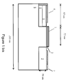
- a cross-sectional view is shown of an illustrative embodiment of the present invention for dimensions most relevant in today's electronic circuitry.
- the gate 1 is disposed over the oxide layer 2 which is disposed on the active body of the semiconductor 8.
- the source comprises two regions 3 and 4 of opposite dopings.
- the region 3 serves two purposes: it makes it possible for the gate voltage to modulate the current from source to the drain by introducing a potential barrier between region 4 and the channel, which can be lowered or increased by the gate; and it also greatly reduces the DIBL problem.
- DIBL refers to the fact that when the drain is too close to the source such that a voltage applied to it can affect the source side, the potential barrier between the source and body decreases.
- DIBL causes problems both in the on and off state of the transistor.
- DIBL causes the current to become dependent on the drain voltage which is not desired.
- DIBL causes leakage current as the carriers of the source can go over the lowered potential barrier.
- Region 3 provides therefore better "ON" characteristics with respect to regular MOSFETs, and it also provides much better lon/loff ratio.
- Regions 5, 6 and 7 are respectively the drain, and connections to the source and the drain, respectively.
- the extra dopant region 3 cannot, and should not, be considered as a halo region or lightly doped region as in LDD (lightly doped drain) transistors, since it is not only doped, but preferably highly doped on the source side, with the opposite doping type. Furthermore, this extra dopant region is electrically connected to the source itself. The DIBL lowering and punch-through limitation derived from this feature would not be possible otherwise.
- the source region comprises a lower portion 3 of a first doping type, and an upper portion 4 of a second doping type proximate to the silicon layer surface of the gate 1.
- the upper portion 4 extends from the edge to the gate 1 so that it covers the lower portion 3 only partially, and contact 6 is made to both portions.
- the upper and lower layers are in this example preferably made through ion implantation.
- FIG. 1 bis illustrates another embodiment of the invention in which epitaxial growth can be used for the source and the drain 5 as proposed in prior art.
- US 6,946,371, Sept 20, 2005 Langdo, et al "Methods of fabricating semiconductor structures having epitaxially grown source and drain elements" can be used or other relevant methods disclosed in the art.
- the region 3 covers entirely the region 4 as a superimposed layer.
- the connector 6 has therefore a different shape as in Figure 1 .
- the feature which is different from regular MOSFETs for all possible embodiments is the particular doping of the source.
- Another feature of the MOSFET according to the invention is to have an intrinsic bulk semiconductor in which p and n channel MOSFETs are fabricated on the same intrinsic bulk material without n and p well regions.
- the PISCES-IIb semiconductor drift-diffusion simulator has been used to obtain the characteristics of the disclosed invention.
- the potential and current voltage characteristics of our invention have been obtained with the dimensions indicated on FIG. 1 , that is the drain 5 and source 3 size (85nm), gate 1 length (75nm), drain 5 and source 3/4 thickness (50nm), wherein the source region 4 is of 40 nm width and 25nm thickness, body region 8 thickness (250 micrometer).
- the overall device width is 245nm.
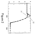
- FIG. 2 compares the potential barrier from the source to the drain for our invention (arrow 22) and a regular MOSFET (arrow 21) of the same gate length and a bulk with a doping density of 10 17 /cm3.
- This MOSFET does not have halo doping and it suffers from short channels effects; the figure is provided to demonstrate the ability of the disclosed invention to reduce short channel effects.
- the gate length is indicated in nanometers on the X axis and the potential is indicated in volts on the Y axis.
- the potential barrier for present invention has not been lowered by the drain voltage, while the regular MOSFET shows the barrier lowering as a result of the drain voltage. This is a clear indication that the problem of has been reduced by this invention.
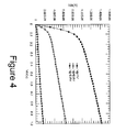
- FIG.3 and FIG.4 show the current I ds between the drain and the source as a function of the voltage V ds between the drain and the source, for different gate voltages Vg, for a regular MOSFET and the MOSFET according to the invention respectively. Comparing Fig3 with Fig4 , it can be observed that the magnitude of the ON current for the regular MOSFET and the subject of this invention are comparable. However, it can be appreciated that the less steep slope of the current-voltage relation, as well as the current magnitude with respect to the gate voltage, indicate that the short channel effects are much less severe for the subject of this invention, which has an intrinsic bulk.
- FIG. 5 and FIG.6 compare the OFF currents I ds of a regular MOSFET and the proposed MOSFET according to this invention, i.e. when the gate voltage Vg is equal to zero, as a function of the drain-source voltage V ds .
- the OFF current of the present invention is orders of magnitude less than the one for a regular MOSFET.
- the device according to the invention is intrinsic and has much less OFF current than a MOSFET doped by 10 17 / cm3 impurities.
- a p-type device By switching the impurity types of the source and drain, a p-type device is obtained and its OFF current is exactly what is shown on Fig.6 .
- P and n-channel devices can thus be obtained using an intrinsic bulk with a very small turn off current, whereby the drastically reduced leakage current in OFF state materializes the suppression of short effect channels.
- FIG. 6 and FIG. 7 illustrate the intensity-voltage (I-V) relation for a p channel device according to the disclosed invention.
- the device is similar to the n channel device with an intrinsic bulk, but the source and drain doping impurities are reversed.
- region 3 is n-doped with 10 18 / cm3 impurity concentration and regions 4 and 5 are p-doped with 10 19 / cm3 impurity concentration.
- ON and OFF states there are well defined ON and OFF states. A regular MOSFET would not turn off, if its bulk was intrinsic.
Abstract

Description
- The present invention relates to nanoscale MOSFETs. More particularly, the present invention relates to nano size MOSFET smaller than 80nm and down to 10nm, without the need to dope the channel region.
-
-
- 1- H.-S. P. Wong, D. J. Frank, P. M. Solomon, C. H.-J. Wann, and J. J. Welser, "Nanoscale CMOS," Proc. IEEE, vol. 87, no. 4, pp. 537-570, 1999.
- 2- T. Mizuno, "New channel engineering for sub-100 nm MOS devices considering both carrier velocity overshoot and statistical performance fluctuations," IEEE Trans. Elec. Dev. vol. 47, no. 4, pp. 756-761, 2000.
- 5- E. Murakami, T. Yoshimura, Y. Goto, S. Kimura, "Gate length scalability of n-MOSFETs down to 30 nm: Comparison between LDD and non-LDD structures," IEEE Trans. Electron Dev. vol. 47, no. 4, pp. 835-840, 2000.
- 6- D. S. Ang, C. H. Ling, "A reassessment of ac hot-carrier degradation in deep-submicrometer LDD N-MOSFET," IEEE Electron Dev. Lett., vol. 24, no. 9, pp. 598-600, 2003.
- Koh et al., "Body-Contacted SOI MOSFET Structure with Fully Bulk CMOS Compatible Layout and Process", IEEE Electron Device Letters, vol. 18, No. 3, Mar. 1997, pp. 102-104.
- The semiconductor industry has progressed in continuously decreasing the size of MOSFET transistors, in a process which is referred to as scaling. MOSFETs scaling results in problems due to the short distance between the source and the drain. Such problems, which include Drain Induced Barrier Lowering (DIBL) and punch through result in large leakage current and have hampered the possibility of scaling the gate length of MOSFETs below 80 nm.
- Another foreseen problem which occurs when device lengths are scaled down to about 10 nm, is the random nature of dopant distribution, dopant density fluctuations, in the channel region, which can cause undesirable threshold voltage variation across the wafer.
- In conventional complementary MOS circuits (CMOS) in which both n and p channel devices are fabricated in close proximity of each other, there is a need to create deep n and p type regions called wells. The parasitic thyristors which are created by these well dopings create latch up problems. To alleviate such problems, extra steps have been introduced in fabrication process. These steps add yet to the cost and also consume wafer space.
- The US patent document
US 5489792 describes a silicon on insulator (SOI) MOSFET transistor in which the source is doped by two opposite regions; the bottom region is lightly doped with respect to the top region and the channel is doped. The function of the oppositely doped region is to create a contact to the floating body of the SOI structure in order to collect carriers which are created by impact ionization. The collection of impact ionization carriers is only relevant to SOI structures for which a floating body might exist; it yet loses any meaning for MOSFET using bulk substrates. - There is hence a need for transistor devices overcoming the above mentioned limitations of the prior art.
- The invention discloses a new MOSFET transistor aimed at reducing problems with dopant fluctuations, CMOS latch up, and short channel effects, such as DIBL and punch through.
- In particular, a goal of the present invention is to propose a new MOSFET fabricated on intrinsic bulk material, so that the dopant fluctuation is eliminated, n and p devices are fabricated without the need to introduce "well" regions, and the mobility of carriers is increased due to an intrinsic channel region, and the regular thyristor latch up problems in CMOS circuits are eliminated. The very large Ion/loff ratio as well as the on and off state currents for both n and p type devices indicate that short channel effects are greatly suppressed as well.
- These aims are achieved by means of an MOSFET with an intrinsic bulk comprising an extra dopant region inside the source of a doping type opposite to that of the source.
- The nanoscale MOSFET according to the invention allows to overcome the problems of scalability of the gate length below 50 nm and down to 10nm due to short channel effects and doping profile fluctuations. It further does not need a doped channel region to operate properly. The present invention also provides methods to fabricate the said region inside the source and the drain. They can be fabricated either by epitaxial growth or by placing the two oppositely doped regions side by side along the width of the source.
- The subject of this invention has been simulated using PISCESS-IIb program which is suitable for overall device lengths down to about 50 nm. Simulations also show that the short channel effects which are encountered in regular MOSFET devices are greatly reduced, without the need to use retrograde or halo doped regions. As simulations show, when the gate voltage is zero the device does turn off and very low leakage current is obtained.
- The above and other advantages and features of the present invention will be more clearly understood from the following detailed description which is provided in connection with the accompanying drawings.
- The invention will be better understood with the aid of the description of an embodiment given by way of example and illustrated by the figures, in which:
-
FIG. 1 is a cross-sectional view of the proposed MOSFET according to the invention in a preferred embodiment of the present invention. -
FIG. 1 bis gives a side view of another embodiment of the proposed MOSFET according to the invention. -
FIG. 2 compares the potential barrier of the present invention with that of a regular MOSFET at a certain voltage applied to the drain with respect to the source. -
FIG. 3 demonstrates the relation between the current and voltage between the drain and the source for a regular MOSFET, the bulk is p-type with 10 17/ cm3 impurity concentration, the source and the drain are n-doped at 10 19/cm3. -
FIG. 4 demonstrates the relation between the current and voltage between the drain and the source for the subject of this invention, the bulk is intrinsic, drain is n-doped at 10 19/cm3 and the two portions of the source are n and p-doped with 1019/cm3 and 3*1019/cm3 concentrations. -
FIG. 5 demonstrates the simulated OFF current of the regular MOSFET. -
FIG. 6 shows the simulated OFF current of the subject of this invention. -
FIG. 7 shows the simulated curves of drain-source current according to the drain-source voltage for the subject of this invention with an intrinsic bulk at different gate voltages. -
FIG. 8 shows the simulated curves of drain-source current according to the drain-source voltage for proposed MOSFET with zero gate voltage which corresponds to its OFF state. It also shows a simulated curve when the gate voltage is -0.1 volts. - In the present invention, the source comprises of two regions of opposite dopant types. The idea of using an intrinsic bulk material in nano dimensions is counter intuitive because in regular MOSFETs the bulk material must be highly doped to reduce short channel effects and yet a MOSFET with an intrinsic bulk does not operate as a transistor and does not turn off. Having a device which has an intrinsic bulk, with well defined on and off states, without suffering from short channel effects must operate based on unforeseen effects. The oppositely doped bottom region of the source creates such effects. It essentially pins the source/ body potential barrier, and this barrier becomes essentially voltage independent, as the voltage of the drain is increased. This is why the problems due to DIBL and punch through are effectively reduced or eliminated. It is thus possible for the gate to decrease or increase this barrier, as a result, the device can be turned on and off.
- Those of ordinary skill in the art will appreciate that the following description of the present invention is illustrative only and not in any way limiting.
- Referring first to
Fig. 1 , a cross-sectional view is shown of an illustrative embodiment of the present invention for dimensions most relevant in today's electronic circuitry. Thegate 1 is disposed over theoxide layer 2 which is disposed on the active body of the semiconductor 8. The source comprises tworegions region 3 serves two purposes: it makes it possible for the gate voltage to modulate the current from source to the drain by introducing a potential barrier betweenregion 4 and the channel, which can be lowered or increased by the gate; and it also greatly reduces the DIBL problem. DIBL refers to the fact that when the drain is too close to the source such that a voltage applied to it can affect the source side, the potential barrier between the source and body decreases. DIBL causes problems both in the on and off state of the transistor. In the on state, DIBL causes the current to become dependent on the drain voltage which is not desired. In the off state, DIBL causes leakage current as the carriers of the source can go over the lowered potential barrier.Region 3 provides therefore better "ON" characteristics with respect to regular MOSFETs, and it also provides much better lon/loff ratio.Regions - It will be appreciated that the
extra dopant region 3 cannot, and should not, be considered as a halo region or lightly doped region as in LDD (lightly doped drain) transistors, since it is not only doped, but preferably highly doped on the source side, with the opposite doping type. Furthermore, this extra dopant region is electrically connected to the source itself. The DIBL lowering and punch-through limitation derived from this feature would not be possible otherwise. - According to
figure 1 , the source region comprises alower portion 3 of a first doping type, and anupper portion 4 of a second doping type proximate to the silicon layer surface of thegate 1. Theupper portion 4 extends from the edge to thegate 1 so that it covers thelower portion 3 only partially, andcontact 6 is made to both portions. The upper and lower layers are in this example preferably made through ion implantation. -
FIG. 1 bis illustrates another embodiment of the invention in which epitaxial growth can be used for the source and thedrain 5 as proposed in prior art. In particular,US 6,946,371, Sept 20, 2005 Langdo, et al . "Methods of fabricating semiconductor structures having epitaxially grown source and drain elements" can be used or other relevant methods disclosed in the art. In this embodiment, theregion 3 covers entirely theregion 4 as a superimposed layer. The upper and lower portions, created through epitaxial growth, and are then etched to make contact to both portions. Theconnector 6 has therefore a different shape as inFigure 1 . - Persons of ordinary skill in the art will readily appreciate though that the specific geometry and nano-scale dimensions employed for the device of present invention could yet be of the structural arrangements or dimensions appropriate for an application. The processing involved in making appropriate gate structures, source and drain contacts, spacers and other manufacturing steps which are already in use in semiconductor industry are not illustrated to make the particular points of novelty of present invention clear. It would for example also be possible to consider a MOSFET device, in which the source region would comprise two alternative portions of opposite doping type wherein these portions would be created side by side along the width of the source and contact made to all of them.
- The feature which is different from regular MOSFETs for all possible embodiments is the particular doping of the source. Another feature of the MOSFET according to the invention is to have an intrinsic bulk semiconductor in which p and n channel MOSFETs are fabricated on the same intrinsic bulk material without n and p well regions.
- The PISCES-IIb semiconductor drift-diffusion simulator has been used to obtain the characteristics of the disclosed invention. The potential and current voltage characteristics of our invention have been obtained with the dimensions indicated on
FIG. 1 , that is thedrain 5 andsource 3 size (85nm),gate 1 length (75nm),drain 5 andsource 3/4 thickness (50nm), wherein thesource region 4 is of 40 nm width and 25nm thickness, body region 8 thickness (250 micrometer). The overall device width is 245nm. These results are provided on most of the remaining figures. -
FIG. 2 compares the potential barrier from the source to the drain for our invention (arrow 22) and a regular MOSFET (arrow 21) of the same gate length and a bulk with a doping density of 1017/cm3. This MOSFET does not have halo doping and it suffers from short channels effects; the figure is provided to demonstrate the ability of the disclosed invention to reduce short channel effects. The gate length is indicated in nanometers on the X axis and the potential is indicated in volts on the Y axis. As it can be observed, the potential barrier for present invention has not been lowered by the drain voltage, while the regular MOSFET shows the barrier lowering as a result of the drain voltage. This is a clear indication that the problem of has been reduced by this invention. - The simulated current-voltage relation of the present invention is compared to a regular MOSFET in
figures 3 to 6 .FIG.3 andFIG.4 show the current Ids between the drain and the source as a function of the voltage Vds between the drain and the source, for different gate voltages Vg, for a regular MOSFET and the MOSFET according to the invention respectively. ComparingFig3 withFig4 , it can be observed that the magnitude of the ON current for the regular MOSFET and the subject of this invention are comparable. However, it can be appreciated that the less steep slope of the current-voltage relation, as well as the current magnitude with respect to the gate voltage, indicate that the short channel effects are much less severe for the subject of this invention, which has an intrinsic bulk. -
FIG. 5 andFIG.6 compare the OFF currents Ids of a regular MOSFET and the proposed MOSFET according to this invention, i.e. when the gate voltage Vg is equal to zero, as a function of the drain-source voltage Vds. The OFF current of the present invention is orders of magnitude less than the one for a regular MOSFET. The device according to the invention is intrinsic and has much less OFF current than a MOSFET doped by 10 17/ cm3 impurities. Theses figures clearly demonstrate that the disclosed intrinsic device does turn off at gate voltage zero. In contrast, it goes without saying that an intrinsic regular MOSFET does not and cannot turn off. By switching the impurity types of the source and drain, a p-type device is obtained and its OFF current is exactly what is shown onFig.6 . P and n-channel devices can thus be obtained using an intrinsic bulk with a very small turn off current, whereby the drastically reduced leakage current in OFF state materializes the suppression of short effect channels. -
FIG. 6 andFIG. 7 illustrate the intensity-voltage (I-V) relation for a p channel device according to the disclosed invention. The device is similar to the n channel device with an intrinsic bulk, but the source and drain doping impurities are reversed. In this case,region 3 is n-doped with 10 18/ cm3 impurity concentration andregions - The physical reason causing such improvements in the characteristics is that the extra doped region in the source, which is short circuited to the oppositely doped source region, forces a certain built-in voltage to be dropped between itself and the edge of the channel which is in contact with the top portion of the source, and this creates a potential barrier for the carriers coming from the source toward the drain. When the gate voltage is zero, this barrier still exists and is even more pronounced and the device exhibits negligible leakage current. When gate voltage is applied the potential barrier decreases and allows the carriers to flow.
- Also, when the drain voltage is increased, the potential barrier at the source is not affected by much and the problem of DIBL does not occur. The same reason applies to the punch through problem.
- The physics behind the operation of this MOSFET is different from conventional MOSFETs but the overall current-voltage relation is similar and appropriate for circuit applications.
Claims (7)
- A MOSFET with an intrinsic bulk comprising an extra dopant region (3) inside the source of a doping type opposite to that of the source.
- The device of claim 1, wherein said extra dopant region (3) is a highly doped bottom region of said source.
- The device of claim 1, in which said source comprises a lower portion of a first doping type (3), and an upper portion (4) of a second doping type proximate to the silicon layer surface of the gate (1), wherein said upper portion (4) extends from the edge of said gate (1) such that it covers said lower portion only partially; wherein contact (6) is made to both said portions (3,4).
- The device of claim 3, acting as a MOSFET transistor, wherein leakage current is greatly reduced in off state.
- The device of claim 1, in which said source comprises: a lower portion of a first doping type (3); and an upper portion of a second doping type proximate to the silicon layer surface of the gate (1), wherein said upper portion (4) extends from the edge of said gate so that it covers said lower portion (3) completely.
- The device of claim 1, in which said source comprises two alternative portions of opposite doping type, wherein said portions are created side by side along the width of said source and contact is made to both said portions.
- The device of any of the previous claims, having an intrinsic bulk semiconductor and wherein p and n channel MOSFETs are fabricated on the same intrinsic bulk material without n and p well regions.
Priority Applications (1)
| Application Number | Priority Date | Filing Date | Title |
|---|---|---|---|
| EP08100315A EP2079111A1 (en) | 2008-01-10 | 2008-01-10 | Nanoscale CMOS transister with an intrinsic bulk |
Applications Claiming Priority (1)
| Application Number | Priority Date | Filing Date | Title |
|---|---|---|---|
| EP08100315A EP2079111A1 (en) | 2008-01-10 | 2008-01-10 | Nanoscale CMOS transister with an intrinsic bulk |
Publications (1)
| Publication Number | Publication Date |
|---|---|
| EP2079111A1 true EP2079111A1 (en) | 2009-07-15 |
Family
ID=39431118
Family Applications (1)
| Application Number | Title | Priority Date | Filing Date |
|---|---|---|---|
| EP08100315A Withdrawn EP2079111A1 (en) | 2008-01-10 | 2008-01-10 | Nanoscale CMOS transister with an intrinsic bulk |
Country Status (1)
| Country | Link |
|---|---|
| EP (1) | EP2079111A1 (en) |
Cited By (1)
| Publication number | Priority date | Publication date | Assignee | Title |
|---|---|---|---|---|
| US20210313458A1 (en) * | 2018-08-17 | 2021-10-07 | The Regents Of The University Of California | Field-effect bipolar transistor |
Citations (4)
| Publication number | Priority date | Publication date | Assignee | Title |
|---|---|---|---|---|
| US5489792A (en) | 1994-04-07 | 1996-02-06 | Regents Of The University Of California | Silicon-on-insulator transistors having improved current characteristics and reduced electrostatic discharge susceptibility |
| US6465283B1 (en) * | 2000-02-01 | 2002-10-15 | Industrial Technology Research Institute | Structure and fabrication method using latch-up implantation for improving latch-up immunity in CMOS fabrication process |
| US20040119076A1 (en) * | 2002-12-20 | 2004-06-24 | Sei-Hyung Ryu | Vertical JFET limited silicon carbide power metal-oxide semiconductor field effect transistors and methods of fabricating vertical JFET limited silicon carbide metal- oxide semiconductor field effect transistors |
| US6946371B2 (en) | 2002-06-10 | 2005-09-20 | Amberwave Systems Corporation | Methods of fabricating semiconductor structures having epitaxially grown source and drain elements |
-
2008
- 2008-01-10 EP EP08100315A patent/EP2079111A1/en not_active Withdrawn
Patent Citations (4)
| Publication number | Priority date | Publication date | Assignee | Title |
|---|---|---|---|---|
| US5489792A (en) | 1994-04-07 | 1996-02-06 | Regents Of The University Of California | Silicon-on-insulator transistors having improved current characteristics and reduced electrostatic discharge susceptibility |
| US6465283B1 (en) * | 2000-02-01 | 2002-10-15 | Industrial Technology Research Institute | Structure and fabrication method using latch-up implantation for improving latch-up immunity in CMOS fabrication process |
| US6946371B2 (en) | 2002-06-10 | 2005-09-20 | Amberwave Systems Corporation | Methods of fabricating semiconductor structures having epitaxially grown source and drain elements |
| US20040119076A1 (en) * | 2002-12-20 | 2004-06-24 | Sei-Hyung Ryu | Vertical JFET limited silicon carbide power metal-oxide semiconductor field effect transistors and methods of fabricating vertical JFET limited silicon carbide metal- oxide semiconductor field effect transistors |
Non-Patent Citations (6)
| Title |
|---|
| D. S. ANG; C. H. LING: "A reassessment of ac hot-carrier degradation in deep-submicrometer LDD N-MOSFET", IEEE ELECTRON DEV. LETT., vol. 24, no. 9, 2003, pages 598 - 600, XP011424761, DOI: doi:10.1109/LED.2003.815942 |
| E. MURAKAM ET AL.: "Gate length scalability of n-MOSFETs down to 30 nm: Comparison between LDD and non-LDD structures", IEEE TRANS. ELECTRON DEV. VOL., vol. 47, no. 4, 2000, pages 835 - 840, XP011017211 |
| H.-S. P. WONG ET AL.: "Nanoscale CMOS", PROC. IEEE, vol. 87, no. 4, 1999, pages 537 - 570 |
| IRAJ SHEIKHIAN ET AL: "Simulation Results for Nanoscale Field Effect Diode", IEEE TRANSACTIONS ON ELECTRON DEVICES, IEEE SERVICE CENTER, PISACATAWAY, NJ, US, vol. 54, no. 3, 1 March 2007 (2007-03-01), pages 613 - 617, XP011172073, ISSN: 0018-9383 * |
| KOH ET AL.: "Body-Contacted SOI MOSFET Structure with Fully Bulk CMOS Compatible Layout and Process", IEEE ELECTRON DEVICE LETTERS, vol. 18, no. 3, March 1997 (1997-03-01), pages 102 - 104, XP011424023, DOI: doi:10.1109/55.556094 |
| T. MIZUNO: "New channel engineering for sub-100 nm MOS devices considering both carrier velocity overshoot and statistical performance fluctuations", IEEE TRANS. ELEC. DEV., vol. 47, no. 4, 2000, pages 756 - 761, XP000947266, DOI: doi:10.1109/16.830990 |
Cited By (1)
| Publication number | Priority date | Publication date | Assignee | Title |
|---|---|---|---|---|
| US20210313458A1 (en) * | 2018-08-17 | 2021-10-07 | The Regents Of The University Of California | Field-effect bipolar transistor |
Similar Documents
| Publication | Publication Date | Title |
|---|---|---|
| US11152459B2 (en) | Lateral MOSFET with buried drain extension layer | |
| US7839209B2 (en) | Tunnel field effect transistor | |
| US20100276662A1 (en) | Junctionless metal-oxide-semiconductor transistor | |
| US20080303095A1 (en) | Varying mugfet width to adjust device characteristics | |
| US20100025756A1 (en) | Dual Current Path LDMOSFET with Graded PBL for Ultra High Voltage Smart Power Applications | |
| JP2004356314A (en) | Semiconductor device | |
| JP2006505136A (en) | Semiconductor component including RESUR transistor and method of manufacturing the same | |
| US7659172B2 (en) | Structure and method for reducing miller capacitance in field effect transistors | |
| US20110049474A1 (en) | Tunnel field effect devices | |
| US7525138B2 (en) | JFET device with improved off-state leakage current and method of fabrication | |
| WO2012136066A1 (en) | Complementary tunneling field effect transistor and method for forming the same | |
| US9728639B2 (en) | Tunnel field effect transistors having low turn-on voltage | |
| US6734498B2 (en) | Insulated channel field effect transistor with an electric field terminal region | |
| EP1965437A1 (en) | Nano-scale transistor device with large current handling capability | |
| CN113299554A (en) | Asymmetric MOSFET (Metal-oxide-semiconductor field Effect transistor), manufacturing method thereof and semiconductor device | |
| EP2079111A1 (en) | Nanoscale CMOS transister with an intrinsic bulk | |
| US11183591B2 (en) | Lateral double-diffused metal-oxide-semiconductor (LDMOS) fin field effect transistor with enhanced capabilities | |
| US20230088066A1 (en) | Fin-based field effect transistor (finfet) device with enhanced on-resistance and breakdown voltage | |
| CN211555897U (en) | Asymmetric MOSFET and semiconductor device | |
| CN108807522B (en) | N-type tunneling field effect transistor and manufacturing method thereof | |
| Choi et al. | Two-dimensional polysilicon quantum-mechanical effects in double-gate SOI | |
| EP1498958B1 (en) | Method for forming a mutiple gate semiconductor device | |
| Farkoush et al. | Investigating the Source Stack Engineering Effect on the Drive Current of a Tunneling Field Effect Transistor | |
| Vaid et al. | Novel FLI/ODBR based LDMOSFET: A 2-D simulation study | |
| Saad et al. | Doping Concentrations Analysis on The Performance of Vertical Strained-SiGe Impact Ionization MOSFET Incorporating Dielectric Pocket (VESIMOS-DP). |
Legal Events
| Date | Code | Title | Description |
|---|---|---|---|
| PUAI | Public reference made under article 153(3) epc to a published international application that has entered the european phase |
Free format text: ORIGINAL CODE: 0009012 |
|
| AK | Designated contracting states |
Kind code of ref document: A1 Designated state(s): AT BE BG CH CY CZ DE DK EE ES FI FR GB GR HR HU IE IS IT LI LT LU LV MC MT NL NO PL PT RO SE SI SK TR |
|
| AX | Request for extension of the european patent |
Extension state: AL BA MK RS |
|
| AKX | Designation fees paid | ||
| REG | Reference to a national code |
Ref country code: DE Ref legal event code: 8566 |
|
| RBV | Designated contracting states (corrected) |
Designated state(s): AT BE BG CH CY CZ LI |
|
| 17P | Request for examination filed |
Effective date: 20100426 |
|
| RBV | Designated contracting states (corrected) |
Designated state(s): AT BE BG CH CY CZ DE DK EE ES FI FR GB GR HR HU IE IS IT LI LT LU LV MC MT NL NO PL PT RO SE SI SK TR |
|
| STAA | Information on the status of an ep patent application or granted ep patent |
Free format text: STATUS: THE APPLICATION IS DEEMED TO BE WITHDRAWN |
|
| 18D | Application deemed to be withdrawn |
Effective date: 20120801 |