EP2120273A2 - Semiconductor light emitting device - Google Patents
Semiconductor light emitting device Download PDFInfo
- Publication number
- EP2120273A2 EP2120273A2 EP08162753A EP08162753A EP2120273A2 EP 2120273 A2 EP2120273 A2 EP 2120273A2 EP 08162753 A EP08162753 A EP 08162753A EP 08162753 A EP08162753 A EP 08162753A EP 2120273 A2 EP2120273 A2 EP 2120273A2
- Authority
- EP
- European Patent Office
- Prior art keywords
- light emitting
- emitting device
- finger electrode
- semiconductor light
- electrode
- Prior art date
- Legal status (The legal status is an assumption and is not a legal conclusion. Google has not performed a legal analysis and makes no representation as to the accuracy of the status listed.)
- Withdrawn
Links
Images


Classifications
-
- H—ELECTRICITY
- H01—ELECTRIC ELEMENTS
- H01L—SEMICONDUCTOR DEVICES NOT COVERED BY CLASS H10
- H01L33/00—Semiconductor devices with at least one potential-jump barrier or surface barrier specially adapted for light emission; Processes or apparatus specially adapted for the manufacture or treatment thereof or of parts thereof; Details thereof
- H01L33/36—Semiconductor devices with at least one potential-jump barrier or surface barrier specially adapted for light emission; Processes or apparatus specially adapted for the manufacture or treatment thereof or of parts thereof; Details thereof characterised by the electrodes
- H01L33/38—Semiconductor devices with at least one potential-jump barrier or surface barrier specially adapted for light emission; Processes or apparatus specially adapted for the manufacture or treatment thereof or of parts thereof; Details thereof characterised by the electrodes with a particular shape
-
- H—ELECTRICITY
- H01—ELECTRIC ELEMENTS
- H01L—SEMICONDUCTOR DEVICES NOT COVERED BY CLASS H10
- H01L33/00—Semiconductor devices with at least one potential-jump barrier or surface barrier specially adapted for light emission; Processes or apparatus specially adapted for the manufacture or treatment thereof or of parts thereof; Details thereof
- H01L33/02—Semiconductor devices with at least one potential-jump barrier or surface barrier specially adapted for light emission; Processes or apparatus specially adapted for the manufacture or treatment thereof or of parts thereof; Details thereof characterised by the semiconductor bodies
- H01L33/20—Semiconductor devices with at least one potential-jump barrier or surface barrier specially adapted for light emission; Processes or apparatus specially adapted for the manufacture or treatment thereof or of parts thereof; Details thereof characterised by the semiconductor bodies with a particular shape, e.g. curved or truncated substrate
Definitions
- the present invention relates to a semiconductor light emitting device, and more particularly, to a semiconductor light emitting device with an electrode structure capable of evenly emitting light.
- the III-nitride semiconductor light emitting device means a light emitting device such as a light emitting diode including a compound semiconductor layer composed of Al (x) Ga (y) In (1-x-y) N (0 ⁇ x ⁇ 1, 0 ⁇ y ⁇ 1, 0 ⁇ x+y ⁇ 1), and may further include a material composed of other group elements, such as SiC, SiN, SiCN and CN, and a semiconductor layer made of such materials.
- FIG. 1 is a view illustrating one example of a conventional III-nitride semiconductor light emitting device.
- the III-nitride semiconductor light emitting device includes a substrate 100, a buffer layer 200 grown on the substrate 100, an n-type nitride semiconductor layer 300 grown on the buffer layer 200, an active layer 400 grown on the n-type nitride semiconductor layer 300, a p-type nitride semiconductor layer 500 grown on the active layer 400, a p-side electrode 600 formed on the p-type nitride semiconductor layer 500, a p-side bonding pad 700 formed on the p-side electrode 600, an n-side electrode 800 formed on the n-type nitride semiconductor layer exposed by mesa-etching the p-type nitride semiconductor layer 500 and the active layer 400, and a protective film 900.
- a GaN substrate can be used as a homo-substrate, and a sapphire substrate, a SiC substrate or a Si substrate can be used as a hetero-substrate.
- a SiC substrate or a Si substrate can be used as a hetero-substrate.
- any type of substrate that can grow a nitride semiconductor layer thereon can be employed.
- the SiC substrate is used, the n-side electrode 800 can be formed on the side of the SiC substrate.
- the nitride semiconductor layers epitaxially grown on the substrate 100 are grown usually by metal organic chemical vapor deposition (MOCVD).
- MOCVD metal organic chemical vapor deposition
- the buffer layer 200 serves to overcome differences in lattice constant and thermal expansion coefficient between the hetero-substrate 100 and the nitride semiconductor layers.
- U.S. Pat. No. 5,122,845 discloses a technique of growing an AlN buffer layer with a thickness of 100 to 500 ⁇ on a sapphire substrate at 380 to 800 °C.
- U.S. Pat. No. 5,290,393 discloses a technique of growing an Al (x) Ga (1-x) N (0 ⁇ x ⁇ 1) buffer layer with a thickness of 10 to 5000 ⁇ on a sapphire substrate at 200 to 900 °C.
- WO/20173042 discloses a technique of growing a SiC buffer layer (seed layer) at 600 to 990 °C, and growing an In (x) Ga (1-x) N (0 ⁇ x ⁇ 1) thereon.
- it is provided with an undoped GaN layer with a thickness of 1 to several ⁇ m on the AlN buffer layer, Al (x) Ga (1-x) N (0 ⁇ x ⁇ 1) buffer layer or SiC/In (x) Ga (1-x) N (0 ⁇ x ⁇ 1) layer.
- the n-side electrode 800 formed region is doped with a dopant.
- the n-type contact layer is made of GaN and doped with Si.
- U.S. Pat. No. 5,733,796 discloses a technique of doping an n-type contact layer at a target doping concentration by adjusting the mixture ratio of Si and other source materials.
- the active layer 400 generates light quanta (light) by recombination of electrons and holes. Normally, the active layer 400 contains In (x) Ga (1-x) N (0 ⁇ x ⁇ 1) and has single or multi-quantum well layers.
- PCT Publication No. WO/02/021121 discloses a technique of doping some portions of a plurality of quantum well layers and barrier layers.
- the p-type nitride semiconductor layer 500 is doped with an appropriate dopant such as Mg, and has p-type conductivity by an activation process.
- U.S. Pat. No. 5,247,533 discloses a technique of activating a p-type nitride semiconductor layer by electron beam irradiation.
- U.S. Pat. No. 5,306,662 discloses a technique of activating a p-type nitride semiconductor layer by annealing over 400 °C.
- WO/2017022655 discloses a technique of endowing a p-type nitride semiconductor layer with p-type conductivity without an activation process, by using ammonia and a hydrazine-based source material together as a nitrogen precursor for growing the p-type nitride semiconductor layer.
- the p-side electrode 600 is provided to facilitate current supply to the p-type nitride semiconductor layer 500.
- U.S. Pat. No. 5,563,422 discloses a technique associated with a light transmitting electrode composed of Ni and Au and formed almost on the entire surface of the p-type nitride semiconductor layer 500 and in ohmic-contact with the p-type nitride semiconductor layer 500.
- U.S. Pat. No. 6,515,306 discloses a technique of forming an n-type superlattice layer on a p-type nitride semiconductor layer, and forming a light transmitting electrode made of ITO thereon.
- the light transmitting electrode 600 can be formed thick not to transmit but to reflect light toward the substrate 100.
- This technique is called a flip chip technique.
- U.S. Pat. No. 6,194,743 discloses a technique associated with an electrode structure including an Ag layer with a thickness over 20 nm, a diffusion barrier layer covering the Ag layer, and a bonding layer containing Au and Al, and covering the diffusion barrier layer.
- the p-side bonding pad 700 and the n-side electrode 800 are provided for current supply and external wire bonding.
- U.S. Pat. No. 5,563,422 discloses a technique of forming an n-side electrode with Ti and Al.
- the protection film 900 can be made of SiO 2 , and may be omitted.
- the n-type nitride semiconductor layer 300 or the p-type nitride semiconductor layer 500 can be constructed as single or plural layers.
- a technology of manufacturing vertical light emitting devices is introduced by separating the substrate 100 from the nitride semiconductor layers using laser technique or wet etching.
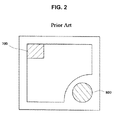
- FIG. 2 is a view illustrating one example of an electrode structure disclosed in US Patent 5,563,422 .
- a p-side bonding pad 700 and an n-side electrode 800 are positioned at corner portions of a light emitting device in a diagonal direction.
- the p-side bonding pad 700 and the n-side electrode 800 are positioned in the farthest portions in the light emitting device to thereby improve current spreading.
- FIG. 3 is a view illustrating one example of an electrode structure disclosed in US Patent 6,307,218 .
- finger electrodes 710 and 810 are provided between a p-side bonding pad 700 and an n-side electrode 800 at regular intervals, thereby improving current spreading.
- an object of the present invention is to provide a semiconductor light emitting device which can improve current spreading.
- Another object of the present invention is to provide a semiconductor light emitting device which can evenly emit light.
- Another object of the present invention is to provide a semiconductor light emitting device which can extend a lifespan.
- Another object of the present invention is to provide a semiconductor light emitting device which can evenly emit light over a wide light emission area.
- a semiconductor light emitting device generating light by recombination of electrons and holes, the semiconductor light emitting device, including: a first finger electrode for supplying one of the electrons and holes; a second finger electrode supplying the other of the electrons and holes, and spaced apart from the first finger electrode at a first interval; and a third finger electrode electrically connected to the first finger electrode, and spaced apart from the second finger electrode at a second interval which is smaller than the first interval.
- the semiconductor light emitting device includes a fourth finger electrode electrically connected to the second finger electrode, and spaced apart from the third finger electrode at a third interval which is smaller than the first interval.
- the third interval is smaller than the second interval.
- the first finger electrode is positioned in the outermost portion of the light emitting device.
- the first finger electrode supplies the holes.
- the semiconductor light emitting device is a III-nitride semiconductor light emitting device.
- a semiconductor light emitting device generating light by recombination of electrons and holes, the semiconductor light emitting device, including: a plurality of finger electrodes for supplying one of the electrons and holes; and at least one further finger electrode supplying the other of the electrons and holes, and alternately arranged with the plurality of finger electrodes, an interval between the at least one further finger electrode and the finger electrode positioned in the outermost portion of the light emitting device among the plurality of finger electrodes being larger than the other intervals.
- the other intervals are gradually reduced toward the inside of the light emitting device.
- the plurality of finger electrodes supply the holes.
- the plurality of finger electrodes supply the holes
- the semiconductor light emitting device is a III-nitride semiconductor light emitting device.
- the current spreading can be improved.
- light can be evenly emitted.
- lifespan of the device can be extended.
- light can be evenly emit over a wide emission area.
- FIG. 4 is a view illustrating an example of a structure of electrodes arranged at regular intervals.
- a p-side bonding pad 70 and an n-side electrode 80 are provided.
- Finger electrodes 71, 72 and 73 extend from the p-side bonding pad 70
- finger electrodes 81 and 82 extend from the n-side electrode 80.
- the finger electrodes 71, 72 and 73 and the finger electrodes 81 and 82 are alternately positioned to supply the current to an entire light emitting device. Intervals a, b, c and d between the finger electrodes 71, 72 and 73 and the finger electrodes 81 and 82 are maintained to be constant.
- FIG. 5 is a view illustrating light emission distributions in a light emitting device with the electrode structure of FIG. 4 , particularly, light emission distributions when 200 mA, 300 mA and 400 mA of currents are supplied to the same light emitting device.
- the intervals a, b, c and d are maintained at about 89 ⁇ m.
- the light emission between the finger electrode 71 extending from the p-side bonding pad 70 and the finger electrode 81 extending from the n-side electrode 80 is more intense than the light emission between the finger electrode 81 and the finger electrode 72, the light emission between the finger electrode 72 and the finger electrode 82, and the light emission between the finger electrode 82 and the finger electrode 73.
- the concentration of the light emission and the non-uniformity of the current density may have a detrimental effect on the entire light emission efficiency and lifespan of the light emitting device. Therefore, such problems should be solved.
- the supplied current increases (generally, when an area of a light emitting device is large, a supplied current is high), the concentration phenomenon becomes serious. Accordingly, the current concentration phenomenon can be a problem particularly in a large-sized light emitting device.
- FIG. 6 is a view illustrating an example of an electrode structure according to the present invention.
- a p-side bonding pad 70 and an n-side electrode 80 are provided.
- Finger electrodes 71, 72 and 73 extend from the p-side bonding pad 70
- finger electrodes 81 and 82 extend from the n-side electrode 80.
- the finger electrodes 71, 72 and 73 and the finger electrodes 81 and 82 are alternately positioned to supply the current to an entire light emitting device.
- intervals a, b, c and d between the finger electrodes 71, 72 and 73 and the finger electrodes 81 and 82 are relatively reduced toward the inside of the light emitting device.
- FIG. 7 is a view illustrating light emission distributions in a light emitting device with the electrode structure of FIG. 6 , particularly, light emission distributions when 200 mA, 300 mA and 400 mA of currents are supplied to the same light emitting device.
- the intervals a, b, c and d (refer to FIG. 6 ) are 118 ⁇ m, 88 ⁇ m, 79 ⁇ m and 70 ⁇ m, respectively.
- the light emission between the finger electrode 71 and the finger electrode 81, the light emission between the finger electrode 81 and the finger electrode 72, the light emission between the finger electrode 72 and the finger electrode 82, and the light emission between the finger electrode 82 and the finger electrode 73 are even. That is, the light emission distributions of the light emitting device can be uniformized by adjusting the intervals between the finger electrodes. When 400 mA of current is supplied, the light emission between the finger electrode 82 and the finger electrode 73 is intensified. It can be solved by slightly widening the interval d. Therefore, it should not be construed that the technical ideas of the present invention are limited to gradual reduction of the intervals a, b, c and d.
- the present invention in order to overcome the light emission concentration or current concentration occurring when the finger electrodes are arranged at regular intervals, relatively widens an interval in a light emission concentration region, and sets up a narrower interval in a weak light emission region than in an appropriate light emission region in terms of the light emission distribution.
- the p-side bonding pad 70 and the finger electrode 71 are positioned at the outermost portions of the light emitting device, and the n-side electrode 80 and the finger electrode 81 are positioned inwardly.
- the n-side electrode 80 and the finger electrode 81 that need to be etched are positioned at the outermost portions of the light emitting device, since the light emitting device are to be etched, a light emission area is reduced.
- the p-side bonding pad 70 and the finger electrode 71 formed on the light emitting device without needing an etching are positioned at the outermost portions thereof, there is a further advantage of preventing the reduction of the light emission area.
Abstract
Description
- The present invention relates to a semiconductor light emitting device, and more particularly, to a semiconductor light emitting device with an electrode structure capable of evenly emitting light.
- The III-nitride semiconductor light emitting device means a light emitting device such as a light emitting diode including a compound semiconductor layer composed of Al(x)Ga(y)In(1-x-y)N (0≤x≤1, 0≤y≤1, 0≤x+y≤1), and may further include a material composed of other group elements, such as SiC, SiN, SiCN and CN, and a semiconductor layer made of such materials.
-
FIG. 1 is a view illustrating one example of a conventional III-nitride semiconductor light emitting device. The III-nitride semiconductor light emitting device includes asubstrate 100, abuffer layer 200 grown on thesubstrate 100, an n-typenitride semiconductor layer 300 grown on thebuffer layer 200, anactive layer 400 grown on the n-typenitride semiconductor layer 300, a p-typenitride semiconductor layer 500 grown on theactive layer 400, a p-side electrode 600 formed on the p-typenitride semiconductor layer 500, a p-side bonding pad 700 formed on the p-side electrode 600, an n-side electrode 800 formed on the n-type nitride semiconductor layer exposed by mesa-etching the p-typenitride semiconductor layer 500 and theactive layer 400, and aprotective film 900. - In the case of the
substrate 100, a GaN substrate can be used as a homo-substrate, and a sapphire substrate, a SiC substrate or a Si substrate can be used as a hetero-substrate. However, any type of substrate that can grow a nitride semiconductor layer thereon can be employed. In the case that the SiC substrate is used, the n-side electrode 800 can be formed on the side of the SiC substrate. - The nitride semiconductor layers epitaxially grown on the
substrate 100 are grown usually by metal organic chemical vapor deposition (MOCVD). - The
buffer layer 200 serves to overcome differences in lattice constant and thermal expansion coefficient between the hetero-substrate 100 and the nitride semiconductor layers.U.S. Pat. No. 5,122,845 discloses a technique of growing an AlN buffer layer with a thickness of 100 to 500 Å on a sapphire substrate at 380 to 800 °C. In addition,U.S. Pat. No. 5,290,393 discloses a technique of growing an Al(x)Ga(1-x)N (0≤x<1) buffer layer with a thickness of 10 to 5000 Å on a sapphire substrate at 200 to 900 °C. Moreover,PCT Publication No. WO/05/053042 - In the n-type
nitride semiconductor layer 300, at least the n-side electrode 800 formed region (n-type contact layer) is doped with a dopant. Preferably, the n-type contact layer is made of GaN and doped with Si.U.S. Pat. No. 5,733,796 discloses a technique of doping an n-type contact layer at a target doping concentration by adjusting the mixture ratio of Si and other source materials. - The
active layer 400 generates light quanta (light) by recombination of electrons and holes. Normally, theactive layer 400 contains In(x)Ga(1-x)N (0<x≤1) and has single or multi-quantum well layers.PCT Publication No. WO/02/021121 - The p-type
nitride semiconductor layer 500 is doped with an appropriate dopant such as Mg, and has p-type conductivity by an activation process.U.S. Pat. No. 5,247,533 discloses a technique of activating a p-type nitride semiconductor layer by electron beam irradiation. Moreover,U.S. Pat. No. 5,306,662 discloses a technique of activating a p-type nitride semiconductor layer by annealing over 400 °C.PCT Publication No. WO/05/022655 - The p-
side electrode 600 is provided to facilitate current supply to the p-typenitride semiconductor layer 500.U.S. Pat. No. 5,563,422 discloses a technique associated with a light transmitting electrode composed of Ni and Au and formed almost on the entire surface of the p-typenitride semiconductor layer 500 and in ohmic-contact with the p-typenitride semiconductor layer 500. In addition,U.S. Pat. No. 6,515,306 discloses a technique of forming an n-type superlattice layer on a p-type nitride semiconductor layer, and forming a light transmitting electrode made of ITO thereon. - Meanwhile, the
light transmitting electrode 600 can be formed thick not to transmit but to reflect light toward thesubstrate 100. This technique is called a flip chip technique.U.S. Pat. No. 6,194,743 discloses a technique associated with an electrode structure including an Ag layer with a thickness over 20 nm, a diffusion barrier layer covering the Ag layer, and a bonding layer containing Au and Al, and covering the diffusion barrier layer. - The p-
side bonding pad 700 and the n-side electrode 800 are provided for current supply and external wire bonding.U.S. Pat. No. 5,563,422 discloses a technique of forming an n-side electrode with Ti and Al. - The
protection film 900 can be made of SiO2, and may be omitted. - In the meantime, the n-type
nitride semiconductor layer 300 or the p-typenitride semiconductor layer 500 can be constructed as single or plural layers. Recently, a technology of manufacturing vertical light emitting devices is introduced by separating thesubstrate 100 from the nitride semiconductor layers using laser technique or wet etching. -
FIG. 2 is a view illustrating one example of an electrode structure disclosed inUS Patent 5,563,422 . A p-side bonding pad 700 and an n-side electrode 800 are positioned at corner portions of a light emitting device in a diagonal direction. The p-side bonding pad 700 and the n-side electrode 800 are positioned in the farthest portions in the light emitting device to thereby improve current spreading. -
FIG. 3 is a view illustrating one example of an electrode structure disclosed inUS Patent 6,307,218 . According to a tendency toward light emitting devices with large size,finger electrodes side bonding pad 700 and an n-side electrode 800 at regular intervals, thereby improving current spreading. - Accordingly, the present invention has been made to solve the above-described shortcomings occurring in the prior art, and an object of the present invention is to provide a semiconductor light emitting device which can improve current spreading.
- Another object of the present invention is to provide a semiconductor light emitting device which can evenly emit light.
- Yet, another object of the present invention is to provide a semiconductor light emitting device which can extend a lifespan.
- Yet, another object of the present invention is to provide a semiconductor light emitting device which can evenly emit light over a wide light emission area.
- To this end, there is provided a semiconductor light emitting device generating light by recombination of electrons and holes, the semiconductor light emitting device, including: a first finger electrode for supplying one of the electrons and holes; a second finger electrode supplying the other of the electrons and holes, and spaced apart from the first finger electrode at a first interval; and a third finger electrode electrically connected to the first finger electrode, and spaced apart from the second finger electrode at a second interval which is smaller than the first interval.
- Also, in another aspect of the present invention, the semiconductor light emitting device includes a fourth finger electrode electrically connected to the second finger electrode, and spaced apart from the third finger electrode at a third interval which is smaller than the first interval.
- Also, in another aspect of the present invention, the third interval is smaller than the second interval.
- Also, in another aspect of the present invention, the first finger electrode is positioned in the outermost portion of the light emitting device.
- Also, in another aspect of the present invention, the first finger electrode supplies the holes.
- Also, in another aspect of the present invention, the semiconductor light emitting device is a III-nitride semiconductor light emitting device.
- Also, in another aspect of the present invention, there is provided a semiconductor light emitting device generating light by recombination of electrons and holes, the semiconductor light emitting device, including: a plurality of finger electrodes for supplying one of the electrons and holes; and at least one further finger electrode supplying the other of the electrons and holes, and alternately arranged with the plurality of finger electrodes, an interval between the at least one further finger electrode and the finger electrode positioned in the outermost portion of the light emitting device among the plurality of finger electrodes being larger than the other intervals.
- Also, in another aspect of the present invention, the other intervals are gradually reduced toward the inside of the light emitting device.
- Also, in another aspect of the present invention, the plurality of finger electrodes supply the holes.
- Also, in another aspect of the present invention, the plurality of finger electrodes supply the holes, and the semiconductor light emitting device is a III-nitride semiconductor light emitting device.
- According to a semiconductor light emitting device of the present invention, the current spreading can be improved.
- Also, according to a semiconductor light emitting device of the present invention, light can be evenly emitted.
- Also, according to a semiconductor light emitting device of the present invention, lifespan of the device can be extended.
- Also, according to a semiconductor light emitting device of the present invention, light can be evenly emit over a wide emission area.
-
-
FIG. 1 is a view illustrating one example of a conventional III-nitride semiconductor light emitting device. -
FIG. 2 is a view illustrating one example of an electrode structure disclosed inUS Patent 5,563,422 . -
FIG. 3 is a view illustrating one example of an electrode structure disclosed inUS Patent 6,307,218 . -
FIG. 4 is a view illustrating one example of a structure of electrodes arranged at regular intervals. -
FIG. 5 is a view illustrating light emission distributions in a light emitting device with the electrode structure ofFIG. 4 . -
FIG. 6 is a view illustrating one example of an electrode structure according to the present invention. -
FIG. 7 is a view illustrating light emission distributions in a light emitting device with the electrode structure ofFIG. 6 . - Hereinafter, the present invention will be described in detail with reference to the accompanying drawings.
-
FIG. 4 is a view illustrating an example of a structure of electrodes arranged at regular intervals. A p-side bonding pad 70 and an n-side electrode 80 are provided.Finger electrodes 71, 72 and 73 extend from the p-side bonding pad 70, andfinger electrodes 81 and 82 extend from the n-side electrode 80. Thefinger electrodes 71, 72 and 73 and thefinger electrodes 81 and 82 are alternately positioned to supply the current to an entire light emitting device. Intervals a, b, c and d between thefinger electrodes 71, 72 and 73 and thefinger electrodes 81 and 82 are maintained to be constant. -
FIG. 5 is a view illustrating light emission distributions in a light emitting device with the electrode structure ofFIG. 4 , particularly, light emission distributions when 200 mA, 300 mA and 400 mA of currents are supplied to the same light emitting device. Here, the intervals a, b, c and d (refer toFIG. 4 ) are maintained at about 89 µm. The light emission between thefinger electrode 71 extending from the p-side bonding pad 70 and thefinger electrode 81 extending from the n-side electrode 80 is more intense than the light emission between thefinger electrode 81 and the finger electrode 72, the light emission between the finger electrode 72 and the finger electrode 82, and the light emission between the finger electrode 82 and the finger electrode 73. The concentration of the light emission and the non-uniformity of the current density may have a detrimental effect on the entire light emission efficiency and lifespan of the light emitting device. Therefore, such problems should be solved. InFIG. 4 , when the supplied current increases (generally, when an area of a light emitting device is large, a supplied current is high), the concentration phenomenon becomes serious. Accordingly, the current concentration phenomenon can be a problem particularly in a large-sized light emitting device. -
FIG. 6 is a view illustrating an example of an electrode structure according to the present invention. A p-side bonding pad 70 and an n-side electrode 80 are provided.Finger electrodes 71, 72 and 73 extend from the p-side bonding pad 70, andfinger electrodes 81 and 82 extend from the n-side electrode 80. Thefinger electrodes 71, 72 and 73 and thefinger electrodes 81 and 82 are alternately positioned to supply the current to an entire light emitting device. In a state where the p-side bonding pad 70 and the n-side electrode 80 are maintained as they are in the light emitting device ofFIG. 4 , intervals a, b, c and d between thefinger electrodes 71, 72 and 73 and thefinger electrodes 81 and 82 are relatively reduced toward the inside of the light emitting device. -
FIG. 7 is a view illustrating light emission distributions in a light emitting device with the electrode structure ofFIG. 6 , particularly, light emission distributions when 200 mA, 300 mA and 400 mA of currents are supplied to the same light emitting device. Here, the intervals a, b, c and d (refer toFIG. 6 ) are 118 µm, 88 µm, 79 µm and 70 µm, respectively. As compared with the light emission distributions ofFIG. 5 , the light emission between thefinger electrode 71 and thefinger electrode 81, the light emission between thefinger electrode 81 and the finger electrode 72, the light emission between the finger electrode 72 and the finger electrode 82, and the light emission between the finger electrode 82 and the finger electrode 73 are even. That is, the light emission distributions of the light emitting device can be uniformized by adjusting the intervals between the finger electrodes. When 400 mA of current is supplied, the light emission between the finger electrode 82 and the finger electrode 73 is intensified. It can be solved by slightly widening the interval d. Therefore, it should not be construed that the technical ideas of the present invention are limited to gradual reduction of the intervals a, b, c and d. That is, in order to overcome the light emission concentration or current concentration occurring when the finger electrodes are arranged at regular intervals, the present invention relatively widens an interval in a light emission concentration region, and sets up a narrower interval in a weak light emission region than in an appropriate light emission region in terms of the light emission distribution. - In the light emitting device of
FIG. 6 , preferably, the p-side bonding pad 70 and thefinger electrode 71 are positioned at the outermost portions of the light emitting device, and the n-side electrode 80 and thefinger electrode 81 are positioned inwardly. In a case where the n-side electrode 80 and thefinger electrode 81 that need to be etched are positioned at the outermost portions of the light emitting device, since the light emitting device are to be etched, a light emission area is reduced. However, when the p-side bonding pad 70 and thefinger electrode 71 formed on the light emitting device without needing an etching are positioned at the outermost portions thereof, there is a further advantage of preventing the reduction of the light emission area.
Claims (10)
- A semiconductor light emitting device generating light by recombination of electrons and holes, the semiconductor light emitting device comprising:a first finger electrode (71) for supplying one of the electrons and holes;a second finger electrode (81) supplying the other of the electrons and holes, and spaced apart from the first finger electrode (71) at a first interval (a); anda third finger electrode (72) electrically connected to the first finger electrode (71), and spaced apart from the second finger electrode (81) at a second interval (b) which is smaller than the first interval (a).
- The semiconductor light emitting device of Claim 1, comprising:a fourth finger electrode (82) electrically connected to the second finger electrode (81), and spaced apart from the third finger electrode (72) at a third interval (c) which is smaller than the first interval (a).
- The semiconductor light emitting device of Claim 2, wherein the third interval (c) is smaller than the second interval (b).
- The semiconductor light emitting device of Claim 1, wherein the first finger electrode (71) is positioned in the outermost portion of the light emitting device.
- The semiconductor light emitting device of Claim 4, wherein the first finger electrode (71) supplies the holes.
- The semiconductor light emitting device of Claim 2, wherein the semiconductor light emitting device is a III-nitride semiconductor light emitting device.
- A semiconductor light emitting device generating light by recombination of electrons and holes, the semiconductor light emitting device comprising:a plurality of finger electrodes (71, 72, 73) for supplying one of the electrons and holes; andat least one further finger electrode (81, 82) supplying the other of the electrons and holes, and alternately arranged with the plurality of finger electrodes (71, 72, 73),wherein an interval (a) between the at least one further finger electrode (81, 82) and the finger electrode (71) among the plurality of finger electrodes (71, 72, 73) positioned in the outermost portion of the light emitting device is larger than the other intervals (b, c, d).
- The semiconductor light emitting device of Claim 7, wherein the other intervals (b, c, d) are gradually reduced toward the inside of the light emitting device.
- The semiconductor light emitting device of Claim 7, wherein the plurality of finger electrodes (71, 72, 73) supply the holes.
- The semiconductor light emitting device of Claim 8, wherein the plurality of finger electrodes (71, 72, 73) supply the holes, the semiconductor light emitting device being a III-nitride semiconductor light emitting device.
Applications Claiming Priority (1)
| Application Number | Priority Date | Filing Date | Title |
|---|---|---|---|
| KR1020080045182A KR100988041B1 (en) | 2008-05-15 | 2008-05-15 | Semiconductor light emitting device |
Publications (2)
| Publication Number | Publication Date |
|---|---|
| EP2120273A2 true EP2120273A2 (en) | 2009-11-18 |
| EP2120273A3 EP2120273A3 (en) | 2011-03-02 |
Family
ID=40888128
Family Applications (1)
| Application Number | Title | Priority Date | Filing Date |
|---|---|---|---|
| EP08162753A Withdrawn EP2120273A3 (en) | 2008-05-15 | 2008-08-21 | Semiconductor light emitting device |
Country Status (6)
| Country | Link |
|---|---|
| US (1) | US7795610B2 (en) |
| EP (1) | EP2120273A3 (en) |
| JP (1) | JP2009278056A (en) |
| KR (1) | KR100988041B1 (en) |
| CN (1) | CN101582474B (en) |
| TW (1) | TW200947753A (en) |
Families Citing this family (28)
| Publication number | Priority date | Publication date | Assignee | Title |
|---|---|---|---|---|
| US6633120B2 (en) * | 1998-11-19 | 2003-10-14 | Unisplay S.A. | LED lamps |
| USD668234S1 (en) * | 2001-05-24 | 2012-10-02 | Lextar Electornics Corp. | LED chip |
| US9640737B2 (en) | 2011-01-31 | 2017-05-02 | Cree, Inc. | Horizontal light emitting diodes including phosphor particles |
| US9660153B2 (en) | 2007-11-14 | 2017-05-23 | Cree, Inc. | Gap engineering for flip-chip mounted horizontal LEDs |
| US9754926B2 (en) * | 2011-01-31 | 2017-09-05 | Cree, Inc. | Light emitting diode (LED) arrays including direct die attach and related assemblies |
| TWI376817B (en) * | 2007-11-23 | 2012-11-11 | Epistar Corp | Light emitting device, light source apparatus and backlight module |
| KR100941616B1 (en) * | 2008-05-15 | 2010-02-11 | 주식회사 에피밸리 | Semiconductor light emitting device |
| JP5443286B2 (en) * | 2009-12-24 | 2014-03-19 | スタンレー電気株式会社 | Face-up type optical semiconductor device |
| KR100977682B1 (en) * | 2010-01-15 | 2010-08-24 | (주)더리즈 | Semiconductor light emitting device |
| BR112013001623B1 (en) * | 2010-07-23 | 2021-02-02 | Nichia Corporation | light emitting element |
| US9171883B2 (en) | 2010-08-30 | 2015-10-27 | Epistar Corporation | Light emitting device |
| KR101249924B1 (en) * | 2010-11-03 | 2013-04-03 | (주)버티클 | Semiconductor devices and fabrication method thereof |
| US9673363B2 (en) | 2011-01-31 | 2017-06-06 | Cree, Inc. | Reflective mounting substrates for flip-chip mounted horizontal LEDs |
| US9831220B2 (en) | 2011-01-31 | 2017-11-28 | Cree, Inc. | Light emitting diode (LED) arrays including direct die attach and related assemblies |
| JP5741164B2 (en) * | 2011-04-12 | 2015-07-01 | 日亜化学工業株式会社 | Light emitting element |
| CN102185066A (en) * | 2011-04-26 | 2011-09-14 | 中国科学院苏州纳米技术与纳米仿生研究所 | High-power LED (light emitting diode) with improved structure |
| US10243121B2 (en) | 2011-06-24 | 2019-03-26 | Cree, Inc. | High voltage monolithic LED chip with improved reliability |
| JP5754269B2 (en) * | 2011-07-07 | 2015-07-29 | 日亜化学工業株式会社 | Light emitting element |
| USD698743S1 (en) | 2012-12-07 | 2014-02-04 | Epistar Corporation | Light-emitting diode |
| CN104183682A (en) * | 2013-05-27 | 2014-12-03 | 崴发控股有限公司 | Flip-chip light-emitting diode element and packaging structure thereof |
| USD721663S1 (en) | 2013-08-02 | 2015-01-27 | Epistar Corporation | Light-emitting diode device |
| CN104377287B (en) * | 2013-08-14 | 2017-04-26 | 展晶科技(深圳)有限公司 | Light-emitting diode and manufacturing method thereof |
| USD743355S1 (en) * | 2014-07-22 | 2015-11-17 | Epistar Corporation | Light-emitting diode unit |
| TWD169527S (en) * | 2014-08-20 | 2015-08-01 | 晶元光電股份有限公司 | Portions of light-emitting diode unit |
| EP3062354B1 (en) | 2015-02-26 | 2020-10-14 | Nichia Corporation | Light emitting element |
| TWI632698B (en) * | 2015-10-02 | 2018-08-11 | 晶元光電股份有限公司 | Light-emitting device |
| CN105226177B (en) * | 2015-10-13 | 2018-03-02 | 厦门市三安光电科技有限公司 | The eutectic electrode structure and flip LED chips of flip LED chips |
| WO2022004393A1 (en) * | 2020-07-02 | 2022-01-06 | ヌヴォトンテクノロジージャパン株式会社 | Nitride semiconductor light emitting element |
Citations (12)
| Publication number | Priority date | Publication date | Assignee | Title |
|---|---|---|---|---|
| US5122845A (en) | 1989-03-01 | 1992-06-16 | Toyoda Gosei Co., Ltd. | Substrate for growing gallium nitride compound-semiconductor device and light emitting diode |
| US5247533A (en) | 1990-12-26 | 1993-09-21 | Toyoda Gosei Co., Ltd. | Gallium nitride group compound semiconductor laser diode |
| US5290393A (en) | 1991-01-31 | 1994-03-01 | Nichia Kagaku Kogyo K.K. | Crystal growth method for gallium nitride-based compound semiconductor |
| US5306662A (en) | 1991-11-08 | 1994-04-26 | Nichia Chemical Industries, Ltd. | Method of manufacturing P-type compound semiconductor |
| US5563422A (en) | 1993-04-28 | 1996-10-08 | Nichia Chemical Industries, Ltd. | Gallium nitride-based III-V group compound semiconductor device and method of producing the same |
| US5733796A (en) | 1990-02-28 | 1998-03-31 | Toyoda Gosei Co., Ltd. | Light-emitting semiconductor device using gallium nitride group compound |
| US6194743B1 (en) | 1997-12-15 | 2001-02-27 | Agilent Technologies, Inc. | Nitride semiconductor light emitting device having a silver p-contact |
| US6307218B1 (en) | 1998-11-20 | 2001-10-23 | Lumileds Lighting, U.S., Llc | Electrode structures for light emitting devices |
| WO2002021121A1 (en) | 2000-09-08 | 2002-03-14 | Dow Global Technolgies Inc. | Sequential detection ion chromatography |
| US6515306B2 (en) | 2001-01-19 | 2003-02-04 | South Epitaxy Corporation | Light emitting diode |
| WO2005022655A1 (en) | 2003-09-03 | 2005-03-10 | Epivalley Co., Ltd. | Algainn based optical device and fabrication method thereof |
| WO2005053042A1 (en) | 2003-11-28 | 2005-06-09 | Epivalley Co., Ltd. | Method for fabricating gan-based nitride layer |
Family Cites Families (9)
| Publication number | Priority date | Publication date | Assignee | Title |
|---|---|---|---|---|
| JP2828187B2 (en) * | 1993-04-08 | 1998-11-25 | 日亜化学工業株式会社 | Gallium nitride based compound semiconductor light emitting device |
| WO2001073858A1 (en) * | 2000-03-31 | 2001-10-04 | Toyoda Gosei Co., Ltd. | Group-iii nitride compound semiconductor device |
| JP4810746B2 (en) | 2000-03-31 | 2011-11-09 | 豊田合成株式会社 | Group III nitride compound semiconductor device |
| JP4053926B2 (en) | 2002-05-27 | 2008-02-27 | 日亜化学工業株式会社 | Nitride semiconductor light emitting device and light emitting device using the same |
| US20060284191A1 (en) * | 2005-06-16 | 2006-12-21 | Epistar Corporation | Light emitting diode |
| JP4404097B2 (en) * | 2006-02-06 | 2010-01-27 | 日亜化学工業株式会社 | Semiconductor light emitting device |
| KR100833309B1 (en) * | 2006-04-04 | 2008-05-28 | 삼성전기주식회사 | Nitride semiconductor light emitting device |
| KR100813597B1 (en) * | 2006-06-22 | 2008-03-17 | 삼성전기주식회사 | Nitride semiconductor light emitting device |
| US8698193B2 (en) * | 2008-07-29 | 2014-04-15 | Sharp Kabushiki Kaisha | Light emitting device and method for manufacturing the same |
-
2008
- 2008-05-15 KR KR1020080045182A patent/KR100988041B1/en not_active IP Right Cessation
- 2008-08-21 US US12/195,741 patent/US7795610B2/en not_active Expired - Fee Related
- 2008-08-21 EP EP08162753A patent/EP2120273A3/en not_active Withdrawn
- 2008-08-26 CN CN2008102124395A patent/CN101582474B/en not_active Expired - Fee Related
- 2008-09-16 JP JP2008236302A patent/JP2009278056A/en active Pending
- 2008-09-25 TW TW097136810A patent/TW200947753A/en unknown
Patent Citations (12)
| Publication number | Priority date | Publication date | Assignee | Title |
|---|---|---|---|---|
| US5122845A (en) | 1989-03-01 | 1992-06-16 | Toyoda Gosei Co., Ltd. | Substrate for growing gallium nitride compound-semiconductor device and light emitting diode |
| US5733796A (en) | 1990-02-28 | 1998-03-31 | Toyoda Gosei Co., Ltd. | Light-emitting semiconductor device using gallium nitride group compound |
| US5247533A (en) | 1990-12-26 | 1993-09-21 | Toyoda Gosei Co., Ltd. | Gallium nitride group compound semiconductor laser diode |
| US5290393A (en) | 1991-01-31 | 1994-03-01 | Nichia Kagaku Kogyo K.K. | Crystal growth method for gallium nitride-based compound semiconductor |
| US5306662A (en) | 1991-11-08 | 1994-04-26 | Nichia Chemical Industries, Ltd. | Method of manufacturing P-type compound semiconductor |
| US5563422A (en) | 1993-04-28 | 1996-10-08 | Nichia Chemical Industries, Ltd. | Gallium nitride-based III-V group compound semiconductor device and method of producing the same |
| US6194743B1 (en) | 1997-12-15 | 2001-02-27 | Agilent Technologies, Inc. | Nitride semiconductor light emitting device having a silver p-contact |
| US6307218B1 (en) | 1998-11-20 | 2001-10-23 | Lumileds Lighting, U.S., Llc | Electrode structures for light emitting devices |
| WO2002021121A1 (en) | 2000-09-08 | 2002-03-14 | Dow Global Technolgies Inc. | Sequential detection ion chromatography |
| US6515306B2 (en) | 2001-01-19 | 2003-02-04 | South Epitaxy Corporation | Light emitting diode |
| WO2005022655A1 (en) | 2003-09-03 | 2005-03-10 | Epivalley Co., Ltd. | Algainn based optical device and fabrication method thereof |
| WO2005053042A1 (en) | 2003-11-28 | 2005-06-09 | Epivalley Co., Ltd. | Method for fabricating gan-based nitride layer |
Also Published As
| Publication number | Publication date |
|---|---|
| TW200947753A (en) | 2009-11-16 |
| KR100988041B1 (en) | 2010-10-18 |
| US7795610B2 (en) | 2010-09-14 |
| US20090283789A1 (en) | 2009-11-19 |
| CN101582474A (en) | 2009-11-18 |
| KR20090119255A (en) | 2009-11-19 |
| JP2009278056A (en) | 2009-11-26 |
| EP2120273A3 (en) | 2011-03-02 |
| CN101582474B (en) | 2011-06-29 |
Similar Documents
| Publication | Publication Date | Title |
|---|---|---|
| EP2120273A2 (en) | Semiconductor light emitting device | |
| US8835902B2 (en) | Nano-structured light-emitting devices | |
| US20110062487A1 (en) | Semiconductor light emitting device | |
| EP2045845A2 (en) | III-nitride semiconductor light emitting device | |
| JP4503570B2 (en) | Nitride semiconductor device | |
| US20100140656A1 (en) | Semiconductor Light-Emitting Device | |
| US20110001158A1 (en) | Iii-nitride semiconductor light emitting device | |
| KR101100684B1 (en) | Iii nitride semiconductor light emitting device | |
| US8759815B2 (en) | Nitride based semiconductor light emitting device | |
| US7253451B2 (en) | III-nitride semiconductor light emitting device | |
| CN101478021B (en) | III-nitride semiconductor light emitting device | |
| US20110233603A1 (en) | Semiconductor light-emitting device | |
| KR100661960B1 (en) | Light emitting diode and manufacturing method thereof | |
| KR100997908B1 (en) | ?-nitride semiconductor light emitting device | |
| KR20090073949A (en) | Manufacturing method of iii-nitride semiconductor light emitting device | |
| KR20100012003A (en) | Iii-nitride semiconductor light emitting device | |
| KR101197686B1 (en) | Iii-nitride semiconductor light emitting device | |
| US20100102338A1 (en) | III-Nitride Semiconductor Light Emitting Device | |
| KR20110139592A (en) | Light emitting device | |
| KR20100120102A (en) | Semiconductor light emitting device | |
| WO2009154409A2 (en) | Semiconductor light emitting device | |
| WO2007024122A1 (en) | Semiconductor light emitting device | |
| KR20060037578A (en) | Iii-nitride semiconductor light emitting device | |
| KR20110007293A (en) | Method of forming iii-nitride semiconductor light emitting device | |
| KR20070038794A (en) | Iii-nitride semiconductor light emitting device |
Legal Events
| Date | Code | Title | Description |
|---|---|---|---|
| PUAI | Public reference made under article 153(3) epc to a published international application that has entered the european phase |
Free format text: ORIGINAL CODE: 0009012 |
|
| AK | Designated contracting states |
Kind code of ref document: A2 Designated state(s): AT BE BG CH CY CZ DE DK EE ES FI FR GB GR HR HU IE IS IT LI LT LU LV MC MT NL NO PL PT RO SE SI SK TR |
|
| AX | Request for extension of the european patent |
Extension state: AL BA MK RS |
|
| PUAL | Search report despatched |
Free format text: ORIGINAL CODE: 0009013 |
|
| AK | Designated contracting states |
Kind code of ref document: A3 Designated state(s): AT BE BG CH CY CZ DE DK EE ES FI FR GB GR HR HU IE IS IT LI LT LU LV MC MT NL NO PL PT RO SE SI SK TR |
|
| AX | Request for extension of the european patent |
Extension state: AL BA MK RS |
|
| 17P | Request for examination filed |
Effective date: 20110902 |
|
| AKX | Designation fees paid |
Designated state(s): DE |
|
| STAA | Information on the status of an ep patent application or granted ep patent |
Free format text: STATUS: THE APPLICATION IS DEEMED TO BE WITHDRAWN |
|
| 18D | Application deemed to be withdrawn |
Effective date: 20130301 |