EP2132748B1 - Decoding control with address transition detection in page erase function - Google Patents
Decoding control with address transition detection in page erase function Download PDFInfo
- Publication number
- EP2132748B1 EP2132748B1 EP08714575.1A EP08714575A EP2132748B1 EP 2132748 B1 EP2132748 B1 EP 2132748B1 EP 08714575 A EP08714575 A EP 08714575A EP 2132748 B1 EP2132748 B1 EP 2132748B1
- Authority
- EP
- European Patent Office
- Prior art keywords
- address
- page
- block
- circuit
- reset
- Prior art date
- Legal status (The legal status is an assumption and is not a legal conclusion. Google has not performed a legal analysis and makes no representation as to the accuracy of the status listed.)
- Not-in-force
Links
Images


Classifications
-
- G—PHYSICS
- G11—INFORMATION STORAGE
- G11C—STATIC STORES
- G11C16/00—Erasable programmable read-only memories
- G11C16/02—Erasable programmable read-only memories electrically programmable
- G11C16/06—Auxiliary circuits, e.g. for writing into memory
- G11C16/08—Address circuits; Decoders; Word-line control circuits
-
- G—PHYSICS
- G11—INFORMATION STORAGE
- G11C—STATIC STORES
- G11C16/00—Erasable programmable read-only memories
- G11C16/02—Erasable programmable read-only memories electrically programmable
- G11C16/06—Auxiliary circuits, e.g. for writing into memory
- G11C16/10—Programming or data input circuits
- G11C16/14—Circuits for erasing electrically, e.g. erase voltage switching circuits
- G11C16/16—Circuits for erasing electrically, e.g. erase voltage switching circuits for erasing blocks, e.g. arrays, words, groups
-
- G—PHYSICS
- G11—INFORMATION STORAGE
- G11C—STATIC STORES
- G11C8/00—Arrangements for selecting an address in a digital store
- G11C8/10—Decoders
-
- G—PHYSICS
- G11—INFORMATION STORAGE
- G11C—STATIC STORES
- G11C8/00—Arrangements for selecting an address in a digital store
- G11C8/12—Group selection circuits, e.g. for memory block selection, chip selection, array selection
-
- G—PHYSICS
- G11—INFORMATION STORAGE
- G11C—STATIC STORES
- G11C8/00—Arrangements for selecting an address in a digital store
- G11C8/20—Address safety or protection circuits, i.e. arrangements for preventing unauthorized or accidental access
Definitions
- the invention relates to page erase functions in flash memories.
- An erase function is used in non-volatile flash memory to restore the original state of a flash cell. Due to physical limitations of the erase operation, it takes a long time to complete the operation. The erase operation takes relatively longer than other main operations such as a page program. For example, where the erase time might be 1.5ms, the page program time might be 25us.
- a block erase operation an entire block is erased at once, a block consisting of a set of pages (rows). Because of this, block erase needs to backup the contents to another memory medium before erasing all contents in the selected block at the same time so as to enable some of the contents (certain pages) to be restored assuming some of the contents of the block should be kept. This requires another memory system to be incorporated in the same board or the same package to support the mentioned data restoration of flash memory. This increases the total system cost with flash memory and makes the data control more complicated.
- Patent Publication US-A-5784327 discloses an EEPROM operation method wherein erasure is performed on one or more pages in a non-volatile from memory and wherein registers after each page- or block erasure are reset.
- the invention provides a page select reset generator circuit for limiting multi-page erase operations in non-volatile memory, the page select reset generator circuit comprising: an input for receiving block address portions of each address of a set of one or more addresses; an address transition detect circuit that detects when block address portions of two addresses of the set of page addresses are different; the page select reset generator being operable to generate a reset output for clearing latched pages upon detecting that block address portions of two addresses are different.
- the page select reset generator circuit is for limiting multi-page erase operations in non-volatile memory comprising flash memory.
- the page select reset generator circuit further comprises: a first page select reset enable circuit that enables the generation of the reset output when the addresses are in respect of multi-page erase operation.
- the page select reset generator circuit further comprises: a second page select reset enable circuit that enables the generation of the reset output timed properly with the latching of addresses in main address registers.
- the page select reset generator circuit further comprises: a first page select reset enable circuit that enables the generation of the reset output when the page addresses are in respect of multi-page erase operation; a second page select reset enable circuit that enables the generation of the reset output timed properly with the latching of addresses in main address registers; wherein the page select reset generator is operable to generate the reset output only when enabled by both the first page select reset enable circuit and the second page select reset enable circuit.
- the address transition detect circuit comprises: for each bit of a multi-bit block address: a) a respective sub-address register for registering the bit and producing a registered address output; b) a respective bitwise address detection circuit for detecting a transition in the registered address output; a merger circuit for combining outputs of the bitwise address detection circuits.
- each bitwise address detection circuit comprises: a first circuit for detecting rising address transitions; a second circuit for detecting falling address transitions; a circuit for combining outputs of the first circuit and the second circuit.
- the first circuit for detecting rising address transitions comprises: a) an inverter and a delay element connected together in sequence; b) a NAND gate having a first input connected to receive one of the registered address outputs, the NAND gate having a second input connected to receive the one of the registered address outputs after inversion by the inverter and delay by the delay element;
- the second circuit for detecting falling address transitions comprises: a) an inverter and a delay element; b) a NAND gate having a first input connected to receive one of the registered address outputs after inversion by the inverter, the NAND gate having a second input connected to receive the one of the registered address outputs after delay by the delay element.
- the respective sub-address register for each bit of the multi-bit block address, comprises: an SR latch having an input connected to receive the bit; an enable circuit for enabling latching of the bit to the SR latch that enables the generation of the reset output when the page addresses are in respect of multi-page erase operation.
- the page select reset generator circuit further comprises: a main reset pulse generator circuit.
- the invention provides a memory circuit comprising: a plurality of memory blocks, each block comprising non-volatile memory cells arranged in a plurality of pages; a respective latching circuit for each page, each page having a page address, the page addresses of the pages being unique within each block, the page address of each page being the same as that of a corresponding page in each other block; a respective block enable circuit for each block; a block pre-decoder circuit that processes a block address portion of each address of a page erase command by enabling the block enable circuit for the block identified by the block address portion of the address; a page pre-decoder circuit that processes a page address portion of each address of a page erase command by setting the latching circuit for each page having the page address identified by the address portion; the page select reset generator circuit as summarized above; the latching circuits being further operable to connect an erase voltage to the selected pages of the enabled blocks after all addresses of the page erase command have been processed by the block pre-decoder, the page pre-decode
- the non-volatile memory comprises flash memory.
- the latching circuits have a commonly connected reset input for receiving the reset output generated by the page select reset generator.
- the invention provides a method comprising: for each of a plurality of addresses of a multi-page erase operation pertaining to a non-volatile memory, each address containing a block address portion and a page address portion: a) detecting whether the block address portion differs from that of a previous address of the plurality of addresses; b) resetting any previous selections of pages and blocks upon detecting that the block address differs from that of a previous address of the plurality of addresses; c) selecting a respective page in each of a plurality of blocks; d) selecting a respective one of the plurality of blocks; and wherein after said detecting, resetting, selecting a respective page and selecting a respective one of the plurality of blocks on each address, a single remaining block address will be selected, the method further comprising erasing any selected pages in the single remaining selected block.
- the method further comprises: generating a reset output to reset the previous selections.
- the method further comprises: receiving addresses, each address containing a block address portion and a page address portion; for each received address, determining if the address is part of a page erase operation; performing said detecting and resetting only if the address is determined to be part of a page erase operation.
- the method further comprises; latching addresses in main address registers; timing the generation of the reset output with the latching of addresses in main address registers.
- detecting whether the block address portion differs from that of a previous address of the plurality of addresses comprises: for each bit of a multi-bit block address: a) registering the bit into a respective sub-address register; b) performing bitwise address detection to detect a transition in an output of the sub-address register; combining outputs of the bitwise address detection.
- performing bitwise address detection comprises: detecting rising address transitions; and detecting falling address transitions.
- the method is applied to flash memory.
- Block erase still has an application to erase an entire block.
- the block and page erase functions can coexist in flash memory operations.
- Flash memory applications are mainly used in density oriented markets, such as cameras, data storage, portable audio and video players so that cell density is critical and small peripheral and decoder blocks are mandatory.
- page selection decoding signals are commonly connected to all blocks with global decoding. In such a system, if there is page erase with different block addresses, unwanted pages in different blocks can be deleted accidentally. An example of this incorrect operation is detailed below.
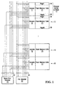
- Figure 1 shows an arrangement of flash memory cells in which there are physical sectors or blocks 10, 12, ..., 14, 16, each with flash memory cells 21, 23, 25, 27 and a respective decoder 11, 13, ..., 15, 17.
- the memory cells of each block are composed of a set of pages (rows).
- Page1 24 and pageN 26 are shown for block 10, and page1 28 and pageN 30 are shown for block 12.
- a block pre-decoder 20 produces a set of block select outputs 32.
- One of the block select outputs and commonly shared signals 32 are connected to each of the blocks.
- a pre-decoder 22 having a set of page select outputs 34.
- the page select outputs 34 are commonly connected to all of the blocks 10, 12, ..., 14, 16.
- block pre-decoder 20 In operation, block pre-decoder 20 generates block select signals 32 to select particular subsets of the blocks 10, 12, 14, 16.
- the pre-decoder 22 generates page select outputs 34 that select particular pages. Once this is done, an erase operation will erase the selected pages from the selected blocks.
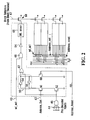
- Figure 2 shows a detailed latch structure to have a multiple page erase function in the core block with a row address decoder.
- the structure of Figure 2 forms part of the decoders 11, 13, ..., 15, 17 of Figure 1 , and is replicated for each page.
- the input wl_act is input as a first input to a NAND gate 48.
- Address_Set 42 is connected to the gate of a transistor 50.
- the pre-decoded inputs X, Y, Z 44 are input to a three input AND gate 45 the output of which is connected to the input of another transistor 52 and to an input of OR gate 62.
- X is connected to receive x or x
- Y is connected to receive y or y
- Z is connected to receive z or z
- x, x , y, y , z and z are outputs of the pre-decoder.
- Each page has a different set of connections to the pre-decoder outputs so that they can be individually selected.
- the decoder circuits for corresponding pages of all of the blocks have the same pre-decoded inputs.
- Address_Reset 46 is connected to the gate of another transistor 60.
- Inverters 54, 56 are connected to form a set-reset (SR) latch 58.
- the output of the set-reset latch 58 is connected to another input of the OR gate 62 the output of which is connected as a second input to the NAND gate 48.
- the output of the NAND gate 48 passes through inverter 64 to WL_driver 66.
- the output of WL_driver 66 passes through block selection transistor 68 that is enabled (or not) by the block selection input 47.
- the block selection input is the same for all the pages of a given block, but is different for each block.
- wl_act 40 needs to be high for any page erase operation.
- Set operation of the set-reset latch 58 is controlled by the Address_set 42 in combination with the output of AND gate 45.
- the output of AND gate 45 is high when the page select signals are appropriately set for that page.
- Both Address_set 42 and the output of AND gate 45 need to be high for a set operation to occur within the set-reset latch 58.
- the reset operation of the set-reset latch 58 is controlled by the Address_reset input 46. When Address_reset is high, a reset occurs.
- the latch 58 is set, the output of OR gate 62 will go high. Assuming wl_act 40 is high, this will produce a high at the output of inverter 64 which goes through the driver 66.
- WL_driver 66 The output of WL_driver 66 will only be connected to the memory cells of that page if the corresponding block selection 47 from the block decoder is also high. WL driver 66 has a low value when erase is needed. 'H' (Vdd level, operating voltage) is non-select, and 'L' (Vss, ground level) is select. The erase voltage is applied to the substrate. (-20v).
- command structure that may be processed by the block decoder and pre-decoder is as follows:
- each page address in a selected block is latched into the latch 58 of each word line decoding block, and multiple word lines to be erased can be selected during the address setting phase prior to when the erase function starts.
- Commonly connected row address decoders in each block are chosen by the pre-decoder and the block decoder.
- the page in the correct block is selected by driving the block selection 47 high on the selected block (to transistor 68 placed between the WL_driver 66 and memory cell blocks (not shown). Because of this, multiple page erase will work properly only if it is limited to erasing multiple pages within the same block.
- Figure 3 shows how a multiple page erase can work properly, when the multiple pages are all within the same block.
- Figure 3 shows a different view of the circuit of Figure 1 .
- the block 10 has been expanded to show word line decoders 80, 82, 84, 86 (forming part of decoder 11 of Figure 1 ) and memory cells 21.
- One of the block select outputs 32 is connected to the respective transistor 68 for each page. Multiple pages being selected will result in the corresponding word line decoders of every block being set. However, if the pages within only the first block 10 are to be erased, then the block select will enable only the first block 10, and as such, only pages within that block will be erased, and that is the desired result.
- the final selection is performed by transistors 68 acting as NMOS switches.
- the WL_drivers for the selected pages in all the blocks generate a page erase voltage (0V). This is only coupled through to the gate level of memory cells of selected blocks because only transistors 68 of selected blocks are switched on. In addition, 20V is applied to the substrate of the flash memory. Because of this reverse voltage between gate (0v) and substrate (20v), the trapped charge of the floating gate of each selected cell can be erased. For unselected cells, WL_driver generates Vdd. The floating level at the vdd applied page line is boosted up by the substrate level (20v) so that the gate of the unselected cell has roughly 16V, and no erase occurs.
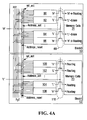
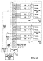
- Figure 4A shows further details of how a multiple page erase can work properly, when the multiple pages are all within the same block.
- Figure 4A shows a different view of the circuit of Figure 1 .
- the block 10 has been expanded as in Figure 3 .
- block 12 has been expanded to show word line decoders 100, 102, 104, 106 (forming part of decoder 13 of Figure 1 ), and memory cells 23.
- the block select output 32 for block 12 is connected to a respective transistor 110 for each page in block 12.
- word line decoders 82, 84 are enabled and therefore produce a "L" output (the erase voltage of the selected cell), and word line decoders 80, 86 are disabled and therefor produce a "H" output. Since pre-decoder outputs are identically connected for every block, corresponding word line decoders for block 12 are enabled and disabled.
- word line decoders 102, 104 are enabled, and word line decoders 100, 106 are disabled.
- block select input is "H" turning on transistors 68, but not turning on transistors 110.
- the result of this is that "L" outputs of the decoders of block 10 are propagated through to the memory cells 21 of block 10, which will be erased when the erase command is asserted.
- the "H” outputs produce a floating state meaning no erase occurs.
- none of the outputs of the decoders 100, 102, 104, 106 are propagated through to memory cells 23, and all of the cells have a floating state meaning no erase occurs, and this is the desired result.
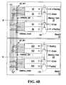
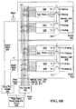
- Figure 4B shows further details of how a multiple page erase can work im properly, when the multiple pages are all within different blocks.
- Figure 4B shows the same circuit details as Figure 4A .
- address information has been generated for the purpose of an erase operation:
- transistors 68 and 110 will all be enabled. Multiple pages being selected will result in the corresponding word line decoders of every block being set. Thus, the outputs of decoders 82, 84, 102, 104 will all be enabled, producing "L" outputs. Since the transistors 68, 110 are all enabled, the erase voltage will be propagated through to the cells 21, 23. The result is that in block0, page1 and page2 are erased AND in block1, page1 and page2 are erased. It is readily apparent that this is more than was to be erased according to the command.
- Figures 5 , 6A and 6B are views of a circuit provided by an embodiment of the invention that provides a page erase functionality. While Figure 5 shows the circuit processing a multiple page erase command with the pages in the same block, Figures 6A and 6B are two views of the same circuit processing a multiple page erase command, with the pages being in different blocks.
- Block 610 has four pages forming part of memory cells 588.
- Block 612 has four pages forming part of memory cells 608. More generally, any number of blocks and pages can be present.
- Block 610 has word line decoders 580, 582, 584, 586 (one per page) connected to memory cells 588 through switching transistors 590.
- Block 612 has word line decoders 600, 602, 604, 606 connected to memory cells 608 through switching transistors 710. Also shown is a block pre-decoder 500.
- the block pre-decoder 500 has a block select output 506 connected to enable/disable switching transistors 590 for block 610, and has a block select output 508 connected to enable/disable switching transistors 710.
- a page pre-decoder 502 is also provided having page select outputs 509 that are commonly connected to corresponding word line decoders in each block as described previously for conventional implementations.
- the page pre-decoder 502 also has an Address_reset output 510 commonly connected to a reset input of each of the word line decoders, an Address_set output 512 commonly connected to a set input of each of the word line decoders, and a WL_act output 514 that is commonly connected to a WL_act input of the word line decoders. Also shown is page select reset generator circuit 504. This circuit has a reset output 516 that is connected to the page pre-decoder 502, or directly to the address reset 510, and to the block pre-decoder 500.
- the connections between the block pre-decoder 500 and the blocks can be considered logical interconnections.
- any function that allows blocks to be individually selected can be implemented. There may be other logic intervening.
- block selection may be performed similar to page selection.
- each block may have a block line decoder that is uniquely addressed by particular bits sent on a set of block select lines.
- the set of block line decoders might be similar to a set of word line decoders of a single block.
- the block line decoders can have a similar reset input for resetting previously latched block addresses.
- the page select reset generator circuit 504 is shown as a separate circuit from the page pre-decoder, but they may be implemented as a single circuit. A specific form of page select outputs is shown, but more generally, any type of page select outputs that allows for corresponding pages of the wordline decoders to be selected may be used. Furthermore, while in some embodiments the wordline decoders of Figures 5 , 6A and 6B are similar in form to the decoders of Figure 2 , more generally, any latching circuits can be employed.
- ATD Address Transition Detect
- DRAM Dynamic Random Access Memory
- SRAM Static Random Access Memory
- FIG. 7 shown is a block sub-address register circuit for latching block addresses forming part of the page select reset generator circuit 504.
- the circuit of Figure 7 has a wr_en input 200 connected to enable inputs of transistors 204, 212.
- the block address input 202 is also connected to the reset input of the latch 210 through inverter 214 and transistor 212.
- the latch 210 has an output that is connected through inverter 216 to produce the overall output 218.
- transistor 204 In operation, when the wr_en input 200 is high, transistor 204 is switched on, and a positive transition on the address input 202 sets the latch 210 consisting of inverters 206, 208. So long as wr_en 200 is high, transistor 212 is also switched on, and a negative transition on the address input 202 will reset the latch 210. The latch state is inverted by inverter 216 to produce the output signal 218, this being the latched block address.
- the circuit of Figure 7 is replicated as many times as the number of block address bits. In this case, from RA ⁇ 16:6>, the block address is 11-bits, and so the circuit of Figure 7 is replicated 11 times.
- Each sub-address register of Figure 7 generates a latched block address output 218 only when enabled by wr_en, and this only occurs when processing page erase addresses. As a result, using such a sub-address register, power consumption by unnecessary address transition detection of other command related row addresses can be avoided.
- FIG. 8 An example of an ATD (Address Transition Detect) circuit is depicted in Figure 8 , but it should be clearly understood that many circuits for implementing an ATD function can be alternatively employed.
- the input 230 is one of the latched block addresses 218 produced by one of the circuits of Figure 7 .
- the circuit of Figure 8 is also replicated as many times as the number of block address bits. In this case, from RA ⁇ 16:6>, the block address is 11-bits, and so the circuit of Figure 8 is replicated 11 times.
- the input 230 is fed to a first input of a first NAND gate 240, through inverter 232 and delay element 236 to a second input of the first NAND gate 240, through inverter 234 to a first input of a second NAND gate 242, and through delay element 238 to a second input of the second NAND gate 242.
- the outputs of the first NAND gate 240 and the second NAND gate 242 are fed to respective inputs of a third NAND gate 244 the output of which is an overall ATD_out signal 246.
- This ATD_out signal is one of the outputs (total 11) that is connected to the input of the ATD merger circuit 340 shown in Figure 9 . More generally, in some embodiments the ATD circuit consists of a first circuit for detecting falling address transitions, a second circuit for detecting rising address transitions, and a circuit for combining the outputs of the first circuit and the second circuit.
- a transition from low to high on the input 230 will result in a pulse (active low) at the output of NAND gate 240 that lasts the duration of the delay introduced by delay element 236. This generates a corresponding pulse (active high) in the ATD_out 246.
- a transition from high to low on the input 230 (falling address transition) will result in a pulse (active low) at the output of NAND gate 242 that lasts the duration of the delay introduced by delay element 238. This generates a corresponding pulse (active high) in the ATD_out 246.
- the circuit will detect any change in the input 230 and generate a pulse in the ATD_out 246 upon such a detection.
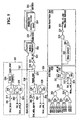
- Figure 9 is a block diagram of an overall circuit for detecting new block addresses. This might for example be implemented as the page reset generator circuit 504 of Figures 5 and 6 .
- Inputs include Row_latch 310, Rst_b 302 (shown input in two places), New_cmd_b 304 (shown input in two places), Radd ⁇ 16:6>, Cmd_addip_pgperse 308.
- Row latch 310 is inverted by inverter 314 and input as a first input to NAND gate 316.
- Rst_b 302 and New_cmd_b are input to NAND gate 318.
- NAND gates 316, 318 are connected as an SR latch 319. The output of the SR latch 319 is input to delay element 330.
- the output 331 of the delay element 330 is labeled Latch_start and this is input to a first input of NAND gate 320.
- Cmd_addip_pgperse 308 is inverted by inverter 324 and input as a first input to NAND gate 326.
- Rst_b 302 and New_cmd_b 304 are input to NAND gate 328.
- NAND gates 326, 328 are connected as an SR latch 329.
- the output 327 of SR latch 329 is labeled Pgpadd_input and this is input to a second input of NAND gate 320.
- NAND gate 320 The output of NAND gate 320 is inverted by inverter 322 to produce wr_en 323 which is input to the sub-address registers 332 described previously with reference to Figure 7 .
- Radd ⁇ 16:6> functions as the input to the address registers 332.
- the output 333 of the address registers 332 is Raddo ⁇ 16:6>, and this is input to the ATD (address transition detect) circuit 334. More specifically, each bit is input to a respective bitwise ATD element, such as shown in Figure 8 .
- These bitwise ATD signals atd ⁇ 16:6> 335 are merged with ATD merger circuit 340.
- a set of bitwise ATD signals are combined with NOR gates 342, 346, 348, 350, NAND gates 352, 354 and NOR gate 356.
- the output of the last NOR gate 356 is latched in SR latch 361 consisting of NAND gates 358, 360.
- the second NAND gate 360 receives Rst_b 302 and New_cmd_b 304.
- the overall merged output atd_all is indicated at 362.
- the atd_all 362 is input to a main reset pulse generator circuit 370. This is input to a first input of NAND gate 364 directly, and to a second input of NAND gate 364 via delay element 366 and inverter 368.
- the output of the NAND gate 364 is inverted by inverter 371 to produce an overall output 372 referred to as dec_rst_pgp (new block address).
- rst_b 302 is asserted (i.e. transitions to low) to initialize the states of all latches and to give a clear known output state to each latch and connected logic.
- new_cmd_b 304 is generated from command assertion. Whenever any new command is asserted, new_cmd_b 304 is asserted (i.e. transitions to low). This also initializes all latches and connected logic. New operation starts each time a new command is asserted.
- cmd_addip_pgperse 308 There is a pulse on the input cmd_addip_pgperse 308 when a command is the address input of a page erase operation. For example, when "address input for page erase" is asserted through an input port of the device, internal clock latches command bits and a command interpreter decodes the 8-bit command. If the decoded result is 'address input for page erase', 'cmd_addip_pgperse' is issued as a pulse from the command interpreter. This pulse is generated and used to start block address detection to determine whether the block address is a same block or a different block. This input is latched by latch 329. When the output Pgpadd_input 327 of latch 329 is high, this means that Row_latch 310 driving Latch_start 331 is in respect of an address input for a page erase operation.
- the 11 bits Radd ⁇ 16:6> 306 are the block address portion of an address, and represent bits of a block address that are used as input values of the sub-address registers described previously. This assumes an implementation with 2048 blocks. More generally, any number can be used. These values are stored in the main address register (not shown) using the timing of the Row_latch pulse.
- the Radd ⁇ 16:6> are latched as a function of the Row_latch 310 as well, and as such there is a delay before the block address appears on Radd ⁇ 16:6>.
- the delay element 330 is provided to obtain Latch_start 331 from the Row_latch input 310.
- the Raddo ⁇ 16:6> output 333 of sub-address registers 332 is then processed by the ATD circuit 334 to produce a respective atd bit per block (atd ⁇ 16:6> 335) and these are combined with the ATD merger circuit 340 to produce atd_all.
- this consists of 11 individual ATD bits merged to produce a single atd_all output 362. If any one or more of atd ⁇ 16:6> is high, then atd_all goes high.
- dec_rst_pgp 372. This is connected to the row address decoders (also referred to as word line decoder(s)) to reset the latch state in case of accessing a different block page.
- the reset signal dec_rst_pgp 372 is issued for the first 'address input for page erase' command, the first page address is decoded and the decoded output is latched into the appropriate word line decoders.
- the reset signal is issued first and then the set signal of the selected decoder latches is issued assuming a change in block address is detected. In the case of consecutive page addresses with the same block address, a further reset signal is not issued. In the case of consecutive page addresses with different block addresses, another reset signal is generated to clear previously latched pages.
- a page select reset enable circuit is provided to enable the generation of the reset output timed properly with the latching of addresses in main address registers.
- the circuitry collectively referred to with reference number 311 fulfils this function, but other circuits can alternatively be employed.
- D flip flops instead of SR latches might be used.
- a page select reset enable circuit is provided to enable the generation of the reset output when the page addresses are in respect of a multi-page erase operation.
- the circuitry collectively referred to with reference number 309 fulfils this function, but other circuits can alternatively be employed.
- D flip flops instead of SR latches might be used.
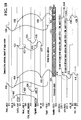
- FIG. 10 shows an example of how the circuit of Figure 9 operates when there are consecutive address inputs for a page erase operation.
- Two cases are shown, one for the case where the two addresses have the same block address, and one for the case where the two addresses have different block addresses.
- the signals are labeled and numbered the same as in Figure 9 .
- a shorthand notation has been employed for atd ⁇ 16:6> in that only a single signal is shown for the atd of a single bit.
- Operation is reset by a pulse 400 on Rst_b 302. This produces a known state on Latch_start 331 and Pgpadd_input 327.
- a start of new command assertion is recognized as signaled by the pulse 402 on New_cmd_b 304. Following this is a pulse 404 on Cmd_Addip_pgperse 308 that indicates that the command is a page erase command. This is latched and produces transition 405 on Pgpadd_input 327.
- the new command input is followed by a pulse 406 on Row_latch 310 indicating that a first row address has been received. This triggers a transition 408 on Latch_start 331.
- the block address for the first address are indicated at 412. Given that this is the first address, the new block address will be different from the unknown state. This is signified by a pulse 414 on atd ⁇ 16:6>, although the pulse would actually occur on one of the 11 atd signals. This is processed by the ATD merger circuit and a pulse 416 is produced on atd_all 362, that in turn generates a main reset pulse 418 on dec_rst_pgp 372. This would reset any latched addresses, but at this point none will have been latched yet. This operation is an initial operation of reset independent of what states there are in the pre-decoder and block-decoder. After the reset operation for the pre-decoder and block pre-decoder, the first received block address and page address are latched as described previously.
- New_cmd_b 304 This resets the Latch_start 331 (negative transition 423) and the Pgpadd_input 327 (negative transition 425) and resets wr_en (negative transition 427).
- a pulse 424 on Cmd_Addip_pgperse 308 that indicates that the command is an address forming part of a page erase command. This is latched and produces transition 429 on Pgpadd_input 327.
- the new command input is followed by a pulse 426 on Row_latch 310 indicating that an address has been received. This triggers a transition 428 on Latch_start 331.
- wr_en 323 triggers the latching of the block addresses Radd ⁇ 16:6> in the sub-address registers 332 as indicated at 431.
- the block address for the second address is indicated at 432. Given that this is the second address, the new block address may or not be different from the previous block address. For the case that the new block address is the same as the previous block address, the resulting atd ⁇ 16:6> is depicted at 335-1. This is short hand notation to indicate there is no transition on any one of the atd ⁇ 16:6> signals. The result is that atd_all is low, and as such there is no main reset pulse. For the case that the new block address is different form the previous block address, the resulting atd ⁇ 16:6> is depicted at 335-2. There is a pulse 434 on atd ⁇ 16:6> this being shorthand notation for the occurrence of a pulse on one of the 11 atd signals.
- a pulse 436 is produced on atd_all 362 that in turn generates a main reset pulse 438 on dec_rst_pgp 372. This will clear the previously latched page address, and the subsequent page address will be latched.
- FIG. 11 this is an example of the operation of the circuit of Figure 9 for sequential commands that are not both page erase commands.
- the example is identical to the example of Figure 10 for the processing of a first command that is a page erase command, and the description of this will not be repeated.
- another new command start is recognized as signaled by the pulse 422 on New_cmd_b 304. This resets the Latch_start 331 (negative transition 423) and the Pgpadd_input 327 (negative transition 425). This in turn resets wr_en 323 (negative transition 427). Following this, there is no Cmd_Addip_pgperse 308 indicating that the command is a page erase command.
- the new command input is followed by a first pulse 450 on Row-latch 310 indicating that an address has been received. This does not trigger any further operation of the circuit because it has not been enabled by the required combination of high states on Latch_start 331 and Pgpadd_input 327.
- the device elements and circuits are connected to each other as shown in the figures, for the sake of simplicity.
- elements, circuits, etc. may be connected directly to each other.
- elements, circuits etc. may be connected indirectly to each other through other elements, circuits, etc., necessary for operation of devices and apparatus.
- the circuit elements and circuits are directly or indirectly coupled with or connected to each other.
- Flash memory More generally, non-volatile memory can be employed.
Description
- The invention relates to page erase functions in flash memories.
- An erase function is used in non-volatile flash memory to restore the original state of a flash cell. Due to physical limitations of the erase operation, it takes a long time to complete the operation. The erase operation takes relatively longer than other main operations such as a page program. For example, where the erase time might be 1.5ms, the page program time might be 25us. With a block erase operation, an entire block is erased at once, a block consisting of a set of pages (rows). Because of this, block erase needs to backup the contents to another memory medium before erasing all contents in the selected block at the same time so as to enable some of the contents (certain pages) to be restored assuming some of the contents of the block should be kept. This requires another memory system to be incorporated in the same board or the same package to support the mentioned data restoration of flash memory. This increases the total system cost with flash memory and makes the data control more complicated.
- Patent Publication
US-A-5784327 discloses an EEPROM operation method wherein erasure is performed on one or more pages in a non-volatile from memory and wherein registers after each page- or block erasure are reset. - According to one broad aspect, the invention provides a page select reset generator circuit for limiting multi-page erase operations in non-volatile memory, the page select reset generator circuit comprising: an input for receiving block address portions of each address of a set of one or more addresses; an address transition detect circuit that detects when block address portions of two addresses of the set of page addresses are different; the page select reset generator being operable to generate a reset output for clearing latched pages upon detecting that block address portions of two addresses are different.
- In some embodiments, the page select reset generator circuit is for limiting multi-page erase operations in non-volatile memory comprising flash memory.
- In some embodiments, the page select reset generator circuit further comprises: a first page select reset enable circuit that enables the generation of the reset output when the addresses are in respect of multi-page erase operation.
- In some embodiments, the page select reset generator circuit further comprises: a second page select reset enable circuit that enables the generation of the reset output timed properly with the latching of addresses in main address registers.
- In some embodiments, the page select reset generator circuit further comprises: a first page select reset enable circuit that enables the generation of the reset output when the page addresses are in respect of multi-page erase operation; a second page select reset enable circuit that enables the generation of the reset output timed properly with the latching of addresses in main address registers; wherein the page select reset generator is operable to generate the reset output only when enabled by both the first page select reset enable circuit and the second page select reset enable circuit.
- In some embodiments, the address transition detect circuit comprises: for each bit of a multi-bit block address: a) a respective sub-address register for registering the bit and producing a registered address output; b) a respective bitwise address detection circuit for detecting a transition in the registered address output; a merger circuit for combining outputs of the bitwise address detection circuits.
- In some embodiments, each bitwise address detection circuit comprises: a first circuit for detecting rising address transitions; a second circuit for detecting falling address transitions; a circuit for combining outputs of the first circuit and the second circuit.
- In some embodiments, the first circuit for detecting rising address transitions comprises: a) an inverter and a delay element connected together in sequence; b) a NAND gate having a first input connected to receive one of the registered address outputs, the NAND gate having a second input connected to receive the one of the registered address outputs after inversion by the inverter and delay by the delay element; the second circuit for detecting falling address transitions comprises: a) an inverter and a delay element; b) a NAND gate having a first input connected to receive one of the registered address outputs after inversion by the inverter, the NAND gate having a second input connected to receive the one of the registered address outputs after delay by the delay element.
- In some embodiments, for each bit of the multi-bit block address, the respective sub-address register comprises: an SR latch having an input connected to receive the bit; an enable circuit for enabling latching of the bit to the SR latch that enables the generation of the reset output when the page addresses are in respect of multi-page erase operation.
- In some embodiments, the page select reset generator circuit further comprises: a main reset pulse generator circuit.
- According to another broad aspect, the invention provides a memory circuit comprising: a plurality of memory blocks, each block comprising non-volatile memory cells arranged in a plurality of pages; a respective latching circuit for each page, each page having a page address, the page addresses of the pages being unique within each block, the page address of each page being the same as that of a corresponding page in each other block; a respective block enable circuit for each block; a block pre-decoder circuit that processes a block address portion of each address of a page erase command by enabling the block enable circuit for the block identified by the block address portion of the address; a page pre-decoder circuit that processes a page address portion of each address of a page erase command by setting the latching circuit for each page having the page address identified by the address portion; the page select reset generator circuit as summarized above; the latching circuits being further operable to connect an erase voltage to the selected pages of the enabled blocks after all addresses of the page erase command have been processed by the block pre-decoder, the page pre-decoder, and the page select reset generator circuit; wherein accidental erasure of pages due to a multi-page erase operation relating to two or more different block addresses is prevented.
- In some embodiments, the non-volatile memory comprises flash memory.
- In some embodiments, the latching circuits have a commonly connected reset input for receiving the reset output generated by the page select reset generator.
- According to another broad aspect, the invention provides a method comprising: for each of a plurality of addresses of a multi-page erase operation pertaining to a non-volatile memory, each address containing a block address portion and a page address portion: a) detecting whether the block address portion differs from that of a previous address of the plurality of addresses; b) resetting any previous selections of pages and blocks upon detecting that the block address differs from that of a previous address of the plurality of addresses; c) selecting a respective page in each of a plurality of blocks; d) selecting a respective one of the plurality of blocks; and wherein after said detecting, resetting, selecting a respective page and selecting a respective one of the plurality of blocks on each address, a single remaining block address will be selected, the method further comprising erasing any selected pages in the single remaining selected block.
- In some embodiments, the method further comprises: generating a reset output to reset the previous selections.
- In some embodiments, the method further comprises: receiving addresses, each address containing a block address portion and a page address portion; for each received address, determining if the address is part of a page erase operation; performing said detecting and resetting only if the address is determined to be part of a page erase operation.
- In some embodiments, the method further comprises; latching addresses in main address registers; timing the generation of the reset output with the latching of addresses in main address registers.
- In some embodiments, detecting whether the block address portion differs from that of a previous address of the plurality of addresses comprises: for each bit of a multi-bit block address: a) registering the bit into a respective sub-address register; b) performing bitwise address detection to detect a transition in an output of the sub-address register; combining outputs of the bitwise address detection.
- In some embodiments, performing bitwise address detection comprises: detecting rising address transitions; and detecting falling address transitions.
- In some embodiments, the method is applied to flash memory.
- Embodiments of the present invention will now be described, by way of example only, with reference to the attached figures, wherein:
-
Figure 1 is a schematic diagram of a flash memory system; -
Figure 2 is a circuit diagram of a decoder circuit for flash memory cells; -
Figure 3 is a circuit diagram of a flash memory system showing more detail of the block decoder connections; -
Figure 4A is a circuit diagram of a flash memory system showing the behaviour when performing a multiple page erase within a single block; -
Figure 4B is a circuit diagram of a flash memory system showing the behaviour when a multiple page erase operation is performed with pages in different blocks; -
Figure 5 is a schematic diagram of a flash memory system showing correct behaviour for multiple pages being erased within a single block; -
Figures 6A and6B show schematic diagrams of a flash memory system showing a multiple page erase in multiple blocks being attempted, but with page addresses being reset upon detection of a different block; -
Figure 7 is a detailed circuit diagram of a sub-address register; -
Figure 8 is a detailed circuit diagram of an ATD (Address Transition Detect) circuit; -
Figure 9 is a detailed circuit diagram of a circuit that detects when there has been a block address change during a multiple page erase operation, and generates a reset pulse accordingly to reset the page addresses; -
Figure 10 is a first example of the operation of the circuit ofFigure 9 for consecutive address inputs of a page erase operation; and -
Figure 11 is a second example of the operation of the circuit ofFigure 9 for consecutive commands that are not both page addresses. - Because of the limitations of block erase, page based erase has been introduced as an alternative of block erase operation in flash memories. Examples are described in Applicant's co-pending United States Provisional Patent Applications Serial No.
60/786,897 filed March 29, 2006 60/843,593 filed on September 11, 2006 -
Figure 1 shows an arrangement of flash memory cells in which there are physical sectors orblocks flash memory cells respective decoder Page1 24 andpageN 26 are shown forblock 10, andpage1 28 andpageN 30 are shown forblock 12. A block pre-decoder 20 produces a set of blockselect outputs 32. One of the block select outputs and commonly sharedsignals 32 are connected to each of the blocks. There is also shown a pre-decoder 22 having a set of page selectoutputs 34. The pageselect outputs 34 are commonly connected to all of theblocks pre-decoder 20 generates blockselect signals 32 to select particular subsets of theblocks select outputs 34 that select particular pages. Once this is done, an erase operation will erase the selected pages from the selected blocks. -
Figure 2 shows a detailed latch structure to have a multiple page erase function in the core block with a row address decoder. The structure ofFigure 2 forms part of thedecoders Figure 1 , and is replicated for each page. The circuit has inputs consisting of wl_act (wordline active = pageline active) 40,Address_Set 42, pre-decoded inputs X, Y, Z 44 (outputs ofpre-decoder 22 ofFigure 1 ),Address_Reset 46, and block selection 47 (one of the block selection signals 32 fromblock decoder 20 ofFigure 1 ). The input wl_act is input as a first input to aNAND gate 48.Address_Set 42 is connected to the gate of atransistor 50. The pre-decoded inputs X, Y,Z 44 are input to a three input ANDgate 45 the output of which is connected to the input of anothertransistor 52 and to an input ofOR gate 62. For this example, for a given page, X is connected to receive x orx , Y is connected to receive y ory , and Z is connected to receive z orz , where x,x , y,y , z andz are outputs of the pre-decoder. Each page has a different set of connections to the pre-decoder outputs so that they can be individually selected. The decoder circuits for corresponding pages of all of the blocks have the same pre-decoded inputs.Address_Reset 46 is connected to the gate of anothertransistor 60.Inverters latch 58. The output of the set-reset latch 58 is connected to another input of theOR gate 62 the output of which is connected as a second input to theNAND gate 48. The output of theNAND gate 48 passes throughinverter 64 toWL_driver 66. The output ofWL_driver 66 passes throughblock selection transistor 68 that is enabled (or not) by theblock selection input 47. The block selection input is the same for all the pages of a given block, but is different for each block. - In operation, wl_act 40 needs to be high for any page erase operation. Set operation of the set-
reset latch 58 is controlled by theAddress_set 42 in combination with the output of ANDgate 45. The output of ANDgate 45 is high when the page select signals are appropriately set for that page. BothAddress_set 42 and the output of ANDgate 45 need to be high for a set operation to occur within the set-reset latch 58. The reset operation of the set-reset latch 58 is controlled by theAddress_reset input 46. When Address_reset is high, a reset occurs. When thelatch 58 is set, the output ofOR gate 62 will go high. Assumingwl_act 40 is high, this will produce a high at the output ofinverter 64 which goes through thedriver 66. The output ofWL_driver 66 will only be connected to the memory cells of that page if thecorresponding block selection 47 from the block decoder is also high.WL driver 66 has a low value when erase is needed. 'H' (Vdd level, operating voltage) is non-select, and 'L' (Vss, ground level) is select. The erase voltage is applied to the substrate. (-20v). - An example of a command structure that may be processed by the block decoder and pre-decoder is as follows:
- {block B1, page P1}, {block B2, page P2}, ...,{block BK, page PK}, erase
- The circuit of
Figure 2 is repeated for each page. With this structure, each page address in a selected block is latched into thelatch 58 of each word line decoding block, and multiple word lines to be erased can be selected during the address setting phase prior to when the erase function starts. Commonly connected row address decoders in each block, at the same time, are chosen by the pre-decoder and the block decoder. The page in the correct block is selected by driving theblock selection 47 high on the selected block (totransistor 68 placed between theWL_driver 66 and memory cell blocks (not shown). Because of this, multiple page erase will work properly only if it is limited to erasing multiple pages within the same block. -
Figure 3 shows how a multiple page erase can work properly, when the multiple pages are all within the same block.Figure 3 shows a different view of the circuit ofFigure 1 . Theblock 10 has been expanded to show word line decoders 80, 82, 84, 86 (forming part ofdecoder 11 ofFigure 1 ) andmemory cells 21. One of the blockselect outputs 32 is connected to therespective transistor 68 for each page. Multiple pages being selected will result in the corresponding word line decoders of every block being set. However, if the pages within only thefirst block 10 are to be erased, then the block select will enable only thefirst block 10, and as such, only pages within that block will be erased, and that is the desired result. The final selection is performed bytransistors 68 acting as NMOS switches. The WL_drivers for the selected pages in all the blocks generate a page erase voltage (0V). This is only coupled through to the gate level of memory cells of selected blocks becauseonly transistors 68 of selected blocks are switched on. In addition, 20V is applied to the substrate of the flash memory. Because of this reverse voltage between gate (0v) and substrate (20v), the trapped charge of the floating gate of each selected cell can be erased. For unselected cells, WL_driver generates Vdd. The floating level at the vdd applied page line is boosted up by the substrate level (20v) so that the gate of the unselected cell has roughly 16V, and no erase occurs. -
Figure 4A shows further details of how a multiple page erase can work properly, when the multiple pages are all within the same block.Figure 4A shows a different view of the circuit ofFigure 1 . Theblock 10 has been expanded as inFigure 3 . In addition, block 12 has been expanded to showword line decoders decoder 13 ofFigure 1 ), andmemory cells 23. The blockselect output 32 forblock 12 is connected to arespective transistor 110 for each page inblock 12. For the purpose of this example, it is assumed that the following address information has been generated for the purpose of an erase operation where it is assumed block0 isblock 10, block1 isblock 12, page0 is the page associated withdecoders decoders decoders decoders 86, 106: - {block0, page1}, {block0, page2}, erase
- Multiple pages being selected will result in the corresponding word line decoders of every block being set. However, if pages within the same block are to be erased (block0 in this example), then the block select will enable only the
first block 10, and as such, only pages within that block will be erased, and that is the desired result. Here it is assumed that word line decoders 82, 84 are enabled and therefore produce a "L" output (the erase voltage of the selected cell), and word line decoders 80, 86 are disabled and therefor produce a "H" output. Since pre-decoder outputs are identically connected for every block, corresponding word line decoders forblock 12 are enabled and disabled. More specifically,word line decoders word line decoders transistors 68, but not turning ontransistors 110. The result of this is that "L" outputs of the decoders ofblock 10 are propagated through to thememory cells 21 ofblock 10, which will be erased when the erase command is asserted. The "H" outputs produce a floating state meaning no erase occurs. Inblock 12, none of the outputs of thedecoders memory cells 23, and all of the cells have a floating state meaning no erase occurs, and this is the desired result. -
Figure 4B shows further details of how a multiple page erase can work im properly, when the multiple pages are all within different blocks.Figure 4B shows the same circuit details asFigure 4A . For the purpose of this example, it is assumed that the following address information has been generated for the purpose of an erase operation: - {block0, page1}, {block1, page2}, erase
- Since both blocks are selected,
transistors decoders transistors cells -
Figures 5 ,6A and6B are views of a circuit provided by an embodiment of the invention that provides a page erase functionality. WhileFigure 5 shows the circuit processing a multiple page erase command with the pages in the same block,Figures 6A and6B are two views of the same circuit processing a multiple page erase command, with the pages being in different blocks. In the circuits, there are twoblocks Block 610 has four pages forming part ofmemory cells 588.Block 612 has four pages forming part ofmemory cells 608. More generally, any number of blocks and pages can be present.Block 610 hasword line decoders memory cells 588 through switchingtransistors 590.Block 612 hasword line decoders memory cells 608 through switchingtransistors 710. Also shown is ablock pre-decoder 500. Theblock pre-decoder 500 has a blockselect output 506 connected to enable/disable switchingtransistors 590 forblock 610, and has a blockselect output 508 connected to enable/disable switchingtransistors 710. Apage pre-decoder 502 is also provided having pageselect outputs 509 that are commonly connected to corresponding word line decoders in each block as described previously for conventional implementations. Thepage pre-decoder 502 also has anAddress_reset output 510 commonly connected to a reset input of each of the word line decoders, anAddress_set output 512 commonly connected to a set input of each of the word line decoders, and aWL_act output 514 that is commonly connected to a WL_act input of the word line decoders. Also shown is page selectreset generator circuit 504. This circuit has areset output 516 that is connected to thepage pre-decoder 502, or directly to the address reset 510, and to theblock pre-decoder 500. - In
Figures 5 ,6A and6B , the connections between theblock pre-decoder 500 and the blocks can be considered logical interconnections. Generally, any function that allows blocks to be individually selected can be implemented. There may be other logic intervening. For example, for implementations with a large number of blocks (such as 2048 in the example below), block selection may be performed similar to page selection. For example, each block may have a block line decoder that is uniquely addressed by particular bits sent on a set of block select lines. In other words, the set of block line decoders might be similar to a set of word line decoders of a single block. The block line decoders can have a similar reset input for resetting previously latched block addresses. - The page select
reset generator circuit 504 is shown as a separate circuit from the page pre-decoder, but they may be implemented as a single circuit. A specific form of page select outputs is shown, but more generally, any type of page select outputs that allows for corresponding pages of the wordline decoders to be selected may be used. Furthermore, while in some embodiments the wordline decoders ofFigures 5 ,6A and6B are similar in form to the decoders ofFigure 2 , more generally, any latching circuits can be employed. - In operation, multiple pages being selected will result in the corresponding word line decoders of every block being set. Assuming the pages are in the same block, the page select
reset generator circuit 504 will not generate a reset. After all the addresses have been set, the erase operation is executed, and the erase voltage (0v) will be propagated to the pages of the selected block through the appropriate control of switching transistors (by turning ontransistors 590 forblock 610, or by turning ontransistors 710 for block 612). On the other hand, when the pages are not in the same block, as soon as a different block is detected, the page selectreset generator circuit 504 produces a reset onreset output 516 that resets all previously set page addresses and resets block addresses. Subsequent addresses are latched and erased normally assuming they all belong to the same block. - In
Figure 5 , an example of a multiple page erase operation in the same block is shown. Here the operation contemplated is: - {Block0, page1}, {Block0, page2} erase
- At the instants depicted in
Figures 6A and6B , shown are sequential states of the circuit for an example of a multiple page erase operation for page addresses in different blocks. Here the operation contemplated is: - {Block0, page1}, {Block1, page2} erase
- Details of example implementations of the page select
reset generator circuit 504 will now be provided. In some embodiments, in order to implement the described operations, different block address detection is performed using an ATD (Address Transition Detect) mechanism. It is noted that ATD (address transition detect) has been popularly used in asynchronous DRAM (Dynamic Random Access Memory) and SRAM (Static Random Access Memory) to find the start of a new address. As a function of detected address changes, internal control logic generates the relevant signals in DRAM or SRAM. The pulse width and multiple or single address transitions were critical factors when circuit design of asynchronous DRAM or SRAM was considered and because of this, complicated logic was used to perform the ATD function. - Referring now to
Figure 7 , shown is a block sub-address register circuit for latching block addresses forming part of the page selectreset generator circuit 504. The circuit ofFigure 7 has awr_en input 200 connected to enable inputs oftransistors block address input 202 that is connected to the set input of alatch 210 consisting ofinverters transistor 204. Theblock address input 202 is also connected to the reset input of thelatch 210 throughinverter 214 andtransistor 212. Thelatch 210 has an output that is connected throughinverter 216 to produce theoverall output 218. - In operation, when the
wr_en input 200 is high,transistor 204 is switched on, and a positive transition on theaddress input 202 sets thelatch 210 consisting ofinverters wr_en 200 is high,transistor 212 is also switched on, and a negative transition on theaddress input 202 will reset thelatch 210. The latch state is inverted byinverter 216 to produce theoutput signal 218, this being the latched block address. The circuit ofFigure 7 is replicated as many times as the number of block address bits. In this case, from RA<16:6>, the block address is 11-bits, and so the circuit ofFigure 7 is replicated 11 times. After storing row addresses in the main address registers consisting of block addresses and page addresses (not shown), block addresses are latched into the sub-address register ofFigure 7 . The 'wr_en'control signal 200 is generated from a two input combination. The first input, cmd_addip_pgperse signifies that the most recent command is a page erase address input command, and the second input is a Row-latch used in the main address registers placed in register blocks prior to theFigure 7 sub-address register (not shown). A specific mechanism of combining cmd_addip_pgperse and Row-latch will be detailed below in the description ofFigure 9 . - Each sub-address register of
Figure 7 generates a latchedblock address output 218 only when enabled by wr_en, and this only occurs when processing page erase addresses. As a result, using such a sub-address register, power consumption by unnecessary address transition detection of other command related row addresses can be avoided. - An example of an ATD (Address Transition Detect) circuit is depicted in
Figure 8 , but it should be clearly understood that many circuits for implementing an ATD function can be alternatively employed. InFigure 8 , theinput 230 is one of the latched block addresses 218 produced by one of the circuits ofFigure 7 . The circuit ofFigure 8 is also replicated as many times as the number of block address bits. In this case, from RA<16:6>, the block address is 11-bits, and so the circuit ofFigure 8 is replicated 11 times. Theinput 230 is fed to a first input of afirst NAND gate 240, throughinverter 232 anddelay element 236 to a second input of thefirst NAND gate 240, throughinverter 234 to a first input of asecond NAND gate 242, and throughdelay element 238 to a second input of thesecond NAND gate 242. The outputs of thefirst NAND gate 240 and thesecond NAND gate 242 are fed to respective inputs of athird NAND gate 244 the output of which is an overallATD_out signal 246. This ATD_out signal is one of the outputs (total 11) that is connected to the input of theATD merger circuit 340 shown inFigure 9 . More generally, in some embodiments the ATD circuit consists of a first circuit for detecting falling address transitions, a second circuit for detecting rising address transitions, and a circuit for combining the outputs of the first circuit and the second circuit. - In operation, a transition from low to high on the input 230 (rising address transition) will result in a pulse (active low) at the output of
NAND gate 240 that lasts the duration of the delay introduced bydelay element 236. This generates a corresponding pulse (active high) in theATD_out 246. A transition from high to low on the input 230 (falling address transition) will result in a pulse (active low) at the output ofNAND gate 242 that lasts the duration of the delay introduced bydelay element 238. This generates a corresponding pulse (active high) in theATD_out 246. Thus, the circuit will detect any change in theinput 230 and generate a pulse in theATD_out 246 upon such a detection. -
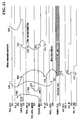
Figure 9 is a block diagram of an overall circuit for detecting new block addresses. This might for example be implemented as the pagereset generator circuit 504 ofFigures 5 and6 . Inputs includeRow_latch 310, Rst_b 302 (shown input in two places), New_cmd_b 304 (shown input in two places), Radd<16:6>,Cmd_addip_pgperse 308.Row latch 310 is inverted byinverter 314 and input as a first input toNAND gate 316.Rst_b 302 and New_cmd_b are input toNAND gate 318.NAND gates SR latch 319. The output of theSR latch 319 is input to delayelement 330. Theoutput 331 of thedelay element 330 is labeled Latch_start and this is input to a first input ofNAND gate 320. Similarly,Cmd_addip_pgperse 308 is inverted byinverter 324 and input as a first input toNAND gate 326.Rst_b 302 andNew_cmd_b 304 are input toNAND gate 328.NAND gates SR latch 329. Theoutput 327 ofSR latch 329 is labeled Pgpadd_input and this is input to a second input ofNAND gate 320. The output ofNAND gate 320 is inverted byinverter 322 to produce wr_en 323 which is input to thesub-address registers 332 described previously with reference toFigure 7 . Radd<16:6> functions as the input to the address registers 332. Theoutput 333 of the address registers 332 is Raddo<16:6>, and this is input to the ATD (address transition detect)circuit 334. More specifically, each bit is input to a respective bitwise ATD element, such as shown inFigure 8 . These bitwise ATD signals atd<16:6> 335 are merged withATD merger circuit 340. A set of bitwise ATD signals are combined with NORgates NAND gates gate 356. The output of the last NORgate 356 is latched inSR latch 361 consisting ofNAND gates second NAND gate 360 receivesRst_b 302 andNew_cmd_b 304. The overall merged output atd_all is indicated at 362. Theatd_all 362 is input to a main resetpulse generator circuit 370. This is input to a first input ofNAND gate 364 directly, and to a second input ofNAND gate 364 viadelay element 366 andinverter 368. The output of theNAND gate 364 is inverted byinverter 371 to produce anoverall output 372 referred to as dec_rst_pgp (new block address). - The operation of the circuit of
Figure 9 will be described now in detail. Before the start of normal operation,rst_b 302 is asserted (i.e. transitions to low) to initialize the states of all latches and to give a clear known output state to each latch and connected logic. - The
signal new_cmd_b 304 is generated from command assertion. Whenever any new command is asserted,new_cmd_b 304 is asserted (i.e. transitions to low). This also initializes all latches and connected logic. New operation starts each time a new command is asserted. - There is a pulse on the input cmd_addip_pgperse 308 when a command is the address input of a page erase operation. For example, when "address input for page erase" is asserted through an input port of the device, internal clock latches command bits and a command interpreter decodes the 8-bit command. If the decoded result is 'address input for page erase', 'cmd_addip_pgperse' is issued as a pulse from the command interpreter. This pulse is generated and used to start block address detection to determine whether the block address is a same block or a different block. This input is latched by
latch 329. When theoutput Pgpadd_input 327 oflatch 329 is high, this means thatRow_latch 310 drivingLatch_start 331 is in respect of an address input for a page erase operation. - When an address input of page erase is asserted
Pgpadd_input 327 goes high, andRow_latch 310 is generated soLatch_start 331 goes high, and then wr_en 323 (output of inverter 322) goes to high and is reset by anew_cmd_b 304 orrst_b 302. This enables the start of block address transition detection. - The 11 bits Radd<16:6> 306 are the block address portion of an address, and represent bits of a block address that are used as input values of the sub-address registers described previously. This assumes an implementation with 2048 blocks. More generally, any number can be used. These values are stored in the main address register (not shown) using the timing of the Row_latch pulse. In some embodiments, the Radd<16:6> are latched as a function of the
Row_latch 310 as well, and as such there is a delay before the block address appears on Radd<16:6>. In order to get the timing margin between Radd<16:6> 306 andwr_en 323, thedelay element 330 is provided to obtainLatch_start 331 from theRow_latch input 310. - The Raddo<16:6>
output 333 ofsub-address registers 332 is then processed by theATD circuit 334 to produce a respective atd bit per block (atd<16:6> 335) and these are combined with theATD merger circuit 340 to produce atd_all. In the illustrated example, this consists of 11 individual ATD bits merged to produce asingle atd_all output 362. If any one or more of atd<16:6> is high, then atd_all goes high. - When atd_all 362 goes high, the final output is a pulse on
dec_rst_pgp 372. This is connected to the row address decoders (also referred to as word line decoder(s)) to reset the latch state in case of accessing a different block page. - Once the
reset signal dec_rst_pgp 372 is issued for the first 'address input for page erase' command, the first page address is decoded and the decoded output is latched into the appropriate word line decoders. The reset signal is issued first and then the set signal of the selected decoder latches is issued assuming a change in block address is detected. In the case of consecutive page addresses with the same block address, a further reset signal is not issued. In the case of consecutive page addresses with different block addresses, another reset signal is generated to clear previously latched pages. - In some embodiments a page select reset enable circuit is provided to enable the generation of the reset output timed properly with the latching of addresses in main address registers. For the example of
Figure 9 , the circuitry collectively referred to withreference number 311 fulfils this function, but other circuits can alternatively be employed. For example D flip flops instead of SR latches might be used. - In some embodiments a page select reset enable circuit is provided to enable the generation of the reset output when the page addresses are in respect of a multi-page erase operation. For the example of
Figure 9 , the circuitry collectively referred to withreference number 309 fulfils this function, but other circuits can alternatively be employed. For example D flip flops instead of SR latches might be used. - To further assist in the understanding of the circuit of
Figure 9 , two specific operational examples will now be described with reference toFigures 10 and11 . Referring first toFigure 10 , this shows an example of how the circuit ofFigure 9 operates when there are consecutive address inputs for a page erase operation. Two cases are shown, one for the case where the two addresses have the same block address, and one for the case where the two addresses have different block addresses. The signals are labeled and numbered the same as inFigure 9 . A shorthand notation has been employed for atd<16:6> in that only a single signal is shown for the atd of a single bit. - Operation is reset by a
pulse 400 onRst_b 302. This produces a known state onLatch_start 331 andPgpadd_input 327. A start of new command assertion is recognized as signaled by thepulse 402 onNew_cmd_b 304. Following this is apulse 404 onCmd_Addip_pgperse 308 that indicates that the command is a page erase command. This is latched and producestransition 405 onPgpadd_input 327. The new command input is followed by apulse 406 onRow_latch 310 indicating that a first row address has been received. This triggers atransition 408 onLatch_start 331. The combination of high states onLatch_start 331 andPgpadd_input 327 result in atransition 410 onwr_en 323. In turn, wr_en 323 triggers the latching of the block addresses Radd<16:6> in thesub-address registers 332 at 411. - The block address for the first address are indicated at 412. Given that this is the first address, the new block address will be different from the unknown state. This is signified by a
pulse 414 on atd<16:6>, although the pulse would actually occur on one of the 11 atd signals. This is processed by the ATD merger circuit and apulse 416 is produced onatd_all 362, that in turn generates amain reset pulse 418 ondec_rst_pgp 372. This would reset any latched addresses, but at this point none will have been latched yet. This operation is an initial operation of reset independent of what states there are in the pre-decoder and block-decoder. After the reset operation for the pre-decoder and block pre-decoder, the first received block address and page address are latched as described previously. - Some time later, another new command is received as signaled by the
pulse 422 onNew_cmd_b 304. This resets the Latch_start 331 (negative transition 423) and the Pgpadd_input 327 (negative transition 425) and resets wr_en (negative transition 427). Following this is apulse 424 onCmd_Addip_pgperse 308 that indicates that the command is an address forming part of a page erase command. This is latched and producestransition 429 onPgpadd_input 327. The new command input is followed by apulse 426 onRow_latch 310 indicating that an address has been received. This triggers atransition 428 onLatch_start 331. The combination of high states onLatch_start 331 andPgpadd_input 327 result in atransition 430 onwr_en 323. In turn, wr_en 323 triggers the latching of the block addresses Radd<16:6> in thesub-address registers 332 as indicated at 431. - The block address for the second address is indicated at 432. Given that this is the second address, the new block address may or not be different from the previous block address. For the case that the new block address is the same as the previous block address, the resulting atd<16:6> is depicted at 335-1. This is short hand notation to indicate there is no transition on any one of the atd<16:6> signals. The result is that atd_all is low, and as such there is no main reset pulse. For the case that the new block address is different form the previous block address, the resulting atd<16:6> is depicted at 335-2. There is a
pulse 434 on atd<16:6> this being shorthand notation for the occurrence of a pulse on one of the 11 atd signals. This is processed by the ATD merger circuit and apulse 436 is produced onatd_all 362 that in turn generates amain reset pulse 438 ondec_rst_pgp 372. This will clear the previously latched page address, and the subsequent page address will be latched. - Turning now to
Figure 11 , this is an example of the operation of the circuit ofFigure 9 for sequential commands that are not both page erase commands. The example is identical to the example ofFigure 10 for the processing of a first command that is a page erase command, and the description of this will not be repeated. Some time later, another new command start is recognized as signaled by thepulse 422 onNew_cmd_b 304. This resets the Latch_start 331 (negative transition 423) and the Pgpadd_input 327 (negative transition 425). This in turn resets wr_en 323 (negative transition 427). Following this, there is noCmd_Addip_pgperse 308 indicating that the command is a page erase command. The new command input is followed by afirst pulse 450 on Row-latch 310 indicating that an address has been received. This does not trigger any further operation of the circuit because it has not been enabled by the required combination of high states onLatch_start 331 andPgpadd_input 327. - In the embodiments described above, the device elements and circuits are connected to each other as shown in the figures, for the sake of simplicity. In practical applications of the present invention, elements, circuits, etc. may be connected directly to each other. As well, elements, circuits etc. may be connected indirectly to each other through other elements, circuits, etc., necessary for operation of devices and apparatus. Thus, in actual configuration, the circuit elements and circuits are directly or indirectly coupled with or connected to each other.
- The embodiments above have assumed the use of Flash memory. More generally, non-volatile memory can be employed.
- The above-described embodiments of the present invention are intended to be examples only. Alterations, modifications and variations may be effected to the particular embodiments by those of skill in the art without departing from the scope of the invention, which is defined solely by the claims appended hereto.
Claims (15)
- A non-volatile memory comprising memory blocks (10, 12, 14, 16), each memory block comprising:non-volatile memory cells arranged in a plurality of pages (24, 26, 28, 30), each page having a page address (X, Y, Z), the page addresses of the pages being unique within each block, the page address of each page being the same as that of a corresponding page in each other block:characterized by:a respective latching circuit (58) for each page operable to connect an erase voltage to the page to be erased responsive to a page address; anda page select reset generator (504, Figs. 7, 8, 9) configured to limit a multi-page erase operation to a single selected memory block in said non-volatile memory, the page select reset generator circuit comprising:an input configured to receive memory block address portions (306) of each address of a set of one or more addresses of pages to be erased:an address transition detect circuit (334) configured to detect when memory block address portions of two addresses of the set of page addresses are different;the page select reset generator being operable to generate a reset output (516, 372) to limit erasing of multiple pages to pages within the same block by clearing latching circuits upon detecting that block address portions of two addresses are different.
- The non-volatile memory of claim 1 wherein the non-volatile memory is a flash memory.
- The non-volatile memory of claim 1 wherein the page select reset generator further comprises:a first page select reset enable circuit (309) configured to enable the generation of the reset output when the addresses are in respect of multi-page erase operation;a second page select reset enable circuit (311) configured to enable the generation of the reset output timed properly with the latching of addresses in main address registers; ora first page select reset enable circuit (309) configured to enable the generation of the reset output when the page addresses are in respect of multi-page erase operation, and a second page select reset enable circuit (311) that enables the generation of the reset output timed properly with the latching of addresses in main address registers, the page select reset generator being operable to generate the reset output only when enabled by both the first page select reset enable circuit and the second page select reset enable circuit.
- The non-volatile memory of claim 1 wherein the address transition detect circuit comprises:for each bit of a multi-bit block address:a) a respective sub-address register (332) that registers the bit and produces a registered address output;b) a respective bitwise address transition detection circuit (334) that detects a transition in the registered address output;a merger circuit (340) that combines outputs of the bitwise address transition detection circuits.
- The non-volatile memory of claim 4 wherein each bitwise address transition detection circuit comprises:a first circuit (232, 236, 240) that detects rising address transitions;a second circuit (234, 238, 242) that detects falling address transitions;a circuit (244) that combines outputs of the first circuit and the second circuit.
- The non-volatile memory of claim 5 wherein:the first circuit for detecting rising address transitions comprises:a) an inverter (232) and a delay element (236) connected together in sequence;b) a NAND gate (240) having a first input connected to receive one of the registered address outputs, the NAND gate having a second input connected to receive the one of the registered address outputs after inversion by the inverter and delay by the delay element; andthe second circuit for detecting falling address transitions comprises:a) an inverter (234) and a delay element (238);b) a NAND gate (242) having a first input connected to receive one of the registered address outputs after inversion by the inverter, the NAND gate having a second input connected to receive the one of the registered address outputs after delay by the delay element.
- The non-volatile memory of claim 4 wherein for each bit of the multi-bit block address, the respective sub-address register comprises:a Set/Reset (SR) latch (210) having an input connected to receive the bit;an enable circuit (204, 212) that enables latching of the bit to the SR latch that enables the generation of the reset output when the page addresses are in respect of the multi-page erase operation.
- The non-volatile memory of claim 5 further comprising:a main reset pulse generator circuit (370).
- The non-volatile memory of claim 1 further comprising:a respective block enable circuit (590, 710) for each block;a block pre-decoder circuit (500) that processes a block address portion of each address of a page erase command by enabling the block enable circuit for the block identified by the block address portion of the address; anda page pre-decoder circuit (502) that processes a page address portion of each address of a page erase command by setting the latching circuit for each page having the page address identified by the address portion;the latching circuits being further operable to connect an erase voltage to the selected pages of the enabled blocks after all addresses of the page erase command have been processed by the block pre-decoder, the page pre-decoder, and the page select reset generator circuit;wherein accidental erasure of pages due to a multi-page erase operation relating to two or more different block addresses is prevented.
- The non-volatile memory of claim 9 wherein:the latching circuits have a commonly connected reset input for receiving the reset output generated by the page select reset generator.
- A method of erasing pages in a non-volatile memory comprising memory blocks (10, 12, 14, 16), each memory block comprising:non-volatile memory cells arranged in a plurality of pages (24, 26, 28, 30), each page having a page address (X, Y, Z), the page addresses of the pages being unique within each block, the page address of each page being the same as that of a corresponding page in each other block:characterized by:for each of a plurality of addresses of a multi-page erase operation pertaining to the non-volatile memory, each address containing a block address portion and a page address portion:a) detecting whether the block address portion differs from that of a previous address of the plurality of addresses;b) resetting any previous selections of pages and blocks upon detecting that the block address differs from that of a previous address of the plurality of addresses;c) selecting a respective page in each of a plurality of blocks;d) selecting a respective one of the plurality of blocks;e) selecting a single remaining block address after steps a), b), c) and d); andf) erasing any selected pages in the single remaining selected block.
- The method of claim 11 further comprising:generating a reset output (510) to reset the previous selections.
- The method of claim 12 further comprising:(i) receiving addresses, each address containing a block portion and a page address portion;
for each received address, determining if the address is part of a page erase operation;
performing said detecting and resetting only if the address is determined (309) to be part of a page erase operation; or(ii) latching addresses in main address registers;
timing (311) the generation of the reset output with the latching of addresses in main address registers. - The method of claim 11 wherein detecting whether the block address portion differs from that of a previous address of the plurality of addresses comprises:for each bit of a multi-bit block address:a) registering the bit into a respective sub-address register (332);b) performing bitwise address transition detection (334) to detect a transition in an output of the sub-address register;combining (340) outputs of the bitwise address detection.
- The method of claim 14 wherein the step of performing bitwise address detection comprises:detecting (240) rising address transitions; anddetecting (242) falling address transitions.
Applications Claiming Priority (2)
| Application Number | Priority Date | Filing Date | Title |
|---|---|---|---|
| US11/711,043 US7577059B2 (en) | 2007-02-27 | 2007-02-27 | Decoding control with address transition detection in page erase function |
| PCT/CA2008/000252 WO2008104049A1 (en) | 2007-02-27 | 2008-02-08 | Decoding control with address transition detection in page erase function |
Publications (3)
| Publication Number | Publication Date |
|---|---|
| EP2132748A1 EP2132748A1 (en) | 2009-12-16 |
| EP2132748A4 EP2132748A4 (en) | 2010-04-07 |
| EP2132748B1 true EP2132748B1 (en) | 2013-05-22 |
Family
ID=39715719
Family Applications (1)
| Application Number | Title | Priority Date | Filing Date |
|---|---|---|---|
| EP08714575.1A Not-in-force EP2132748B1 (en) | 2007-02-27 | 2008-02-08 | Decoding control with address transition detection in page erase function |
Country Status (9)
| Country | Link |
|---|---|
| US (2) | US7577059B2 (en) |
| EP (1) | EP2132748B1 (en) |
| JP (2) | JP5291001B2 (en) |
| KR (2) | KR101469295B1 (en) |
| CN (1) | CN101636790B (en) |
| CA (1) | CA2676639A1 (en) |
| ES (1) | ES2423283T3 (en) |
| TW (1) | TWI456576B (en) |
| WO (1) | WO2008104049A1 (en) |
Families Citing this family (15)
| Publication number | Priority date | Publication date | Assignee | Title |
|---|---|---|---|---|
| US7577059B2 (en) * | 2007-02-27 | 2009-08-18 | Mosaid Technologies Incorporated | Decoding control with address transition detection in page erase function |
| US8189390B2 (en) * | 2009-03-05 | 2012-05-29 | Mosaid Technologies Incorporated | NAND flash architecture with multi-level row decoding |
| KR101636015B1 (en) * | 2010-02-11 | 2016-07-05 | 삼성전자주식회사 | Non-volatile data storage device, programming method thereof and memory system including the same |
| KR101605911B1 (en) | 2010-07-09 | 2016-03-23 | 에스케이하이닉스 주식회사 | Non-volatile memory device and method for erasing of the same |
| TWI473114B (en) * | 2012-03-19 | 2015-02-11 | Macronix Int Co Ltd | Circuit and method for address transtion detection |
| US9047936B2 (en) * | 2012-05-29 | 2015-06-02 | Lsi Corporation | Memory device having control circuitry for write tracking using feedback-based controller |
| KR20140007990A (en) | 2012-07-09 | 2014-01-21 | 삼성전자주식회사 | User device having non-volatile random access memory and data management method thererof |
| KR102025088B1 (en) | 2012-09-03 | 2019-09-25 | 삼성전자 주식회사 | Memory controller and electronic device having the memory controller |
| US20140071783A1 (en) * | 2012-09-13 | 2014-03-13 | Lsi Corporation | Memory device with clock generation based on segmented address change detection |
| CN104217751A (en) * | 2013-06-03 | 2014-12-17 | 辉达公司 | Memory |
| FR3006804A1 (en) * | 2013-06-05 | 2014-12-12 | St Microelectronics Rousset | BLOCK ERASING PROCESS OF A MEMORY OF ERASABLE EEPROM TYPE PER PAGE |
| EP3023990A1 (en) * | 2014-11-20 | 2016-05-25 | Nxp B.V. | Multi independent page erase |
| CN108962319B (en) * | 2018-06-20 | 2021-03-26 | 芯天下技术股份有限公司 | Decoder control circuit and Nor Flash memory layout method |
| CN110910923A (en) * | 2018-09-14 | 2020-03-24 | 北京兆易创新科技股份有限公司 | Word line decoding method and nonvolatile memory system |
| US11250895B1 (en) * | 2020-11-04 | 2022-02-15 | Qualcomm Incorporated | Systems and methods for driving wordlines using set-reset latches |
Family Cites Families (48)
| Publication number | Priority date | Publication date | Assignee | Title |
|---|---|---|---|---|
| US5099297A (en) * | 1988-02-05 | 1992-03-24 | Emanuel Hazani | EEPROM cell structure and architecture with programming and erase terminals shared between several cells |
| US5440518A (en) * | 1991-06-12 | 1995-08-08 | Hazani; Emanuel | Non-volatile memory circuits, architecture and methods |
| GB8828817D0 (en) * | 1988-12-09 | 1989-01-18 | Int Computers Ltd | Data processing apparatus |
| KR930000869B1 (en) * | 1989-11-30 | 1993-02-08 | 삼성전자 주식회사 | Flash type eeprom device which is able to eliminate page |
| JPH043394A (en) * | 1990-04-20 | 1992-01-08 | Citizen Watch Co Ltd | Semiconductor non-volatile storage device |
| US5256254A (en) * | 1991-07-12 | 1993-10-26 | Betz Paperchem, Inc. | Methods of controlling deposition in a paper machine dryer section |
| US6230233B1 (en) * | 1991-09-13 | 2001-05-08 | Sandisk Corporation | Wear leveling techniques for flash EEPROM systems |
| US5270980A (en) * | 1991-10-28 | 1993-12-14 | Eastman Kodak Company | Sector erasable flash EEPROM |
| KR950000273B1 (en) * | 1992-02-21 | 1995-01-12 | 삼성전자 주식회사 | Non-volatile semiconductor memory device and optimal write method |
| KR960000616B1 (en) * | 1993-01-13 | 1996-01-10 | 삼성전자주식회사 | Non-volatile semiconductor memory device |
| US5365484A (en) * | 1993-08-23 | 1994-11-15 | Advanced Micro Devices, Inc. | Independent array grounds for flash EEPROM array with paged erase architechture |
| US5448529A (en) * | 1994-11-17 | 1995-09-05 | Alliance Semiconductor Corporation | High speed and hierarchical address transition detection circuit |
| KR0142367B1 (en) * | 1995-02-04 | 1998-07-15 | 김광호 | Erase verifying circuit for nonvolatile semiconductor memory having dolumn redundancy |
| US5835935A (en) * | 1995-09-13 | 1998-11-10 | Lexar Media, Inc. | Method of and architecture for controlling system data with automatic wear leveling in a semiconductor non-volatile mass storage memory |
| KR0169418B1 (en) * | 1995-10-30 | 1999-02-01 | 김광호 | Non-volatile semiconductor memory with circuit of data self conserving at the time of page erasing |
| US5805510A (en) * | 1996-10-18 | 1998-09-08 | Kabushiki Kaisha Toshiba | Data erase mechanism for nonvolatile memory of boot block type |
| US6324267B1 (en) * | 1997-01-17 | 2001-11-27 | Scientific-Atlanta, Inc. | Two-tiered authorization and authentication for a cable data delivery system |
| KR100272037B1 (en) * | 1997-02-27 | 2000-12-01 | 니시무로 타이죠 | Non volatile simiconductor memory |
| US5847994A (en) * | 1997-09-08 | 1998-12-08 | Mitsubishi Denki Kabushiki Kaisha | Non-volatile semiconductor memory device having a back ground operation mode |
| US5937425A (en) * | 1997-10-16 | 1999-08-10 | M-Systems Flash Disk Pioneers Ltd. | Flash file system optimized for page-mode flash technologies |
| US5886923A (en) * | 1997-10-27 | 1999-03-23 | Integrated Silicon Solution Inc. | Local row decoder for sector-erase fowler-nordheim tunneling based flash memory |
| US6359810B1 (en) * | 1998-03-13 | 2002-03-19 | Atmel Corporation | Page mode erase in a flash memory array |
| US6118705A (en) * | 1998-03-13 | 2000-09-12 | Atmel Corporation | Page mode erase in a flash memory array |
| US6026021A (en) * | 1998-09-10 | 2000-02-15 | Winbond Electronics Corp. America | Semiconductor memory array partitioned into memory blocks and sub-blocks and method of addressing |
| US5995417A (en) * | 1998-10-20 | 1999-11-30 | Advanced Micro Devices, Inc. | Scheme for page erase and erase verify in a non-volatile memory array |
| KR100295598B1 (en) | 1999-05-03 | 2001-07-12 | 윤종용 | Semiconductor memory device and decoder of this device |
| JP2000330967A (en) * | 1999-05-25 | 2000-11-30 | Nec Corp | Semiconductor memory and its manufacture |
| US6111787A (en) | 1999-10-19 | 2000-08-29 | Advanced Micro Devices, Inc. | Address transistion detect timing architecture for a simultaneous operation flash memory device |
| FR2816751A1 (en) * | 2000-11-15 | 2002-05-17 | St Microelectronics Sa | Flash memory erasable by page and method for data storaage, comprising array with counter and sectors, and circuits for reading page address and incrementing counter |
| KR100381957B1 (en) * | 2001-01-04 | 2003-04-26 | 삼성전자주식회사 | Nonvolatile semiconductor memory device and data input/output control method thereof |
| US6763424B2 (en) * | 2001-01-19 | 2004-07-13 | Sandisk Corporation | Partial block data programming and reading operations in a non-volatile memory |
| US6549467B2 (en) * | 2001-03-09 | 2003-04-15 | Micron Technology, Inc. | Non-volatile memory device with erase address register |
| US6732221B2 (en) * | 2001-06-01 | 2004-05-04 | M-Systems Flash Disk Pioneers Ltd | Wear leveling of static areas in flash memory |
| US6732116B2 (en) * | 2001-06-21 | 2004-05-04 | International Business Machines Corporation | Method and system for dynamically managing data structures to optimize computer network performance |
| JP2003151285A (en) * | 2001-11-08 | 2003-05-23 | Fujitsu Ltd | Semiconductor memory |
| KR100463197B1 (en) | 2001-12-24 | 2004-12-23 | 삼성전자주식회사 | Nand-type flash memory device with multi-page program, multi-page read, and multi-block erase operations |
| WO2003073431A1 (en) * | 2002-02-28 | 2003-09-04 | Renesas Technology Corp. | Nonvolatile semiconductor memory device |
| KR100482766B1 (en) * | 2002-07-16 | 2005-04-14 | 주식회사 하이닉스반도체 | Circuit for generating a column selection control signal in a memory device |
| JP4270832B2 (en) * | 2002-09-26 | 2009-06-03 | 株式会社東芝 | Nonvolatile semiconductor memory |
| ITMI20022240A1 (en) * | 2002-10-22 | 2004-04-23 | Atmel Corp | FLASH MEMORY ARCHITECTURE WITH MODE CANCELLATION |
| JP4256175B2 (en) * | 2003-02-04 | 2009-04-22 | 株式会社東芝 | Nonvolatile semiconductor memory |
| US6940759B2 (en) * | 2003-10-14 | 2005-09-06 | Atmel Corporation | Group erasing system for flash array with multiple sectors |
| KR100705221B1 (en) * | 2004-09-03 | 2007-04-06 | 에스티마이크로일렉트로닉스 엔.브이. | Flash memory device and method of erasing the flash memory cell using the same |
| JP2006107326A (en) * | 2004-10-08 | 2006-04-20 | Oki Electric Ind Co Ltd | Semiconductor integrated circuit |
| JP2006164408A (en) * | 2004-12-08 | 2006-06-22 | Toshiba Corp | Nonvolatile semiconductor memory device, and data erasure method therefor |
| KR100672125B1 (en) * | 2005-03-15 | 2007-01-19 | 주식회사 하이닉스반도체 | Non-volatile memory device having page buffer for verifying pre-erase |
| US20060256623A1 (en) * | 2005-05-12 | 2006-11-16 | Micron Technology, Inc. | Partial string erase scheme in a flash memory device |
| US7577059B2 (en) * | 2007-02-27 | 2009-08-18 | Mosaid Technologies Incorporated | Decoding control with address transition detection in page erase function |
-
2007
- 2007-02-27 US US11/711,043 patent/US7577059B2/en not_active Expired - Fee Related
-
2008
- 2008-02-08 ES ES08714575T patent/ES2423283T3/en active Active
- 2008-02-08 KR KR1020097020083A patent/KR101469295B1/en active IP Right Grant
- 2008-02-08 JP JP2009551083A patent/JP5291001B2/en not_active Expired - Fee Related
- 2008-02-08 EP EP08714575.1A patent/EP2132748B1/en not_active Not-in-force
- 2008-02-08 WO PCT/CA2008/000252 patent/WO2008104049A1/en active Application Filing
- 2008-02-08 CA CA002676639A patent/CA2676639A1/en not_active Abandoned
- 2008-02-08 KR KR1020147002657A patent/KR20140019881A/en not_active Application Discontinuation
- 2008-02-08 CN CN2008800063130A patent/CN101636790B/en not_active Expired - Fee Related
- 2008-02-19 TW TW097105784A patent/TWI456576B/en not_active IP Right Cessation
-
2009
- 2009-04-01 US US12/416,512 patent/US7778107B2/en not_active Expired - Fee Related
-
2013
- 2013-06-06 JP JP2013120173A patent/JP5544442B2/en not_active Expired - Fee Related
Also Published As
| Publication number | Publication date |
|---|---|
| ES2423283T3 (en) | 2013-09-19 |
| CN101636790A (en) | 2010-01-27 |
| EP2132748A4 (en) | 2010-04-07 |
| KR20090125142A (en) | 2009-12-03 |
| JP5291001B2 (en) | 2013-09-18 |
| KR101469295B1 (en) | 2014-12-04 |
| US20080205164A1 (en) | 2008-08-28 |
| TW200905686A (en) | 2009-02-01 |
| JP5544442B2 (en) | 2014-07-09 |
| US20090185424A1 (en) | 2009-07-23 |
| JP2010519674A (en) | 2010-06-03 |
| US7778107B2 (en) | 2010-08-17 |
| EP2132748A1 (en) | 2009-12-16 |
| KR20140019881A (en) | 2014-02-17 |
| US7577059B2 (en) | 2009-08-18 |
| CN101636790B (en) | 2013-04-03 |
| WO2008104049A1 (en) | 2008-09-04 |
| JP2013168211A (en) | 2013-08-29 |
| CA2676639A1 (en) | 2008-09-04 |
| TWI456576B (en) | 2014-10-11 |
Similar Documents
| Publication | Publication Date | Title |
|---|---|---|
| EP2132748B1 (en) | Decoding control with address transition detection in page erase function | |
| US7353326B2 (en) | Flash memory device supporting cache read operation | |
| US7457158B2 (en) | Flash memory device having single page buffer structure and related programming operations | |
| JP3703951B2 (en) | Nonvolatile semiconductor memory device | |
| US20020181279A1 (en) | Nonvolatile semiconductor memory device including correction of erratic memory cell data | |
| US20070028155A1 (en) | Flash memory device having single page buffer structure and related programming method | |
| US6320785B1 (en) | Nonvolatile semiconductor memory device and data writing method therefor | |
| US7102927B2 (en) | Memory devices and programming methods that simultaneously store erase status indications for memory blocks | |
| KR100528483B1 (en) | Nonvolatile semiconductor memory device capable of checking pass/fail status | |
| US9275708B2 (en) | Row address decoding block for non-volatile memories and methods for decoding pre-decoded address information | |
| US8213235B2 (en) | Nonvolatile memory device | |
| US7532510B2 (en) | Flash memory device with sector access | |
| US6930927B2 (en) | Line selector for a matrix of memory elements | |
| CN210136492U (en) | Electronic device | |
| US20040228188A1 (en) | Flash memory device with burst read mode of operation | |
| US20060044893A1 (en) | Non-volatile one time programmable memory | |
| US7376024B2 (en) | User configurable commands for flash memory | |
| US6845040B2 (en) | Nonvolatile memory | |
| JP3187121B2 (en) | Semiconductor storage device |
Legal Events
| Date | Code | Title | Description |
|---|---|---|---|
| PUAI | Public reference made under article 153(3) epc to a published international application that has entered the european phase |
Free format text: ORIGINAL CODE: 0009012 |
|
| 17P | Request for examination filed |
Effective date: 20090924 |
|
| AK | Designated contracting states |
Kind code of ref document: A1 Designated state(s): AT BE BG CH CY CZ DE DK EE ES FI FR GB GR HR HU IE IS IT LI LT LU LV MC MT NL NO PL PT RO SE SI SK TR |
|
| A4 | Supplementary search report drawn up and despatched |
Effective date: 20100304 |
|
| RIC1 | Information provided on ipc code assigned before grant |
Ipc: G11C 8/20 20060101ALI20100226BHEP Ipc: G11C 16/08 20060101ALI20100226BHEP Ipc: G11C 16/16 20060101AFI20100226BHEP Ipc: G11C 8/12 20060101ALI20100226BHEP |
|
| DAX | Request for extension of the european patent (deleted) | ||
| 17Q | First examination report despatched |
Effective date: 20100625 |
|
| GRAP | Despatch of communication of intention to grant a patent |
Free format text: ORIGINAL CODE: EPIDOSNIGR1 |
|
| GRAS | Grant fee paid |
Free format text: ORIGINAL CODE: EPIDOSNIGR3 |
|
| GRAA | (expected) grant |
Free format text: ORIGINAL CODE: 0009210 |
|
| AK | Designated contracting states |
Kind code of ref document: B1 Designated state(s): AT BE BG CH CY CZ DE DK EE ES FI FR GB GR HR HU IE IS IT LI LT LU LV MC MT NL NO PL PT RO SE SI SK TR |
|
| REG | Reference to a national code |
Ref country code: GB Ref legal event code: FG4D |
|
| REG | Reference to a national code |
Ref country code: CH Ref legal event code: EP |
|
| REG | Reference to a national code |
Ref country code: AT Ref legal event code: REF Ref document number: 613599 Country of ref document: AT Kind code of ref document: T Effective date: 20130615 |
|
| REG | Reference to a national code |
Ref country code: IE Ref legal event code: FG4D |
|
| REG | Reference to a national code |
Ref country code: DE Ref legal event code: R096 Ref document number: 602008024760 Country of ref document: DE Effective date: 20130718 |
|
| REG | Reference to a national code |
Ref country code: ES Ref legal event code: FG2A Ref document number: 2423283 Country of ref document: ES Kind code of ref document: T3 Effective date: 20130919 |
|
| REG | Reference to a national code |
Ref country code: NL Ref legal event code: T3 |
|
| REG | Reference to a national code |
Ref country code: AT Ref legal event code: MK05 Ref document number: 613599 Country of ref document: AT Kind code of ref document: T Effective date: 20130522 |
|
| REG | Reference to a national code |
Ref country code: LT Ref legal event code: MG4D |
|
| PG25 | Lapsed in a contracting state [announced via postgrant information from national office to epo] |
Ref country code: AT Free format text: LAPSE BECAUSE OF FAILURE TO SUBMIT A TRANSLATION OF THE DESCRIPTION OR TO PAY THE FEE WITHIN THE PRESCRIBED TIME-LIMIT Effective date: 20130522 Ref country code: SE Free format text: LAPSE BECAUSE OF FAILURE TO SUBMIT A TRANSLATION OF THE DESCRIPTION OR TO PAY THE FEE WITHIN THE PRESCRIBED TIME-LIMIT Effective date: 20130522 Ref country code: NO Free format text: LAPSE BECAUSE OF FAILURE TO SUBMIT A TRANSLATION OF THE DESCRIPTION OR TO PAY THE FEE WITHIN THE PRESCRIBED TIME-LIMIT Effective date: 20130822 Ref country code: GR Free format text: LAPSE BECAUSE OF FAILURE TO SUBMIT A TRANSLATION OF THE DESCRIPTION OR TO PAY THE FEE WITHIN THE PRESCRIBED TIME-LIMIT Effective date: 20130823 Ref country code: PT Free format text: LAPSE BECAUSE OF FAILURE TO SUBMIT A TRANSLATION OF THE DESCRIPTION OR TO PAY THE FEE WITHIN THE PRESCRIBED TIME-LIMIT Effective date: 20130923 Ref country code: LT Free format text: LAPSE BECAUSE OF FAILURE TO SUBMIT A TRANSLATION OF THE DESCRIPTION OR TO PAY THE FEE WITHIN THE PRESCRIBED TIME-LIMIT Effective date: 20130522 Ref country code: IS Free format text: LAPSE BECAUSE OF FAILURE TO SUBMIT A TRANSLATION OF THE DESCRIPTION OR TO PAY THE FEE WITHIN THE PRESCRIBED TIME-LIMIT Effective date: 20130922 Ref country code: FI Free format text: LAPSE BECAUSE OF FAILURE TO SUBMIT A TRANSLATION OF THE DESCRIPTION OR TO PAY THE FEE WITHIN THE PRESCRIBED TIME-LIMIT Effective date: 20130522 Ref country code: SI Free format text: LAPSE BECAUSE OF FAILURE TO SUBMIT A TRANSLATION OF THE DESCRIPTION OR TO PAY THE FEE WITHIN THE PRESCRIBED TIME-LIMIT Effective date: 20130522 |
|
| PG25 | Lapsed in a contracting state [announced via postgrant information from national office to epo] |
Ref country code: PL Free format text: LAPSE BECAUSE OF FAILURE TO SUBMIT A TRANSLATION OF THE DESCRIPTION OR TO PAY THE FEE WITHIN THE PRESCRIBED TIME-LIMIT Effective date: 20130522 Ref country code: HR Free format text: LAPSE BECAUSE OF FAILURE TO SUBMIT A TRANSLATION OF THE DESCRIPTION OR TO PAY THE FEE WITHIN THE PRESCRIBED TIME-LIMIT Effective date: 20130522 Ref country code: BG Free format text: LAPSE BECAUSE OF FAILURE TO SUBMIT A TRANSLATION OF THE DESCRIPTION OR TO PAY THE FEE WITHIN THE PRESCRIBED TIME-LIMIT Effective date: 20130822 |
|
| PG25 | Lapsed in a contracting state [announced via postgrant information from national office to epo] |
Ref country code: LV Free format text: LAPSE BECAUSE OF FAILURE TO SUBMIT A TRANSLATION OF THE DESCRIPTION OR TO PAY THE FEE WITHIN THE PRESCRIBED TIME-LIMIT Effective date: 20130522 |
|
| PG25 | Lapsed in a contracting state [announced via postgrant information from national office to epo] |
Ref country code: DK Free format text: LAPSE BECAUSE OF FAILURE TO SUBMIT A TRANSLATION OF THE DESCRIPTION OR TO PAY THE FEE WITHIN THE PRESCRIBED TIME-LIMIT Effective date: 20130522 Ref country code: EE Free format text: LAPSE BECAUSE OF FAILURE TO SUBMIT A TRANSLATION OF THE DESCRIPTION OR TO PAY THE FEE WITHIN THE PRESCRIBED TIME-LIMIT Effective date: 20130522 Ref country code: SK Free format text: LAPSE BECAUSE OF FAILURE TO SUBMIT A TRANSLATION OF THE DESCRIPTION OR TO PAY THE FEE WITHIN THE PRESCRIBED TIME-LIMIT Effective date: 20130522 Ref country code: CZ Free format text: LAPSE BECAUSE OF FAILURE TO SUBMIT A TRANSLATION OF THE DESCRIPTION OR TO PAY THE FEE WITHIN THE PRESCRIBED TIME-LIMIT Effective date: 20130522 |
|
| PG25 | Lapsed in a contracting state [announced via postgrant information from national office to epo] |
Ref country code: RO Free format text: LAPSE BECAUSE OF FAILURE TO SUBMIT A TRANSLATION OF THE DESCRIPTION OR TO PAY THE FEE WITHIN THE PRESCRIBED TIME-LIMIT Effective date: 20130522 |
|
| PLBE | No opposition filed within time limit |
Free format text: ORIGINAL CODE: 0009261 |
|
| STAA | Information on the status of an ep patent application or granted ep patent |
Free format text: STATUS: NO OPPOSITION FILED WITHIN TIME LIMIT |
|
| 26N | No opposition filed |
Effective date: 20140225 |
|
| REG | Reference to a national code |
Ref country code: DE Ref legal event code: R097 Ref document number: 602008024760 Country of ref document: DE Effective date: 20140225 |
|
| PG25 | Lapsed in a contracting state [announced via postgrant information from national office to epo] |
Ref country code: MC Free format text: LAPSE BECAUSE OF FAILURE TO SUBMIT A TRANSLATION OF THE DESCRIPTION OR TO PAY THE FEE WITHIN THE PRESCRIBED TIME-LIMIT Effective date: 20130522 Ref country code: LU Free format text: LAPSE BECAUSE OF FAILURE TO SUBMIT A TRANSLATION OF THE DESCRIPTION OR TO PAY THE FEE WITHIN THE PRESCRIBED TIME-LIMIT Effective date: 20140208 |
|
| REG | Reference to a national code |
Ref country code: CH Ref legal event code: PL |
|
| PG25 | Lapsed in a contracting state [announced via postgrant information from national office to epo] |
Ref country code: CH Free format text: LAPSE BECAUSE OF NON-PAYMENT OF DUE FEES Effective date: 20140228 Ref country code: LI Free format text: LAPSE BECAUSE OF NON-PAYMENT OF DUE FEES Effective date: 20140228 |
|
| REG | Reference to a national code |
Ref country code: ES Ref legal event code: PC2A Owner name: CONVERSANT INTELLECTUAL PROPERTY MANAGEMENT INC. Effective date: 20141114 Ref country code: DE Ref legal event code: R082 Ref document number: 602008024760 Country of ref document: DE Representative=s name: UEXKUELL & STOLBERG, DE |
|
| REG | Reference to a national code |
Ref country code: FR Ref legal event code: CD Owner name: CONVERSANT INTELLECTUAL PROPERTY MANAGEMENT IN, CA Effective date: 20141021 Ref country code: FR Ref legal event code: CA Effective date: 20141021 |
|
| REG | Reference to a national code |
Ref country code: DE Ref legal event code: R081 Ref document number: 602008024760 Country of ref document: DE Owner name: CONVERSANT INTELLECTUAL PROPERTY MANAGEMENT IN, CA Free format text: FORMER OWNER: MOSAID TECHNOLOGIES INC., OTTAWA, ONTARIO, CA Effective date: 20141120 Ref country code: DE Ref legal event code: R082 Ref document number: 602008024760 Country of ref document: DE Representative=s name: UEXKUELL & STOLBERG, DE Effective date: 20141120 Ref country code: DE Ref legal event code: R082 Ref document number: 602008024760 Country of ref document: DE Representative=s name: UEXKUELL & STOLBERG PARTNERSCHAFT VON PATENT- , DE Effective date: 20141120 |
|
| REG | Reference to a national code |
Ref country code: FR Ref legal event code: PLFP Year of fee payment: 8 |
|
| REG | Reference to a national code |
Ref country code: NL Ref legal event code: TD Effective date: 20150216 |
|
| PGFP | Annual fee paid to national office [announced via postgrant information from national office to epo] |
Ref country code: NL Payment date: 20150210 Year of fee payment: 8 |
|
| PGFP | Annual fee paid to national office [announced via postgrant information from national office to epo] |
Ref country code: ES Payment date: 20150113 Year of fee payment: 8 Ref country code: IT Payment date: 20150212 Year of fee payment: 8 Ref country code: IE Payment date: 20150210 Year of fee payment: 8 Ref country code: DE Payment date: 20150203 Year of fee payment: 8 |
|
| PGFP | Annual fee paid to national office [announced via postgrant information from national office to epo] |
Ref country code: FR Payment date: 20150210 Year of fee payment: 8 Ref country code: GB Payment date: 20150204 Year of fee payment: 8 |
|
| PGFP | Annual fee paid to national office [announced via postgrant information from national office to epo] |
Ref country code: BE Payment date: 20150211 Year of fee payment: 8 |
|
| PG25 | Lapsed in a contracting state [announced via postgrant information from national office to epo] |
Ref country code: MT Free format text: LAPSE BECAUSE OF FAILURE TO SUBMIT A TRANSLATION OF THE DESCRIPTION OR TO PAY THE FEE WITHIN THE PRESCRIBED TIME-LIMIT Effective date: 20130522 |
|
| PG25 | Lapsed in a contracting state [announced via postgrant information from national office to epo] |
Ref country code: BE Free format text: LAPSE BECAUSE OF NON-PAYMENT OF DUE FEES Effective date: 20160229 |
|
| PG25 | Lapsed in a contracting state [announced via postgrant information from national office to epo] |
Ref country code: CY Free format text: LAPSE BECAUSE OF FAILURE TO SUBMIT A TRANSLATION OF THE DESCRIPTION OR TO PAY THE FEE WITHIN THE PRESCRIBED TIME-LIMIT Effective date: 20130522 |
|
| PG25 | Lapsed in a contracting state [announced via postgrant information from national office to epo] |
Ref country code: HU Free format text: LAPSE BECAUSE OF FAILURE TO SUBMIT A TRANSLATION OF THE DESCRIPTION OR TO PAY THE FEE WITHIN THE PRESCRIBED TIME-LIMIT; INVALID AB INITIO Effective date: 20080208 Ref country code: TR Free format text: LAPSE BECAUSE OF FAILURE TO SUBMIT A TRANSLATION OF THE DESCRIPTION OR TO PAY THE FEE WITHIN THE PRESCRIBED TIME-LIMIT Effective date: 20130522 |
|
| REG | Reference to a national code |
Ref country code: DE Ref legal event code: R119 Ref document number: 602008024760 Country of ref document: DE |
|
| GBPC | Gb: european patent ceased through non-payment of renewal fee |
Effective date: 20160208 |
|
| REG | Reference to a national code |
Ref country code: NL Ref legal event code: MM Effective date: 20160301 |
|
| REG | Reference to a national code |
Ref country code: FR Ref legal event code: ST Effective date: 20161028 |
|
| REG | Reference to a national code |
Ref country code: IE Ref legal event code: MM4A |
|
| PG25 | Lapsed in a contracting state [announced via postgrant information from national office to epo] |
Ref country code: IT Free format text: LAPSE BECAUSE OF NON-PAYMENT OF DUE FEES Effective date: 20160208 |
|
| PG25 | Lapsed in a contracting state [announced via postgrant information from national office to epo] |
Ref country code: DE Free format text: LAPSE BECAUSE OF NON-PAYMENT OF DUE FEES Effective date: 20160901 Ref country code: GB Free format text: LAPSE BECAUSE OF NON-PAYMENT OF DUE FEES Effective date: 20160208 Ref country code: FR Free format text: LAPSE BECAUSE OF NON-PAYMENT OF DUE FEES Effective date: 20160229 Ref country code: NL Free format text: LAPSE BECAUSE OF NON-PAYMENT OF DUE FEES Effective date: 20160301 Ref country code: IE Free format text: LAPSE BECAUSE OF NON-PAYMENT OF DUE FEES Effective date: 20160208 |
|
| PG25 | Lapsed in a contracting state [announced via postgrant information from national office to epo] |
Ref country code: ES Free format text: LAPSE BECAUSE OF NON-PAYMENT OF DUE FEES Effective date: 20160209 |
|
| REG | Reference to a national code |
Ref country code: ES Ref legal event code: FD2A Effective date: 20180626 |