EP2151865A1 - Electroluminescence device, electroluminescence apparatus, and production methods thereof - Google Patents
Electroluminescence device, electroluminescence apparatus, and production methods thereof Download PDFInfo
- Publication number
- EP2151865A1 EP2151865A1 EP09172441A EP09172441A EP2151865A1 EP 2151865 A1 EP2151865 A1 EP 2151865A1 EP 09172441 A EP09172441 A EP 09172441A EP 09172441 A EP09172441 A EP 09172441A EP 2151865 A1 EP2151865 A1 EP 2151865A1
- Authority
- EP
- European Patent Office
- Prior art keywords
- electroluminescence
- thin film
- gate
- film transistor
- rows
- Prior art date
- Legal status (The legal status is an assumption and is not a legal conclusion. Google has not performed a legal analysis and makes no representation as to the accuracy of the status listed.)
- Withdrawn
Links
Images


Classifications
-
- G—PHYSICS
- G09—EDUCATION; CRYPTOGRAPHY; DISPLAY; ADVERTISING; SEALS
- G09G—ARRANGEMENTS OR CIRCUITS FOR CONTROL OF INDICATING DEVICES USING STATIC MEANS TO PRESENT VARIABLE INFORMATION
- G09G3/00—Control arrangements or circuits, of interest only in connection with visual indicators other than cathode-ray tubes
- G09G3/20—Control arrangements or circuits, of interest only in connection with visual indicators other than cathode-ray tubes for presentation of an assembly of a number of characters, e.g. a page, by composing the assembly by combination of individual elements arranged in a matrix no fixed position being assigned to or needed to be assigned to the individual characters or partial characters
- G09G3/22—Control arrangements or circuits, of interest only in connection with visual indicators other than cathode-ray tubes for presentation of an assembly of a number of characters, e.g. a page, by composing the assembly by combination of individual elements arranged in a matrix no fixed position being assigned to or needed to be assigned to the individual characters or partial characters using controlled light sources
- G09G3/30—Control arrangements or circuits, of interest only in connection with visual indicators other than cathode-ray tubes for presentation of an assembly of a number of characters, e.g. a page, by composing the assembly by combination of individual elements arranged in a matrix no fixed position being assigned to or needed to be assigned to the individual characters or partial characters using controlled light sources using electroluminescent panels
- G09G3/32—Control arrangements or circuits, of interest only in connection with visual indicators other than cathode-ray tubes for presentation of an assembly of a number of characters, e.g. a page, by composing the assembly by combination of individual elements arranged in a matrix no fixed position being assigned to or needed to be assigned to the individual characters or partial characters using controlled light sources using electroluminescent panels semiconductive, e.g. using light-emitting diodes [LED]
- G09G3/3208—Control arrangements or circuits, of interest only in connection with visual indicators other than cathode-ray tubes for presentation of an assembly of a number of characters, e.g. a page, by composing the assembly by combination of individual elements arranged in a matrix no fixed position being assigned to or needed to be assigned to the individual characters or partial characters using controlled light sources using electroluminescent panels semiconductive, e.g. using light-emitting diodes [LED] organic, e.g. using organic light-emitting diodes [OLED]
- G09G3/3225—Control arrangements or circuits, of interest only in connection with visual indicators other than cathode-ray tubes for presentation of an assembly of a number of characters, e.g. a page, by composing the assembly by combination of individual elements arranged in a matrix no fixed position being assigned to or needed to be assigned to the individual characters or partial characters using controlled light sources using electroluminescent panels semiconductive, e.g. using light-emitting diodes [LED] organic, e.g. using organic light-emitting diodes [OLED] using an active matrix
- G09G3/3233—Control arrangements or circuits, of interest only in connection with visual indicators other than cathode-ray tubes for presentation of an assembly of a number of characters, e.g. a page, by composing the assembly by combination of individual elements arranged in a matrix no fixed position being assigned to or needed to be assigned to the individual characters or partial characters using controlled light sources using electroluminescent panels semiconductive, e.g. using light-emitting diodes [LED] organic, e.g. using organic light-emitting diodes [OLED] using an active matrix with pixel circuitry controlling the current through the light-emitting element
-
- H—ELECTRICITY
- H01—ELECTRIC ELEMENTS
- H01L—SEMICONDUCTOR DEVICES NOT COVERED BY CLASS H10
- H01L25/00—Assemblies consisting of a plurality of individual semiconductor or other solid state devices ; Multistep manufacturing processes thereof
- H01L25/16—Assemblies consisting of a plurality of individual semiconductor or other solid state devices ; Multistep manufacturing processes thereof the devices being of types provided for in two or more different main groups of groups H01L27/00 - H01L33/00, or in a single subclass of H10K, H10N, e.g. forming hybrid circuits
- H01L25/167—Assemblies consisting of a plurality of individual semiconductor or other solid state devices ; Multistep manufacturing processes thereof the devices being of types provided for in two or more different main groups of groups H01L27/00 - H01L33/00, or in a single subclass of H10K, H10N, e.g. forming hybrid circuits comprising optoelectronic devices, e.g. LED, photodiodes
-
- H—ELECTRICITY
- H10—SEMICONDUCTOR DEVICES; ELECTRIC SOLID-STATE DEVICES NOT OTHERWISE PROVIDED FOR
- H10K—ORGANIC ELECTRIC SOLID-STATE DEVICES
- H10K59/00—Integrated devices, or assemblies of multiple devices, comprising at least one organic light-emitting element covered by group H10K50/00
- H10K59/10—OLED displays
- H10K59/12—Active-matrix OLED [AMOLED] displays
- H10K59/127—Active-matrix OLED [AMOLED] displays comprising two substrates, e.g. display comprising OLED array and TFT driving circuitry on different substrates
- H10K59/1275—Electrical connections of the two substrates
-
- G—PHYSICS
- G09—EDUCATION; CRYPTOGRAPHY; DISPLAY; ADVERTISING; SEALS
- G09G—ARRANGEMENTS OR CIRCUITS FOR CONTROL OF INDICATING DEVICES USING STATIC MEANS TO PRESENT VARIABLE INFORMATION
- G09G2300/00—Aspects of the constitution of display devices
- G09G2300/04—Structural and physical details of display devices
- G09G2300/0421—Structural details of the set of electrodes
- G09G2300/0426—Layout of electrodes and connections
-
- G—PHYSICS
- G09—EDUCATION; CRYPTOGRAPHY; DISPLAY; ADVERTISING; SEALS
- G09G—ARRANGEMENTS OR CIRCUITS FOR CONTROL OF INDICATING DEVICES USING STATIC MEANS TO PRESENT VARIABLE INFORMATION
- G09G2300/00—Aspects of the constitution of display devices
- G09G2300/08—Active matrix structure, i.e. with use of active elements, inclusive of non-linear two terminal elements, in the pixels together with light emitting or modulating elements
- G09G2300/0809—Several active elements per pixel in active matrix panels
- G09G2300/0842—Several active elements per pixel in active matrix panels forming a memory circuit, e.g. a dynamic memory with one capacitor
- G09G2300/0861—Several active elements per pixel in active matrix panels forming a memory circuit, e.g. a dynamic memory with one capacitor with additional control of the display period without amending the charge stored in a pixel memory, e.g. by means of additional select electrodes
-
- G—PHYSICS
- G09—EDUCATION; CRYPTOGRAPHY; DISPLAY; ADVERTISING; SEALS
- G09G—ARRANGEMENTS OR CIRCUITS FOR CONTROL OF INDICATING DEVICES USING STATIC MEANS TO PRESENT VARIABLE INFORMATION
- G09G2300/00—Aspects of the constitution of display devices
- G09G2300/08—Active matrix structure, i.e. with use of active elements, inclusive of non-linear two terminal elements, in the pixels together with light emitting or modulating elements
- G09G2300/088—Active matrix structure, i.e. with use of active elements, inclusive of non-linear two terminal elements, in the pixels together with light emitting or modulating elements using a non-linear two-terminal element
- G09G2300/0895—Active matrix structure, i.e. with use of active elements, inclusive of non-linear two terminal elements, in the pixels together with light emitting or modulating elements using a non-linear two-terminal element having more than one selection line for a two-terminal active matrix LCD, e.g. Lechner and D2R circuits
-
- G—PHYSICS
- G09—EDUCATION; CRYPTOGRAPHY; DISPLAY; ADVERTISING; SEALS
- G09G—ARRANGEMENTS OR CIRCUITS FOR CONTROL OF INDICATING DEVICES USING STATIC MEANS TO PRESENT VARIABLE INFORMATION
- G09G2310/00—Command of the display device
- G09G2310/02—Addressing, scanning or driving the display screen or processing steps related thereto
- G09G2310/0224—Details of interlacing
-
- G—PHYSICS
- G09—EDUCATION; CRYPTOGRAPHY; DISPLAY; ADVERTISING; SEALS
- G09G—ARRANGEMENTS OR CIRCUITS FOR CONTROL OF INDICATING DEVICES USING STATIC MEANS TO PRESENT VARIABLE INFORMATION
- G09G2310/00—Command of the display device
- G09G2310/02—Addressing, scanning or driving the display screen or processing steps related thereto
- G09G2310/0243—Details of the generation of driving signals
- G09G2310/0254—Control of polarity reversal in general, other than for liquid crystal displays
- G09G2310/0256—Control of polarity reversal in general, other than for liquid crystal displays with the purpose of reversing the voltage across a light emitting or modulating element within a pixel
-
- G—PHYSICS
- G09—EDUCATION; CRYPTOGRAPHY; DISPLAY; ADVERTISING; SEALS
- G09G—ARRANGEMENTS OR CIRCUITS FOR CONTROL OF INDICATING DEVICES USING STATIC MEANS TO PRESENT VARIABLE INFORMATION
- G09G2310/00—Command of the display device
- G09G2310/06—Details of flat display driving waveforms
-
- G—PHYSICS
- G09—EDUCATION; CRYPTOGRAPHY; DISPLAY; ADVERTISING; SEALS
- G09G—ARRANGEMENTS OR CIRCUITS FOR CONTROL OF INDICATING DEVICES USING STATIC MEANS TO PRESENT VARIABLE INFORMATION
- G09G2320/00—Control of display operating conditions
- G09G2320/04—Maintaining the quality of display appearance
- G09G2320/043—Preventing or counteracting the effects of ageing
-
- H—ELECTRICITY
- H01—ELECTRIC ELEMENTS
- H01L—SEMICONDUCTOR DEVICES NOT COVERED BY CLASS H10
- H01L2924/00—Indexing scheme for arrangements or methods for connecting or disconnecting semiconductor or solid-state bodies as covered by H01L24/00
- H01L2924/0001—Technical content checked by a classifier
- H01L2924/0002—Not covered by any one of groups H01L24/00, H01L24/00 and H01L2224/00
-
- H—ELECTRICITY
- H10—SEMICONDUCTOR DEVICES; ELECTRIC SOLID-STATE DEVICES NOT OTHERWISE PROVIDED FOR
- H10K—ORGANIC ELECTRIC SOLID-STATE DEVICES
- H10K50/00—Organic light-emitting devices
- H10K50/80—Constructional details
- H10K50/85—Arrangements for extracting light from the devices
- H10K50/854—Arrangements for extracting light from the devices comprising scattering means
-
- H—ELECTRICITY
- H10—SEMICONDUCTOR DEVICES; ELECTRIC SOLID-STATE DEVICES NOT OTHERWISE PROVIDED FOR
- H10K—ORGANIC ELECTRIC SOLID-STATE DEVICES
- H10K71/00—Manufacture or treatment specially adapted for the organic devices covered by this subclass
- H10K71/841—Applying alternating current [AC] during manufacturing or treatment
Definitions
- the present invention relates to an electroluminescence device and an electroluminescence apparatus applicable to display devices, light-emitting sources, or printer heads of electrophotographic printers, and methods for producing them. More particularly, the invention relates to a device and an apparatus using organic electroluminescence members suitable for full-color display of large screen, and methods for producing them.
- the known organic electroluminescence members are, for example, those disclosed in Japanese Laid-Open Patent Applications No. 6-256759 , No. 6-136360 , No. 6-188074 , No. 6-192654 , and No. 8-41452 .
- an organic electroluminescence member had to be mounted per drain electrode pad of thin film transistor, however.
- the electroluminescence members of three kinds for electroluminescence emission of the three primary colors, blue, green, and red had to be patterned on a thin film transistor substrate. Since the thin film transistor surface had greater unevenness than thin films of the electroluminescence members, it was difficult to pattern the thin films of electroluminescence members in high definition and high density. A further problem was that productivity was low, because the two types of functional devices, the transistors and electroluminescence members, were concentrated on the thin film transistor substrate.
- the organic electroluminescence members had a further problem that long-term application of dc voltage thereto shortened continuous emission time. Particularly, when they were driven by the thin film transistors disclosed in Japanese Laid-Open Patent Application No. 8-241048 etc., there arose a problem that the dc voltage was continuously applied to the organic electroluminescence members, so as to promote deterioration of the organic electroluminescence members.
- An object of the present invention is to provide a device using organic electroluminescence members suitable for full-color display of large screen, solving the above problems, and a production method thereof.
- Another object of the present invention is to provide an electroluminescence apparatus capable of continuous emission over the long term.
- the present invention has the first feature of an electroluminescence device having a transistor substrate comprising thin film transistors arranged along a plurality of rows and columns, gate lines provided for the respective rows, each gate line being a common line for connecting gates of thin film transistors on one of the rows, source lines provided for the respective columns, each source line being a common line for connecting sources of thin film transistors on one of the columns, drain electrode pads each connected to a drain of the respective thin film transistors, and capacitors connected to the respective drain electrode pads; and an electroluminescence substrate comprising pairs of electrodes and electroluminescence members interposed between the pairs of electrodes, which are arranged along a plurality of rows and columns, wherein said thin film transistor substrate and electroluminescence substrate are placed opposite to each other so that the drain electrode pads and the electroluminescence members are opposed to each other, and wherein each drain electrode pad is connected through an adhesive electric connection member to one of a pair of electrodes.
- the present invention has the second feature of an electroluminescence device having a transistor substrate comprising first thin film transistors arranged along a plurality of rows and columns, gate lines provided for the respective rows, each gate line being a common line for connecting gates of first thin film transistors on one of the rows, source lines provided for the respective columns, each source line being a common line for connecting sources of first thin film transistors on one of the columns, second thin film transistors each connected to a drain of the respective first thin film transistors, and capacitors connected to the respective second thin film transistors, wherein a gate of each second thin film transistor is connected to the drain of the first thin film transistor, a drain electrode pad is connected to a drain of each second thin film transistor, and a source of each second thin film transistor is connected to one electrode of the capacitor; and an electroluminescence substrate comprising pairs of electrodes and electroluminescence members interposed between the pairs of electrodes, which are arranged along a plurality of rows and columns, wherein said thin film transistor substrate and electroluminescence substrate are placed opposite to each
- the present invention has the third feature of a production method of electroluminescence device comprising steps of: preparing a transistor substrate comprising thin film transistors arranged along a plurality of rows and columns, gate lines provided for the respective rows, each gate line being a common line for connecting gates of thin film transistors on one of the rows, source lines provided for the respective columns, each source line being a common line for connecting sources of thin film transistors on one of the columns, drain electrode pads each connected to a drain of the respective thin film transistors, and capacitors connected to the respective drain electrode pads; preparing an electroluminescence substrate comprising pairs of electrodes and electroluminescence members interposed between the pairs of electrodes, which are arranged along a plurality of rows and columns; placing an adhesive electric connection member on at least one of the drain electrode pads of the transistor substrate and the electroluminescence members; and overlaying the thin film transistor substrate on the electroluminescence substrate opposite to each other so that the drain electrode pads and the electroluminescence members are opposed to each other.
- the present invention has the fourth feature of a production method of electroluminescence device comprising steps of: preparing a transistor substrate comprising thin film transistors arranged along a plurality of rows and columns, gate lines provided for the respective rows, each gate line being a common line for connecting gates of thin film transistors on one of the rows, source lines provided for the respective columns, each source line being a common line for connecting sources of thin film transistors on one of the columns, drain electrode pads each connected to a drain of the respective thin film transistors, and capacitors connected to the respective drain electrode pads; preparing an electroluminescence substrate comprising pairs of electrodes and electroluminescence members interposed between the pairs of electrodes, which are arranged along a plurality of rows and columns; placing an adhesive electric connection member on at least one of the drain electrode pads of the transistor substrate and the electroluminescence members; placing an adhesive electric insulator around the periphery of the adhesive electric connection member on at least one of the drain electrode pads of the transistor substrate and the electroluminescence members; and overlaying the thin film transistor substrate
- the present invention has the fifth feature of a production method of electroluminescence device comprising steps of: preparing a transistor substrate comprising thin film transistors arranged along a plurality of rows and columns, gate lines provided for the respective rows, each gate line being a common line for connecting gates of thin film transistors on one of the rows, source lines provided for the respective columns, each source line being a common line for connecting sources of thin film transistors on one of the columns, drain electrode pads each connected to a drain of the respective thin film transistors, and capacitors connected to the respective drain electrode pads; preparing an electroluminescence substrate comprising pairs of electrodes and electroluminescence members interposed between the pairs of electrodes, which are arranged along a plurality of rows and columns; placing an adhesive electric connection member on at least one of the drain electrode pads of the transistor substrate and the electroluminescence members; placing an adhesive electric insulator around the periphery of the adhesive electric connection member on at least one of the drain electrode pads of the transistor substrate and the electroluminescence members; overlaying the thin film transistor substrate on
- the present invention has the sixth feature of an electroluminescence apparatus having first switching devices arranged along a plurality of rows and columns, first wires provided for the respective rows, each first wire being a common wire for connecting first terminals of first switching devices on a row, second wires provided for the respective columns, each second wire being a common wire connecting second terminals of first switching devices on a column, electroluminescence elements, each having one electrode connected to a third terminal of a first switching device, other electrode, and an electroluminescence member interposed between the one and other electrodes, capacitors connected to the respective third terminals, second switching devices, each being provided between one electrode of an electroluminescence element and a third terminal of a first switching device, third wires connected to the one electrodes of the electroluminescence elements, third switching devices disposed in the third wires, and driving means, said driving means applying a first on signal pulse for turning the first switching devices on, to a first wire of a predetermined row, applying a first off signal pulse for turning the first switching devices off, to the sixth wire
- the present invention has the seventh feature of an electroluminescence apparatus having first thin film transistors arranged along a plurality of rows and columns, first wires provided for the respective rows, each first wire being a common wire for connecting gates of first thin film transistors on a row, second wires provided for the respective columns, each second wire being a common wire for connecting sources of first thin film transistors on a column, electroluminescence elements, each having one electrode connected to a drain of a first thin film transistor, other electrode, and an electroluminescence member interposed between the one and other electrodes, second thin film transistors connected at gates thereof, each being provided between said drain and one electrode of the electroluminescence element, capacitors connected to the respective drains, first switching devices, each being provided between one electrode of an electroluminescence element and a drain electrode of a second thin film transistor, third wires, each being connected to one electrode of an electroluminescence element, second switching devices provided in said third wires, and driving means, said driving means applying a first on signal pulse for turning the first thin film transistor
- the present invention has the eighth feature of an electroluminescence apparatus having: switching devices arranged along a plurality of columns and rows, first wires provided for the respective rows, each first wire being a common wire for connecting first terminals of switching devices on a row, second wires provided for the respective columns, each second wire being a common wire for connecting second terminals of switching devices on a column, and electroluminescence elements, each having one electrode connected to a third terminal of a switching device, other electrode, and an electroluminescence member interposed between the one and other electrodes; and driving means, said driving means applying a scanning selection pulse for selecting at least one row out of said plurality of rows, to a first wire corresponding to the selected row, applying an information signal pulse for bringing the electroluminescence members into a forward bias state according to information, to each of the second wires in synchronism with the scanning selection signal, and applying a bias voltage for bringing the electroluminescence members into a reverse bias state, through a third wire to the electroluminescence members before start of application
- the electroluminescence members are preferably media that emit the three primary colors of blue, green, and red; particularly, organic electroluminescence members.
- the adhesive electric connection member is preferably a material in which electrically conductive particles are dispersed in an adhesive, and particularly preferably, a material containing a silane coupling agent.
- the thin film transistors are preferably of a polysilicon semiconductor, a crystal silicon semiconductor, a microcrystal silicon semiconductor, or an amorphous silicon semiconductor.
- At least one electrode out of a pair of electrodes on either side of the electroluminescence member is preferably a transparent electrode of ZnO having the texture structure.
- the sixth, seventh, and eighth features of the present invention permit the alternating voltage to be applied to the electroluminescence elements in active matrix driving, thereby greatly extending the continuous emission time of the organic electroluminescence members over the long term in particular.
- the predetermined period used in the present invention is a period equal to 1/4 to 3/4 of one vertical scanning period (one frame period or one field period), preferably a period equal to 1/3 to 2/3 thereof, and particularly optimally, a period equal to approximately 1/2 thereof.
- a time average voltage of the forward bias voltage and reverse bias voltage used in the present invention is preferably set to approximately zero.
- TFT thin film transistor
- EL electroluminescence member
- Fig. 1 is a schematic diagram of an active matrix four-terminal TFT-EL device.
- a device of each pixel includes two TFTs, a storage capacitor, and an EL device.
- a principal feature of the four-terminal type is the capability of separating an addressing signal from an EL excitation signal.
- the EL device is selected through the logic TFT (T1) and excitation power to the EL device is controlled by the power TFT (T2).
- T1 logic TFT
- T2 power TFT
- the storage capacitor makes it possible to keep the excitation power staying in the addressed EL device once selected.
- the circuit permits the EL device to operate at the duty cycle close to 100 %, ignoring the time assigned to addressing.
- Gate lines Y j , Y j+1 are preferably a lot of wires, for example 640 wires or 1120 wires, to which gate pulses are applied in order.
- the gate pulses may be of either interlace scanning or non-interlace scanning.
- Source lines X i , X i+1 , X i+2 are preferably a lot of wires, for example 840 wires or 1280 wires, to which information signal pulses of a voltage set according to image data are applied in synchronism with the gate pulses.
- REL designates red-emitting EL, GEL green-emitting EL, and BEL blue-emitting EL; information signal pulses of red are applied to the source line X i , green information pulses to X i+1 , and blue information pulses to X i+2 . This achieves the full-color display.
- Fig. 2 is a plan view to show a typical example of TFT substrate 3 according to the present invention.
- TFT 1 corresponds to T1 of Fig. 1
- TFT 2 to T2 of Fig. 1
- capacitor 21 to Cs of Fig. 1 and drain electrode pad 22 to an electrode connected to the drain of T2 in each EL of Fig. 1 .
- Fig. 3 is a sectional view along line 3-3 in Fig. 2 .
- Fig. 4 is a sectional view along line 4-4 in Fig. 2 .
- TFT 1 and TFT 2 used in the present invention have such transistor structure that source bus 24 is connected to n + polysilicon, the drain to n + polysilicon, PECVD (plasma-enhanced CVD)-SiO 2 film 32 is placed as a gate insulating film on either side of the i-type polysilicon film, and the gate bus is connected to n + polysilicon.
- PECVD plasma-enhanced CVD
- the present invention is not limited to the aforementioned transistor structure, but may adopt either the stagger structure or the coplanar structure using amorphous silicon or microcrystalline silicon semiconductors.
- the present invention can be applied to MOS transistors of the SOI (silicon on insulator) structure using crystal silicon.
- the capacitor Cs is composed of a pair of capacitor electrodes 41 and 42, and SiO 2 film 33 interposed between the pair of capacitor electrodes as shown in Fig. 4 .
- the capacitor electrode 41 is a film formed of Al or the like and connected to the ground bus 25, while the capacitor electrode 42 is a film formed of n + polysilicon and connected to the drain of TFT 2.
- the gate bus 23 and source bus 24 are preferably chromium/aluminum layered wires.
- a passivation film 34 is preferably a film of silicon nitride formed by plasma CVD.
- a metal film of aluminum, silver, or the like can be used as the drain electrode pad 22 in order to provide it with reflecting performance, but a transparent conductive film such as ITO or ZnO may also be applied.
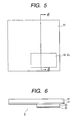
- Fig. 5 is a plan view of EL substrate 6 used in the present invention and Fig. 6 is a sectional view along line 6-6 in Fig. 5 .
- the EL substrate 6 is composed of glass substrate 61, a pair of electrodes disposed on the glass substrate 61, i.e., a transparent electrode 51 and an EL electrode pad 62 of aluminum or the like forming a reflecting surface, and the EL interposed between the pair of electrodes.
- the EL 52 is preferably an organic EL; particularly, either one of those forming REL, GEL, and BEL is placed.
- Materials applicable as the organic ELs in the present invention are those disclosed, for example, in Scozzafava's EPA 349,265 (1990 ); Tang's USP 4,356,429 ; VanSlyke et al.'s USP 4,539,507 ; VanSlyke et al.'s USP 4,720,432 ; Tang et al.'s USP 4,769,292 ; Tang et al.'s USP 4,885,211 ; Perry et al.'s USP 4,950,950 ; Littman et al.'s USP 5,059,861 ; VanSlyke's USP 5,047,687 ; Scozzafava et al.'s USP 5,073,446 ; VanSlyke et al.'s USP 5,059,862 ; VanSlyke et al.'s USP 5,061,617 ; VanSlyke's USP 5,151,629 ; Tang
- the EL layer is comprised of an organic hole injection and transporting zone in contact with the anode, and an electron injection and transporting zone which forms a junction with the organic hole injection and transporting zone.
- the hole injection and transporting zone is made of a single material or plural materials, and comprises a hole injection layer in contact with the anode and a contiguous hole transporting layer interposed between the hole injection layer and the electron injection and transporting zone.
- the electron injection and transporting zone is made of a single material or plural materials, and comprises an electron injecting layer in contact with the cathode and a contiguous electron transporting layer that is interposed between the electron injection layer and the hole injection and transporting zone.
- Recombination of hole and electron and luminescence occurs in the electron injection and transporting zone adjacent to the junction between the electron injection and transporting zone and the hole injection and transporting zone.
- Compounds forming the organic EL layer are deposited typically by vapor deposition, but they may also be deposited by other conventional technologies.
- the organic material of the hole injection layer has the general formula below.
- Q represents N or C-R (where R is hydrogen, alkyl, or halogen), M is a metal, a metal oxide, or a metal halide, and T1, T2 represent hydrogen or both make up an unsaturated six-membered ring containing a substituent such as alkyl or halogen.
- R is hydrogen, alkyl, or halogen
- M is a metal, a metal oxide, or a metal halide
- T1, T2 represent hydrogen or both make up an unsaturated six-membered ring containing a substituent such as alkyl or halogen.
- a preferred alkyl part contains approximately one to six carbon atoms, while phenyl composes a preferred aryl part.
- the hole migration layer is aromatic tertiary amine.
- a preferred subclass of the aromatic tertiary amine contains tetraaryldiamine having the following formula.
- the luminescence, electron injection and transporting zone contains a metal oxinoid compound.
- a preferred example of the metal oxinoid compound has the general formula below.
- R 2 to R 7 represent substitutional possibilities.
- the metal oxinoid compound has the following formula.
- R 2 to R 7 are those defined above, and L1 to L5 collectively contain twelve or fewer carbon atoms, each independently representing hydrogen or a hydrocarbon group of 1 to 12 carbon atoms, wherein L1, L2 together, or L2, L3 together can form a united benzo ring.
- the metal oxinoid compound has the following formula.
- R 2 to R 6 represent hydrogen or other substitutional possibilities.
- the above examples only represent some preferred organic materials simply used in the electroluminescence layer. Those are not described herein for the intention of limiting the scope of the present invention, but generally indicate the organic electroluminescence layer.
- the organic EL materials include the coordinate compounds having the organic ligand.
- the EL anode 62 is deposited on the surface of device.
- the EL anode can be made of any electrically conductive material, but it is preferably made of a material having the work function of 4 eV or less (see the Tang's USP 4,885,211 ). Materials having a low work function are preferable for the anode. It is because they readily release electrons into the electron transporting layer. Metals having the lowest work function are alkali metals, but instability thereof in the air makes use thereof impractical under certain conditions.
- the cathode material is deposited typically by chemical vapor deposition, but other suitable deposition technologies can also be applied.
- the EL cathode is a magnesium : silver alloy of 10 : 1 (in an atomic ratio).
- the cathode layer is applied as a continuous layer over the entire surface of display panel.
- the EL cathode is comprised of a lower layer of a metal with a low work function adjacent to the organic electron injection and transporting zone, and a protective layer overlaid on the metal with the low work function to protect the metal with the low work function from oxygen and humidity.
- the cathode material is opaque, while the anode material is transparent, so that light passes through the anode material.
- light is emitted through the cathode rather than the anode.
- the cathode must be light transmissive and the anode may be opaque.
- a practical balance light transmission and technical conductance is typically in the thickness range of 5 to 25 nm.
- a plastic film can be used instead of the glass substrate 61 used for the EL substrate 6, and ITO or ZnO can be used for the transparent electrode 51.
- the texture structure having fine unevenness in the surface thereof can be employed for the transparent electrode 51.
- the preferred texture structure can be formed by a sputter process under such condition of relatively high temperature that the substrate temperature during deposition of ZnO is 250°C to 300°C.
- the area except for EL 52 in the transparent electrode 51 can be provided with a shield mask (not illustrated).
- the shield mask in this case can be a metal film such as an aluminum film or a chromium film, or a chromium oxide film or an aluminum oxide film for preventing occurrence of reflected light due to these metal films, singly or deposited on the metal film. Since the metal film substantially decreases the resistance of the transparent electrode 51, it is preferred to deposit the metal film on the transparent electrode 51 and further lay the metal oxide film thereon.
- the transparent electrode 51 is set to the earth or a predetermined dc voltage during driving of the EL devices of the present invention.
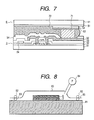
- Fig. 7 is a sectional view of an EL device according to the present invention.
- the EL device is constructed in such structure that TFT substrate 3 and EL substrate 6 are opposed to each other, whereby the EL electrode pad 62 on the EL substrate 6 side and the drain electrode pad 22 on the TFT substrate 3 side are opposed, and that electrical connection is achieved between the both electrodes by adhesive electric connection member 71.
- the adhesive electric connection member 71 is obtained by using an electrically conductive adhesive in which electrically conductive particles such as carbon particles, silver particles, or copper particles are dispersed in an epoxy-based or phenol-based thermosetting adhesive, applying it to a predetermined position of the EL substrate 6 or the TFT substrate 3, or the both by a screen printing method, an offset printing method, or a dispenser applying method, and drying it.
- electrically conductive particles such as carbon particles, silver particles, or copper particles are dispersed in an epoxy-based or phenol-based thermosetting adhesive
- the electrically conductive adhesive described above may contain a silane coupling agent such as N-(2-aminoethyl)-3-aminopropylmethyldimethoxysilane, N-(2-aminoethyl)-3-aminopropyltrimethoxysilane, 3-aminopropyltrimethoxysilane, 3-aminopropylmethyldiethoxysilane, or 3-glycidoxypropyltrimethoxysilane, for enhancing interfacial adhesive strength.
- a silane coupling agent such as N-(2-aminoethyl)-3-aminopropylmethyldimethoxysilane, N-(2-aminoethyl)-3-aminopropyltrimethoxysilane, 3-aminopropyltrimethoxysilane, 3-aminopropylmethyldiethoxysilane, or 3-glycidoxypropyltrimethoxysilane, for enhancing interfa
- Another example of the adhesive electric connection member 71 is solder.
- An adhesive electric insulator 72 is provided around the periphery of the adhesive electric connection member 71 described above.
- the adhesive electric insulator 72 is obtained by applying an epoxy-based or phenol-based insulative adhesive to a predetermined position of the EL substrate 6 or the TFT substrate, or the both by a method such as the offset printing method, the screen printing method, or the dispenser applying method, and drying it.
- a method such as the offset printing method, the screen printing method, or the dispenser applying method, and drying it.
- the above-stated adhesive insulator 72 can be replaced by an insulator having no adhesive strength, for example an organic solvent, and particularly, a high-boiling-point organic solvent or a liquid insulator of liquid crystal such as nematic liquid crystal, cholesteric liquid crystal, or smectic liquid crystal.
- an organic solvent for example an organic solvent, and particularly, a high-boiling-point organic solvent or a liquid insulator of liquid crystal such as nematic liquid crystal, cholesteric liquid crystal, or smectic liquid crystal.
- the aforementioned adhesive insulator 72 or non-adhesive insulator may also contain such a coloring agent as a color pigment or a paint in order to be also provided with the shield effect.
- the EL device of the present invention can be produced by employing a method for applying the conductive adhesive onto the drain electrode pad 22 of TFT substrate 3, for example, by the offset printing method, applying the insulative adhesive to the area (around the periphery of the EL electrode pad 62) except for the EL electrode pad 62 of the EL substrate 6, for example, by the offset printing method, overlaying the EL substrate 6 on the TFT substrate 3 so that the drain electrode pad 22 and the EL electrode pad 62 are opposed to each other, then evacuating the air of the space between the TFT substrate 3 and the EL substrate 6 by an ordinary method, and applying pressure and heat to the both substrates 3 and 6 to fix them in adhesion.
- Fig. 8 shows an evacuating device used on the occasion of evacuation of the air of the space described above.
- TFT substrate 3 and the EL substrate 6 With keeping the TFT substrate 3 and the EL substrate 6 in a superimposed state, they are placed on stage 81, they are covered as illustrated by sheet 83 of plastic film or the like placed between a pair of O-rings 82 and 83 fixed in the periphery, and thereafter vacuum pump 84 is actuated to evacuate the air of the inside of the sheet 83.
- Fig. 9 is an equivalent circuit diagram of another EL device of the present invention.
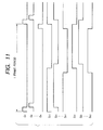
- Fig. 10 and Fig. 11 illustrate an embodiment associated with the sixth, seventh, and eighth features of the present invention.
- G 1 , G 2 , ..., G n are gate on pulses (high-level voltage) successively applied to gate lines connected to the gates of switching devices Tr 1 comprised of thin film transistors, and write rows are selected by successive application of the gate on pulses.
- the gate on pulses G 1 , G 2 , ..., G n being scanning selection signals may be applied either by the interlace scanning method or by the non-interlace scanning method. In the case of the driving by the interlace scanning method, scanning may be the interlace scanning with interlacing of one line or with interlacing of two or more lines.
- S 11 , S 21 ,..., S n1 are control pulses for controlling the emission time of EL, which are applied to the gates of switching devices Tr 3 comprised of thin film transistors during a predetermined emission period.
- the control pulses are applied thereto in, before, or after application of the gate on pulse (high-level voltage) of G 1 , G 2 ,..., G n , and the ELs this time are set in the forward bias state.
- S 12 , S 22 ,..., S n2 interrupt emission of EL and, in order to apply a reverse bias voltage to the ELs through bias control line RB 1 , RB 2 ,..., RB n instead, they are applied as gate on pulses (high-level voltage) to the gates of switching devices Tr 4 comprised of thin film transistors, in, before, or after application of a gate off pulse (low-level voltage) to the switching devices Tr 3 .
- the bias control lines RB 1 , RB 2 ,..., RB n are preferably placed on the EL substrate 6, as shown in Fig. 12 .
- the bias control lines RB 1 , RB 2 ,..., RB n are arranged in such a way that parallel transparent electrodes 511, 512,..., 51n are provided for the respective rows of plural switching devices Tr 1 being active matrix driving devices and each transparent electrode 511, 512,..., 51n is switched independently through gate array 121 to either one of the earth and reverse bias voltage V R .
- the ELs are driven on the occasion of emission of EL so that the potential thereof is set in the forward bias state.
- D 1 , D 2 , D 3 , D 4 ,..., D m (m information lines) supply information signal pulses according to information, applied according to the information to the sources of the switching devices Tr 1 on the columns, and set the forward bias state for the ELs (BELs, GELs, RELs).
- the alternating voltage was applied to each EL and display was achieved by continuous emission over the long term.
- the present invention is suitably applicable to the light-emitting display layer, but the invention can also be applied in place of laser signals, LED signals, or liquid crystal shutter array signals (solid state scanner signals) used in a light signal generator for electrophotographic printer.
- the present invention permitted the EL pixels with high definition, high density, and long life to be produced across a large area and with high productivity.
- the present invention achieved high-luminance light emission of EL and provided the EL devices, based on the high productivity, thus achieving the EL color display with high definition, high density, and continuous high-luminance emission over the long term.
- the present invention provided the EL color display achieving stability against impact and display stability in long-term use.
Landscapes
- Engineering & Computer Science (AREA)
- Microelectronics & Electronic Packaging (AREA)
- Physics & Mathematics (AREA)
- General Physics & Mathematics (AREA)
- Computer Hardware Design (AREA)
- Condensed Matter Physics & Semiconductors (AREA)
- Power Engineering (AREA)
- Theoretical Computer Science (AREA)
- Electroluminescent Light Sources (AREA)
- Devices For Indicating Variable Information By Combining Individual Elements (AREA)
- Thin Film Transistor (AREA)
Abstract
An active matrix electroluminescence device comprises matrix wiring including a plurality of gate scanning lines (G1,G2,...,Gn) and a plurality of information lines (D1,D2,...,Dn) intersecting said plurality of gate scanning lines (G1,G2,...,Gn) as well as a plurality of addressable cells (A'), arranged in rows and in columns, whereby each addressable cell being located a respective matrix address location which is defined by the intersecting of a respective gate scanning line (G1,G2,...,Gn) and a respective information line (D1,D2,...,Dn), and each respective addressable cell including a respective organic electroluminescence element (BEL,GEL,REL) comprised of an organic electroluminescence member. Further, a first thin film transistor (Tr1), the gate of which is connected to the respective gate scanning line (G1,G2,...,Gn) and the first thin film transistor (Tr1) selects the addressable cell according to a pulse applied to the gate scanning line (G1,G2,...,Gn). Moreover, a second thin film transistor (Tr2) for supplying an excitation power to the electroluminescence element (BEL,GEL,REL), and a capacitor (s) for keeping a state in which the second thin film transistor (Tr2) supplies the excitation power to the organic electroluminescence element (BEL,GEL,REL) is characterized in that each row of said matrix wiring includes, in addition to a respective one of said gate scanning lines (G1,G2,...,Gn), a respective gate control line (S11,S21,...,Sn1). Each respective addressable cell further includes a switch (Tr3) for setting a predetermined emission period of the organic electroluminescence element (BEL,GEL,REL) according to a pulse applied to the gate control line (S11,S21,...,Sn1) for every frame interval.
Description
- The present invention relates to an electroluminescence device and an electroluminescence apparatus applicable to display devices, light-emitting sources, or printer heads of electrophotographic printers, and methods for producing them. More particularly, the invention relates to a device and an apparatus using organic electroluminescence members suitable for full-color display of large screen, and methods for producing them.
- The known organic electroluminescence members are, for example, those disclosed in Japanese Laid-Open Patent Applications No.
6-256759 6-136360 6-188074 6-192654 8-41452 - It is also known that these organic electroluminescence members are driven by thin film transistors, for example, as described in Japanese Laid-Open Patent Application No.
8-241048 - For driving the organic electroluminescence members by the thin film transistors, an organic electroluminescence member had to be mounted per drain electrode pad of thin film transistor, however. Particularly, in the case of the full-color display, the electroluminescence members of three kinds for electroluminescence emission of the three primary colors, blue, green, and red, had to be patterned on a thin film transistor substrate. Since the thin film transistor surface had greater unevenness than thin films of the electroluminescence members, it was difficult to pattern the thin films of electroluminescence members in high definition and high density. A further problem was that productivity was low, because the two types of functional devices, the transistors and electroluminescence members, were concentrated on the thin film transistor substrate.
- The organic electroluminescence members had a further problem that long-term application of dc voltage thereto shortened continuous emission time. Particularly, when they were driven by the thin film transistors disclosed in Japanese Laid-Open Patent Application No.
8-241048 - An object of the present invention is to provide a device using organic electroluminescence members suitable for full-color display of large screen, solving the above problems, and a production method thereof.
- Another object of the present invention is to provide an electroluminescence apparatus capable of continuous emission over the long term.
- First, the present invention has the first feature of an electroluminescence device having a transistor substrate comprising thin film transistors arranged along a plurality of rows and columns, gate lines provided for the respective rows, each gate line being a common line for connecting gates of thin film transistors on one of the rows, source lines provided for the respective columns, each source line being a common line for connecting sources of thin film transistors on one of the columns, drain electrode pads each connected to a drain of the respective thin film transistors, and capacitors connected to the respective drain electrode pads; and an electroluminescence substrate comprising pairs of electrodes and electroluminescence members interposed between the pairs of electrodes, which are arranged along a plurality of rows and columns, wherein said thin film transistor substrate and electroluminescence substrate are placed opposite to each other so that the drain electrode pads and the electroluminescence members are opposed to each other, and wherein each drain electrode pad is connected through an adhesive electric connection member to one of a pair of electrodes.
- Second, the present invention has the second feature of an electroluminescence device having a transistor substrate comprising first thin film transistors arranged along a plurality of rows and columns, gate lines provided for the respective rows, each gate line being a common line for connecting gates of first thin film transistors on one of the rows, source lines provided for the respective columns, each source line being a common line for connecting sources of first thin film transistors on one of the columns, second thin film transistors each connected to a drain of the respective first thin film transistors, and capacitors connected to the respective second thin film transistors, wherein a gate of each second thin film transistor is connected to the drain of the first thin film transistor, a drain electrode pad is connected to a drain of each second thin film transistor, and a source of each second thin film transistor is connected to one electrode of the capacitor; and an electroluminescence substrate comprising pairs of electrodes and electroluminescence members interposed between the pairs of electrodes, which are arranged along a plurality of rows and columns, wherein said thin film transistor substrate and electroluminescence substrate are placed opposite to each other so that the drain electrode pads and the electroluminescence members are opposed to each other, and wherein each drain electrode pad is connected through an adhesive electric connection member to one of a pair of electrodes.
- Third, the present invention has the third feature of a production method of electroluminescence device comprising steps of: preparing a transistor substrate comprising thin film transistors arranged along a plurality of rows and columns, gate lines provided for the respective rows, each gate line being a common line for connecting gates of thin film transistors on one of the rows, source lines provided for the respective columns, each source line being a common line for connecting sources of thin film transistors on one of the columns, drain electrode pads each connected to a drain of the respective thin film transistors, and capacitors connected to the respective drain electrode pads; preparing an electroluminescence substrate comprising pairs of electrodes and electroluminescence members interposed between the pairs of electrodes, which are arranged along a plurality of rows and columns; placing an adhesive electric connection member on at least one of the drain electrode pads of the transistor substrate and the electroluminescence members; and overlaying the thin film transistor substrate on the electroluminescence substrate opposite to each other so that the drain electrode pads and the electroluminescence members are opposed to each other.
- Fourth, the present invention has the fourth feature of a production method of electroluminescence device comprising steps of: preparing a transistor substrate comprising thin film transistors arranged along a plurality of rows and columns, gate lines provided for the respective rows, each gate line being a common line for connecting gates of thin film transistors on one of the rows, source lines provided for the respective columns, each source line being a common line for connecting sources of thin film transistors on one of the columns, drain electrode pads each connected to a drain of the respective thin film transistors, and capacitors connected to the respective drain electrode pads; preparing an electroluminescence substrate comprising pairs of electrodes and electroluminescence members interposed between the pairs of electrodes, which are arranged along a plurality of rows and columns; placing an adhesive electric connection member on at least one of the drain electrode pads of the transistor substrate and the electroluminescence members; placing an adhesive electric insulator around the periphery of the adhesive electric connection member on at least one of the drain electrode pads of the transistor substrate and the electroluminescence members; and overlaying the thin film transistor substrate on the electroluminescence substrate opposite to each other so that the drain electrode pads and the electroluminescence members are opposed to each other.
- Fifth, the present invention has the fifth feature of a production method of electroluminescence device comprising steps of: preparing a transistor substrate comprising thin film transistors arranged along a plurality of rows and columns, gate lines provided for the respective rows, each gate line being a common line for connecting gates of thin film transistors on one of the rows, source lines provided for the respective columns, each source line being a common line for connecting sources of thin film transistors on one of the columns, drain electrode pads each connected to a drain of the respective thin film transistors, and capacitors connected to the respective drain electrode pads; preparing an electroluminescence substrate comprising pairs of electrodes and electroluminescence members interposed between the pairs of electrodes, which are arranged along a plurality of rows and columns; placing an adhesive electric connection member on at least one of the drain electrode pads of the transistor substrate and the electroluminescence members; placing an adhesive electric insulator around the periphery of the adhesive electric connection member on at least one of the drain electrode pads of the transistor substrate and the electroluminescence members; overlaying the thin film transistor substrate on the electroluminescence substrate opposite to each other so that the drain electrode pads and the electroluminescence members are opposed to each other; and evacuating a space between the thin film transistor substrate and the electroluminescence substrate and heating the adhesive electric connection member and adhesive electric insulator to cure said member and insulator.
- Sixth, the present invention has the sixth feature of an electroluminescence apparatus having first switching devices arranged along a plurality of rows and columns, first wires provided for the respective rows, each first wire being a common wire for connecting first terminals of first switching devices on a row, second wires provided for the respective columns, each second wire being a common wire connecting second terminals of first switching devices on a column, electroluminescence elements, each having one electrode connected to a third terminal of a first switching device, other electrode, and an electroluminescence member interposed between the one and other electrodes, capacitors connected to the respective third terminals, second switching devices, each being provided between one electrode of an electroluminescence element and a third terminal of a first switching device, third wires connected to the one electrodes of the electroluminescence elements, third switching devices disposed in the third wires, and driving means, said driving means applying a first on signal pulse for turning the first switching devices on, to a first wire of a predetermined row, applying a first off signal pulse for turning the first switching devices off, to the first wires of the other rows, applying an information signal pulse of a forward bias voltage according to information, to the second wires in synchronism with the first on signal pulse, and applying a second on signal pulse for turning the second switching devices on, to a control line for the second switching devices over a predetermined period in, before, or after application of the first on signal pulse for said predetermined row, thereby activating writing into each electroluminescence member on said row; then said driving means applying a second off signal pulse for turning the second switching devices off, to said control line after the predetermined period, applying a third on signal pulse for turning the third switching devices on, to a control line for the third switching devices in, before, or after application of the second off signal pulse, thereby actuating reverse bias applying means set so that a reverse bias voltage is placed between said third wire and the other electrodes of the electroluminescence elements.
- Seventh, the present invention has the seventh feature of an electroluminescence apparatus having first thin film transistors arranged along a plurality of rows and columns, first wires provided for the respective rows, each first wire being a common wire for connecting gates of first thin film transistors on a row, second wires provided for the respective columns, each second wire being a common wire for connecting sources of first thin film transistors on a column, electroluminescence elements, each having one electrode connected to a drain of a first thin film transistor, other electrode, and an electroluminescence member interposed between the one and other electrodes, second thin film transistors connected at gates thereof, each being provided between said drain and one electrode of the electroluminescence element, capacitors connected to the respective drains, first switching devices, each being provided between one electrode of an electroluminescence element and a drain electrode of a second thin film transistor, third wires, each being connected to one electrode of an electroluminescence element, second switching devices provided in said third wires, and driving means, said driving means applying a first on signal pulse for turning the first thin film transistors on, to a first wire of a predetermined row, applying a first off signal pulse for turning the first thin film transistors off, to the first wires of the other rows, applying an information signal pulse of a forward bias voltage according to information, to the second wires in synchronism with the first on signal pulse, and applying a second on signal pulse for turning the first switching devices on, to a control line for the first switching devices over a predetermined period in, before, or after application of the first on signal pulse for said predetermined row, thereby activating writing into each electroluminescence member on said row; then said driving means applying a second off signal pulse for turning the first switching devices off, to said control line after the predetermined period, and applying a third on signal pulse for turning the second switching devices on, to a control line for the third switching devices in, before, or after application of the second off signal pulse, thereby actuating reverse bias applying means set so that a reverse bias voltage is placed between said third wire and the other electrodes of the electroluminescence elements.
- Eighth, the present invention has the eighth feature of an electroluminescence apparatus having: switching devices arranged along a plurality of columns and rows, first wires provided for the respective rows, each first wire being a common wire for connecting first terminals of switching devices on a row, second wires provided for the respective columns, each second wire being a common wire for connecting second terminals of switching devices on a column, and electroluminescence elements, each having one electrode connected to a third terminal of a switching device, other electrode, and an electroluminescence member interposed between the one and other electrodes; and driving means, said driving means applying a scanning selection pulse for selecting at least one row out of said plurality of rows, to a first wire corresponding to the selected row, applying an information signal pulse for bringing the electroluminescence members into a forward bias state according to information, to each of the second wires in synchronism with the scanning selection signal, and applying a bias voltage for bringing the electroluminescence members into a reverse bias state, through a third wire to the electroluminescence members before start of application of a next scanning selection signal or a scanning selection signal thereafter to the first wire corresponding to said selected row.
-
-
Fig. 1 is an equivalent circuit diagram of an EL device of the present invention; -
Fig. 2 is a plan view of an EL pixel on the TFT substrate side, used in the EL device of the present invention; -
Fig. 3 is a sectional view along line 3-3 inFig. 2 ; -
Fig. 4 is a sectional view along line 4-4 inFig. 2 : -
Fig. 5 is a plan view of an EL pixel on the EL substrate side, used in the EL device of the present invention; -
Fig. 6 is a sectional view along line 6-6 inFig. 5 ; -
Fig. 7 is a sectional view of an EL device of the present invention; -
Fig. 8 is a sectional view of an evacuation system used in the method of the present invention; -
Fig. 9 is an equivalent circuit diagram of another EL device of the present invention; -
Fig. 10 is an equivalent circuit diagram of an EL apparatus used in another embodiment of the present invention; -
Fig. 11 is a timing chart of driving used in the present invention; and -
Fig. 12 is a plan view of an EL substrate used in the present invention. - The electroluminescence members are preferably media that emit the three primary colors of blue, green, and red; particularly, organic electroluminescence members.
- The adhesive electric connection member is preferably a material in which electrically conductive particles are dispersed in an adhesive, and particularly preferably, a material containing a silane coupling agent.
- It is preferable to employ a bond structure in which an adhesive electric insulator is disposed around the periphery of the adhesive electric connection member.
- The thin film transistors are preferably of a polysilicon semiconductor, a crystal silicon semiconductor, a microcrystal silicon semiconductor, or an amorphous silicon semiconductor.
- At least one electrode out of a pair of electrodes on either side of the electroluminescence member is preferably a transparent electrode of ZnO having the texture structure.
- The sixth, seventh, and eighth features of the present invention permit the alternating voltage to be applied to the electroluminescence elements in active matrix driving, thereby greatly extending the continuous emission time of the organic electroluminescence members over the long term in particular.
- The predetermined period used in the present invention is a period equal to 1/4 to 3/4 of one vertical scanning period (one frame period or one field period), preferably a period equal to 1/3 to 2/3 thereof, and particularly optimally, a period equal to approximately 1/2 thereof.
- A time average voltage of the forward bias voltage and reverse bias voltage used in the present invention is preferably set to approximately zero.
- The present invention will be described by reference to the drawings. In the following description, the thin film transistor described above will be denoted by "TFT" and the electroluminescence member by "EL."
-
Fig. 1 is a schematic diagram of an active matrix four-terminal TFT-EL device. A device of each pixel includes two TFTs, a storage capacitor, and an EL device. A principal feature of the four-terminal type is the capability of separating an addressing signal from an EL excitation signal. The EL device is selected through the logic TFT (T1) and excitation power to the EL device is controlled by the power TFT (T2). The storage capacitor makes it possible to keep the excitation power staying in the addressed EL device once selected. Thus the circuit permits the EL device to operate at the duty cycle close to 100 %, ignoring the time assigned to addressing. - Gate lines Yj, Yj+1 are preferably a lot of wires, for example 640 wires or 1120 wires, to which gate pulses are applied in order. The gate pulses may be of either interlace scanning or non-interlace scanning.
- Source lines Xi, Xi+1, Xi+2 are preferably a lot of wires, for example 840 wires or 1280 wires, to which information signal pulses of a voltage set according to image data are applied in synchronism with the gate pulses.
- In the drawing REL designates red-emitting EL, GEL green-emitting EL, and BEL blue-emitting EL; information signal pulses of red are applied to the source line Xi, green information pulses to Xi+1, and blue information pulses to Xi+2. This achieves the full-color display.
-
Fig. 2 is a plan view to show a typical example ofTFT substrate 3 according to the present invention.TFT 1 corresponds to T1 ofFig. 1 ,TFT 2 to T2 ofFig. 1 ,capacitor 21 to Cs ofFig. 1 , anddrain electrode pad 22 to an electrode connected to the drain of T2 in each EL ofFig. 1 . -
Fig. 3 is a sectional view along line 3-3 inFig. 2 .Fig. 4 is a sectional view along line 4-4 inFig. 2 . - TFT 1 and TFT 2 used in the present invention have such transistor structure that
source bus 24 is connected to n+ polysilicon, the drain to n+ polysilicon, PECVD (plasma-enhanced CVD)-SiO2film 32 is placed as a gate insulating film on either side of the i-type polysilicon film, and the gate bus is connected to n+ polysilicon. - The present invention is not limited to the aforementioned transistor structure, but may adopt either the stagger structure or the coplanar structure using amorphous silicon or microcrystalline silicon semiconductors.
- The present invention can be applied to MOS transistors of the SOI (silicon on insulator) structure using crystal silicon.
- The capacitor Cs is composed of a pair of
capacitor electrodes Fig. 4 . Thecapacitor electrode 41 is a film formed of Al or the like and connected to theground bus 25, while thecapacitor electrode 42 is a film formed of n+ polysilicon and connected to the drain ofTFT 2. - The
gate bus 23 andsource bus 24 are preferably chromium/aluminum layered wires. - A
passivation film 34 is preferably a film of silicon nitride formed by plasma CVD. - A metal film of aluminum, silver, or the like can be used as the
drain electrode pad 22 in order to provide it with reflecting performance, but a transparent conductive film such as ITO or ZnO may also be applied. -
Fig. 5 is a plan view ofEL substrate 6 used in the present invention andFig. 6 is a sectional view along line 6-6 inFig. 5 . - The
EL substrate 6 is composed ofglass substrate 61, a pair of electrodes disposed on theglass substrate 61, i.e., atransparent electrode 51 and anEL electrode pad 62 of aluminum or the like forming a reflecting surface, and the EL interposed between the pair of electrodes. - The
EL 52 is preferably an organic EL; particularly, either one of those forming REL, GEL, and BEL is placed. - Specific examples of REL, GEL, and BEL are listed below, but it is noted that the present invention is not intended to be limited to these examples and that inorganic ELs can also be applied instead of the organic ELs.
- Materials applicable as the organic ELs in the present invention are those disclosed, for example, in
Scozzafava's EPA 349,265 (1990 Tang's USP 4,356,429 ;VanSlyke et al.'s USP 4,539,507 ;VanSlyke et al.'s USP 4,720,432 ;Tang et al.'s USP 4,769,292 ;Tang et al.'s USP 4,885,211 ;Perry et al.'s USP 4,950,950 ;Littman et al.'s USP 5,059,861 ;VanSlyke's USP 5,047,687 ;Scozzafava et al.'s USP 5,073,446 ;VanSlyke et al.'s USP 5,059,862 ;VanSlyke et al.'s USP 5,061,617 ;VanSlyke's USP 5,151,629 ;Tang et al.'s USP 5,294,869 ;Tang et al.'s USP 5,294,870 . The EL layer is comprised of an organic hole injection and transporting zone in contact with the anode, and an electron injection and transporting zone which forms a junction with the organic hole injection and transporting zone. The hole injection and transporting zone is made of a single material or plural materials, and comprises a hole injection layer in contact with the anode and a contiguous hole transporting layer interposed between the hole injection layer and the electron injection and transporting zone. Similarly, the electron injection and transporting zone is made of a single material or plural materials, and comprises an electron injecting layer in contact with the cathode and a contiguous electron transporting layer that is interposed between the electron injection layer and the hole injection and transporting zone. Recombination of hole and electron and luminescence occurs in the electron injection and transporting zone adjacent to the junction between the electron injection and transporting zone and the hole injection and transporting zone. Compounds forming the organic EL layer are deposited typically by vapor deposition, but they may also be deposited by other conventional technologies. - In a preferred embodiment the organic material of the hole injection layer has the general formula below.

- In the above formula, Q represents N or C-R (where R is hydrogen, alkyl, or halogen), M is a metal, a metal oxide, or a metal halide, and T1, T2 represent hydrogen or both make up an unsaturated six-membered ring containing a substituent such as alkyl or halogen. A preferred alkyl part contains approximately one to six carbon atoms, while phenyl composes a preferred aryl part.
- In a preferred embodiment the hole migration layer is aromatic tertiary amine. A preferred subclass of the aromatic tertiary amine contains tetraaryldiamine having the following formula.

- In the above formula Are represents arylene, n an integer from 1 to 4, and Ar, R7, R8, R9 each an aryl group selected. In a preferred embodiment the luminescence, electron injection and transporting zone contains a metal oxinoid compound. A preferred example of the metal oxinoid compound has the general formula below.

- In this formula R2 to R7 represent substitutional possibilities. In another preferred embodiment the metal oxinoid compound has the following formula.

- In the above formula R2 to R7 are those defined above, and L1 to L5 collectively contain twelve or fewer carbon atoms, each independently representing hydrogen or a hydrocarbon group of 1 to 12 carbon atoms, wherein L1, L2 together, or L2, L3 together can form a united benzo ring. In another preferred embodiment the metal oxinoid compound has the following formula.

- In this formula R2 to R6 represent hydrogen or other substitutional possibilities. The above examples only represent some preferred organic materials simply used in the electroluminescence layer. Those are not described herein for the intention of limiting the scope of the present invention, but generally indicate the organic electroluminescence layer. As understood from the above examples, the organic EL materials include the coordinate compounds having the organic ligand.
- In the next process stage the
EL anode 62 is deposited on the surface of device. The EL anode can be made of any electrically conductive material, but it is preferably made of a material having the work function of 4 eV or less (see theTang's USP 4,885,211 ). Materials having a low work function are preferable for the anode. It is because they readily release electrons into the electron transporting layer. Metals having the lowest work function are alkali metals, but instability thereof in the air makes use thereof impractical under certain conditions. The cathode material is deposited typically by chemical vapor deposition, but other suitable deposition technologies can also be applied. It was found that a particularly preferred material for the EL cathode is a magnesium : silver alloy of 10 : 1 (in an atomic ratio). Preferably, the cathode layer is applied as a continuous layer over the entire surface of display panel. In another embodiment the EL cathode is comprised of a lower layer of a metal with a low work function adjacent to the organic electron injection and transporting zone, and a protective layer overlaid on the metal with the low work function to protect the metal with the low work function from oxygen and humidity. - Typically the cathode material is opaque, while the anode material is transparent, so that light passes through the anode material. However, in an alternative embodiment light is emitted through the cathode rather than the anode. In this case the cathode must be light transmissive and the anode may be opaque. A practical balance light transmission and technical conductance is typically in the thickness range of 5 to 25 nm.
- In the present invention a plastic film can be used instead of the
glass substrate 61 used for theEL substrate 6, and ITO or ZnO can be used for thetransparent electrode 51. - In order to increase the surface area of
EL 52, the texture structure having fine unevenness in the surface thereof can be employed for thetransparent electrode 51. The preferred texture structure can be formed by a sputter process under such condition of relatively high temperature that the substrate temperature during deposition of ZnO is 250°C to 300°C. - The area except for
EL 52 in thetransparent electrode 51 can be provided with a shield mask (not illustrated). The shield mask in this case can be a metal film such as an aluminum film or a chromium film, or a chromium oxide film or an aluminum oxide film for preventing occurrence of reflected light due to these metal films, singly or deposited on the metal film. Since the metal film substantially decreases the resistance of thetransparent electrode 51, it is preferred to deposit the metal film on thetransparent electrode 51 and further lay the metal oxide film thereon. - The
transparent electrode 51 is set to the earth or a predetermined dc voltage during driving of the EL devices of the present invention. -
Fig. 7 is a sectional view of an EL device according to the present invention. The EL device is constructed in such structure thatTFT substrate 3 andEL substrate 6 are opposed to each other, whereby theEL electrode pad 62 on theEL substrate 6 side and thedrain electrode pad 22 on theTFT substrate 3 side are opposed, and that electrical connection is achieved between the both electrodes by adhesiveelectric connection member 71. - The adhesive
electric connection member 71 is obtained by using an electrically conductive adhesive in which electrically conductive particles such as carbon particles, silver particles, or copper particles are dispersed in an epoxy-based or phenol-based thermosetting adhesive, applying it to a predetermined position of theEL substrate 6 or theTFT substrate 3, or the both by a screen printing method, an offset printing method, or a dispenser applying method, and drying it. - The electrically conductive adhesive described above may contain a silane coupling agent such as N-(2-aminoethyl)-3-aminopropylmethyldimethoxysilane, N-(2-aminoethyl)-3-aminopropyltrimethoxysilane, 3-aminopropyltrimethoxysilane, 3-aminopropylmethyldiethoxysilane, or 3-glycidoxypropyltrimethoxysilane, for enhancing interfacial adhesive strength.
- Another example of the adhesive
electric connection member 71 is solder. - An adhesive
electric insulator 72 is provided around the periphery of the adhesiveelectric connection member 71 described above. The adhesiveelectric insulator 72 is obtained by applying an epoxy-based or phenol-based insulative adhesive to a predetermined position of theEL substrate 6 or the TFT substrate, or the both by a method such as the offset printing method, the screen printing method, or the dispenser applying method, and drying it. On this occasion, in applying the insulative adhesive and the conductive adhesive, it is preferred to employ a production method for laying the insulative adhesive on either one of theEL substrate 6 and theTFT substrate 3 and laying the conductive adhesive on the other substrate without the insulative adhesive. - In the present invention, the above-stated
adhesive insulator 72 can be replaced by an insulator having no adhesive strength, for example an organic solvent, and particularly, a high-boiling-point organic solvent or a liquid insulator of liquid crystal such as nematic liquid crystal, cholesteric liquid crystal, or smectic liquid crystal. - The aforementioned
adhesive insulator 72 or non-adhesive insulator may also contain such a coloring agent as a color pigment or a paint in order to be also provided with the shield effect. - The EL device of the present invention can be produced by employing a method for applying the conductive adhesive onto the
drain electrode pad 22 ofTFT substrate 3, for example, by the offset printing method, applying the insulative adhesive to the area (around the periphery of the EL electrode pad 62) except for theEL electrode pad 62 of theEL substrate 6, for example, by the offset printing method, overlaying theEL substrate 6 on theTFT substrate 3 so that thedrain electrode pad 22 and theEL electrode pad 62 are opposed to each other, then evacuating the air of the space between theTFT substrate 3 and theEL substrate 6 by an ordinary method, and applying pressure and heat to the bothsubstrates -
Fig. 8 shows an evacuating device used on the occasion of evacuation of the air of the space described above. With keeping theTFT substrate 3 and theEL substrate 6 in a superimposed state, they are placed onstage 81, they are covered as illustrated bysheet 83 of plastic film or the like placed between a pair of O-rings vacuum pump 84 is actuated to evacuate the air of the inside of thesheet 83. -
Fig. 9 is an equivalent circuit diagram of another EL device of the present invention. -
Fig. 10 andFig. 11 illustrate an embodiment associated with the sixth, seventh, and eighth features of the present invention. - G1, G2, ..., Gn (n gate scanning lines) are gate on pulses (high-level voltage) successively applied to gate lines connected to the gates of switching devices Tr1 comprised of thin film transistors, and write rows are selected by successive application of the gate on pulses. The gate on pulses G1, G2, ..., Gn being scanning selection signals may be applied either by the interlace scanning method or by the non-interlace scanning method. In the case of the driving by the interlace scanning method, scanning may be the interlace scanning with interlacing of one line or with interlacing of two or more lines.
- S11, S21,..., Sn1 are control pulses for controlling the emission time of EL, which are applied to the gates of switching devices Tr3 comprised of thin film transistors during a predetermined emission period. The control pulses are applied thereto in, before, or after application of the gate on pulse (high-level voltage) of G1, G2,..., Gn, and the ELs this time are set in the forward bias state.
- S12, S22,..., Sn2 interrupt emission of EL and, in order to apply a reverse bias voltage to the ELs through bias control line RB1, RB2,..., RBn instead, they are applied as gate on pulses (high-level voltage) to the gates of switching devices Tr4 comprised of thin film transistors, in, before, or after application of a gate off pulse (low-level voltage) to the switching devices Tr3.
- The bias control lines RB1, RB2,..., RBn are preferably placed on the
EL substrate 6, as shown inFig. 12 . In this case, the bias control lines RB1, RB2,..., RBn are arranged in such a way that paralleltransparent electrodes transparent electrode gate array 121 to either one of the earth and reverse bias voltage VR. Based on this arrangement, the ELs are driven on the occasion of emission of EL so that the potential thereof is set in the forward bias state. - In
Fig. 10 D1, D2, D3, D4,..., Dm (m information lines) supply information signal pulses according to information, applied according to the information to the sources of the switching devices Tr1 on the columns, and set the forward bias state for the ELs (BELs, GELs, RELs). - According to the sixth, seventh, and eighth features of the present invention, the alternating voltage was applied to each EL and display was achieved by continuous emission over the long term.
- The present invention is suitably applicable to the light-emitting display layer, but the invention can also be applied in place of laser signals, LED signals, or liquid crystal shutter array signals (solid state scanner signals) used in a light signal generator for electrophotographic printer.
- The present invention permitted the EL pixels with high definition, high density, and long life to be produced across a large area and with high productivity.
- The present invention achieved high-luminance light emission of EL and provided the EL devices, based on the high productivity, thus achieving the EL color display with high definition, high density, and continuous high-luminance emission over the long term.
- Further, the present invention provided the EL color display achieving stability against impact and display stability in long-term use.
- This application is a divisional application of European patent application no.
98 304 275.5 EP 0 883 191 . The original claims of the parent application are repeated below in the present specification and form part of the content of this divisional application as filed. - 1. An electroluminescence device having a transistor substrate comprising thin film transistors arranged along a plurality of rows and columns, gate lines provided for the respective rows, each gate line being a common line for connecting gates of thin film transistors on one of the rows, source lines provided for the respective columns, each source line being a common line for connecting sources of thin film transistors on one of the columns, drain electrode pads each connected to a drain of the respective thin film transistors, and capacitors connected to the respective drain electrode pads; and an electroluminescence substrate comprising pairs of electrodes and electroluminescence members interposed between the pairs of electrodes, which are arranged along a plurality of rows and columns, wherein said thin film transistor substrate and electroluminescence substrate are placed opposite to each other so that the drain electrode pads and the electroluminescence members are opposed to each other, and wherein each drain electrode pad is connected through an adhesive electric connection member to one of a pair of electrodes of said electroluminescence member.
- 2. An electroluminescence device having a transistor substrate comprising first thin film transistors arranged along a plurality of rows and columns, gate lines provided for the respective rows, each gate line being a common line for connecting gates of first thin film transistors on one of the rows, source lines provided for the respective columns, each source line being a common line for connecting sources of first thin film transistors on one of the columns, second thin film transistors each connected to a drain of the respective first thin film transistors, and capacitors connected to the respective second thin film transistors, wherein a gate of each second thin film transistor is connected to the drain of the first thin film transistor, a drain electrode pad is connected to a drain of each second thin film transistor, and a source of each second thin film transistor is connected to one electrode of the capacitor; and an electroluminescence substrate comprising pairs of electrodes and electroluminescence members interposed between the pairs of electrodes, which are arranged along a plurality of rows and columns, wherein said thin film transistor substrate and electroluminescence substrate are placed opposite to each other so that the drain electrode pads and the electroluminescence members are opposed to each other, and wherein each drain electrode pad is connected through an adhesive electric connection member to one of a pair of electrodes of said electroluminescence member.
- 3. The electroluminescence device according to either of
claims - 4. The electroluminescence device according to either of
claims - 5. The electroluminescence device according to either of
claims - 6. The electroluminescence device according to either of
claims - 7. The electroluminescence device according to either of
claims - 8. The electroluminescence device according to either of
claims - 9. The electroluminescence device according to
claim 1, wherein an electric insulator containing a coloring agent is disposed around the periphery of said adhesive electric connection member. - 10. The electroluminescence device according to
claim 1, wherein an electric insulator of a liquid form is disposed around the periphery of said adhesive electric connection member. - 11. The electroluminescence device according to either of
claims - 12. The electroluminescence device according to either of
claims - 13. The electroluminescence device according to either of
claims - 14. The electroluminescence device according to
claim 1, wherein at least one electrode out of the pair of electrodes on either side of each said electroluminescence member is a transparent electrode having a texture structure. - 15. The electroluminescence device according to
claim 1, wherein at least one electrode out of the pair of electrodes on either side of each said electroluminescence member is a transparent electrode of Zn0 having the texture structure. - 16. A production method of electroluminescence device comprising steps of:
- preparing a transistor substrate comprising thin film transistors arranged along a plurality of rows and columns, gate lines provided for the respective rows, each gate line being a common line for connecting gates of thin film transistors on one of the rows, source lines provided for the respective columns, each source line being a common line for connecting sources of thin film transistors on one of the columns, drain electrode pads each connected to a drain of the respective thin film transistors, and capacitors connected to the respective drain electrode pads;
- preparing an electroluminescence substrate comprising pairs of electrodes and electroluminescence members interposed between the pairs of electrodes, which are arranged along a plurality of rows and columns;
- placing an adhesive electric connection member on at least one of the drain electrode pads of the transistor substrate and the electroluminescence members; and
- overlaying the thin film transistor substrate on the electroluminescence substrate opposite to each other so that the drain electrode pads and the electroluminescence members are opposed to each other.
- 17. The production method of electroluminescence device according to claim 16, wherein said electroluminescence members comprise media that emit the three primary colors of blue, green and red.
- 18. The production method of electroluminescence device according to Claim 16, wherein said electroluminescence members comprise media of organic substance that emit the three primary colors of blue, green and red.
- 19. The production method of electroluminescence device according to Claim 16, wherein said adhesive electric connection member is a material in which electrically conductive particles are dispersed in an adhesive.
- 20. The production method of electroluminescence device according to Claim 19, wherein said adhesive electric connection member is a material in which the electrically conductive particles are dispersed in the adhesive and which contains a silane coupling agent.
- 21. A production method of electroluminescence device comprising steps of:
- preparing a transistor substrate comprising thin film transistors arranged along a plurality of rows and columns, gate lines provided for the respective rows, each gate line being a common line for connecting gates of thin film transistors on one of the rows, source lines provided for the respective columns, each source line being a common line for connecting sources of thin film transistors on one of the columns, drain electrode pads each connected to a drain of the respective thin film transistors, and capacitors connected to the respective drain electrode pads;
- preparing an electroluminescence substrate comprising pairs of electrodes and electroluminescence members interposed between the pairs of electrodes, which are arranged along a plurality of rows and columns;
- placing an adhesive electric connection member on at least one of the drain electrode pads of the transistor substrate and the electroluminescence members;
- placing an adhesive electric insulator around the periphery of the adhesive electric connection member on at least one of the drain electrode pads of the transistor substrate and the electroluminescence members; and
- overlaying the thin film transistor substrate on the electroluminescence substrate opposite to each other so that the drain electrode pads and the electroluminescence members are opposed to each other.
- 22. A production method of electroluminescence device comprising steps of:
- preparing a transistor substrate comprising thin film transistors arranged along a plurality of rows and columns, gate lines provided for the respective rows, each gate line being a common line for connecting gates of thin film transistors on one of the rows, source lines provided for the respective columns, each source line being a common line for connecting sources of thin film transistors on one of the columns, drain electrode pads each connected to a drain of the respective thin film transistors, and capacitors connected to the respective drain electrode pads;
- preparing an electroluminescence substrate comprising pairs of electrodes and electroluminescence members interposed between the pairs of electrodes, which are arranged along a plurality of rows and columns;
- placing an adhesive electric connection member on at least one of the drain electrode pads of the transistor substrate and the electroluminescence members;
- placing an adhesive electric insulator around the periphery of the adhesive electric connection member on at least one of the drain electrode pads of the transistor substrate and the electroluminescence members;
- overlaying the thin film transistor substrate on the electroluminescence substrate opposite to each other so that the drain electrode pads and the electroluminescence members are opposed to each other; and
- evacuating a space between the thin film transistor substrate and the electroluminescence substrate and heating the adhesive electric connection member and adhesive electric insulator to cure said member and insulator.
- 23. An electroluminescence apparatus having first switching devices arranged along a plurality of rows and columns, first wires provided for the respective rows, each first wire being a common wire for connecting first terminals of first switching devices on a row, second wires provided for the respective columns, each second wire being a common wire connecting second terminals of first switching devices on a column, electroluminescence elements, each having one electrode connected to a third terminal of a first switching device, other electrode, and an electroluminescence member interposed between the one and other electrodes, capacitors connected to the respective third terminals, second switching devices, each being provided between one electrode of an electroluminescence element and a third terminal of a first switching device, third wires connected to the one electrodes of the electroluminescence elements, third switching devices disposed in the third wires, and driving means, said driving means applying a first on signal pulse for turning the first switching devices on, to a first wire of a predetermined row, applying a first off signal pulse for turning the first switching devices off, to the first wires of the other rows, applying an information signal pulse of a forward bias voltage according to information, to the second wires in synchronism with the first on signal pulse, and applying a second on signal pulse for turning the second switching devices on, to a control line for the second switching devices over a predetermined period in, before, or after application of the first on signal pulse for said predetermined row, thereby activating writing into each electroluminescence member on said row; then said driving means applying a second off signal pulse for turning the second switching devices off, to said control line after the predetermined period, applying a third on signal pulse for turning the third switching devices on, to a control line for the third switching devices in, before, or after application of the second off signal pulse, thereby actuating reverse bias applying means set so that a reverse bias voltage is placed between said third wire and the other electrodes of the electroluminescence elements.
- 24. An electroluminescence apparatus having first thin film transistors arranged along a plurality of rows and columns, first wires provided for the respective rows, each first wire being a common wire for connecting gates of first thin film transistors on a row, second wires provided for the respective columns, each second wire being a common wire for connecting sources of first thin film transistors on a column, electroluminescence elements, each having one electrode connected to a drain of a first thin film transistor, other electrode, and an electroluminescence member interposed between the one and other electrodes, second thin film transistors connected at gates thereof, each being provided between said drain and one electrode of the electroluminescence element, capacitors connected to the respective drains, first switching devices, each being provided between one electrode of an electroluminescence element and a drain electrode of a second thin film transistor, third wires, each being connected to one electrode of an electroluminescence element, second switching devices provided in said third wires, and driving means, said driving means applying a first on signal pulse for turning the first thin film transistors on, to a first wire of a predetermined row, applying a first off signal pulse for turning the first thin film transistors off, to the first wires of the other rows, applying an information signal pulse of a forward bias voltage according to information, to the second wires in synchronism with the first on signal pulse, and applying a second on signal pulse for turning the first switching devices on, to a control line for the first switching devices over a predetermined period in, before, or after application of the first on signal pulse for said predetermined row, thereby activating writing into each electroluminescence member on said row; then said driving means applying a second off signal pulse for turning the first switching devices off, to said control line after the predetermined period, and applying a third on signal pulse for turning the second switching devices on, to a control line for the third switching devices in, before, or after application of the second off signal pulse, thereby actuating reverse bias applying means set so that a reverse bias voltage is placed between said third wire and the other electrodes of the electroluminescence elements.
- 25. The electroluminescence apparatus according to either of
claims - 26. The electroluminescence apparatus according to either of
claims - 27. The electroluminescence apparatus according to
claim 23, wherein said first, second, and third switching devices are thin film transistors. - 28. The electroluminescence apparatus according to
claim 23, wherein said first, second, and third switching devices are thin film transistors, said first terminals are gate terminals, said second terminals are source terminals, and said third terminals are drain terminals. - 29. The electroluminescence apparatus according to either of
claims - 30. The electroluminescence apparatus according to either of
claims - 31. The electroluminescence apparatus according to either of
claims - 32. The electroluminescence apparatus according to either of
claims - 33. The electroluminescence apparatus according to either of
claims - 34. The electroluminescence apparatus according to either of
claims - 35. The electroluminescence apparatus according to
claim 24, wherein said first and second switching devices are thin film transistors. - 36. The electroluminescence apparatus according to
claim 24, wherein the sources of said second thin film transistors and the one electrodes of said capacitors are set to an equal voltage. - 37. The electroluminescence apparatus according to
claim 24, wherein the sources of said second thin film transistors and the one electrodes of said capacitors are connected by fourth wires, said apparatus comprising means for applying a voltage to said fourth wires. - 38. An electroluminescence apparatus having:
- switching devices arranged along a plurality of columns and rows, first wires provided for the respective rows, each first wire being a common wire for connecting first terminals of switching devices on a row, second wires provided for the respective columns, each second wire being a common wire for connecting second terminals of switching devices on a column, and electroluminescence elements, each having one electrode connected to a third terminal of a switching device, other electrode, and an electroluminescence member interposed between the one and other electrodes; and
- driving means, said driving means applying a scanning selection pulse for selecting at least one row out of said plurality of rows, to a first wire corresponding to the selected row, applying an information signal pulse for bringing the electroluminescence members into a forward bias state according to information, to each of the second wires in synchronism with the scanning selection signal, and applying a bias voltage for bringing the electroluminescence members into a reverse bias state, through a third wire to the electroluminescence members before start of application of a next scanning selection signal or a scanning selection signal thereafter to the first wire corresponding to said selected row.
- 39. The electroluminescence apparatus according to any of
claims - 40. The electroluminescence apparatus according to claim 38, wherein a capacitor is connected to said third terminal.
Claims (1)
- An active matrix electroluminescence device comprising:matrix wiring including a plurality of gate scanning lines (G1, G2,..Gn) and a plurality of information lines (D1, O2,..On) intersecting said plurality of gate scanning lines (G1, G2,..Gn); anda plurality of addressable cells (A'), arranged in rows and in columns, each addressable cell being located a respective matrix address location which is defined by the intersecting of a respective gate scanning line (G1, G2,..Gn) and a respective information line (D1, D2,..Dn), each respective addressable cell including a respective organic electroluminescence element (BEL, GEL, REL) comprised of an organic electroluminescence member,a first thin film transistor (Tr1), the gate of which is connected to the respective gate scanning line (G1, G2,..Gn) and the first thin film transistor (Tr1) selects the addressable cell according to a pulse applied to the gate scanning line,a second thin film transistor (Tr2) for supplying an excitation power to the electroluminescence element, and a capacitor (Cs) for keeping a state in which the second thin film transistor supplies the excitation power to the organic electroluminescence element,characterized in that:each row of said matrix wiring includes, in addition to a respective one of said gate scanning lines (G1, G2,..Gn), a respective gate control line (S11, S21,.., Sn1); andeach respective addressable cell further includes a switch for setting a predetermined emission period of the organic electroluminescence element according to a pulse applied to the gate control line for every frame interval.
Applications Claiming Priority (3)
| Application Number | Priority Date | Filing Date | Title |
|---|---|---|---|
| JP9143836A JPH10333601A (en) | 1997-06-02 | 1997-06-02 | Electroluminescent element and its manufacture |
| JP9152309A JPH113048A (en) | 1997-06-10 | 1997-06-10 | Electroluminescent element and device and their production |
| EP98304275A EP0883191A3 (en) | 1997-06-02 | 1998-05-29 | Electroluminescence device, electroluminescence apparatus, and production methods thereof |
Related Parent Applications (1)
| Application Number | Title | Priority Date | Filing Date |
|---|---|---|---|
| EP98304275A Division EP0883191A3 (en) | 1997-06-02 | 1998-05-29 | Electroluminescence device, electroluminescence apparatus, and production methods thereof |
Publications (1)
| Publication Number | Publication Date |
|---|---|
| EP2151865A1 true EP2151865A1 (en) | 2010-02-10 |
Family
ID=26475459
Family Applications (2)
| Application Number | Title | Priority Date | Filing Date |
|---|---|---|---|
| EP09172441A Withdrawn EP2151865A1 (en) | 1997-06-02 | 1998-05-29 | Electroluminescence device, electroluminescence apparatus, and production methods thereof |
| EP98304275A Withdrawn EP0883191A3 (en) | 1997-06-02 | 1998-05-29 | Electroluminescence device, electroluminescence apparatus, and production methods thereof |
Family Applications After (1)
| Application Number | Title | Priority Date | Filing Date |
|---|---|---|---|
| EP98304275A Withdrawn EP0883191A3 (en) | 1997-06-02 | 1998-05-29 | Electroluminescence device, electroluminescence apparatus, and production methods thereof |
Country Status (2)
| Country | Link |
|---|---|
| US (2) | US6175345B1 (en) |
| EP (2) | EP2151865A1 (en) |
Cited By (9)
| Publication number | Priority date | Publication date | Assignee | Title |
|---|---|---|---|---|
| US7710028B2 (en) | 1999-09-03 | 2010-05-04 | Semiconductor Energy Laboratory Co., Ltd. | EL display device having pixel electrode with projecting portions and manufacturing method thereof |
| US7880380B2 (en) | 2003-06-17 | 2011-02-01 | Semiconductor Energy Laboratory Co., Ltd. | Display device and electronic apparatus |
| US8017948B2 (en) | 1999-11-30 | 2011-09-13 | Semiconductor Energy Laboratory Co., Ltd. | Electric device |
| US8129900B2 (en) | 2003-09-19 | 2012-03-06 | Semiconductor Energy Laboratory Co., Ltd. | Display device and method for manufacturing the same |
| US8395604B2 (en) | 2005-01-21 | 2013-03-12 | Semiconductor Energy Laboratory Co., Ltd. | Semiconductor device, display device and electronic apparatus |
| US8736520B2 (en) | 1999-10-21 | 2014-05-27 | Semiconductor Energy Laboratory Co., Ltd. | Electro-optical device |
| US8896506B2 (en) | 2001-10-30 | 2014-11-25 | Semiconductor Energy Laboratory Co., Ltd. | Semiconductor device and driving method thereof |
| US8994711B2 (en) | 1999-04-27 | 2015-03-31 | Semiconductor Energy Laboratory Co., Ltd. | Electronic device and electronic apparatus |
| US9443461B2 (en) | 2000-04-19 | 2016-09-13 | Semiconductor Energy Laboratory Co., Ltd. | Electronic device and method of driving the same |
Families Citing this family (152)
| Publication number | Priority date | Publication date | Assignee | Title |
|---|---|---|---|---|
| US6175345B1 (en) | 1997-06-02 | 2001-01-16 | Canon Kabushiki Kaisha | Electroluminescence device, electroluminescence apparatus, and production methods thereof |
| FR2772501B1 (en) * | 1997-12-15 | 2000-01-21 | Thomson Lcd | MATRIX CONTROL DEVICE |
| JP4448617B2 (en) * | 1998-07-01 | 2010-04-14 | セイコーエプソン株式会社 | Semiconductor device and manufacturing method thereof, circuit board, and electronic apparatus |
| JP2000227771A (en) | 1998-12-01 | 2000-08-15 | Sanyo Electric Co Ltd | Color el display device |
| JP2000227770A (en) | 1998-12-01 | 2000-08-15 | Sanyo Electric Co Ltd | Color el display device |
| US7697052B1 (en) * | 1999-02-17 | 2010-04-13 | Semiconductor Energy Laboratory Co., Ltd. | Electronic view finder utilizing an organic electroluminescence display |
| KR100316271B1 (en) * | 1999-05-27 | 2001-12-12 | 구본준, 론 위라하디락사 | An eld and fabricating method thereof |
| JP3259774B2 (en) * | 1999-06-09 | 2002-02-25 | 日本電気株式会社 | Image display method and apparatus |
| JP5210473B2 (en) * | 1999-06-21 | 2013-06-12 | 株式会社半導体エネルギー研究所 | Display device |
| JP4627822B2 (en) * | 1999-06-23 | 2011-02-09 | 株式会社半導体エネルギー研究所 | Display device |
| TW512543B (en) | 1999-06-28 | 2002-12-01 | Semiconductor Energy Lab | Method of manufacturing an electro-optical device |
| US6509688B1 (en) * | 1999-07-08 | 2003-01-21 | Lg. Philips Lcd Co., Ltd. | Electro-luminescent display with storage capacitor formed in longitudinal direction of power supply line |
| JP2001092413A (en) | 1999-09-24 | 2001-04-06 | Semiconductor Energy Lab Co Ltd | El element display device and electronic device |
| TW540251B (en) | 1999-09-24 | 2003-07-01 | Semiconductor Energy Lab | EL display device and method for driving the same |
| JP3520816B2 (en) * | 1999-09-29 | 2004-04-19 | 日本電気株式会社 | Optical printer head |
| JP2001109399A (en) | 1999-10-04 | 2001-04-20 | Sanyo Electric Co Ltd | Color display device |
| TW468283B (en) | 1999-10-12 | 2001-12-11 | Semiconductor Energy Lab | EL display device and a method of manufacturing the same |
| TW471011B (en) | 1999-10-13 | 2002-01-01 | Semiconductor Energy Lab | Thin film forming apparatus |
| GB9925060D0 (en) * | 1999-10-23 | 1999-12-22 | Koninkl Philips Electronics Nv | Active matrix electroluminescent display device |
| TW465122B (en) * | 1999-12-15 | 2001-11-21 | Semiconductor Energy Lab | Light-emitting device |
| JP4212079B2 (en) * | 2000-01-11 | 2009-01-21 | ローム株式会社 | Display device and driving method thereof |
| TW495808B (en) | 2000-02-04 | 2002-07-21 | Semiconductor Energy Lab | Thin film formation apparatus and method of manufacturing self-light-emitting device using thin film formation apparatus |
| TW521303B (en) * | 2000-02-28 | 2003-02-21 | Semiconductor Energy Lab | Electronic device |
| JP2001318627A (en) | 2000-02-29 | 2001-11-16 | Semiconductor Energy Lab Co Ltd | Light emitting device |
| TW484238B (en) * | 2000-03-27 | 2002-04-21 | Semiconductor Energy Lab | Light emitting device and a method of manufacturing the same |
| TW521237B (en) * | 2000-04-18 | 2003-02-21 | Semiconductor Energy Lab | Light emitting device |
| US7339317B2 (en) * | 2000-06-05 | 2008-03-04 | Semiconductor Energy Laboratory Co., Ltd. | Light-emitting device having triplet and singlet compound in light-emitting layers |
| US6940223B2 (en) * | 2000-07-10 | 2005-09-06 | Semiconductor Energy Laboratory Co., Ltd. | Film forming apparatus and method of manufacturing light emitting device |
| US6879110B2 (en) | 2000-07-27 | 2005-04-12 | Semiconductor Energy Laboratory Co., Ltd. | Method of driving display device |
| JP4593740B2 (en) * | 2000-07-28 | 2010-12-08 | ルネサスエレクトロニクス株式会社 | Display device |
| KR100720087B1 (en) * | 2000-07-31 | 2007-05-18 | 삼성전자주식회사 | Wire for display, thin film transistor using the wire and fabricating method thereof |
| US6825820B2 (en) | 2000-08-10 | 2004-11-30 | Semiconductor Energy Laboratory Co., Ltd. | Display device and electronic device |
| US7430025B2 (en) * | 2000-08-23 | 2008-09-30 | Semiconductor Energy Laboratory Co., Ltd. | Portable electronic device |
| TW463393B (en) * | 2000-08-25 | 2001-11-11 | Ind Tech Res Inst | Structure of organic light emitting diode display |
| US6864628B2 (en) * | 2000-08-28 | 2005-03-08 | Semiconductor Energy Laboratory Co., Ltd. | Light emitting device comprising light-emitting layer having triplet compound and light-emitting layer having singlet compound |
| GB0024488D0 (en) * | 2000-10-05 | 2000-11-22 | Koninkl Philips Electronics Nv | Bistable chiral nematic liquid crystal display and method of driving the same |
| JP3937789B2 (en) * | 2000-10-12 | 2007-06-27 | セイコーエプソン株式会社 | DRIVE CIRCUIT, ELECTRONIC DEVICE, AND ELECTRO-OPTICAL DEVICE INCLUDING ORGANIC ELECTROLUMINESCENCE ELEMENT |
| JP3695308B2 (en) * | 2000-10-27 | 2005-09-14 | 日本電気株式会社 | Active matrix organic EL display device and manufacturing method thereof |
| KR100365519B1 (en) * | 2000-12-14 | 2002-12-18 | 삼성에스디아이 주식회사 | Electroluminescence device and method for fabricating thereof |
| US7009203B2 (en) * | 2000-12-14 | 2006-03-07 | Samsung Soi Co., Ltd. | Organic EL device and method for manufacturing the same |
| US6580657B2 (en) * | 2001-01-04 | 2003-06-17 | International Business Machines Corporation | Low-power organic light emitting diode pixel circuit |
| SG118110A1 (en) | 2001-02-01 | 2006-01-27 | Semiconductor Energy Lab | Organic light emitting element and display device using the element |
| US7222981B2 (en) * | 2001-02-15 | 2007-05-29 | Semiconductor Energy Laboratory Co., Ltd. | EL display device and electronic device |
| JP2002244617A (en) * | 2001-02-15 | 2002-08-30 | Sanyo Electric Co Ltd | Organic el pixel circuit |
| US6686659B2 (en) * | 2001-02-23 | 2004-02-03 | Intel Corporation | Selectable decoupling capacitors for integrated circuit and methods of use |
| WO2002075709A1 (en) * | 2001-03-21 | 2002-09-26 | Canon Kabushiki Kaisha | Circuit for driving active-matrix light-emitting element |
| GB0107236D0 (en) * | 2001-03-22 | 2001-05-16 | Microemissive Displays Ltd | Method of creating an electroluminescent device |
| US6777870B2 (en) * | 2001-06-29 | 2004-08-17 | Intel Corporation | Array of thermally conductive elements in an oled display |
| JP4089340B2 (en) * | 2001-08-02 | 2008-05-28 | セイコーエプソン株式会社 | Electronic device, electro-optical device, and electronic apparatus |
| KR100630475B1 (en) * | 2001-09-06 | 2006-10-02 | 샤프 가부시키가이샤 | Display, Method of Manufacturing the Same, and Method of Driving the Same |
| TW563088B (en) * | 2001-09-17 | 2003-11-21 | Semiconductor Energy Lab | Light emitting device, method of driving a light emitting device, and electronic equipment |
| JP3810725B2 (en) | 2001-09-21 | 2006-08-16 | 株式会社半導体エネルギー研究所 | LIGHT EMITTING DEVICE AND ELECTRONIC DEVICE |
| US6852997B2 (en) * | 2001-10-30 | 2005-02-08 | Semiconductor Energy Laboratory Co., Ltd. | Light emitting device |
| KR100940342B1 (en) | 2001-11-13 | 2010-02-04 | 가부시키가이샤 한도오따이 에네루기 켄큐쇼 | Display device and method for driving the same |
| US20030136966A1 (en) * | 2001-12-18 | 2003-07-24 | Seiko Epson Corporation | Light emission device, method of manufacturing same, electro-optical device and electronic device |
| KR100472502B1 (en) * | 2001-12-26 | 2005-03-08 | 삼성에스디아이 주식회사 | Organic electro luminescence display device |
| JP4101511B2 (en) * | 2001-12-27 | 2008-06-18 | 株式会社半導体エネルギー研究所 | Light emitting device and manufacturing method thereof |
| KR20030069707A (en) * | 2002-02-22 | 2003-08-27 | 엘지.필립스 엘시디 주식회사 | Organic Electroluminescent Device and Method for Fabricating the same |
| US7042162B2 (en) | 2002-02-28 | 2006-05-09 | Semiconductor Energy Laboratory Co., Ltd. | Light emitting device |
| JP4024557B2 (en) * | 2002-02-28 | 2007-12-19 | 株式会社半導体エネルギー研究所 | Light emitting device, electronic equipment |
| US7023141B2 (en) * | 2002-03-01 | 2006-04-04 | Semiconductor Energy Laboratory Co., Ltd. | Light emitting device and drive method thereof |
| TW200305119A (en) * | 2002-03-15 | 2003-10-16 | Sanyo Electric Co | Electroluminescence display device and method for making the same |
| KR100426964B1 (en) * | 2002-03-20 | 2004-04-13 | 엘지.필립스 엘시디 주식회사 | Organic Electroluminescent Device and Method for Fabricating the same |
| AU2003209595A1 (en) | 2002-03-20 | 2003-09-29 | Koninklijke Philips Electronics N.V. | Active matrix electroluminescent display devices, and their manufacture |
| US7106282B2 (en) * | 2002-03-22 | 2006-09-12 | Dai Nippon Printing Co., Ltd. | Image display |
| US7190335B2 (en) * | 2002-03-26 | 2007-03-13 | Semiconductor Energy Laboratory Co., Ltd. | Light emitting device and method of manufacturing the same |
| KR100433992B1 (en) * | 2002-04-25 | 2004-06-04 | 엘지.필립스 엘시디 주식회사 | Dual Panel Type Organic Electroluminescent Device and Method for Fabricating the same |
| KR100464864B1 (en) * | 2002-04-25 | 2005-01-06 | 엘지.필립스 엘시디 주식회사 | Organic Electroluminescent Device and Method for Fabricating the same |
| WO2003092165A1 (en) | 2002-04-26 | 2003-11-06 | Toshiba Matsushita Display Technology Co., Ltd. | Semiconductor circuits for driving current-driven display and display |
| JP4357413B2 (en) | 2002-04-26 | 2009-11-04 | 東芝モバイルディスプレイ株式会社 | EL display device |
| CN1662946A (en) | 2002-04-26 | 2005-08-31 | 东芝松下显示技术有限公司 | Drive method of EL display apparatus |
| KR20030086168A (en) | 2002-05-03 | 2003-11-07 | 엘지.필립스 엘시디 주식회사 | The organic electro-luminescence device and method for fabricating of the same |
| KR100465883B1 (en) * | 2002-05-03 | 2005-01-13 | 엘지.필립스 엘시디 주식회사 | The organic electro-luminescence device and method for fabricating of the same |
| KR100435054B1 (en) * | 2002-05-03 | 2004-06-07 | 엘지.필립스 엘시디 주식회사 | The organic electro-luminescence device and method for fabricating of the same |
| KR20030086165A (en) * | 2002-05-03 | 2003-11-07 | 엘지.필립스 엘시디 주식회사 | The organic electro-luminescence device and method for fabricating of the same |
| JP3901127B2 (en) * | 2002-06-07 | 2007-04-04 | セイコーエプソン株式会社 | Electro-optical device and electronic apparatus |
| CN100418221C (en) * | 2002-06-07 | 2008-09-10 | 精工爱普生株式会社 | Electro-optical device and electronic device |
| US7105999B2 (en) * | 2002-07-05 | 2006-09-12 | Lg.Philips Lcd Co., Ltd. | Organic electroluminescent display device and method of fabricating the same |
| KR100473999B1 (en) * | 2002-07-05 | 2005-03-10 | 엘지.필립스 엘시디 주식회사 | The organic electro-luminescence device and method for fabricating of the same |
| KR100472854B1 (en) * | 2002-07-18 | 2005-03-10 | 엘지.필립스 엘시디 주식회사 | Dual Panel Type Organic Electroluminescent Device and Method for Fabricating the same |
| KR100446919B1 (en) * | 2002-07-19 | 2004-09-01 | 엘지.필립스 엘시디 주식회사 | The organic electro-luminescence device and method for fabricating of the same |
| KR100473590B1 (en) * | 2002-07-25 | 2005-03-10 | 엘지.필립스 엘시디 주식회사 | The organic electro-luminescence device and method for fabricating of the same |
| US7352133B2 (en) * | 2002-08-05 | 2008-04-01 | Semiconductor Energy Laboratory Co., Ltd. | Light emitting device |
| KR100478759B1 (en) * | 2002-08-20 | 2005-03-24 | 엘지.필립스 엘시디 주식회사 | The organic electro-luminescence device and method for fabricating of the same |
| TWI354975B (en) * | 2002-09-05 | 2011-12-21 | Semiconductor Energy Lab | Light emitting device and driving method thereof |
| KR20050057535A (en) * | 2002-09-23 | 2005-06-16 | 코닌클리케 필립스 일렉트로닉스 엔.브이. | Matrix display device with photosensitive element |
| JP5022552B2 (en) * | 2002-09-26 | 2012-09-12 | セイコーエプソン株式会社 | Electro-optical device manufacturing method and electro-optical device |
| JP2004145300A (en) * | 2002-10-03 | 2004-05-20 | Seiko Epson Corp | Electronic circuit, method for driving electronic circuit, electronic device, electrooptical device, method for driving electrooptical device, and electronic apparatus |
| JP4000515B2 (en) * | 2002-10-07 | 2007-10-31 | セイコーエプソン株式会社 | Electro-optical device, matrix substrate, and electronic apparatus |
| KR100460210B1 (en) * | 2002-10-29 | 2004-12-04 | 엘지.필립스 엘시디 주식회사 | Dual Panel Type Organic Electroluminescent Device and Method for Fabricating the same |
| KR100489591B1 (en) * | 2002-11-13 | 2005-05-16 | 엘지.필립스 엘시디 주식회사 | The organic electro-luminescence device and method for fabricating of the same |
| US20040100448A1 (en) * | 2002-11-25 | 2004-05-27 | 3M Innovative Properties Company | Touch display |
| KR100544436B1 (en) * | 2002-11-26 | 2006-01-23 | 엘지.필립스 엘시디 주식회사 | The organic electro-luminescence device and method for fabricating of the same |
| KR100484092B1 (en) * | 2002-12-26 | 2005-04-18 | 엘지.필립스 엘시디 주식회사 | Dual Panel Type Electroluminescent Device and Method for Fabricating the same |
| KR100497096B1 (en) * | 2002-12-26 | 2005-06-28 | 엘지.필립스 엘시디 주식회사 | Array substrate for dual panel type electroluminescent device and method for fabricating the same |
| KR100497095B1 (en) * | 2002-12-26 | 2005-06-28 | 엘지.필립스 엘시디 주식회사 | Array substrate for dual panel type electroluminescent device and method for fabricating the same |
| KR100503129B1 (en) * | 2002-12-28 | 2005-07-22 | 엘지.필립스 엘시디 주식회사 | Dual Panel Type Electroluminescent Device and Method for Fabricating the same |
| KR100500147B1 (en) * | 2002-12-31 | 2005-07-07 | 엘지.필립스 엘시디 주식회사 | The organic electro-luminescence device and method for fabricating of the same |
| WO2004086344A1 (en) | 2003-03-26 | 2004-10-07 | Semiconductor Energy Laboratory Co. Ltd. | Display device and drive method thereof |
| JP2004296353A (en) * | 2003-03-27 | 2004-10-21 | Seiko Epson Corp | Electro-optical device and its manufacturing method and display device |
| KR100812846B1 (en) | 2003-05-07 | 2008-03-11 | 도시바 마쯔시따 디스플레이 테크놀로지 컴퍼니, 리미티드 | Current output type of semiconductor device, source driver for display drive, display device, and signal input output method |
| TWI336921B (en) * | 2003-07-18 | 2011-02-01 | Semiconductor Energy Lab | Method for manufacturing semiconductor device |
| US20050116615A1 (en) * | 2003-09-30 | 2005-06-02 | Shoichiro Matsumoto | Light emissive display device |
| JP3849680B2 (en) * | 2003-10-06 | 2006-11-22 | セイコーエプソン株式会社 | Substrate bonded body manufacturing method, substrate bonded body, electro-optical device manufacturing method, and electro-optical device |
| JP2005142054A (en) * | 2003-11-07 | 2005-06-02 | Seiko Epson Corp | Organic electroluminescence display device, manufacturing method of the organic electroluminescence display device, large-sized organic electroluminescence display, and electronic equipment |
| TWI362231B (en) * | 2003-11-21 | 2012-04-11 | Semiconductor Energy Lab | Display device |
| US7132801B2 (en) * | 2003-12-15 | 2006-11-07 | Lg.Philips Lcd Co., Ltd. | Dual panel-type organic electroluminescent device and method for fabricating the same |
| NL1025135C2 (en) * | 2003-12-24 | 2005-08-30 | Lg Philips Lcd Co | Active matrix organic light emitting display, has sub TFT's in controlling TFT array connected to switching TFT, power row and electrodes |
| KR100557732B1 (en) * | 2003-12-26 | 2006-03-06 | 엘지.필립스 엘시디 주식회사 | Dual Panel Type Organic Electroluminescent Device and Method for Fabricating the same |
| KR100557730B1 (en) * | 2003-12-26 | 2006-03-06 | 엘지.필립스 엘시디 주식회사 | Dual Panel Type Organic Electroluminescent Device and Method for Fabricating the same |
| KR100529846B1 (en) * | 2003-12-26 | 2005-11-22 | 엘지.필립스 엘시디 주식회사 | Dual Panel Type Organic Electroluminescent Device and Method for Fabricating the same |
| US7282749B2 (en) * | 2003-12-26 | 2007-10-16 | Lg.Philips Lcd Co., Ltd. | Organic electroluminescent device and method of fabricating the same |
| KR100553247B1 (en) * | 2003-12-26 | 2006-02-20 | 엘지.필립스 엘시디 주식회사 | Dual Panel Type Organic Electroluminescent Device and Method for Fabricating the same |
| FR2864701B1 (en) * | 2003-12-26 | 2006-09-08 | Lg Philips Co Ltd | ORGANIC ELECTROLUMINESCENT DISPLAY DEVICE AND METHOD FOR MANUFACTURING THE SAME |
| KR100557731B1 (en) * | 2003-12-27 | 2006-03-06 | 엘지.필립스 엘시디 주식회사 | The organic electro-luminescence device and method for fabricating of the same |
| KR100711001B1 (en) * | 2003-12-29 | 2007-04-24 | 엘지.필립스 엘시디 주식회사 | Organic Electro luminescence Device |
| KR100556525B1 (en) * | 2003-12-29 | 2006-03-06 | 엘지.필립스 엘시디 주식회사 | The organic electro-luminescence device and method for fabricating of the same |
| KR20050068794A (en) * | 2003-12-30 | 2005-07-05 | 엘지.필립스 엘시디 주식회사 | The organic electro-luminescence device and method for fabricating of the same |
| KR100557235B1 (en) * | 2003-12-30 | 2006-03-07 | 엘지.필립스 엘시디 주식회사 | The organic electro-luminescence device and method for fabricating of the same |
| DE102004031109B4 (en) * | 2003-12-30 | 2016-03-31 | Lg Display Co., Ltd. | Organic double-plate type luminescent display and method of making same |
| KR100554494B1 (en) * | 2003-12-30 | 2006-03-03 | 엘지.필립스 엘시디 주식회사 | The organic electro-luminescence device and method for fabricating of the same |
| KR100555598B1 (en) * | 2003-12-30 | 2006-03-03 | 엘지.필립스 엘시디 주식회사 | The organic electro-luminescence device and method for fabricating of the same |
| US7132796B2 (en) * | 2003-12-30 | 2006-11-07 | Lg.Philips Lcd Co., Ltd | Organic electroluminescent device and method of fabricating the same |
| KR100557236B1 (en) * | 2003-12-30 | 2006-03-07 | 엘지.필립스 엘시디 주식회사 | Dual Panel Type Organic Electroluminescent Device and Method for Fabricating the same |
| CN100452420C (en) * | 2003-12-30 | 2009-01-14 | 乐金显示有限公司 | Dual panel type organic electroluminescent device and method for fabricating the same |
| KR20050068860A (en) * | 2003-12-30 | 2005-07-05 | 엘지.필립스 엘시디 주식회사 | Upper substrate for use in dual-plate organic electroluminescent device and method for fabricating the same |
| KR100579549B1 (en) * | 2003-12-31 | 2006-05-12 | 엘지.필립스 엘시디 주식회사 | Dual Plate Type Organic Electroluminescent Display Device and method for fabricating the same |
| KR100623844B1 (en) * | 2004-04-30 | 2006-09-19 | 엘지.필립스 엘시디 주식회사 | Organic Electro luminescence Device and fabrication method thereof |
| KR100665941B1 (en) * | 2004-09-17 | 2007-01-09 | 엘지.필립스 엘시디 주식회사 | Organic electro-luminescent device and method for fabricating the same |
| US8350466B2 (en) | 2004-09-17 | 2013-01-08 | Semiconductor Energy Laboratory Co., Ltd. | Display device and manufacturing method thereof |
| US7753751B2 (en) | 2004-09-29 | 2010-07-13 | Semiconductor Energy Laboratory Co., Ltd. | Method of fabricating the display device |
| US8772783B2 (en) * | 2004-10-14 | 2014-07-08 | Semiconductor Energy Laboratory Co., Ltd. | Display device |
| KR100731547B1 (en) * | 2004-12-09 | 2007-06-22 | 한국전자통신연구원 | Integration method of organic field effect transistor and organic light emitting diodes |
| KR101085130B1 (en) | 2004-12-30 | 2011-11-18 | 엘지디스플레이 주식회사 | Organic Electroluminescence Display Device And Method For Fabricating The Same |
| JP2006235492A (en) | 2005-02-28 | 2006-09-07 | Seiko Epson Corp | Organic el device, its driving method and electronic apparatus |
| JP4462081B2 (en) | 2005-03-18 | 2010-05-12 | セイコーエプソン株式会社 | ORGANIC EL DEVICE, ITS DRIVE METHOD, AND ELECTRONIC DEVICE |
| US8138502B2 (en) * | 2005-08-05 | 2012-03-20 | Semiconductor Energy Laboratory Co., Ltd. | Light-emitting device and manufacturing method thereof |
| KR101526475B1 (en) * | 2007-06-29 | 2015-06-05 | 가부시키가이샤 한도오따이 에네루기 켄큐쇼 | Display device and driving method thereof |
| KR101481822B1 (en) * | 2007-12-07 | 2015-01-13 | 엘지디스플레이 주식회사 | Organic light emitting diode and organic electro-luminesence display device |
| US8022621B2 (en) * | 2008-07-31 | 2011-09-20 | Lg Display Co., Ltd. | Organic light emitting display device |
| TWI413249B (en) * | 2008-10-22 | 2013-10-21 | Wintek Corp | Organic light emitting diode display device and manufacturing method thereof |
| TW201017876A (en) * | 2008-10-22 | 2010-05-01 | Wintek Corp | Organic light emitting diode display device and manufacturing method thereof |
| US8610155B2 (en) | 2008-11-18 | 2013-12-17 | Semiconductor Energy Laboratory Co., Ltd. | Light-emitting device, method for manufacturing the same, and cellular phone |
| TWI607670B (en) * | 2009-01-08 | 2017-12-01 | 半導體能源研究所股份有限公司 | Light emitting device and electronic device |
| US8576209B2 (en) | 2009-07-07 | 2013-11-05 | Semiconductor Energy Laboratory Co., Ltd. | Display device |
| KR101571513B1 (en) * | 2009-07-21 | 2015-11-25 | 삼성디스플레이 주식회사 | Organic light emitting diode display and method for manufacturing the same |
| KR20110111747A (en) * | 2010-04-05 | 2011-10-12 | 삼성모바일디스플레이주식회사 | Organic light emitting diode display |
| KR101258261B1 (en) * | 2010-04-21 | 2013-04-25 | 엘지디스플레이 주식회사 | Organic Light Emitting Display Device |
| DE102012109161B4 (en) | 2012-09-27 | 2021-10-28 | Pictiva Displays International Limited | Organic, optoelectronic component, method for producing an organic, optoelectronic component and method for cohesive, electrical contacting |
| US9806098B2 (en) | 2013-12-10 | 2017-10-31 | Semiconductor Energy Laboratory Co., Ltd. | Light-emitting device |
| JP2018032018A (en) | 2016-08-17 | 2018-03-01 | 株式会社半導体エネルギー研究所 | Semiconductor device, display module, and electronic apparatus |
| CN107887403B (en) * | 2016-09-29 | 2020-11-17 | 昆山国显光电有限公司 | Organic light emitting diode display and method of fabricating the same |
Citations (23)
| Publication number | Priority date | Publication date | Assignee | Title |
|---|---|---|---|---|
| US4356429A (en) | 1980-07-17 | 1982-10-26 | Eastman Kodak Company | Organic electroluminescent cell |
| US4539507A (en) | 1983-03-25 | 1985-09-03 | Eastman Kodak Company | Organic electroluminescent devices having improved power conversion efficiencies |
| US4720432A (en) | 1987-02-11 | 1988-01-19 | Eastman Kodak Company | Electroluminescent device with organic luminescent medium |
| US4769292A (en) | 1987-03-02 | 1988-09-06 | Eastman Kodak Company | Electroluminescent device with modified thin film luminescent zone |
| US4885211A (en) | 1987-02-11 | 1989-12-05 | Eastman Kodak Company | Electroluminescent device with improved cathode |
| US4950950A (en) | 1989-05-18 | 1990-08-21 | Eastman Kodak Company | Electroluminescent device with silazane-containing luminescent zone |
| US5047687A (en) | 1990-07-26 | 1991-09-10 | Eastman Kodak Company | Organic electroluminescent device with stabilized cathode |
| US5059862A (en) | 1990-07-26 | 1991-10-22 | Eastman Kodak Company | Electroluminescent device with improved cathode |
| US5059861A (en) | 1990-07-26 | 1991-10-22 | Eastman Kodak Company | Organic electroluminescent device with stabilizing cathode capping layer |
| US5061617A (en) | 1990-12-07 | 1991-10-29 | Eastman Kodak Company | Process for the preparation of high chloride tabular grain emulsions |
| US5073446A (en) | 1990-07-26 | 1991-12-17 | Eastman Kodak Company | Organic electroluminescent device with stabilizing fused metal particle cathode |
| US5151629A (en) | 1991-08-01 | 1992-09-29 | Eastman Kodak Company | Blue emitting internal junction organic electroluminescent device (I) |
| US5294870A (en) | 1991-12-30 | 1994-03-15 | Eastman Kodak Company | Organic electroluminescent multicolor image display device |
| US5294869A (en) | 1991-12-30 | 1994-03-15 | Eastman Kodak Company | Organic electroluminescent multicolor image display device |
| JPH06136360A (en) | 1992-10-29 | 1994-05-17 | Canon Inc | Electroluminescent element |
| JPH06188074A (en) | 1992-12-15 | 1994-07-08 | Canon Inc | Electroluminescent element |
| JPH06192654A (en) | 1992-12-25 | 1994-07-12 | Canon Inc | Electroluminescent element |
| JPH06256759A (en) | 1992-04-28 | 1994-09-13 | Canon Inc | Electroluminescent element |
| JPH0841452A (en) | 1994-07-29 | 1996-02-13 | Canon Inc | Field electroluminescence element |
| JPH0854835A (en) * | 1994-08-09 | 1996-02-27 | Nec Corp | Drive circuit for active matrix type current controlling light emitting element |
| EP0717445A2 (en) * | 1994-12-14 | 1996-06-19 | Eastman Kodak Company | An electroluminescent device having an organic electroluminescent layer |
| EP0732868A1 (en) * | 1995-03-13 | 1996-09-18 | Pioneer Electronic Corporation | Organic electroluminescent display panel and method for manufacturing the same |
| EP0883191A2 (en) | 1997-06-02 | 1998-12-09 | Canon Kabushiki Kaisha | Electroluminescence device, electroluminescence apparatus, and production methods thereof |
Family Cites Families (17)
| Publication number | Priority date | Publication date | Assignee | Title |
|---|---|---|---|---|
| US4042854A (en) * | 1975-11-21 | 1977-08-16 | Westinghouse Electric Corporation | Flat panel display device with integral thin film transistor control system |
| US4006383A (en) * | 1975-11-28 | 1977-02-01 | Westinghouse Electric Corporation | Electroluminescent display panel with enlarged active display areas |
| US4110664A (en) * | 1977-04-15 | 1978-08-29 | Westinghouse Electric Corp. | Electroluminescent bargraph with integral thin-film transistor control circuitry |
| JPS575083A (en) * | 1980-06-13 | 1982-01-11 | Tokyo Shibaura Electric Co | Display unit |
| JPS58140781A (en) * | 1982-02-17 | 1983-08-20 | 株式会社日立製作所 | Image display |
| US4618802A (en) * | 1984-10-29 | 1986-10-21 | Gte Products Corporation | Hermetically sealed enclosure for thin film devices |
| ES2053486T3 (en) | 1986-08-25 | 1994-08-01 | Canon Kk | OPTICAL MODULATION DEVICE. |
| JPH0266873A (en) | 1988-06-27 | 1990-03-06 | Eastman Kodak Co | Electric field light emitting device |
| US4954747A (en) * | 1988-11-17 | 1990-09-04 | Tuenge Richard T | Multi-colored thin-film electroluminescent display with filter |
| JPH0766246B2 (en) * | 1989-12-15 | 1995-07-19 | 富士ゼロックス株式会社 | EL drive circuit |
| JP3127025B2 (en) * | 1991-11-22 | 2001-01-22 | 株式会社デンソー | Thin film EL display element |
| US5302966A (en) * | 1992-06-02 | 1994-04-12 | David Sarnoff Research Center, Inc. | Active matrix electroluminescent display and method of operation |
| JP2821347B2 (en) * | 1993-10-12 | 1998-11-05 | 日本電気株式会社 | Current control type light emitting element array |
| US5714968A (en) * | 1994-08-09 | 1998-02-03 | Nec Corporation | Current-dependent light-emitting element drive circuit for use in active matrix display device |
| US5684365A (en) * | 1994-12-14 | 1997-11-04 | Eastman Kodak Company | TFT-el display panel using organic electroluminescent media |
| EP0996313A3 (en) * | 1995-07-14 | 2000-08-02 | Matsushita Electric Industrial Co., Ltd. | Illuminated switch unit |
| JP3641342B2 (en) * | 1997-03-07 | 2005-04-20 | Tdk株式会社 | Semiconductor device and organic EL display device |
-
1998
- 1998-05-28 US US09/084,994 patent/US6175345B1/en not_active Expired - Fee Related
- 1998-05-29 EP EP09172441A patent/EP2151865A1/en not_active Withdrawn
- 1998-05-29 EP EP98304275A patent/EP0883191A3/en not_active Withdrawn
-
2000
- 2000-10-24 US US09/694,274 patent/US6373455B1/en not_active Expired - Fee Related
Patent Citations (24)
| Publication number | Priority date | Publication date | Assignee | Title |
|---|---|---|---|---|
| US4356429A (en) | 1980-07-17 | 1982-10-26 | Eastman Kodak Company | Organic electroluminescent cell |
| US4539507A (en) | 1983-03-25 | 1985-09-03 | Eastman Kodak Company | Organic electroluminescent devices having improved power conversion efficiencies |
| US4720432A (en) | 1987-02-11 | 1988-01-19 | Eastman Kodak Company | Electroluminescent device with organic luminescent medium |
| US4885211A (en) | 1987-02-11 | 1989-12-05 | Eastman Kodak Company | Electroluminescent device with improved cathode |
| US4769292A (en) | 1987-03-02 | 1988-09-06 | Eastman Kodak Company | Electroluminescent device with modified thin film luminescent zone |
| US4950950A (en) | 1989-05-18 | 1990-08-21 | Eastman Kodak Company | Electroluminescent device with silazane-containing luminescent zone |
| US5047687A (en) | 1990-07-26 | 1991-09-10 | Eastman Kodak Company | Organic electroluminescent device with stabilized cathode |
| US5059862A (en) | 1990-07-26 | 1991-10-22 | Eastman Kodak Company | Electroluminescent device with improved cathode |
| US5059861A (en) | 1990-07-26 | 1991-10-22 | Eastman Kodak Company | Organic electroluminescent device with stabilizing cathode capping layer |
| US5073446A (en) | 1990-07-26 | 1991-12-17 | Eastman Kodak Company | Organic electroluminescent device with stabilizing fused metal particle cathode |
| US5061617A (en) | 1990-12-07 | 1991-10-29 | Eastman Kodak Company | Process for the preparation of high chloride tabular grain emulsions |
| US5151629A (en) | 1991-08-01 | 1992-09-29 | Eastman Kodak Company | Blue emitting internal junction organic electroluminescent device (I) |
| US5294870A (en) | 1991-12-30 | 1994-03-15 | Eastman Kodak Company | Organic electroluminescent multicolor image display device |
| US5294869A (en) | 1991-12-30 | 1994-03-15 | Eastman Kodak Company | Organic electroluminescent multicolor image display device |
| JPH06256759A (en) | 1992-04-28 | 1994-09-13 | Canon Inc | Electroluminescent element |
| JPH06136360A (en) | 1992-10-29 | 1994-05-17 | Canon Inc | Electroluminescent element |
| JPH06188074A (en) | 1992-12-15 | 1994-07-08 | Canon Inc | Electroluminescent element |
| JPH06192654A (en) | 1992-12-25 | 1994-07-12 | Canon Inc | Electroluminescent element |
| JPH0841452A (en) | 1994-07-29 | 1996-02-13 | Canon Inc | Field electroluminescence element |
| JPH0854835A (en) * | 1994-08-09 | 1996-02-27 | Nec Corp | Drive circuit for active matrix type current controlling light emitting element |
| EP0717445A2 (en) * | 1994-12-14 | 1996-06-19 | Eastman Kodak Company | An electroluminescent device having an organic electroluminescent layer |
| JPH08241048A (en) | 1994-12-14 | 1996-09-17 | Eastman Kodak Co | Electroluminescent device with organic electroluminescent layer |
| EP0732868A1 (en) * | 1995-03-13 | 1996-09-18 | Pioneer Electronic Corporation | Organic electroluminescent display panel and method for manufacturing the same |
| EP0883191A2 (en) | 1997-06-02 | 1998-12-09 | Canon Kabushiki Kaisha | Electroluminescence device, electroluminescence apparatus, and production methods thereof |
Non-Patent Citations (1)
| Title |
|---|
| SCOZZAFAVA'S EPA, vol. 349, 1990, pages 265 |
Cited By (22)
| Publication number | Priority date | Publication date | Assignee | Title |
|---|---|---|---|---|
| US8994711B2 (en) | 1999-04-27 | 2015-03-31 | Semiconductor Energy Laboratory Co., Ltd. | Electronic device and electronic apparatus |
| US9837451B2 (en) | 1999-04-27 | 2017-12-05 | Semiconductor Energy Laboratory Co., Ltd. | Electronic device and electronic apparatus |
| US9293483B2 (en) | 1999-04-27 | 2016-03-22 | Semiconductor Energy Laboratory Co. Ltd. | Electronic device and electronic apparatus |
| US7710028B2 (en) | 1999-09-03 | 2010-05-04 | Semiconductor Energy Laboratory Co., Ltd. | EL display device having pixel electrode with projecting portions and manufacturing method thereof |
| US8198806B2 (en) | 1999-09-03 | 2012-06-12 | Semiconductor Energy Laboratory Co., Ltd. | EL display device and manufacturing method thereof |
| US8358063B2 (en) | 1999-09-03 | 2013-01-22 | Semiconductor Energy Laboratory Co., Ltd. | EL display device and manufacturing method thereof |
| US8736520B2 (en) | 1999-10-21 | 2014-05-27 | Semiconductor Energy Laboratory Co., Ltd. | Electro-optical device |
| US8017948B2 (en) | 1999-11-30 | 2011-09-13 | Semiconductor Energy Laboratory Co., Ltd. | Electric device |
| US8890149B2 (en) | 1999-11-30 | 2014-11-18 | Semiconductor Energy Laboratory Co., Ltd. | Electro-luminescence display device |
| US9443461B2 (en) | 2000-04-19 | 2016-09-13 | Semiconductor Energy Laboratory Co., Ltd. | Electronic device and method of driving the same |
| US8896506B2 (en) | 2001-10-30 | 2014-11-25 | Semiconductor Energy Laboratory Co., Ltd. | Semiconductor device and driving method thereof |
| US9208717B2 (en) | 2001-10-30 | 2015-12-08 | Semiconductor Energy Laboratory Co., Ltd. | Semiconductor device and driving method thereof |
| US9830853B2 (en) | 2001-10-30 | 2017-11-28 | Semiconductor Energy Laboratory Co., Ltd. | Semiconductor device and driving method thereof |
| US10891894B2 (en) | 2001-10-30 | 2021-01-12 | Semiconductor Energy Laboratory Co., Ltd. | Semiconductor device and driving method thereof |
| US10991299B2 (en) | 2001-10-30 | 2021-04-27 | Semiconductor Energy Laboratory Co., Ltd. | Semiconductor device and driving method thereof |
| US11011108B2 (en) | 2001-10-30 | 2021-05-18 | Semiconductor Energy Laboratory Co., Ltd. | Semiconductor device and driving method thereof |
| US8917016B2 (en) | 2003-06-17 | 2014-12-23 | Semiconductor Energy Laboratory Co., Ltd. | Display device and electronic apparatus |
| US7880380B2 (en) | 2003-06-17 | 2011-02-01 | Semiconductor Energy Laboratory Co., Ltd. | Display device and electronic apparatus |
| US9887241B2 (en) | 2003-06-17 | 2018-02-06 | Semiconductor Energy Laboratory Co., Ltd. | Display device and electronic apparatus |
| US8970106B2 (en) | 2003-09-19 | 2015-03-03 | Semiconductor Energy Laboratory Co., Ltd. | Display device and method for manufacturing the same |
| US8129900B2 (en) | 2003-09-19 | 2012-03-06 | Semiconductor Energy Laboratory Co., Ltd. | Display device and method for manufacturing the same |
| US8395604B2 (en) | 2005-01-21 | 2013-03-12 | Semiconductor Energy Laboratory Co., Ltd. | Semiconductor device, display device and electronic apparatus |
Also Published As
| Publication number | Publication date |
|---|---|
| US6373455B1 (en) | 2002-04-16 |
| EP0883191A3 (en) | 2002-05-29 |
| US6175345B1 (en) | 2001-01-16 |
| EP0883191A2 (en) | 1998-12-09 |
Similar Documents
| Publication | Publication Date | Title |
|---|---|---|
| US6175345B1 (en) | Electroluminescence device, electroluminescence apparatus, and production methods thereof | |
| JPH113048A (en) | Electroluminescent element and device and their production | |
| US6215244B1 (en) | Stacked organic light emitting device with specific electrode arrangement | |
| EP0845812B1 (en) | Display apparatus | |
| US8247968B2 (en) | Electroluminescence display device having electrode power supply line | |
| JPH10333601A (en) | Electroluminescent element and its manufacture | |
| EP0717445B1 (en) | An electroluminescent device having an organic electroluminescent layer | |
| CN1741115B (en) | Display device, driving method of the same, and electronic device | |
| US5684365A (en) | TFT-el display panel using organic electroluminescent media | |
| US6091382A (en) | Display device for performing display operation in accordance with signal light and driving method therefor | |
| CN1784104B (en) | Display device and its producing method | |
| US20030201445A1 (en) | Organic electroluminescent display device | |
| CN100559626C (en) | Dual panel type organic electroluminescent display device and manufacture method thereof | |
| US6864639B2 (en) | Display and method for manufacturing the same | |
| JP3466876B2 (en) | Manufacturing method of electroluminescence device | |
| JP3492153B2 (en) | ELECTROLUMINESCENCE ELEMENT AND APPARATUS AND ITS MANUFACTURING METHOD | |
| JPH07153576A (en) | Organic electroluminescent panel | |
| JP2002189447A (en) | Electroluminescence element and device and their manufacturing method | |
| US20070164668A1 (en) | Organic electro-luminescent display | |
| US7176622B2 (en) | Organic electro-luminescence device with dielectric layer having antioxidative material and fabricating method thereof | |
| JP4566575B2 (en) | Method for manufacturing light emitting device | |
| US7023140B2 (en) | Organic EL display apparatus and method of driving the same | |
| JP3399048B2 (en) | Organic electroluminescent panel | |
| KR100571003B1 (en) | Flat Panel Display Device and Method of Manufacturing the Same | |
| TW565958B (en) | Organic light-emitting diode display structure and the manufacturing process thereof |
Legal Events
| Date | Code | Title | Description |
|---|---|---|---|
| PUAI | Public reference made under article 153(3) epc to a published international application that has entered the european phase |
Free format text: ORIGINAL CODE: 0009012 |
|
| AC | Divisional application: reference to earlier application |
Ref document number: 0883191 Country of ref document: EP Kind code of ref document: P |
|
| AK | Designated contracting states |
Kind code of ref document: A1 Designated state(s): DE FR GB NL |
|
| STAA | Information on the status of an ep patent application or granted ep patent |
Free format text: STATUS: THE APPLICATION HAS BEEN WITHDRAWN |
|
| 18W | Application withdrawn |
Effective date: 20100503 |