EP2157480B1 - Exposure method and apparatus, and device manufacturing method - Google Patents
Exposure method and apparatus, and device manufacturing method Download PDFInfo
- Publication number
- EP2157480B1 EP2157480B1 EP09015058.2A EP09015058A EP2157480B1 EP 2157480 B1 EP2157480 B1 EP 2157480B1 EP 09015058 A EP09015058 A EP 09015058A EP 2157480 B1 EP2157480 B1 EP 2157480B1
- Authority
- EP
- European Patent Office
- Prior art keywords
- light
- areas
- optical
- area
- amount
- Prior art date
- Legal status (The legal status is an assumption and is not a legal conclusion. Google has not performed a legal analysis and makes no representation as to the accuracy of the status listed.)
- Expired - Lifetime
Links
- 238000000034 method Methods 0.000 title claims description 40
- 238000004519 manufacturing process Methods 0.000 title claims description 8
- 230000003287 optical effect Effects 0.000 claims description 497
- 238000005286 illumination Methods 0.000 claims description 289
- 238000009826 distribution Methods 0.000 claims description 168
- 210000001747 pupil Anatomy 0.000 claims description 88
- 230000010287 polarization Effects 0.000 claims description 74
- 239000000758 substrate Substances 0.000 claims description 19
- 230000008859 change Effects 0.000 claims description 16
- 230000015572 biosynthetic process Effects 0.000 claims description 12
- 238000011144 upstream manufacturing Methods 0.000 claims description 6
- 239000011295 pitch Substances 0.000 description 77
- 235000012431 wafers Nutrition 0.000 description 67
- 238000012546 transfer Methods 0.000 description 43
- 230000002093 peripheral effect Effects 0.000 description 33
- 238000004088 simulation Methods 0.000 description 22
- 239000004065 semiconductor Substances 0.000 description 13
- 239000000203 mixture Substances 0.000 description 9
- 238000005516 engineering process Methods 0.000 description 8
- 230000004907 flux Effects 0.000 description 7
- VYPSYNLAJGMNEJ-UHFFFAOYSA-N Silicium dioxide Chemical compound O=[Si]=O VYPSYNLAJGMNEJ-UHFFFAOYSA-N 0.000 description 6
- 230000008901 benefit Effects 0.000 description 6
- 125000004122 cyclic group Chemical group 0.000 description 6
- 230000008569 process Effects 0.000 description 6
- 230000005540 biological transmission Effects 0.000 description 4
- 230000007423 decrease Effects 0.000 description 4
- 239000000463 material Substances 0.000 description 4
- 230000007246 mechanism Effects 0.000 description 4
- 230000000737 periodic effect Effects 0.000 description 4
- UFHFLCQGNIYNRP-UHFFFAOYSA-N Hydrogen Chemical compound [H][H] UFHFLCQGNIYNRP-UHFFFAOYSA-N 0.000 description 3
- XUIMIQQOPSSXEZ-UHFFFAOYSA-N Silicon Chemical compound [Si] XUIMIQQOPSSXEZ-UHFFFAOYSA-N 0.000 description 3
- 230000004075 alteration Effects 0.000 description 3
- 238000003384 imaging method Methods 0.000 description 3
- 238000001459 lithography Methods 0.000 description 3
- 229910052710 silicon Inorganic materials 0.000 description 3
- 239000010703 silicon Substances 0.000 description 3
- 238000004364 calculation method Methods 0.000 description 2
- 238000010276 construction Methods 0.000 description 2
- 230000008878 coupling Effects 0.000 description 2
- 238000010168 coupling process Methods 0.000 description 2
- 238000005859 coupling reaction Methods 0.000 description 2
- 238000005520 cutting process Methods 0.000 description 2
- 230000000694 effects Effects 0.000 description 2
- 238000005530 etching Methods 0.000 description 2
- 238000007687 exposure technique Methods 0.000 description 2
- 239000010408 film Substances 0.000 description 2
- 239000011521 glass Substances 0.000 description 2
- 230000005484 gravity Effects 0.000 description 2
- 238000005468 ion implantation Methods 0.000 description 2
- 239000004973 liquid crystal related substance Substances 0.000 description 2
- PQXKHYXIUOZZFA-UHFFFAOYSA-M lithium fluoride Chemical compound [Li+].[F-] PQXKHYXIUOZZFA-UHFFFAOYSA-M 0.000 description 2
- 229920002120 photoresistant polymer Polymers 0.000 description 2
- 239000007787 solid Substances 0.000 description 2
- 238000004804 winding Methods 0.000 description 2
- 241000258957 Asteroidea Species 0.000 description 1
- ZAMOUSCENKQFHK-UHFFFAOYSA-N Chlorine atom Chemical compound [Cl] ZAMOUSCENKQFHK-UHFFFAOYSA-N 0.000 description 1
- 238000000018 DNA microarray Methods 0.000 description 1
- KRHYYFGTRYWZRS-UHFFFAOYSA-M Fluoride anion Chemical compound [F-] KRHYYFGTRYWZRS-UHFFFAOYSA-M 0.000 description 1
- PXGOKWXKJXAPGV-UHFFFAOYSA-N Fluorine Chemical compound FF PXGOKWXKJXAPGV-UHFFFAOYSA-N 0.000 description 1
- WUKWITHWXAAZEY-UHFFFAOYSA-L calcium difluoride Chemical compound [F-].[F-].[Ca+2] WUKWITHWXAAZEY-UHFFFAOYSA-L 0.000 description 1
- 229910001634 calcium fluoride Inorganic materials 0.000 description 1
- 239000000460 chlorine Substances 0.000 description 1
- 229910052801 chlorine Inorganic materials 0.000 description 1
- 230000003749 cleanliness Effects 0.000 description 1
- 238000012790 confirmation Methods 0.000 description 1
- 239000013256 coordination polymer Substances 0.000 description 1
- 239000013078 crystal Substances 0.000 description 1
- 230000001419 dependent effect Effects 0.000 description 1
- 229910052731 fluorine Inorganic materials 0.000 description 1
- 239000011737 fluorine Substances 0.000 description 1
- 239000001257 hydrogen Substances 0.000 description 1
- 229910052739 hydrogen Inorganic materials 0.000 description 1
- 125000002887 hydroxy group Chemical group [H]O* 0.000 description 1
- 239000012212 insulator Substances 0.000 description 1
- 230000001678 irradiating effect Effects 0.000 description 1
- 239000007788 liquid Substances 0.000 description 1
- ORUIBWPALBXDOA-UHFFFAOYSA-L magnesium fluoride Chemical compound [F-].[F-].[Mg+2] ORUIBWPALBXDOA-UHFFFAOYSA-L 0.000 description 1
- 229910001635 magnesium fluoride Inorganic materials 0.000 description 1
- 229910052751 metal Inorganic materials 0.000 description 1
- 239000002184 metal Substances 0.000 description 1
- 230000004048 modification Effects 0.000 description 1
- 238000012986 modification Methods 0.000 description 1
- 238000004806 packaging method and process Methods 0.000 description 1
- 238000000206 photolithography Methods 0.000 description 1
- 239000010453 quartz Substances 0.000 description 1
- 239000011044 quartzite Substances 0.000 description 1
- 230000009467 reduction Effects 0.000 description 1
- 230000007261 regionalization Effects 0.000 description 1
- 230000004044 response Effects 0.000 description 1
- 230000003068 static effect Effects 0.000 description 1
- 239000000126 substance Substances 0.000 description 1
- 239000010409 thin film Substances 0.000 description 1
- 238000002834 transmittance Methods 0.000 description 1
Images


Classifications
-
- H—ELECTRICITY
- H01—ELECTRIC ELEMENTS
- H01L—SEMICONDUCTOR DEVICES NOT COVERED BY CLASS H10
- H01L21/00—Processes or apparatus adapted for the manufacture or treatment of semiconductor or solid state devices or of parts thereof
- H01L21/02—Manufacture or treatment of semiconductor devices or of parts thereof
- H01L21/027—Making masks on semiconductor bodies for further photolithographic processing not provided for in group H01L21/18 or H01L21/34
- H01L21/0271—Making masks on semiconductor bodies for further photolithographic processing not provided for in group H01L21/18 or H01L21/34 comprising organic layers
- H01L21/0273—Making masks on semiconductor bodies for further photolithographic processing not provided for in group H01L21/18 or H01L21/34 comprising organic layers characterised by the treatment of photoresist layers
- H01L21/0274—Photolithographic processes
- H01L21/0275—Photolithographic processes using lasers
-
- G—PHYSICS
- G03—PHOTOGRAPHY; CINEMATOGRAPHY; ANALOGOUS TECHNIQUES USING WAVES OTHER THAN OPTICAL WAVES; ELECTROGRAPHY; HOLOGRAPHY
- G03B—APPARATUS OR ARRANGEMENTS FOR TAKING PHOTOGRAPHS OR FOR PROJECTING OR VIEWING THEM; APPARATUS OR ARRANGEMENTS EMPLOYING ANALOGOUS TECHNIQUES USING WAVES OTHER THAN OPTICAL WAVES; ACCESSORIES THEREFOR
- G03B27/00—Photographic printing apparatus
- G03B27/32—Projection printing apparatus, e.g. enlarger, copying camera
- G03B27/42—Projection printing apparatus, e.g. enlarger, copying camera for automatic sequential copying of the same original
-
- G—PHYSICS
- G03—PHOTOGRAPHY; CINEMATOGRAPHY; ANALOGOUS TECHNIQUES USING WAVES OTHER THAN OPTICAL WAVES; ELECTROGRAPHY; HOLOGRAPHY
- G03F—PHOTOMECHANICAL PRODUCTION OF TEXTURED OR PATTERNED SURFACES, e.g. FOR PRINTING, FOR PROCESSING OF SEMICONDUCTOR DEVICES; MATERIALS THEREFOR; ORIGINALS THEREFOR; APPARATUS SPECIALLY ADAPTED THEREFOR
- G03F7/00—Photomechanical, e.g. photolithographic, production of textured or patterned surfaces, e.g. printing surfaces; Materials therefor, e.g. comprising photoresists; Apparatus specially adapted therefor
- G03F7/20—Exposure; Apparatus therefor
- G03F7/2002—Exposure; Apparatus therefor with visible light or UV light, through an original having an opaque pattern on a transparent support, e.g. film printing, projection printing; by reflection of visible or UV light from an original such as a printed image
- G03F7/2004—Exposure; Apparatus therefor with visible light or UV light, through an original having an opaque pattern on a transparent support, e.g. film printing, projection printing; by reflection of visible or UV light from an original such as a printed image characterised by the use of a particular light source, e.g. fluorescent lamps or deep UV light
- G03F7/2006—Exposure; Apparatus therefor with visible light or UV light, through an original having an opaque pattern on a transparent support, e.g. film printing, projection printing; by reflection of visible or UV light from an original such as a printed image characterised by the use of a particular light source, e.g. fluorescent lamps or deep UV light using coherent light; using polarised light
-
- G—PHYSICS
- G03—PHOTOGRAPHY; CINEMATOGRAPHY; ANALOGOUS TECHNIQUES USING WAVES OTHER THAN OPTICAL WAVES; ELECTROGRAPHY; HOLOGRAPHY
- G03F—PHOTOMECHANICAL PRODUCTION OF TEXTURED OR PATTERNED SURFACES, e.g. FOR PRINTING, FOR PROCESSING OF SEMICONDUCTOR DEVICES; MATERIALS THEREFOR; ORIGINALS THEREFOR; APPARATUS SPECIALLY ADAPTED THEREFOR
- G03F7/00—Photomechanical, e.g. photolithographic, production of textured or patterned surfaces, e.g. printing surfaces; Materials therefor, e.g. comprising photoresists; Apparatus specially adapted therefor
- G03F7/70—Microphotolithographic exposure; Apparatus therefor
- G03F7/70058—Mask illumination systems
- G03F7/70091—Illumination settings, i.e. intensity distribution in the pupil plane or angular distribution in the field plane; On-axis or off-axis settings, e.g. annular, dipole or quadrupole settings; Partial coherence control, i.e. sigma or numerical aperture [NA]
- G03F7/701—Off-axis setting using an aperture
-
- G—PHYSICS
- G03—PHOTOGRAPHY; CINEMATOGRAPHY; ANALOGOUS TECHNIQUES USING WAVES OTHER THAN OPTICAL WAVES; ELECTROGRAPHY; HOLOGRAPHY
- G03F—PHOTOMECHANICAL PRODUCTION OF TEXTURED OR PATTERNED SURFACES, e.g. FOR PRINTING, FOR PROCESSING OF SEMICONDUCTOR DEVICES; MATERIALS THEREFOR; ORIGINALS THEREFOR; APPARATUS SPECIALLY ADAPTED THEREFOR
- G03F7/00—Photomechanical, e.g. photolithographic, production of textured or patterned surfaces, e.g. printing surfaces; Materials therefor, e.g. comprising photoresists; Apparatus specially adapted therefor
- G03F7/70—Microphotolithographic exposure; Apparatus therefor
- G03F7/70058—Mask illumination systems
- G03F7/70091—Illumination settings, i.e. intensity distribution in the pupil plane or angular distribution in the field plane; On-axis or off-axis settings, e.g. annular, dipole or quadrupole settings; Partial coherence control, i.e. sigma or numerical aperture [NA]
- G03F7/70108—Off-axis setting using a light-guiding element, e.g. diffractive optical elements [DOEs] or light guides
-
- G—PHYSICS
- G03—PHOTOGRAPHY; CINEMATOGRAPHY; ANALOGOUS TECHNIQUES USING WAVES OTHER THAN OPTICAL WAVES; ELECTROGRAPHY; HOLOGRAPHY
- G03F—PHOTOMECHANICAL PRODUCTION OF TEXTURED OR PATTERNED SURFACES, e.g. FOR PRINTING, FOR PROCESSING OF SEMICONDUCTOR DEVICES; MATERIALS THEREFOR; ORIGINALS THEREFOR; APPARATUS SPECIALLY ADAPTED THEREFOR
- G03F7/00—Photomechanical, e.g. photolithographic, production of textured or patterned surfaces, e.g. printing surfaces; Materials therefor, e.g. comprising photoresists; Apparatus specially adapted therefor
- G03F7/70—Microphotolithographic exposure; Apparatus therefor
- G03F7/70058—Mask illumination systems
- G03F7/7015—Details of optical elements
- G03F7/70158—Diffractive optical elements
-
- G—PHYSICS
- G03—PHOTOGRAPHY; CINEMATOGRAPHY; ANALOGOUS TECHNIQUES USING WAVES OTHER THAN OPTICAL WAVES; ELECTROGRAPHY; HOLOGRAPHY
- G03F—PHOTOMECHANICAL PRODUCTION OF TEXTURED OR PATTERNED SURFACES, e.g. FOR PRINTING, FOR PROCESSING OF SEMICONDUCTOR DEVICES; MATERIALS THEREFOR; ORIGINALS THEREFOR; APPARATUS SPECIALLY ADAPTED THEREFOR
- G03F7/00—Photomechanical, e.g. photolithographic, production of textured or patterned surfaces, e.g. printing surfaces; Materials therefor, e.g. comprising photoresists; Apparatus specially adapted therefor
- G03F7/70—Microphotolithographic exposure; Apparatus therefor
- G03F7/70058—Mask illumination systems
- G03F7/70191—Optical correction elements, filters or phase plates for controlling intensity, wavelength, polarisation, phase or the like
-
- G—PHYSICS
- G03—PHOTOGRAPHY; CINEMATOGRAPHY; ANALOGOUS TECHNIQUES USING WAVES OTHER THAN OPTICAL WAVES; ELECTROGRAPHY; HOLOGRAPHY
- G03F—PHOTOMECHANICAL PRODUCTION OF TEXTURED OR PATTERNED SURFACES, e.g. FOR PRINTING, FOR PROCESSING OF SEMICONDUCTOR DEVICES; MATERIALS THEREFOR; ORIGINALS THEREFOR; APPARATUS SPECIALLY ADAPTED THEREFOR
- G03F7/00—Photomechanical, e.g. photolithographic, production of textured or patterned surfaces, e.g. printing surfaces; Materials therefor, e.g. comprising photoresists; Apparatus specially adapted therefor
- G03F7/70—Microphotolithographic exposure; Apparatus therefor
- G03F7/70483—Information management; Active and passive control; Testing; Wafer monitoring, e.g. pattern monitoring
- G03F7/7055—Exposure light control in all parts of the microlithographic apparatus, e.g. pulse length control or light interruption
- G03F7/70566—Polarisation control
Definitions
- the present invention relates to an exposure technology used to transfer mask-pattern on substrates such as wafers in a lithography process for fabricating various kinds of devices such as semiconductor elements, liquid crystal displays, thin-film magnetic heads and, more particularly to an exposure technology using an illuminating technology related to the so-called deformed illumination. Further, the present invention relates to a technology for fabricating the device using the exposure technology.
- the apparatus for the projection exposure of the batch exposure system such as the step-and-repeat system or the scan exposure system such as the step-and-scan system have been used to transfer the pattern of the reticle (or photo-mask etc.) as the mask on the wafers (or vitreous plate etc.) as the substrates intended for exposure in the lithography process for fabricating semiconductor elements (or liquid crystal displays etc.).
- the kind of apparatus for the projection exposure it is desirable to transfer various kinds of pattern on the wafers with each high resolution.
- the pattern being required very fine high resolution of those intended transfer is the so-called contact hole.
- the contact hole includes the densely massed contact hole having a plurality of predetermined shaped aperture arranged with predetermined fine pitch and the isolated contact hole being substantially comprised of a single aperture.
- the so-called deformed illumination system deformed light source system
- the so-called deformed light source system which allows the amount of light of the illumination light to be enlarged in one or more areas (particularly four areas) being eccentric for optical axis at the pupil plane of the illumination system, is effective (refer to Japanese Patent Applications Laid-open No. Hei 5-67558 (corresponding with US Patent NO. 6,094,305 ) and NO. 2001-176766 (corresponding to US Patent NO. 6,563,567 )).
- the illumination system which allows the amount of light of the illumination light to be enlarged in a relatively small round area centering optical axis at the pupil plane of the illumination system, that is, the illumination system that allows the ⁇ value, being a coherence factor of the illumination system to be relatively lessened (hereinafter, it will be called "small ⁇ illumination system" for convenience of description), is known to be effective.
- JP 06-053120 A published 25 February, 1994 , discloses an illumination optical device for illuminating a predetermined region on an object uniformly with illumination light, in which four apertures on a space filter as a secondary light source forming part are covered with polarizing plates.
- the polarizing direction of the polarizing plates is set in the direction of the tangential line of a circumference whose access is an optical axis AX.
- This document also discloses, in an alternative configuration, a system in which light passes from a lamp fire mirror, and a lens, to a pair of correspondingly-shaped prisms.
- the light from the correspondingly-shaped prisms passes firstly through a set of optical integrators, then through a pair of lenses, and then via a second set of optical integrators, a set of polarizing plates, and then a further lens before being brought, via mirror and a further lens, to a reticle.
- an exposure apparatus as recited in Claim 1 below.
- the pattern of the densely massed contact hole with fine pitch and the isolated contact hole can be transferred on the wafer with high resolution through the deformed illumination system and the small ⁇ illumination system respectively.
- the resolution is not sufficient in the direction in which the pattern can be regarded as the isolated,pattern, with using the traditional deformed illumination system for this purpose, while it is not sufficient in the direction in which the pattern is arranged with the fine pitch, with using the small ⁇ illumination system.
- the first object of the present disclosure is to provide an exposure technology for simultaneously transferring the pattern having various kinds of pitches with high resolution respectively.
- the second object of the present disclosure is to provide an exposure technology for transferring the pattern, which is arranged in one direction periodically and is substantially isolated (pattern densely massed in one direction) in terms of the orthogonal direction, with high resolution.
- the third object of the present disclosure is to provide a manufacturing technology for fabricating the device including various kinds of patterns or including the pattern densely massed in one direction with high accuracy and yet high throughput.
- the first exposure method which is an exposure method for illuminating a mask (R) with an optical beam from an illumination system (12) to expose a substrate (W) with the optical beam through the mask and a projection system (PL), characterized in that a light amount distribution of the optical beam on a predetermined plane (Q1; Q3) with respect to the illumination system is set such that an amount of light is set larger in nine areas than in an area other than the nine areas, the nine areas including a first area (28; 28R) and eight areas (29A to 29D, 30A to 30D), an outer contour of the first area including an optical axis (BX) of the illumination system, and the eight areas being arranged so as to encompass the first area and each of the eight areas being smaller than the first area.
- such a pattern that is great in pitch and can be substantially regarded as the isolated contact hole by means of the optical beam passing through the first area is transferred with high resolution
- the pattern which includes the patterns ranging from the pattern with around middle pitch to the pattern with fine pitch like the densely massed contact hole by means of the optical beam passing through the eight areas enclosing the first area is transferred with high resolution. Accordingly, it is able to simultaneously transfer the patterns having various kinds of pitches with high resolution respectively.
- the first area to be located at the center is an annular zone area (28R).
- the annular illumination at the first area the resolution and the depth of focus might be improved in some cases.
- the amount of light (intensity per unit area e.g.) at the first area to be located in the center may be made different from the amount of light at the surround areas enclosing it.
- the predetermined plane is a pupil plane (Q1) of the illumination system
- the nine areas in which the amount of light on the predetermined plane is greater than the amount of light at the area other than the nine areas comprises the first area (28), four second areas (29A to 29D) which are arranged along a first circumference (32A) that encloses the first area and which are respectively smaller than the first area, and four third areas (30A to 30D) which are arranged along a second circumference (32B) that encloses the first circumference and which are respectively smaller than the first area.
- the pattern having the around middle pitch is transferred with high resolution by means of the optical beam passing through the second areas, and the pattern having the fine pitch is transferred with high resolution by means of the optical beam passing through the third areas.
- the first area (28), two of the second areas (29A, 29C), and two of the third areas (30A, 30C) are arranged along a first straight line (31A) passing through the optical axis (BX) of the illumination system, and the first area, the other two of the second areas (29B, 29D), and the other two of the third areas (30B, 30D) are arranged along a second straight line (31B) which is orthogonal to the first straight line and which passes through the optical axis of the illumination system.
- the conventional pattern intended to transfer is two-dimensionally arranged along two directions orthogonal to each other (one of them will be called "arranging direction of pattern"). Then, by making the direction of the first straight line (or the second straight line) intersect the arranging direction of the pattern (preferably making it intersect at 45 degree), the pattern having various kinds of the pitches two-dimensionally arranged can be transferred with high resolution respectively.
- the radius (r1) when the first area is made circular, and the radii (r2, r3) when the second and third areas are made circular are preferably set to the following bounds with the maximum ⁇ value (this will be assumed ⁇ ) of the illumination system assumed to be a reference.
- the first area, second areas, and third areas are set to other shape different from the circles such as the square, the regular hexagon or the shape having one quarter circle, the sizes of them preferable equal those of the circulars.
- the outer radius (r1) is preferably set to the bounds of an equation (1), as follows: 0.2 ⁇ ⁇ ⁇ r ⁇ 1 ⁇ 0.4 ⁇ ⁇ 0.75 ⁇ ⁇ ⁇ r ⁇ 2 ⁇ 0.2 ⁇ ⁇ 0.75 ⁇ ⁇ ⁇ r ⁇ 3 ⁇ 0.2 ⁇ ⁇
- the second exposure method according to the present disclosure which is an exposure method for illuminating a mask (R) with an optical beam from an illumination system (12) to expose a substrate (W) with the optical beam through the mask and a projection system (PL), has a step of setting a light amount distribution of the optical beam on a predetermined plane (Q1; Q3) with respect to the illumination system is set such that an amount of light is set larger in five areas than in an area other than the five areas, the five areas including a first area of an annular zone shape (33R) in which an outer contour of the first area including an optical axis (BX) of the illumination system, and the four areas (34A to 34D) being arranged so as to encompass the first area and each of the four areas being smaller than the first area.
- a predetermined plane Q1; Q3
- such a pattern that is large in the pitch and can be substantially regarded as the isolated contact hole is transferred by means of the optical beam passing through the annular first area is transferred with high resolution, and the pattern having fine pitch like the densely massed contact hole by means of the optical beam passing through the four areas enclosing the first area is transferred with high resolution. Accordingly, it is able to simultaneously transfer the patterns having various kinds of the pitches with high resolution respectively.
- the predetermined plane is a pupil plane (Q1) of the illumination system
- the five areas in which the amount of light on the predetermined plane is greater than the amount of light at the area other than the five areas comprises the first area (33R) and four second areas (34A to 34D) which are arranged, at intervals of substantially 90 degree therebetween, along a circumference (35) that encloses the first area and which are respectively smaller than the first area.
- the pattern having the fine pitch is transferred with high resolution by means of the optical beam passing through the second areas.
- the conventional pattern intended to transfer is two-dimensionally arranged along two directions orthogonal to each other (one of them will be called "arranging direction of pattern"). Then, by making the direction, in which the second areas are arranged intersect the arranging direction of the pattern (preferably making it intersect at 45 degree), the pattern having various kinds of the pitches two-dimensionally arranged can be transferred with high resolution respectively.
- the radius (r1) when the first area is made annular with its contour assumed to be circular and the radius (r2) when the second area is made circular is preferably set within the bounds of the equations (1) and (2) described above with the maximum ⁇ value (this will be assumed ⁇ ) of the illumination system assumed to be a reference. This enables the pattern having various kinds of the pitches to be transferred with high resolution.
- an optical beam generated from each of the areas which have large amount of light which are arranged out of the optical axis of the illumination system on the predetermined plane is linear polarization.
- a direction of polarization of the optical beam on the predetermined plane is substantially coincident with a circumference direction (that is, the optical beam may be S polarization).
- the third method for exposure which is an exposure method having a step for illuminating a mask (R1) with an optical beam from an illumination system (12) to expose a substrate (W) with the optical beam through the mask and a projection system (PL), has a step of setting a light amount distribution of the optical beam on a predetermined plane (Q1; Q3) with respect to the illumination system is set such that an amount of light is set larger in three areas (54, 55A, 55B; 62, 63A, and 63B) than in the area other than these.
- one direction dense patterns (52, 53) are formed at the mask, the patterns are transferred with high resolution the direction of which the patterns are isolate by means of optical beam passing through the center of the three areas, and the patterns are transferred with high resolution the direction of which the patterns are periodically arranged by means of optical beam passing through the two areas which sandwich the center area.
- the three areas having large amount of light include a first area (54; 62) near an optical axis of the illumination system, and a second area (55A; 63A) and a third area (55B; 63B) which are arranged along a straight line passing through the optical axis so as to sandwich the first area.
- the three areas having large amount of light include a first area (54; 62) near an optical axis of the illumination system, and a second area and a third area (55A, 55B; 63A, 63B) which are arranged with the approximately same distance from the optical axis.
- compositions by providing (paralleling) the direction of which the three areas are arranged to the direction of which the one direction dense pattern is periodically arranged, it is able to transfer the one directional high density pattern to the two directions of the isolated and periodical ones with high resolution.
- a pattern formed on the mask includes a one directionally high density pattern (52, 53) which is periodically arranged along a predetermined first axis (X axis) and which is substantially isolated in a direction of a second axis (Y axis) orthogonal to the first axis
- the three areas having large amount of light are preferably arranged with a distance therebetween in a parallel direction to the first axis.
- the three areas having large amount of light are preferably arranged along a straight line which is parallel to the first axis and which passes through the optical axis of the illumination system.
- a center area of the three areas having large amount of light is preferably set such that an amount of light of a center part thereof is smaller than an amount of light of a part other than the center part. Whereby, it is able to increase the resolution in the direction of which the pattern is isolated and to widen the depth of focus.
- the center area is around an annular zone area (54) as an example.
- the center area comprises a plurality of areas (54A1, 54A2) separated from each other.
- the plurality of areas separated from each other, which are the center area are arranged along a predetermined straight line passing through the optical axis of the illumination system on the predetermined plane as an example.
- an arranging direction of the plurality of areas separated from each other, which are the center area is determined according to a size of the center area as another example.
- the three areas have outlines which are the substantially same with each other as an example. Further, the sizes of the three areas having large amount of light respectively correspond to 0.1 times 0.2 times of a maximum ⁇ value of the illumination system. Whereby, the deep depth of focus is obtained according to the simulation of the present invention.
- the two areas (63A, 63B) of the three areas having large amount of light which are arranged at both ends with respect to the direction parallel to the first axis, may respectively have longitudinal directions which are substantially coincident with a direction parallel to the second axis. Whereby, it is able to enhance the resolution corresponding to the one directional high density pattern and to avoid the reduction of the amount of light.
- the center area (62A) of the three areas having large amount of light may have a longitudinal direction which is substantially coincident with the direction parallel to the first axis.
- an optical beam generated from a center area of the three areas having large amount of light may linear polarization, a directions of polarization is substantially coincident with a direction parallel to the second axis.
- an optical beam generated from a center area of the three areas having large amount of light and optical beams generated from the other two areas may have different polarization states from each other.
- a polarization direction of the optical beam generated from the center area (62A) and a polarization direction of the optical beams generated from the other two (63A, 63B) areas are orthogonal to each other.
- a size of the center area of the three areas having great amount of light and sizes of the other two areas may be different from each other.
- the optical beams generated from the other two areas except for the center area of the three areas having large amount of light may be respectively linear polarization.
- the directions of polarization of optical beams distributed in the other two areas on the predetermined plane may be respectively substantially coincident with a circumference direction (that is, the optical beam may be S polarization).
- the predetermined plane is a pupil plane of the illumination system.
- a predetermined plane is the conjugate plane for the pupil plane of the illumination system or the pupil of the projection system (or its conjugate plane). In this case, it is obtained the highest resolution.
- the first exposure apparatus in an exposure apparatus which an illumination system (12) illuminates a mask (R) with an optical beam; and a projection system (PL) which exposes a substrate (W) with the optical beam from the mask, characterized by comprising an optical member (21; 42) which sets a light amount distribution of the optical beam on a predetermined plane (Q1; Q3) with respect to the illumination system such that an amount of light is set larger in nine areas than in an area other than the nine areas, the nine areas including a first area (28; 28R) and eight areas (29A to 29D, 30A to 30D), an outer contour of the first area including an optical axis (BX) of the illumination system, and the eight areas being arranged so as to encompass the first area and each of the eight areas being smaller than the first area.
- the optical members With the optical members, it is able to simultaneously transfer patterns having various kinds of pitch with high resolution respectively.
- the central first area is an annular zone area (28R).
- the predetermined plane is a pupil plane (Q1) of the illumination system
- the nine areas in which the amount of light at the predetermined plane is greater than the amount of light at the area other than the nine areas comprises the first area (28), four second areas (29A to 29D) which are arranged along a first circumference (32A) that encloses the first area and which are respectively smaller than the first area, and four third areas (30A to 30D) which are arranged along a second circumference (32B) that encloses the first circumference and which are respectively smaller than the first area.
- the first area (28), the two second areas (29A, 29C), and two of the third areas (30A, 30C) are arranged along a first straight line (31A) passing through the optical axis (BX) of the illumination system, and the first area, the other two of the second areas (29B, 29D), and the other two of the third areas (30B, 30D) are arranged along a second straight line (31B) which is orthogonal to the first straight line and which passes through the optical axis of the illumination system.
- each area preferably satisfies the conditions of the equations (1) to (3).
- the second exposure apparatus in an exposure apparatus which an illumination system (12) which illuminates a mask (R) with an optical beam; and a projection system (PL) which exposes a substrate (W) with the optical beam from the mask, characterized by comprising an optical member which sets a light amount distribution of the optical beam on a predetermined plane (Q1; Q3) with respect to the illumination system such that an amount of light is set larger in five areas than in an area other than the five areas, the five areas including a first area (33R) of an annular zone shape and four areas (34A to 34D), an outer contour of the first area including an optical axis (BX) of the illumination system, and the four areas being arranged so as to encompass the first area and each of the four areas being smaller than the first area.
- the optical members With the optical members, it is able to simultaneously transfer patterns having various kinds of pitch with high resolution respectively.
- the predetermined plane is a pupil plane (Q1) of the illumination system
- the five areas in which the amount of light on the predetermined plane is greater than the amount of light at the area other than the five areas comprises the first area (33R) and four second areas (34A to 34D) which are arranged, at intervals of substantially 90 degree therebetween, along a circumference (35) that encloses the first area and which are respectively smaller than the first area.
- each area preferably satisfies the conditions of the equations (1) to (3).
- the illumination system includes an optical integrator (5) which substantially uniformalize illuminance within an illuminant area on the mask on which the optical beam is irradiated, and the optical member is arranged at an incident side of the optical integrator in the illumination system, and the optical member includes a diffractive optical element (21) which diffracts the optical beam to a plurality of directions.
- the optical integrator which substantially uniformalize illuminance within an illuminant area on the mask on which the optical beam is irradiated
- the optical member is arranged at an incident side of the optical integrator in the illumination system, and the optical member includes a diffractive optical element (21) which diffracts the optical beam to a plurality of directions.
- the illumination system includes an optical integrator (5) which substantially uniformalize illuminance within an illuminant area on the mask on which the optical beam is irradiated, and the optical member is arranged on the predetermined plane or a conjugate plane thereof, and the optical member includes an aperture stop (42) defining an area in which an amount of light is enhanced on the predetermined plane.
- the aperture stop has a simple structure and can easily set the preferable distribution of the amount of light.
- the optical member can preferably set different plural light amount distributions including a distribution which enhances the amount of light at the plurality of areas. Whereby, it is able to expose various kinds of pattern with optimum irradiating condition.
- an optical beam generated from each of the areas which have large amount of light and which are arranged out of the optical axis of the illumination system on the predetermined plane may be linear polarization.
- a direction of polarization of the optical beam on the predetermined plane may substantially coincident with a circumference direction (that is, the optical beam may be S polarization).
- the optical member may further includes a deflection member which generates optical beams respectively distributed at different areas on the predetermined plane, and a polarization setting member which sets polarization states of the optical beams generated from the deflection member in the illumination system.
- An example of the deflection member is a diffractive optical element (21) which generates diffracted light to a plurality of directions on an optical path of the illumination system.
- the optical member includes movable members (71, 72) which are arranged at an exit side of the deflection member, and which can change a positional relation between each area outside the optical axis on the predetermined plane and the optical axis of the illumination system, and the polarization setting member may be arranged between the deflection member and the movable member.
- the movable members may include at least one movable prism (71) which has an inclined plane (71b) through which an optical beam distributed in a predetermined area including a plurality of areas outside the optical axis except the first area on the predetermined plane passes, the at least one movable prism moves along the optical axis of the illumination system.
- the optical member includes at least one movable prism (71, 72) which can change positions of a plurality of areas which enclose the first area and which have greater amount of light than an area other than the plurality of areas.
- the movable prism as an example, has an inclined plane (71b) through which an optical beam distributed in a predetermined area including a plurality of areas outside the optical axis except the first area on the predetermined plane passes, and the movable prism moves along the optical axis of the illumination system.
- the movable prism as another example, has a flat plane (71a) through which an optical beam distributed in the first area passes and which is approximately orthogonal to the optical axis of the illumination system.
- the third exposure apparatus in an exposure apparatus which an illumination system (12) illuminates a mask (R) with an optical beam; and a projection system (PL) which exposes a substrate (W)with the optical beam from the mask, characterized by comprising an optical member which sets a light amount distribution of the optical beam on a predetermined plane (Q1; Q3) with respect to the illumination system such that an amount of light is set larger in a first area (28, 28R) and a plurality of areas than in an area other than the first area and the plurality of areas, the first area substantially including an optical axis of the illumination system, and the plurality of areas being arranged outside the first areas, wherein the optical member (21) includes a deflection member which generates optical beams respectively distributed at different areas on the predetermined plane, and at least one movable prism having a flat plane through which an optical beam generated from the deflection member and distributed in the first area passes and which is approximately orthogonal to the optical axis of the illumination system and an inclined plane through
- the deflection member it is able to simultaneously transfer pattern having various kinds of pitch with high resolution respectively. Further, with the movable prism, it is able to adjust the characteristic of the image-forming according to the kind of the pattern to be transferred.
- the illumination system includes an optical integrator (5) which substantially uniformalize illuminance within an illuminant area on the mask on which the optical beam is irradiated, and the movable prism is arranged at an incident side of the optical integrator in the illumination system, and the movable prism moves along the optical axis.
- optical beams generated from the plurality of areas arranged outside the first area are respectively linear polarization (S polarization) in which the polarization direction thereof being substantially coincident with a circumference direction on the predetermined plane.
- the optical member can preferably set different plural light amount distributions including a distribution which enhances the amount of light at the plurality of areas including the first area.
- an illumination system (12) illuminates a mask(R) with an optical beam; and a projection system (PL) which exposes a substrate (W) with the optical beam from the mask, characterized by comprising optical members (22A, 22B; 42A, 42B) which set a light amount distribution of the optical beam on a predetermined plane with respect to the illumination system such that an amount of light is set larger in three areas (54, 55A, 55B; 62, 63A, 63B) separated from each other than in an area other than the three areas.
- the optical member With using the optical member, it is able to transfer the one direction dense pattern to the two directions of the isolated and periodical ones with high resolution.
- the three areas having large amount of light preferably include a first area (54; 62) near an optical axis of the illumination optical system, and a second area (55A; 63A) and a third area (55B; 63B) which are arranged along a straight line passing through the optical axis so as to sandwich the first area.
- the three areas having large amount of light may include a first area (54; 62) near an optical axis of the illumination optical system, and a second area and a third area (55A, 55B; 63A, 63B) which are arranged with the approximately same distance from the optical axis.
- compositions if a first axis (X axis) direction in which a high density pattern formed on the mask is periodically arranged and a second axis (Y axis) direction in which the high density pattern (52, 53) is arranged substantially isolatedly, the second axis direction being orthogonal to the first axis direction, the three areas having large amount of light are arranged with a distance therebetween in a parallel direction to the first axis direction. Whereby, it is able to transfer the one direction dense pattern with high resolution along the first axis and the second axis respectively. Further, the three areas having large amount of light are arranged along a straight line which passes through the optical axis of the illumination system and which is parallel to the first axis.
- a center area of the three areas having large amount of light is set such that an amount of light of a center part thereof is smaller than an amount of light of a part other than the center part.
- the center area is substantially an annular zone area (54) as an example.
- the center area comprises a plurality of areas (54A1, 54A2) separated from each other as another example.
- the plurality of areas separated from each other, which are the center area are arranged along a predetermined straight line passing through the optical axis of the illumination optical system on the predetermined plane as an example.
- an arranging direction of the plurality of areas separated from each other, which are the center area is determined according to a size of the center area as another example.
- the sizes of the three areas having large amount of light respectively correspond to 0.1 times 0.2 times of a maximum ⁇ value of the illumination system. Whereby, the deep depth of focus is obtained according to the present invention.
- two areas (63A, 63B) of the three areas having large amount of light which are arranged at both ends with respect to the direction parallel to the first axis, respectively have longitudinal directions which are substantially coincident with a direction parallel to the second axis.
- a center area (62A) of the three areas having large amount of light has a longitudinal direction which is substantially coincident with the direction parallel to the first axis.
- an optical beam generated from a center area of the three areas having large amount of light is linear polarization, a directions of polarization is substantially coincident with a direction parallel to the second axis.
- an optical beam generated from a center area of the three areas having large amount of light and optical beams generated from the other two areas may have different polarization states from each other.
- a polarization direction of the optical beam generated from the center area and a polarization direction of the optical beams generated from the other two areas are orthogonal to each other.
- a size of the center area of the three areas having great amount of light and sizes of the other two areas may be different from each other.
- optical beams generated from the other two areas except for the center area of the three areas having large amount of light are respectively linear polarization.
- directions of polarization of optical beams distributed in the other two areas on the predetermined plane are respectively substantially coincident with a circumference direction (S polarization).
- the optical member includes a deflection member which generates optical beams respectively distributed at different areas on the predetermined plane
- the exposure apparatus further comprises a polarization setting member which sets polarization states of the optical beams generated from the deflection member in the illumination system.
- the optical member includes a movable member (71, 72) which is arranged at an exit side of the deflection member, and which can change a positional relation between the other two areas except for the center area of the three areas having large amount of light and the optical axis of the illumination system, and the polarization setting member is arranged between the deflection member and the movable member.
- the movable member includes at least one movable prism (72) which has an inclined plane through which an optical beam distributed in a predetermined area including the other two areas except for the center area on the predetermined plane passes, and the at least one movable prism moves along the optical axis of the illumination system.
- the optical member may include at least one movable prism (71, 72) which can change positions of the other two areas except for the center area of the three areas having large amount of light.
- the movable prism as an example, has an inclined plane (71b) through which an optical beam distributed in a predetermined area including the other two areas except for the center area on the predetermined plane passes, and the movable prism moves along the optical axis of the illumination system.
- the movable prism may have a flat plane (71a) through which an optical beam distributed in the center area on the predetermined plane passes and which is approximately orthogonal to the optical axis of the illumination system.
- the illumination system includes an optical integrator which substantially uniformalize illuminance within an illuminant area on the mask on which the optical beam is irradiated, and the movable prism is arranged at an incident side of the optical integrator (4) in the illumination system.
- a predetermined plane is, as an example, a pupil plane (Q1) of the illumination system.
- the illumination system includes an optical integrator (5) which substantially uniformalize illuminance within an illuminant area on the mask on which the optical beam is irradiated, and the optical members (22A, 22B) include a diffractive optical element which is arranged at an incident plane side of the optical integrator in the illumination system. With this constitution, it is able to obtain a high efficiency.
- the illumination system includes an optical integrator (5) which substantially uniformalize illuminance within an illuminant area on the mask on which the optical beam is irradiated, and the optical member is arranged on the predetermined plane or a conjugate plane thereof, and the optical member includes an aperture stop (42A; 42B) defining the three areas.
- the optical members can preferably set different plural light amount distributions including a light amount distribution which enhances the amount of light in the three areas. Whereby, it is able to transfer various kinds of patterns with high resolution.
- a method for fabricating device according to the present disclosure is method for fabricating device including lithography process in which patterns (R) are transferred to the photosensitive material (W) by using the exposure method or apparatus according to the present invention.
- the exposure method or apparatus according to the present invention With the exposure method or apparatus according to the present invention, the mass production of devices including various kinds of patterns or one direction pattern with high accuracy.
- center first area annular it is able to more improve the resolution and depth of focus. Furthermore, by controlling the state of polarization of the optical beam, it might be able to more improve the resolution and the like.
- the pattern formed at the mask is periodically arranged along a predetermined first axis and includes the one direction dense pattern which is substantially isolated in the direction of the second axis orthogonal to the first axis, by arranging the three areas in which the amount of light is great with distance in the parallel direction to the first axis, it is able to transfer the one direction dense pattern with high resolution both directions of arranging the one direction dense pattern to periodical and isolatable ones. Further, in the present disclosure, with setting the state of polarization of the optical beam oriented from the three areas in which the amount of light is great, it might be to improve the resolution and the like for a predetermined pattern.
- This configuration applies the present disclosure when doing exposure with the projection exposure apparatus using an illumination system which has a fly' eye lens as an optical integrator (uniformizer or homogenizer).
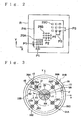
- Fig. 1(A) shows a composition of the projection exposure apparatus of this embodiment
- a KrF excimer laser light source (wave-length 248 nm) is used as an exposure light source 1.
- the laser light sources such as an ArF excimer laser light source (wave-length 193 nm), a F 2 laser light source (wave-length 157 nm), a Fr 2 laser light source (wave-length 146 nm), or an Ar 2 laser light source (wave-length 126 nm); or high frequency generating apparatus such as a high frequency generating light source of a YAGI laser or a solid laser (for example semiconductor laser etc.) can be used as a exposure light source 1.
- An illumination light L 1 comprised of ultraviolet pulse light as an optical beam for exposure (exposure beam) emitted from exposure light source 1 goes into the first diffractive optical element 21 through an optical path folding miller 3, after changing the cross-sectional shape of the optical beam into the desirable shape with beam expander 2, and is changed the optical beam DL which diffracts to the plural directions in order to be obtained a predetermined distribution of amount of light at a predetermined plane (for example pupil plane of the illumination system) as described after.
- the diffractive optical element 21 as a part of the optical member for setting distribution of amount of light is mounted to a revolver 24, the second diffractive optical element 22 having other diffractive characteristic and further, diffractive optical element (not shown) having another diffractive characteristic are also mounted.
- a main control system 17 controlling over the all operation of the apparatus controls the revolving angle of the revolver 24 through a driver 23, by setting one of the diffractive optical element 21 and 22 etc. on the optical path of the illumination light L 1, can change the condition of illumination.
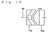
- the optical beam DL diffracted by the diffractive optical element 21 is gathered by a relay lens 4, is gathered on an incident plane of the fly' eye lens 5 as an optical integrator, through a first prism 71 and a second prism 72 (movable prism).
- the diffractive optical element 21 is arranged at a position slightly deviated from a front focus of the relay lens 4 to the exposure light source 1 than, and the incident plane of fly' eye lens 5 is approximately arranged at the position of the back focus of the relay lens 4.
- a plurality of optical beams diffracted to the different directions are respectively gathered at the different areas on the incident plane of the fly' eye lens 5, a plane light source (2-dimentional light source comprised of many light source images in this embodiment) of distribution approximately corresponding to the amount of light of the incident plane is formed.
- a combined lens system comprised of the relay lens 4 and fly' eye lens 5
- the exit plane of the diffractive optical element 21 and the exit plane Q 1 of the fly' eye lens 5 have approximately be conjugate (imaging relation).
- the diffractive optical element 21, the first prism 71, and the second prism 72 are corresponding to an optical member for setting a predetermined distribution of amount of light.
- the first prism 71 is a member which forms a parallel flat plate 71 at circular area of which the center is an optical axis BX (discuss later) of a illumination system, and forms a concave cone 71 b around the circular area;
- the second prism 72 is a member which forms inverted concave and convex for the first prism 71, and forms a parallel flat plate as a whole by combining with the first prism 71.
- a optical beam passing the circular area of the center of the first prism 71 and the second prism 72 distributes to areas which are a center of a distribution of amount of light on the exit plane Q1 on the fly' eye lens 5 in which amount of light is enhanced;
- a optical beam passing the cone part (slope plane) around the first prism 71 and the second prism 72 distributes to a plurality of areas (or a predetermined area including the plurality of areas) in which amount of light is enhanced around the distribution of amount of light.
- the second prism 72 is only supported movably by a driving mechanism (not shown), thus by changing the distance between the first prism 71 and the second prism 72 by moving the second prism 72 along the optical axis BX, the position of a plurality of peripheral areas in which the amount of light is great can adjust to the radial direction, without changing the central distribution (position of areas 28, 33 etc. described bellow) of the distribution of amount of light at the exit plane Q1 on the fly' eye lens 5.
- a prism having not a cone but a pyramid may be used instead of the first prism 71 and the second prism 72. Furthermore, it is allow moving this position along the optical axis BX by only using the first prism 71 instead of the first prism 71 and the second prism 72. Further, as shown Fig. 1(C) , it is allow using a pair of prisms 71A, 71B shaped like a letter V which has diffractive power to one direction and has not diffractive power to orthogonal direction, as the movable prism.
- each rectangle area (in this configuration, the parallel flat plate) of its center is approximately orthogonal to the optical axis BX and two slope planes of the around area are approximately symmetric with respect to a plane being orthogonal to the paper of Fig. 1(C) including the optical axis BX.
- another pair of prisms 71C, 71D constructed by revolving the pair of prisms 71A, 71B by 90 degrees about the optical axis BX may be arranged. Whereby, it is able to independently adjust each position (distance from the optical axis BX) being orthogonal each other in which amount of light is great.
- the prism described above whose slope plane is the cone, pyramid, or shaped like a letter V the center flat plate is the parallel flat plate, it may be aperture part (hollow part) by cutting at lest one part of the center part, or may be an integral solid by making a plurality of members independently. Inparticular, thelattermaybeanintegralsolid by only dividing the peripheral slope plate except the center flat plate part into a plurality of parts.
- the fly' eye lens 5 is, as an example, a bundle of many lens elements each of which has a rectangular cross-section whose vertical and horizontal width is about a few of millimeter, the shape cross-section of each lens element is approximately similar to a slim piece of illumination area on a reticle.
- a micro fly' eye lens constructed by binding many micro lenses whose shape cross-section is rectangular with about a few tens of micrometer or circular with diameter of about a few tens of micrometer can be used.
- the illumination light IL comprises optical beam emitted from the fly' eye lens 5 is onetime gathered on the plane Q2 by a condenser lens system 6.
- a fixed field stop (fixed blind) 7 for limiting an illumination area on a reticle R as an illuminated target to a slim shape orthogonal to scan direction, i.e., not-scan direction is arranged at slight front side of the plane Q2, a movable field stop (movable blind) 8 on the plane Q2.
- the movable field stop is used to prevent from useless exposure by controlling the width of the scan direction of the illumination area at the front and back of the scan exposure, and to limit the width of the not-scan direction of the illumination area during the scan exposure.
- a reticle stage driving system 16 described bellow controls open/close operation of the movable field stop 8 through a driving section 13 in sync with operation of the reticle stage.
- An illumination system 12 is composed of the exposure light source 1, a beam expander 2, the miller 3, the diffractive optical element 21 (or other diffractive optical element), the relay lens 4, fly' eye lens 5, the condenser lens system 6, field stop 7, 8, the imaging-lens system 9, the miller 10, and the main condenser lens system 11.
- An optical axis of the illumination system 12 is regarded as the optical axis BX.
- the exit plane Q1 of the fly' eye lens 5 is substantially coincident to an optical Fourier transform plane for the pupil plane of the illumination system 12, i.e., reticle: the plane Q2 in which the movable field stop 8 is arranged is a conjugate plane with the reticle plane.
- the fixed field stop 7, for example, may be arranged near the reticle plane.
- the imaging-circuit patterns within illumination area of the reticle R via a projection optical system PL of both side telecentrics as a projection system, transfers a resist layer of one shot area among a plurality of shot areas on a wafer W as a substrate arranged on an image-forming plane of the projection optical system PL with a predetermined downsizing magnification P (for example, ⁇ is 1/4, 1/5 etc.).
- a predetermined downsizing magnification P for example, ⁇ is 1/4, 1/5 etc.
- the reticle R and wafer W is respectively regarded as a first object and second object.
- the wafer W as substrate for exposure is a circular substrate such as semiconductor (silicon etc.) or SOI (silicon on insulator) whose diameter is 200 or 300 mm, for example.
- An optical axis AX of the projection optical system PL is coincident to an optical axis BX of the illumination system on the reticle R. Furthermore, a pupil plane Q3 (optical Fourier transform plane for the reticle plane) on the projection optical system PL is conjugate with the exit plane Q1 (the pupil plane of the illumination system 12) of the fly' eye lens 5.
- the projection optical system PL of this configuration other one except the diffractive system can be used, for example, a catadioptric projection optical system having a plurality of optical systems having optical cross-axes each other as disclosed in Japanese Patent Application: TOKUKAI 2000-47114 (corresponding to US Patent NO.
- a catadioptric projection optical system and the like which has an optical system including an optical axis intends from a reticle to a wafer and a catadioptric optical system including an optical axis being approximately orthogonal to that optical axis, and which forms an intermediate image twice in its interior as disclosed in international publication (WO): 01/065296 brochure (corresponding to US publication 2003/0011755A1 ).
- WO international publication
- 01/065296 brochure corresponding to US publication 2003/0011755A1 .
- the projection optical system PL with considering that a Z axis is paralleled to the optical axis AX, a X axis is not-scan direction (the direction parallel to the paper in Fig. 1(A) , in this case) orthogonal to the scan direction, and a Y axis is the scan direction (the direction orthogonal to the paper in Fig. 1(A) , in this case), as follows:
- the wafer W is adsorbed and held on a wafer stage 18 through wafer holder not shown; the wafer stage 18 is movably mounted in the X and Y directions on a wafer base 19.
- the position of the wafer stage 18 is measured by a laser interferometer in a wafer driving system 20.
- the wafer driving system 20 controls the position and velocity of the wafer stage 18 through driving mechanism not shown, based on the measured information and control information from the main control system 17.
- a focusing mechanism for fitting the surface of the wafer into the image-forming plane of the projection optical system PL is assembled in the wafer stage 18 during the scan exposure, based on measured information of an auto-focus sensor not shown.
- Fig. 2 shows an example of a pattern (original pattern) for transferring formed on a reticle R; in Fig. 2 , a 2-dimentional pattern with three kinds of contact holes arranging pattern 25A, 25B, and 25C of approximate squares with pitch P1, P2, and P3 at the X, Y directions in a pattern region PA of the reticle R.
- Each pattern 25A, 25B, and 25C may be a transmission pattern formed in a light shielded film, or may conversely be a light shielded pattern formed in a transmission part.
- each pattern 25A, 25B, and 25C is around equal to 1/2 or smaller than corresponding pitch P1, P2, and P3 respectively, however, the width of pattern 25B, 25C with larger pitch can be around equal to pattern 25A with most fine pitch.
- the pitch P1, P2, and P3 are set to gradually become several-fold, as follows: P ⁇ 1 ⁇ P ⁇ 2 ⁇ P ⁇ 3
- the projection magnification ⁇ of the projection optical system PL in Fig. 1 (A) is 1/4-fold
- pitch P1, P2, and P3 on the reticle plane are respectively set, as an example, around 300 nm, 600 nm, and 900 nm. That is, the original patterns on the reticle plane include a first pattern for dense contact holes with fine pitch, a second pattern for dense contact holes with around middle pitch, and a third pattern for contact holes arranged with large pitch substantially regarding as the isolated contact holes. In order to transfer an image of these original patterns on wafer onetime with high accuracy, as shown Fig.
- the diffractive optical element 21 on the optical path of an illumination light IL, the distribution of amount of light (strength distribution) of the illumination light IL at the exit plane Q1 (pupil plane) of the fly' eye lens 5 as a predetermined plane.
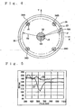
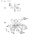
- Fig. 3 shows the distribution of amount of light of the illumination light IL at the exit plane Q1 (pupil plane of the illumination system) of the fly' eye lens 5.
- the direction on the exit plane Q1 corresponding to the X direction and Y direction (i.e., the arranging direction of the pattern to transfer) on the reticle R is respectively defined the X direction and Y direction.
- NA the numerical aperture of the object side (reticle side) of the projection optical system PL in Fig. 1(A)
- NA PL the numerical aperture of the image side (wafer side)
- the maximum value among the numerical apertures of the illumination light IL incident to the reticle R from the illumination system 12 is NA IL
- the value of ratio (coherence factor) of the maximum numerical aperture NA IL to the numerical aperture NA of the projection optical system PL is called maximum ⁇ value in this embodiment
- maximum ⁇ value is ⁇ . That is, the illumination light of maximum ⁇ value is the light incident on the reticle R with the maximum angle among the illumination light IL.
- a maximum outer circle 26 indicates an outer area passed through virtual optical beam having the same numerical aperture as the numerical aperture NA at the incident side of the projection optical system PL
- an inner circle 27 indicates a circle is tangent to areas passed through illumination light having numerical aperture of the maximum ⁇ value ( ⁇ ) ; all illumination light pass though within the circle 27.
- 3 approximately has a constant amount of light at nine areas with distance each other which include a circular area 28 with radius r1 centered an optical axis BX of the illumination system 12, four circular areas 29A, 29B, 29C, and 29D with radius r2 whose centers are arranged along a first circle 32Awith radius R1 enclosing the area 28, and four circular areas 30A, 30B, 30C, and 30D with radius r3 whose centers are arranged along a second circle 32B with radius R2 enclosing the areas 29A to 29D, and has distribution of amount of light of lower amount of light (approximate 0 in this embodiment) at other areas than the constant amount of light.
- the amount of light, near the outline of the area 28, areas 29A to 29D, and areas 30A to 30D may have distributions which gradually decrease toward the outside.
- the center area 28 corresponds to a first area; the four areas 29A to 29D enclosing the area 28 correspond to second areas; further the four areas 30A to 30D enclosing the areas 29A to 29D correspond to third areas.
- the radii r1 to r3 and R1, R2 respectively indicates the length (distance between point passed through the optical beam of the maximum ⁇ value and the optical axis BX) corresponding the maximum ⁇ value ( ⁇ ) as unit.
- the center area 28 is set larger than other eight areas 29A to 29D and 30A to 30D (r1 > r2 > r3). Further, since the arranging directions of the 2-dimentional patterns as the targets to transfer are the X direction and Y direction, it is defined that a straight line crossed to the X direction by 45 degrees in clock winding is a straight line 31A; a straight line (the straight line crossed to the X direction by 45 degrees in counter clock winding) is a straight line 31B.
- the center of the center area 28, the middle two areas 29A and 29C, and other most outer two areas 30A and 30C is arranged on the first straight line 31A; the center of the center area 28, the middle other two areas 29B and 29D, and other most outer two areas 30B and 30D is arranged on the second straight line 31B. That is, the eight areas 29A to 29D and 30A to 30D enclosing the center area 28 are arranged along the two directions being orthogonal with revolving the two arranging directions by 45 degrees, which are orthogonal, in which patterns as the targets for transfer.
- the diffractive characteristic of the diffractive optical element 21 in Fig. 1(A) is set, so as to obtain the distribution of amount of light in which the amount of light approximately becomes constant at the area 28, the areas 29A to 29D, and the areas 30A to 30D in Fig. 3 satisfying the condition of the equations (7) to (10): approximately becomes 0 at other areas.
- the diffractive optical element 21, as an example can fabricate by forming a concave and convex grating having approximately systematically along in the direction of the straight line 31A, and a concave and convex grating having approximately systematically along in the direction of the straight line 31B of Fig. 3 .
- the diffractive optical element 21 may be a combination of a plurality of phase type diffractive gratings.
- the diffractive optical element 21 is phase type, it is advantage of high efficiency for using light.
- it is able to use an optical element changing refractive index distribution corresponding to a diffractive grating distribution as an optical element 21.
- a construction and a method for fabricating having a specific diffractive characteristic is closely disclosed, for example, in Japanese Patent Application: TOKUKAI 2001-176766 (corresponding to US Patent NO. 6,563,576 ) by this applicant.
- the aperture stop whose aperture is formed at the part corresponding to the area 28, the areas 29A to 29D, and the areas 30A to 30D in Fig. 3 , may be arranged at the exit plane Q1 (pupil plane) of the fly' eye lens 5 for its conjugate plane. Also in this case, it is advantage of high efficiency for using the illumination light L1.
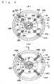
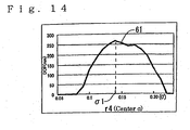
- this inventor have evaluated the CD (critical dimension), through the simulation of the computer, which is obtained by transferring a downsizing image of pattern of contact holes with various kinds of pith arranged on the reticle plane to the wafer through the projection optical system PL, under the distribution of amount of light in which the amount of light becomes constant at the nine areas comprising the area 28, the areas 29A to 29D, and the areas 30A to 30D in Fig. 3 satisfying the condition of the equations (7) to (10) : becomes 0 at the other areas.
- the CD used is the line width of patterns transferred.
- the numerical aperture NA PL of the image side (wafer side) of the projection optical system PL in Fig. 1(A) is 0.82
- projection magnification ⁇ is 1/4-fold
- the curve 36 in Fig. 5 shows the simulation result of the CD value in case that the amount of light becomes constant at the nine areas on the pupil plane, the horizontal axis is the pitch (nm) of the pattern transferred on the reticle plane, vertical axis is the CD value (nm) in Fig. 5 .
- the pitch 280 to 1120 nm is equivalent of 70 to 280 nm at the wafer side.
- the preferable CD value having approximately constant across the wide range of pitch 280 to 1120 nm.
- the patterns of the reticle R including three kinds of pitch in Fig. 2 can onetime transfer on the wafer with high accuracy.
- the radius r1 of the area 28, the radii r2 of the areas 29A to 29D, and the radii r2 of the areas 30A to 30D may be the ranges, as follows: 0.2 ⁇ ⁇ ⁇ r ⁇ 1 ⁇ 0.4 ⁇ ⁇ 0.75 ⁇ ⁇ ⁇ r ⁇ 2 ⁇ 0.2 ⁇ ⁇ 0.75 ⁇ ⁇ ⁇ r ⁇ 3 ⁇ 0.2 ⁇ ⁇
- the radius R1 of the first circle 32A and the radius R2 of the second circle 32B may be changed up to around +10% of the equations (9) and (10).
- the numerical aperture NA PL of the image side, the projection magnification ⁇ , and the maximum ⁇ value ( ⁇ ) in the projection optical system PL can be taken any values though the values described above.
- the maximum ⁇ value ( ⁇ ) by changing the distance between prism 71 and 72 in Fig. 1(A) , the radial position of the areas 29A to 29D, and the areas 30A to 30D with peripheral area in which the amount of light is great among the distribution of amount of light in Fig.
- Fig. 3 (the distance from the optical axis BX relating to the X direction and Y direction) may only be changed.
- Fig. 1(C) by using two pairs of prism 71A, 71B and 71C, 71D, the position of the areas 29A to 29D, and the areas 30A to 30D with peripheral area in which the amount of light is great among the distribution of amount of light in Fig. 3 (the distance from the optical axis BX) in the X direction and Y direction may independently controlled.
- the amount of light of the center area 28 e.g., intensity per unit size
- the amount of light of the four areas 29A to 29D along the peripheral first circle 32A and that of the four areas 30A to 30D along the peripheral second circle 32B may be different.
- the relative amount of these lights may be adjusted so that the optimum resolution is obtained for each pattern, for example.
- a distribution of amount of light becoming great amount of light of the five areas including four slim areas 130A, 130B, 130C, and 130D which are substantially connected to the radial each two areas 29A, 29B, 29C, 29D, 30A, 30B, 30C, and 30D of the radial in Fig. 3 respectively and the center area 28 may be used. Also in this case, it is almost able to transfer patterns having various kinds of pitch with high resolution.
- the amount of light of the connecting parts of two areas in the radial may around equal to that of the two areas, or may be different from that of the two areas, for example smaller.
- annular may be used instead of the center area 28 as the first area.
- Fig. 6(A) shows a distribution of amount of light of the illumination light IL on the exit plane Q1 (pupil plane of the illumination system 12) of fly' eye lens 5 in Fig. 1(A) , when the first area is the area of annular.
- the amount of light of the area 28R of annular consist of the outer radius r1, the inner radius rlR, and the center of the optical axis BX and that of the nine areas including the area 28, the areas 29A to 29D, and the areas 30A to 30D are approximately constant; and amount of light of the illumination light at the other areas is approximately 0.
- the condition other than it is the same as that of the case where the amount of light in Fig. 3 is used.
- the light distributed at the peripheral areas 29A to 29D, and the areas 30A to 30D in Fig. 6(A) may be linear polarization.
- the light distributed at the peripheral areas may be S polarization (vertical direction for the incident plane) whose polarization direction is the tangent direction.
- S polarization vertical direction for the incident plane
- the resolution etc. for the specific pattern might be enhanced. It is the similar to the case of using the distribution of amount of light in Fig. 3 or 6(B) .
- the optical beam is preferably changed into that of the linear polarization whose polarization direction is approximately coincident to the circumference direction.
- the polarization setting member is preferably arranged between one of the plurality of prisms (movable member) described above which is arranged at the most upstream side (light source side) and incident side, for example the lens 4, or the diffractive optical element 21 and the lens4.
- the center circular area 28 may be the area of the annular similar to Fig. 6(A) .
- the diffractive optical element 21 in this embodiment sets the distribution of amount of light on the pupil plane of the illumination system 12 as a predetermined plane to a predetermined state; the predetermined plane may be the pupil plane Q3 of the projection optical system PL.
- the distribution of amount of light is set which is approximately constant at the first area including the axis AX and the eight areas enclosing it, and which is lower at the other areas.
- the area 28 (or 28R), each of the areas 29A to 29D, and the areas 30A to 30D, in which amount of light is approximately constant on the pupil plane is the circular (or annular) however, each circular (or annular) can be an area of ellipse (ellipse annular).
- the area of circular (or annular) can be an area of polygon (or frame shape of polygon), or can be combination of the area of circular (or annular) and the area of polygon.
- Fig. 9 shows possible another distribution of amount of light on the pupil plane, as shown Fig. 9 , the distribution of amount of light is approximately constant at the center square (right square or right hexagon etc. is possible) area 28A, four square areas 30E to 30 H enclosing it, and lower than it at the other areas.
- the positions and sizes of the areas may be respectively similar to those of the area 28, areas 29A to 29D, and the areas 30A to 30D.
- an area of frame type may be used instead of the center area 28A in Fig. 9 .
- a second diffractive optical element 22 having different diffractive characteristic is provided to the revolver 24 in Fig. 1(A) .
- the second diffractive optical element 22 With setting the second diffractive optical element 22 on the optical path of the illumination light IL, distribution of amount of light which is approximate constant amount of light at the five areas of the exit plane Q1 (pupil plane) of the fly-eye lens 5, and the lower (approximate 0 in this embodiment) than it at the other area is obtained.
- Fig. 7(A) shows a distribution of amount of light of the illumination light IL on the exit plane Q1 (pupil plane) of fly-eye lens 5 in Fig. 1(A) , when the second diffractive optical element 22 is used.
- Fig. 7 (A) with marking the same notes to the parts corresponding to in Fig.
- the distribution of amount of light at five areas with distance each other including an area 33R (first area) of circular annular consist of the outer radius r1, the inner radius r1R, and the center of the optical axis BX of the illumination system 12, and four circular areas 34A, 34B, 35C, and 35D (second area) arranging along the a circle 35 having radius R3 with radius r5 and 90 degrees distance enclosing the area 33R is approximately constant; and is smaller (approximate 0 in this configuration) than the constant amount of light.
- the outer outline of the center area 33R is set larger than that of other four areas 34A to 34D (r4>r5).
- the preferable range of the radius r4 is similar to that of the radius r1 of the equation (13), and the preferable range of the radius R3 and radius r5 are similar to that of the radius R2 of the equation (10) and radius r2 of the equation (14) respectively.
- the outer four areas 34A to 34D are respectively arranged along the straight lines pass through the optimal axis BX and cross by 45 degrees in the X direction (or Y direction).
- This inventor has evaluated the CD (critical dimension), through the simulation of the computer, which is obtained by transferring a downsizing image of pattern of contact holes with various kinds of pith arranged on the reticle plane to the wafer through the projection optical system PL, under the distribution of amount of light in which the amount of light becomes constant at the five areas comprising the area 33, and the areas 34A to 34D in Fig. 4 satisfying the condition of the equations (16) and (17) ; becomes 0 at the areas in addition thereto.
- the exposure wave length is ArF laser light
- the numerical aperture NA PL of the image side (wafer side) of the projection optical system PL in Fig. 1(A) is 0.78
- projection magnification ⁇ is 1/4-fold
- the maximum ⁇ value ( ⁇ ) is 0.9.
- the curves of line graph F1, F2 in Fig. 8 show the simulation result of the CD value in case that the amount of light becomes constant at the five areas on the pupil plane, the horizontal axis is the defocus amount of wafer ( ⁇ m), vertical axis is the line width ( ⁇ m) (line width on wafer) of the pattern well transferredas the CDvalue. Furthermore, approximate flat curve F1 indicates simulation result for the pattern of contact holes with line width 140 nm, pitch 220; mountain-shaped curve F2 indicates simulation result for the isolated pattern with line width 140 nm. As shown F1, F2, approximately constant CD value with range in which the defocus amount is around -0.2 ⁇ m to 0.2 ⁇ m is obtained. Accordingly, various kinds of pattern from the isolated pattern to the pattern with fine contact holes with high accuracy and wide depth of focus.
- Fig. 7 (A) when the distribution of amount of light in Fig. 7 (A) is used, for example, in order to control the maximum ⁇ value ( ⁇ ), by changing the distance between prisms 71 and 72 in Fig. 1(A) , the radial position (distance from the optical axis BX relating to the X direction and Y direction) of the areas 34A to 34D in which the amount of light is great in Fig. 7(A) may be changed.
- Fig. 7 (A) in order to control the maximum ⁇ value ( ⁇ )
- Fig. 7(A) it can be set the amount of light of the center area 33R (e.g., intensity per unit size) and that of the peripheral four areas 34A to 34D differ.
- the relative amount of these lights may be adjusted so as to be obtained the optimum resolution at each pattern for example.
- a distribution of amount of light becoming great amount of light of the area 134 which is a starfish shape having an aperture at the center or a star shape substantially connected the four areas 34A to 34D and the center annular zone area 33R in the radial direction may be used.
- the amount of light of the central part of the area 134 may be not 0 only smaller. Also in this case, it is almost able to transfer patterns having various kinds of pitch with high resolution.
- the amount of light of the connected part getting longer to radial direction may be around equal to those of the peripheral and center areas, or may be different from those, for example smaller than those.
- the light distributed at the peripheral areas 34A to 34D in Fig. 7 (A) maybe linear polarization.
- the light distributed at the peripheral areas maybe S polarization (vertical direction for the incident plane) whose polarization direction is the tangent direction.
- the resolution etc. for the specific pattern might be enhanced. It is the similar to the case of using the distribution of amount of light in Fig. 7(B) .
- the light distributing the peripheral area getting longer to the radial direction, particularly its part corresponding to the peripheral areas 34A to 34D in Fig. 7 (A) may be the linear polarization whose polarization becomes the tangent direction.
- the light distributed at the peripheral areas is non-polarization or whose polarization direction is not coincidental to the circumference direction, as described above, for example, it is preferable to provide polarization setting member between the diffractive optical element 21 and the fly-eye lens 5.
- Fig. 4 shows the distribution of amount of light in which the amount of light is set constant at a circular area 33 instead of the center annular zone area 33R in Fig. 7(A) , and the amount of light is set constant at four areas 34A to 34D enclosing it as with Fig. 7(A) .
- This inventor have evaluated the CD (critical dimension), through the simulation of the computer, which is obtained by transferring a downsizing image of pattern of contact holes with various kinds of pith arranged on the reticle plane to the wafer through the projection optical system PL, under the distribution of amount of light in which the amount of light becomes constant at the five areas comprising the area 33, and the areas 34A to 34D in Fig. 4 satisfying the condition of the equations (18) and (19): becomes 0 at the other areas.
- the values of the numerical aperture NA PL of the image side (wafer side) of the projection optical system PL in Fig. 1(A) , projection magnification ⁇ , and the maximum ⁇ value ( ⁇ ) are similar to the equation (12) in the Fig. 3 .
- the dotted line curve 37 in Fig. 5 shows the simulation result of CD value in which the amount of light becomes constant at the five areas of this pupil plane, as shown in the curve 37; the CD value is low around pitch 500 to 700 nm.
- the second configuration will be described accompanying Fig. 10 to Fig. 17 .
- the exposure is fundamentally performed by using the scan exposure type projection optical apparatus in Fig. 1(A) .
- a diffractive optical element 22A (described bellow in detail) having different characteristic is used instead of the diffractive optical element 21 in Fig. 1(A) .
- the diffractive optical element 22A, the first prism 71, and the second prism 72 are corresponding to an optical member for setting a predetermined distribution of amount of light.
- the prism 71, 72 (or the first prism 71 only) are used as movable prism.
- Fig. 10 it is allow using a pair of prisms 71A, 71B shaped like a letter V which has diffractive power to one direction and has not diffractive power to orthogonal direction, as the movable prism.
- the prisms 71A, 71B are arranged so that each rectangle area (in this configuration, the parallel flat plate) of its center is approximately orthogonal to the optical axis BX and two slope planes of the around area are approximately symmetric with respect to a plane being orthogonal to the paper of Fig. 1(A) including the optical axis BX.
- a reticle RA is loaded on the reticle stage 14 instead of the reticle R in Fig. 1(A) .
- Fig. 11(A) shows an example of a pattern (original pattern) for transferring formed on the reticle RA loaded on the reticle stage 14 in Fig. 1(A) .
- a pattern 52 for the one directional high density pattern is formed, in which square aperture patterns 51 having width a in the X direction and width b in the Y direction, are periodically arranged in the X direction (non-scan direction in this configuration) with pitch P at the pattern region PA.
- the pitch P is fine pitch (for example, around 150 nm length converted to projection image on wafer W) which is close to approximate limited resolution of the projection exposure apparatus in this configuration, the width a of the X direction is around 1/2 of the pitch P, and the width b of the Y direction is around equal to the width a to 10-fold (around a to 10a).
- the pattern 52 is one directional high density pattern which can regard an isolated pattern about the Y direction (scan direction in this configuration).
- the pattern 52 is the periodical pattern arranging four aperture pattern 51 in X direction, the number of the aperture pattern 51 may be 2 or any than 2.
- the aperture pattern 51 is the transmission pattern formed in a light shielded film, a light shielded pattern provided in transmission part may be used instead of it.
- another pattern 53 for one directional high density pattern is also formed at a position distant from the pattern 52 in the Y direction, in which square aperture patterns 51 with pitch Q larger than the pitch P.
- the pattern 52 and 53 are actually small pattern whose length of X direction is a few ⁇ m or less, various kinds of other pattern (not shown) may be formed on the pattern region PA of the reticle RA.
- each of pattern 52A, 52B, and 52C is regarded as one directional high density pattern, can be the target for transfer in this configuration.
- the plurality of periodic pattern may only be arranged with the distance, so as to be isolated for orthogonal direction (Y direction) to the periodic direction, and their number may be arbitrary.
- Fig. 1(A) In order to transfer image of these original patterns on wafer with high accuracy, as shown Fig. 1(A) in this configuration, with arranging the diffractive optical element 22A on the optical path of an illumination light IL, the distribution of amount of light (strength distribution) of the illumination light IL at the exit plane Q1 (pupil plane) of the fly-eye lens 5 as a predetermined plane.
- Fig. 12 shows the distribution of amount of light of the illumination light IL at the exit plane Q1 (pupil plane of the illumination system 12) of the fly-eye lens 5 in Fig. 1 in this embodiment.
- the direction on the exit plane Q1 corresponding to the X direction (periodically arranging direction) and Y direction (regarding as isolated direction) on the reticle R is respectively defined the X direction and Y direction.
- NA the numerical aperture of the object side (reticle side) of the projection optical system PL in Fig. 1(A)
- NA PL the numerical aperture of the image side (wafer side)
- the maximum value among the numerical apertures of the illumination light IL incident to the reticle R from the illumination system 12 is NA IL
- the value of ratio (coherence factor) of the maximum numerical aperture NA IL to the numerical aperture NA of the projection optical system PL is called maximum ⁇ value in this embodiment
- maximum ⁇ value is ⁇ IL . That is, the illumination light of maximum ⁇ value is the light incident on the reticle R with the maximum angle among the illumination light IL.
- a maximum outer circle 26 indicates an outer area passed through virtual optical beam having the same numerical aperture as the numerical aperture NA at the incident side of the projection optical system PL
- an inner circle 27 indicates a circle is tangent to areas passed through illumination light having numerical aperture of the maximum ⁇ value ( ⁇ IL ); all illumination light pass though within the circle 27.
- the illumination light IL in Fig. 12 , has the distribution of amount of light with the approximate constant amount of light at the three areas (hatched areas) including the annular zone area 54 with the radius r4 which centers on the optical axis BX of the illumination system 12 and the two circular areas 55A, 55B with the radius r5 sandwiching the area 54 in the X direction; and with the smaller amount of light (approximate 0 in this configuration) than the constant amount of light.
- the centers of the three areas 54, 55A, and 55B are arranged along the straight line which passes through the optical axis of the illumination system and parallels the X axis (periodically arranging direction of one directional high density pattern as target for transfer), the distance between the each center of the area 55A and 55B both ends and the optical axis BX is respectively R3.
- the annular zone area 54 has 1/2 annular in which the inner radius is 1/2 of the outer radius r4, 1/3 annular in which the inner radius is 1/3 of the outer radius r4, or 2/3 annular in which the inner radius is 2/3 of the outer radius r4 and the like.
- the circular area 54A with the radius r4 can be used instead of the annular zone area 54.
- a plurality of areas substantially split can be used instead of the annular zone area 54. Concretely, as shown in Fig.
- the distribution of amount of light at the two half-circular (or circular etc.) areas 54A1, 54A2 split in the Y direction (or X direction), in which the amount of light become great, may be used instead of the annular zone area 54.
- the amount of light may become great at a four-way split area in the X direction and Y direction (or direction crossed these axes) instead of the annular zone area 54.
- distribution in which the amount of light gradually decreases toward outer may be near the outline of the area 54, 55A, 55B.
- the center area 54 is corresponding to the first area, and the two areas 54A and 54B sandwiching it is respectively corresponding to the second area and third area.
- the radii r4, r5 and R3 respectively indicate the radius ⁇ in the equation (6B) (distance between point passed through the optical beam of the maximum ⁇ value and the optical axis BX) corresponding to the maximum ⁇ value ( ⁇ IL ) as unit.
- the radii r4, r5 are preferably set within around 0.1 ⁇ to 0.2 ⁇ respectively, as follows: 0.1 ⁇ ⁇ ⁇ r ⁇ 4 ⁇ 0.2 ⁇ ⁇ 0.1 ⁇ ⁇ ⁇ r ⁇ 5 ⁇ 0.2 ⁇ ⁇
- radius r4 and radius r5 are preferably equal, as follows: r ⁇ 4 ⁇ r ⁇ 5 ⁇
- the diffractive characteristic of the diffractive optical element 21 in Fig. 1(A) is set, so as to obtain the distribution of amount of light in which the amount of light approximately becomes constant at the area 54, the areas 55A, 55B in Fig. 12 satisfying the condition of the equations (21) to (24); approximately becomes 0 at other areas.
- the diffractive optical element 22A as an example, can fabricate by forming a concave and convex grating having approximately systematically along in the direction of the straight line 31A, and a concave and convex grating having approximately systematically along the X axis of Fig. 12 .
- the diffractive optical element 22A may be a combination of a plurality of phase type diffractive gratings.
- the diffractive optical element 22A is phase type, it is advantage of high efficiency for using light.
- it is able to use an optical element changing refractive index distribution corresponding to a diffractive grating distribution as an optical element 22A.
- a construction and a method for fabricating having a specific diffractive characteristic is closely disclosed, for example, in Japanese Patent Application Laid-open No. 2001-176766 (corresponding to US Patent NO. 6,563,567 ) by this applicant.
- the amount of light distribution obtained by diffraction optical device 22A is set to be approximately the predetermined of light at a region including regions 54, 55A and 55B in Fig. 12 .
- an aperture stop where an aperture is formed at a portion corresponding to the regions 54, 55A and 55B in Fig. 12 may be disposed on the emission plane Q1 (pupil plane) of the fly eye lens 5 in Fig. 1(A) . Also in this case, advantage in which utilization efficiency of the illumination light IL is high is obtained.
- Fig. 13(A) shows diffraction light (focus light flux) diffracted in the isolated Y direction from the pattern 52.
- Fig. 13(B) shows diffraction light (focus light flux) diffracted in the periodic X direction from the pattern 52.
- light beams 58, 59 and 60 show the illumination light IL passed through the regions 54, 55A and 55B on the pupil plane of the illumination system in Fig. 12 respectively.
- the diffraction light generated from the pattern 52 (aperture pattern 51) due to the light beams 58, 59 and 60 generates, in the Y direction, with distribution in which the diffraction light is generated most strongly at the center, and the larger the tilt angle, the lower the intensity decreases, as shown in Fig. 13 (A) .
- the pattern 52 of this embodiment is approximately the resolution limit, therefore, the positive primary light 59P from the pattern 52 due to one light beam 59 is made incident into the projection optical system PL in Fig. 1(A) in parallel to the other zero-order light 60, while, the negative primary light 60M from the pattern 52 due to the other light beam 60 is made incident into the projection optical system PL in Fig. 1(A) in parallel to one zero-order light 59.
- wavelengths of incident light beams 58, 59 and 60 are taken to as ⁇
- exit angle in the X direction to the normal line of the pattern 52 of the zero-order light 59 is taken to as ⁇
- exit angle in the X direction to the normal line of the pattern 52 of the zero-order light 60 is taken to as - ⁇
- Fig. 13(B) among the other light beams 59, the light beampassed through the adjacent aperture pattern 51 with interval P of the X direction is taken to as the light beams 59A and 59B.
- equation (26) corresponds to the case in which focal distance fQ1 at the side of the emission plane Q1 of the partial optical system between the emission plane Q1 (pupil plane) in the illumination system 12 in Fig. 1A and the reticle plane is set to 1.
- Equation (26) corresponds to the case in which focal distance fQ1 at the side of the emission plane Q1 of the partial optical system between the emission plane Q1 (pupil plane) in the illumination system 12 in Fig. 1A and the reticle plane is set to 1.
- equation (27A) indicates resolution limit of X direction (cycle direction) in the object plane (reticle plane) of the projection exposure apparatus of this embodiment, in which the larger is the interval R3 while making ⁇ larger or while making radius r5 smaller, the less it is possible to make the pitch P to be the resolution limit smaller.
- the pitch P is converted into pitch ⁇ P as the following equation, which the pitch ⁇ ⁇ P is length on the wafer.
- the pitch ⁇ P becomes the resolution limit in the X direction on the image plane (wafer plane) of the projection optical system PL.
- ⁇ ⁇ P ⁇ ⁇ ⁇ / 2 ⁇ ⁇ - r ⁇ 5
- the wavelength ⁇ is set to 193.306 nm.
- numerical aperture NA PL at the wafer side of the projection optical system PL is taken to be 0.85
- projection scale factor ⁇ of the projection optical system PL is taken to be 1/4
- ⁇ IL to be ⁇ value of illumination system 12 is taken to be 0.90
- radius r5 of the regions 55A and 55B in Fig. 12 is taken to be 0.14 ⁇ , that is called as "the first illumination condition”.
- the resolution limit ⁇ P at the image plane side under this condition becomes about 147 nm as shown in next equation from relationship of the equations (6B) and (27B).
- ⁇ ⁇ P 146.7 nm
- Fig. 12 can be regarded as the drawing showing amount of light distribution in the X direction in the pupil plane Q3 of the projection optical system PL in Fig. 1(A) .
- the regions 54, 55A and 55B in Fig. 12 correspond to position through which the zero-order light of the illumination light IL is passed, and the positive primary light in the X direction of the illumination light IL according to the pattern 52 in Fig.
- 11(A) becomes distribution in which the amount of light distribution in the circumference 27 is moved in parallel toward the region in the circumference 57A with the spaced point 56A as the center, which the spaced point 56A is spaced from the optical axis BX (optical axis AX of the projection optical system PL) by only interval 2 ⁇ R3 in the +X direction.
- the negative primary light in the X direction of the illumination light IL according to the pattern 52 becomes distribution in which the amount of light distribution in the circumference 27 is moved in parallel toward the region in the circumference 57B with the spaced point 56A as the center, which the spaced point 56B is spaced from the optical axis BX (optical axis AX) by only interval 2 ⁇ R3 in the -X direction.
- the positive primary light (or the negative primary light) of the light beam passing through the region 55B (or 55A) passes through the region 55A (or 55B), therefore, the image of the pattern 52 is projected on the wafer with high resolution.
- the present inventor in order to obtain the optimum balance between radius r4 of central region 54 and radius r5 of the regions 55A and 55B at both ends in Fig. 12 , has calculated depth of focus (DOF) of the image according to the projection optical system PL with simulation of the computer while varying the radius r4 gradually.
- the condition in addition to the r4, at this time, is the same as the above described first illumination condition, and the radius r5 is 0.14 ⁇ .
- the pitch P of the pattern 52 in Fig.
- the pitch P, and the widths a and b are lengths which are converted on the image plane of the projection optical system PL respectively.
- the curved line 61 in Fig. 14 shows the simulation results, and the horizontal axis in Fig. 14 is the radius r4 (unit is ⁇ ) of the region 54 (center ⁇ ) of the center of Fig. 12 , and the vertical axis is calculation results of the depth of focus (DOF) (nm) corresponding to the value of the radius r4.
- DOF depth of focus
- pattern 53 of the one directional high density contact hole existing in the position spaced from the pattern 52 of Fig. 11(A) arrangement direction is the same as that of the pattern 52, and the pitch Q is larger than the pitch P, therefore, the pattern 53 is transferred on the wafer with high resolution under the above described illumination condition.
- the pattern of the reticle RA including the pattern 52 of the one directional high density contact hole of Fig. 11(A) is capable of being transferred on the wafer W in the X direction and the Y direction with high resolution.
- At least one of 2 regions 55A and 55B except for the central region 54 is allowed that distance of the optical axis BX concerning the direction in parallel to the cyclic direction of the other pattern is not zero, or the distance is allowed to be set in accordance with the pitch of the other pattern, for instance.
- numerical aperture NA PL at the image side of the projection optical system PL, the projection scale factor ⁇ , and the maximum ⁇ value ( ⁇ IL) of the illumination system 12 are capable of taking arbitrary value without restricting the value to the above described values.
- position (distance of the optical axis BX concerning X direction to the region 55B) in the radius direction of the regions 55A and 55B where peripheral amount of light is large among amount of light distribution of Fig. 12 is allowed to be varied while varying interval between prisms 71 and 72 of Fig. 1(A) to control the maximum ⁇ value ( ⁇ IL), or the interval R3 of Fig. 12 .
- the amount of light (for instance, intensity per unit area) of the center region 54 is made different from the amount of light of peripheral 2 regions 55A and 55B. Relative largeness of these light quantities is allowed to be adjusted so that the optimum resolution can be obtained every transferring pattern, for instance.
- distributed light in peripheral regions 55A and 55B of Fig. 12 may be made linearly polarized light.
- the light distributed on the peripheral regions 55A and 55B is made S polarization in which the polarizing direction is direction of the tangential line (vertical direction to incident plane).
- the lights which are respectively distributed at three regions having large peripheral amount of light described above while being generated from the light source 1 are non-polarized lights, or the polarizing direction thereof do not agree with the direction of the tangential line
- the lights are converted into the light beam of the linear polarized light in which the polarizing direction approximately agrees with the direction of the tangential line upon disposing the polarization setting member such as a half-wave plate or a quarter-wave plate or so forth on the optical path through which the lights distributed at respective regions are passed between the diffraction optical device 21 (deflection member) and the fly eye lens 5, for instance.
- the polarization setting member at incident side of one prism (movable member), which is movable along the optical axis BX and disposed at the most upstream (light source side) between one pair of the prisms described above, for instance, between the movable member and the lens 4, or between the diffraction optical device described above and the lens 4.
- the polarization setting member it is not necessary to move the polarization setting member in accordance with variation of direction of travel of the light beam (optical path) caused by exchange of the diffraction optical device or interval change of one pair of prisms or so forth, or it is not necessary to form the polarization setting member largely in anticipation of its variation.
- the diffraction optical device 22A in this configuration sets the amount of light distribution on the pupil plane of the illumination system 12 as the predetermined plane into predetermined condition, however, the predetermined plane is possible to be the pupil plane Q3 of the projection optical system PL of Fig. 1(A) .
- the amount of light distribution which becomes approximately constant in the first region including the optical axis AX and in two regions putting the first region therebetween, and becomes lower amount of light than it at the region in addition thereto, is set in the pupil plane Q3 of the projection optical system PL.
- the regions 54, 55A and 55B which have approximately constant amount of light on the pupil plane, have circular form (or annular form), however, outward form of those regions are possible to be respective oval regions. Further, outward form of each region is possible to be rectangular region as described later, furthermore, outward form of each region is possible to be combined between the circular (or oval) region and the rectangular region.
- Fig. 15(B) shows another possible amount of light distribution on its pupil plane, as shown in Fig. 15(B) , the amount of light distribution becomes approximately the predetermined of light at the frame shaped region 54B of the center rectangular shape (regular hexagon or so forth is possible in addition to square), and at two rectangular regions 55C and 55D, which put the region 54B therebetween in the X direction, and the amount of light distribution becomes low at the region in addition thereto.
- position and area of the rectangular (or frame shape) region are allowed to be approximately the same as the position and area of the regions 54, 55A and 55B of Fig. 12 .
- the second diffraction optical device 22B When the second diffraction optical device 22B is mounted on the optical path of the illumination light IL, there is obtained the amount of light distribution, which becomes approximately the predetermined of light at three regions 62, 63A and 63B of Fig. 16(A) , and becomes the amount of light lower than it (approximate zero in this embodiment) in the region in addition thereto, at the emission plane Q1 (pupil plane) of the fly eye lens 5.
- Fig. 16(A) shows the amount of light distribution of the illumination light IL in the emission plane Q1 (the pupil plane of the illumination system 12) of the fly eye lens 5 in Fig. 1(A) in the case that the second diffraction optical device 22B is used.
- Fig. 16(A) where the same sign is added to corresponding part to Fig.
- oval regions 63A and 63B (the second region and the third region) having the shape in which slender in the Y direction is external form, width in the X direction is t, and length in the Y direction is h (h>t), so as to put the circular region 62 (the first region) of the radius r6 between these two oval regions 63A and 63B in the X direction, with the optical axis BX of the illumination system 12 in Fig. 1(A) as the center, so that the interval from the optical axis BX to each center becomes R4.
- the center region 62 is allowed to be the annular shape.
- Two slender oval regions 63A and 63B are the overlapped region in which the region in the circumference 27 having the radius ⁇ is overlapped by the region in the circumferences 65A and 65B whose radii are NA (or ⁇ is possible) by employing the positions 64A and 64B, which have the interval of R5 from the optical axis BX, as the center.
- the interval R4 is set longer than the interval R3 from the optical axis BX in Fig. 12 to the center of the regions 55A and 55B, the intervals R4 and R5 are capable of being expressed with the following equations.
- R ⁇ 4 ⁇ - t / 2 > R ⁇ 3
- R ⁇ 5 R ⁇ 4 + NA - t / 2
- 1/2 of the width t in the X direction of oval regions 63A and 63B is set approximately to next range.
- the radius r6 of the center circular region 62 is set within the range of approximately the degree of two times of t/2. 0.025 ⁇ ⁇ ⁇ t / 2 ⁇ 0.075 ⁇ ⁇ 0.05 ⁇ ⁇ ⁇ r ⁇ 6 ⁇ 0.16 ⁇ ⁇
- t/2 is set to the degree of 0.05 ⁇ .
- the resolution limit P in the X direction on the object plane of the corresponding projection optical system PL to the equation (27A) in these cases becomes smaller than the value of the equation (27A) as the following equation.
- P ⁇ / 2 ⁇ R ⁇ 4 ⁇ ⁇ / 2 ⁇ R ⁇ 3
- the present inventor in order to obtain the optimum balance between radius r6 of central region 62 and half width (t/2) of the oval regions 63A and 63B at both ends, has calculated depth of focus (DOF) of the image according to the projection optical system PL by simulation of the computer while varying the radius r6 gradually.
- the wavelength ⁇ is set to 193.306 nm.
- Numerical aperture NA PL at the wafer side of the projection optical system PL is taken to be 0.85
- projection scale factor ⁇ is taken to be 1/4
- ⁇ IL to be ⁇ value of illumination system 12 is taken to be 0.93
- the half width (t/2) of the oval regions 63A and 63B is taken to be 0.05 ⁇ .
- the pitch P of the pattern 52, in Fig. 11(A) of the object of transfer is taken to be 140 nm to be approximately resolution limit
- the width a in the X direction of the aperture pattern 51 is taken to be 70 nm.
- the pitch P, and the widths a and b are lengths which are converted on the image plane of the projection optical system PL respectively.
- the curved line 66 in Fig. 17 shows the simulation results, and the horizontal axis in Fig. 17 is the radius r6 (unit is ⁇ ) of the region 62 (center ⁇ ) of the center of Fig. 16(A) , and the vertical axis is calculation results of the depth of focus (DOF) (nm) corresponding to the value of the radius r6.
- DOF depth of focus
- the amount of light (for instance, intensity per unit area) of the center regions 62 and 62A is made different from the amount of light of peripheral regions 63A and 63B.
- distributed light in peripheral regions 63A and 63B in Figs. 16(A) and 16(B) may be made linearly polarized light (for instance, longitudinal direction is the polarizing direction).
- the light distributed at the peripheral oval regions 63A and 63B is made the linear polarized light (S polarized light) in which the polarizing direction is the longitudinal direction thereof as shown by the arrows PC and PB (that is, the longitudinal direction is the direction corresponding to isolated direction of the pattern of the reticle in Fig. 11(A) ).
- the light distributed at the center oval region 62A is made the linear polarized light in which the polarizing direction is the longitudinal direction thereof (that is, the longitudinal direction is the direction corresponding to the cycle direction of pattern of the reticle in Fig. 11(A) ) as shown in the arrow PA.
- the polarizing direction is the longitudinal direction thereof (that is, the longitudinal direction is the direction corresponding to the cycle direction of pattern of the reticle in Fig. 11(A) ) as shown in the arrow PA.
- the polarization setting member is provided between the diffraction optical device and the fly eye lens 5.
- the amount of light distribution in Fig. 16(B) when the lights distributed at the center region 62A are the non polarized lights, or the polarizing direction thereof does not agree with the longitudinal direction, it is preferable that its polarized condition is adjusted by the above polarization setting member.
- the first configuration uses member including the diffraction optical devices 21, 22 as the optical member for setting the predetermined amount of light distribution, on the contrary, this configuration uses the aperture stop as the optical member thereof, and in Fig. 18 , there is attached the same symbol to a portion corresponding to Fig. 1(A) to omit its detailed description.
- Fig. 18 shows a configuration of the projection exposure apparatus of this configuration
- the illumination light IL from the exposure light source 1 is made incident into the fly-eye lens 5 via the beam expander 2 and the mirror 3.
- the aperture stop ( ⁇ stop) 42 as the optical member for obtaining the predetermined amount of light distribution at the emission plane Q1 as the predetermined plane, in the emission plane Q1 (the pupil plane of the illumination system 12) of the fly-eye lens 5 of this embodiment.
- the aperture stop 42 is mounted on the revolver 41, and the revolver 41 is mounted with another aperture stop 44, and further, still another aperture stop (not shown in the drawings).
- the present configuration is so constituted that the illumination condition is capable of being switched upon providing either of the aperture stops 42, 44 and so forth at the emission plane Q1 (pupil plane) while controlling the rotation angle of the revolver 41 via the driver 43 by the main control system 17.
- the illumination light IL passed through the aperture stop 42 illuminates a slender illumination region of the pattern plane (reticle plane) of the reticle R as the mask with uniform intensity distribution via the condenser lens system 6, the field stops 7, 8, the image-forming lens system 9, the mirror 10 and the main condenser lens system 11.
- the illumination system 12 of the present configuration is constituted by the exposure light source 1, the beam expander 2, the mirror 3, the fly-eye lens 5, the aperture stop 42 (or another aperture stop), the condenser lens system 6, the field stops 7, 8, the image-forming lens system 9, the mirror 10 and the main condenser lens system 11.
- the constitution in addition to the above is the same as the embodiment in Fig. 1(A) .
- the pattern on the reticle R of the object of transfer is the pattern including the contact hole having three-kind of different pitches as shown in Fig. 2 .
- the aperture stop 42 in Fig. 18 in accordance with this, forms nine apertures in the shading plate to obtain the same amount of light distribution as the amount of light distribution in Fig. 3 .
- Fig. 19 shows the shape of the aperture stop 42.
- the aperture stop 42 in the aperture stop 42 comprised of the shading plate, the aperture stop 42 is formed with nine apertures each of which is spaced mutually, which include a circular shaped aperture 45 with the optical axis BX of the illumination system 12 as the center, four circular shaped apertures 46A, 46B, 46C and 46D in which respective centers are disposed along the first circumference surrounding the aperture 45, and four circular shaped apertures 47A, 47B, 47C and 47D in which the centers thereof are disposed along the second circumference surrounding the apertures 46A to 46D.
- positions and shapes of the aperture 45, apertures 46A to 46D, and apertures 47A to 47D are the same as that of the region 28, region 29A to 29D, and regions 30A to 30D in which amount of light is approximately constant on the respective amount of light distribution in Fig. 3 .
- the aperture stop 42 by employing the aperture stop 42, the amount of light distribution on the emission plane Q1 (pupil plane) of the fly-eye lens 5 becomes approximately constant at nine regions shown in Fig. 3 like the first configuration, and becomes low at the region in addition thereto, therefore, it is possible to transfer the reticle pattern image including the contact hole having various kind of pitch as Fig. 2 on the wafer at once with high resolution.
- the aperture stop 42 is used as this embodiment, the utilization efficiency of the illumination light IL decreases, however, there is advantage that it is possible to set the amount of light distribution at the predetermined plane (the pupil plane or so forth of the illumination system 12) into the required condition accurately using simple constitution.
- the aperture stop 44 in Fig. 18 is the stop in which the annular region 33R in Fig. 7(A) and corresponding parts to the regions 34A to 34D are made the bracelet shaped aperture 48R and the circular shaped apertures 49A to 49D respectively. Accordingly, by installing the aperture stop 44 on the emission plane Q1 (pupil plane) of the fly-eye lens 5, the amount of light distribution on the pupil plane, like Fig. 7(A) , becomes approximately constant at five regions, and becomes approximately zero at the region in addition thereto, therefore, there is obtained the wide depth of focus and high resolution with respect to the patterns having various kind of pitches.
- a part other than the aperture is taken to as the light shielding part in the aperture stops 42, 44, however, it is also allowed that a part other than the aperture is taken to as a light attenuating part (a part where the light transmittance is small).
- the amount of light distribution on the pupil plane of the illumination system like Fig. 3 , Fig. 6 (A) and Fig. 7(A) , the amount of light does not become zero in the region other than five regions or nine regions.
- the aperture stop is disposed on the pupil plane or the conjugated plane thereof of the illumination system 12, however, it is allowed that the aperture stop is disposed on a part adjacent to the incident plane of the fly-eye lens 5, for instance.
- the second configuration employs the member including the diffractive optical elements 22A and 22B as the optical member for setting a predetermined distribution of amount of light
- this configuration employs the aperture stop as its optical member.
- the scan exposure type of the projection exposure apparatus of Fig. 18 is employed for exposure.
- aperture stops 42A and 42B to be later described are used instead of the aperture stops 42 and 44 of Fig. 18 respectively, and the reticle stage RA of Fig. 11 (A) is loaded onto the reticle stage 14 instead of the reticle R.
- the pattern of the reticle RA being an object of transfer, is a pattern 52 including the pattern of one directional high density contact hole that is arranged in a pitch P in the X direction shown in Fig. 11 (A) .
- the aperture stop 42A of Fig. 18 is produced by forming three apertures in the shading plate in order to obtain the distribution of amount of light identical to that of Fig. 12 .
- Fig. 22 (A) shows a shape of its aperture stop 42A and in Fig. 22(A) , the aperture stops 42A to be composed of the shading plate has the three apertures including an annular aperture 66 with the optical axis BX of the illumination system 12 of Fig. 18 centered, and two circular apertures arranged so as to hold its aperture 66 between them, each of which is spaced from each other.
- the position and shape of the apertures 66, 67A and 67B are identical to areas 54, 55A and 55B having approximately constant amount of light on the distribution of amount of light of Fig. 12 respectively.
- the distribution of amount of light on the exit plane Q1 (pupil plane) of the fly-eye lens 5 becomes approximately constant in three areas shown in Fig. 12 similarly to the second configuration, and it becomes low in the area other than it, whereby the image of the pattern of the reticle including the pattern 52 of the one directional high density contact hole can be transferred onto the wafer with a high resolution in the X direction and the Y direction.
- the utilization efficiency of the illumination light 1L is lowered; however there exists an advantage that the simple configuration enables the distribution of amount of light on a predetermined plane (the pupil plane of the illumination system 12 or its conjugate plane) to be accurately set in a desired state.
- the second aperture stop 42B of Fig. 18 is an aperture stop having the aperture 68 and slender oval apertures 69A and 69B formed responding to the circular area 62 and the slender oval areas 63A and 63B of Fig. 16 respectively. Accordingly, installing the aperture stop 42B on the exit plane Q1 (pupil plane) of the fly-eye lens 5 of Fig. 18 enables the pattern of the one directional high density contact hole to be transferred onto the wafer with a high resolution and yet at a deep depth of focus, similarly to the case of employing the illumination condition of Fig. 16 (A) .
- the aperture stop forming the distribution of amount of light shown in Fig. 15(A) to Fig. 15(C) and Fig. 16(B) can be used.
- the aperture stop may be arranged not only on the pupil plane of the illumination system 12 or its conjugate plane, but also arranged closely to the incident plane of, for example, the fly-eye lens 5.
- the section other than each of the aperture stops 42A and 42B is assumed to be a shading section; however the section other than its aperture may be assumed to be a light-reducing section (the portion having less quantity of light). In this case, with the distribution of amount of light on the pupil plane of the illumination optical-system 12, the amount of quantity does not become zero on the area other than three areas.
- the above-mentioned first to fourth configurations employ the fly-eye lens as an optical integrator (uniformizer or homogenizer), whereas this configuration uses an inner-plane reflection type integrator, for example, a rod type integrator as the optical integrator.
- Fig. 23 shows the main part of the illumination system of the projection exposure apparatus of this configuration, and this optical system of Fig. 23 is arranged, for example, between the mirror 3 of the illumination system 12 and the fixed field stop 7 of Fig. 1 (A) .
- the illumination light 1L from the exposure light source which is not shown in the figure, enters the diffractive optical element 21 having an identical configuration to that of the first embodiment or the diffractive optical element 22A having an identical configuration to that of the second configuration.
- the diffracted light from the diffractive optical element 21 (or 22A) is gathered in nine (or three) areas on the plane Q4 as a predetermined plane via a relay lens 152.
- the illumination light that has passed through the plane Q4 is gathered in the incident plane of a rod integrator 151 via a condenser lens 153.
- the plane Q4 is approximately positioned at the frontal focus plane of the condenser lens 153
- the incident plane of the rod integrator 151 is approximately positioned at the rear focus of the condenser lens 153.
- the exit plane Q5 of the rod integrator 151 is a conjugate plane with the recticle plane
- the fixed field stop 154 is arranged in the vicinity of this exit plane Q5, and closely hereto a movable field stop (not show in the figure) is arranged.
- the illumination light to be injected from the rod integrator 151 illuminates a pattern of the reticle, which is not shown in the figure, through the optical system similar to the imaging lens system 9 and the main condenser lens system 11.
- the distribution of amount of light shown in Fig. 3 (or Fig. 12 ) on the plane Q4 is set by using the diffractive optical element 21(or 22A), thereby enabling the image of the pattern (or pattern including the one directional high density contact hole) including the variously pitched contact holes to be transferred onto the wafer at a time and with a high precision.
- the aperture stop provided with nine apertures similar to the aperture stop 42 of Fig. 19 and Fig. 20 , or the aperture stop 44 of Fig. 21 may be arranged on the plane Q4.
- the foregoing deflection setting member may be installed on the plane Q4.
- the diffractive optical element 22B of Fig. 1(A) for setting the distribution of amount of light of Fig. 16 (A) may be arranged instead of the diffractive optical element 22A.
- the foregoing deflection setting member may be installed on the plane Q4.
- one pair of the interval-variable prisms 71 and 72 (movable prisms) of Fig. 1(A) may arranged for example, between a lens 152 of Fig. 23 and the plane Q4 to make the position in the radial direction of the area, in which the amount of light of the vicinity is large, variable.
- the rod integrator 151 can be used the light-transmissive optical member that is of polygonal column shape, for example, of square column shape, of hexagonal column shape, etc. or the reflective member of such hollow metal etc. that is of polygonal column shape or of cylindrical column shape as mentioned above.
- the focus point of the illumination light 1L(diffracted light) 1L by the condenser lens 153 should be deviated from the incident plane of the rod integrator 151.
- the plane Q4 is assumed to be a predetermined plane (equivalent to the pupil plane of the optical system or its conjugate plane); however the predetermined plane is not limited hereto, and for example, it may be a plane between the rod integrator 151 and the reticle R (or the reticle RA).
- the predetermined plane is not limited hereto, and for example, it may be a plane between the rod integrator 151 and the reticle R (or the reticle RA).
- its aperture stop may be arranged in the downstream side (reticle side) of the rod integrator 151.
- the utilization efficiency of the illumination light is lowered; however the diffractive optical element different from the foregoing diffractive optical elements (21 and 22) may be employed, thereby to distribute its diffracted light on a predetermined area including the area other than nine or five areas.
- the aperture stop that is used in conjunction with the foregoing diffractive optical elements does not need always to have five or nine areas shown in Fig. 19 to Fig. 21 , and the point is that it is enough to have the shading section or the light-reducing section for setting the distribution of amount of light of the diffracted light (illumination light 1L), which is generated from the diffractive optical element and is distributed on the pupil plane of the illumination system or its conjugate plane, to the distribution of amount of light shown in Fig. 3 , Fig. 6(A) , and Fig. 7 (A) .
- the diffractive optical element which is employed for setting the distribution of amount of light of Fig. 3 or Fig.
- the aperture stop 4 may be used in conjunction with the aperture stop for partially shadowing or light-reducing the center of the center areas 29 or 33 of its distribution of amount of light, thereby to set the distribution of amount of light of Fig. 6 (A) or Fig. 7 (A) , and no necessity exists for forming the aperture, which corresponds to its distribution of amount of light (of five or nine areas in which the amount of light is enhanced) that should be set, on this aperture stop.
- At least one part of the optical system (4; 152 and 153) that is provided between the diffractive optical element to be arranged within the illumination system and the optical integrator (5; 151) is assumed to be a zoom lens (afocal system), thereby to make the size of the nine or five areas, in which the illumination light 1L on the pupil plane of the illumination system is distributed, variable.
- at least one pair of the foregoing interval-variable prisms may be built in its optical system (4; 152 and 153).
- each of the vicinities of the apexes of one pair of the prisms is cut out, thereby to assume the part, through which the illumination light 1L to be distributed on the center area passes, to be an approximately vertical plane to the light axis BX of the illumination system.
- the formation optical system (equivalent to the optical member), which is comprised of only a plurality of the diffractive optical elements that are arranged for replacement in the illumination system, or the formation optical system having its plurality of the diffractive optical elements and the optical system, in which at least one of the foregoing zoom lens and one pair of the prisms is built, combined, when the optical integrator is the fly eye lens 5, the intensity distribution of the illumination 1L on its incident plane is caused to change, and when the optical integrator is the inner-plane reflection type integrator 151, the range of the incident angle of the illumination light 1L that enters the its incident plane is changed, thereby allowing the distribution of amount of light (shape or size of the secondary light source) of the illumination light 1L on the pupil plane of the illumination system, i.e.
- a plurality of the diffractive optical element to be hold in the revolver 24 are not limited to only the foregoing diffractive optical elements 21 and 22, and may include at least one out of the four diffractive optical elements to be used, for example, for each of the illuminating having small ⁇ , the annular illumination, the bipolar illumination, and the tetra-polar illumination.
- the foregoing aperture stop may be combined with its formation optical system.
- one (including the foregoing diffractive optical element etc. except the aperture stop) out of the formation optical system may be arranged in the upstream side of the optical integrator (between the light source 1 and the optical integrator), and its aperture stop may be arranged in the downstream side of the optical integrator.
- the pitch in the X direction of three patterns 25A to 25C shown in Fig. 2 is identical to that in the Y direction thereof respectively, whereby as shown in Fig. 3 , the straight lines 31A and 31B, in which nine areas in which the illumination 1L on the pupil plane of the illumination system is distributed are arranged, intersect each other in the optical axis of the illumination system; however when the pitch in the X direction of three patterns 25A to 25C differs from that in the Y direction thereof, the straight lines 31A and 31B do not intersect each other, that is, the distance in the X direction to the optical axis differs from the distance in the Y direction hereto in four middle areas 29A to 29D respectively, and yet the distance in the X direction to the optical axis differs from the distance in the Y direction hereto in four most peripheral areas 30A to 30D respectively. Additionally, the number (kind) of the pattern to be formed on the reticle is not limited to three
- each position of the four or eight areas except the center area, in which the light quantity on the pupil plane is enhanced is made variable; however the number of its neighboring area is not limited to four or eight, and for example, two is acceptable.
- the diffractive optical element different from the foregoing diffractive optical elements 22A and 22B may be employed, thereby to distribute its diffracted light on a predetermined area including the area other than three areas even though the utilization efficiency becomes low.
- the aperture stop which is used in conjunction with the foregoing diffractive optical element, does not need always to have the three apertures shown in Fig. 22 , and the point is that it is enough to have the shading section or the light-reducing section for setting the distribution of amount of light of the diffracted light (the illumination light 1L), which is generated from the diffractive optical element and is distributed on the pupil plane of the illumination system or its conjugate plane, to, for example, the distribution of amount of light shown in Fig. 12 , Fig. 15 and Fig. 16(A) .
- the diffractive optical element which is employed for setting the distribution of amount of light of Fig.
- the aperture stop 15 (A) may be used in conjunction with the aperture stop for partially shading or light-reducing the center of the center area 54A of its distribution of amount of light, thereby to set the distribution of amount of light of Fig. 12 , and no necessity exists for forming the aperture corresponding to its distribution of amount of light which should be set (three areas in which amount of light is enhanced), on this aperture stop.
- At least one part of the optical system (4; 152 and 153) that is provided between the diffractive optical element to be arrange within the illumination system and the optical integrator (4; 152 and 153) may be assumed to be a zoon lens (afocal system), thereby make the size of three areas, in which the illumination light 1L on the pupil plane of the illumination system is distributed, variable.
- one pair of the foregoing interval-variable prisms may be built in its optical system (4; 152 and 153).
- the formation optical system (equivalent to the optical member), which is comprised of only a plurality of the diffractive optical elements that are arranged for replacement in the illumination system, or the formation optical system, which has its plurality of the diffractive optical elements and the optical system, in which at least one of the foregoing zoom lens and one pair of the prisms is built, combined, when the optical integrator is the fly eye lens 5, the intensity distribution of the illumination 1L on its incident plane is caused to change, and when the optical integrator is the inner-plane-reflection type integrator 151, the range of the incident angle of the illumination light 1L that enters its incident plane is caused to change, thereby allowing the distribution of amount of light (shape or size of the secondary light source) of the illumination light 1L on the pupil plane of the illumination system, i.e.
- a plurality of the diffractive optical element to be hold in the revolver 24 are not limited only to the foregoing diffractive optical elements 21 and 22, and may include at least one out of the four diffractive optical elements to be used for, for example, each of the small ⁇ illumination, the annular illumination, the bipolar illumination, and the tetra-polar illumination.
- its formation optical system and the foregoing aperture stop may be combined.
- one (including the foregoing diffractive optical element etc.) except the aperture stop out of the formation optical system may be arranged in the upstream side of the optical integrator (between the light source 1 and the optical integrator), and its aperture stop may be arranged in the downstream side of the optical integrator.
- the pattern being an object of transfer is the pattern of the one directional high density contact hole (one directional high density contact hole); however the pattern, being an object of transfer, can be regarded as a pattern that is substantially isolated in one direction, and it is apparent that any pattern is acceptable so log as it is a pattern including the pattern to be periodically formed in the direction intersecting it (for example, orthogonal hereto).
- three areas in which the amount of light is enhanced with the distribution of amount of light of the illumination light 1L on the pupil plane of the illumination light system 12, which is substantially conjugate with the pupil plane Q3 of the projection optical system PL, or its conjugate plane (or predetermined plane), are adapted to be arranged along a straight line, which is parallel to the periodical direction of the foregoing one directional high density pattern, on its predetermined plane, and passes through the optical axis of the illumination optical light system, however its three areas do not need always to be arranged on the identical straight line.
- At least one of the remaining two areas except the center area may be deviated from the above-mentioned straight line in the Y direction, and its two areas are caused to differ from each other in the distances to the optical axis of the illumination system with regard to the Y direction light.
- the center area out of the foregoing three areas may be not only of circle shape but also of annular shape or of square frame shape; however its shape (distribution of amount of light) is not restricted hereto. That is, with its center area, similarly to the annulus etc. the amount of light of the center thereof may be set to be smaller than that of other part, and for example, it may be comprised of a plurality of the areas (its shape is arbitrary), each of which is separated from the other.
- its number or position of the plurality of the areas may be set so that the gravity center of amount of light of the center area approximately coincides with the optical axis of the illumination system, and for example, the number is preferably the total 2 n of n areas (n is a natural number) in which the center (gravity center) is out of the optical axis and the distances to the optical axis are approximately identical, and n areas which are symmetrically arranged to these n areas with regard to the optical axis.
- the plurality of the areas each of which is separated from the other in its center area may be arranged in a predetermined straight line that passes through the optical axis of the illumination system 12 on the foregoing predetermined plane, and, for example, may be arranged along the identical straight line, and for example, may be two areas to be arranged along the identical straight line.
- its array direction may be decided responding to the size of its center area (equivalent to the ⁇ value), and it is preferable that its array direction is caused to approximately coincide with that (X direction) of the foregoing three areas, for example, when the size of the center area is relatively small, and conversely, it is preferable that its array direction is caused to be approximately orthogonal to that (X direction) of the foregoing three areas (that is, it is assumed to the Y direction).
- the formation optical system to be employed for altering the illumination condition of the reticle is adapted to include a plurality of the diffractive optical elements; however instead of these diffractive optical elements, for example, a plurality of the lens elements having different aberrations may be employed for replacement.
- altering the interval of the prisms 71 and 72 i.e. the distance of each area, in which the intensity on the pupil plane of the illumination system 12 is enhanced, to the optical axis BX allows the shape of each area to be changed responding to its alteration.
- the foregoing zoom lens the foregoing cylindrical lens or the like may be employed, thereby to suppress (lessen) a change in its shape.
- the projection exposure apparatus of Fig. 1 may employ a double integrator technique in which two optical integrators are arranged along the optical axis BX within the illumination system 12, and these two optical integrators differ from each other in its kind.
- the distribution of amount of light of the illumination light on the pupil plane of the illumination system is enhanced in a plurality of the areas; however, for example, when the amount of light is reduced gradually, the so-called area in which the amount of light is enhanced points to the area in which the amount of light becomes equal to or more than a predetermined value.
- the optical material of the refractive member such as the substrate of the diffractive optical elements 21, 22, 22A, and 22B, the glass substrate composing the reticles R and RA, and the lens composing the projection optical system PL is preferably formed of the material selected from a group of fluoride crystal such as quartzite (CaF 2 ), magnesium fluoride, and lithium fluoride, quartz glass having fluorine and hydrogen doped, quartz glass of which the structure determining temperature is 1200 K or less, and yet of which the hydroxyl group concentration is 1000 ppm or more (for example, disclosed in Japanese Patent No.
- quartz glass of which the structure determining temperature is 1200 K or less, and yet of which the hydrogen molecule concentration is 1x10 17 molecules/cm 3 or more, quartz glass of which the structure determining temperature is 1200 K or less, and yet of which the base concentration is 500 ppm or less, and quartz glass of which the structure determining temperature is 1200 K or less, of which the hydrogen molecule concentration is 1x10 17 molecules/cm 3 or more and yet of which the chlorine concentration is 50 ppm or less (For example, disclosed in Japanese Patent No. 2936138 publication by filed this applicant(corresponding to US Patent No. 5,908,482 )).
- the synthesized quartz in addition to each of the above-mentioned substances as its optical material.
- Fig. 24 shows an example of the process of fabricating the semiconductor device, and in Fig. 24 , at first, a wafer W is fabricated from a silicon semiconductor etc. Thereafter, a photo resist is coated on the wafer W (step S10), and in a next step, the reticle R1 is loaded onto the reticle stage of the projection exposure apparatus of the above-mentioned embodiments ( Fig. 1 (A) or Fig. 18 ) to transfer (expose) the pattern (donated by a code A) of the reticle R1 (for example, the reticle R of Fig. 2 ) to the entire shot areas SE on the wafer WE with the scan exposure system.
- the wafer W is for example, a wafer having a diameter of 300 mm (12-inch wafer), the shot area SE of which the width is 25 mm in the non-scan direction and 33 mm in the scan direction respectively, is of rectangular area.
- a step S14 by performing the developing, the etching, and the ion implantation, a predetermined pattern is formed in each shot area of the wafer W.
- a step S16 the photo resist is coated on the wafer W (step S10), and thereafter, in a next step S18, the reticle R2 (for example, the reticle RA of Fig. 11 (A) is loaded onto the reticle stage of the projection exposure apparatus of the above-mentioned embodiments ( Fig. 1 (A) or Fig. 18 ) to transfer (expose) the pattern (donated by a code B) of the reticle R2 (for example, the reticle R of Fig. 2 ) to the entire shot areas SE on the wafer WE with the scan exposure system.
- a step S20 by performing the developing, the etching, and the ion implantation, a predetermined pattern is formed in each shot area of the wafer W.
- step S16 to step S20 The exposure step to the pattern formation step described above (step S16 to step S20) are repeated by the number of times necessary for fabricating the desired semiconductor device.
- step S22 the dicing step of cutting each chip CP off the wafer W one by one
- step S24 the packaging step etc.
- the semiconductor device SP is fabricated as a product.
- the illumination system to be composed of a plurality of lens and the projection optical system are built in the main frame of the exposure apparatus to make an optical adjustment
- the reticle stage and the wafer stage to be composed of a number of machine parts are mounted on the main frame of the exposure apparatus to connect the wiring cables and the pipes, and to further make a comprehensive adjustment (electric adjustment, operational confirmation, etc.), thereby enabling the projection exposure apparatus of the above-mentioned embodiments to be manufactured.
- the projection exposure apparatus is desirably manufactured in a clean room in which the temperature and the cleanliness are controlled.
- the present disclosure can apply not only to the case of making an exposure with scan exposure type of the projection exposure apparatus, but also to the case of making an exposure with the batch exposure type of the projection exposure apparatus such as the stepper.
- the scale factor of the projection optical system in these cases may be a one-to-one factor, and may be an enlarged scale factor.
- the present disclosure can apply, for example, to the case of making an exposure with the liquid-penetration type of the projection exposure apparatus disclosed in international Publication Number (WO) 99/49504 etc.
- the liquid-penetration type of the projection exposure apparatus may be of the scan exposure technique employing the reflective/refractive type of the projection optical system, or may be of the static exposure technique employing the projection optical system of which the projection scale factor is 1/8. In the latter liquid-penetration type of the projection exposure apparatus, so as to form a large pattern on the substrate, the step and stitch technique explained in the above-mentioned disclosure is preferably employed.
- the application of the liquid-penetration type of the projection exposure apparatus of the above-mentioned configuration is not limited to that of the exposure apparatus for fabricating the semiconductor element, and for example, it can be widely applied for the exposure apparatus for the display apparatus such as the liquid display element or the plasma display, which is formed on the angular glass plate, or the exposure apparatus for fabricating the various devices such as the imaging element (CCD etc.), the micro-machine, the thinly coated magnetic head, and the DNA chip. Further, the present disclosure can apply to the exposure step (exposure apparatus) in fabricating the reticle having the reticle pattern of the various devices using the photolithography step.
- the device including the various patterns can be manufactured with a high precision and yet with a high throughput.
- the device including the one-direction mass pattern can be fabricated at a high precision.
Description
- The present invention relates to an exposure technology used to transfer mask-pattern on substrates such as wafers in a lithography process for fabricating various kinds of devices such as semiconductor elements, liquid crystal displays, thin-film magnetic heads and, more particularly to an exposure technology using an illuminating technology related to the so-called deformed illumination. Further, the present invention relates to a technology for fabricating the device using the exposure technology.
- The apparatus for the projection exposure of the batch exposure system such as the step-and-repeat system or the scan exposure system such as the step-and-scan system have been used to transfer the pattern of the reticle (or photo-mask etc.) as the mask on the wafers (or vitreous plate etc.) as the substrates intended for exposure in the lithography process for fabricating semiconductor elements (or liquid crystal displays etc.). In the kind of apparatus for the projection exposure, it is desirable to transfer various kinds of pattern on the wafers with each high resolution.
- The pattern being required very fine high resolution of those intended transfer is the so-called contact hole. The contact hole includes the densely massed contact hole having a plurality of predetermined shaped aperture arranged with predetermined fine pitch and the isolated contact hole being substantially comprised of a single aperture. In order to transfer the pattern of the former densely massed contact hole on the wafer with high resolution, the so-called deformed illumination system (deformed light source system), which allows the amount of light of the illumination light to be enlarged in one or more areas (particularly four areas) being eccentric for optical axis at the pupil plane of the illumination system, is effective (refer to Japanese Patent Applications Laid-open No.
Hei 5-67558 6,094,305 2001-176766 US Patent NO. 6,563,567 )). - On the other hand, in order to transfer the pattern of the later isolated contact hole on the wafer with high resolution, the illumination system, which allows the amount of light of the illumination light to be enlarged in a relatively small round area centering optical axis at the pupil plane of the illumination system, that is, the illumination system that allows the σ value, being a coherence factor of the illumination system to be relatively lessened (hereinafter, it will be called "small σ illumination system" for convenience of description), is known to be effective.
-
JP 06-053120 A, published 25 February, 1994 - According to a first aspect of the present invention, there is provided an exposure apparatus as recited in
Claim 1 below. - According to a second aspect of the present invention, there is provided a device manufacturing method as recited in
Claim 14 below. - According to a third aspect of the present invention, there is provided an exposure method as recited in
Claim 15 below. - According to a fourth aspect of the present invention, there is provided a device manufacturing method as recited in
Claim 28 below. - Dependent claims are directed to particular embodiments of the invention.
-
-
Fig. 1(A) shows a composition of a projection exposure apparatus of the first configuration according to the present invention,Fig. 1 (B) shows an enlarged perspective view ofprism Fig. 1(A), Fig. 1(C) shows other example composition ofprism -
Fig. 2 is a plan view showing an example pattern of reticle R; -
Fig. 3 shows the distribution of amount of light to be set by diffractiveoptical element 21 on the exit plane (pupil plane) of the fly'eye lens 5, which includes the amount of light in nine areas; -
Fig. 4 shows the distribution of amount of light becoming large in five areas on the exit plane (pupil plane) of the fly'eye lens 5; -
Fig. 5 shows an evaluating result through simulation of the transferred image when exposure is made with the distribution of amount of light ofFigs. 3 and4 ; -
Fig. 6 (A) shows a modified example of assuming the center of the area to be annular, in the distribution of amount of light ofFig. 3 , andFig. 6(B) shows another modified example of the amount of light ofFig. 3 ; -
Fig. 7 (A) shows a distribution of amount of light in which the amount of light becomes large in five areas including the center of the annulus to be set by the diffractiveoptical element 22 on the exit plane (pupil plane) of the fly'eye lens 5, andFig. 7(B) shows a modified example of the distribution of amount of light ofFig. 7(A) ; -
Fig. 8 shows an evaluating result through simulation of the transferred image when exposure is made with the distribution of amount of light ofFig. 7(A) ; -
Fig. 9 shows a modified example for the distribution of amount of light ofFig. 3 ; -
Fig. 10 shows a modified example of perspective view of theprisms Fig. 1(A) ; -
Fig. 11(A) is a plan view of one example of the pattern ofreticle R 1 that becomes an object of exposure in the second configuration of the present invention, andFig. 11(B) shows a modified example of the pattern ofreticle R 1; -
Fig. 12 shows a distribution of amount of light, which is set by the diffractiveoptical element 22 A ofFig. 1(A) on the exit plane (pupil plane) of the fly'eye lens 5 in the second embodiment of the present invention; -
Fig. 13 (A) shows optical beams diffracted in the Y direction by thepattern 52 ofFig. 11(A) , andFig. 13(B) shows optical beams diffracted in the X direction by thepattern 52 ofFig. 11(A) ; -
Fig. 14 shows an evaluating result of depth of focus (DOF) through simulation of the transferred image when exposure is made with the distribution of amount of light ofFig. 12 ; -
Fig. 15(A), Fig. 15(B), and Fig. 15(C) respectively show a modified example for the distribution of amount of lightFig. 12 ; -
Fig. 16(A) shows the distribution of amount of light to be set by the diffractiveoptical element 22 B ofFig. 1(A) on the exit plane (pupil plane) of the fly'eye lens 5, andFig. 16(B) shows a modified example of the distribution of amount of light ofFig. 16(A) ; -
Fig. 17 shows an evaluating result of depth of focus (DOF) through simulation of the transferred image when exposure is made with the distribution of amount of light ofFig. 16 (A) ; -
Fig. 18 shows a composition of a projection exposure apparatus of the third configuration according to the present invention; -
Fig. 19 shows a pattern of theaperture stop 42 ofFig. 18 ; -
Fig. 20 shows a pattern of the aperture stop corresponding to the distribution of amount of light ofFig. 6 ; -
Fig. 21 shows a pattern of the aperture stop corresponding to the distribution of amount of light ofFig. 7 (A) ; -
Fig. 22(A) and Fig. 22(B) respectively show a pattern of theaperture stop Fig. 18 ; -
Fig. 23 shows a main part of the illumination system of the fifth configuration according to the present invention; and -
Fig. 24 shows an example of the process for fabricating the semiconductor device using the projection exposure apparatus of the embodiment according to the present invention. - As described above, the pattern of the densely massed contact hole with fine pitch and the isolated contact hole can be transferred on the wafer with high resolution through the deformed illumination system and the small σ illumination system respectively. Recently with regard to this, for example, in fabricating semiconductor elements, it is growing to be required transferring one reticle pattern being formed the pattern of the contact hole with various kinds of pitch, which include the patterns ranging from the contact hole arranged with great pitch, which can be substantially regarded as the isolated contact hole, to the densely massed contact hole with fine pitch, on the wafer at one time exposure.
- For that reason, however, it is disadvantage that when using the deformed illumination system, the resolution is not sufficient for the contact hole with large pitch; while when using the small σ illumination system, the resolution is not sufficient for the densely massed contact hole with fine pitch.
- Further, recently, for example, when fabricating semiconductors, it has come to be demanded to transfer the pattern of the so-called contact hole densely massed in one direction, which is arranged in the one direction with fine pitch and can be substantially regarded as the isolated pattern in terms of the direction orthogonal to it, to wafer with high resolution.
- However, it is disadvantage that the resolution is not sufficient in the direction in which the pattern can be regarded as the isolated,pattern, with using the traditional deformed illumination system for this purpose, while it is not sufficient in the direction in which the pattern is arranged with the fine pitch, with using the small σ illumination system.
- Considering this problem, the first object of the present disclosure is to provide an exposure technology for simultaneously transferring the pattern having various kinds of pitches with high resolution respectively.
- And the second object of the present disclosure is to provide an exposure technology for transferring the pattern, which is arranged in one direction periodically and is substantially isolated (pattern densely massed in one direction) in terms of the orthogonal direction, with high resolution.
- And the third object of the present disclosure is to provide a manufacturing technology for fabricating the device including various kinds of patterns or including the pattern densely massed in one direction with high accuracy and yet high throughput.
- The first exposure method according to the present disclosure, which is an exposure method for illuminating a mask (R) with an optical beam from an illumination system (12) to expose a substrate (W) with the optical beam through the mask and a projection system (PL), characterized in that a light amount distribution of the optical beam on a predetermined plane (Q1; Q3) with respect to the illumination system is set such that an amount of light is set larger in nine areas than in an area other than the nine areas, the nine areas including a first area (28; 28R) and eight areas (29A to 29D, 30A to 30D), an outer contour of the first area including an optical axis (BX) of the illumination system, and the eight areas being arranged so as to encompass the first area and each of the eight areas being smaller than the first area.
- According to the present disclosure, such a pattern that is great in pitch and can be substantially regarded as the isolated contact hole by means of the optical beam passing through the first area is transferred with high resolution, and the pattern which includes the patterns ranging from the pattern with around middle pitch to the pattern with fine pitch like the densely massed contact hole by means of the optical beam passing through the eight areas enclosing the first area, is transferred with high resolution. Accordingly, it is able to simultaneously transfer the patterns having various kinds of pitches with high resolution respectively.
- In this case, it is preferable that the first area to be located at the center is an annular zone area (28R). With the annular illumination at the first area, the resolution and the depth of focus might be improved in some cases. Furthermore, the amount of light (intensity per unit area e.g.) at the first area to be located in the center may be made different from the amount of light at the surround areas enclosing it.
- Furthermore, as an example, the predetermined plane is a pupil plane (Q1) of the illumination system, and the nine areas in which the amount of light on the predetermined plane is greater than the amount of light at the area other than the nine areas, comprises the first area (28), four second areas (29A to 29D) which are arranged along a first circumference (32A) that encloses the first area and which are respectively smaller than the first area, and four third areas (30A to 30D) which are arranged along a second circumference (32B) that encloses the first circumference and which are respectively smaller than the first area.
- With this composition, the pattern having the around middle pitch is transferred with high resolution by means of the optical beam passing through the second areas, and the pattern having the fine pitch is transferred with high resolution by means of the optical beam passing through the third areas.
- Furthermore, it is preferable that the first area (28), two of the second areas (29A, 29C), and two of the third areas (30A, 30C) are arranged along a first straight line (31A) passing through the optical axis (BX) of the illumination system, and the first area, the other two of the second areas (29B, 29D), and the other two of the third areas (30B, 30D) are arranged along a second straight line (31B) which is orthogonal to the first straight line and which passes through the optical axis of the illumination system.
- The conventional pattern intended to transfer is two-dimensionally arranged along two directions orthogonal to each other (one of them will be called "arranging direction of pattern"). Then, by making the direction of the first straight line (or the second straight line) intersect the arranging direction of the pattern (preferably making it intersect at 45 degree), the pattern having various kinds of the pitches two-dimensionally arranged can be transferred with high resolution respectively.
- Further, the radius (r1) when the first area is made circular, and the radii (r2, r3) when the second and third areas are made circular are preferably set to the following bounds with the maximum σ value (this will be assumed σ) of the illumination system assumed to be a reference. In addition, also if the first area, second areas, and third areas are set to other shape different from the circles such as the square, the regular hexagon or the shape having one quarter circle, the sizes of them preferable equal those of the circulars. In addition, if the first area is annular, the outer radius (r1) is preferably set to the bounds of an equation (1), as follows:


- If each area becomes smaller than the lower limit of the equation (1), equation (2), and equation (3), there is a possibility that the resolution deteriorates for some patterns from among the patterns having various kinds of the pitches. On the other hand, if each area becomes greater than the upper limit of the equation (1), equation (2), and equation (3), there is a possibility that the resolution deteriorates for the pattern having fine pitch because this system will be close to the conventional illumination system.
- Next, the second exposure method according to the present disclosure, which is an exposure method for illuminating a mask (R) with an optical beam from an illumination system (12) to expose a substrate (W) with the optical beam through the mask and a projection system (PL), has a step of setting a light amount distribution of the optical beam on a predetermined plane (Q1; Q3) with respect to the illumination system is set such that an amount of light is set larger in five areas than in an area other than the five areas, the five areas including a first area of an annular zone shape (33R) in which an outer contour of the first area including an optical axis (BX) of the illumination system, and the four areas (34A to 34D) being arranged so as to encompass the first area and each of the four areas being smaller than the first area.
- According to the present disclosure, such a pattern that is large in the pitch and can be substantially regarded as the isolated contact hole is transferred by means of the optical beam passing through the annular first area is transferred with high resolution, and the pattern having fine pitch like the densely massed contact hole by means of the optical beam passing through the four areas enclosing the first area is transferred with high resolution. Accordingly, it is able to simultaneously transfer the patterns having various kinds of the pitches with high resolution respectively.
- Further, as an example, the predetermined plane is a pupil plane (Q1) of the illumination system, and the five areas in which the amount of light on the predetermined plane is greater than the amount of light at the area other than the five areas, comprises the first area (33R) and four second areas (34A to 34D) which are arranged, at intervals of substantially 90 degree therebetween, along a circumference (35) that encloses the first area and which are respectively smaller than the first area.
- With this composition, the pattern having the fine pitch is transferred with high resolution by means of the optical beam passing through the second areas. The conventional pattern intended to transfer is two-dimensionally arranged along two directions orthogonal to each other (one of them will be called "arranging direction of pattern"). Then, by making the direction, in which the second areas are arranged intersect the arranging direction of the pattern (preferably making it intersect at 45 degree), the pattern having various kinds of the pitches two-dimensionally arranged can be transferred with high resolution respectively.
- Further, it is preferable that the radius (r1) when the first area is made annular with its contour assumed to be circular and the radius (r2) when the second area is made circular is preferably set within the bounds of the equations (1) and (2) described above with the maximum σ value (this will be assumed σ) of the illumination system assumed to be a reference. This enables the pattern having various kinds of the pitches to be transferred with high resolution.
- In the present disclosure, an optical beam generated from each of the areas which have large amount of light which are arranged out of the optical axis of the illumination system on the predetermined plane is linear polarization. In this case, a direction of polarization of the optical beam on the predetermined plane is substantially coincident with a circumference direction (that is, the optical beam may be S polarization).
- Next, the third method for exposure according to the present disclosure, which is an exposure method having a step for illuminating a mask (R1) with an optical beam from an illumination system (12) to expose a substrate (W) with the optical beam through the mask and a projection system (PL), has a step of setting a light amount distribution of the optical beam on a predetermined plane (Q1; Q3) with respect to the illumination system is set such that an amount of light is set larger in three areas (54, 55A, 55B; 62, 63A, and 63B) than in the area other than these.
- According to the present disclosure, if one direction dense patterns (52, 53) are formed at the mask, the patterns are transferred with high resolution the direction of which the patterns are isolate by means of optical beam passing through the center of the three areas, and the patterns are transferred with high resolution the direction of which the patterns are periodically arranged by means of optical beam passing through the two areas which sandwich the center area.
- In this case, the three areas having large amount of light include a first area (54; 62) near an optical axis of the illumination system, and a second area (55A; 63A) and a third area (55B; 63B) which are arranged along a straight line passing through the optical axis so as to sandwich the first area. Alternatively, the three areas having large amount of light include a first area (54; 62) near an optical axis of the illumination system, and a second area and a third area (55A, 55B; 63A, 63B) which are arranged with the approximately same distance from the optical axis.
- With these compositions, by providing (paralleling) the direction of which the three areas are arranged to the direction of which the one direction dense pattern is periodically arranged, it is able to transfer the one directional high density pattern to the two directions of the isolated and periodical ones with high resolution.
- In other words, if a pattern formed on the mask includes a one directionally high density pattern (52, 53) which is periodically arranged along a predetermined first axis (X axis) and which is substantially isolated in a direction of a second axis (Y axis) orthogonal to the first axis, the three areas having large amount of light are preferably arranged with a distance therebetween in a parallel direction to the first axis. Whereby, it is able to transfer the one directional high density pattern with high resolution along the first axis and the second axis respectively. Further, the three areas having large amount of light are preferably arranged along a straight line which is parallel to the first axis and which passes through the optical axis of the illumination system.
- Furthermore, a center area of the three areas having large amount of light is preferably set such that an amount of light of a center part thereof is smaller than an amount of light of a part other than the center part. Whereby, it is able to increase the resolution in the direction of which the pattern is isolated and to widen the depth of focus.
- In this case, the center area is around an annular zone area (54) as an example. Furthermore, the center area comprises a plurality of areas (54A1, 54A2) separated from each other. The plurality of areas separated from each other, which are the center area, are arranged along a predetermined straight line passing through the optical axis of the illumination system on the predetermined plane as an example. Furthermore, an arranging direction of the plurality of areas separated from each other, which are the center area, is determined according to a size of the center area as another example.
- Further, the three areas have outlines which are the substantially same with each other as an example. Further, the sizes of the three areas having large amount of light respectively correspond to 0.1 times 0.2 times of a maximum σ value of the illumination system. Whereby, the deep depth of focus is obtained according to the simulation of the present invention.
- Furthermore, the two areas (63A, 63B) of the three areas having large amount of light, which are arranged at both ends with respect to the direction parallel to the first axis, may respectively have longitudinal directions which are substantially coincident with a direction parallel to the second axis. Whereby, it is able to enhance the resolution corresponding to the one directional high density pattern and to avoid the reduction of the amount of light. Further, the center area (62A) of the three areas having large amount of light may have a longitudinal direction which is substantially coincident with the direction parallel to the first axis.
- Furthermore, an optical beam generated from a center area of the three areas having large amount of light may linear polarization, a directions of polarization is substantially coincident with a direction parallel to the second axis.
- Furthermore, an optical beam generated from a center area of the three areas having large amount of light and optical beams generated from the other two areas may have different polarization states from each other. In this case, a polarization direction of the optical beam generated from the center area (62A) and a polarization direction of the optical beams generated from the other two (63A, 63B) areas are orthogonal to each other.
- Further, a size of the center area of the three areas having great amount of light and sizes of the other two areas may be different from each other.
- Further, the optical beams generated from the other two areas except for the center area of the three areas having large amount of light may be respectively linear polarization. In this case, for an example, the directions of polarization of optical beams distributed in the other two areas on the predetermined plane may be respectively substantially coincident with a circumference direction (that is, the optical beam may be S polarization).
- Further, for an example, the predetermined plane is a pupil plane of the illumination system. Furthermore, as another example, a predetermined plane is the conjugate plane for the pupil plane of the illumination system or the pupil of the projection system (or its conjugate plane). In this case, it is obtained the highest resolution.
- Next, the first exposure apparatus according to the present disclosure, in an exposure apparatus which an illumination system (12) illuminates a mask (R) with an optical beam; and a projection system (PL) which exposes a substrate (W) with the optical beam from the mask, characterized by comprising an optical member (21; 42) which sets a light amount distribution of the optical beam on a predetermined plane (Q1; Q3) with respect to the illumination system such that an amount of light is set larger in nine areas than in an area other than the nine areas, the nine areas including a first area (28; 28R) and eight areas (29A to 29D, 30A to 30D), an outer contour of the first area including an optical axis (BX) of the illumination system, and the eight areas being arranged so as to encompass the first area and each of the eight areas being smaller than the first area.
- According to the present disclosure, with the optical members, it is able to simultaneously transfer patterns having various kinds of pitch with high resolution respectively.
- In this case, in order to more improve the resolution and the depth of focus, it is preferable that the central first area is an annular zone area (28R).
- Furthermore, as an example, the predetermined plane is a pupil plane (Q1) of the illumination system, and the nine areas in which the amount of light at the predetermined plane is greater than the amount of light at the area other than the nine areas, comprises the first area (28), four second areas (29A to 29D) which are arranged along a first circumference (32A) that encloses the first area and which are respectively smaller than the first area, and four third areas (30A to 30D) which are arranged along a second circumference (32B) that encloses the first circumference and which are respectively smaller than the first area.
- Furthermore, it is preferable that the first area (28), the two second areas (29A, 29C), and two of the third areas (30A, 30C) are arranged along a first straight line (31A) passing through the optical axis (BX) of the illumination system, and the first area, the other two of the second areas (29B, 29D), and the other two of the third areas (30B, 30D) are arranged along a second straight line (31B) which is orthogonal to the first straight line and which passes through the optical axis of the illumination system.
- Also in this case, the size of each area preferably satisfies the conditions of the equations (1) to (3).
- Next, the second exposure apparatus according to the present disclosure, in an exposure apparatus which an illumination system (12) which illuminates a mask (R) with an optical beam; and a projection system (PL) which exposes a substrate (W) with the optical beam from the mask, characterized by comprising an optical member which sets a light amount distribution of the optical beam on a predetermined plane (Q1; Q3) with respect to the illumination system such that an amount of light is set larger in five areas than in an area other than the five areas, the five areas including a first area (33R) of an annular zone shape and four areas (34A to 34D), an outer contour of the first area including an optical axis (BX) of the illumination system, and the four areas being arranged so as to encompass the first area and each of the four areas being smaller than the first area.
- According to the present disclosure, with the optical members, it is able to simultaneously transfer patterns having various kinds of pitch with high resolution respectively.
- Further, as an example, the predetermined plane is a pupil plane (Q1) of the illumination system, and the five areas in which the amount of light on the predetermined plane is greater than the amount of light at the area other than the five areas, comprises the first area (33R) and four second areas (34A to 34D) which are arranged, at intervals of substantially 90 degree therebetween, along a circumference (35) that encloses the first area and which are respectively smaller than the first area.
- Also in this case, the size of each area preferably satisfies the conditions of the equations (1) to (3).
- Furthermore, as an example, the illumination system includes an optical integrator (5) which substantially uniformalize illuminance within an illuminant area on the mask on which the optical beam is irradiated, and the optical member is arranged at an incident side of the optical integrator in the illumination system, and the optical member includes a diffractive optical element (21) which diffracts the optical beam to a plurality of directions. In particular, with using a phase type diffractive optical element, it is able to obtain high use-efficiency.
- Furthermore, as another example, the illumination system includes an optical integrator (5) which substantially uniformalize illuminance within an illuminant area on the mask on which the optical beam is irradiated, and the optical member is arranged on the predetermined plane or a conjugate plane thereof, and the optical member includes an aperture stop (42) defining an area in which an amount of light is enhanced on the predetermined plane. The aperture stop has a simple structure and can easily set the preferable distribution of the amount of light.
- Further, the optical member can preferably set different plural light amount distributions including a distribution which enhances the amount of light at the plurality of areas. Whereby, it is able to expose various kinds of pattern with optimum irradiating condition.
- In the exposure apparatus according to the present invention also, an optical beam generated from each of the areas which have large amount of light and which are arranged out of the optical axis of the illumination system on the predetermined plane may be linear polarization. In this case, a direction of polarization of the optical beam on the predetermined plane may substantially coincident with a circumference direction (that is, the optical beam may be S polarization).
- Further, as an example, the optical member may further includes a deflection member which generates optical beams respectively distributed at different areas on the predetermined plane, and a polarization setting member which sets polarization states of the optical beams generated from the deflection member in the illumination system.
- An example of the deflection member is a diffractive optical element (21) which generates diffracted light to a plurality of directions on an optical path of the illumination system.
- Furthermore, the optical member includes movable members (71, 72) which are arranged at an exit side of the deflection member, and which can change a positional relation between each area outside the optical axis on the predetermined plane and the optical axis of the illumination system, and the polarization setting member may be arranged between the deflection member and the movable member.
- Further, the movable members may include at least one movable prism (71) which has an inclined plane (71b) through which an optical beam distributed in a predetermined area including a plurality of areas outside the optical axis except the first area on the predetermined plane passes, the at least one movable prism moves along the optical axis of the illumination system.
- Further, the optical member includes at least one movable prism (71, 72) which can change positions of a plurality of areas which enclose the first area and which have greater amount of light than an area other than the plurality of areas. The movable prism, as an example, has an inclined plane (71b) through which an optical beam distributed in a predetermined area including a plurality of areas outside the optical axis except the first area on the predetermined plane passes, and the movable prism moves along the optical axis of the illumination system. Furthermore, the movable prism, as another example, has a flat plane (71a) through which an optical beam distributed in the first area passes and which is approximately orthogonal to the optical axis of the illumination system.
- Next, the third exposure apparatus according to the present disclosure, in an exposure apparatus which an illumination system (12) illuminates a mask (R) with an optical beam; and a projection system (PL) which exposes a substrate (W)with the optical beam from the mask, characterized by comprising an optical member which sets a light amount distribution of the optical beam on a predetermined plane (Q1; Q3) with respect to the illumination system such that an amount of light is set larger in a first area (28, 28R) and a plurality of areas than in an area other than the first area and the plurality of areas, the first area substantially including an optical axis of the illumination system, and the plurality of areas being arranged outside the first areas, wherein the optical member (21) includes a deflection member which generates optical beams respectively distributed at different areas on the predetermined plane, and at least one movable prism having a flat plane through which an optical beam generated from the deflection member and distributed in the first area passes and which is approximately orthogonal to the optical axis of the illumination system and an inclined plane through which an optical beam distributed in a predetermined area including a plurality of areas outside the optical axis except the first area passes, to change a positional relation between each area outside the optical axis on the predetermined plane and the optical axis of the illumination system.
- According to the present disclosure, with the deflection member, it is able to simultaneously transfer pattern having various kinds of pitch with high resolution respectively. Further, with the movable prism, it is able to adjust the characteristic of the image-forming according to the kind of the pattern to be transferred.
- In the present disclosure, as an example, the illumination system includes an optical integrator (5) which substantially uniformalize illuminance within an illuminant area on the mask on which the optical beam is irradiated, and the movable prism is arranged at an incident side of the optical integrator in the illumination system, and the movable prism moves along the optical axis.
- Further, optical beams generated from the plurality of areas arranged outside the first area are respectively linear polarization (S polarization) in which the polarization direction thereof being substantially coincident with a circumference direction on the predetermined plane.
- Further, the optical member can preferably set different plural light amount distributions including a distribution which enhances the amount of light at the plurality of areas including the first area.
- Next, the forth exposure apparatus according to the present disclosure, in an exposure apparatus an illumination system (12) illuminates a mask(R) with an optical beam; and a projection system (PL) which exposes a substrate (W) with the optical beam from the mask, characterized by comprising optical members (22A, 22B; 42A, 42B) which set a light amount distribution of the optical beam on a predetermined plane with respect to the illumination system such that an amount of light is set larger in three areas (54, 55A, 55B; 62, 63A, 63B) separated from each other than in an area other than the three areas.
- According to the present disclosure, with using the optical member, it is able to transfer the one direction dense pattern to the two directions of the isolated and periodical ones with high resolution.
- In this case, the three areas having large amount of light preferably include a first area (54; 62) near an optical axis of the illumination optical system, and a second area (55A; 63A) and a third area (55B; 63B) which are arranged along a straight line passing through the optical axis so as to sandwich the first area. Alternatively, the three areas having large amount of light may include a first area (54; 62) near an optical axis of the illumination optical system, and a second area and a third area (55A, 55B; 63A, 63B) which are arranged with the approximately same distance from the optical axis.
- In these compositions, if a first axis (X axis) direction in which a high density pattern formed on the mask is periodically arranged and a second axis (Y axis) direction in which the high density pattern (52, 53) is arranged substantially isolatedly, the second axis direction being orthogonal to the first axis direction, the three areas having large amount of light are arranged with a distance therebetween in a parallel direction to the first axis direction. Whereby, it is able to transfer the one direction dense pattern with high resolution along the first axis and the second axis respectively. Further, the three areas having large amount of light are arranged along a straight line which passes through the optical axis of the illumination system and which is parallel to the first axis.
- Further, a center area of the three areas having large amount of light is set such that an amount of light of a center part thereof is smaller than an amount of light of a part other than the center part. Whereby, it is able to increase the resolution in the direction of which the pattern is isolated and to widen the depth of focus.
- In this case, the center area is substantially an annular zone area (54) as an example. Furthermore, the center area comprises a plurality of areas (54A1, 54A2) separated from each other as another example. The plurality of areas separated from each other, which are the center area, are arranged along a predetermined straight line passing through the optical axis of the illumination optical system on the predetermined plane as an example. Furthermore, an arranging direction of the plurality of areas separated from each other, which are the center area, is determined according to a size of the center area as another example.
- Further, the sizes of the three areas having large amount of light respectively correspond to 0.1 times 0.2 times of a maximum σ value of the illumination system. Whereby, the deep depth of focus is obtained according to the present invention.
- Further, in the present disclosure, two areas (63A, 63B) of the three areas having large amount of light, which are arranged at both ends with respect to the direction parallel to the first axis, respectively have longitudinal directions which are substantially coincident with a direction parallel to the second axis.
- Further, a center area (62A) of the three areas having large amount of light has a longitudinal direction which is substantially coincident with the direction parallel to the first axis.
- Further, an optical beam generated from a center area of the three areas having large amount of light is linear polarization, a directions of polarization is substantially coincident with a direction parallel to the second axis.
- Further, an optical beam generated from a center area of the three areas having large amount of light and optical beams generated from the other two areas may have different polarization states from each other. In this case, as an example, a polarization direction of the optical beam generated from the center area and a polarization direction of the optical beams generated from the other two areas are orthogonal to each other.
- Further, a size of the center area of the three areas having great amount of light and sizes of the other two areas may be different from each other.
- Further, optical beams generated from the other two areas except for the center area of the three areas having large amount of light are respectively linear polarization. In this case, as an example, directions of polarization of optical beams distributed in the other two areas on the predetermined plane are respectively substantially coincident with a circumference direction (S polarization).
- Further, as an example, the optical member includes a deflection member which generates optical beams respectively distributed at different areas on the predetermined plane, and the exposure apparatus further comprises a polarization setting member which sets polarization states of the optical beams generated from the deflection member in the illumination system. In this case, further, the optical member includes a movable member (71, 72) which is arranged at an exit side of the deflection member, and which can change a positional relation between the other two areas except for the center area of the three areas having large amount of light and the optical axis of the illumination system, and the polarization setting member is arranged between the deflection member and the movable member.
- Further, the movable member includes at least one movable prism (72) which has an inclined plane through which an optical beam distributed in a predetermined area including the other two areas except for the center area on the predetermined plane passes, and the at least one movable prism moves along the optical axis of the illumination system.
- Further, the optical member may include at least one movable prism (71, 72) which can change positions of the other two areas except for the center area of the three areas having large amount of light. In this case, the movable prism, as an example, has an inclined plane (71b) through which an optical beam distributed in a predetermined area including the other two areas except for the center area on the predetermined plane passes, and the movable prism moves along the optical axis of the illumination system.
- Further, the movable prism, as another example, may have a flat plane (71a) through which an optical beam distributed in the center area on the predetermined plane passes and which is approximately orthogonal to the optical axis of the illumination system. Further, as an example, the illumination system includes an optical integrator which substantially uniformalize illuminance within an illuminant area on the mask on which the optical beam is irradiated, and the movable prism is arranged at an incident side of the optical integrator (4) in the illumination system.
- Further, a predetermined plane is, as an example, a pupil plane (Q1) of the illumination system. In this case, the illumination system, as an example, includes an optical integrator (5) which substantially uniformalize illuminance within an illuminant area on the mask on which the optical beam is irradiated, and the optical members (22A, 22B) include a diffractive optical element which is arranged at an incident plane side of the optical integrator in the illumination system. With this constitution, it is able to obtain a high efficiency.
- Further, as another constitution of a predetermined plane being the pupil plane (Q1), the illumination system includes an optical integrator (5) which substantially uniformalize illuminance within an illuminant area on the mask on which the optical beam is irradiated, and the optical member is arranged on the predetermined plane or a conjugate plane thereof, and the optical member includes an aperture stop (42A; 42B) defining the three areas. With this constitution, it is easily able to make the distribution of the amount of light at a predetermined plane desirable distribution.
- Further, the optical members can preferably set different plural light amount distributions including a light amount distribution which enhances the amount of light in the three areas. Whereby, it is able to transfer various kinds of patterns with high resolution.
- Next, a method for fabricating device according to the present disclosure is method for fabricating device including lithography process in which patterns (R) are transferred to the photosensitive material (W) by using the exposure method or apparatus according to the present invention. With the exposure method or apparatus according to the present invention, the mass production of devices including various kinds of patterns or one direction pattern with high accuracy.
- In the present disclosure, when setting the distribution of a predetermined plane relating to the illumination system so as to increase the amount of light at a predetermined nine or five areas, it is able to simultaneously transfer patterns having various kinds of pitches with high resolution respectively.
- Further, by making the center first area annular, it is able to more improve the resolution and depth of focus. Furthermore, by controlling the state of polarization of the optical beam, it might be able to more improve the resolution and the like.
- Furthermore, in the present disclosure, when setting the distribution of a predetermined plane relating to the illumination system so as to increase the amount of light at a predetermined three areas, it is able to transfer one direction patterns with high resolution.
- Furthermore, if the pattern formed at the mask is periodically arranged along a predetermined first axis and includes the one direction dense pattern which is substantially isolated in the direction of the second axis orthogonal to the first axis, by arranging the three areas in which the amount of light is great with distance in the parallel direction to the first axis, it is able to transfer the one direction dense pattern with high resolution both directions of arranging the one direction dense pattern to periodical and isolatable ones. Further, in the present disclosure, with setting the state of polarization of the optical beam oriented from the three areas in which the amount of light is great, it might be to improve the resolution and the like for a predetermined pattern.
- A first configuration will be described accompanying
Figs. 1 to 9 , as follows: - This configuration applies the present disclosure when doing exposure with the projection exposure apparatus using an illumination system which has a fly' eye lens as an optical integrator (uniformizer or homogenizer).
-
Fig. 1(A) shows a composition of the projection exposure apparatus of this embodiment, inFig. 1(A) , a KrF excimer laser light source (wave-length 248 nm) is used as an exposurelight source 1. In addition, the laser light sources such as an ArF excimer laser light source (wave-length 193 nm), a F2 laser light source (wave-length 157 nm), a Fr2 laser light source (wave-length 146 nm), or an Ar2 laser light source (wave-length 126 nm); or high frequency generating apparatus such as a high frequency generating light source of a YAGI laser or a solid laser (for example semiconductor laser etc.) can be used as a exposurelight source 1. - An
illumination light L 1 comprised of ultraviolet pulse light as an optical beam for exposure (exposure beam) emitted from exposurelight source 1 goes into the first diffractiveoptical element 21 through an optical path folding miller 3, after changing the cross-sectional shape of the optical beam into the desirable shape withbeam expander 2, and is changed the optical beam DL which diffracts to the plural directions in order to be obtained a predetermined distribution of amount of light at a predetermined plane (for example pupil plane of the illumination system) as described after. The diffractiveoptical element 21 as a part of the optical member for setting distribution of amount of light is mounted to arevolver 24, the second diffractiveoptical element 22 having other diffractive characteristic and further, diffractive optical element (not shown) having another diffractive characteristic are also mounted. In this configuration, amain control system 17 controlling over the all operation of the apparatus controls the revolving angle of therevolver 24 through adriver 23, by setting one of the diffractiveoptical element illumination light L 1, can change the condition of illumination. - In
Fig. 1(A) , the optical beam DL diffracted by the diffractiveoptical element 21 is gathered by arelay lens 4, is gathered on an incident plane of the fly'eye lens 5 as an optical integrator, through afirst prism 71 and a second prism 72 (movable prism). In this case, the diffractiveoptical element 21 is arranged at a position slightly deviated from a front focus of therelay lens 4 to the exposurelight source 1 than, and the incident plane of fly'eye lens 5 is approximately arranged at the position of the back focus of therelay lens 4. Furthermore, a plurality of optical beams diffracted to the different directions are respectively gathered at the different areas on the incident plane of the fly'eye lens 5, a plane light source (2-dimentional light source comprised of many light source images in this embodiment) of distribution approximately corresponding to the amount of light of the incident plane is formed. With a combined lens system comprised of therelay lens 4 and fly'eye lens 5, the exit plane of the diffractiveoptical element 21 and theexit plane Q 1 of the fly'eye lens 5 have approximately be conjugate (imaging relation). - In this configuration, the diffractive
optical element 21, thefirst prism 71, and thesecond prism 72 are corresponding to an optical member for setting a predetermined distribution of amount of light. As shownFig. 1(B) , thefirst prism 71 is a member which forms a parallelflat plate 71 at circular area of which the center is an optical axis BX (discuss later) of a illumination system, and forms aconcave cone 71 b around the circular area; thesecond prism 72 is a member which forms inverted concave and convex for thefirst prism 71, and forms a parallel flat plate as a whole by combining with thefirst prism 71. In addition, a optical beam passing the circular area of the center of thefirst prism 71 and the second prism 72 (that is the optical beam traveling in a straight line along the optical axis BX within thefirst prism 71 and the second prism 72) distributes to areas which are a center of a distribution of amount of light on the exit plane Q1 on the fly'eye lens 5 in which amount of light is enhanced; a optical beam passing the cone part (slope plane) around thefirst prism 71 and thesecond prism 72 distributes to a plurality of areas (or a predetermined area including the plurality of areas) in which amount of light is enhanced around the distribution of amount of light. - Further, at least one of the
first prism 71 and thesecond prism 72, for example in this configuration, thesecond prism 72 is only supported movably by a driving mechanism (not shown), thus by changing the distance between thefirst prism 71 and thesecond prism 72 by moving thesecond prism 72 along the optical axis BX, the position of a plurality of peripheral areas in which the amount of light is great can adjust to the radial direction, without changing the central distribution (position ofareas eye lens 5. - In addition, a prism having not a cone but a pyramid may be used instead of the
first prism 71 and thesecond prism 72. Furthermore, it is allow moving this position along the optical axis BX by only using thefirst prism 71 instead of thefirst prism 71 and thesecond prism 72. Further, as shownFig. 1(C) , it is allow using a pair ofprisms prisms Fig. 1(C) including the optical axis BX. - With this composition, by changing the distance between the
prisms Fig. 1(C) (e.g., corresponding to a Y direction inFig. 3 showing a distribution of amount of light of an illumination light at a pupil plane of an illumination system 12) changes. Therefore, in order to adjust positions (distance from the optical axis BX) of a peripheral area, in which amount of light is great, concerning the orthogonal direction to that position (the orthogonal direction to the paper inFig. 1(C) , corresponding to an X direction inFig. 3 ), another pair ofprisms prisms - In addition, however the prism described above whose slope plane is the cone, pyramid, or shaped like a letter V the center flat plate is the parallel flat plate, it may be aperture part (hollow part) by cutting at lest one part of the center part, or may be an integral solid by making a plurality of members independently. Inparticular, thelattermaybeanintegralsolid by only dividing the peripheral slope plate except the center flat plate part into a plurality of parts.
- In
Fig. 1(A) , however if it is not necessary to change the position of peripheral area in which the amount of light is great to the radial direction, thefirst prism 71 and thesecond prism 72 can be omitted. - In addition, the fly'
eye lens 5 is, as an example, a bundle of many lens elements each of which has a rectangular cross-section whose vertical and horizontal width is about a few of millimeter, the shape cross-section of each lens element is approximately similar to a slim piece of illumination area on a reticle. However, a micro fly' eye lens constructed by binding many micro lenses whose shape cross-section is rectangular with about a few tens of micrometer or circular with diameter of about a few tens of micrometer can be used. - The illumination light IL comprises optical beam emitted from the fly'
eye lens 5 is onetime gathered on the plane Q2 by acondenser lens system 6. A fixed field stop (fixed blind) 7 for limiting an illumination area on a reticle R as an illuminated target to a slim shape orthogonal to scan direction, i.e., not-scan direction is arranged at slight front side of the plane Q2, a movable field stop (movable blind) 8 on the plane Q2. The movable field stop is used to prevent from useless exposure by controlling the width of the scan direction of the illumination area at the front and back of the scan exposure, and to limit the width of the not-scan direction of the illumination area during the scan exposure. As an example, a reticlestage driving system 16 described bellow controls open/close operation of themovable field stop 8 through a drivingsection 13 in sync with operation of the reticle stage. - The illumination light IL passing through the
field stop 7 and 8, via a imaging-lens system 9, opticalpath folding miller 10, and maincondenser lens system 11, illuminates a slim illumination area on a circuit pattern area of a pattern plane (it will be called "reticle plane" hereinafter) of the reticle R as a mask with even intensity distribution. Anillumination system 12 is composed of the exposurelight source 1, abeam expander 2, the miller 3, the diffractive optical element 21 (or other diffractive optical element), therelay lens 4, fly'eye lens 5, thecondenser lens system 6,field stop 7, 8, the imaging-lens system 9, themiller 10, and the maincondenser lens system 11. An optical axis of theillumination system 12 is regarded as the optical axis BX. In this case, the exit plane Q1 of the fly'eye lens 5 is substantially coincident to an optical Fourier transform plane for the pupil plane of theillumination system 12, i.e., reticle: the plane Q2 in which themovable field stop 8 is arranged is a conjugate plane with the reticle plane. In addition, the fixed field stop 7, for example, may be arranged near the reticle plane. - Under the illumination light IL, the imaging-circuit patterns within illumination area of the reticle R, via a projection optical system PL of both side telecentrics as a projection system, transfers a resist layer of one shot area among a plurality of shot areas on a wafer W as a substrate arranged on an image-forming plane of the projection optical system PL with a predetermined downsizing magnification P (for example, β is 1/4, 1/5 etc.). In addition, the reticle R and wafer W is respectively regarded as a first object and second object. Furthermore, the wafer W as substrate for exposure is a circular substrate such as semiconductor (silicon etc.) or SOI (silicon on insulator) whose diameter is 200 or 300 mm, for example.
- An optical axis AX of the projection optical system PL is coincident to an optical axis BX of the illumination system on the reticle R. Furthermore, a pupil plane Q3 (optical Fourier transform plane for the reticle plane) on the projection optical system PL is conjugate with the exit plane Q1 (the pupil plane of the illumination system 12) of the fly'
eye lens 5. As the projection optical system PL of this configuration, other one except the diffractive system can be used, for example, a catadioptric projection optical system having a plurality of optical systems having optical cross-axes each other as disclosed in Japanese Patent Application:TOKUKAI 2000-47114 US Patent NO. 6,496,306 ) or, for example, a catadioptric projection optical system and the like which has an optical system including an optical axis intends from a reticle to a wafer and a catadioptric optical system including an optical axis being approximately orthogonal to that optical axis, and which forms an intermediate image twice in its interior as disclosed in international publication(WO): 01/065296 US publication 2003/0011755A1 ). It will be described the projection optical system PL, with considering that a Z axis is paralleled to the optical axis AX, a X axis is not-scan direction (the direction parallel to the paper inFig. 1(A) , in this case) orthogonal to the scan direction, and a Y axis is the scan direction (the direction orthogonal to the paper inFig. 1(A) , in this case), as follows: - First, the reticle R is adsorbed and held on the
reticle stage 14; thereticle stage 14 is mounted so as to move with a constant velocity along the Y direction on areticle base 15, and to slightly move along rotating directions about the X , Y, and Z axis. The position of thereticle stage 14 is measured by a laser interferometer in areticle driving system 16. Thereticle driving system 16 controls the position and velocity of thereticle stage 14 through driving mechanism not shown, based on the measured information and control information from amain control system 17. - On the other hand, the wafer W is adsorbed and held on a
wafer stage 18 through wafer holder not shown; thewafer stage 18 is movably mounted in the X and Y directions on awafer base 19. The position of thewafer stage 18 is measured by a laser interferometer in awafer driving system 20. Thewafer driving system 20 controls the position and velocity of thewafer stage 18 through driving mechanism not shown, based on the measured information and control information from themain control system 17. Furthermore, a focusing mechanism for fitting the surface of the wafer into the image-forming plane of the projection optical system PL is assembled in thewafer stage 18 during the scan exposure, based on measured information of an auto-focus sensor not shown. - During scan exposure, under controlling of the
main control system 17, thereticle driving system 16, and thewafer driving system 20, operation of scanning one shot area on the wafer W to a corresponding direction (+Y or -Y direction) for the slim exposure area (the illumination area of the illumination light IL being conjugated with the illumination area concerning projection optical system PL) with velocity β*VR (β is projection magnification) through thewafer stage 18, and operation of step-moving the wafer W to the X, Y directions through thewafer stage 18 are repeated, in sync with scanning the reticle R to the Y direction for the illumination area illuminated illumination light with velocity VR throughreticle stage 14. - Next, an illumination system and an illumination method will be described in detail.
-
Fig. 2 shows an example of a pattern (original pattern) for transferring formed on a reticle R; inFig. 2 , a 2-dimentional pattern with three kinds of contactholes arranging pattern pattern pattern pattern pattern 25A with most fine pitch. In this case, the pitch P1, P2, and P3 are set to gradually become several-fold, as follows:
- If the projection magnification β of the projection optical system PL in
Fig. 1 (A) is 1/4-fold, pitch P1, P2, and P3 on the reticle plane are respectively set, as an example, around 300 nm, 600 nm, and 900 nm. That is, the original patterns on the reticle plane include a first pattern for dense contact holes with fine pitch, a second pattern for dense contact holes with around middle pitch, and a third pattern for contact holes arranged with large pitch substantially regarding as the isolated contact holes. In order to transfer an image of these original patterns on wafer onetime with high accuracy, as shownFig. 1(A) in this embodiment, with arranging the diffractiveoptical element 21 on the optical path of an illumination light IL, the distribution of amount of light (strength distribution) of the illumination light IL at the exit plane Q1 (pupil plane) of the fly'eye lens 5 as a predetermined plane. -
Fig. 3 shows the distribution of amount of light of the illumination light IL at the exit plane Q1 (pupil plane of the illumination system) of the fly'eye lens 5. In thisFig. 3 , the direction on the exit plane Q1 corresponding to the X direction and Y direction (i.e., the arranging direction of the pattern to transfer) on the reticle R is respectively defined the X direction and Y direction. Here, if the numerical aperture of the object side (reticle side) of the projection optical system PL inFig. 1(A) is NA, the numerical aperture of the image side (wafer side) is NAPL, a relation is obtained with using the projection magnification β, as follows:
- Further, it is defined that the maximum value among the numerical apertures of the illumination light IL incident to the reticle R from the
illumination system 12 is NAIL, the value of ratio (coherence factor) of the maximum numerical aperture NAIL to the numerical aperture NA of the projection optical system PL is called maximum σ value in this embodiment, and maximum σ value is σ. That is, the illumination light of maximum σ value is the light incident on the reticle R with the maximum angle among the illumination light IL. The maximum σ value (σ) can be expressed, as follows:
- In a pupil plane of an illumination system shown in
Fig. 3 , a maximumouter circle 26 indicates an outer area passed through virtual optical beam having the same numerical aperture as the numerical aperture NA at the incident side of the projection optical system PL, aninner circle 27 indicates a circle is tangent to areas passed through illumination light having numerical aperture of the maximum σ value (σ) ; all illumination light pass though within thecircle 27. The illumination light IL of this embodiment, inFig. 3 , approximately has a constant amount of light at nine areas with distance each other which include acircular area 28 with radius r1 centered an optical axis BX of theillumination system 12, fourcircular areas area 28, and fourcircular areas second circle 32B with radius R2 enclosing theareas 29A to 29D, and has distribution of amount of light of lower amount of light (approximate 0 in this embodiment) at other areas than the constant amount of light. In addition, the amount of light, near the outline of thearea 28,areas 29A to 29D, andareas 30A to 30D, may have distributions which gradually decrease toward the outside. Thecenter area 28 corresponds to a first area; the fourareas 29A to 29D enclosing thearea 28 correspond to second areas; further the fourareas 30A to 30D enclosing theareas 29A to 29D correspond to third areas. Hereinafter, the radii r1 to r3 and R1, R2 respectively indicates the length (distance between point passed through the optical beam of the maximum σ value and the optical axis BX) corresponding the maximum σ value (σ) as unit. - First, the
center area 28 is set larger than other eightareas 29A to 29D and 30A to 30D (r1 > r2 > r3). Further, since the arranging directions of the 2-dimentional patterns as the targets to transfer are the X direction and Y direction, it is defined that a straight line crossed to the X direction by 45 degrees in clock winding is astraight line 31A; a straight line (the straight line crossed to the X direction by 45 degrees in counter clock winding) is astraight line 31B. Furthermore, the center of thecenter area 28, the middle twoareas areas straight line 31A; the center of thecenter area 28, the middle other twoareas areas straight line 31B. That is, the eightareas 29A to 29D and 30A to 30D enclosing thecenter area 28 are arranged along the two directions being orthogonal with revolving the two arranging directions by 45 degrees, which are orthogonal, in which patterns as the targets for transfer. - Further, as an example, the radius r1 of the
area 28, the radii r2 of theareas 29A to 29D, and the radii r3 of theareas 30A to 30D are set 0.3-fold, 0.1-fold, and 0.1-fold of the maximum σ value (σ) (the radius ofcircle 27, after being similar to this), as follows:
- Further, the radius R1 of the
first circle 32A and the radius R2 of thesecond circle 32B are set 0.55-fold and 0.9-fold of the maximum σ value (σ), as follows:

- In this case, the radial distance d1 between the outer of the
area 28 and thefirst circle 32A, and the radial distance d2 between thefirst circle 32A and thesecond circle 32B are as follows:
- In this case, the diffractive characteristic of the diffractive
optical element 21 inFig. 1(A) is set, so as to obtain the distribution of amount of light in which the amount of light approximately becomes constant at thearea 28, theareas 29A to 29D, and theareas 30A to 30D inFig. 3 satisfying the condition of the equations (7) to (10): approximately becomes 0 at other areas. For the reason, the diffractiveoptical element 21, as an example, can fabricate by forming a concave and convex grating having approximately systematically along in the direction of thestraight line 31A, and a concave and convex grating having approximately systematically along in the direction of thestraight line 31B ofFig. 3 . Alternatively, the diffractiveoptical element 21 may be a combination of a plurality of phase type diffractive gratings. In these cases, since the diffractiveoptical element 21 is phase type, it is advantage of high efficiency for using light. In addition, it is able to use an optical element changing refractive index distribution corresponding to a diffractive grating distribution as anoptical element 21. In addition, a construction and a method for fabricating having a specific diffractive characteristic is closely disclosed, for example, in Japanese Patent Application:TOKUKAI 2001-176766 US Patent NO. 6,563,576 ) by this applicant. - In addition, with setting the distribution of amount of light obtained by the diffractive
optical element 21 to around constant amount of light at the areas including thearea 28, theareas 2 9A to 29D, and theareas 30A to 30D inFig. 3 , the aperture stop, whose aperture is formed at the part corresponding to thearea 28, theareas 29A to 29D, and theareas 30A to 30D inFig. 3 , may be arranged at the exit plane Q1 (pupil plane) of the fly'eye lens 5 for its conjugate plane. Also in this case, it is advantage of high efficiency for using the illumination light L1. - For this configuration, this inventor have evaluated the CD (critical dimension), through the simulation of the computer, which is obtained by transferring a downsizing image of pattern of contact holes with various kinds of pith arranged on the reticle plane to the wafer through the projection optical system PL, under the distribution of amount of light in which the amount of light becomes constant at the nine areas comprising the
area 28, theareas 29A to 29D, and theareas 30A to 30D inFig. 3 satisfying the condition of the equations (7) to (10) : becomes 0 at the other areas. The CD used is the line width of patterns transferred. In addition, as this simulation, the numerical aperture NAPL of the image side (wafer side) of the projection optical system PL inFig. 1(A) is 0.82, projection magnification β is 1/4-fold, and the maximum σ value (σ) is 0.9, as follows:
- The
curve 36 inFig. 5 shows the simulation result of the CD value in case that the amount of light becomes constant at the nine areas on the pupil plane, the horizontal axis is the pitch (nm) of the pattern transferred on the reticle plane, vertical axis is the CD value (nm) inFig. 5 . Thepitch 280 to 1120 nm is equivalent of 70 to 280 nm at the wafer side. As shown in thecurve 36, with using the distribution of amount of light in this embodiment, the preferable CD value having approximately constant across the wide range ofpitch 280 to 1120 nm. - Accordingly, with using the distribution of amount of light on the pupil plane in
Fig. 3 in this configuration, the patterns of the reticle R including three kinds of pitch inFig. 2 can onetime transfer on the wafer with high accuracy. - In addition, the distribution of amount of light on the pupil plane in
Fig. 3 is not satisfied the condition of the equations (7) to (10), the radius r1 of thearea 28, the radii r2 of theareas 29A to 29D, and the radii r2 of theareas 30A to 30D may be the ranges, as follows:


- Further, the radius R1 of the
first circle 32A and the radius R2 of thesecond circle 32B may be changed up to around +10% of the equations (9) and (10). Furthermore, the numerical aperture NAPL of the image side, the projection magnification β , and the maximum σ value (σ) in the projection optical system PL can be taken any values though the values described above. For example, in order to control the maximum σ value (σ), by changing the distance betweenprism Fig. 1(A) , the radial position of theareas 29A to 29D, and theareas 30A to 30D with peripheral area in which the amount of light is great among the distribution of amount of light inFig. 3 (the distance from the optical axis BX relating to the X direction and Y direction) may only be changed. Alternatively, as shown inFig. 1(C) , by using two pairs ofprism areas 29A to 29D, and theareas 30A to 30D with peripheral area in which the amount of light is great among the distribution of amount of light inFig. 3 (the distance from the optical axis BX) in the X direction and Y direction may independently controlled. - In addition, about the distribution of amount of light in
Fig. 3 , the amount of light of the center area 28 (e.g., intensity per unit size) and that of theareas 29A to 29D, and theareas 30A to 30D may be different. Furthermore, the amount of light of the fourareas 29A to 29D along the peripheralfirst circle 32A and that of the fourareas 30A to 30D along the peripheralsecond circle 32B may be different. The relative amount of these lights may be adjusted so that the optimum resolution is obtained for each pattern, for example. - Further, instead of the distribution of amount of light in
Fig. 3 , as shownFig. 6(B) , a distribution of amount of light becoming great amount of light of the five areas including fourslim areas areas Fig. 3 respectively and thecenter area 28 may be used. Also in this case, it is almost able to transfer patterns having various kinds of pitch with high resolution. In addition, inFig. 6(B) , the amount of light of the connecting parts of two areas in the radial may around equal to that of the two areas, or may be different from that of the two areas, for example smaller. - In addition, in order to more improve the resolution and depth of focus than using the amount of light of
Fig. 3 , an area of annular may be used instead of thecenter area 28 as the first area. -
Fig. 6(A) shows a distribution of amount of light of the illumination light IL on the exit plane Q1 (pupil plane of the illumination system 12) of fly'eye lens 5 inFig. 1(A) , when the first area is the area of annular. InFig. 6(A) with marking the same notes to the parts corresponding to inFig. 3 , the amount of light of thearea 28R of annular consist of the outer radius r1, the inner radius rlR, and the center of the optical axis BX and that of the nine areas including thearea 28, theareas 29A to 29D, and theareas 30A to 30D are approximately constant; and amount of light of the illumination light at the other areas is approximately 0. Furthermore, the value of ratio of the outer radius r1 and inner radius r1R (=r1R/r1) of theannular zone area 28R is any value between 0 and 1, as an example, 1/3 annular (r1R/r1=1/3), 1/2 annular (r1R/r1=1/2), 2/3 annular (r1R/r1=2/3) etc. can be used. The condition other than it is the same as that of the case where the amount of light inFig. 3 is used. - When the amount of light in
Fig. 6 (A) is used, the more stable distribution of CD value can be obtained than the simulation result of the CD value represented in thecurve 36 ofFig. 5 . Further, the more stable CD value can be obtained with wider depth of focus. - Further, in this configuration, the light distributed at the
peripheral areas 29A to 29D, and theareas 30A to 30D inFig. 6(A) may be linear polarization. In this case, as an example, as shown with an arrow mark AR, the light distributed at the peripheral areas may be S polarization (vertical direction for the incident plane) whose polarization direction is the tangent direction. Whereby, the resolution etc. for the specific pattern might be enhanced. It is the similar to the case of using the distribution of amount of light inFig. 3 or6(B) . - In addition, if the light distributed at the peripheral eight or four areas with area in which the amount of light is great described above is non-polarization or whose polarization direction is not coincidental to the circumference direction, for example, with arrangement polarization setting member such as 1/2 wave plate or 1/4 wave plate on the optical path passed through the lights distributed at each area between diffractive optical element 21 (deflection member) and the fly'
eye lens 5, the optical beam is preferably changed into that of the linear polarization whose polarization direction is approximately coincident to the circumference direction. In this case, the polarization setting member is preferably arranged between one of the plurality of prisms (movable member) described above which is arranged at the most upstream side (light source side) and incident side, for example thelens 4, or the diffractiveoptical element 21 and the lens4. In this case, it is not necessary to move the polarization setting member in accordance with change of the diffractive optical element or the traveling direction of the optical beam (optical path) depending on modification of the distance among the plurality of prisms; or not necessary to enlarge the polarization setting member in expectation of such change. - In addition, in the distribution of amount of light in
Fig. 6(B) , the centercircular area 28 may be the area of the annular similar toFig. 6(A) . - Further, the diffractive
optical element 21 in this embodiment, however, sets the distribution of amount of light on the pupil plane of theillumination system 12 as a predetermined plane to a predetermined state; the predetermined plane may be the pupil plane Q3 of the projection optical system PL. In this case, if the reticle R is not in existence due to the diffractiveoptical element 21, the distribution of amount of light is set which is approximately constant at the first area including the axis AX and the eight areas enclosing it, and which is lower at the other areas. - In addition, in the examples of
Fig. 3 andFig. 6(A) of this embodiment, the area 28 (or 28R), each of theareas 29A to 29D, and theareas 30A to 30D, in which amount of light is approximately constant on the pupil plane, is the circular (or annular) however, each circular (or annular) can be an area of ellipse (ellipse annular). Furthermore, as described bellow, the area of circular (or annular) can be an area of polygon (or frame shape of polygon), or can be combination of the area of circular (or annular) and the area of polygon. -
Fig. 9 shows possible another distribution of amount of light on the pupil plane, as shownFig. 9 , the distribution of amount of light is approximately constant at the center square (right square or right hexagon etc. is possible)area 28A, foursquare areas 30E to 30 H enclosing it, and lower than it at the other areas. In this case, the positions and sizes of the areas may be respectively similar to those of thearea 28,areas 29A to 29D, and theareas 30A to 30D. In addition, if corresponding toFig. 6(A) , an area of frame type may be used instead of thecenter area 28A inFig. 9 . - Next, a second diffractive
optical element 22 having different diffractive characteristic is provided to therevolver 24 inFig. 1(A) . With setting the second diffractiveoptical element 22 on the optical path of the illumination light IL, distribution of amount of light which is approximate constant amount of light at the five areas of the exit plane Q1 (pupil plane) of the fly-eye lens 5, and the lower (approximate 0 in this embodiment) than it at the other area is obtained. -
Fig. 7(A) shows a distribution of amount of light of the illumination light IL on the exit plane Q1 (pupil plane) of fly-eye lens 5 inFig. 1(A) , when the second diffractiveoptical element 22 is used. InFig. 7 (A) with marking the same notes to the parts corresponding to inFig. 3 , the distribution of amount of light at five areas with distance each other including anarea 33R (first area) of circular annular consist of the outer radius r1, the inner radius r1R, and the center of the optical axis BX of theillumination system 12, and fourcircular areas circle 35 having radius R3 with radius r5 and 90 degrees distance enclosing thearea 33R is approximately constant; and is smaller (approximate 0 in this configuration) than the constant amount of light. In this case also, the outer outline of thecenter area 33R is set larger than that of other fourareas 34A to 34D (r4>r5). - Further, the value of ratio of the outer radius r4 and inner radius r4R (=r4R/r4) of the
annular zone area 33R is any value between 0 and 1, as an example, 1/3 annular (r4R/r4=1/3), 1/2 annular (r4R/r4=1/2), 2/3 annular (r4R/r4=2/3) etc. can be used. Further, the preferable range of the radius r4 is similar to that of the radius r1 of the equation (13), and the preferable range of the radius R3 and radius r5 are similar to that of the radius R2 of the equation (10) and radius r2 of the equation (14) respectively. - Further, in this example, since the arranging direction of the 2-dimensional pattern is the X direction and Y direction, the outer four
areas 34A to 34D are respectively arranged along the straight lines pass through the optimal axis BX and cross by 45 degrees in the X direction (or Y direction). - Further, as an example, the radius r4 of the
area 33R, the radius r5 of theareas 34A to 34D, and the radius R3 of thecircle 35 are respectively set 0.2-fold, 0.1-fold, and 0.9-fold of the maximum σ value (σ), as follows:

- This inventor has evaluated the CD (critical dimension), through the simulation of the computer, which is obtained by transferring a downsizing image of pattern of contact holes with various kinds of pith arranged on the reticle plane to the wafer through the projection optical system PL, under the distribution of amount of light in which the amount of light becomes constant at the five areas comprising the
area 33, and theareas 34A to 34D inFig. 4 satisfying the condition of the equations (16) and (17) ; becomes 0 at the areas in addition thereto. In addition, as this simulation, the exposure wave length is ArF laser light, the numerical aperture NAPL of the image side (wafer side) of the projection optical system PL inFig. 1(A) is 0.78, projection magnification β is 1/4-fold, and the maximum σ value (σ) is 0.9. - The curves of line graph F1, F2 in
Fig. 8 show the simulation result of the CD value in case that the amount of light becomes constant at the five areas on the pupil plane, the horizontal axis is the defocus amount of wafer (µm), vertical axis is the line width (µm) (line width on wafer) of the pattern well transferredas the CDvalue. Furthermore, approximate flat curve F1 indicates simulation result for the pattern of contact holes withline width 140 nm, pitch 220; mountain-shaped curve F2 indicates simulation result for the isolated pattern withline width 140 nm. As shown F1, F2, approximately constant CD value with range in which the defocus amount is around -0.2 µm to 0.2 µm is obtained. Accordingly, various kinds of pattern from the isolated pattern to the pattern with fine contact holes with high accuracy and wide depth of focus. - In addition, when the distribution of amount of light in
Fig. 7 (A) is used, for example, in order to control the maximum σ value (σ), by changing the distance betweenprisms Fig. 1(A) , the radial position (distance from the optical axis BX relating to the X direction and Y direction) of theareas 34A to 34D in which the amount of light is great inFig. 7(A) may be changed. Alternatively, as shown inFig. 1(C) , by using two pairs ofprism areas 34A to 34D with peripheral area in which the amount of light is great among the distribution of amount of light inFig. 7 (A) in the X direction and Y direction may independently controlled. - Further, about the distribution of amount of light in
Fig. 7(A) , it can be set the amount of light of thecenter area 33R (e.g., intensity per unit size) and that of the peripheral fourareas 34A to 34D differ. The relative amount of these lights may be adjusted so as to be obtained the optimum resolution at each pattern for example. - Further, instead of the distribution of amount of light in
Fig. 7(A) , as shownFig. 7(B) , a distribution of amount of light becoming great amount of light of thearea 134 which is a starfish shape having an aperture at the center or a star shape substantially connected the fourareas 34A to 34D and the centerannular zone area 33R in the radial direction may be used. The amount of light of the central part of thearea 134 may be not 0 only smaller. Also in this case, it is almost able to transfer patterns having various kinds of pitch with high resolution. - In addition, when, in
Fig. 7(A) , theperipheral areas 34A to 34D and thecenter area 33R are connected inFig. 7(B) , the amount of light of the connected part getting longer to radial direction may be around equal to those of the peripheral and center areas, or may be different from those, for example smaller than those. - Further, in this example, the light distributed at the
peripheral areas 34A to 34D inFig. 7 (A) maybe linear polarization. In this case, as an example, as shown with an arrow mark AR, the light distributed at the peripheral areas maybe S polarization (vertical direction for the incident plane) whose polarization direction is the tangent direction. Whereby, the resolution etc. for the specific pattern might be enhanced. It is the similar to the case of using the distribution of amount of light inFig. 7(B) . The light distributing the peripheral area getting longer to the radial direction, particularly its part corresponding to theperipheral areas 34A to 34D inFig. 7 (A) may be the linear polarization whose polarization becomes the tangent direction. In addition, if the light distributed at the peripheral areas is non-polarization or whose polarization direction is not coincidental to the circumference direction, as described above, for example, it is preferable to provide polarization setting member between the diffractiveoptical element 21 and the fly-eye lens 5. - In order to compare, the simulation result in which the amount of light is set constant at a circular area instead of the center
annular zone area 33R inFig. 7(A) is represented. -
Fig. 4 shows the distribution of amount of light in which the amount of light is set constant at acircular area 33 instead of the centerannular zone area 33R inFig. 7(A) , and the amount of light is set constant at fourareas 34A to 34D enclosing it as withFig. 7(A) . - In
Fig. 4 , as an example, the radius r4 of thearea 33, the radii r5 of theareas 34A to 34D, and the radius R3 of thecircle 35 are respectively set 0.2-fold, 0.1-fold, and 0.9-fold of the maximum σ value (σ), as follows:

- This inventor have evaluated the CD (critical dimension), through the simulation of the computer, which is obtained by transferring a downsizing image of pattern of contact holes with various kinds of pith arranged on the reticle plane to the wafer through the projection optical system PL, under the distribution of amount of light in which the amount of light becomes constant at the five areas comprising the
area 33, and theareas 34A to 34D inFig. 4 satisfying the condition of the equations (18) and (19): becomes 0 at the other areas. In addition, as this simulation, the values of the numerical aperture NAPL of the image side (wafer side) of the projection optical system PL inFig. 1(A) , projection magnification β, and the maximum σ value (σ) are similar to the equation (12) in theFig. 3 . - The dotted
line curve 37 inFig. 5 shows the simulation result of CD value in which the amount of light becomes constant at the five areas of this pupil plane, as shown in thecurve 37; the CD value is low around pitch 500 to 700 nm. - Accordingly, it is understand that the case using the distribution of amount of light in which the amount of light becomes approximately constant at the nine areas on the pupil plane in
Fig. 3 can transfer the pattern across wider pitch range with high resolution than the case of using the distribution of amount of light in which the amount of light becomes approximately constant at the five areas inFig. 4 . - Next, the second configuration will be described accompanying
Fig. 10 to Fig. 17 . Also in this configuration, the exposure is fundamentally performed by using the scan exposure type projection optical apparatus inFig. 1(A) . In this configuration, however, instead of the diffractiveoptical element 21 inFig. 1(A) , a diffractiveoptical element 22A (described bellow in detail) having different characteristic is used. Accordingly, the diffractiveoptical element 22A, thefirst prism 71, and thesecond prism 72 are corresponding to an optical member for setting a predetermined distribution of amount of light. In this configuration, as with the first configuration, theprism 71, 72 (or thefirst prism 71 only) are used as movable prism. - Further, as shown
Fig. 10 , it is allow using a pair ofprisms prisms Fig. 1(A) including the optical axis BX. - With this constitution, by changing the distance between the
prisms Fig. 10 (for example, corresponding to X direction inFig. 12 described bellow in which a distribution of amount of light of an illumination light at a pupil plane of an illumination system 12) changes. - Next, an illumination system and an illumination method will be described in detail. In this configuration, a reticle RA is loaded on the
reticle stage 14 instead of the reticle R inFig. 1(A) . -
Fig. 11(A) shows an example of a pattern (original pattern) for transferring formed on the reticle RA loaded on thereticle stage 14 inFig. 1(A) . InFig. 11(A) , apattern 52 for the one directional high density pattern is formed, in whichsquare aperture patterns 51 having width a in the X direction and width b in the Y direction, are periodically arranged in the X direction (non-scan direction in this configuration) with pitch P at the pattern region PA. The pitch P is fine pitch (for example, around 150 nm length converted to projection image on wafer W) which is close to approximate limited resolution of the projection exposure apparatus in this configuration, the width a of the X direction is around 1/2 of the pitch P, and the width b of the Y direction is around equal to the width a to 10-fold (around a to 10a). Thepattern 52 is one directional high density pattern which can regard an isolated pattern about the Y direction (scan direction in this configuration). In addition, though thepattern 52 is the periodical pattern arranging fouraperture pattern 51 in X direction, the number of theaperture pattern 51 may be 2 or any than 2. Further, though theaperture pattern 51 is the transmission pattern formed in a light shielded film, a light shielded pattern provided in transmission part may be used instead of it. - Further, another
pattern 53 for one directional high density pattern is also formed at a position distant from thepattern 52 in the Y direction, in whichsquare aperture patterns 51 with pitch Q larger than the pitch P. Thepattern Fig. 11(B) , whenpattern aperture pattern 51 is arranged in the X direction with pitch P respectively, are formed with considerably larger pitch than pitch P in the Y direction, each ofpattern - In order to transfer image of these original patterns on wafer with high accuracy, as shown
Fig. 1(A) in this configuration, with arranging the diffractiveoptical element 22A on the optical path of an illumination light IL, the distribution of amount of light (strength distribution) of the illumination light IL at the exit plane Q1 (pupil plane) of the fly-eye lens 5 as a predetermined plane. -
Fig. 12 shows the distribution of amount of light of the illumination light IL at the exit plane Q1 (pupil plane of the illumination system 12) of the fly-eye lens 5 inFig. 1 in this embodiment. In thisFig. 12 , the direction on the exit plane Q1 corresponding to the X direction (periodically arranging direction) and Y direction (regarding as isolated direction) on the reticle R is respectively defined the X direction and Y direction. Here, if the numerical aperture of the object side (reticle side) of the projection optical system PL inFig. 1(A) is NA, the numerical aperture of the image side (wafer side) is NAPL, a relation is obtained with using the projection magnification β, as follows:
- Further, it is defined that the maximum value among the numerical apertures of the illumination light IL incident to the reticle R from the
illumination system 12 is NAIL, the value of ratio (coherence factor) of the maximum numerical aperture NAIL to the numerical aperture NA of the projection optical system PL is called maximum σ value in this embodiment, and maximum σ value is σIL. That is, the illumination light of maximum σ value is the light incident on the reticle R with the maximum angle among the illumination light IL. The maximum σ value (σIL) can be expressed, as follows:
- In a pupil plane of an illumination system shown in
Fig. 12 , a maximumouter circle 26 indicates an outer area passed through virtual optical beam having the same numerical aperture as the numerical aperture NA at the incident side of the projection optical system PL, aninner circle 27 indicates a circle is tangent to areas passed through illumination light having numerical aperture of the maximum σ value (σIL); all illumination light pass though within thecircle 27. The radius σ of thecircle 27 is equal to σIL·NA, as follows:
- Further, in
Fig. 12 , the origin point of the X axis and Y axis is on the optical axis BX. The illumination light IL, inFig. 12 , has the distribution of amount of light with the approximate constant amount of light at the three areas (hatched areas) including theannular zone area 54 with the radius r4 which centers on the optical axis BX of theillumination system 12 and the twocircular areas area 54 in the X direction; and with the smaller amount of light (approximate 0 in this configuration) than the constant amount of light. That is, the centers of the threeareas area - Further, the
annular zone area 54 has 1/2 annular in which the inner radius is 1/2 of the outer radius r4, 1/3 annular in which the inner radius is 1/3 of the outer radius r4, or 2/3 annular in which the inner radius is 2/3 of the outer radius r4 and the like. In addition, as shownFig. 15 (A) , thecircular area 54A with the radius r4 can be used instead of theannular zone area 54. Further, a plurality of areas substantially split can be used instead of theannular zone area 54. Concretely, as shown inFig. 15(C) , the distribution of amount of light at the two half-circular (or circular etc.) areas 54A1, 54A2 split in the Y direction (or X direction), in which the amount of light become great, may be used instead of theannular zone area 54. In this case, the amount of light may become great at a four-way split area in the X direction and Y direction (or direction crossed these axes) instead of theannular zone area 54. Furthermore, distribution in which the amount of light gradually decreases toward outer may be near the outline of thearea center area 54 is corresponding to the first area, and the twoareas - In this configuration, the radii r4, r5 are preferably set within around 0.1σ to 0.2σ respectively, as follows:


- If the values of the radii r4, r5 are smaller than the lower limit of the equation (21), equation (22), the depth of focus of the projection optical system PL becomes shallow for the optical beam in the isolated direction of one directional high density pattern; if the values of the radii r4, r5 are greater than the upper limit of the equation (21), equation (22), the depth of focus of the projection optical system PL becomes shallow for the optical beam in the periodic direction of one directional high density pattern (described below in detail). Furthermore, radius r4 and radius r5 are preferably equal, as follows:

- Further, the
areas Fig. 12 are inscribed to thecircle 27 of the maximum σ value. Accordingly, the equation holds, as follows:
- In this case, the diffractive characteristic of the diffractive
optical element 21 inFig. 1(A) is set, so as to obtain the distribution of amount of light in which the amount of light approximately becomes constant at thearea 54, theareas Fig. 12 satisfying the condition of the equations (21) to (24); approximately becomes 0 at other areas. For the reason, the diffractiveoptical element 22A, as an example, can fabricate by forming a concave and convex grating having approximately systematically along in the direction of thestraight line 31A, and a concave and convex grating having approximately systematically along the X axis ofFig. 12 . Alternatively, the diffractiveoptical element 22A may be a combination of a plurality of phase type diffractive gratings. In these cases, since the diffractiveoptical element 22A is phase type, it is advantage of high efficiency for using light. In addition, it is able to use an optical element changing refractive index distribution corresponding to a diffractive grating distribution as anoptical element 22A. In addition, a construction and a method for fabricating having a specific diffractive characteristic is closely disclosed, for example, in Japanese Patent Application Laid-open No.2001-176766 US Patent NO. 6,563,567 ) by this applicant. - In addition, it is allowed that the amount of light distribution obtained by diffraction
optical device 22A is set to be approximately the predetermined of light at aregion including regions Fig. 12 . Furthermore then, an aperture stop where an aperture is formed at a portion corresponding to theregions Fig. 12 may be disposed on the emission plane Q1 (pupil plane) of thefly eye lens 5 inFig. 1(A) . Also in this case, advantage in which utilization efficiency of the illumination light IL is high is obtained. - There will be explained, while referring to
Fig. 13 , the focus light flux, when illuminating thepattern 52 of the one directional high density contact hole (one directional high density pattern) of reticle RA inFig. 11(A) with the amount of light distribution of the illumination light inFig. 12 . -
Fig. 13(A) shows diffraction light (focus light flux) diffracted in the isolated Y direction from thepattern 52.Fig. 13(B) shows diffraction light (focus light flux) diffracted in the periodic X direction from thepattern 52. InFigs. 13(A) and 13(B) , light beams 58, 59 and 60 show the illumination light IL passed through theregions Fig. 12 respectively. The diffraction light generated from the pattern 52 (aperture pattern 51) due to the light beams 58, 59 and 60 generates, in the Y direction, with distribution in which the diffraction light is generated most strongly at the center, and the larger the tilt angle, the lower the intensity decreases, as shown inFig. 13 (A) . - On the other hand, as shown in
Fig. 13(B) , there are positiveprimary light 58P and negative primary light 58M in addition to zero-order light, in the diffraction light generated in the X direction from thepattern 52 by illumination of thelight beam 58 from theregion 54 with optical axis BX inFig. 12 as center. At this point, thepattern 52 is resolution limit, therefore, the positiveprimary light 58P and the negativeprimary light 58M can not be passed through the projection optical system PL inFig. 1 . Further, the zero-order light generated in the X direction from thepattern 52 by the illumination of the light beams 59 and 60 from theregions Fig. 12 is taken to as the zero-order lights Fig. 13 . Thepattern 52 of this embodiment is approximately the resolution limit, therefore, the positive primary light 59P from thepattern 52 due to onelight beam 59 is made incident into the projection optical system PL inFig. 1(A) in parallel to the other zero-order light 60, while, the negative primary light 60M from thepattern 52 due to theother light beam 60 is made incident into the projection optical system PL inFig. 1(A) in parallel to one zero-order light 59. - Further, wavelengths of incident light beams 58, 59 and 60 are taken to as λ, exit angle in the X direction to the normal line of the
pattern 52 of the zero-order light 59 is taken to as θ, and exit angle in the X direction to the normal line of thepattern 52 of the zero-order light 60 is taken to as -θ, and inFig. 13(B) , among the otherlight beams 59, the light beampassed through theadjacent aperture pattern 51 with interval P of the X direction is taken to as thelight beams light beam 59A and the positive primary light 59BP of thelight beam 59B equals to the wavelength λ as follows:
- Furthermore, the interval R3 in the X direction between the
regions Fig. 12 corresponds to sin θ of the exit angle θ of the zero-order light of the light beams 59 and 60 inFig. 13(B) as follows:
- In addition, equation (26) corresponds to the case in which focal distance fQ1 at the side of the emission plane Q1 of the partial optical system between the emission plane Q1 (pupil plane) in the
illumination system 12 inFig. 1A and the reticle plane is set to 1. Next relationship is approved from the equations (25) and (26). Since, there is no unit of the interval R3 of the equation (26), unit of both sides of next equation becomes length.
- In other words, equation (27A) indicates resolution limit of X direction (cycle direction) in the object plane (reticle plane) of the projection exposure apparatus of this embodiment, in which the larger is the interval R3 while making σ larger or while making radius r5 smaller, the less it is possible to make the pitch P to be the resolution limit smaller. The pitch P is converted into pitch β·P as the following equation, which the pitch β · P is length on the wafer. The pitch β·P becomes the resolution limit in the X direction on the image plane (wafer plane) of the projection optical system PL.

- In this embodiment, the wavelength λ is set to 193.306 nm. As one example, numerical aperture NAPL at the wafer side of the projection optical system PL is taken to be 0.85, projection scale factor β of the projection optical system PL is taken to be 1/4, σIL to be σ value of
illumination system 12 is taken to be 0.90, and radius r5 of theregions Fig. 12 is taken to be 0.14σ, that is called as "the first illumination condition". The resolution limit β·P at the image plane side under this condition becomes about 147 nm as shown in next equation from relationship of the equations (6B) and (27B).
-
Fig. 12 can be regarded as the drawing showing amount of light distribution in the X direction in the pupil plane Q3 of the projection optical system PL inFig. 1(A) . In this case, theregions Fig. 12 correspond to position through which the zero-order light of the illumination light IL is passed, and the positive primary light in the X direction of the illumination light IL according to thepattern 52 inFig. 11(A) becomes distribution in which the amount of light distribution in thecircumference 27 is moved in parallel toward the region in thecircumference 57A with the spacedpoint 56A as the center, which the spacedpoint 56A is spaced from the optical axis BX (optical axis AX of the projection optical system PL) byonly interval 2·R3 in the +X direction. Similarly, the negative primary light in the X direction of the illumination light IL according to thepattern 52 becomes distribution in which the amount of light distribution in thecircumference 27 is moved in parallel toward the region in thecircumference 57B with the spacedpoint 56A as the center, which the spacedpoint 56B is spaced from the optical axis BX (optical axis AX) byonly interval 2·R3 in the -X direction. In this case, the positive primary light (or the negative primary light) of the light beam passing through theregion 55B (or 55A) passes through theregion 55A (or 55B), therefore, the image of thepattern 52 is projected on the wafer with high resolution. - In addition, if a part of the positive primary light (negative primary light) of the light beam passing through the
region 55B (55A) is passed through within thecircumference 26, the image of thepattern 52 is imaged, therefore, actual resolution limit β·P at the image plane side becomes smaller value than that of the equation (28). - Concerning this configuration, the present inventor, in order to obtain the optimum balance between radius r4 of
central region 54 and radius r5 of theregions Fig. 12 , has calculated depth of focus (DOF) of the image according to the projection optical system PL with simulation of the computer while varying the radius r4 gradually. The condition in addition to the r4, at this time, is the same as the above described first illumination condition, and the radius r5 is 0.14σ. Furthermore, the pitch P of thepattern 52, inFig. 11(A) , is taken to be 145 nm to be approximate resolution limit, and the width a in the X direction of theaperture pattern 51 is taken to be 70 nm, and width b in the Y direction is taken to as 500 nm. It should be noted that the pitch P, and the widths a and b are lengths which are converted on the image plane of the projection optical system PL respectively. - The
curved line 61 inFig. 14 shows the simulation results, and the horizontal axis inFig. 14 is the radius r4 (unit is σ) of the region 54 (center σ) of the center ofFig. 12 , and the vertical axis is calculation results of the depth of focus (DOF) (nm) corresponding to the value of the radius r4. As known from thecurved line 61, there is obtained the depth of focus more than approximate 100 nm within the range in which the radius r4 is from 0.1σ to 0.2σ. In addition, when the radius r4 is σ1 (=0.14σ), that is, when the radius r4=r5 is approximately approved, there is obtained the deepest depth of focus. In this case, even though some degree of unevenness exist on the wafer as a substrate, curvature and the like occur on the image plane within the above described exposure region by aberration of the projection optical system PL or the like, or certain degree of tracking error of the focus position remains at the time of exposure in the scanning exposure method, for instance, it is possible to transfer the one directional high density pattern with high resolution. It should be noted that when the radius r4 becomes smaller than degree of 0.1σ, the depth of focus of the focus light flux in the isolated direction of thepattern 52 inFig. 11(A) becomes narrow. On the other hand, when the radius r4 becomes larger than degree of 0.2σ, the depth of focus of the focus light flux in the cyclic direction of thepattern 52 inFig. 11(A) becomes narrow, by the flare effect of the light beam from theregion 54 of the center ofFig. 12 . - In addition, in the
pattern 53 of the one directional high density contact hole existing in the position spaced from thepattern 52 ofFig. 11(A) , arrangement direction is the same as that of thepattern 52, and the pitch Q is larger than the pitch P, therefore, thepattern 53 is transferred on the wafer with high resolution under the above described illumination condition. - As described above, by employing the amount of light distribution on the pupil plane of this configuration in
Fig. 12 , the pattern of the reticle RA including thepattern 52 of the one directional high density contact hole ofFig. 11(A) is capable of being transferred on the wafer W in the X direction and the Y direction with high resolution. - In addition, for instance, when one directional high density pattern with X direction as cyclic direction and one directional high density pattern with Y direction as cyclic direction are formed on the reticle RA of
Fig. 11(A) , it is allowed that arrangement direction of threeregions 55A 55B through which the illumination light ofFig. 12 is passed in parallel to the cyclic direction of the pattern which has the smallest pitch among them. At this time, threeregions illumination system 12 and whose pitch is the smallest one. At least one of 2regions central region 54 is allowed that distance of the optical axis BX concerning the direction in parallel to the cyclic direction of the other pattern is not zero, or the distance is allowed to be set in accordance with the pitch of the other pattern, for instance. - Furthermore, numerical aperture NAPL at the image side of the projection optical system PL, the projection scale factor β, and the maximum σ value (σIL) of the
illumination system 12 are capable of taking arbitrary value without restricting the value to the above described values. For instance, position (distance of the optical axis BX concerning X direction to theregion 55B) in the radius direction of theregions Fig. 12 is allowed to be varied while varying interval betweenprisms Fig. 1(A) to control the maximum σ value (σIL), or the interval R3 ofFig. 12 . It is possible to control the maximum σ value similarly, also by employing the V-type prisms Fig. 10 instead of theprisms - In addition, in the amount of light distribution of
Fig. 12 , it is allowed that the amount of light (for instance, intensity per unit area) of thecenter region 54 is made different from the amount of light of peripheral 2regions peripheral regions Fig. 12 may be made linearly polarized light. At this occasion, it is allowed that, as one example, the light distributed on theperipheral regions - In addition, when the lights which are respectively distributed at three regions having large peripheral amount of light described above while being generated from the
light source 1 are non-polarized lights, or the polarizing direction thereof do not agree with the direction of the tangential line, it is preferable that the lights are converted into the light beam of the linear polarized light in which the polarizing direction approximately agrees with the direction of the tangential line upon disposing the polarization setting member such as a half-wave plate or a quarter-wave plate or so forth on the optical path through which the lights distributed at respective regions are passed between the diffraction optical device 21 (deflection member) and thefly eye lens 5, for instance. At this time, it is preferable that there is provided the polarization setting member at incident side of one prism (movable member), which is movable along the optical axis BX and disposed at the most upstream (light source side) between one pair of the prisms described above, for instance, between the movable member and thelens 4, or between the diffraction optical device described above and thelens 4. In this case, it is not necessary to move the polarization setting member in accordance with variation of direction of travel of the light beam (optical path) caused by exchange of the diffraction optical device or interval change of one pair of prisms or so forth, or it is not necessary to form the polarization setting member largely in anticipation of its variation. - In addition, the diffraction
optical device 22A in this configuration sets the amount of light distribution on the pupil plane of theillumination system 12 as the predetermined plane into predetermined condition, however, the predetermined plane is possible to be the pupil plane Q3 of the projection optical system PL ofFig. 1(A) . At this time, in the case that the reticle RA does not exist caused by its diffractionoptical device 22A, the amount of light distribution, which becomes approximately constant in the first region including the optical axis AX and in two regions putting the first region therebetween, and becomes lower amount of light than it at the region in addition thereto, is set in the pupil plane Q3 of the projection optical system PL. - In addition, in this configuration, the
regions -
Fig. 15(B) shows another possible amount of light distribution on its pupil plane, as shown inFig. 15(B) , the amount of light distribution becomes approximately the predetermined of light at the frame shapedregion 54B of the center rectangular shape (regular hexagon or so forth is possible in addition to square), and at tworectangular regions 55C and 55D, which put theregion 54B therebetween in the X direction, and the amount of light distribution becomes low at the region in addition thereto. In this case, position and area of the rectangular (or frame shape) region are allowed to be approximately the same as the position and area of theregions Fig. 12 . - Next, from the above described equations (27A) or (27B), in the amount of light distribution of the illumination light on the pupil plane of
Fig. 12 , it is seen that the larger is σ to be radius of thecircumference 27 and the smaller is the radius r5 of theregions optical device 22B having slightly different diffraction property in therevolver 24 ofFig. 1(A) . When the second diffractionoptical device 22B is mounted on the optical path of the illumination light IL, there is obtained the amount of light distribution, which becomes approximately the predetermined of light at threeregions Fig. 16(A) , and becomes the amount of light lower than it (approximate zero in this embodiment) in the region in addition thereto, at the emission plane Q1 (pupil plane) of thefly eye lens 5. -
Fig. 16(A) shows the amount of light distribution of the illumination light IL in the emission plane Q1 (the pupil plane of the illumination system 12) of thefly eye lens 5 inFig. 1(A) in the case that the second diffractionoptical device 22B is used. InFig. 16(A) where the same sign is added to corresponding part toFig. 12 , there is set twooval regions oval regions illumination system 12 inFig. 1(A) as the center, so that the interval from the optical axis BX to each center becomes R4. Also in this example, thecenter region 62 is allowed to be the annular shape. Two slenderoval regions circumference 27 having the radius σ is overlapped by the region in thecircumferences positions Fig. 12 to the center of theregions 

- In order to bring the relation of R4>R3 into existence, on the assumption that the equation (22) is already brought into existence, 1/2 of the width t in the X direction of
oval regions circular region 62 is set within the range of approximately the degree of two times of t/2.

- More desirably, t/2 is set to the degree of 0.05σ. The resolution limit P in the X direction on the object plane of the corresponding projection optical system PL to the equation (27A) in these cases becomes smaller than the value of the equation (27A) as the following equation.

- Also, concerning the illumination condition in
Fig. 16(A) , the present inventor, in order to obtain the optimum balance between radius r6 ofcentral region 62 and half width (t/2) of theoval regions illumination system 12 is taken to be 0.93, and the half width (t/2) of theoval regions pattern 52, inFig. 11(A) of the object of transfer is taken to be 140 nm to be approximately resolution limit, and the width a in the X direction of theaperture pattern 51 is taken to be 70 nm. It should be noted that the pitch P, and the widths a and b are lengths which are converted on the image plane of the projection optical system PL respectively. - The
curved line 66 inFig. 17 shows the simulation results, and the horizontal axis inFig. 17 is the radius r6 (unit is σ) of the region 62 (center σ) of the center ofFig. 16(A) , and the vertical axis is calculation results of the depth of focus (DOF) (nm) corresponding to the value of the radius r6. As known from thecurved line 66, there is obtained the depth of focus more than approximate 250 nm within the range in which the radius r6 is from degree of 0.05σ to 0.16σ. In addition, when the radius r6 is σ2 (=0.11σ), that is, when the radius r6=t is approximately brought into existence, there is obtained the deepest depth of focus (about 350 nm). Accordingly, by employing the illumination condition inFig. 16(A) , there is obtained higher resolution to the one directional high density pattern, and the deep depth of focus. In this configuration, even though the width in the X direction (cycle direction) of theregions Fig. 16 (A) becomes narrow, the areas of theregions regions Fig. 12 , therefore, the deep depth of focus can be obtained. - In addition, instead of the center
circular region 62 inFig. 16(A) , as shown inFig. 16 (B) , it is also allowed that there may be used the amount of light distribution where the amount of light becomes large at theoval region 62A with X direction as longitudinal direction, in which X direction is direction (that is, direction in parallel to arrangement direction of three regions) perpendicular to the longitudinal direction of the peripheraloval regions Fig. 16(B) , the amount of light of twooval regions oval region 62A therebetween, becomes large. Thus, by making thecentral region 62 oval shape, in some cases, it is possible to improve resolution in the isolated direction with respect to the one directional high density pattern without reducing the amount of light. - In addition, in the amount of light distribution of
Figs. 16(A) and 16(B) , it is allowed that the amount of light (for instance, intensity per unit area) of thecenter regions peripheral regions - Furthermore, it is also allowed that distributed light in
peripheral regions Figs. 16(A) and 16(B) may be made linearly polarized light (for instance, longitudinal direction is the polarizing direction). In particular, in the amount of light distribution inFig. 16(B) , as one example, it is preferable that the light distributed at the peripheraloval regions Fig. 11(A) ). In this occasion, furthermore, it is preferable that the light distributed at the centeroval region 62A is made the linear polarized light in which the polarizing direction is the longitudinal direction thereof (that is, the longitudinal direction is the direction corresponding to the cycle direction of pattern of the reticle inFig. 11(A) ) as shown in the arrow PA. By this matter, in some cases, resolution and so forth to the specific pattern are improved. - In addition, when the lights distributed at the
peripheral regions Figs. 16(A) and 16(B) , like the above, for instance, it is preferable that the polarization setting member is provided between the diffraction optical device and thefly eye lens 5. Similarly, in the amount of light distribution inFig. 16(B) , when the lights distributed at thecenter region 62A are the non polarized lights, or the polarizing direction thereof does not agree with the longitudinal direction, it is preferable that its polarized condition is adjusted by the above polarization setting member. - Next, there will be explained a third configuration referring to
Fig. 18 to Fig. 21 . The first configuration uses member including the diffractionoptical devices Fig. 18 , there is attached the same symbol to a portion corresponding toFig. 1(A) to omit its detailed description. -
Fig. 18 shows a configuration of the projection exposure apparatus of this configuration, in thisFig. 18 , the illumination light IL from the exposurelight source 1, is made incident into the fly-eye lens 5 via thebeam expander 2 and the mirror 3. There is disposed the aperture stop (σ stop) 42 as the optical member for obtaining the predetermined amount of light distribution at the emission plane Q1 as the predetermined plane, in the emission plane Q1 (the pupil plane of the illumination system 12) of the fly-eye lens 5 of this embodiment. Theaperture stop 42 is mounted on therevolver 41, and therevolver 41 is mounted with anotheraperture stop 44, and further, still another aperture stop (not shown in the drawings). The present configuration is so constituted that the illumination condition is capable of being switched upon providing either of the aperture stops 42, 44 and so forth at the emission plane Q1 (pupil plane) while controlling the rotation angle of therevolver 41 via thedriver 43 by themain control system 17. - The illumination light IL passed through the
aperture stop 42 illuminates a slender illumination region of the pattern plane (reticle plane) of the reticle R as the mask with uniform intensity distribution via thecondenser lens system 6, the field stops 7, 8, the image-forminglens system 9, themirror 10 and the maincondenser lens system 11. Theillumination system 12 of the present configuration is constituted by the exposurelight source 1, thebeam expander 2, the mirror 3, the fly-eye lens 5, the aperture stop 42 (or another aperture stop), thecondenser lens system 6, the field stops 7, 8, the image-forminglens system 9, themirror 10 and the maincondenser lens system 11. The constitution in addition to the above is the same as the embodiment inFig. 1(A) . - In this configuration, the pattern on the reticle R of the object of transfer is the pattern including the contact hole having three-kind of different pitches as shown in
Fig. 2 . Theaperture stop 42 inFig. 18 , in accordance with this, forms nine apertures in the shading plate to obtain the same amount of light distribution as the amount of light distribution inFig. 3 . -
Fig. 19 shows the shape of theaperture stop 42. InFig. 19 , in theaperture stop 42 comprised of the shading plate, theaperture stop 42 is formed with nine apertures each of which is spaced mutually, which include a circular shapedaperture 45 with the optical axis BX of theillumination system 12 as the center, four circular shapedapertures aperture 45, and four circular shapedapertures apertures 46A to 46D. In addition, positions and shapes of theaperture 45,apertures 46A to 46D, andapertures 47A to 47D are the same as that of theregion 28,region 29A to 29D, andregions 30A to 30D in which amount of light is approximately constant on the respective amount of light distribution inFig. 3 . - Accordingly, by employing the
aperture stop 42, the amount of light distribution on the emission plane Q1 (pupil plane) of the fly-eye lens 5 becomes approximately constant at nine regions shown inFig. 3 like the first configuration, and becomes low at the region in addition thereto, therefore, it is possible to transfer the reticle pattern image including the contact hole having various kind of pitch asFig. 2 on the wafer at once with high resolution. In the case that theaperture stop 42 is used as this embodiment, the utilization efficiency of the illumination light IL decreases, however, there is advantage that it is possible to set the amount of light distribution at the predetermined plane (the pupil plane or so forth of the illumination system 12) into the required condition accurately using simple constitution. - In addition, it is also allowed to use an aperture stop (also numbered 42) in which the center aperture is made the
annular aperture 45R as shown inFig. 20 , instead of theaperture stop 42 inFig. 19 , or by combining it. In this case, the amount of light distribution, which is the same asFig. 6(A) , is obtained accurately and easily, therefore, it is possible to further improve the resolution or the depth of focus. In addition, it is possible to form the amount of light distribution, which is the same as that ofFig. 6(B) , upon coupling two apertures respectively lined up in the radius direction at theaperture stop 42 inFig. 20 . - Further, the
aperture stop 44 inFig. 18 , as shown inFig. 21 , is the stop in which theannular region 33R inFig. 7(A) and corresponding parts to theregions 34A to 34D are made the bracelet shapedaperture 48R and the circular shapedapertures 49A to 49D respectively. Accordingly, by installing theaperture stop 44 on the emission plane Q1 (pupil plane) of the fly-eye lens 5, the amount of light distribution on the pupil plane, likeFig. 7(A) , becomes approximately constant at five regions, and becomes approximately zero at the region in addition thereto, therefore, there is obtained the wide depth of focus and high resolution with respect to the patterns having various kind of pitches. - In addition, it is possible to form the amount of light distribution, which is the same as that in
Fig. 7 , upon coupling the annular shapedaperture 48R to thecircular apertures 49A to 49D in theaperture stop 44 inFig. 21 . - In addition, in the present embodiment, a part other than the aperture is taken to as the light shielding part in the aperture stops 42, 44, however, it is also allowed that a part other than the aperture is taken to as a light attenuating part (a part where the light transmittance is small). In this case, in the amount of light distribution on the pupil plane of the illumination system, like
Fig. 3 ,Fig. 6 (A) andFig. 7(A) , the amount of light does not become zero in the region other than five regions or nine regions. Further, in the present configuration, the aperture stop is disposed on the pupil plane or the conjugated plane thereof of theillumination system 12, however, it is allowed that the aperture stop is disposed on a part adjacent to the incident plane of the fly-eye lens 5, for instance. - Next, referring to
Fig. 22 , a fourth configuration will be explained. The second configuration employs the member including the diffractiveoptical elements Fig. 18 is employed for exposure. However, in this configuration, aperture stops 42A and 42B to be later described are used instead of the aperture stops 42 and 44 ofFig. 18 respectively, and the reticle stage RA ofFig. 11 (A) is loaded onto thereticle stage 14 instead of the reticle R. - Also in this configuration, it is assumed that the pattern of the reticle RA, being an object of transfer, is a
pattern 52 including the pattern of one directional high density contact hole that is arranged in a pitch P in the X direction shown inFig. 11 (A) . In response hereto, theaperture stop 42A ofFig. 18 is produced by forming three apertures in the shading plate in order to obtain the distribution of amount of light identical to that ofFig. 12 . -
Fig. 22 (A) shows a shape of itsaperture stop 42A and inFig. 22(A) , the aperture stops 42A to be composed of the shading plate has the three apertures including anannular aperture 66 with the optical axis BX of theillumination system 12 ofFig. 18 centered, and two circular apertures arranged so as to hold itsaperture 66 between them, each of which is spaced from each other. In addition, the position and shape of theapertures areas Fig. 12 respectively. - Accordingly, by employing the
aperture stop 42, the distribution of amount of light on the exit plane Q1 (pupil plane) of the fly-eye lens 5 becomes approximately constant in three areas shown inFig. 12 similarly to the second configuration, and it becomes low in the area other than it, whereby the image of the pattern of the reticle including thepattern 52 of the one directional high density contact hole can be transferred onto the wafer with a high resolution in the X direction and the Y direction. In a case of employing theaperture stop 42A like the case of this configuration, the utilization efficiency of the illumination light 1L is lowered; however there exists an advantage that the simple configuration enables the distribution of amount of light on a predetermined plane (the pupil plane of theillumination system 12 or its conjugate plane) to be accurately set in a desired state. - In addition, the
second aperture stop 42B ofFig. 18 , as shown inFig. 22(B) , is an aperture stop having theaperture 68 and slenderoval apertures circular area 62 and the slenderoval areas Fig. 16 respectively. Accordingly, installing theaperture stop 42B on the exit plane Q1 (pupil plane) of the fly-eye lens 5 ofFig. 18 enables the pattern of the one directional high density contact hole to be transferred onto the wafer with a high resolution and yet at a deep depth of focus, similarly to the case of employing the illumination condition ofFig. 16 (A) . In addition, in this configuration, not only the aperture stops 42A and 42B shown inFig. 22(A) and Fig. 22(B) , but also, for example, the aperture stop forming the distribution of amount of light shown inFig. 15(A) to Fig. 15(C) andFig. 16(B) can be used. - Additionally, in this configuration, the aperture stop may be arranged not only on the pupil plane of the
illumination system 12 or its conjugate plane, but also arranged closely to the incident plane of, for example, the fly-eye lens 5. In addition, in this configuration, the section other than each of the aperture stops 42A and 42B is assumed to be a shading section; however the section other than its aperture may be assumed to be a light-reducing section (the portion having less quantity of light). In this case, with the distribution of amount of light on the pupil plane of the illumination optical-system 12, the amount of quantity does not become zero on the area other than three areas. - Next, referring to
Fig. 23 , a fifth configuration will be explained. The above-mentioned first to fourth configurations employ the fly-eye lens as an optical integrator (uniformizer or homogenizer), whereas this configuration uses an inner-plane reflection type integrator, for example, a rod type integrator as the optical integrator. -
Fig. 23 shows the main part of the illumination system of the projection exposure apparatus of this configuration, and this optical system ofFig. 23 is arranged, for example, between the mirror 3 of theillumination system 12 and the fixed field stop 7 ofFig. 1 (A) . InFig. 23 , the illumination light 1L from the exposure light source, which is not shown in the figure, enters the diffractiveoptical element 21 having an identical configuration to that of the first embodiment or the diffractiveoptical element 22A having an identical configuration to that of the second configuration. The diffracted light from the diffractive optical element 21 (or 22A) is gathered in nine (or three) areas on the plane Q4 as a predetermined plane via arelay lens 152. In addition, the illumination light that has passed through the plane Q4 is gathered in the incident plane of arod integrator 151 via acondenser lens 153. In this case, the plane Q4 is approximately positioned at the frontal focus plane of thecondenser lens 153, and the incident plane of therod integrator 151 is approximately positioned at the rear focus of thecondenser lens 153. - In addition, the exit plane Q5 of the
rod integrator 151 is a conjugate plane with the recticle plane, the fixedfield stop 154 is arranged in the vicinity of this exit plane Q5, and closely hereto a movable field stop (not show in the figure) is arranged. In addition hereto, the illumination light to be injected from therod integrator 151 illuminates a pattern of the reticle, which is not shown in the figure, through the optical system similar to theimaging lens system 9 and the maincondenser lens system 11. - Also, in this configuration, the distribution of amount of light shown in
Fig. 3 (orFig. 12 ) on the plane Q4 is set by using the diffractive optical element 21(or 22A), thereby enabling the image of the pattern (or pattern including the one directional high density contact hole) including the variously pitched contact holes to be transferred onto the wafer at a time and with a high precision. - In addition, also in this configuration, instead of employing the diffractive
optical element 21, the aperture stop provided with nine apertures similar to theaperture stop 42 ofFig. 19 and Fig. 20 , or theaperture stop 44 ofFig. 21 may be arranged on the plane Q4. Further, as described above, also in this embodiment, when it is necessary to adjust the deflection state of the luminous flux in at least one out of a plurality of the areas, for example, nine, five, or three areas, in which the amount of light is enhanced with the distribution of amount of light on the pupil plane of the illumination system, for example, the foregoing deflection setting member may be installed on the plane Q4. - Further, in
Fig. 23 , the diffractiveoptical element 22B ofFig. 1(A) for setting the distribution of amount of light ofFig. 16 (A) may be arranged instead of the diffractiveoptical element 22A. In addition, as described above, when it is necessary to adjust the deflection state of the luminous flux in at least one out of three areas, in which the amount of light is enhanced with the distribution of amount of light on the pupil plane of the illumination system, for example, the foregoing deflection setting member may be installed on the plane Q4. - In addition, one pair of the interval-
variable prisms 71 and 72 (movable prisms) ofFig. 1(A) may arranged for example, between alens 152 ofFig. 23 and the plane Q4 to make the position in the radial direction of the area, in which the amount of light of the vicinity is large, variable. - Additionally, as the
rod integrator 151 can be used the light-transmissive optical member that is of polygonal column shape, for example, of square column shape, of hexagonal column shape, etc. or the reflective member of such hollow metal etc. that is of polygonal column shape or of cylindrical column shape as mentioned above. - In addition, the focus point of the illumination light 1L(diffracted light) 1L by the
condenser lens 153 should be deviated from the incident plane of therod integrator 151. - Further, in this configuration, the plane Q4 is assumed to be a predetermined plane (equivalent to the pupil plane of the optical system or its conjugate plane); however the predetermined plane is not limited hereto, and for example, it may be a plane between the
rod integrator 151 and the reticle R (or the reticle RA). In addition, when, for example, any of the aperture stops 42 and 44 (or 42A and 42B) is employed instead of the diffractive optical element 21 (or 22A etc.), or in combination thereof, its aperture stop may be arranged in the downstream side (reticle side) of therod integrator 151. - Additionally, in the above-mentioned first and fifth embodiments, in a case where both of the foregoing diffractive optical element and aperture stop are employed, thereby to set the distribution of amount of light of the illumination 1L on the pupil plane of the illumination system, when the diffracted light to be generated from the diffractive optical element is distributed on the aperture stop as shown in
Fig. 3 orFig. 7(A) , the utilization efficiency of the illumination light becomes highest(the loss of the amount of light of the illumination light is minimized); however its diffracted light does not need to be accurately distributed as shown inFig. 3 orFig. 7(A) . That is, the utilization efficiency of the illumination light is lowered; however the diffractive optical element different from the foregoing diffractive optical elements (21 and 22) may be employed, thereby to distribute its diffracted light on a predetermined area including the area other than nine or five areas. - In addition, the aperture stop that is used in conjunction with the foregoing diffractive optical elements does not need always to have five or nine areas shown in
Fig. 19 to Fig. 21 , and the point is that it is enough to have the shading section or the light-reducing section for setting the distribution of amount of light of the diffracted light (illumination light 1L), which is generated from the diffractive optical element and is distributed on the pupil plane of the illumination system or its conjugate plane, to the distribution of amount of light shown inFig. 3 ,Fig. 6(A) , andFig. 7 (A) . For example, the diffractive optical element, which is employed for setting the distribution of amount of light ofFig. 3 orFig. 4 , may be used in conjunction with the aperture stop for partially shadowing or light-reducing the center of thecenter areas 29 or 33 of its distribution of amount of light, thereby to set the distribution of amount of light ofFig. 6 (A) orFig. 7 (A) , and no necessity exists for forming the aperture, which corresponds to its distribution of amount of light (of five or nine areas in which the amount of light is enhanced) that should be set, on this aperture stop. - In addition, in the above-mentioned first and fifth configurations, at least one part of the optical system (4; 152 and 153) that is provided between the diffractive optical element to be arranged within the illumination system and the optical integrator (5; 151) is assumed to be a zoom lens (afocal system), thereby to make the size of the nine or five areas, in which the illumination light 1L on the pupil plane of the illumination system is distributed, variable. Further, at least one pair of the foregoing interval-variable prisms may be built in its optical system (4; 152 and 153). At this time, so as to distribute the illumination light 1L on the center area (28; 33), each of the vicinities of the apexes of one pair of the prisms is cut out, thereby to assume the part, through which the illumination light 1L to be distributed on the center area passes, to be an approximately vertical plane to the light axis BX of the illumination system.
- Additionally, in the above-mentioned first and fifth configurations, by means of the formation optical system (equivalent to the optical member), which is comprised of only a plurality of the diffractive optical elements that are arranged for replacement in the illumination system, or the formation optical system having its plurality of the diffractive optical elements and the optical system, in which at least one of the foregoing zoom lens and one pair of the prisms is built, combined, when the optical integrator is the
fly eye lens 5, the intensity distribution of the illumination 1L on its incident plane is caused to change, and when the optical integrator is the inner-planereflection type integrator 151, the range of the incident angle of the illumination light 1L that enters the its incident plane is changed, thereby allowing the distribution of amount of light (shape or size of the secondary light source) of the illumination light 1L on the pupil plane of the illumination system, i.e. the illumination condition of the reticle to be changed arbitrarily. At this time, a plurality of the diffractive optical element to be hold in therevolver 24 are not limited to only the foregoing diffractiveoptical elements light source 1 and the optical integrator), and its aperture stop may be arranged in the downstream side of the optical integrator. - In addition, in the above-mentioned first, and third, and fifth configurations, the pitch in the X direction of three
patterns 25A to 25C shown inFig. 2 is identical to that in the Y direction thereof respectively, whereby as shown inFig. 3 , thestraight lines patterns 25A to 25C differs from that in the Y direction thereof, thestraight lines middle areas 29A to 29D respectively, and yet the distance in the X direction to the optical axis differs from the distance in the Y direction hereto in four mostperipheral areas 30A to 30D respectively. Additionally, the number (kind) of the pattern to be formed on the reticle is not limited to three, and it may be two or four, and the array directions of the pattern does not need always to coincide with the X direction and the Y direction respectively. - In addition, in the above-mentioned first, third, and fifth configuraions, by means of a plurality of the foregoing interval-variable prisms, each position of the four or eight areas except the center area, in which the light quantity on the pupil plane is enhanced, is made variable; however the number of its neighboring area is not limited to four or eight, and for example, two is acceptable.
- Additionally, in the above-mentioned second, and fifth configurations, in a case where both of the foregoing diffractive optical member and aperture stop are employed, thereby to set the distribution of amount of light of the illumination light 1L on the pupil plane of the illumination system, when the diffracted light that is generated from the diffractive optical system is distributed on the aperture stop as shown in
Fig. 12 orFig. 16(A) , the utilization efficiency becomes highest (the loss of amount of light of the illumination light is minimized); however its diffracted light does not need to be accurately distributed as shown inFig. 12 orFig. 16(A) . That is, the diffractive optical element different from the foregoing diffractiveoptical elements - In addition, the aperture stop, which is used in conjunction with the foregoing diffractive optical element, does not need always to have the three apertures shown in
Fig. 22 , and the point is that it is enough to have the shading section or the light-reducing section for setting the distribution of amount of light of the diffracted light (the illumination light 1L), which is generated from the diffractive optical element and is distributed on the pupil plane of the illumination system or its conjugate plane, to, for example, the distribution of amount of light shown inFig. 12 ,Fig. 15 andFig. 16(A) . For example, the diffractive optical element, which is employed for setting the distribution of amount of light ofFig. 15 (A) may be used in conjunction with the aperture stop for partially shading or light-reducing the center of thecenter area 54A of its distribution of amount of light, thereby to set the distribution of amount of light ofFig. 12 , and no necessity exists for forming the aperture corresponding to its distribution of amount of light which should be set (three areas in which amount of light is enhanced), on this aperture stop. - In addition, in the above-mentioned second and fifth configurations, at least one part of the optical system (4; 152 and 153) that is provided between the diffractive optical element to be arrange within the illumination system and the optical integrator (4; 152 and 153) may be assumed to be a zoon lens (afocal system), thereby make the size of three areas, in which the illumination light 1L on the pupil plane of the illumination system is distributed, variable. Further, one pair of the foregoing interval-variable prisms may be built in its optical system (4; 152 and 153).
- Additionally, in the above-mentioned second and fifth configurations, by means of the formation optical system (equivalent to the optical member), which is comprised of only a plurality of the diffractive optical elements that are arranged for replacement in the illumination system, or the formation optical system, which has its plurality of the diffractive optical elements and the optical system, in which at least one of the foregoing zoom lens and one pair of the prisms is built, combined, when the optical integrator is the
fly eye lens 5, the intensity distribution of the illumination 1L on its incident plane is caused to change, and when the optical integrator is the inner-plane-reflection type integrator 151, the range of the incident angle of the illumination light 1L that enters its incident plane is caused to change, thereby allowing the distribution of amount of light (shape or size of the secondary light source) of the illumination light 1L on the pupil plane of the illumination system, i.e. the illumination condition of the reticle to be changed arbitrarily. At this time, a plurality of the diffractive optical element to be hold in therevolver 24 are not limited only to the foregoing diffractiveoptical elements - At this time, for example, one (including the foregoing diffractive optical element etc.) except the aperture stop out of the formation optical system may be arranged in the upstream side of the optical integrator (between the
light source 1 and the optical integrator), and its aperture stop may be arranged in the downstream side of the optical integrator. - In addition, in the above-mentioned second, fourth, and fifth configurations, the pattern being an object of transfer, is the pattern of the one directional high density contact hole (one directional high density contact hole); however the pattern, being an object of transfer, can be regarded as a pattern that is substantially isolated in one direction, and it is apparent that any pattern is acceptable so log as it is a pattern including the pattern to be periodically formed in the direction intersecting it (for example, orthogonal hereto).
- Further, in the above-mentioned second, fourth, and fifth configurations and its modified examples, three areas in which the amount of light is enhanced with the distribution of amount of light of the illumination light 1L on the pupil plane of the
illumination light system 12, which is substantially conjugate with the pupil plane Q3 of the projection optical system PL, or its conjugate plane (or predetermined plane), are adapted to be arranged along a straight line, which is parallel to the periodical direction of the foregoing one directional high density pattern, on its predetermined plane, and passes through the optical axis of the illumination optical light system, however its three areas do not need always to be arranged on the identical straight line. For example, out of the three areas, at least one of the remaining two areas except the center area may be deviated from the above-mentioned straight line in the Y direction, and its two areas are caused to differ from each other in the distances to the optical axis of the illumination system with regard to the Y direction light. - In addition, in the above-mentioned second, fourth, and fifth configurations and its modified examples, the center area out of the foregoing three areas may be not only of circle shape but also of annular shape or of square frame shape; however its shape (distribution of amount of light) is not restricted hereto. That is, with its center area, similarly to the annulus etc. the amount of light of the center thereof may be set to be smaller than that of other part, and for example, it may be comprised of a plurality of the areas (its shape is arbitrary), each of which is separated from the other. At this time, its number or position of the plurality of the areas may be set so that the gravity center of amount of light of the center area approximately coincides with the optical axis of the illumination system, and for example, the number is preferably the total 2 n of n areas (n is a natural number) in which the center (gravity center) is out of the optical axis and the distances to the optical axis are approximately identical, and n areas which are symmetrically arranged to these n areas with regard to the optical axis. In addition, the plurality of the areas each of which is separated from the other in its center area may be arranged in a predetermined straight line that passes through the optical axis of the
illumination system 12 on the foregoing predetermined plane, and, for example, may be arranged along the identical straight line, and for example, may be two areas to be arranged along the identical straight line. Further, with the plurality of the areas each of which is separated from the other in its center area, its array direction may be decided responding to the size of its center area (equivalent to the σ value), and it is preferable that its array direction is caused to approximately coincide with that (X direction) of the foregoing three areas, for example, when the size of the center area is relatively small, and conversely, it is preferable that its array direction is caused to be approximately orthogonal to that (X direction) of the foregoing three areas (that is, it is assumed to the Y direction). - Moreover, in the above-mentioned second, fourth, and fifth configurations and its modified examples, while the positions of the remaining areas except the center area out of the foregoing three areas, i.e. the distances to the optical axis of the illumination system with regard to the direction (X direction) parallel to the periodical direction of the foregoing one directional high density pattern are kept approximately equal, they may be made variable responding to its pitch.
- In addition, in each of the above-mentioned configurations, the formation optical system to be employed for altering the illumination condition of the reticle is adapted to include a plurality of the diffractive optical elements; however instead of these diffractive optical elements, for example, a plurality of the lens elements having different aberrations may be employed for replacement. Further, in case of employing the first and
second prisms prisms illumination system 12 is enhanced, to the optical axis BX allows the shape of each area to be changed responding to its alteration. Thereupon, when its change quantity exceeds a predetermined allowable value, for example, the foregoing zoom lens, the foregoing cylindrical lens or the like may be employed, thereby to suppress (lessen) a change in its shape. - In addition, the projection exposure apparatus of
Fig. 1 may employ a double integrator technique in which two optical integrators are arranged along the optical axis BX within theillumination system 12, and these two optical integrators differ from each other in its kind. Additionally, in the above-mentioned configurations, the distribution of amount of light of the illumination light on the pupil plane of the illumination system is enhanced in a plurality of the areas; however, for example, when the amount of light is reduced gradually, the so-called area in which the amount of light is enhanced points to the area in which the amount of light becomes equal to or more than a predetermined value. - Additionally, in each of the above-mentioned configurations, in a case of employing vacuum ultra violent light having a frequency of, for example, less than 180 nm or something like it as the illumination 1L, the optical material of the refractive member such as the substrate of the diffractive optical elements 21, 22, 22A, and 22B, the glass substrate composing the reticles R and RA, and the lens composing the projection optical system PL is preferably formed of the material selected from a group of fluoride crystal such as quartzite (CaF2), magnesium fluoride, and lithium fluoride, quartz glass having fluorine and hydrogen doped, quartz glass of which the structure determining temperature is 1200 K or less, and yet of which the hydroxyl group concentration is 1000 ppm or more (for example, disclosed in Japanese Patent No.
2770224 2936138 US Patent No. 5,908,482 )). On the other hand, in case of employing the ArF excimer laser beam, the KrF excimer laser beam or the like, it is possible to employ the synthesized quartz in addition to each of the above-mentioned substances as its optical material. - Next, one example of the process for fabricating the semiconductor device using the projection exposure apparatus of the above-mentioned configurations will be explained with a reference to
Fig. 24 . -
Fig. 24 shows an example of the process of fabricating the semiconductor device, and inFig. 24 , at first, a wafer W is fabricated from a silicon semiconductor etc. Thereafter, a photo resist is coated on the wafer W (step S10), and in a next step, the reticle R1 is loaded onto the reticle stage of the projection exposure apparatus of the above-mentioned embodiments (Fig. 1 (A) orFig. 18 ) to transfer (expose) the pattern (donated by a code A) of the reticle R1 (for example, the reticle R ofFig. 2 ) to the entire shot areas SE on the wafer WE with the scan exposure system. Additionally, the wafer W is for example, a wafer having a diameter of 300 mm (12-inch wafer), the shot area SE of which the width is 25 mm in the non-scan direction and 33 mm in the scan direction respectively, is of rectangular area. Next, in a step S14, by performing the developing, the etching, and the ion implantation, a predetermined pattern is formed in each shot area of the wafer W. - Next, in a step S16, the photo resist is coated on the wafer W (step S10), and thereafter, in a next step S18, the reticle R2 (for example, the reticle RA of
Fig. 11 (A) is loaded onto the reticle stage of the projection exposure apparatus of the above-mentioned embodiments (Fig. 1 (A) orFig. 18 ) to transfer (expose) the pattern (donated by a code B) of the reticle R2 (for example, the reticle R ofFig. 2 ) to the entire shot areas SE on the wafer WE with the scan exposure system. In addition hereto, in a step S20, by performing the developing, the etching, and the ion implantation, a predetermined pattern is formed in each shot area of the wafer W. - The exposure step to the pattern formation step described above (step S16 to step S20) are repeated by the number of times necessary for fabricating the desired semiconductor device. In addition hereto, through the dicing step of cutting each chip CP off the wafer W one by one (step S22), the bonding step, the packaging step (step S24) etc. the semiconductor device SP is fabricated as a product.
- In addition, the illumination system to be composed of a plurality of lens and the projection optical system are built in the main frame of the exposure apparatus to make an optical adjustment, and the reticle stage and the wafer stage to be composed of a number of machine parts are mounted on the main frame of the exposure apparatus to connect the wiring cables and the pipes, and to further make a comprehensive adjustment (electric adjustment, operational confirmation, etc.), thereby enabling the projection exposure apparatus of the above-mentioned embodiments to be manufactured. Additionally, the projection exposure apparatus is desirably manufactured in a clean room in which the temperature and the cleanliness are controlled.
- In addition, needless to say, the present disclosure can apply not only to the case of making an exposure with scan exposure type of the projection exposure apparatus, but also to the case of making an exposure with the batch exposure type of the projection exposure apparatus such as the stepper. The scale factor of the projection optical system in these cases may be a one-to-one factor, and may be an enlarged scale factor. Further, the present disclosure can apply, for example, to the case of making an exposure with the liquid-penetration type of the projection exposure apparatus disclosed in international Publication Number
(WO) 99/49504 - Additionally, the application of the liquid-penetration type of the projection exposure apparatus of the above-mentioned configuration is not limited to that of the exposure apparatus for fabricating the semiconductor element, and for example, it can be widely applied for the exposure apparatus for the display apparatus such as the liquid display element or the plasma display, which is formed on the angular glass plate, or the exposure apparatus for fabricating the various devices such as the imaging element (CCD etc.), the micro-machine, the thinly coated magnetic head, and the DNA chip. Further, the present disclosure can apply to the exposure step (exposure apparatus) in fabricating the reticle having the reticle pattern of the various devices using the photolithography step.
- The present disclosure is not limited to the above-mentioned configurations, and the disclosure may, as a matter of course, be put into effect in various forms without departing from the gist of the present disclosure.
- In addition, in accordance with the method of fabricating the device, the device including the various patterns can be manufactured with a high precision and yet with a high throughput.
- In addition, in the method of fabricating the device of the present disclosure, when the distribution of amount of light on a predetermined plane with regard to the illumination system is set so that the amount of light is enlarged in a predetermined three areas, the device including the one-direction mass pattern can be fabricated at a high precision.
Claims (27)
- An exposure apparatus, comprising:an illumination system (12) for illuminating a first object (R) with illumination light; anda projection system (PL) for projecting a pattern image of the first object (R) onto a second object (W), whereinthe illumination system comprisesa formation optical system (21, 71, 72) which includes:a deflection member (21) for generating a plurality of light beams to be respectively distributed in a plurality of areas on a predetermined plane in the illumination system which is conjugated with a pupil plane (Q3) of the projection system, said plurality of areas being different from each other and comprising a plurality of areas being away from an optical axis of the illumination system and an area which substantially includes the optical axis, the area which substantially includes the optical axis being annular and having a ratio of an outer radius and an inner radius between 0 and 1;an optical integrator (5) being a fly eye lens or a micro fly eye lens; anda polarization setting member which is arranged between the deflection member (21) and the optical integrator (5) to set polarization states of the plurality of light beams generated from the deflection member,whereby the formation optical system is adapted to set a light amount distribution in which an amount of light is larger in the plurality of areas than in an area other than the plurality of areassuch that the first object is illuminated with the illumination light including the plurality of light beams.
- The exposure apparatus as recited in claim 1, characterized in that the formation optical system includes a lens system (4) arranged between the deflection member and the optical integrator (5), and
an incident surface of the optical integrator (5) is arranged at a position approximately corresponding to a back focus of the lens system (4). - The exposure apparatus as recited in claim 2, characterized in that the deflection member (21) is arranged at a position approximately corresponding to a front focus of the lens system (4).
- The exposure apparatus as recited in claim 2 or 3, characterized in that the lens system (4) is arranged to cause the deflection member (21) and an exit surface of the optical integrator (5) to be approximately conjugated with each other.
- The exposure apparatus as recited in any one of claims 1 to 4, characterized in that an illumination condition of the first object (R) by the illumination system is changeable according to at least one of replacement of the deflection member (21) and movement of an optical element (71, 72) which is different from the deflection member.
- The exposure apparatus as recited in any one of claims 1 to 5, characterized in that
the illumination system includes a movable member (71, 72) which is movable along the optical axis, and
the polarization setting member is arranged between the deflection member (21) and the movable member. - The exposure apparatus as recited in claim 6, characterized in that
the movable member includes at least one prism (71, 72) which is configured to change a positional relation between the plurality of areas and the optical axis. - The exposure apparatus as recited in any one of claims 1 to 7, characterized in that
the polarization setting member is arranged to set the plurality of light beams to be distributed in the plurality of areas away from the optical axis to be respectively linearly polarized. - The exposure apparatus as recited in claim 8, characterized in that the polarization setting member is arranged to set directions of polarization of the plurality of light beams distributed in the plurality of areas away from the optical axis to be respectively coincident with a tangent direction or a circumferential direction.
- The exposure apparatus as recited in any one of claims 1 to 8, characterized in that
the polarization setting member is arranged to set the plurality of light beams to be distributed in the plurality of areas away from the optical axis to be respectively S polarization. - The exposure apparatus as recited in any one of claims 1 to 10, characterized in that
distances from centers of the plurality of areas away from the optical axis to the optical axis are set to be approximately identical. - The exposure apparatus as recited in any one of claims 1 to 11, characterized in that
in the illumination system, at least one lens is arranged between the deflection member and the polarization setting member. - The exposure apparatus as recited in any one of claims 1 to 12, characterized in that
the deflection member is a diffractive optical element configured to generate the light beams in different directions. - An exposure method for exposing a second object with illumination light through a first object and a projection system, which comprises illuminating the first object with the illumination light from an illumination system, characterized by comprising:generating the illumination light using an optical integrator which is a fly eye lens or a micro fly eye lens and a deflection member, the deflection member generating a plurality of light beams to be respectively distributed in a plurality of areas on a predetermined plane in the illumination system which is conjugated with a pupil plane of the projection system, said plurality of areas being different from each other and including a plurality of areas away from an optical axis of the illumination system and an area which substantially includes the optical axis, the area which substantially includes the optical axis being annular and having a ratio of an outer radius and an inner radius between 0 and 1, the illumination light having a light amount distribution in which an amount of light is larger in the plurality of areas than in an area other than the plurality of areas;setting polarization states of the plurality of light beams generated by the deflection member, on an upstream side of the optical integrator; andilluminating the first object with the illumination light including the plurality of light beams whose polarization states are set.
- The exposure method as claimed in claim 14, characterized in that
the plurality of light beams are incident on the optical integrator through a lens system arranged between the deflection member and the optical integrator, and
an incident surface of the optical integrator is arranged at a position approximately corresponding to a back focus of the lens system. - The exposure method as claimed in claim 15, characterized in that
the deflection member is arranged at a position approximately corresponding to a front focus of the lens system. - The exposure method as claimed in claim 15 or 16, characterized in that
the lens system causes the deflection member and an exit surface of the optical integrator to be approximately conjugated with each other. - The exposure method as recited in any one of claims 14 to 17, characterized in that
an illumination condition of the first object is changed by at least one of replacement of the deflection member and movement of an optical element which is different from the deflection member. - The exposure method as recited in any one of claims 14 to 18, characterized in that
the first object is illuminated with the illumination light through a movable member which is movable along the optical axis, and
the polarization states are set on an upstream side of the movable member. - The exposure method as recited in claim 19, characterized in that
a positional relation between the plurality of areas and the optical axis is changed by at least one prism of the movable member. - The exposure method as recited in any one of claims 14 to 20, characterized in that
the plurality of light beams generated from the plurality of areas away from the optical axis are set to be respectively linearly polarized. - The exposure method as recited in claim 21, characterized in that
directions of polarization of the plurality of light beams distributed in the plurality of areas away from the optical axis are respectively coincident with a tangent direction or a circumferential direction. - The exposure method as recited in any one of claims 14 to 22, characterized in that
the plurality of light beams generated from the plurality of areas away from the optical axis are set to be respectively S polarization. - The exposure method as recited in any one of claims 14 to 23, characterized in that
distances from centers of the plurality of areas away from the optical axis to the optical axis are set to be approximately identical. - The exposure method as recited in any one of claims 14 to 24, characterized in that
the plurality of light beams generated from the deflection member are incident on the polarization setting member through at least one lens. - The exposure method as recited in any one of claims 14 to 25, characterized in that
the deflection member is a diffractive optical element which generates the light beams in different directions. - A device manufacturing method, characterized by comprising:exposing a substrate by the exposure method as recited in any one of claims 14 to 26;developing the exposed substrate; andprocessing the developed substrate.
Applications Claiming Priority (6)
| Application Number | Priority Date | Filing Date | Title |
|---|---|---|---|
| JP2003105920 | 2003-04-09 | ||
| JP2003299628 | 2003-08-25 | ||
| JP2003307806 | 2003-08-29 | ||
| JP2003329194 | 2003-09-19 | ||
| JP2003329309 | 2003-09-22 | ||
| EP04724369A EP1612849B1 (en) | 2003-04-09 | 2004-03-30 | Exposure method and apparatus, and device manufacturing method |
Related Parent Applications (2)
| Application Number | Title | Priority Date | Filing Date |
|---|---|---|---|
| EP04724369.6 Division | 2004-03-30 | ||
| EP04724369A Division EP1612849B1 (en) | 2003-04-09 | 2004-03-30 | Exposure method and apparatus, and device manufacturing method |
Publications (2)
| Publication Number | Publication Date |
|---|---|
| EP2157480A1 EP2157480A1 (en) | 2010-02-24 |
| EP2157480B1 true EP2157480B1 (en) | 2015-05-27 |
Family
ID=33163211
Family Applications (6)
| Application Number | Title | Priority Date | Filing Date |
|---|---|---|---|
| EP17170800.1A Ceased EP3226073A3 (en) | 2003-04-09 | 2004-03-30 | Exposure method and apparatus, and method for fabricating device |
| EP09015058.2A Expired - Lifetime EP2157480B1 (en) | 2003-04-09 | 2004-03-30 | Exposure method and apparatus, and device manufacturing method |
| EP07017146.7A Expired - Lifetime EP1857880B1 (en) | 2003-04-09 | 2004-03-30 | Exposure method and apparatus and device manufacturing method |
| EP04724369A Expired - Lifetime EP1612849B1 (en) | 2003-04-09 | 2004-03-30 | Exposure method and apparatus, and device manufacturing method |
| EP10012876.8A Expired - Lifetime EP2270597B1 (en) | 2003-04-09 | 2004-03-30 | Exposure method and apparatus and device manufacturing method |
| EP17170796.1A Ceased EP3229077A1 (en) | 2003-04-09 | 2004-03-30 | Exposure method and apparatus, and method for fabricating device |
Family Applications Before (1)
| Application Number | Title | Priority Date | Filing Date |
|---|---|---|---|
| EP17170800.1A Ceased EP3226073A3 (en) | 2003-04-09 | 2004-03-30 | Exposure method and apparatus, and method for fabricating device |
Family Applications After (4)
| Application Number | Title | Priority Date | Filing Date |
|---|---|---|---|
| EP07017146.7A Expired - Lifetime EP1857880B1 (en) | 2003-04-09 | 2004-03-30 | Exposure method and apparatus and device manufacturing method |
| EP04724369A Expired - Lifetime EP1612849B1 (en) | 2003-04-09 | 2004-03-30 | Exposure method and apparatus, and device manufacturing method |
| EP10012876.8A Expired - Lifetime EP2270597B1 (en) | 2003-04-09 | 2004-03-30 | Exposure method and apparatus and device manufacturing method |
| EP17170796.1A Ceased EP3229077A1 (en) | 2003-04-09 | 2004-03-30 | Exposure method and apparatus, and method for fabricating device |
Country Status (7)
| Country | Link |
|---|---|
| US (9) | US7446858B2 (en) |
| EP (6) | EP3226073A3 (en) |
| JP (10) | JP4735258B2 (en) |
| KR (11) | KR101346406B1 (en) |
| HK (3) | HK1140550A1 (en) |
| TW (5) | TW200813647A (en) |
| WO (1) | WO2004090952A1 (en) |
Families Citing this family (54)
| Publication number | Priority date | Publication date | Assignee | Title |
|---|---|---|---|---|
| KR101346406B1 (en) | 2003-04-09 | 2014-01-02 | 가부시키가이샤 니콘 | Exposure method and apparatus, and device manufacturing method |
| US6842223B2 (en) | 2003-04-11 | 2005-01-11 | Nikon Precision Inc. | Enhanced illuminator for use in photolithographic systems |
| TWI609409B (en) | 2003-10-28 | 2017-12-21 | 尼康股份有限公司 | Optical illumination device, exposure device, exposure method and device manufacturing method |
| TWI612338B (en) * | 2003-11-20 | 2018-01-21 | 尼康股份有限公司 | Optical illuminating apparatus, exposure device, exposure method, and device manufacturing method |
| US20070019179A1 (en) | 2004-01-16 | 2007-01-25 | Damian Fiolka | Polarization-modulating optical element |
| KR101233879B1 (en) | 2004-01-16 | 2013-02-15 | 칼 짜이스 에스엠티 게엠베하 | Polarization-modulating optical element |
| US8270077B2 (en) | 2004-01-16 | 2012-09-18 | Carl Zeiss Smt Gmbh | Polarization-modulating optical element |
| TWI395068B (en) | 2004-01-27 | 2013-05-01 | 尼康股份有限公司 | Optical system, exposure device and method of exposure |
| TW201809727A (en) | 2004-02-06 | 2018-03-16 | 日商尼康股份有限公司 | Polarization changing device |
| US20050225740A1 (en) * | 2004-03-31 | 2005-10-13 | Padlyar Sushil D | Light source for photolithography |
| DE102004035595B4 (en) * | 2004-04-09 | 2008-02-07 | Carl Zeiss Smt Ag | Method for adjusting a projection objective |
| US7324280B2 (en) | 2004-05-25 | 2008-01-29 | Asml Holding N.V. | Apparatus for providing a pattern of polarization |
| JP4599936B2 (en) * | 2004-08-17 | 2010-12-15 | 株式会社ニコン | Illumination optical apparatus, adjustment method of illumination optical apparatus, exposure apparatus, and exposure method |
| JP2006179516A (en) * | 2004-12-20 | 2006-07-06 | Toshiba Corp | Exposure device, exposure method and method for manufacturing semiconductor device |
| TW200923418A (en) * | 2005-01-21 | 2009-06-01 | Nikon Corp | Exposure device, exposure method, fabricating method of device, exposure system, information collecting device, and measuring device |
| JP4612849B2 (en) * | 2005-03-01 | 2011-01-12 | キヤノン株式会社 | Exposure method, exposure apparatus, and device manufacturing method |
| JP4591155B2 (en) * | 2005-03-30 | 2010-12-01 | 株式会社ニコン | Exposure method and apparatus, and device manufacturing method |
| JP4676815B2 (en) * | 2005-05-26 | 2011-04-27 | ルネサスエレクトロニクス株式会社 | Exposure apparatus and exposure method |
| JP2007123333A (en) * | 2005-10-25 | 2007-05-17 | Canon Inc | Exposure method |
| JP2007189079A (en) * | 2006-01-13 | 2007-07-26 | Canon Inc | Illuminating optical system, exposure device having it, and manufacturing method of device |
| JP5103901B2 (en) * | 2006-01-27 | 2012-12-19 | 富士通セミコンダクター株式会社 | Manufacturing method of semiconductor device |
| JP5569556B2 (en) * | 2006-01-27 | 2014-08-13 | 富士通セミコンダクター株式会社 | Manufacturing method of semiconductor device |
| US7924341B2 (en) * | 2006-06-05 | 2011-04-12 | Ricoh Co., Ltd. | Optical subsystem with descriptors of its image quality |
| DE102006032810A1 (en) * | 2006-07-14 | 2008-01-17 | Carl Zeiss Smt Ag | Illumination optics for a microlithography projection exposure apparatus, illumination system with such an illumination optics, microlithography projection exposure apparatus with such an illumination system, microlithographic production method for components and component produced by this method |
| JP2008041710A (en) * | 2006-08-01 | 2008-02-21 | Fujitsu Ltd | Lighting optical device, exposure method, and design method |
| JP4883482B2 (en) * | 2006-08-18 | 2012-02-22 | 株式会社ニコン | Illumination optical apparatus, exposure apparatus, and device manufacturing method |
| JP2008071791A (en) * | 2006-09-12 | 2008-03-27 | Canon Inc | Illumination optical system, exposure apparatus, and method of manufacturing device |
| EP1950594A1 (en) | 2007-01-17 | 2008-07-30 | Carl Zeiss SMT AG | Imaging optical system, projection illumination unit for microlithography with such an optical system, method for manufacturing a microstructured component with such a projection illumination unit, microstructured component produced by the manufacturing method and use of such an optical system |
| US8472005B2 (en) * | 2007-02-22 | 2013-06-25 | Taiwan Semiconductor Manufacturing Company, Ltd. | Methodology for implementing enhanced optical lithography for hole patterning in semiconductor fabrication |
| US9366969B2 (en) | 2007-02-22 | 2016-06-14 | Taiwan Semiconductor Manufacturing Company, Ltd. | Methodology for implementing enhanced optical lithography for hole patterning in semiconductor fabrication |
| TWM324785U (en) * | 2007-04-16 | 2008-01-01 | Young Optics Inc | Illumination system |
| US20080297753A1 (en) * | 2007-05-31 | 2008-12-04 | Micron Technology, Inc. | Apparatus and method for defect-free microlithography |
| JP2009130091A (en) * | 2007-11-22 | 2009-06-11 | Canon Inc | Illumination optical device, aligner, and device manufacturing method |
| DE102008041179B4 (en) | 2008-08-12 | 2010-11-04 | Carl Zeiss Smt Ag | Illumination optics for a microlithography projection exposure apparatus |
| US8233210B2 (en) * | 2008-12-30 | 2012-07-31 | Intel Corporation | Illumination aperture for optical lithography |
| US20100284872A1 (en) * | 2009-05-08 | 2010-11-11 | Gale Thomas K | Systems and methods for reducing mercury emission |
| US20110037962A1 (en) * | 2009-08-17 | 2011-02-17 | Nikon Corporation | Polarization converting unit, illumination optical system, exposure apparatus, and device manufacturing method |
| DE102009045217B3 (en) | 2009-09-30 | 2011-04-07 | Carl Zeiss Smt Gmbh | Catadioptric projection lens |
| NL2005523A (en) | 2009-10-28 | 2011-05-02 | Asml Netherlands Bv | Selection of optimum patterns in a design layout based on diffraction signature analysis. |
| JP5617256B2 (en) * | 2010-01-27 | 2014-11-05 | 株式会社ニコン | Liquid crystal display device manufacturing method and exposure apparatus |
| US20110205519A1 (en) * | 2010-02-25 | 2011-08-25 | Nikon Corporation | Polarization converting unit, illumination optical system, exposure apparatus, and device manufacturing method |
| JP5366019B2 (en) * | 2010-08-02 | 2013-12-11 | 株式会社ニコン | Transmission optical system, illumination optical system, exposure apparatus, and device manufacturing method |
| US10720075B2 (en) * | 2010-09-23 | 2020-07-21 | Pamela Saha | Cellophane cut out kits for optical art |
| CN102859440B (en) * | 2010-12-28 | 2015-04-22 | 卡尔蔡司Smt有限责任公司 | Illumination system of a microlithographic projection exposure apparatus |
| KR101813307B1 (en) * | 2011-01-29 | 2017-12-28 | 칼 짜이스 에스엠티 게엠베하 | Illumination system of a microlithographic projection exposure apparatus |
| JP5807761B2 (en) * | 2011-06-06 | 2015-11-10 | 株式会社ニコン | Illumination method, illumination optical apparatus, and exposure apparatus |
| CN111443576B (en) | 2015-04-07 | 2023-04-07 | 联华电子股份有限公司 | Illumination system and method of forming fin structure using the same |
| CN106707691B (en) * | 2015-07-15 | 2018-10-16 | 上海微电子装备(集团)股份有限公司 | Exposure device and method |
| JP6632252B2 (en) * | 2015-08-21 | 2020-01-22 | キヤノン株式会社 | Detecting device, imprint device, article manufacturing method, and illumination optical system |
| US9709897B2 (en) | 2015-10-28 | 2017-07-18 | Cymer, Llc | Polarization control of pulsed light beam |
| DE102017115262B9 (en) * | 2017-07-07 | 2021-05-27 | Carl Zeiss Smt Gmbh | Method for characterizing a mask for microlithography |
| EP3730977A4 (en) * | 2018-01-11 | 2020-12-09 | Mitsubishi Electric Corporation | Diffractive optical component and optical pattern generation device |
| JP7038562B2 (en) * | 2018-02-13 | 2022-03-18 | キヤノン株式会社 | Manufacturing methods for detectors, lithography equipment, and articles |
| JP7208787B2 (en) * | 2018-12-26 | 2023-01-19 | キヤノン株式会社 | Illumination optical system, exposure apparatus, and article manufacturing method |
Family Cites Families (1014)
| Publication number | Priority date | Publication date | Assignee | Title |
|---|---|---|---|---|
| JP3293882B2 (en) * | 1992-03-27 | 2002-06-17 | 株式会社東芝 | Projection exposure equipment |
| GB856621A (en) | 1956-07-20 | 1960-12-21 | Nat Res Dev | Improvements in or relating to polarising microscopes |
| US3146294A (en) | 1959-02-13 | 1964-08-25 | American Optical Corp | Interference microscope optical systems |
| US3180216A (en) | 1962-08-13 | 1965-04-27 | American Optical Corp | System and apparatus for variable phase microscopy |
| US3758201A (en) * | 1971-07-15 | 1973-09-11 | American Optical Corp | Optical system for improved eye refraction |
| US3892469A (en) | 1974-02-01 | 1975-07-01 | Hughes Aircraft Co | Electro-optical variable focal length lens using optical ring polarizer |
| US3892470A (en) | 1974-02-01 | 1975-07-01 | Hughes Aircraft Co | Optical device for transforming monochromatic linearly polarized light to ring polarized light |
| FR2385241A1 (en) | 1976-12-23 | 1978-10-20 | Marie G R P | POLARIZATION MODE CONVERTERS FOR LASER BEAMS AND PLASMA GENERATORS USING THEM |
| US4103260A (en) | 1977-01-03 | 1978-07-25 | Hughes Aircraft Company | Spatial polarization coding electro-optical transmitter |
| US4198123A (en) | 1977-03-23 | 1980-04-15 | Baxter Travenol Laboratories, Inc. | Optical scrambler for depolarizing light |
| FR2413678A1 (en) | 1977-12-28 | 1979-07-27 | Marie G R P | MODE CONVERTERS FROM A NON-CONFINANT WAVE TO A CONFINANT WAVE IN THE FAR INFRARED |
| US4286843A (en) | 1979-05-14 | 1981-09-01 | Reytblatt Zinovy V | Polariscope and filter therefor |
| JPS5857066B2 (en) | 1979-06-29 | 1983-12-17 | 古河電気工業株式会社 | linear motor |
| ATE1462T1 (en) | 1979-07-27 | 1982-08-15 | Werner W. Dr. Tabarelli | OPTICAL LITHOGRAPHY PROCESS AND DEVICE FOR COPYING A PATTERN ONTO A SEMICONDUCTOR DISC. |
| FR2465241A1 (en) * | 1979-09-10 | 1981-03-20 | Thomson Csf | ILLUMINATOR DEVICE FOR PROVIDING AN ADJUSTABLE INTENSITY DISTRIBUTION ILLUMINATION BEAM AND PATTERN TRANSFER SYSTEM COMPRISING SUCH A DEVICE |
| FR2474708B1 (en) | 1980-01-24 | 1987-02-20 | Dme | HIGH-RESOLUTION MICROPHOTOLITHOGRAPHY PROCESS |
| US4346164A (en) * | 1980-10-06 | 1982-08-24 | Werner Tabarelli | Photolithographic method for the manufacture of integrated circuits |
| JPS57117238A (en) | 1981-01-14 | 1982-07-21 | Nippon Kogaku Kk <Nikon> | Exposing and baking device for manufacturing integrated circuit with illuminometer |
| JPS57152129A (en) | 1981-03-13 | 1982-09-20 | Sanyo Electric Co Ltd | Developing method of resist |
| JPS57153433A (en) | 1981-03-18 | 1982-09-22 | Hitachi Ltd | Manufacturing device for semiconductor |
| JPS5845502U (en) | 1981-09-21 | 1983-03-26 | 株式会社津山金属製作所 | wide angle reflector |
| JPS5849932A (en) | 1981-09-21 | 1983-03-24 | Ushio Inc | Adjuster for illuminance distribution pattern |
| JPS58115945A (en) | 1981-12-29 | 1983-07-09 | Toyoda Gosei Co Ltd | Power transmission and signal transmission and reception method to steering section |
| JPS58202448A (en) | 1982-05-21 | 1983-11-25 | Hitachi Ltd | Exposing device |
| DD206607A1 (en) | 1982-06-16 | 1984-02-01 | Mikroelektronik Zt Forsch Tech | METHOD AND DEVICE FOR ELIMINATING INTERFERENCE EFFECTS |
| JPS5919912A (en) | 1982-07-26 | 1984-02-01 | Hitachi Ltd | Immersion distance holding device |
| DD242880A1 (en) | 1983-01-31 | 1987-02-11 | Kuch Karl Heinz | DEVICE FOR PHOTOLITHOGRAPHIC STRUCTURAL TRANSMISSION |
| JPS59155843U (en) | 1983-03-31 | 1984-10-19 | 鐘淵化学工業株式会社 | Vehicle power supply device |
| JPS59226317A (en) | 1983-06-06 | 1984-12-19 | Nippon Kogaku Kk <Nikon> | Illuminating device |
| DD221563A1 (en) | 1983-09-14 | 1985-04-24 | Mikroelektronik Zt Forsch Tech | IMMERSIONS OBJECTIVE FOR THE STEP-BY-STEP PROJECTION IMAGING OF A MASK STRUCTURE |
| JPS59155843A (en) | 1984-01-27 | 1984-09-05 | Hitachi Ltd | Exposing device |
| DD224448A1 (en) | 1984-03-01 | 1985-07-03 | Zeiss Jena Veb Carl | DEVICE FOR PHOTOLITHOGRAPHIC STRUCTURAL TRANSMISSION |
| JPS6144429A (en) | 1984-08-09 | 1986-03-04 | Nippon Kogaku Kk <Nikon> | Alignment method |
| JPS6145923A (en) | 1984-08-10 | 1986-03-06 | Aronshiya:Kk | Manufacture of rotary disk for reflection type rotary encoder |
| JPH0682598B2 (en) | 1984-10-11 | 1994-10-19 | 日本電信電話株式会社 | Projection exposure device |
| JPS61217434A (en) | 1985-03-20 | 1986-09-27 | Mitsubishi Chem Ind Ltd | Conveying device |
| JPS6194342U (en) | 1984-11-27 | 1986-06-18 | ||
| JPS61156736A (en) | 1984-12-27 | 1986-07-16 | Canon Inc | Exposing device |
| JPS61196532A (en) | 1985-02-26 | 1986-08-30 | Canon Inc | Exposure device |
| JPS61251025A (en) | 1985-04-30 | 1986-11-08 | Canon Inc | Projection exposing apparatus |
| JPS61270049A (en) | 1985-05-24 | 1986-11-29 | Toshiba Corp | Table device |
| JPS622540A (en) | 1985-06-28 | 1987-01-08 | Canon Inc | Light integrator and koehler illumination system including integrator thereof |
| JPS622539A (en) | 1985-06-28 | 1987-01-08 | Canon Inc | Illumination optical system |
| DE3523641C1 (en) | 1985-07-02 | 1986-12-18 | Max-Planck-Gesellschaft zur Förderung der Wissenschaften e.V., 3400 Göttingen | Device for selecting rotationally symmetrical polarization components of a light bundle and use of such a device |
| US4683420A (en) | 1985-07-10 | 1987-07-28 | Westinghouse Electric Corp. | Acousto-optic system for testing high speed circuits |
| JPS6217705A (en) | 1985-07-16 | 1987-01-26 | Nippon Kogaku Kk <Nikon> | Telecentric optical system lighting device |
| JPS6265326A (en) | 1985-09-18 | 1987-03-24 | Hitachi Ltd | Exposure device |
| JPS62100161A (en) | 1985-10-23 | 1987-05-09 | Shin Etsu Chem Co Ltd | Flat motor |
| JPS62120026A (en) | 1985-11-20 | 1987-06-01 | Fujitsu Ltd | X-ray exposing apparatus |
| JPH07105323B2 (en) | 1985-11-22 | 1995-11-13 | 株式会社日立製作所 | Exposure method |
| JPS62121417A (en) | 1985-11-22 | 1987-06-02 | Hitachi Ltd | Liquid-immersion objective lens device |
| JPS62153710A (en) | 1985-12-27 | 1987-07-08 | Furukawa Alum Co Ltd | Preparation of reflective substrate for rotary encoder |
| US4744615A (en) | 1986-01-29 | 1988-05-17 | International Business Machines Corporation | Laser beam homogenizer |
| JPH0782981B2 (en) | 1986-02-07 | 1995-09-06 | 株式会社ニコン | Projection exposure method and apparatus |
| JPS62188316A (en) | 1986-02-14 | 1987-08-17 | Canon Inc | Projection exposure device |
| JPS62203526A (en) | 1986-02-28 | 1987-09-08 | トヨタ自動車株式会社 | Radio power transmitter |
| JPH0666246B2 (en) | 1986-05-14 | 1994-08-24 | キヤノン株式会社 | Illumination optics |
| JP2506616B2 (en) | 1986-07-02 | 1996-06-12 | キヤノン株式会社 | Exposure apparatus and circuit manufacturing method using the same |
| JPS6336526A (en) | 1986-07-30 | 1988-02-17 | Oki Electric Ind Co Ltd | Wafer exposure equipment |
| JPH0695511B2 (en) | 1986-09-17 | 1994-11-24 | 大日本スクリ−ン製造株式会社 | Washing and drying treatment method |
| JPS63128713A (en) | 1986-11-19 | 1988-06-01 | Matsushita Electric Ind Co Ltd | Correction of distortion in scanning aligner |
| JPS63131008A (en) | 1986-11-20 | 1988-06-03 | Fujitsu Ltd | Optical alignment method |
| JPS63141313A (en) | 1986-12-03 | 1988-06-13 | Hitachi Ltd | Thin plate deforming device |
| JPS63157419A (en) | 1986-12-22 | 1988-06-30 | Toshiba Corp | Fine pattern transfer apparatus |
| JPS63160192A (en) | 1986-12-23 | 1988-07-02 | 株式会社明電舎 | Connecting conductor of radio frequency heater |
| JPS63231217A (en) | 1987-03-19 | 1988-09-27 | Omron Tateisi Electronics Co | Measuring instrument for movement quantity |
| JPH0718699B2 (en) | 1987-05-08 | 1995-03-06 | 株式会社ニコン | Surface displacement detector |
| JPS6426704A (en) | 1987-05-11 | 1989-01-30 | Jiei Shirinian Jiyon | Pocket structure of garment |
| JPS63292005A (en) | 1987-05-25 | 1988-11-29 | Nikon Corp | Detecting apparatus of amount of movement corrected from running error |
| JPH07117371B2 (en) | 1987-07-14 | 1995-12-18 | 株式会社ニコン | measuring device |
| JPS6468926A (en) | 1987-09-09 | 1989-03-15 | Nikon Corp | Measurement of image distortion in projection optical system |
| US4981342A (en) | 1987-09-24 | 1991-01-01 | Allergan Inc. | Multifocal birefringent lens system |
| JPH0191419A (en) | 1987-10-01 | 1989-04-11 | Canon Inc | Aligner |
| JPH01115033A (en) | 1987-10-28 | 1989-05-08 | Hitachi Ltd | Gas discharge display device |
| JPH01147516A (en) | 1987-12-04 | 1989-06-09 | Canon Inc | Beam position controller |
| JP2728133B2 (en) | 1987-12-09 | 1998-03-18 | 株式会社リコー | Digital image forming equipment |
| JPH01202833A (en) | 1988-02-09 | 1989-08-15 | Toshiba Corp | Accurate xy stage device |
| JPH0831513B2 (en) | 1988-02-22 | 1996-03-27 | 株式会社ニコン | Substrate suction device |
| JPH0545102Y2 (en) | 1988-02-24 | 1993-11-17 | ||
| JPH01255404A (en) | 1988-04-05 | 1989-10-12 | Toshiba Corp | Electromagnet device for levitation |
| US4952815A (en) | 1988-04-14 | 1990-08-28 | Nikon Corporation | Focusing device for projection exposure apparatus |
| JPH01278240A (en) | 1988-04-28 | 1989-11-08 | Tokyo Electron Ltd | Uninterruptible power source for apparatus for manufacture of semiconductor |
| JPH01276043A (en) | 1988-04-28 | 1989-11-06 | Mitsubishi Cable Ind Ltd | Waveguide type liquid detector |
| JPH01286478A (en) | 1988-05-13 | 1989-11-17 | Hitachi Ltd | Beam uniformizing optical system and manufacture thereof |
| JPH01292343A (en) | 1988-05-19 | 1989-11-24 | Fujitsu Ltd | Pellicle |
| JPH01314247A (en) | 1988-06-13 | 1989-12-19 | Fuji Plant Kogyo Kk | Automatic exposing device for printed circuit board |
| JPH0831514B2 (en) | 1988-06-21 | 1996-03-27 | 株式会社ニコン | Substrate suction device |
| JPH0242382A (en) | 1988-08-02 | 1990-02-13 | Canon Inc | Moving stage structure |
| JPH0265149A (en) | 1988-08-30 | 1990-03-05 | Mitsubishi Electric Corp | Semiconductor device |
| JP2729058B2 (en) | 1988-08-31 | 1998-03-18 | 山形日本電気株式会社 | Exposure equipment for semiconductor devices |
| JPH0297239A (en) | 1988-09-30 | 1990-04-09 | Canon Inc | Power source equipment for aligner |
| JP2682067B2 (en) | 1988-10-17 | 1997-11-26 | 株式会社ニコン | Exposure apparatus and exposure method |
| JP2697014B2 (en) | 1988-10-26 | 1998-01-14 | 株式会社ニコン | Exposure apparatus and exposure method |
| JPH02139146A (en) | 1988-11-15 | 1990-05-29 | Matsushita Electric Ind Co Ltd | Positioning table of one step six degrees of freedom |
| JP2940553B2 (en) | 1988-12-21 | 1999-08-25 | 株式会社ニコン | Exposure method |
| US5253110A (en) | 1988-12-22 | 1993-10-12 | Nikon Corporation | Illumination optical arrangement |
| JPH07104442B2 (en) | 1989-04-06 | 1995-11-13 | 旭硝子株式会社 | Method for producing magnesium fluoride film and low reflection film |
| DE3907136A1 (en) | 1989-03-06 | 1990-09-13 | Jagenberg Ag | DEVICE FOR JOINING MATERIAL RAILS |
| JPH02261073A (en) | 1989-03-29 | 1990-10-23 | Sony Corp | Ultrasonic motor |
| JPH02287308A (en) | 1989-04-03 | 1990-11-27 | Mikhailovich Khodosovich Vladimir | Method for centering lenses in optical unit mount |
| JPH02285320A (en) | 1989-04-27 | 1990-11-22 | Olympus Optical Co Ltd | Stop device for endoscope |
| JP2527807B2 (en) | 1989-05-09 | 1996-08-28 | 住友大阪セメント株式会社 | Optical associative identification device |
| JPH02298431A (en) | 1989-05-12 | 1990-12-10 | Mitsubishi Electric Corp | Electric discharge machining device |
| JPH02311237A (en) | 1989-05-25 | 1990-12-26 | Fuji Electric Co Ltd | Carrying device |
| JPH0341399A (en) | 1989-07-10 | 1991-02-21 | Nikon Corp | Manufacture of multilayered film reflecting mirror |
| JPH0364811A (en) | 1989-07-31 | 1991-03-20 | Okazaki Seisakusho:Kk | Hollow core wire mi cable and manufacture thereof |
| JPH0372298A (en) | 1989-08-14 | 1991-03-27 | Nikon Corp | Manufacture of multilayer film reflecting mirror |
| JPH0394445A (en) | 1989-09-06 | 1991-04-19 | Mitsubishi Electric Corp | Semiconductor wafer transfer system |
| JPH03132663A (en) | 1989-10-18 | 1991-06-06 | Fujitsu Ltd | Pellicle |
| JPH03134341A (en) | 1989-10-20 | 1991-06-07 | Fuji Photo Film Co Ltd | Damper mechanism, vibrationproof mechanism and optical beam scanning device into which this damper mechanism, etc. are incorporated |
| JP3067142B2 (en) | 1989-11-28 | 2000-07-17 | 富士通株式会社 | Photomask inspection apparatus and photomask inspection method |
| JP2784225B2 (en) | 1989-11-28 | 1998-08-06 | 双葉電子工業株式会社 | Relative displacement measurement device |
| JPH03211812A (en) | 1990-01-17 | 1991-09-17 | Canon Inc | Exposure aligner |
| JPH03263810A (en) | 1990-03-14 | 1991-11-25 | Sumitomo Heavy Ind Ltd | Vibration control method of semiconductor aligner |
| JP2624560B2 (en) | 1990-04-20 | 1997-06-25 | 日鐵溶接工業株式会社 | Flux-cored wire for gas shielded arc welding |
| JPH0710897B2 (en) | 1990-04-27 | 1995-02-08 | 日本油脂株式会社 | Plastic lens |
| JPH0432154A (en) | 1990-05-25 | 1992-02-04 | Iwasaki Electric Co Ltd | Metal halide lamp device |
| JP2897355B2 (en) | 1990-07-05 | 1999-05-31 | 株式会社ニコン | Alignment method, exposure apparatus, and position detection method and apparatus |
| JP3077176B2 (en) | 1990-08-13 | 2000-08-14 | 株式会社ニコン | Exposure method, apparatus, and element manufacturing method |
| US7656504B1 (en) | 1990-08-21 | 2010-02-02 | Nikon Corporation | Projection exposure apparatus with luminous flux distribution |
| JP3049774B2 (en) | 1990-12-27 | 2000-06-05 | 株式会社ニコン | Projection exposure apparatus and method, and element manufacturing method |
| JP2995820B2 (en) | 1990-08-21 | 1999-12-27 | 株式会社ニコン | Exposure method and method, and device manufacturing method |
| JPH04130710A (en) | 1990-09-21 | 1992-05-01 | Hitachi Ltd | Apparatus for exposure of light |
| JP2548834B2 (en) | 1990-09-25 | 1996-10-30 | 三菱電機株式会社 | Electron beam dimension measuring device |
| JPH04133414A (en) | 1990-09-26 | 1992-05-07 | Nec Yamaguchi Ltd | Reduced projection and aligner |
| JPH04152512A (en) | 1990-10-16 | 1992-05-26 | Fujitsu Ltd | Wafer chuck |
| DE4033556A1 (en) | 1990-10-22 | 1992-04-23 | Suess Kg Karl | MEASURING ARRANGEMENT FOR X, Y, (PHI) COORDINATE TABLES |
| US5072126A (en) | 1990-10-31 | 1991-12-10 | International Business Machines Corporation | Promixity alignment using polarized illumination and double conjugate projection lens |
| JPH04179115A (en) | 1990-11-08 | 1992-06-25 | Nec Kyushu Ltd | Contracted projection aligner |
| US6252647B1 (en) * | 1990-11-15 | 2001-06-26 | Nikon Corporation | Projection exposure apparatus |
| US6710855B2 (en) * | 1990-11-15 | 2004-03-23 | Nikon Corporation | Projection exposure apparatus and method |
| JP3094439B2 (en) | 1990-11-21 | 2000-10-03 | 株式会社ニコン | Exposure method |
| JPH0480052U (en) | 1990-11-27 | 1992-07-13 | ||
| JPH04235558A (en) | 1991-01-11 | 1992-08-24 | Toshiba Corp | Exposure device |
| JP3084760B2 (en) | 1991-02-28 | 2000-09-04 | 株式会社ニコン | Exposure method and exposure apparatus |
| JP3084761B2 (en) | 1991-02-28 | 2000-09-04 | 株式会社ニコン | Exposure method and mask |
| JP3255168B2 (en) * | 1991-02-28 | 2002-02-12 | 株式会社ニコン | Exposure method, device manufacturing method using the exposure method, and exposure apparatus |
| JP2860174B2 (en) | 1991-03-05 | 1999-02-24 | 三菱電機株式会社 | Chemical vapor deposition equipment |
| JP3200894B2 (en) * | 1991-03-05 | 2001-08-20 | 株式会社日立製作所 | Exposure method and apparatus |
| JPH04280619A (en) | 1991-03-08 | 1992-10-06 | Canon Inc | Wafer retaining method and retaining device |
| JPH04282539A (en) | 1991-03-11 | 1992-10-07 | Hitachi Ltd | Method for forming reflection-charge preventing film |
| JPH05259069A (en) | 1991-03-13 | 1993-10-08 | Tokyo Electron Ltd | Method of exposing periphery of wafer |
| JPH04211110A (en) | 1991-03-20 | 1992-08-03 | Hitachi Ltd | Projection aligner and aligning method |
| JPH04296092A (en) | 1991-03-26 | 1992-10-20 | Matsushita Electric Ind Co Ltd | Reflow device |
| JP2602345Y2 (en) | 1991-03-29 | 2000-01-11 | 京セラ株式会社 | Hydrostatic bearing device |
| US5251222A (en) | 1991-04-01 | 1993-10-05 | Teledyne Industries, Inc. | Active multi-stage cavity sensor |
| JPH04305915A (en) | 1991-04-02 | 1992-10-28 | Nikon Corp | Adhesion type exposure device |
| JPH04305917A (en) | 1991-04-02 | 1992-10-28 | Nikon Corp | Adhesion type exposure device |
| JP3200874B2 (en) | 1991-07-10 | 2001-08-20 | 株式会社ニコン | Projection exposure equipment |
| JPH04330961A (en) | 1991-05-01 | 1992-11-18 | Matsushita Electron Corp | Development processing equipment |
| FR2676288B1 (en) | 1991-05-07 | 1994-06-17 | Thomson Csf | LIGHT COLLECTOR FOR PROJECTOR. |
| JPH04343307A (en) | 1991-05-20 | 1992-11-30 | Ricoh Co Ltd | Laser adjusting device |
| JP2884830B2 (en) | 1991-05-28 | 1999-04-19 | キヤノン株式会社 | Automatic focusing device |
| JPH0590128A (en) | 1991-06-13 | 1993-04-09 | Nikon Corp | Aligner |
| US5541026A (en) | 1991-06-13 | 1996-07-30 | Nikon Corporation | Exposure apparatus and photo mask |
| JPH0545886A (en) | 1991-08-12 | 1993-02-26 | Nikon Corp | Exposure device for square substrate |
| US5272501A (en) | 1991-08-28 | 1993-12-21 | Nikon Corporation | Projection exposure apparatus |
| JPH0562877A (en) | 1991-09-02 | 1993-03-12 | Yasuko Shinohara | Optical system for lsi manufacturing contraction projection aligner by light |
| JPH0567558A (en) | 1991-09-06 | 1993-03-19 | Nikon Corp | Exposure method |
| US5348837A (en) * | 1991-09-24 | 1994-09-20 | Hitachi, Ltd. | Projection exposure apparatus and pattern forming method for use therewith |
| KR950004968B1 (en) * | 1991-10-15 | 1995-05-16 | 가부시키가이샤 도시바 | Projection exposure apparatus |
| JPH05109601A (en) | 1991-10-15 | 1993-04-30 | Nikon Corp | Aligner and exposure method |
| JPH05129184A (en) | 1991-10-30 | 1993-05-25 | Canon Inc | Projection aligner |
| JPH05127086A (en) | 1991-11-01 | 1993-05-25 | Matsushita Electric Ind Co Ltd | Method for uniformizing light intensity and exposure device using the same |
| JP3203719B2 (en) | 1991-12-26 | 2001-08-27 | 株式会社ニコン | Exposure apparatus, device manufactured by the exposure apparatus, exposure method, and device manufacturing method using the exposure method |
| JPH05199680A (en) | 1992-01-17 | 1993-08-06 | Honda Motor Co Ltd | Power supply |
| JPH0794969B2 (en) | 1992-01-29 | 1995-10-11 | 株式会社ソルテック | Positioning method and device thereof |
| JP3194155B2 (en) * | 1992-01-31 | 2001-07-30 | キヤノン株式会社 | Semiconductor device manufacturing method and projection exposure apparatus using the same |
| JPH05217837A (en) | 1992-02-04 | 1993-08-27 | Toshiba Corp | X-y movable table |
| JP2796005B2 (en) | 1992-02-10 | 1998-09-10 | 三菱電機株式会社 | Projection exposure apparatus and polarizer |
| JPH05241324A (en) | 1992-02-26 | 1993-09-21 | Nikon Corp | Photomask and exposing method |
| JP3153372B2 (en) | 1992-02-26 | 2001-04-09 | 東京エレクトロン株式会社 | Substrate processing equipment |
| JPH05243364A (en) | 1992-03-02 | 1993-09-21 | Hitachi Ltd | Eliminating method for charge from semiconductor wafer and semiconductor integrated circuit manufacturing apparatus using same |
| JP3278896B2 (en) | 1992-03-31 | 2002-04-30 | キヤノン株式会社 | Illumination apparatus and projection exposure apparatus using the same |
| US5312513A (en) | 1992-04-03 | 1994-05-17 | Texas Instruments Incorporated | Methods of forming multiple phase light modulators |
| JPH05304072A (en) | 1992-04-08 | 1993-11-16 | Nec Corp | Manufacture of semiconductor device |
| JP3242693B2 (en) | 1992-05-15 | 2001-12-25 | 富士通株式会社 | Pellicle sticking device |
| JP2673130B2 (en) | 1992-05-20 | 1997-11-05 | 株式会社キトー | Suspension support device for traveling rail |
| JPH065603A (en) | 1992-06-17 | 1994-01-14 | Sony Corp | Semiconductor device |
| JP2946950B2 (en) | 1992-06-25 | 1999-09-13 | キヤノン株式会社 | Illumination apparatus and exposure apparatus using the same |
| JPH0629204A (en) | 1992-07-08 | 1994-02-04 | Fujitsu Ltd | Method and apparatus for development of resist |
| JPH0636054A (en) | 1992-07-20 | 1994-02-10 | Mitsubishi Electric Corp | One-chip microcomputer |
| JP3246615B2 (en) * | 1992-07-27 | 2002-01-15 | 株式会社ニコン | Illumination optical device, exposure apparatus, and exposure method |
| JPH06188169A (en) | 1992-08-24 | 1994-07-08 | Canon Inc | Method of image formation, exposure system, and manufacture of device |
| JPH07318847A (en) | 1994-05-26 | 1995-12-08 | Nikon Corp | Illumination optical device |
| JPH06104167A (en) | 1992-09-18 | 1994-04-15 | Hitachi Ltd | Manufacture of aligner and semiconductor device |
| JP2884947B2 (en) | 1992-10-01 | 1999-04-19 | 株式会社ニコン | Projection exposure apparatus, exposure method, and method of manufacturing semiconductor integrated circuit |
| US6404482B1 (en) * | 1992-10-01 | 2002-06-11 | Nikon Corporation | Projection exposure method and apparatus |
| JPH06118623A (en) | 1992-10-07 | 1994-04-28 | Fujitsu Ltd | Reticle and semiconductor aligner using the same |
| JPH06124873A (en) | 1992-10-09 | 1994-05-06 | Canon Inc | Liquid-soaking type projection exposure apparatus |
| JP2724787B2 (en) | 1992-10-09 | 1998-03-09 | キヤノン株式会社 | Positioning device |
| US5459000A (en) | 1992-10-14 | 1995-10-17 | Canon Kabushiki Kaisha | Image projection method and device manufacturing method using the image projection method |
| JPH06124872A (en) | 1992-10-14 | 1994-05-06 | Canon Inc | Image forming method and manufacture of semiconductor device using the method |
| JP3322274B2 (en) | 1992-10-29 | 2002-09-09 | 株式会社ニコン | Projection exposure method and projection exposure apparatus |
| JPH06148399A (en) | 1992-11-05 | 1994-05-27 | Nikon Corp | Multilayer film mirror for x rays and x-ray microscope |
| JPH06163350A (en) * | 1992-11-19 | 1994-06-10 | Matsushita Electron Corp | Projection exposure method and device thereof |
| JP2753930B2 (en) | 1992-11-27 | 1998-05-20 | キヤノン株式会社 | Immersion type projection exposure equipment |
| JP3180133B2 (en) * | 1992-12-01 | 2001-06-25 | 日本電信電話株式会社 | Projection exposure equipment |
| JPH06177007A (en) | 1992-12-01 | 1994-06-24 | Nippon Telegr & Teleph Corp <Ntt> | Projection aligner |
| JP2866267B2 (en) | 1992-12-11 | 1999-03-08 | 三菱電機株式会社 | Optical drawing apparatus and optical drawing method for wafer substrate |
| JP2698521B2 (en) * | 1992-12-14 | 1998-01-19 | キヤノン株式会社 | Catadioptric optical system and projection exposure apparatus having the optical system |
| JPH06181157A (en) | 1992-12-15 | 1994-06-28 | Nikon Corp | Apparatus with low dust-generating property |
| JPH06186025A (en) | 1992-12-16 | 1994-07-08 | Yunisun:Kk | Three dimensional measuring device |
| JP2520833B2 (en) | 1992-12-21 | 1996-07-31 | 東京エレクトロン株式会社 | Immersion type liquid treatment device |
| JP3201027B2 (en) * | 1992-12-22 | 2001-08-20 | 株式会社ニコン | Projection exposure apparatus and method |
| JP3316833B2 (en) | 1993-03-26 | 2002-08-19 | 株式会社ニコン | Scanning exposure method, surface position setting device, scanning type exposure device, and device manufacturing method using the method |
| JPH06204121A (en) | 1992-12-28 | 1994-07-22 | Canon Inc | Illuminator and projection aligner using the same |
| JP2765422B2 (en) | 1992-12-28 | 1998-06-18 | キヤノン株式会社 | Exposure apparatus and method for manufacturing semiconductor device using the same |
| JP2786070B2 (en) | 1993-01-29 | 1998-08-13 | セントラル硝子株式会社 | Inspection method and apparatus for transparent plate |
| US5739898A (en) | 1993-02-03 | 1998-04-14 | Nikon Corporation | Exposure method and apparatus |
| JPH07245258A (en) | 1994-03-08 | 1995-09-19 | Nikon Corp | Exposure and exposure device |
| JPH06241720A (en) | 1993-02-18 | 1994-09-02 | Sony Corp | Measuring method for displacement quantity and displacement meter |
| JPH06244082A (en) | 1993-02-19 | 1994-09-02 | Nikon Corp | Projection exposure device |
| JP3412704B2 (en) | 1993-02-26 | 2003-06-03 | 株式会社ニコン | Projection exposure method and apparatus, and exposure apparatus |
| JP3747958B2 (en) | 1995-04-07 | 2006-02-22 | 株式会社ニコン | Catadioptric optics |
| JP3291818B2 (en) * | 1993-03-16 | 2002-06-17 | 株式会社ニコン | Projection exposure apparatus and semiconductor integrated circuit manufacturing method using the apparatus |
| JP3537843B2 (en) | 1993-03-19 | 2004-06-14 | 株式会社テクノ菱和 | Clean room ionizer |
| JPH0777191B2 (en) | 1993-04-06 | 1995-08-16 | 日本電気株式会社 | Exposure light projection device |
| JP3309871B2 (en) | 1993-04-27 | 2002-07-29 | 株式会社ニコン | Projection exposure method and apparatus, and element manufacturing method |
| JPH06326174A (en) | 1993-05-12 | 1994-11-25 | Hitachi Ltd | Vacuum suction device for wafer |
| JP3265503B2 (en) | 1993-06-11 | 2002-03-11 | 株式会社ニコン | Exposure method and apparatus |
| US6304317B1 (en) * | 1993-07-15 | 2001-10-16 | Nikon Corporation | Projection apparatus and method |
| JP3291849B2 (en) * | 1993-07-15 | 2002-06-17 | 株式会社ニコン | Exposure method, device formation method, and exposure apparatus |
| JP3463335B2 (en) * | 1994-02-17 | 2003-11-05 | 株式会社ニコン | Projection exposure equipment |
| US5677757A (en) | 1994-03-29 | 1997-10-14 | Nikon Corporation | Projection exposure apparatus |
| JPH0757992A (en) | 1993-08-13 | 1995-03-03 | Nikon Corp | Projection aligner |
| JPH0757993A (en) | 1993-08-13 | 1995-03-03 | Nikon Corp | Projection aligner |
| JP3844787B2 (en) | 1993-09-02 | 2006-11-15 | 日産化学工業株式会社 | Magnesium fluoride hydrate sol and its production method |
| JP3359123B2 (en) | 1993-09-20 | 2002-12-24 | キヤノン株式会社 | Aberration correction optical system |
| JP3099933B2 (en) * | 1993-12-28 | 2000-10-16 | 株式会社東芝 | Exposure method and exposure apparatus |
| KR0153796B1 (en) | 1993-09-24 | 1998-11-16 | 사토 후미오 | Exposure apparatus and method |
| JPH07122469A (en) | 1993-10-20 | 1995-05-12 | Nikon Corp | Projection aligner |
| JP3505810B2 (en) | 1993-10-29 | 2004-03-15 | 株式会社日立製作所 | Pattern exposure method and apparatus |
| KR0166612B1 (en) | 1993-10-29 | 1999-02-01 | 가나이 쓰토무 | Method and apparatus for exposing pattern, mask used therefor and semiconductor integrated circuit formed by using the same |
| JP3376045B2 (en) | 1993-11-09 | 2003-02-10 | キヤノン株式会社 | Scanning exposure apparatus and device manufacturing method using the scanning exposure apparatus |
| JP3339144B2 (en) | 1993-11-11 | 2002-10-28 | 株式会社ニコン | Scanning exposure apparatus and exposure method |
| JPH07134955A (en) | 1993-11-11 | 1995-05-23 | Hitachi Ltd | Display apparatus and reflectance controlling method of apparatus thereof |
| JP3278303B2 (en) | 1993-11-12 | 2002-04-30 | キヤノン株式会社 | Scanning exposure apparatus and device manufacturing method using the scanning exposure apparatus |
| JPH07147223A (en) * | 1993-11-26 | 1995-06-06 | Hitachi Ltd | Pattern forming method |
| EP1209508B1 (en) | 1993-12-01 | 2004-10-27 | Sharp Kabushiki Kaisha | Display for 3D images |
| JPH07161622A (en) | 1993-12-10 | 1995-06-23 | Nikon Corp | Projection aligner |
| JPH07167998A (en) | 1993-12-15 | 1995-07-04 | Nikon Corp | Target for laser plasma x-ray source |
| JP3487517B2 (en) | 1993-12-16 | 2004-01-19 | 株式会社リコー | Reciprocating device |
| JP3508190B2 (en) | 1993-12-21 | 2004-03-22 | セイコーエプソン株式会社 | Lighting device and projection display device |
| JPH07183201A (en) | 1993-12-21 | 1995-07-21 | Nec Corp | Exposure device and method therefor |
| JPH07190741A (en) | 1993-12-27 | 1995-07-28 | Nippon Telegr & Teleph Corp <Ntt> | Measuring error correction method |
| JPH07220989A (en) | 1994-01-27 | 1995-08-18 | Canon Inc | Exposure apparatus and manufacture of device using the same |
| JPH07220990A (en) | 1994-01-28 | 1995-08-18 | Hitachi Ltd | Pattern forming method and exposure apparatus therefor |
| JP2715895B2 (en) * | 1994-01-31 | 1998-02-18 | 日本電気株式会社 | Light intensity distribution simulation method |
| JP3372633B2 (en) | 1994-02-04 | 2003-02-04 | キヤノン株式会社 | Positioning method and positioning apparatus using the same |
| KR0173168B1 (en) * | 1994-02-24 | 1999-03-20 | 가네꼬 히사시 | Exposure system and illuminating apparatus used therein and method for exposing a resist film on a wafer |
| JP2836483B2 (en) * | 1994-05-13 | 1998-12-14 | 日本電気株式会社 | Illumination optics |
| JPH07239212A (en) | 1994-02-28 | 1995-09-12 | Nikon Corp | Position detector |
| JPH07243814A (en) | 1994-03-03 | 1995-09-19 | Fujitsu Ltd | Measuring method of line width |
| JPH07263315A (en) | 1994-03-25 | 1995-10-13 | Toshiba Corp | Projection aligner |
| US6333776B1 (en) | 1994-03-29 | 2001-12-25 | Nikon Corporation | Projection exposure apparatus |
| US20020080338A1 (en) * | 1994-03-29 | 2002-06-27 | Nikon Corporation | Projection exposure apparatus |
| US5528118A (en) | 1994-04-01 | 1996-06-18 | Nikon Precision, Inc. | Guideless stage with isolated reaction stage |
| US5874820A (en) | 1995-04-04 | 1999-02-23 | Nikon Corporation | Window frame-guided stage mechanism |
| JPH07283119A (en) | 1994-04-14 | 1995-10-27 | Hitachi Ltd | Aligner and exposure method |
| JPH088177A (en) | 1994-04-22 | 1996-01-12 | Canon Inc | Projection aligner and manufacture of device |
| JP3193567B2 (en) | 1994-04-27 | 2001-07-30 | キヤノン株式会社 | Substrate storage container |
| JP3555230B2 (en) | 1994-05-18 | 2004-08-18 | 株式会社ニコン | Projection exposure equipment |
| JPH07335748A (en) | 1994-06-07 | 1995-12-22 | Miyazaki Oki Electric Co Ltd | Manufacture of semiconductor element |
| EP0687956B2 (en) | 1994-06-17 | 2005-11-23 | Carl Zeiss SMT AG | Illumination device |
| US5473465A (en) | 1994-06-24 | 1995-12-05 | Ye; Chun | Optical rotator and rotation-angle-variable half-waveplate rotator |
| JP3800616B2 (en) | 1994-06-27 | 2006-07-26 | 株式会社ニコン | Target moving device, positioning device, and movable stage device |
| JP3090577B2 (en) | 1994-06-29 | 2000-09-25 | 浜松ホトニクス株式会社 | Conductor layer removal method and system |
| JP3205663B2 (en) | 1994-06-29 | 2001-09-04 | 日本電子株式会社 | Charged particle beam equipment |
| JPH0822948A (en) | 1994-07-08 | 1996-01-23 | Nikon Corp | Scanning aligner |
| JP3205468B2 (en) | 1994-07-25 | 2001-09-04 | 株式会社日立製作所 | Processing apparatus and exposure apparatus having wafer chuck |
| JPH0846751A (en) | 1994-07-29 | 1996-02-16 | Sanyo Electric Co Ltd | Illumination optical system |
| JP3613288B2 (en) | 1994-10-18 | 2005-01-26 | 株式会社ニコン | Cleaning device for exposure apparatus |
| CN1128381C (en) | 1994-10-26 | 2003-11-19 | 精工爱普生株式会社 | Liquid crystal device and electronic appliance by using same |
| JPH08136475A (en) | 1994-11-14 | 1996-05-31 | Kawasaki Steel Corp | Surface observing apparatus for plate-like material |
| JPH08151220A (en) | 1994-11-28 | 1996-06-11 | Nippon Sekiei Glass Kk | Method for molding quartz glass |
| JPH08162397A (en) | 1994-11-30 | 1996-06-21 | Canon Inc | Projection light exposure device and manufacture of semiconductor device by use thereof |
| JPH08171054A (en) | 1994-12-16 | 1996-07-02 | Nikon Corp | Reflection refraction optical system |
| US5707908A (en) | 1995-01-06 | 1998-01-13 | Nikon Corporation | Silica glass |
| JP2770224B2 (en) | 1995-01-06 | 1998-06-25 | 株式会社ニコン | Quartz glass for optical lithography, optical member including the same, exposure apparatus using the same, and method of manufacturing the same |
| JP2936138B2 (en) | 1995-01-06 | 1999-08-23 | 株式会社ニコン | Quartz glass, optical member including the same, and method of manufacturing the same |
| JPH08195375A (en) | 1995-01-17 | 1996-07-30 | Sony Corp | Spin-drying method and spin-dryer |
| JPH08203803A (en) | 1995-01-24 | 1996-08-09 | Nikon Corp | Exposure apparatus |
| JP3521544B2 (en) | 1995-05-24 | 2004-04-19 | 株式会社ニコン | Exposure equipment |
| JP3312164B2 (en) | 1995-04-07 | 2002-08-05 | 日本電信電話株式会社 | Vacuum suction device |
| JPH08297699A (en) | 1995-04-26 | 1996-11-12 | Hitachi Ltd | System and method for supporting production failure analysis and production system |
| JPH08316125A (en) | 1995-05-19 | 1996-11-29 | Hitachi Ltd | Method and apparatus for projection exposing |
| US5631721A (en) | 1995-05-24 | 1997-05-20 | Svg Lithography Systems, Inc. | Hybrid illumination system for use in photolithography |
| US5663785A (en) * | 1995-05-24 | 1997-09-02 | International Business Machines Corporation | Diffraction pupil filler modified illuminator for annular pupil fills |
| US5680588A (en) * | 1995-06-06 | 1997-10-21 | International Business Machines Corporation | Method and system for optimizing illumination in an optical photolithography projection imaging system |
| JP3531297B2 (en) | 1995-06-19 | 2004-05-24 | 株式会社ニコン | Projection exposure apparatus and projection exposure method |
| KR0155830B1 (en) * | 1995-06-19 | 1998-11-16 | 김광호 | Advanced exposure apparatus and exposure method using the same |
| KR100474578B1 (en) | 1995-06-23 | 2005-06-21 | 가부시키가이샤 니콘 | Exp0sure apparatus |
| JP3561556B2 (en) | 1995-06-29 | 2004-09-02 | 株式会社ルネサステクノロジ | Manufacturing method of mask |
| JP3637639B2 (en) | 1995-07-10 | 2005-04-13 | 株式会社ニコン | Exposure equipment |
| JPH09108551A (en) | 1995-08-11 | 1997-04-28 | Mitsubishi Rayon Co Ltd | Water purifier |
| JPH0961686A (en) | 1995-08-23 | 1997-03-07 | Nikon Corp | Plastic lens |
| JPH0982626A (en) | 1995-09-12 | 1997-03-28 | Nikon Corp | Projection exposure device |
| JP3487527B2 (en) | 1995-09-14 | 2004-01-19 | 株式会社東芝 | Light refraction device |
| JPH0992593A (en) | 1995-09-21 | 1997-04-04 | Nikon Corp | Projection exposure system |
| US5815247A (en) * | 1995-09-21 | 1998-09-29 | Siemens Aktiengesellschaft | Avoidance of pattern shortening by using off axis illumination with dipole and polarizing apertures |
| DE19535392A1 (en) * | 1995-09-23 | 1997-03-27 | Zeiss Carl Fa | Radial polarization-rotating optical arrangement and microlithography projection exposure system with it |
| JP3433403B2 (en) | 1995-10-16 | 2003-08-04 | 三星電子株式会社 | Stepper interface device |
| JPH09134870A (en) | 1995-11-10 | 1997-05-20 | Hitachi Ltd | Method and device for forming pattern |
| JPH09148406A (en) | 1995-11-24 | 1997-06-06 | Dainippon Screen Mfg Co Ltd | Substrate carrying apparatus |
| JPH09151658A (en) | 1995-11-30 | 1997-06-10 | Nichibei Co Ltd | Runner connection device for mobile partition wall |
| JPH09160004A (en) | 1995-12-01 | 1997-06-20 | Denso Corp | Liquid crystal cell and its empty cell |
| JP3406957B2 (en) | 1995-12-06 | 2003-05-19 | キヤノン株式会社 | Optical element and exposure apparatus using the same |
| JPH09162106A (en) | 1995-12-11 | 1997-06-20 | Nikon Corp | Scanning aligner |
| JPH09178415A (en) | 1995-12-25 | 1997-07-11 | Nikon Corp | Light wave interference measuring device |
| JPH09184787A (en) | 1995-12-28 | 1997-07-15 | Olympus Optical Co Ltd | Analysis/evaluation device for optical lens |
| JP3232473B2 (en) | 1996-01-10 | 2001-11-26 | キヤノン株式会社 | Projection exposure apparatus and device manufacturing method using the same |
| JP3189661B2 (en) | 1996-02-05 | 2001-07-16 | ウシオ電機株式会社 | Light source device |
| JP3576685B2 (en) * | 1996-02-07 | 2004-10-13 | キヤノン株式会社 | Exposure apparatus and device manufacturing method using the same |
| JPH09227294A (en) | 1996-02-26 | 1997-09-02 | Toyo Commun Equip Co Ltd | Production of artificial quartz crystal |
| JPH09232213A (en) | 1996-02-26 | 1997-09-05 | Nikon Corp | Projection aligner |
| JPH09243892A (en) | 1996-03-06 | 1997-09-19 | Matsushita Electric Ind Co Ltd | Optical element |
| JP3782151B2 (en) | 1996-03-06 | 2006-06-07 | キヤノン株式会社 | Gas supply device for excimer laser oscillator |
| JP3601174B2 (en) | 1996-03-14 | 2004-12-15 | 株式会社ニコン | Exposure apparatus and exposure method |
| JPH09281077A (en) | 1996-04-16 | 1997-10-31 | Hitachi Ltd | Capillary electrophoretic apparatus |
| RU2084941C1 (en) | 1996-05-06 | 1997-07-20 | Йелстаун Корпорейшн Н.В. | Adaptive optical module |
| JP2691341B2 (en) | 1996-05-27 | 1997-12-17 | 株式会社ニコン | Projection exposure equipment |
| JPH09326338A (en) | 1996-06-04 | 1997-12-16 | Nikon Corp | Production management system |
| JPH09325255A (en) | 1996-06-06 | 1997-12-16 | Olympus Optical Co Ltd | Electronic camera |
| JPH103039A (en) | 1996-06-14 | 1998-01-06 | Nikon Corp | Reflective/refractive optical system |
| JPH102865A (en) | 1996-06-18 | 1998-01-06 | Nikon Corp | Inspecting device of reticle and inspecting method therefor |
| JPH1020195A (en) | 1996-06-28 | 1998-01-23 | Nikon Corp | Cata-dioptric system |
| JPH1032160A (en) | 1996-07-17 | 1998-02-03 | Toshiba Corp | Pattern exposure method and device |
| JP3646415B2 (en) | 1996-07-18 | 2005-05-11 | ソニー株式会社 | Mask defect detection method |
| JPH1038517A (en) | 1996-07-23 | 1998-02-13 | Canon Inc | Optical displacement measuring instrument |
| JP3646757B2 (en) | 1996-08-22 | 2005-05-11 | 株式会社ニコン | Projection exposure method and apparatus |
| JPH1079337A (en) | 1996-09-04 | 1998-03-24 | Nikon Corp | Projection aligner |
| JPH1055713A (en) | 1996-08-08 | 1998-02-24 | Ushio Inc | Ultraviolet irradiation device |
| JPH1062305A (en) | 1996-08-19 | 1998-03-06 | Advantest Corp | Sensitivity correcting method of ccd camera, and lcd panel display test system with ccd camera sensitivity correcting function |
| JPH1082611A (en) | 1996-09-10 | 1998-03-31 | Nikon Corp | Apparatus for detecting position of face |
| JPH1092735A (en) | 1996-09-13 | 1998-04-10 | Nikon Corp | Aligner |
| JP2914315B2 (en) | 1996-09-20 | 1999-06-28 | 日本電気株式会社 | Scanning reduction projection exposure apparatus and distortion measuring method |
| KR200153240Y1 (en) | 1996-09-30 | 1999-08-02 | 전주범 | A structure of rear cover of rear projection type television |
| JPH10104427A (en) | 1996-10-03 | 1998-04-24 | Sankyo Seiki Mfg Co Ltd | Wavelength plate, and optical pickup unit equipped with the same |
| JPH10116760A (en) | 1996-10-08 | 1998-05-06 | Nikon Corp | Aligner and substrate holding device |
| WO1998015952A1 (en) | 1996-10-08 | 1998-04-16 | Citizen Watch Co., Ltd. | Optical apparatus |
| JPH10116778A (en) | 1996-10-09 | 1998-05-06 | Canon Inc | Scanning aligner |
| JPH10116779A (en) | 1996-10-11 | 1998-05-06 | Nikon Corp | Stage device |
| JP3955985B2 (en) | 1996-10-16 | 2007-08-08 | 株式会社ニコン | Mark position detection apparatus and method |
| KR100191329B1 (en) | 1996-10-23 | 1999-06-15 | 윤종용 | Internet education method and device |
| JP3991166B2 (en) | 1996-10-25 | 2007-10-17 | 株式会社ニコン | Illumination optical apparatus and exposure apparatus provided with the illumination optical apparatus |
| JPH10135099A (en) | 1996-10-25 | 1998-05-22 | Sony Corp | Exposure device and exposure method |
| JP4029182B2 (en) | 1996-11-28 | 2008-01-09 | 株式会社ニコン | Exposure method |
| DE69738910D1 (en) | 1996-11-28 | 2008-09-25 | Nikon Corp | ALIGNMENT DEVICE AND EXPOSURE METHOD |
| JP4029183B2 (en) | 1996-11-28 | 2008-01-09 | 株式会社ニコン | Projection exposure apparatus and projection exposure method |
| JP3624065B2 (en) | 1996-11-29 | 2005-02-23 | キヤノン株式会社 | Substrate transport apparatus, semiconductor manufacturing apparatus, and exposure apparatus |
| JPH10169249A (en) | 1996-12-12 | 1998-06-23 | Ohbayashi Corp | Base isolating structure |
| JPH10189700A (en) | 1996-12-20 | 1998-07-21 | Sony Corp | Wafer holding mechanism |
| JP2000505958A (en) | 1996-12-24 | 2000-05-16 | コーニンクレッカ フィリップス エレクトロニクス エヌ ヴィ | Two-dimensional balance positioning device having two article holders and lithographic device having this positioning device |
| US5841500A (en) | 1997-01-09 | 1998-11-24 | Tellium, Inc. | Wedge-shaped liquid crystal cell |
| JP2910716B2 (en) * | 1997-01-16 | 1999-06-23 | 日本電気株式会社 | Parametric analysis method of light intensity calculation |
| JPH10206714A (en) | 1997-01-20 | 1998-08-07 | Canon Inc | Lens moving device |
| JP2926325B2 (en) | 1997-01-23 | 1999-07-28 | 株式会社ニコン | Scanning exposure method |
| JPH10209018A (en) | 1997-01-24 | 1998-08-07 | Nippon Telegr & Teleph Corp <Ntt> | X-ray mask frame and maintenance of x-ray mask |
| JP3612920B2 (en) | 1997-02-14 | 2005-01-26 | ソニー株式会社 | Exposure apparatus for producing an optical recording medium master |
| JPH10255319A (en) | 1997-03-12 | 1998-09-25 | Hitachi Maxell Ltd | Master disk exposure device and method therefor |
| JPH10294268A (en) | 1997-04-16 | 1998-11-04 | Nikon Corp | Projection aligner and positioning method |
| JP3747566B2 (en) | 1997-04-23 | 2006-02-22 | 株式会社ニコン | Immersion exposure equipment |
| JPH118194A (en) | 1997-04-25 | 1999-01-12 | Nikon Corp | Exposure condition measuring method, and evaluation method and lithography system for projection optical system |
| JP3817836B2 (en) | 1997-06-10 | 2006-09-06 | 株式会社ニコン | EXPOSURE APPARATUS, ITS MANUFACTURING METHOD, EXPOSURE METHOD, AND DEVICE MANUFACTURING METHOD |
| JPH113856A (en) | 1997-06-11 | 1999-01-06 | Canon Inc | Method and device for projection exposure |
| JPH113849A (en) | 1997-06-12 | 1999-01-06 | Sony Corp | Deformable illumination filter and semiconductor aligner |
| JP3233341B2 (en) | 1997-06-12 | 2001-11-26 | 船井電機株式会社 | Bread maker and recording medium used therein |
| JPH1114876A (en) | 1997-06-19 | 1999-01-22 | Nikon Corp | Optical structural body, projection exposing optical system incorporating the same and projection aligner |
| JPH1116816A (en) | 1997-06-25 | 1999-01-22 | Nikon Corp | Projection aligner, method for exposure with the device, and method for manufacturing circuit device using the device |
| JPH1140657A (en) | 1997-07-23 | 1999-02-12 | Nikon Corp | Sample holding device and scanning-type aligner |
| US6829041B2 (en) * | 1997-07-29 | 2004-12-07 | Canon Kabushiki Kaisha | Projection optical system and projection exposure apparatus having the same |
| JP3264224B2 (en) * | 1997-08-04 | 2002-03-11 | キヤノン株式会社 | Illumination apparatus and projection exposure apparatus using the same |
| JP3413074B2 (en) | 1997-08-29 | 2003-06-03 | キヤノン株式会社 | Exposure apparatus and device manufacturing method |
| JPH1187237A (en) | 1997-09-10 | 1999-03-30 | Nikon Corp | Alignment device |
| JP4164905B2 (en) | 1997-09-25 | 2008-10-15 | 株式会社ニコン | Electromagnetic force motor, stage apparatus and exposure apparatus |
| JP2000106340A (en) | 1997-09-26 | 2000-04-11 | Nikon Corp | Aligner, scanning exposure method, and stage device |
| JPH11111819A (en) | 1997-09-30 | 1999-04-23 | Asahi Kasei Micro Syst Co Ltd | Wafer fixing method and light exposing device |
| JPH11111818A (en) | 1997-10-03 | 1999-04-23 | Oki Electric Ind Co Ltd | Holding device and holder for wafer |
| JPH11111601A (en) | 1997-10-06 | 1999-04-23 | Nikon Corp | Method and device for exposure |
| JPH11195602A (en) | 1997-10-07 | 1999-07-21 | Nikon Corp | Projection exposing method and device |
| JP3097620B2 (en) | 1997-10-09 | 2000-10-10 | 日本電気株式会社 | Scanning reduction projection exposure equipment |
| JP4210871B2 (en) | 1997-10-31 | 2009-01-21 | 株式会社ニコン | Exposure equipment |
| JPH11142556A (en) | 1997-11-13 | 1999-05-28 | Nikon Corp | Controlling method for stage, stage device and exposing device thereof |
| JPH11150062A (en) | 1997-11-14 | 1999-06-02 | Nikon Corp | Vibration isolator, aligner, and method for canceling vibration of vibration canceling base |
| AU1175799A (en) | 1997-11-21 | 1999-06-15 | Nikon Corporation | Projection aligner and projection exposure method |
| JPH11162831A (en) | 1997-11-21 | 1999-06-18 | Nikon Corp | Projection aligner and projection aligning method |
| JPH11283903A (en) | 1998-03-30 | 1999-10-15 | Nikon Corp | Projection optical system inspection device and projection aligner provided with the device |
| JPH11163103A (en) | 1997-11-25 | 1999-06-18 | Hitachi Ltd | Method and device for manufacturing semiconductor device |
| JPH11159571A (en) | 1997-11-28 | 1999-06-15 | Nikon Corp | Machine device, exposure device and its operating method |
| JPH11166990A (en) | 1997-12-04 | 1999-06-22 | Nikon Corp | Stage device, exposure device and scanning exposure device |
| JPH11176727A (en) | 1997-12-11 | 1999-07-02 | Nikon Corp | Projection aligner |
| AU1504799A (en) | 1997-12-16 | 1999-07-05 | Nikon Corporation | Aligner, exposure method and method of manufacturing device |
| JP3673633B2 (en) | 1997-12-16 | 2005-07-20 | キヤノン株式会社 | Assembling and adjusting method of projection optical system |
| US6208407B1 (en) | 1997-12-22 | 2001-03-27 | Asm Lithography B.V. | Method and apparatus for repetitively projecting a mask pattern on a substrate, using a time-saving height measurement |
| TW449672B (en) | 1997-12-25 | 2001-08-11 | Nippon Kogaku Kk | Process and apparatus for manufacturing photomask and method of manufacturing the same |
| AU1689899A (en) | 1997-12-26 | 1999-07-19 | Nikon Corporation | Exposure method and exposure apparatus |
| JPH11204390A (en) | 1998-01-14 | 1999-07-30 | Canon Inc | Semiconductor manufacturing equipment and device manufacture |
| US5831301A (en) * | 1998-01-28 | 1998-11-03 | International Business Machines Corp. | Trench storage dram cell including a step transfer device |
| JPH11219882A (en) | 1998-02-02 | 1999-08-10 | Nikon Corp | Stage and aligner |
| JP3820728B2 (en) | 1998-02-04 | 2006-09-13 | 東レ株式会社 | Substrate measuring device |
| JPH11288879A (en) | 1998-02-04 | 1999-10-19 | Hitachi Ltd | Exposure conditions detecting method and device thereof, and manufacture of semiconductor device |
| JPH11233434A (en) | 1998-02-17 | 1999-08-27 | Nikon Corp | Exposure condition determining method, exposure method, aligner, and manufacture of device |
| DE19807120A1 (en) * | 1998-02-20 | 1999-08-26 | Zeiss Carl Fa | Optical system with polarization compensator |
| JP4207240B2 (en) | 1998-02-20 | 2009-01-14 | 株式会社ニコン | Illuminometer for exposure apparatus, lithography system, illuminometer calibration method, and microdevice manufacturing method |
| JPH11239758A (en) | 1998-02-26 | 1999-09-07 | Dainippon Screen Mfg Co Ltd | Substrate treatment apparatus |
| JPH11260791A (en) | 1998-03-10 | 1999-09-24 | Toshiba Mach Co Ltd | Drying method of semiconductor wafer and drying equipment |
| JPH11260686A (en) | 1998-03-11 | 1999-09-24 | Toshiba Corp | Exposure method |
| US5908982A (en) | 1998-03-18 | 1999-06-01 | The United States Of America As Represented By The Secretary Of The Navy | Test apparatus for rotary drive |
| JPH11264756A (en) | 1998-03-18 | 1999-09-28 | Tokyo Electron Ltd | Level detector and level detecting method, and substrate processing device |
| WO1999049366A1 (en) | 1998-03-20 | 1999-09-30 | Nikon Corporation | Photomask and projection exposure system |
| JP4329266B2 (en) | 1998-03-24 | 2009-09-09 | 株式会社ニコン | Illumination apparatus, exposure method and apparatus, and device manufacturing method |
| AU2747999A (en) | 1998-03-26 | 1999-10-18 | Nikon Corporation | Projection exposure method and system |
| EP1083462A4 (en) | 1998-03-26 | 2003-12-03 | Nikon Corp | Exposure method and system, photomask, method of manufacturing photomask, micro-device and method of manufacturing micro-device |
| DE69931690T2 (en) | 1998-04-08 | 2007-06-14 | Asml Netherlands B.V. | Lithographic apparatus |
| JPH11307610A (en) | 1998-04-22 | 1999-11-05 | Nikon Corp | Substrate transfer equipment and aligner |
| JPH11312631A (en) | 1998-04-27 | 1999-11-09 | Nikon Corp | Illuminating optical device and aligner |
| US6238063B1 (en) * | 1998-04-27 | 2001-05-29 | Nikon Corporation | Illumination optical apparatus and projection exposure apparatus |
| JP4090115B2 (en) | 1998-06-09 | 2008-05-28 | 信越ポリマー株式会社 | Substrate storage container |
| JP3985346B2 (en) | 1998-06-12 | 2007-10-03 | 株式会社ニコン | Projection exposure apparatus, projection exposure apparatus adjustment method, and projection exposure method |
| AU4167199A (en) | 1998-06-17 | 2000-01-05 | Nikon Corporation | Method for producing mask |
| JP2000012453A (en) | 1998-06-18 | 2000-01-14 | Nikon Corp | Aligner and its using method, exposure method, and manufacturing method of mask |
| JP2000021742A (en) | 1998-06-30 | 2000-01-21 | Canon Inc | Method of exposure and exposure equipment |
| JP2000021748A (en) | 1998-06-30 | 2000-01-21 | Canon Inc | Method of exposure and exposure equipment |
| DE19829612A1 (en) | 1998-07-02 | 2000-01-05 | Zeiss Carl Fa | Microlithography lighting system with depolarizer |
| JP2000032403A (en) | 1998-07-14 | 2000-01-28 | Sony Corp | Data transmission method, data transmitter and receiver thereof |
| JP2000029202A (en) | 1998-07-15 | 2000-01-28 | Nikon Corp | Production of mask |
| JP2000036449A (en) | 1998-07-17 | 2000-02-02 | Nikon Corp | Aligner |
| DE69933973T2 (en) | 1998-07-29 | 2007-06-28 | Carl Zeiss Smt Ag | CATADIOPRIC OPTICAL SYSTEM AND EQUIPPED EXPOSURE DEVICE |
| JP2000058436A (en) | 1998-08-11 | 2000-02-25 | Nikon Corp | Projection aligner and exposure method |
| AU4930099A (en) | 1998-08-18 | 2000-03-14 | Nikon Corporation | Illuminator and projection exposure apparatus |
| JP2000081320A (en) | 1998-09-03 | 2000-03-21 | Canon Inc | Face position detector and fabrication of device employing it |
| JP2000092815A (en) | 1998-09-10 | 2000-03-31 | Canon Inc | Stage device and aligner using the same |
| JP4132397B2 (en) | 1998-09-16 | 2008-08-13 | 積水化学工業株式会社 | Photocurable resin composition, liquid crystal inlet sealing agent and liquid crystal display cell |
| JP2000097616A (en) | 1998-09-22 | 2000-04-07 | Nikon Corp | Interferometer |
| US6031658A (en) | 1998-09-25 | 2000-02-29 | University Of Central Florida | Digital control polarization based optical scanner |
| JP4065923B2 (en) | 1998-09-29 | 2008-03-26 | 株式会社ニコン | Illumination apparatus, projection exposure apparatus including the illumination apparatus, projection exposure method using the illumination apparatus, and adjustment method of the projection exposure apparatus |
| JP2000121491A (en) | 1998-10-20 | 2000-04-28 | Nikon Corp | Evaluation method for optical system |
| JP2001176766A (en) | 1998-10-29 | 2001-06-29 | Nikon Corp | Illuminator and projection aligner |
| JP2000147346A (en) | 1998-11-09 | 2000-05-26 | Toshiba Corp | Fitting mechanism for mold lens |
| JP2000180371A (en) | 1998-12-11 | 2000-06-30 | Sharp Corp | Foreign matter inspecting apparatus and semiconductor process apparatus |
| US6563567B1 (en) | 1998-12-17 | 2003-05-13 | Nikon Corporation | Method and apparatus for illuminating a surface using a projection imaging apparatus |
| KR20000048227A (en) | 1998-12-17 | 2000-07-25 | 오노 시게오 | Method and apparatus for illuminating a surface using a projection imaging apparatus |
| US6406148B1 (en) * | 1998-12-31 | 2002-06-18 | Texas Instruments Incorporated | Electronic color switching in field sequential video displays |
| DE60042186D1 (en) * | 1999-01-06 | 2009-06-25 | Nikon Corp | ONSSYSTEMS |
| JP4146952B2 (en) | 1999-01-11 | 2008-09-10 | キヤノン株式会社 | Exposure apparatus and device manufacturing method |
| JP2000208407A (en) | 1999-01-19 | 2000-07-28 | Nikon Corp | Aligner |
| JP2000243684A (en) | 1999-02-18 | 2000-09-08 | Canon Inc | Aligner and device manufacture |
| JP2000240717A (en) | 1999-02-19 | 2000-09-05 | Canon Inc | Active vibration resistant device |
| JP2000252201A (en) | 1999-03-02 | 2000-09-14 | Nikon Corp | Method and device for detecting surface position, method and device for projection exposure using, and manufacture of semiconductor device |
| JP2000286176A (en) | 1999-03-31 | 2000-10-13 | Hitachi Ltd | Semiconductor substrate processing unit and display method of its processing status |
| JP2000283889A (en) | 1999-03-31 | 2000-10-13 | Nikon Corp | Inspection device and method of projection optical system, aligner, and manufacture of micro device |
| JP2001174615A (en) | 1999-04-15 | 2001-06-29 | Nikon Corp | Diffraction optical element, method of producing the element, illumination device equipped with the element, projection exposure device, exposure method, light homogenizer, and method of producing the light homogenizer |
| WO2000067303A1 (en) | 1999-04-28 | 2000-11-09 | Nikon Corporation | Exposure method and apparatus |
| DE19921795A1 (en) | 1999-05-11 | 2000-11-23 | Zeiss Carl Fa | Projection exposure system and exposure method of microlithography |
| AU3193800A (en) | 1999-05-18 | 2000-12-05 | Nikon Corporation | Exposure method, illuminating device, and exposure system |
| US6498869B1 (en) | 1999-06-14 | 2002-12-24 | Xiaotian Steve Yao | Devices for depolarizing polarized light |
| JP2000003874A (en) | 1999-06-15 | 2000-01-07 | Nikon Corp | Exposure method and aligner |
| JP2001007015A (en) | 1999-06-25 | 2001-01-12 | Canon Inc | Stage device |
| AU4395099A (en) | 1999-06-30 | 2001-01-22 | Nikon Corporation | Exposure method and device |
| US6769273B1 (en) | 1999-07-05 | 2004-08-03 | Nikon Corporation | Method of manufacturing silica glass member and silica glass member obtained by the method |
| JP2001020951A (en) | 1999-07-07 | 2001-01-23 | Toto Ltd | Static pressure gas bearing |
| JP2001023996A (en) | 1999-07-08 | 2001-01-26 | Sony Corp | Manufacturing method of semiconductor |
| DE10029938A1 (en) | 1999-07-09 | 2001-07-05 | Zeiss Carl | Optical system for projection exposure device, includes optical element which consists of magnesium fluoride, as main constituent |
| JP2001037201A (en) | 1999-07-21 | 2001-02-09 | Nikon Corp | Motor device, stage equipment and exposure device |
| JP2001100311A (en) | 1999-07-23 | 2001-04-13 | Seiko Epson Corp | Projector |
| JP2001044097A (en) | 1999-07-26 | 2001-02-16 | Matsushita Electric Ind Co Ltd | Aligner |
| US6280034B1 (en) | 1999-07-30 | 2001-08-28 | Philips Electronics North America Corporation | Efficient two-panel projection system employing complementary illumination |
| JP3110023B1 (en) | 1999-09-02 | 2000-11-20 | 岩堀 雅行 | Fuel release device |
| JP2001083472A (en) | 1999-09-10 | 2001-03-30 | Nikon Corp | Optical modulating device, light source device and exposure source |
| JP4362857B2 (en) | 1999-09-10 | 2009-11-11 | 株式会社ニコン | Light source apparatus and exposure apparatus |
| AU6865300A (en) | 1999-09-10 | 2001-04-17 | Nikon Corporation | Light source and wavelength stabilization control method, exposure apparatus andexposure method, method for producing exposure apparatus, and device manufactur ing method and device |
| EP1137054B1 (en) | 1999-09-20 | 2006-03-15 | Nikon Corporation | Exposure system comprising a parallel link mechaniam and exposure method |
| EP1139138A4 (en) | 1999-09-29 | 2006-03-08 | Nikon Corp | Projection exposure method and apparatus and projection optical system |
| WO2001023933A1 (en) | 1999-09-29 | 2001-04-05 | Nikon Corporation | Projection optical system |
| JP2001097734A (en) | 1999-09-30 | 2001-04-10 | Toshiba Ceramics Co Ltd | Quartz glass container and method for producing the same |
| CN1260772C (en) | 1999-10-07 | 2006-06-21 | 株式会社尼康 | Substrate, stage device, method of driving stage, exposure system and exposure method |
| JP2001110707A (en) | 1999-10-08 | 2001-04-20 | Orc Mfg Co Ltd | Optical system of peripheral aligner |
| JP2001118773A (en) | 1999-10-18 | 2001-04-27 | Nikon Corp | Stage device and exposure system |
| JP2001135560A (en) | 1999-11-04 | 2001-05-18 | Nikon Corp | Illuminating optical device, exposure, and method of manufacturing micro-device |
| AU1301801A (en) | 1999-11-09 | 2001-06-06 | Nikon Corporation | Illuminator, aligner, and method for fabricating device |
| JP2001144004A (en) | 1999-11-16 | 2001-05-25 | Nikon Corp | Exposing method, aligner and method of manufacturing device |
| US6361909B1 (en) * | 1999-12-06 | 2002-03-26 | Industrial Technology Research Institute | Illumination aperture filter design using superposition |
| JP2001167996A (en) | 1999-12-10 | 2001-06-22 | Tokyo Electron Ltd | Substrate treatment apparatus |
| TW546550B (en) * | 1999-12-13 | 2003-08-11 | Asml Netherlands Bv | An illuminator for a lithography apparatus, a lithography apparatus comprising such an illuminator, and a manufacturing method employing such a lithography apparatus |
| JP2002118058A (en) | 2000-01-13 | 2002-04-19 | Nikon Corp | Projection aligner and projection exposure method |
| JP2001203140A (en) | 2000-01-20 | 2001-07-27 | Nikon Corp | Stage device, aligner and device manufacturing method |
| JP3413485B2 (en) | 2000-01-31 | 2003-06-03 | 住友重機械工業株式会社 | Thrust ripple measurement method for linear motor |
| JP2005233979A (en) | 2000-02-09 | 2005-09-02 | Nikon Corp | Catadioptric system |
| JP2001228404A (en) | 2000-02-14 | 2001-08-24 | Nikon Engineering Co Ltd | Vertical illumination type microscope, inspection apparatus for probe card and method for manufacturing probe card |
| JP4018309B2 (en) | 2000-02-14 | 2007-12-05 | 松下電器産業株式会社 | Circuit parameter extraction method, semiconductor integrated circuit design method and apparatus |
| JP3302965B2 (en) | 2000-02-15 | 2002-07-15 | 株式会社東芝 | Inspection method for exposure equipment |
| JP2001228401A (en) | 2000-02-16 | 2001-08-24 | Canon Inc | Projection optical system, projection aligner by this projection optical system and method for manufacturing device |
| JP2001313250A (en) | 2000-02-25 | 2001-11-09 | Nikon Corp | Aligner, its adjusting method, and method for fabricating device using aligner |
| JP2002100561A (en) | 2000-07-19 | 2002-04-05 | Nikon Corp | Aligning method and aligner and method for fabricating device |
| KR20010085493A (en) * | 2000-02-25 | 2001-09-07 | 시마무라 기로 | Exposure apparatus, method for adjusting the same, and method for manufacturing device using the exposure apparatus |
| JP2001242269A (en) | 2000-03-01 | 2001-09-07 | Nikon Corp | Stage device, stage driving method, exposure device and exposure method |
| US7301605B2 (en) | 2000-03-03 | 2007-11-27 | Nikon Corporation | Projection exposure apparatus and method, catadioptric optical system and manufacturing method of devices |
| DE10010131A1 (en) | 2000-03-03 | 2001-09-06 | Zeiss Carl | Microlithography projection exposure with tangential polarization involves using light with preferred direction of polarization oriented perpendicularly with respect to plane of incidence |
| JP2001264696A (en) * | 2000-03-16 | 2001-09-26 | Canon Inc | Illumination optical system and exposure device provided with the same |
| JP2001265581A (en) | 2000-03-21 | 2001-09-28 | Canon Inc | System and method for preventing illegal use of software |
| JP2001267227A (en) | 2000-03-21 | 2001-09-28 | Canon Inc | Vibration isolating system, exposure system, and device manufacturing method |
| JP2001272764A (en) | 2000-03-24 | 2001-10-05 | Canon Inc | Photomask for projection exposure and for projection exposure method using the photomask |
| JP2001338868A (en) | 2000-03-24 | 2001-12-07 | Nikon Corp | Illuminance-measuring device and aligner |
| JP4689064B2 (en) | 2000-03-30 | 2011-05-25 | キヤノン株式会社 | Exposure apparatus and device manufacturing method |
| JP3927753B2 (en) | 2000-03-31 | 2007-06-13 | キヤノン株式会社 | Exposure apparatus and device manufacturing method |
| JP2001282526A (en) | 2000-03-31 | 2001-10-12 | Canon Inc | Software management device, its method and computer readable storage medium |
| JP2001296105A (en) | 2000-04-12 | 2001-10-26 | Nikon Corp | Surface-position detecting apparatus, and aligner and aligning method using the detecting apparatus |
| JP2001297976A (en) | 2000-04-17 | 2001-10-26 | Canon Inc | Method of exposure and aligner |
| JP3514439B2 (en) | 2000-04-20 | 2004-03-31 | キヤノン株式会社 | Support structure for optical element, exposure apparatus configured using the support structure, and method for manufacturing devices and the like using the apparatus |
| JP2001307983A (en) | 2000-04-20 | 2001-11-02 | Nikon Corp | Stage device and aligner |
| JP2001304332A (en) | 2000-04-24 | 2001-10-31 | Canon Inc | Active vibration damping device |
| JP2002014005A (en) | 2000-04-25 | 2002-01-18 | Nikon Corp | Measuring method of spatial image, measuring method of imaging characteristic, measuring device for spatial image, and exposuring device |
| DE60124524T2 (en) | 2000-04-25 | 2007-03-08 | Asml Holding, N.V. | OPTICAL REDUCTION SYSTEM WITH CONTROL OF EXPOSURE POLARIZATION |
| US6522483B2 (en) | 2000-04-25 | 2003-02-18 | Silicon Valley Group, Inc. | Optical reduction system with elimination of reticle diffraction induced bias |
| JP2002057097A (en) | 2000-05-31 | 2002-02-22 | Nikon Corp | Aligner, and microdevice and its manufacturing method |
| JP2002016124A (en) | 2000-06-28 | 2002-01-18 | Sony Corp | Wafer transporting arm mechanism |
| JP2002015978A (en) | 2000-06-29 | 2002-01-18 | Canon Inc | Exposure system |
| JP2002043213A (en) | 2000-07-25 | 2002-02-08 | Nikon Corp | Stage device and exposure system |
| US7154684B2 (en) | 2000-08-18 | 2006-12-26 | Nikon Corporation | Optical element holding apparatus |
| JP3645801B2 (en) | 2000-08-24 | 2005-05-11 | ペンタックス株式会社 | Beam train detection method and phase filter for detection |
| JP2002071513A (en) | 2000-08-28 | 2002-03-08 | Nikon Corp | Interferometer for immersion microscope objective and evaluation method of the immersion microscope objective |
| JP4504537B2 (en) | 2000-08-29 | 2010-07-14 | 芝浦メカトロニクス株式会社 | Spin processing equipment |
| JP2002075835A (en) | 2000-08-30 | 2002-03-15 | Nikon Corp | Illumination optical device and exposure system with the same |
| US6373614B1 (en) | 2000-08-31 | 2002-04-16 | Cambridge Research Instrumentation Inc. | High performance polarization controller and polarization sensor |
| JP2002093690A (en) | 2000-09-19 | 2002-03-29 | Hitachi Ltd | Method for manufacturing semiconductor device |
| JP2002093686A (en) | 2000-09-19 | 2002-03-29 | Nikon Corp | Stage device and aligner |
| JP2002091922A (en) | 2000-09-20 | 2002-03-29 | Fujitsu General Ltd | Method and system for distributing and managing application software and contents |
| JPWO2002031570A1 (en) | 2000-10-10 | 2004-02-19 | 株式会社ニコン | Evaluation method of imaging performance |
| JP4245286B2 (en) | 2000-10-23 | 2009-03-25 | 株式会社ニコン | Catadioptric optical system and exposure apparatus provided with the optical system |
| JP2002141270A (en) | 2000-11-01 | 2002-05-17 | Nikon Corp | Exposing system |
| AT4889U1 (en) | 2000-11-07 | 2001-12-27 | Binder Co Ag | DIODE LIGHT SOURCE FOR A LINE CAMERA |
| US20020075467A1 (en) | 2000-12-20 | 2002-06-20 | Nikon Corporation | Exposure apparatus and method |
| JP2002158157A (en) | 2000-11-17 | 2002-05-31 | Nikon Corp | Illumination optical device and aligner and method for fabricating microdevice |
| JP2002162655A (en) | 2000-11-27 | 2002-06-07 | Sony Corp | Optical apparatus |
| JP2002170495A (en) | 2000-11-28 | 2002-06-14 | Akira Sekino | Integrate barrier rib synthetic resin rear substrate |
| JP2002231619A (en) * | 2000-11-29 | 2002-08-16 | Nikon Corp | Optical illumination equipment and aligner equipped with the same |
| JP2002190438A (en) | 2000-12-21 | 2002-07-05 | Nikon Corp | Projection aligner |
| JP2002198284A (en) | 2000-12-25 | 2002-07-12 | Nikon Corp | Stage device and projection aligner |
| JP2002203763A (en) | 2000-12-27 | 2002-07-19 | Nikon Corp | Optical characteristic measuring method and device, signal sensitivity setting method, exposure unit and device manufacturing method |
| JP2002195912A (en) | 2000-12-27 | 2002-07-10 | Nikon Corp | Method and apparatus for measuring optical property, exposure apparatus and method for producing device |
| JP2002202221A (en) | 2000-12-28 | 2002-07-19 | Nikon Corp | Position detection method, position detector, optical characteristic measuring method, optical characteristic measuring device, exposure device, and device manufacturing method |
| JP3495992B2 (en) | 2001-01-26 | 2004-02-09 | キヤノン株式会社 | Correction apparatus, exposure apparatus, device manufacturing method and device |
| US6563566B2 (en) * | 2001-01-29 | 2003-05-13 | International Business Machines Corporation | System and method for printing semiconductor patterns using an optimized illumination and reticle |
| JP2002229215A (en) | 2001-01-30 | 2002-08-14 | Nikon Corp | Exposure method and exposure device |
| JP2002227924A (en) | 2001-01-31 | 2002-08-14 | Canon Inc | Vibration control damper and exposure apparatus with vibration control damper |
| SE0100336L (en) | 2001-02-05 | 2002-08-06 | Micronic Laser Systems Ab | Addressing method and apparatus using the same technical area |
| CN1491427A (en) | 2001-02-06 | 2004-04-21 | ������������ʽ���� | Exposure system, and exposure method, and device production method |
| DE10113612A1 (en) | 2001-02-23 | 2002-09-05 | Zeiss Carl | Sub-objective for illumination system has two lens groups, second lens group with at least first lens with negative refractive index and at least second lens with positive refractive index |
| TWI285295B (en) * | 2001-02-23 | 2007-08-11 | Asml Netherlands Bv | Illumination optimization in lithography |
| JP4714403B2 (en) | 2001-02-27 | 2011-06-29 | エーエスエムエル ユーエス,インコーポレイテッド | Method and apparatus for exposing a dual reticle image |
| JP2002258487A (en) | 2001-02-28 | 2002-09-11 | Nikon Corp | Method and device for aligner |
| JP4501292B2 (en) | 2001-03-05 | 2010-07-14 | コニカミノルタホールディングス株式会社 | Coating substrate, coating material coating method, and element manufacturing method |
| JPWO2002080185A1 (en) | 2001-03-28 | 2004-07-22 | 株式会社ニコン | Stage apparatus, exposure apparatus, and device manufacturing method |
| JP2002289505A (en) | 2001-03-28 | 2002-10-04 | Nikon Corp | Aligner, method for adjusting the aligner and method for manufacturing micro-device |
| JP2002365783A (en) | 2001-04-05 | 2002-12-18 | Sony Corp | Apparatus of forming mask pattern, apparatus and method of manufacturing high-resolution mask as well as method of forming resist pattern |
| JP2002305140A (en) | 2001-04-06 | 2002-10-18 | Nikon Corp | Aligner and substrate processing system |
| WO2002084850A1 (en) | 2001-04-09 | 2002-10-24 | Kabushiki Kaisha Yaskawa Denki | Canned linear motor armature and canned linear motor |
| JP3937903B2 (en) | 2001-04-24 | 2007-06-27 | キヤノン株式会社 | Exposure method and apparatus |
| WO2002088843A2 (en) * | 2001-04-24 | 2002-11-07 | Canon Kabushiki Kaisha | Exposure method and apparatus |
| JP2002324743A (en) | 2001-04-24 | 2002-11-08 | Canon Inc | Exposing method and equipment thereof |
| JP2002329651A (en) | 2001-04-27 | 2002-11-15 | Nikon Corp | Aligner, method of manufacturing aligner and method of manufacturing micro-device |
| DE10123725A1 (en) | 2001-05-15 | 2002-11-21 | Zeiss Carl | Objective for microlithographic projection, includes lens element with axis perpendicular to specified fluoride crystal plane |
| DE10124566A1 (en) | 2001-05-15 | 2002-11-21 | Zeiss Carl | Optical imaging system with polarizing agents and quartz crystal plate therefor |
| JP2004526331A (en) | 2001-05-15 | 2004-08-26 | カール・ツアイス・エスエムテイ・アーゲー | Objective lens including fluoride crystal lens |
| DE10124474A1 (en) | 2001-05-19 | 2002-11-21 | Zeiss Carl | Microlithographic exposure involves compensating path difference by controlled variation of first and/or second optical paths; image plane difference is essentially independent of incident angle |
| US7053988B2 (en) | 2001-05-22 | 2006-05-30 | Carl Zeiss Smt Ag. | Optically polarizing retardation arrangement, and microlithography projection exposure machine |
| DE10124803A1 (en) | 2001-05-22 | 2002-11-28 | Zeiss Carl | Polarizer and microlithography projection system with polarizer |
| JP2002353105A (en) | 2001-05-24 | 2002-12-06 | Nikon Corp | Illumination optical apparatus, aligner provided with the same and method of manufacturing microdevice |
| JP2002359174A (en) | 2001-05-31 | 2002-12-13 | Mitsubishi Electric Corp | Exposure process managing system, method therefor and program for managing exposure process |
| JP4622160B2 (en) | 2001-05-31 | 2011-02-02 | 旭硝子株式会社 | Diffraction grating integrated optical rotator and optical head device |
| JP2002359176A (en) | 2001-05-31 | 2002-12-13 | Canon Inc | Luminaire, illumination control method, aligner, device and manufacturing method thereof |
| EP1262836B1 (en) | 2001-06-01 | 2018-09-12 | ASML Netherlands B.V. | Lithographic apparatus and device manufacturing method |
| JP4689081B2 (en) | 2001-06-06 | 2011-05-25 | キヤノン株式会社 | Exposure apparatus, adjustment method, and device manufacturing method |
| US7034322B2 (en) * | 2001-06-07 | 2006-04-25 | Euv Llc | Fluid jet electric discharge source |
| JP3734432B2 (en) | 2001-06-07 | 2006-01-11 | 三星電子株式会社 | Mask transfer device, mask transfer system, and mask transfer method |
| WO2002101804A1 (en) | 2001-06-11 | 2002-12-19 | Nikon Corporation | Exposure device, device manufacturing method, and temperature stabilization flow passage device |
| JP2002367523A (en) | 2001-06-12 | 2002-12-20 | Matsushita Electric Ind Co Ltd | Plasma display panel and method of manufacturing the same |
| WO2002103766A1 (en) | 2001-06-13 | 2002-12-27 | Nikon Corporation | Scanning exposure method and scanning exposure system, and device production method |
| JP2002373849A (en) | 2001-06-15 | 2002-12-26 | Canon Inc | Aligner |
| US6788385B2 (en) | 2001-06-21 | 2004-09-07 | Nikon Corporation | Stage device, exposure apparatus and method |
| JPWO2003003429A1 (en) | 2001-06-28 | 2004-10-21 | 株式会社ニコン | Projection optical system, exposure apparatus and method |
| US6831731B2 (en) | 2001-06-28 | 2004-12-14 | Nikon Corporation | Projection optical system and an exposure apparatus with the projection optical system |
| JP2003015314A (en) * | 2001-07-02 | 2003-01-17 | Nikon Corp | Illumination optical device and exposure device provided with the same |
| JP2003015040A (en) | 2001-07-04 | 2003-01-15 | Nikon Corp | Projection optical system and exposure device equipped therewith |
| JP2003017003A (en) | 2001-07-04 | 2003-01-17 | Canon Inc | Lamp and light source device |
| US6727992B2 (en) | 2001-07-06 | 2004-04-27 | Zygo Corporation | Method and apparatus to reduce effects of sheared wavefronts on interferometric phase measurements |
| JP3507459B2 (en) | 2001-07-09 | 2004-03-15 | キヤノン株式会社 | Illumination apparatus, exposure apparatus, and device manufacturing method |
| US6788389B2 (en) | 2001-07-10 | 2004-09-07 | Nikon Corporation | Production method of projection optical system |
| JP2003028673A (en) | 2001-07-10 | 2003-01-29 | Canon Inc | Optical encoder, semiconductor manufacturing apparatus, device manufacturing method, semiconductor manufacturing plant and maintaining method for semiconductor manufacturing apparatus |
| EP1280007B1 (en) | 2001-07-24 | 2008-06-18 | ASML Netherlands B.V. | Imaging apparatus |
| JP2003045712A (en) | 2001-07-26 | 2003-02-14 | Japan Aviation Electronics Industry Ltd | Waterproof coil and manufacturing method therefor |
| JP4522024B2 (en) | 2001-07-27 | 2010-08-11 | キヤノン株式会社 | Mercury lamp, illumination device and exposure device |
| JP2003043223A (en) | 2001-07-30 | 2003-02-13 | Nikon Corp | Beam splitter and wave plate made of crystal material, and optical device, exposure device and inspection device equipped with the crystal optical parts |
| ITTO20010802A1 (en) * | 2001-08-08 | 2003-02-08 | Skf Ind Spa | ANGULAR SPEED DETECTION DEVICE FOR BEARINGS. |
| JP2003059799A (en) | 2001-08-10 | 2003-02-28 | Nikon Corp | Illumination optical system, exposure system, and method of manufacturing microdevice |
| JP2003059803A (en) | 2001-08-14 | 2003-02-28 | Canon Inc | Aligner |
| JP2003068600A (en) | 2001-08-22 | 2003-03-07 | Canon Inc | Aligner and cooling method of substrate chuck |
| JP2003068607A (en) | 2001-08-23 | 2003-03-07 | Nikon Corp | Aligner and exposure method |
| TW554411B (en) | 2001-08-23 | 2003-09-21 | Nikon Corp | Exposure apparatus |
| JP2003068604A (en) * | 2001-08-23 | 2003-03-07 | Nikon Corp | Illumination optical equipment and aligner using the illumination optical equipment |
| JP2003075703A (en) | 2001-08-31 | 2003-03-12 | Konica Corp | Optical unit and optical device |
| JP4183166B2 (en) | 2001-08-31 | 2008-11-19 | 京セラ株式会社 | Positioning device components |
| JP4343685B2 (en) * | 2001-08-31 | 2009-10-14 | キヤノン株式会社 | Reticle and optical property measurement method |
| JP2003081654A (en) | 2001-09-06 | 2003-03-19 | Toshiba Ceramics Co Ltd | Synthetic quartz glass, and production method therefor |
| WO2003023832A1 (en) | 2001-09-07 | 2003-03-20 | Nikon Corporation | Exposure method and system, and device production method |
| JP2003084445A (en) | 2001-09-13 | 2003-03-19 | Canon Inc | Scanning type exposure device and exposure method |
| JP2003090978A (en) | 2001-09-17 | 2003-03-28 | Canon Inc | Illumination device, exposure device and method for manufacturing device |
| JP4160286B2 (en) | 2001-09-21 | 2008-10-01 | 東芝マイクロエレクトロニクス株式会社 | LSI pattern dimension measurement location selection method |
| JP3910032B2 (en) | 2001-09-25 | 2007-04-25 | 大日本スクリーン製造株式会社 | Substrate developing device |
| JP4396804B2 (en) | 2001-09-28 | 2010-01-13 | 敏郎 鈴木 | Steel beam opening reinforcement structure |
| JP2003114387A (en) | 2001-10-04 | 2003-04-18 | Nikon Corp | Cata-dioptic system and projection exposure device equipped with the same system |
| JP4412450B2 (en) | 2001-10-05 | 2010-02-10 | 信越化学工業株式会社 | Anti-reflective filter |
| JP2003124095A (en) | 2001-10-11 | 2003-04-25 | Nikon Corp | Projection exposure method, projection aligner, and device manufacturing method |
| JP2003130132A (en) | 2001-10-22 | 2003-05-08 | Nec Ameniplantex Ltd | Vibration isolation mechanism |
| US6970232B2 (en) * | 2001-10-30 | 2005-11-29 | Asml Netherlands B.V. | Structures and methods for reducing aberration in integrated circuit fabrication systems |
| JP2003202523A (en) | 2001-11-02 | 2003-07-18 | Nec Viewtechnology Ltd | Polarization unit, polarization illumination device and projection type display device using the illumination device |
| US6577379B1 (en) | 2001-11-05 | 2003-06-10 | Micron Technology, Inc. | Method and apparatus for shaping and/or orienting radiation irradiating a microlithographic substrate |
| JP4362999B2 (en) | 2001-11-12 | 2009-11-11 | 株式会社ニコン | Exposure apparatus, exposure method, and device manufacturing method |
| US6900915B2 (en) | 2001-11-14 | 2005-05-31 | Ricoh Company, Ltd. | Light deflecting method and apparatus efficiently using a floating mirror |
| JP4307813B2 (en) | 2001-11-14 | 2009-08-05 | 株式会社リコー | Optical deflection method, optical deflection apparatus, method of manufacturing the optical deflection apparatus, optical information processing apparatus, image forming apparatus, image projection display apparatus, and optical transmission apparatus including the optical deflection apparatus |
| JP2003166856A (en) | 2001-11-29 | 2003-06-13 | Fuji Electric Co Ltd | Optical encoder |
| JP3809095B2 (en) | 2001-11-29 | 2006-08-16 | ペンタックス株式会社 | Light source system for exposure apparatus and exposure apparatus |
| JP2003161882A (en) | 2001-11-29 | 2003-06-06 | Nikon Corp | Projection optical system, exposure apparatus and exposing method |
| JP3945569B2 (en) | 2001-12-06 | 2007-07-18 | 東京応化工業株式会社 | Development device |
| JP3888207B2 (en) | 2002-04-10 | 2007-02-28 | 松下電器産業株式会社 | Biological information measuring device |
| JP2003188087A (en) | 2001-12-21 | 2003-07-04 | Sony Corp | Aligning method and aligner and method for manufacturing semiconductor device |
| JP2003249443A (en) | 2001-12-21 | 2003-09-05 | Nikon Corp | Stage apparatus, stage position-controlling method, exposure method and projection aligner, and device- manufacturing method |
| TW200301848A (en) | 2002-01-09 | 2003-07-16 | Nikon Corp | Exposure apparatus and exposure method |
| TW200302507A (en) | 2002-01-21 | 2003-08-01 | Nikon Corp | Stage device and exposure device |
| JP3809381B2 (en) | 2002-01-28 | 2006-08-16 | キヤノン株式会社 | Linear motor, stage apparatus, exposure apparatus, and device manufacturing method |
| JP2003229347A (en) | 2002-01-31 | 2003-08-15 | Canon Inc | Semiconductor manufacturing device |
| JP2003233001A (en) | 2002-02-07 | 2003-08-22 | Canon Inc | Reflection type projection optical system, exposure device, and method for manufacturing device |
| US20050134825A1 (en) * | 2002-02-08 | 2005-06-23 | Carl Zeiss Smt Ag | Polarization-optimized illumination system |
| DE10206061A1 (en) | 2002-02-08 | 2003-09-04 | Carl Zeiss Semiconductor Mfg S | Polarization-optimized lighting system |
| JP2003240906A (en) | 2002-02-20 | 2003-08-27 | Dainippon Printing Co Ltd | Antireflection body and method for manufacturing the same |
| JP2003257812A (en) | 2002-02-27 | 2003-09-12 | Nikon Corp | Evaluating method for imaging optical system, adjusting method for the same, aligner, and alignment method |
| JP2003258071A (en) | 2002-02-28 | 2003-09-12 | Nikon Corp | Substrate holding apparatus and aligner |
| JP4352458B2 (en) * | 2002-03-01 | 2009-10-28 | 株式会社ニコン | Projection optical system adjustment method, prediction method, evaluation method, adjustment method, exposure method and exposure apparatus, exposure apparatus manufacturing method, program, and device manufacturing method |
| JP2003263119A (en) | 2002-03-07 | 2003-09-19 | Fuji Xerox Co Ltd | Rib-attached electrode and its manufacturing method |
| JP3984841B2 (en) | 2002-03-07 | 2007-10-03 | キヤノン株式会社 | Distortion measuring apparatus, distortion suppressing apparatus, exposure apparatus, and device manufacturing method |
| DE10210899A1 (en) | 2002-03-08 | 2003-09-18 | Zeiss Carl Smt Ag | Refractive projection lens for immersion lithography |
| JP3975787B2 (en) | 2002-03-12 | 2007-09-12 | ソニー株式会社 | Solid-state image sensor |
| JP4100011B2 (en) | 2002-03-13 | 2008-06-11 | セイコーエプソン株式会社 | Surface treatment apparatus, organic EL device manufacturing apparatus, and manufacturing method |
| US20050094268A1 (en) * | 2002-03-14 | 2005-05-05 | Carl Zeiss Smt Ag | Optical system with birefringent optical elements |
| US7085052B2 (en) | 2002-03-14 | 2006-08-01 | Optellios, Inc. | Over-parameterized polarization controller |
| JP4335495B2 (en) | 2002-03-27 | 2009-09-30 | 株式会社日立ハイテクノロジーズ | Constant pressure chamber, irradiation apparatus using the same, and circuit pattern inspection apparatus |
| JP2003297727A (en) | 2002-04-03 | 2003-10-17 | Nikon Corp | Illumination optical device, exposure apparatus, and method of exposure |
| TWI278721B (en) | 2002-04-09 | 2007-04-11 | Nikon Corp | Exposure method, exposure apparatus, and manufacturing method of device |
| WO2003085457A1 (en) | 2002-04-10 | 2003-10-16 | Fuji Photo Film Co., Ltd. | Exposure head, exposure apparatus, and its application |
| DE10310690A1 (en) | 2002-04-12 | 2003-10-30 | Heidelberger Druckmasch Ag | Sheet guide in sheet-processing machine especially rotary printer has pick-up pieces, free air jet nozzles and air cushion |
| JP4089272B2 (en) | 2002-04-18 | 2008-05-28 | コニカミノルタホールディングス株式会社 | Silver salt photothermographic dry imaging material and image recording method thereof |
| JP3950732B2 (en) * | 2002-04-23 | 2007-08-01 | キヤノン株式会社 | Illumination optical system, illumination method and exposure apparatus |
| JP4333078B2 (en) | 2002-04-26 | 2009-09-16 | 株式会社ニコン | Projection optical system, exposure apparatus including the projection optical system, exposure method using the projection optical system, and device manufacturing method |
| JP2005524112A (en) | 2002-04-29 | 2005-08-11 | フラウンホーファー−ゲゼルシャフト・ツール・フェルデルング・デル・アンゲヴァンテン・フォルシュング・アインゲトラーゲネル・フェライン | Chip protector and chip operating method |
| US20050095749A1 (en) | 2002-04-29 | 2005-05-05 | Mathias Krellmann | Device for protecting a chip and method for operating a chip |
| JP2003329309A (en) | 2002-05-08 | 2003-11-19 | Noritz Corp | Hot-water supply unit |
| JP2003329194A (en) | 2002-05-15 | 2003-11-19 | Tlv Co Ltd | Monitoring system of liquid pressure feeding device |
| JP4324957B2 (en) * | 2002-05-27 | 2009-09-02 | 株式会社ニコン | Illumination optical apparatus, exposure apparatus, and exposure method |
| JP4198528B2 (en) * | 2002-05-31 | 2008-12-17 | エーエスエムエル ネザーランズ ビー.ブイ. | Kit of parts for assembling an optical element, method of assembling an optical element, optical element, lithographic apparatus, and device manufacturing method |
| JP4037179B2 (en) | 2002-06-04 | 2008-01-23 | 東京エレクトロン株式会社 | Cleaning method, cleaning device |
| JP2004015187A (en) | 2002-06-04 | 2004-01-15 | Fuji Photo Film Co Ltd | Photographing auxiliary system, digital camera, and server |
| JP2004014876A (en) | 2002-06-07 | 2004-01-15 | Nikon Corp | Adjustment method, method for measuring spatial image, method for measuring image surface, and exposure device |
| JP3448812B2 (en) | 2002-06-14 | 2003-09-22 | 株式会社ニコン | Mark detection apparatus, exposure apparatus having the same, and method of manufacturing semiconductor element or liquid crystal display element using the exposure apparatus |
| JP2004022708A (en) | 2002-06-14 | 2004-01-22 | Nikon Corp | Imaging optical system, illumination optical system, aligner and method for exposure |
| JP2004179172A (en) | 2002-06-26 | 2004-06-24 | Nikon Corp | Aligner, exposure method, and method of manufacturing device |
| JP4012771B2 (en) | 2002-06-28 | 2007-11-21 | 富士通エフ・アイ・ピー株式会社 | License management method, license management system, license management program |
| JP2004039952A (en) | 2002-07-05 | 2004-02-05 | Tokyo Electron Ltd | Plasma treatment apparatus and monitoring method thereof |
| JP2004040039A (en) | 2002-07-08 | 2004-02-05 | Sony Corp | Selecting method of exposing method |
| JP2004045063A (en) | 2002-07-09 | 2004-02-12 | Topcon Corp | Method of manufacturing optical rotary encoder plate and optical rotary encoder plate |
| JP2004051717A (en) | 2002-07-17 | 2004-02-19 | Mitsubishi Heavy Ind Ltd | Biomass gasifier |
| US6965484B2 (en) | 2002-07-26 | 2005-11-15 | Massachusetts Institute Of Technology | Optical imaging systems and methods using polarized illumination and coordinated pupil filter |
| JP2004063847A (en) | 2002-07-30 | 2004-02-26 | Nikon Corp | Aligner, exposure method, and stage device |
| JP2004063988A (en) | 2002-07-31 | 2004-02-26 | Canon Inc | Illumination optical system, aligner having the system, and method of manufacturing device |
| JP2004071851A (en) | 2002-08-07 | 2004-03-04 | Canon Inc | Semiconductor exposure method and aligner |
| JP2004085612A (en) | 2002-08-22 | 2004-03-18 | Matsushita Electric Ind Co Ltd | Halftone phase shift mask, its manufacturing method and method for forming pattern using same |
| JP4095376B2 (en) | 2002-08-28 | 2008-06-04 | キヤノン株式会社 | Exposure apparatus and method, and device manufacturing method |
| JP2004095653A (en) | 2002-08-29 | 2004-03-25 | Nikon Corp | Aligner |
| JP2004145269A (en) | 2002-08-30 | 2004-05-20 | Nikon Corp | Projection optical system, reflective and refractive projection optical system, scanning exposure apparatus and exposure method |
| US7293847B2 (en) | 2002-08-31 | 2007-11-13 | Samsung Electronics Co., Ltd. | Cabinet for recessed refrigerators |
| JP2004103674A (en) | 2002-09-06 | 2004-04-02 | Renesas Technology Corp | Method of manufacturing semiconductor integrated circuit device |
| JP2004101362A (en) | 2002-09-10 | 2004-04-02 | Canon Inc | Stage position measurement and positioning device |
| JP2004098012A (en) | 2002-09-12 | 2004-04-02 | Seiko Epson Corp | Thin film formation method, thin film formation device, optical device, organic electroluminescent device, semiconductor device, and electronic apparatus |
| JP2004104654A (en) | 2002-09-12 | 2004-04-02 | Ricoh Co Ltd | Image reading apparatus |
| JP2004111579A (en) | 2002-09-17 | 2004-04-08 | Canon Inc | Exposure method and system |
| JP4269610B2 (en) | 2002-09-17 | 2009-05-27 | 株式会社ニコン | Exposure apparatus and method of manufacturing exposure apparatus |
| KR100480620B1 (en) * | 2002-09-19 | 2005-03-31 | 삼성전자주식회사 | Exposing equipment including a Micro Mirror Array and exposing method using the exposing equipment |
| JP3958163B2 (en) | 2002-09-19 | 2007-08-15 | キヤノン株式会社 | Exposure method |
| JP2004119497A (en) | 2002-09-24 | 2004-04-15 | Huabang Electronic Co Ltd | Semiconductor manufacturing equipment and method therefor |
| JP4333866B2 (en) | 2002-09-26 | 2009-09-16 | 大日本スクリーン製造株式会社 | Substrate processing method and substrate processing apparatus |
| JP2004128307A (en) | 2002-10-04 | 2004-04-22 | Nikon Corp | Aligner and its adjustment method |
| US6665119B1 (en) | 2002-10-15 | 2003-12-16 | Eastman Kodak Company | Wire grid polarizer |
| JP2004134682A (en) | 2002-10-15 | 2004-04-30 | Nikon Corp | Gas cylinder, stage apparatus, and aligner |
| JP2004140145A (en) | 2002-10-17 | 2004-05-13 | Nikon Corp | Aligner |
| JP2004146702A (en) | 2002-10-25 | 2004-05-20 | Nikon Corp | Method for measuring optical characteristic, exposure method and method for manufacturing device |
| JP2004153064A (en) | 2002-10-31 | 2004-05-27 | Nikon Corp | Aligner |
| JP2004153096A (en) | 2002-10-31 | 2004-05-27 | Nikon Corp | Aligner |
| JP2004152705A (en) | 2002-11-01 | 2004-05-27 | Matsushita Electric Ind Co Ltd | Manufacturing method of organic electroluminescent element |
| JP2004165249A (en) | 2002-11-11 | 2004-06-10 | Sony Corp | Aligner and method of exposure |
| JP2004163555A (en) | 2002-11-12 | 2004-06-10 | Olympus Corp | Vertical illumination microscope and objective for vertical illumination microscope |
| CN101713932B (en) * | 2002-11-12 | 2012-09-26 | Asml荷兰有限公司 | Lithographic apparatus and device manufacturing method |
| JP2004165416A (en) | 2002-11-13 | 2004-06-10 | Nikon Corp | Aligner and building |
| JP2004172471A (en) | 2002-11-21 | 2004-06-17 | Nikon Corp | Exposure method and apparatus |
| JP4378938B2 (en) | 2002-11-25 | 2009-12-09 | 株式会社ニコン | Exposure apparatus and device manufacturing method |
| US6844927B2 (en) * | 2002-11-27 | 2005-01-18 | Kla-Tencor Technologies Corporation | Apparatus and methods for removing optical abberations during an optical inspection |
| US6958806B2 (en) | 2002-12-02 | 2005-10-25 | Asml Netherlands B.V. | Lithographic apparatus and device manufacturing method |
| TW200412617A (en) | 2002-12-03 | 2004-07-16 | Nikon Corp | Optical illumination device, method for adjusting optical illumination device, exposure device and exposure method |
| JP4314555B2 (en) | 2002-12-03 | 2009-08-19 | 株式会社ニコン | Linear motor device, stage device, and exposure device |
| JP2004301825A (en) | 2002-12-10 | 2004-10-28 | Nikon Corp | Surface position detection device, exposure method and method for manufacturing device |
| US6992750B2 (en) | 2002-12-10 | 2006-01-31 | Canon Kabushiki Kaisha | Exposure apparatus and method |
| JP4595320B2 (en) | 2002-12-10 | 2010-12-08 | 株式会社ニコン | Exposure apparatus and device manufacturing method |
| WO2004053950A1 (en) | 2002-12-10 | 2004-06-24 | Nikon Corporation | Exposure apparatus and method for manufacturing device |
| AU2003302831A1 (en) | 2002-12-10 | 2004-06-30 | Nikon Corporation | Exposure method, exposure apparatus and method for manufacturing device |
| US20040108973A1 (en) | 2002-12-10 | 2004-06-10 | Kiser David K. | Apparatus for generating a number of color light components |
| JP4232449B2 (en) | 2002-12-10 | 2009-03-04 | 株式会社ニコン | Exposure method, exposure apparatus, and device manufacturing method |
| EP1571694A4 (en) | 2002-12-10 | 2008-10-15 | Nikon Corp | Exposure apparatus and method for manufacturing device |
| EP1571698A4 (en) | 2002-12-10 | 2006-06-21 | Nikon Corp | Exposure apparatus, exposure method and method for manufacturing device |
| KR20050085026A (en) | 2002-12-10 | 2005-08-29 | 가부시키가이샤 니콘 | Optical device and projection exposure apparatus using such optical device |
| SG150388A1 (en) | 2002-12-10 | 2009-03-30 | Nikon Corp | Exposure apparatus and method for producing device |
| WO2004053957A1 (en) | 2002-12-10 | 2004-06-24 | Nikon Corporation | Surface position detection apparatus, exposure method, and device porducing method |
| DE10257766A1 (en) | 2002-12-10 | 2004-07-15 | Carl Zeiss Smt Ag | Method for setting a desired optical property of a projection lens and microlithographic projection exposure system |
| JP4352874B2 (en) | 2002-12-10 | 2009-10-28 | 株式会社ニコン | Exposure apparatus and device manufacturing method |
| SG2011031200A (en) | 2002-12-10 | 2014-09-26 | Nippon Kogaku Kk | Exposure apparatus and device manufacturing method |
| KR101157002B1 (en) | 2002-12-10 | 2012-06-21 | 가부시키가이샤 니콘 | Exposure apparatus and method for manufacturing device |
| JP2004193425A (en) | 2002-12-12 | 2004-07-08 | Nikon Corp | Movement control method, movement controller, aligner and device manufacturing method |
| JP2004198748A (en) | 2002-12-19 | 2004-07-15 | Nikon Corp | Optical integrator, illumination optical system, exposure device, and exposure method |
| JP2004205698A (en) | 2002-12-24 | 2004-07-22 | Nikon Corp | Projection optical system, exposure device and exposing method |
| US6891655B2 (en) | 2003-01-02 | 2005-05-10 | Micronic Laser Systems Ab | High energy, low energy density, radiation-resistant optics used with micro-electromechanical devices |
| JP2004221253A (en) | 2003-01-14 | 2004-08-05 | Nikon Corp | Aligner |
| KR20050086953A (en) | 2003-01-15 | 2005-08-30 | 마이크로닉 레이저 시스템즈 에이비 | A method to detect a defective pixel |
| JP2004228497A (en) | 2003-01-27 | 2004-08-12 | Nikon Corp | Exposure device and manufacturing method of electronic device |
| JP2004224421A (en) | 2003-01-27 | 2004-08-12 | Tokyo Autom Mach Works Ltd | Product feeding apparatus |
| JP2004241666A (en) | 2003-02-07 | 2004-08-26 | Nikon Corp | Measuring method and exposure method |
| JP2004007417A (en) | 2003-02-10 | 2004-01-08 | Fujitsu Ltd | Information providing system |
| JP4366948B2 (en) | 2003-02-14 | 2009-11-18 | 株式会社ニコン | Illumination optical apparatus, exposure apparatus, and exposure method |
| JP2004259828A (en) | 2003-02-25 | 2004-09-16 | Nikon Corp | Semiconductor exposure system |
| KR20180126102A (en) | 2003-02-26 | 2018-11-26 | 가부시키가이샤 니콘 | Exposure apparatus and method, and method of producing apparatus |
| JP2004259985A (en) | 2003-02-26 | 2004-09-16 | Sony Corp | Resist pattern forming device, method for forming resist pattern and method for manufacturing semiconductor device using the forming method |
| JP4604452B2 (en) | 2003-02-26 | 2011-01-05 | 株式会社ニコン | Exposure apparatus, exposure method, and device manufacturing method |
| JP2004260081A (en) | 2003-02-27 | 2004-09-16 | Nikon Corp | Reflector for ultraviolet region and projection aligner employing it |
| US6943941B2 (en) | 2003-02-27 | 2005-09-13 | Asml Netherlands B.V. | Stationary and dynamic radial transverse electric polarizer for high numerical aperture systems |
| US7206059B2 (en) | 2003-02-27 | 2007-04-17 | Asml Netherlands B.V. | Stationary and dynamic radial transverse electric polarizer for high numerical aperture systems |
| JP4305003B2 (en) | 2003-02-27 | 2009-07-29 | 株式会社ニコン | EUV optical system and EUV exposure apparatus |
| JP2004260115A (en) | 2003-02-27 | 2004-09-16 | Nikon Corp | Stage unit, exposure system, and method for manufacturing device |
| KR101345474B1 (en) | 2003-03-25 | 2013-12-27 | 가부시키가이샤 니콘 | Exposure system and device production method |
| JP2004294202A (en) | 2003-03-26 | 2004-10-21 | Seiko Epson Corp | Defect detection method and device of screen |
| JP4265257B2 (en) | 2003-03-28 | 2009-05-20 | 株式会社ニコン | Exposure apparatus, exposure method, and film structure |
| JP4496711B2 (en) | 2003-03-31 | 2010-07-07 | 株式会社ニコン | Exposure apparatus and exposure method |
| JP2004304135A (en) | 2003-04-01 | 2004-10-28 | Nikon Corp | Exposure device, exposing method and manufacturing method of micro-device |
| JP4281397B2 (en) | 2003-04-07 | 2009-06-17 | 株式会社ニコン | Quartz glass molding equipment |
| JP4374964B2 (en) | 2003-09-26 | 2009-12-02 | 株式会社ニコン | Quartz glass molding method and molding apparatus |
| JP4465974B2 (en) | 2003-04-07 | 2010-05-26 | 株式会社ニコン | Quartz glass molding equipment |
| ATE426914T1 (en) | 2003-04-07 | 2009-04-15 | Nikon Corp | EXPOSURE APPARATUS AND METHOD FOR PRODUCING AN APPARATUS |
| JP4341277B2 (en) | 2003-04-07 | 2009-10-07 | 株式会社ニコン | Method of forming quartz glass |
| JP4288413B2 (en) | 2003-04-07 | 2009-07-01 | 株式会社ニコン | Quartz glass molding method and molding apparatus |
| WO2004091079A1 (en) | 2003-04-07 | 2004-10-21 | Kabushiki Kaisha Yaskawa Denki | Canned linear motor armature and canned linear motor |
| KR101346406B1 (en) | 2003-04-09 | 2014-01-02 | 가부시키가이샤 니콘 | Exposure method and apparatus, and device manufacturing method |
| US6842223B2 (en) | 2003-04-11 | 2005-01-11 | Nikon Precision Inc. | Enhanced illuminator for use in photolithographic systems |
| JP4428115B2 (en) | 2003-04-11 | 2010-03-10 | 株式会社ニコン | Immersion lithography system |
| JP2004319724A (en) | 2003-04-16 | 2004-11-11 | Ses Co Ltd | Structure of washing tub in semiconductor washing apparatus |
| JPWO2004094940A1 (en) | 2003-04-23 | 2006-07-13 | 株式会社ニコン | Interferometer system, signal processing method in interferometer system, and stage using the signal processing method |
| JP2004327660A (en) | 2003-04-24 | 2004-11-18 | Nikon Corp | Scanning projection aligner, exposure method, and device manufacturing method |
| CA2522790C (en) | 2003-04-24 | 2013-12-03 | Metconnex Canada Inc. | A micro-electro-mechanical-system two dimensional mirror with articulated suspension structures for high fill factor arrays |
| US7095546B2 (en) | 2003-04-24 | 2006-08-22 | Metconnex Canada Inc. | Micro-electro-mechanical-system two dimensional mirror with articulated suspension structures for high fill factor arrays |
| JP2004335808A (en) | 2003-05-08 | 2004-11-25 | Sony Corp | Pattern transfer device, pattern transfer method and program |
| JP4487168B2 (en) | 2003-05-09 | 2010-06-23 | 株式会社ニコン | Stage apparatus, driving method thereof, and exposure apparatus |
| JP2004335864A (en) | 2003-05-09 | 2004-11-25 | Nikon Corp | Aligner and exposure method |
| US7511886B2 (en) | 2003-05-13 | 2009-03-31 | Carl Zeiss Smt Ag | Optical beam transformation system and illumination system comprising an optical beam transformation system |
| JP2004342987A (en) | 2003-05-19 | 2004-12-02 | Canon Inc | Stage apparatus |
| TW200507055A (en) | 2003-05-21 | 2005-02-16 | Nikon Corp | Polarized cancellation element, illumination device, exposure device, and exposure method |
| TWI470671B (en) | 2003-05-23 | 2015-01-21 | 尼康股份有限公司 | Exposure method and exposure apparatus, and device manufacturing method |
| JP2005012190A (en) | 2003-05-23 | 2005-01-13 | Nikon Corp | Estimation method and adjusting method of imaging optical system, exposure apparatus and method |
| TW201806001A (en) | 2003-05-23 | 2018-02-16 | 尼康股份有限公司 | Exposure device and device manufacturing method |
| JP2004349645A (en) | 2003-05-26 | 2004-12-09 | Sony Corp | Liquid-immersed differential liquid-drainage static-pressure floating pad, master-disk exposure apparatus, and method of exposure using liquid-immersed differential liquid-drainage |
| KR20110110320A (en) | 2003-05-28 | 2011-10-06 | 가부시키가이샤 니콘 | Exposure method, exposure device, and device manufacturing method |
| JP2004356410A (en) | 2003-05-29 | 2004-12-16 | Nikon Corp | Aligner and method for exposure |
| DE10324477A1 (en) | 2003-05-30 | 2004-12-30 | Carl Zeiss Smt Ag | Microlithographic projection exposure system |
| TWI340406B (en) | 2003-06-04 | 2011-04-11 | Nikon Corp | Stage apparatus, fixing method , expose apparatus, exposing method and method for manufacturing device |
| JP2005005295A (en) | 2003-06-09 | 2005-01-06 | Nikon Corp | Stage apparatus and exposure device |
| JP2005005395A (en) | 2003-06-10 | 2005-01-06 | Nikon Corp | Gas feeding evacuation method and apparatus, mirror cylinder, exposure device, and method |
| JP2005005521A (en) | 2003-06-12 | 2005-01-06 | Nikon Corp | Device and method for exposing, and polarization state measurement device |
| KR101931923B1 (en) | 2003-06-19 | 2018-12-21 | 가부시키가이샤 니콘 | Exposure device and device producing method |
| US6867844B2 (en) | 2003-06-19 | 2005-03-15 | Asml Holding N.V. | Immersion photolithography system and method using microchannel nozzles |
| JP2005011990A (en) | 2003-06-19 | 2005-01-13 | Nikon Corp | Scanning projection aligner, and illuminance calibrating method and aligning method thereof |
| JP2005019628A (en) | 2003-06-25 | 2005-01-20 | Nikon Corp | Optical apparatus, aligner, manufacturing method of device |
| DE10328938A1 (en) | 2003-06-27 | 2005-01-20 | Carl Zeiss Smt Ag | Correction device for compensation of disturbances of the polarization distribution and projection objective for microlithography |
| JP3862678B2 (en) | 2003-06-27 | 2006-12-27 | キヤノン株式会社 | Exposure apparatus and device manufacturing method |
| JP2005024890A (en) | 2003-07-02 | 2005-01-27 | Renesas Technology Corp | Polarizer, projection lens system, aligner, and exposure method |
| JP2005026634A (en) | 2003-07-04 | 2005-01-27 | Sony Corp | Aligner and manufacturing method of semiconductor device |
| KR101296501B1 (en) | 2003-07-09 | 2013-08-13 | 가부시키가이샤 니콘 | Exposure apparatus and method for manufacturing device |
| WO2005006415A1 (en) | 2003-07-09 | 2005-01-20 | Nikon Corporation | Exposure apparatus and method for manufacturing device |
| JPWO2005008754A1 (en) | 2003-07-18 | 2007-09-20 | 株式会社ニコン | Flare measurement method, exposure method, and mask for flare measurement |
| JPWO2005010963A1 (en) * | 2003-07-24 | 2007-09-27 | 株式会社ニコン | Illumination optical apparatus, exposure apparatus, and exposure method |
| JP4492239B2 (en) | 2003-07-28 | 2010-06-30 | 株式会社ニコン | Exposure apparatus, device manufacturing method, and exposure apparatus control method |
| JP4492600B2 (en) | 2003-07-28 | 2010-06-30 | 株式会社ニコン | Exposure apparatus, exposure method, and device manufacturing method |
| JP2005050718A (en) | 2003-07-30 | 2005-02-24 | Furukawa Electric Co Ltd:The | Terminal connecting tool for flat cable |
| JP2005051147A (en) | 2003-07-31 | 2005-02-24 | Nikon Corp | Exposure method and exposure device |
| JP2005055811A (en) | 2003-08-07 | 2005-03-03 | Olympus Corp | Optical member, optical apparatus having the optical member incorporated therein, and method of assembling the optical apparatus |
| JP2005064210A (en) | 2003-08-12 | 2005-03-10 | Nikon Corp | Method for exposure, and method of manufacturing electronic device and exposure device utilizing the method |
| JP4262031B2 (en) | 2003-08-19 | 2009-05-13 | キヤノン株式会社 | Exposure apparatus and device manufacturing method |
| TWI622083B (en) | 2003-08-29 | 2018-04-21 | Nikon Corp | Exposure apparatus, liquid removal method, and component manufacturing method |
| TWI245163B (en) | 2003-08-29 | 2005-12-11 | Asml Netherlands Bv | Lithographic apparatus and device manufacturing method |
| JP4305095B2 (en) | 2003-08-29 | 2009-07-29 | 株式会社ニコン | Immersion projection exposure apparatus equipped with an optical component cleaning mechanism and immersion optical component cleaning method |
| TWI263859B (en) | 2003-08-29 | 2006-10-11 | Asml Netherlands Bv | Lithographic apparatus and device manufacturing method |
| JP4218475B2 (en) | 2003-09-11 | 2009-02-04 | 株式会社ニコン | Extreme ultraviolet optical system and exposure apparatus |
| DE10343333A1 (en) | 2003-09-12 | 2005-04-14 | Carl Zeiss Smt Ag | Illumination system for microlithography projection exposure system, has mirror arrangement with array of individual mirrors that is controlled individually by changing angular distribution of light incident on mirror arrangement |
| JP2005091023A (en) | 2003-09-12 | 2005-04-07 | Minolta Co Ltd | Optical encoder and imaging device equipped therewith |
| JP4323903B2 (en) | 2003-09-12 | 2009-09-02 | キヤノン株式会社 | Illumination optical system and exposure apparatus using the same |
| KR101159867B1 (en) | 2003-09-12 | 2012-06-26 | 칼 짜이스 에스엠티 게엠베하 | Illumination system for a microlithography projection exposure installation |
| JP2005093948A (en) | 2003-09-19 | 2005-04-07 | Nikon Corp | Aligner and its adjustment method, exposure method, and device manufacturing method |
| JP4444920B2 (en) | 2003-09-19 | 2010-03-31 | 株式会社ニコン | Exposure apparatus and device manufacturing method |
| JP2005093324A (en) | 2003-09-19 | 2005-04-07 | Toshiba Corp | Glass substrate used for image display device, manufacturing method and apparatus therefor |
| JP2005123586A (en) | 2003-09-25 | 2005-05-12 | Matsushita Electric Ind Co Ltd | Apparatus and method for projection |
| JP4588635B2 (en) | 2003-09-26 | 2010-12-01 | カール・ツァイス・エスエムティー・アーゲー | Microlithography illumination method and projection illumination system for performing the method |
| US7408616B2 (en) | 2003-09-26 | 2008-08-05 | Carl Zeiss Smt Ag | Microlithographic exposure method as well as a projection exposure system for carrying out the method |
| JP4385702B2 (en) | 2003-09-29 | 2009-12-16 | 株式会社ニコン | Exposure apparatus and exposure method |
| JP2005108925A (en) | 2003-09-29 | 2005-04-21 | Nikon Corp | Lighting optical device, exposure apparatus and exposure method |
| JP4513299B2 (en) | 2003-10-02 | 2010-07-28 | 株式会社ニコン | Exposure apparatus, exposure method, and device manufacturing method |
| JP4470433B2 (en) | 2003-10-02 | 2010-06-02 | 株式会社ニコン | Exposure apparatus, exposure method, and device manufacturing method |
| JP2005114882A (en) | 2003-10-06 | 2005-04-28 | Hitachi High-Tech Electronics Engineering Co Ltd | Method for placing substrate on process stage, substrate exposure stage, and substrate exposure apparatus |
| JP2005136364A (en) | 2003-10-08 | 2005-05-26 | Zao Nikon Co Ltd | Substrate carrying device, exposure device and device manufacturing method |
| JP2005116831A (en) | 2003-10-08 | 2005-04-28 | Nikon Corp | Projection aligner, exposure method, and device manufacturing method |
| EP1672682A4 (en) | 2003-10-08 | 2008-10-15 | Zao Nikon Co Ltd | Substrate transporting apparatus and method, exposure apparatus and method, and device producing method |
| WO2005036619A1 (en) | 2003-10-09 | 2005-04-21 | Nikon Corporation | Illumination optical device, and exposure device and method |
| WO2005036620A1 (en) | 2003-10-10 | 2005-04-21 | Nikon Corporation | Exposure method, exposure device, and device manufacturing method |
| EP1524558A1 (en) | 2003-10-15 | 2005-04-20 | ASML Netherlands B.V. | Lithographic apparatus and device manufacturing method |
| JP2005127460A (en) | 2003-10-27 | 2005-05-19 | Mitsubishi Heavy Ind Ltd | Base isolation and quake removing floor system |
| JP4605014B2 (en) | 2003-10-28 | 2011-01-05 | 株式会社ニコン | Exposure apparatus, exposure method, and device manufacturing method |
| TWI609409B (en) | 2003-10-28 | 2017-12-21 | 尼康股份有限公司 | Optical illumination device, exposure device, exposure method and device manufacturing method |
| JP2005140999A (en) | 2003-11-06 | 2005-06-02 | Nikon Corp | Optical system, adjustment method of optical system, exposure device and exposure method |
| WO2005048326A1 (en) | 2003-11-13 | 2005-05-26 | Nikon Corporation | Variable slit apparatus, illumination apparatus, exposure apparatus, exposure method, and device producing method |
| JPWO2005048325A1 (en) | 2003-11-17 | 2007-11-29 | 株式会社ニコン | Stage driving method, stage apparatus, and exposure apparatus |
| JP4470095B2 (en) | 2003-11-20 | 2010-06-02 | 株式会社ニコン | Illumination optical apparatus, exposure apparatus, and exposure method |
| JP4976094B2 (en) | 2003-11-20 | 2012-07-18 | 株式会社ニコン | Illumination optical apparatus, exposure apparatus, exposure method, and microdevice manufacturing method |
| TWI612338B (en) | 2003-11-20 | 2018-01-21 | 尼康股份有限公司 | Optical illuminating apparatus, exposure device, exposure method, and device manufacturing method |
| JP4552428B2 (en) | 2003-12-02 | 2010-09-29 | 株式会社ニコン | Illumination optical apparatus, projection exposure apparatus, exposure method, and device manufacturing method |
| US6970233B2 (en) | 2003-12-03 | 2005-11-29 | Texas Instruments Incorporated | System and method for custom-polarized photolithography illumination |
| JP2005175177A (en) | 2003-12-11 | 2005-06-30 | Nikon Corp | Optical apparatus and aligner |
| JP2005175176A (en) | 2003-12-11 | 2005-06-30 | Nikon Corp | Exposure method and method for manufacturing device |
| EP1699073B1 (en) | 2003-12-15 | 2010-12-08 | Nikon Corporation | Stage system, exposure apparatus and exposure method |
| JP3102327U (en) | 2003-12-17 | 2004-07-02 | 国統国際股▲ふん▼有限公司 | Flexible tube leakage prevention mechanism |
| JP4954444B2 (en) | 2003-12-26 | 2012-06-13 | 株式会社ニコン | Channel forming member, exposure apparatus, and device manufacturing method |
| EP1703548B1 (en) | 2004-01-05 | 2010-05-12 | Nikon Corporation | Exposure apparatus, exposure method, and device producing method |
| JP4586367B2 (en) | 2004-01-14 | 2010-11-24 | 株式会社ニコン | Stage apparatus and exposure apparatus |
| US20070195676A1 (en) | 2004-01-16 | 2007-08-23 | Koninklijke Philips Electronic, N.V. | Optical system |
| US8270077B2 (en) | 2004-01-16 | 2012-09-18 | Carl Zeiss Smt Gmbh | Polarization-modulating optical element |
| US20070019179A1 (en) | 2004-01-16 | 2007-01-25 | Damian Fiolka | Polarization-modulating optical element |
| KR101233879B1 (en) | 2004-01-16 | 2013-02-15 | 칼 짜이스 에스엠티 게엠베하 | Polarization-modulating optical element |
| JP4474927B2 (en) | 2004-01-20 | 2010-06-09 | 株式会社ニコン | Exposure method, exposure apparatus, and device manufacturing method |
| JP2005209705A (en) | 2004-01-20 | 2005-08-04 | Nikon Corp | Exposure device and manufacturing method for device |
| JP4319189B2 (en) | 2004-01-26 | 2009-08-26 | 株式会社ニコン | Exposure apparatus and device manufacturing method |
| TWI395068B (en) | 2004-01-27 | 2013-05-01 | 尼康股份有限公司 | Optical system, exposure device and method of exposure |
| US7580559B2 (en) | 2004-01-29 | 2009-08-25 | Asml Holding N.V. | System and method for calibrating a spatial light modulator |
| KR101227211B1 (en) | 2004-02-03 | 2013-01-28 | 가부시키가이샤 니콘 | Exposure apparatus and method of producing device |
| TW201809727A (en) | 2004-02-06 | 2018-03-16 | 日商尼康股份有限公司 | Polarization changing device |
| US7557900B2 (en) | 2004-02-10 | 2009-07-07 | Nikon Corporation | Exposure apparatus, device manufacturing method, maintenance method, and exposure method |
| JP4370992B2 (en) | 2004-02-18 | 2009-11-25 | 株式会社ニコン | Optical element and exposure apparatus |
| US20080151200A1 (en) | 2004-02-19 | 2008-06-26 | Nikon Corporation | Exposure Apparatus and Device Manufacturing Method |
| EP1727188A4 (en) | 2004-02-20 | 2008-11-26 | Nikon Corp | Exposure apparatus, supply method and recovery method, exposure method, and device producing method |
| JP4693088B2 (en) | 2004-02-20 | 2011-06-01 | 株式会社ニコン | Illumination optical apparatus, exposure apparatus, and exposure method |
| JP2005234359A (en) | 2004-02-20 | 2005-09-02 | Ricoh Co Ltd | Optical characteristic measuring apparatus of scanning optical system, method of calibrating optical characteristic measuring apparatus of scanning optical system, scanning optical system and image forming apparatus |
| JP4333404B2 (en) | 2004-02-25 | 2009-09-16 | 株式会社ニコン | Conveying apparatus, conveying method, exposure apparatus, exposure method, and device manufacturing method |
| DE102004010569A1 (en) | 2004-02-26 | 2005-09-15 | Carl Zeiss Smt Ag | Illumination system for a microlithography projection exposure apparatus |
| JP2005243904A (en) | 2004-02-26 | 2005-09-08 | Nikon Corp | Illumination optical apparatus, aligner, and exposure method |
| US6977718B1 (en) | 2004-03-02 | 2005-12-20 | Advanced Micro Devices, Inc. | Lithography method and system with adjustable reflector |
| JP2005251549A (en) | 2004-03-04 | 2005-09-15 | Nikon Corp | Microswitch and driving method for microswitch |
| JP2005259789A (en) | 2004-03-09 | 2005-09-22 | Nikon Corp | Detection system, aligner and manufacturing method of device |
| JP2005257740A (en) | 2004-03-09 | 2005-09-22 | Nikon Corp | Projection optical system, exposing device, and exposure method |
| JP4778685B2 (en) | 2004-03-10 | 2011-09-21 | 株式会社日立ハイテクノロジーズ | Pattern shape evaluation method and apparatus for semiconductor device |
| JP4497968B2 (en) | 2004-03-18 | 2010-07-07 | キヤノン株式会社 | Illumination apparatus, exposure apparatus, and device manufacturing method |
| JP2005268700A (en) | 2004-03-22 | 2005-09-29 | Nikon Corp | Staging device and aligner |
| JP2005276932A (en) | 2004-03-23 | 2005-10-06 | Nikon Corp | Aligner and device-manufacturing method |
| JP2005302826A (en) | 2004-04-07 | 2005-10-27 | Nikon Corp | Lighting optical device, exposure system and method |
| JP4474979B2 (en) | 2004-04-15 | 2010-06-09 | 株式会社ニコン | Stage apparatus and exposure apparatus |
| US8488099B2 (en) | 2004-04-19 | 2013-07-16 | Nikon Corporation | Exposure apparatus and device manufacturing method |
| JP2005311020A (en) | 2004-04-21 | 2005-11-04 | Nikon Corp | Exposure method and method of manufacturing device |
| JP4776891B2 (en) | 2004-04-23 | 2011-09-21 | キヤノン株式会社 | Illumination optical system, exposure apparatus, and device manufacturing method |
| JP4569157B2 (en) | 2004-04-27 | 2010-10-27 | 株式会社ニコン | Reflective projection optical system and exposure apparatus provided with the reflective projection optical system |
| US7324280B2 (en) | 2004-05-25 | 2008-01-29 | Asml Holding N.V. | Apparatus for providing a pattern of polarization |
| JP4389666B2 (en) | 2004-05-26 | 2009-12-24 | パナソニック電工株式会社 | sink |
| JP2005340605A (en) | 2004-05-28 | 2005-12-08 | Nikon Corp | Aligner and its adjusting method |
| JP5159027B2 (en) | 2004-06-04 | 2013-03-06 | キヤノン株式会社 | Illumination optical system and exposure apparatus |
| JP2006005197A (en) | 2004-06-18 | 2006-01-05 | Canon Inc | Aligner |
| JP4419701B2 (en) | 2004-06-21 | 2010-02-24 | 株式会社ニコン | Quartz glass molding equipment |
| JP2006017895A (en) | 2004-06-30 | 2006-01-19 | Integrated Solutions:Kk | Aligner |
| JP4444743B2 (en) | 2004-07-07 | 2010-03-31 | キヤノン株式会社 | Exposure apparatus and device manufacturing method |
| US7283209B2 (en) | 2004-07-09 | 2007-10-16 | Carl Zeiss Smt Ag | Illumination system for microlithography |
| JP2006024819A (en) | 2004-07-09 | 2006-01-26 | Renesas Technology Corp | Immersion exposure apparatus and manufacturing method for electronic device |
| EP1788694A4 (en) | 2004-07-15 | 2014-07-02 | Nikon Corp | Planar motor equipment, stage equipment, exposure equipment and device manufacturing method |
| JP2006032750A (en) | 2004-07-20 | 2006-02-02 | Canon Inc | Immersed projection aligner and device manufacturing method |
| JP4411158B2 (en) | 2004-07-29 | 2010-02-10 | キヤノン株式会社 | Exposure equipment |
| EP1621930A3 (en) | 2004-07-29 | 2011-07-06 | Carl Zeiss SMT GmbH | Illumination system for a microlithographic projection exposure apparatus |
| JP2006049758A (en) | 2004-08-09 | 2006-02-16 | Nikon Corp | Control method of exposure device, and method and device for exposure using the same |
| JP2006054364A (en) | 2004-08-13 | 2006-02-23 | Nikon Corp | Substrate-chucking device and exposure device |
| JP4599936B2 (en) | 2004-08-17 | 2010-12-15 | 株式会社ニコン | Illumination optical apparatus, adjustment method of illumination optical apparatus, exposure apparatus, and exposure method |
| KR20070048164A (en) | 2004-08-18 | 2007-05-08 | 가부시키가이샤 니콘 | Exposure apparatus and device manufacturing method |
| JP2006073584A (en) | 2004-08-31 | 2006-03-16 | Nikon Corp | Exposure apparatus and exposure method, and device manufacturing method |
| US20070252970A1 (en) | 2004-09-01 | 2007-11-01 | Nikon Corporation | Substrate Holder, Stage Apparatus, and Exposure Apparatus |
| US7433046B2 (en) | 2004-09-03 | 2008-10-07 | Carl Ziess Meditec, Inc. | Patterned spinning disk based optical phase shifter for spectral domain optical coherence tomography |
| JP4772306B2 (en) | 2004-09-06 | 2011-09-14 | 株式会社東芝 | Immersion optical device and cleaning method |
| JP2006080281A (en) | 2004-09-09 | 2006-03-23 | Nikon Corp | Stage device, gas bearing device, exposure device, and device manufacturing method |
| WO2006028188A1 (en) | 2004-09-10 | 2006-03-16 | Nikon Corporation | Stage apparatus and exposure apparatus |
| JP2006086141A (en) | 2004-09-14 | 2006-03-30 | Nikon Corp | Projection optical system, aligner, and method of exposure |
| WO2006030727A1 (en) | 2004-09-14 | 2006-03-23 | Nikon Corporation | Correction method and exposure device |
| WO2006030910A1 (en) | 2004-09-17 | 2006-03-23 | Nikon Corporation | Substrate for exposure, exposure method and device manufacturing method |
| JP2006086442A (en) | 2004-09-17 | 2006-03-30 | Nikon Corp | Stage device and exposure device |
| WO2006035775A1 (en) | 2004-09-27 | 2006-04-06 | Hamamatsu Photonics K.K. | Spatial light modulator, optical processor, coupling prism and method for using coupling prism |
| JP2006100363A (en) | 2004-09-28 | 2006-04-13 | Canon Inc | Aligner, exposure method, and device manufacturing method |
| JP4747545B2 (en) | 2004-09-30 | 2011-08-17 | 株式会社ニコン | Stage apparatus, exposure apparatus, and device manufacturing method |
| US7245353B2 (en) | 2004-10-12 | 2007-07-17 | Asml Netherlands B.V. | Lithographic apparatus, device manufacturing method |
| JP4335114B2 (en) | 2004-10-18 | 2009-09-30 | 日本碍子株式会社 | Micromirror device |
| GB2419208A (en) | 2004-10-18 | 2006-04-19 | Qinetiq Ltd | Optical correlation employing an optical bit delay |
| JP2006120985A (en) | 2004-10-25 | 2006-05-11 | Nikon Corp | Illumination optical device, and exposure apparatus and method |
| JP2006128192A (en) | 2004-10-26 | 2006-05-18 | Nikon Corp | Holding apparatus, barrel, exposure apparatus, and device manufacturing method |
| JP4848956B2 (en) | 2004-11-01 | 2011-12-28 | 株式会社ニコン | Exposure apparatus, exposure method, and device manufacturing method |
| US7271874B2 (en) | 2004-11-02 | 2007-09-18 | Asml Holding N.V. | Method and apparatus for variable polarization control in a lithography system |
| JP4517354B2 (en) | 2004-11-08 | 2010-08-04 | 株式会社ニコン | Exposure apparatus and device manufacturing method |
| EP1816671A4 (en) | 2004-11-11 | 2010-01-13 | Nikon Corp | Exposure method, device manufacturing method, and substrate |
| JP2006140366A (en) | 2004-11-15 | 2006-06-01 | Nikon Corp | Projection optical system and exposure device |
| JP2005150759A (en) | 2004-12-15 | 2005-06-09 | Nikon Corp | Scanning exposure device |
| KR101939525B1 (en) | 2004-12-15 | 2019-01-16 | 가부시키가이샤 니콘 | Substrate holding apparatus, exposure apparatus and device manufacturing method |
| JP2006170811A (en) | 2004-12-16 | 2006-06-29 | Nikon Corp | Multilayer film reflecting mirror, euv exposure device, and soft x-ray optical apparatus |
| JP2006170899A (en) | 2004-12-17 | 2006-06-29 | Sendai Nikon:Kk | Photoelectric encoder |
| JP2006179516A (en) * | 2004-12-20 | 2006-07-06 | Toshiba Corp | Exposure device, exposure method and method for manufacturing semiconductor device |
| JPWO2006068233A1 (en) | 2004-12-24 | 2008-06-12 | 株式会社ニコン | Magnetic guide apparatus, stage apparatus, exposure apparatus, and device manufacturing method |
| JP2006177865A (en) | 2004-12-24 | 2006-07-06 | Ntn Corp | Magnetic encoder and bearing for wheel equipped with it |
| JP4402582B2 (en) | 2004-12-27 | 2010-01-20 | 大日本印刷株式会社 | Case for large photomask and case changer |
| US20060138349A1 (en) | 2004-12-27 | 2006-06-29 | Asml Netherlands B.V. | Lithographic apparatus and device manufacturing method |
| US7312852B2 (en) * | 2004-12-28 | 2007-12-25 | Asml Netherlands B.V. | Polarized radiation in lithographic apparatus and device manufacturing method |
| US7345740B2 (en) * | 2004-12-28 | 2008-03-18 | Asml Netherlands B.V. | Polarized radiation in lithographic apparatus and device manufacturing method |
| JP4632793B2 (en) | 2005-01-12 | 2011-02-16 | 京セラ株式会社 | Portable terminal with navigation function |
| JP4984893B2 (en) | 2005-01-21 | 2012-07-25 | 株式会社ニコン | Linear motor, stage apparatus, and exposure apparatus |
| TW200923418A (en) | 2005-01-21 | 2009-06-01 | Nikon Corp | Exposure device, exposure method, fabricating method of device, exposure system, information collecting device, and measuring device |
| US20060164711A1 (en) | 2005-01-24 | 2006-07-27 | Asml Holding N.V. | System and method utilizing an electrooptic modulator |
| EP1843204A1 (en) | 2005-01-25 | 2007-10-10 | Nikon Corporation | Exposure device, exposure method, and micro device manufacturing method |
| WO2006085524A1 (en) | 2005-02-14 | 2006-08-17 | Nikon Corporation | Exposure equipment |
| JP4650619B2 (en) | 2005-03-09 | 2011-03-16 | 株式会社ニコン | Drive unit, optical unit, optical apparatus, and exposure apparatus |
| JP2006253572A (en) | 2005-03-14 | 2006-09-21 | Nikon Corp | Stage apparatus, exposure apparatus, and device manufacturing method |
| JP5125503B2 (en) | 2005-03-23 | 2013-01-23 | コニカミノルタホールディングス株式会社 | Manufacturing method of organic EL element |
| JP4858744B2 (en) | 2005-03-24 | 2012-01-18 | 株式会社ニコン | Exposure equipment |
| JP4561425B2 (en) | 2005-03-24 | 2010-10-13 | ソニー株式会社 | Hologram recording / reproducing apparatus and hologram recording / reproducing method |
| JP2006278820A (en) | 2005-03-30 | 2006-10-12 | Nikon Corp | Exposure method and exposure device |
| JP4546315B2 (en) | 2005-04-07 | 2010-09-15 | 株式会社神戸製鋼所 | Manufacturing method of mold for microfabrication |
| KR20080005362A (en) | 2005-04-27 | 2008-01-11 | 가부시키가이샤 니콘 | Exposure method, exposure apparatus, method for manufacturing device, and film evaluation method |
| JP4676815B2 (en) | 2005-05-26 | 2011-04-27 | ルネサスエレクトロニクス株式会社 | Exposure apparatus and exposure method |
| JP2006351586A (en) | 2005-06-13 | 2006-12-28 | Nikon Corp | Lighting device, projection aligner, and method of manufacturing microdevice |
| JP4710427B2 (en) | 2005-06-15 | 2011-06-29 | 株式会社ニコン | Optical element holding apparatus, lens barrel, exposure apparatus, and device manufacturing method |
| DE102005030839A1 (en) | 2005-07-01 | 2007-01-11 | Carl Zeiss Smt Ag | Projection exposure system with a plurality of projection lenses |
| US7317512B2 (en) * | 2005-07-11 | 2008-01-08 | Asml Netherlands B.V. | Different polarization in cross-section of a radiation beam in a lithographic apparatus and device manufacturing method |
| CN101138070B (en) | 2005-08-05 | 2011-03-23 | 株式会社尼康 | Stage apparatus and exposure apparatus |
| JP2007048819A (en) | 2005-08-08 | 2007-02-22 | Nikon Corp | Surface position detector, aligner and process for fabricating microdevice |
| JP2007043980A (en) | 2005-08-11 | 2007-02-22 | Sanei Gen Ffi Inc | Quality improver for japanese/western baked confectionery |
| US20070058151A1 (en) | 2005-09-13 | 2007-03-15 | Asml Netherlands B.V. | Optical element for use in lithography apparatus and method of conditioning radiation beam |
| JP2007087306A (en) | 2005-09-26 | 2007-04-05 | Yokohama National Univ | Target image designating and generating system |
| JP2007093546A (en) | 2005-09-30 | 2007-04-12 | Nikon Corp | Encoder system, stage device, and exposure apparatus |
| JP4640090B2 (en) | 2005-10-04 | 2011-03-02 | ウシオ電機株式会社 | Discharge lamp holder and discharge lamp holding mechanism |
| JP2007113939A (en) | 2005-10-18 | 2007-05-10 | Nikon Corp | Measuring device and method therefor, stage device, and exposure device and method therefor |
| JP2007120333A (en) | 2005-10-25 | 2007-05-17 | Mitsubishi Heavy Ind Ltd | Injection pipe of combustor for rocket and combustor for rocket |
| JP2007120334A (en) | 2005-10-25 | 2007-05-17 | Denso Corp | Abnormality diagnostic device of vehicle driving system |
| JP4809037B2 (en) | 2005-10-27 | 2011-11-02 | 日本カニゼン株式会社 | Black plating film, method for forming the same, and article having plating film |
| KR20080066836A (en) | 2005-11-09 | 2008-07-16 | 가부시키가이샤 니콘 | Exposure apparatus, exposure method and device manufacturing method |
| US20090115989A1 (en) | 2005-11-10 | 2009-05-07 | Hirohisa Tanaka | Lighting optical system, exposure system, and exposure method |
| WO2007055373A1 (en) | 2005-11-14 | 2007-05-18 | Nikon Corporation | Liquid recovery member, exposure apparatus, exposure method, and device production method |
| JP2007142313A (en) | 2005-11-22 | 2007-06-07 | Nikon Corp | Measuring instrument and adjusting method |
| JP2007144864A (en) | 2005-11-29 | 2007-06-14 | Sanyo Electric Co Ltd | Laminated structure and refrigeration unit using the same |
| EP1965414A4 (en) | 2005-12-06 | 2010-08-25 | Nikon Corp | Exposure method, exposure apparatus, and method for manufacturing device |
| TWI406321B (en) | 2005-12-08 | 2013-08-21 | 尼康股份有限公司 | A substrate holding device, an exposure apparatus, an exposure method, and an element manufacturing method |
| JP4800901B2 (en) | 2005-12-12 | 2011-10-26 | 矢崎総業株式会社 | Voltage detection device and insulation interface |
| US20070166134A1 (en) | 2005-12-20 | 2007-07-19 | Motoko Suzuki | Substrate transfer method, substrate transfer apparatus and exposure apparatus |
| JP2007170938A (en) | 2005-12-21 | 2007-07-05 | Sendai Nikon:Kk | Encoder |
| JP2007207821A (en) | 2006-01-31 | 2007-08-16 | Nikon Corp | Variable slit device, lighting device, aligner, exposure method, and method of manufacturing device |
| JP2007220767A (en) | 2006-02-15 | 2007-08-30 | Canon Inc | Exposure apparatus and method of manufacturing device |
| JP2007227637A (en) | 2006-02-23 | 2007-09-06 | Canon Inc | Immersion aligner |
| KR20080104309A (en) | 2006-02-27 | 2008-12-02 | 가부시키가이샤 니콘 | Dichroic filter |
| JP2007234110A (en) | 2006-02-28 | 2007-09-13 | Toshiba Corp | Optical information recording apparatus and control method of optical information recording apparatus |
| JP4929762B2 (en) | 2006-03-03 | 2012-05-09 | 株式会社ニコン | Exposure apparatus, exposure method, and device manufacturing method |
| DE102006015213A1 (en) | 2006-03-30 | 2007-10-11 | Carl Zeiss Smt Ag | Polarization influencing optical arrangement for e.g. projection lens system, has optical unit changing distribution in central area of beam cross section, where beam has approximate tangential polarization distribution in central area |
| JP2007280623A (en) | 2006-04-03 | 2007-10-25 | Seiko Epson Corp | Heat treatment device, thin-film forming device, and heat treatment method |
| JP2007295702A (en) | 2006-04-24 | 2007-11-08 | Toshiba Mach Co Ltd | Linear motor, and stage drive device |
| JPWO2007132862A1 (en) | 2006-05-16 | 2009-09-24 | 株式会社ニコン | Projection optical system, exposure method, exposure apparatus, and device manufacturing method |
| JP4893112B2 (en) | 2006-06-03 | 2012-03-07 | 株式会社ニコン | High frequency circuit components |
| JP4873138B2 (en) | 2006-06-21 | 2012-02-08 | 富士ゼロックス株式会社 | Information processing apparatus and program |
| JP2008041710A (en) * | 2006-08-01 | 2008-02-21 | Fujitsu Ltd | Lighting optical device, exposure method, and design method |
| JP2008058580A (en) | 2006-08-31 | 2008-03-13 | Canon Inc | Image forming apparatus, monitoring device, control method and program |
| JP2008064924A (en) | 2006-09-06 | 2008-03-21 | Seiko Epson Corp | Fixing device and image forming apparatus |
| WO2008041575A1 (en) | 2006-09-29 | 2008-04-10 | Nikon Corporation | Stage device and exposure device |
| JP2007051300A (en) | 2006-10-10 | 2007-03-01 | Teijin Chem Ltd | Flame-retardant resin composition |
| JP4924879B2 (en) | 2006-11-14 | 2012-04-25 | 株式会社ニコン | Encoder |
| WO2008061681A2 (en) | 2006-11-21 | 2008-05-29 | Carl Zeiss Smt Ag | Illumination lens system for projection microlithography, and measuring and monitoring method for such an illumination lens system |
| WO2008065977A1 (en) | 2006-11-27 | 2008-06-05 | Nikon Corporation | Exposure method, pattern forming method, exposure device, and device manufacturing method |
| JP2007274881A (en) | 2006-12-01 | 2007-10-18 | Nikon Corp | Moving object apparatus, fine-motion object, and exposure apparatus |
| WO2008075742A1 (en) | 2006-12-20 | 2008-06-26 | Nikon Corporation | Maintenance method, exposure method and exposure device, and method for fabricating device |
| JP4910679B2 (en) | 2006-12-21 | 2012-04-04 | 株式会社ニコン | Variable capacitor, variable capacitor device, high frequency circuit filter and high frequency circuit |
| DE102007027985A1 (en) | 2006-12-21 | 2008-06-26 | Carl Zeiss Smt Ag | Optical system, in particular illumination device or projection objective of a microlithographic projection exposure apparatus |
| WO2008078668A1 (en) | 2006-12-26 | 2008-07-03 | Miura Co., Ltd. | Method of feeding makeup water for boiler water supply |
| AU2007338407B2 (en) | 2006-12-27 | 2012-08-02 | Sanofi-Aventis | Cycloalkylamine substituted isoquinolone derivatives |
| JP5146323B2 (en) | 2006-12-27 | 2013-02-20 | 株式会社ニコン | Stage apparatus, exposure apparatus, and device manufacturing method |
| WO2008090975A1 (en) | 2007-01-26 | 2008-07-31 | Nikon Corporation | Support structure and exposure apparatus |
| CN101681092B (en) | 2007-05-09 | 2012-07-25 | 株式会社尼康 | Photomask substrate, photomask substrate forming member, photomask substrate manufacturing method, photomask, and exposure method using photomask |
| CN101680766B (en) | 2007-05-31 | 2013-01-23 | 松下电器产业株式会社 | Image capturing device, additional information providing server, and additional information filtering system |
| JP5194650B2 (en) | 2007-08-31 | 2013-05-08 | 株式会社ニコン | Electronic camera |
| US8451427B2 (en) | 2007-09-14 | 2013-05-28 | Nikon Corporation | Illumination optical system, exposure apparatus, optical element and manufacturing method thereof, and device manufacturing method |
| US20090091730A1 (en) | 2007-10-03 | 2009-04-09 | Nikon Corporation | Spatial light modulation unit, illumination apparatus, exposure apparatus, and device manufacturing method |
| JP5267029B2 (en) | 2007-10-12 | 2013-08-21 | 株式会社ニコン | Illumination optical apparatus, exposure apparatus, and device manufacturing method |
| CN101681123B (en) | 2007-10-16 | 2013-06-12 | 株式会社尼康 | Illumination optical system, exposure apparatus, and device manufacturing method |
| US8379187B2 (en) | 2007-10-24 | 2013-02-19 | Nikon Corporation | Optical unit, illumination optical apparatus, exposure apparatus, and device manufacturing method |
| JP4499774B2 (en) | 2007-10-24 | 2010-07-07 | 株式会社半導体エネルギー研究所 | Insulated gate type semiconductor device |
| JP2010004008A (en) | 2007-10-31 | 2010-01-07 | Nikon Corp | Optical unit, illumination optical device, exposure apparatus, exposure method and production process of device |
| US9116346B2 (en) | 2007-11-06 | 2015-08-25 | Nikon Corporation | Illumination apparatus, illumination method, exposure apparatus, and device manufacturing method |
| WO2009153925A1 (en) | 2008-06-17 | 2009-12-23 | 株式会社ニコン | Nano-imprint method and apparatus |
| KR101504388B1 (en) | 2008-06-26 | 2015-03-19 | 가부시키가이샤 니콘 | Method and apparatus for manufacturing display element |
| WO2010001537A1 (en) | 2008-06-30 | 2010-01-07 | 株式会社ニコン | Method and apparatus for manufacturing display element, method and apparatus for manufacturing thin film transistor, and circuit forming apparatus |
| US20110037962A1 (en) | 2009-08-17 | 2011-02-17 | Nikon Corporation | Polarization converting unit, illumination optical system, exposure apparatus, and device manufacturing method |
| US20110205519A1 (en) * | 2010-02-25 | 2011-08-25 | Nikon Corporation | Polarization converting unit, illumination optical system, exposure apparatus, and device manufacturing method |
-
2004
- 2004-03-30 KR KR1020127008342A patent/KR101346406B1/en active IP Right Grant
- 2004-03-30 KR KR20057018973A patent/KR101163435B1/en active IP Right Grant
- 2004-03-30 EP EP17170800.1A patent/EP3226073A3/en not_active Ceased
- 2004-03-30 KR KR1020147016570A patent/KR101547077B1/en active IP Right Grant
- 2004-03-30 EP EP09015058.2A patent/EP2157480B1/en not_active Expired - Lifetime
- 2004-03-30 WO PCT/JP2004/004522 patent/WO2004090952A1/en active Search and Examination
- 2004-03-30 KR KR1020117006842A patent/KR101124179B1/en active IP Right Grant
- 2004-03-30 EP EP07017146.7A patent/EP1857880B1/en not_active Expired - Lifetime
- 2004-03-30 EP EP04724369A patent/EP1612849B1/en not_active Expired - Lifetime
- 2004-03-30 KR KR1020127034128A patent/KR101532824B1/en active IP Right Grant
- 2004-03-30 KR KR1020127034127A patent/KR101503992B1/en active IP Right Grant
- 2004-03-30 KR KR1020097010159A patent/KR101187612B1/en active IP Right Grant
- 2004-03-30 KR KR1020137026632A patent/KR101484435B1/en active IP Right Grant
- 2004-03-30 KR KR1020097010158A patent/KR20090077827A/en not_active Application Discontinuation
- 2004-03-30 EP EP10012876.8A patent/EP2270597B1/en not_active Expired - Lifetime
- 2004-03-30 JP JP2005505207A patent/JP4735258B2/en not_active Expired - Fee Related
- 2004-03-30 KR KR1020157005285A patent/KR20150036786A/en not_active IP Right Cessation
- 2004-03-30 KR KR1020177003484A patent/KR20170018113A/en not_active Application Discontinuation
- 2004-03-30 EP EP17170796.1A patent/EP3229077A1/en not_active Ceased
- 2004-04-09 TW TW96119463A patent/TW200813647A/en not_active IP Right Cessation
- 2004-04-09 TW TW106109738A patent/TW201727388A/en unknown
- 2004-04-09 TW TW93109836A patent/TW200428161A/en not_active IP Right Cessation
- 2004-04-09 TW TW102142028A patent/TWI582543B/en not_active IP Right Cessation
- 2004-04-09 TW TW98115513A patent/TWI434144B/en not_active IP Right Cessation
-
2005
- 2005-10-11 US US11/246,642 patent/US7446858B2/en not_active Expired - Lifetime
-
2007
- 2007-09-20 US US11/902,282 patent/US9164393B2/en not_active Expired - Fee Related
- 2007-09-20 US US11/902,277 patent/US8675177B2/en not_active Expired - Fee Related
- 2007-09-27 JP JP2007251263A patent/JP5003382B2/en not_active Expired - Fee Related
-
2009
- 2009-03-12 US US12/382,277 patent/US9146474B2/en not_active Expired - Fee Related
- 2009-06-24 JP JP2009149426A patent/JP5232086B2/en not_active Expired - Lifetime
-
2010
- 2010-07-08 HK HK10106654.2A patent/HK1140550A1/en not_active IP Right Cessation
- 2010-12-22 JP JP2010286303A patent/JP5333429B2/en not_active Expired - Fee Related
-
2012
- 2012-03-30 JP JP2012080675A patent/JP5731434B2/en not_active Expired - Lifetime
-
2013
- 2013-05-08 US US13/890,142 patent/US9678437B2/en not_active Expired - Fee Related
- 2013-05-09 US US13/890,547 patent/US9885959B2/en not_active Expired - Lifetime
- 2013-12-27 JP JP2013272100A patent/JP5731630B2/en not_active Expired - Lifetime
-
2014
- 2014-12-19 JP JP2014256977A patent/JP6137159B2/en not_active Expired - Fee Related
-
2015
- 2015-12-07 JP JP2015238871A patent/JP6187574B2/en not_active Expired - Fee Related
-
2017
- 2017-01-05 JP JP2017000747A patent/JP2017097372A/en not_active Ceased
- 2017-02-06 US US15/425,532 patent/US20170248853A1/en not_active Abandoned
- 2017-02-06 US US15/425,554 patent/US20170146913A1/en not_active Abandoned
-
2018
- 2018-02-02 JP JP2018017563A patent/JP2018106179A/en active Pending
- 2018-03-06 HK HK18103157.3A patent/HK1244547A1/en unknown
- 2018-03-06 HK HK18103187.7A patent/HK1244890A1/en unknown
- 2018-11-26 US US16/199,964 patent/US20190137886A1/en not_active Abandoned
Also Published As
Similar Documents
| Publication | Publication Date | Title |
|---|---|---|
| EP2157480B1 (en) | Exposure method and apparatus, and device manufacturing method |
Legal Events
| Date | Code | Title | Description |
|---|---|---|---|
| PUAI | Public reference made under article 153(3) epc to a published international application that has entered the european phase |
Free format text: ORIGINAL CODE: 0009012 |
|
| AC | Divisional application: reference to earlier application |
Ref document number: 1612849 Country of ref document: EP Kind code of ref document: P |
|
| AK | Designated contracting states |
Kind code of ref document: A1 Designated state(s): AT BE BG CH CY CZ DE DK EE ES FI FR GB GR HU IE IT LI LU MC NL PL PT RO SE SI SK TR |
|
| 17P | Request for examination filed |
Effective date: 20100823 |
|
| REG | Reference to a national code |
Ref country code: HK Ref legal event code: DE Ref document number: 1140550 Country of ref document: HK |
|
| 17Q | First examination report despatched |
Effective date: 20101103 |
|
| GRAP | Despatch of communication of intention to grant a patent |
Free format text: ORIGINAL CODE: EPIDOSNIGR1 |
|
| INTG | Intention to grant announced |
Effective date: 20150217 |
|
| GRAS | Grant fee paid |
Free format text: ORIGINAL CODE: EPIDOSNIGR3 |
|
| GRAA | (expected) grant |
Free format text: ORIGINAL CODE: 0009210 |
|
| AC | Divisional application: reference to earlier application |
Ref document number: 1612849 Country of ref document: EP Kind code of ref document: P |
|
| AK | Designated contracting states |
Kind code of ref document: B1 Designated state(s): AT BE BG CH CY CZ DE DK EE ES FI FR GB GR HU IE IT LI LU MC NL PL PT RO SE SI SK TR |
|
| REG | Reference to a national code |
Ref country code: GB Ref legal event code: FG4D |
|
| REG | Reference to a national code |
Ref country code: CH Ref legal event code: EP |
|
| REG | Reference to a national code |
Ref country code: AT Ref legal event code: REF Ref document number: 729159 Country of ref document: AT Kind code of ref document: T Effective date: 20150615 |
|
| REG | Reference to a national code |
Ref country code: IE Ref legal event code: FG4D |
|
| REG | Reference to a national code |
Ref country code: DE Ref legal event code: R096 Ref document number: 602004047282 Country of ref document: DE |
|
| REG | Reference to a national code |
Ref country code: NL Ref legal event code: T3 |
|
| RAP2 | Party data changed (patent owner data changed or rights of a patent transferred) |
Owner name: NIKON CORPORATION |
|
| REG | Reference to a national code |
Ref country code: AT Ref legal event code: MK05 Ref document number: 729159 Country of ref document: AT Kind code of ref document: T Effective date: 20150527 |
|
| PG25 | Lapsed in a contracting state [announced via postgrant information from national office to epo] |
Ref country code: ES Free format text: LAPSE BECAUSE OF FAILURE TO SUBMIT A TRANSLATION OF THE DESCRIPTION OR TO PAY THE FEE WITHIN THE PRESCRIBED TIME-LIMIT Effective date: 20150527 Ref country code: FI Free format text: LAPSE BECAUSE OF FAILURE TO SUBMIT A TRANSLATION OF THE DESCRIPTION OR TO PAY THE FEE WITHIN THE PRESCRIBED TIME-LIMIT Effective date: 20150527 Ref country code: PT Free format text: LAPSE BECAUSE OF FAILURE TO SUBMIT A TRANSLATION OF THE DESCRIPTION OR TO PAY THE FEE WITHIN THE PRESCRIBED TIME-LIMIT Effective date: 20150928 |
|
| PG25 | Lapsed in a contracting state [announced via postgrant information from national office to epo] |
Ref country code: GR Free format text: LAPSE BECAUSE OF FAILURE TO SUBMIT A TRANSLATION OF THE DESCRIPTION OR TO PAY THE FEE WITHIN THE PRESCRIBED TIME-LIMIT Effective date: 20150828 Ref country code: BG Free format text: LAPSE BECAUSE OF FAILURE TO SUBMIT A TRANSLATION OF THE DESCRIPTION OR TO PAY THE FEE WITHIN THE PRESCRIBED TIME-LIMIT Effective date: 20150827 Ref country code: AT Free format text: LAPSE BECAUSE OF FAILURE TO SUBMIT A TRANSLATION OF THE DESCRIPTION OR TO PAY THE FEE WITHIN THE PRESCRIBED TIME-LIMIT Effective date: 20150527 |
|
| PG25 | Lapsed in a contracting state [announced via postgrant information from national office to epo] |
Ref country code: DK Free format text: LAPSE BECAUSE OF FAILURE TO SUBMIT A TRANSLATION OF THE DESCRIPTION OR TO PAY THE FEE WITHIN THE PRESCRIBED TIME-LIMIT Effective date: 20150527 Ref country code: EE Free format text: LAPSE BECAUSE OF FAILURE TO SUBMIT A TRANSLATION OF THE DESCRIPTION OR TO PAY THE FEE WITHIN THE PRESCRIBED TIME-LIMIT Effective date: 20150527 |
|
| REG | Reference to a national code |
Ref country code: FR Ref legal event code: PLFP Year of fee payment: 13 |
|
| PG25 | Lapsed in a contracting state [announced via postgrant information from national office to epo] |
Ref country code: SK Free format text: LAPSE BECAUSE OF FAILURE TO SUBMIT A TRANSLATION OF THE DESCRIPTION OR TO PAY THE FEE WITHIN THE PRESCRIBED TIME-LIMIT Effective date: 20150527 Ref country code: RO Free format text: LAPSE BECAUSE OF NON-PAYMENT OF DUE FEES Effective date: 20150527 Ref country code: PL Free format text: LAPSE BECAUSE OF FAILURE TO SUBMIT A TRANSLATION OF THE DESCRIPTION OR TO PAY THE FEE WITHIN THE PRESCRIBED TIME-LIMIT Effective date: 20150527 Ref country code: CZ Free format text: LAPSE BECAUSE OF FAILURE TO SUBMIT A TRANSLATION OF THE DESCRIPTION OR TO PAY THE FEE WITHIN THE PRESCRIBED TIME-LIMIT Effective date: 20150527 |
|
| REG | Reference to a national code |
Ref country code: DE Ref legal event code: R097 Ref document number: 602004047282 Country of ref document: DE |
|
| REG | Reference to a national code |
Ref country code: HK Ref legal event code: GR Ref document number: 1140550 Country of ref document: HK |
|
| PLBE | No opposition filed within time limit |
Free format text: ORIGINAL CODE: 0009261 |
|
| STAA | Information on the status of an ep patent application or granted ep patent |
Free format text: STATUS: NO OPPOSITION FILED WITHIN TIME LIMIT |
|
| 26N | No opposition filed |
Effective date: 20160301 |
|
| PG25 | Lapsed in a contracting state [announced via postgrant information from national office to epo] |
Ref country code: SI Free format text: LAPSE BECAUSE OF FAILURE TO SUBMIT A TRANSLATION OF THE DESCRIPTION OR TO PAY THE FEE WITHIN THE PRESCRIBED TIME-LIMIT Effective date: 20150527 |
|
| PG25 | Lapsed in a contracting state [announced via postgrant information from national office to epo] |
Ref country code: BE Free format text: LAPSE BECAUSE OF FAILURE TO SUBMIT A TRANSLATION OF THE DESCRIPTION OR TO PAY THE FEE WITHIN THE PRESCRIBED TIME-LIMIT Effective date: 20150527 |
|
| PG25 | Lapsed in a contracting state [announced via postgrant information from national office to epo] |
Ref country code: LU Free format text: LAPSE BECAUSE OF FAILURE TO SUBMIT A TRANSLATION OF THE DESCRIPTION OR TO PAY THE FEE WITHIN THE PRESCRIBED TIME-LIMIT Effective date: 20160330 Ref country code: MC Free format text: LAPSE BECAUSE OF FAILURE TO SUBMIT A TRANSLATION OF THE DESCRIPTION OR TO PAY THE FEE WITHIN THE PRESCRIBED TIME-LIMIT Effective date: 20150527 |
|
| REG | Reference to a national code |
Ref country code: CH Ref legal event code: PL |
|
| GBPC | Gb: european patent ceased through non-payment of renewal fee |
Effective date: 20160330 |
|
| PG25 | Lapsed in a contracting state [announced via postgrant information from national office to epo] |
Ref country code: GB Free format text: LAPSE BECAUSE OF NON-PAYMENT OF DUE FEES Effective date: 20160330 Ref country code: LI Free format text: LAPSE BECAUSE OF NON-PAYMENT OF DUE FEES Effective date: 20160331 Ref country code: CH Free format text: LAPSE BECAUSE OF NON-PAYMENT OF DUE FEES Effective date: 20160331 |
|
| REG | Reference to a national code |
Ref country code: FR Ref legal event code: PLFP Year of fee payment: 14 |
|
| PG25 | Lapsed in a contracting state [announced via postgrant information from national office to epo] |
Ref country code: SE Free format text: LAPSE BECAUSE OF FAILURE TO SUBMIT A TRANSLATION OF THE DESCRIPTION OR TO PAY THE FEE WITHIN THE PRESCRIBED TIME-LIMIT Effective date: 20150527 |
|
| REG | Reference to a national code |
Ref country code: DE Ref legal event code: R008 Ref document number: 602004047282 Country of ref document: DE Ref country code: DE Ref legal event code: R039 Ref document number: 602004047282 Country of ref document: DE |
|
| REG | Reference to a national code |
Ref country code: FR Ref legal event code: PLFP Year of fee payment: 15 |
|
| PG25 | Lapsed in a contracting state [announced via postgrant information from national office to epo] |
Ref country code: HU Free format text: LAPSE BECAUSE OF FAILURE TO SUBMIT A TRANSLATION OF THE DESCRIPTION OR TO PAY THE FEE WITHIN THE PRESCRIBED TIME-LIMIT; INVALID AB INITIO Effective date: 20040330 Ref country code: CY Free format text: LAPSE BECAUSE OF FAILURE TO SUBMIT A TRANSLATION OF THE DESCRIPTION OR TO PAY THE FEE WITHIN THE PRESCRIBED TIME-LIMIT Effective date: 20150527 |
|
| PG25 | Lapsed in a contracting state [announced via postgrant information from national office to epo] |
Ref country code: TR Free format text: LAPSE BECAUSE OF FAILURE TO SUBMIT A TRANSLATION OF THE DESCRIPTION OR TO PAY THE FEE WITHIN THE PRESCRIBED TIME-LIMIT Effective date: 20150527 |
|
| REG | Reference to a national code |
Ref country code: DE Ref legal event code: R040 Ref document number: 602004047282 Country of ref document: DE |
|
| REG | Reference to a national code |
Ref country code: FR Ref legal event code: PLFP Year of fee payment: 17 |
|
| PGFP | Annual fee paid to national office [announced via postgrant information from national office to epo] |
Ref country code: IT Payment date: 20200221 Year of fee payment: 17 Ref country code: DE Payment date: 20200317 Year of fee payment: 17 Ref country code: NL Payment date: 20200212 Year of fee payment: 17 Ref country code: IE Payment date: 20200309 Year of fee payment: 17 |
|
| PGFP | Annual fee paid to national office [announced via postgrant information from national office to epo] |
Ref country code: FR Payment date: 20200214 Year of fee payment: 17 |
|
| REG | Reference to a national code |
Ref country code: DE Ref legal event code: R119 Ref document number: 602004047282 Country of ref document: DE |
|
| REG | Reference to a national code |
Ref country code: NL Ref legal event code: MM Effective date: 20210401 |
|
| PG25 | Lapsed in a contracting state [announced via postgrant information from national office to epo] |
Ref country code: NL Free format text: LAPSE BECAUSE OF NON-PAYMENT OF DUE FEES Effective date: 20210401 Ref country code: FR Free format text: LAPSE BECAUSE OF NON-PAYMENT OF DUE FEES Effective date: 20210331 Ref country code: IE Free format text: LAPSE BECAUSE OF NON-PAYMENT OF DUE FEES Effective date: 20210330 Ref country code: DE Free format text: LAPSE BECAUSE OF NON-PAYMENT OF DUE FEES Effective date: 20211001 |
|
| PG25 | Lapsed in a contracting state [announced via postgrant information from national office to epo] |
Ref country code: IT Free format text: LAPSE BECAUSE OF NON-PAYMENT OF DUE FEES Effective date: 20210330 |