EP2187456A2 - Semiconductor light emitting device - Google Patents
Semiconductor light emitting device Download PDFInfo
- Publication number
- EP2187456A2 EP2187456A2 EP09014265A EP09014265A EP2187456A2 EP 2187456 A2 EP2187456 A2 EP 2187456A2 EP 09014265 A EP09014265 A EP 09014265A EP 09014265 A EP09014265 A EP 09014265A EP 2187456 A2 EP2187456 A2 EP 2187456A2
- Authority
- EP
- European Patent Office
- Prior art keywords
- layer
- semiconductor layer
- conductive type
- type semiconductor
- light emitting
- Prior art date
- Legal status (The legal status is an assumption and is not a legal conclusion. Google has not performed a legal analysis and makes no representation as to the accuracy of the status listed.)
- Granted
Links
- 239000004065 semiconductor Substances 0.000 title claims abstract description 329
- 150000001875 compounds Chemical class 0.000 claims abstract description 42
- XLOMVQKBTHCTTD-UHFFFAOYSA-N Zinc monoxide Chemical compound [Zn]=O XLOMVQKBTHCTTD-UHFFFAOYSA-N 0.000 claims description 32
- VRIVJOXICYMTAG-IYEMJOQQSA-L iron(ii) gluconate Chemical compound [Fe+2].OC[C@@H](O)[C@@H](O)[C@H](O)[C@@H](O)C([O-])=O.OC[C@@H](O)[C@@H](O)[C@H](O)[C@@H](O)C([O-])=O VRIVJOXICYMTAG-IYEMJOQQSA-L 0.000 claims description 22
- 229910052759 nickel Inorganic materials 0.000 claims description 16
- 239000011787 zinc oxide Substances 0.000 claims description 16
- 229910052737 gold Inorganic materials 0.000 claims description 15
- 229910052733 gallium Inorganic materials 0.000 claims description 14
- 229910052738 indium Inorganic materials 0.000 claims description 14
- GYHNNYVSQQEPJS-UHFFFAOYSA-N Gallium Chemical compound [Ga] GYHNNYVSQQEPJS-UHFFFAOYSA-N 0.000 claims description 12
- 229910019897 RuOx Inorganic materials 0.000 claims description 12
- JAONJTDQXUSBGG-UHFFFAOYSA-N dialuminum;dizinc;oxygen(2-) Chemical compound [O-2].[O-2].[O-2].[O-2].[O-2].[Al+3].[Al+3].[Zn+2].[Zn+2] JAONJTDQXUSBGG-UHFFFAOYSA-N 0.000 claims description 12
- APFVFJFRJDLVQX-UHFFFAOYSA-N indium atom Chemical compound [In] APFVFJFRJDLVQX-UHFFFAOYSA-N 0.000 claims description 12
- 239000000463 material Substances 0.000 claims description 12
- SKRWFPLZQAAQSU-UHFFFAOYSA-N stibanylidynetin;hydrate Chemical compound O.[Sn].[Sb] SKRWFPLZQAAQSU-UHFFFAOYSA-N 0.000 claims description 12
- VYPSYNLAJGMNEJ-UHFFFAOYSA-N Silicium dioxide Chemical compound O=[Si]=O VYPSYNLAJGMNEJ-UHFFFAOYSA-N 0.000 claims description 6
- DZLPZFLXRVRDAE-UHFFFAOYSA-N [O--].[O--].[O--].[O--].[Al+3].[Zn++].[In+3] Chemical compound [O--].[O--].[O--].[O--].[Al+3].[Zn++].[In+3] DZLPZFLXRVRDAE-UHFFFAOYSA-N 0.000 claims description 6
- YZZNJYQZJKSEER-UHFFFAOYSA-N gallium tin Chemical compound [Ga].[Sn] YZZNJYQZJKSEER-UHFFFAOYSA-N 0.000 claims description 6
- AMGQUBHHOARCQH-UHFFFAOYSA-N indium;oxotin Chemical compound [In].[Sn]=O AMGQUBHHOARCQH-UHFFFAOYSA-N 0.000 claims description 6
- HRHKULZDDYWVBE-UHFFFAOYSA-N indium;oxozinc;tin Chemical compound [In].[Sn].[Zn]=O HRHKULZDDYWVBE-UHFFFAOYSA-N 0.000 claims description 6
- 230000001788 irregular Effects 0.000 claims description 6
- 229910001887 tin oxide Inorganic materials 0.000 claims description 6
- YVTHLONGBIQYBO-UHFFFAOYSA-N zinc indium(3+) oxygen(2-) Chemical compound [O--].[Zn++].[In+3] YVTHLONGBIQYBO-UHFFFAOYSA-N 0.000 claims description 6
- GWEVSGVZZGPLCZ-UHFFFAOYSA-N Titan oxide Chemical compound O=[Ti]=O GWEVSGVZZGPLCZ-UHFFFAOYSA-N 0.000 claims description 4
- PNEYBMLMFCGWSK-UHFFFAOYSA-N aluminium oxide Inorganic materials [O-2].[O-2].[O-2].[Al+3].[Al+3] PNEYBMLMFCGWSK-UHFFFAOYSA-N 0.000 claims description 3
- 229910052593 corundum Inorganic materials 0.000 claims description 3
- 229910001845 yogo sapphire Inorganic materials 0.000 claims description 3
- 229910052581 Si3N4 Inorganic materials 0.000 claims description 2
- 229910020286 SiOxNy Inorganic materials 0.000 claims description 2
- 229910052681 coesite Inorganic materials 0.000 claims description 2
- 229910052906 cristobalite Inorganic materials 0.000 claims description 2
- 239000000377 silicon dioxide Substances 0.000 claims description 2
- 229910052814 silicon oxide Inorganic materials 0.000 claims description 2
- 229910052682 stishovite Inorganic materials 0.000 claims description 2
- 229910052905 tridymite Inorganic materials 0.000 claims description 2
- 238000000034 method Methods 0.000 abstract description 21
- 238000004519 manufacturing process Methods 0.000 abstract description 5
- 239000010410 layer Substances 0.000 description 369
- 239000002019 doping agent Substances 0.000 description 20
- 239000000758 substrate Substances 0.000 description 18
- 229910001218 Gallium arsenide Inorganic materials 0.000 description 9
- 229910002704 AlGaN Inorganic materials 0.000 description 8
- 239000000615 nonconductor Substances 0.000 description 8
- 230000004888 barrier function Effects 0.000 description 7
- 229910000980 Aluminium gallium arsenide Inorganic materials 0.000 description 6
- 229910005540 GaP Inorganic materials 0.000 description 6
- 229910052802 copper Inorganic materials 0.000 description 6
- 230000003287 optical effect Effects 0.000 description 6
- QGZKDVFQNNGYKY-UHFFFAOYSA-N Ammonia Chemical compound N QGZKDVFQNNGYKY-UHFFFAOYSA-N 0.000 description 5
- 229910052804 chromium Inorganic materials 0.000 description 5
- 238000005530 etching Methods 0.000 description 5
- 229910052710 silicon Inorganic materials 0.000 description 5
- 239000012790 adhesive layer Substances 0.000 description 4
- 230000000052 comparative effect Effects 0.000 description 4
- 229910052732 germanium Inorganic materials 0.000 description 4
- 238000012986 modification Methods 0.000 description 4
- 230000004048 modification Effects 0.000 description 4
- 229910052763 palladium Inorganic materials 0.000 description 4
- 229910052697 platinum Inorganic materials 0.000 description 4
- 229910052709 silver Inorganic materials 0.000 description 4
- 239000000126 substance Substances 0.000 description 4
- 229910052715 tantalum Inorganic materials 0.000 description 4
- 229910052718 tin Inorganic materials 0.000 description 4
- 229910052719 titanium Inorganic materials 0.000 description 4
- 229910052725 zinc Inorganic materials 0.000 description 4
- 239000011701 zinc Substances 0.000 description 4
- 238000005229 chemical vapour deposition Methods 0.000 description 3
- 238000002347 injection Methods 0.000 description 3
- 239000007924 injection Substances 0.000 description 3
- 238000000465 moulding Methods 0.000 description 3
- 150000004767 nitrides Chemical class 0.000 description 3
- 229910000069 nitrogen hydride Inorganic materials 0.000 description 3
- 229910002601 GaN Inorganic materials 0.000 description 2
- 241001494479 Pecora Species 0.000 description 2
- 229910000577 Silicon-germanium Inorganic materials 0.000 description 2
- -1 TMGa (or TEGa) Substances 0.000 description 2
- 239000000853 adhesive Substances 0.000 description 2
- 230000001070 adhesive effect Effects 0.000 description 2
- 229910045601 alloy Inorganic materials 0.000 description 2
- 239000000956 alloy Substances 0.000 description 2
- 229910052797 bismuth Inorganic materials 0.000 description 2
- 239000013256 coordination polymer Substances 0.000 description 2
- 238000001312 dry etching Methods 0.000 description 2
- 230000000694 effects Effects 0.000 description 2
- 238000009713 electroplating Methods 0.000 description 2
- 238000009616 inductively coupled plasma Methods 0.000 description 2
- 229910052741 iridium Inorganic materials 0.000 description 2
- 238000003475 lamination Methods 0.000 description 2
- 229910052751 metal Inorganic materials 0.000 description 2
- 239000002184 metal Substances 0.000 description 2
- 229910003465 moissanite Inorganic materials 0.000 description 2
- 229910052750 molybdenum Inorganic materials 0.000 description 2
- 230000000737 periodic effect Effects 0.000 description 2
- 238000005240 physical vapour deposition Methods 0.000 description 2
- 238000001020 plasma etching Methods 0.000 description 2
- 229910052703 rhodium Inorganic materials 0.000 description 2
- 229910052711 selenium Inorganic materials 0.000 description 2
- 238000000926 separation method Methods 0.000 description 2
- 229910010271 silicon carbide Inorganic materials 0.000 description 2
- 229910052714 tellurium Inorganic materials 0.000 description 2
- 238000001039 wet etching Methods 0.000 description 2
- OAICVXFJPJFONN-UHFFFAOYSA-N Phosphorus Chemical compound [P] OAICVXFJPJFONN-UHFFFAOYSA-N 0.000 description 1
- 229910021529 ammonia Inorganic materials 0.000 description 1
- 230000005540 biological transmission Effects 0.000 description 1
- 239000004020 conductor Substances 0.000 description 1
- 239000011162 core material Substances 0.000 description 1
- 239000013078 crystal Substances 0.000 description 1
- 238000000151 deposition Methods 0.000 description 1
- 230000008021 deposition Effects 0.000 description 1
- 229910003460 diamond Inorganic materials 0.000 description 1
- 239000010432 diamond Substances 0.000 description 1
- 238000010894 electron beam technology Methods 0.000 description 1
- 238000000605 extraction Methods 0.000 description 1
- 239000012634 fragment Substances 0.000 description 1
- QZQVBEXLDFYHSR-UHFFFAOYSA-N gallium(III) oxide Inorganic materials O=[Ga]O[Ga]=O QZQVBEXLDFYHSR-UHFFFAOYSA-N 0.000 description 1
- 238000000227 grinding Methods 0.000 description 1
- 239000011810 insulating material Substances 0.000 description 1
- 230000001678 irradiating effect Effects 0.000 description 1
- 239000007769 metal material Substances 0.000 description 1
- 238000007747 plating Methods 0.000 description 1
- 239000011347 resin Substances 0.000 description 1
- 229920005989 resin Polymers 0.000 description 1
- 229910052594 sapphire Inorganic materials 0.000 description 1
- 239000010980 sapphire Substances 0.000 description 1
- 239000010703 silicon Substances 0.000 description 1
- 235000012239 silicon dioxide Nutrition 0.000 description 1
- 238000004544 sputter deposition Methods 0.000 description 1
Images


Classifications
-
- H—ELECTRICITY
- H01—ELECTRIC ELEMENTS
- H01L—SEMICONDUCTOR DEVICES NOT COVERED BY CLASS H10
- H01L33/00—Semiconductor devices with at least one potential-jump barrier or surface barrier specially adapted for light emission; Processes or apparatus specially adapted for the manufacture or treatment thereof or of parts thereof; Details thereof
- H01L33/02—Semiconductor devices with at least one potential-jump barrier or surface barrier specially adapted for light emission; Processes or apparatus specially adapted for the manufacture or treatment thereof or of parts thereof; Details thereof characterised by the semiconductor bodies
- H01L33/20—Semiconductor devices with at least one potential-jump barrier or surface barrier specially adapted for light emission; Processes or apparatus specially adapted for the manufacture or treatment thereof or of parts thereof; Details thereof characterised by the semiconductor bodies with a particular shape, e.g. curved or truncated substrate
-
- H—ELECTRICITY
- H01—ELECTRIC ELEMENTS
- H01L—SEMICONDUCTOR DEVICES NOT COVERED BY CLASS H10
- H01L33/00—Semiconductor devices with at least one potential-jump barrier or surface barrier specially adapted for light emission; Processes or apparatus specially adapted for the manufacture or treatment thereof or of parts thereof; Details thereof
- H01L33/36—Semiconductor devices with at least one potential-jump barrier or surface barrier specially adapted for light emission; Processes or apparatus specially adapted for the manufacture or treatment thereof or of parts thereof; Details thereof characterised by the electrodes
- H01L33/40—Materials therefor
- H01L33/405—Reflective materials
-
- H—ELECTRICITY
- H01—ELECTRIC ELEMENTS
- H01L—SEMICONDUCTOR DEVICES NOT COVERED BY CLASS H10
- H01L33/00—Semiconductor devices with at least one potential-jump barrier or surface barrier specially adapted for light emission; Processes or apparatus specially adapted for the manufacture or treatment thereof or of parts thereof; Details thereof
- H01L33/02—Semiconductor devices with at least one potential-jump barrier or surface barrier specially adapted for light emission; Processes or apparatus specially adapted for the manufacture or treatment thereof or of parts thereof; Details thereof characterised by the semiconductor bodies
- H01L33/20—Semiconductor devices with at least one potential-jump barrier or surface barrier specially adapted for light emission; Processes or apparatus specially adapted for the manufacture or treatment thereof or of parts thereof; Details thereof characterised by the semiconductor bodies with a particular shape, e.g. curved or truncated substrate
- H01L33/22—Roughened surfaces, e.g. at the interface between epitaxial layers
-
- H—ELECTRICITY
- H01—ELECTRIC ELEMENTS
- H01L—SEMICONDUCTOR DEVICES NOT COVERED BY CLASS H10
- H01L33/00—Semiconductor devices with at least one potential-jump barrier or surface barrier specially adapted for light emission; Processes or apparatus specially adapted for the manufacture or treatment thereof or of parts thereof; Details thereof
- H01L33/36—Semiconductor devices with at least one potential-jump barrier or surface barrier specially adapted for light emission; Processes or apparatus specially adapted for the manufacture or treatment thereof or of parts thereof; Details thereof characterised by the electrodes
- H01L33/38—Semiconductor devices with at least one potential-jump barrier or surface barrier specially adapted for light emission; Processes or apparatus specially adapted for the manufacture or treatment thereof or of parts thereof; Details thereof characterised by the electrodes with a particular shape
- H01L33/382—Semiconductor devices with at least one potential-jump barrier or surface barrier specially adapted for light emission; Processes or apparatus specially adapted for the manufacture or treatment thereof or of parts thereof; Details thereof characterised by the electrodes with a particular shape the electrode extending partially in or entirely through the semiconductor body
Landscapes
- Engineering & Computer Science (AREA)
- Manufacturing & Machinery (AREA)
- Computer Hardware Design (AREA)
- Microelectronics & Electronic Packaging (AREA)
- Power Engineering (AREA)
- Led Devices (AREA)
- Electrodes Of Semiconductors (AREA)
Abstract
Description
- The present application claims priority under 35 U.S.C. 119 and 35 U.S.C. 365 to Korean Patent Application No.
10-2008-0114280 (filed on November 17, 2008 - The present disclosure relates to a semiconductor light emitting device.
- Group III-V nitride semiconductors are being widely used as the core materials of light emitting devices such as Light Emitting Diodes (LEDs) and Laser Diodes (LDs) due to their physical and chemical characteristics. The group III-V nitride semiconductors include semiconductor materials expressed as the chemical formula of InxAlyGa1-x-yN (where 0≤x≤1, 0≤y≤1, and 0≤x+y≤1).
- The LED is a sort of semiconductor device that converts electrical signals into optical signals (e.g., infrared rays or other light) using the characteristics of compound semiconductors to use the optical signals as transmission/reception signals or light sources.
- The LED or LD using nitride semiconductor materials is widely used for light emitting devices to obtain light. For example, the LED or LD is applied to various products such as a light emitting portion of keypads of mobile phones, electronic display boards and lighting devices as a light source.
- Embodiments provide a semiconductor light emitting device comprising a second electrode layer having an unevenness on a light emitting structure.
- Embodiments provide a semiconductor light device comprising a discontinuous first semiconductor layer and a second electrode layer having an unevenness on a compound semiconductor layer.
- An embodiment provides a semiconductor light emitting device comprising: a plurality of compound semiconductor layers comprising a first conductive type semiconductor layer, an active layer, and a second conductive type semiconductor layer; a first electrode under the plurality of compound semiconductor layers; a second electrode layer having an unevenness on the plurality of compound semiconductor layers; and a conductive support member on the second electrode layer.
- An embodiment provides a semiconductor light emitting device comprising: a plurality of compound semiconductor layers comprising a first conductive type semiconductor layer, an active layer, and a second conductive type semiconductor layer; a first electrode under the plurality of compound semiconductor layers; a light-transmitting channel layer around a circumference of an upper surface of the plurality of compound semiconductor layers; a second electrode layer having an unevenness on the compound semiconductor layer, and a conductive support member on the second electrode layer.
- An embodiment provides a semiconductor light emitting device comprising: a plurality of compound semiconductor layers comprising a first conductive type semiconductor layer, an active layer, and a second conductive type semiconductor layer; a first semiconductor layer discontinuously protruding from the second conductive type semiconductor layer; a first electrode under the first conductive type semiconductor layer; a light-transmitting channel layer around a circumference of an upper surface of the second conductive type semiconductor layer; a second electrode layer on the second conductive type semiconductor layer and the first semiconductor layer; and a conductive support member on the second electrode layer.
- The details of one or more embodiments are set forth in the accompanying drawings and the description below. Other features will be apparent from the description and drawings, and from the claims.
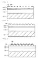
- Fig. 1
- is a side-sectional view illustrating a semiconductor light emitting device according to a first embodiment.
- Fig. 2
- is a view illustrating a protruding structure of a second conductive type semiconductor layer of
Fig. 1 . - Fig. 3
- is a view illustrating an example of light reflection at an interface between the second conductive type semiconductor layer and the second electrode layer of
Fig. 1 . - Figs. 4
- through 8 are views illustrating a process for manufacturing a semiconductor light emitting device according to a first embodiment.
- Fig. 9
- is a side cross-sectional view of a semiconductor light emitting device according to a second embodiment.
- Fig. 10
- is a graph illustrating an optical power with respect to an injection current in semiconductor light emitting devices according to a first embodiment and a comparative embodiment.
- Fig. 11
- is a side cross-sectional view illustrating a light emitting device package according to a third embodiment.
- Reference will now be made in detail to the embodiments of the present disclosure, examples of which are illustrated in the accompanying drawings. In description of embodiments, the 'on' or 'under' of each layer may be described with reference to the accompanying drawings, and the thickness of the each layer will also be described as an example and is not limited to the thickness shown in the accompanying drawings.
- In the description of embodiments, it will be understood that when a layer (or film), region, pattern or structure is referred to as being 'on' or 'under' another layer (or film), region, pad or pattern, the terminology of 'on' and 'under' includes both the meanings of 'directly' and 'indirectly'.
-
Fig. 1 is a side-sectional view illustrating a semiconductor light emitting device according to a first embodiment.Fig. 2 is a view illustrating a protruding structure of a second conductive type semiconductor layer ofFig. 1. Fig. 3 is a view illustrating an example of light reflection at an interface between the second conductive type semiconductor layer and the second electrode layer ofFig. 1 . - Referring to
Fig. 1 , a semiconductorlight emitting device 100 includes a first conductivetype semiconductor layer 110, anactive layer 120, a second conductivetype semiconductor layer 130, afirst semiconductor layer 135, asecond electrode layer 150 of an uneven shape, aconductive support member 160, and afirst electrode 170. - The semiconductor
light emitting device 100 includes an LED using a plurality of compound semiconductors, for example, compound semiconductors of group III-V elements. The LED may be a colored LED or a UV LED which emits blue light, green light, or red light. Light emitted by the LED may be diversely implemented within the technical scope of embodiments. - The plurality of compound semiconductor layers include a first conductive
type semiconductor layer 110, anactive layer 120, and a second conductivetype semiconductor layer 130. - The first conductive
type semiconductor layer 110 may be selected from the compound semiconductors of group III-V elements doped with a first conductive type dopant, for example, GaN, AlN, AlGaN, InGaN, InN, InAlGaN, AlInN, AlGaAs, GaP, GaAs, GaAsP and AlGaInP. When the first conductivetype semiconductor layer 110 is an N-type semiconductor layer, the first conductive type dopant may include an N-type dopant such as Si, Ge, Sn, Se, Te. The first conductivetype semiconductor layer 110 may be formed as a mono- or a multi-layer, but is not limited thereto. - A
first electrode 170 is formed under the first conductivetype semiconductor layer 110. Thefirst electrode 170 is formed in a certain shape or pattern, but is not limited thereto. Aroughness pattern 115 may be formed on the undersurface of the first conductivetype semiconductor layer 110. - The
active layer 120 is formed on the first conductivetype semiconductor layer 110, and may be formed in a single- or a multiple quantum well structure. Theactive layer 120 may be formed to have the periodic lamination of a well layer and a barrier layer, for example, an InGaN well layer/GaN barrier layer, an InGaN well layer/AlGaN barrier layer, or InGaN well layer/InGaN well layer using the compound semiconductor materials of group III-V elements. A conductive type clad layer may be formed on and/or under theactive layer 120, and may be formed of a GaN-based semiconductor. - The second conductive
type semiconductor layer 130 may be formed on theactive layer 120, and may be selected from the compound semiconductors of group III-V elements doped with a second conductive type dopant, for example, GaN, AlN, AlGaN, InGaN, InN, InAlGaN, AlInN, AlGaAs, GaP, GaAs, GaAsP and AlGaInP. When the second conductivetype semiconductor layer 130 is a P-type semiconductor layer, the second conductive type dopant may include a P-type dopant such as Mg and Zn. The secondconductive semiconductor layer 130 may be formed in a mono- or a multi-layer, but is not limited thereto. - The first conductive
type semiconductor layer 110, theactive layer 120, and the second conductivetype semiconductor layer 130 may be defined as a light emitting structure. - An N-type semiconductor layer or a P-type semiconductor layer may be formed on the second conductive
type semiconductor layer 130. The first conductivetype semiconductor layer 110 may be implemented in a P-type semiconductor layer, and the second conductivetype semiconductor layer 130 may be implemented in an N-type semiconductor layer. Thus, the light emitting structure may include at least one of an N-P junction, a P-N junction, an N-P-N junction, and a P-N-P junction. - The
first semiconductor layer 135 is formed on the second conductivetype semiconductor layer 130. Thefirst semiconductor layer 135 may be protruded from the upper surface of the second conductivetype semiconductor layer 130, and may be formed at a regular or irregular interval. Thefirst semiconductor layer 135 is formed to have a discontinuous protrusion, for example, a cone shape or a pyramid shape. - The
first semiconductor layer 135 may be formed of the same or different semiconductor material from the second conductivetype semiconductor layer 130. Thefirst semiconductor layer 135 may be formed of at least one of, for example, GaN, AlN, AlGaN, InGaN, InN, InAlGaN, AlInN, AlGaAs, GaP, GaAs, GaAsP, and AlGaInP. Thefirst semiconductor layer 135 may be formed of an undoped semiconductor layer, a semiconductor layer doped with a first conductive type dopant, a semiconductor doped with a second conductive type dopant. - Referring to
Fig. 2 , the thickness T of thefirst semiconductor layer 135 may ranges from about 0.1 µm to about 2 µm. The maximum diameter of thefirst semiconductor layer 135 may ranges from about 1.0 µm to about 10 µm. - One side surface of the
first semiconductor layer 135 may be inclined at an inside angle θ of, for example, about 55 degrees to about 57 degrees with the respect to the horizontal surface of the second conductivetype semiconductor layer 130. Here, the inside angle θ of thefirst semiconductor layer 135 may vary with the crystal properties of a material forming thefirst semiconductor layer 135. The interval between the protrusions of thefirst semiconductor layer 135 may range from about 100nm to about 100 µm. - The shape of the
first semiconductor layer 135 may be formed in a three-dimensional shape, for example, a cone shape or a pyramid shape with various base surfaces such as a diamond shape, having an inclined sidewall, but can be modified within the technical scope of the embodiments. Thefirst semiconductor layer 135 may be formed in a tapered shape, the width of the upper part of which is smaller than that of the lower part. - Here, the
first semiconductor layer 135 may be formed at a regular or irregular interval on the second conductivetype semiconductor layer 130 through a selective growth or etching method. - Referring to
Fig. 1 , thefirst semiconductor layer 135 is protruded from the surface of the second conductivetype semiconductor layer 130 to have an uneven structure. - A
second electrode layer 150 is formed on the second conductivetype semiconductor layer 130 and thefirst semiconductor layer 135. The undersurface of thesecond electrode layer 150 may have an uneven shape corresponding to the shape of thefirst semiconductor layer 130. - The uneven shape of the
second electrode layer 150 may have the same angle and shape as the shape of thefirst semiconductor layer 135. The protruding shape of thesecond electrode layer 150 may be inclined. Thesecond electrode layer 150 may be formed in a cone or inverse-cone shape along the second conductivetype semiconductor layer 130. - The
second electrode layer 150 may include at least one of an ohmic contact layer, a reflection layer, and an adhesive layer. The ohmic contact layer may include at least one of, for example, indium tin oxide (ITO), indium zinc oxide (IZO), indium zinc tin oxide (IZTO), indium aluminum zinc oxide (IAZO), indium gallium zinc oxide (IGZO), indium gallium tin oxide (IGTO), aluminum zinc oxide (AZO) and antimony tin oxide (ATO), gallium zinc oxide (GZO), IrOx, RuOx, RuOx/ITO, Ni/IrOx/Au, Ni/IrOx/Au/ITO, Pt, Ni, Au, Rh and Pd. The reflection layer may include a layer formed of Ag, Ni, Al, Rh, Pd, Ir, Ru, Mg, Zn, Pt, Au, Hf, or an alloy of at least two thereof. The adhesive layer may include at least one of Ti, Au, Sn, Ni, Cr, Ga, In, Bi, Cu, Ag, and Ta. - The
second electrode layer 150 may be used as a seed layer for a plating process. - The recess of the
second electrode layer 150 is formed on the second conductivetype semiconductor layer 130, and the protrusion of thesecond electrode layer 150 is formed to have a shape corresponding to thefirst semiconductor layer 135. At least one of the recess and protrusion of thesecond electrode layer 150 may be formed to be an inferior conductive region. - Also, an ohmic contact layer (not shown) may be formed between the
second electrode layer 150 and the second conductivetype semiconductor layer 130. The ohmic contact layer may be formed to have a layered shape or a multiple-pattern on the second conductivetype semiconductor layer 130, but is not limited thereto. The ohmic contact layer may include at least one of indium tin oxide (ITO), indium zinc oxide (IZO), indium zinc tin oxide (IZTO), indium aluminum zinc oxide (IAZO), indium gallium zinc oxide (IGZO), indium gallium tin oxide (IGTO), aluminum zinc oxide (AZO) and antimony tin oxide (ATO), gallium zinc oxide (GZO), IrOx, RuOx, RuOx/ITO, Ni/IrOx/Au, Ni/IrOx/Au/ITO, Ni/IrOx/Au, and Ni/IrOx/Au/ITO, but embodiments are not limited thereto. A nonconductor layer, for example, an MgN layer may be formed between thesecond electrode layer 150 and the second conductivetype semiconductor layer 130. The nonconductor layer may be disposed between the discontinuous first semiconductor layers 135. - The
first semiconductor layer 135 may be formed of a semiconductor of the same or different polarity from the second conductivetype semiconductor layer 130. Thefirst semiconductor layer 130 may be formed of an undoped semiconductor, a semiconductor doped with a first conductive type dopant, or a semiconductor doped with a second conductive type dopant. - When the
first semiconductor layer 135 is formed of an undoped semiconductor or a first conductive type semiconductor, a current applied to thesecond electrode layer 150 may be supplied to the second conductivetype semiconductor layer 130 disposed between the first semiconductor layers 135. - When a nonconductor layer is disposed between the first semiconductor layers 135, the current applied to the second electrode layer may be supplied to the second conductive
type semiconductor layer 130 through thefirst semiconductor layer 135. - When the
first semiconductor layer 135 is a second conductive type semiconductor, the current applied to thesecond electrode layer 150 may be supplied to thefirst semiconductor layer 135 and the second conductivetype semiconductor layer 130. - A
conductive support member 160 may be formed on thesecond electrode layer 150, and may serve as a base substrate. Theconductive support member 160 may be implemented using Cu, Au, Ni, Mo, Cu-W, and carrier wafer such as Si, Ge, GaAs, ZnO, SiC, SiGe, and GaN. Theconductive support member 160 may be formed by an electroplating method, or may be formed in a sheep shape, but is not limited thereto. - The lower part of the
conductive support member 160 may be formed to have a structure corresponding to the unevenness of thesecond electrode layer 150. The thickness of theconductive support member 160 may range from about 30 µm to about 150 µm, but embodiments are not limited thereto. Thesecond electrode layer 150 and theconductive support member 160 may be formed as a reflection electrode layer, for example, a second electrode unit, but is not limited thereto. - The semiconductor
light emitting device 100 is supplied with power through thefirst electrode 170 and theconductive support member 160, light is emitted from theactive layer 120 in all directions. - A portion of the light emitted from the
active layer 120 travels to thesecond electrode layer 150. Thesecond electrode layer 150 may change the critical angle of the incident light using the unevenness structure, thereby improving the external quantum efficiency. - Referring to
Figs. 1 and 3 , the light emitting to thesecond electrode layer 150 is reflected by the change of the critical angle. Thesecond electrode layer 150 changes the reflection angle of the incident light. In this case, thesecond electrode layer 150 may change the reflection angle of light smaller than the critical angle that allows the emission of light, thereby increasing a possibility that light is extracted to the outside. - Embodiments can improve the external quantum efficiency using a discontinuous
first semiconductor layer 135 and asecond electrode layer 150 having an uneven shape on a plurality of compound semiconductor layers or a light emitting structure. -
Figs. 4 through 8 are views illustrating a process for manufacturing a semiconductor light emitting device according to a first embodiment. - Referring to
Fig. 4 , asubstrate 101 is loaded into a growth system, and a compound semiconductor layer of group III to V elements may be grown thereon. - The examples of the growth systems may include electron beam evaporator, Physical Vapor Deposition (PVD), Chemical Vapor Deposition (CVD), Plasma Laser Deposition (PLD), dual-type thermal evaporator, sputtering and Metal Organic Chemical Vapor Deposition (MOCVD), but embodiments are not limited to these systems.
- The
substrate 101 may be selected from the group consisting of sapphire substrate (Al2O3), GaN, SiC, ZnO, Si, GaP, InP, Ga2O3, a conductive substrate, and GaAs. An unevenness pattern may be formed over the surface of thesubstrate 101. At least one layer or pattern, for example, a ZnO layer (not shown), a buffer layer (not shown), or an undoped semiconductor layer (not shown), which is formed of compound semiconductors of group III to V elements, may be formed over thesubstrate 101. - The buffer layer and the undoped semiconductor layer may be formed using compound semiconductors of group III-V elements. The buffer layer may reduce a difference in lattice constant from the
substrate 101. The undoped semiconductor layer may be formed of an undoped GaN-based semiconductor. - A light emitting structure including a plurality of compound semiconductor layers is formed on the
substrate 101. The light emitting structure includes a first conductivetype semiconductor layer 110, anactive layer 120 on the firstconductive semiconductor layer 110, and a second conductivetype semiconductor layer 130 on theactive layer 120. - The first conductive
type semiconductor layer 110 may be selected from the compound semiconductors of group III-V elements doped with a first conductive type dopant, for example, GaN, AlN, AlGaN, InGaN, InN, InAlGaN, AlInN, AlGaAs, GaP, GaAs, GaAsP and AlGaInP. When the firstconductive type semiconductor 110 is an N-type semiconductor layer, the first conductive type dopant includes an N-type dopant such as Si, Ge, Sn, Se and Te. The first conductivetype semiconductor layer 110 may be formed as a mono- or multi-layer, but is not limited thereto. - The
active layer 120 is formed on the first conductivetype semiconductor layer 110, and may be formed in a single- or a multiple quantum well structure. Theactive layer 120 may be formed to have the periodic lamination of a well layer and a barrier layer, for example, an InGaN well layer/GaN barrier layer, an InGaN well layer/AlGaN barrier layer, or InGaN well layer/InGaN barrier layer using the compound semiconductor materials of group III-V elements. - A conductive type clad layer may be formed on and/or under the
active layer 120, and may be formed of a GaN-based semiconductor. - The second
conductive semiconductor layer 130 is formed on theactive layer 120, and may be selected from the compound semiconductors of group III-V elements doped with a second conductive type dopant, for example, GaN, AlN, AlGaN, InGaN, InN, InAlGaN, AlInN, AlGaAs, GaP, GaAs, GaAsP and AlGaInP. When the second conductivetype semiconductor layer 130 is a P-type semiconductor layer, the second conductive type dopant may include a P-type dopant such as Mg and Zn. The second conductivetype semiconductor layer 130 may be formed as a mono- or multi-layer, but is not limited thereto. - The second conductive
type semiconductor layer 130 may include a P-type GaN layer that is formed to have a certain thickness by supplying a gas including P-type dopant such as NH3, TMGa (or TEGa), and Mg(CP2Mg). - The first conductive
type semiconductor layer 110, theactive layer 120, and the second conductivetype semiconductor layer 130 may be defined as a light emitting structure. A third conductive type semiconductor layer, for example, an N-type semiconductor layer or a P-type semiconductor layer may be formed on the second conductivetype semiconductor layer 130. Thus, the light emitting structure may include at least one of an N-P junction, a P-N junction, an N-P-N junction, and a P-N-P junction. - Referring to
Figs. 4 and 5 , the second conductivetype semiconductor layer 130 is grown with a certain thickness. Amask pattern 132 is formed on the second conductivetype semiconductor layer 130. A plurality of openingregions 134 may be formed at a regular or irregular interval on themask pattern 132. Theopening region 134 of themask pattern 132 may have a diameter ranging from about 1.0 µm to about 10 µm. The interval between the openingregions 134 of themask pattern 132 may range from about 100nm to about 100 µm. - The second conductive
type semiconductor layer 130 is regrown. For example, a P-type GaN layer may be formed to have a certain thickness by supplying a gas including P-type dopant such as NH3, TMGa (or TEGa), and Mg(CP2Mg). In this case, the growth temperature and pressure may be adjusted to form the P-type layer. Thus, afirst semiconductor layer 135 is formed using theopening region 134 of themask pattern 132. Thefirst semiconductor layer 135 may be formed to have a three-dimensional shape, which has a vertical section of a triangular shape or a polygonal shape (e.g., trapezoid) and a base plane of a circular or polygonal (e.g., hexagonal) shape. Also, the inclination of thefirst semiconductor layer 135 may have an inside angle θ ranging from about 55 degrees to about 57 degrees with respect to the upper surface of the second conductivetype semiconductor layer 130 as shown inFig. 2 . - If the
first semiconductor layer 135 is formed on the second conductivetype semiconductor layer 130, themask pattern 132 may be removed. - Here, methods for forming the
first semiconductor layer 135 will be described as follows. There are two exemplary methods for forming thefirst semiconductor layer 135. In a first method, after the second conductivetype semiconductor layer 130 may be grown to a certain thickness, a dry and/or wet etching may be performed using a mask pattern to form thefirst semiconductor layer 135 as described above. Here, thefirst semiconductor layer 135 may be formed of the same material as the second conductivetype semiconductor layer 130, but is not limited thereto. - In a second method, a nonconductor layer having an opening region may be formed on the second conductive
type semiconductor layer 130. The nonconductor layer may be implemented using an MgN layer, but is not limited thereto. Thefirst semiconductor layer 135 may be formed using the opening region of the nonconductor layer. Here, the MgN layer may be formed using Mg and ammonia (NH3). The MgN layer may be formed to have an irregular pattern. Thus, thefirst semiconductor layer 135 may be formed at an irregular interval on the second conductivetype semiconductor layer 130. Thereafter, the MgN layer may or may not be removed. Since the MgN layer is a nonconductor, a current applied to the second electrode layer may be supplied to the second conductivetype semiconductor layer 130 through thefirst semiconductor layer 135. - Consequently, the
first semiconductor layer 135 may be formed to have an uneven shape on the second conductivetype semiconductor layer 130. - The
first semiconductor layer 135 may be formed of the same or different semiconductor material from the second conductivetype semiconductor layer 130. Thefirst semiconductor layer 135 may be formed of at least one of, for example, GaN, AlN, AlGaN, InGaN, InN, InAlGaN, AlInN, AlGaAs, GaP, GaAs, GaAsP, and AlGaInP. Thefirst semiconductor layer 135 may be formed of a semiconductor of the same or different polarity from the second conductivetype semiconductor layer 130. Thefirst semiconductor layer 135 may be formed of an undoped semiconductor layer, a semiconductor layer doped with a first conductive type dopant, a semiconductor doped with a second conductive type dopant. - Referring to
Fig. 6 , asecond electrode layer 150 is formed on the second conductivetype semiconductor layer 130. Thesecond electrode layer 150 may be formed in an inside region or on the entire surface of the second conductivetype semiconductor layer 130, but is not limited thereto. - The
second electrode layer 150 may include at least one of an ohmic contact layer, a reflection layer, and an adhesive layer. The ohmic contact layer may include at least one of, for example, indium tin oxide (ITO), indium zinc oxide (IZO), indium zinc tin oxide (IZTO), indium aluminum zinc oxide (IAZO), indium gallium zinc oxide (IGZO), indium gallium tin oxide (IGTO), aluminum zinc oxide (AZO) and antimony tin oxide (ATO), gallium zinc oxide (GZO), IrOx, RuOx, RuOx/ITO, Ni/IrOx/Au, Ni/IrOx/Au/ITO, Pt, Ni, Au, Rh and Pd. The reflection layer may include a layer formed of Ag, Ni, Al, Rh, Pd, Ir, Ru, Mg, Zn, Pt, Au, Hf, or an alloy of at least two thereof. The adhesive layer may include at least one of Ti, Au, Sn, Ni, Cr, Ga, In, Bi, Cu, Ag, and Ta. - The
second electrode layer 150 may include a seed layer. The seed layer may include at least one of Ti, Cr, Ta, Cr/Au, Cr/Cu, Ti/Au, Ta/Cu, and Ta/Ti/Cu. - The
second electrode layer 150 may formed to have an uneven shape along the shape of thefirst semiconductor layer 135 of the second conductivetype semiconductor layer 130. The recess of thesecond electrode layer 150 may have an inverse cone shape, and the protrusion thereof may have a cone shape. - Here, the recess of the
second electrode layer 150 may contact the second conductivetype semiconductor layer 130, and the protrusion thereof may contact thefirst semiconductor layer 135. - When the
first semiconductor layer 135 is an undoped semiconductor or a first conductive type semiconductor, a current applied to thesecond electrode layer 150 may be supplied to the second conductivetype semiconductor layer 130 disposed between the first semiconductor layers 135. - When a nonconductor layer is disposed between the first semiconductor layers 135, the current applied to the second electrode layer may be supplied to the second conductive
type semiconductor layer 130 through thefirst semiconductor layer 135. - When the
first semiconductor layer 135 is a second conductive type semiconductor, the current applied to thesecond electrode layer 150 may be supplied through thefirst semiconductor layer 135 and the second conductivetype semiconductor layer 130. - Also, an ohmic contact layer (not shown) may be formed between the
second electrode layer 150 and the second conductivetype semiconductor layer 130. The ohmic contact layer may be formed with a layered shape or multiple-pattern before thesecond electrode layer 150 is formed. The ohmic contact layer may include at least one of indium tin oxide (ITO), indium zinc oxide (IZO), indium zinc tin oxide (IZTO), indium aluminum zinc oxide (IAZO), indium gallium zinc oxide (IGZO), indium gallium tin oxide (IGTO), aluminum zinc oxide (AZO) and antimony tin oxide (ATO), gallium zinc oxide (GZO), IrOx, RuOx, RuOx/ITO, Ni/IrOx/Au, Ni/IrOx/Au/ITO, Ni/IrOx/Au, and Ni/IrOx/Au/ITO. - Referring to
Fig. 7 , aconductive support member 160 may be formed on thesecond electrode layer 150, and may serve as a base substrate. Theconductive support member 160 may be implemented using Cu, Au, Ni, Mo, Cu-W, and carrier wafer such as Si, Ge, GaAs, ZnO, SiC, SiGe, and GaN. - The
conductive support member 160 may be formed by an electroplating method, or may be formed in a sheep shape, but is not limited thereto. The thickness of theconductive support member 160 may range from about 30 µm to about 150 µm, but embodiments are not limited thereto. - The lower part of the
conductive support member 160 may be formed to have an evenness matching the unevenness of thesecond electrode layer 150. - Referring to
Figs. 7 and 8 , theconductive support member 160 may be positioned at the base after theconductive support member 160 is formed. Then, thesubstrate 101 may be removed through a physical and/or chemical removal method. - Through the physical removal method, the
substrate 101 may be separated by a Laser Lift Off (LLO) of irradiating a laser having a wavelength of a certain range on the substrate. In the chemical removal method, when another semiconductor layer (e.g., buffer layer) is interposed between thesubstrate 101 and the first conductivetype semiconductor layer 110, thesubstrate 101 may be separated by using a wet etchant to remove the buffer layer. - An etching process such as Inductively Coupled Plasma/Reactive Ion Etching (ICP/RIE) or a grinding process may be performed on the surface of the first conductive
type semiconductor layer 110 after thesubstrate 101 is removed. - The unevenness of the
first semiconductor layer 135 of the second conductivetype semiconductor layer 130 and thesecond electrode layer 140 may reinforce an adhesive strength between the compound semiconductor layer (e.g., 130) and thesecond electrode layer 140. Accordingly, even when a laser of the LLO method is irradiated, a peeling between thecompound semiconductor layer 130 and thesecond electrode layer 140 can be overcome. - A
roughness pattern 115 may be formed on the undersurface of the first conductivetype semiconductor layer 110 through a wet and/or dry etching method. - Then, after a mesa etching is performed on a boundary region between chips (i.e., channel region), the semiconductor
light emitting device 100 may be separated into unit chips. Afirst electrode 170 having a certain pattern may be formed under the first conductivetype semiconductor layer 110. Here, a process for forming thefirst electrode 170 may be performed before or after the mesa etching, or after the separation of the semiconductorlight emitting device 100, but is not limited thereto. The first conductivetype semiconductor layer 110, theactive layer 120, and the second conductivetype semiconductor layer 130 may be formed to haveouter edges 103 thereof partially cut away. However, the mesa etching is merely a process for separation between chips, and embodiments are not limited thereto. - If a forward current is applied to the semiconductor
light emitting device 100 through thefirst electrode 170 and theconductive support member 160, light is emitted from theactive layer 120 in all directions. In this case, the light incident to thefirst semiconductor layer 135 and thesecond electrode layer 150 of the second conductivetype semiconductor layer 130 may be reflected by a change of the critical angle. That is, the reflection angle of the light incident to thesecond electrode layer 150 of the unevenness structure may be changed to be reflected. Thesecond electrode layer 150 can reflect light having a reflection angle smaller than the critical angle that allows the emission of light. In this case, the light can be reflected at a greater angle than the critical angle, thereby improving the light extraction efficiency. -
Fig. 9 is a side cross-sectional view of a semiconductor light emitting device according to a second embodiment. In the description of the second embodiment, detailed descriptions of identical parts to those of the first embodiment will be substituted with those of the first embodiment and be omitted herein. - Referring to
Fig. 8 , a semiconductorlight emitting device 100A includes a light-transmittingchannel layer 140 surrounding the circumference of the upper surface of the second conductivetype semiconductor layer 130. - The
channel layer 140 may be formed to have a ring, strip, or flame shape of a continuous or discontinuous pattern along the circumference of the second conductivetype semiconductor layer 130. That is, thechannel layer 140 may be formed with an open loop shape or closed loop shape. At least a portion of thechannel layer 140 may be exposed to a channel region of a light emitting structure, and may be formed to protect the outer wall of the light emitting structure from humidity or short-circuit. - The
channel layer 140 may be formed to have a certain width along the circumference of the second conductivetype semiconductor layer 130. The inner side of thechannel layer 140 is disposed between thesecond electrode layer 150 and the second conductivetype semiconductor layer 130, and the outer side of thechannel layer 140 is disposed under thesecond electrode layer 150. In this case, the outer side of thechannel layer 140 is exposed to thechannel region 103 of thecompound semiconductor layer - The
channel layer 140 may be formed of a light-transmitting insulating material or light-transmitting conductive material, and may include at least one of, for example, SiO2, SiOx, SiOxNy, Si3N4, Al2O3, TiO2, ITO (indium tin oxide), IZO(indium zinc oxide), IZTO(indium zinc tin oxide), IAZO(indium aluminum zinc oxide), IGZO(indium gallium zinc oxide), IGTO(indium gallium tin oxide), AZO(aluminum zinc oxide), ATO(antimony tin oxide), GZO(gallium zinc oxide), IrOx, RuOx, RuOx/ITO, Ni/IrOx/Au, and Ni/IrOx/Au/ITO. Besides the above materials, thechannel layer 140 may use a light-transmitting material or a material that is rarely fragmented by a laser light, but embodiments are not limited thereto. - The
channel layer 140 may allow theconductive support member 160 to be spaced from the second conductivetype semiconductor layer 130. Thechannel layer 140 may minimize metal material fragments generated by a laser beam during a manufacturing process of a semiconductor. -
Fig. 10 is a graph illustrating an optical power with respect to an injection current in semiconductor light emitting devices according to an embodiment and a comparative embodiment. - Referring to
Fig. 10 , when an injection current of a semiconductor light emitting device is increased, an output power of an embodiment E2 is increased by a certain gap G compared to a comparative embodiment E1. Here, the comparative embodiment E1 represents a case where a first semiconductor layer and a second electrode layer on a second conductive type semiconductor layer are flat. -
Fig. 11 is a side cross-sectional view illustrating a light emitting device package according to a third embodiment. - Referring to
Fig. 11 , the light emitting package includes abody part 20, first and secondlead electrode 31 and 32 in thebody part 20, alight emitting device 100 to which the first and secondlead electrodes 31 and 32 are electrically connected, and amolding member 40 surrounding thelight emitting device 100. - The
body part 20 may be formed of silicon, compound resin, or metal, and may have an inclined surface around thelight emitting device 100. - The first and second
lead electrodes 31 and 32 are electrically isolated from each other, and provide power to thelight emitting device 100. Also, the first and secondlead electrodes 31 and 32 may reflect light generated in thelight emitting device 100, thereby increasing optical efficiency. The first and secondlead electrodes 31 and 32 also serve to exhaust heat generated in thelight emitting device 100 to the outside. - The
light emitting device 100 may be disposed on thebody part 20 or the first and secondlead electrodes 31 and 32. - The
light emitting device 100 may be electrically connected to the first lead electrode 31 through a wire, and may be electrically connected to thelead electrode 32 through a die bonding. - The
molding member 40 surrounds thelight emitting device 100 to protect thelight emitting device 100. Also, the moldingmember 40 may include a phosphor to change the wavelength of light emitted from thelight emitting device 100. - After the semiconductor light emitting device according to the embodiment(s) is die-bonded to the
second lead electrode 32 through an insulating substrate or a growth substrate, which is packaged to be used as a light source of indicating devices, lighting device, and displaying devices. - In still further another embodiment, a method for manufacturing a semiconductor light emitting device comprises: forming a plurality of compound semiconductor layers comprising a first conductive type semiconductor layer, an active layer, and a second conductive type semiconductor layer; forming a first semiconductor layer discontinuously protruding from the second conductive type semiconductor layer; forming a second electrode layer a second electrode layer on the second conductive type semiconductor layer and the first semiconductor layer; forming a conductive support member on the second electrode layer; and forming a first electrode under the first conductive type semiconductor layer.
- Features, structures, and effects described in the above embodiments are incorporated into at least one embodiment of the present invention, but are not limited to only one embodiment. Moreover, features, structures, and effects exemplified in one embodiment can easily be combined and modified for another embodiment by those skilled in the art. Therefore, these combinations and modifications should be construed as falling within the scope of the present invention.
- A semiconductor light emitting device or a light emitting device package according to an embodiment can be used as light sources of displaying device, indicating devices, and lighting devices, but is not limited thereto.
- Embodiments can provide a semiconductor light emitting device such as an LED.
- Embodiments can improve electrical reliability of a semiconductor light emitting device.
- Embodiments can improve optical efficiency of a vertical-type semiconductor light emitting device.
- Embodiments can apply light source packaged with a semiconductor light emitting device to lighting devices, indicating devices, and displaying devices.
- Embodiments can improve external quantum efficiency.
- Embodiments can enhance an adhesive strength between a semiconductor layer and a second electrode layer.
- Embodiments can improve reliability of a semiconductor light emitting device.
- Although embodiments have been described with reference to a number of illustrative embodiments thereof, it should be understood that numerous other modifications and embodiments can be devised by those skilled in the art that will fall within the spirit and scope of the principles of this disclosure. More particularly, various variations and modifications are possible in the component parts and/or arrangements of the subject combination arrangement within the scope of the disclosure, the drawings and the appended claims. In addition to variations and modifications in the component parts and/or arrangements, alternative uses will also be apparent to those skilled in the art.
Claims (15)
- A semiconductor light emitting device, comprising:a plurality of compound semiconductor layers comprising a first conductive type semiconductor layer, an active layer, and a second conductive type semiconductor layer;a first electrode under the plurality of compound semiconductor layers;a second electrode layer having an unevenness on the plurality of compound semiconductor layers; anda conductive support member on the second electrode layer.
- The semiconductor light emitting device according to claim 1, wherein the unevenness of the second electrode layer has a three-dimensional shape.
- The semiconductor light emitting device according to claim 1, comprising a first semiconductor layer discontinuously formed between the second conductive type semiconductor layer and the second electrode layer.
- The semiconductor light emitting device according to claim 3, wherein the first semiconductor layer is disposed at a regular or irregular interval.
- The semiconductor light emitting device according to claim 3, wherein the first semiconductor layer comprises the same or different semiconductor material from the second conductive type semiconductor layer.
- The semiconductor light emitting device according to claim 3, wherein the first semiconductor layer comprises at least one of compound semiconductors of group III-V elements.
- The semiconductor light emitting device according to claim 3, wherein the first semiconductor layer comprises at least one of a first conductive type semiconductor, an undoped semiconductor, and a second conductive type semiconductor.
- The semiconductor light emitting device according to claim 3, wherein at least one of a recess and a protrusion of the second electrode layer includes an inferior conductive region.
- The semiconductor light emitting device according to claim 1, wherein the unevenness of the second electrode layer has a protrusion inclined to the second conductive type semiconductor layer.
- The semiconductor light emitting device according to claim 9, wherein the protrusion of the unevenness of the second electrode layer has an inclined surface of about 55 degrees to about 57 degrees with respect to the second conductive type semiconductor layer.
- A semiconductor light emitting device, comprising:a plurality of compound semiconductor layers comprising a first conductive type semiconductor layer, an active layer, and a second conductive type semiconductor layer;a first electrode under the plurality of compound semiconductor layers;a light-transmitting channel layer around a circumference of an upper surface of the plurality of compound semiconductor layers;a second electrode layer having an unevenness on the compound semiconductor layer; anda conductive support member on the second electrode layer.
- The semiconductor light emitting device according to claim 11, comprising a first semiconductor layer discontinuously formed between the second conductive type semiconductor layer and the second electrode layer.
- The semiconductor light emitting device according to claim 11, wherein the first semiconductor layer has the same or different polarity from the second conductive type semiconductor layer.
- The semiconductor light emitting device according to claim 11, wherein the light-transmitting channel layer comprises at least one of SiO2, SiOx, SiOxNy, Si3N4, Al2O3, TiO2, indium tin oxide (ITO), indium zinc oxide (IZO), indium zinc tin oxide (IZTO), indium aluminum zinc oxide (IAZO), indium gallium zinc oxide (IGZO), indium gallium tin oxide (IGTO), aluminum zinc oxide (AZO) and antimony tin oxide (ATO), gallium zinc oxide (GZO), IrOx, RuOx, RuOx/ITO, Ni/IrOx/Au, Ni/Irox/Au/ITO.
- A semiconductor light emitting device, comprising:a plurality of compound semiconductor layers comprising a first conductive type semiconductor layer, an active layer, and a second conductive type semiconductor layer;a first semiconductor layer discontinuously protruding from the second conductive type semiconductor layer;a first electrode under the first conductive type semiconductor layer;a light-transmitting channel layer around a circumference of an upper surface of the second conductive type semiconductor layer;a second electrode layer on the second conductive type semiconductor layer and the first semiconductor layer; anda conductive support member on the second electrode layer.
Applications Claiming Priority (1)
| Application Number | Priority Date | Filing Date | Title |
|---|---|---|---|
| KR1020080114280A KR101103882B1 (en) | 2008-11-17 | 2008-11-17 | Semiconductor light emitting device and fabrication method thereof |
Publications (3)
| Publication Number | Publication Date |
|---|---|
| EP2187456A2 true EP2187456A2 (en) | 2010-05-19 |
| EP2187456A3 EP2187456A3 (en) | 2014-02-26 |
| EP2187456B1 EP2187456B1 (en) | 2018-09-26 |
Family
ID=41718506
Family Applications (1)
| Application Number | Title | Priority Date | Filing Date |
|---|---|---|---|
| EP09014265.4A Active EP2187456B1 (en) | 2008-11-17 | 2009-11-16 | Semiconductor light emitting device |
Country Status (4)
| Country | Link |
|---|---|
| US (2) | US8222656B2 (en) |
| EP (1) | EP2187456B1 (en) |
| KR (1) | KR101103882B1 (en) |
| CN (1) | CN101740698B (en) |
Cited By (6)
| Publication number | Priority date | Publication date | Assignee | Title |
|---|---|---|---|---|
| EP2645432A1 (en) * | 2010-09-30 | 2013-10-02 | Enraytek Optoelectronics Co., Ltd. | Light emitting device and manufacturing method thereof |
| EP2405497A3 (en) * | 2010-07-05 | 2015-03-11 | LG Innotek Co., Ltd. | Light emitting device having an roughened surface and method of manufacturing the same |
| EP2624318A4 (en) * | 2010-09-30 | 2015-11-11 | Dowa Electronics Materials Co | Iii nitride semiconductor light-emitting element, and process for manufacturing same |
| EP2560216B1 (en) * | 2010-11-09 | 2016-11-30 | Enraytek Optoelectronics Co., Ltd. | Light emitting diode and manufacturing method thereof, light emitting device |
| WO2019158425A1 (en) * | 2018-02-14 | 2019-08-22 | Osram Opto Semiconductors Gmbh | Optoelectronic semiconductor component and method for producing an optoelectronic semiconductor component |
| EP4047761A1 (en) * | 2021-02-22 | 2022-08-24 | Kabushiki Kaisha Toshiba | Surface light-emission type semiconductor light-emitting device |
Families Citing this family (17)
| Publication number | Priority date | Publication date | Assignee | Title |
|---|---|---|---|---|
| US8242690B2 (en) * | 2005-04-29 | 2012-08-14 | Evergrand Holdings Limited | Light-emitting diode die packages and illumination apparatuses using same |
| KR101658838B1 (en) * | 2010-02-04 | 2016-10-04 | 엘지이노텍 주식회사 | Light emitting device and method for fabricating the same |
| KR100986397B1 (en) * | 2010-02-08 | 2010-10-08 | 엘지이노텍 주식회사 | Light emitting apparatus |
| KR100999736B1 (en) * | 2010-02-17 | 2010-12-08 | 엘지이노텍 주식회사 | Light emitting device, method for fabricating the light emitting device and lighting unit |
| JP5733594B2 (en) * | 2010-02-18 | 2015-06-10 | スタンレー電気株式会社 | Semiconductor light emitting device |
| EP2442374B1 (en) | 2010-10-12 | 2016-09-21 | LG Innotek Co., Ltd. | Light emitting device |
| US20130130417A1 (en) * | 2011-11-22 | 2013-05-23 | Jar-Yu WU | Manufacturing method of a light-emitting device |
| KR101973608B1 (en) * | 2011-06-30 | 2019-04-29 | 엘지이노텍 주식회사 | Light emitting device |
| KR101880445B1 (en) * | 2011-07-14 | 2018-07-24 | 엘지이노텍 주식회사 | Light emitting device, method of fabricating light emitting device, light emitting device package, and light unit |
| KR101871503B1 (en) * | 2011-09-06 | 2018-06-27 | 엘지이노텍 주식회사 | Light emitting device and method for fabricating the same |
| US8952413B2 (en) * | 2012-03-08 | 2015-02-10 | Micron Technology, Inc. | Etched trenches in bond materials for die singulation, and associated systems and methods |
| KR20220145922A (en) * | 2012-12-25 | 2022-10-31 | 가부시키가이샤 한도오따이 에네루기 켄큐쇼 | Semiconductor device |
| JP6248786B2 (en) * | 2014-04-25 | 2017-12-20 | 日亜化学工業株式会社 | Nitride semiconductor device and manufacturing method thereof |
| KR102203690B1 (en) * | 2014-08-21 | 2021-01-15 | 엘지이노텍 주식회사 | Phosphor plate and manufacturing method thereof |
| FR3038451B1 (en) * | 2015-06-30 | 2017-07-21 | Commissariat Energie Atomique | ELECTROLUMINESCENT DEVICE. |
| WO2021151828A1 (en) | 2020-01-30 | 2021-08-05 | Basf Se | The use of a polylysine for increasing the gloss of hair |
| WO2021239622A1 (en) | 2020-05-27 | 2021-12-02 | Basf Se | Branched amino-acid-based polymers for hair strengthening |
Citations (5)
| Publication number | Priority date | Publication date | Assignee | Title |
|---|---|---|---|---|
| US4514896A (en) * | 1981-03-25 | 1985-05-07 | At&T Bell Laboratories | Method of forming current confinement channels in semiconductor devices |
| US20040178415A1 (en) * | 2002-03-12 | 2004-09-16 | Jung-Kuei Hsu | Light-emitting diode with enhanced brightness and method for fabricating the same |
| US20050067625A1 (en) * | 2003-09-29 | 2005-03-31 | Sanyo Electric Co., Ltd. | Semiconductor light-emitting device |
| US20050258444A1 (en) * | 2004-04-30 | 2005-11-24 | Osram Opto Semiconductors Gmbh | Semiconductor chip for optoelectronics and method for the production thereof |
| US20050282373A1 (en) * | 2000-04-26 | 2005-12-22 | Osram Gmbh, A Germany Corporation | Radiation-emitting semiconductor element and method for producing the same |
Family Cites Families (18)
| Publication number | Priority date | Publication date | Assignee | Title |
|---|---|---|---|---|
| TW564584B (en) * | 2001-06-25 | 2003-12-01 | Toshiba Corp | Semiconductor light emitting device |
| JP4223797B2 (en) * | 2002-12-19 | 2009-02-12 | 株式会社東芝 | Nitride-based semiconductor light-emitting device and manufacturing method thereof |
| US7102175B2 (en) * | 2003-04-15 | 2006-09-05 | Matsushita Electric Industrial Co., Ltd. | Semiconductor light-emitting device and method for fabricating the same |
| EP1667241B1 (en) * | 2003-08-19 | 2016-12-07 | Nichia Corporation | Semiconductor light emitting diode and method of manufacturing the same |
| US7119372B2 (en) * | 2003-10-24 | 2006-10-10 | Gelcore, Llc | Flip-chip light emitting diode |
| JP2005191220A (en) | 2003-12-25 | 2005-07-14 | Sanken Electric Co Ltd | Semiconductor light emitting element and its manufacturing method |
| JP4868709B2 (en) * | 2004-03-09 | 2012-02-01 | 三洋電機株式会社 | Light emitting element |
| EP2426743B1 (en) * | 2004-10-22 | 2019-02-20 | Seoul Viosys Co., Ltd | GaN compound semiconductor light emitting element and method of manufacturing the same |
| CN100477425C (en) * | 2005-05-19 | 2009-04-08 | 松下电器产业株式会社 | Nitride semiconductor device and method for manufacturing same |
| JP4830356B2 (en) * | 2005-06-08 | 2011-12-07 | ソニー株式会社 | Semiconductor light emitting device and semiconductor light emitting device |
| KR101008285B1 (en) * | 2005-10-28 | 2011-01-13 | 주식회사 에피밸리 | ?-nitride semiconductor light emitting device |
| KR100640497B1 (en) | 2005-11-24 | 2006-11-01 | 삼성전기주식회사 | Vertically structured gan type led device |
| KR100896576B1 (en) | 2006-02-24 | 2009-05-07 | 삼성전기주식회사 | Nitride-based semiconductor light emitting device and method of manufacturing the same |
| JP5232969B2 (en) | 2006-03-23 | 2013-07-10 | 豊田合成株式会社 | Method for manufacturing gallium nitride compound semiconductor light emitting device |
| JP2008091862A (en) * | 2006-09-08 | 2008-04-17 | Sharp Corp | Nitride semiconductor light emitting device, and manufacturing method of nitride semiconductor light emitting device |
| KR100815225B1 (en) * | 2006-10-23 | 2008-03-19 | 삼성전기주식회사 | Vertically structured light emitting diode device and method of manufacturing the same |
| EP2176891B1 (en) * | 2007-07-19 | 2018-12-26 | Lumileds Holding B.V. | Vertical led with conductive vias |
| KR100992776B1 (en) * | 2008-11-14 | 2010-11-05 | 엘지이노텍 주식회사 | Semiconductor light emitting device and fabrication method thereof |
-
2008
- 2008-11-17 KR KR1020080114280A patent/KR101103882B1/en active IP Right Grant
-
2009
- 2009-11-16 US US12/619,038 patent/US8222656B2/en not_active Expired - Fee Related
- 2009-11-16 EP EP09014265.4A patent/EP2187456B1/en active Active
- 2009-11-17 CN CN2009102247614A patent/CN101740698B/en not_active Expired - Fee Related
-
2012
- 2012-07-16 US US13/550,482 patent/US8421101B2/en active Active
Patent Citations (5)
| Publication number | Priority date | Publication date | Assignee | Title |
|---|---|---|---|---|
| US4514896A (en) * | 1981-03-25 | 1985-05-07 | At&T Bell Laboratories | Method of forming current confinement channels in semiconductor devices |
| US20050282373A1 (en) * | 2000-04-26 | 2005-12-22 | Osram Gmbh, A Germany Corporation | Radiation-emitting semiconductor element and method for producing the same |
| US20040178415A1 (en) * | 2002-03-12 | 2004-09-16 | Jung-Kuei Hsu | Light-emitting diode with enhanced brightness and method for fabricating the same |
| US20050067625A1 (en) * | 2003-09-29 | 2005-03-31 | Sanyo Electric Co., Ltd. | Semiconductor light-emitting device |
| US20050258444A1 (en) * | 2004-04-30 | 2005-11-24 | Osram Opto Semiconductors Gmbh | Semiconductor chip for optoelectronics and method for the production thereof |
Cited By (10)
| Publication number | Priority date | Publication date | Assignee | Title |
|---|---|---|---|---|
| EP2405497A3 (en) * | 2010-07-05 | 2015-03-11 | LG Innotek Co., Ltd. | Light emitting device having an roughened surface and method of manufacturing the same |
| EP2645432A1 (en) * | 2010-09-30 | 2013-10-02 | Enraytek Optoelectronics Co., Ltd. | Light emitting device and manufacturing method thereof |
| EP2645432A4 (en) * | 2010-09-30 | 2014-07-30 | Enraytek Optoelectronics Co | Light emitting device and manufacturing method thereof |
| EP2897181A1 (en) * | 2010-09-30 | 2015-07-22 | Enraytek Optoelectronics Co., Ltd. | Method for manufacturing a light emitting device |
| EP2624318A4 (en) * | 2010-09-30 | 2015-11-11 | Dowa Electronics Materials Co | Iii nitride semiconductor light-emitting element, and process for manufacturing same |
| US9263642B2 (en) | 2010-09-30 | 2016-02-16 | Dowa Electronics Materials Co., Ltd. | III nitride semiconductor light emitting device and method for manufacturing the same |
| EP2560216B1 (en) * | 2010-11-09 | 2016-11-30 | Enraytek Optoelectronics Co., Ltd. | Light emitting diode and manufacturing method thereof, light emitting device |
| WO2019158425A1 (en) * | 2018-02-14 | 2019-08-22 | Osram Opto Semiconductors Gmbh | Optoelectronic semiconductor component and method for producing an optoelectronic semiconductor component |
| US11949052B2 (en) | 2018-02-14 | 2024-04-02 | Osram Oled Gmbh | Optoelectronic semiconductor component and method of producing an optoelectronic semiconductor component |
| EP4047761A1 (en) * | 2021-02-22 | 2022-08-24 | Kabushiki Kaisha Toshiba | Surface light-emission type semiconductor light-emitting device |
Also Published As
| Publication number | Publication date |
|---|---|
| KR101103882B1 (en) | 2012-01-12 |
| US8421101B2 (en) | 2013-04-16 |
| EP2187456B1 (en) | 2018-09-26 |
| KR20100055283A (en) | 2010-05-26 |
| CN101740698A (en) | 2010-06-16 |
| EP2187456A3 (en) | 2014-02-26 |
| US8222656B2 (en) | 2012-07-17 |
| US20120280260A1 (en) | 2012-11-08 |
| CN101740698B (en) | 2013-08-21 |
| US20100123148A1 (en) | 2010-05-20 |
Similar Documents
| Publication | Publication Date | Title |
|---|---|---|
| EP2187456B1 (en) | Semiconductor light emitting device | |
| US9935245B2 (en) | Semiconductor light-emitting device and method for fabricating the same | |
| KR101072034B1 (en) | Semiconductor light emitting device and fabrication method thereof | |
| US8022435B2 (en) | Semiconductor light emitting device | |
| US7859003B2 (en) | Semiconductor light emitting device | |
| EP2202811B1 (en) | Semiconductor light emitting device | |
| EP2194585A1 (en) | Semiconductor light emitting device | |
| US8101958B2 (en) | Semiconductor light-emitting device | |
| KR20110094955A (en) | Semiconductor light emitting device, fabrication method of the semiconductor light emitting device, and light emitting device package | |
| EP2224502B1 (en) | Semiconductor light emitting device | |
| KR101500027B1 (en) | Semiconductor light emitting device | |
| US8785963B2 (en) | Method of manufacturing semiconductor light emitting device |
Legal Events
| Date | Code | Title | Description |
|---|---|---|---|
| PUAI | Public reference made under article 153(3) epc to a published international application that has entered the european phase |
Free format text: ORIGINAL CODE: 0009012 |
|
| AK | Designated contracting states |
Kind code of ref document: A2 Designated state(s): AT BE BG CH CY CZ DE DK EE ES FI FR GB GR HR HU IE IS IT LI LT LU LV MC MK MT NL NO PL PT RO SE SI SK SM TR |
|
| AX | Request for extension of the european patent |
Extension state: AL BA RS |
|
| RAP1 | Party data changed (applicant data changed or rights of an application transferred) |
Owner name: LG INNOTEK CO., LTD. |
|
| PUAL | Search report despatched |
Free format text: ORIGINAL CODE: 0009013 |
|
| AK | Designated contracting states |
Kind code of ref document: A3 Designated state(s): AT BE BG CH CY CZ DE DK EE ES FI FR GB GR HR HU IE IS IT LI LT LU LV MC MK MT NL NO PL PT RO SE SI SK SM TR |
|
| AX | Request for extension of the european patent |
Extension state: AL BA RS |
|
| RIC1 | Information provided on ipc code assigned before grant |
Ipc: H01L 33/20 20100101ALI20140117BHEP Ipc: H01L 33/40 20100101ALI20140117BHEP Ipc: H01L 33/38 20100101ALI20140117BHEP Ipc: H01L 33/22 20100101AFI20140117BHEP |
|
| 17P | Request for examination filed |
Effective date: 20140331 |
|
| RBV | Designated contracting states (corrected) |
Designated state(s): AT BE BG CH CY CZ DE DK EE ES FI FR GB GR HR HU IE IS IT LI LT LU LV MC MK MT NL NO PL PT RO SE SI SK SM TR |
|
| RAP1 | Party data changed (applicant data changed or rights of an application transferred) |
Owner name: LG INNOTEK CO., LTD. |
|
| 17Q | First examination report despatched |
Effective date: 20160609 |
|
| RAP1 | Party data changed (applicant data changed or rights of an application transferred) |
Owner name: LG INNOTEK CO., LTD. |
|
| GRAP | Despatch of communication of intention to grant a patent |
Free format text: ORIGINAL CODE: EPIDOSNIGR1 |
|
| INTG | Intention to grant announced |
Effective date: 20180409 |
|
| GRAS | Grant fee paid |
Free format text: ORIGINAL CODE: EPIDOSNIGR3 |
|
| GRAA | (expected) grant |
Free format text: ORIGINAL CODE: 0009210 |
|
| AK | Designated contracting states |
Kind code of ref document: B1 Designated state(s): AT BE BG CH CY CZ DE DK EE ES FI FR GB GR HR HU IE IS IT LI LT LU LV MC MK MT NL NO PL PT RO SE SI SK SM TR |
|
| REG | Reference to a national code |
Ref country code: GB Ref legal event code: FG4D |
|
| REG | Reference to a national code |
Ref country code: CH Ref legal event code: EP |
|
| REG | Reference to a national code |
Ref country code: AT Ref legal event code: REF Ref document number: 1047053 Country of ref document: AT Kind code of ref document: T Effective date: 20181015 |
|
| REG | Reference to a national code |
Ref country code: IE Ref legal event code: FG4D |
|
| REG | Reference to a national code |
Ref country code: DE Ref legal event code: R096 Ref document number: 602009054708 Country of ref document: DE |
|
| REG | Reference to a national code |
Ref country code: FR Ref legal event code: PLFP Year of fee payment: 10 |
|
| REG | Reference to a national code |
Ref country code: NL Ref legal event code: MP Effective date: 20180926 |
|
| PG25 | Lapsed in a contracting state [announced via postgrant information from national office to epo] |
Ref country code: SE Free format text: LAPSE BECAUSE OF FAILURE TO SUBMIT A TRANSLATION OF THE DESCRIPTION OR TO PAY THE FEE WITHIN THE PRESCRIBED TIME-LIMIT Effective date: 20180926 Ref country code: BG Free format text: LAPSE BECAUSE OF FAILURE TO SUBMIT A TRANSLATION OF THE DESCRIPTION OR TO PAY THE FEE WITHIN THE PRESCRIBED TIME-LIMIT Effective date: 20181226 Ref country code: LT Free format text: LAPSE BECAUSE OF FAILURE TO SUBMIT A TRANSLATION OF THE DESCRIPTION OR TO PAY THE FEE WITHIN THE PRESCRIBED TIME-LIMIT Effective date: 20180926 Ref country code: NO Free format text: LAPSE BECAUSE OF FAILURE TO SUBMIT A TRANSLATION OF THE DESCRIPTION OR TO PAY THE FEE WITHIN THE PRESCRIBED TIME-LIMIT Effective date: 20181226 Ref country code: GR Free format text: LAPSE BECAUSE OF FAILURE TO SUBMIT A TRANSLATION OF THE DESCRIPTION OR TO PAY THE FEE WITHIN THE PRESCRIBED TIME-LIMIT Effective date: 20181227 Ref country code: FI Free format text: LAPSE BECAUSE OF FAILURE TO SUBMIT A TRANSLATION OF THE DESCRIPTION OR TO PAY THE FEE WITHIN THE PRESCRIBED TIME-LIMIT Effective date: 20180926 |
|
| REG | Reference to a national code |
Ref country code: LT Ref legal event code: MG4D |
|
| PG25 | Lapsed in a contracting state [announced via postgrant information from national office to epo] |
Ref country code: HR Free format text: LAPSE BECAUSE OF FAILURE TO SUBMIT A TRANSLATION OF THE DESCRIPTION OR TO PAY THE FEE WITHIN THE PRESCRIBED TIME-LIMIT Effective date: 20180926 Ref country code: LV Free format text: LAPSE BECAUSE OF FAILURE TO SUBMIT A TRANSLATION OF THE DESCRIPTION OR TO PAY THE FEE WITHIN THE PRESCRIBED TIME-LIMIT Effective date: 20180926 |
|
| REG | Reference to a national code |
Ref country code: AT Ref legal event code: MK05 Ref document number: 1047053 Country of ref document: AT Kind code of ref document: T Effective date: 20180926 |
|
| PG25 | Lapsed in a contracting state [announced via postgrant information from national office to epo] |
Ref country code: RO Free format text: LAPSE BECAUSE OF FAILURE TO SUBMIT A TRANSLATION OF THE DESCRIPTION OR TO PAY THE FEE WITHIN THE PRESCRIBED TIME-LIMIT Effective date: 20180926 Ref country code: IT Free format text: LAPSE BECAUSE OF FAILURE TO SUBMIT A TRANSLATION OF THE DESCRIPTION OR TO PAY THE FEE WITHIN THE PRESCRIBED TIME-LIMIT Effective date: 20180926 Ref country code: CZ Free format text: LAPSE BECAUSE OF FAILURE TO SUBMIT A TRANSLATION OF THE DESCRIPTION OR TO PAY THE FEE WITHIN THE PRESCRIBED TIME-LIMIT Effective date: 20180926 Ref country code: PL Free format text: LAPSE BECAUSE OF FAILURE TO SUBMIT A TRANSLATION OF THE DESCRIPTION OR TO PAY THE FEE WITHIN THE PRESCRIBED TIME-LIMIT Effective date: 20180926 Ref country code: IS Free format text: LAPSE BECAUSE OF FAILURE TO SUBMIT A TRANSLATION OF THE DESCRIPTION OR TO PAY THE FEE WITHIN THE PRESCRIBED TIME-LIMIT Effective date: 20190126 Ref country code: AT Free format text: LAPSE BECAUSE OF FAILURE TO SUBMIT A TRANSLATION OF THE DESCRIPTION OR TO PAY THE FEE WITHIN THE PRESCRIBED TIME-LIMIT Effective date: 20180926 Ref country code: NL Free format text: LAPSE BECAUSE OF FAILURE TO SUBMIT A TRANSLATION OF THE DESCRIPTION OR TO PAY THE FEE WITHIN THE PRESCRIBED TIME-LIMIT Effective date: 20180926 Ref country code: ES Free format text: LAPSE BECAUSE OF FAILURE TO SUBMIT A TRANSLATION OF THE DESCRIPTION OR TO PAY THE FEE WITHIN THE PRESCRIBED TIME-LIMIT Effective date: 20180926 Ref country code: EE Free format text: LAPSE BECAUSE OF FAILURE TO SUBMIT A TRANSLATION OF THE DESCRIPTION OR TO PAY THE FEE WITHIN THE PRESCRIBED TIME-LIMIT Effective date: 20180926 |
|
| PG25 | Lapsed in a contracting state [announced via postgrant information from national office to epo] |
Ref country code: SM Free format text: LAPSE BECAUSE OF FAILURE TO SUBMIT A TRANSLATION OF THE DESCRIPTION OR TO PAY THE FEE WITHIN THE PRESCRIBED TIME-LIMIT Effective date: 20180926 Ref country code: SK Free format text: LAPSE BECAUSE OF FAILURE TO SUBMIT A TRANSLATION OF THE DESCRIPTION OR TO PAY THE FEE WITHIN THE PRESCRIBED TIME-LIMIT Effective date: 20180926 Ref country code: PT Free format text: LAPSE BECAUSE OF FAILURE TO SUBMIT A TRANSLATION OF THE DESCRIPTION OR TO PAY THE FEE WITHIN THE PRESCRIBED TIME-LIMIT Effective date: 20190126 |
|
| REG | Reference to a national code |
Ref country code: DE Ref legal event code: R097 Ref document number: 602009054708 Country of ref document: DE |
|
| REG | Reference to a national code |
Ref country code: CH Ref legal event code: PL |
|
| PG25 | Lapsed in a contracting state [announced via postgrant information from national office to epo] |
Ref country code: DK Free format text: LAPSE BECAUSE OF FAILURE TO SUBMIT A TRANSLATION OF THE DESCRIPTION OR TO PAY THE FEE WITHIN THE PRESCRIBED TIME-LIMIT Effective date: 20180926 Ref country code: LU Free format text: LAPSE BECAUSE OF NON-PAYMENT OF DUE FEES Effective date: 20181116 Ref country code: MC Free format text: LAPSE BECAUSE OF FAILURE TO SUBMIT A TRANSLATION OF THE DESCRIPTION OR TO PAY THE FEE WITHIN THE PRESCRIBED TIME-LIMIT Effective date: 20180926 |
|
| PLBE | No opposition filed within time limit |
Free format text: ORIGINAL CODE: 0009261 |
|
| STAA | Information on the status of an ep patent application or granted ep patent |
Free format text: STATUS: NO OPPOSITION FILED WITHIN TIME LIMIT |
|
| REG | Reference to a national code |
Ref country code: BE Ref legal event code: MM Effective date: 20181130 |
|
| REG | Reference to a national code |
Ref country code: IE Ref legal event code: MM4A |
|
| GBPC | Gb: european patent ceased through non-payment of renewal fee |
Effective date: 20181226 |
|
| PG25 | Lapsed in a contracting state [announced via postgrant information from national office to epo] |
Ref country code: LI Free format text: LAPSE BECAUSE OF NON-PAYMENT OF DUE FEES Effective date: 20181130 Ref country code: CH Free format text: LAPSE BECAUSE OF NON-PAYMENT OF DUE FEES Effective date: 20181130 |
|
| 26N | No opposition filed |
Effective date: 20190627 |
|
| PG25 | Lapsed in a contracting state [announced via postgrant information from national office to epo] |
Ref country code: SI Free format text: LAPSE BECAUSE OF FAILURE TO SUBMIT A TRANSLATION OF THE DESCRIPTION OR TO PAY THE FEE WITHIN THE PRESCRIBED TIME-LIMIT Effective date: 20180926 Ref country code: IE Free format text: LAPSE BECAUSE OF NON-PAYMENT OF DUE FEES Effective date: 20181116 |
|
| PG25 | Lapsed in a contracting state [announced via postgrant information from national office to epo] |
Ref country code: BE Free format text: LAPSE BECAUSE OF NON-PAYMENT OF DUE FEES Effective date: 20181130 |
|
| PG25 | Lapsed in a contracting state [announced via postgrant information from national office to epo] |
Ref country code: GB Free format text: LAPSE BECAUSE OF NON-PAYMENT OF DUE FEES Effective date: 20181226 |
|
| PG25 | Lapsed in a contracting state [announced via postgrant information from national office to epo] |
Ref country code: MT Free format text: LAPSE BECAUSE OF NON-PAYMENT OF DUE FEES Effective date: 20181116 |
|
| PG25 | Lapsed in a contracting state [announced via postgrant information from national office to epo] |
Ref country code: TR Free format text: LAPSE BECAUSE OF FAILURE TO SUBMIT A TRANSLATION OF THE DESCRIPTION OR TO PAY THE FEE WITHIN THE PRESCRIBED TIME-LIMIT Effective date: 20180926 |
|
| PG25 | Lapsed in a contracting state [announced via postgrant information from national office to epo] |
Ref country code: CY Free format text: LAPSE BECAUSE OF FAILURE TO SUBMIT A TRANSLATION OF THE DESCRIPTION OR TO PAY THE FEE WITHIN THE PRESCRIBED TIME-LIMIT Effective date: 20180926 Ref country code: HU Free format text: LAPSE BECAUSE OF FAILURE TO SUBMIT A TRANSLATION OF THE DESCRIPTION OR TO PAY THE FEE WITHIN THE PRESCRIBED TIME-LIMIT; INVALID AB INITIO Effective date: 20091116 Ref country code: MK Free format text: LAPSE BECAUSE OF NON-PAYMENT OF DUE FEES Effective date: 20180926 |
|
| REG | Reference to a national code |
Ref country code: DE Ref legal event code: R081 Ref document number: 602009054708 Country of ref document: DE Owner name: SUZHOU LEKIN SEMICONDUCTOR CO. LTD., TAICANG, CN Free format text: FORMER OWNER: LG INNOTEK CO., LTD., SEOUL, KR |
|
| PGFP | Annual fee paid to national office [announced via postgrant information from national office to epo] |
Ref country code: FR Payment date: 20221010 Year of fee payment: 14 |
|
| PGFP | Annual fee paid to national office [announced via postgrant information from national office to epo] |
Ref country code: DE Payment date: 20231003 Year of fee payment: 15 |