EP2224330A1 - Verfahren zur Bearbeitung von Daten - Google Patents
Verfahren zur Bearbeitung von Daten Download PDFInfo
- Publication number
- EP2224330A1 EP2224330A1 EP10005502A EP10005502A EP2224330A1 EP 2224330 A1 EP2224330 A1 EP 2224330A1 EP 10005502 A EP10005502 A EP 10005502A EP 10005502 A EP10005502 A EP 10005502A EP 2224330 A1 EP2224330 A1 EP 2224330A1
- Authority
- EP
- European Patent Office
- Prior art keywords
- vpu
- data
- configuration
- code
- cpu
- Prior art date
- Legal status (The legal status is an assumption and is not a legal conclusion. Google has not performed a legal analysis and makes no representation as to the accuracy of the status listed.)
- Granted
Links
Images


Classifications
-
- G—PHYSICS
- G06—COMPUTING; CALCULATING OR COUNTING
- G06F—ELECTRIC DIGITAL DATA PROCESSING
- G06F8/00—Arrangements for software engineering
- G06F8/40—Transformation of program code
- G06F8/41—Compilation
- G06F8/45—Exploiting coarse grain parallelism in compilation, i.e. parallelism between groups of instructions
-
- G—PHYSICS
- G06—COMPUTING; CALCULATING OR COUNTING
- G06F—ELECTRIC DIGITAL DATA PROCESSING
- G06F15/00—Digital computers in general; Data processing equipment in general
- G06F15/76—Architectures of general purpose stored program computers
- G06F15/78—Architectures of general purpose stored program computers comprising a single central processing unit
- G06F15/7867—Architectures of general purpose stored program computers comprising a single central processing unit with reconfigurable architecture
Definitions
- the present invention is concerned with data processing.
- the present invention is concerned with conventional, i. conventional and reconfigurable processor architectures and methods therefor, which allow a translation of a classical high-level language (PROGRAM) such as Pascal, C, C ++, Java, etc., in particular on a reconfigurable architecture.
- PROGRAM classical high-level language
- the present invention is concerned with the integration and / or tight coupling of reconfigurable processors with standard processors, data exchange, and data processing synchronization.
- a conventional processor architecture is understood as meaning, for example, sequential processors with a von Neumann or Harvard architecture, such as eg controllers, CISC, RISC, VLIW, DSP, etc. Processors understood.
- VPU reconfigurable target architecture blocks
- PEE coarse-grained assemblies
- the genus of these modules include in particular systolic arrays, neural networks, multiprocessor systems, processors with multiple arithmetic and / or logical cells, networking and network devices such as crossbar switches, as well as known devices of the type FPGA, DPGA, XPUTER, etc.
- system may be designed as a (standard) processor or module and / or integrated in a semiconductor (system on chip SoC).
- VPUs Reconfigurable devices of different types (such as PACT XPP technology, Morphics, Morphosys, Chameleon) are largely incompatible with existing engineering environments and programming techniques.
- scheduling mechanisms for reconfiguring the individual generated configurations for VPUs there are no scheduling mechanisms for reconfiguring the individual generated configurations for VPUs.
- scheduling mechanisms for the configuration of independent extracted parts are still missing as well as for individual partitions of extracted parts.
- Corresponding translation methods according to the prior art are defined, for example, by the dissertation "Translation Methods for Structurally Programmable Computers, Dr. Markus Weinhardt, 1997".
- the object of this invention is to provide new products for commercial use.
- a reconfigurable processor is thus implemented in a technical environment having a standard processor (CPU), such as a DSP, RISC, CISC processor, or (micro) controller.
- CPU such as a DSP, RISC, CISC processor, or (micro) controller.
- the design can be made according to the invention such that a simple and efficient connection exists.
- One resulting aspect is the ease of programmability of the resulting system.
- the re-use of existing programs of the CPU as well as the code compatibility and the simple integration of the VPU into the existing programs are considered.
- a VPU (or, more specifically, multiple VPUs) is coupled to a preferred CPU (or not specifically mentioned, multiple CPUs) in such a way as to determine the location and function of a coprocessor (or multiple optionally addressable coprocessors). occupies.
- the function allows easy integration into existing program codes according to the existing methods for dealing with coprocessors according to the prior art.
- CPU and VPU can be done by means of memory coupling and / or IO coupling.
- CPU and VPU can share all resources, in particular embodiments it is also possible for CPU and VPU to share only a portion of the resources and other resources to be explicitly and / or exclusively available to a CPU or VPU.
- data sets and / or configurations can be copied or written / read into respectively dedicated memory areas and / or corresponding base addresses can be set that point to the respective data areas.
- a data record is preferably provided which, for example, contains the basic settings of a VPU, such as certain base addresses. Furthermore, status variables for controlling and function control of a VPU can be provided by a CPU as well as for feedback of a VPU to a CPU.
- the data record can be exchanged via a shared memory (RAM) and / or via a shared peripheral address space (IO).
- interrupts can be used to synchronize data and / or DMA transfers.
- a VPU is started by a CPU and then preferably operates the application independently.
- VPU used provides its own mechanisms for loading and controlling configurations.
- VPUs include, for example, PACT XPP and Chameleon.
- the inventive circuits enable a method of operation such that the configurations of the VPU are loaded into a memory along with the program of the CPU to be executed.
- the CPU can refer the VPU to the memory locations (eg by specifying the addresses or pointers) that contain the respective configurations to be executed.
- the VPU can then load the configurations independently and without further influence by the CPU. Execution starts immediately or, if necessary, with additional information (eg interrupt and / or start command) by the CPU.
- the VPU can independently read and write data within a memory.
- the VPU can also independently load new configurations from the memory and reconfigure themselves as needed, without the need for any further influence by the CPU.
- VPU CODE particularly suitable parts
- VPU reconfigurable target architecture
- the remaining parts of the program can be translated to a conventional processor architecture (PROCESSOR). This is preferably done in such a way that these parts are output as high-level code in a standard high-level language (eg ANSI C) such that a common (possibly already existing) high-level language compiler can easily handle them.
- PROCESSOR processor architecture
- a kind of "double-buffering" for particularly simple and at the same time rapid reconfiguration can be applied, in which a plurality of VPUs are provided, wherein a part of the VPUs can be reconfigured at a time to which another part calculates and possibly another may be inactive.
- the data, trigger, status connections, etc. are suitably exchanged between the plurality of VPUs and optionally interconnected by addressed buses and / or multiplexer / demultiplexer according to the currently active and / or to be reconfigured VPUs.
- An advantage of this method is that existing code written for any PROCESSOR can continue to be used involving a VPU, with no or only relatively minor modifications Need to become. The modifications can also be made incrementally, with more and more code being transferred from the PROCESSOR to the VPU. The project risk decreases and the manageability increases significantly. It should be noted that such a successive transfer of more and more tasks to the VPU, ie to the integral multidimensional partially reconfigurable, in particular coarsely granular array of elements, has a special meaning in itself and is considered to be inventive because of its grave advantages in the art system porting.
- the programmer can work in his usual development environment and does not have to adapt to a new, possibly foreign development environment.
- a first essential aspect of the present invention is the fact that a PROCESSOR is so connected to one or more VPU (s) that an efficient information exchange, in particular in the form of data and status information is possible.
- the VPU and / or CPU can also access the memory independently without the aid of a DMA.
- the common memory can also be designed in particular as a dual-port or multiport memory.
- the system can have more In particular, reconfigurable FPGAs can be used to enable finely-granular processing of individual signals or data bits and / or flexible adaptable interface (eg various serial interfaces (V24, USB, etc.), various parallel interfaces, hard disk interfaces, Ethernet, Telecommunication interfaces (a / b, T0, ISDN, DSL, etc.) to build.
- various serial interfaces V24, USB, etc.
- various parallel interfaces e.g. various parallel interfaces, hard disk interfaces, Ethernet, Telecommunication interfaces (a / b, T0, ISDN, DSL, etc.
- VPU The structure of a VPU is known for example from the above-cited applications. Attempts to alternative building block definitions have been conducted, for example, under the name Chameleon. VPUs can be integrated into a system in different ways. A connection to a host processor is possible, for example. Depending on the method, the host processor may also take over the configuration control (HOSTRECONF) (eg Chameleon) or, for example, for example, there is a dedicated unit (CT) to control the (re) configuration.
- HOSTRECONF configuration control
- CT dedicated unit
- the translator generates the reconfiguration control information for a CT and / or a HOSTRECONF according to the described method.
- the translation principle can now be designed in such a way that the parts which can be efficiently and / or meaningfully mapped to the particular VPU (s) are extracted from a PROGRAM by means of a PREPROCESSOR. These parts are transformed into a format suitable for VPUs (NML) and then further translated into an object code.
- the unit for implementing the program in configuration codes is designed to recognize the hints or implementation specifications.
- the unit for conversion is designed to integrate NML program parts, that is to say program parts for execution in and / or on a reconfigurable array, into a larger program.
- Macros suitable for a VPU are defined as a class in the class hierarchy of an object-oriented programming language.
- the macros may be marked by annotation such that they are recognized as codes intended for a VPU and further processed accordingly - even in higher hierarchies of the language.
- a specific networking and / or mapping is preferably predetermined by the macro, which then determines the mapping of the macro to the VPU.
- the instantiation and concatenation of the class results in an implementation of the function consisting of several macros on the VPU.
- the instantiation and concatenation of the macros defines the mapping and networking of the individual operations of all macros on the VPU and / or possibly the networking and / or the data exchange between the VPU and the CPU.
- the interface codes are added during instantiation.
- the concatenation describes the detailed mapping of the class to the VPU.
- An analysis method suitable, for example, for many VPUs is the construction of data flow and / or control flow graphs from the PROGRAM. These graphs can be automatically examined for their possible partitioning and / or mapping to the target VPU. In this case, the parts of the generated graphs or the corresponding PROGRAM PARTS are extracted, which partition sufficiently well and / or can be displayed. For this purpose, a Partitionierianas- and / or Absentianasanalysis done that evaluates the respective property According to this assessment is then the partitioning and extraction of the program parts on the VPU, as well as the introduction of the intended interfaces ..
- the respectively suitable data types and at least significant parts of their data processing can be transferred to a VPU largely automatically or manually and extracted accordingly.
- the extraction thus takes place in response to the occurrence of certain data types and / or data operations.
- Stream defines a data stream (stream) of usually large, possibly not previously known and / or infinite length.
- Stream1 had a not known length here.
- an FIR filter programmed with this data type or, for example, an FFT or DCT
- the reconfiguration is then typically and preferably in response to mechanisms other than the data stream history, eg, by counters, comparators, CT-controlled, and / or by time-out.
- stream2 defines a data stream of 256 bytes in length, which can be treated like stream1, but has the property of ending after 256 bytes and thus possibly causing a reconfiguration in the sense of the applicant's patents cited above.
- a wave reconfiguration eg, after DE 197 04 728.9 . DE 199 26 538.0 . DE 102 06 857.7 . DE 100 28 397.7
- a wave reconfiguration are triggered with the arrival of the last data byte and with the processing of this last data byte the respective PAE processing the byte are reconfigured.
- a translation of the extracted code into NML that is suitable for the implemented VPU can preferably be carried out.
- a data flow and / or control flow graph can be set up automatically.
- the graphs are then translated into NML code.
- Corresponding code parts such. B. Loops can be translated using a database (LookUp) or ordinary transformations can be performed. Macros may also be provided for code parts which are then reused in accordance with the IKRs disclosed in the aforementioned applications.
- FIG. 28 can be supported.
- mapping to the VPU or its preparation can already take place, for example by means of the implementation of the placement of the required resources and the routing of the connections (place and route). This can be done, for example, by per se known rules of placement and routing.
- the analysis method is preferably chosen so that the interface code and the resulting performance influences flow into the analysis at a suitable location. Suitable analysis methods are described in particular in the aforementioned applications of the present applicants.
- the analysis is performed by a complete translation and implementation on the hardware system by executing the PROGRAM and measuring it by appropriate methods such as known in the art.
- a loop may be introduced at several different locations in the compiler run.
- the resulting NML code should be partitioned as needed according to the characteristics of the VPU used, i. into individual parts, which can be mapped onto existing resources.
- Partitioning methods of any kind are to be adapted according to the VPU type used. If there are VPUs that allow the storage of intermediate results in registers and / or memory, partitioning must take into account the integration of the memories for storing data and / or states.
- the partitioning algorithms eg the temporal partitioning
- the partitioning algorithms have to be adapted accordingly. Usually the actual partitioning and the scheduling by the said patents, however, considerably simplified and only makes sense.
- VPUs offer the possibility of differential reconfiguration. This can be applied if only relatively few changes within the arrangement of the PAEs become necessary during a reconfiguration. In other words, only the changes to a configuration are reconfigured over the current configuration.
- the partitioning in this case may be such that the possibly differential configuration following a configuration contains only the necessary reconfiguration data and does not represent a complete configuration. It is possible to include the configuration data overhead for analysis purposes in the assessment of the partitioning efficiency.
- the scheduling mechanisms for the partitioned codes may be extended such that the scheduling is controlled by feedback from the VPU to the respective reconfiguring unit (CT and / or HOSTRECONF).
- CT and / or HOSTRECONF reconfiguring unit
- the resulting possibility of conditional execution i. H. the explicit determination of the subsequent partition used by the state of the current partition.
- conditional executions such as B. IF, CASE, etc. are taken into account.
- VPUs which have the ability to transmit status signals between the PAEs, with PAEs responding to and / or processing the respective transmitted states, within the partitioning and the scheduling
- conditional execution within the arrangement of the PAEs ie without the need for a complete or partial reconfiguration due to a modified conditional program flow, are taken into account.
- the scheduling may support the possibility of pre-charging configurations during the lifetime of another configuration. Multiple configurations may also be preloaded speculatively, ie, without ensuring that the configurations are needed at all. Through selection mechanisms, the configurations to be used can then be selected at runtime (see also example NLS in DE 100 50 442.6 . EP 01 102 674.7 )
- An additional or alternative variant provides that the data processing within the VPU coupled to the CPU requires exactly the same number of clocks as the data processing within the CPU's computing pipeline. Especially in modern high-performance CPUs with a large number of pipeline stages (> 20) this concept can be ideally used.
- the particular advantage is that no special synchronization mechanisms such as RDY / ACK are necessary and / or no adjustment of opcodes for register control is required.
- the compiler must ensure that the VPU complies with the required number of clocks and, if necessary, data processing by inserting delay stages such as, for example. B. to balance a fall-through FIFOs as described in other, aforementioned applications.
- the output code is usually complete and preferably processable without further intervention on the respective subsequent compilers. If necessary, compiler flags and constraints for controlling subsequent compilers can be generated, whereby the user can optionally add his own specifications if desired and / or modify the generated specifications.
- compiler flags and constraints for controlling subsequent compilers can be generated, whereby the user can optionally add his own specifications if desired and / or modify the generated specifications.
- the following compilers do not require any significant modifications, so that per se known standard tools can be used in principle.
- the proposed method is thus suitable, for example, in particular as a preprocessor or preprocessor method before compilers and development systems.
- compilers can be integrated into PACT11.
- An FPGA can be coupled to the architecture described, in particular directly to the VPU, in order to enable fine-grained data processing and / or a flexibly adaptable interface (eg diverse serial interfaces (V24, USB, etc.), various parallel interfaces, hard disk interfaces, Ethernet, Telecommunication interfaces (a / b, T0, ISDN, DSL, etc)) to enable further modules.
- the FPGA can be configured from the VPU architecture, in particular by the CT, and / or by the CPU.
- the FPGA can be operated statically, ie without reconfiguration at runtime and / or dynamically, ie with reconfiguration at runtime.
- the interface code used in the extracted code can be predetermined by different methods.
- the interface code is stored in a database that is accessed.
- the unit for conversion can be designed such that it takes into account a selection, for example of the programmer, in which the appropriate interface code is selected, for example, by references in the PROGRAM or by compiler flags.
- an interface code suitable for the respectively used implementation method of the VPU / CPU system can be selected.
- the interface code is usually preferably designed to meet the requirements of the programming language corresponds to the extracted code in which the interface code is to be inserted.
- interface codes communication routines can be introduced to synchronize the different development systems for PROCESSOR and VPU.
- code can be recorded for the respective debuggers (eg according to PACT11).
- the interface code is designed to enable and / or control the data exchange between PROCESSOR and VPU. It is therefore a suitable and preferred interface for controlling the respective development systems and debuggers. For example, it is possible to enable a debugger for the PROCESSOR as long as the data is being processed by the processor. Once the data is passed to one or more VPUs via the interface code, enable a debugger for VPUs. If the code is sent back to the PROCESSOR, the PROCESSOR debugger should be activated again. It is therefore possible and preferable to handle such operations by inserting control codes for debuggers and / or development systems into the interface code.
- control codes introduced into the interface codes of PROCESSOR and / or VPU.
- the control codes can largely correspond to existing standards for the control of development systems.
- the management and communication of the development systems is preferably carried out as described in the interface codes, but can - if appropriate - also separated from these, be processed by a similar procedure similar.
- time information can be mapped to synchronization models such as RDY / ACK and / or REQ / ACK or a time-stamp method.
- the property of the sequential languages to be controlled only by the command processing is connected to the data flow principle of processing by the data stream, or the existence of data to control.
- More complex functions of a high-level language, such as B. loops are realized by macros.
- the macros are specified by the compiler and instantiated at compile time.
- the macros are either constructed from simple language constructs of the high level language or at assembler level. Macros can be parameterized to allow easy adaptation to the described algorithm. (see also PACT11)
- a standard processor e.g. a RISC, CISC, DSP (CPU) is thus coupled to a reconfigurable processor (VPU).
- VPU reconfigurable processor
- a first variant provides for direct coupling to the instruction set of a CPU (instruction set coupling).
- a second variant provides for coupling via tables in the main memory. So table means are provided.
- VPUCODE VPUCODE
- a configuration unit (CT) of a VPU By decoding a VPUCODE, a configuration unit (CT) of a VPU is actuated which executes certain sequences depending on the VPUCODE. So there is a CT addressable for VPU decoding available.
- CT configuration unit
- a VPUCODE may trigger the loading and / or execution of configurations by the configuration unit (CT) for a VPU.
- CT configuration unit
- a VPUCODE can be translated to different VPU commands via a translation table, which is preferably managed by the CPU, but alternatively also by the or a VPU or an external unit.
- the configuration table can be set depending on the executed CPU program or code section.
- the VPU loads configurations from its own memory or shared memory with the CPU.
- a VPU configuration may be included in the code of the currently executing CPU program.
- a VPU Upon receiving an execution command, a VPU executes the configuration to be executed and performs the appropriate data processing.
- the termination of the data processing can be indicated by a termination signal (TERM) to the CPU.
- TEM termination signal
- corresponding signal lines / interrupt inputs etc. are present and / or designed.
- the occurrence of a VPUCODE may be performed on the CPU for as long as the termination signal (TERM) of completion of data processing from the VPU arrives.
- TEM termination signal
- the processing of the next codes is continued. If another VPUCODE occurs, then the completion of the previous one can be waited for, or all started VPUCODEs are queued in a processing pipeline, or a task change is executed in particular as described below.
- the termination of a data processing is signaled by the arrival of the termination signal (TERM) in a status register. The termination signals arrive in the order of a possible processing pipeline.
- Data processing on the CPU can be synchronized by testing the status register for the arrival of a termination signal.
- a task switch will be triggered if an application, before the arrival of TERM, e.g. can not be continued by data dependencies.
- Such a coupling provides one or more common data sources and sinks, mostly via common bus systems and / or shared memory.
- DMAs and / or others Memory access controllers exchange data between a CPU and a VPU.
- the synchronization of the data processing preferably takes place via an interrupt control or a status polling mechanism (eg polling).
- a close coupling corresponds to the previously described direct coupling of a VPU in the instruction set of a CPU.
- the wave reconfiguration can be used.
- the configuration words are preferably pre-loaded in such a way that when the command is executed, the configuration can be configured particularly quickly (optimally within one cycle by means of wave reconfiguration).
- Signals can be z. B. are supplied to the sub-arrays via MUX / demux stages, in particular I / O, data, status and / or trigger signals.
- the expected configurations to be executed are preferably recognized in advance by the compiler at compile time and pre-loaded at runtime.
- the corresponding configuration is optionally selected and executed individually for each PAE and / or for a PAE subset. Such methods are also according to the o.g. Writings known.
- a preferred implementation may provide for different data transfers between a CPU and VPU. Three particularly preferred methods which can be used individually or in combination are described below.
- the VPU When registering, the VPU can extract data from a CPU register, process it, and write it back to a CPU register.
- synchronization mechanisms are used between the CPU and the VPU.
- the VPU may obtain an RDY signal and then process the written data.
- the reading of data from a CPU register by the CPU may generate an ACK signal, thereby signaling the data acceptance by the CPU to the VPU.
- the use of the per se known RDY / ACK protocol in different form is advantageous in the case of coarse-granular cells of the reconfigurable units.
- the instruction set of the CPU is extended by load / store instructions with integrated status query (load_rdy, store_ack). For example, in a store_ack, a new data word is written to a CPU register only if the register was previously read from the VPU and an ACK arrived. Similarly, load_rdy only reads data from a CPU register when the VPU has previously written new data and generated an RDY.
- Data belonging to a configuration to be executed may be successively written into and / or read from the CPU registers by way of block moves similar to those of the prior art. Possibly. implemented block move instructions may preferably be extended by the described integrated RDY / ACK status request.
- the wave reconfiguration already mentioned allows starting a new VPU instruction and the corresponding configuration once the operands of the previous VPU instruction have been removed from the CPU registers.
- the operands for the new command can be written to the CPU registers directly after the command starts.
- the VPU is successively reconfigured upon completion of the data processing of the previous VPU instruction for the new VPU instruction and the new operands are processed.
- data can be exchanged between a VPU and a CPU by appropriate bus accesses to common resources.
- VPU read from the cache of the CPU, or written in the cache of the CPU. This can be determined by suitable analyzes as far as possible at the compile time of the application by the compiler and the binary code generated accordingly.
- data is to be exchanged which is not expected to be in the cache of the CPU or is not expected to be subsequently required in the cache of the CPU
- these are preferably used by the VPU directly from the external bus and the associated data source (eg memory, peripherals) read or written to the external bus and the associated data sink (eg memory, peripherals). This can be determined by suitable analyzes as far as possible at the compile time of the application by the compiler and the binary code generated accordingly.
- a cache-to-bus protocol is preferably implemented that provides for correct contents of the cache.
- the known MESI protocol of the prior art can be used for this purpose.
- the described methods do not have to provide any special mechanism for supporting operating systems. Namely, it is preferable to ensure that an operating system to be executed behaves according to the status of a VPU to be supported, which is possible and for which purpose, in particular, schedulers may be provided.
- the status register of the CPU is preferably queried, in which the coupled VPU enters its data processing status (termination signal). If a further data processing is to be transmitted to the VPU, and the VPU has not yet finished the previous data processing, and / or preferably executes a task change.
- a simple scheduler after transferring a function to a VPU, can either continue to run the current task on the CPU, provided that it can run independently on a VPU in parallel to the data processing. If or as soon as the task has to wait for the data processing to finish on the VPU, the task scheduler switches to another task.
- Any newly activated task if it uses the VPU, will check before use whether it is available for data processing and / or is currently processing data; then either wait for the completion of data processing or preferably the task to be changed.
- the memory area of the operating system contains a table or linked list (LINKLIST) that points to all VPUCALL tables in the order in which they were created.
- a table or linked list (LINKLIST) that points to all VPUCALL tables in the order in which they were created.
- Data processing on the VPU now proceeds in such a way that a task creates a VPUCALL and calls the VPU via the operating system.
- the operating system creates an entry in the LINKLIST.
- the VPU processes the LINKLIST and executes the referenced VPUCALL.
- the termination of one of the respective data processing is in each case indicated by a corresponding entry in the LINKLIST and / or VPUCALL table.
- the VPU thus works largely independently of the CPU.
- the operating system and / or the respective task only have to monitor the tables (LINKLIST or VPUCALL).
- the two methods are particularly performance-efficient when the VPU uses an architecture that permits reconfiguration superimposed and / or superimposed with the data processing.
- operating systems use task schedulers to manage multiple tasks to provide multitasking.
- the context switch according to the invention is carried out such that a first configuration is removed, the data to be backed up remain in the corresponding memories (REG) (memory, registers, counters, etc.).
- a second configuration is loaded, which connects the REG in a suitable and defined order with one or more global memory (s).
- the configuration can use address generators to access the global memory (s).
- the configuration may use address generators to access memory configured as a memory. According to the configured connection between the REG, the contents of the REG are written in a defined order in the global memory, the respective addresses being given by address generators.
- the address generator generates the addresses for the global memory (s) such that the described memory areas (PUSHAREA) can be uniquely assigned to the remote first configuration. In other words, different address spaces are preferably provided for different configurations.
- the configuration corresponds to a PUSH of ordinary processors.
- the first configuration should be started again.
- a third configuration is started that connects the REG of the first configuration in a defined order.
- the configuration can use address generators to access the global memory (s).
- the configuration may use address generators to access memory configured as a memory.
- An address generator generates addresses in such a way that the PUSHAREA assigned to the first configuration is correctly accessed.
- the generated addresses and the configured order of the REG are such that the data of the REG in the original order are written from the memories to the REG.
- the configuration corresponds to a POP of ordinary processors.
- the first configuration will be restarted.
- a context switch is performed such that by loading special configurations that operate similarly to PUSH / POP of known processor architectures, the data to be backed up is exchanged with global memory.
- 0111 is translated by a standard compiler (0113) corresponding to the PROGRAM code, previously inserting the additional code for describing and managing the interface (0102) between the PROCESSOR and a VPU from a database (0114).
- 0101 executable sequential code is generated (0116) and, if necessary, the corresponding programming (0117) of the interface (0102).
- the standard compiler may be such that it exists as a marketable tool or as part of a commercially available development environment.
- the preprocessor and / or possibly the VPU compiler and / or possibly the debugger and other tools may, for example, be integrated into an existing market development environment.
- 0112 is translated by a VPU compiler (0115), with additional code to describe and manage the interface (0102) from a database (0114). 0103 executable configurations are generated (0118) and, if necessary, the corresponding programming (0119) of the interface (0102). It should be expressly mentioned that in principle also compiler after DE 101 39 170.6 can be used for 0115.
- a PROGRAM (0201) is decomposed in the extraction unit (0202) into VPU code (0203) and PROCESSOR code (0204) by different methods. Different methods can be used in any combination for extraction, for example references in the original PROGRAM (0205) and / or subroutine calls (0206) and / or analysis methods (0207) and / or exploitation of object-oriented class libraries (0206a). If necessary, the extracted code is translated and possibly checked for suitability for the respective target system (0208). In this case, a feedback (0209) to the extraction is possible in order to obtain improvements by changing the assignment of the codes to a PROCESSOR or a VPU or a multiplicity thereof.
- a preprocessor means having a code input for the supply of compiled code, with code analysis means, in particular code structure and / or data format and / or data stream recognition and / or evaluation means as well as with a division evaluation means for evaluating a in response to Signals from the code analysis made code division and optionally an iterating means for repeating a code division is provided until reaching stable and / or sufficiently acceptable values with at least two subcode outputs, wherein a first subcode output outputs subcode for at least one conventional processor, and at least one further subcode output for processing having reconfigurable logic units, in particular multi-dimensional or multidimensional, in particular cell structures, in particular coarse-grained data-processing and / or logic cells (PAEs) with arithmetic units and the like, and g gf. assigned register means and / or finely granular control and / or control means such as state machines, RDY / ACK trigger and communication lines, etc. outputs certain code. Both partial code outputs may be multiplexe
- the database for the interface codes (0210) is set up independently and before the compiler run.
- the following sources are possible for the database: Predefined by the supplier (0220), programmed by the user (0221) or generated automatically by a development system (0222).
- FIG. 3 The structure of a particularly preferred VPU is in FIG. 3 shown.
- CTs hierarchical configuration managers
- PACs reconfigurable elements
- the CTs are assigned a local memory for the configurations (0303).
- the memory also has an interface (0304) to a global memory that provides the configuration data.
- the configuration processes can be controlled via an interface (0305).
- An interface of the reconfigurable elements (0302) for sequence control and event management (0306) is present, as is an interface for data exchange (0307).
- FIG. 4 shows a portion of an exemplary CPU system, such as a DSP C6000 Texas Instruments (0401). Shown are program memory (0402), data memory (0403), any peripherals (0404) and EMIF (0405). Via a memory bus (0406) and a peripheral bus (0407), a VPU is integrated as coprocessor (0408).
- a DMA controller (EDMA) (0409) may perform arbitrary DMA transfers, for example between memory (0403) and VPU (0408) or memory (0403) and peripherals (0404).
- FIG. 5 shows a more abstract system definition.
- a CPU (0501) is assigned memory (0502) to which it has write and / or read access.
- a VPU (0503) is coupled with the memory.
- the VPU is subdivided into a CT part (0509) and the reconfigurable data processing elements (0510).
- the memory can have multiple independent access buses (multiport).
- the memory is segmented into several independent segments (memory banks), wherein each bank can be accessed independently. All segments are preferably within a uniform address space.
- one segment is mainly available for the CPU (0504), another segment is mainly available for the data processing of the VPU (0505), another segment is mainly available for the configuration data of the VPU (0506).
- a full-featured VPU has its own address generators and / or DMAs to perform data transfers.
- a DMA (0507) within the system ( Figure 5 ) is intended for data transfers with the VPU.
- the system contains IO (0508) on the CPU and VPU may have access.
- Both CPU and VPU can each have dedicated memory areas and IO areas to which the other has no access.
- the synchronization of the CPU and VPU is done by polling data and / or preferably by interrupt control (0512).
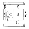
- FIG. 6 shows a possible embodiment of the interface structure of a VPU for integration into a system similar FIG. 5 ,
- the VPU is assigned a memory / DMA and / or IO interface for data transfer (0601), another system interface (0602) takes over the sequence control, such as the management of interrupts, the start / stop of the processing, the exchange of error states , Etc..
- the memory / DMA and / or IO interface is connected to a memory bus and / or IO bus.
- the system interface is preferably connected to an IO bus, but may alternatively or additionally be connected to a memory in accordance with 0511.
- the interfaces (0601, 0402) can be used to adapt different operating frequencies of the CPU and / or VPU and / or System can be configured, for example, the system or the CPU with eg 500MHz currently working and the VPU with 200MHz.
- the interfaces can perform a translation of the bus protocols, for example, the VPU internal protocol can be converted to an external AMBA bus protocol. They thus effect bus protocol translation means and / or are designed for bus protocol translation, in particular the bus protocol translation between internal VPU protocol and known bus protocol. It is also possible to provide a conversion directly to CPU internal bus protocols.
- the memory / DMA and / or IO interface supports the memory access of the CT to an external memory, which preferably takes place directly (memory mapped).
- the data transfer of the CT (s) and / or PAC (s) can be buffered, eg via FIFO stages.
- External memory can be directly addressed and addressed, furthermore DMA internal and / or external DMA transfers can be carried out.
- the system interface controls data processing, such as initialization and / or configuration startup. Furthermore, status and / or error conditions are exchanged. Interrupts for the control and synchronization between the CT's and a CPU can be supported.
- the system interface can convert VPU-internal protocols in such a way that they are converted to external (standard) protocols (eg AMBA).
- AMBA external (standard) protocols
- a preferred method of code generation for the described system is described in other parts of this application.
- the method describes a compiler that breaks program code into code for a CPU and code for a VPU.
- the decomposition is performed on the different processors.
- the respective decomposed codes are extended by the interface routines for communication between CPU and VPU. The extension can be done automatically by the compiler.
- the following tables show exemplary communications between a CPU and a VPU.
- the respective active functional units are assigned to the columns: CPU, system DMA and DMA interface (EDMA) or memory interface (memory I / F), system interface (system I / F, 0602), CTs, as well as the PAC.
- EDMA system DMA and DMA interface
- memory I / F system interface
- system I / F system interface
- CTs as well as the PAC.
- K1 references a configuration to be executed 1.
- the first table shows a flow when using system DMA (EDMA) for data transfer: CPU EDMA System I / F CT's PAC Initiate K1 Load K1 Start K1 Configure K1 Initiate load the data via EDMA Start K1 Waiting for data Initiate read the data via EDMA Data transfer read the data data processing Data transfer write the data Signal the end of the operation
- EDMA system DMA
- a preferred optimized sequence is shown.
- the VPU itself has direct access to the configuration memory (0306).
- the data transfers are performed by DMA circuitry within the VPU, which may, for example, be fixedly implemented and / or result from the configuration of configurable parts of the PAC.
- the present invention is concerned with methods that enable translation of a classical high level language such as Pascal, C, C ++, Java, etc. to a reconfigurable architecture.
- the method is designed such that only the parts of the program to be translated that are suitable for the reconfigurable target architecture are extracted. The remaining parts of the program are translated to a conventional processor architecture.
- a preferred implementation, such as in FIG. 1 shown can provide different data transfers between a CPU (0701) and VPU (0702).
- the configurations to be executed on the VPU are selected by the instruction decoder (0705) of the CPU, which recognizes certain instructions destined for the VPU and drives the CT (0706) to determine the corresponding configurations from a memory (0707) associated with the CT especially with the CPU or the same as the main memory the CPU can be loaded into the array of PAEs (PA, 0108).
- CPU registers (0703) are provided to extract, process, and write back to a CPU register upon registering.
- a status register (0704) is provided.
- a cache is provided which is intended to be used when exchanging data which has just been processed by the CPU, which are presumably still in the cache (0709) of the CPU or are subsequently processed by the CPU immediately afterwards.
- the external bus is designated (0710) and is read therefrom, for example, from a data source (e.g., memory, peripherals) associated therewith, or written to the external bus and associated data sink (e.g., memory, peripheral).
- a data source e.g., memory, peripherals
- this bus may be the same as the CPU's external bus (0712 & dashed).
- a cache-bus protocol (0711) is implemented which provides for correct contents of the cache.
- Denoted by (0713) is an FPGA (0713) which may be coupled to the VPU to enable fine-grained data processing and / or a flexible adaptable interface (0714) (eg, various serial interfaces (V24, USB, etc.), various parallel interfaces, hard disk interfaces, Ethernet, telecommunication interfaces (a / b, T0, ISDN, DSL, etc)) to further modules and / or the external bus system (0712).
- the operating system memory area is a table or linked list (LINKLIST, 0801) that points to all VPUCALL tables (0802) in the order of their creation.
- Also described above is a method, in particular for the translation of programs onto a system, consisting of a processor and a reconfigurable unit, wherein the code parts suitable for the reconfigurable unit are extracted and the remaining code is extracted by means of a any ordinary, unmodified, suitable for the processor compiler is translatable.
- a device for data processing has been described with at least one conventional processor and at least one reconfigurable unit, wherein a means for exchanging information, in particular data and status information, between the conventional processor and reconfigurable unit is provided, wherein the means is designed such that a Exchange of data and status information between them during the execution of one or more programs is possible and / or in particular without the data processing on the reconfigurable processor and / or the conventional processor must be significantly interrupted.
Abstract
Description
- Die vorliegende Erfindung befaßt sich mit Datenverarbeitung. Insbesondere befaßt sich die vorliegende Erfindung mit herkömmlichen, d.h. konventionellen und rekonfigurierbaren Prozessorarchitekturen sowie mit Verfahren hierfür, die eine Übersetzung einer klassischen Hochsprache (PROGRAMM) wie Pascal, C, C++, Java, etc. ermöglichen, insbesondere auf eine rekonfigurierbare Architektur. Insbesondere befaßt sich die vorliegende Erfindung mit der Integration und/oder engen Kopplung von rekonfigurierbaren Prozessoren mit Standardprozessoren, dem Datenaustausch und der Synchronisation der Datenverarbeitung.
- Unter einer konventionellen Prozessorarchitektur (PROZESSOR) werden vorliegend beispielsweise sequentielle Prozessoren mit einer von-Neumann- oder Harvardarchitektur verstanden, wie z.B. Kontroller, CISC-, RISC-, VLIW-, DSP-, u.ä. Prozessoren verstanden.
- Unter einer rekonfigurierbaren Zielarchitektur werden vorliegend Bausteine (VPU) mit wiederholt und insbesondere zur Laufzeit insbesondere unterbrechungsfrei konfigurierbarer Funktion und/oder Vernetzung verstanden, insbesondere integrierte Bausteine mit einer Mehrzahl von ein- oder mehrdimensional angeordneten arithmetischen und/oder logischen und/oder analogen und/oder speichernden insbesondere evtl. auch grobgranularen Baugruppen (PAE), die direkt oder durch ein Bussystem miteinander verbunden sind.
- Zur Gattung dieser Bausteine zählen insbesondere systolische Arrays, neuronale Netze, Mehrprozessor Systeme, Prozessoren mit mehreren Rechenwerken und/oder logischen Zellen, Vernetzungs- und Netzwerkbausteine wie z.B. Crossbar-Schalter, ebenso wie bekannte Bausteine der Gattung FPGA, DPGA, XPUTER, etc.. Hingewiesen wird insbesondere in diesem Zusammenhang auf die folgenden Schutzrechte desselben Anmelders: P 44 16 881.0-53,
DE 197 81 412.3 ,DE 197 81 483.2 ,DE 196 54 846.2-53 ,DE 196 54 593.5-53 ,DE 197 04 044.6-53 ,DE 198 80 129.7 ,DE 198 61 088.2-53 ,DE 199 80 312.9 ,PCT/DE 00/01869 ,DE 100 36 627.9-33 ,DE 100 28 397.7 ,DE 101 10 530.4 ,DE 101 11 014.6 ,PCT/EP 00/10516 ,EP 01 102 674.7 DE 196 51 075.9-53 ,DE 196 54 846.2-53 ,DE 196 54 593.5-53 ,DE 197 04 728.9 ,DE 197 07 872.2 ,DE 101 39 170.6 ,DE 199 26 538.0 ,DE 101 42 904.5 ,DE 101 10 530.4 . Diese sind hiermit zu Offenbarungszwecken vollumfänglich eingegliedert. - Das System kann insbesondere als (Standard)-Prozessor oder Baugruppe ausgestaltet sein und/oder in einem Halbleiter (System on Chip SoC) integriert sein.
- Rekonfigurierbare Bausteine (VPUs) unterschiedlicher Gattungen (wie z.B. PACT XPP-Technologie, Morphics, Morphosys, Chameleon) sind zu bestehenden technischen Umgebungen und Programmierverfahren weitgehend inkompatibel.
- Programme für diese Bausteine sind typisch inkompatibel zu bereits bestehenden Programmen von CPUs. Dadurch wird ein erheblicher Entwicklungsaufwand zur Programmierung erforderlich, z.B. besonders für Bausteine der Gattungen Morphics, Morphosys. Chameleon integriert bereits einen Standardprozessor (ARC) auf mehr oder minder rekonfigurierbaren Bausteinen. Dadurch stehen Ansätze für Tools zur Programmierung zur Verfügung. Allerdings ist nicht jede technische Umgebung für den Einsatz von ARC-Prozessoren geeignet, insbesondere liegen bestehende Programme, Codebibliotheken etc. oftmals für beliebige unbestimmte andere CPUs vor.
- Es hat sich in internen Versuchen gezeigt, daß es bestimmte Verfahren und Programmabläufe gibt, die sich besser mit einer rekonfigurierbare Architektur abarbeiten lassen als mit einer konventionellen Prozessorarchitektur. Umgekehrt gibt es auch solche Verfahren und Programmabläufe, die besser mit einer konventionellen Prozessorarchitektur ausgeführt werden können. Es ist dafür wünschenswert, um eine jeweilige Optimierung zu ermöglichen, eine Ablaufteilung vorzusehen.
- Bekannte Übersetzungsverfahren für rekonfigurierbare Architekturen unterstützen keine Weitergabe von Codes an beliebige Standard-Compiler zur Generierung von Objektcodes für einen beliebigen PROZESSOR. Gewöhnlicherweise ist der PROZESSOR fest innerhalb des Compilers definiert.
- Weiterhin existieren keine Scheduling-Mechanismen zur Rekonfiguration der einzelnen generierten Konfigurationen für VPUs. Insbesondere fehlen Scheduling-Mechanismen für die Konfiguration unabhängiger extrahierter Teile gleichwohl wie für einzelne Partitionen extrahierter Teile. Entsprechende Übersetzungsverfahren nach dem Stand der Technik sind beispielsweise definiert durch die Dissertation "Übersetzungsmethoden für strukturprogrammierbare Rechner, Dr. Markus Weinhardt, 1997".
- Zur Partitionierung von Array-CODE sind mehrere Verfahren nach dem Stand der Technik bekannt, z. B. Joao M. P. Cardoso, "Compilation of Java™ Algorithms onto Reconfigurable Computing Systems with Exploitation of Operation-Level Parallelism", Ph. D. Thesis Universidade Técnica de Lisboa (UTL), 2000.
- Diese Verfahren sind jedoch in keine kompletten Compilersysteme eingebettet. Weiterhin setzen die Verfahren die vollständige Steuerung der Rekonfiguration durch einen Hostprozessor voraus, was einen erheblichen Aufwand bedeutet. Die Partitionierungsstrategien sind für FPGA-basierende Systeme ausgelegt und entsprechen daher keinem echten Prozessormodell.
- Die Aufgabe dieser Erfindung besteht darin, Neues für die gewerbliche Anwendung bereitzustellen.
- Die Lösung dieser Aufgabe wird in unabhängiger Form beansprucht. Bevorzugte Ausführungen finden sich in den Unteransprüchen.
- Ein rekonfigurierbarer Prozessor (VPU) wird somit in eine technische Umgebung eindesigned, die einen Standardprozessor (CPU) besitzt, wie beispielsweise einen DSP, RISC, CISC-Prozessor oder (Mikro)-Kontroller aufweist. Das Design kann erfindungsgemäß derart erfolgen, dass eine einfache und leistungsfähige Anbindung besteht. Ein sich ergebender Aspekt ist die einfache Programmierbarkeit des entstehenden Systems. Die Weiterverwendung bestehender Programme der CPU sowie die Codekompatibilität und die einfache Integration der VPU in die bestehenden Programme finden Berücksichtigung.
- Eine VPU (oder ohne jeweils besonders erwähnt zu werden, mehrere VPUs) wird derart mit einer bevorzugten CPU (oder ohne jeweils besonders erwähnt zu werden, mehreren CPUs) gekoppelt, dass sie die Stelle und Funktion eines Coprozessors (bzw. mehrerer wahlweise ansprechbarer Coprozessoren) einnimmt. Die Funktion ermöglicht die einfache Einbindung in bestehende Programmcodes entsprechend den bereits existierenden Methoden zum Umgang mit Coprozessoren nach dem Stand der Technik.
- Der erfindungsgemäße Datenaustausch zwischen CPU und VPU kann mittels Speicherkopplung und/oder IO-Kopplung erfolgen. CPU und VPU können sämtliche Ressourcen teilen, in besonderen Ausgestaltungen ist es auch möglich, dass CPU und VPU nur einen Teil der Ressourcen gemeinsam verwenden und andere Ressourcen jeweils explizit und/oder exclusive für eine CPU oder VPU zur Verfügung stehen.
- Um einen Datenaustausch durchzuführen, können Datensätze und/oder Konfigurationen in jeweils besonders dafür vorgesehen Speicherbereiche kopiert bzw. geschrieben/gelesen werden und/oder entsprechende Basisadressen gesetzt werden, dass diese auf die jeweiligen Datenbereiche zeigen.
- Zur Steuerung des Coprozessors wird bevorzugt ein Datensatz vorgesehen, der beispielsweise die Grundeinstellungen einer VPU beeinhaltet, wie beispielsweise bestimmte Basisadressen. Desweiteren können Statusvariablen zur Ansteuerung und Funktionssteuerung einer VPU durch eine CPU sowie für Rückmeldungen einer VPU an eine CPU vorgesehen sein. Der Datensatz kann über einen gemeinsamen Speicher (RAM) und/oder über einen gemeinsamen peripheren Adressraum (IO) ausgetauscht werden.
- Zur Synchronisation der CPU und VPU können einseitig oder gegenseitig wirkende Interruptverfahren (die z.B. durch Signaltransfer über insbesondere dedizierte bzw. hierfür ausgebildete Interruptleitungen und/oder Interrupteingänge realisiert sind) vorgesehen sein und/oder die Synchronisation erfolgt mittels Pollingverfahren. Weiterhin können Interrupts zur Synchronisation von Daten- und/oder DMA-Transfers verwendet werden.
- In einer besonders zu bevorzugenden Ausgestaltung wird eine VPU durch eine CPU gestartet und arbeitet danach bevorzugt unabhängig die Applikation ab.
- Besonders leistungsfähig ist ein bevorzugter Aufbau, bei welchem die verwendete VPU eigene Mechanismen zum Laden und Kontrollieren von Konfigurationen vorsieht. Zur Gattung dieser VPUs gehören beispielsweise PACT XPP und Chameleon. Die erfindungsgemäßen Schaltungen ermöglichen ein Verfahren zum Betrieb derart, dass die Konfigurationen der VPU zusammen mit dem auszuführenden Programm der CPU in einen Speicher geladen werden. Die CPU kann während der Ausführung des Programms die VPU auf die Speicherstellen verweisen (z.B. durch Angabe der Adressen oder Pointer), die die jeweils auszuführenden Konfigurationen beinhalten. Die VPU kann daraufhin die Konfigurationen selbständig und ohne weitere Einflussnahme durch die CPU laden. Die Ausführung startet sofort oder ggf. durch eine zusätzliche Information (z.B. Interrupt und/oder Start Befehl) durch die CPU.
- In einer besonders bevorzugten Erweiterung kann die VPU selbständig innerhalb eines Speichers Daten lesen und schreiben.
- In einer besonders bevorzugten Erweiterung kann die VPU ebenfalls selbständig neue Konfigurationen aus dem Speicher laden und sich bei Bedarf neu konfigurieren, ohne dass es eines weiteren Einflusses durch die CPU bedarf.
- Diese Ausgestaltungen ermöglichen einen weitestgehend von CPUs unabhängigen Betrieb von VPUs. Lediglich ein Synchronisationsaustausch zwischen CPU und VPU, der bevorzugt bidirektional stattfinden kann, sollte zusätzlich vorgesehen werden, um die Datenverarbeitungen und/oder Konfigurationsausführungen aufeinander abzustimmen.
- Es wurde weiter erkannt, daß Verfahren zur Datenverarbeitung bevorzugt so ausgelegt werden können und/oder sollen, daß jeweils für die rekonfigurierbare Zielarchitektur (VPU) besonders geeignete Teile (VPU-CODE) des zu übersetzenden Programmes identifiziert und extrahiert werden, um eine besonders effiziente Datenverarbeitung zu ermöglichen. Diese Teile sind entsprechend zu partitionieren und die Konfiguration der einzelnen Partitionen ist in ihrer zeitlichen Reihenfolge zu steuern.
- Die verbleibenden Teile des Programms können auf eine konventionelle Prozessorarchitektur (PROZESSOR) übersetzt werden. Dies geschieht bevorzugt dergestalt, daß diese Teile als Hochsprachencode in einer Standard-Hochsprache (z. B. ANSI C) derart ausgegeben werden, daß ein gewöhnlicher (ggf. bereits existierender) Hochsprachencompiler diese ohne weiteres verarbeiten kann.
- Weiterhin sei angemerkt, daß die Verfahren auch auf Gruppen von mehreren Bausteinen angewendet werden können.
- Insbesondere kann eine Art "Double-Buffering" zur besonders einfachen und zugleich schnellen Rekonfiguration angewendet werden, in welchem eine Mehrzahl von VPUs vorgesehen sind, wobei ein Teil der VPUs zu einer Zeit rekonfiguriert werden kann, zu welcher ein anderer Teil rechnet und möglicherweise ein Weiterer etwa inaktiv sein kann. Die Daten-, Trigger-, Statusverbindungen etc. werden zwischen der Mehrzahl von VPUs geeignet ausgetauscht und ggf. durch adressierte Busse und/oder Multiplexer/Demultiplexer entsprechend der aktuell aktiven und/oder zu rekonfigurierenden VPUs verschaltet.
- Ein Vorteil dieses Verfahrens liegt darin, daß bestehender Code, der für einen beliebigen PROZESSOR geschrieben wurde, unter Einbeziehung einer VPU weiterverwendet werden kann und keine oder nur vergleichsweise geringe Modifikationen durchgeführt werden müssen. Die Modifikationen können zudem schrittweise erfolgen, wobei nach und nach immer mehr Code von dem PROZESSOR auf die VPU übertragen werden kann. Das Projektrisiko sinkt und die Überschaubarkeit steigt wesentlich an. Es wird darauf hingewiesen, daß einer derartigen sukzessive Übertragung von immer mehr Aufgaben auf die VPU, d.h. auf das integrale multidimensionale partiell rekonfigurierbaren insbesondere grobgranulare Feld an Elementen, eine besondere Bedeutung für sich hat und für sich als erfinderisch angesehen wird aufgrund seiner gravierenden Vorteile bei der Systemportierung.
- Weiterhin kann der Programmierer in seiner gewohnten Entwicklungsumgebung arbeiten und muß sich nicht auf eine neue, möglicherweise fremde Entwicklungsumgebung einstellen.
- Ein erster wesentlicher Aspekt der vorliegenden Erfindung ist darin zu sehen, daß ein PROZESSOR derart mit einer oder mehreren VPU(s) verbunden wird, daß ein effizienter Informationsaustausch, insbesondere in Form von Daten- und Statusinformation möglich ist.
- Der Anordnung eines herkömmlichen Prozessors und eines rekonfigurierbaren Prozessors, dergestalt, daß ein Austausch von Daten- und/oder Statusinformation zwischen denselben während der Abarbeitung eines oder mehrerer Programme möglich ist und/oder ohne daß insbesondere die Datenverarbeitung auf dem rekonfigurierbaren Prozessor und/oder dem herkömmlichen Prozessor signifikant unterbrochen werden muß, sowie der Ausbildung eines derartigen Systems, wird gleichfalls für sich Bedeutung zugemessen.
- Es können zunächst beispielsweise eines oder alle der folgenden Verbindungsverfahren und/oder -mittel verwendet werden:
- a) Shared-Memory
- b) Netzwerk (beispielsweise Bussysteme wie z.B. PCI-Bus, Serielle Busse wie z.B. Ethernet)
- c) Kopplung an einen internen Registersatz oder mehrere interne Registersätze
- d) andere Speichermedien (Festplatte, Flash-ROM, etc.)
- Prinzipiell kann auch die VPU und/oder CPU selbständig ohne Zuhilfenahme eines DMAs auf den Speicher zugreifen. Der gemeinsame Speicher kann insbesondere auch als Dualport- oder Multiportspeicher ausgestaltet sein. Dem System können weitere
Baugruppen zugeordnet werden, insbesondere können rekonfigurierbare FPGAs eingesetzt werden, um eine feingranulare Verarbeitung von einzelner Signale oder Datenbits zu ermöglichen und/oder flexible adaptierbare Interface (z.B. diverse serielle Schnittstellen (V24, USB, etc.), diverse parallele Schnittstellen, Festplattenschnittstellen, Ethernet, Telekommunikationsschnittstellen (a/b, T0, ISDN, DSL, etc.)) aufbauen zu können. - Der Aufbau einer VPU ist beispielsweise bekannt aus den o. g. zitierten Anmeldungen. Versuche zu alternativen Bausteindefinitionen sind beispielsweise unter dem Namen Chameleon geführt worden. VPUs lassen sich auf unterschiedliche Weise in ein System integrieren. Ein Anschluß an einen Hostprozessor ist beispielsweise möglich. Je nach Verfahren kann der Hostprozessor die Konfigurationskontrolle (HOSTRECONF) mit übernehmen (z. B. Chameleon) oder, z. B., eine dedizierte Einheit (CT) zur Steuerung der (Re)Konfiguration bestehen.
- Entsprechend generiert der Übersetzer gemäß dem beschriebenen Verfahren die Steuerinformation für die Rekonfiguration für eine CT und/oder einen HOSTRECONF.
- Es kann nun das Übersetzungsprinzip derart ausgestaltet sein, daß aus einem PROGRAMM mittels eines PRÄPROZESSORS die Teile extrahiert werden, die sich auf die jeweils bestimmte(n) VPU(s) effizient und/oder sinnvoll abbilden lassen. Diese Teile werden in ein für VPUs geeignetes Format transformiert (NML) und dann weiter in einen Objektcode übersetzt.
- Der verbleibenden Code und/oder der extrahierte Code wird erfahrungsgemäß an oder bezüglich der Stelle der durch die Extraktion fehlenden Code-Teile um einen Interface-Code erweitert, der entsprechend der Architektur des Zielsystems die Kommunikation zwischen PROZESSOR(en) und VPU(s) steuert. Der verbleibende und ggf. erweiterte Code kann bevorzugt trahiert werden sollen. Beispielsweise kann dies folgendermaßen erfolgen:
    ...
    Code
    ...
    # START_EXTRACTION
    Zu extrahierender Code
    # END_EXTRACTION
    ...
    Code
    ...
   // START_EXTRACTION" kennzeichnet den Beginn eines zu extra-
 hierenden Codes.
    // END_EXTRACTION" kennzeichnet das Ende eines zu extrahie-
 renden Code.
- a) NML-Code
...
procedure EXAMPLE
begin
...
end
... - b) PROGRAMM Code
...
Code
...
call EXAMPLE // Aufruf des NML-Codes
...
Code
...
- a) Klassen-Code
...
class EXAMPLE
begin
...
end
... - b) PROGRAMM Code
...
Code
...
EXAMPLE var() // Instantiierung der Klasse
...
Code
...
Diese Teile werden aus dem PROGRAMM extrahiert.
Beispielsweise können folgende Datentypen bestehen:
- TYPE stream1 of Byte [];
- TYPE stream2 of Byte [0..255;
Der FPGA kann dabei aus der VPU-Architektur, insbesondere durch die CT, und/oder durch die CPU konfiguriert werden. Der FPGA kann statisch, also ohne Rekonfiguration zur Laufzeit und/oder dynamisch, also mit Rekonfiguration zur Laufzeit, betrieben werden.
- a) Der Interface-Code kann vom Lieferanten des Compilers für bestimmte Verbindungsverfahren zwischen VPU und CPU(s) vorgegeben werden. Dies kann bei der Organisation der Datenbank berücksichtigt werden, indem entsprechende Speichermittel für diese Angaben bereitgehalten werden.
- b) Der Interface-Code kann vom Benutzer, der den Systemaufbau bestimmt hat, selbst geschrieben oder aus bestehenden (Beispiel-) Interface-Code modifiziert und der Datenbank zugefügt werden. Das Datenbankmittel wird hierzu bevorzugt benutzermodifizierbar gestaltet, um dem Benutzer die Datenbankmodifikation zu ermöglichen.
- c) Der Interface-Code kann von eine Entwicklungssystem, mit dem beispielsweise der Systemaufbau des VPU-CPU-Systems geplant und/oder beschrieben und/oder getestet wurde, automatisch generiert werden.
Es ist daher also möglich und bevorzugt, derartige Abläufe durch das Einfügen von Steuercodes für Debugger und/oder Entwicklungssysteme in den Interface-Code abzuwickeln.
 while TRUE
      s := 0
      for i: 1 to 3
          s := s + inputstream;
Die Beendigung einer Datenverarbeitung wird durch das Eintreffen des Terminierungssignal (TERM) in einem Statusregister signalisiert. Die Terminierungssignale treffen in der Reihenfolge einer möglichen Verarbeitungspipeline ein.
- Ein einfach zu realsierenden Ansatz ist, die Datensynchronisation über ein Statusregister durchzuführen. Beispielsweise kann die VPU das erfolgte Auslesen von Daten aus einem Register und das damit verbundene ACK-Signal und/oder das Einschreiben von Daten in ein Register und das damit verbundene RDY-Signal in dem Statusregister anzeigen. Die CPU testet zunächst das Statusregister und führt beispielsweise so lange Warteschleifen oder Taskwechsel aus, bis - je nach Operation - das RDY oder ACK eintraf. Danach führt die CPU den jeweiligen Registerdatentransfer aus.
- Jeder Task generiert zum Aufruf der VPU eine oder mehrere Tabelle(n) (VPUCALL) mit einem geeigneten festgelegten Datenformat in dem ihm zugewiesenen Speicherbereich. Diese Tabelle beeinhaltet sämtliche Steuerinformation für eine VPU, wie z.B. das auszuführende Programm / die auszuführende Konfiguration und/oder Zeiger auf die Speicherstelle(n) oder Datenquellen der Eingangsdaten und/oder die Speicherstelle(n) oder Datensenken der Ergebnisdaten und/oder weitere Ausführungsparameter, z.B. Datenarraygrößen.
Sofern sichergestellt ist, daß eine Konfiguration - die der Abarbeitung eines Tasks entspricht - nur nach der kompletten Abarbeitung - d.h. wenn alle innerhalb dieses Konfigurationszyklusses zu bearbeitende Daten und Zustände gespeichert sind - terminiert, können lokal relevante Zustände ungespeichert bleiben.
Sofern der Task-Scheduler allerdings Konfigurationen vor deren vollständiger Abarbeitung abbricht, müssen lokale Zustände und/oder Daten gespeichert werden. Weiterhin ist dies von Vorteil, wenn die Abarbeitungszeit einer Konfiguration nicht vorhergesagt werden kann. In Verbindung mit dem bekannten Halteproblem und dem Risiko, daß eine Konfiguration (z.B. durch einen Fehler) gar nicht terminiert, erscheint dies weiterhin sinnvoll, um damit einen Deadlock des gesamten Systems zu verhindern.
Mit anderen Worten sind, unter Berücksichtung von Taskwechseln, relevante Zustände auch als solche anzusehen, die für einen Taskwechsel und ein erneutes korrekes Aufsetzen der Datenverarbeitung notwendig sind.
Bei einem Taskswitch ist somit der Speicher für Ergebnisse und ggf. auch der Speicher für die Operanden zu sichern und zu einem späteren Zeitpunkt, also bei der Rückkehr zu diesem Task, wieder herzustellen. Dies kann vergleichbar zu den PUSH/POP Befehlen und Verfahren nach dem Stand der Technik erfolgen. Weiterhin ist der Zustand der Datenverarbeitung zu sichern, also der Zeiger auf die zuletzt vollständig bearbeiteten Operanden. Es sei hier besonders auf PACT18 verwiesen.
Abhängig von der Optimierung des Taskswitches gibt es beispielsweise zwei Möglichkeiten:
- a) Die abgebrochene Konfiguration wird neu konfiguriert und nur die Operanden werden geladen. Die Datenverarbeitung beginnt von neuem, als ob die Bearbeutung der Konfiguration noch gar nicht begonnen wurde. Mit anderen Worten werden einfach alle Datenberechnungen von vorne an ausgeführt, wobei ggf. Berechnungen bereits zuvor durchgeführt wurden. Diese Möglichkeit ist einfach aber nicht sehr effizient.
- b) Die abgebrochene Konfiguration wird neu konfiguriert, wobei die Operanden und bereits berechneten Ergebnisse in die jeweiligen Speicher geladen werden. Die Datenverarbeitung wird bei den Operanden fortgesetzt die nicht mehr vollständig berechnet wurden. Dieses Verfahren ist sehr viel effizienter, setzt aber voraus, daß ggf. zusätzliche Zustände, die während der Verarbeitung der Konfiguration entstehen, relevant werden, beispielsweise muß zumindest ein Zeiger auf die zuletzt vollständig verrechneten Operanden gesichert werden, damit bei deren Nachfolgern nach erfolgter neuer Konfiguration neu aufgesetzt werden kann.
Eine zweite Konfiguration wird geladen, diese verbindet die REG in geeigneter Weise und definierter Reihenfolge mit einem oder mehreren globalen Speicher(n).
Die Konfiguration kann beispielsweise Adressgeneratoren verwenden um auf den/die globalen Speicher zuzugreifen.
Die Konfiguration kann beispielsweise Adressgeneratoren verwenden um auf als Speicher ausgestaltete REG zuzugreifen. Entsprechend der konfigurierten Verbindung zwischen den REG werden die Inhalte der REG in einer definierten Reihenfolge in den globalen Speicher geschrieben, wobei die jeweiligen Adressen von Adressgeneratoren vorgegeben werden. Der Adressgenerator generiert die Adressen für den/die globalen Speicher derart, dass die beschriebenen Speicherbereiche (PUSHAREA) der entfernten ersten Konfiguration eindeutig zugeordnet werden können.
Mit anderen Worten, es sind bevorzugt für unterschiedliche Konfigurationen unterschiedliche Adressenräume vorgesehen. Die Konfiguration entspricht einem PUSH gewöhnlicher Prozessoren.
 proc example
  while i<length do
     x[i] = a[i] + b[i]
Dazu wird die Konfiguration example terminiert, wobei die Registerinhalte erhalten bleiben und eine Konfiguration push gestartet, die i und length aus den Registern liest und in einen Speicher schreibt.
 proc push
  mem[<push_adr_example>] = i
  push_adr_example++
  mem[<push_adr_example>] = length
Andere Konfigurationen werden ausgeführt. Nach einiger Zeit wird die Konfiguration example wieder gestartet.
Zuvor wird eine Konfiguration pop gestartet, die die Registerinhalte wieder aus dem Speicher liest.
 proc pop
  i = mem[<push_adr_example>]
  push_adr_example++
  length = mem[<push_adr_example>]
-
Figur 1 verdeutlicht ein Beispiel das vorgeschlagene Verfahren und zeigt einen möglichen Systemaufbau. Dabei ist ein PROZESSOR (0101) über ein geeignetes Interface (0102) zum Daten- und Statusaustausch mit einer VPU (0103) verbunden. Ein PROGRAMM-Code (0110) wird (z. B. durch einen Präprozessor für einen Compiler) beispielsweise gemäß den beschriebenen Extraktionsmethoden in einen für den PROZESSOR geeigneten Teil (0111) und einen VPU-geeigneten Teil (0112) zerlegt.
Der Standard-Compiler kann dergestalt sein, daß er als marktübliches Werkzeug oder im Rahmen einer marktüblichen Entwicklungsumgebung vorliegt. Der Präprozessor und/oder möglicherweise der VPU-Compiler und/oder möglicherweise der Debugger und weitere Werkzeuge können beispielsweise in eine bestehende marktübliche Entwicklungsumgebung integriert werden.
Der entstandene Code wird auf seine Performance analysiert (0214), ggf. ist eine Rückkopplung (0215) auf die Extraktion möglich, um Verbesserungen durch eine geänderte Zuordnung der Codes zum PROZESSOR oder einer VPU zu erhalten.
Der entstandene VPU-Code (0216) wird für eine weitere Übersetzung an einen nachgeschalteten für die VPU geeigneten Compiler weitergegeben. Der entstandene PROZESSOR-Code (0217) wird für die weitere Übersetzung in einem beliebigen nachgeschalteten für den PROZESSOR geeigneten Compiler weiterverarbeitet.
Typischerweise und bevorzugt weist eine vollausgestaltete VPU eigene Adressgeneratoren und/oder DMAs auf um Datentransfers durchzuführen. Alternativ und/oder zusätzlich ist es möglich, dass ein DMA (0507) innerhalb des Systems (
- 1. Basisadresse(n) des CT-Speicherbereiches in 0506 zur Lokalisierung der Konfigurationen.
- 2. Basisadresse(n) von Datentransfers mit 0505.
- 3. IO Adressen von Datentransfers mit 0508.
- 4. Synchronisationsinformation, z.B. Zurücksetzen, anhalten, starten der VPU.
- 5. Statusinformation der VPU, z.B. Fehler oder Zustand der Datenverarbeitung.
Das Speicher/DMA- und/oder IO-Interface wird an einen Speicherbus und/oder IO-Bus angeschlossen.
Über das System-Interface erfolgt die Steuerung der Datenverarbeitung, wie beispielsweise die Initialisierung und/oder der Start von Konfigurationen. Des weiteren werden Status und/oder Fehlerzustände ausgetauscht. Interrupts für die Steuerung und Synchronisation zwischen den CT's und einer CPU können unterstützt werden.
| CPU | EDMA | System-I/F | CT's | PAC |
| Initiiere K1 | ||||
| Lade K1 | ||||
| Starte K1 | Konfiguriere K1 | |||
| Initiiere laden der Daten per EDMA | Starte K1 | Warten auf Daten | ||
| Initiiere lesen der Daten per EDMA | Datentransfer lesen der Daten | Datenverarbeitung | ||
| Datentransfer schreiben der Daten | Signalisiere Ende der Operation |
| CPU | EDMA | System-I/F | CT's | PAC |
| Initiiere K1 | ||||
| Starte K1 | Lesen der Konfiguration | Konfiguriere K1 | ||
| Datentransfer lesen der Daten | Starte K1 | Lese Daten | ||
| Datenverarbeitung | ||||
| Datentransfer schreiben der Daten | Signalisiere Ende der Operation | Schreibe Daten |
Claims (3)
- Verfahren zur Ausführung von Programmen auf einem System, bestehend aus
wenigstens einem ersten Prozessor und
einer rekonfigurierbaren Einheit, dieein rekonfigurierbares Array undeinen diesem zugeordneten Konfigurationsmanager umfasst sowieeinen Task-Scheduler,wobei die Ausführung den Wechsel von Tasks umfasst und
wobei bei zumindest einigen Taskwechseln zwischen auf der rekonfigurierbaren Einheit abzuarbeitenden Programmteilen ein Kontext-Switch erfolgt,
indem mittels des Konfigurationsmanagers unterschiedliche Konfigurationen nacheinander in die rekonfigurierbare Einheit einkonfiguriert werden und
wobei ein Kontext-Switch die Ausführung von Push- und/oder Pop-Konfigurationen umfasst, welche mittels der zugeordneten Konfigurationsmanager konfigurierbar sind,
wobei der Kontext-Switch von einer ersten auf eine zweite, nachfolgende Konfiguration derart ausgeführt wird, dasseine erste Konfiguration entfernt wird,zu sichernde Daten in den entsprechenden Registern verbleiben,eine Push-Konfiguration geladen wird, welche die entsprechenden Speicher in geeigneter Weise und definierter Reihenfolge mit globalem Speicher verbindet,und erst danach,gegebenenfalls nach Ausführung einer Pop-Konfiguration, welche Speicher in einer definierten Reihenfolge für die nachfolgend auszuführende Konfiguration verbindet,der Kontext-Switch auf die zweite Konfiguration erfolgt,so dass der Scheduler bei der Abarbeitung Tasks dem Prozessor oderder rekonfigurierbaren Einheit wie erforderlich zuweisen kann. - Verfahren nach dem vorhergehenden Anspruch, dadurch gekennzeichnet, dass zumindest eine der POP- und/oder PUSH-Konfigurationen Adressgeneratormittel zur Generierung von Adressen aufweist.
- Verfahren nach einem der vorhergehenden Ansprüche, dadurch gekennzeichnet, dass PUSH- und/oder POP-Konfigurationen Adressgeneratoren verwenden, um auf den globalen und/oder den entsprechenden Speicher zuzugreifen.
Priority Applications (1)
| Application Number | Priority Date | Filing Date | Title |
|---|---|---|---|
| EP10005502A EP2224330B1 (de) | 2001-06-20 | 2002-06-20 | Verfahren und gerät zum partitionieren von grossen rechnerprogrammen |
Applications Claiming Priority (33)
| Application Number | Priority Date | Filing Date | Title |
|---|---|---|---|
| EP01115021 | 2001-06-20 | ||
| DE10135210 | 2001-07-24 | ||
| DE10135211 | 2001-07-24 | ||
| DE10139170 | 2001-08-16 | ||
| DE10142231 | 2001-08-29 | ||
| DE10142894 | 2001-09-03 | ||
| DE10142903 | 2001-09-03 | ||
| DE10142904 | 2001-09-03 | ||
| DE10144732 | 2001-09-11 | ||
| DE10144733 | 2001-09-11 | ||
| DE10145795 | 2001-09-17 | ||
| DE10145792 | 2001-09-17 | ||
| DE10146132 | 2001-09-19 | ||
| DE10154259 | 2001-11-05 | ||
| DE10154260 | 2001-11-05 | ||
| EP01129923 | 2001-12-14 | ||
| EP02001331 | 2002-01-18 | ||
| DE10202044 | 2002-01-19 | ||
| DE10202175 | 2002-01-20 | ||
| DE10206653 | 2002-02-15 | ||
| DE10206856 | 2002-02-18 | ||
| DE10206857 | 2002-02-18 | ||
| DE10207224 | 2002-02-21 | ||
| DE10207226 | 2002-02-21 | ||
| DE10207225 | 2002-02-21 | ||
| DE10208435 | 2002-02-27 | ||
| DE10208434 | 2002-02-27 | ||
| DE10212622A DE10212622A1 (de) | 2002-03-21 | 2002-03-21 | Prozessorkopplung |
| DE10212621 | 2002-03-21 | ||
| EP02009868 | 2002-05-02 | ||
| EP10005502A EP2224330B1 (de) | 2001-06-20 | 2002-06-20 | Verfahren und gerät zum partitionieren von grossen rechnerprogrammen |
| DE10129237A DE10129237A1 (de) | 2000-10-09 | 2002-06-20 | Verfahren zur Bearbeitung von Daten |
| EP02780770A EP1402382B1 (de) | 2001-06-20 | 2002-06-20 | Verfahren zur bearbeitung von daten |
Related Parent Applications (1)
| Application Number | Title | Priority Date | Filing Date |
|---|---|---|---|
| EP02780770.0 Division | 2002-06-20 |
Publications (2)
| Publication Number | Publication Date |
|---|---|
| EP2224330A1 true EP2224330A1 (de) | 2010-09-01 |
| EP2224330B1 EP2224330B1 (de) | 2012-05-09 |
Family
ID=42676650
Family Applications (2)
| Application Number | Title | Priority Date | Filing Date |
|---|---|---|---|
| EP02780770A Expired - Lifetime EP1402382B1 (de) | 2001-06-20 | 2002-06-20 | Verfahren zur bearbeitung von daten |
| EP10005502A Expired - Lifetime EP2224330B1 (de) | 2001-06-20 | 2002-06-20 | Verfahren und gerät zum partitionieren von grossen rechnerprogrammen |
Family Applications Before (1)
| Application Number | Title | Priority Date | Filing Date |
|---|---|---|---|
| EP02780770A Expired - Lifetime EP1402382B1 (de) | 2001-06-20 | 2002-06-20 | Verfahren zur bearbeitung von daten |
Country Status (6)
| Country | Link |
|---|---|
| US (2) | US7657877B2 (de) |
| EP (2) | EP1402382B1 (de) |
| JP (1) | JP2004533691A (de) |
| AT (2) | ATE557344T1 (de) |
| AU (1) | AU2002347560A1 (de) |
| WO (1) | WO2002103532A2 (de) |
Families Citing this family (66)
| Publication number | Priority date | Publication date | Assignee | Title |
|---|---|---|---|---|
| US7266725B2 (en) * | 2001-09-03 | 2007-09-04 | Pact Xpp Technologies Ag | Method for debugging reconfigurable architectures |
| DE19654595A1 (de) * | 1996-12-20 | 1998-07-02 | Pact Inf Tech Gmbh | I0- und Speicherbussystem für DFPs sowie Bausteinen mit zwei- oder mehrdimensionaler programmierbaren Zellstrukturen |
| EP1329816B1 (de) * | 1996-12-27 | 2011-06-22 | Richter, Thomas | Verfahren zum selbständigen dynamischen Umladen von Datenflussprozessoren (DFPs) sowie Bausteinen mit zwei- oder mehrdimensionalen programmierbaren Zellstrukturen (FPGAs, DPGAs, o.dgl.) |
| US6542998B1 (en) | 1997-02-08 | 2003-04-01 | Pact Gmbh | Method of self-synchronization of configurable elements of a programmable module |
| US8686549B2 (en) * | 2001-09-03 | 2014-04-01 | Martin Vorbach | Reconfigurable elements |
| DE19861088A1 (de) * | 1997-12-22 | 2000-02-10 | Pact Inf Tech Gmbh | Verfahren zur Reparatur von integrierten Schaltkreisen |
| TW463528B (en) * | 1999-04-05 | 2001-11-11 | Idemitsu Kosan Co | Organic electroluminescence element and their preparation |
| JP2003505753A (ja) * | 1999-06-10 | 2003-02-12 | ペーアーツェーテー インフォルマツィオーンステヒノロギー ゲゼルシャフト ミット ベシュレンクテル ハフツング | セル構造におけるシーケンス分割方法 |
| DE50115584D1 (de) * | 2000-06-13 | 2010-09-16 | Krass Maren | Pipeline ct-protokolle und -kommunikation |
| US8058899B2 (en) | 2000-10-06 | 2011-11-15 | Martin Vorbach | Logic cell array and bus system |
| US7844796B2 (en) * | 2001-03-05 | 2010-11-30 | Martin Vorbach | Data processing device and method |
| US7444531B2 (en) * | 2001-03-05 | 2008-10-28 | Pact Xpp Technologies Ag | Methods and devices for treating and processing data |
| US9037807B2 (en) | 2001-03-05 | 2015-05-19 | Pact Xpp Technologies Ag | Processor arrangement on a chip including data processing, memory, and interface elements |
| US20090210653A1 (en) * | 2001-03-05 | 2009-08-20 | Pact Xpp Technologies Ag | Method and device for treating and processing data |
| US7996827B2 (en) * | 2001-08-16 | 2011-08-09 | Martin Vorbach | Method for the translation of programs for reconfigurable architectures |
| US7434191B2 (en) * | 2001-09-03 | 2008-10-07 | Pact Xpp Technologies Ag | Router |
| US8686475B2 (en) * | 2001-09-19 | 2014-04-01 | Pact Xpp Technologies Ag | Reconfigurable elements |
| WO2003060747A2 (de) | 2002-01-19 | 2003-07-24 | Pact Xpp Technologies Ag | Reconfigurierbarer prozessor |
| AU2003214003A1 (en) | 2002-02-18 | 2003-09-09 | Pact Xpp Technologies Ag | Bus systems and method for reconfiguration |
| US20110161977A1 (en) * | 2002-03-21 | 2011-06-30 | Martin Vorbach | Method and device for data processing |
| US8914590B2 (en) | 2002-08-07 | 2014-12-16 | Pact Xpp Technologies Ag | Data processing method and device |
| US7657861B2 (en) * | 2002-08-07 | 2010-02-02 | Pact Xpp Technologies Ag | Method and device for processing data |
| AU2003286131A1 (en) * | 2002-08-07 | 2004-03-19 | Pact Xpp Technologies Ag | Method and device for processing data |
| EP1537486A1 (de) | 2002-09-06 | 2005-06-08 | PACT XPP Technologies AG | Rekonfigurierbare sequenzerstruktur |
| DE112004000026D2 (de) * | 2003-04-04 | 2006-06-14 | Pact Xpp Technologies Ag | Verfahren und Vorrichtung für die Datenverarbeitung |
| US20070186076A1 (en) * | 2003-06-18 | 2007-08-09 | Jones Anthony M | Data pipeline transport system |
| EP1636725B1 (de) * | 2003-06-18 | 2018-05-16 | Imagination Technologies Limited | Register für einen integrierten schaltkreis und methode dafür |
| WO2006082091A2 (en) * | 2005-02-07 | 2006-08-10 | Pact Xpp Technologies Ag | Low latency massive parallel data processing device |
| EP1676208A2 (de) * | 2003-08-28 | 2006-07-05 | PACT XPP Technologies AG | Datenverarbeitungseinrichtung und verfahren |
| US7620162B2 (en) | 2004-08-27 | 2009-11-17 | At&T Intellectual Property I.L.P. | Methods, systems and computer program products for monitoring service usage |
| US7805708B2 (en) * | 2005-05-13 | 2010-09-28 | Texas Instruments Incorporated | Automatic tool to eliminate conflict cache misses |
| WO2007028226A1 (en) * | 2005-09-09 | 2007-03-15 | Ibm Canada Limited - Ibm Canada Limitee | Method and system for state machine translation |
| US20080216064A1 (en) * | 2005-09-29 | 2008-09-04 | William Braswell | Method, Architecture and Software of Meta-Operating System, Operating Systems and Applications For Parallel Computing Platforms |
| US7711990B1 (en) * | 2005-12-13 | 2010-05-04 | Nvidia Corporation | Apparatus and method for debugging a graphics processing unit in response to a debug instruction |
| US7600155B1 (en) * | 2005-12-13 | 2009-10-06 | Nvidia Corporation | Apparatus and method for monitoring and debugging a graphics processing unit |
| US8212824B1 (en) | 2005-12-19 | 2012-07-03 | Nvidia Corporation | Apparatus and method for serial save and restore of graphics processing unit state information |
| EP1974265A1 (de) * | 2006-01-18 | 2008-10-01 | PACT XPP Technologies AG | Hardwaredefinitionsverfahren |
| US9013494B2 (en) | 2006-12-07 | 2015-04-21 | Sony Computer Entertainment Inc. | Heads-up-display software development tool |
| US7950003B1 (en) * | 2006-12-07 | 2011-05-24 | Sony Computer Entertainment Inc. | Heads-up-display software development tool for analyzing and optimizing computer software |
| US8341612B2 (en) * | 2007-05-16 | 2012-12-25 | International Business Machines Corporation | Method and apparatus for run-time statistics dependent program execution using source-coding |
| US7739440B2 (en) * | 2007-08-16 | 2010-06-15 | Texas Instruments Incorporated | ATA HDD interface for personal media player with increased data transfer throughput |
| US8561037B2 (en) | 2007-08-29 | 2013-10-15 | Convey Computer | Compiler for generating an executable comprising instructions for a plurality of different instruction sets |
| US9710384B2 (en) * | 2008-01-04 | 2017-07-18 | Micron Technology, Inc. | Microprocessor architecture having alternative memory access paths |
| US9015399B2 (en) | 2007-08-20 | 2015-04-21 | Convey Computer | Multiple data channel memory module architecture |
| US8095735B2 (en) * | 2008-08-05 | 2012-01-10 | Convey Computer | Memory interleave for heterogeneous computing |
| US8156307B2 (en) * | 2007-08-20 | 2012-04-10 | Convey Computer | Multi-processor system having at least one processor that comprises a dynamically reconfigurable instruction set |
| US8122229B2 (en) * | 2007-09-12 | 2012-02-21 | Convey Computer | Dispatch mechanism for dispatching instructions from a host processor to a co-processor |
| DE112008003643A5 (de) * | 2007-11-17 | 2010-10-28 | Krass, Maren | Rekonfigurierbare Fliesskomma- und Bit- ebenen Datenverarbeitungseinheit |
| US20110173596A1 (en) * | 2007-11-28 | 2011-07-14 | Martin Vorbach | Method for facilitating compilation of high-level code for varying architectures |
| US8402438B1 (en) | 2007-12-03 | 2013-03-19 | Cadence Design Systems, Inc. | Method and system for generating verification information and tests for software |
| WO2009071329A1 (en) * | 2007-12-07 | 2009-06-11 | Pact Xpp Technologies Ag | Using function calls as compiler directives |
| US8434076B2 (en) * | 2007-12-12 | 2013-04-30 | Oracle International Corporation | Efficient compilation and execution of imperative-query languages |
| US8156474B2 (en) * | 2007-12-28 | 2012-04-10 | Cadence Design Systems, Inc. | Automation of software verification |
| US8504344B2 (en) * | 2008-09-30 | 2013-08-06 | Cadence Design Systems, Inc. | Interface between a verification environment and a hardware acceleration engine |
| US20100115233A1 (en) * | 2008-10-31 | 2010-05-06 | Convey Computer | Dynamically-selectable vector register partitioning |
| US8205066B2 (en) * | 2008-10-31 | 2012-06-19 | Convey Computer | Dynamically configured coprocessor for different extended instruction set personality specific to application program with shared memory storing instructions invisibly dispatched from host processor |
| US8463820B2 (en) * | 2009-05-26 | 2013-06-11 | Intel Corporation | System and method for memory bandwidth friendly sorting on multi-core architectures |
| GB2470589A (en) * | 2009-05-29 | 2010-12-01 | Vestas Wind Sys As | Branching spar wind turbine blade |
| WO2010142432A2 (en) | 2009-06-09 | 2010-12-16 | Martin Vorbach | System and method for a cache in a multi-core processor |
| US8423745B1 (en) | 2009-11-16 | 2013-04-16 | Convey Computer | Systems and methods for mapping a neighborhood of data to general registers of a processing element |
| US8701099B2 (en) * | 2010-11-02 | 2014-04-15 | International Business Machines Corporation | Accelerating generic loop iterators using speculative execution |
| US10430190B2 (en) | 2012-06-07 | 2019-10-01 | Micron Technology, Inc. | Systems and methods for selectively controlling multithreaded execution of executable code segments |
| US9384354B2 (en) | 2013-02-20 | 2016-07-05 | International Business Machines Corporation | Rule matching in the presence of languages with no types or as an adjunct to current analyses for security vulnerability analysis |
| JP2016178229A (ja) | 2015-03-20 | 2016-10-06 | 株式会社東芝 | 再構成可能な回路 |
| US9698790B2 (en) * | 2015-06-26 | 2017-07-04 | Advanced Micro Devices, Inc. | Computer architecture using rapidly reconfigurable circuits and high-bandwidth memory interfaces |
| US11803507B2 (en) | 2018-10-29 | 2023-10-31 | Secturion Systems, Inc. | Data stream protocol field decoding by a systolic array |
Citations (3)
| Publication number | Priority date | Publication date | Assignee | Title |
|---|---|---|---|---|
| DE4416881A1 (de) | 1993-05-13 | 1994-11-17 | Martin Vorbach | Datenverarbeitungseinrichtung |
| EP0926594A1 (de) * | 1997-12-17 | 1999-06-30 | Hewlett-Packard Company | Erst- und Zweitprozessoren verwendendes Verfahren |
| WO2000077652A2 (de) * | 1999-06-10 | 2000-12-21 | Pact Informationstechnologie Gmbh | Sequenz-partitionierung auf zellstrukturen |
Family Cites Families (506)
| Publication number | Priority date | Publication date | Assignee | Title |
|---|---|---|---|---|
| US566597A (en) * | 1896-08-25 | James a | ||
| US10450A (en) * | 1854-01-24 | Thomas peossbr | ||
| US2067477A (en) * | 1931-03-20 | 1937-01-12 | Allis Chalmers Mfg Co | Gearing |
| GB971191A (en) * | 1962-05-28 | 1964-09-30 | Wolf Electric Tools Ltd | Improvements relating to electrically driven equipment |
| US3564506A (en) * | 1968-01-17 | 1971-02-16 | Ibm | Instruction retry byte counter |
| GB1253309A (en) | 1969-11-21 | 1971-11-10 | Marconi Co Ltd | Improvements in or relating to data processing arrangements |
| US3753008A (en) * | 1970-06-20 | 1973-08-14 | Honeywell Inf Systems | Memory pre-driver circuit |
| DE2057312A1 (de) | 1970-11-21 | 1972-05-25 | Bhs Bayerische Berg | Planetenradgetriebe mit Lastdruckausgleich |
| US5459846A (en) * | 1988-12-02 | 1995-10-17 | Hyatt; Gilbert P. | Computer architecture system having an imporved memory |
| US3754211A (en) * | 1971-12-30 | 1973-08-21 | Ibm | Fast error recovery communication controller |
| US3855577A (en) | 1973-06-11 | 1974-12-17 | Texas Instruments Inc | Power saving circuit for calculator system |
| US4233667A (en) | 1978-10-23 | 1980-11-11 | International Business Machines Corporation | Demand powered programmable logic array |
| US4414547A (en) | 1981-08-05 | 1983-11-08 | General Instrument Corporation | Storage logic array having two conductor data column |
| US4498134A (en) * | 1982-01-26 | 1985-02-05 | Hughes Aircraft Company | Segregator functional plane for use in a modular array processor |
| US4590583A (en) | 1982-07-16 | 1986-05-20 | At&T Bell Laboratories | Coin telephone measurement circuitry |
| US4498172A (en) * | 1982-07-26 | 1985-02-05 | General Electric Company | System for polynomial division self-testing of digital networks |
| US4667190A (en) | 1982-07-30 | 1987-05-19 | Honeywell Inc. | Two axis fast access memory |
| JPS5936857A (ja) | 1982-08-25 | 1984-02-29 | Nec Corp | プロセツサユニツト |
| US4663706A (en) | 1982-10-28 | 1987-05-05 | Tandem Computers Incorporated | Multiprocessor multisystem communications network |
| US4739474A (en) | 1983-03-10 | 1988-04-19 | Martin Marietta Corporation | Geometric-arithmetic parallel processor |
| US4566102A (en) * | 1983-04-18 | 1986-01-21 | International Business Machines Corporation | Parallel-shift error reconfiguration |
| US5123109A (en) | 1983-05-31 | 1992-06-16 | Thinking Machines Corporation | Parallel processor including a processor array with plural data transfer arrangements including (1) a global router and (2) a proximate-neighbor transfer system |
| US4571736A (en) | 1983-10-31 | 1986-02-18 | University Of Southwestern Louisiana | Digital communication system employing differential coding and sample robbing |
| US4646300A (en) * | 1983-11-14 | 1987-02-24 | Tandem Computers Incorporated | Communications method |
| US4870302A (en) | 1984-03-12 | 1989-09-26 | Xilinx, Inc. | Configurable electrical circuit having configurable logic elements and configurable interconnects |
| USRE34363E (en) | 1984-03-12 | 1993-08-31 | Xilinx, Inc. | Configurable electrical circuit having configurable logic elements and configurable interconnects |
| JPS60198618A (ja) | 1984-03-21 | 1985-10-08 | Oki Electric Ind Co Ltd | ダイナミツク論理回路 |
| US4761755A (en) | 1984-07-11 | 1988-08-02 | Prime Computer, Inc. | Data processing system and method having an improved arithmetic unit |
| US4682284A (en) | 1984-12-06 | 1987-07-21 | American Telephone & Telegraph Co., At&T Bell Lab. | Queue administration method and apparatus |
| EP0190813B1 (de) | 1985-01-29 | 1991-09-18 | The Secretary of State for Defence in Her Britannic Majesty's Government of the United Kingdom of Great Britain and | Verarbeitungszelle für fehlertolerante Matrixanordnungen |
| US4720778A (en) * | 1985-01-31 | 1988-01-19 | Hewlett Packard Company | Software debugging analyzer |
| US5023775A (en) | 1985-02-14 | 1991-06-11 | Intel Corporation | Software programmable logic array utilizing "and" and "or" gates |
| US5247689A (en) | 1985-02-25 | 1993-09-21 | Ewert Alfred P | Parallel digital processor including lateral transfer buses with interrupt switches to form bus interconnection segments |
| US4706216A (en) | 1985-02-27 | 1987-11-10 | Xilinx, Inc. | Configurable logic element |
| US5225719A (en) * | 1985-03-29 | 1993-07-06 | Advanced Micro Devices, Inc. | Family of multiple segmented programmable logic blocks interconnected by a high speed centralized switch matrix |
| US5015884A (en) | 1985-03-29 | 1991-05-14 | Advanced Micro Devices, Inc. | Multiple array high performance programmable logic device family |
| US4972314A (en) | 1985-05-20 | 1990-11-20 | Hughes Aircraft Company | Data flow signal processor method and apparatus |
| US4967340A (en) | 1985-06-12 | 1990-10-30 | E-Systems, Inc. | Adaptive processing system having an array of individually configurable processing components |
| GB8517376D0 (en) | 1985-07-09 | 1985-08-14 | Jesshope C R | Processor array |
| US4720780A (en) * | 1985-09-17 | 1988-01-19 | The Johns Hopkins University | Memory-linked wavefront array processor |
| EP0221360B1 (de) | 1985-11-04 | 1992-12-30 | International Business Machines Corporation | Digitale Nachrichtenübertragungsnetzwerke und Aufbau von Übertragungswegen in diesen Netzwerken |
| US4852048A (en) | 1985-12-12 | 1989-07-25 | Itt Corporation | Single instruction multiple data (SIMD) cellular array processing apparatus employing a common bus where a first number of bits manifest a first bus portion and a second number of bits manifest a second bus portion |
| US4882687A (en) | 1986-03-31 | 1989-11-21 | Schlumberger Technology Corporation | Pixel processor |
| US5021947A (en) | 1986-03-31 | 1991-06-04 | Hughes Aircraft Company | Data-flow multiprocessor architecture with three dimensional multistage interconnection network for efficient signal and data processing |
| US5034914A (en) | 1986-05-15 | 1991-07-23 | Aquidneck Systems International, Inc. | Optical disk data storage method and apparatus with buffered interface |
| GB8612396D0 (en) | 1986-05-21 | 1986-06-25 | Hewlett Packard Ltd | Chain-configured interface bus system |
| US4860201A (en) | 1986-09-02 | 1989-08-22 | The Trustees Of Columbia University In The City Of New York | Binary tree parallel processor |
| US4910665A (en) * | 1986-09-02 | 1990-03-20 | General Electric Company | Distributed processing system including reconfigurable elements |
| US5367208A (en) | 1986-09-19 | 1994-11-22 | Actel Corporation | Reconfigurable programmable interconnect architecture |
| US4884231A (en) | 1986-09-26 | 1989-11-28 | Performance Semiconductor Corporation | Microprocessor system with extended arithmetic logic unit |
| GB2211638A (en) * | 1987-10-27 | 1989-07-05 | Ibm | Simd array processor |
| FR2606184B1 (fr) * | 1986-10-31 | 1991-11-29 | Thomson Csf | Dispositif de calcul reconfigurable |
| US4918440A (en) | 1986-11-07 | 1990-04-17 | Furtek Frederick C | Programmable logic cell and array |
| US4811214A (en) * | 1986-11-14 | 1989-03-07 | Princeton University | Multinode reconfigurable pipeline computer |
| US5226122A (en) | 1987-08-21 | 1993-07-06 | Compaq Computer Corp. | Programmable logic system for filtering commands to a microprocessor |
| CA1299757C (en) | 1987-08-28 | 1992-04-28 | Brent Cameron Beardsley | Device initiated partial system quiescing |
| US5115510A (en) | 1987-10-20 | 1992-05-19 | Sharp Kabushiki Kaisha | Multistage data flow processor with instruction packet, fetch, storage transmission and address generation controlled by destination information |
| US4918690A (en) | 1987-11-10 | 1990-04-17 | Echelon Systems Corp. | Network and intelligent cell for providing sensing, bidirectional communications and control |
| US5113498A (en) | 1987-11-10 | 1992-05-12 | Echelon Corporation | Input/output section for an intelligent cell which provides sensing, bidirectional communications and control |
| USRE34444E (en) | 1988-01-13 | 1993-11-16 | Xilinx, Inc. | Programmable logic device |
| US5303172A (en) | 1988-02-16 | 1994-04-12 | Array Microsystems | Pipelined combination and vector signal processor |
| US4959781A (en) | 1988-05-16 | 1990-09-25 | Stardent Computer, Inc. | System for assigning interrupts to least busy processor that already loaded same class of interrupt routines |
| JPH06101043B2 (ja) | 1988-06-30 | 1994-12-12 | 三菱電機株式会社 | マイクロコンピュータ |
| US5287511A (en) * | 1988-07-11 | 1994-02-15 | Star Semiconductor Corporation | Architectures and methods for dividing processing tasks into tasks for a programmable real time signal processor and tasks for a decision making microprocessor interfacing therewith |
| US5010401A (en) | 1988-08-11 | 1991-04-23 | Mitsubishi Denki Kabushiki Kaisha | Picture coding and decoding apparatus using vector quantization |
| US5204935A (en) | 1988-08-19 | 1993-04-20 | Fuji Xerox Co., Ltd. | Programmable fuzzy logic circuits |
| US4901268A (en) * | 1988-08-19 | 1990-02-13 | General Electric Company | Multiple function data processor |
| US5353432A (en) | 1988-09-09 | 1994-10-04 | Compaq Computer Corporation | Interactive method for configuration of computer system and circuit boards with user specification of system resources and computer resolution of resource conflicts |
| EP0363631B1 (de) | 1988-09-22 | 1993-12-15 | Siemens Aktiengesellschaft | Schaltungsanordnung für Fernmeldevermittlungsanlagen, insbesondere PCM-Zeitmultiplex-Fernsprechvermittlungsanlagen mit Zentralkoppelfeld und angeschlossenen Teilkoppelfeldern |
| WO1990004235A1 (en) | 1988-10-07 | 1990-04-19 | Martin Marietta Corporation | Parallel data processor |
| US5014193A (en) | 1988-10-14 | 1991-05-07 | Compaq Computer Corporation | Dynamically configurable portable computer system |
| US5136717A (en) | 1988-11-23 | 1992-08-04 | Flavors Technology Inc. | Realtime systolic, multiple-instruction, single-data parallel computer system |
| US5041924A (en) | 1988-11-30 | 1991-08-20 | Quantum Corporation | Removable and transportable hard disk subsystem |
| US5081375A (en) * | 1989-01-19 | 1992-01-14 | National Semiconductor Corp. | Method for operating a multiple page programmable logic device |
| GB8906145D0 (en) * | 1989-03-17 | 1989-05-04 | Algotronix Ltd | Configurable cellular array |
| US5203005A (en) | 1989-05-02 | 1993-04-13 | Horst Robert W | Cell structure for linear array wafer scale integration architecture with capability to open boundary i/o bus without neighbor acknowledgement |
| US5237686A (en) | 1989-05-10 | 1993-08-17 | Mitsubishi Denki Kabushiki Kaisha | Multiprocessor type time varying image encoding system and image processor with memory bus control table for arbitration priority |
| US5109503A (en) | 1989-05-22 | 1992-04-28 | Ge Fanuc Automation North America, Inc. | Apparatus with reconfigurable counter includes memory for storing plurality of counter configuration files which respectively define plurality of predetermined counters |
| JP2584673B2 (ja) | 1989-06-09 | 1997-02-26 | 株式会社日立製作所 | テストデータ変更回路を有する論理回路テスト装置 |
| CA2021192A1 (en) * | 1989-07-28 | 1991-01-29 | Malcolm A. Mumme | Simplified synchronous mesh processor |
| US5343406A (en) | 1989-07-28 | 1994-08-30 | Xilinx, Inc. | Distributed memory architecture for a configurable logic array and method for using distributed memory |
| US5233539A (en) | 1989-08-15 | 1993-08-03 | Advanced Micro Devices, Inc. | Programmable gate array with improved interconnect structure, input/output structure and configurable logic block |
| US5489857A (en) * | 1992-08-03 | 1996-02-06 | Advanced Micro Devices, Inc. | Flexible synchronous/asynchronous cell structure for a high density programmable logic device |
| US5212652A (en) | 1989-08-15 | 1993-05-18 | Advanced Micro Devices, Inc. | Programmable gate array with improved interconnect structure |
| US5128559A (en) | 1989-09-29 | 1992-07-07 | Sgs-Thomson Microelectronics, Inc. | Logic block for programmable logic devices |
| JP2968289B2 (ja) | 1989-11-08 | 1999-10-25 | 株式会社リコー | 中央演算処理装置 |
| GB8925723D0 (en) * | 1989-11-14 | 1990-01-04 | Amt Holdings | Processor array system |
| GB8925721D0 (en) | 1989-11-14 | 1990-01-04 | Amt Holdings | Processor array system |
| US5522083A (en) | 1989-11-17 | 1996-05-28 | Texas Instruments Incorporated | Reconfigurable multi-processor operating in SIMD mode with one processor fetching instructions for use by remaining processors |
| DE58908974D1 (de) | 1989-11-21 | 1995-03-16 | Itt Ind Gmbh Deutsche | Datengesteuerter Arrayprozessor. |
| US5099447A (en) * | 1990-01-22 | 1992-03-24 | Alliant Computer Systems Corporation | Blocked matrix multiplication for computers with hierarchical memory |
| US5125801A (en) | 1990-02-02 | 1992-06-30 | Isco, Inc. | Pumping system |
| US5142469A (en) | 1990-03-29 | 1992-08-25 | Ge Fanuc Automation North America, Inc. | Method for converting a programmable logic controller hardware configuration and corresponding control program for use on a first programmable logic controller to use on a second programmable logic controller |
| EP0463721A3 (en) | 1990-04-30 | 1993-06-16 | Gennum Corporation | Digital signal processing device |
| US5198705A (en) | 1990-05-11 | 1993-03-30 | Actel Corporation | Logic module with configurable combinational and sequential blocks |
| US5483620A (en) * | 1990-05-22 | 1996-01-09 | International Business Machines Corp. | Learning machine synapse processor system apparatus |
| US5193202A (en) * | 1990-05-29 | 1993-03-09 | Wavetracer, Inc. | Processor array with relocated operand physical address generator capable of data transfer to distant physical processor for each virtual processor while simulating dimensionally larger array processor |
| US5111079A (en) | 1990-06-29 | 1992-05-05 | Sgs-Thomson Microelectronics, Inc. | Power reduction circuit for programmable logic device |
| SE9002558D0 (sv) | 1990-08-02 | 1990-08-02 | Carlstedt Elektronik Ab | Processor |
| DE4129614C2 (de) * | 1990-09-07 | 2002-03-21 | Hitachi Ltd | System und Verfahren zur Datenverarbeitung |
| US5274593A (en) | 1990-09-28 | 1993-12-28 | Intergraph Corporation | High speed redundant rows and columns for semiconductor memories |
| US5076482A (en) | 1990-10-05 | 1991-12-31 | The Fletcher Terry Company | Pneumatic point driver |
| US5144166A (en) | 1990-11-02 | 1992-09-01 | Concurrent Logic, Inc. | Programmable logic cell and array |
| US5765011A (en) | 1990-11-13 | 1998-06-09 | International Business Machines Corporation | Parallel processing system having a synchronous SIMD processing with processing elements emulating SIMD operation using individual instruction streams |
| US5713037A (en) * | 1990-11-13 | 1998-01-27 | International Business Machines Corporation | Slide bus communication functions for SIMD/MIMD array processor |
| EP0485690B1 (de) | 1990-11-13 | 1999-05-26 | International Business Machines Corporation | Paralleles Assoziativprozessor-System |
| US5794059A (en) | 1990-11-13 | 1998-08-11 | International Business Machines Corporation | N-dimensional modified hypercube |
| US5734921A (en) * | 1990-11-13 | 1998-03-31 | International Business Machines Corporation | Advanced parallel array processor computer package |
| US5588152A (en) | 1990-11-13 | 1996-12-24 | International Business Machines Corporation | Advanced parallel processor including advanced support hardware |
| US5625836A (en) | 1990-11-13 | 1997-04-29 | International Business Machines Corporation | SIMD/MIMD processing memory element (PME) |
| US5590345A (en) | 1990-11-13 | 1996-12-31 | International Business Machines Corporation | Advanced parallel array processor(APAP) |
| CA2051222C (en) | 1990-11-30 | 1998-05-05 | Pradeep S. Sindhu | Consistent packet switched memory bus for shared memory multiprocessors |
| US5276836A (en) * | 1991-01-10 | 1994-01-04 | Hitachi, Ltd. | Data processing device with common memory connecting mechanism |
| US5301284A (en) | 1991-01-16 | 1994-04-05 | Walker-Estes Corporation | Mixed-resolution, N-dimensional object space method and apparatus |
| US5301344A (en) | 1991-01-29 | 1994-04-05 | Analogic Corporation | Multibus sequential processor to perform in parallel a plurality of reconfigurable logic operations on a plurality of data sets |
| US5212716A (en) | 1991-02-05 | 1993-05-18 | International Business Machines Corporation | Data edge phase sorting circuits |
| US5218302A (en) | 1991-02-06 | 1993-06-08 | Sun Electric Corporation | Interface for coupling an analyzer to a distributorless ignition system |
| EP0499695B1 (de) | 1991-02-22 | 1996-05-01 | Siemens Aktiengesellschaft | Speicherprogrammierbare Steuerung |
| JPH04290155A (ja) | 1991-03-19 | 1992-10-14 | Fujitsu Ltd | 並列データ処理方式 |
| JPH04293151A (ja) | 1991-03-20 | 1992-10-16 | Fujitsu Ltd | 並列データ処理方式 |
| US5617547A (en) | 1991-03-29 | 1997-04-01 | International Business Machines Corporation | Switch network extension of bus architecture |
| WO1992018935A1 (en) | 1991-04-09 | 1992-10-29 | Fujitsu Limited | Data processor and data processing method |
| JPH04328657A (ja) * | 1991-04-30 | 1992-11-17 | Toshiba Corp | キャッシュメモリ |
| US5551033A (en) | 1991-05-17 | 1996-08-27 | Zenith Data Systems Corporation | Apparatus for maintaining one interrupt mask register in conformity with another in a manner invisible to an executing program |
| JPH06507990A (ja) | 1991-05-24 | 1994-09-08 | ブリティッシュ・テクノロジー・グループ・ユーエスエイ・インコーポレーテッド | コンピュータのための最適化コンパイラ |
| US5659797A (en) | 1991-06-24 | 1997-08-19 | U.S. Philips Corporation | Sparc RISC based computer system including a single chip processor with memory management and DMA units coupled to a DRAM interface |
| JP3259969B2 (ja) | 1991-07-09 | 2002-02-25 | 株式会社東芝 | キャッシュメモリ制御装置 |
| US5347639A (en) | 1991-07-15 | 1994-09-13 | International Business Machines Corporation | Self-parallelizing computer system and method |
| US5317209A (en) | 1991-08-29 | 1994-05-31 | National Semiconductor Corporation | Dynamic three-state bussing capability in a configurable logic array |
| US5581731A (en) | 1991-08-30 | 1996-12-03 | King; Edward C. | Method and apparatus for managing video data for faster access by selectively caching video data |
| US5550782A (en) | 1991-09-03 | 1996-08-27 | Altera Corporation | Programmable logic array integrated circuits |
| US5633830A (en) | 1995-11-08 | 1997-05-27 | Altera Corporation | Random access memory block circuitry for programmable logic array integrated circuit devices |
| US5260610A (en) * | 1991-09-03 | 1993-11-09 | Altera Corporation | Programmable logic element interconnections for programmable logic array integrated circuits |
| FR2681791B1 (fr) * | 1991-09-27 | 1994-05-06 | Salomon Sa | Dispositif d'amortissement des vibrations pour club de golf. |
| CA2073516A1 (en) | 1991-11-27 | 1993-05-28 | Peter Michael Kogge | Dynamic multi-mode parallel processor array architecture computer system |
| WO1993011503A1 (en) | 1991-12-06 | 1993-06-10 | Norman Richard S | Massively-parallel direct output processor array |
| US5208491A (en) | 1992-01-07 | 1993-05-04 | Washington Research Foundation | Field programmable gate array |
| FR2686175B1 (fr) | 1992-01-14 | 1996-12-20 | Andre Thepaut | Systeme de traitement de donnees multiprocesseur. |
| US5412795A (en) | 1992-02-25 | 1995-05-02 | Micral, Inc. | State machine having a variable timing mechanism for varying the duration of logical output states of the state machine based on variation in the clock frequency |
| JP2791243B2 (ja) * | 1992-03-13 | 1998-08-27 | 株式会社東芝 | 階層間同期化システムおよびこれを用いた大規模集積回路 |
| US5452401A (en) | 1992-03-31 | 1995-09-19 | Seiko Epson Corporation | Selective power-down for high performance CPU/system |
| US5493663A (en) * | 1992-04-22 | 1996-02-20 | International Business Machines Corporation | Method and apparatus for predetermining pages for swapping from physical memory in accordance with the number of accesses |
| US5611049A (en) * | 1992-06-03 | 1997-03-11 | Pitts; William M. | System for accessing distributed data cache channel at each network node to pass requests and data |
| WO1993024895A2 (en) | 1992-06-04 | 1993-12-09 | Xilinx, Inc. | Timing driven method for laying out a user's circuit onto a programmable integrated circuit device |
| DE4221278C2 (de) | 1992-06-29 | 1996-02-29 | Martin Vorbach | Busgekoppeltes Mehrrechnersystem |
| US5475803A (en) | 1992-07-10 | 1995-12-12 | Lsi Logic Corporation | Method for 2-D affine transformation of images |
| JP3032382B2 (ja) | 1992-07-13 | 2000-04-17 | シャープ株式会社 | デジタル信号のサンプリング周波数変換装置 |
| US5386154A (en) * | 1992-07-23 | 1995-01-31 | Xilinx, Inc. | Compact logic cell for field programmable gate array chip |
| US5590348A (en) | 1992-07-28 | 1996-12-31 | International Business Machines Corporation | Status predictor for combined shifter-rotate/merge unit |
| US5802290A (en) | 1992-07-29 | 1998-09-01 | Virtual Computer Corporation | Computer network of distributed virtual computers which are EAC reconfigurable in response to instruction to be executed |
| US5581778A (en) * | 1992-08-05 | 1996-12-03 | David Sarnoff Researach Center | Advanced massively parallel computer using a field of the instruction to selectively enable the profiling counter to increase its value in response to the system clock |
| ATE194247T1 (de) | 1992-09-03 | 2000-07-15 | Sony Corp | Datenaufzeichnungsgerät und -verfahren |
| US5425036A (en) | 1992-09-18 | 1995-06-13 | Quickturn Design Systems, Inc. | Method and apparatus for debugging reconfigurable emulation systems |
| JPH06180653A (ja) | 1992-10-02 | 1994-06-28 | Hudson Soft Co Ltd | 割り込み処理方法および装置 |
| GB9223226D0 (en) | 1992-11-05 | 1992-12-16 | Algotronix Ltd | Improved configurable cellular array (cal ii) |
| US5497498A (en) * | 1992-11-05 | 1996-03-05 | Giga Operations Corporation | Video processing module using a second programmable logic device which reconfigures a first programmable logic device for data transformation |
| US5857109A (en) * | 1992-11-05 | 1999-01-05 | Giga Operations Corporation | Programmable logic device for real time video processing |
| US5392437A (en) | 1992-11-06 | 1995-02-21 | Intel Corporation | Method and apparatus for independently stopping and restarting functional units |
| US5361373A (en) | 1992-12-11 | 1994-11-01 | Gilson Kent L | Integrated circuit computing device comprising a dynamically configurable gate array having a microprocessor and reconfigurable instruction execution means and method therefor |
| US5311079A (en) | 1992-12-17 | 1994-05-10 | Ditlow Gary S | Low power, high performance PLA |
| US5428526A (en) | 1993-02-03 | 1995-06-27 | Flood; Mark A. | Programmable controller with time periodic communication |
| US5386518A (en) * | 1993-02-12 | 1995-01-31 | Hughes Aircraft Company | Reconfigurable computer interface and method |
| GB9303084D0 (en) | 1993-02-16 | 1993-03-31 | Inmos Ltd | Programmable logic circuit |
| JPH06276086A (ja) | 1993-03-18 | 1994-09-30 | Fuji Xerox Co Ltd | フィールドプログラマブルゲートアレイ |
| US5548773A (en) | 1993-03-30 | 1996-08-20 | The United States Of America As Represented By The Administrator Of The National Aeronautics And Space Administration | Digital parallel processor array for optimum path planning |
| US5596742A (en) * | 1993-04-02 | 1997-01-21 | Massachusetts Institute Of Technology | Virtual interconnections for reconfigurable logic systems |
| US5418953A (en) | 1993-04-12 | 1995-05-23 | Loral/Rohm Mil-Spec Corp. | Method for automated deployment of a software program onto a multi-processor architecture |
| US5473266A (en) | 1993-04-19 | 1995-12-05 | Altera Corporation | Programmable logic device having fast programmable logic array blocks and a central global interconnect array |
| AU6774894A (en) * | 1993-04-26 | 1994-11-21 | Comdisco Systems, Inc. | Method for scheduling synchronous data flow graphs |
| US5339840A (en) * | 1993-04-26 | 1994-08-23 | Sunbelt Precision Products Inc. | Adjustable comb |
| US5349193A (en) | 1993-05-20 | 1994-09-20 | Princeton Gamma Tech, Inc. | Highly sensitive nuclear spectrometer apparatus and method |
| IT1260848B (it) | 1993-06-11 | 1996-04-23 | Finmeccanica Spa | Sistema a multiprocessore |
| US5444394A (en) | 1993-07-08 | 1995-08-22 | Altera Corporation | PLD with selective inputs from local and global conductors |
| JPH0736858A (ja) | 1993-07-21 | 1995-02-07 | Hitachi Ltd | 信号処理プロセッサ |
| US5457644A (en) | 1993-08-20 | 1995-10-10 | Actel Corporation | Field programmable digital signal processing array integrated circuit |
| US5440538A (en) | 1993-09-23 | 1995-08-08 | Massachusetts Institute Of Technology | Communication system with redundant links and data bit time multiplexing |
| GB2282244B (en) | 1993-09-23 | 1998-01-14 | Advanced Risc Mach Ltd | Integrated circuit |
| US6219688B1 (en) | 1993-11-30 | 2001-04-17 | Texas Instruments Incorporated | Method, apparatus and system for sum of plural absolute differences |
| US5455525A (en) | 1993-12-06 | 1995-10-03 | Intelligent Logic Systems, Inc. | Hierarchically-structured programmable logic array and system for interconnecting logic elements in the logic array |
| US5535406A (en) | 1993-12-29 | 1996-07-09 | Kolchinsky; Alexander | Virtual processor module including a reconfigurable programmable matrix |
| US5680583A (en) | 1994-02-16 | 1997-10-21 | Arkos Design, Inc. | Method and apparatus for a trace buffer in an emulation system |
| AU700629B2 (en) | 1994-03-22 | 1999-01-07 | Hyperchip Inc. | Efficient direct cell replacement fault tolerant architecture supporting completely integrated systems with means for direct communication with system operator |
| US5561738A (en) | 1994-03-25 | 1996-10-01 | Motorola, Inc. | Data processor for executing a fuzzy logic operation and method therefor |
| US5430687A (en) | 1994-04-01 | 1995-07-04 | Xilinx, Inc. | Programmable logic device including a parallel input device for loading memory cells |
| US5761484A (en) | 1994-04-01 | 1998-06-02 | Massachusetts Institute Of Technology | Virtual interconnections for reconfigurable logic systems |
| US5781756A (en) | 1994-04-01 | 1998-07-14 | Xilinx, Inc. | Programmable logic device with partially configurable memory cells and a method for configuration |
| US5896551A (en) * | 1994-04-15 | 1999-04-20 | Micron Technology, Inc. | Initializing and reprogramming circuitry for state independent memory array burst operations control |
| US5426378A (en) | 1994-04-20 | 1995-06-20 | Xilinx, Inc. | Programmable logic device which stores more than one configuration and means for switching configurations |
| JP2671804B2 (ja) | 1994-05-27 | 1997-11-05 | 日本電気株式会社 | 階層型資源管理方法 |
| US5532693A (en) | 1994-06-13 | 1996-07-02 | Advanced Hardware Architectures | Adaptive data compression system with systolic string matching logic |
| EP0690378A1 (de) | 1994-06-30 | 1996-01-03 | Tandem Computers Incorporated | Werkzeug und Verfahren zur Fehlerdiagnose und -korrektur in einem Rechnerprogramm |
| JP3308770B2 (ja) | 1994-07-22 | 2002-07-29 | 三菱電機株式会社 | 情報処理装置および情報処理装置における計算方法 |
| US5600845A (en) * | 1994-07-27 | 1997-02-04 | Metalithic Systems Incorporated | Integrated circuit computing device comprising a dynamically configurable gate array having a microprocessor and reconfigurable instruction execution means and method therefor |
| JP3365581B2 (ja) | 1994-07-29 | 2003-01-14 | 富士通株式会社 | 自己修復機能付き情報処理装置 |
| US5574930A (en) | 1994-08-12 | 1996-11-12 | University Of Hawaii | Computer system and method using functional memory |
| US5513366A (en) | 1994-09-28 | 1996-04-30 | International Business Machines Corporation | Method and system for dynamically reconfiguring a register file in a vector processor |
| EP0707269A1 (de) | 1994-10-11 | 1996-04-17 | International Business Machines Corporation | Cachespeicherkohärenznetzwerk für Multiprozessor-Datenverarbeitungssystem |
| US5530946A (en) | 1994-10-28 | 1996-06-25 | Dell Usa, L.P. | Processor failure detection and recovery circuit in a dual processor computer system and method of operation thereof |
| US5815726A (en) | 1994-11-04 | 1998-09-29 | Altera Corporation | Coarse-grained look-up table architecture |
| JPH08137824A (ja) | 1994-11-15 | 1996-05-31 | Mitsubishi Semiconductor Software Kk | セルフテスト機能内蔵シングルチップマイコン |
| EP0721157A1 (de) | 1994-12-12 | 1996-07-10 | Advanced Micro Devices, Inc. | Mikroprozessor mit auswählbarer Taktfrequenz |
| US5537580A (en) | 1994-12-21 | 1996-07-16 | Vlsi Technology, Inc. | Integrated circuit fabrication using state machine extraction from behavioral hardware description language |
| US5603005A (en) * | 1994-12-27 | 1997-02-11 | Unisys Corporation | Cache coherency scheme for XBAR storage structure with delayed invalidates until associated write request is executed |
| US5778237A (en) * | 1995-01-10 | 1998-07-07 | Hitachi, Ltd. | Data processor and single-chip microcomputer with changing clock frequency and operating voltage |
| US5532957A (en) | 1995-01-31 | 1996-07-02 | Texas Instruments Incorporated | Field reconfigurable logic/memory array |
| US5493239A (en) * | 1995-01-31 | 1996-02-20 | Motorola, Inc. | Circuit and method of configuring a field programmable gate array |
| US5659785A (en) * | 1995-02-10 | 1997-08-19 | International Business Machines Corporation | Array processor communication architecture with broadcast processor instructions |
| US5742180A (en) | 1995-02-10 | 1998-04-21 | Massachusetts Institute Of Technology | Dynamically programmable gate array with multiple contexts |
| US6052773A (en) | 1995-02-10 | 2000-04-18 | Massachusetts Institute Of Technology | DPGA-coupled microprocessors |
| US5537057A (en) | 1995-02-14 | 1996-07-16 | Altera Corporation | Programmable logic array device with grouped logic regions and three types of conductors |
| EP0809825A1 (de) * | 1995-02-14 | 1997-12-03 | Vlsi Technology, Inc. | Verfahren und vorrichtung zur reduzierung des leistungsverbrauches in digitalen elektronischen schaltungen |
| US5892961A (en) | 1995-02-17 | 1999-04-06 | Xilinx, Inc. | Field programmable gate array having programming instructions in the configuration bitstream |
| DE69632424T2 (de) * | 1995-02-17 | 2005-05-12 | Kabushiki Kaisha Toshiba, Kawasaki | Server für kontinuierliche Daten und Datentransferschema für mehrfache gleichzeitige Datenzugriffe |
| US5675743A (en) | 1995-02-22 | 1997-10-07 | Callisto Media Systems Inc. | Multi-media server |
| US5757207A (en) | 1995-03-22 | 1998-05-26 | Altera Corporation | Programmable logic array integrated circuit incorporating a first-in first-out memory |
| US5570040A (en) | 1995-03-22 | 1996-10-29 | Altera Corporation | Programmable logic array integrated circuit incorporating a first-in first-out memory |
| US5752035A (en) * | 1995-04-05 | 1998-05-12 | Xilinx, Inc. | Method for compiling and executing programs for reprogrammable instruction set accelerator |
| US5748979A (en) | 1995-04-05 | 1998-05-05 | Xilinx Inc | Reprogrammable instruction set accelerator using a plurality of programmable execution units and an instruction page table |
| JP3313007B2 (ja) * | 1995-04-14 | 2002-08-12 | 三菱電機株式会社 | マイクロコンピュータ |
| US5933642A (en) | 1995-04-17 | 1999-08-03 | Ricoh Corporation | Compiling system and method for reconfigurable computing |
| US5794062A (en) | 1995-04-17 | 1998-08-11 | Ricoh Company Ltd. | System and method for dynamically reconfigurable computing using a processing unit having changeable internal hardware organization |
| US6077315A (en) * | 1995-04-17 | 2000-06-20 | Ricoh Company Ltd. | Compiling system and method for partially reconfigurable computing |
| WO1996034346A1 (en) * | 1995-04-28 | 1996-10-31 | Xilinx, Inc. | Microprocessor with distributed registers accessible by programmable logic device |
| GB9508931D0 (en) * | 1995-05-02 | 1995-06-21 | Xilinx Inc | Programmable switch for FPGA input/output signals |
| US5541530A (en) | 1995-05-17 | 1996-07-30 | Altera Corporation | Programmable logic array integrated circuits with blocks of logic regions grouped into super-blocks |
| US5649179A (en) | 1995-05-19 | 1997-07-15 | Motorola, Inc. | Dynamic instruction allocation for a SIMD processor |
| US5821774A (en) | 1995-05-26 | 1998-10-13 | Xilinx, Inc. | Structure and method for arithmetic function implementation in an EPLD having high speed product term allocation structure |
| JPH08328941A (ja) * | 1995-05-31 | 1996-12-13 | Nec Corp | メモリアクセス制御回路 |
| JP3677315B2 (ja) * | 1995-06-01 | 2005-07-27 | シャープ株式会社 | データ駆動型情報処理装置 |
| US5652529A (en) | 1995-06-02 | 1997-07-29 | International Business Machines Corporation | Programmable array clock/reset resource |
| US5671432A (en) | 1995-06-02 | 1997-09-23 | International Business Machines Corporation | Programmable array I/O-routing resource |
| US5815715A (en) | 1995-06-05 | 1998-09-29 | Motorola, Inc. | Method for designing a product having hardware and software components and product therefor |
| US5646544A (en) | 1995-06-05 | 1997-07-08 | International Business Machines Corporation | System and method for dynamically reconfiguring a programmable gate array |
| US5889982A (en) * | 1995-07-01 | 1999-03-30 | Intel Corporation | Method and apparatus for generating event handler vectors based on both operating mode and event type |
| US5559450A (en) | 1995-07-27 | 1996-09-24 | Lucent Technologies Inc. | Field programmable gate array with multi-port RAM |
| US5978583A (en) * | 1995-08-07 | 1999-11-02 | International Business Machines Corp. | Method for resource control in parallel environments using program organization and run-time support |
| US5649176A (en) | 1995-08-10 | 1997-07-15 | Virtual Machine Works, Inc. | Transition analysis and circuit resynthesis method and device for digital circuit modeling |
| US5996083A (en) | 1995-08-11 | 1999-11-30 | Hewlett-Packard Company | Microprocessor having software controllable power consumption |
| GB2304438A (en) | 1995-08-17 | 1997-03-19 | Kenneth Austin | Re-configurable application specific device |
| US5778439A (en) | 1995-08-18 | 1998-07-07 | Xilinx, Inc. | Programmable logic device with hierarchical confiquration and state storage |
| US5583450A (en) | 1995-08-18 | 1996-12-10 | Xilinx, Inc. | Sequencer for a time multiplexed programmable logic device |
| US5646545A (en) | 1995-08-18 | 1997-07-08 | Xilinx, Inc. | Time multiplexed programmable logic device |
| US5784313A (en) * | 1995-08-18 | 1998-07-21 | Xilinx, Inc. | Programmable logic device including configuration data or user data memory slices |
| US5737565A (en) | 1995-08-24 | 1998-04-07 | International Business Machines Corporation | System and method for diallocating stream from a stream buffer |
| US5737516A (en) | 1995-08-30 | 1998-04-07 | Motorola, Inc. | Data processing system for performing a debug function and method therefor |
| US6430309B1 (en) | 1995-09-15 | 2002-08-06 | Monogen, Inc. | Specimen preview and inspection system |
| US5652894A (en) | 1995-09-29 | 1997-07-29 | Intel Corporation | Method and apparatus for providing power saving modes to a pipelined processor |
| US5745734A (en) | 1995-09-29 | 1998-04-28 | International Business Machines Corporation | Method and system for programming a gate array using a compressed configuration bit stream |
| US5754827A (en) | 1995-10-13 | 1998-05-19 | Mentor Graphics Corporation | Method and apparatus for performing fully visible tracing of an emulation |
| US5656950A (en) * | 1995-10-26 | 1997-08-12 | Xilinx, Inc. | Interconnect lines including tri-directional buffer circuits |
| US5943242A (en) | 1995-11-17 | 1999-08-24 | Pact Gmbh | Dynamically reconfigurable data processing system |
| US5732209A (en) * | 1995-11-29 | 1998-03-24 | Exponential Technology, Inc. | Self-testing multi-processor die with internal compare points |
| US5773994A (en) | 1995-12-15 | 1998-06-30 | Cypress Semiconductor Corp. | Method and apparatus for implementing an internal tri-state bus within a programmable logic circuit |
| JPH09231788A (ja) | 1995-12-19 | 1997-09-05 | Fujitsu Ltd | シフトレジスタ及びプログラマブル論理回路並びにプログラマブル論理回路システム |
| US7266725B2 (en) * | 2001-09-03 | 2007-09-04 | Pact Xpp Technologies Ag | Method for debugging reconfigurable architectures |
| JP3247043B2 (ja) | 1996-01-12 | 2002-01-15 | 株式会社日立製作所 | 内部信号で障害検出を行う情報処理システムおよび論理lsi |
| JP2795244B2 (ja) | 1996-01-17 | 1998-09-10 | 日本電気株式会社 | プログラムデバッグシステム |
| US5760602A (en) | 1996-01-17 | 1998-06-02 | Hewlett-Packard Company | Time multiplexing a plurality of configuration settings of a programmable switch element in a FPGA |
| US5854918A (en) | 1996-01-24 | 1998-12-29 | Ricoh Company Ltd. | Apparatus and method for self-timed algorithmic execution |
| US5936424A (en) | 1996-02-02 | 1999-08-10 | Xilinx, Inc. | High speed bus with tree structure for selecting bus driver |
| US5754459A (en) | 1996-02-08 | 1998-05-19 | Xilinx, Inc. | Multiplier circuit design for a programmable logic device |
| KR0165515B1 (ko) * | 1996-02-17 | 1999-01-15 | 김광호 | 그래픽 데이터의 선입선출기 및 선입선출 방법 |
| US5656545A (en) * | 1996-02-26 | 1997-08-12 | Taiwan Semiconductor Manufacturing Company, Ltd | Elimination of tungsten dimple for stacked contact or via application |
| GB9604496D0 (en) | 1996-03-01 | 1996-05-01 | Xilinx Inc | Embedded memory for field programmable gate array |
| US6020758A (en) * | 1996-03-11 | 2000-02-01 | Altera Corporation | Partially reconfigurable programmable logic device |
| US5841973A (en) | 1996-03-13 | 1998-11-24 | Cray Research, Inc. | Messaging in distributed memory multiprocessing system having shell circuitry for atomic control of message storage queue's tail pointer structure in local memory |
| US6279077B1 (en) | 1996-03-22 | 2001-08-21 | Texas Instruments Incorporated | Bus interface buffer control in a microprocessor |
| US6311265B1 (en) | 1996-03-25 | 2001-10-30 | Torrent Systems, Inc. | Apparatuses and methods for programming parallel computers |
| US6154049A (en) | 1998-03-27 | 2000-11-28 | Xilinx, Inc. | Multiplier fabric for use in field programmable gate arrays |
| US5956518A (en) * | 1996-04-11 | 1999-09-21 | Massachusetts Institute Of Technology | Intermediate-grain reconfigurable processing device |
| US6173434B1 (en) * | 1996-04-22 | 2001-01-09 | Brigham Young University | Dynamically-configurable digital processor using method for relocating logic array modules |
| US5960200A (en) | 1996-05-03 | 1999-09-28 | I-Cube | System to transition an enterprise to a distributed infrastructure |
| US5894565A (en) * | 1996-05-20 | 1999-04-13 | Atmel Corporation | Field programmable gate array with distributed RAM and increased cell utilization |
| US5784636A (en) | 1996-05-28 | 1998-07-21 | National Semiconductor Corporation | Reconfigurable computer architecture for use in signal processing applications |
| US5892370A (en) | 1996-06-21 | 1999-04-06 | Quicklogic Corporation | Clock network for field programmable gate array |
| JP2000513523A (ja) * | 1996-06-21 | 2000-10-10 | オーガニック システムズ インコーポレイテッド | プロセスの即時制御を行う動的に再構成可能なハードウェアシステム |
| US6785826B1 (en) | 1996-07-17 | 2004-08-31 | International Business Machines Corporation | Self power audit and control circuitry for microprocessor functional units |
| US6023742A (en) * | 1996-07-18 | 2000-02-08 | University Of Washington | Reconfigurable computing architecture for providing pipelined data paths |
| US6023564A (en) | 1996-07-19 | 2000-02-08 | Xilinx, Inc. | Data processing system using a flash reconfigurable logic device as a dynamic execution unit for a sequence of instructions |
| KR100280285B1 (ko) | 1996-08-19 | 2001-02-01 | 윤종용 | 멀티미디어 신호에 적합한 멀티미디어 프로세서 |
| US5838165A (en) | 1996-08-21 | 1998-11-17 | Chatter; Mukesh | High performance self modifying on-the-fly alterable logic FPGA, architecture and method |
| US5933023A (en) | 1996-09-03 | 1999-08-03 | Xilinx, Inc. | FPGA architecture having RAM blocks with programmable word length and width and dedicated address and data lines |
| US5859544A (en) * | 1996-09-05 | 1999-01-12 | Altera Corporation | Dynamic configurable elements for programmable logic devices |
| US5828858A (en) | 1996-09-16 | 1998-10-27 | Virginia Tech Intellectual Properties, Inc. | Worm-hole run-time reconfigurable processor field programmable gate array (FPGA) |
| US6178494B1 (en) * | 1996-09-23 | 2001-01-23 | Virtual Computer Corporation | Modular, hybrid processor and method for producing a modular, hybrid processor |
| US5694602A (en) | 1996-10-01 | 1997-12-02 | The United States Of America As Represented By The Secretary Of The Air Force | Weighted system and method for spatial allocation of a parallel load |
| SG125044A1 (en) | 1996-10-14 | 2006-09-29 | Mitsubishi Gas Chemical Co | Oxygen absorption composition |
| US5901279A (en) | 1996-10-18 | 1999-05-04 | Hughes Electronics Corporation | Connection of spares between multiple programmable devices |
| US5892962A (en) | 1996-11-12 | 1999-04-06 | Lucent Technologies Inc. | FPGA-based processor |
| US5844422A (en) | 1996-11-13 | 1998-12-01 | Xilinx, Inc. | State saving and restoration in reprogrammable FPGAs |
| US5860119A (en) * | 1996-11-25 | 1999-01-12 | Vlsi Technology, Inc. | Data-packet fifo buffer system with end-of-packet flags |
| US6005410A (en) | 1996-12-05 | 1999-12-21 | International Business Machines Corporation | Interconnect structure between heterogeneous core regions in a programmable array |
| DE19651075A1 (de) | 1996-12-09 | 1998-06-10 | Pact Inf Tech Gmbh | Einheit zur Verarbeitung von numerischen und logischen Operationen, zum Einsatz in Prozessoren (CPU's), Mehrrechnersystemen, Datenflußprozessoren (DFP's), digitalen Signal Prozessoren (DSP's) oder dergleichen |
| US6338106B1 (en) | 1996-12-20 | 2002-01-08 | Pact Gmbh | I/O and memory bus system for DFPS and units with two or multi-dimensional programmable cell architectures |
| DE19654593A1 (de) | 1996-12-20 | 1998-07-02 | Pact Inf Tech Gmbh | Umkonfigurierungs-Verfahren für programmierbare Bausteine zur Laufzeit |
| DE19654595A1 (de) | 1996-12-20 | 1998-07-02 | Pact Inf Tech Gmbh | I0- und Speicherbussystem für DFPs sowie Bausteinen mit zwei- oder mehrdimensionaler programmierbaren Zellstrukturen |
| DE19654846A1 (de) | 1996-12-27 | 1998-07-09 | Pact Inf Tech Gmbh | Verfahren zum selbständigen dynamischen Umladen von Datenflußprozessoren (DFPs) sowie Bausteinen mit zwei- oder mehrdimensionalen programmierbaren Zellstrukturen (FPGAs, DPGAs, o. dgl.) |
| US6427156B1 (en) | 1997-01-21 | 2002-07-30 | Xilinx, Inc. | Configurable logic block with AND gate for efficient multiplication in FPGAS |
| EP0858167A1 (de) | 1997-01-29 | 1998-08-12 | Hewlett-Packard Company | Feldprogrammierbarer Prozessor |
| EP0858168A1 (de) | 1997-01-29 | 1998-08-12 | Hewlett-Packard Company | Feldprogrammierbarer Gatterprozessor |
| DE19704044A1 (de) * | 1997-02-04 | 1998-08-13 | Pact Inf Tech Gmbh | Verfahren zur automatischen Adressgenerierung von Bausteinen innerhalb Clustern aus einer Vielzahl dieser Bausteine |
| US5865239A (en) * | 1997-02-05 | 1999-02-02 | Micropump, Inc. | Method for making herringbone gears |
| US6542998B1 (en) | 1997-02-08 | 2003-04-01 | Pact Gmbh | Method of self-synchronization of configurable elements of a programmable module |
| DE19704728A1 (de) | 1997-02-08 | 1998-08-13 | Pact Inf Tech Gmbh | Verfahren zur Selbstsynchronisation von konfigurierbaren Elementen eines programmierbaren Bausteines |
| DE19704742A1 (de) | 1997-02-11 | 1998-09-24 | Pact Inf Tech Gmbh | Internes Bussystem für DFPs, sowie Bausteinen mit zwei- oder mehrdimensionalen programmierbaren Zellstrukturen, zur Bewältigung großer Datenmengen mit hohem Vernetzungsaufwand |
| US6150837A (en) | 1997-02-28 | 2000-11-21 | Actel Corporation | Enhanced field programmable gate array |
| WO1998038958A1 (en) | 1997-03-05 | 1998-09-11 | Massachusetts Institute Of Technology | A reconfigurable footprint mechanism for omnidirectional vehicles |
| US5884075A (en) * | 1997-03-10 | 1999-03-16 | Compaq Computer Corporation | Conflict resolution using self-contained virtual devices |
| US5857097A (en) * | 1997-03-10 | 1999-01-05 | Digital Equipment Corporation | Method for identifying reasons for dynamic stall cycles during the execution of a program |
| US6125408A (en) | 1997-03-10 | 2000-09-26 | Compaq Computer Corporation | Resource type prioritization in generating a device configuration |
| US6085317A (en) | 1997-08-15 | 2000-07-04 | Altera Corporation | Reconfigurable computer architecture using programmable logic devices |
| US6507898B1 (en) * | 1997-04-30 | 2003-01-14 | Canon Kabushiki Kaisha | Reconfigurable data cache controller |
| US6389379B1 (en) | 1997-05-02 | 2002-05-14 | Axis Systems, Inc. | Converification system and method |
| US6321366B1 (en) | 1997-05-02 | 2001-11-20 | Axis Systems, Inc. | Timing-insensitive glitch-free logic system and method |
| US6035371A (en) * | 1997-05-28 | 2000-03-07 | 3Com Corporation | Method and apparatus for addressing a static random access memory device based on signals for addressing a dynamic memory access device |
| US6047115A (en) | 1997-05-29 | 2000-04-04 | Xilinx, Inc. | Method for configuring FPGA memory planes for virtual hardware computation |
| US6421817B1 (en) | 1997-05-29 | 2002-07-16 | Xilinx, Inc. | System and method of computation in a programmable logic device using virtual instructions |
| US5946712A (en) | 1997-06-04 | 1999-08-31 | Oak Technology, Inc. | Apparatus and method for reading data from synchronous memory |
| US6011407A (en) * | 1997-06-13 | 2000-01-04 | Xilinx, Inc. | Field programmable gate array with dedicated computer bus interface and method for configuring both |
| US6240502B1 (en) | 1997-06-25 | 2001-05-29 | Sun Microsystems, Inc. | Apparatus for dynamically reconfiguring a processor |
| US5970254A (en) | 1997-06-27 | 1999-10-19 | Cooke; Laurence H. | Integrated processor and programmable data path chip for reconfigurable computing |
| US5966534A (en) * | 1997-06-27 | 1999-10-12 | Cooke; Laurence H. | Method for compiling high level programming languages into an integrated processor with reconfigurable logic |
| US6437441B1 (en) | 1997-07-10 | 2002-08-20 | Kawasaki Microelectronics, Inc. | Wiring structure of a semiconductor integrated circuit and a method of forming the wiring structure |
| US6020760A (en) * | 1997-07-16 | 2000-02-01 | Altera Corporation | I/O buffer circuit with pin multiplexing |
| US6282701B1 (en) | 1997-07-31 | 2001-08-28 | Mutek Solutions, Ltd. | System and method for monitoring and analyzing the execution of computer programs |
| US6026478A (en) * | 1997-08-01 | 2000-02-15 | Micron Technology, Inc. | Split embedded DRAM processor |
| US6170051B1 (en) * | 1997-08-01 | 2001-01-02 | Micron Technology, Inc. | Apparatus and method for program level parallelism in a VLIW processor |
| US6038656A (en) * | 1997-09-12 | 2000-03-14 | California Institute Of Technology | Pipelined completion for asynchronous communication |
| JP3612186B2 (ja) | 1997-09-19 | 2005-01-19 | 株式会社ルネサステクノロジ | データ処理装置 |
| US6539415B1 (en) | 1997-09-24 | 2003-03-25 | Sony Corporation | Method and apparatus for the allocation of audio/video tasks in a network system |
| US5966143A (en) | 1997-10-14 | 1999-10-12 | Motorola, Inc. | Data allocation into multiple memories for concurrent access |
| SG82587A1 (en) * | 1997-10-21 | 2001-08-21 | Sony Corp | Recording apparatus, recording method, playback apparatus, playback method, recording/playback apparatus, recording/playback method, presentation medium and recording medium |
| US6076157A (en) | 1997-10-23 | 2000-06-13 | International Business Machines Corporation | Method and apparatus to force a thread switch in a multithreaded processor |
| JP4128251B2 (ja) | 1997-10-23 | 2008-07-30 | 富士通株式会社 | 配線密度予測方法およびセル配置装置 |
| US6247147B1 (en) | 1997-10-27 | 2001-06-12 | Altera Corporation | Enhanced embedded logic analyzer |
| US6122719A (en) | 1997-10-31 | 2000-09-19 | Silicon Spice | Method and apparatus for retiming in a network of multiple context processing elements |
| US6108760A (en) | 1997-10-31 | 2000-08-22 | Silicon Spice | Method and apparatus for position independent reconfiguration in a network of multiple context processing elements |
| US5915123A (en) | 1997-10-31 | 1999-06-22 | Silicon Spice | Method and apparatus for controlling configuration memory contexts of processing elements in a network of multiple context processing elements |
| US6127908A (en) | 1997-11-17 | 2000-10-03 | Massachusetts Institute Of Technology | Microelectro-mechanical system actuator device and reconfigurable circuits utilizing same |
| JPH11147335A (ja) * | 1997-11-18 | 1999-06-02 | Fuji Xerox Co Ltd | 描画処理装置 |
| JP4197755B2 (ja) * | 1997-11-19 | 2008-12-17 | 富士通株式会社 | 信号伝送システム、該信号伝送システムのレシーバ回路、および、該信号伝送システムが適用される半導体記憶装置 |
| US6212650B1 (en) | 1997-11-24 | 2001-04-03 | Xilinx, Inc. | Interactive dubug tool for programmable circuits |
| US6075935A (en) * | 1997-12-01 | 2000-06-13 | Improv Systems, Inc. | Method of generating application specific integrated circuits using a programmable hardware architecture |
| US6091263A (en) | 1997-12-12 | 2000-07-18 | Xilinx, Inc. | Rapidly reconfigurable FPGA having a multiple region architecture with reconfiguration caches useable as data RAM |
| DE69827589T2 (de) * | 1997-12-17 | 2005-11-03 | Elixent Ltd. | Konfigurierbare Verarbeitungsanordnung und Verfahren zur Benutzung dieser Anordnung, um eine Zentraleinheit aufzubauen |
| DE69841256D1 (de) * | 1997-12-17 | 2009-12-10 | Panasonic Corp | Befehlsmaskierung um Befehlsströme einem Prozessor zuzuleiten |
| JP2003526129A (ja) | 1997-12-17 | 2003-09-02 | エリクセントリミティド | プログラマブル・アレイにおける乗算器の実現 |
| DE19861088A1 (de) | 1997-12-22 | 2000-02-10 | Pact Inf Tech Gmbh | Verfahren zur Reparatur von integrierten Schaltkreisen |
| US6172520B1 (en) * | 1997-12-30 | 2001-01-09 | Xilinx, Inc. | FPGA system with user-programmable configuration ports and method for reconfiguring the FPGA |
| US6260114B1 (en) * | 1997-12-30 | 2001-07-10 | Mcmz Technology Innovations, Llc | Computer cache memory windowing |
| US6049222A (en) | 1997-12-30 | 2000-04-11 | Xilinx, Inc | Configuring an FPGA using embedded memory |
| US6301706B1 (en) | 1997-12-31 | 2001-10-09 | Elbrus International Limited | Compiler method and apparatus for elimination of redundant speculative computations from innermost loops |
| US6105106A (en) | 1997-12-31 | 2000-08-15 | Micron Technology, Inc. | Computer system, memory device and shift register including a balanced switching circuit with series connected transfer gates which are selectively clocked for fast switching times |
| US6216223B1 (en) | 1998-01-12 | 2001-04-10 | Billions Of Operations Per Second, Inc. | Methods and apparatus to dynamically reconfigure the instruction pipeline of an indirect very long instruction word scalable processor |
| US6034538A (en) * | 1998-01-21 | 2000-03-07 | Lucent Technologies Inc. | Virtual logic system for reconfigurable hardware |
| US6230307B1 (en) | 1998-01-26 | 2001-05-08 | Xilinx, Inc. | System and method for programming the hardware of field programmable gate arrays (FPGAs) and related reconfiguration resources as if they were software by creating hardware objects |
| AU2562899A (en) | 1998-01-26 | 1999-08-09 | Chameleon Systems, Inc. | Reconfigurable logic for table lookup |
| US6366999B1 (en) | 1998-01-28 | 2002-04-02 | Bops, Inc. | Methods and apparatus to support conditional execution in a VLIW-based array processor with subword execution |
| EP0945788B1 (de) | 1998-02-04 | 2004-08-04 | Texas Instruments Inc. | Datenverarbeitungssytem mit einem digitalen Signalprozessor und einem Koprozessor und Datenverarbeitungsverfahren |
| US7152027B2 (en) | 1998-02-17 | 2006-12-19 | National Instruments Corporation | Reconfigurable test system |
| US6086628A (en) | 1998-02-17 | 2000-07-11 | Lucent Technologies Inc. | Power-related hardware-software co-synthesis of heterogeneous distributed embedded systems |
| US6198304B1 (en) * | 1998-02-23 | 2001-03-06 | Xilinx, Inc. | Programmable logic device |
| US6096091A (en) * | 1998-02-24 | 2000-08-01 | Advanced Micro Devices, Inc. | Dynamically reconfigurable logic networks interconnected by fall-through FIFOs for flexible pipeline processing in a system-on-a-chip |
| DE19807872A1 (de) * | 1998-02-25 | 1999-08-26 | Pact Inf Tech Gmbh | Verfahren zur Verwaltung von Konfigurationsdaten in Datenflußprozessoren sowie Bausteinen mit zwei- oder mehrdimensionalen programmierbaren Zellstruktur (FPGAs, DPGAs, o. dgl. |
| US6088800A (en) | 1998-02-27 | 2000-07-11 | Mosaid Technologies, Incorporated | Encryption processor with shared memory interconnect |
| US6374286B1 (en) | 1998-04-06 | 2002-04-16 | Rockwell Collins, Inc. | Real time processor capable of concurrently running multiple independent JAVA machines |
| US6175247B1 (en) * | 1998-04-14 | 2001-01-16 | Lockheed Martin Corporation | Context switchable field programmable gate array with public-private addressable sharing of intermediate data |
| US6421808B1 (en) | 1998-04-24 | 2002-07-16 | Cadance Design Systems, Inc. | Hardware design language for the design of integrated circuits |
| US6084429A (en) | 1998-04-24 | 2000-07-04 | Xilinx, Inc. | PLD having a window pane architecture with segmented and staggered interconnect wiring between logic block arrays |
| US6173419B1 (en) * | 1998-05-14 | 2001-01-09 | Advanced Technology Materials, Inc. | Field programmable gate array (FPGA) emulator for debugging software |
| US5999990A (en) | 1998-05-18 | 1999-12-07 | Motorola, Inc. | Communicator having reconfigurable resources |
| US6092174A (en) | 1998-06-01 | 2000-07-18 | Context, Inc. | Dynamically reconfigurable distributed integrated circuit processor and method |
| JP3123977B2 (ja) * | 1998-06-04 | 2001-01-15 | 日本電気株式会社 | プログラマブル機能ブロック |
| US6282627B1 (en) | 1998-06-29 | 2001-08-28 | Chameleon Systems, Inc. | Integrated processor and programmable data path chip for reconfigurable computing |
| US6202182B1 (en) | 1998-06-30 | 2001-03-13 | Lucent Technologies Inc. | Method and apparatus for testing field programmable gate arrays |
| EP0978944B1 (de) | 1998-07-06 | 2002-01-02 | Hewlett-Packard Company, A Delaware Corporation | Verdrahtung von Zellen in logischen Feldern |
| EP0974898A3 (de) | 1998-07-24 | 2008-12-24 | Interuniversitair Microelektronica Centrum Vzw | Verfahren zur Bestimmung einer speicherbandbreiteoptimierten Speicherorganisation von einer im wesentlichen digitalen Vorrichtung |
| US6137307A (en) * | 1998-08-04 | 2000-10-24 | Xilinx, Inc. | Structure and method for loading wide frames of data from a narrow input bus |
| DE19835189C2 (de) | 1998-08-04 | 2001-02-08 | Unicor Rohrsysteme Gmbh | Vorrichtung zur kontinuierlichen Herstellung von nahtlosen Kunststoffrohren |
| JP2000076066A (ja) | 1998-09-02 | 2000-03-14 | Fujitsu Ltd | 信号処理回路 |
| US6205458B1 (en) | 1998-09-21 | 2001-03-20 | Rn2R, L.L.C. | Adder and multiplier circuits employing logic gates having discrete, weighted inputs and methods of performing combinatorial operations therewith |
| JP3551353B2 (ja) * | 1998-10-02 | 2004-08-04 | 株式会社日立製作所 | データ再配置方法 |
| US6215326B1 (en) | 1998-11-18 | 2001-04-10 | Altera Corporation | Programmable logic device architecture with super-regions having logic regions and a memory region |
| EP1351154A2 (de) | 1998-11-20 | 2003-10-08 | Altera Corporation | Rechnersystem mit rekonfigurierbarer programmierbarer Logik-Vorrichtung |
| US6977649B1 (en) | 1998-11-23 | 2005-12-20 | 3Dlabs, Inc. Ltd | 3D graphics rendering with selective read suspend |
| JP2000181566A (ja) | 1998-12-14 | 2000-06-30 | Mitsubishi Electric Corp | マルチクロック並列処理装置 |
| US6044030A (en) * | 1998-12-21 | 2000-03-28 | Philips Electronics North America Corporation | FIFO unit with single pointer |
| US6694434B1 (en) * | 1998-12-23 | 2004-02-17 | Entrust Technologies Limited | Method and apparatus for controlling program execution and program distribution |
| US6434695B1 (en) | 1998-12-23 | 2002-08-13 | Apple Computer, Inc. | Computer operating system using compressed ROM image in RAM |
| US6757847B1 (en) | 1998-12-29 | 2004-06-29 | International Business Machines Corporation | Synchronization for system analysis |
| JP3585800B2 (ja) | 1999-01-13 | 2004-11-04 | 株式会社東芝 | 情報処理装置 |
| US6539438B1 (en) | 1999-01-15 | 2003-03-25 | Quickflex Inc. | Reconfigurable computing system and method and apparatus employing same |
| US6490695B1 (en) | 1999-01-22 | 2002-12-03 | Sun Microsystems, Inc. | Platform independent memory image analysis architecture for debugging a computer program |
| WO2000049496A1 (en) | 1999-02-15 | 2000-08-24 | Koninklijke Philips Electronics N.V. | Data processor with a configurable functional unit and method using such a data processor |
| DE10028397A1 (de) | 2000-06-13 | 2001-12-20 | Pact Inf Tech Gmbh | Registrierverfahren |
| US6243808B1 (en) | 1999-03-08 | 2001-06-05 | Chameleon Systems, Inc. | Digital data bit order conversion using universal switch matrix comprising rows of bit swapping selector groups |
| US6191614B1 (en) * | 1999-04-05 | 2001-02-20 | Xilinx, Inc. | FPGA configuration circuit including bus-based CRC register |
| US6286134B1 (en) | 1999-04-23 | 2001-09-04 | Sun Microsystems, Inc. | Instruction selection in a multi-platform environment |
| JP2000311156A (ja) | 1999-04-27 | 2000-11-07 | Mitsubishi Electric Corp | 再構成可能並列計算機 |
| US6381624B1 (en) | 1999-04-29 | 2002-04-30 | Hewlett-Packard Company | Faster multiply/accumulator |
| US6298472B1 (en) | 1999-05-07 | 2001-10-02 | Chameleon Systems, Inc. | Behavioral silicon construct architecture and mapping |
| US6748440B1 (en) | 1999-05-12 | 2004-06-08 | Microsoft Corporation | Flow of streaming data through multiple processing modules |
| US7007096B1 (en) * | 1999-05-12 | 2006-02-28 | Microsoft Corporation | Efficient splitting and mixing of streaming-data frames for processing through multiple processing modules |
| US6211697B1 (en) | 1999-05-25 | 2001-04-03 | Actel | Integrated circuit that includes a field-programmable gate array and a hard gate array having the same underlying structure |
| DE19926538A1 (de) | 1999-06-10 | 2000-12-14 | Pact Inf Tech Gmbh | Hardware und Betriebsverfahren |
| EP1061439A1 (de) | 1999-06-15 | 2000-12-20 | Hewlett-Packard Company | Speicher und Befehlen in Rechnerarchitektur mit Prozessor und Coprozessor |
| US6757892B1 (en) * | 1999-06-24 | 2004-06-29 | Sarnoff Corporation | Method for determining an optimal partitioning of data among several memories |
| US6347346B1 (en) * | 1999-06-30 | 2002-02-12 | Chameleon Systems, Inc. | Local memory unit system with global access for use on reconfigurable chips |
| JP3420121B2 (ja) | 1999-06-30 | 2003-06-23 | Necエレクトロニクス株式会社 | 不揮発性半導体記憶装置 |
| GB2352548B (en) | 1999-07-26 | 2001-06-06 | Sun Microsystems Inc | Method and apparatus for executing standard functions in a computer system |
| US6370596B1 (en) | 1999-08-03 | 2002-04-09 | Chameleon Systems, Inc. | Logic flag registers for monitoring processing system events |
| US6341318B1 (en) * | 1999-08-10 | 2002-01-22 | Chameleon Systems, Inc. | DMA data streaming |
| US6204687B1 (en) * | 1999-08-13 | 2001-03-20 | Xilinx, Inc. | Method and structure for configuring FPGAS |
| US6438747B1 (en) | 1999-08-20 | 2002-08-20 | Hewlett-Packard Company | Programmatic iteration scheduling for parallel processors |
| US6507947B1 (en) * | 1999-08-20 | 2003-01-14 | Hewlett-Packard Company | Programmatic synthesis of processor element arrays |
| US6779016B1 (en) | 1999-08-23 | 2004-08-17 | Terraspring, Inc. | Extensible computing system |
| US6311200B1 (en) | 1999-09-23 | 2001-10-30 | Chameleon Systems, Inc. | Reconfigurable program sum of products generator |
| US6349346B1 (en) * | 1999-09-23 | 2002-02-19 | Chameleon Systems, Inc. | Control fabric unit including associated configuration memory and PSOP state machine adapted to provide configuration address to reconfigurable functional unit |
| US6288566B1 (en) | 1999-09-23 | 2001-09-11 | Chameleon Systems, Inc. | Configuration state memory for functional blocks on a reconfigurable chip |
| US6631487B1 (en) | 1999-09-27 | 2003-10-07 | Lattice Semiconductor Corp. | On-line testing of field programmable gate array resources |
| DE19946752A1 (de) | 1999-09-29 | 2001-04-12 | Infineon Technologies Ag | Rekonfigurierbares Gate-Array |
| US6665758B1 (en) | 1999-10-04 | 2003-12-16 | Ncr Corporation | Software sanity monitor |
| US6434642B1 (en) | 1999-10-07 | 2002-08-13 | Xilinx, Inc. | FIFO memory system and method with improved determination of full and empty conditions and amount of data stored |
| US6625654B1 (en) * | 1999-12-28 | 2003-09-23 | Intel Corporation | Thread signaling in multi-threaded network processor |
| US6633181B1 (en) | 1999-12-30 | 2003-10-14 | Stretch, Inc. | Multi-scale programmable array |
| DE60138145D1 (de) | 2000-01-07 | 2009-05-07 | Nippon Telegraph & Telephone | Funktionsrekonfigurierbare Halbleitervorrichtung und integrierte Schaltung zum Konfigurieren der Halbleitervorrichtung |
| JP2001202236A (ja) | 2000-01-20 | 2001-07-27 | Fuji Xerox Co Ltd | プログラマブル論理回路装置によるデータ処理方法、プログラマブル論理回路装置、情報処理システム、プログラマブル論理回路装置への回路再構成方法 |
| US6701431B2 (en) | 2000-01-28 | 2004-03-02 | Infineon Technologies Ag | Method of generating a configuration for a configurable spread spectrum communication device |
| US6496971B1 (en) | 2000-02-07 | 2002-12-17 | Xilinx, Inc. | Supporting multiple FPGA configuration modes using dedicated on-chip processor |
| US6487709B1 (en) | 2000-02-09 | 2002-11-26 | Xilinx, Inc. | Run-time routing for programmable logic devices |
| US6438737B1 (en) * | 2000-02-15 | 2002-08-20 | Intel Corporation | Reconfigurable logic for a computer |
| US6519674B1 (en) * | 2000-02-18 | 2003-02-11 | Chameleon Systems, Inc. | Configuration bits layout |
| US6865663B2 (en) | 2000-02-24 | 2005-03-08 | Pts Corporation | Control processor dynamically loading shadow instruction register associated with memory entry of coprocessor in flexible coupling mode |
| JP3674515B2 (ja) | 2000-02-25 | 2005-07-20 | 日本電気株式会社 | アレイ型プロセッサ |
| US6539477B1 (en) | 2000-03-03 | 2003-03-25 | Chameleon Systems, Inc. | System and method for control synthesis using a reachable states look-up table |
| KR100841411B1 (ko) | 2000-03-14 | 2008-06-25 | 소니 가부시끼 가이샤 | 전송장치, 수신장치, 전송방법, 수신방법과 기록매체 |
| US6657457B1 (en) | 2000-03-15 | 2003-12-02 | Intel Corporation | Data transfer on reconfigurable chip |
| US6871341B1 (en) * | 2000-03-24 | 2005-03-22 | Intel Corporation | Adaptive scheduling of function cells in dynamic reconfigurable logic |
| US6845445B2 (en) * | 2000-05-12 | 2005-01-18 | Pts Corporation | Methods and apparatus for power control in a scalable array of processor elements |
| US6362650B1 (en) * | 2000-05-18 | 2002-03-26 | Xilinx, Inc. | Method and apparatus for incorporating a multiplier into an FPGA |
| US6373779B1 (en) | 2000-05-19 | 2002-04-16 | Xilinx, Inc. | Block RAM having multiple configurable write modes for use in a field programmable gate array |
| US7340596B1 (en) | 2000-06-12 | 2008-03-04 | Altera Corporation | Embedded processor with watchdog timer for programmable logic |
| DE50115584D1 (de) * | 2000-06-13 | 2010-09-16 | Krass Maren | Pipeline ct-protokolle und -kommunikation |
| US6285624B1 (en) | 2000-07-08 | 2001-09-04 | Han-Ping Chen | Multilevel memory access method |
| DE10129237A1 (de) | 2000-10-09 | 2002-04-18 | Pact Inf Tech Gmbh | Verfahren zur Bearbeitung von Daten |
| DE10036627A1 (de) | 2000-07-24 | 2002-02-14 | Pact Inf Tech Gmbh | Integrierter Schaltkreis |
| JP2002041489A (ja) | 2000-07-25 | 2002-02-08 | Mitsubishi Electric Corp | 同期信号生成回路、それを用いたプロセッサシステムおよび同期信号生成方法 |
| US7164422B1 (en) * | 2000-07-28 | 2007-01-16 | Ab Initio Software Corporation | Parameterized graphs with conditional components |
| US6538468B1 (en) | 2000-07-31 | 2003-03-25 | Cypress Semiconductor Corporation | Method and apparatus for multiple boot-up functionalities for a programmable logic device (PLD) |
| US6542844B1 (en) | 2000-08-02 | 2003-04-01 | International Business Machines Corporation | Method and apparatus for tracing hardware states using dynamically reconfigurable test circuits |
| EP1356400A2 (de) | 2000-08-07 | 2003-10-29 | Altera Corporation | Kommunikationsschnittstelle zwischen geräten |
| US6754805B1 (en) | 2000-08-07 | 2004-06-22 | Transwitch Corporation | Method and apparatus for configurable multi-cell digital signal processing employing global parallel configuration |
| US7249351B1 (en) | 2000-08-30 | 2007-07-24 | Broadcom Corporation | System and method for preparing software for execution in a dynamically configurable hardware environment |
| US6829697B1 (en) | 2000-09-06 | 2004-12-07 | International Business Machines Corporation | Multiple logical interfaces to a shared coprocessor resource |
| US7346644B1 (en) | 2000-09-18 | 2008-03-18 | Altera Corporation | Devices and methods with programmable logic and digital signal processing regions |
| US6538470B1 (en) | 2000-09-18 | 2003-03-25 | Altera Corporation | Devices and methods with programmable logic and digital signal processing regions |
| US6518787B1 (en) * | 2000-09-21 | 2003-02-11 | Triscend Corporation | Input/output architecture for efficient configuration of programmable input/output cells |
| US20040015899A1 (en) * | 2000-10-06 | 2004-01-22 | Frank May | Method for processing data |
| US6525678B1 (en) * | 2000-10-06 | 2003-02-25 | Altera Corporation | Configuring a programmable logic device |
| US20020045952A1 (en) | 2000-10-12 | 2002-04-18 | Blemel Kenneth G. | High performance hybrid micro-computer |
| US6398383B1 (en) | 2000-10-30 | 2002-06-04 | Yu-Hwei Huang | Flashlight carriable on one's person |
| JP3636986B2 (ja) | 2000-12-06 | 2005-04-06 | 松下電器産業株式会社 | 半導体集積回路 |
| GB2370380B (en) | 2000-12-19 | 2003-12-31 | Picochip Designs Ltd | Processor architecture |
| KR20030007434A (ko) | 2000-12-20 | 2003-01-23 | 코닌클리즈케 필립스 일렉트로닉스 엔.브이. | 구성가능한 기능 유닛을 구비한 데이터 프로세싱 디바이스 |
| US6483343B1 (en) | 2000-12-29 | 2002-11-19 | Quicklogic Corporation | Configurable computational unit embedded in a programmable device |
| US6426649B1 (en) | 2000-12-29 | 2002-07-30 | Quicklogic Corporation | Architecture for field programmable gate array |
| US6392912B1 (en) | 2001-01-10 | 2002-05-21 | Chameleon Systems, Inc. | Loading data plane on reconfigurable chip |
| US7020673B2 (en) | 2001-01-19 | 2006-03-28 | Sony Corporation | Reconfigurable arithmetic device and arithmetic system including that arithmetic device and address generation device and interleave device applicable to arithmetic system |
| US20020099759A1 (en) * | 2001-01-24 | 2002-07-25 | Gootherts Paul David | Load balancer with starvation avoidance |
| US6847370B2 (en) * | 2001-02-20 | 2005-01-25 | 3D Labs, Inc., Ltd. | Planar byte memory organization with linear access |
| US7444531B2 (en) | 2001-03-05 | 2008-10-28 | Pact Xpp Technologies Ag | Methods and devices for treating and processing data |
| US7210129B2 (en) | 2001-08-16 | 2007-04-24 | Pact Xpp Technologies Ag | Method for translating programs for reconfigurable architectures |
| US6836839B2 (en) | 2001-03-22 | 2004-12-28 | Quicksilver Technology, Inc. | Adaptive integrated circuitry with heterogeneous and reconfigurable matrices of diverse and adaptive computational units having fixed, application specific computational elements |
| US6792588B2 (en) | 2001-04-02 | 2004-09-14 | Intel Corporation | Faster scalable floorplan which enables easier data control flow |
| US20020143505A1 (en) | 2001-04-02 | 2002-10-03 | Doron Drusinsky | Implementing a finite state machine using concurrent finite state machines with delayed communications and no shared control signals |
| WO2002082267A1 (en) | 2001-04-06 | 2002-10-17 | Wind River Systems, Inc. | Fpga coprocessing system |
| US6999984B2 (en) | 2001-05-02 | 2006-02-14 | Intel Corporation | Modification to reconfigurable functional unit in a reconfigurable chip to perform linear feedback shift register function |
| US6976239B1 (en) * | 2001-06-12 | 2005-12-13 | Altera Corporation | Methods and apparatus for implementing parameterizable processors and peripherals |
| JP3580785B2 (ja) * | 2001-06-29 | 2004-10-27 | 株式会社半導体理工学研究センター | ルックアップテーブル、ルックアップテーブルを備えるプログラマブル論理回路装置、および、ルックアップテーブルの構成方法 |
| US7383421B2 (en) | 2002-12-05 | 2008-06-03 | Brightscale, Inc. | Cellular engine for a data processing system |
| US6874108B1 (en) | 2001-08-27 | 2005-03-29 | Agere Systems Inc. | Fault tolerant operation of reconfigurable devices utilizing an adjustable system clock |
| US6868476B2 (en) | 2001-08-27 | 2005-03-15 | Intel Corporation | Software controlled content addressable memory in a general purpose execution datapath |
| US7216204B2 (en) | 2001-08-27 | 2007-05-08 | Intel Corporation | Mechanism for providing early coherency detection to enable high performance memory updates in a latency sensitive multithreaded environment |
| US20030056091A1 (en) | 2001-09-14 | 2003-03-20 | Greenberg Craig B. | Method of scheduling in a reconfigurable hardware architecture with multiple hardware configurations |
| US20030055861A1 (en) | 2001-09-18 | 2003-03-20 | Lai Gary N. | Multipler unit in reconfigurable chip |
| US20030052711A1 (en) * | 2001-09-19 | 2003-03-20 | Taylor Bradley L. | Despreader/correlator unit for use in reconfigurable chip |
| US6854073B2 (en) | 2001-09-25 | 2005-02-08 | International Business Machines Corporation | Debugger program time monitor |
| US6798239B2 (en) | 2001-09-28 | 2004-09-28 | Xilinx, Inc. | Programmable gate array having interconnecting logic to support embedded fixed logic circuitry |
| US7000161B1 (en) * | 2001-10-15 | 2006-02-14 | Altera Corporation | Reconfigurable programmable logic system with configuration recovery mode |
| WO2003044962A2 (en) | 2001-11-16 | 2003-05-30 | Morpho Technologies | Viterbi convolutional coding method and apparatus |
| US6886092B1 (en) | 2001-11-19 | 2005-04-26 | Xilinx, Inc. | Custom code processing in PGA by providing instructions from fixed logic processor portion to programmable dedicated processor portion |
| US20030154349A1 (en) * | 2002-01-24 | 2003-08-14 | Berg Stefan G. | Program-directed cache prefetching for media processors |
| DE10204044A1 (de) | 2002-02-01 | 2003-08-14 | Tridonicatco Gmbh & Co Kg | Elektronisches Vorschaltgerät für Gasentladungslampe |
| US6476634B1 (en) | 2002-02-01 | 2002-11-05 | Xilinx, Inc. | ALU implementation in single PLD logic cell |
| US6961924B2 (en) | 2002-05-21 | 2005-11-01 | International Business Machines Corporation | Displaying variable usage while debugging |
| US6803787B1 (en) | 2002-09-25 | 2004-10-12 | Lattice Semiconductor Corp. | State machine in a programmable logic device |
| US7873811B1 (en) * | 2003-03-10 | 2011-01-18 | The United States Of America As Represented By The United States Department Of Energy | Polymorphous computing fabric |
| US7567997B2 (en) | 2003-12-29 | 2009-07-28 | Xilinx, Inc. | Applications of cascading DSP slices |
| US7472155B2 (en) | 2003-12-29 | 2008-12-30 | Xilinx, Inc. | Programmable logic device with cascading DSP slices |
| US7870182B2 (en) | 2003-12-29 | 2011-01-11 | Xilinx Inc. | Digital signal processing circuit having an adder circuit with carry-outs |
| US8495122B2 (en) | 2003-12-29 | 2013-07-23 | Xilinx, Inc. | Programmable device with dynamic DSP architecture |
| US7840627B2 (en) | 2003-12-29 | 2010-11-23 | Xilinx, Inc. | Digital signal processing circuit having input register blocks |
| US7038952B1 (en) | 2004-05-04 | 2006-05-02 | Xilinx, Inc. | Block RAM with embedded FIFO buffer |
| US7759968B1 (en) * | 2006-09-27 | 2010-07-20 | Xilinx, Inc. | Method of and system for verifying configuration data |
| US7971051B2 (en) | 2007-09-27 | 2011-06-28 | Fujitsu Limited | FPGA configuration protection and control using hardware watchdog timer |
| US20090193384A1 (en) * | 2008-01-25 | 2009-07-30 | Mihai Sima | Shift-enabled reconfigurable device |
-
2002
- 2002-06-20 AU AU2002347560A patent/AU2002347560A1/en not_active Abandoned
- 2002-06-20 AT AT10005502T patent/ATE557344T1/de active
- 2002-06-20 AT AT02780770T patent/ATE478381T1/de active
- 2002-06-20 WO PCT/EP2002/006865 patent/WO2002103532A2/de active Application Filing
- 2002-06-20 EP EP02780770A patent/EP1402382B1/de not_active Expired - Lifetime
- 2002-06-20 JP JP2003505782A patent/JP2004533691A/ja active Pending
- 2002-06-20 US US10/480,003 patent/US7657877B2/en active Active
- 2002-06-20 EP EP10005502A patent/EP2224330B1/de not_active Expired - Lifetime
-
2009
- 2009-12-17 US US12/640,201 patent/US20100095094A1/en not_active Abandoned
Patent Citations (3)
| Publication number | Priority date | Publication date | Assignee | Title |
|---|---|---|---|---|
| DE4416881A1 (de) | 1993-05-13 | 1994-11-17 | Martin Vorbach | Datenverarbeitungseinrichtung |
| EP0926594A1 (de) * | 1997-12-17 | 1999-06-30 | Hewlett-Packard Company | Erst- und Zweitprozessoren verwendendes Verfahren |
| WO2000077652A2 (de) * | 1999-06-10 | 2000-12-21 | Pact Informationstechnologie Gmbh | Sequenz-partitionierung auf zellstrukturen |
Non-Patent Citations (2)
| Title |
|---|
| JANTSCH A ET AL: "A case study on hardware/software partitioning", FPGAS FOR CUSTOM COMPUTING MACHINES, 1994. PROCEEDINGS. IEEE WORKSHOP ON NAPA VALLEY, CA, USA 10-13 APRIL 1994, LOS ALAMITOS, CA, USA,IEEE COMPUT. SOC, 10 April 1994 (1994-04-10), pages 111 - 118, XP010098092, ISBN: 0-8186-5490-2 * |
| JOAO M. P. CARDOSO: "Compilation of Java Algorithms onto Reconfigurable Computing Systems with Exploitation of Operation-Level Parallelism", PH. D. THESIS, 2000 |
Also Published As
| Publication number | Publication date |
|---|---|
| EP1402382A2 (de) | 2004-03-31 |
| AU2002347560A1 (en) | 2003-01-02 |
| EP1402382B1 (de) | 2010-08-18 |
| ATE557344T1 (de) | 2012-05-15 |
| WO2002103532A2 (de) | 2002-12-27 |
| US7657877B2 (en) | 2010-02-02 |
| WO2002103532A3 (de) | 2003-12-11 |
| US20040243984A1 (en) | 2004-12-02 |
| JP2004533691A (ja) | 2004-11-04 |
| US20100095094A1 (en) | 2010-04-15 |
| ATE478381T1 (de) | 2010-09-15 |
| EP2224330B1 (de) | 2012-05-09 |
Similar Documents
| Publication | Publication Date | Title |
|---|---|---|
| EP2224330B1 (de) | Verfahren und gerät zum partitionieren von grossen rechnerprogrammen | |
| EP1228440B1 (de) | Sequenz-partitionierung auf zellstrukturen | |
| DE19815865B4 (de) | Kompiliersystem und Verfahren zum rekonfigurierbaren Rechnen | |
| DE69826700T2 (de) | Kompilerorientiertes gerät zur parallelkompilation, simulation und ausführung von rechnerprogrammen und hardwaremodellen | |
| EP1146432B1 (de) | Umkonfigurierungs-Verfahren für programmierbare Bausteine während der Laufzeit | |
| US10031733B2 (en) | Method for processing data | |
| DE102018006735A1 (de) | Prozessoren und Verfahren für konfigurierbares Clock-Gating in einem räumlichen Array | |
| DE102005021749A1 (de) | Verfahren und Vorrichtung zur programmgesteuerten Informationsverarbeitung | |
| US20040015899A1 (en) | Method for processing data | |
| WO2004021176A2 (de) | Verfahren und vorrichtung zur datenverarbeitung | |
| DE10129237A1 (de) | Verfahren zur Bearbeitung von Daten | |
| DE19926538A1 (de) | Hardware und Betriebsverfahren | |
| WO2003081454A2 (de) | Verfahren und vorrichtung zur datenverarbeitung | |
| EP1483682A2 (de) | Reconfigurierbarer prozessor | |
| WO2003017095A2 (de) | Verfahren zum übersetzen von programmen für rekonfigurierbare architekturen | |
| DE102010053333A1 (de) | Hochkomprimierte Programmablaufverfolgung | |
| DE102013114508B4 (de) | Blockbasierte Signalverarbeitung | |
| EP1116129A2 (de) | Konfigurierbarer hardware-block | |
| DE102007026982B4 (de) | Prozessor, programmgesteuerte Einheit und Verfahren zur Regelung eines Prozessortaktes | |
| WO2003025770A2 (de) | Rekonfigurierbares system | |
| DE10212622A1 (de) | Prozessorkopplung | |
| WO2009068014A2 (de) | Über datenverarbeitung | |
| EP1493084A2 (de) | Verfahren zum übersetzen von programmen für rekonfigurierbare architekturen | |
| DE19655265B4 (de) | Verfahren zur Erzeugung von Instruktionen zur dynamischen Rekonfiguration | |
| DE102022114563A1 (de) | Vorrichtung für einen array-prozessor und zugehörige verfahren |
Legal Events
| Date | Code | Title | Description |
|---|---|---|---|
| PUAI | Public reference made under article 153(3) epc to a published international application that has entered the european phase |
Free format text: ORIGINAL CODE: 0009012 |
|
| AC | Divisional application: reference to earlier application |
Ref document number: 1402382 Country of ref document: EP Kind code of ref document: P |
|
| AK | Designated contracting states |
Kind code of ref document: A1 Designated state(s): AT BE CH CY DE DK ES FI FR GB GR IE IT LI LU MC NL PT SE TR |
|
| RTI1 | Title (correction) |
Free format text: METHOD AND DEVICE FOR PARTITIONING LARGE COMPUTER PROGRAMS |
|
| RIN1 | Information on inventor provided before grant (corrected) |
Inventor name: NUECKEL, ARMIN, DR. Inventor name: VORBACH, MARTIN Inventor name: MAY, FRANK Inventor name: WEINHARDT, MARKUS, DR. Inventor name: CARDOSO, JOAO MANUEL PAIVA |
|
| 17P | Request for examination filed |
Effective date: 20110214 |
|
| RIC1 | Information provided on ipc code assigned before grant |
Ipc: G06F 9/44 20060101AFI20110401BHEP Ipc: G06F 9/45 20060101ALI20110401BHEP |
|
| GRAP | Despatch of communication of intention to grant a patent |
Free format text: ORIGINAL CODE: EPIDOSNIGR1 |
|
| GRAS | Grant fee paid |
Free format text: ORIGINAL CODE: EPIDOSNIGR3 |
|
| GRAA | (expected) grant |
Free format text: ORIGINAL CODE: 0009210 |
|
| AC | Divisional application: reference to earlier application |
Ref document number: 1402382 Country of ref document: EP Kind code of ref document: P |
|
| AK | Designated contracting states |
Kind code of ref document: B1 Designated state(s): AT BE CH CY DE DK ES FI FR GB GR IE IT LI LU MC NL PT SE TR |
|
| REG | Reference to a national code |
Ref country code: GB Ref legal event code: FG4D Free format text: NOT ENGLISH |
|
| REG | Reference to a national code |
Ref country code: AT Ref legal event code: REF Ref document number: 557344 Country of ref document: AT Kind code of ref document: T Effective date: 20120515 Ref country code: CH Ref legal event code: EP |
|
| REG | Reference to a national code |
Ref country code: IE Ref legal event code: FG4D Free format text: LANGUAGE OF EP DOCUMENT: GERMAN |
|
| REG | Reference to a national code |
Ref country code: DE Ref legal event code: R096 Ref document number: 50215474 Country of ref document: DE Effective date: 20120705 |
|
| REG | Reference to a national code |
Ref country code: NL Ref legal event code: VDEP Effective date: 20120509 |
|
| PG25 | Lapsed in a contracting state [announced via postgrant information from national office to epo] |
Ref country code: SE Free format text: LAPSE BECAUSE OF FAILURE TO SUBMIT A TRANSLATION OF THE DESCRIPTION OR TO PAY THE FEE WITHIN THE PRESCRIBED TIME-LIMIT Effective date: 20120509 Ref country code: CY Free format text: LAPSE BECAUSE OF FAILURE TO SUBMIT A TRANSLATION OF THE DESCRIPTION OR TO PAY THE FEE WITHIN THE PRESCRIBED TIME-LIMIT Effective date: 20120509 Ref country code: FI Free format text: LAPSE BECAUSE OF FAILURE TO SUBMIT A TRANSLATION OF THE DESCRIPTION OR TO PAY THE FEE WITHIN THE PRESCRIBED TIME-LIMIT Effective date: 20120509 |
|
| PG25 | Lapsed in a contracting state [announced via postgrant information from national office to epo] |
Ref country code: PT Free format text: LAPSE BECAUSE OF FAILURE TO SUBMIT A TRANSLATION OF THE DESCRIPTION OR TO PAY THE FEE WITHIN THE PRESCRIBED TIME-LIMIT Effective date: 20120910 Ref country code: GR Free format text: LAPSE BECAUSE OF FAILURE TO SUBMIT A TRANSLATION OF THE DESCRIPTION OR TO PAY THE FEE WITHIN THE PRESCRIBED TIME-LIMIT Effective date: 20120810 |
|
| BERE | Be: lapsed |
Owner name: RICHTER, THOMAS Effective date: 20120630 Owner name: KRASS, MAREN Effective date: 20120630 |
|
| PG25 | Lapsed in a contracting state [announced via postgrant information from national office to epo] |
Ref country code: MC Free format text: LAPSE BECAUSE OF NON-PAYMENT OF DUE FEES Effective date: 20120630 Ref country code: DK Free format text: LAPSE BECAUSE OF FAILURE TO SUBMIT A TRANSLATION OF THE DESCRIPTION OR TO PAY THE FEE WITHIN THE PRESCRIBED TIME-LIMIT Effective date: 20120509 Ref country code: NL Free format text: LAPSE BECAUSE OF FAILURE TO SUBMIT A TRANSLATION OF THE DESCRIPTION OR TO PAY THE FEE WITHIN THE PRESCRIBED TIME-LIMIT Effective date: 20120509 |
|
| REG | Reference to a national code |
Ref country code: CH Ref legal event code: PL |
|
| REG | Reference to a national code |
Ref country code: CH Ref legal event code: PL |
|
| PG25 | Lapsed in a contracting state [announced via postgrant information from national office to epo] |
Ref country code: IT Free format text: LAPSE BECAUSE OF FAILURE TO SUBMIT A TRANSLATION OF THE DESCRIPTION OR TO PAY THE FEE WITHIN THE PRESCRIBED TIME-LIMIT Effective date: 20120509 |
|
| PLBE | No opposition filed within time limit |
Free format text: ORIGINAL CODE: 0009261 |
|
| STAA | Information on the status of an ep patent application or granted ep patent |
Free format text: STATUS: NO OPPOSITION FILED WITHIN TIME LIMIT |
|
| REG | Reference to a national code |
Ref country code: IE Ref legal event code: MM4A |
|
| REG | Reference to a national code |
Ref country code: FR Ref legal event code: ST Effective date: 20130228 |
|
| 26N | No opposition filed |
Effective date: 20130212 |
|
| PG25 | Lapsed in a contracting state [announced via postgrant information from national office to epo] |
Ref country code: ES Free format text: LAPSE BECAUSE OF FAILURE TO SUBMIT A TRANSLATION OF THE DESCRIPTION OR TO PAY THE FEE WITHIN THE PRESCRIBED TIME-LIMIT Effective date: 20120820 Ref country code: LI Free format text: LAPSE BECAUSE OF NON-PAYMENT OF DUE FEES Effective date: 20120630 Ref country code: CH Free format text: LAPSE BECAUSE OF NON-PAYMENT OF DUE FEES Effective date: 20120630 Ref country code: IE Free format text: LAPSE BECAUSE OF NON-PAYMENT OF DUE FEES Effective date: 20120620 Ref country code: BE Free format text: LAPSE BECAUSE OF NON-PAYMENT OF DUE FEES Effective date: 20120630 Ref country code: FR Free format text: LAPSE BECAUSE OF NON-PAYMENT OF DUE FEES Effective date: 20120709 |
|
| REG | Reference to a national code |
Ref country code: DE Ref legal event code: R097 Ref document number: 50215474 Country of ref document: DE Effective date: 20130212 |
|
| REG | Reference to a national code |
Ref country code: AT Ref legal event code: MM01 Ref document number: 557344 Country of ref document: AT Kind code of ref document: T Effective date: 20120620 |
|
| PG25 | Lapsed in a contracting state [announced via postgrant information from national office to epo] |
Ref country code: AT Free format text: LAPSE BECAUSE OF NON-PAYMENT OF DUE FEES Effective date: 20120620 |
|
| REG | Reference to a national code |
Ref country code: DE Ref legal event code: R082 Ref document number: 50215474 Country of ref document: DE Representative=s name: VOSSIUS & PARTNER PATENTANWAELTE RECHTSANWAELT, DE |
|
| PG25 | Lapsed in a contracting state [announced via postgrant information from national office to epo] |
Ref country code: TR Free format text: LAPSE BECAUSE OF FAILURE TO SUBMIT A TRANSLATION OF THE DESCRIPTION OR TO PAY THE FEE WITHIN THE PRESCRIBED TIME-LIMIT Effective date: 20120509 |
|
| PG25 | Lapsed in a contracting state [announced via postgrant information from national office to epo] |
Ref country code: LU Free format text: LAPSE BECAUSE OF NON-PAYMENT OF DUE FEES Effective date: 20120620 |
|
| REG | Reference to a national code |
Ref country code: GB Ref legal event code: 732E Free format text: REGISTERED BETWEEN 20140522 AND 20140528 |
|
| PGFP | Annual fee paid to national office [announced via postgrant information from national office to epo] |
Ref country code: GB Payment date: 20140630 Year of fee payment: 13 |
|
| PGFP | Annual fee paid to national office [announced via postgrant information from national office to epo] |
Ref country code: DE Payment date: 20140731 Year of fee payment: 13 |
|
| REG | Reference to a national code |
Ref country code: DE Ref legal event code: R082 Ref document number: 50215474 Country of ref document: DE Representative=s name: VOSSIUS & PARTNER PATENTANWAELTE RECHTSANWAELT, DE |
|
| REG | Reference to a national code |
Ref country code: DE Ref legal event code: R082 Ref document number: 50215474 Country of ref document: DE Representative=s name: VOSSIUS & PARTNER PATENTANWAELTE RECHTSANWAELT, DE Effective date: 20141103 Ref country code: DE Ref legal event code: R082 Ref document number: 50215474 Country of ref document: DE Representative=s name: VOSSIUS & PARTNER PATENTANWAELTE RECHTSANWAELT, DE Effective date: 20140312 Ref country code: DE Ref legal event code: R081 Ref document number: 50215474 Country of ref document: DE Owner name: PACT XPP TECHNOLOGIES AG, DE Free format text: FORMER OWNER: MAREN KRASS,THOMAS RICHTER, , CH Effective date: 20141103 Ref country code: DE Ref legal event code: R081 Ref document number: 50215474 Country of ref document: DE Owner name: PACT XPP TECHNOLOGIES AG, DE Free format text: FORMER OWNERS: KRASS, MAREN, ZUERICH, CH; RICHTER, THOMAS, 04703 BOCKELWITZ, DE Effective date: 20141103 |
|
| REG | Reference to a national code |
Ref country code: DE Ref legal event code: R119 Ref document number: 50215474 Country of ref document: DE |
|
| GBPC | Gb: european patent ceased through non-payment of renewal fee |
Effective date: 20150620 |
|
| PG25 | Lapsed in a contracting state [announced via postgrant information from national office to epo] |
Ref country code: GB Free format text: LAPSE BECAUSE OF NON-PAYMENT OF DUE FEES Effective date: 20150620 Ref country code: DE Free format text: LAPSE BECAUSE OF NON-PAYMENT OF DUE FEES Effective date: 20160101 |