EP2239780A1 - Methods of manufacturing active matrix substrate and organic light-emitting display device - Google Patents
Methods of manufacturing active matrix substrate and organic light-emitting display device Download PDFInfo
- Publication number
- EP2239780A1 EP2239780A1 EP10155496A EP10155496A EP2239780A1 EP 2239780 A1 EP2239780 A1 EP 2239780A1 EP 10155496 A EP10155496 A EP 10155496A EP 10155496 A EP10155496 A EP 10155496A EP 2239780 A1 EP2239780 A1 EP 2239780A1
- Authority
- EP
- European Patent Office
- Prior art keywords
- layer
- insulating film
- forming
- electrode
- semiconductor layer
- Prior art date
- Legal status (The legal status is an assumption and is not a legal conclusion. Google has not performed a legal analysis and makes no representation as to the accuracy of the status listed.)
- Withdrawn
Links
- 238000000034 method Methods 0.000 title claims abstract description 48
- 239000000758 substrate Substances 0.000 title claims abstract description 40
- 238000004519 manufacturing process Methods 0.000 title claims abstract description 21
- 239000011159 matrix material Substances 0.000 title claims abstract description 16
- 239000004065 semiconductor Substances 0.000 claims abstract description 125
- 238000000059 patterning Methods 0.000 claims abstract description 21
- 150000002500 ions Chemical class 0.000 claims description 14
- 239000002019 doping agent Substances 0.000 claims description 12
- 238000005530 etching Methods 0.000 claims description 10
- -1 hydrogen ions Chemical class 0.000 claims description 8
- 239000001257 hydrogen Substances 0.000 claims description 6
- 229910052739 hydrogen Inorganic materials 0.000 claims description 6
- 229910021421 monocrystalline silicon Inorganic materials 0.000 claims description 4
- 239000007789 gas Substances 0.000 claims description 3
- 238000010438 heat treatment Methods 0.000 claims 1
- 239000010408 film Substances 0.000 abstract description 135
- 239000010409 thin film Substances 0.000 abstract description 12
- 239000002245 particle Substances 0.000 abstract description 2
- 239000010410 layer Substances 0.000 description 130
- 229920002120 photoresistant polymer Polymers 0.000 description 25
- 238000000206 photolithography Methods 0.000 description 13
- 239000003990 capacitor Substances 0.000 description 11
- 239000000463 material Substances 0.000 description 7
- MHAJPDPJQMAIIY-UHFFFAOYSA-N Hydrogen peroxide Chemical compound OO MHAJPDPJQMAIIY-UHFFFAOYSA-N 0.000 description 6
- 239000011248 coating agent Substances 0.000 description 5
- 238000000576 coating method Methods 0.000 description 5
- 230000001678 irradiating effect Effects 0.000 description 5
- VYPSYNLAJGMNEJ-UHFFFAOYSA-N Silicium dioxide Chemical compound O=[Si]=O VYPSYNLAJGMNEJ-UHFFFAOYSA-N 0.000 description 3
- 239000003513 alkali Substances 0.000 description 3
- 229910052782 aluminium Inorganic materials 0.000 description 3
- 229910052709 silver Inorganic materials 0.000 description 3
- QGZKDVFQNNGYKY-UHFFFAOYSA-N Ammonia Chemical compound N QGZKDVFQNNGYKY-UHFFFAOYSA-N 0.000 description 2
- 229910045601 alloy Inorganic materials 0.000 description 2
- 239000000956 alloy Substances 0.000 description 2
- 239000002585 base Substances 0.000 description 2
- 238000002347 injection Methods 0.000 description 2
- 239000007924 injection Substances 0.000 description 2
- 229910052751 metal Inorganic materials 0.000 description 2
- 239000002184 metal Substances 0.000 description 2
- 229910044991 metal oxide Inorganic materials 0.000 description 2
- 150000004706 metal oxides Chemical class 0.000 description 2
- 239000000203 mixture Substances 0.000 description 2
- 230000003287 optical effect Effects 0.000 description 2
- 238000007254 oxidation reaction Methods 0.000 description 2
- 229910021420 polycrystalline silicon Inorganic materials 0.000 description 2
- 230000008646 thermal stress Effects 0.000 description 2
- 238000005406 washing Methods 0.000 description 2
- 229910001218 Gallium arsenide Inorganic materials 0.000 description 1
- 229910000577 Silicon-germanium Inorganic materials 0.000 description 1
- XLOMVQKBTHCTTD-UHFFFAOYSA-N Zinc monoxide Chemical compound [Zn]=O XLOMVQKBTHCTTD-UHFFFAOYSA-N 0.000 description 1
- 238000010306 acid treatment Methods 0.000 description 1
- 229910021529 ammonia Inorganic materials 0.000 description 1
- 229910021417 amorphous silicon Inorganic materials 0.000 description 1
- QVGXLLKOCUKJST-UHFFFAOYSA-N atomic oxygen Chemical compound [O] QVGXLLKOCUKJST-UHFFFAOYSA-N 0.000 description 1
- 229910052796 boron Inorganic materials 0.000 description 1
- 229910052681 coesite Inorganic materials 0.000 description 1
- 239000003086 colorant Substances 0.000 description 1
- 230000006835 compression Effects 0.000 description 1
- 238000007906 compression Methods 0.000 description 1
- 229910052906 cristobalite Inorganic materials 0.000 description 1
- 238000002425 crystallisation Methods 0.000 description 1
- 238000000151 deposition Methods 0.000 description 1
- 238000005868 electrolysis reaction Methods 0.000 description 1
- 239000011521 glass Substances 0.000 description 1
- 239000001307 helium Substances 0.000 description 1
- 229910052734 helium Inorganic materials 0.000 description 1
- 230000005525 hole transport Effects 0.000 description 1
- 125000002887 hydroxy group Chemical group [H]O* 0.000 description 1
- AMGQUBHHOARCQH-UHFFFAOYSA-N indium;oxotin Chemical compound [In].[Sn]=O AMGQUBHHOARCQH-UHFFFAOYSA-N 0.000 description 1
- 238000005468 ion implantation Methods 0.000 description 1
- 239000002346 layers by function Substances 0.000 description 1
- 238000012986 modification Methods 0.000 description 1
- 230000004048 modification Effects 0.000 description 1
- 229910052750 molybdenum Inorganic materials 0.000 description 1
- 239000001301 oxygen Substances 0.000 description 1
- 229910052760 oxygen Inorganic materials 0.000 description 1
- 238000009832 plasma treatment Methods 0.000 description 1
- 239000000377 silicon dioxide Substances 0.000 description 1
- 239000002210 silicon-based material Substances 0.000 description 1
- 229910052682 stishovite Inorganic materials 0.000 description 1
- 238000003860 storage Methods 0.000 description 1
- 229910052719 titanium Inorganic materials 0.000 description 1
- 238000010023 transfer printing Methods 0.000 description 1
- 238000002834 transmittance Methods 0.000 description 1
- 229910052905 tridymite Inorganic materials 0.000 description 1
- YVTHLONGBIQYBO-UHFFFAOYSA-N zinc indium(3+) oxygen(2-) Chemical compound [O--].[Zn++].[In+3] YVTHLONGBIQYBO-UHFFFAOYSA-N 0.000 description 1
Images


Classifications
-
- H—ELECTRICITY
- H01—ELECTRIC ELEMENTS
- H01L—SEMICONDUCTOR DEVICES NOT COVERED BY CLASS H10
- H01L27/00—Devices consisting of a plurality of semiconductor or other solid-state components formed in or on a common substrate
- H01L27/02—Devices consisting of a plurality of semiconductor or other solid-state components formed in or on a common substrate including semiconductor components specially adapted for rectifying, oscillating, amplifying or switching and having at least one potential-jump barrier or surface barrier; including integrated passive circuit elements with at least one potential-jump barrier or surface barrier
- H01L27/12—Devices consisting of a plurality of semiconductor or other solid-state components formed in or on a common substrate including semiconductor components specially adapted for rectifying, oscillating, amplifying or switching and having at least one potential-jump barrier or surface barrier; including integrated passive circuit elements with at least one potential-jump barrier or surface barrier the substrate being other than a semiconductor body, e.g. an insulating body
- H01L27/1214—Devices consisting of a plurality of semiconductor or other solid-state components formed in or on a common substrate including semiconductor components specially adapted for rectifying, oscillating, amplifying or switching and having at least one potential-jump barrier or surface barrier; including integrated passive circuit elements with at least one potential-jump barrier or surface barrier the substrate being other than a semiconductor body, e.g. an insulating body comprising a plurality of TFTs formed on a non-semiconducting substrate, e.g. driving circuits for AMLCDs
- H01L27/1259—Multistep manufacturing methods
- H01L27/127—Multistep manufacturing methods with a particular formation, treatment or patterning of the active layer specially adapted to the circuit arrangement
-
- H—ELECTRICITY
- H01—ELECTRIC ELEMENTS
- H01L—SEMICONDUCTOR DEVICES NOT COVERED BY CLASS H10
- H01L21/00—Processes or apparatus adapted for the manufacture or treatment of semiconductor or solid state devices or of parts thereof
- H01L21/02—Manufacture or treatment of semiconductor devices or of parts thereof
- H01L21/04—Manufacture or treatment of semiconductor devices or of parts thereof the devices having at least one potential-jump barrier or surface barrier, e.g. PN junction, depletion layer or carrier concentration layer
- H01L21/18—Manufacture or treatment of semiconductor devices or of parts thereof the devices having at least one potential-jump barrier or surface barrier, e.g. PN junction, depletion layer or carrier concentration layer the devices having semiconductor bodies comprising elements of Group IV of the Periodic System or AIIIBV compounds with or without impurities, e.g. doping materials
- H01L21/28—Manufacture of electrodes on semiconductor bodies using processes or apparatus not provided for in groups H01L21/20 - H01L21/268
- H01L21/28008—Making conductor-insulator-semiconductor electrodes
- H01L21/28017—Making conductor-insulator-semiconductor electrodes the insulator being formed after the semiconductor body, the semiconductor being silicon
- H01L21/28158—Making the insulator
- H01L21/28167—Making the insulator on single crystalline silicon, e.g. using a liquid, i.e. chemical oxidation
-
- H—ELECTRICITY
- H01—ELECTRIC ELEMENTS
- H01L—SEMICONDUCTOR DEVICES NOT COVERED BY CLASS H10
- H01L21/00—Processes or apparatus adapted for the manufacture or treatment of semiconductor or solid state devices or of parts thereof
- H01L21/70—Manufacture or treatment of devices consisting of a plurality of solid state components formed in or on a common substrate or of parts thereof; Manufacture of integrated circuit devices or of parts thereof
- H01L21/71—Manufacture of specific parts of devices defined in group H01L21/70
- H01L21/76—Making of isolation regions between components
- H01L21/762—Dielectric regions, e.g. EPIC dielectric isolation, LOCOS; Trench refilling techniques, SOI technology, use of channel stoppers
- H01L21/7624—Dielectric regions, e.g. EPIC dielectric isolation, LOCOS; Trench refilling techniques, SOI technology, use of channel stoppers using semiconductor on insulator [SOI] technology
- H01L21/76251—Dielectric regions, e.g. EPIC dielectric isolation, LOCOS; Trench refilling techniques, SOI technology, use of channel stoppers using semiconductor on insulator [SOI] technology using bonding techniques
- H01L21/76254—Dielectric regions, e.g. EPIC dielectric isolation, LOCOS; Trench refilling techniques, SOI technology, use of channel stoppers using semiconductor on insulator [SOI] technology using bonding techniques with separation/delamination along an ion implanted layer, e.g. Smart-cut, Unibond
-
- H—ELECTRICITY
- H01—ELECTRIC ELEMENTS
- H01L—SEMICONDUCTOR DEVICES NOT COVERED BY CLASS H10
- H01L27/00—Devices consisting of a plurality of semiconductor or other solid-state components formed in or on a common substrate
- H01L27/02—Devices consisting of a plurality of semiconductor or other solid-state components formed in or on a common substrate including semiconductor components specially adapted for rectifying, oscillating, amplifying or switching and having at least one potential-jump barrier or surface barrier; including integrated passive circuit elements with at least one potential-jump barrier or surface barrier
- H01L27/12—Devices consisting of a plurality of semiconductor or other solid-state components formed in or on a common substrate including semiconductor components specially adapted for rectifying, oscillating, amplifying or switching and having at least one potential-jump barrier or surface barrier; including integrated passive circuit elements with at least one potential-jump barrier or surface barrier the substrate being other than a semiconductor body, e.g. an insulating body
- H01L27/1214—Devices consisting of a plurality of semiconductor or other solid-state components formed in or on a common substrate including semiconductor components specially adapted for rectifying, oscillating, amplifying or switching and having at least one potential-jump barrier or surface barrier; including integrated passive circuit elements with at least one potential-jump barrier or surface barrier the substrate being other than a semiconductor body, e.g. an insulating body comprising a plurality of TFTs formed on a non-semiconducting substrate, e.g. driving circuits for AMLCDs
- H01L27/1259—Multistep manufacturing methods
- H01L27/1288—Multistep manufacturing methods employing particular masking sequences or specially adapted masks, e.g. half-tone mask
-
- H—ELECTRICITY
- H10—SEMICONDUCTOR DEVICES; ELECTRIC SOLID-STATE DEVICES NOT OTHERWISE PROVIDED FOR
- H10K—ORGANIC ELECTRIC SOLID-STATE DEVICES
- H10K59/00—Integrated devices, or assemblies of multiple devices, comprising at least one organic light-emitting element covered by group H10K50/00
- H10K59/10—OLED displays
- H10K59/12—Active-matrix OLED [AMOLED] displays
- H10K59/1201—Manufacture or treatment
-
- H—ELECTRICITY
- H10—SEMICONDUCTOR DEVICES; ELECTRIC SOLID-STATE DEVICES NOT OTHERWISE PROVIDED FOR
- H10K—ORGANIC ELECTRIC SOLID-STATE DEVICES
- H10K59/00—Integrated devices, or assemblies of multiple devices, comprising at least one organic light-emitting element covered by group H10K50/00
- H10K59/10—OLED displays
- H10K59/12—Active-matrix OLED [AMOLED] displays
- H10K59/121—Active-matrix OLED [AMOLED] displays characterised by the geometry or disposition of pixel elements
- H10K59/1213—Active-matrix OLED [AMOLED] displays characterised by the geometry or disposition of pixel elements the pixel elements being TFTs
-
- H—ELECTRICITY
- H01—ELECTRIC ELEMENTS
- H01L—SEMICONDUCTOR DEVICES NOT COVERED BY CLASS H10
- H01L29/00—Semiconductor devices adapted for rectifying, amplifying, oscillating or switching, or capacitors or resistors with at least one potential-jump barrier or surface barrier, e.g. PN junction depletion layer or carrier concentration layer; Details of semiconductor bodies or of electrodes thereof ; Multistep manufacturing processes therefor
- H01L29/66—Types of semiconductor device ; Multistep manufacturing processes therefor
- H01L29/66007—Multistep manufacturing processes
- H01L29/66075—Multistep manufacturing processes of devices having semiconductor bodies comprising group 14 or group 13/15 materials
- H01L29/66227—Multistep manufacturing processes of devices having semiconductor bodies comprising group 14 or group 13/15 materials the devices being controllable only by the electric current supplied or the electric potential applied, to an electrode which does not carry the current to be rectified, amplified or switched, e.g. three-terminal devices
- H01L29/66409—Unipolar field-effect transistors
- H01L29/66477—Unipolar field-effect transistors with an insulated gate, i.e. MISFET
- H01L29/66742—Thin film unipolar transistors
- H01L29/66772—Monocristalline silicon transistors on insulating substrates, e.g. quartz substrates
Landscapes
- Engineering & Computer Science (AREA)
- Power Engineering (AREA)
- Microelectronics & Electronic Packaging (AREA)
- Physics & Mathematics (AREA)
- Condensed Matter Physics & Semiconductors (AREA)
- General Physics & Mathematics (AREA)
- Computer Hardware Design (AREA)
- Manufacturing & Machinery (AREA)
- Geometry (AREA)
- Chemical & Material Sciences (AREA)
- Chemical Kinetics & Catalysis (AREA)
- Crystallography & Structural Chemistry (AREA)
- General Chemical & Material Sciences (AREA)
- Ceramic Engineering (AREA)
- Electroluminescent Light Sources (AREA)
- Thin Film Transistor (AREA)
Abstract


Description
- The following description relates to methods of manufacturing an active matrix substrate and an organic light emitting display device.
- Recent flat panel display devices are driven by an active matrix method, where a light emitting device is formed on an active matrix substrate that includes a plurality of thin-film transistors. In particular, an organic light emitting display device uses a thin-film transistor formed with a poly-silicon material. When a low-temperature crystallization method is used for forming a poly-silicon film, the process of manufacturing of the flat panel display devices is very complicated, and thus, productivity is reduced.
- That is, in order to form the active matrix substrate, a plurality of patterning processes, which use a photolithography process, are used. In this case, photo masks corresponding to desired patterns are used in each of the patterning processes.
- Accordingly, manufacturing costs are increased due to the large amount of equipment used for performing the photolithography processes, and an overall process time is increased due to the photolithography processes, thereby reducing productivity.
- Also, a low-yield production is caused due to particles generated during various processes.
- Aspects of embodiments of the invention are directed toward a method of manufacturing an active matrix substrate that increases productivity by reducing a number of patterning processes and reducing the likelihood of a low-yield production, and a method of manufacturing an organic light emitting display device.
- According to an embodiment of the present invention, a method of manufacturing an active matrix substrate includes forming a first electrode in a first pattern on a substrate; forming a first insulating film to cover the first electrode on the substrate; attaching a first layer on a surface of a semiconductor wafer to the first insulating film by placing the semiconductor wafer on the first insulating film; transferring the first layer onto the first insulating film to form a semiconductor layer on the first insulating film; doping a portion of the semiconductor layer with a dopant and patterning the semiconductor layer to form an active layer; forming a second insulating film to cover the active layer on the first insulating film; and forming a second electrode coupled to the doped region of the active layer on the second insulating film.
- In some embodiments, the doping of the portion of the semiconductor layer with the dopant and the patterning of the semiconductor layer to form the active layer includes forming a first resist layer on the semiconductor layer to cover a first portion of the semiconductor layer and to expose a first region of the semiconductor layer through an opening in the first resist layer; doping the first region of the semiconductor layer with a dopant through the opening in the first resist layer; removing the first resist layer; and patterning the semiconductor layer to a second pattern to form the active layer.
- Forming the first layer on the surface of the semiconductor wafer may include ion implanting a gas that includes hydrogen ions into a surface of the semiconductor wafer.
- The semiconductor wafer may be formed of mono-crystalline silicon.
- The pattern of the opening in the first resist layer may be substantially identical to a pattern in which portions other than portions of the first resist layer corresponding to the first pattern of the first electrode are etched.
- The forming of the first resist layer may include exposing the first resist layer to light from a lower side of the substrate in accordance with the pattern of the first electrode; and etching the first resist layer so as to maintain portions of the first resist layer substantially corresponding in position to the pattern of the first electrode.
- The patterning of the semiconductor layer into the second pattern may be performed prior to the forming of the first resist layer.
- In one embodiment, a method of manufacturing an organic light emitting display device includes forming a first gate electrode and a second gate electrode on a substrate; forming a first insulating film to cover the first and second gate electrodes on the substrate; attaching a first layer on a surface of a semiconductor layer to the first insulating film by placing the semiconductor wafer on the first insulating film; transferring the first layer onto the first insulating film to form a semiconductor layer on the first insulating film ; doping the first and second regions of the semiconductor layer and patterning the semiconductor layer to form a first active layer having a first region and a second active layer having a second region, wherein at least the first region and the second region are doped with the same type of dopant; forming a second insulating film to cover the first and second active layers on the first insulating film; forming holes in the second insulating film to expose the first and second regions of the semiconductor layer; forming a second electrode coupled (e.g., conductively coupled) to the first region and the second region and forming a pixel electrode coupled (e.g., conductively coupled) to the second region on the second insulating film; forming a third insulating film to cover the second electrode and the pixel electrode on the second insulating film; forming an opening in the third insulating film to expose at least one portion of the pixel electrode; forming an organic film that includes a light emitting layer on the at least one portion of the pixel electrode exposed through the opening in the third insulating film; and forming a facing electrode to cover the organic film.
- The forming of the first and second active layers may include forming a first resist layer on the semiconductor layer to cover the semiconductor layer and having an opening to expose the first region and the second region of the semiconductor layer; doping the first region and the second region of the semiconductor layer with a dopant through the opening of the first resist layer; removing the first resist layer; and patterning the semiconductor layer into a second pattern to form the first and second active layers.
- The forming of the first layer may include ion implanting a gas that includes hydrogen ions into a surface of the semiconductor wafer.
- The semiconductor wafer may be formed of mono-crystalline silicon.
- The pattern of the opening in the first resist layer may be substantially identical to a pattern in which portions other than portions of the first resist layer corresponding to the pattern of the first electrode are etched.
- The forming of the first resist layer may include exposing the first resist layer to light from a lower side of the substrate in accordance with a pattern of the first gate electrode and the second gate electrode; and etching the first resist layer so as to maintain portions of the first resist layer to substantially correspond in position to the pattern of first gate electrode and the second gate electrode.
- The patterning of the semiconductor layer into the second pattern may be performed prior to the forming of the first resist layer.
- According to aspects of various embodiments of the present invention, in manufacturing an organic light emitting display device, an active matrix substrate, which is a base substrate, is simply patterned using a small number of photo masks, thereby reducing manufacturing costs and increasing yield.
- Also, a further improved circuit can be realized since the semiconductor layer of the thin-film transistor can be formed of a mono-crystalline semiconductor material.
- The accompanying drawings, together with the specification, illustrate exemplary embodiments of the present invention, and, together with the description, serve to explain the principles of the present invention.
-
FIG. 1 is a schematic cross-sectional view of a first conductive film formed on a substrate according to an embodiment of the present invention; -
FIG. 2 is a schematic cross-sectional view of a first pattern of the first conductive film ofFIG. 1 ; -
FIG. 3 is a schematic cross-sectional view of a first insulating film formed on a substrate ofFIG. 2 ; -
FIG. 4 is a schematic cross-sectional view showing ion implantation to a semiconductor wafer; -
FIG. 5 is a schematic cross-sectional view showing the semiconductor wafer ofFIG. 4 attached to the first insulating film ofFIG. 3 ; -
FIG. 6 is a schematic cross-sectional view of a semiconductor layer formed on the first insulating film by peeling the semiconductor wafer ofFIG. 5 from the semiconductor layer; -
FIG. 7 is a schematic cross-sectional view showing a state in which the semiconductor layer is doped with a dopant after forming a second photoresist film on the semiconductor layer; -
FIG. 8 is a schematic cross-sectional view of a patterned semiconductor layer; -
FIG. 9 is a schematic cross-sectional view of a second insulating film covering the patterned semiconductor layer ofFIG. 8 ; -
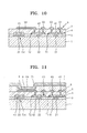
FIG. 10 is a schematic cross-sectional view of a patterned second insulating film formed on the second insulating film ofFIG. 9 ; and -
FIG. 11 is a schematic cross-sectional view of a third insulating film, an organic film, and a facing electrode, which are sequentially formed on the second insulating film ofFIG. 10 . - In the following detailed description, only certain exemplary embodiments of the present invention are shown and described, by way of illustration. As those skilled in the art would recognize, the invention may be embodied in many different forms and should not be construed as being limited to the embodiments set forth herein. Also, in the context of the present application, when an element is referred to as being "on" another element, it can be directly on the another element or be indirectly on the another element with one or more intervening elements interposed therebetween. Like reference numerals designate like elements throughout the specification.
-
FIGS. 1 through 11 are schematic cross-sectional views that illustrate methods of manufacturing an active matrix substrate and an organic light emitting display device, according to embodiments of the present invention. - Referring to
FIG. 1 , a firstconductive film 2 is formed on asubstrate 1. Thesubstrate 1 may be formed of a transparent glass material, and conventionally includes alkali-earth ions. A buffer layer that is formed mainly of SiO2 may further be formed on thesubstrate 1. - The first
conductive film 2 may be formed of a highly conductive metal used to form an electrode, for example, an alloy that includes Al, Ti, Mo, Ag, and/or Cr. - The first
conductive film 2 is patterned to a first pattern as shown inFIG. 2 by a photolithography process using a first photo mask. The photolithography process may be any suitable photolithography process. That is, after forming a first photoresist film on the firstconductive film 2, the first photoresist film is exposed through the first photo mask, and the firstconductive film 2 is patterned to the first pattern as shown inFIG. 2 through a development process and an etching process, and then, the first photoresist film remaining on the firstconductive film 2 is removed. - The first pattern includes a
first gate electrode 21, asecond gate electrode 22, and a capacitorlower electrode 23 as signal wires. - Next, referring to
FIG. 3 , a firstinsulating film 3, covering the first pattern that includes thefirst gate electrode 21, thesecond gate electrode 22, and the capacitorlower electrode 23, is formed on thesubstrate 1. The firstinsulating film 3 may be formed as an optically transparent insulating film, and may be formed of an oxide material that includes alkali ions and/or alkali-earth ions, for example, a silica group. - A semiconductor film is formed on the first
insulating film 3. - According to an embodiment of the present invention, the semiconductor film is formed using a semiconductor layer transfer printing method disclosed in U.S. Patent Publication No.
US2004/0229444 . - That is, referring to
FIG. 4 , after preparing asemiconductor wafer 45, a surface of thesemiconductor wafer 45 is implanted with ions. Thesemiconductor wafer 45 may be a mono-crystalline silicon wafer, but is not limited thereto, and may be a mono-crystalline wafer formed of a semiconductor material such as SiGe, SiC, Ge, GaAs, GaP, InP, or the like. - The ion implanting may be performed using hydrogen ions, but is not limited thereto, and may be performed using a mixture of boron ions and hydrogen ions or a mixture of helium ions and hydrogen ions.
- As a result of the ion implanting, a
semiconductor layer 4, which is a weakened region, is formed on a surface of thesemiconductor wafer 45. - The
semiconductor layer 4 formed in this way is oxidized after a washing process. The oxidization treatment may be an oxygen plasma treatment, a hydrogen peroxide treatment, a hydrogen peroxide and ammonia treatment, or a hydrogen peroxide and acid treatment. As a result of the oxidization treatment, hydroxyl groups are formed on the surface of thesemiconductor layer 4, and the surface of thesemiconductor layer 4 becomes hydrophilic. - Next, referring to
FIG. 5 , thesemiconductor wafer 45 is placed on the firstinsulating film 3 so that thesemiconductor layer 4 contacts the firstinsulating film 3 and is between thesemiconductor wafer 45 and the firstinsulating film 3. Here, according to one embodiment, the surface of the firstinsulating film 3 is washed and planarized before thesemiconductor wafer 45 is placed on the firstinsulating film 3. - Next, the
semiconductor layer 4 and the firstinsulating film 3 are attached to each other using an electrolysis method as described below in more detail. - First, both the
semiconductor layer 4 and the first insulatingfilm 3 are heated to different temperatures from each other before thesemiconductor layer 4 and the first insulatingfilm 3 are attached. The temperature difference is maintained to match the thermal expansion coefficients of thesemiconductor layer 4 and the first insulatingfilm 3, and thus, to separate (or peel off) thesemiconductor layer 4 from thesemiconductor wafer 45 in a subsequent process due to the thermal stress between thesemiconductor layer 4 and thesemiconductor wafer 45. In some embodiments, the temperature difference is between 100 to 150°C (or between about 100 and about 150°C). - Next, the
semiconductor layer 4 and the first insulatingfilm 3 are respectively maintained at uniform temperatures while compressing thesemiconductor layer 4 against the first insulatingfilm 3. Afterwards, a voltage is applied to thesemiconductor layer 4 and the first insulatingfilm 3, for example, using thesemiconductor layer 4 as an anode and the first insulatingfilm 3 as a cathode. - Due to the application of a voltage, alkali ions and/or alkali-earth ions present at an interface between the first insulating
film 3 and thesemiconductor layer 4 are moved to the first insulatingfilm 3. As a result, an alkali ion-free region and/or an alkali-earth ion-free region is present at the interface between the first insulatingfilm 3 and thesemiconductor layer 4, and thus, the first insulatingfilm 3 and thesemiconductor layer 4 are more strongly attached. - After the processes of compression and application of a voltage are maintained for a period of time (e.g., a predetermined period of time), the assembled structure is cooled at room temperature. Then, the
semiconductor wafer 45 separates from thesemiconductor layer 4 due to the thermal stress between thesemiconductor layer 4 and thesemiconductor wafer 45. - Referring to
FIG. 6 , thesemiconductor wafer 45 separates from thesemiconductor layer 4 using a peeling process. Here, thesemiconductor layer 4 remains attached to the first insulatingfilm 3. - After the
semiconductor layer 4 is formed as described above, thesemiconductor layer 4 may be maintained at a substantially uniform thickness through a surface washing process and an etching process. - The method of forming the
semiconductor layer 4 according to the present invention is not limited to the disclosed embodiments, and the semiconductor layer may be formed, for example, by depositing amorphous silicon on the first insulatingfilm 3. - Referring to
FIG. 7 , after coating asecond photoresist film 46 on thesemiconductor layer 4, thesecond photoresist film 46 is patterned into a second pattern. - Here, the patterning of the
second photoresist film 46 into the second pattern is performed using not an additional photo mask but the first pattern, that is, the pattern of thefirst gate electrode 21, thesecond gate electrode 22, and the capacitorlower electrode 23 by irradiating light toward the second resistfilm 46 from a lower side of thesubstrate 1. That is, when light is irradiated from the lower side of thesubstrate 1, regions of thesecond photoresist film 46 where the light is substantially blocked by the firstconductive film 2 of the first pattern, that is, by thefirst gate electrode 21, thesecond gate electrode 22, and the capacitorlower electrode 23, have a different degree of hardening from regions of thesecond photoresist film 46 where the light passes, and thus, the second pattern as shown inFIG. 7 is obtained when thesecond photoresist film 46 is etched. In the second pattern ofFIG. 7 , thesecond photoresist film 46 remains on thesemiconductor layer 4 in regions corresponding to upper parts of the firstconductive film 2 of the first pattern, that is, thefirst gate electrode 21, thesecond gate electrode 22, and the capacitorlower electrode 23, and the other regions of thesemiconductor layer 4 are exposed. - At this state, the exposed regions of the
semiconductor layer 4 are doped with p+ ions. The p+ ions may be any dopant that can form an active layer in a p-type metal-oxide semiconductor (PMOS) thin-film transistor, for example, B2H6 ions. - Next, referring to
FIG. 8 , after removing thesecond photoresist film 46, thesemiconductor layer 4 is patterned. Here, the photolithography process may be any suitable photolithography process. - That is, after removing the
second photoresist film 46, a third photoresist film is coated on thesemiconductor layer 4. Next, set or predetermined regions of thesemiconductor layer 4 are exposed by irradiating light thereon through a second photo mask and developing the third photoresist film. After etching the exposedsemiconductor layer 4, remaining portions of the third photoresist film are removed. Thus, thesemiconductor layer 4 having a third pattern as shown inFIG. 8 is obtained. - The third pattern includes a capacitor
upper electrode 43, a firstactive layer 41, and a secondactive layer 42. - The capacitor
upper electrode 43 is formed above the capacitorlower electrode 23, and is patterned to correspond to the capacitorlower electrode 23 to form a storage capacitor Cst. The firstactive layer 41 and the secondactive layer 42 are respectively active layer patterns in thin-film transistors. - Next, referring to
FIG. 9 , a secondinsulating film 5, covering the capacitorupper electrode 43, the firstactive layer 41, and the secondactive layer 42, is formed on the first insulatingfilm 3. - The second
insulating film 5 is patterned using a photolithography process to form contact holes through which source/drain regions of the firstactive layer 41 and the secondactive layer 42 are exposed. In this regard, the photolithography process may be any suitable photolithography process. - That is, after coating a fourth photoresist film on the second
insulating film 5, regions (e.g., predetermined regions) of the secondinsulating film 5 are exposed by irradiating light thereon through a third photo mask and developing the fourth photoresist film. After etching the exposed second insulatingfilm 5, remaining portions of the fourth photoresist film are removed. Thus, the secondinsulating film 5 having a fourth pattern as shown inFIG. 9 is obtained. - Next, after coating a second
conductive film 6 on the secondinsulating film 5, as shown inFIG. 10 , a fifth pattern is formed by patterning the secondconductive film 6. The fifth pattern of the secondconductive film 6 may be formed using any suitable photolithography process. - That is, first, after coating the second
conductive film 6 on the secondinsulating film 5, a fifth photoresist film is coated on the second conductive film. Regions (e.g., predetermined regions) of the secondconductive film 6 are exposed by irradiating light thereon through a fourth photo mask and developing the fifth photoresist film. After etching the secondconductive film 6, remaining portions of the fifth photoresist film are removed, and thus, the secondconductive film 6 as shown inFIG. 10 is obtained. - The fifth pattern of the second
conductive film 6 includes afirst source electrode 61 and afirst drain electrode 62, which are coupled (e.g., conductively coupled) to the firstactive layer 41, and asecond source electrode 63 and asecond drain electrode 64, which are coupled (e.g., conductively coupled) to the secondactive layer 42. According to another embodiment, the first andsecond source electrodes second drain electrodes - In the above structure, the
first gate electrode 21, the firstactive layer 41, thefirst source electrode 61, and thefirst drain electrode 62 constitute a first thin-film transistor T1, and thesecond gate electrode 22, the secondactive layer 42, thesecond source electrode 63, and thesecond drain electrode 64 constitute a second thin-film transistor T2. - In an exemplary embodiment, both the first and second thin-film transistors T1 and T2 are PMOS transistors.
- Also, the second thin-film transistor T2 is a pixel-driving thin-film transistor and the
second drain electrode 64 functions as a pixel electrode. Hereinafter, thereference numeral 64 is used to indicate both the second drain electrode and the pixel electrode. - As described above, the second
conductive film 6 that forms thefirst source electrode 61, thefirst drain electrode 62, thesecond source electrode 63, and thesecond drain electrode 64 may be formed of a suitable material used to form a pixel electrode. - When the
pixel electrode 64 is used as an anode electrode of an organic light emitting display device, thepixel electrode 64 may include a layer formed of a metal oxide having a high work function (absolute value), such as indium tin oxide (ITO), indium zinc oxide (IZO), and/or zinc oxide (ZnO). Also, in some embodiments, if the organic light emitting display device has a structure in which an image is projected in a direction toward an upper side of the organic light emitting display device, that is, in a direction opposite to (or facing oppositely away from) thesubstrate 1, the organic light emitting display device further includes a reflection film formed of an alloy of, for example, Al and Ag. Also, in some embodiments, thepixel electrode 64 is used as a cathode electrode of the organic light emitting display device, the pixel electrode 66 is formed of a highly conductive metal having a low work function (absolute value), such as Al, Ag, and/or Mg. In this case, the reflection film described above is unnecessary. - An active matrix substrate according to an exemplary embodiment of the present invention is formed using the process described above. As described above, in manufacturing the active matrix substrate, only four photo masks for patterning are used. Accordingly, the number of processes can be reduced, thereby increasing productivity, and thus, reducing manufacturing costs.
- Referring to
FIG. 11 , after manufacturing the active matrix substrate having a pattern of the secondconductive film 6, according to a further embodiment a thirdinsulating film 7 is formed on the secondconductive film 6 having the fifth pattern. The thirdconductive film 7 is patterned to form anopening 71 that exposes at least a portion of thepixel electrode 64 using any suitable photolithography process. - That is, after coating the third
insulating film 7 on the secondconductive film 6, a sixth photoresist film is coated on the thirdinsulating film 7. Next, a region (e.g., a predetermined region corresponding to the opening 71) of the thirdinsulating film 7 is exposed by irradiating light thereon through a fifth photo mask and developing the sixth photoresist film. After etching the exposed third insulatingfilm 7, the remaining sixth photoresist film is removed, and thus, the thirdinsulating film 7 having a sixth pattern as shown inFIG. 11 is obtained. - Next, an
organic film 8 is deposited on the thirdinsulating film 7. Theorganic film 8 may include a light emitting layer that can emit different colors in each pixel, and the light emitting layer is formed only on thepixel electrode 64 exposed through theopening 71. - In some embodiments, the
organic film 8 that includes the light emitting layer is formed of a material commonly used to form any suitable organic light emitting display devices, and includes at least one common layer selected from functional layers such as a hole transport layer (HTL), a hole injection layer (HIL), an electron transport layer (ETL), and/or an electron injection layer (EIL). Here, the at least one common layer refers to a layer that is formed over the entire pixels. - After forming the
organic film 8, a facingelectrode 9 is formed on theorganic film 8. During operation, a voltage having an opposite polarity to a voltage applied to thepixel electrode 64 is applied to the facingelectrode 9. That is, if thepixel electrode 64 is an anode electrode, the facingelectrode 9 is a cathode electrode, and vice versa. - If the organic light emitting display device is a top emission type in which an image emitted from the
organic film 8 is projected in a direction toward the facingelectrode 9, the facingelectrode 9 is formed to have high optical transmittance, and if the organic light emitting display device is a bottom emission type in which an image is projected in a direction toward thesubstrate 1, the facingelectrode 9 is formed to have high optical reflectance. - In manufacturing an organic light emitting display device according to an exemplary embodiment of the current invention, an active matrix substrate, which is a base substrate, is simply patterned using a reduced number of photo masks, thereby reducing manufacturing costs and increasing productivity.
- Also, a semiconductor layer of a thin-film transistor is formed of a mono-crystalline semiconductor material, and thus, a circuit having further improved characteristics can be realized.
- While the present invention has been described in connection with certain exemplary embodiments, it is to be understood that the invention is not limited to the disclosed embodiments, but, on the contrary, is intended to cover various modifications and equivalent arrangements included within the scope of the attached claims.
Claims (11)
- A method of manufacturing an active matrix substrate, the method comprising:forming a first electrode (21, 22, 23) having a first pattern on a substrate (1);forming a first insulating film (3) to cover the first electrode on the substrate;attaching a first layer (4) on a surface of a semiconductor wafer (45) to the first insulating film (3) by placing the semiconductor wafer on the first insulating film;transferring the first layer (4) onto the first insulating film to form a semiconductor layer on the first insulating film;doping a portion of the semiconductor layer with a dopant and patterning the semiconductor layer to form an active layer (41, 42);forming a second insulating film (5) to cover the active layer on the first insulating film; andforming a second electrode (61 - 64) coupled to the doped region of the active layer on the second insulating film.
- The method of claim 1, wherein the attaching of the first layer on the surface of the semiconductor wafer to the first insulating film comprises:forming the first layer (4) on the surface of the semiconductor wafer (45);heating the semiconductor wafer with a first temperature and the first insulating film (3) with a second temperature different from the first temperature;bringing the first layer on the surface of the semiconductor wafer into contact with the first insulating film (3);applying a voltage between the semiconductor wafer and the first insulating film; andpeeling a portion of the semiconductor wafer from the first insulating film such that the first layer (4) remains attached to the first insulating film (3).
- The method of claim 2, wherein the forming of the first layer on the surface of the semiconductor wafer comprises ion implanting a gas comprising hydrogen ions into a surface of the semiconductor wafer.
- The method of any one of claims 1, 2 or 3, wherein the semiconductor wafer comprises mono-crystalline silicon.
- The method of any one of the preceding claims, wherein the doping of the portion of the semiconductor layer with the dopant and patterning of the semiconductor layer to form the active layer comprises:forming a first resist layer (46) on the semiconductor layer to cover a first portion of the semiconductor layer and to expose a first region of the semiconductor layer through an opening in the first resist layer;doping the first region of the semiconductor layer with a dopant through the opening in the first resist layer;removing the first resist layer; andpatterning the semiconductor layer into a second pattern to form the active layer.
- The method of claim 5, wherein a pattern of the opening in the first resist layer is substantially identical to a pattern in which portions other than portions of the first resist layer corresponding to the first pattern of the first electrode are etched.
- The method of claim 5 or 6, wherein the forming of the first resist layer comprises:exposing the first resist layer (46) to light from a lower side of the substrate in accordance with the pattern of the first electrode (21, 22, 23); andetching the first resist layer so as to maintain portions of the first resist layer substantially corresponding in position to the first pattern of the first electrode.
- The method of any one of claims 5 to 7, wherein the patterning of the semiconductor layer into the second pattern is performed prior to the forming of the first resist layer.
- A method of manufacturing an organic light emitting display device, comprising carrying out a method according to any one of the preceding claims, wherein:the step of forming the first electrode comprises forming a first gate electrode (21) and a second gate electrode (22) on the substrate (1);the step of forming the first insulating film (3) comprises forming the first insulating film to cover the first and second gate electrodes;the step of doping a portion of the semiconductor layer with a dopant and patterning the seminconductor layer to form an active layer comprises doping first and second regions of the semiconductor layer and patterning the semiconductor layer to form a first active layer (41) having a first region and a second active layer (42) having a second region, wherein the first region and the second region are doped with the same type of dopant;the step of forming the second insulating film (5) comprises forming the second insulating film to cover the first and second active layers on the first insulating film; andthe step of forming a second electrode comprises forming the second electrode coupled to the first region and the second region.
- The method of claim 9, further comprising forming holes in the second insulating film to expose the first and second regions of the semiconductor layer prior to forming the second electrode, the method further comprising:forming a pixel electrode (64) coupled to the second region on the second insulating film; andforming a third insulating film (7) to cover the second electrode and the pixel electrode on the second insulating film;forming an opening in the third insulating film to expose at least one portion of the pixel electrode;forming an organic film (8) comprising a light emitting layer on the at least one portion of the pixel electrode exposed through the opening in the third insulating film; andforming a facing electrode (9) to cover the organic film.
- The method of claim 9 or 10, wherein the forming of the first resist layer comprises:exposing the first resist layer to light from a lower side of the substrate in accordance with a pattern of the first gate electrode and the second gate electrode; andetching the first resist layer so as to maintain portions of the first resist layer to substantially correspond in position to the pattern of first gate electrode and the second gate electrode.
Applications Claiming Priority (1)
| Application Number | Priority Date | Filing Date | Title |
|---|---|---|---|
| KR1020090029560A KR101127574B1 (en) | 2009-04-06 | 2009-04-06 | Manufacturing methods of active matrix substrate and organic light emitting display device |
Publications (1)
| Publication Number | Publication Date |
|---|---|
| EP2239780A1 true EP2239780A1 (en) | 2010-10-13 |
Family
ID=42235328
Family Applications (1)
| Application Number | Title | Priority Date | Filing Date |
|---|---|---|---|
| EP10155496A Withdrawn EP2239780A1 (en) | 2009-04-06 | 2010-03-04 | Methods of manufacturing active matrix substrate and organic light-emitting display device |
Country Status (5)
| Country | Link |
|---|---|
| US (1) | US7989240B2 (en) |
| EP (1) | EP2239780A1 (en) |
| JP (1) | JP5227995B2 (en) |
| KR (1) | KR101127574B1 (en) |
| CN (1) | CN101859732B (en) |
Cited By (1)
| Publication number | Priority date | Publication date | Assignee | Title |
|---|---|---|---|---|
| JP2012195283A (en) * | 2011-03-14 | 2012-10-11 | Samsung Mobile Display Co Ltd | Organic light-emitting display device and method of manufacturing the same |
Families Citing this family (2)
| Publication number | Priority date | Publication date | Assignee | Title |
|---|---|---|---|---|
| KR101094296B1 (en) * | 2010-05-31 | 2011-12-19 | 삼성모바일디스플레이주식회사 | Display device and Fabrication method of the same |
| KR101705822B1 (en) * | 2010-10-27 | 2017-02-23 | 삼성디스플레이 주식회사 | Organic light emitting display apparatus and method of manufacturing thereof |
Citations (4)
| Publication number | Priority date | Publication date | Assignee | Title |
|---|---|---|---|---|
| EP1168435A2 (en) * | 2000-06-28 | 2002-01-02 | Sel Semiconductor Energy Laboratory Co., Ltd. | Semiconductor device and manufacturing method thereof |
| WO2003103041A2 (en) * | 2002-06-04 | 2003-12-11 | Philips Intellectual Property & Standards Gmbh | Semiconductor device and method of manufacturing same |
| US20040229444A1 (en) | 2003-02-18 | 2004-11-18 | Couillard James G. | Glass-based SOI structures |
| US20090078939A1 (en) * | 2007-09-20 | 2009-03-26 | Semiconductor Energy Laboratory Co., Ltd. | Display device and method for manufacturing the same |
Family Cites Families (14)
| Publication number | Priority date | Publication date | Assignee | Title |
|---|---|---|---|---|
| GB9929615D0 (en) * | 1999-12-15 | 2000-02-09 | Koninkl Philips Electronics Nv | Method of manufacturing an active matrix device |
| JP4678933B2 (en) * | 2000-11-07 | 2011-04-27 | 株式会社半導体エネルギー研究所 | Method for manufacturing semiconductor device |
| US7399681B2 (en) * | 2003-02-18 | 2008-07-15 | Corning Incorporated | Glass-based SOI structures |
| KR20050113045A (en) * | 2004-05-28 | 2005-12-01 | 삼성에스디아이 주식회사 | Organic light emitting display device and the method for fabricating of the same |
| KR100611886B1 (en) | 2004-06-25 | 2006-08-11 | 삼성에스디아이 주식회사 | Pixel circuit and organic light emitting display having an improved transistor structure |
| US7410883B2 (en) * | 2005-04-13 | 2008-08-12 | Corning Incorporated | Glass-based semiconductor on insulator structures and methods of making same |
| US7268051B2 (en) * | 2005-08-26 | 2007-09-11 | Corning Incorporated | Semiconductor on glass insulator with deposited barrier layer |
| JP2007103584A (en) * | 2005-10-03 | 2007-04-19 | Ricoh Co Ltd | Transistor element, display device and manufacturing methods thereof |
| US7691730B2 (en) | 2005-11-22 | 2010-04-06 | Corning Incorporated | Large area semiconductor on glass insulator |
| US7456080B2 (en) | 2005-12-19 | 2008-11-25 | Corning Incorporated | Semiconductor on glass insulator made using improved ion implantation process |
| US7790565B2 (en) * | 2006-04-21 | 2010-09-07 | Corning Incorporated | Semiconductor on glass insulator made using improved thinning process |
| US20070277874A1 (en) * | 2006-05-31 | 2007-12-06 | David Francis Dawson-Elli | Thin film photovoltaic structure |
| JP5325404B2 (en) * | 2007-09-21 | 2013-10-23 | 株式会社半導体エネルギー研究所 | Method for manufacturing SOI substrate |
| WO2009145882A1 (en) * | 2008-05-30 | 2009-12-03 | Corning Incorporated | Thin film transistor having a common channel and selectable doping configuration |
-
2009
- 2009-04-06 KR KR1020090029560A patent/KR101127574B1/en active IP Right Grant
-
2010
- 2010-01-08 CN CN201010001459.5A patent/CN101859732B/en active Active
- 2010-01-28 US US12/695,933 patent/US7989240B2/en active Active
- 2010-03-04 EP EP10155496A patent/EP2239780A1/en not_active Withdrawn
- 2010-04-02 JP JP2010086143A patent/JP5227995B2/en active Active
Patent Citations (4)
| Publication number | Priority date | Publication date | Assignee | Title |
|---|---|---|---|---|
| EP1168435A2 (en) * | 2000-06-28 | 2002-01-02 | Sel Semiconductor Energy Laboratory Co., Ltd. | Semiconductor device and manufacturing method thereof |
| WO2003103041A2 (en) * | 2002-06-04 | 2003-12-11 | Philips Intellectual Property & Standards Gmbh | Semiconductor device and method of manufacturing same |
| US20040229444A1 (en) | 2003-02-18 | 2004-11-18 | Couillard James G. | Glass-based SOI structures |
| US20090078939A1 (en) * | 2007-09-20 | 2009-03-26 | Semiconductor Energy Laboratory Co., Ltd. | Display device and method for manufacturing the same |
Cited By (3)
| Publication number | Priority date | Publication date | Assignee | Title |
|---|---|---|---|---|
| JP2012195283A (en) * | 2011-03-14 | 2012-10-11 | Samsung Mobile Display Co Ltd | Organic light-emitting display device and method of manufacturing the same |
| EP2500946A3 (en) * | 2011-03-14 | 2014-03-05 | Samsung Display Co., Ltd. | Organic light-emitting display and method of manufacturing the same |
| US8901563B2 (en) | 2011-03-14 | 2014-12-02 | Samsung Display Co., Ltd. | Organic light-emitting display device and method of manufacturing the same |
Also Published As
| Publication number | Publication date |
|---|---|
| CN101859732B (en) | 2014-08-06 |
| JP5227995B2 (en) | 2013-07-03 |
| KR20100111145A (en) | 2010-10-14 |
| US20100255617A1 (en) | 2010-10-07 |
| US7989240B2 (en) | 2011-08-02 |
| JP2010245537A (en) | 2010-10-28 |
| CN101859732A (en) | 2010-10-13 |
| KR101127574B1 (en) | 2012-03-23 |
Similar Documents
| Publication | Publication Date | Title |
|---|---|---|
| US8569122B2 (en) | Manufacturing method for LTPS TFT array substrate | |
| US8278664B2 (en) | Organic light emitting display device and method of fabricating the same | |
| US6617203B2 (en) | Flat panel display device and method of manufacturing the same | |
| TWI529810B (en) | Methods of fabricating metal oxide or metal oxynitride tfts using wet process for source-drain metal etch | |
| KR101280827B1 (en) | Array substrate and method of fabricating the same | |
| KR100579182B1 (en) | Methode of fabricating OELDOrganic Electro Luminescence Display | |
| WO2016112663A1 (en) | Array substrate manufacturing method and array substrate | |
| EP2216821A2 (en) | Organic light emitting diode display and method of manufacturing the same | |
| US9793413B2 (en) | Metal oxide thin film transistor having channel protection layer | |
| US20050110021A1 (en) | Active matrix organic light emitting display (OLED) and method of fabrication | |
| US9735186B2 (en) | Manufacturing method and structure thereof of TFT backplane | |
| WO2016141805A1 (en) | Preparation methods for thin-film layer pattern, thin-film transistor and array substrate | |
| US9647014B2 (en) | Complementary thin film transistor driving back plate and preparing method thereof, and display device | |
| TWI419336B (en) | Semiconductor device and method of making the same | |
| WO2016026176A1 (en) | Method for manufacturing tft substrate, and structure of tft substrate | |
| US7989240B2 (en) | Methods of manufacturing active matrix substrate and organic light-emitting display device | |
| US7985608B2 (en) | Methods of manufacturing active matrix substrate and organic light emitting display device | |
| US20090258169A1 (en) | Method for manufacturing a patterned metal layer | |
| KR101920225B1 (en) | organic electro luminescent device and method of fabricating array substrate for the same | |
| KR100684175B1 (en) | Method for manufacturing electroluminescence devices | |
| KR20120062193A (en) | Manufacturing method of flexible display device | |
| KR101599280B1 (en) | Method of fabricating an array substrate | |
| KR101475411B1 (en) | Poly-Si thin film transistor and method of manufacturing the same | |
| TWI466298B (en) | Method for manufacturing pixel structure | |
| WO2020246694A1 (en) | Method for manufacturing display device |
Legal Events
| Date | Code | Title | Description |
|---|---|---|---|
| PUAI | Public reference made under article 153(3) epc to a published international application that has entered the european phase |
Free format text: ORIGINAL CODE: 0009012 |
|
| 17P | Request for examination filed |
Effective date: 20100304 |
|
| AK | Designated contracting states |
Kind code of ref document: A1 Designated state(s): AT BE BG CH CY CZ DE DK EE ES FI FR GB GR HR HU IE IS IT LI LT LU LV MC MK MT NL NO PL PT RO SE SI SK SM TR |
|
| AX | Request for extension of the european patent |
Extension state: AL BA ME RS |
|
| RAP1 | Party data changed (applicant data changed or rights of an application transferred) |
Owner name: SAMSUNG DISPLAY CO., LTD. |
|
| RAP1 | Party data changed (applicant data changed or rights of an application transferred) |
Owner name: SAMSUNG DISPLAY CO., LTD. |
|
| STAA | Information on the status of an ep patent application or granted ep patent |
Free format text: STATUS: THE APPLICATION HAS BEEN WITHDRAWN |
|
| 18W | Application withdrawn |
Effective date: 20161004 |