EP2323008A2 - Electronic device with reduced power consumption in external memory - Google Patents
Electronic device with reduced power consumption in external memory Download PDFInfo
- Publication number
- EP2323008A2 EP2323008A2 EP10190744A EP10190744A EP2323008A2 EP 2323008 A2 EP2323008 A2 EP 2323008A2 EP 10190744 A EP10190744 A EP 10190744A EP 10190744 A EP10190744 A EP 10190744A EP 2323008 A2 EP2323008 A2 EP 2323008A2
- Authority
- EP
- European Patent Office
- Prior art keywords
- clock
- external memory
- clock signal
- memory
- electronic device
- Prior art date
- Legal status (The legal status is an assumption and is not a legal conclusion. Google has not performed a legal analysis and makes no representation as to the accuracy of the status listed.)
- Granted
Links
- 230000015654 memory Effects 0.000 title claims abstract description 124
- 238000012545 processing Methods 0.000 claims abstract description 10
- 230000003068 static effect Effects 0.000 description 10
- 101150102323 PDYN gene Proteins 0.000 description 6
- 230000007423 decrease Effects 0.000 description 4
- 238000004891 communication Methods 0.000 description 2
- 230000001419 dependent effect Effects 0.000 description 2
- 230000006870 function Effects 0.000 description 2
- 238000012546 transfer Methods 0.000 description 2
- 239000003990 capacitor Substances 0.000 description 1
- 230000003247 decreasing effect Effects 0.000 description 1
- 230000010365 information processing Effects 0.000 description 1
- 238000012886 linear function Methods 0.000 description 1
- 238000000034 method Methods 0.000 description 1
- 238000012986 modification Methods 0.000 description 1
- 230000004048 modification Effects 0.000 description 1
- 230000009467 reduction Effects 0.000 description 1
- 230000004044 response Effects 0.000 description 1
Images

Classifications
-
- G—PHYSICS
- G06—COMPUTING; CALCULATING OR COUNTING
- G06F—ELECTRIC DIGITAL DATA PROCESSING
- G06F13/00—Interconnection of, or transfer of information or other signals between, memories, input/output devices or central processing units
- G06F13/38—Information transfer, e.g. on bus
- G06F13/42—Bus transfer protocol, e.g. handshake; Synchronisation
- G06F13/4204—Bus transfer protocol, e.g. handshake; Synchronisation on a parallel bus
- G06F13/4234—Bus transfer protocol, e.g. handshake; Synchronisation on a parallel bus being a memory bus
- G06F13/4243—Bus transfer protocol, e.g. handshake; Synchronisation on a parallel bus being a memory bus with synchronous protocol
-
- G—PHYSICS
- G06—COMPUTING; CALCULATING OR COUNTING
- G06F—ELECTRIC DIGITAL DATA PROCESSING
- G06F1/00—Details not covered by groups G06F3/00 - G06F13/00 and G06F21/00
- G06F1/26—Power supply means, e.g. regulation thereof
- G06F1/32—Means for saving power
- G06F1/3203—Power management, i.e. event-based initiation of a power-saving mode
- G06F1/3234—Power saving characterised by the action undertaken
- G06F1/325—Power saving in peripheral device
- G06F1/3275—Power saving in memory, e.g. RAM, cache
-
- Y—GENERAL TAGGING OF NEW TECHNOLOGICAL DEVELOPMENTS; GENERAL TAGGING OF CROSS-SECTIONAL TECHNOLOGIES SPANNING OVER SEVERAL SECTIONS OF THE IPC; TECHNICAL SUBJECTS COVERED BY FORMER USPC CROSS-REFERENCE ART COLLECTIONS [XRACs] AND DIGESTS
- Y02—TECHNOLOGIES OR APPLICATIONS FOR MITIGATION OR ADAPTATION AGAINST CLIMATE CHANGE
- Y02D—CLIMATE CHANGE MITIGATION TECHNOLOGIES IN INFORMATION AND COMMUNICATION TECHNOLOGIES [ICT], I.E. INFORMATION AND COMMUNICATION TECHNOLOGIES AIMING AT THE REDUCTION OF THEIR OWN ENERGY USE
- Y02D10/00—Energy efficient computing, e.g. low power processors, power management or thermal management
Definitions
- a typical, prior art version of such an electrical device contains a Central Processing Unit (CPU) 3 for processing and controlling the whole electrical device, a Closely Coupled Memory (CCM) 5 for storing data and/or instructions, an external memory system 8 comprising external memory as well as a related external memory bus controller 13 and which external memory 8 is arranged for storing data and/or instructions.
- a clock unit 1 receives a master clock signal 2 for generating a main system clock signal 6 for the electrical device, i.e. for the CPU 3, the CCM 5 and the external memory 8.
- the device comprises an internal memory bus 4 for connecting the CPU 3 with the CCM 5, and an external memory bus 7 for connecting the CCM 5 with the external memory 8.
- the memory bus controller 13 is integrated on the chip and is connected to the CPU 3 to receive read and write instructions from CPU 3. After having received a read request from CPU 3, memory bus controller 13 retrieves the requested data from external memory 7 for CCM 5.
- CCM 5 is arranged to receive that data and to store it at a predetermined memory location where CPU 3 can access it.
- the CPU 3, the clock unit 1, the CCM 5 and the memory bus controller 13 are integrated in one single chip 14 (embedded).
- the CCM 5 is the smallest and fastest type of memory.
- the CCM 5 is optimized for speed rather than size.
- the external memory 8 is connected to the CCM 5 through external memory bus 7.
- the external memory 8 can be cost optimized for size and is usually slower than the integrated CCM 5.
- the electrical device is clocked by master clock signal 2.
- the clock unit 1 converts the master clock signal 2 into a faster version of the master clock signal 2 (e.g. by a Phase Locked Loop) or a slower version of master clock signal 2 (e.g. by a Clock Divider).
- the input of clock unit 1 is the master clock signal 2 and the output of clock unit 1 is the main system clock signal 6.
- the main system clock signal 6 clocks the CPU 3, CCM 5, external memory controller 13 and external memory 8.
- the power Pccm active consumed by the CPU 3, CCM 5 and other components on the chip which are active when the device is active consists of two components. One being a static power consumption Pccm static and the second one being a dynamic power consumption Pccm dynamic , which is dependent on the speed on which the device is operated.
- Pccm active Pccm static + Pccm ⁇ f clock dynamic
- Pccm(f clock ) dynamic is a function of f clock :
- Pccm ( f clock ⁇ ) dynamic f clock * A Pdyn CCM
- the main system clock signal 6 is designed to be equal to or slower than the master clock signal 2 for the sake of conserving power.
- the dynamic power consumption of components which are active when the device is active such as CPU 3 and CCM 5 will be lower than the situation when the main system clock signal 6 is the same as the master clock signal 2.
- the processor 3 will fetch a high percentage of its instructions from CCM 5 over internal memory bus 4 (in the order of 90% or higher) and only few instructions need to be fetched from the external memory 8 over external memory bus 7.
- the average bus speed will be close to the speed of internal memory bus 4 as most instructions are fetched from the fast CCM 5. Fetching the remaining instructions from the external memory 8 is relatively slow, but since the number of instructions is limited this has a minor impact on the average bus speed.
- the power Pext active consumed by the external memory 8 while active consists of two components.
- the second one being the dynamic power consumption Pext dynamic , which is dependent on the speed, i.e. the clock frequency, the device is operated.
- Pext active Pext static + Pext ⁇ f clock dynamic
- Pext(f clock ) dynamic is a function of f clock :
- Pext ( f clock ⁇ ) dynamic f clock * A Pdyn ext
- the total power consumption consumed by the external memory 8 while inactive consists of one component; i.e. the standby power consumption Pext standby . It is commonly known that the standby power consumption Pext standby is smaller than the static power consumption Pext static .
- T active C 0 * N / f clock
- C 0 constant [HZ]
- N bytes can consist of either the following items or a combination of the following items:
- the access format to the external memory is not limited to the above items.
- the object of the invention is to reduce the overall system power consumption while still operating the device at a suitable, acceptable speed.
- the invention is based on the insight that the lowest current consumption of the device comprising internal components and an external memory can be achieved by clocking the internal components at the lowest clock speed possible to preform the necessary actions on the CPU and the external memory at the highest speed possible.
- the internal components including the CPU are running at a low clock, the average amount of data per time unit to be retrieved from the external memory will be much lower than the maximum amount of data per time unit that can be retrieved from the external memory.
- One skilled in the art could decide to clock the external memory with a low clock which is suitable to retrieve the average amount of data per time unit from the external memory.
- the average amount of data per time unit could be retrieved from the external memory in a short time in said time unit. This allows the device to switch the external memory from active state to standby state, which consequently results in a reduction of the overall system power consumption as explained above.
- EP1653331A2 discloses a system with a memory clock and a processor clock. In a sleep state which corresponds to a low power mode, the processor clock and memory clock are power down. Said document does not disclose the relationship between the processor clock and memory clock when the processor is running at a relative low frequency with respect to its normal frequency.
- US2008/0005607 discloses a method of controlling an information processing device. A controlling unit decreases the frequencies of the CPU when a cache hit rate is low, and increases the frequencies of the CPU when the cache hit rate is high. Furthermore, the controlling unit increases the frequencies of the Memory clock when a cache hit rate is low, and decreases the frequencies of the CPU when the cache hit rate is high.
- US2007//0183192 discloses a system wherein a memory is driven by a constant memory clock and a processor is driven by a variable processor clock.
- US6384651B1 discloses a system with a processor and memory clock which are switched on and off with a predefined duty cycle.
- the processor clock is in the hundreds of MHz and the MCLK is at 100 MHz.
- the device according to figure 2 comprises a separate clock unit 9 for generating a separate external clock signal 10 with an external clock frequency f clock,10 to the external memory 8.
- the clock unit 9 receives clock signal 2 as input signal and derives external clock signal 10 from that clock signal 2.
- the frequency f clock,10 of clock signal 10 can be controlled separately from the clock frequency f clock of the clock signal 6.
- the frequency f clock,10 of clock signal 10 can be made higher than the clock frequency f clock of the clock signal 6.
- the external clock frequency f clock,10 should be made as high as possible and consequently providing the possibility to increase the relative standby period T standby of the external memory 8 and decreasing the relative active period T active of the external memory 8 within a time unit while still receiving a predetermined amount of data per time unit from the external memory.
- the clock unit 9 is arranged to produce external clock signal 10 with an external clock frequency f clock,10 as close as possible to the clock frequency of clock signal 2.
- the clock unit 9 may, again be based on an implementation with a phase locked loop or a frequency divider. However, the invention is not restricted to such an embodiment.
- the bus controller 13 receives the clock signal 10 as an input signal and is arranged to operate the transfer of data from external memory 8 to CCM 5 via external memory bus 7 at a maximum possible frequency.
- FIG. 2 shows that both clock unit 1 and clock unit 9 receive clock signal 2 and produce their output clock signals based on this input signal.
- clock unit 1 may be coupled to the output of clock unit 9 such as to receive clock signal 10 as an input and derive its output clock signal from clock signal 10.
- clock signals 6 and 10 are not independently controlled.
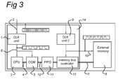
- FIG. 3 shows an alternative embodiment of the invention.
- the same reference signs are used for the same components as in the preceding figures.
- the embodiment of figure 3 comprises a FIFO (First In First Out) buffer 11 between external memory bus 7 and CCM 5.
- the FIFO 11 is connected to external memory bus 7 and to a system bus 12 that is, at its other end, also connected to CCM 5.
- Bus controller 13 is connected to FIFO 11 too.
- the system of figure 3 provides more flexibility because the FIFO arranges for synchronization of the speed of transfer of data at the output of external memory 8 to the speed of receipt of data at the input of CCM 5. By doing so, bus throughput differences between system bus 12 at the input of CCM 5 and external memory bus 12 at the output of external memory 8 are equalized.
- the way how such a FIFO operates is known to persons skilled in the art and does not need any further explanation here.
- the first clock unit 1 generates a first clock signal 6 having a first clock frequency.
- a second clock unit 9 generates a second clock signal 10 having a second clock frequency.
- the second clock frequency is higher than the first clock frequency.
- the clock frequency of the first clock signal could be in the order of 100kHz and the clock frequency of the second clock signal could be in the order of 10MHz.
- the device is configured to switch per time unit the external memory for an active period T active in an active state and for a standby period T standby in a standby state.
- the first clock frequency of the first clock signal 6 is preferably as low as possible to allow the processor CPU 3 to perform the necessary actions defined by the instructions available in the closely coupled memory CCM 5.
- CCM 5 is for example a cache memory.
- the hit rate of instructions available in the CCM 5 will determine the amount of data per time unit that has to be retrieve from the external memory.
- the amount of data per time unit that has to be retrieved from the memory will decrease linearly with the decrease of the first clock frequency.
- the external memory 8 could be switched between standby mode and active mode under control of a chip_select signal or chip_enable signal, which signals are known the person skilled in the art to control a memory device.
- the device is configured to disable the second clock signal when the memory is switched in the standby state. Disabling the second clock signal at the output of the second clock unit 9, reduces further the power consumption.
- the wires and bond paths from the output of the second clock unit 9 to the external memory 8 and memory bus controller are small capacitors which dissipate power when a clock signal is supplied to them.
- the memory controller 13 will disable the second clock signal 10 or second clock unit 9. Circuitry running on the first clock signal 6 will enable the second clock signal 10 or second clock unit 9 to supply a clock signal with the second clock frequency to the external memory 8 and memory bus controller 13.
- a data element could be a specified number of bytes forming an instruction, a parameter or other data.
- the retrieval of the amount of data corresponding to one instruction is sufficient and the communication could be stopped after receipt of said amount of data even if the external memory would like to transmit further data elements in response to the received command.
- the communication between the memory bus controller and the external memory 8 could be stopped by deselecting the external memory by means of a chip-select signal or chip-enable signal.
Abstract
Description
- Many electronic devices have an embedded processor with several types of memory connected through a bus. Usually there are several stages of memory connected to the processor, varying in size and speed.
- As is shown in
figure 1 , a typical, prior art version of such an electrical device contains a Central Processing Unit (CPU) 3 for processing and controlling the whole electrical device, a Closely Coupled Memory (CCM) 5 for storing data and/or instructions, anexternal memory system 8 comprising external memory as well as a related externalmemory bus controller 13 and whichexternal memory 8 is arranged for storing data and/or instructions. Aclock unit 1 receives amaster clock signal 2 for generating a mainsystem clock signal 6 for the electrical device, i.e. for theCPU 3, theCCM 5 and theexternal memory 8. The device comprises aninternal memory bus 4 for connecting theCPU 3 with theCCM 5, and anexternal memory bus 7 for connecting theCCM 5 with theexternal memory 8. - The
memory bus controller 13 is integrated on the chip and is connected to theCPU 3 to receive read and write instructions fromCPU 3. After having received a read request fromCPU 3,memory bus controller 13 retrieves the requested data fromexternal memory 7 forCCM 5. CCM 5 is arranged to receive that data and to store it at a predetermined memory location whereCPU 3 can access it. - The
CPU 3, theclock unit 1, theCCM 5 and thememory bus controller 13 are integrated in one single chip 14 (embedded). The CCM 5 is the smallest and fastest type of memory. The CCM 5 is optimized for speed rather than size. As the CCM 5 is integrated into the device, the cost per byte is relatively high. Theexternal memory 8 is connected to the CCM 5 throughexternal memory bus 7. Theexternal memory 8 can be cost optimized for size and is usually slower than the integratedCCM 5. The electrical device is clocked bymaster clock signal 2. Theclock unit 1 converts themaster clock signal 2 into a faster version of the master clock signal 2 (e.g. by a Phase Locked Loop) or a slower version of master clock signal 2 (e.g. by a Clock Divider). The input ofclock unit 1 is themaster clock signal 2 and the output ofclock unit 1 is the mainsystem clock signal 6. The mainsystem clock signal 6 clocks theCPU 3,CCM 5,external memory controller 13 andexternal memory 8. - The power Pccmactive consumed by the
CPU 3,CCM 5 and other components on the chip which are active when the device is active consists of two components. One being a static power consumption Pccmstatic and the second one being a dynamic power consumption Pccmdynamic, which is dependent on the speed on which the device is operated. The following formula holds:
- In this formula,
Pccm(fclock)dynamic is a function of fclock:
Where: - APdyn(CCM) is a constant with unit [W/Hz],
- fclock = frequency of main
system clock signal 6 in Hz as received byCCM 5. - From the formula it is clear that minimum power consumption for components in the system which are active when the device is active is achieved when fclock is as low as possible. Therefore, the main
system clock signal 6 is designed to be equal to or slower than themaster clock signal 2 for the sake of conserving power. By making the mainsystem clock signal 6 slower than themaster clock signal 2, the dynamic power consumption of components which are active when the device is active, such asCPU 3 andCCM 5, will be lower than the situation when the mainsystem clock signal 6 is the same as themaster clock signal 2. When the CCM 5 is used as a cache memory, theprocessor 3 will fetch a high percentage of its instructions fromCCM 5 over internal memory bus 4 (in the order of 90% or higher) and only few instructions need to be fetched from theexternal memory 8 overexternal memory bus 7. In this way, the average bus speed will be close to the speed ofinternal memory bus 4 as most instructions are fetched from the fast CCM 5. Fetching the remaining instructions from theexternal memory 8 is relatively slow, but since the number of instructions is limited this has a minor impact on the average bus speed. - The power Pextactive consumed by the
external memory 8 while active consists of two components. One being the static power consumption Pextstatic which is always present when the device is active, for example when the device is selected by means of a chip_select signal or chip_enable signal. The second one being the dynamic power consumption Pextdynamic, which is dependent on the speed, i.e. the clock frequency, the device is operated.
- In this formula,
Pext(fclock)dynamic is a function of fclock:
Where: - APdyn(ext) is a constant with unit [W/Hz],
- fclock = frequency of main
system clock signal 6 in Hz as received byexternal memory 8 - The total power consumption consumed by the
external memory 8 while inactive consists of one component; i.e. the standby power consumption Pextstandby. It is commonly known that the standby power consumption Pextstandby is smaller than the static power consumption Pextstatic. - The total power Pexttotal consumed by the
external memory device 8 is equal to the active power consumption Pextactive multiplied by the relative active period Tactive (defined as part per unit time) plus the standby power consumption Pextstandby multiplied by the relative standby period Tstandby(defined as part per unit time). So, Tactive + Tstandby = 1, and:

- Assume the amount of data per time unit retrieved is a linear function of the frequency fclock of the main
system clock signal 6 as received byexternal memory 8, then the relative active period Tactive can be expressed as follows when retrieving N bytes.
Where C0 = constant [HZ] - When accessing the
external memory 8 we may assume these N bytes can consist of either the following items or a combination of the following items: - A command (write / read / status / ...)
- An address (which byte or data the command has to operate on)
- Data (actual payload)
- The access format to the external memory is not limited to the above items.
- This means:

- Given that Pextstatic, APdyn(ext) and P(ext)standby are constants, the formula can be written as:

Where: - C1= Pextstatic - Pextstandby
- C2 = APdyn(ext)
- C3 = Pextstandby
- From the formula it is clear that minimum power consumption is achieved when fclock is as high as possible, for any given amount of data N per time unit. However, this is in direct conflict with formula (1) which states the minimum power consumption of components in the system which are active when the system is active can be achieved by using a low fclock.
- The object of the invention is to reduce the overall system power consumption while still operating the device at a suitable, acceptable speed.
- This object is obtained by a device as claimed in
claim 1. - The invention is based on the insight that the lowest current consumption of the device comprising internal components and an external memory can be achieved by clocking the internal components at the lowest clock speed possible to preform the necessary actions on the CPU and the external memory at the highest speed possible. When the internal components including the CPU are running at a low clock, the average amount of data per time unit to be retrieved from the external memory will be much lower than the maximum amount of data per time unit that can be retrieved from the external memory. One skilled in the art could decide to clock the external memory with a low clock which is suitable to retrieve the average amount of data per time unit from the external memory. However, by using a clock for the external memory with a clock frequency which is higher than the clock frequency of the internal components, more particularly the CPU, the average amount of data per time unit could be retrieved from the external memory in a short time in said time unit. This allows the device to switch the external memory from active state to standby state, which consequently results in a reduction of the overall system power consumption as explained above.
- It should be noted that
EP1653331A2 discloses a system with a memory clock and a processor clock. In a sleep state which corresponds to a low power mode, the processor clock and memory clock are power down. Said document does not disclose the relationship between the processor clock and memory clock when the processor is running at a relative low frequency with respect to its normal frequency.US2008/0005607 discloses a method of controlling an information processing device. A controlling unit decreases the frequencies of the CPU when a cache hit rate is low, and increases the frequencies of the CPU when the cache hit rate is high. Furthermore, the controlling unit increases the frequencies of the Memory clock when a cache hit rate is low, and decreases the frequencies of the CPU when the cache hit rate is high. It does not disclose that the memory is switched between an active state and standby state to reduce power when the processor is running at a particular frequency.US2007//0183192 discloses a system wherein a memory is driven by a constant memory clock and a processor is driven by a variable processor clock. -
US6384651B1 discloses a system with a processor and memory clock which are switched on and off with a predefined duty cycle. The processor clock is in the hundreds of MHz and the MCLK is at 100 MHz. - The invention will be explained in detail with reference to some drawings that are only intended to show embodiments of the invention and not to limit the scope. The scope of the invention is defined in the annexed claims and by its technical equivalents.
- The drawings show:
-
Figure 1 is a simplified, prior art schematic view of an electronic device with a CPU, a clock unit and some memories. -
Figure 2 is an example of an electronic device with a separate clock unit for the external memory according to the invention. -
Figure 3 shows an alternative embodiment of the invention. - In
figure 2 , reference numbers which are the same as infigure 1 refer to the same components. - The device according to
figure 2 comprises aseparate clock unit 9 for generating a separateexternal clock signal 10 with an external clock frequency fclock,10 to theexternal memory 8. Theclock unit 9 receivesclock signal 2 as input signal and derivesexternal clock signal 10 from thatclock signal 2. By doing so, the frequency fclock,10 ofclock signal 10 can be controlled separately from the clock frequency fclock of theclock signal 6. Thus, the frequency fclock,10 ofclock signal 10 can be made higher than the clock frequency fclock of theclock signal 6. Following equation (6), in the setup offigure 2 , the total power consumption Pexttotal of theexternal memory 8 is:
- To reduce the total power consumption Pexttotal of the
external memory 8, the external clock frequency fclock,10 should be made as high as possible and consequently providing the possibility to increase the relative standby period Tstandby of theexternal memory 8 and decreasing the relative active period Tactive of theexternal memory 8 within a time unit while still receiving a predetermined amount of data per time unit from the external memory. Preferably, theclock unit 9 is arranged to produceexternal clock signal 10 with an external clock frequency fclock,10 as close as possible to the clock frequency ofclock signal 2. - The
clock unit 9 may, again be based on an implementation with a phase locked loop or a frequency divider. However, the invention is not restricted to such an embodiment. - In the setup of
figure 2 , thebus controller 13 receives theclock signal 10 as an input signal and is arranged to operate the transfer of data fromexternal memory 8 toCCM 5 viaexternal memory bus 7 at a maximum possible frequency. -
Figure 2 shows that bothclock unit 1 andclock unit 9 receiveclock signal 2 and produce their output clock signals based on this input signal. However, alternatively,clock unit 1 may be coupled to the output ofclock unit 9 such as to receiveclock signal 10 as an input and derive its output clock signal fromclock signal 10. However, then clock signals 6 and 10 are not independently controlled. -
Figure 3 shows an alternative embodiment of the invention. In this embodiment, the same reference signs are used for the same components as in the preceding figures. - In addition to the embodiment of
figure 2 , the embodiment offigure 3 comprises a FIFO (First In First Out)buffer 11 betweenexternal memory bus 7 andCCM 5. TheFIFO 11 is connected toexternal memory bus 7 and to asystem bus 12
that is, at its other end, also connected toCCM 5.Bus controller 13 is connected toFIFO 11 too. - The system of
figure 3 provides more flexibility because the FIFO arranges for synchronization of the speed of transfer of data at the output ofexternal memory 8 to the speed of receipt of data at the input ofCCM 5. By doing so, bus throughput differences betweensystem bus 12 at the input ofCCM 5 andexternal memory bus 12 at the output ofexternal memory 8 are equalized. The way how such a FIFO operates is known to persons skilled in the art and does not need any further explanation here. - In the embodiments given above, the
first clock unit 1 generates afirst clock signal 6 having a first clock frequency. Asecond clock unit 9 generates asecond clock signal 10 having a second clock frequency. In low power mode of the device, the second clock frequency is higher than the first clock frequency. For example the clock frequency of the first clock signal could be in the order of 100kHz and the clock frequency of the second clock signal could be in the order of 10MHz. To retrieve a predetermined amount of data from the external memory per time unit, the device is configured to switch per time unit the external memory for an active period Tactive in an active state and for a standby period Tstandby in a standby state. The first clock frequency of thefirst clock signal 6 is preferably as low as possible to allow theprocessor CPU 3 to perform the necessary actions defined by the instructions available in the closely coupledmemory CCM 5.CCM 5 is for example a cache memory. The hit rate of instructions available in theCCM 5 will determine the amount of data per time unit that has to be retrieve from the external memory. The amount of data per time unit that has to be retrieved from the memory will decrease linearly with the decrease of the first clock frequency. By keeping the second clock frequency at the highest possible clock frequency or reducing the second clock frequency less than the first clock frequency in low power mode, the desired amount of data per time unit could be retrieved in bursts from the external memory and theexternal memory 8 could be switched in a standby state between two subsequent bursts. As the power consumption of the memory in active mode is higher than in standby mode, power will be saved by switching the external memory in standby mode. Theexternal memory 8 could be switched between standby mode and active mode under control of a chip_select signal or chip_enable signal, which signals are known the person skilled in the art to control a memory device. - In the example given with a first clock signal of 100kHz and a second clock signal of 10MHz, for each instruction executed by the processor, there are 100 second clock cycles available to retrieve the amount of data from the external memory. It requires less than 100 clock cycles to retrieve one instruction from the external memory. During the remaining clock cycles of the 100 clock cycles, the external memory could be switches in the standby state, which is a less power consuming state than the active state, when the memory is selected.
- In a further embodiment, the device is configured to disable the second clock signal when the memory is switched in the standby state. Disabling the second clock signal at the output of the
second clock unit 9, reduces further the power consumption. The wires and bond paths from the output of thesecond clock unit 9 to theexternal memory 8 and memory bus controller are small capacitors which dissipate power when a clock signal is supplied to them. In this embodiment, thememory controller 13 will disable thesecond clock signal 10 orsecond clock unit 9. Circuitry running on thefirst clock signal 6 will enable thesecond clock signal 10 orsecond clock unit 9 to supply a clock signal with the second clock frequency to theexternal memory 8 andmemory bus controller 13. - Normally, a single command to retrieve data from an external memory requests the external memory to reads and transmits more than one data element to the closely coupled memory via the
memory bus controller 13 and thememory bus 7. A data element could be a specified number of bytes forming an instruction, a parameter or other data. - As in the time of one clock cycle of the first clock signal at most one instruction is needed from the external memory, the retrieval of the amount of data corresponding to one instruction is sufficient and the communication could be stopped after receipt of said amount of data even if the external memory would like to transmit further data elements in response to the received command. The communication between the memory bus controller and the
external memory 8 could be stopped by deselecting the external memory by means of a chip-select signal or chip-enable signal. - The measures described hereinbefore for embodying the invention can obviously be carried out separately or in parallel or in a different combination or if appropriate be supplemented with further measures; it will in this case be desirable for the implementation to depend on the field of application of the device. It should be understood that although particular embodiments of the invention have been described by way of illustrating the invention, the invention includes all modifications and equivalents thereof falling within the scope of the appended claims.
Claims (8)
- An electronic device for data processing comprising a Central Processing Unit (3) for data processing, a Closely Coupled Memory (5) for storing a first set of data and instructions, an external memory system (8) for storing a second set of data and instructions, and a first clock unit (1) for receiving a main clock signal (2) having a main clock frequency and converting said main clock signal (2) into a first clock signal (6) for at least the Central Processing Unit (3) and Closely Coupled Memory (5), the Central Processing Unit (3), Closely Coupled Memory (5) and the first clock unit (1) being integrated in a single chip (14), the Central Processing Unit (3) being connected to the Closely Coupled Memory (5) via an internal memory bus (4), the external memory system (8) being connected to an external memory bus (7) for at least transmitting data to said Closely Coupled Memory (5),
the electronic device further comprises a second clock unit (9) arranged for receiving said main clock signal (2) and converting said main clock signal (2) into a second clock signal (10) for the external memory system (8), characterized in that the first clock signal (6) has a first clock frequency and the second clock signal (10) has a second clock frequency, the second clock frequency being higher than said first clock frequency and wherein the device is configured to switch per time unit the external memory for an active period Tactive in an active state and for a standby period Tstandby in a standby state to retrieve a predetermined amount of data from the external memory per time unit. - The electronic device according to claim 1, wherein said second clock unit (9) is integrated in said single chip (14) too.
- The electronic device according to claim 1, wherein said second clock frequency is equal to the main clock frequency.
- The electronic device according to any of the preceding claims, wherein said electronic device comprises a buffer (11) arranged to buffer data transmitted from said external memory system (8) to said Closely Coupled Memory (5).
- The electronic device according to claim 4, wherein said buffer (11) is also integrated in said single chip (14).
- The electronic device according to any of the preceding claims, wherein the device is further configured to disable the second clock signal when the memory is switched in the standby state.
- The electronic device according to any of the preceding claims, wherein the device further comprises a memory bus controller (13), wherein the memory bus controller (13) is configured to switch the memory from the active state to the standby state when the predetermined amount of data is retrieved from the external memory.
- The electronic device according to claim 7, wherein the memory bus controller (13) is clocked by the second clock signal.
Priority Applications (1)
| Application Number | Priority Date | Filing Date | Title |
|---|---|---|---|
| EP10190744.2A EP2323008B1 (en) | 2009-11-13 | 2010-11-10 | Electronic device with reduced power consumption in external memory |
Applications Claiming Priority (2)
| Application Number | Priority Date | Filing Date | Title |
|---|---|---|---|
| EP09175962A EP2323009A1 (en) | 2009-11-13 | 2009-11-13 | Electronic device with reduced power consumption in external memory |
| EP10190744.2A EP2323008B1 (en) | 2009-11-13 | 2010-11-10 | Electronic device with reduced power consumption in external memory |
Publications (3)
| Publication Number | Publication Date |
|---|---|
| EP2323008A2 true EP2323008A2 (en) | 2011-05-18 |
| EP2323008A3 EP2323008A3 (en) | 2011-10-05 |
| EP2323008B1 EP2323008B1 (en) | 2016-04-27 |
Family
ID=41650487
Family Applications (2)
| Application Number | Title | Priority Date | Filing Date |
|---|---|---|---|
| EP09175962A Withdrawn EP2323009A1 (en) | 2009-11-13 | 2009-11-13 | Electronic device with reduced power consumption in external memory |
| EP10190744.2A Active EP2323008B1 (en) | 2009-11-13 | 2010-11-10 | Electronic device with reduced power consumption in external memory |
Family Applications Before (1)
| Application Number | Title | Priority Date | Filing Date |
|---|---|---|---|
| EP09175962A Withdrawn EP2323009A1 (en) | 2009-11-13 | 2009-11-13 | Electronic device with reduced power consumption in external memory |
Country Status (3)
| Country | Link |
|---|---|
| US (1) | US8826063B2 (en) |
| EP (2) | EP2323009A1 (en) |
| RU (1) | RU2010146158A (en) |
Cited By (1)
| Publication number | Priority date | Publication date | Assignee | Title |
|---|---|---|---|---|
| CN103744501A (en) * | 2013-12-11 | 2014-04-23 | 中国科学院深圳先进技术研究院 | Frequency modulation method and device for mobile terminal CPU |
Families Citing this family (2)
| Publication number | Priority date | Publication date | Assignee | Title |
|---|---|---|---|---|
| US9144017B2 (en) * | 2013-03-14 | 2015-09-22 | Qualcomm Incorporated | Systems and methods for saving power in monitoring and tracking devices |
| US10447461B2 (en) * | 2015-12-01 | 2019-10-15 | Infineon Technologies Austria Ag | Accessing data via different clocks |
Citations (4)
| Publication number | Priority date | Publication date | Assignee | Title |
|---|---|---|---|---|
| US6384651B1 (en) | 2000-03-28 | 2002-05-07 | Intel Corporation | Method of generating a signal with controlled duty-cycle and pseudo-random spectrum |
| EP1653331A2 (en) | 2004-10-29 | 2006-05-03 | STMicroelectronics Pvt. Ltd | An apparatus and method for entering and exiting low power mode |
| US20070183192A1 (en) | 2006-02-07 | 2007-08-09 | International Business Machines Corporation | Memory controller operating in a system with a variable system clock |
| US20080005607A1 (en) | 2006-06-28 | 2008-01-03 | Matsushita Electric Industrial Co., Ltd. | Method of controlling information processing device, information processing device, program, and program converting method |
Family Cites Families (5)
| Publication number | Priority date | Publication date | Assignee | Title |
|---|---|---|---|---|
| US5604884A (en) * | 1993-03-22 | 1997-02-18 | Compaq Computer Corporation | Burst SRAMS for use with a high speed clock |
| US6073223A (en) * | 1997-07-21 | 2000-06-06 | Hewlett-Packard Company | Memory controller and method for intermittently activating and idling a clock signal for a synchronous memory |
| US7171576B2 (en) * | 2003-04-09 | 2007-01-30 | International Business Machines Corporation | Method, apparatus and program storage device for providing clocks to multiple frequency domains using a single input clock of variable frequency |
| US7360106B2 (en) * | 2004-08-05 | 2008-04-15 | Matsushita Electric Industrial Co., Ltd. | Power-saving processing unit, power-saving processing method and program record medium |
| US7746724B2 (en) * | 2007-01-31 | 2010-06-29 | Qimonda Ag | Asynchronous data transmission |
-
2009
- 2009-11-13 EP EP09175962A patent/EP2323009A1/en not_active Withdrawn
-
2010
- 2010-11-10 EP EP10190744.2A patent/EP2323008B1/en active Active
- 2010-11-11 US US12/944,443 patent/US8826063B2/en active Active
- 2010-11-12 RU RU2010146158/08A patent/RU2010146158A/en not_active Application Discontinuation
Patent Citations (4)
| Publication number | Priority date | Publication date | Assignee | Title |
|---|---|---|---|---|
| US6384651B1 (en) | 2000-03-28 | 2002-05-07 | Intel Corporation | Method of generating a signal with controlled duty-cycle and pseudo-random spectrum |
| EP1653331A2 (en) | 2004-10-29 | 2006-05-03 | STMicroelectronics Pvt. Ltd | An apparatus and method for entering and exiting low power mode |
| US20070183192A1 (en) | 2006-02-07 | 2007-08-09 | International Business Machines Corporation | Memory controller operating in a system with a variable system clock |
| US20080005607A1 (en) | 2006-06-28 | 2008-01-03 | Matsushita Electric Industrial Co., Ltd. | Method of controlling information processing device, information processing device, program, and program converting method |
Cited By (2)
| Publication number | Priority date | Publication date | Assignee | Title |
|---|---|---|---|---|
| CN103744501A (en) * | 2013-12-11 | 2014-04-23 | 中国科学院深圳先进技术研究院 | Frequency modulation method and device for mobile terminal CPU |
| CN103744501B (en) * | 2013-12-11 | 2018-04-13 | 中国科学院深圳先进技术研究院 | A kind of method and device of mobile terminal CPU frequency modulation |
Also Published As
| Publication number | Publication date |
|---|---|
| EP2323008A3 (en) | 2011-10-05 |
| EP2323009A1 (en) | 2011-05-18 |
| EP2323008B1 (en) | 2016-04-27 |
| US8826063B2 (en) | 2014-09-02 |
| US20110119522A1 (en) | 2011-05-19 |
| RU2010146158A (en) | 2012-05-20 |
Similar Documents
| Publication | Publication Date | Title |
|---|---|---|
| US8327168B2 (en) | System and method for throttling memory power consumption | |
| US9225343B2 (en) | Electronics device capable of efficient communication between components with asyncronous clocks | |
| US20060248355A1 (en) | Power throttling system and method for a memory controller | |
| US6192479B1 (en) | Data processing with progressive, adaptive, CPU-driven power management | |
| US7159082B1 (en) | System and method for throttling memory accesses | |
| KR101695338B1 (en) | Dynamic frequency memory control | |
| US7840821B2 (en) | Method and apparatus for monitoring energy consumption of an electronic device | |
| US20020029323A1 (en) | Information processing apparatus | |
| US20060195708A1 (en) | Memory system | |
| EP2323011A2 (en) | Dynamic voltage transitions | |
| KR20050091777A (en) | Memory controller considering processor power states | |
| CN1742458A (en) | Method and apparatus for controlling a data processing system during debug | |
| US10241560B2 (en) | Control scheme to temporarily raise supple voltage in response to sudden change in current demand | |
| KR20150012235A (en) | Voltage regulator control system | |
| US20080219083A1 (en) | Semiconductor memory device and power control method thereof | |
| US8826063B2 (en) | Electronic device with reduced power consumption in external memory | |
| US20070038795A1 (en) | Asynchronous bus interface and processing method thereof | |
| US8806233B2 (en) | Power delivery noise reduction on a memory channel | |
| US6639436B2 (en) | Semiconductor integrated circuit with function to start and stop supply of clock signal | |
| KR20150079318A (en) | power optimization system and Method of driving the same | |
| JP2007193431A (en) | Bus controller | |
| US20150049571A1 (en) | Memory control device, control method of memory control device, information processing apparatus | |
| US20050180233A1 (en) | Software power control of circuit modules in a shared and distributed DMA system | |
| US20030088724A1 (en) | Asynchronous bus interface apparatus | |
| US20040250006A1 (en) | Method of accessing data of a computer system |
Legal Events
| Date | Code | Title | Description |
|---|---|---|---|
| PUAI | Public reference made under article 153(3) epc to a published international application that has entered the european phase |
Free format text: ORIGINAL CODE: 0009012 |
|
| AK | Designated contracting states |
Kind code of ref document: A2 Designated state(s): AL AT BE BG CH CY CZ DE DK EE ES FI FR GB GR HR HU IE IS IT LI LT LU LV MC MK MT NL NO PL PT RO RS SE SI SK SM TR |
|
| AX | Request for extension of the european patent |
Extension state: BA ME |
|
| RAP1 | Party data changed (applicant data changed or rights of an application transferred) |
Owner name: DIALOG SEMICONDUCTOR B.V. |
|
| REG | Reference to a national code |
Ref country code: DE Ref legal event code: R079 Ref document number: 602010032783 Country of ref document: DE Free format text: PREVIOUS MAIN CLASS: G06F0001040000 Ipc: G06F0001320000 |
|
| PUAL | Search report despatched |
Free format text: ORIGINAL CODE: 0009013 |
|
| AK | Designated contracting states |
Kind code of ref document: A3 Designated state(s): AL AT BE BG CH CY CZ DE DK EE ES FI FR GB GR HR HU IE IS IT LI LT LU LV MC MK MT NL NO PL PT RO RS SE SI SK SM TR |
|
| AX | Request for extension of the european patent |
Extension state: BA ME |
|
| RIC1 | Information provided on ipc code assigned before grant |
Ipc: G06F 13/42 20060101ALN20110829BHEP Ipc: G06F 1/04 20060101ALN20110829BHEP Ipc: G06F 1/32 20060101AFI20110829BHEP |
|
| 17P | Request for examination filed |
Effective date: 20120201 |
|
| 17Q | First examination report despatched |
Effective date: 20141017 |
|
| GRAP | Despatch of communication of intention to grant a patent |
Free format text: ORIGINAL CODE: EPIDOSNIGR1 |
|
| INTG | Intention to grant announced |
Effective date: 20151105 |
|
| GRAS | Grant fee paid |
Free format text: ORIGINAL CODE: EPIDOSNIGR3 |
|
| GRAA | (expected) grant |
Free format text: ORIGINAL CODE: 0009210 |
|
| AK | Designated contracting states |
Kind code of ref document: B1 Designated state(s): AL AT BE BG CH CY CZ DE DK EE ES FI FR GB GR HR HU IE IS IT LI LT LU LV MC MK MT NL NO PL PT RO RS SE SI SK SM TR |
|
| REG | Reference to a national code |
Ref country code: GB Ref legal event code: FG4D |
|
| REG | Reference to a national code |
Ref country code: CH Ref legal event code: EP |
|
| REG | Reference to a national code |
Ref country code: AT Ref legal event code: REF Ref document number: 795472 Country of ref document: AT Kind code of ref document: T Effective date: 20160515 |
|
| REG | Reference to a national code |
Ref country code: IE Ref legal event code: FG4D |
|
| REG | Reference to a national code |
Ref country code: DE Ref legal event code: R096 Ref document number: 602010032783 Country of ref document: DE |
|
| REG | Reference to a national code |
Ref country code: LT Ref legal event code: MG4D |
|
| REG | Reference to a national code |
Ref country code: NL Ref legal event code: MP Effective date: 20160427 |
|
| REG | Reference to a national code |
Ref country code: AT Ref legal event code: MK05 Ref document number: 795472 Country of ref document: AT Kind code of ref document: T Effective date: 20160427 |
|
| PG25 | Lapsed in a contracting state [announced via postgrant information from national office to epo] |
Ref country code: NL Free format text: LAPSE BECAUSE OF FAILURE TO SUBMIT A TRANSLATION OF THE DESCRIPTION OR TO PAY THE FEE WITHIN THE PRESCRIBED TIME-LIMIT Effective date: 20160427 |
|
| PG25 | Lapsed in a contracting state [announced via postgrant information from national office to epo] |
Ref country code: PL Free format text: LAPSE BECAUSE OF FAILURE TO SUBMIT A TRANSLATION OF THE DESCRIPTION OR TO PAY THE FEE WITHIN THE PRESCRIBED TIME-LIMIT Effective date: 20160427 Ref country code: NO Free format text: LAPSE BECAUSE OF FAILURE TO SUBMIT A TRANSLATION OF THE DESCRIPTION OR TO PAY THE FEE WITHIN THE PRESCRIBED TIME-LIMIT Effective date: 20160727 Ref country code: LT Free format text: LAPSE BECAUSE OF FAILURE TO SUBMIT A TRANSLATION OF THE DESCRIPTION OR TO PAY THE FEE WITHIN THE PRESCRIBED TIME-LIMIT Effective date: 20160427 Ref country code: FI Free format text: LAPSE BECAUSE OF FAILURE TO SUBMIT A TRANSLATION OF THE DESCRIPTION OR TO PAY THE FEE WITHIN THE PRESCRIBED TIME-LIMIT Effective date: 20160427 |
|
| PG25 | Lapsed in a contracting state [announced via postgrant information from national office to epo] |
Ref country code: GR Free format text: LAPSE BECAUSE OF FAILURE TO SUBMIT A TRANSLATION OF THE DESCRIPTION OR TO PAY THE FEE WITHIN THE PRESCRIBED TIME-LIMIT Effective date: 20160728 Ref country code: RS Free format text: LAPSE BECAUSE OF FAILURE TO SUBMIT A TRANSLATION OF THE DESCRIPTION OR TO PAY THE FEE WITHIN THE PRESCRIBED TIME-LIMIT Effective date: 20160427 Ref country code: LV Free format text: LAPSE BECAUSE OF FAILURE TO SUBMIT A TRANSLATION OF THE DESCRIPTION OR TO PAY THE FEE WITHIN THE PRESCRIBED TIME-LIMIT Effective date: 20160427 Ref country code: ES Free format text: LAPSE BECAUSE OF FAILURE TO SUBMIT A TRANSLATION OF THE DESCRIPTION OR TO PAY THE FEE WITHIN THE PRESCRIBED TIME-LIMIT Effective date: 20160427 Ref country code: SE Free format text: LAPSE BECAUSE OF FAILURE TO SUBMIT A TRANSLATION OF THE DESCRIPTION OR TO PAY THE FEE WITHIN THE PRESCRIBED TIME-LIMIT Effective date: 20160427 Ref country code: AT Free format text: LAPSE BECAUSE OF FAILURE TO SUBMIT A TRANSLATION OF THE DESCRIPTION OR TO PAY THE FEE WITHIN THE PRESCRIBED TIME-LIMIT Effective date: 20160427 Ref country code: PT Free format text: LAPSE BECAUSE OF FAILURE TO SUBMIT A TRANSLATION OF THE DESCRIPTION OR TO PAY THE FEE WITHIN THE PRESCRIBED TIME-LIMIT Effective date: 20160829 Ref country code: HR Free format text: LAPSE BECAUSE OF FAILURE TO SUBMIT A TRANSLATION OF THE DESCRIPTION OR TO PAY THE FEE WITHIN THE PRESCRIBED TIME-LIMIT Effective date: 20160427 |
|
| PG25 | Lapsed in a contracting state [announced via postgrant information from national office to epo] |
Ref country code: IT Free format text: LAPSE BECAUSE OF FAILURE TO SUBMIT A TRANSLATION OF THE DESCRIPTION OR TO PAY THE FEE WITHIN THE PRESCRIBED TIME-LIMIT Effective date: 20160427 Ref country code: BE Free format text: LAPSE BECAUSE OF FAILURE TO SUBMIT A TRANSLATION OF THE DESCRIPTION OR TO PAY THE FEE WITHIN THE PRESCRIBED TIME-LIMIT Effective date: 20160427 |
|
| REG | Reference to a national code |
Ref country code: DE Ref legal event code: R097 Ref document number: 602010032783 Country of ref document: DE |
|
| PG25 | Lapsed in a contracting state [announced via postgrant information from national office to epo] |
Ref country code: RO Free format text: LAPSE BECAUSE OF FAILURE TO SUBMIT A TRANSLATION OF THE DESCRIPTION OR TO PAY THE FEE WITHIN THE PRESCRIBED TIME-LIMIT Effective date: 20160427 Ref country code: SK Free format text: LAPSE BECAUSE OF FAILURE TO SUBMIT A TRANSLATION OF THE DESCRIPTION OR TO PAY THE FEE WITHIN THE PRESCRIBED TIME-LIMIT Effective date: 20160427 Ref country code: DK Free format text: LAPSE BECAUSE OF FAILURE TO SUBMIT A TRANSLATION OF THE DESCRIPTION OR TO PAY THE FEE WITHIN THE PRESCRIBED TIME-LIMIT Effective date: 20160427 Ref country code: EE Free format text: LAPSE BECAUSE OF FAILURE TO SUBMIT A TRANSLATION OF THE DESCRIPTION OR TO PAY THE FEE WITHIN THE PRESCRIBED TIME-LIMIT Effective date: 20160427 Ref country code: CZ Free format text: LAPSE BECAUSE OF FAILURE TO SUBMIT A TRANSLATION OF THE DESCRIPTION OR TO PAY THE FEE WITHIN THE PRESCRIBED TIME-LIMIT Effective date: 20160427 |
|
| PG25 | Lapsed in a contracting state [announced via postgrant information from national office to epo] |
Ref country code: SM Free format text: LAPSE BECAUSE OF FAILURE TO SUBMIT A TRANSLATION OF THE DESCRIPTION OR TO PAY THE FEE WITHIN THE PRESCRIBED TIME-LIMIT Effective date: 20160427 |
|
| PLBE | No opposition filed within time limit |
Free format text: ORIGINAL CODE: 0009261 |
|
| STAA | Information on the status of an ep patent application or granted ep patent |
Free format text: STATUS: NO OPPOSITION FILED WITHIN TIME LIMIT |
|
| 26N | No opposition filed |
Effective date: 20170130 |
|
| PG25 | Lapsed in a contracting state [announced via postgrant information from national office to epo] |
Ref country code: SI Free format text: LAPSE BECAUSE OF FAILURE TO SUBMIT A TRANSLATION OF THE DESCRIPTION OR TO PAY THE FEE WITHIN THE PRESCRIBED TIME-LIMIT Effective date: 20160427 |
|
| REG | Reference to a national code |
Ref country code: CH Ref legal event code: PL |
|
| GBPC | Gb: european patent ceased through non-payment of renewal fee |
Effective date: 20161110 |
|
| PG25 | Lapsed in a contracting state [announced via postgrant information from national office to epo] |
Ref country code: LI Free format text: LAPSE BECAUSE OF NON-PAYMENT OF DUE FEES Effective date: 20161130 Ref country code: CH Free format text: LAPSE BECAUSE OF NON-PAYMENT OF DUE FEES Effective date: 20161130 |
|
| REG | Reference to a national code |
Ref country code: IE Ref legal event code: MM4A |
|
| REG | Reference to a national code |
Ref country code: FR Ref legal event code: ST Effective date: 20170731 |
|
| PG25 | Lapsed in a contracting state [announced via postgrant information from national office to epo] |
Ref country code: LU Free format text: LAPSE BECAUSE OF NON-PAYMENT OF DUE FEES Effective date: 20161130 |
|
| PG25 | Lapsed in a contracting state [announced via postgrant information from national office to epo] |
Ref country code: FR Free format text: LAPSE BECAUSE OF NON-PAYMENT OF DUE FEES Effective date: 20161130 |
|
| PG25 | Lapsed in a contracting state [announced via postgrant information from national office to epo] |
Ref country code: IE Free format text: LAPSE BECAUSE OF NON-PAYMENT OF DUE FEES Effective date: 20161110 Ref country code: GB Free format text: LAPSE BECAUSE OF NON-PAYMENT OF DUE FEES Effective date: 20161110 |
|
| PG25 | Lapsed in a contracting state [announced via postgrant information from national office to epo] |
Ref country code: HU Free format text: LAPSE BECAUSE OF FAILURE TO SUBMIT A TRANSLATION OF THE DESCRIPTION OR TO PAY THE FEE WITHIN THE PRESCRIBED TIME-LIMIT; INVALID AB INITIO Effective date: 20101110 Ref country code: CY Free format text: LAPSE BECAUSE OF FAILURE TO SUBMIT A TRANSLATION OF THE DESCRIPTION OR TO PAY THE FEE WITHIN THE PRESCRIBED TIME-LIMIT Effective date: 20160427 |
|
| PG25 | Lapsed in a contracting state [announced via postgrant information from national office to epo] |
Ref country code: MK Free format text: LAPSE BECAUSE OF FAILURE TO SUBMIT A TRANSLATION OF THE DESCRIPTION OR TO PAY THE FEE WITHIN THE PRESCRIBED TIME-LIMIT Effective date: 20160427 Ref country code: MC Free format text: LAPSE BECAUSE OF FAILURE TO SUBMIT A TRANSLATION OF THE DESCRIPTION OR TO PAY THE FEE WITHIN THE PRESCRIBED TIME-LIMIT Effective date: 20160427 Ref country code: TR Free format text: LAPSE BECAUSE OF FAILURE TO SUBMIT A TRANSLATION OF THE DESCRIPTION OR TO PAY THE FEE WITHIN THE PRESCRIBED TIME-LIMIT Effective date: 20160427 Ref country code: IS Free format text: LAPSE BECAUSE OF FAILURE TO SUBMIT A TRANSLATION OF THE DESCRIPTION OR TO PAY THE FEE WITHIN THE PRESCRIBED TIME-LIMIT Effective date: 20160427 |
|
| PG25 | Lapsed in a contracting state [announced via postgrant information from national office to epo] |
Ref country code: BG Free format text: LAPSE BECAUSE OF FAILURE TO SUBMIT A TRANSLATION OF THE DESCRIPTION OR TO PAY THE FEE WITHIN THE PRESCRIBED TIME-LIMIT Effective date: 20160427 |
|
| PG25 | Lapsed in a contracting state [announced via postgrant information from national office to epo] |
Ref country code: MT Free format text: LAPSE BECAUSE OF NON-PAYMENT OF DUE FEES Effective date: 20161110 |
|
| PG25 | Lapsed in a contracting state [announced via postgrant information from national office to epo] |
Ref country code: AL Free format text: LAPSE BECAUSE OF FAILURE TO SUBMIT A TRANSLATION OF THE DESCRIPTION OR TO PAY THE FEE WITHIN THE PRESCRIBED TIME-LIMIT Effective date: 20160427 |
|
| REG | Reference to a national code |
Ref country code: DE Ref legal event code: R082 Ref document number: 602010032783 Country of ref document: DE Representative=s name: KILBURN & STRODE LLP, NL |
|
| PGFP | Annual fee paid to national office [announced via postgrant information from national office to epo] |
Ref country code: DE Payment date: 20231017 Year of fee payment: 14 |