EP2336879A2 - Methods and apparatus for dynamically merging an array controller with an array processing element - Google Patents
Methods and apparatus for dynamically merging an array controller with an array processing element Download PDFInfo
- Publication number
- EP2336879A2 EP2336879A2 EP11002227A EP11002227A EP2336879A2 EP 2336879 A2 EP2336879 A2 EP 2336879A2 EP 11002227 A EP11002227 A EP 11002227A EP 11002227 A EP11002227 A EP 11002227A EP 2336879 A2 EP2336879 A2 EP 2336879A2
- Authority
- EP
- European Patent Office
- Prior art keywords
- instruction
- mode
- processor
- operation value
- dual mode
- Prior art date
- Legal status (The legal status is an assumption and is not a legal conclusion. Google has not performed a legal analysis and makes no representation as to the accuracy of the status listed.)
- Granted
Links
- 238000000034 method Methods 0.000 title claims description 25
- 230000009977 dual effect Effects 0.000 claims description 51
- 230000000694 effects Effects 0.000 abstract description 2
- 230000007246 mechanism Effects 0.000 description 11
- 238000004891 communication Methods 0.000 description 5
- 230000008901 benefit Effects 0.000 description 3
- 238000003491 array Methods 0.000 description 1
- 238000005516 engineering process Methods 0.000 description 1
- 230000008569 process Effects 0.000 description 1
- 230000001360 synchronised effect Effects 0.000 description 1
Images


Classifications
-
- G—PHYSICS
- G06—COMPUTING; CALCULATING OR COUNTING
- G06F—ELECTRIC DIGITAL DATA PROCESSING
- G06F9/00—Arrangements for program control, e.g. control units
- G06F9/06—Arrangements for program control, e.g. control units using stored programs, i.e. using an internal store of processing equipment to receive or retain programs
- G06F9/30—Arrangements for executing machine instructions, e.g. instruction decode
- G06F9/38—Concurrent instruction execution, e.g. pipeline, look ahead
- G06F9/3885—Concurrent instruction execution, e.g. pipeline, look ahead using a plurality of independent parallel functional units
-
- G—PHYSICS
- G06—COMPUTING; CALCULATING OR COUNTING
- G06F—ELECTRIC DIGITAL DATA PROCESSING
- G06F15/00—Digital computers in general; Data processing equipment in general
- G06F15/16—Combinations of two or more digital computers each having at least an arithmetic unit, a program unit and a register, e.g. for a simultaneous processing of several programs
- G06F15/163—Interprocessor communication
- G06F15/173—Interprocessor communication using an interconnection network, e.g. matrix, shuffle, pyramid, star, snowflake
- G06F15/17337—Direct connection machines, e.g. completely connected computers, point to point communication networks
- G06F15/17343—Direct connection machines, e.g. completely connected computers, point to point communication networks wherein the interconnection is dynamically configurable, e.g. having loosely coupled nearest neighbor architecture
-
- G—PHYSICS
- G06—COMPUTING; CALCULATING OR COUNTING
- G06F—ELECTRIC DIGITAL DATA PROCESSING
- G06F15/00—Digital computers in general; Data processing equipment in general
- G06F15/76—Architectures of general purpose stored program computers
- G06F15/80—Architectures of general purpose stored program computers comprising an array of processing units with common control, e.g. single instruction multiple data processors
- G06F15/8007—Architectures of general purpose stored program computers comprising an array of processing units with common control, e.g. single instruction multiple data processors single instruction multiple data [SIMD] multiprocessors
-
- G—PHYSICS
- G06—COMPUTING; CALCULATING OR COUNTING
- G06F—ELECTRIC DIGITAL DATA PROCESSING
- G06F9/00—Arrangements for program control, e.g. control units
- G06F9/06—Arrangements for program control, e.g. control units using stored programs, i.e. using an internal store of processing equipment to receive or retain programs
- G06F9/30—Arrangements for executing machine instructions, e.g. instruction decode
- G06F9/30098—Register arrangements
- G06F9/3012—Organisation of register space, e.g. banked or distributed register file
-
- G—PHYSICS
- G06—COMPUTING; CALCULATING OR COUNTING
- G06F—ELECTRIC DIGITAL DATA PROCESSING
- G06F9/00—Arrangements for program control, e.g. control units
- G06F9/06—Arrangements for program control, e.g. control units using stored programs, i.e. using an internal store of processing equipment to receive or retain programs
- G06F9/30—Arrangements for executing machine instructions, e.g. instruction decode
- G06F9/30145—Instruction analysis, e.g. decoding, instruction word fields
-
- G—PHYSICS
- G06—COMPUTING; CALCULATING OR COUNTING
- G06F—ELECTRIC DIGITAL DATA PROCESSING
- G06F9/00—Arrangements for program control, e.g. control units
- G06F9/06—Arrangements for program control, e.g. control units using stored programs, i.e. using an internal store of processing equipment to receive or retain programs
- G06F9/30—Arrangements for executing machine instructions, e.g. instruction decode
- G06F9/30181—Instruction operation extension or modification
- G06F9/30189—Instruction operation extension or modification according to execution mode, e.g. mode flag
-
- G—PHYSICS
- G06—COMPUTING; CALCULATING OR COUNTING
- G06F—ELECTRIC DIGITAL DATA PROCESSING
- G06F9/00—Arrangements for program control, e.g. control units
- G06F9/06—Arrangements for program control, e.g. control units using stored programs, i.e. using an internal store of processing equipment to receive or retain programs
- G06F9/30—Arrangements for executing machine instructions, e.g. instruction decode
- G06F9/38—Concurrent instruction execution, e.g. pipeline, look ahead
- G06F9/3885—Concurrent instruction execution, e.g. pipeline, look ahead using a plurality of independent parallel functional units
- G06F9/3887—Concurrent instruction execution, e.g. pipeline, look ahead using a plurality of independent parallel functional units controlled by a single instruction for multiple data lanes [SIMD]
Definitions
- the present invention relates generally to improvements to array processing, and more particularly, to advantageous techniques for providing dual mode operation of a processor as both a control element for an array and as a processing element in the array.
- control and processing elements are seen in a variety of parallel processing arrays. Such elements are typically dedicated to defined control or processing tasks. Various aspects of such arrangements result in overall system inefficiencies.
- the present invention recognizes that typically in the prior art when a Single Instruction Multiple Data stream (SIMD) instruction is executed, only the array's Processing Element's (PE's) resources are used, except for the controller Sequence Processor's (SP's) address generation resources, and when a Single Instruction Single Data (SISD) instruction is executed, only the controller SP's resources are used thereby keeping the controller resources separate from the SIMD array resources.
- SIMD Single Instruction Multiple Data
- SP's controller Sequence Processor's
- SISD Single Instruction Single Data
- the present invention advantageously combines a PE and the controller SP into a single device, eliminates a dedicated PE-to-SP data bus by taking advantage of this fact, and allows the combined unit to share a single set of execution units thereby reducing implementation costs.
- an SP controller SISD instruction can be executed in parallel with a SIMD PE instruction.
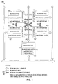
- a highly parallel processor comprises an array of processing elements (PEs) 110, 120, 130 and 140, and a controller sequence processor (SP) 150.
- PEs processing elements
- SP controller sequence processor
- Each PE and the controller SP may include its own register file and at least one execution unit (typically an integer unit or a floating-point unit), a load/store unit, or an interconnection network between PEs. Instruction decode and control logic are also included.
- the controller SP also includes the hardware necessary to support instruction address generation, instruction fetching and decoding, instruction dispatching to the PE array 100 in an instruction sequencer 151 which is preferably included as one of the functional units 152 of SP 150, and to provide overall program control.
- the PEs rely on an interconnection network 160 to exchange data between their register files and a dedicated data bus 170 to exchange data between their register files and the controller SP's register file.
- array instructions are executed on the array of PEs and control instructions in the controller SP, but not simultaneously on both in typical SIMD types of systems. More specifically, PE-parallel SIMD instructions are executed in the array of PEs and SISD instructions are executed in the controller SP.
- the array 100 may be adopted for use in conjunction with the present invention as described further below.
- 60/071,248 entitled “Methods and Apparatus to Dynamically Expand the Instruction Pipeline of a Very Long Instruction Word Processor” filed January 12, 1998
- Provisional Application Serial No. 60/072,915 entitled “Methods and Apparatus to Support Conditional Execution in a VLIW-Based Array Processor with Subword Execution filed January 28, 1988
- Provisional Application Serial No. 60/088,148 entitled “Methods and Apparatus for ManArray PE-PE Switch Control” filed on June 5, 1998
- Provisional Application Serial No. 60,092,148 entitled “Methods and Apparatus for Dynamic Instruction Controlled Reconfigurable Register File with Extended Precision” filed on July 9, 1998
- Provisional Application Serial No. 60/092,130 entitled “Methods and Apparatus for Instruction Addressing in Indirect VLIW Processors” filed on July 9, 1998, all of which are assigned to the assignee of the present invention and incorporated herein by reference in their entirety.
- the present invention provides a dynamic merging processor (DP) capable of dynamically supporting two independent modes of operation and a third unique combined mode of operation in a highly parallel processor comprising an array of processing elements.
- the third combined mode of operation can be used on highly parallel processors with a very long instruction word (VLIW) architecture given this invention.
- Dynamically changing modes of operation is defined as modes that can be changed cycle by cycle under programmer control.
- a combined mode of operation means that in any cycle the two independent modes of operation can be in effect governed by the indirect VLIW (iVLIW) architecture.
- the DP acts as one of the processing elements in the array and participates in the execution of single-instruction-multipie-data (SIMD) instructions.
- SIMD single-instruction-multipie-data
- an array 200 shown in Fig. 2 includes DP 210 and PEs 220, 230 and 240.
- DP 210 has a plurality of execution units or functional units 21 which include an instruction sequencer 214.
- DP 210 also includes two general-purpose register files labeled PE register file 212 and SP register file 213, respectively.
- the execution units are "shared” in that they can execute instructions while the processor is in either of the first two modes of operation separately or combined in the third mode of operation.
- the register files are generally "not shared” in the two separate modes of operation. However, both register files are available for data communications via the array's interconnection network in either mode of operation. By allowing the use of the array's interconnection network as a direct communication path between any PE register file and the SP register file, this structure eliminates the need for a dedicated PE-to-SP data bus. With the ManArray Interconnection Network, the SP is able to broadcast data to the PEs and Receive data from individual PEs in the network.
- the third combined mode of operation can be obtained by intermixing SP and PE instructions in a VLIW.
- the execution units can be shared between SIMD PE operations and SP SISD operations simultaneously on a cycle by cycle basis all under programmers control with no hazards of operation. This sharing of execution units represents a significant savings in implementation costs. Due to application needs it is possible to have an SP to PE Load Broadcast bus but still not require a PE to SP bus path. This is to improve concurrency of data distribution operation to the array of PEs and thereby improve performance.
- Instruction processing begins with an instruction sequencer 214 in Fig. 2 of the DP fetching instructions. After each instruction is fetched, it is decoded in parallel by the DP and by each PE in the array. It is noted that an alternative exists to predecode the SP/PE bit to determine whether the instruction should be dispatched to the rest of the PEs or not. In either case and, in each device, a "mode-of-operation" bit in the instruction word is examined to determine the mode of operation (i.e. "PE" or "SP") in which the instruction should be executed.
- a suggested instruction format 300 is shown in Fig. 3 .
- the mode-of-operation bit is set to a logic "1"
- a PE mode of operation is indicated.
- an SP mode of operation is indicated.
- every PE in the array, and the DP, acting as another processing element of the array executes the instruction.
- the SP mode of operation is indicated, only the DP, acting as the controlling element of the array, executes the instruction.
- the SP and PE modes of operation can be mixed producing unlimited programming flexibility within the capability of the iVLIW or the VLIWarchitecture.
- the mode-of-operation bit is also used to select which register file is used for the operation. For instance, if the instruction is an integer ADD instruction, the mode-of-operation bit is used to determine the register file in which the source and destination registers are located.
- a logical view of the register file selection mechanism 400 is illustrated in Fig. 4 .
- an array 500 includes a DP 510 and PEs 520, 530 and 540.
- the DP 510 includes a plurality of execution units and a single general-purpose register file.
- the execution units are "shared" in that they can execute instructions while the processor is in either mode of operation.
- the register file is divided into two banks, a PE bank and a SP bank, where the two banks are generally "not shared” in the two separate modes of operation. However, both banks are available for data communications in either mode of operation via the array's interconnection network, enabling the exchange of data between PEs or a PE and the SP.
- Instruction processing begins with an instruction sequencer 511 which is a part of the functional units block 512 of the DP 510 which operates to fetch instructions. After each instruction is fetched, it is decoded in parallel by the DP and by each PE in the array. In each device, a "mode-of-operation" bit in the instruction word is examined to determine the mode of operation (i.e. "PE” or "SP") in which the instruction should be executed. If the mode-of operation bit is set to a logic "1", a PE mode of operation is indicated. If the mode-of-operation bit is set to a logic "0", an SP mode of operation is indicated. If the PE mode of operation is indicated, every PE in the array, and the DP, acting as another processing element of the array, executes the instruction. If the SP mode of operation is indicated, only the DP, acting as the controlling element of the array, executes the instruction.
- PE mode-of-operation bit in the instruction word is examined to determine the mode of operation (i.e. "PE” or "SP") in which
- the mode-of-operation bit is also used to enable the appropriate register bank for the operation.
- the mode-of-operation bit is used to enable the register bank in which the source and destination registers are located.
- a logical view of a suitable register bank selection mechanism 600 is illustrated in Fig. 6 .
- Register files are typically custom designed which might provide an advantage to the approach of Fig. 6 versus the approach of Fig. 4 . This is an implementation and technology process decision.
- the DP, the array of PE's, and their interconnection network are implemented in a manner similar to that described in the first and second embodiments of the present invention, respectively.
- the most-significant bit (MSB) of the source and/or destination register addresses contained in the instruction is used.
- a suggested instruction format 700 for the operation of these embodiments is shown in Fig. 7 .
- Instruction processing begins with the instruction sequencer in the DP fetching instructions. As each instruction is fetched, it is decoded in parallel by the DP and by each PE in the array. In each device, the MSB of the source and/or target register addresses in the instruction word is examined to determine the mode of operation (i.e. "PE" or "SI'") in which the instruction should be executed. If all of the MSBs are set to a logic "1", a PE mode of operation is indicated. If all of the MSBs are set to a logic "0", an SP mode of operation is indicated. If the PE mode of operation is indicated, all of the PEs in the array, and the DP, acting as another processing element of the array, execute the instruction. If the SP mode of operation is indicated, only the DP, acting as the controlling element of the array, executes the instruction.
- PE the mode of operation
- the instruction contains more than one register address (e.g. a source address and a destination address, or two source addresses and one destination address), and the MSBs in at least two addresses are not the same, then in an array processor consisting of a DP and multiple PEs the MSB of the Destination Register Address determines whether the instruction is a control or PE instruction.
- the MSBs are used to select (or enable) the appropriate file (or bank) for the operation.
- the MSBs bit are used to select (or enable) the register files (or banks) in which the source and destination registers are located.
- a logical view of a suitable register file selection mechanism 800 is illustrated in Fig. 8 .
- controller SISD instructions to be executed concurrently with SIMD PE instructions. This is preferably accomplished using the ManArray iVLIW architecture.
- SP/PE mode of operation bit in each simplex instruction an iVLIW containing at least two simplex instructions can mix SP instructions with PE instructions. This powerful feature allows sequential code to be intermixed with highly parallel code thereby further optimizing performance in an array processor.
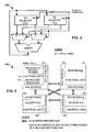
- a VLIW decode and control logic block 910 containing a minimum of two registered simplex instructions provides the write enable control signals 912 and 914 to the SP register file 970 and the PE register file 980.
- Signals 912 and 916 are generated from the decode and control logic block 930 and the signals 914 and 918 are generated from the decode and control logic block 935.
- the iVLIW simplex instruction mode-of-operation bit 915 controls which register file the results from function 1 945 or function 2 955 are to be written, at the end of execution.
- the inverters 960 logically indicate a single level control over which register file is written to and controls operation so that only one register file is written to at a time.
- the multiplexers 940 and 950 control the source data path from the appropriate register file to the inputs of the functional units based upon multiplexer enable signals 916 and 918 respectively.
Abstract
Description
- The present invention relates generally to improvements to array processing, and more particularly, to advantageous techniques for providing dual mode operation of a processor as both a control element for an array and as a processing element in the array.
- Separate control and processing elements are seen in a variety of parallel processing arrays. Such elements are typically dedicated to defined control or processing tasks. Various aspects of such arrangements result in overall system inefficiencies.
- The present invention recognizes that typically in the prior art when a Single Instruction Multiple Data stream (SIMD) instruction is executed, only the array's Processing Element's (PE's) resources are used, except for the controller Sequence Processor's (SP's) address generation resources, and when a Single Instruction Single Data (SISD) instruction is executed, only the controller SP's resources are used thereby keeping the controller resources separate from the SIMD array resources. The present invention advantageously combines a PE and the controller SP into a single device, eliminates a dedicated PE-to-SP data bus by taking advantage of this fact, and allows the combined unit to share a single set of execution units thereby reducing implementation costs. With the present invention, an SP controller SISD instruction can be executed in parallel with a SIMD PE instruction.
- These and other features, aspects and advantages of the invention will be apparent to those of skill in the art from the following detailed description taken together with the accompanying drawings.
-
-
Fig. 1 illustrates an SIMD array of PEs controlled by a controller SP with a dedicated PE-to-SP data bus; -
Fig. 2 illustrates a first embodiment of an array in accordance with the present invention including a dual processor and eliminating the dedicated PE-to-SP data bus ofFig. 1 ; -
Fig. 3 illustrates an instruction format for use in conjunction with the array ofFig. 2 ; -
Fig. 4 illustrates a first register file selection mechanism in accordance with the present invention; -
Fig. 5 illustrates a second embodiment of an array in accordance with the present invention; -
Fig. 6 illustrates a second register file selection mechanism in accordance with the present invention; and -
Fig. 7 illustrates an instruction format for use in conjunction with the array and register file selection mechanisms ofFigs. 5 and6 , respectively; -
Fig. 8 illustrates an alternative register file selection mechanism; and -
Fig. 9 illustrates the dynamic VLIW merge capability of the array controller with an array processing element. - In an
array 100 shown inFig. 1 , a highly parallel processor comprises an array of processing elements (PEs) 110, 120, 130 and 140, and a controller sequence processor (SP) 150. Each PE and the controller SP may include its own register file and at least one execution unit (typically an integer unit or a floating-point unit), a load/store unit, or an interconnection network between PEs. Instruction decode and control logic are also included. In addition, the controller SP also includes the hardware necessary to support instruction address generation, instruction fetching and decoding, instruction dispatching to thePE array 100 in aninstruction sequencer 151 which is preferably included as one of thefunctional units 152 ofSP 150, and to provide overall program control. The PEs rely on aninterconnection network 160 to exchange data between their register files and adedicated data bus 170 to exchange data between their register files and the controller SP's register file. - With the exception of the address generation functions, which are always performed by the controller SP, array instructions are executed on the array of PEs and control instructions in the controller SP, but not simultaneously on both in typical SIMD types of systems. More specifically, PE-parallel SIMD instructions are executed in the array of PEs and SISD instructions are executed in the controller SP. The
array 100 may be adopted for use in conjunction with the present invention as described further below. - Further details of a presently preferred ManArray architecture which may be utilized in conjunction with the present invention are found in United States Patent Application Serial Nos.
08/885,310 and08/949,122 filed June 30, 1997 and October 10, 1997, respectively, Provisional Application Serial No.60/064,619 60/067,511 60/068,021 60/071,248 60/072,915 60/088,148 60,092,148 60/092,130 - In one aspect, the present invention provides a dynamic merging processor (DP) capable of dynamically supporting two independent modes of operation and a third unique combined mode of operation in a highly parallel processor comprising an array of processing elements. The third combined mode of operation can be used on highly parallel processors with a very long instruction word (VLIW) architecture given this invention. Dynamically changing modes of operation is defined as modes that can be changed cycle by cycle under programmer control. A combined mode of operation means that in any cycle the two independent modes of operation can be in effect governed by the indirect VLIW (iVLIW) architecture. In a first mode of operation, the DP acts as one of the processing elements in the array and participates in the execution of single-instruction-multipie-data (SIMD) instructions. In a second mode of operation, the DP acts as the controlling element for the array and executes single-instruction-single-data (SISD) instructions. In the third mode of operation, the DP acts simultaneously as the controlling element for the array and as one of the processing elements in the array. This is accomplished when the DP executes an iVLIW instruction containing a combination of SP SISD and PE SIMD type of instructions. To support these three modes of operation, in one presently preferred embodiment of the present invention, an
array 200 shown inFig. 2 includesDP 210 andPEs instruction sequencer 214. DP 210 also includes two general-purpose register files labeledPE register file 212 andSP register file 213, respectively. The execution units are "shared" in that they can execute instructions while the processor is in either of the first two modes of operation separately or combined in the third mode of operation. The register files are generally "not shared" in the two separate modes of operation. However, both register files are available for data communications via the array's interconnection network in either mode of operation. By allowing the use of the array's interconnection network as a direct communication path between any PE register file and the SP register file, this structure eliminates the need for a dedicated PE-to-SP data bus. With the ManArray Interconnection Network, the SP is able to broadcast data to the PEs and Receive data from individual PEs in the network. The third combined mode of operation can be obtained by intermixing SP and PE instructions in a VLIW. In this manner, the execution units can be shared between SIMD PE operations and SP SISD operations simultaneously on a cycle by cycle basis all under programmers control with no hazards of operation. This sharing of execution units represents a significant savings in implementation costs. Due to application needs it is possible to have an SP to PE Load Broadcast bus but still not require a PE to SP bus path. This is to improve concurrency of data distribution operation to the array of PEs and thereby improve performance. - Instruction processing begins with an
instruction sequencer 214 inFig. 2 of the DP fetching instructions. After each instruction is fetched, it is decoded in parallel by the DP and by each PE in the array. It is noted that an alternative exists to predecode the SP/PE bit to determine whether the instruction should be dispatched to the rest of the PEs or not. In either case and, in each device, a "mode-of-operation" bit in the instruction word is examined to determine the mode of operation (i.e. "PE" or "SP") in which the instruction should be executed. A suggestedinstruction format 300 is shown inFig. 3 . - If the mode-of-operation bit is set to a logic "1", a PE mode of operation is indicated. If the mode-of-operation bit is set to a logic "0", an SP mode of operation is indicated. If the PE mode of operation is indicated, every PE in the array, and the DP, acting as another processing element of the array, executes the instruction. If the SP mode of operation is indicated, only the DP, acting as the controlling element of the array, executes the instruction. In a VLIW or iVLIW processor containing multiple instructions of
format 300 shownFig. 3 , the SP and PE modes of operation can be mixed producing unlimited programming flexibility within the capability of the iVLIW or the VLIWarchitecture. - When an instruction is decoded in the DP, the mode-of-operation bit is also used to select which register file is used for the operation. For instance, if the instruction is an integer ADD instruction, the mode-of-operation bit is used to determine the register file in which the source and destination registers are located. A logical view of the register
file selection mechanism 400 is illustrated inFig. 4 . - In a second embodiment of the present invention shown in
Fig. 5 , anarray 500 includes aDP 510 andPEs DP 510 includes a plurality of execution units and a single general-purpose register file. The execution units are "shared" in that they can execute instructions while the processor is in either mode of operation. The register file is divided into two banks, a PE bank and a SP bank, where the two banks are generally "not shared" in the two separate modes of operation. However, both banks are available for data communications in either mode of operation via the array's interconnection network, enabling the exchange of data between PEs or a PE and the SP. - Instruction processing begins with an
instruction sequencer 511 which is a part of the functional units block 512 of theDP 510 which operates to fetch instructions. After each instruction is fetched, it is decoded in parallel by the DP and by each PE in the array. In each device, a "mode-of-operation" bit in the instruction word is examined to determine the mode of operation (i.e. "PE" or "SP") in which the instruction should be executed. If the mode-of operation bit is set to a logic "1", a PE mode of operation is indicated. If the mode-of-operation bit is set to a logic "0", an SP mode of operation is indicated. If the PE mode of operation is indicated, every PE in the array, and the DP, acting as another processing element of the array, executes the instruction. If the SP mode of operation is indicated, only the DP, acting as the controlling element of the array, executes the instruction. - When an instruction is decoded in the DP, the mode-of-operation bit is also used to enable the appropriate register bank for the operation. For the example of the integer ADD instruction, the mode-of-operation bit is used to enable the register bank in which the source and destination registers are located. A logical view of a suitable register
bank selection mechanism 600 is illustrated inFig. 6 . Register files are typically custom designed which might provide an advantage to the approach ofFig. 6 versus the approach ofFig. 4 . This is an implementation and technology process decision. - In third and fourth embodiments of the present invention, the DP, the array of PE's, and their interconnection network, are implemented in a manner similar to that described in the first and second embodiments of the present invention, respectively. Unlike the implementation of the first two embodiments, however, instead of using a "mode-of operation" bit in the instruction to determine the register file, or bank, accessed by the DP (or PEs) during an operation, the most-significant bit (MSB) of the source and/or destination register addresses contained in the instruction is used. A suggested
instruction format 700 for the operation of these embodiments is shown inFig. 7 . - Instruction processing begins with the instruction sequencer in the DP fetching instructions. As each instruction is fetched, it is decoded in parallel by the DP and by each PE in the array. In each device, the MSB of the source and/or target register addresses in the instruction word is examined to determine the mode of operation (i.e. "PE" or "SI'") in which the instruction should be executed. If all of the MSBs are set to a logic "1", a PE mode of operation is indicated. If all of the MSBs are set to a logic "0", an SP mode of operation is indicated. If the PE mode of operation is indicated, all of the PEs in the array, and the DP, acting as another processing element of the array, execute the instruction. If the SP mode of operation is indicated, only the DP, acting as the controlling element of the array, executes the instruction.
- However, if the instruction contains more than one register address (e.g. a source address and a destination address, or two source addresses and one destination address), and the MSBs in at least two addresses are not the same, then in an array processor consisting of a DP and multiple PEs the MSB of the Destination Register Address determines whether the instruction is a control or PE instruction. When such an instruction is decoded in the DP, the MSBs are used to select (or enable) the appropriate file (or bank) for the operation. For the example of the integer ADD instruction, the MSBs bit are used to select (or enable) the register files (or banks) in which the source and destination registers are located. A logical view of a suitable register
file selection mechanism 800 is illustrated inFig. 8 . - The ability to share execution units in a controller combined with an array processing element allows controller SISD instructions to be executed concurrently with SIMD PE instructions. This is preferably accomplished using the ManArray iVLIW architecture. By using an SP/PE mode of operation bit in each simplex instruction, an iVLIW containing at least two simplex instructions can mix SP instructions with PE instructions. This powerful feature allows sequential code to be intermixed with highly parallel code thereby further optimizing performance in an array processor.
- Suitable apparatus to implement this is shown in
Fig. 9 with twosimplex instructions Fig. 9 and where twofunction units Fig. 9 . a VLIW decode and controllogic block 910 containing a minimum of two registered simplex instructions provides the write enablecontrol signals SP register file 970 and thePE register file 980.Signals 912 and 916 are generated from the decode and controllogic block 930 and thesignals 914 and 918 are generated from the decode and controllogic block 935. The iVLIW simplex instruction mode-of-operation bit 915 (SP/PE) controls which register file the results fromfunction 1 945 orfunction 2 955 are to be written, at the end of execution. Theinverters 960 logically indicate a single level control over which register file is written to and controls operation so that only one register file is written to at a time. Themultiplexers - With this type of mechanism and a combined controller and processing element it is possible to intermix sequential controller instructions with highly parallel SIMD array PE instructions.
- While the present invention has been disclosed in the context of a number of presently preferred embodiments, it will be recognized that many variations may be made to adapt the present teachings to other contexts consistent with the claims which follow.
- This disclosure includes all the subject matter recited in the following clauses:
- 1. A dual mode processor array comprising:
- a control processor; and
- at least one processing element sharing a single set of function units,
- said dual mode processor acting as a processing element in a first mode of operation, and acting as a controlling element in a second mode of operation.
- 2. The apparatus of
clause 1 wherein the control processor comprises a register file and a plurality of functional units, one of the plurality of functional units comprising an instruction sequencer for fetching instructions. - 3. The apparatus of
clause 1 wherein the processing element comprises a register file and a plurality of functional units, the plurality of functional units not including an instruction sequencer. - 4. The apparatus of
clause 1 wherein the dual mode processor is connected with a plurality of processing elements by an interconnection bus to form a processing array. - 5. The apparatus of clause 4 wherein the dual mode processor and the plurality of processing elements further comprise register files and the interconnection bus is utilized as a direct communication path between any processing element register file and any register file in the dual mode processor utilized in said second mode.
- 6. The apparatus of
clause 1 wherein the control processing of the dual mode processor further comprises instruction fetching, the dual mode processor and the processing element being operable to decode each instruction and to examine a mode of operation bit in the instruction to determine the mode of operation in which the instruction should be executed for instruction execution of control type instructions and instruction execution of PE type instructions. - 7. The apparatus of clause 4 further comprising a register file selection mechanism.
- 8. The apparatus of clause 4 wherein the dual mode processor and the processing elements further comprise a plurality of register files and the plurality of register files of the dual mode processor are organized in banks.
- 9. The apparatus of clause 8 further comprising a register file bank selection mechanism.
- 10. The apparatus of
clause 1 wherein the dual mode processor further comprises an instruction sequence which fetches instructions, the control processor and the processing element being operable to decode each instruction and to examine a most significant bit in the instruction to determine the mode of operation. - 11. A method of operating an array comprising a dual mode processor and a plurality of processing elements connected to the dual mode processor with an interconnection bus, the method comprising the steps of :
- operating the dual mode processor as one of the processing elements in the dual mode array to participate in the execution of single instruction multiple data instructions in a first mode of operation; and
- operating the dual mode processor as a controlling element for the array to execute non-array instructions in a second mode of operation.
- 12. The method of clause 11 further comprising the step of:
- determining the mode of operation of the dual mode processor based upon an examination of a mode of operation bit in an instruction.
- 13. The method of clause 11 further comprising the step of:
- determining the mode of operation of the dual mode processor based upon an examination of the most significant bit in the destination register selection field of an instruction.
- 14. The method of clause 11 further comprising the step of:
- selecting a register file in the dual mode processor utilizing the most significant bit of the register selection fields of an instruction.
- 15. The method of clause 11 further comprising the steps of:
- organizing register files in the dual mode processor in banks; and
- selecting a register file bank in the dual mode processor utilizing a register file bank selection mechanism.
- 16. An apparatus for concurrently executing controller SISD instructions and SIMD processing element instructions comprising:
- a combined controller and processing element;
- at least two simplex instructions each containing a mode of operation bit; and
- very long instruction word (VLIW) containing said at least two simplex instructions.
- 17. The apparatus of clause 16 further comprising a very long instruction word (VLIW) decode and control logic block.
- 18. The apparatus of clause 17 further comprising a sequence processor register file and a processing element register file connected to receive write enable control signals from the VLIW decode and control logic block.
- 19. The apparatus of clause 18 further comprising at least two multiplexers to control the source data path from said register files to inputs of functional units of the combined controller and processing element.
- 20. The apparatus of clause 16 wherein the combined controller and processing element is connected by an interconnection bus to a plurality of processing elements in a manifold array processing architecture.
Claims (14)
- A dual mode processor (210), characterized by:a first function unit (945) and a second function unit (955) both operable to execute processing element (PE) instructions and control processor (CP) instructions;a first register file (RF) (980) and a second RF (970), wherein both RFs are coupled to the first function unit and to the second function unit; anda PE merged with a CP having an instruction sequencer (214), said instruction sequencer operable to fetch an instruction word containing a first instruction (920) and a second instruction (925),wherein said dual mode processor is operable to execute the first instruction according to a first mode of operation value in the first instruction and to execute the second instruction according to a second mode of operation value in the second instruction,wherein the dual mode processor is configurable, by the first mode of operation value, to select one of the two RFs to provide a source operand to the first function unit and to write a result from the first function unit, andwherein the dual mode processor is configurable, by the second mode of operation value, to select one of the two RFs to provide a source operand to the second function unit and to write a result from the second function unit, andwherein dual mode processor is operable to execute the first instruction and the second instruction in parallel.
- The dual mode processor of claim 1, wherein the dual mode processor is configurable, by the first mode of operation value, to operate as a PE to select the first RF in response to the first instruction being a PE instruction and the dual mode processor is configurable, by the second mode of operation value, to operate as a PE to select the first RF in response to the second instruction being a PE instruction.
- The dual mode processor of claim 1, wherein the dual mode processor is configurable, by the first mode of operation value, to operate as a CP to select the second RF in response to the first instruction being a CP instruction and the dual mode processor is configurable, by the second mode of operation value, to operate as a CP to select the second RF in response to the second instruction being a CP instruction.
- The dual mode processor of claim 1, wherein the dual mode processor is configurable, by the first mode of operation value, to operate as a PE to select the first RF in response to the first instruction being a PE instruction and the dual mode processor is configurable, by the second mode of operation value, to operate as a CP to select the second RF in response to the second instruction being a CP instruction.
- The dual mode processor of claim 1, wherein the first mode of operation value is a bit (915) in the first instruction (920) and the second mode of operation value is a bit (915) in the second instruction (925).
- The dual mode processor of claim 1, wherein the first mode of operation value is a most significant bit (MSB) of a destination register file address field in the first instruction and the second mode of operation value is an MSB of a destination register file address field in the second instruction.
- The dual mode processor of claim 1, wherein the dual mode processor is coupled to a plurality of PEs by an interconnection bus to form a processing array.
- A method of operating a dual mode processor (210), the method characterized by the steps of:fetching an instruction word containing a first instruction (920) and a second instruction (925);executing the first instruction (920) according to a first mode of operation value in the first instruction, wherein the dual mode processor is configurable, by the first mode of operation value, to select one of two register files (RFs) (980, 970) to provide a source operand to a first function unit (945) and to write a result from the first function unit (945); andexecuting the second instruction (925) according to a second mode of operation value in the second instruction, wherein the dual mode processor is configurable, by the second mode of operation value, to select one of the two RFs (980, 970) to provide a source operand to a second function unit (955) and to write a result from the second function unit (955),wherein the dual mode processor is operable to execute the first instruction and the second instruction in parallel.
- The method of claim 8, wherein the dual mode processor is configurable, by the first mode of operation value, to operate as a processing element (PE) to select the first RF in response to the first instruction being a PE instruction and the dual mode processor is configurable, by the second mode of operation value, to operate as a PE to select the first RF in response to the second instruction being a PE instruction.
- The method of claim 9, further comprising:dispatching the instruction word to a plurality of PEs coupled to the dual mode processor by an instruction bus and by an interconnection data bus to form a processing array.
- The method of claim 8, wherein the dual mode processor is configurable, by the first mode of operation value, to operate as a control processor (CP) to select the second RF in response to the first instruction being a CP instruction and the dual mode processor is configurable, by the second mode of operation value, to operate as a CP to select the second RF in response to the second instruction being a CP instruction.
- The method of claim 8, wherein the dual mode processor is configurable, by the first mode of operation value, to operate as a PE to select the first RF in response to the first instruction being a PE instruction and the dual mode processor is configurable, by the second mode of operation value, to operate as a CP to select the second RF in response to the second instruction being a CP instruction.
- The method of claim 8, wherein the first mode of operation value is a bit in the first instruction and the second mode of operation value is a bit in the second instruction.
- The method of claim 8, wherein the first mode of operation value is a most significant bit (MSB) of a destination register file address field in the first instruction and the second mode of operation value is an MSB of a destination register file address field in the second instruction.
Applications Claiming Priority (2)
| Application Number | Priority Date | Filing Date | Title |
|---|---|---|---|
| US09/169,072 US6219776B1 (en) | 1998-03-10 | 1998-10-09 | Merged array controller and processing element |
| EP99953109A EP1127316B1 (en) | 1998-10-09 | 1999-10-08 | Methods and apparatus for dynamically merging an array controller with an array processing element |
Related Parent Applications (1)
| Application Number | Title | Priority Date | Filing Date |
|---|---|---|---|
| EP99953109.8 Division | 1999-10-08 |
Publications (3)
| Publication Number | Publication Date |
|---|---|
| EP2336879A2 true EP2336879A2 (en) | 2011-06-22 |
| EP2336879A3 EP2336879A3 (en) | 2011-07-06 |
| EP2336879B1 EP2336879B1 (en) | 2013-03-06 |
Family
ID=22614163
Family Applications (2)
| Application Number | Title | Priority Date | Filing Date |
|---|---|---|---|
| EP11002227A Expired - Lifetime EP2336879B1 (en) | 1998-10-09 | 1999-10-08 | Methods and apparatus for dynamically merging an array controller with an array processing element |
| EP99953109A Expired - Lifetime EP1127316B1 (en) | 1998-10-09 | 1999-10-08 | Methods and apparatus for dynamically merging an array controller with an array processing element |
Family Applications After (1)
| Application Number | Title | Priority Date | Filing Date |
|---|---|---|---|
| EP99953109A Expired - Lifetime EP1127316B1 (en) | 1998-10-09 | 1999-10-08 | Methods and apparatus for dynamically merging an array controller with an array processing element |
Country Status (5)
| Country | Link |
|---|---|
| US (3) | US6219776B1 (en) |
| EP (2) | EP2336879B1 (en) |
| JP (2) | JP4417567B2 (en) |
| AT (1) | ATE534073T1 (en) |
| WO (1) | WO2000022535A1 (en) |
Families Citing this family (82)
| Publication number | Priority date | Publication date | Assignee | Title |
|---|---|---|---|---|
| JP3541669B2 (en) * | 1998-03-30 | 2004-07-14 | 松下電器産業株式会社 | Arithmetic processing unit |
| US6988181B2 (en) * | 2000-03-08 | 2006-01-17 | Sun Microsystems, Inc. | VLIW computer processing architecture having a scalable number of register files |
| JP3987784B2 (en) * | 2002-10-30 | 2007-10-10 | Necエレクトロニクス株式会社 | Array type processor |
| KR20050089084A (en) * | 2002-12-30 | 2005-09-07 | 코닌클리즈케 필립스 일렉트로닉스 엔.브이. | A method for accessing a bus in a clustered instruction level parallelism processor |
| EP1581884A2 (en) * | 2002-12-30 | 2005-10-05 | Koninklijke Philips Electronics N.V. | Processing system |
| US7437729B2 (en) * | 2003-04-23 | 2008-10-14 | Micron Technology, Inc. | Method for load balancing a loop of parallel processing elements |
| US7503046B2 (en) * | 2003-04-23 | 2009-03-10 | Micron Technology, Inc. | Method of obtaining interleave interval for two data values |
| US7263543B2 (en) * | 2003-04-23 | 2007-08-28 | Micron Technology, Inc. | Method for manipulating data in a group of processing elements to transpose the data using a memory stack |
| US7437726B2 (en) * | 2003-04-23 | 2008-10-14 | Micron Technology, Inc. | Method for rounding values for a plurality of parallel processing elements |
| US7596678B2 (en) * | 2003-04-23 | 2009-09-29 | Micron Technology, Inc. | Method of shifting data along diagonals in a group of processing elements to transpose the data |
| US7581080B2 (en) * | 2003-04-23 | 2009-08-25 | Micron Technology, Inc. | Method for manipulating data in a group of processing elements according to locally maintained counts |
| US7913062B2 (en) | 2003-04-23 | 2011-03-22 | Micron Technology, Inc. | Method of rotating data in a plurality of processing elements |
| US7574466B2 (en) * | 2003-04-23 | 2009-08-11 | Micron Technology, Inc. | Method for finding global extrema of a set of shorts distributed across an array of parallel processing elements |
| US7373645B2 (en) * | 2003-04-23 | 2008-05-13 | Micron Technology, Inc. | Method for using extrema to load balance a loop of parallel processing elements |
| US7448038B2 (en) * | 2003-04-23 | 2008-11-04 | Micron Technology, Inc. | Method for using filtering to load balance a loop of parallel processing elements |
| US7430742B2 (en) | 2003-04-23 | 2008-09-30 | Micron Technology, Inc. | Method for load balancing a line of parallel processing elements |
| US7454451B2 (en) | 2003-04-23 | 2008-11-18 | Micron Technology, Inc. | Method for finding local extrema of a set of values for a parallel processing element |
| US7676648B2 (en) * | 2003-04-23 | 2010-03-09 | Micron Technology, Inc. | Method for manipulating data in a group of processing elements to perform a reflection of the data |
| US7472392B2 (en) * | 2003-04-23 | 2008-12-30 | Micron Technology, Inc. | Method for load balancing an n-dimensional array of parallel processing elements |
| US7447720B2 (en) | 2003-04-23 | 2008-11-04 | Micron Technology, Inc. | Method for finding global extrema of a set of bytes distributed across an array of parallel processing elements |
| GB2409060B (en) * | 2003-12-09 | 2006-08-09 | Advanced Risc Mach Ltd | Moving data between registers of different register data stores |
| GB2409068A (en) * | 2003-12-09 | 2005-06-15 | Advanced Risc Mach Ltd | Data element size control within parallel lanes of processing |
| US7383427B2 (en) * | 2004-04-22 | 2008-06-03 | Sony Computer Entertainment Inc. | Multi-scalar extension for SIMD instruction set processors |
| US7401206B2 (en) * | 2004-06-30 | 2008-07-15 | Sun Microsystems, Inc. | Apparatus and method for fine-grained multithreading in a multipipelined processor core |
| JP4477959B2 (en) * | 2004-07-26 | 2010-06-09 | 独立行政法人理化学研究所 | Arithmetic processing device for broadcast parallel processing |
| WO2006033078A2 (en) | 2004-09-22 | 2006-03-30 | Koninklijke Philips Electronics N.V. | Data processing circuit wherein functional units share read ports |
| US7493474B1 (en) * | 2004-11-10 | 2009-02-17 | Altera Corporation | Methods and apparatus for transforming, loading, and executing super-set instructions |
| EP2477109B1 (en) | 2006-04-12 | 2016-07-13 | Soft Machines, Inc. | Apparatus and method for processing an instruction matrix specifying parallel and dependent operations |
| US7730280B2 (en) * | 2006-06-15 | 2010-06-01 | Vicore Technologies, Inc. | Methods and apparatus for independent processor node operations in a SIMD array processor |
| US8572354B2 (en) | 2006-09-28 | 2013-10-29 | 3Dlabs Inc., Ltd. | Programmable logic unit and method for translating and processing instructions using interpretation registers |
| EP2523101B1 (en) | 2006-11-14 | 2014-06-04 | Soft Machines, Inc. | Apparatus and method for processing complex instruction formats in a multi- threaded architecture supporting various context switch modes and virtualization schemes |
| KR100896269B1 (en) | 2006-12-05 | 2009-05-08 | 한국전자통신연구원 | Simd parallel processor with simd/sisd/row/column opertaion modes |
| US20080133879A1 (en) * | 2006-12-05 | 2008-06-05 | Electronics And Telecommunications Research Institute | SIMD parallel processor with SIMD/SISD/row/column operation modes |
| US7739481B1 (en) * | 2007-09-06 | 2010-06-15 | Altera Corporation | Parallelism with variable partitioning and threading |
| US7809925B2 (en) * | 2007-12-07 | 2010-10-05 | International Business Machines Corporation | Processing unit incorporating vectorizable execution unit |
| US9164945B2 (en) * | 2008-12-01 | 2015-10-20 | Micron Technology, Inc. | Devices, systems, and methods to synchronize parallel processing of a single data stream |
| US20100138575A1 (en) | 2008-12-01 | 2010-06-03 | Micron Technology, Inc. | Devices, systems, and methods to synchronize simultaneous dma parallel processing of a single data stream by multiple devices |
| US8140780B2 (en) * | 2008-12-31 | 2012-03-20 | Micron Technology, Inc. | Systems, methods, and devices for configuring a device |
| US20100174887A1 (en) | 2009-01-07 | 2010-07-08 | Micron Technology Inc. | Buses for Pattern-Recognition Processors |
| EP2254280A1 (en) * | 2009-05-19 | 2010-11-24 | Electrolux Home Products Corporation N.V. | Bus control for a domestic appliance |
| TWI414994B (en) * | 2009-09-24 | 2013-11-11 | Ind Tech Res Inst | Configurable processing apparatus and system thereof |
| US9323994B2 (en) | 2009-12-15 | 2016-04-26 | Micron Technology, Inc. | Multi-level hierarchical routing matrices for pattern-recognition processors |
| KR101738941B1 (en) * | 2010-03-23 | 2017-05-24 | 삼성전자주식회사 | Reconfigurable array and control method of reconfigurable array |
| EP2616928B1 (en) | 2010-09-17 | 2016-11-02 | Soft Machines, Inc. | Single cycle multi-branch prediction including shadow cache for early far branch prediction |
| WO2012135031A2 (en) | 2011-03-25 | 2012-10-04 | Soft Machines, Inc. | Executing instruction sequence code blocks by using virtual cores instantiated by partitionable engines |
| EP2689326B1 (en) | 2011-03-25 | 2022-11-16 | Intel Corporation | Memory fragments for supporting code block execution by using virtual cores instantiated by partitionable engines |
| WO2012135041A2 (en) | 2011-03-25 | 2012-10-04 | Soft Machines, Inc. | Register file segments for supporting code block execution by using virtual cores instantiated by partitionable engines |
| WO2012162189A1 (en) | 2011-05-20 | 2012-11-29 | Soft Machines, Inc. | An interconnect structure to support the execution of instruction sequences by a plurality of engines |
| CN103649932B (en) | 2011-05-20 | 2017-09-26 | 英特尔公司 | The scattered distribution of resource and for supporting by the interconnection structure of multiple engine execute instruction sequences |
| KR101703401B1 (en) | 2011-11-22 | 2017-02-06 | 소프트 머신즈, 인크. | An accelerated code optimizer for a multiengine microprocessor |
| US20150039859A1 (en) | 2011-11-22 | 2015-02-05 | Soft Machines, Inc. | Microprocessor accelerated code optimizer |
| SE1151231A1 (en) * | 2011-12-20 | 2013-05-07 | Mediatek Sweden Ab | Digital signal processor and baseband communication device |
| US20130275709A1 (en) | 2012-04-12 | 2013-10-17 | Micron Technology, Inc. | Methods for reading data from a storage buffer including delaying activation of a column select |
| US9524248B2 (en) | 2012-07-18 | 2016-12-20 | Micron Technology, Inc. | Memory management for a hierarchical memory system |
| US9811342B2 (en) | 2013-03-15 | 2017-11-07 | Intel Corporation | Method for performing dual dispatch of blocks and half blocks |
| US9891924B2 (en) | 2013-03-15 | 2018-02-13 | Intel Corporation | Method for implementing a reduced size register view data structure in a microprocessor |
| KR102083390B1 (en) | 2013-03-15 | 2020-03-02 | 인텔 코포레이션 | A method for emulating a guest centralized flag architecture by using a native distributed flag architecture |
| US9703574B2 (en) | 2013-03-15 | 2017-07-11 | Micron Technology, Inc. | Overflow detection and correction in state machine engines |
| US10140138B2 (en) | 2013-03-15 | 2018-11-27 | Intel Corporation | Methods, systems and apparatus for supporting wide and efficient front-end operation with guest-architecture emulation |
| WO2014150971A1 (en) | 2013-03-15 | 2014-09-25 | Soft Machines, Inc. | A method for dependency broadcasting through a block organized source view data structure |
| WO2014150991A1 (en) | 2013-03-15 | 2014-09-25 | Soft Machines, Inc. | A method for implementing a reduced size register view data structure in a microprocessor |
| US9569216B2 (en) | 2013-03-15 | 2017-02-14 | Soft Machines, Inc. | Method for populating a source view data structure by using register template snapshots |
| KR102063656B1 (en) | 2013-03-15 | 2020-01-09 | 소프트 머신즈, 인크. | A method for executing multithreaded instructions grouped onto blocks |
| US9886279B2 (en) | 2013-03-15 | 2018-02-06 | Intel Corporation | Method for populating and instruction view data structure by using register template snapshots |
| US10275255B2 (en) | 2013-03-15 | 2019-04-30 | Intel Corporation | Method for dependency broadcasting through a source organized source view data structure |
| US9448965B2 (en) | 2013-03-15 | 2016-09-20 | Micron Technology, Inc. | Receiving data streams in parallel and providing a first portion of data to a first state machine engine and a second portion to a second state machine |
| WO2014150806A1 (en) | 2013-03-15 | 2014-09-25 | Soft Machines, Inc. | A method for populating register view data structure by using register template snapshots |
| US9904625B2 (en) | 2013-03-15 | 2018-02-27 | Intel Corporation | Methods, systems and apparatus for predicting the way of a set associative cache |
| US11366675B2 (en) | 2014-12-30 | 2022-06-21 | Micron Technology, Inc. | Systems and devices for accessing a state machine |
| US10430210B2 (en) | 2014-12-30 | 2019-10-01 | Micron Technology, Inc. | Systems and devices for accessing a state machine |
| US10769099B2 (en) | 2014-12-30 | 2020-09-08 | Micron Technology, Inc. | Devices for time division multiplexing of state machine engine signals |
| US10175961B2 (en) * | 2015-06-10 | 2019-01-08 | International Business Machines Corporation | Joining operator graph elements via whole program optimization |
| US10977309B2 (en) | 2015-10-06 | 2021-04-13 | Micron Technology, Inc. | Methods and systems for creating networks |
| US10846103B2 (en) | 2015-10-06 | 2020-11-24 | Micron Technology, Inc. | Methods and systems for representing processing resources |
| US10691964B2 (en) | 2015-10-06 | 2020-06-23 | Micron Technology, Inc. | Methods and systems for event reporting |
| US10146555B2 (en) | 2016-07-21 | 2018-12-04 | Micron Technology, Inc. | Adaptive routing to avoid non-repairable memory and logic defects on automata processor |
| US10268602B2 (en) | 2016-09-29 | 2019-04-23 | Micron Technology, Inc. | System and method for individual addressing |
| US10019311B2 (en) | 2016-09-29 | 2018-07-10 | Micron Technology, Inc. | Validation of a symbol response memory |
| US10592450B2 (en) | 2016-10-20 | 2020-03-17 | Micron Technology, Inc. | Custom compute cores in integrated circuit devices |
| US10929764B2 (en) | 2016-10-20 | 2021-02-23 | Micron Technology, Inc. | Boolean satisfiability |
| US10372507B2 (en) * | 2016-12-31 | 2019-08-06 | Intel Corporation | Compute engine architecture to support data-parallel loops with reduction operations |
| US20220100699A1 (en) * | 2020-09-30 | 2022-03-31 | Beijing Tsingmicro Intelligent Technology Co., Ltd. | Computing array and processor having the same |
Citations (8)
| Publication number | Priority date | Publication date | Assignee | Title |
|---|---|---|---|---|
| US6461997B1 (en) | 1999-01-14 | 2002-10-08 | Monsanto Technology Llc | Triazole sulfones having herbicidal activity |
| US6751197B1 (en) | 1998-10-19 | 2004-06-15 | Sony Corporation | Information processing apparatus and method, and provision medium |
| US6802197B2 (en) | 2002-01-09 | 2004-10-12 | Barrera Maria Eugenia | Process for manufacturing a high strength container, particularly an aerosol container, and the container obtained through such process |
| US7124898B2 (en) | 2001-04-26 | 2006-10-24 | Dci Marketing, Inc. | Merchandising system |
| US7291588B2 (en) | 1996-10-31 | 2007-11-06 | Chiron Srl | Immunogenic detoxified mutant E. coli LT-A toxin |
| US8814898B2 (en) | 2012-02-21 | 2014-08-26 | Allurion Techologies, Inc. | Methods and devices for deploying and releasing a temporary implant within the body |
| US9213098B2 (en) | 2012-09-12 | 2015-12-15 | Moises Jaime RODRICH | Method and device for detecting presence of vehicle in parking space |
| US9214898B2 (en) | 2013-01-31 | 2015-12-15 | Realtek Semiconductor Corp. | Triple cascode power amplifier |
Family Cites Families (18)
| Publication number | Priority date | Publication date | Assignee | Title |
|---|---|---|---|---|
| US4558411A (en) * | 1969-05-19 | 1985-12-10 | Burroughs Corp. | Polymorphic programmable units employing plural levels of sub-instruction sets |
| GB8329509D0 (en) * | 1983-11-04 | 1983-12-07 | Inmos Ltd | Computer |
| US4783738A (en) * | 1986-03-13 | 1988-11-08 | International Business Machines Corporation | Adaptive instruction processing by array processor having processor identification and data dependent status registers in each processing element |
| CN1008018B (en) * | 1986-09-27 | 1990-05-16 | 徐肇昌 | Cecomputer and its method of cooperation |
| JPH02297684A (en) * | 1989-05-11 | 1990-12-10 | Nec Corp | Microcomputer |
| US5239654A (en) * | 1989-11-17 | 1993-08-24 | Texas Instruments Incorporated | Dual mode SIMD/MIMD processor providing reuse of MIMD instruction memories as data memories when operating in SIMD mode |
| CA2073516A1 (en) * | 1991-11-27 | 1993-05-28 | Peter Michael Kogge | Dynamic multi-mode parallel processor array architecture computer system |
| US5596755A (en) * | 1992-11-03 | 1997-01-21 | Microsoft Corporation | Mechanism for using common code to handle hardware interrupts in multiple processor modes |
| US5511212A (en) * | 1993-06-10 | 1996-04-23 | Rockoff; Todd E. | Multi-clock SIMD computer and instruction-cache-enhancement thereof |
| US5682491A (en) * | 1994-12-29 | 1997-10-28 | International Business Machines Corporation | Selective processing and routing of results among processors controlled by decoding instructions using mask value derived from instruction tag and processor identifier |
| US5649135A (en) | 1995-01-17 | 1997-07-15 | International Business Machines Corporation | Parallel processing system and method using surrogate instructions |
| US5805486A (en) * | 1995-11-28 | 1998-09-08 | Intel Corporation | Moderately coupled floating point and integer units |
| US6088783A (en) * | 1996-02-16 | 2000-07-11 | Morton; Steven G | DPS having a plurality of like processors controlled in parallel by an instruction word, and a control processor also controlled by the instruction word |
| JP3623840B2 (en) * | 1996-01-31 | 2005-02-23 | 株式会社ルネサステクノロジ | Data processing apparatus and microprocessor |
| JP3790607B2 (en) * | 1997-06-16 | 2006-06-28 | 松下電器産業株式会社 | VLIW processor |
| CN100380313C (en) * | 1997-11-07 | 2008-04-09 | 博普斯公司 | Method and apparatus for efficient synchronous MIMD operation with ivLIM PE-to-PE communication |
| US6081884A (en) * | 1998-01-05 | 2000-06-27 | Advanced Micro Devices, Inc. | Embedding two different instruction sets within a single long instruction word using predecode bits |
| US7291598B2 (en) | 2005-01-04 | 2007-11-06 | Gp Medical, Inc. | Nanoparticles for protein drug delivery |
-
1998
- 1998-10-09 US US09/169,072 patent/US6219776B1/en not_active Expired - Lifetime
-
1999
- 1999-10-08 AT AT99953109T patent/ATE534073T1/en active
- 1999-10-08 JP JP2000576374A patent/JP4417567B2/en not_active Expired - Fee Related
- 1999-10-08 WO PCT/US1999/023495 patent/WO2000022535A1/en active Application Filing
- 1999-10-08 EP EP11002227A patent/EP2336879B1/en not_active Expired - Lifetime
- 1999-10-08 EP EP99953109A patent/EP1127316B1/en not_active Expired - Lifetime
-
2001
- 2001-02-14 US US09/783,156 patent/US6606699B2/en not_active Expired - Lifetime
-
2003
- 2003-07-15 US US10/620,144 patent/US6874078B2/en not_active Expired - Fee Related
-
2009
- 2009-07-29 JP JP2009176971A patent/JP4500363B2/en not_active Expired - Fee Related
Patent Citations (8)
| Publication number | Priority date | Publication date | Assignee | Title |
|---|---|---|---|---|
| US7291588B2 (en) | 1996-10-31 | 2007-11-06 | Chiron Srl | Immunogenic detoxified mutant E. coli LT-A toxin |
| US6751197B1 (en) | 1998-10-19 | 2004-06-15 | Sony Corporation | Information processing apparatus and method, and provision medium |
| US6461997B1 (en) | 1999-01-14 | 2002-10-08 | Monsanto Technology Llc | Triazole sulfones having herbicidal activity |
| US7124898B2 (en) | 2001-04-26 | 2006-10-24 | Dci Marketing, Inc. | Merchandising system |
| US6802197B2 (en) | 2002-01-09 | 2004-10-12 | Barrera Maria Eugenia | Process for manufacturing a high strength container, particularly an aerosol container, and the container obtained through such process |
| US8814898B2 (en) | 2012-02-21 | 2014-08-26 | Allurion Techologies, Inc. | Methods and devices for deploying and releasing a temporary implant within the body |
| US9213098B2 (en) | 2012-09-12 | 2015-12-15 | Moises Jaime RODRICH | Method and device for detecting presence of vehicle in parking space |
| US9214898B2 (en) | 2013-01-31 | 2015-12-15 | Realtek Semiconductor Corp. | Triple cascode power amplifier |
Also Published As
| Publication number | Publication date |
|---|---|
| EP2336879A3 (en) | 2011-07-06 |
| EP1127316B1 (en) | 2011-11-16 |
| JP4500363B2 (en) | 2010-07-14 |
| US20040148488A1 (en) | 2004-07-29 |
| WO2000022535A1 (en) | 2000-04-20 |
| JP2010009610A (en) | 2010-01-14 |
| US6606699B2 (en) | 2003-08-12 |
| ATE534073T1 (en) | 2011-12-15 |
| EP1127316A4 (en) | 2008-11-19 |
| US6219776B1 (en) | 2001-04-17 |
| JP2002527823A (en) | 2002-08-27 |
| EP1127316A1 (en) | 2001-08-29 |
| JP4417567B2 (en) | 2010-02-17 |
| US6874078B2 (en) | 2005-03-29 |
| EP2336879B1 (en) | 2013-03-06 |
| US20010032303A1 (en) | 2001-10-18 |
Similar Documents
| Publication | Publication Date | Title |
|---|---|---|
| EP1127316B1 (en) | Methods and apparatus for dynamically merging an array controller with an array processing element | |
| US6581152B2 (en) | Methods and apparatus for instruction addressing in indirect VLIW processors | |
| US7028170B2 (en) | Processing architecture having a compare capability | |
| KR100190738B1 (en) | Parallel processing system and method using surrogate instructions | |
| US5590352A (en) | Dependency checking and forwarding of variable width operands | |
| EP1029266B1 (en) | METHOD AND APPARATUS FOR EFFICIENT SYNCHRONOUS MIMD OPERATIONS WITH iVLIW PE-to-PE COMMUNICATION | |
| US6467036B1 (en) | Methods and apparatus for dynamic very long instruction word sub-instruction selection for execution time parallelism in an indirect very long instruction word processor | |
| US6718457B2 (en) | Multiple-thread processor for threaded software applications | |
| US4992933A (en) | SIMD array processor with global instruction control and reprogrammable instruction decoders | |
| US20110213952A1 (en) | Methods and Apparatus for Dynamic Instruction Controlled Reconfigurable Register File | |
| US20090144502A1 (en) | Meta-Architecture Defined Programmable Instruction Fetch Functions Supporting Assembled Variable Length Instruction Processors | |
| JPH05233569A (en) | Computer system dynamiccaly operated in plurality of modes | |
| JP2010067278A (en) | Methods and apparatus to support conditional execution in processor | |
| US9021236B2 (en) | Methods and apparatus for storing expanded width instructions in a VLIW memory for deferred execution | |
| EP1365318A2 (en) | Microprocessor data manipulation matrix module | |
| EP1027641B1 (en) | Computer processor and method for data streaming | |
| WO2002037269A1 (en) | Fetch and dispatch decoupling mechanism for multistreaming processors | |
| US6883088B1 (en) | Methods and apparatus for loading a very long instruction word memory |
Legal Events
| Date | Code | Title | Description |
|---|---|---|---|
| PUAI | Public reference made under article 153(3) epc to a published international application that has entered the european phase |
Free format text: ORIGINAL CODE: 0009012 |
|
| PUAL | Search report despatched |
Free format text: ORIGINAL CODE: 0009013 |
|
| AC | Divisional application: reference to earlier application |
Ref document number: 1127316 Country of ref document: EP Kind code of ref document: P |
|
| AK | Designated contracting states |
Kind code of ref document: A2 Designated state(s): AT BE CH CY DE DK ES FI FR GB GR IE IT LI LU MC NL PT SE |
|
| AK | Designated contracting states |
Kind code of ref document: A3 Designated state(s): AT BE CH CY DE DK ES FI FR GB GR IE IT LI LU MC NL PT SE |
|
| 17P | Request for examination filed |
Effective date: 20111230 |
|
| 17Q | First examination report despatched |
Effective date: 20120511 |
|
| GRAP | Despatch of communication of intention to grant a patent |
Free format text: ORIGINAL CODE: EPIDOSNIGR1 |
|
| GRAS | Grant fee paid |
Free format text: ORIGINAL CODE: EPIDOSNIGR3 |
|
| GRAA | (expected) grant |
Free format text: ORIGINAL CODE: 0009210 |
|
| AC | Divisional application: reference to earlier application |
Ref document number: 1127316 Country of ref document: EP Kind code of ref document: P |
|
| AK | Designated contracting states |
Kind code of ref document: B1 Designated state(s): AT BE CH CY DE DK ES FI FR GB GR IE IT LI LU MC NL PT SE |
|
| REG | Reference to a national code |
Ref country code: GB Ref legal event code: FG4D |
|
| REG | Reference to a national code |
Ref country code: AT Ref legal event code: REF Ref document number: 599970 Country of ref document: AT Kind code of ref document: T Effective date: 20130315 Ref country code: CH Ref legal event code: EP |
|
| REG | Reference to a national code |
Ref country code: IE Ref legal event code: FG4D |
|
| REG | Reference to a national code |
Ref country code: DE Ref legal event code: R096 Ref document number: 69944658 Country of ref document: DE Effective date: 20130502 |
|
| REG | Reference to a national code |
Ref country code: NL Ref legal event code: T3 |
|
| REG | Reference to a national code |
Ref country code: AT Ref legal event code: MK05 Ref document number: 599970 Country of ref document: AT Kind code of ref document: T Effective date: 20130306 |
|
| PG25 | Lapsed in a contracting state [announced via postgrant information from national office to epo] |
Ref country code: AT Free format text: LAPSE BECAUSE OF FAILURE TO SUBMIT A TRANSLATION OF THE DESCRIPTION OR TO PAY THE FEE WITHIN THE PRESCRIBED TIME-LIMIT Effective date: 20130306 Ref country code: SE Free format text: LAPSE BECAUSE OF FAILURE TO SUBMIT A TRANSLATION OF THE DESCRIPTION OR TO PAY THE FEE WITHIN THE PRESCRIBED TIME-LIMIT Effective date: 20130306 Ref country code: ES Free format text: LAPSE BECAUSE OF FAILURE TO SUBMIT A TRANSLATION OF THE DESCRIPTION OR TO PAY THE FEE WITHIN THE PRESCRIBED TIME-LIMIT Effective date: 20130617 |
|
| PG25 | Lapsed in a contracting state [announced via postgrant information from national office to epo] |
Ref country code: FI Free format text: LAPSE BECAUSE OF FAILURE TO SUBMIT A TRANSLATION OF THE DESCRIPTION OR TO PAY THE FEE WITHIN THE PRESCRIBED TIME-LIMIT Effective date: 20130306 Ref country code: GR Free format text: LAPSE BECAUSE OF FAILURE TO SUBMIT A TRANSLATION OF THE DESCRIPTION OR TO PAY THE FEE WITHIN THE PRESCRIBED TIME-LIMIT Effective date: 20130607 |
|
| PG25 | Lapsed in a contracting state [announced via postgrant information from national office to epo] |
Ref country code: BE Free format text: LAPSE BECAUSE OF FAILURE TO SUBMIT A TRANSLATION OF THE DESCRIPTION OR TO PAY THE FEE WITHIN THE PRESCRIBED TIME-LIMIT Effective date: 20130306 |
|
| PG25 | Lapsed in a contracting state [announced via postgrant information from national office to epo] |
Ref country code: PT Free format text: LAPSE BECAUSE OF FAILURE TO SUBMIT A TRANSLATION OF THE DESCRIPTION OR TO PAY THE FEE WITHIN THE PRESCRIBED TIME-LIMIT Effective date: 20130708 |
|
| PLBE | No opposition filed within time limit |
Free format text: ORIGINAL CODE: 0009261 |
|
| STAA | Information on the status of an ep patent application or granted ep patent |
Free format text: STATUS: NO OPPOSITION FILED WITHIN TIME LIMIT |
|
| PG25 | Lapsed in a contracting state [announced via postgrant information from national office to epo] |
Ref country code: DK Free format text: LAPSE BECAUSE OF FAILURE TO SUBMIT A TRANSLATION OF THE DESCRIPTION OR TO PAY THE FEE WITHIN THE PRESCRIBED TIME-LIMIT Effective date: 20130306 |
|
| 26N | No opposition filed |
Effective date: 20131209 |
|
| PG25 | Lapsed in a contracting state [announced via postgrant information from national office to epo] |
Ref country code: IT Free format text: LAPSE BECAUSE OF FAILURE TO SUBMIT A TRANSLATION OF THE DESCRIPTION OR TO PAY THE FEE WITHIN THE PRESCRIBED TIME-LIMIT Effective date: 20130306 |
|
| REG | Reference to a national code |
Ref country code: DE Ref legal event code: R097 Ref document number: 69944658 Country of ref document: DE Effective date: 20131209 |
|
| PG25 | Lapsed in a contracting state [announced via postgrant information from national office to epo] |
Ref country code: MC Free format text: LAPSE BECAUSE OF FAILURE TO SUBMIT A TRANSLATION OF THE DESCRIPTION OR TO PAY THE FEE WITHIN THE PRESCRIBED TIME-LIMIT Effective date: 20130306 |
|
| REG | Reference to a national code |
Ref country code: CH Ref legal event code: PL |
|
| REG | Reference to a national code |
Ref country code: IE Ref legal event code: MM4A |
|
| PG25 | Lapsed in a contracting state [announced via postgrant information from national office to epo] |
Ref country code: CH Free format text: LAPSE BECAUSE OF NON-PAYMENT OF DUE FEES Effective date: 20131031 Ref country code: LI Free format text: LAPSE BECAUSE OF NON-PAYMENT OF DUE FEES Effective date: 20131031 |
|
| PG25 | Lapsed in a contracting state [announced via postgrant information from national office to epo] |
Ref country code: IE Free format text: LAPSE BECAUSE OF NON-PAYMENT OF DUE FEES Effective date: 20131008 |
|
| PG25 | Lapsed in a contracting state [announced via postgrant information from national office to epo] |
Ref country code: CY Free format text: LAPSE BECAUSE OF FAILURE TO SUBMIT A TRANSLATION OF THE DESCRIPTION OR TO PAY THE FEE WITHIN THE PRESCRIBED TIME-LIMIT Effective date: 20130306 |
|
| PG25 | Lapsed in a contracting state [announced via postgrant information from national office to epo] |
Ref country code: LU Free format text: LAPSE BECAUSE OF NON-PAYMENT OF DUE FEES Effective date: 20131008 |
|
| REG | Reference to a national code |
Ref country code: FR Ref legal event code: PLFP Year of fee payment: 17 |
|
| PGFP | Annual fee paid to national office [announced via postgrant information from national office to epo] |
Ref country code: GB Payment date: 20150924 Year of fee payment: 17 |
|
| PGFP | Annual fee paid to national office [announced via postgrant information from national office to epo] |
Ref country code: FR Payment date: 20150924 Year of fee payment: 17 |
|
| PGFP | Annual fee paid to national office [announced via postgrant information from national office to epo] |
Ref country code: DE Payment date: 20151030 Year of fee payment: 17 |
|
| PGFP | Annual fee paid to national office [announced via postgrant information from national office to epo] |
Ref country code: NL Payment date: 20151007 Year of fee payment: 17 |
|
| REG | Reference to a national code |
Ref country code: DE Ref legal event code: R119 Ref document number: 69944658 Country of ref document: DE |
|
| REG | Reference to a national code |
Ref country code: NL Ref legal event code: MM Effective date: 20161101 |
|
| GBPC | Gb: european patent ceased through non-payment of renewal fee |
Effective date: 20161008 |
|
| REG | Reference to a national code |
Ref country code: FR Ref legal event code: ST Effective date: 20170630 |
|
| PG25 | Lapsed in a contracting state [announced via postgrant information from national office to epo] |
Ref country code: FR Free format text: LAPSE BECAUSE OF NON-PAYMENT OF DUE FEES Effective date: 20161102 Ref country code: DE Free format text: LAPSE BECAUSE OF NON-PAYMENT OF DUE FEES Effective date: 20170503 Ref country code: GB Free format text: LAPSE BECAUSE OF NON-PAYMENT OF DUE FEES Effective date: 20161008 |
|
| PG25 | Lapsed in a contracting state [announced via postgrant information from national office to epo] |
Ref country code: NL Free format text: LAPSE BECAUSE OF NON-PAYMENT OF DUE FEES Effective date: 20161101 |