EP2362436A1 - High efficiency light emitters with reduced polarization-induced charges - Google Patents
High efficiency light emitters with reduced polarization-induced charges Download PDFInfo
- Publication number
- EP2362436A1 EP2362436A1 EP10196040A EP10196040A EP2362436A1 EP 2362436 A1 EP2362436 A1 EP 2362436A1 EP 10196040 A EP10196040 A EP 10196040A EP 10196040 A EP10196040 A EP 10196040A EP 2362436 A1 EP2362436 A1 EP 2362436A1
- Authority
- EP
- European Patent Office
- Prior art keywords
- layers
- polarization
- active region
- crystal
- electric field
- Prior art date
- Legal status (The legal status is an assumption and is not a legal conclusion. Google has not performed a legal analysis and makes no representation as to the accuracy of the status listed.)
- Withdrawn
Links
Images

Classifications
-
- H—ELECTRICITY
- H01—ELECTRIC ELEMENTS
- H01L—SEMICONDUCTOR DEVICES NOT COVERED BY CLASS H10
- H01L33/00—Semiconductor devices with at least one potential-jump barrier or surface barrier specially adapted for light emission; Processes or apparatus specially adapted for the manufacture or treatment thereof or of parts thereof; Details thereof
- H01L33/02—Semiconductor devices with at least one potential-jump barrier or surface barrier specially adapted for light emission; Processes or apparatus specially adapted for the manufacture or treatment thereof or of parts thereof; Details thereof characterised by the semiconductor bodies
- H01L33/26—Materials of the light emitting region
- H01L33/30—Materials of the light emitting region containing only elements of group III and group V of the periodic system
- H01L33/32—Materials of the light emitting region containing only elements of group III and group V of the periodic system containing nitrogen
-
- H—ELECTRICITY
- H01—ELECTRIC ELEMENTS
- H01L—SEMICONDUCTOR DEVICES NOT COVERED BY CLASS H10
- H01L33/00—Semiconductor devices with at least one potential-jump barrier or surface barrier specially adapted for light emission; Processes or apparatus specially adapted for the manufacture or treatment thereof or of parts thereof; Details thereof
- H01L33/02—Semiconductor devices with at least one potential-jump barrier or surface barrier specially adapted for light emission; Processes or apparatus specially adapted for the manufacture or treatment thereof or of parts thereof; Details thereof characterised by the semiconductor bodies
- H01L33/16—Semiconductor devices with at least one potential-jump barrier or surface barrier specially adapted for light emission; Processes or apparatus specially adapted for the manufacture or treatment thereof or of parts thereof; Details thereof characterised by the semiconductor bodies with a particular crystal structure or orientation, e.g. polycrystalline, amorphous or porous
Definitions
- This invention relates to light emitting compound semiconductor crystals grown on a polar surface and, more particularly, to reduction or cancellation of their naturally occurring polarization-induced charges to improve emission efficiency.
- Most semiconductor light emitters have a double heterostructure structure that includes an active or light-generating layer grown between two cladding layers.
- the various layers of the double heterostructure are fabricated from more than one material.
- One cladding layer is n-type, which means it contains excess free electrons
- one cladding layer is p-type, which means it contains excess holes.
- the cladding layers have larger bandgaps than the active layer. This causes injected electrons and holes to be confined within the active layer, encouraging efficient recombination of free carriers through spatial localization within the active layer to produce light.
- laser diode (LD) emitters also have separate light confining layers, typically comprised of a material with an even wider bandgap, surrounding a double heterostructure. Double heterostructure semiconductor devices are described in numerous publications, including O'Shea et al, Introduction to Lasers and Their Applications, Addison-Wesley Publishing Company, December 1978, pages 166-167 .
- polarization-induced charges occur when the material composition varies in a polar direction of its basic crystal structure.
- a polar direction is defined as any crystal direction not orthogonal to the polarization vector, P, of the crystal. This is especially true for materials whose crystal bonds are naturally directional and even slightly ionic, such as in III-V or II-VI semiconductors.
- These charges can be strain-related (piezoelectric) in the case of lattice mismatched materials, composition related (spontaneous) due to differences in the ionic strengths of bonds in different materials, or a combination of the two.
- the induced charges cause electric fields or potential gradients that have the same effect on free carriers as external fields.
- Polarization-induced charges should be taken into account when considering the electrical characteristics of heterostructures grown on crystal polar surfaces.
- Crystal layers grown along the 0001 orientation in the case of wurtzite GaN crystal, or along the 111 orientation in the case of zincblende GaAs crystals, are two examples of crystal polar surfaces.
- the Bravais lattice of the wurtzite structure is hexagonal, with the axis perpendicular to the hexagons usually labeled as the c-axis or the 0001 orientation. Along this axis the structure can be thought of as a sequence of atomic layers of the same element (e.g. all Gallium or all Nitrogen) built up from regular hexagons.
- each layer (or surface) is polarized and possesses either a positive or a negative charge, generating a dipole across the atomic layers.
- the charge state of each layer depends upon its constituent atoms.
- Other examples of crystal planes with various growth directions may be found in Streetman, Solid State Electronic Devices, 2nd ed., Prentice-Hall, Inc., 1980, pages 1-24 , and Shuji Nakamura et al, "The Blue Laser Diode, GaN Based Light Emitters and Lasers," Springer, 1997, pages 21-24 .
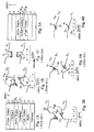
- Figure 1A is a sectional view schematically illustrating a typical conventional nitride double heterostructure semiconductor grown in a polar direction.
- the illustrated substrate layer 1 may be any material suitable for growing nitride semiconductors, including spinel (MgAl 2 O 4 ), sapphire (Al 2 O 3 ), SiC (including 6H, 4H, and 3C), ZnS, ZnO, GaAs, AlN and GaN.
- the substrate thickness typically ranges from 100 ⁇ m to 1mm.
- a buffer layer 2 on the substrate 1 can be formed of AlN, GaN, AlGaN, InGaN or the like. The buffer layer facilitates possible lattice mismatches between the substrate 1 and an overlying conductive contact layer 3.
- the buffer layer 2 may be omitted if the substrate has a lattice constant approximately equal to that of the nitride semiconductor.
- the buffer layer 2 may also be omitted with some nitride growth techniques.
- the buffer layer energy bandgap may range from 2.1eV to 6.2eV, with a thickness of about 0.5 ⁇ m to 10 ⁇ m.
- the n-type contact layer 3 is also typically formed from a nitride semiconductor, preferably GaN or InGaN with a thickness ranging from 0.5 ⁇ m to 5.0 ⁇ m, and a bandgap of approximately 3.4eV for GaN and less for InGaN (depending upon the Indium concentration).
- a lower n-type or undoped cladding layer 4 on the conductive layer 3 conventionally comprises GaN or AlGaN, with a bandgap of 3.4eV for GaN and greater for AlGaN (depending upon the Al concentration). Its thickness can range from 1nm to 100nm.
- Nitride double heterostructures typically employ InGaN as an active region 5 over the lower cladding layer, with a thickness of 1nm to 100nm.
- the bandgap of this layer is typically 2.0eV, but may vary depending upon the Indium concentration.
- a top p-type or undoped cladding layer 6 over the active region is generally comprised of AlGaN or GaN, with a thickness and bandgap energy similar to that of the lower n-type cladding layer 4.
- a p-type GaN conductive contact layer 7 on the cladding layer 6 has an energy bandgap of about 3.4eV and a thickness of about 10nm to 500nm.
- a polarization-induced sheet charge occurs at the interface between layers due to different constituent materials.
- polarization-induced charge sheets adjacent to the active region 5 are the polarization-induced charge sheets adjacent to the active region 5.
- a negative polarization-induced charge sheet density ⁇ 1 with a magnitude such as 10 13 electrons/cm 2 , is typically formed at the interface between the active region 5 and the lower cladding layer 4.
- a positive charge sheet density ⁇ 2 of similar magnitude is formed at the interface between the active region 5 and the upper cladding layer 6.
- the polarities of these charges depend upon the bonds of the crystal layers, which as mentioned above are directional and slightly ionic. In general, the density of a charge sheet will depend upon both a spontaneous factor arising from compositional differences between the two layers, and a piezoelectric strain arising from the lattice mismatch between the layers.
- ⁇ 1 between an In 0.2 Ga 0.8 N active region 5 and a GaN cladding layer 4 is about 8.3x10 12 electrons/cm 2 . This is due to the 20% Indium content in the In 0.2 Ga 0.8 N active region (spontaneous polarization), and the strain in that layer arising from the lattice mismatch with the underlying GaN layer (piezoelectric polarization).
- Interfacial charge sheets along opposite surfaces of the active region produce a dipole across the region.
- This dipole corresponds to an electric field whose strength depends on the magnitude of the sheet charges ⁇ 1 and ⁇ 2.
- a sheet charge of 8.3 ⁇ 10 12 cm -2 gives an electric field of 1.5 ⁇ 10 6 V/cm. Based on its origin, we will refer to this electric field as a polarization-induced field.
- the magnitude of the electrostatic potential drop generated by the dipole depends upon the thickness of the dipole layer.
- the thickness of the dipole layer refers to its physical dimension in the direction of growth, which is also the distance between ⁇ 1 and ⁇ 2.
- This distance can be used to determine the magnitude of the electrostatic potential drop in a manner similar to the determination of a capacitive potential drop from the distance between two capacitor plates.
- a distance of 10nm between charge densities ⁇ 1 and ⁇ 2 as given above would result in a polarization-induced potential drop of about 1.5V across the active region 5.
- the net electric field across the active region also depends on a number of parameters including the doping concentration in the surrounding cladding layers, the built in voltage across the p-n junction and free carrier screening, and is therefore not generally equal to the polarization induced field. However, due to its strength, the polarization-induced field plays a major role in determining the net electric field.
- Nitride emitters grown on a 0001 (polar) surface of a crystal have a low emission efficiency of about 1% to 10%. This can be due to the presence of significant polarization fields in or adjacent to their active regions that limit their efficiency.
- Figure 1B illustrates the energy bands corresponding to the device structure of Figure 1A .
- the naturally occurring polarization field generated by ⁇ 1 and ⁇ 2 reduces the efficiency in a number of ways.
- the dipole leads to a spatial separation (movement in the opposite direction) of electrons and holes within the region.
- carrier overshoots illustrated by carrier trajectories B, from the higher E c level on the ⁇ 1 side of the active region to the lower E c level on the ⁇ 2 side, and from the lower E v level on the ⁇ 2 side of the active region to the higher E v level on the ⁇ 1 side.
- the stability of the emission wavelength as the applied bias is increased is increased. If strong polarization-induced fields are present, the emission wavelength will blue-shift as the device bias is increased. As the device bias is increased, more free carriers accumulate in the conduction and valence band wells. Since the free carriers are spatially separated, they will themselves form a dipole that opposes, or screens, the built-in polarization induced field. As the net electric field is reduced, the quantization states of the quantum wells change, resulting in a blue-shift of the emission wavelength.
- Figure 1C illustrates the energy bands of the active layer 5 and the cladding layers 4 and 6 for a light emitter operating on a non-polar surface with no polarization-induced charges. All else being equal, its emission efficiency is higher since the three effects discussed above are either absent or greatly reduced.
- the present invention seeks to improve the operating efficiency of a compound semiconductor LED, with layers grown along a polar direction by: reducing or canceling the effect of the crystal's naturally occurring polarization-induced charges to improve carrier confinement, reducing their spatial separation, and reducing carrier overshoot.
- these charges are lowered by reducing differences in the material compositions of the crystal layers adjacent to the active region.
- the cladding layers can also be composed of a combination of elements, each of which tend to cancel the polarization effects of the others.
- One or more layers in or around the active region can also be graded in composition or doping to generate space charges that oppose the polarization-induced charges, and quasi-fields that oppose polarization-induced fields generated by the polarization-induced charges.
- the grading may be continuous or discrete.
- the compound semiconductor crystal can also have a multilayer emission system consisting of alternating light emitting and non-emitting layers to reduce the average polarization field while improving emission efficiency.
- the average field in the multilayer emission system as a whole is reduced or canceled compared to a single, uniform active region of comparable thickness.
- impurities can be incorporated into the crystal that ionize, based upon their energy levels, into a charge state opposite to polarization-induced charges to reduce or cancel their effect.
- the impurities preferably comprise group II, IV, or VI elements.
- the sign of the polarization induced charges can also be inverted to encourage, rather than oppose, the efficient confinement of carriers. These charges are inverted by inverting the atomic layer sequence of the crystal layer.
- the direction from which the carriers are injected can also be inverted, by inverting the growth order of p and n type layers, to screen polarization induced charges.
- the lattice constant of the lower buffer layer, contact layer, or cladding layer can also be changed by epitaxial growth techniques to more closely match the lattice constant of the active region. This reduces the strain-induced piezoelectric effect within the active region, reducing the polarization-induced fields for more efficient light emission.
- nitride emitter systems with a double heterostructure construction whose crystal layers are grown normal to the polar direction of the crystal.
- the nitride emitter is presumed to have the wurtzite crystal structure with layers comprising Al x In y Ga 1- x-y N, where 0 ⁇ x ⁇ 1 and 0 ⁇ y ⁇ 1. Except where noted, the top surface of the crystal is the 0001 orientation with the periodic table group III polarity.
- the nitride emitter illustrated in Figure 1A with the corresponding band structures in Figure 1B will be used as a reference for the various embodiments.
- This embodiment reduces or cancels the adverse effects of polarization-induced by incorporating various dopants into the semiconductor.
- the dopant impurity should be of a type that does not diffuse away from its intended position.
- the dopants ionize, based upon their energy levels, into either positive or negative charge states, which are opposite to the interfacial polarization-induced charge state, to cancel or reduce its effect.
- the type of dopant used depends upon the interfacial charge (positive or negative) being targeted. A positive charge would require a dopant that is ionized into a negative charge state, and the opposite for a negative interfacial charge.
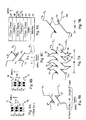
- Figure 2A illustrates the band structure of cladding/active/cladding layers incorporating approximately 10 13 Si atoms/cm 3 as a source of positive charge to reduce or cancel the negative interfacial charge density ⁇ 1.
- 10 13 atoms/ cm 3 of Mg may be used as a source of negative charge.
- the dopant concentration profile will depend in part upon the dopant ionization energy and donor/acceptor levels. For example, a higher dopant concentration would be required if Zinc (Zn) were used as a source of negative charge dopant to reduce ⁇ 2.
- the impurity profile of the dopant does not have to exactly match/cancel the polarization-induced charges to show a benefit.
- Other dopant impurities may include group II, IV, or VI elements.
- the impurity profile is preferably delta-doped at or near the plane.
- An abrupt change is one in which the change in mole fraction of a given constituent is greater than 1% over a monolayer, i.e. a single crystal layer of atoms.
- Delta doping attempts to confine the dopants to a single atomic layer, producing a dopant sheet rather than a dopant volume.
- the impurity profile is preferably also graded.
- Figure 2B illustrates various types of impurity profiles, including delta 61, graded in discrete steps 62 and continuously graded 63.
- This embodiment is directed to improving the emission efficiency of light emitters having GaN cladding layers.
- the material composition of one or both cladding layers is made intermediate with respect to the material composition of their adjacent layers to reduce or cancel both piezoelectric and spontaneous interfacial polarization-induced charges.
- Approximately 5% Indium (In) can, for example, be added to the GaN cladding layer 4 of the nitride system of Figure 1A to change the cladding layer's composition to In 0 . 05 Ga 0 . 95 N. This would make the cladding layer composition intermediate to the In 0 . 20 Ga 0 . 80 N active region 5, with 20% Indium, and GaN conductive layer 3 with 0% Indium.
- the Indium reduces differences in the material compositions of the two adjacent layers, resulting in a 25% lower interfacial polarization-induced charge sheet density ⁇ 1A of approximately 0.75x10 13 electrons/cm- between the active and cladding layers.
- ⁇ 1B is about 0.25 ⁇ 10 13 electrons/cm 2 . If donor-type doping is present near one or both of the interfaces that contain ⁇ 1A or ⁇ 1B, some of the piezo-induced charge will be screened out, as discussed in the selective doping embodiments above.
- this device structure eases the ability to selectively screen out some of the polarization-induced charges, compared with the conventional structure, while keeping dopants away from the active region. This is done by heavily n-type doping the interface with ⁇ 1B so that all of this charge is effectively screened. In this way, the electric field in the active region is reduced by as much as 25% over the conventional structure, increasing emission efficiency.
- Figure 3B illustrates the band diagram for this case. Further reduction is obtained if n-type doping extends towards interface containing 61A. The more Indium used in the cladding layer, the lower the field in the active region. However, if too much Indium is used, the carrier confinement may be compromised. The same technique can be applied to the upper cladding layer, except that p-type doping should be used for the charge screening.
- the polarization-induced electric field in the active region under device operation goes down, leading to an increase in the emission efficiency despite lower energy barriers.
- Improved LED efficiency in the 450nm to 470nm range was demonstrated using a low Indium content of about 5% in the lower cladding layer 4, compared to a cladding layer with no Indium.
- This embodiment is directed to improving the emission efficiency of light emitters having ternary AlGaN cladding layers.
- the addition of Aluminum Nitride (AlN) to the original GaN cladding layers to produce ternary AlGaN layers is known.
- This addition generates cladding layer bandgaps that are larger than the bandgaps of their adjacent contact and active layers to produce higher energy barriers on the opposite sides of the active region, thereby improving carrier confinement.
- the added Aluminum also increases variations in material composition that produce interfacial polarization-induced charges.
- both spontaneous and piezoelectric polarization-induced charges which are determined by the change in the polarity of Ga to N bonds from one layer to the next, are actually increased at the active region/cladding layer interfaces.
- the increase in charges is due to both the piezoelectric strain and spontaneous polarization differences in the two materials. As a result high electric fields exist in the active region of the device.
- One aspect of the invention reduces the strain and polarization differences by making their material compositions more similar.
- Indium Nitride (InN) is added to one or both of the ternary AlGaN cladding layers to produce a quarternary AlInGaN layer, which makes the average polarity of the bonds in both the cladding and the active layers similar.
- Indium in their layers counteracts the effect of Aluminum in generating interfacial piezoelectric polarization-induced charges at the active layer/cladding layer interfaces. That is, there is a smaller charge sheet between a quarternary AlInGaN cladding layer and an InGaN active region, than there is between a ternary AlGaN cladding layers and an InGaN active region.
- Most of the polarization-induced charge in the structure is confined to heavily doped regions within the cladding or contact layers that are removed from the active region and can be effectively screened.
- the amount of Indium added to these layers will generally depend upon the layer thickness, material composition, and growth limitations. For example, an Al 0.12 In 0.03 Ga 0.85 N cladding layer next to an In 0.05 Ga 0.95 N active layer reduces the interfacial piezoelectric charge density by approximately 30%, to 0.7x10 13 electrons/cm 2 , compared to an A1 0.15 Ga 0.85 N layer next is the same active layer, reducing the electric field in the active region by approximately 30%.
- the Indium and Aluminum components of the quaternary cladding layers tend to cancel each other's effect on the energy barriers associated with the active region. Although the addition of Indium to the AlGaN cladding layer lowers the active region's energy barriers, the confinement efficiency actually increases due to reductions in polarization-induced charges.
- the cladding layers need not have identical compositions to improve the emitter efficiency. For example, improved LED efficiency of about 25% at an emission wavelength of 380nm was demonstrated using only an upper quaternary Al 0.15 In 0.03 Ga 0.82 N cladding with energy barriers of 0.26eV E c and 0.08eV E v .
- the composition of the lower cladding layer was maintained as Al 0.15 Ga 0.85 N.
- FIG. 4A and 4B Schematic diagrams under forward bias conditions close to turn-on of an LED (i.e. close to the threshold for light emission), for cladding layers with ternary AlGaN and quarternary AlInGaN compositions, are illustrated in Figures 4A and 4B , respectively.
- the cladding layers 4 and 6 contain the same concentration of Aluminum, but with no Indium in the ternary structure.
- the slope of the line 30 in the active region 5 represents the polarization-induced field. Its strength depends upon the biasing between the contacts 3 and 7, doping in the cladding layers 4 and 6, and the magnitude of the interfacial polarization charge sheet densities.
- the biasing used for both structures is about 2.6V, with an n-type (Si) dopant concentration of approximately 1x10 18 /cm 3 in the cladding layer 4, and a p-type (Mg) dopant concentration of approximately 1x10 19 /cm3 in the cladding layer 6.
- the magnitude of the polarization induced electric field generated across the active region 5 with the ternary AlGaN cladding layers is approximately 8.8X10 5 V/cm.
- this field tends to spatially separate the electrons and the holes injected from GaN contact layers 3 and 7 by confining the carriers near interfaces 31 that are furthest away from their respective injecting contacts. This phenomenon reduces the radiative recombination probability of the carriers.
- the quarternary AlInGaN cladding layers 4 and 6 illustrated in Figure 4B exhibit a much lower polarization induced field in the active region 5.
- the field is approximately 4.6x10 5 V/cm.
- the composition of one or both of the cladding layers is graded to generate a space charge that opposes interfacial polarization effects at the interfaces between the cladding layers and the active region.
- the grading varies the layer composition in the polar direction to generate piezoelectric charges.
- the grading may be either continuous or discrete.
- the distributed charge polarity should be opposite to that of the targeted interfacial polarization charges.
- the polarity is determined by the compositions of the graded layer and its two adjacent layers. For example, the lower GaN contact layer 3 and the lower AlGaN cladding layer 4 of Figure 1A generate a positive interfacial charge sheet density.
- This charge may be distributed over the volume of the cladding layer 4 by gradually varying the Aluminum content of this layer.
- the lower cladding layer 4 may be graded from a GaN composition with 0% Aluminum near the GaN conductive layer 3, to Al 0.10 Ga 0.90 N with 10% Aluminum near the InGaN active region 5.
- the positive space charge generated would partially counter the 0.75x10 13 electrons/cm 2 negative charge sheet density ⁇ 1 at the Al 0.10 Ga 0.90 N/In 0.05 Ga 0.95 N interface.
- the negative interfacial charge density that exists between the upper GaN contact layer 7 and the upper AlGaN cladding layer 6 may be distributed over the volume of layer 6 by grading its Aluminum content.
- the negative space charge generated would counter the positive charge density ⁇ 2 to reduce or cancel its effects upon the active region.
- the magnitude of the space charge depends upon the distance over which the grade occurs.
- Figure 5 graphically illustrates the grading of the AlGaN cladding layer by the addition of Aluminum atoms (continuously 41 or discrete steps 42) to the crystal surface per unit of time, starting with 0% Aluminum.
- the added concentration of Gallium and Nitrogen atoms 40 is kept uniform throughout the growth period. The process is stopped when an appropriate cladding layer thickness and grading is achieved.
- a varying period super-lattice of two materials can also be used to make a compositional grade.
- the space charge which is generated by grading the cladding layer allows the dopant impurities to be placed outside the graded layer (e.g. in the conductive layer only), while attracting their free carriers.
- the space charge associated with the graded composition naturally attracts the free dopant carriers into the cladding layer from the adjacent conductive layer. Therefore, doping impurities need not be near the active region to provide free carriers to this region, and may be eliminated or reduced in the adjacent cladding layers.
- compositional changes in a semiconductor device on free carriers can be similar to that of an electric field, and are referred to as quasi-fields. See Herbert Kroemer, "Band Offsets and Chemical Bonding: The Basis for Heterostructure Applications", The Journal of Physica Scripta, Vol. T68, pages 10-16, 1996 .
- This embodiment of the invention uses a quasi-field to counter the effects of polarization-induced electric fields on free carriers. The establishment of a quasi-field in the active region is possible without the presence of any charges within the system.
- Figure 6A illustrates quasi-fields that are generated by gradients 51 in the energy bands, rather than from true electric charges. These gradients can be produced by grading the composition of the active region 5.
- the active region can be compositionally graded to generate a desired gradient in band structure, and thereby a desired quasi-field effect.
- the resulting quasi-field should oppose the true electric field's effect on at least one carrier type.
- the active region material composition may be graded (continuously or discretely) by varying its Indium content. Depending upon the region's width and the desired emitter properties, it may incorporate a graded composition from a low to a high Indium content or vice versa. Properties of concern typically include the emission wavelength and the operating current.
- Figures 6B and 6C illustrate the net effect of quasi-fields on the energy bands of the active region 5.
- the active region has a continuously graded Indium concentration from a low of 5% to a high of 10%, with a gradient of approximately 1%/nm.
- the Indium concentration is lowest at the interface between the cladding layer 4 and the active region 5, and increases to the highest concentration on the opposite side of the active region.
- the quasi-field reduces the polarization-induced electric field in the valence band.
- a grading in the opposite direction will offset the electric field in the conduction band.
- the active region has an Indium gradient and concentrations again from 5% to 10% and an average gradient of 1%/nm, but in the opposite direction. Since one of the carrier types, elections or holes is now spread out, there is better spatial overlap of the carriers, increasing emission efficiency.
- Figure 7A illustrates the energy bands for a multilayer emission system 90 with field-compensation energy barriers 93.
- the emissions system 90 consists of multiple layers with alternating active regions 91 (i.e. light emitting) and cladding layers 92 (non-emitting).
- the energy barriers 93 of the claddings 92 have the dual function of confining injected carriers in the active region 91, and opposing its polarization-induced fields.
- the generated field and total thickness of the multilayer emission system 90 will in general depend upon the number, thickness, and composition of the individual active regions 91 and the cladding layers 92.
- the multilayer system 90 with four In 0.1 Ga 0.9 N active regions 91 each 2nm thick and three Al 0.05 Ga 0.95 N cladding layers 92 each 5nm thick, would have a total thickness of 23nm with an approximate average polarization-induced field strength of 4.5x10 5 V/cm.
- the band structure of a single active region 100 with comparable volume, illustrated in Figure 7B could exhibit a polarization field strength of 9x10 5 V/cm.
- the use of a multilayer emission system increases the total volume of the active material while ensuring that the average field due to the polarization-induced charges in the active region as a whole is reduced compared to a structure with a single active region of comparable volume.
- the naturally occurring polarization-induced charges of a compound semiconductor are inverted to improve carrier confinement.
- the interatomic bonds in GaN are naturally ionic because the Gallium atom is slightly positive and the Nitrogen atom negative, generating a dipole across the bond.
- Figure 8A illustrates individual Gallium and Nitrogen atomic layers grown along the polar direction of the crystal surface. With the order illustrated, successive atomic layers alternate between Ga and N, with the bottom surface 70 of each layer a single atomic layer of Gallium atoms and the top surface 71 Nitrogen. The individual dipoles 72 across each GaN atomic pair add up to generate an average polarization-induced field 73 across the layer in the direction indicated. Its effect on the energy bands of the active region was described above in connection with Figure 1B .
- the direction of this naturally occurring polarization-induced field 73 can be inverted by inverting the direction of the individual atomic dipoles 72. This is accomplished by reversing the growth order of the Gallium and Nitrogen atomic layers.
- the inverted growth order of atomic layers starts with Nitrogen, and than alternates between Gallium and Nitrogen atomic layers until the top surface Ga layer 74 is reached.
- the growth order of atomic layers can be changed in several ways. First, if one starts with a N-terminated GaN or AlGaN substrate, one can grow the N-faced polarity without difficulty. However, most growth is done on sapphire or SiC and the growth naturally desires to be of the Ga-polarity. There are techniques to change the polarity.
- One technique involves using MBE growth under N-rich conditions to change the polarity.
- a second technique uses deposition of about 1 monolayer of Magnesium on the surface, which results in N-polarity growth for subsequent layers.
- a third way is to use atomic layer epitaxy by MOCVD or MBE to try to force the nucleation to be in the correct polarity.
- the individual dipoles 75 generate a polarization-induced field 76 in a reverse direction to field 73 of Fig-ure 8A . Its effect on the energy bands of the active region is illustrated in Figure 8C . Although this growth order continues to generate a polarization-induced electrical field in the active region, the field's dipole is reversed. This enables the injected carriers to screen (neutralize) the polarization-induced charge densities ⁇ 1 and ⁇ 2 before the device turn-on, i.e. before free carriers start to recombine. The electrons injected towards the active region from the cladding layer 4 above E c build up near ⁇ 2 at the cladding/active region interface. The accumulated charges of these free carriers neutralize ⁇ 2.
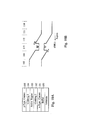
- FIG. 9A is a sectional view schematically illustrating an LED formed with the new growth sequence, with the p-type contact and cladding layers 83, 84 grown before the n-type cladding and contact layers 86 and 87.
- the thickness and material compositions of all the layers in this embodiment are similar to those for the nitride emitter described in connection with Figure 1A .
- interfacial polarization induced charge sheet densities ⁇ 1 and ⁇ 2 are still forward due to variations in material composition between layers.
- Figure 9B Their effect on the energy bands of the active region is illustrated in Figure 9B , which is essentially similar to Figure 1B .
- inverting the growth order of the p- and n-type layers has also changed the direction from which electrons and holes are injected into the active region.
- the electrons which are always injected from the n-type contact layer, are injected into the active region 85 from the contact layer 87 above E c , shown to the left of the active region 85.
- the holes are injected from the p-type contact layer 83 below E v from the right.
- This inverted layer sequence enables the carriers to screen the charge densities before the device turn-on in a manner similar to the previous embodiment, in which the field direction was inverted instead of the layer structure.
- This structure also reduces carrier overshoot and increases carrier confinement in a manner similar to the previous embodiment.
- Figures 10A and 10B illustrate another method of engineering the polarization fields in the structure.
- the piezoelectric polarization-induced fields can be reduced, eliminated, or reversed in the active region as shown in the band diagram of figure 10B .
- the underlying lattice constant can be changed in several ways.
- the buffer layer 110 can be grown with a different material composition, such as InAlGaN, so that the in-plane lattice constant of the buffer layer is close to the in-plane lattice constant of the InGaN active layer.
- the bandgap of the InAlGaN buffer layer will also be larger than that of the InGaN active layer so that there will be no light absorption.
- a second method for changing the in-plane lattice constant is to use the conventional buffer layer, but grow at least part of the n-contact layer 111 with a different material composition, such as AlInGaN, than the buffer layer so that the in-plane lattice constant is changed from that of the buffer layer to a value closer to that of the active region.
- a third method changes the lattice constant within the lower cladding layer 112 in the same way as described for the n-contact layer.
- the active region is grown thick enough to cause strain-relaxation, thus eliminating the piezoelectric-induced electric field in the active layer.
- the method chosen will generally be the one providing the least amount of material dislocations, preserving the materials quality while providing the device structure advantages described above.
Abstract
Description
- This application claims the benefit of provisional patent application Serial No.
60/168,495, filed December 2, 1999 - This invention relates to light emitting compound semiconductor crystals grown on a polar surface and, more particularly, to reduction or cancellation of their naturally occurring polarization-induced charges to improve emission efficiency.
- Most semiconductor light emitters have a double heterostructure structure that includes an active or light-generating layer grown between two cladding layers. The various layers of the double heterostructure are fabricated from more than one material. One cladding layer is n-type, which means it contains excess free electrons, and one cladding layer is p-type, which means it contains excess holes. In general, the cladding layers have larger bandgaps than the active layer. This causes injected electrons and holes to be confined within the active layer, encouraging efficient recombination of free carriers through spatial localization within the active layer to produce light. In addition, laser diode (LD) emitters also have separate light confining layers, typically comprised of a material with an even wider bandgap, surrounding a double heterostructure. Double heterostructure semiconductor devices are described in numerous publications, including O'Shea et al, Introduction to Lasers and Their Applications, Addison-Wesley Publishing Company, December 1978, pages 166-167.
- In such structures, polarization-induced charges occur when the material composition varies in a polar direction of its basic crystal structure. A polar direction is defined as any crystal direction not orthogonal to the polarization vector, P, of the crystal. This is especially true for materials whose crystal bonds are naturally directional and even slightly ionic, such as in III-V or II-VI semiconductors. These charges can be strain-related (piezoelectric) in the case of lattice mismatched materials, composition related (spontaneous) due to differences in the ionic strengths of bonds in different materials, or a combination of the two. The induced charges cause electric fields or potential gradients that have the same effect on free carriers as external fields. The phenomenon is discussed in a number of publications, including Bernardini et al, "Spontaneous polarization and piezoelectric constants of III-V nitrides," American Physical Society Journal, Physics Review B, Vol. 56, No. 16, 1997, pages R10 024 to R10 027, and Takeuchi et al, "Quantum-Confined Stark Effect due to Piezoelectric Fields in GaInN Strained Quantum Wells," Japanese Journal of Applied Physics, Vol. 36, . The magnitudes of such fields have been estimated to be as high as 2.5x10⁶ V/cm for nitride heterostructures grown on a polar surface of a crystal, Bykhovski et al., "Elastic strain relaxation and piezo-effect in GaN-AlN, Gan-AlGaN and GaN-InGaN superlattices", Journal of Applied Physics, Vol. 81, No. 9, 1997, pages 6332-6338.
- Polarization-induced charges should be taken into account when considering the electrical characteristics of heterostructures grown on crystal polar surfaces. Crystal layers grown along the 0001 orientation in the case of wurtzite GaN crystal, or along the 111 orientation in the case of zincblende GaAs crystals, are two examples of crystal polar surfaces. The Bravais lattice of the wurtzite structure is hexagonal, with the axis perpendicular to the hexagons usually labeled as the c-axis or the 0001 orientation. Along this axis the structure can be thought of as a sequence of atomic layers of the same element (e.g. all Gallium or all Nitrogen) built up from regular hexagons. Due to this uniformity, each layer (or surface) is polarized and possesses either a positive or a negative charge, generating a dipole across the atomic layers. The charge state of each layer depends upon its constituent atoms. Other examples of crystal planes with various growth directions may be found in Streetman, Solid State Electronic Devices, 2nd ed., Prentice-Hall, Inc., 1980, pages 1-24, and Shuji Nakamura et al, "The Blue Laser Diode, GaN Based Light Emitters and Lasers," Springer, 1997, pages 21-24.
- Until recently, internal polarization fields associated with the active and cladding regions of a light emitting heterostructure have not posed significant problems. This was because light emitting diodes (LEDs) based on the more established Al-Ga-In-As-P material system have typically been grown on a non-polar crystal surface (in particular the 001 zincblende surface). Recently, however, there has been considerable work in light emitters based on the A1-Ga-In-N ("nitride") materials system, mostly grown along the 0001 orientation of wurtzite crystal, which is a highly polar surface. Nevertheless, nitride double heterostructures have followed conventional non-polar designs.
-
Figure 1A is a sectional view schematically illustrating a typical conventional nitride double heterostructure semiconductor grown in a polar direction. The illustratedsubstrate layer 1 may be any material suitable for growing nitride semiconductors, including spinel (MgAl2O4), sapphire (Al2O3), SiC (including 6H, 4H, and 3C), ZnS, ZnO, GaAs, AlN and GaN. The substrate thickness typically ranges from 100µm to 1mm. Abuffer layer 2 on thesubstrate 1 can be formed of AlN, GaN, AlGaN, InGaN or the like. The buffer layer facilitates possible lattice mismatches between thesubstrate 1 and an overlyingconductive contact layer 3. However, thebuffer layer 2 may be omitted if the substrate has a lattice constant approximately equal to that of the nitride semiconductor. Thebuffer layer 2 may also be omitted with some nitride growth techniques. Depending upon the material composition, the buffer layer energy bandgap may range from 2.1eV to 6.2eV, with a thickness of about 0.5µm to 10µm. - The n-
type contact layer 3 is also typically formed from a nitride semiconductor, preferably GaN or InGaN with a thickness ranging from 0.5µm to 5.0µm, and a bandgap of approximately 3.4eV for GaN and less for InGaN (depending upon the Indium concentration). A lower n-type orundoped cladding layer 4 on theconductive layer 3 conventionally comprises GaN or AlGaN, with a bandgap of 3.4eV for GaN and greater for AlGaN (depending upon the Al concentration). Its thickness can range from 1nm to 100nm. - Nitride double heterostructures typically employ InGaN as an
active region 5 over the lower cladding layer, with a thickness of 1nm to 100nm. The bandgap of this layer is typically 2.0eV, but may vary depending upon the Indium concentration. A top p-type or undopedcladding layer 6 over the active region is generally comprised of AlGaN or GaN, with a thickness and bandgap energy similar to that of the lower n-type cladding layer 4. A p-type GaNconductive contact layer 7 on thecladding layer 6 has an energy bandgap of about 3.4eV and a thickness of about 10nm to 500nm. In general, provided the structure is grown on a polar direction such as the 0001, a polarization-induced sheet charge occurs at the interface between layers due to different constituent materials. Of particular concern for the operation of a light emitter are the polarization-induced charge sheets adjacent to theactive region 5. - With the compound semiconductor illustrated in
Figure 1A , a negative polarization-induced charge sheet density σ1, with a magnitude such as 1013 electrons/cm2, is typically formed at the interface between theactive region 5 and thelower cladding layer 4. A positive charge sheet density σ2 of similar magnitude is formed at the interface between theactive region 5 and theupper cladding layer 6. The polarities of these charges depend upon the bonds of the crystal layers, which as mentioned above are directional and slightly ionic. In general, the density of a charge sheet will depend upon both a spontaneous factor arising from compositional differences between the two layers, and a piezoelectric strain arising from the lattice mismatch between the layers. For example, σ1 between an In0.2Ga0.8Nactive region 5 and aGaN cladding layer 4 is about 8.3x10¹² electrons/cm2. This is due to the 20% Indium content in the In0.2Ga0.8N active region (spontaneous polarization), and the strain in that layer arising from the lattice mismatch with the underlying GaN layer (piezoelectric polarization). - Interfacial charge sheets along opposite surfaces of the active region produce a dipole across the region. This dipole corresponds to an electric field whose strength depends on the magnitude of the sheet charges σ1 and σ2. For the case given above, a sheet charge of 8.3×1012 cm-2 gives an electric field of 1.5×10⁶V/cm. Based on its origin, we will refer to this electric field as a polarization-induced field. The magnitude of the electrostatic potential drop generated by the dipole depends upon the thickness of the dipole layer. The thickness of the dipole layer refers to its physical dimension in the direction of growth, which is also the distance between σ1 and σ2. This distance can be used to determine the magnitude of the electrostatic potential drop in a manner similar to the determination of a capacitive potential drop from the distance between two capacitor plates. A distance of 10nm between charge densities σ1 and σ2 as given above would result in a polarization-induced potential drop of about 1.5V across the
active region 5. The net electric field across the active region also depends on a number of parameters including the doping concentration in the surrounding cladding layers, the built in voltage across the p-n junction and free carrier screening, and is therefore not generally equal to the polarization induced field. However, due to its strength, the polarization-induced field plays a major role in determining the net electric field. - Nitride emitters grown on a 0001 (polar) surface of a crystal have a low emission efficiency of about 1% to 10%. This can be due to the presence of significant polarization fields in or adjacent to their active regions that limit their efficiency.
Figure 1B illustrates the energy bands corresponding to the device structure ofFigure 1A . When the device is operating, the naturally occurring polarization field generated by σ1 and σ2 reduces the efficiency in a number of ways. First, the dipole leads to a spatial separation (movement in the opposite direction) of electrons and holes within the region. As illustrated, holes in the valence band Ev are attracted to the negative charge sheet σ1 at one end of theactive region 5, while electrons in the conduction band Ec are attracted to the positive charge sheet σ2 at its other end. This spatial separation of free carriers lowers the probability of radiative recombination, reducing emission efficiency. Second, the energy barriers of the conduction and valence band quantum wells are reduced by quantization effects associated with the electric field. Thus, carriers below Ev and above Ec escape the well through the paths indicated by dashed lines A. Third, the presence of polarization-induced fields also leads to carrier overshoots, illustrated by carrier trajectories B, from the higher Ec level on the σ1 side of the active region to the lower Ec level on the σ2 side, and from the lower Ev level on the σ2 side of the active region to the higher Ev level on the σ1 side. - Another issue of concern for applications engineers is the stability of the emission wavelength as the applied bias is increased. If strong polarization-induced fields are present, the emission wavelength will blue-shift as the device bias is increased. As the device bias is increased, more free carriers accumulate in the conduction and valence band wells. Since the free carriers are spatially separated, they will themselves form a dipole that opposes, or screens, the built-in polarization induced field. As the net electric field is reduced, the quantization states of the quantum wells change, resulting in a blue-shift of the emission wavelength.
-
Figure 1C illustrates the energy bands of theactive layer 5 and the cladding layers 4 and 6 for a light emitter operating on a non-polar surface with no polarization-induced charges. All else being equal, its emission efficiency is higher since the three effects discussed above are either absent or greatly reduced. - Several approaches to increase GaN-based LED efficiency have been used.
U.S. Patents 5,959,307 and5,578,839, both to Nakamura et al , discuss the addition of Aluminum to the cladding layers to increase the active region barrier heights for a more efficient confinement of free carriers. This addition, however, also changes the material composition of the cladding layers from GaN to AlGaN, which act to increase both spontaneous and piezoelectric polarization fields. The presence of 15% Aluminum in an Al0.15Ga0.85N cladding layer could double the polarization field in the emission layer to about 3×10⁶V/cm. Such fields may reduce carrier confinement and increase the spatial separation of carriers by changing the energy bands of the light emitter, thereby lowering its radiative efficiency. - The present invention seeks to improve the operating efficiency of a compound semiconductor LED, with layers grown along a polar direction by: reducing or canceling the effect of the crystal's naturally occurring polarization-induced charges to improve carrier confinement, reducing their spatial separation, and reducing carrier overshoot.
- In one embodiment, these charges are lowered by reducing differences in the material compositions of the crystal layers adjacent to the active region. The cladding layers can also be composed of a combination of elements, each of which tend to cancel the polarization effects of the others.
- One or more layers in or around the active region can also be graded in composition or doping to generate space charges that oppose the polarization-induced charges, and quasi-fields that oppose polarization-induced fields generated by the polarization-induced charges. The grading may be continuous or discrete.
- The compound semiconductor crystal can also have a multilayer emission system consisting of alternating light emitting and non-emitting layers to reduce the average polarization field while improving emission efficiency. The average field in the multilayer emission system as a whole is reduced or canceled compared to a single, uniform active region of comparable thickness.
- Various impurities can be incorporated into the crystal that ionize, based upon their energy levels, into a charge state opposite to polarization-induced charges to reduce or cancel their effect. The impurities preferably comprise group II, IV, or VI elements.
- The sign of the polarization induced charges can also be inverted to encourage, rather than oppose, the efficient confinement of carriers. These charges are inverted by inverting the atomic layer sequence of the crystal layer. The direction from which the carriers are injected can also be inverted, by inverting the growth order of p and n type layers, to screen polarization induced charges. The lattice constant of the lower buffer layer, contact layer, or cladding layer can also be changed by epitaxial growth techniques to more closely match the lattice constant of the active region. This reduces the strain-induced piezoelectric effect within the active region, reducing the polarization-induced fields for more efficient light emission.
- These and other features and advantages of the invention will be apparent to those skilled in the art from the following detailed description, taken together with the accompanying drawings, in which:
-
-
Figure 1A is an illustrative sectional view of a known structure for a nitride light emitter; -
Figure 1B illustrates the energy bands corresponding to the device ofFigure 1A grown on a polar surface; -
Figure 1C illustrates the energy bands of a known light emitter grown on a non-polar surface; -
Figure 2A illustrates the energy bands of the active region and cladding layers with various impurities; -
Figure 2B is a graph illustrating impurity profiles; -
Figure 3A is an illustrative sectional view of a nitride light emitter having an InGaN cladding layer in accordance with the invention; -
Figure 3B illustrates the energy bands corresponding to the device ofFigure 3A ; -
Figures 4A and 4B respectively illustrate the energy bands of a nitride semiconductor with ternary AlGaN and quarternary AlInGaN cladding layers; -
Figure 5 is a graph illustrating the relationship between the concentration of atoms as a function of time during cladding growth; -
Figure 6A illustrates the energy bands of an active region in a quasi-field; -
Figures 6B and 6C respectively illustrate the energy bands of continuously graded active regions; -
Figure 7A illustrates the energy bands of a multilayer light emission system; -
Figure 7B illustrates the energy bands of a single active region with a width equivalent to the multilayer emission system ofFigure 7A ; -
Figure 8A is a sectional view illustrating the atomic layer structure corresponding to a single layer of the structure shown inFigure 1A ; -
Figure 8B is a sectional view illustrating an inverted atomic layer structure of a single semiconductor layer; -
Figure 8C illustrates the energy bands of cladding and emission layers corresponding to the device structure ofFigure 8B ; -
Figure 9A is a sectional view illustrating an inverted nitride light emitter with p-type layers grown before n-type; -
Figure 9B illustrates the energy bands corresponding to the device ofFigure 9A ; -
Figure 10A is a sectional view illustrating a nitride light emitter with a new buffer that has a lattice constant more closely matched with the active region; and -
Figure 10B illustrates the energy bands corresponding to the device offigure 10A . - The following description of various embodiments of the present invention is directed to nitride emitter systems with a double heterostructure construction whose crystal layers are grown normal to the polar direction of the crystal. The nitride emitter is presumed to have the wurtzite crystal structure with layers comprising AlxInyGa1- x-yN, where 0≤x≤1 and 0≤y≤1. Except where noted, the top surface of the crystal is the 0001 orientation with the periodic table group III polarity. The nitride emitter illustrated in
Figure 1A with the corresponding band structures inFigure 1B will be used as a reference for the various embodiments. - This embodiment reduces or cancels the adverse effects of polarization-induced by incorporating various dopants into the semiconductor. The dopant impurity should be of a type that does not diffuse away from its intended position. The dopants ionize, based upon their energy levels, into either positive or negative charge states, which are opposite to the interfacial polarization-induced charge state, to cancel or reduce its effect. The type of dopant used depends upon the interfacial charge (positive or negative) being targeted. A positive charge would require a dopant that is ionized into a negative charge state, and the opposite for a negative interfacial charge.
-
Figure 2A illustrates the band structure of cladding/active/cladding layers incorporating approximately 1013 Si atoms/cm3 as a source of positive charge to reduce or cancel the negative interfacial charge density σ1. To reduce or cancel the positive charge density σ2, 1013 atoms/ cm3 of Mg may be used as a source of negative charge. The dopant concentration profile will depend in part upon the dopant ionization energy and donor/acceptor levels. For example, a higher dopant concentration would be required if Zinc (Zn) were used as a source of negative charge dopant to reduce σ2. The impurity profile of the dopant does not have to exactly match/cancel the polarization-induced charges to show a benefit. Other dopant impurities may include group II, IV, or VI elements. - There are several methods for distributing (or incorporating) impurities into the semiconductor. For abrupt changes in material composition, in which polarization-induced charges occur in a plane of the interface, the impurity profile is preferably delta-doped at or near the plane. An abrupt change is one in which the change in mole fraction of a given constituent is greater than 1% over a monolayer, i.e. a single crystal layer of atoms. Delta doping attempts to confine the dopants to a single atomic layer, producing a dopant sheet rather than a dopant volume. For graded composition changes, either in discrete steps or continuous, the impurity profile is preferably also graded.
Figure 2B illustrates various types of impurity profiles, includingdelta 61, graded indiscrete steps 62 and continuously graded 63. - This embodiment is directed to improving the emission efficiency of light emitters having GaN cladding layers. The material composition of one or both cladding layers is made intermediate with respect to the material composition of their adjacent layers to reduce or cancel both piezoelectric and spontaneous interfacial polarization-induced charges. Approximately 5% Indium (In) can, for example, be added to the
GaN cladding layer 4 of the nitride system ofFigure 1A to change the cladding layer's composition to In0.05Ga0.95N. This would make the cladding layer composition intermediate to the In0.20Ga0.80Nactive region 5, with 20% Indium, and GaNconductive layer 3 with 0% Indium. As illustrated inFigure 3A , the Indium reduces differences in the material compositions of the two adjacent layers, resulting in a 25% lower interfacial polarization-induced charge sheet density σ1A of approximately 0.75x10¹³ electrons/cm- between the active and cladding layers. σ1B is about 0.25×10¹³ electrons/cm2. If donor-type doping is present near one or both of the interfaces that contain σ1A or σ1B, some of the piezo-induced charge will be screened out, as discussed in the selective doping embodiments above. Since σ1A and σ1B are both smaller than the combination σ1A+σ1B, this device structure eases the ability to selectively screen out some of the polarization-induced charges, compared with the conventional structure, while keeping dopants away from the active region. This is done by heavily n-type doping the interface with σ1B so that all of this charge is effectively screened. In this way, the electric field in the active region is reduced by as much as 25% over the conventional structure, increasing emission efficiency.Figure 3B illustrates the band diagram for this case. Further reduction is obtained if n-type doping extends towards interface containing 61A. The more Indium used in the cladding layer, the lower the field in the active region. However, if too much Indium is used, the carrier confinement may be compromised. The same technique can be applied to the upper cladding layer, except that p-type doping should be used for the charge screening. - By adding Indium to one or both of the cladding layers, the polarization-induced electric field in the active region under device operation goes down, leading to an increase in the emission efficiency despite lower energy barriers. Improved LED efficiency in the 450nm to 470nm range was demonstrated using a low Indium content of about 5% in the
lower cladding layer 4, compared to a cladding layer with no Indium. - This embodiment is directed to improving the emission efficiency of light emitters having ternary AlGaN cladding layers. The addition of Aluminum Nitride (AlN) to the original GaN cladding layers to produce ternary AlGaN layers is known. This addition generates cladding layer bandgaps that are larger than the bandgaps of their adjacent contact and active layers to produce higher energy barriers on the opposite sides of the active region, thereby improving carrier confinement. However, the added Aluminum also increases variations in material composition that produce interfacial polarization-induced charges. In fact, both spontaneous and piezoelectric polarization-induced charges, which are determined by the change in the polarity of Ga to N bonds from one layer to the next, are actually increased at the active region/cladding layer interfaces. The increase in charges is due to both the piezoelectric strain and spontaneous polarization differences in the two materials. As a result high electric fields exist in the active region of the device.
- One aspect of the invention reduces the strain and polarization differences by making their material compositions more similar. Indium Nitride (InN) is added to one or both of the ternary AlGaN cladding layers to produce a quarternary AlInGaN layer, which makes the average polarity of the bonds in both the cladding and the active layers similar. The presence of Indium in their layers counteracts the effect of Aluminum in generating interfacial piezoelectric polarization-induced charges at the active layer/cladding layer interfaces. That is, there is a smaller charge sheet between a quarternary AlInGaN cladding layer and an InGaN active region, than there is between a ternary AlGaN cladding layers and an InGaN active region. Most of the polarization-induced charge in the structure is confined to heavily doped regions within the cladding or contact layers that are removed from the active region and can be effectively screened. The amount of Indium added to these layers will generally depend upon the layer thickness, material composition, and growth limitations. For example, an Al0.12In0.03Ga0.85N cladding layer next to an In0.05Ga0.95N active layer reduces the interfacial piezoelectric charge density by approximately 30%, to 0.7x10¹³electrons/cm2, compared to an A10.15Ga0.85N layer next is the same active layer, reducing the electric field in the active region by approximately 30%.
- The Indium and Aluminum components of the quaternary cladding layers tend to cancel each other's effect on the energy barriers associated with the active region. Although the addition of Indium to the AlGaN cladding layer lowers the active region's energy barriers, the confinement efficiency actually increases due to reductions in polarization-induced charges.
- The cladding layers need not have identical compositions to improve the emitter efficiency. For example, improved LED efficiency of about 25% at an emission wavelength of 380nm was demonstrated using only an upper quaternary Al0.15In0.03Ga0.82N cladding with energy barriers of 0.26eV Ec and 0.08eV Ev. The composition of the lower cladding layer was maintained as Al0.15Ga0.85N.
- Schematic diagrams under forward bias conditions close to turn-on of an LED (i.e. close to the threshold for light emission), for cladding layers with ternary AlGaN and quarternary AlInGaN compositions, are illustrated in
Figures 4A and 4B , respectively. In both structures the cladding layers 4 and 6 contain the same concentration of Aluminum, but with no Indium in the ternary structure. In both figures, the slope of theline 30 in theactive region 5 represents the polarization-induced field. Its strength depends upon the biasing between thecontacts cladding layer 4, and a p-type (Mg) dopant concentration of approximately 1x10¹⁹/cm3 in thecladding layer 6. The magnitude of the polarization induced electric field generated across theactive region 5 with the ternary AlGaN cladding layers is approximately 8.8X10⁵ V/cm. - As illustrated in
Figure 4A , this field tends to spatially separate the electrons and the holes injected from GaN contact layers 3 and 7 by confining the carriers nearinterfaces 31 that are furthest away from their respective injecting contacts. This phenomenon reduces the radiative recombination probability of the carriers. The quarternaryAlInGaN cladding layers Figure 4B exhibit a much lower polarization induced field in theactive region 5. For an Al0.05In0.025Ga0.925Nlower cladding layer 4 and an Al0.20In0.10Ga0.70Nupper cladding layer 6, the field is approximately 4.6x10⁵ V/cm. These layers also exhibitlower quantization energies 31, reducing the spatial separation of free carriers to improve radiative recombination. There is a trade-off between the reduction of polarization-induced charges and the maintenance of high energy barriers for maximum carrier confinement, which can be determined empirically. - In this embodiment, the composition of one or both of the cladding layers is graded to generate a space charge that opposes interfacial polarization effects at the interfaces between the cladding layers and the active region. The grading varies the layer composition in the polar direction to generate piezoelectric charges. The grading may be either continuous or discrete. The distributed charge polarity should be opposite to that of the targeted interfacial polarization charges. The polarity is determined by the compositions of the graded layer and its two adjacent layers. For example, the lower
GaN contact layer 3 and the lowerAlGaN cladding layer 4 ofFigure 1A generate a positive interfacial charge sheet density. This charge may be distributed over the volume of thecladding layer 4 by gradually varying the Aluminum content of this layer. In particular, thelower cladding layer 4 may be graded from a GaN composition with 0% Aluminum near the GaNconductive layer 3, to Al0.10Ga0.90N with 10% Aluminum near the InGaNactive region 5. The positive space charge generated would partially counter the 0.75x10¹³ electrons/cm2 negative charge sheet density σ1 at the Al0.10Ga0.90N/In0.05Ga0.95N interface. - The negative interfacial charge density that exists between the upper
GaN contact layer 7 and the upperAlGaN cladding layer 6 may be distributed over the volume oflayer 6 by grading its Aluminum content. The negative space charge generated would counter the positive charge density σ2 to reduce or cancel its effects upon the active region. The magnitude of the space charge depends upon the distance over which the grade occurs.Figure 5 graphically illustrates the grading of the AlGaN cladding layer by the addition of Aluminum atoms (continuously 41 or discrete steps 42) to the crystal surface per unit of time, starting with 0% Aluminum. The added concentration of Gallium andNitrogen atoms 40 is kept uniform throughout the growth period. The process is stopped when an appropriate cladding layer thickness and grading is achieved. A varying period super-lattice of two materials can also be used to make a compositional grade. - There is a trade-off between the optimal device performance due to availability of free carriers near the active region, and the adverse effects of dopant diffusion into it. The space charge which is generated by grading the cladding layer allows the dopant impurities to be placed outside the graded layer (e.g. in the conductive layer only), while attracting their free carriers. The space charge associated with the graded composition naturally attracts the free dopant carriers into the cladding layer from the adjacent conductive layer. Therefore, doping impurities need not be near the active region to provide free carriers to this region, and may be eliminated or reduced in the adjacent cladding layers.
- The effect of compositional changes in a semiconductor device on free carriers can be similar to that of an electric field, and are referred to as quasi-fields. See Herbert Kroemer, "Band Offsets and Chemical Bonding: The Basis for Heterostructure Applications", The Journal of Physica Scripta, Vol. T68, pages 10-16, 1996. This embodiment of the invention uses a quasi-field to counter the effects of polarization-induced electric fields on free carriers. The establishment of a quasi-field in the active region is possible without the presence of any charges within the system.
Figure 6A illustrates quasi-fields that are generated bygradients 51 in the energy bands, rather than from true electric charges. These gradients can be produced by grading the composition of theactive region 5. In a quasi-field, electrons in the conduction band move to a lower energy level towards the positive charge, and the holes in the valence band move to a higher energy towards the negative charge. Note that the active region band structures in this field are not parallel. By contrast, the energy bands within an electric field exhibit a parallel relationship, as illustrated inFigure 1B . The active region can be compositionally graded to generate a desired gradient in band structure, and thereby a desired quasi-field effect. The resulting quasi-field, however, should oppose the true electric field's effect on at least one carrier type. The active region material composition may be graded (continuously or discretely) by varying its Indium content. Depending upon the region's width and the desired emitter properties, it may incorporate a graded composition from a low to a high Indium content or vice versa. Properties of concern typically include the emission wavelength and the operating current. -
Figures 6B and 6C illustrate the net effect of quasi-fields on the energy bands of theactive region 5. InFigure 6B the active region has a continuously graded Indium concentration from a low of 5% to a high of 10%, with a gradient of approximately 1%/nm. The Indium concentration is lowest at the interface between thecladding layer 4 and theactive region 5, and increases to the highest concentration on the opposite side of the active region. In this case the quasi-field reduces the polarization-induced electric field in the valence band. A grading in the opposite direction will offset the electric field in the conduction band. InFigure 6C , the active region has an Indium gradient and concentrations again from 5% to 10% and an average gradient of 1%/nm, but in the opposite direction. Since one of the carrier types, elections or holes is now spread out, there is better spatial overlap of the carriers, increasing emission efficiency. -
Figure 7A illustrates the energy bands for amultilayer emission system 90 with field-compensation energy barriers 93. In this embodiment, theemissions system 90 consists of multiple layers with alternating active regions 91 (i.e. light emitting) and cladding layers 92 (non-emitting). Theenergy barriers 93 of thecladdings 92 have the dual function of confining injected carriers in theactive region 91, and opposing its polarization-induced fields. The generated field and total thickness of themultilayer emission system 90 will in general depend upon the number, thickness, and composition of the individualactive regions 91 and the cladding layers 92. Themultilayer system 90, with four In0.1Ga0.9Nactive regions 91 each 2nm thick and three Al0.05Ga0.95N cladding layers 92 each 5nm thick, would have a total thickness of 23nm with an approximate average polarization-induced field strength of 4.5x10⁵ V/cm. The band structure of a single active region 100 with comparable volume, illustrated inFigure 7B , could exhibit a polarization field strength of 9x10⁵ V/cm. The use of a multilayer emission system increases the total volume of the active material while ensuring that the average field due to the polarization-induced charges in the active region as a whole is reduced compared to a structure with a single active region of comparable volume. - In this embodiment, the naturally occurring polarization-induced charges of a compound semiconductor are inverted to improve carrier confinement. The interatomic bonds in GaN are naturally ionic because the Gallium atom is slightly positive and the Nitrogen atom negative, generating a dipole across the bond.
Figure 8A illustrates individual Gallium and Nitrogen atomic layers grown along the polar direction of the crystal surface. With the order illustrated, successive atomic layers alternate between Ga and N, with thebottom surface 70 of each layer a single atomic layer of Gallium atoms and thetop surface 71 Nitrogen. Theindividual dipoles 72 across each GaN atomic pair add up to generate an average polarization-inducedfield 73 across the layer in the direction indicated. Its effect on the energy bands of the active region was described above in connection withFigure 1B . - The direction of this naturally occurring polarization-induced
field 73 can be inverted by inverting the direction of the individualatomic dipoles 72. This is accomplished by reversing the growth order of the Gallium and Nitrogen atomic layers. InFigure 8B , the inverted growth order of atomic layers starts with Nitrogen, and than alternates between Gallium and Nitrogen atomic layers until the topsurface Ga layer 74 is reached. The growth order of atomic layers can be changed in several ways. First, if one starts with a N-terminated GaN or AlGaN substrate, one can grow the N-faced polarity without difficulty. However, most growth is done on sapphire or SiC and the growth naturally desires to be of the Ga-polarity. There are techniques to change the polarity. One technique involves using MBE growth under N-rich conditions to change the polarity. A second technique uses deposition of about 1 monolayer of Magnesium on the surface, which results in N-polarity growth for subsequent layers. A third way is to use atomic layer epitaxy by MOCVD or MBE to try to force the nucleation to be in the correct polarity. - The individual dipoles 75 generate a polarization-induced
field 76 in a reverse direction to field 73 ofFig-ure 8A . Its effect on the energy bands of the active region is illustrated inFigure 8C . Although this growth order continues to generate a polarization-induced electrical field in the active region, the field's dipole is reversed. This enables the injected carriers to screen (neutralize) the polarization-induced charge densities σ1 and σ2 before the device turn-on, i.e. before free carriers start to recombine. The electrons injected towards the active region from thecladding layer 4 above Ec build up near σ2 at the cladding/active region interface. The accumulated charges of these free carriers neutralize σ2. Similarly, the holes injected from thecladding layer 6 below Ev neutralize σ1 near the active region/cladding interface. Before device turn-on, this process "flattens" the active region energy bands, similar to those illustrated inFigure 1C . Consequently, the efficiency of the device is not reduced by the polarization-induced charges. A further benefit of this device structure is that the carrier overshoots denoted as paths A are dramatically reduced compared to the conventional structure. Also, the carrier confinement of both electrons and holes is increased. - In a conventional LED, the n-type layers are grown before the p-type. This embodiment inverts this growth sequence.
Figure 9A is a sectional view schematically illustrating an LED formed with the new growth sequence, with the p-type contact and cladding layers 83, 84 grown before the n-type cladding andcontact layers Figure 1A . Despite an inverted layer structure, interfacial polarization induced charge sheet densities σ1 and σ2 are still forward due to variations in material composition between layers. Their effect on the energy bands of the active region is illustrated inFigure 9B , which is essentially similar toFigure 1B . However, inverting the growth order of the p- and n-type layers has also changed the direction from which electrons and holes are injected into the active region. In this way the electrons, which are always injected from the n-type contact layer, are injected into theactive region 85 from thecontact layer 87 above Ec, shown to the left of theactive region 85. The holes are injected from the p-type contact layer 83 below Ev from the right. This inverted layer sequence enables the carriers to screen the charge densities before the device turn-on in a manner similar to the previous embodiment, in which the field direction was inverted instead of the layer structure. This structure also reduces carrier overshoot and increases carrier confinement in a manner similar to the previous embodiment. -
Figures 10A and 10B illustrate another method of engineering the polarization fields in the structure. By changing the in-plane lattice constant of the structure beneath theactive region 113 so that the active layer is under less strain, or the strain direction is reversed, the piezoelectric polarization-induced fields can be reduced, eliminated, or reversed in the active region as shown in the band diagram offigure 10B . The underlying lattice constant can be changed in several ways. First, thebuffer layer 110 can be grown with a different material composition, such as InAlGaN, so that the in-plane lattice constant of the buffer layer is close to the in-plane lattice constant of the InGaN active layer. The bandgap of the InAlGaN buffer layer will also be larger than that of the InGaN active layer so that there will be no light absorption. A second method for changing the in-plane lattice constant is to use the conventional buffer layer, but grow at least part of the n-contact layer 111 with a different material composition, such as AlInGaN, than the buffer layer so that the in-plane lattice constant is changed from that of the buffer layer to a value closer to that of the active region. Thus, the same benefits as described above are realized. A third method changes the lattice constant within thelower cladding layer 112 in the same way as described for the n-contact layer. In a fourth method, the active region is grown thick enough to cause strain-relaxation, thus eliminating the piezoelectric-induced electric field in the active layer. The method chosen will generally be the one providing the least amount of material dislocations, preserving the materials quality while providing the device structure advantages described above. - There are a number of ways to further reduce or cancel most of the residual polarization-induced charges. The various embodiments discussed above could be mixed-and-matched and applied to any one or all appropriate layers, emitting or non-emitting. For any given application, the particular embodiment or combination of embodiments would depend upon the nature of the application, and can be determined empirically. For example, one possibility would be to combine AlGaN cladding layers 92 and InGaN
active regions 91 with the counteracting effects of Aluminum and Indium mentioned in connection with quarternary barriers. Another would be to grade the Aluminum content of at least onecladding layer 92 and/or to add impurities that ionize into a charged state opposing the interfacial polarization-induced charges. - While several illustrative embodiments of the invention have been shown and described, numerous variations and alternate embodiments will occur to those skilled in the art. For example, although the description was directed to nitride emitters, any or all of the embodiments may be used to address the problems of polarization-induced charges in light emitters comprised of other materials. Such variations and alternate embodiments are contemplated, and can be made without departing from the spirit and scope of the invention as defined in the appended claims.
- Preferred embodiments of the invention are as follows:
- 1. An optical emitter, comprising:
- a high efficiency double heterostructure with n-type and p-type contact layers (3,7), and cladding layers (4,6) sandwiching an active light emitting region (5) and grown along a crystal polar direction,
- said high efficiency heterostructure having a structural difference from a base heterostructure which comprises an active region (5) with atomic dipoles which generate a polarization-induced electric field across the active region (5), and binary or ternary cladding layers (4,6) with said n-type contact layer (3) preceding said p-type contact layer (7) in growth order,
- said structural difference at least partially alleviating the efficiency reducing effects of a polarization-induced electric field across the active region (5) of said high efficiency heterostructure compared to the polarization-induced electric field of said base heterostructure.
- 2. The optical emitter of
embodiment 1, said active region (5) comprising InGaN and said structural difference comprising the addition of In to at least one of said cladding layers (4,6) such that at least one of said cladding layers (4,6) comprises AlxInyGa1-x-yN, where 0≤x≤1 and 0≤y≤1. - 3. The optical emitter of
embodiment 1, wherein said structural difference comprises a gradient in the composition of at least one of said cladding layers (4,6) to oppose interfacial polarization effects at the interfaces between at least one of said cladding layers (4,6) and the active region (5). - 4. The optical emitter of
embodiment 1, wherein said structural difference comprises a gradient in the composition of said active region (5) to oppose said polarization-induced field. - 5. The optical emitter of
embodiment 1, said structural difference comprising the addition of dopant impurities in at least one of said cladding layers (4,6) which reduce said polarization-induced field. - 6. The optical emitter of
embodiment 1, said structural difference comprising an inversion of said active region atomic dipoles (72). - 7. The optical emitter of
embodiment 1, said structural difference comprising said p-type contact layer (83) preceding said n-type contact layer (87) in growth order. - 8. The optical emitter of
embodiment 1, said structural difference comprising multiple active regions (91) alternating with cladding layers (92). - 9. The optical emitter of
embodiment 1, said structural difference comprising an at least partially strain-relaxed lower cladding layer (112) having an in-plane lattice constant close in value to the in-plane lattice constant of unstrained active region material (113) . - 10. The optical emitter of
embodiment 1, said structural difference comprising an at least partially strain-relaxed n-type contact layer (111) having an in-plane lattice constant close in value to the in-plane lattice constant of unstrained active region material (113). - 11. The optical emitter of
embodiment 1, grown on a buffer layer (110), said structural difference comprising said buffer layer (110) being at least partially strain-relaxed and having an in-plane lattice constant close in value to the in-plane lattice constant of unstrained active region material (113). - 12. A compound semiconductor device grown normal to a crystal polar direction, comprising:
- at least three crystal layers (2-7) whose material compositions vary in said polar direction;
- at least one of said layers (2-7) having an intermediate material composition relative to the material compositions of two adjacent layers.
- 13. The device of embodiment 12, wherein said at least one layer (2-7) is an AlxInyGa1-x-yN cladding layer, where 0≤x≤1 and 0≤y≤1.
- 14. A compound semiconductor device grown normal to a crystal polar direction, comprising:
- a plurality of crystal layers (2-7) whose material compositions vary in said polar direction to generate at least one polarization-induced charge concentration in at least one of said layers (2-7);
- at least one of said layers (2-7) comprising a cladding layer (4,6) whose composition is graded to generate a space charge over a volume of said grade that opposes said charge concentration.
- 15. The device of embodiment 14, wherein said graded cladding layer (4,6) comprises AlxlnyGa1-x-yN, where 0≤x≤1 and 0≤y≤1.
- 16. A compound semiconductor device grown along a crystal polar direction, comprising:
- a plurality of crystal layers (2-7) whose material compositions vary in said polar direction;
- at least one of said layers (4,6) having its composition graded to generate a space charge over a volume of said grade that allows dopant impurities to be set back from an adjacent layer.
- 17. The device of embodiment 16, wherein said graded layer comprises AlxInyGa1-x-yN, where 0≤x≤1 and 0≤y≤1.
- 18. A compound semiconductor device grown along a crystal polar direction, comprising:
- a plurality of crystal layers (2-7) whose material compositions vary in said polar direction to generate a polarization-induced electric field in at least one of said layers;
- one of said layers comprising an active region (5) whose composition is graded to generate a quasi-field that opposes said polarization-induced electric field.
- 19. The device of embodiment 18, wherein said grading generates gradients in the energy bands of said active region (5) to produce said quasi-field.
- 20. The device of embodiment 18, wherein said active region (5) is comprised of InyAlxGa1-x-yN, where 0≤y≤1 and 0≤x≤1.
- 21. A compound semiconductor device grown along a crystal polar direction, comprising:
- a plurality of crystal layers (2-7) whose material compositions vary in said polar direction to generate a polarization-induced charge concentration in at least one of said layers;
- at least one of said layers (2-7) incorporating dopant impurities that ionize into a charged state opposite to at least one of said charge concentrations.
- 22. A compound semiconductor device, comprising:
- a crystal having a polar direction; and
- a plurality of crystal layers (2-7) whose material compositions vary in said crystal polar direction to generate a polarization-induced electric field in at least one of said layers,
- at least one of said layers (2-7) having a polarity alternating atomic layer sequence that reverses the direction of said polarization-induced electric field in at least one of said layers.
- 23. A compound semiconductor device, comprising:
- a crystal having a polar direction; and
- at least one each of p-type (83,84) and n-type crystal layers (86,87) whose material compositions vary in said polar direction to generate a polarization-induced charge concentration in at least one of said layers;
- said p-type layers (83,84) preceding said n-type layers (86,87) in growth sequence to reverse the effect of said charge concentration on said device's performance.
- 24. A compound semiconductor device grown normal to a crystal polar direction, comprising:
- a plurality of crystal layers whose material compositions vary in said polar direction to generate a polarization-induced electric fields in at least one of said layers;
- one of said layers comprising a multilayer active region that comprises alternating optical emitting and non-emitting layers (91,92), with said non-emitting layers (92) confining injected carriers in said emitting layers (91) and opposing said electric fields.
- 25. The device of embodiment 24, wherein the material composition of at least one of said non-emitting layers (92) is graded to create a quasi-field opposing said electric fields.
- 26. The device of embodiment 24, wherein the material composition of at least one of said emitting layers (91) is graded to create a quasi-field opposing said electric fields.
- 27. The device of embodiment 26, wherein the material composition of at least one of said non-emitting layers (92) is graded to create a quasi-field opposing said electric fields.
- 28. The device of embodiment 24, wherein at least one of said non-emitting layers (92) includes dopant impurities to provide space charge that will oppose said electric fields.
- 29. A compound semiconductor device, comprising:
- a crystal having a polar direction; and
- a plurality of crystal layers (2-7) whose material compositions vary in said polar direction to generate polarization-induced electric fields in at least one of said layers;
- at least one of said layers (2-7) being an active region (5);
- one of said layers (2-4), below said active region (5), being at least partially strain-relaxed such that the in-plane lattice constant of said layer below the active region (5) is close to the unstrained in-plane lattice constant of said active region (5), thus reducing, eliminating, or reversing said electric field in said active region (5).
- 30. A compound semiconductor device, comprising:
- a crystal having a polar direction; and
- a plurality of crystal layers (2-7) whose material compositions vary in said polar direction to generate polarization-induced electric fields in at least one of said layers;
- at least one of said layers (2-7) being an active region (5);
- said active region (5) grown so that material in said device is at least partially strain-relaxed, thereby reducing said electric field in at least said active region (5).
Claims (5)
- A device which is selected from:(i) a compound semiconductor device, comprising:a crystal having a polar direction; anda plurality of crystal layers (2-7) whose material compositions vary in said crystal polar direction to generate a polarization-induced electric field in at least one of said layers,at least one of said layers (2-7) having a polarity alternating atomic layer sequence that reverses the direction of said polarization-induced electric field in at least one of said layers;(ii) a compound semiconductor device grown normal to a crystal polar direction, comprising:a plurality of crystal layers whose material compositions vary in said polar direction to generate a polarization-induced electric field in at least one of said layers;one of said layers comprising a multilayer active region that comprises alternating optical emitting and nonemitting layers (91,92), with said non-emitting layers (92) confining injected carriers in said emitting layers (91) and opposing said electric fields;and(iii) an optical emitter, comprising:a high efficiency double heterostructure with n-type and p-type contact layers (3,7),and cladding layers (4,6) sandwiching an active light emitting region (5) and grown along a crystal polar direction,said high efficiency heterostructure having a structural difference from a base heterostructure which comprises an active region (5) with atomic dipoles which generate a polarization-induced electric field across the active region (5), and binary or ternary cladding layers (4,6) with said n-type contact layer (3) preceding said p-type contact layer (7) in growth order, said structural difference further comprising multiple active regions (91) alternating with cladding layers (92); andsaid structural difference at least partially alleviating the efficiency reducing effects of a polarization-induced electric field across the active region (5) of said high efficiency heterostructure compared to the polarization-induced electric field of said base heterostructure.
- The device of claim 1, wherein said device is a compound semiconductor device, comprising:a crystal having a polar direction; anda plurality of crystal layers (2-7) whose material compositions vary in said crystal polar direction to generate a polarization-induced electric field in at least one of said layers,at least one of said layers (2-7) having a polarity alternating atomic layer sequence that reverses the direction of said polarization-induced electric field in at least one of said layers.
- The device of claim 2, further comprising active regions alternating with cladding layers.
- The device of claim 1, wherein said device is a compound semiconductor device grown normal to a crystal polar direction, comprising:a plurality of crystal layers whose material compositions vary in said polar direction to generate a polarization-induced electric field in at least one of said layers;one of said layers comprising a multilayer active region that comprises alternating optical emitting and nonemitting layers (91,92), with said non-emitting layers (92) confining injected carriers in said emitting layers (91) and opposing said electric fields.
- The device of claim 1, wherein said device is an optical emitter, comprising:a high efficiency double heterostructure with n-type and p-type contact layers (3,7),and cladding layers (4,6) sandwiching an active light emitting region (5) and grown along a crystal polar direction,said high efficiency heterostructure having a structural difference from a base heterostructure which comprises an active region (5) with atomic dipoles which generate a polarization-induced electric field across the active region (5), and binary or ternary cladding layers (4,6) with said n-type contact layer (3) preceding said ptype contact layer (7) in growth order, said structural difference further comprising multiple active regions (91) alternating with cladding layers (92); andsaid structural difference at least partially alleviating the efficiency reducing effects of a polarization-induced electric field across the active region (5) of said high efficiency heterostructure compared to the polarization-induced electric field of said base heterostructure.
Applications Claiming Priority (3)
| Application Number | Priority Date | Filing Date | Title |
|---|---|---|---|
| US16849599P | 1999-12-02 | 1999-12-02 | |
| US09/728,788 US6515313B1 (en) | 1999-12-02 | 2000-11-28 | High efficiency light emitters with reduced polarization-induced charges |
| EP00980912A EP1266411A2 (en) | 1999-12-02 | 2000-11-30 | High efficiency light emitters with reduced polarization-induced charges |
Related Parent Applications (1)
| Application Number | Title | Priority Date | Filing Date |
|---|---|---|---|
| EP00980912.0 Division | 2000-11-30 |
Publications (1)
| Publication Number | Publication Date |
|---|---|
| EP2362436A1 true EP2362436A1 (en) | 2011-08-31 |
Family
ID=26864178
Family Applications (8)
| Application Number | Title | Priority Date | Filing Date |
|---|---|---|---|
| EP10196041.7A Expired - Lifetime EP2362437B1 (en) | 1999-12-02 | 2000-11-30 | High efficiency light emitters with reduced polarization-induced charges |
| EP10196040A Withdrawn EP2362436A1 (en) | 1999-12-02 | 2000-11-30 | High efficiency light emitters with reduced polarization-induced charges |
| EP00980912A Ceased EP1266411A2 (en) | 1999-12-02 | 2000-11-30 | High efficiency light emitters with reduced polarization-induced charges |
| EP10196038A Withdrawn EP2362435A1 (en) | 1999-12-02 | 2000-11-30 | High efficiency light emitters with reduced polarization-induced charges |
| EP10196036A Ceased EP2362434A1 (en) | 1999-12-02 | 2000-11-30 | High efficiency light emitters with reduced polarization-induced charges |
| EP10196031A Ceased EP2362433A1 (en) | 1999-12-02 | 2000-11-30 | High efficiency light emitters with reduced polarization-induced charges |
| EP10196056A Withdrawn EP2365537A1 (en) | 1999-12-02 | 2000-11-30 | High efficiency light emitters with reduced polarization-induced charges |
| EP10196055A Withdrawn EP2365536A1 (en) | 1999-12-02 | 2000-11-30 | High efficiency light emitters with reduced polarization-induced charges |
Family Applications Before (1)
| Application Number | Title | Priority Date | Filing Date |
|---|---|---|---|
| EP10196041.7A Expired - Lifetime EP2362437B1 (en) | 1999-12-02 | 2000-11-30 | High efficiency light emitters with reduced polarization-induced charges |
Family Applications After (6)
| Application Number | Title | Priority Date | Filing Date |
|---|---|---|---|
| EP00980912A Ceased EP1266411A2 (en) | 1999-12-02 | 2000-11-30 | High efficiency light emitters with reduced polarization-induced charges |
| EP10196038A Withdrawn EP2362435A1 (en) | 1999-12-02 | 2000-11-30 | High efficiency light emitters with reduced polarization-induced charges |
| EP10196036A Ceased EP2362434A1 (en) | 1999-12-02 | 2000-11-30 | High efficiency light emitters with reduced polarization-induced charges |
| EP10196031A Ceased EP2362433A1 (en) | 1999-12-02 | 2000-11-30 | High efficiency light emitters with reduced polarization-induced charges |
| EP10196056A Withdrawn EP2365537A1 (en) | 1999-12-02 | 2000-11-30 | High efficiency light emitters with reduced polarization-induced charges |
| EP10196055A Withdrawn EP2365536A1 (en) | 1999-12-02 | 2000-11-30 | High efficiency light emitters with reduced polarization-induced charges |
Country Status (9)
| Country | Link |
|---|---|
| US (1) | US6515313B1 (en) |
| EP (8) | EP2362437B1 (en) |
| JP (2) | JP2003527745A (en) |
| KR (1) | KR100704588B1 (en) |
| CN (2) | CN1433579A (en) |
| AU (1) | AU1811001A (en) |
| CA (1) | CA2393044C (en) |
| MY (1) | MY123546A (en) |
| WO (1) | WO2001041224A2 (en) |
Families Citing this family (144)
| Publication number | Priority date | Publication date | Assignee | Title |
|---|---|---|---|---|
| US6849472B2 (en) | 1997-09-30 | 2005-02-01 | Lumileds Lighting U.S., Llc | Nitride semiconductor device with reduced polarization fields |
| JP3955367B2 (en) | 1997-09-30 | 2007-08-08 | フィリップス ルミレッズ ライティング カンパニー リミテッド ライアビリティ カンパニー | Optical semiconductor device and manufacturing method thereof |
| US6853663B2 (en) * | 2000-06-02 | 2005-02-08 | Agilent Technologies, Inc. | Efficiency GaN-based light emitting devices |
| DE50112334D1 (en) * | 2000-06-02 | 2007-05-24 | Microgan Gmbh | HETEROSTRUCTURE WITH BACK DONATE ORDERING |
| JP3864735B2 (en) * | 2000-12-28 | 2007-01-10 | ソニー株式会社 | Semiconductor light emitting device and manufacturing method thereof |
| US6800876B2 (en) * | 2001-01-16 | 2004-10-05 | Cree, Inc. | Group III nitride LED with undoped cladding layer (5000.137) |
| USRE46589E1 (en) * | 2001-01-16 | 2017-10-24 | Cree, Inc. | Group III nitride LED with undoped cladding layer and multiple quantum well |
| GB2372632A (en) * | 2001-02-23 | 2002-08-28 | Sharp Kk | A method of growing an InGaN semiconductor layer |
| JP2002289955A (en) * | 2001-03-23 | 2002-10-04 | Sharp Corp | Semiconductor laser element, manufacturing method therefor and optical information reproducing device |
| US6955933B2 (en) * | 2001-07-24 | 2005-10-18 | Lumileds Lighting U.S., Llc | Light emitting diodes with graded composition active regions |
| JP2003229645A (en) * | 2002-01-31 | 2003-08-15 | Nec Corp | Quantum well structure, semiconductor element employing it and its fabricating method |
| US8809867B2 (en) * | 2002-04-15 | 2014-08-19 | The Regents Of The University Of California | Dislocation reduction in non-polar III-nitride thin films |
| US7091514B2 (en) * | 2002-04-15 | 2006-08-15 | The Regents Of The University Of California | Non-polar (Al,B,In,Ga)N quantum well and heterostructure materials and devices |
| JP2005056973A (en) * | 2003-08-01 | 2005-03-03 | Hitachi Cable Ltd | Semiconductor light emitting device and epitaxial wafer therefor for manufacturing the same |
| JP4958288B2 (en) * | 2003-08-20 | 2012-06-20 | 住友電気工業株式会社 | Method for manufacturing light emitting device |
| JP4110222B2 (en) * | 2003-08-20 | 2008-07-02 | 住友電気工業株式会社 | Light emitting diode |
| JP2008109166A (en) * | 2003-08-20 | 2008-05-08 | Sumitomo Electric Ind Ltd | Light-emitting device and manufacturing method therefor |
| TWI233697B (en) * | 2003-08-28 | 2005-06-01 | Genesis Photonics Inc | AlInGaN light-emitting diode with wide spectrum and solid-state white light device |
| US20050077538A1 (en) * | 2003-10-10 | 2005-04-14 | The Regents Of The University Of California | Design methodology for multiple channel heterostructures in polar materials |
| JP2005203520A (en) * | 2004-01-14 | 2005-07-28 | Sumitomo Electric Ind Ltd | Semiconductor light emitting element |
| US6943381B2 (en) * | 2004-01-30 | 2005-09-13 | Lumileds Lighting U.S., Llc | III-nitride light-emitting devices with improved high-current efficiency |
| US7115908B2 (en) * | 2004-01-30 | 2006-10-03 | Philips Lumileds Lighting Company, Llc | III-nitride light emitting device with reduced polarization fields |
| US7285799B2 (en) * | 2004-04-21 | 2007-10-23 | Philip Lumileds Lighting Company, Llc | Semiconductor light emitting devices including in-plane light emitting layers |
| KR100513923B1 (en) * | 2004-08-13 | 2005-09-08 | 재단법인서울대학교산학협력재단 | Growth method of nitride semiconductor layer and light emitting device using the growth method |
| FI20041213A0 (en) * | 2004-09-17 | 2004-09-17 | Optogan Oy | Parts Half heterostructure |
| AU2005322570A1 (en) * | 2004-10-08 | 2006-07-06 | The Regents Of The University Of California | High efficiency light-emitting diodes |
| US7122839B2 (en) * | 2004-10-29 | 2006-10-17 | Philips Lumileds Lighting Company, Llc | Semiconductor light emitting devices with graded composition light emitting layers |
| US7221000B2 (en) | 2005-02-18 | 2007-05-22 | Philips Lumileds Lighting Company, Llc | Reverse polarization light emitting region for a semiconductor light emitting device |
| US7804100B2 (en) * | 2005-03-14 | 2010-09-28 | Philips Lumileds Lighting Company, Llc | Polarization-reversed III-nitride light emitting device |
| US7417258B2 (en) * | 2005-04-28 | 2008-08-26 | Sharp Kabushiki Kaisha | Semiconductor light-emitting device, and a method of manufacture of a semiconductor device |
| JP2006324279A (en) * | 2005-05-17 | 2006-11-30 | Rohm Co Ltd | Semiconductor element |
| US7391058B2 (en) * | 2005-06-27 | 2008-06-24 | General Electric Company | Semiconductor devices and methods of making same |
| DE102005035722B9 (en) * | 2005-07-29 | 2021-11-18 | OSRAM Opto Semiconductors Gesellschaft mit beschränkter Haftung | Optoelectronic semiconductor chip and method for its production |
| US20070045638A1 (en) * | 2005-08-24 | 2007-03-01 | Lumileds Lighting U.S., Llc | III-nitride light emitting device with double heterostructure light emitting region |
| JP2007080896A (en) * | 2005-09-12 | 2007-03-29 | Sanyo Electric Co Ltd | Semiconductor element |
| JP2007081180A (en) * | 2005-09-15 | 2007-03-29 | Matsushita Electric Ind Co Ltd | Semiconductor light-emitting element |
| EP1974389A4 (en) | 2006-01-05 | 2010-12-29 | Illumitex Inc | Separate optical device for directing light from an led |
| US8124957B2 (en) | 2006-02-22 | 2012-02-28 | Cree, Inc. | Low resistance tunnel junctions in wide band gap materials and method of making same |
| US7737451B2 (en) * | 2006-02-23 | 2010-06-15 | Cree, Inc. | High efficiency LED with tunnel junction layer |
| JP2007305965A (en) * | 2006-04-14 | 2007-11-22 | Toyoda Gosei Co Ltd | Light-emitting element, and communication device using the same |
| US9335006B2 (en) * | 2006-04-18 | 2016-05-10 | Cree, Inc. | Saturated yellow phosphor converted LED and blue converted red LED |
| JP4884826B2 (en) * | 2006-04-28 | 2012-02-29 | ローム株式会社 | Semiconductor light emitting device |
| RU2306634C1 (en) | 2006-08-08 | 2007-09-20 | Закрытое Акционерное Общество "Светлана - Оптоэлектроника" | Light-emitting semiconductor heterostructure |
| US20090275266A1 (en) * | 2006-10-02 | 2009-11-05 | Illumitex, Inc. | Optical device polishing |
| JP2010506402A (en) * | 2006-10-02 | 2010-02-25 | イルミテックス, インコーポレイテッド | LED system and method |
| US7781247B2 (en) * | 2006-10-26 | 2010-08-24 | SemiLEDs Optoelectronics Co., Ltd. | Method for producing Group III-Group V vertical light-emitting diodes |
| US7834367B2 (en) | 2007-01-19 | 2010-11-16 | Cree, Inc. | Low voltage diode with reduced parasitic resistance and method for fabricating |
| US20080258135A1 (en) * | 2007-04-19 | 2008-10-23 | Hoke William E | Semiconductor structure having plural back-barrier layers for improved carrier confinement |
| KR100929307B1 (en) | 2007-06-11 | 2009-11-27 | 고려대학교 산학협력단 | Vertical light emitting device and manufacturing method |
| DE102007031926A1 (en) * | 2007-07-09 | 2009-01-15 | Osram Opto Semiconductors Gmbh | Radiation-emitting semiconductor body |
| KR101012514B1 (en) * | 2007-08-20 | 2011-02-08 | 렌슬러 폴리테크닉 인스티튜트 | Nitride semiconductor light emitting device |
| US8519437B2 (en) * | 2007-09-14 | 2013-08-27 | Cree, Inc. | Polarization doping in nitride based diodes |
| US9012937B2 (en) | 2007-10-10 | 2015-04-21 | Cree, Inc. | Multiple conversion material light emitting diode package and method of fabricating same |
| KR100961108B1 (en) | 2007-11-27 | 2010-06-07 | 삼성엘이디 주식회사 | Nitride semiconductor light emitting device with reduced polarization effect |
| US7928448B2 (en) * | 2007-12-04 | 2011-04-19 | Philips Lumileds Lighting Company, Llc | III-nitride light emitting device including porous semiconductor layer |
| EP2198494B1 (en) * | 2007-12-28 | 2019-10-02 | Avago Technologies International Sales Pte. Limited | Waveguide device having delta doped active region |
| KR101459763B1 (en) * | 2008-01-15 | 2014-11-12 | 엘지이노텍 주식회사 | Semiconductor light emitting device and fabrication method thereof |
| JP2011511462A (en) * | 2008-02-01 | 2011-04-07 | ザ リージェンツ オブ ザ ユニバーシティ オブ カリフォルニア | Enhanced polarization of nitride light-emitting diodes by off-axis wafer cutting |
| JP2011511463A (en) * | 2008-02-01 | 2011-04-07 | ザ リージェンツ オブ ザ ユニバーシティ オブ カリフォルニア | Increased polarization of nitride light-emitting diodes due to increased indium incorporation |
| EP2240968A1 (en) * | 2008-02-08 | 2010-10-20 | Illumitex, Inc. | System and method for emitter layer shaping |
| US8278679B2 (en) * | 2008-04-29 | 2012-10-02 | Tsmc Solid State Lighting Ltd. | LED device with embedded top electrode |
| US7956369B2 (en) | 2008-05-07 | 2011-06-07 | The United States Of America As Represented By The Secretary Of The Army | Light emitting diode |
| JP2010040692A (en) * | 2008-08-04 | 2010-02-18 | Furukawa Electric Co Ltd:The | Nitride based semiconductor device and method of manufacturing the same |
| US8000366B2 (en) * | 2008-11-21 | 2011-08-16 | Palo Alto Research Center Incorporated | Laser diode with high indium active layer and lattice matched cladding layer |
| TW201034256A (en) * | 2008-12-11 | 2010-09-16 | Illumitex Inc | Systems and methods for packaging light-emitting diode devices |
| US8373153B2 (en) * | 2009-05-26 | 2013-02-12 | University Of Seoul Industry Cooperation Foundation | Photodetectors |
| CN102460739A (en) * | 2009-06-05 | 2012-05-16 | 加利福尼亚大学董事会 | Long wavelength nonpolar and semipolar (al,ga,in)n based laser diodes |
| US8367925B2 (en) * | 2009-06-29 | 2013-02-05 | University Of Seoul Industry Cooperation Foundation | Light-electricity conversion device |
| US8395141B2 (en) * | 2009-07-06 | 2013-03-12 | University Of Seoul Industry Cooperation Foundation | Compound semiconductors |
| US8227793B2 (en) * | 2009-07-06 | 2012-07-24 | University Of Seoul Industry Cooperation Foundation | Photodetector capable of detecting the visible light spectrum |
| US8809834B2 (en) * | 2009-07-06 | 2014-08-19 | University Of Seoul Industry Cooperation Foundation | Photodetector capable of detecting long wavelength radiation |
| US8748862B2 (en) * | 2009-07-06 | 2014-06-10 | University Of Seoul Industry Cooperation Foundation | Compound semiconductors |
| US8585253B2 (en) | 2009-08-20 | 2013-11-19 | Illumitex, Inc. | System and method for color mixing lens array |
| US8449128B2 (en) * | 2009-08-20 | 2013-05-28 | Illumitex, Inc. | System and method for a lens and phosphor layer |
| US8368990B2 (en) | 2009-08-21 | 2013-02-05 | University Of Seoul Industry Cooperation Foundation | Polariton mode optical switch with composite structure |
| US8368047B2 (en) * | 2009-10-27 | 2013-02-05 | University Of Seoul Industry Cooperation Foundation | Semiconductor device |
| US8058641B2 (en) * | 2009-11-18 | 2011-11-15 | University of Seoul Industry Corporation Foundation | Copper blend I-VII compound semiconductor light-emitting devices |
| US8907321B2 (en) * | 2009-12-16 | 2014-12-09 | Lehigh Univeristy | Nitride based quantum well light-emitting devices having improved current injection efficiency |
| US8536615B1 (en) | 2009-12-16 | 2013-09-17 | Cree, Inc. | Semiconductor device structures with modulated and delta doping and related methods |
| US8604461B2 (en) | 2009-12-16 | 2013-12-10 | Cree, Inc. | Semiconductor device structures with modulated doping and related methods |
| DE102010012711A1 (en) | 2010-03-25 | 2011-09-29 | Osram Opto Semiconductors Gmbh | A radiation-emitting semiconductor component and method for producing a radiation-emitting semiconductor component |
| US10134948B2 (en) * | 2011-02-25 | 2018-11-20 | Sensor Electronic Technology, Inc. | Light emitting diode with polarization control |
| US8409892B2 (en) * | 2011-04-14 | 2013-04-02 | Opto Tech Corporation | Method of selective photo-enhanced wet oxidation for nitride layer regrowth on substrates |
| WO2013009552A2 (en) * | 2011-07-08 | 2013-01-17 | RoseStreet Labs Energy, LLC | Multi-color light emitting devices with compositionally graded cladding group iii-nitride layers grown on substrates |
| JP5238865B2 (en) * | 2011-10-11 | 2013-07-17 | 株式会社東芝 | Semiconductor light emitting device |
| JP5629714B2 (en) * | 2012-03-19 | 2014-11-26 | トヨタ自動車株式会社 | Semiconductor device |
| US9029830B2 (en) | 2012-05-07 | 2015-05-12 | Sharp Kabushiki Kaisha | Multi-quantum well LED structure with varied barrier layer composition |
| US9401452B2 (en) | 2012-09-14 | 2016-07-26 | Palo Alto Research Center Incorporated | P-side layers for short wavelength light emitters |
| US9219189B2 (en) * | 2012-09-14 | 2015-12-22 | Palo Alto Research Center Incorporated | Graded electron blocking layer |
| US8814376B2 (en) | 2012-09-26 | 2014-08-26 | Apogee Translite, Inc. | Lighting devices |
| US20140154826A1 (en) * | 2012-11-30 | 2014-06-05 | Palo Alto Research Center Incorporated | Etch stop layers in nitride semiconductors created by polarity inversion |
| CN102961394A (en) * | 2012-12-10 | 2013-03-13 | 厦门大学 | Application of geniposide in preparation of medicine for treating fatty liver disease |
| US8882298B2 (en) | 2012-12-14 | 2014-11-11 | Remphos Technologies Llc | LED module for light distribution |
| US9182091B2 (en) | 2012-12-14 | 2015-11-10 | Remphos Technologies Llc | LED panel light fixture |
| DE102013104192A1 (en) * | 2013-04-25 | 2014-10-30 | Osram Opto Semiconductors Gmbh | Semiconductor device with an intermediate layer |
| CN103247728B (en) * | 2013-05-09 | 2016-01-13 | 青岛杰生电气有限公司 | A kind of semiconductive ultraviolet light source device |
| US9964266B2 (en) | 2013-07-05 | 2018-05-08 | DMF, Inc. | Unified driver and light source assembly for recessed lighting |
| US11435064B1 (en) | 2013-07-05 | 2022-09-06 | DMF, Inc. | Integrated lighting module |
| US10563850B2 (en) | 2015-04-22 | 2020-02-18 | DMF, Inc. | Outer casing for a recessed lighting fixture |
| US10139059B2 (en) | 2014-02-18 | 2018-11-27 | DMF, Inc. | Adjustable compact recessed lighting assembly with hangar bars |
| US10753558B2 (en) | 2013-07-05 | 2020-08-25 | DMF, Inc. | Lighting apparatus and methods |
| US11060705B1 (en) | 2013-07-05 | 2021-07-13 | DMF, Inc. | Compact lighting apparatus with AC to DC converter and integrated electrical connector |
| US11255497B2 (en) | 2013-07-05 | 2022-02-22 | DMF, Inc. | Adjustable electrical apparatus with hangar bars for installation in a building |
| US10551044B2 (en) | 2015-11-16 | 2020-02-04 | DMF, Inc. | Recessed lighting assembly |
| DK2824147T3 (en) | 2013-07-12 | 2016-04-18 | Omya Int Ag | Use of 2-amino-2-ethyl-1,3-propanediol as an additive in aqueous suspensions of calcium carbonate comprising materials while maintaining stable suspension conductivity |
| KR101533619B1 (en) * | 2013-10-28 | 2015-07-03 | 정선호 | Methods for designing and manufacturing devices that force atoms to emit spectrums |
| CN106415854B (en) | 2014-05-27 | 2019-10-01 | 斯兰纳Uv科技有限公司 | Electronic device including N-type and p-type superlattices |
| JP6817072B2 (en) | 2014-05-27 | 2021-01-20 | シランナ・ユー・ブイ・テクノロジーズ・プライベート・リミテッドSilanna Uv Technologies Pte Ltd | Optoelectronic device |
| US11322643B2 (en) | 2014-05-27 | 2022-05-03 | Silanna UV Technologies Pte Ltd | Optoelectronic device |
| CN106537617B (en) | 2014-05-27 | 2019-04-16 | 斯兰纳Uv科技有限公司 | Use the advanced electronics structure of semiconductor structure and superlattices |
| US10797204B2 (en) | 2014-05-30 | 2020-10-06 | Cree, Inc. | Submount based light emitter components and methods |
| DE102014111058A1 (en) | 2014-08-04 | 2016-02-04 | Osram Opto Semiconductors Gmbh | Optoelectronic component and method for the production |
| US9985168B1 (en) | 2014-11-18 | 2018-05-29 | Cree, Inc. | Group III nitride based LED structures including multiple quantum wells with barrier-well unit interface layers |
| CZ201582A3 (en) * | 2015-02-09 | 2016-06-29 | Crytur, Spol.S R.O. | Scintillation detector for detecting ionizing radiation |
| US20180076354A1 (en) * | 2015-03-27 | 2018-03-15 | Ohio State Innovation Foundation | Ultraviolet light emitting diodes with tunnel junction |
| JP6785221B2 (en) * | 2015-03-30 | 2020-11-18 | パナソニック株式会社 | Semiconductor light emitting device |
| WO2016176625A1 (en) | 2015-04-30 | 2016-11-03 | Cree, Inc. | Solid state lighting components |
| CA2931588C (en) | 2015-05-29 | 2021-09-14 | DMF, Inc. | Lighting module for recessed lighting systems |
| USD851046S1 (en) | 2015-10-05 | 2019-06-11 | DMF, Inc. | Electrical Junction Box |
| KR101936086B1 (en) * | 2016-03-21 | 2019-04-03 | 정선호 | Designing and Manufacturing Devices that Emit Desired Spectrums |
| CN106098882B (en) * | 2016-07-25 | 2020-08-18 | 华灿光电(浙江)有限公司 | Light emitting diode epitaxial wafer and preparation method thereof |
| CN106129209B (en) * | 2016-08-23 | 2019-01-22 | 扬州中科半导体照明有限公司 | A kind of epitaxial wafer and its growing method of high LED luminous efficiency |
| US11211525B2 (en) | 2017-05-01 | 2021-12-28 | Ohio State Innovation Foundation | Tunnel junction ultraviolet light emitting diodes with enhanced light extraction efficiency |
| WO2018237294A2 (en) | 2017-06-22 | 2018-12-27 | DMF, Inc. | Thin profile surface mount lighting apparatus |
| USD905327S1 (en) | 2018-05-17 | 2020-12-15 | DMF, Inc. | Light fixture |
| US10488000B2 (en) | 2017-06-22 | 2019-11-26 | DMF, Inc. | Thin profile surface mount lighting apparatus |
| US11067231B2 (en) | 2017-08-28 | 2021-07-20 | DMF, Inc. | Alternate junction box and arrangement for lighting apparatus |
| DE102017119931A1 (en) * | 2017-08-30 | 2019-02-28 | Osram Opto Semiconductors Gmbh | Optoelectronic semiconductor component |
| DE102018112472A1 (en) * | 2017-10-17 | 2019-04-18 | easE-Link GmbH | Ground contact unit for a vehicle battery charging system and method for switching a contact area of a ground contact unit |
| CA3083359A1 (en) | 2017-11-28 | 2019-06-06 | DMF, Inc. | Adjustable hanger bar assembly |
| CA3087187A1 (en) | 2017-12-27 | 2019-07-04 | DMF, Inc. | Methods and apparatus for adjusting a luminaire |
| USD877957S1 (en) | 2018-05-24 | 2020-03-10 | DMF Inc. | Light fixture |
| CA3103255A1 (en) | 2018-06-11 | 2019-12-19 | DMF, Inc. | A polymer housing for a recessed lighting system and methods for using same |
| USD903605S1 (en) | 2018-06-12 | 2020-12-01 | DMF, Inc. | Plastic deep electrical junction box |
| US11393948B2 (en) | 2018-08-31 | 2022-07-19 | Creeled, Inc. | Group III nitride LED structures with improved electrical performance |
| CA3115146A1 (en) | 2018-10-02 | 2020-04-09 | Ver Lighting Llc | A bar hanger assembly with mating telescoping bars |
| USD901398S1 (en) | 2019-01-29 | 2020-11-10 | DMF, Inc. | Plastic deep electrical junction box |
| USD1012864S1 (en) | 2019-01-29 | 2024-01-30 | DMF, Inc. | Portion of a plastic deep electrical junction box |
| USD864877S1 (en) | 2019-01-29 | 2019-10-29 | DMF, Inc. | Plastic deep electrical junction box with a lighting module mounting yoke |
| USD966877S1 (en) | 2019-03-14 | 2022-10-18 | Ver Lighting Llc | Hanger bar for a hanger bar assembly |
| CA3154491A1 (en) | 2019-09-12 | 2021-03-18 | DMF, Inc. | Miniature lighting module and lighting fixtures using same |
| USD990030S1 (en) | 2020-07-17 | 2023-06-20 | DMF, Inc. | Housing for a lighting system |
| CA3124976A1 (en) | 2020-07-17 | 2022-01-17 | DMF, Inc. | Polymer housing for a lighting system and methods for using same |
| CA3125954A1 (en) | 2020-07-23 | 2022-01-23 | DMF, Inc. | Lighting module having field-replaceable optics, improved cooling, and tool-less mounting features |
Citations (7)
| Publication number | Priority date | Publication date | Assignee | Title |
|---|---|---|---|---|
| US5075743A (en) * | 1989-06-06 | 1991-12-24 | Cornell Research Foundation, Inc. | Quantum well optical device on silicon |
| US5432808A (en) * | 1993-03-15 | 1995-07-11 | Kabushiki Kaisha Toshiba | Compound semicondutor light-emitting device |
| JPH08255932A (en) * | 1995-01-19 | 1996-10-01 | Matsushita Electric Ind Co Ltd | Semiconductor light emission element and fabrication thereof |
| US5578839A (en) | 1992-11-20 | 1996-11-26 | Nichia Chemical Industries, Ltd. | Light-emitting gallium nitride-based compound semiconductor device |
| US5851905A (en) * | 1996-07-11 | 1998-12-22 | North Carolina State University | Methods of forming indium gallium nitride or aluminum indium gallium nitride using controlled hydrogen gas flows |
| US5909040A (en) * | 1994-03-09 | 1999-06-01 | Kabushiki Kaisha Toshiba | Semiconductor device including quaternary buffer layer with pinholes |
| US5959307A (en) | 1995-11-06 | 1999-09-28 | Nichia Chemical Industries Ltd. | Nitride semiconductor device |
Family Cites Families (45)
| Publication number | Priority date | Publication date | Assignee | Title |
|---|---|---|---|---|
| US4301616A (en) | 1979-11-19 | 1981-11-24 | Gudgel Terry J | Illuminated frisbee toy |
| US5165065A (en) | 1985-04-19 | 1992-11-17 | Texas Instruments Incorporated | Optically pumped quantum coupled devices |
| JPS622684A (en) * | 1985-06-28 | 1987-01-08 | Nec Corp | Semiconductor laser |
| US4725128A (en) | 1985-11-20 | 1988-02-16 | Medtronic, Inc. | Method for delivering light from multiple light emitting diodes over a single optical fiber |
| JPH0677598A (en) * | 1992-08-25 | 1994-03-18 | Mitsubishi Electric Corp | Semiconductor laser and manufacture thereof |
| JP3207618B2 (en) * | 1993-06-25 | 2001-09-10 | 株式会社東芝 | Semiconductor device |
| JP3243111B2 (en) * | 1993-03-15 | 2002-01-07 | 株式会社東芝 | Compound semiconductor device |
| EP0952617B1 (en) * | 1993-04-28 | 2004-07-28 | Nichia Corporation | Gallium nitride-based III-V group compound semiconductor device |
| JPH07235732A (en) * | 1993-12-28 | 1995-09-05 | Nec Corp | Semiconductor laser |
| JP3325380B2 (en) * | 1994-03-09 | 2002-09-17 | 株式会社東芝 | Semiconductor light emitting device and method of manufacturing the same |
| US5689123A (en) * | 1994-04-07 | 1997-11-18 | Sdl, Inc. | III-V aresenide-nitride semiconductor materials and devices |
| US5448082A (en) * | 1994-09-27 | 1995-09-05 | Opto Diode Corporation | Light emitting diode for use as an efficient emitter or detector of light at a common wavelength and method for forming the same |
| JP3657795B2 (en) * | 1995-02-23 | 2005-06-08 | 日亜化学工業株式会社 | Light emitting element |
| EP0732754B1 (en) * | 1995-03-17 | 2007-10-31 | Toyoda Gosei Co., Ltd. | Light-emitting semiconductor device using group III nitride compound |
| US5679965A (en) * | 1995-03-29 | 1997-10-21 | North Carolina State University | Integrated heterostructures of Group III-V nitride semiconductor materials including epitaxial ohmic contact, non-nitride buffer layer and methods of fabricating same |
| US5670798A (en) * | 1995-03-29 | 1997-09-23 | North Carolina State University | Integrated heterostructures of Group III-V nitride semiconductor materials including epitaxial ohmic contact non-nitride buffer layer and methods of fabricating same |
| JP2839077B2 (en) | 1995-06-15 | 1998-12-16 | 日本電気株式会社 | Gallium nitride based compound semiconductor light emitting device |
| JPH0951143A (en) * | 1995-08-07 | 1997-02-18 | Mitsubishi Electric Corp | Manufacture of semiconductor device and manufacture of semiconductor laser |
| US5798537A (en) * | 1995-08-31 | 1998-08-25 | Kabushiki Kaisha Toshiba | Blue light-emitting device |
| JPH09139543A (en) * | 1995-11-15 | 1997-05-27 | Hitachi Ltd | Semiconductor laser element |
| US5780867A (en) * | 1996-03-07 | 1998-07-14 | Sandia Corporation | Broadband light-emitting diode |
| US5727012A (en) * | 1996-03-07 | 1998-03-10 | Lucent Technologies Inc. | Heterostructure laser |
| DE19613265C1 (en) * | 1996-04-02 | 1997-04-17 | Siemens Ag | Circuit element, e.g. laser diode |
| US5694412A (en) | 1996-04-08 | 1997-12-02 | He Holdings Inc. | Epitaxial visible-light-emitting devices with light extracted through the substrate and method of making same |
| US5813148A (en) | 1996-04-08 | 1998-09-29 | Guerra; Rafael J. | Footwear with optical fiber illuminating display areas and control module |
| US5834331A (en) * | 1996-10-17 | 1998-11-10 | Northwestern University | Method for making III-Nitride laser and detection device |
| JP3282175B2 (en) * | 1997-02-04 | 2002-05-13 | 日亜化学工業株式会社 | Nitride semiconductor device |
| JP3713118B2 (en) * | 1997-03-04 | 2005-11-02 | ローム株式会社 | Manufacturing method of semiconductor light emitting device |
| JPH10247747A (en) * | 1997-03-05 | 1998-09-14 | Toshiba Corp | Semiconductor light emitting device and manufacture thereof |
| AU7566298A (en) * | 1997-05-14 | 1998-12-08 | Research Triangle Institute | Light emitting device contact layers having substantially equal spreading resistance and method of manufacture |
| JP3955367B2 (en) * | 1997-09-30 | 2007-08-08 | フィリップス ルミレッズ ライティング カンパニー リミテッド ライアビリティ カンパニー | Optical semiconductor device and manufacturing method thereof |
| JP3180743B2 (en) * | 1997-11-17 | 2001-06-25 | 日本電気株式会社 | Nitride compound semiconductor light emitting device and method of manufacturing the same |
| JP3468082B2 (en) * | 1998-02-26 | 2003-11-17 | 日亜化学工業株式会社 | Nitride semiconductor device |
| JP3369464B2 (en) * | 1998-03-19 | 2003-01-20 | 日本電信電話株式会社 | Semiconductor device |
| JP4186306B2 (en) * | 1998-05-06 | 2008-11-26 | 松下電器産業株式会社 | Semiconductor device |
| JPH11330553A (en) * | 1998-05-15 | 1999-11-30 | Sanyo Electric Co Ltd | Semiconductor element and its manufacture |
| JPH11330552A (en) * | 1998-05-18 | 1999-11-30 | Nichia Chem Ind Ltd | Nitride semiconductor light-emitting element and light-emitting device |
| JPH11340559A (en) * | 1998-05-22 | 1999-12-10 | Hitachi Ltd | Semiconductor light-emitting element |
| JP2000261106A (en) * | 1999-01-07 | 2000-09-22 | Matsushita Electric Ind Co Ltd | Semiconductor light emitting element, its manufacture and optical disk device |
| JP3678399B2 (en) * | 1999-01-29 | 2005-08-03 | 株式会社東芝 | Nitride semiconductor laser device |
| JP2000244069A (en) * | 1999-02-18 | 2000-09-08 | Nippon Telegr & Teleph Corp <Ntt> | Semiconductor hetero structure |
| JP2000277868A (en) * | 1999-03-25 | 2000-10-06 | Sanyo Electric Co Ltd | Light emitting element |
| JP3763701B2 (en) * | 1999-05-17 | 2006-04-05 | 株式会社東芝 | Gallium nitride semiconductor light emitting device |
| JP3438648B2 (en) * | 1999-05-17 | 2003-08-18 | 松下電器産業株式会社 | Nitride semiconductor device |
| DE19955747A1 (en) * | 1999-11-19 | 2001-05-23 | Osram Opto Semiconductors Gmbh | Optical semiconductor device with multiple quantum well structure, e.g. LED, has alternate well layers and barrier layers forming super-lattices |
-
2000
- 2000-11-28 US US09/728,788 patent/US6515313B1/en not_active Expired - Lifetime
- 2000-11-30 EP EP10196041.7A patent/EP2362437B1/en not_active Expired - Lifetime
- 2000-11-30 EP EP10196040A patent/EP2362436A1/en not_active Withdrawn
- 2000-11-30 EP EP00980912A patent/EP1266411A2/en not_active Ceased
- 2000-11-30 WO PCT/US2000/032712 patent/WO2001041224A2/en active Application Filing
- 2000-11-30 EP EP10196038A patent/EP2362435A1/en not_active Withdrawn
- 2000-11-30 CN CN00818793A patent/CN1433579A/en active Pending
- 2000-11-30 CN CN2009102049844A patent/CN101692477B/en not_active Expired - Lifetime
- 2000-11-30 AU AU18110/01A patent/AU1811001A/en not_active Abandoned
- 2000-11-30 EP EP10196036A patent/EP2362434A1/en not_active Ceased
- 2000-11-30 EP EP10196031A patent/EP2362433A1/en not_active Ceased
- 2000-11-30 CA CA2393044A patent/CA2393044C/en not_active Expired - Lifetime
- 2000-11-30 EP EP10196056A patent/EP2365537A1/en not_active Withdrawn
- 2000-11-30 KR KR1020027007121A patent/KR100704588B1/en active IP Right Grant
- 2000-11-30 EP EP10196055A patent/EP2365536A1/en not_active Withdrawn
- 2000-11-30 JP JP2001542396A patent/JP2003527745A/en active Pending
- 2000-12-01 MY MYPI20005640A patent/MY123546A/en unknown
-
2012
- 2012-10-01 JP JP2012219430A patent/JP5852945B2/en not_active Expired - Lifetime
Patent Citations (7)
| Publication number | Priority date | Publication date | Assignee | Title |
|---|---|---|---|---|
| US5075743A (en) * | 1989-06-06 | 1991-12-24 | Cornell Research Foundation, Inc. | Quantum well optical device on silicon |
| US5578839A (en) | 1992-11-20 | 1996-11-26 | Nichia Chemical Industries, Ltd. | Light-emitting gallium nitride-based compound semiconductor device |
| US5432808A (en) * | 1993-03-15 | 1995-07-11 | Kabushiki Kaisha Toshiba | Compound semicondutor light-emitting device |
| US5909040A (en) * | 1994-03-09 | 1999-06-01 | Kabushiki Kaisha Toshiba | Semiconductor device including quaternary buffer layer with pinholes |
| JPH08255932A (en) * | 1995-01-19 | 1996-10-01 | Matsushita Electric Ind Co Ltd | Semiconductor light emission element and fabrication thereof |
| US5959307A (en) | 1995-11-06 | 1999-09-28 | Nichia Chemical Industries Ltd. | Nitride semiconductor device |
| US5851905A (en) * | 1996-07-11 | 1998-12-22 | North Carolina State University | Methods of forming indium gallium nitride or aluminum indium gallium nitride using controlled hydrogen gas flows |
Non-Patent Citations (8)
| Title |
|---|
| BERNARDINI ET AL.: "Journal, Physics Review B", vol. 56, 1997, AMERICAN PHYSICAL SOCIETY, article "Spontaneous polarization and piezoelectric constants of III-V nitrides", pages: R10 024 - RIO 027 |
| BYKHOVSKI ET AL.: "Elastic strain relaxation and piezo-effect in GaN-AlN, Gan-AlGaN and GaN-InGaN superlat- tices", JOURNAL OF APPLIED PHYSICS, vol. 81, no. 9, 1997, pages 6332 - 6338 |
| HER- BERT KROEMER: "The Journal of Physica", vol. 68, 1996, SCRIPTA, article "Band Offsets and Chemical Bonding: The Basis for Heterostructure Applications", pages: 10 - 16 |
| O'SHEA ET AL.: "Introduction to Lasers and Their Applications", December 1978, ADDISON-WESLEY PUBLISHING COMPANY, pages: 166 - 167 |
| ROUVIERE J L ET AL: "Polarity determination for GaN films grown on (0001) sapphire and high-pressure-grown GaN single crystals", APPLIED PHYSICS LETTERS, AIP, AMERICAN INSTITUTE OF PHYSICS, MELVILLE, NY, US, vol. 73, no. 5, 3 August 1998 (1998-08-03), pages 668 - 670, XP012021876, ISSN: 0003-6951, DOI: 10.1063/1.121942 * |
| SHUJI NAKAMURA ET AL.: "The Blue Laser Diode, GaN Based Light Emitters and Lasers", 1997, SPRINGER, pages: 21 - 24 |
| STREETMAN: "Solid State Electronic Devices", 1980, PRENTICE-HALL, INC., pages: 1 - 24 |
| TAKEUCHI ET AL.: "Quantum-Confined Stark Effect due to Piezoelectric Fields in GaInN Strained Quantum Wells", JAPANESE JOURNAL OF APPLIED PHYSICS, vol. 36, no. 4, 1997, pages 382 - L385 |
Also Published As
| Publication number | Publication date |
|---|---|
| JP2003527745A (en) | 2003-09-16 |
| EP2362433A1 (en) | 2011-08-31 |
| CA2393044C (en) | 2012-01-03 |
| JP2012256952A (en) | 2012-12-27 |
| EP2362437B1 (en) | 2019-08-28 |
| JP5852945B2 (en) | 2016-02-03 |
| EP2362435A1 (en) | 2011-08-31 |
| CN1433579A (en) | 2003-07-30 |
| AU1811001A (en) | 2001-06-12 |
| EP2362434A1 (en) | 2011-08-31 |
| CN101692477B (en) | 2013-09-18 |
| EP1266411A2 (en) | 2002-12-18 |
| KR100704588B1 (en) | 2007-04-10 |
| WO2001041224A2 (en) | 2001-06-07 |
| US6515313B1 (en) | 2003-02-04 |
| WO2001041224A3 (en) | 2002-01-17 |
| KR20020068365A (en) | 2002-08-27 |
| CA2393044A1 (en) | 2001-06-07 |
| CN101692477A (en) | 2010-04-07 |
| EP2365536A1 (en) | 2011-09-14 |
| EP2365537A1 (en) | 2011-09-14 |
| EP2362437A1 (en) | 2011-08-31 |
| MY123546A (en) | 2006-05-31 |
Similar Documents
| Publication | Publication Date | Title |
|---|---|---|
| EP2362437B1 (en) | High efficiency light emitters with reduced polarization-induced charges | |
| KR100735934B1 (en) | Semiconductor devices with selectively doped ?-? nitride layers | |
| KR101466674B1 (en) | Radiation-emitting semiconductor body | |
| EP1560277B1 (en) | III-Nitride light-emitting devices with improved high-current efficiency | |
| KR100267839B1 (en) | Nitride semiconductor device | |
| US6995389B2 (en) | Heterostructures for III-nitride light emitting devices | |
| US6337493B1 (en) | Nitride semiconductor device | |
| US8124957B2 (en) | Low resistance tunnel junctions in wide band gap materials and method of making same | |
| US20160149075A1 (en) | Optoelectronic Device | |
| US6198112B1 (en) | III-V compound semiconductor luminescent device | |
| EP1653522A2 (en) | Semiconductor light emitting devices with graded composition light emitting layers | |
| WO2015181657A1 (en) | Advanced electronic device structures using semiconductor structures and superlattices | |
| EP1992050A1 (en) | High efficiency leds with tunnel junctions | |
| US20240097066A1 (en) | Semiconductor structure with superlattices | |
| JP2008066555A (en) | Semiconductor device and method of manufacturing semiconductor device | |
| TW497276B (en) | High efficiency light emitters with reduced polarization-induced charges |
Legal Events
| Date | Code | Title | Description |
|---|---|---|---|
| PUAI | Public reference made under article 153(3) epc to a published international application that has entered the european phase |
Free format text: ORIGINAL CODE: 0009012 |
|
| AC | Divisional application: reference to earlier application |
Ref document number: 1266411 Country of ref document: EP Kind code of ref document: P |
|
| AK | Designated contracting states |
Kind code of ref document: A1 Designated state(s): AT BE CH CY DE DK ES FI FR GB GR IE IT LI LU MC NL PT SE TR |
|
| 17P | Request for examination filed |
Effective date: 20120229 |
|
| 17Q | First examination report despatched |
Effective date: 20150825 |
|
| STAA | Information on the status of an ep patent application or granted ep patent |
Free format text: STATUS: THE APPLICATION IS DEEMED TO BE WITHDRAWN |
|
| 18D | Application deemed to be withdrawn |
Effective date: 20190424 |