EP2416319A2 - Systems and methods for sequence detection in data processing - Google Patents
Systems and methods for sequence detection in data processing Download PDFInfo
- Publication number
- EP2416319A2 EP2416319A2 EP20110275074 EP11275074A EP2416319A2 EP 2416319 A2 EP2416319 A2 EP 2416319A2 EP 20110275074 EP20110275074 EP 20110275074 EP 11275074 A EP11275074 A EP 11275074A EP 2416319 A2 EP2416319 A2 EP 2416319A2
- Authority
- EP
- European Patent Office
- Prior art keywords
- value
- state
- interim
- yield
- surviving
- Prior art date
- Legal status (The legal status is an assumption and is not a legal conclusion. Google has not performed a legal analysis and makes no representation as to the accuracy of the status listed.)
- Granted
Links
Images


Classifications
-
- G—PHYSICS
- G11—INFORMATION STORAGE
- G11B—INFORMATION STORAGE BASED ON RELATIVE MOVEMENT BETWEEN RECORD CARRIER AND TRANSDUCER
- G11B20/00—Signal processing not specific to the method of recording or reproducing; Circuits therefor
- G11B20/10—Digital recording or reproducing
- G11B20/10009—Improvement or modification of read or write signals
-
- G—PHYSICS
- G11—INFORMATION STORAGE
- G11B—INFORMATION STORAGE BASED ON RELATIVE MOVEMENT BETWEEN RECORD CARRIER AND TRANSDUCER
- G11B20/00—Signal processing not specific to the method of recording or reproducing; Circuits therefor
- G11B20/10—Digital recording or reproducing
-
- G—PHYSICS
- G11—INFORMATION STORAGE
- G11B—INFORMATION STORAGE BASED ON RELATIVE MOVEMENT BETWEEN RECORD CARRIER AND TRANSDUCER
- G11B20/00—Signal processing not specific to the method of recording or reproducing; Circuits therefor
- G11B20/10—Digital recording or reproducing
- G11B20/10009—Improvement or modification of read or write signals
- G11B20/10046—Improvement or modification of read or write signals filtering or equalising, e.g. setting the tap weights of an FIR filter
- G11B20/10055—Improvement or modification of read or write signals filtering or equalising, e.g. setting the tap weights of an FIR filter using partial response filtering when writing the signal to the medium or reading it therefrom
-
- G—PHYSICS
- G11—INFORMATION STORAGE
- G11B—INFORMATION STORAGE BASED ON RELATIVE MOVEMENT BETWEEN RECORD CARRIER AND TRANSDUCER
- G11B20/00—Signal processing not specific to the method of recording or reproducing; Circuits therefor
- G11B20/10—Digital recording or reproducing
- G11B20/10009—Improvement or modification of read or write signals
- G11B20/10268—Improvement or modification of read or write signals bit detection or demodulation methods
- G11B20/10277—Improvement or modification of read or write signals bit detection or demodulation methods the demodulation process being specifically adapted to partial response channels, e.g. PRML decoding
-
- G—PHYSICS
- G11—INFORMATION STORAGE
- G11B—INFORMATION STORAGE BASED ON RELATIVE MOVEMENT BETWEEN RECORD CARRIER AND TRANSDUCER
- G11B20/00—Signal processing not specific to the method of recording or reproducing; Circuits therefor
- G11B20/10—Digital recording or reproducing
- G11B20/10009—Improvement or modification of read or write signals
- G11B20/10268—Improvement or modification of read or write signals bit detection or demodulation methods
- G11B20/10287—Improvement or modification of read or write signals bit detection or demodulation methods using probabilistic methods, e.g. maximum likelihood detectors
- G11B20/10296—Improvement or modification of read or write signals bit detection or demodulation methods using probabilistic methods, e.g. maximum likelihood detectors using the Viterbi algorithm
-
- H—ELECTRICITY
- H04—ELECTRIC COMMUNICATION TECHNIQUE
- H04L—TRANSMISSION OF DIGITAL INFORMATION, e.g. TELEGRAPHIC COMMUNICATION
- H04L25/00—Baseband systems
- H04L25/02—Details ; arrangements for supplying electrical power along data transmission lines
- H04L25/03—Shaping networks in transmitter or receiver, e.g. adaptive shaping networks
- H04L25/03006—Arrangements for removing intersymbol interference
- H04L25/03178—Arrangements involving sequence estimation techniques
- H04L25/03184—Details concerning the metric
-
- H—ELECTRICITY
- H03—ELECTRONIC CIRCUITRY
- H03M—CODING; DECODING; CODE CONVERSION IN GENERAL
- H03M13/00—Coding, decoding or code conversion, for error detection or error correction; Coding theory basic assumptions; Coding bounds; Error probability evaluation methods; Channel models; Simulation or testing of codes
- H03M13/37—Decoding methods or techniques, not specific to the particular type of coding provided for in groups H03M13/03 - H03M13/35
- H03M13/39—Sequence estimation, i.e. using statistical methods for the reconstruction of the original codes
- H03M13/41—Sequence estimation, i.e. using statistical methods for the reconstruction of the original codes using the Viterbi algorithm or Viterbi processors
- H03M13/4161—Sequence estimation, i.e. using statistical methods for the reconstruction of the original codes using the Viterbi algorithm or Viterbi processors implementing path management
Definitions
- the present inventions are related to systems and methods for processing data, and more particularly to systems and methods for detecting data sequences.
- a typical data processing system receives an analog input signal that is sampled to yield a series of digital samples.
- the data often includes sequences of data used for data synchronization and/or other purposes.
- Various existing data processing systems utilize, for example, a Viterbi sequence detection circuit. Such a circuit operates well where the received digital samples of the analog input signal are accurately equalized to a target response and accurate timing and gain control are applied. In some cases, sufficient accuracy is hard to achieve resulting in degraded performance of the sequence detection.
- Other approaches rely on threshold detection processes that work reasonably well in low noise environments, but as channel bit densities increase the effects of noise increase rendering such threshold approaches less effective.
- the present inventions are related to systems and methods for processing data, and more particularly to systems and methods for detecting data sequences.
- a method for data detection includes receiving a series of data samples at a detector circuit; multiplying a portion of the series of data samples by a first correlator value corresponding to a first binary transition to yield a first value; multiplying the portion of the series of data samples by a second correlator value corresponding to a second binary transition to yield a second value; adding the first value to a prior state value to yield a first interim value; adding the second value to the prior state value to yield a second interim value; and selecting the larger of the first interim value and the second interim value to yield a surviving interim value.
- the method may further include storing the surviving interim value as the prior state value.
- the surviving interim value may be a first surviving interim value and the prior state may be a first prior state.
- the method may further include multiplying the portion of the series of data samples by a third correlator value corresponding to a third binary transition to yield a third value; multiplying the portion of the series of data samples by a fourth correlator value corresponding to a fourth binary transition to yield a fourth value; adding the third value to a second prior state value to yield a third interim value; adding the fourth value to the second prior state value to yield a fourth interim value; and selecting the larger of the third interim value and the fourth interim value to yield a second surviving interim value.
- the method may further include storing the second surviving interim value as the second prior state value.
- the method may further include selecting the larger of the first surviving interim value and the second surviving interim value to yield a surviving state value where the surviving state value is associated with a surviving state.
- the surviving state may be selected as the most recent bit in a bit sequence.
- the method may further include selecting a prior state corresponding to one of the first prior state value and the second prior state value that was used in calculating the selected one of the first surviving interim value and the second surviving interim value as the bit preceding the most recent bit in the bit sequence.
- the first prior state value may correspond to a zero state
- the second prior state value may correspond to a one state
- the first binary state may be a one state to a zero state transition
- the second binary state may be a zero state to a zero state transition
- the third binary transition may be a zero state to a one state transition
- the fourth binary transition may be a one state to a one state transition.
- the first correlator value may be an array 1, 0, -1, -1
- the second correlator value may be an array 0, 1, 0, -1
- the third correlator value may be an array -1, 0, 1, 1
- the fourth correlator value may be an array 0, -1, 0, 1.
- a sequence detector circuit that includes a first, second, third and fourth multiplier circuits, a first, second, third and fourth adder circuits, and a first and second selector circuit.
- the first multiplier circuit is operable to multiply a series of digital samples by a first correlator value corresponding to a one state to a one state transition to yield a first value.
- the second multiplier circuit is operable to multiply the series of digital samples by a second correlator value corresponding to a zero state to a one state transition to yield a second value.
- the third multiplier circuit is operable to multiply the series of digital samples by a third correlator value corresponding to a one state to a zero state transition to yield a third value.
- the fourth multiplier circuit is operable to multiply the series of digital samples by a fourth correlator value corresponding to a zero state to a zero state transition to yield a fourth value.
- the first adder circuit is operable to sum the first value and a prior one state value to yield a first interim state value.
- the second adder circuit is operable to sum the second value and the prior one state value to yield a second interim state value.
- the third adder circuit is operable to sum the third value and a prior zero state value to yield a third interim state value.
- the fourth adder circuit is operable to sum the fourth value and the prior zero state value to yield a fourth interim state value.
- the first selector circuit operable to select the larger of the first interim state value and the second interim state value to yield a first surviving interim state value
- the second selector circuit operable to select the larger of the third interim state value and the fourth interim state value to yield a second surviving interim state value
- the circuit may further comprise a prior one state memory operable to store the first surviving interim state value as the prior one state value; and a prior zero state memory operable to store the second surviving interim state value as the prior zero state value.
- the circuit may further comprise a third selector circuit, wherein the third selector circuit is operable to select the larger of the first surviving interim state value and the second surviving interim state value to yield a surviving state value; and a state circuit, wherein the state circuit is operable to identify a state associated with the surviving state value as the most recent bit in a bit sequence.
- the state circuit may be further operable to identify a series of one or more preceding states in a path used to calculate the surviving state value.
- the state circuit may be further operable to identify a state corresponding to one of the prior zero state value and the prior one state value that was used in calculating the surviving state value as the bit preceding the most recent bit in the bit sequence.
- the first correlator value may be an array 0, -1, 0, 1; wherein the second correlator value may be an array -1, 0, 1, 1; wherein the third correlator value may be an array 1, 0, -1, -1; and wherein the fourth correlator value may be an array 0, 1, 0, -1.
- a storage device comprising: a detector circuit operable to receive information maintained on a storage medium via a read/write head assembly, and wherein the detector circuit includes: a first multiplier circuit operable to multiply a series of digital samples by a first correlator value corresponding to a one state to a one state transition to yield a first value; a second multiplier circuit operable to multiply the series of digital samples by a second correlator value corresponding to a zero state to a one state transition to yield a second value; a third multiplier circuit operable to multiply the series of digital samples by a third correlator value corresponding to a one state to a zero state transition to yield a third value; a fourth multiplier circuit operable to multiply the series of digital samples by a fourth correlator value corresponding to a zero state to a zero state transition to yield a fourth value; a first adder circuit operable to sum the first value and a prior one state value to yield a
- the storage device may further comprise a prior one state memory operable to store the first surviving interim state value as the prior one state value; and a prior zero state memory operable to store the second surviving interim state value as the prior zero state value.
- the storage device may further comprise a third selector circuit, wherein the third selector circuit is operable to select the larger of the first surviving interim state value and the second surviving interim state value to yield a surviving state value; and a state circuit, wherein the state circuit is operable to identify a state associated with the surviving state value as the most recent bit in a bit sequence.
- the state circuit may be further operable to identify a state corresponding to one of the prior zero state value and the prior one state value that was used in calculating the surviving state value as the bit preceding the most recent bit in the bit sequence.
- Fig. 1 is a block diagram of a known magnetic storage medium and sector data scheme
- Fig. 2 depicts a data sequence detector circuit in accordance with one or more embodiments of the present invention
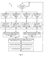
- Fig. 3 is a flow diagram depicting a sequence detection process in accordance with various embodiments of the present invention.
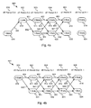
- Figs. 4a-4c depict an example state transition map corresponding to the processes described in the flow diagram of Fig. 3 and/or the circuit depicted in Fig. 2 ;
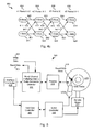
- Fig. 5 shows a storage system including a read channel circuit with interim state sequence detecting in accordance with some embodiments of the present invention.
- the present inventions are related to systems and methods for processing data, and more particularly to systems and methods for detecting data sequences.
- a storage medium 1 is shown with two exemplary tracks 20, 22 indicated as dashed lines.
- the tracks are segregated by servo data written within wedges 19, 18.
- These wedges include servo data 10 that are used for control and synchronization of a read/write head assembly over a desired location on storage medium 1.
- this servo data generally includes a preamble pattern 11 followed by a servo address mark 12 (SAM).
- SAM servo address mark
- Servo address mark 12 is followed by a Gray code 13
- Gray code 13 is followed by burst information 14. It should be noted that while two tracks and two wedges are shown, hundreds of each would typically be included on a given storage medium.
- a servo data set may have two or more fields of burst information. Yet further, it should be noted that different information may be included in the servo fields such as, for example, repeatable run-out information that may appear after burst information 14. Between the servo data bit patterns 10a and 10b, a user data region 16 is provided.
- storage medium 1 is rotated in relation to a sensor that senses information from the storage medium.
- the sensor In a read operation, the sensor would sense servo data from wedge 19 (i.e., during a servo data period) followed by user data from a user data region between wedge 19 and wedge 18 (i.e., during a user data period) and then servo data from wedge 18.
- the sensor In a write operation, the sensor would sense servo data from wedge 19 then write data to the user data region between wedge 19 and wedge 18. Then, the sensor would be switched to sense a remaining portion of the user data region followed by the servo data from wedge 18.
- Various embodiments of the present invention provide systems and methods for sequence detection that rely on a rough equalization to a target response followed by data dependent match filtering correlated to received digital samples. Using this information, a data path traversing a sequence can be determined that maximizes the output of the data dependent match filtering to yield a most likely data sequence.
- a standard Viterbi sequence detector that has a channel memory representing N-1 number of states, where N is the length of the partial response
- one or more embodiments of the present invention utilize two distinct states for detecting binary data.
- Such systems and methods provide for a variety of advantages that may be had in different embodiments of the present invention. For example, in some cases, less precise equalization, timing and gain control than that required by a standard Viterbi detection process may be allowable.
- Data sequence detector circuit 100 includes an analog to digital converter circuit 110 that receives an analog input signal 105, and provides a series of digital samples 115 representing analog input signal 105. Digital samples 115 are synchronized to a 4T sample clock 107.
- Analog to digital converter circuit 110 may be any circuit or system known in the art that is capable of converting a continuous signal into a series of digital samples.
- Analog input signal 107 is a continuous signal representing a number of bit periods. The bit periods recur with a periodicity of T, and the 4T sample clock causes analog to digital converter circuit 110 to generate four samples of analog input signal 105 for each period T.
- Analog input signal 105 may be derived from a variety of sources.
- analog input signal may be received from a read/write head assembly disposed in relation to a storage medium.
- analog input signal may be derived from a receiver circuit that is receiving a wireless transmission. Based upon the disclosure provided herein, one of ordinary skill in the art will recognize a variety of other sources of analog input signal 105.
- Digital samples 115 are provided in parallel to a block of multiplier circuits that each multiply the received digital sample by an array representing a particular transition path. In this case where there are two possible next states from any given prior state, four multiplier circuits are used.
- a multiplier circuit 121 multiplies digital samples 115 by a correlator value 122 representing a transition from a prior zero state to a next zero state.
- a multiplier circuit 123 multiplies digital samples 115 by a correlator value 124 representing a transition from a prior one state to a next zero state.
- a multiplier circuit 125 multiplies digital samples 115 by a correlator value 126 representing a transition from a prior zero state to a next one state.
- a multiplier circuit 127 multiplies digital samples 115 by a correlator value 128 representing a transition from a prior one state to a next one state.
- the resulting products from multiplier circuits 121, 123, 125, 127 are provided to respective adder circuits.
- An adder circuit 131 performs a signed sum the product from multiplier circuit 121 with a prior zero state metric 132 to yield a sum 136
- an adder circuit 135 performs a signed sum the product from multiplier circuit 123 with the same prior zero state metric 132 to yield a sum 139
- An adder circuit 133 performs a signed sum the product from multiplier circuit 123 with a prior one state metric 134 to yield a sum 138
- an adder circuit 137 performs a signed sum the product from multiplier circuit 127 with the same prior one state metric 134 to yield a sum 199.
- Prior zero state metric 132 is the value calculated for the next zero state during processing of the preceding four samples of digital samples 115 and is available from a zero state memory 172.
- prior one state metric 134 is the value calculated for the next one state during processing of the preceding four samples of digital samples 115 and is available from a one state memory 174.
- An interim state metric selector circuit 142 determines which of sum 136 and sum 138 is larger and provides the larger value as an interim output 146. Similarly, an interim state metric selector circuit 144 determines which of sum 139 and sum 199 is larger and provides the larger value as an interim output 148.
- Interim output 146 is provided to zero state memory 172 where it is stored and maintained as prior zero state metric 132 for use in processing the next four samples of digital samples 115.
- Interim output 148 is provided to one state memory 174 where it is stored and maintained as prior one state metric 134 for use in processing the next four samples of digital samples 115.
- Both interim output 146 and interim output 148 are provided to a surviving state metric selector circuit 152 that selects the larger of interim value 146 and interim value 148 as the value of the surviving state.
- the state corresponding to the larger value is the surviving state, and an indication of the surviving state is passed to a state memory and pruning circuit 162.
- State memory and pruning circuit 162 determines a state to state path extending backward from the identified surviving state and resulting in the value selected by surviving state metric selector circuit 152.
- state memory and pruning circuit 162 relies on previously calculated and stored sum values (i.e., sum 136, 138, 139, 199) and prior multiplication products (i.e., products from multipliers 121, 123, 125, 127) for prior periods T.
- analog input signal 105 is provided to analog to digital converter 110.
- Analog input signal 105 represents a number of digital data bits.
- the data represented by analog input signal was wide bi phase encoded prior to writing to a storage medium or transfer via a transmission system.
- a logic zero is represented by the following series of digital samples '1100'
- a logic one is represented by the following series of digital samples '0011'.
- the bit sequence '10011' is encoded as ' 00111100110000110011 ' prior to conversion to the analog signal domain where each bit of the '10011' bit pattern corresponds to a 1T period and each of the encoded bit values corresponds to a period 1T/4.
- a correlator circuit e.g., multiplier 123
- an array [10 -1 -1] i.e., 1->0 correlator value 124
- an array i.e., 0->0 correlator value 122
- [0 1 0 -1] is used by a correlator circuit (i.e., multiplier 121).
- the value of path 931 (i.e., '265') is added to the value of 1 state 920 (i.e., '124') to yield the value of 0 state 910 of '389'.
- the end state of the detected sequence is 1 state 921.
- a zero to one transition path 932 From 0 state 910 two possible paths are shown: a zero to one transition path 932, and a zero to zero transition path 951.
- sufficient historical data has been developed to finish describing the operation of data sequence detector circuit 100 where the historical data is stored to state memory and pruning circuit 162 allowing for tracing a path back through the state options represented by trellis diagram 990 to determine the detected sequence of data bits.
- the next series of four instances of data samples 115 are received as '-76, -42, 70, 52'. These data samples are multiplied by respective correlator values to yield path values for the transitions from zero to zero, from zero to one, from one to zero, and from one to one.
- Interim state metric selector circuit 142 selects the greater of sum 136 and sum 138 and causes the selected value to be written to zero state memory 172.
- Zero state memory 172 outputs the stored value as prior zero state metric 132.
- sum 136 is selected over sum 138, and the larger value (i.e., 310) is provided as interim output 146 to surviving state metric selector circuit 152.
- interim state metric selector circuit 144 selects the greater of sum 139 and sum 199 and causes the selected value to be written to one state memory 174.
- One state memory 174 outputs the stored value as prior one state metric 134.
- sum 139 is selected over sum 199, and the larger value (i.e., 602) is provided as interim output 148 to surviving state metric selector circuit 152.
- surviving state metric selector circuit 152 selects the larger of interim output 146 and interim output 148.
- the surviving state is selected as 1 state 922 as it is associated with the largest interim output, '602'.
- the end state of the detected sequence is 1 state 922.
- sequence output 170 may include more or fewer than the example four bits depending upon the number of bits in an expected sequence.
- a longer sequence may include the storage of more interim path and state values by state memory and pruning circuit 162.
- a shorter sequence may utilize the storage of fewer interim path and state values by state memory and pruning circuit 162. Where only a four bit sequence is detected, memory storing the value of 1 state 920 is removed along with corresponding information is removed (i.e., pruned) from state memory and pruning circuit 162.
- the next series of samples are received as digital samples 115.
- the next four samples are '42, 56, -12, 99'.
- These data samples are multiplied by respective correlator values to yield path values for the transitions from zero to zero, from zero to one, from one to zero, and from one to one.
- Interim state metric selector circuit 142 selects the greater of sum 136 and sum 138 and causes the selected value to be written to zero state memory 172.
- Zero state memory 172 outputs the stored value as prior zero state metric 132.
- sum 138 is selected over sum 136, and the larger value (i.e., 557) is provided as interim output 146 to surviving state metric selector circuit 152.
- interim state metric selector circuit 144 selects the greater of sum 139 and sum 199 and causes the selected value to be written to one state memory 174.
- One state memory 174 outputs the stored value as prior one state metric 134.
- sum 199 is selected over sum 139, and the larger value (i.e., 645) is provided as interim output 148 to surviving state metric selector circuit 152.
- surviving state metric selector circuit 152 selects the larger of interim output 146 and interim output 148.
- the surviving state is selected as 1 state 923 as it is associated with the largest interim output, '645'.
- the end state of the detected sequence is 1 state 923.
- state memory and pruning circuit 162 traces the states that were traversed to result in selected 1 state 923. In this case, the following sequence of states were traversed to yield 1 state 923:
- Fig. 4b the next series of samples are received as digital samples 115.
- the next four samples are '-34, 1, 14, 64'.
- These data samples are multiplied by respective correlator values to yield path values for the transitions from zero to zero, from zero to one, from one to zero, and from one to one.
- Interim state metric selector circuit 142 selects the greater of sum 136 and sum 138 and causes the selected value to be written to zero state memory 172.
- Zero state memory 172 outputs the stored value as prior zero state metric 132.
- sum 138 is selected over sum 136, and the larger value (i.e., 533) is provided as interim output 146 to surviving state metric selector circuit 152.
- interim state metric selector circuit 144 selects the greater of sum 139 and sum 199 and causes the selected value to be written to one state memory 174.
- One state memory 174 outputs the stored value as prior one state metric 134.
- sum 199 is selected over sum 139, and the larger value (i.e., 757) is provided as interim output 148 to surviving state metric selector circuit 152.
- surviving state metric selector circuit 152 selects the larger of interim output 146 and interim output 148.
- the surviving state is selected as 1 state 924 as it is associated with the largest interim output, '757'.
- the end state of the detected sequence is 1 state 924.
- 1 state 924 is provided to state memory and pruning circuit 162.
- state memory and pruning circuit 162 traces the states that were traversed to result in selected 1 state 924.
- Sequence Output 170 0 state 911 , 1 state 922 , 1 state 923.
- 1 state 924 ⁇ 0 1 1 1 ⁇ ⁇ .
- memory storing the value of 0 state 911 1 and the value of paths extending from 0 state 911 are removed (i.e., pruned) from state memory and pruning circuit 162 as shown in a trellis diagram 992 Fig. 4c . This process continues as additional series of data bits are received.
- a flow diagram 200 depicts a sequence detection process in accordance with various embodiments of the present invention.
- 4T samples implies four samples for each bit transition. It should be noted that more or fewer samples per bit transition may be used in relation to different embodiments of the present invention.
- the received samples are multiplied by respective correlator values to yield path values for the transitions from zero to zero, from zero to one, from one to zero, and from one to one.
- the four samples are: 51, -35, -102, -112.
- a prior zero state value is '12' and a prior one state value is '124' .
- a branch metric is calculated of a zero to one transition using a correlator value corresponding to a zero to one transition ('-1 0 11') (block 222).
- a branch metric is calculated of a one to one transition using a correlator value corresponding to a one to one transition ('0-101') (block 224).
- a branch metric is calculated of a one to one transition using a correlator value corresponding to a one to zero transition ('10-1-1') (block 226).
- a branch metric is calculated of a one to one transition using a correlator value corresponding to a zero to zero transition ('010-1') (block 228).
- the branch metrics are added to the value of the state from which the branch metric was derived.
- a state metric is calculated for the zero to one transition state to yield a first interim state (block 232).
- the first interim state value is calculated in accordance with the following equation:
- a first surviving state metric is selected between the previously calculated first interim value and the second interim value (block 242). This is done by selecting the larger of the first interim value and the second interim value which in this example is '47'. This value is stored as the prior one state metric for use in multiplying the next series of data samples (e.g., in blocks 222, 224, 226, 228).
- a second surviving state metric is selected between the previously calculated third interim value and the fourth interim value (block 244). This is done by selecting the larger of the third interim value and the fourth interim value which in this example is '389'. This value is stored as the prior zero state metric for use in multiplying the next series of data samples (e.g., in blocks 222, 224, 226, 228).
- a surviving state metric is selected (block 252). This is done by selecting the larger of the first surviving interim state and the second surviving interim state which in this example is '389'.
- the surviving state metric in this case is the zero state.
- This surviving state metric corresponds to the most recent bit in the detected sequence, and is used to trace back in time to yield the detected bit sequence over the desired number of bits (block 262). This is done by determining prior state metrics in the path that ultimately resulted in the calculation of the value of the surviving state metric.
- the identified bit sequence is then provided as an output (block 272), and the process is repeated for the next series of digital samples that are received (block 210).
- Storage system 300 may be, for example, a hard disk drive.
- the low latency loop recovery includes a data detector circuit that may be any data detector known in the art.
- Storage system 300 also includes a preamplifier 370, an interface controller 320, a hard disk controller 366, a motor controller 368, a spindle motor 372, a disk platter 378, and a read/write head 376.
- Interface controller 320 controls addressing and timing of data to/from disk platter 378.
- the data on disk platter 378 consists of groups of magnetic signals that may be detected by read/write head assembly 376 when the assembly is properly positioned over disk platter 378.
- disk platter 378 includes magnetic signals recorded in accordance with either a longitudinal or a perpendicular recording scheme.
- read/write head assembly 376 is accurately positioned by motor controller 368 over a desired data track on disk platter 378.
- Motor controller 368 both positions read/write head assembly 376 in relation to disk platter 378 and drives spindle motor 372 by moving read/write head assembly to the proper data track on disk platter 378 under the direction of hard disk controller 366.
- Spindle motor 372 spins disk platter 378 at a determined spin rate (RPMs).
- RPMs spin rate
- This minute analog signal is transferred from read/write head assembly 376 to read channel module 364 via preamplifier 370.
- Preamplifier 370 is operable to amplify the minute analog signals accessed from disk platter 378.
- read channel circuit 310 decodes and digitizes the received analog signal to recreate the information originally written to disk platter 378.
- This data is provided as read data 303 to a receiving circuit.
- read channel circuit 310 performs a data sequence detection process to identify various information markers including, but not limited, a preamble in a servo data set to determine the location of read/write head assembly 376 relative to disk platter 378. Such data sequence detection may be performed using the circuit described above in relation to Fig. 2 and/or the method discussed above in relation to Fig. 3a .
- a write operation is substantially the opposite of the preceding read operation with write data 301 being provided to read channel circuit 310. This data is then encoded and written to disk platter 378.
Abstract
Description
- The present inventions are related to systems and methods for processing data, and more particularly to systems and methods for detecting data sequences.
- A typical data processing system receives an analog input signal that is sampled to yield a series of digital samples. The data often includes sequences of data used for data synchronization and/or other purposes. Various existing data processing systems utilize, for example, a Viterbi sequence detection circuit. Such a circuit operates well where the received digital samples of the analog input signal are accurately equalized to a target response and accurate timing and gain control are applied. In some cases, sufficient accuracy is hard to achieve resulting in degraded performance of the sequence detection. Other approaches rely on threshold detection processes that work reasonably well in low noise environments, but as channel bit densities increase the effects of noise increase rendering such threshold approaches less effective.
- Hence, for at least the aforementioned reasons, there exists a need in the art for advanced systems and methods for data sequence detection.
- The present inventions are related to systems and methods for processing data, and more particularly to systems and methods for detecting data sequences.
- According to a first aspect of the present invention, there is provided a method for data detection that includes receiving a series of data samples at a detector circuit; multiplying a portion of the series of data samples by a first correlator value corresponding to a first binary transition to yield a first value; multiplying the portion of the series of data samples by a second correlator value corresponding to a second binary transition to yield a second value; adding the first value to a prior state value to yield a first interim value; adding the second value to the prior state value to yield a second interim value; and selecting the larger of the first interim value and the second interim value to yield a surviving interim value. In some cases, the method may further include storing the surviving interim value as the prior state value.
- In various instances of the aforementioned embodiments, the surviving interim value may be a first surviving interim value and the prior state may be a first prior state. In such instances, the method may further include multiplying the portion of the series of data samples by a third correlator value corresponding to a third binary transition to yield a third value; multiplying the portion of the series of data samples by a fourth correlator value corresponding to a fourth binary transition to yield a fourth value; adding the third value to a second prior state value to yield a third interim value; adding the fourth value to the second prior state value to yield a fourth interim value; and selecting the larger of the third interim value and the fourth interim value to yield a second surviving interim value. In some instances of the aforementioned embodiments, the method may further include storing the second surviving interim value as the second prior state value.
- In various instances of the aforementioned embodiments, the method may further include selecting the larger of the first surviving interim value and the second surviving interim value to yield a surviving state value where the surviving state value is associated with a surviving state. In such cases, the surviving state may be selected as the most recent bit in a bit sequence. In some cases, the method may further include selecting a prior state corresponding to one of the first prior state value and the second prior state value that was used in calculating the selected one of the first surviving interim value and the second surviving interim value as the bit preceding the most recent bit in the bit sequence.
- In one or more instances of the aforementioned embodiments, the first prior state value may correspond to a zero state, and the second prior state value may correspond to a one state. In some cases, the first binary state may be a one state to a zero state transition, the second binary state may be a zero state to a zero state transition, the third binary transition may be a zero state to a one state transition, and the fourth binary transition may be a one state to a one state transition. In one particular case, the first correlator value may be an
array array array 0, -1, 0, 1. - According to another aspect of the present invention there is provided a sequence detector circuit that includes a first, second, third and fourth multiplier circuits, a first, second, third and fourth adder circuits, and a first and second selector circuit. The first multiplier circuit is operable to multiply a series of digital samples by a first correlator value corresponding to a one state to a one state transition to yield a first value. The second multiplier circuit is operable to multiply the series of digital samples by a second correlator value corresponding to a zero state to a one state transition to yield a second value. The third multiplier circuit is operable to multiply the series of digital samples by a third correlator value corresponding to a one state to a zero state transition to yield a third value. The fourth multiplier circuit is operable to multiply the series of digital samples by a fourth correlator value corresponding to a zero state to a zero state transition to yield a fourth value. The first adder circuit is operable to sum the first value and a prior one state value to yield a first interim state value. The second adder circuit is operable to sum the second value and the prior one state value to yield a second interim state value. The third adder circuit is operable to sum the third value and a prior zero state value to yield a third interim state value. The fourth adder circuit is operable to sum the fourth value and the prior zero state value to yield a fourth interim state value. The first selector circuit operable to select the larger of the first interim state value and the second interim state value to yield a first surviving interim state value, and the second selector circuit operable to select the larger of the third interim state value and the fourth interim state value to yield a second surviving interim state value.
- The circuit may further comprise a prior one state memory operable to store the first surviving interim state value as the prior one state value; and a prior zero state memory operable to store the second surviving interim state value as the prior zero state value. The circuit may further comprise a third selector circuit, wherein the third selector circuit is operable to select the larger of the first surviving interim state value and the second surviving interim state value to yield a surviving state value; and a state circuit, wherein the state circuit is operable to identify a state associated with the surviving state value as the most recent bit in a bit sequence.
- The state circuit may be further operable to identify a series of one or more preceding states in a path used to calculate the surviving state value. The state circuit may be further operable to identify a state corresponding to one of the prior zero state value and the prior one state value that was used in calculating the surviving state value as the bit preceding the most recent bit in the bit sequence. The first correlator value may be an
array 0, -1, 0, 1; wherein the second correlator value may be an array -1, 0, 1, 1; wherein the third correlator value may be anarray array - The storage device may further comprise a prior one state memory operable to store the first surviving interim state value as the prior one state value; and a prior zero state memory operable to store the second surviving interim state value as the prior zero state value. The storage device may further comprise a third selector circuit, wherein the third selector circuit is operable to select the larger of the first surviving interim state value and the second surviving interim state value to yield a surviving state value; and a state circuit, wherein the state circuit is operable to identify a state associated with the surviving state value as the most recent bit in a bit sequence. The state circuit may be further operable to identify a state corresponding to one of the prior zero state value and the prior one state value that was used in calculating the surviving state value as the bit preceding the most recent bit in the bit sequence.
- This summary provides only a general outline of some embodiments of the invention. Many other objects, features, advantages and other embodiments of the invention will become more fully apparent from the following detailed description, the appended claims and the accompanying drawings.
- A further understanding of the various embodiments of the present invention may be realized by reference to the figures which are described in remaining portions of the specification. In the figures, like reference numerals are used throughout several figures to refer to similar components. In some instances, a sub-label consisting of a lower case letter is associated with a reference numeral to denote one of multiple similar components. When reference is made to a reference numeral without specification to an existing sub-label, it is intended to refer to all such multiple similar components.
-
Fig. 1 is a block diagram of a known magnetic storage medium and sector data scheme; -
Fig. 2 depicts a data sequence detector circuit in accordance with one or more embodiments of the present invention; -
Fig. 3 is a flow diagram depicting a sequence detection process in accordance with various embodiments of the present invention; -
Figs. 4a-4c depict an example state transition map corresponding to the processes described in the flow diagram ofFig. 3 and/or the circuit depicted inFig. 2 ; and -
Fig. 5 shows a storage system including a read channel circuit with interim state sequence detecting in accordance with some embodiments of the present invention. - The present inventions are related to systems and methods for processing data, and more particularly to systems and methods for detecting data sequences.
- Turning to
Fig. 1 , astorage medium 1 is shown with twoexemplary tracks wedges servo data 10 that are used for control and synchronization of a read/write head assembly over a desired location onstorage medium 1. In particular, this servo data generally includes apreamble pattern 11 followed by a servo address mark 12 (SAM). Servoaddress mark 12 is followed by aGray code 13, and Graycode 13 is followed byburst information 14. It should be noted that while two tracks and two wedges are shown, hundreds of each would typically be included on a given storage medium. Further, it should be noted that a servo data set may have two or more fields of burst information. Yet further, it should be noted that different information may be included in the servo fields such as, for example, repeatable run-out information that may appear after burstinformation 14. Between the servodata bit patterns - In operation,
storage medium 1 is rotated in relation to a sensor that senses information from the storage medium. In a read operation, the sensor would sense servo data from wedge 19 (i.e., during a servo data period) followed by user data from a user data region betweenwedge 19 and wedge 18 (i.e., during a user data period) and then servo data fromwedge 18. In a write operation, the sensor would sense servo data fromwedge 19 then write data to the user data region betweenwedge 19 andwedge 18. Then, the sensor would be switched to sense a remaining portion of the user data region followed by the servo data fromwedge 18. - Various embodiments of the present invention provide systems and methods for sequence detection that rely on a rough equalization to a target response followed by data dependent match filtering correlated to received digital samples. Using this information, a data path traversing a sequence can be determined that maximizes the output of the data dependent match filtering to yield a most likely data sequence. Unlike a standard Viterbi sequence detector that has a channel memory representing N-1 number of states, where N is the length of the partial response, one or more embodiments of the present invention utilize two distinct states for detecting binary data. Such systems and methods provide for a variety of advantages that may be had in different embodiments of the present invention. For example, in some cases, less precise equalization, timing and gain control than that required by a standard Viterbi detection process may be allowable. Where this is the case, increased manufacturing efficiency of products relying on data detection circuits may be achieved due to a reduction in the amount of time allotted to equalization testing. As another example, in some cases, enhanced noise immunity may be achieved when compared with threshold based sequence detection systems. Based upon the disclosure provided herein, one of ordinary skill in the art will recognize a variety of other advantages achievable through implementations of different embodiments of the present invention that may be achieved alternatively to or in addition to the advantages described above,
- Turning to
Fig. 2 , a datasequence detector circuit 100 is shown in accordance with one or more embodiments of the present invention. Datasequence detector circuit 100 includes an analog todigital converter circuit 110 that receives ananalog input signal 105, and provides a series ofdigital samples 115 representinganalog input signal 105.Digital samples 115 are synchronized to a4T sample clock 107. Analog todigital converter circuit 110 may be any circuit or system known in the art that is capable of converting a continuous signal into a series of digital samples.Analog input signal 107 is a continuous signal representing a number of bit periods. The bit periods recur with a periodicity of T, and the 4T sample clock causes analog todigital converter circuit 110 to generate four samples ofanalog input signal 105 for each period T. It should be noted that while the present embodiment is described as utilizing four samples per period, that other embodiments of the present invention may use a lower sampling frequency such as, for example, a 2T clock, or may use a higher sampling frequency such as, for example, an 8T clock or 16T clock. Based upon the disclosure provided herein, one of ordinary skill in the art will recognize a variety of sampling frequencies and corresponding bit periods that may be used in relation to different embodiments of the present invention.Analog input signal 105 may be derived from a variety of sources. For example, analog input signal may be received from a read/write head assembly disposed in relation to a storage medium. As another example, analog input signal may be derived from a receiver circuit that is receiving a wireless transmission. Based upon the disclosure provided herein, one of ordinary skill in the art will recognize a variety of other sources ofanalog input signal 105. -
Digital samples 115 are provided in parallel to a block of multiplier circuits that each multiply the received digital sample by an array representing a particular transition path. In this case where there are two possible next states from any given prior state, four multiplier circuits are used. In particular, amultiplier circuit 121 multipliesdigital samples 115 by acorrelator value 122 representing a transition from a prior zero state to a next zero state. Amultiplier circuit 123 multipliesdigital samples 115 by acorrelator value 124 representing a transition from a prior one state to a next zero state. Amultiplier circuit 125 multipliesdigital samples 115 by acorrelator value 126 representing a transition from a prior zero state to a next one state. Amultiplier circuit 127 multipliesdigital samples 115 by acorrelator value 128 representing a transition from a prior one state to a next one state. The resulting products frommultiplier circuits - An
adder circuit 131 performs a signed sum the product frommultiplier circuit 121 with a prior zero state metric 132 to yield asum 136, and anadder circuit 135 performs a signed sum the product frommultiplier circuit 123 with the same prior zero state metric 132 to yield asum 139. Anadder circuit 133 performs a signed sum the product frommultiplier circuit 123 with a prior onestate metric 134 to yield asum 138, and anadder circuit 137 performs a signed sum the product frommultiplier circuit 127 with the same prior onestate metric 134 to yield asum 199. Prior zero state metric 132 is the value calculated for the next zero state during processing of the preceding four samples ofdigital samples 115 and is available from a zerostate memory 172. Similarly, prior onestate metric 134 is the value calculated for the next one state during processing of the preceding four samples ofdigital samples 115 and is available from a onestate memory 174. - An interim state
metric selector circuit 142 determines which ofsum 136 andsum 138 is larger and provides the larger value as aninterim output 146. Similarly, an interim statemetric selector circuit 144 determines which ofsum 139 andsum 199 is larger and provides the larger value as aninterim output 148.Interim output 146 is provided to zerostate memory 172 where it is stored and maintained as prior zero state metric 132 for use in processing the next four samples ofdigital samples 115.Interim output 148 is provided to onestate memory 174 where it is stored and maintained as prior onestate metric 134 for use in processing the next four samples ofdigital samples 115. - Both
interim output 146 andinterim output 148 are provided to a surviving statemetric selector circuit 152 that selects the larger ofinterim value 146 andinterim value 148 as the value of the surviving state. The state corresponding to the larger value is the surviving state, and an indication of the surviving state is passed to a state memory andpruning circuit 162. State memory andpruning circuit 162 determines a state to state path extending backward from the identified surviving state and resulting in the value selected by surviving statemetric selector circuit 152. In doing so, state memory andpruning circuit 162 relies on previously calculated and stored sum values (i.e.,sum multipliers - In operation,
analog input signal 105 is provided to analog todigital converter 110.Analog input signal 105 represents a number of digital data bits. In some cases, the data represented by analog input signal was wide bi phase encoded prior to writing to a storage medium or transfer via a transmission system. In such an encoding, a logic zero is represented by the following series of digital samples '1100', and a logic one is represented by the following series of digital samples '0011'. As an example, the bit sequence '10011' is encoded as '00111100110000110011' prior to conversion to the analog signal domain where each bit of the '10011' bit pattern corresponds to a 1T period and each of the encoded bit values corresponds to a period 1T/4. - Where a target of [5 5 -5 -5] is used, when the analog signal is retrieved from the storage medium or a transfer medium the preceding example would ideally result in the following digital samples 115 '20 10 0 -10 -20 0 20 0 -20 -10 0 10 20 0 -20 0 20'. As can be seen, in a transition from a logic one to a logic zero
digital samples 115 transition from 20 to 10 to 0 to -10. In this case, where a correlator circuit (e.g., multiplier 123) is used that multiplies the samples '10 0 -10 -20' by an array [10 -1 -1] (i.e., 1->0 correlator value 124) yielding an output value of +40 (i.e., [1 * 10]+[0*0]+[-1 *-10]+[-1 *-20] = 40). Similarly, in a transition from a logic zero to a logic zero an array (i.e., 0->0 correlator value 122) [0 1 0 -1] is used by a correlator circuit (i.e., multiplier 121). In a transition from a logic zero to a logic one an array (i.e., 0->1 1 correlator value 126) [-1 0 1 1] is used by a correlator circuit (i.e., multiplier 125). Finally, in a transition from a logic one to a logic one an array (i.e., 1->1 correlator value 128) [0 -1 0 1] is used by a correlator circuit (i.e., multiplier 127). It should be noted that other encoding approaches and/or correlator values may be used in relation to different embodiments of the present invention. - Noise and timing errors result in something other than ideal sample values being provided as
digital samples 115 from analog todigital converter 110. As an example, assume the followingdigital samples 115 are received synchronous to 4T sample clock 107: - [... 124] [51, -35, -102, -112] [-16,28,48,13] [-76, -42, 70, 52] [42, 56, -12, 99]. In the preceding series of samples, blocks of four samples are grouped with the final sample in each group being the sample that would have been used as the single sample where a simple threshold detector circuit had been used in place of data
sequence detector circuit 100. Of note, where such a simple threshold detection approach is employed, digital samples 115 '124, -112, 13, 52, 99' would yield a detected sequence of '1 0 1 1 1'. As is shown below, datasequence detector circuit 100 yields the correct sequence of '1 0 0 1 1' as it is not as susceptible to noise as a simple threshold detector circuit. - Using the aforementioned series of
digital samples 115 and referring to a trellis diagram 990 ofFig. 4a , an example operation of datasequence detector circuit 100 is further described, Assume that for a bit period 901 (4T period X-4), the one state is the surviving state (i.e., 1 state 920) as selected by statemetric selector circuit 152 with a state value of '124'; and for a bit period 902 (4T period X-3), the zero state is the surviving state (i.e., 0 state 910) as selected by statemetric selector circuit 152 with a state value of '389', and sum 138 corresponding to a one to zerotransition path 931 having a value of '265'. The value '265' is derived by a preceding multiplication bymultiplier 123 of 1->0 correlator value 124 (i.e., [1 0 -1 -1]) by digital samples '51, -35, -102, -112' as follows:
The value of path 931 (i.e., '265') is added to the value of 1 state 920 (i.e., '124') to yield the value of 0state 910 of '389'. Of note, for a bit period 903 (4T period X-2), the end state of the detected sequence is 1state 921. - From 0
state 910 two possible paths are shown: a zero to onetransition path 932, and a zero to zerotransition path 951. The value of zero to onetransition path 932 is calculated wheremultiplier 125 multiplies the next series of four samples (i.e., '-16, 28, 48, 13') by 0->1 correlator value 126 (i.e., [-1 0 1 1]) as follows:
Similarly, the value of zero to zerotransition path 951 is calculated wheremultiplier 121 multiplies the next series of four samples (i.e., '-16, 28, 48, 13') by 0->0 correlator value 122 (i.e., [0 1 0 -1]) as follows:
Adder 135 adds the value ofpath 931 derived frommultiplier 125 to the value of the prior zero state (i.e., the value of 0state 910 which in this example is '389') to yieldsum 139 in accordance with the following equation:
Adder 131 adds the value ofpath 951 derived frommultiplier 121 to the value of the prior zero state (i.e., the value of 0state 910 which in this example is '389') to yieldsum 136 in accordance with the following equation:
At this juncture sufficient historical data has been developed to finish describing the operation of datasequence detector circuit 100 where the historical data is stored to state memory andpruning circuit 162 allowing for tracing a path back through the state options represented by trellis diagram 990 to determine the detected sequence of data bits. - The next series of four instances of
data samples 115 are received as '-76, -42, 70, 52'. These data samples are multiplied by respective correlator values to yield path values for the transitions from zero to zero, from zero to one, from one to zero, and from one to one. In particular, the received data samples are provided tomultiplier 121 where they are multiplied by 0->0 correlator value 122 [0 1 0 -1 ] to yield apath value 952 in accordance with the following equation:
The received data samples are also provided tomultiplier 123 where they are multiplied by 1->0 correlator value 124 [1 0 -1 -1] to yield apath value 941 in accordance with the following equation:
The received data samples are also provided tomultiplier 125 where they are multiplied by 0->1 correlator value 126 [-1011] to yield apath value 933 in accordance with the following equation:
In addition, the received data samples are provided tomultiplier 127 where they are multiplied by 1->1 correlator value 128 [0 -1 0 1] to yield apath value 961 in accordance with the following equation:
- The previously calculated path values are added to the state from which the respective begins to yield corresponding sums. In particular,
path value 952 is provided to adder 131 where it is added to prior zero state metric 132 (i.e., the value of 0state 911 which in this example is '404') to yieldsum 136 in accordance with the following equation:
Path value 941 is provided to adder 133 where it is added to prior one state metric 134 (i.e., the value of 1state 921 which in this example is '466') to yieldsum 138 in accordance with the following equation:
Path value 933 is provided to adder 135 where it is added to prior zero state metric 132 (i.e., the value of 0state 911 which in this example is '404') to yieldsum 139 in accordance with the following equation:
Path value 961 is provided to adder 137 where it is added to prior one state metric 134 (i.e., the value of 1state 921 which in this example is '466') to yieldsum 199 in accordance with the following equation:
- Interim state
metric selector circuit 142 selects the greater ofsum 136 andsum 138 and causes the selected value to be written to zerostate memory 172. Zerostate memory 172 outputs the stored value as prior zerostate metric 132. In this case,sum 136 is selected oversum 138, and the larger value (i.e., 310) is provided asinterim output 146 to surviving statemetric selector circuit 152. Similarly, interim statemetric selector circuit 144 selects the greater ofsum 139 andsum 199 and causes the selected value to be written to onestate memory 174. Onestate memory 174 outputs the stored value as prior onestate metric 134. In this case,sum 139 is selected oversum 199, and the larger value (i.e., 602) is provided asinterim output 148 to surviving statemetric selector circuit 152. In turn, surviving statemetric selector circuit 152 selects the larger ofinterim output 146 andinterim output 148. In this case, the surviving state is selected as 1state 922 as it is associated with the largest interim output, '602'. Thus, for a bit period 904 (4T period X-1), the end state of the detected sequence is 1state 922. - The selection of 1
state 922 is provided to state memory andpruning circuit 162. In turn, state memory andpruning circuit 162 traces the states that were traversed to result in selected 1state 922. In this case, the following sequence of states were traversed to yield 1 state 922:
It should be noted thatsequence output 170 may include more or fewer than the example four bits depending upon the number of bits in an expected sequence. A longer sequence may include the storage of more interim path and state values by state memory andpruning circuit 162. In contrast, a shorter sequence may utilize the storage of fewer interim path and state values by state memory andpruning circuit 162. Where only a four bit sequence is detected, memory storing the value of 1state 920 is removed along with corresponding information is removed (i.e., pruned) from state memory andpruning circuit 162. - The next series of samples are received as
digital samples 115. In this example, the next four samples are '42, 56, -12, 99'. These data samples are multiplied by respective correlator values to yield path values for the transitions from zero to zero, from zero to one, from one to zero, and from one to one. In particular, the received data samples are provided tomultiplier 121 where they are multiplied by 0->0 correlator value 122 [0 1 0 -1] to yield apath value 953 in accordance with the following equation:
The received data samples are also provided tomultiplier 123 where they are multiplied by 1->0 correlator value 124 [1 0 -1 -1] to yield apath value 942 in accordance with the following equation:
The received data samples are also provided tomultiplier 125 where they are multiplied by 0->1 correlator value 126 [-1 0 1 1] to yield apath value 934 in accordance with the following equation:
In addition, the received data samples are provided tomultiplier 127 where they are multiplied by 1->1 correlator value 128 [0 -1 0 1] to yield apath value 962 in accordance with the following equation:
- The previously calculated path values are added to the state from which the respective begins to yield corresponding sums. In particular,
path value 953 is provided to adder 131 where it is added to prior zero state metric 132 (i.e., the value of 0state 912 which in this example is '310') to yieldsum 136 in accordance with the following equation:
Path value 942 is provided to adder 133 where it is added to prior one state metric 134 (i.e., the value of 1state 922 which in this example is '602') to yieldsum 138 in accordance with the following equation:
Path value 934 is provided to adder 135 where it is added to prior zero state metric 132 (i.e., the value of 0state 912 which in this example is '310') to yieldsum 139 in accordance with the following equation:
Path value 962 is provided to adder 137 where it is added to prior one state metric 134 (i.e., the value of 1state 922 which in this example is '602') to yieldsum 199 in accordance with the following equation:
- Interim state
metric selector circuit 142 selects the greater ofsum 136 andsum 138 and causes the selected value to be written to zerostate memory 172. Zerostate memory 172 outputs the stored value as prior zerostate metric 132. In this case,sum 138 is selected oversum 136, and the larger value (i.e., 557) is provided asinterim output 146 to surviving statemetric selector circuit 152. Similarly, interim statemetric selector circuit 144 selects the greater ofsum 139 andsum 199 and causes the selected value to be written to onestate memory 174. Onestate memory 174 outputs the stored value as prior onestate metric 134. In this case,sum 199 is selected oversum 139, and the larger value (i.e., 645) is provided asinterim output 148 to surviving statemetric selector circuit 152. In turn, surviving statemetric selector circuit 152 selects the larger ofinterim output 146 andinterim output 148. In this case, the surviving state is selected as 1state 923 as it is associated with the largest interim output, '645'. Thus, for a bit period 905 (4T period X), the end state of the detected sequence is 1state 923. - The selection of 1
state 923 is provided to state memory andpruning circuit 162. In turn, state memory andpruning circuit 162 traces the states that were traversed to result in selected 1state 923. In this case, the following sequence of states were traversed to yield 1 state 923: -
Sequence Output 170 = [ 0state state state state 910 and the value of paths extending from 0state 910 are removed (i.e., pruned) from state memory andpruning circuit 162 as shown in a trellis diagram 991 ofFig. 4b . - Turning to
Fig. 4b , the next series of samples are received asdigital samples 115. In this example, assume the next four samples are '-34, 1, 14, 64'. These data samples are multiplied by respective correlator values to yield path values for the transitions from zero to zero, from zero to one, from one to zero, and from one to one. In particular, the received data samples are provided tomultiplier 121 where they are multiplied by 0->0 correlator value 122 [0 1 0 -1] to yield apath value 954 in accordance with the following equation:
The received data samples are also provided tomultiplier 123 where they are multiplied by 1->0 correlator value 124 [1 0 -1 -1] to yield apath value 943 in accordance with the following equation:
The received data samples are also provided tomultiplier 125 where they are multiplied by 0-> 1 correlator value 126 [-1011] to yield apath value 935 in accordance with the following equation:
In addition, the received data samples are provided tomultiplier 127 where they are multiplied by 1->1 correlator value 128 [0 1 0 1] to yield apath value 963 in accordance with the following equation:
- The previously calculated path values are added to the state from which the respective begins to yield corresponding sums. In particular,
path value 954 is provided to adder 131 where it is added to prior zero state metric 132 (i.e., the value of 0state 913 which in this example is '355') to yieldsum 136 in accordance with the following equation:
Path value 943 is provided to adder 133 where it is added to prior one state metric 134 (i.e., the value of 1state 923 which in this example is '645') to yieldsum 138 in accordance with the following equation:
Path value 935 is provided to adder 135 where it is added to prior zero state metric 132 (i.e., the value of 0state 913 which in this example is '355') to yieldsum 139 in accordance with the following equation:
Path value 963 is provided to adder 137 where it is added to prior one state metric 134 (i.e., the value of 1state 923 which in this example is '645') to yieldsum 199 in accordance with the following equation:
- Interim state
metric selector circuit 142 selects the greater ofsum 136 andsum 138 and causes the selected value to be written to zerostate memory 172. Zerostate memory 172 outputs the stored value as prior zerostate metric 132. In this case,sum 138 is selected oversum 136, and the larger value (i.e., 533) is provided asinterim output 146 to surviving statemetric selector circuit 152. Similarly, interim statemetric selector circuit 144 selects the greater ofsum 139 andsum 199 and causes the selected value to be written to onestate memory 174. Onestate memory 174 outputs the stored value as prior onestate metric 134. In this case,sum 199 is selected oversum 139, and the larger value (i.e., 757) is provided asinterim output 148 to surviving statemetric selector circuit 152. In turn, surviving statemetric selector circuit 152 selects the larger ofinterim output 146 andinterim output 148. In this case, the surviving state is selected as 1state 924 as it is associated with the largest interim output, '757'. Thus, for a bit period 906 (4T period X+1), the end state of the detected sequence is 1state 924. - The selection of 1
state 924 is provided to state memory andpruning circuit 162. In turn, state memory andpruning circuit 162 traces the states that were traversed to result in selected 1state 924. In this case, the following sequence of states were traversed to yield 1 state 924:
Again, where only a four bit sequence is detected, memory storing the value of 0state 911 1 and the value of paths extending from 0state 911 are removed (i.e., pruned) from state memory andpruning circuit 162 as shown in a trellis diagram 992Fig. 4c . This process continues as additional series of data bits are received. - Turing to
Fig. 3 , a flow diagram 200 depicts a sequence detection process in accordance with various embodiments of the present invention. Following flow diagram 200, it is determined whether 4T samples have been received (block 210). As previously described, 4T samples implies four samples for each bit transition. It should be noted that more or fewer samples per bit transition may be used in relation to different embodiments of the present invention. Once the prescribed number of samples has been received (block 210), the received samples are multiplied by respective correlator values to yield path values for the transitions from zero to zero, from zero to one, from one to zero, and from one to one. As an example, the four samples are: 51, -35, -102, -112. A prior zero state value is '12' and a prior one state value is '124' . In particular, a branch metric is calculated of a zero to one transition using a correlator value corresponding to a zero to one transition ('-1 0 11') (block 222). Using the aforementioned example inputs, the branch metric is calculated in accordance with the following equation:
Similarly, a branch metric is calculated of a one to one transition using a correlator value corresponding to a one to one transition ('0-101') (block 224). Using the aforementioned example inputs, the branch metric is calculated in accordance with the following equation:
A branch metric is calculated of a one to one transition using a correlator value corresponding to a one to zero transition ('10-1-1') (block 226). Using the aforementioned example inputs, the branch metric is calculated in accordance with the following equation:
In addition, a branch metric is calculated of a one to one transition using a correlator value corresponding to a zero to zero transition ('010-1') (block 228). Using the aforementioned example inputs, the branch metric is calculated in accordance with the following equation:
- Once the branch metrics are available, the branch metrics are added to the value of the state from which the branch metric was derived. In particular, a state metric is calculated for the zero to one transition state to yield a first interim state (block 232). Using the aforementioned example inputs, the first interim state value is calculated in accordance with the following equation:
- First Interim Value = Prior Zero State Value + 0->1 Branch Metric = 12-265= -253. A state metric is calculated for the one to one transition state to yield a second interim state (block 234). Using the aforementioned example inputs, the second interim state value is calculated in accordance with the following equation:

- A first surviving state metric is selected between the previously calculated first interim value and the second interim value (block 242). This is done by selecting the larger of the first interim value and the second interim value which in this example is '47'. This value is stored as the prior one state metric for use in multiplying the next series of data samples (e.g., in
blocks blocks - Turning to
Fig. 5 , astorage system 300 including aread channel circuit 310 with interim state sequence detecting is shown in accordance with various embodiments of the present invention.Storage system 300 may be, for example, a hard disk drive. The low latency loop recovery includes a data detector circuit that may be any data detector known in the art.Storage system 300 also includes apreamplifier 370, aninterface controller 320, ahard disk controller 366, amotor controller 368, aspindle motor 372, adisk platter 378, and a read/write head 376.Interface controller 320 controls addressing and timing of data to/fromdisk platter 378. The data ondisk platter 378 consists of groups of magnetic signals that may be detected by read/write head assembly 376 when the assembly is properly positioned overdisk platter 378. In one embodiment,disk platter 378 includes magnetic signals recorded in accordance with either a longitudinal or a perpendicular recording scheme. - In a typical read operation, read/
write head assembly 376 is accurately positioned bymotor controller 368 over a desired data track ondisk platter 378.Motor controller 368 both positions read/write head assembly 376 in relation todisk platter 378 and drivesspindle motor 372 by moving read/write head assembly to the proper data track ondisk platter 378 under the direction ofhard disk controller 366.Spindle motor 372 spinsdisk platter 378 at a determined spin rate (RPMs). Once read/write head assembly 378 is positioned adjacent the proper data track, magnetic signals representing data ondisk platter 378 are sensed by read/write head assembly 376 asdisk platter 378 is rotated byspindle motor 372. The sensed magnetic signals are provided as a continuous, minute analog signal representative of the magnetic data ondisk platter 378. This minute analog signal is transferred from read/write head assembly 376 to read channel module 364 viapreamplifier 370.Preamplifier 370 is operable to amplify the minute analog signals accessed fromdisk platter 378. In turn, readchannel circuit 310 decodes and digitizes the received analog signal to recreate the information originally written todisk platter 378. This data is provided as readdata 303 to a receiving circuit. As part of decoding the received information, readchannel circuit 310 performs a data sequence detection process to identify various information markers including, but not limited, a preamble in a servo data set to determine the location of read/write head assembly 376 relative todisk platter 378. Such data sequence detection may be performed using the circuit described above in relation toFig. 2 and/or the method discussed above in relation toFig. 3a . A write operation is substantially the opposite of the preceding read operation withwrite data 301 being provided to readchannel circuit 310. This data is then encoded and written todisk platter 378. - In conclusion, the invention provides novel systems, devices, methods and arrangements for performing data processing. While detailed descriptions of one or more embodiments of the invention have been given above, various alternatives, modifications, and equivalents will be apparent to those skilled in the art without varying from the spirit of the invention. Therefore, the above description should not be taken as limiting the scope of the invention, which is defined by the appended claims.
In addition, a state metric is calculated for the zero to zero transition state to yield a fourth interim state (block 238). Using the aforementioned example inputs, the third interim state value is calculated in accordance with the following equation:
Claims (15)
- A method for data detection, the method comprising:receiving a series of data samples (115) at a detector circuit (100);multiplying a portion of the series of data samples by a first correlator value (128) corresponding to a first binary transition to yield a first value;multiplying the portion of the series of data samples (115) by a second correlator value (126) corresponding to a second binary transition to yield a second value;adding the first value (124) to a prior state value (134) to yield a first interim value (138);adding the second value (128) to the prior state value (134) to yield a second interim value (199); andselecting the larger of the first interim value and the second interim value to yield a surviving interim value.
- The method of claim 1, wherein the method further comprises:storing the surviving interim value as the prior state value.
- The method of claim 1 or claim 2, wherein the surviving interim value is a first surviving interim value, wherein the prior state is a first prior state, and wherein the method further comprises:multiplying the portion of the series of data samples (115) by a third correlator value (122) corresponding to a third binary transition to yield a third value;multiplying the portion of the series of data samples (115) by a fourth correlator value (126) corresponding to a fourth binary transition to yield a fourth value;adding the third value to a second prior state value (132) to yield a third interim value;adding the fourth value to the second prior state value (132) to yield a fourth interim value; andselecting the larger of the third interim value and the fourth interim value to yield a second surviving interim value.
- The method of claim 3, wherein the method further comprises:storing the second surviving interim value as the second prior state value (132).
- The method of claim 3 or claim 4, wherein the method further comprises:selecting the larger of the first surviving interim value and the second surviving interim value to yield a surviving state value, wherein the surviving state value is associated with a surviving state; andselecting the surviving state as the most recent bit in a bit sequence.
- The method of claim 5, wherein the method further comprises:selecting a prior state corresponding to one of the first prior state value and the second prior state value that was used in calculating the selected one of the first surviving interim value and the second surviving interim value as the bit preceding the most recent bit in the bit sequence.
- The method of any one of claims 3 to 6, wherein the first prior state value corresponds to a zero state, and wherein the second prior state value corresponds to a one state.
- The method of any one of claims 3 to 6, wherein the third binary transition is a zero state to a one state transition; and wherein the fourth binary transition is a one state to a one state transition.
- The method of claim 8, wherein the first binary state is a one state to a zero state transition; and wherein the second binary state is a zero state to a zero state transition.
- The method of claim 9, wherein the first correlator value is an array 1, 0, -1, -1; wheren the second correlator value is an array 0, 1, 0, -1; wherein the third correlator value is an array -1, 0, 1, 1; and wherein the fourth correlator value is an array 0, - 1, 0, 1.
- A sequence detector circuit (100), the circuit comprising:a first multiplier circuit (127) operable to multiply a series of digital samples (115) by a first correlator value (128) corresponding to a one state to a one state transition to yield a first value;a second multiplier circuit (125) operable to multiply the series of digital samples (115) by a second correlator value (126) corresponding to a zero state to a one state transition to yield a second value;a third multiplier circuit (123) operable to multiply the series of digital samples by a third correlator value (124) corresponding to a one state to a zero state transition to yield a third value;a fourth multiplier circuit (121) operable to multiply the series of digital samples (115) by a fourth correlator value (122) corresponding to a zero state to a zero state transition to yield a fourth value;a first adder circuit (137) operable to sum the first value and a prior one state value to yield a first interim state value (199);a second adder circuit (135) operable to sum the second value and the prior one state value to yield a second interim state value;a first selector circuit (144) operable to select the larger of the first interim state value and the second interim state value to yield a first surviving interim state value;a third adder circuit (133) operable to sum the third value and a prior zero state value to yield a third interim state value (138);a fourth adder circuit (131) operable to sum the fourth value and the prior zero state value to yield a fourth interim state value (136); anda second selector circuit (142) operable to select the larger of the third interim state value and the fourth interim state value to yield a second surviving interim state value.
- The circuit of claim 11, wherein the circuit further comprises:a prior one state memory (174) operable to store the first surviving interim state value as the prior one state value;a prior zero state memory (172) operable to store the second surviving interim state value as the prior zero state valuea third selector circuit (152), wherein the third selector circuit is operable to select the larger of the first surviving interim state value (148) and the second surviving interim state value (146) to yield a surviving state value; anda state circuit (162), wherein the state circuit is operable to identify a state associated with the surviving state value as the most recent bit in a bit sequence.
- The circuit of claim 12, wherein the state circuit is further operable to identify a series of one or more preceding states in a path used to calculate the surviving state value and/or the state circuit is further operable to identify a state corresponding to one of the prior zero state value and the prior one state value that was used in calculating the surviving state value as the bit preceding the most recent bit in the bit sequence.
- The circuit of any one of claims 11 to 13, wherein the first correlator value is an array 0, -1, 0, 1 (128); wherein the second correlator value is an array -1, 0, 1, 1 (126); wherein the third correlator value is an array 1, 0, -1, -1 (124); and wherein the fourth correlator value is an array 0, 1, 0, -1 (122).
- A storage device, the storage device comprising:a detector circuit as claimed in any one of claims 11 to 14.
Applications Claiming Priority (1)
| Application Number | Priority Date | Filing Date | Title |
|---|---|---|---|
| US12/851,475 US8566381B2 (en) | 2010-08-05 | 2010-08-05 | Systems and methods for sequence detection in data processing |
Publications (3)
| Publication Number | Publication Date |
|---|---|
| EP2416319A2 true EP2416319A2 (en) | 2012-02-08 |
| EP2416319A3 EP2416319A3 (en) | 2014-03-12 |
| EP2416319B1 EP2416319B1 (en) | 2015-11-11 |
Family
ID=44312294
Family Applications (1)
| Application Number | Title | Priority Date | Filing Date |
|---|---|---|---|
| EP11275074.0A Active EP2416319B1 (en) | 2010-08-05 | 2011-05-04 | Systems and methods for sequence detection in data processing |
Country Status (6)
| Country | Link |
|---|---|
| US (1) | US8566381B2 (en) |
| EP (1) | EP2416319B1 (en) |
| JP (1) | JP5859221B2 (en) |
| KR (1) | KR101466429B1 (en) |
| CN (1) | CN102376329B (en) |
| TW (1) | TWI445321B (en) |
Families Citing this family (15)
| Publication number | Priority date | Publication date | Assignee | Title |
|---|---|---|---|---|
| US8261171B2 (en) | 2011-01-27 | 2012-09-04 | Lsi Corporation | Systems and methods for diversity combined data detection |
| US8565047B2 (en) | 2011-04-28 | 2013-10-22 | Lsi Corporation | Systems and methods for data write loopback based timing control |
| US20130094619A1 (en) * | 2011-10-17 | 2013-04-18 | Qualcomm Incorporated | Systems and methods for packet detection |
| US8773811B2 (en) | 2011-12-12 | 2014-07-08 | Lsi Corporation | Systems and methods for zone servo timing gain recovery |
| US8681444B2 (en) | 2012-06-07 | 2014-03-25 | Lsi Corporation | Multi-zone servo processor |
| US8625216B2 (en) | 2012-06-07 | 2014-01-07 | Lsi Corporation | Servo zone detector |
| US8564897B1 (en) | 2012-06-21 | 2013-10-22 | Lsi Corporation | Systems and methods for enhanced sync mark detection |
| US9019641B2 (en) | 2012-12-13 | 2015-04-28 | Lsi Corporation | Systems and methods for adaptive threshold pattern detection |
| US9053217B2 (en) | 2013-02-17 | 2015-06-09 | Lsi Corporation | Ratio-adjustable sync mark detection system |
| US9424876B2 (en) | 2013-03-14 | 2016-08-23 | Avago Technologies General Ip (Singapore) Pte. Ltd. | Systems and methods for sync mark mis-detection protection |
| US9275655B2 (en) | 2013-06-11 | 2016-03-01 | Avago Technologies General Ip (Singapore) Pte. Ltd. | Timing error detector with diversity loop detector decision feedback |
| US10152999B2 (en) | 2013-07-03 | 2018-12-11 | Avago Technologies International Sales Pte. Limited | Systems and methods for correlation based data alignment |
| US9129650B2 (en) | 2013-07-25 | 2015-09-08 | Avago Technologies General Ip (Singapore) Pte. Ltd. | Array-reader based magnetic recording systems with frequency division multiplexing |
| US9129646B2 (en) | 2013-09-07 | 2015-09-08 | Avago Technologies General Ip (Singapore) Pte. Ltd. | Array-reader based magnetic recording systems with mixed synchronization |
| US9323625B2 (en) | 2013-11-12 | 2016-04-26 | Avago Technologies General Ip (Singapore) Pte. Ltd. | Systems and methods for lost synchronization data set reprocessing |
Family Cites Families (127)
| Publication number | Priority date | Publication date | Assignee | Title |
|---|---|---|---|---|
| US3973183A (en) | 1971-08-20 | 1976-08-03 | Agency Of Industrial Science & Technology | Method and apparatus for detecting uneven magnetic field by a change in resistance of semiconductor element |
| US3973182A (en) | 1971-08-20 | 1976-08-03 | Agency Of Industrial Science & Technology | Method and apparatus for detecting uneven magnetic field by hall effect in semiconductor |
| US4024571A (en) | 1975-08-14 | 1977-05-17 | Rca Corporation | Synchronizing system employing burst crossover detection |
| US4644564A (en) * | 1983-08-05 | 1987-02-17 | International Business Machines Corporation | Decoding the output signal of a partial-response class-IV communication or recording device channel |
| US4571734A (en) * | 1983-08-05 | 1986-02-18 | International Business Machines Corporation | Method and apparatus for decoding the output signal of a partial-response class-IV communication or recording-device channel |
| US4777544A (en) | 1986-08-15 | 1988-10-11 | International Business Machine Corporation | Method and apparatus for in-situ measurement of head/recording medium clearance |
| DE3938520A1 (en) | 1989-11-21 | 1991-05-29 | Teves Gmbh Alfred | METHOD AND SYSTEM FOR MEASURING DATA EVALUATION AND EVALUATION |
| US5130866A (en) | 1990-07-17 | 1992-07-14 | International Business Machines Corporation | Method and circuitry for in-situ measurement of transducer/recording medium clearance and transducer magnetic instability |
| US5278703A (en) | 1991-06-21 | 1994-01-11 | Digital Equipment Corp. | Embedded servo banded format for magnetic disks for use with a data processing system |
| US5309357A (en) | 1992-01-28 | 1994-05-03 | Independent Scintillation Imaging Systems (Isis) Inc. | Scintillation data collecting apparatus and method |
| WO1993026106A1 (en) * | 1992-06-18 | 1993-12-23 | Oki Electric Industry Co., Ltd. | Maximum likelihood sequence estimating device and method therefor |
| US5341249A (en) | 1992-08-27 | 1994-08-23 | Quantum Corporation | Disk drive using PRML class IV sampling data detection with digital adaptive equalization |
| US5377058A (en) | 1992-12-31 | 1994-12-27 | International Business Machines Corporation | Fly height servo control of read/write head suspension |
| US5400201A (en) | 1993-10-25 | 1995-03-21 | Syquest Technology, Inc. | Servo burst pattern for removing offset caused by magnetic distortion and method associated therewith |
| JPH07302938A (en) | 1994-04-28 | 1995-11-14 | Sony Corp | Piezoelectric ceramic transformer and manufacture thereof |
| US5798885A (en) | 1994-06-06 | 1998-08-25 | Fujitsu Limited | Head positioning control for disk apparatus using peak detection, polarity detection and sector mark detection |
| US5594341A (en) | 1994-06-27 | 1997-01-14 | Varian Associates, Inc. | Nuclear magnetic resonance receiver, method and system |
| US5862005A (en) | 1994-10-11 | 1999-01-19 | Quantum Corporation | Synchronous detection of wide bi-phase coded servo information for disk drive |
| JPH08242179A (en) * | 1995-03-02 | 1996-09-17 | Toshiba Corp | Viterbi decoder |
| US5796535A (en) | 1995-05-12 | 1998-08-18 | Cirrus Logic, Inc. | Sampled amplitude read channel employing a user data frequency synthesizer and a servo data frequency synthesizer |
| US5696639A (en) | 1995-05-12 | 1997-12-09 | Cirrus Logic, Inc. | Sampled amplitude read channel employing interpolated timing recovery |
| US5668679A (en) | 1995-12-21 | 1997-09-16 | Quantum Corporation | System for self-servowriting a disk drive |
| US5987562A (en) | 1996-03-08 | 1999-11-16 | Texas Instruments Incorporated | Waveform sampler and method for sampling a signal from a read channel |
| US6023383A (en) | 1996-03-19 | 2000-02-08 | Texas Instruments Incorporated | Error estimation circuit and method for providing a read channel error signal |
| US5787125A (en) | 1996-05-06 | 1998-07-28 | Motorola, Inc. | Apparatus for deriving in-phase and quadrature-phase baseband signals from a communication signal |
| FR2748571B1 (en) | 1996-05-09 | 1998-08-07 | Europ Agence Spatiale | RECEIVER DEVICE FOR A NAVIGATION SYSTEM IN PARTICULAR BY SATELLITE |
| US6005903A (en) * | 1996-07-08 | 1999-12-21 | Mendelovicz; Ephraim | Digital correlator |
| US5844920A (en) | 1996-11-07 | 1998-12-01 | Cirrus Logic, Inc. | Thermal asperity compensation using multiple sync marks for retroactive and split segment data synchronization in a magnetic disk storage system |
| US5892632A (en) | 1996-11-18 | 1999-04-06 | Cirrus Logic, Inc. | Sampled amplitude read channel employing a residue number system FIR filter in an adaptive equalizer and in interpolated timing recovery |
| US5835295A (en) | 1996-11-18 | 1998-11-10 | Cirrus Logice, Inc. | Zero phase restart interpolated timing recovery in a sampled amplitude read channel |
| US5901010A (en) | 1997-02-07 | 1999-05-04 | Cirrus Logic, Inc. | Magnetic disc recording system employing two stage actuators for simultaneous accesses through multiple recording heads |
| US5781129A (en) | 1997-03-03 | 1998-07-14 | Motorola, Inc. | Adaptive encoder circuit for multiple data channels and method of encoding |
| US6411452B1 (en) | 1997-03-11 | 2002-06-25 | Western Digital Technologies, Inc. | Disk drive employing read error tolerant sync mark detection |
| US5970104A (en) | 1997-03-19 | 1999-10-19 | Cadence Design Systems, Inc. | Method and apparatus for generating branch metrics and branch indices for convolutional code Viterbi decoders |
| US6081397A (en) | 1997-04-08 | 2000-06-27 | International Business Machines Corporation | Method and apparatus for SID-to-SID period estimation |
| US6009549A (en) | 1997-05-15 | 1999-12-28 | Cirrus Logic, Inc. | Disk storage system employing error detection and correction of channel coded data, interpolated timing recovery, and retroactive/split-segment symbol synchronization |
| US5955783A (en) | 1997-06-18 | 1999-09-21 | Lsi Logic Corporation | High frequency signal processing chip having signal pins distributed to minimize signal interference |
| US5986830A (en) | 1997-07-30 | 1999-11-16 | Cirrus Logic, Inc. | Read/write channel write precompensation system and method using one or more delay clocks |
| US6493162B1 (en) | 1997-12-05 | 2002-12-10 | Seagate Technology Llc | Frame synchronization for viterbi detector |
| US6111712A (en) | 1998-03-06 | 2000-08-29 | Cirrus Logic, Inc. | Method to improve the jitter of high frequency phase locked loops used in read channels |
| US6158107A (en) | 1998-04-02 | 2000-12-12 | International Business Machines Corporation | Inverted merged MR head with plated notched first pole tip and self-aligned second pole tip |
| JP4087564B2 (en) | 1998-06-30 | 2008-05-21 | 旭化成エレクトロニクス株式会社 | PLL circuit |
| US6208478B1 (en) | 1998-07-07 | 2001-03-27 | Texas Instruments Incorporated | Read clock interface for read channel device |
| US6657802B1 (en) | 1999-04-16 | 2003-12-02 | Infineon Technologies Corporation | Phase assisted synchronization detector |
| US6404829B1 (en) | 1999-06-29 | 2002-06-11 | Oak Technology, Inc. | DC insensitive AGC circuit for optical PRML read channel |
| JP4238425B2 (en) * | 1999-08-03 | 2009-03-18 | ソニー株式会社 | Disk drive device and servo information detection method |
| EP2224436A3 (en) | 2000-01-14 | 2010-11-24 | Panasonic Corporation | Optical disc and optical disc address regarding apparatus and method |
| US6530060B1 (en) | 2000-02-08 | 2003-03-04 | Cirrus Logic, Inc. | Sampled amplitude read channel employing a post processor with a boundary error compensator which compensates for boundary error events in a split-field data sector |
| US6519102B1 (en) | 2000-04-27 | 2003-02-11 | International Business Machines Corporation | Method and apparatus for implementing an in-situ digital harmonic computation facility for direct access storage device (DASD) |
| US6775529B1 (en) | 2000-07-31 | 2004-08-10 | Marvell International Ltd. | Active resistive summer for a transformer hybrid |
| US6717764B2 (en) | 2000-06-02 | 2004-04-06 | Seagate Technology Llc | Method and apparatus for head fly height measurement |
| US6816328B2 (en) | 2000-06-20 | 2004-11-09 | Infineon Technologies North America Corp. | Pseudo-synchronous interpolated timing recovery for a sampled amplitude read channel |
| US6400518B1 (en) | 2000-11-01 | 2002-06-04 | International Business Machines Corporation | Magneto-resistive asymmetry correction circuit |
| US6606048B1 (en) | 2000-11-16 | 2003-08-12 | Marvell International, Ltd. | Method and apparatus for equalizing the digital performance of multiple ADC's |
| US6490110B2 (en) | 2000-12-05 | 2002-12-03 | Cirrus Logic, Inc. | Servo data detection with improved phase shift tolerance |
| JP2002175673A (en) | 2000-12-07 | 2002-06-21 | Nec Corp | Pll circuit, data detecting circuit and disk device |
| JP4112809B2 (en) | 2001-01-31 | 2008-07-02 | 株式会社東芝 | Magnetic disk apparatus of perpendicular magnetic recording system and disk manufacturing method |
| US6603622B1 (en) | 2001-02-28 | 2003-08-05 | Western Digital Technologies, Inc. | Disk drive employing a sync mark detector comprising a matched filter and a dual polarity correlator |
| US6963521B2 (en) | 2001-03-30 | 2005-11-08 | Sony Corporation | Disc drive apparatus |
| JP2002329329A (en) | 2001-04-27 | 2002-11-15 | Sony Corp | Optical disk utilizing phase change recording method and optical disk device |
| WO2002095738A1 (en) | 2001-05-22 | 2002-11-28 | Seagate Technology Llc | Method and system for measuring fly height |
| US7010065B2 (en) * | 2001-05-25 | 2006-03-07 | Hitachi Global Storage Technologies Netherlands B.V. | Method and apparatus for word synchronization with large coding distance and fault tolerance for PRML systems |
| US6633447B2 (en) | 2001-05-25 | 2003-10-14 | Infineon Technologies Ag | Method and apparatus for compensation of second order distortion |
| JP4726337B2 (en) | 2001-06-27 | 2011-07-20 | ルネサスエレクトロニクス株式会社 | One-chip microcomputer |
| US6856183B2 (en) | 2001-10-12 | 2005-02-15 | Agere Systems Inc. | Scheme to improve performance of timing recovery systems for read channels in a disk drive |
| US7082005B2 (en) | 2001-10-24 | 2006-07-25 | Agere Systems Inc. | Servo data detection in the presence or absence of radial incoherence using digital interpolators |
| US6813108B2 (en) | 2001-10-24 | 2004-11-02 | Agere Systems Inc. | Servo data detection in presence of radial incoherence using multiple data detectors |
| JP4109003B2 (en) | 2002-01-21 | 2008-06-25 | 富士通株式会社 | Information recording / reproducing apparatus, signal decoding circuit and method |
| US7126776B1 (en) | 2002-04-17 | 2006-10-24 | Western Digital Technologies, Inc. | Disk drive having a sector clock that is synchronized to the angular speed of the spindle motor |
| US7088533B1 (en) | 2002-04-23 | 2006-08-08 | Maxtor Corporation | Method of self-servo writing in a disk drive using a spiral pattern |
| TW563318B (en) | 2002-05-20 | 2003-11-21 | Via Optical Solution Inc | Timing recovery circuit and method |
| JP2004014090A (en) | 2002-06-11 | 2004-01-15 | Fujitsu Ltd | Data reproduction system, reproduction method and circuit for performing controlling of reproduction system |
| JP2004095047A (en) | 2002-08-30 | 2004-03-25 | Toshiba Corp | Disk storage device and servo address mark detection method for the same |
| US7167335B1 (en) | 2002-12-27 | 2007-01-23 | Matsushita Electric Industrial Co., Ltd. | Systems for variable multi-pass servowriting and self-servowriting |
| US7092462B2 (en) | 2003-01-14 | 2006-08-15 | Agere Systems Inc. | Asynchronous servo RRO detection employing interpolation |
| US7199961B1 (en) | 2003-03-25 | 2007-04-03 | Marvell International Ltd. | Detecting fly height of a head over a storage medium |
| US7136250B1 (en) | 2003-03-25 | 2006-11-14 | Marvell International Ltd. | Detecting fly height of a head over a storage medium |
| US7116504B1 (en) | 2003-03-25 | 2006-10-03 | Marvell International Ltd. | DC-offset compensation loops for magnetic recording system |
| US7002761B1 (en) | 2003-03-27 | 2006-02-21 | Marvell International Ltd. | Demodulation compensation for spiral servo tracks in hard disk drives |
| US6912099B2 (en) * | 2003-05-13 | 2005-06-28 | Agere Systems Inc. | Maximum likelihood detection of asynchronous servo data employing interpolation |
| WO2004102564A1 (en) | 2003-05-16 | 2004-11-25 | Thomson Licensing | Dsp-based data recovery |
| US7191382B2 (en) | 2003-06-02 | 2007-03-13 | Fujitsu Limited | Methods and apparatus for correcting data and error detection codes on the fly |
| US7308057B1 (en) | 2003-06-05 | 2007-12-11 | Maxtor Corporation | Baseline wander compensation for perpendicular recording |
| US7038875B2 (en) | 2003-07-31 | 2006-05-02 | Seagate Technology Llc | Dynamic measurement of head media spacing modulation |
| US7016131B2 (en) | 2003-08-29 | 2006-03-21 | Agency For Science, Technology And Research | Method and implementation of in-situ absolute head medium spacing measurement |
| US7203017B1 (en) | 2003-09-23 | 2007-04-10 | Marvell International Ltd. | Timing recovery for data storage channels with buffered sectors |
| US7620101B1 (en) | 2003-09-24 | 2009-11-17 | Cypress Semiconductor Corporation | Equalizer circuit, communication system, and method that is adaptive to varying launch amplitudes for reducing receiver error |
| US7002767B2 (en) | 2003-09-30 | 2006-02-21 | Agere Systems Inc. | Detection of recorded data employing interpolation with gain compensation |
| KR20060107536A (en) | 2003-11-18 | 2006-10-13 | 소니 가부시끼 가이샤 | Reproduction device and method, recording medium, and program |
| SG125102A1 (en) | 2004-01-21 | 2006-09-29 | Seagate Technology Llc | Head polarity detection algorithm and apparatus |
| US7154689B1 (en) | 2004-02-05 | 2006-12-26 | Maxtor Corporation | Apparatus for writing servo bursts on a disk with servo track pitch based on read element width and methods of manufacturing same |
| US7230789B1 (en) | 2004-04-08 | 2007-06-12 | Maxtor Corporation | Method and apparatus for performing a self-servo write operation in a disk drive using spiral servo information |
| US7180693B2 (en) | 2004-04-14 | 2007-02-20 | Agere Systems Inc. | Method and apparatus for maximum likelihood detection of data employing interpolation with compensation of signal asymmetry |
| US8405924B2 (en) | 2004-04-30 | 2013-03-26 | Agere Systems Llc | Method and apparatus for improved address mark detection |
| US7098833B2 (en) * | 2004-06-04 | 2006-08-29 | Texas Instruments Incorporated | Tri-value decoder circuit and method |
| JP4427392B2 (en) | 2004-06-22 | 2010-03-03 | 株式会社東芝 | Magnetic recording medium, method for manufacturing the same, and magnetic recording / reproducing apparatus |
| US7079342B1 (en) | 2004-07-26 | 2006-07-18 | Marvell International Ltd. | Method and apparatus for asymmetry correction in magnetic recording channels |
| US7248426B1 (en) | 2004-07-30 | 2007-07-24 | Western Digital Technologies, Inc. | Servo writing a disk drive from spiral tracks by shifting a demodulation window an integer number of sync mark intervals |
| US7253984B1 (en) | 2004-09-02 | 2007-08-07 | Maxtor Corporation | Disk drive that generates a position error signal and a fly height signal from a servo burst pattern |
| US7193544B1 (en) | 2004-09-08 | 2007-03-20 | Northrop Grumman Corporation | Parallel, adaptive delta sigma ADC |
| US7206146B2 (en) | 2004-10-27 | 2007-04-17 | Hitachi Global Storage Technologies Netherlands B.V. | Biphase magnetic pattern detector using multiple matched filters for hard disk drive |
| US7248425B2 (en) | 2004-12-14 | 2007-07-24 | Samsung Electronics Co., Ltd. | Disk writing/reproducing apparatus and method |
| US7167328B2 (en) | 2004-12-17 | 2007-01-23 | Agere Systems Inc. | Synchronizing an asynchronously detected servo signal to synchronous servo demodulation |
| US7193798B2 (en) | 2005-01-12 | 2007-03-20 | Agere Systems, Inc. | Method and apparatus for encoding and decoding a runout correction bit pattern of servo field |
| US7362536B1 (en) | 2005-07-08 | 2008-04-22 | Maxtor Corporation | Disk drive that compensates for phase incoherence between radially adjacent servo tracks and methods thereof |
| JP2007087537A (en) | 2005-09-22 | 2007-04-05 | Rohm Co Ltd | Signal processor, signal processing method and storage system |
| US7693243B2 (en) | 2005-09-26 | 2010-04-06 | Via Technologies, Inc. | Method and circuit for timing recovery |
| US7432750B1 (en) | 2005-12-07 | 2008-10-07 | Netlogic Microsystems, Inc. | Methods and apparatus for frequency synthesis with feedback interpolation |
| US7400464B1 (en) | 2006-02-24 | 2008-07-15 | Marvell International Ltd. | Synchronous RRO write |
| JP4413199B2 (en) | 2006-03-23 | 2010-02-10 | 東芝ストレージデバイス株式会社 | Eccentricity correction method, signal processing circuit, magnetic storage device, and perpendicular magnetic recording medium |
| JP4379814B2 (en) | 2006-03-28 | 2009-12-09 | 富士通株式会社 | Storage device, control method, control device, and program |
| US7423827B2 (en) | 2006-04-20 | 2008-09-09 | Agere Systems Inc. | Systems and methods for accessing data from a variable polarity head assembly |
| US7679850B2 (en) | 2006-05-11 | 2010-03-16 | Seagate Technology Llc | Position determination using circular shift codes |
| US7265937B1 (en) | 2006-06-09 | 2007-09-04 | Seagate Technology Llc | Positioning of a head array over a data storage medium |
| US7411531B2 (en) | 2006-06-30 | 2008-08-12 | Agere Systems Inc. | Methods and apparatus for asynchronous sampling of a received signal at a downsampled rate |
| US7525460B1 (en) | 2006-07-13 | 2009-04-28 | Marvell International Ltd. | Timing loop based on analog to digital converter output and method of use |
| FR2904168B1 (en) | 2006-07-18 | 2008-12-19 | Thales Sa | SYSTEM FOR ESTIMATING THE QUALITY OF RECEPTION OF A DIGITAL TRANSMISSION. |
| US20080056403A1 (en) | 2006-09-01 | 2008-03-06 | On Demand Microelectronics | Method and apparatus for timing recovery of pam signals |
| US7499238B2 (en) | 2006-09-22 | 2009-03-03 | Agere Systems Inc. | Systems and methods for improving disk drive synchronization |
| US7643235B2 (en) | 2006-09-28 | 2010-01-05 | Seagate Technology Llc | Synchronization for data communication |
| TWI392297B (en) | 2006-10-06 | 2013-04-01 | Realtek Semiconductor Corp | Method and apparatus for baseline wander compensation in ethernet application |
| US7446690B2 (en) | 2006-11-06 | 2008-11-04 | Atmel Corporation | Apparatus and method for implementing an analog-to-digital converter in programmable logic devices |
| US7420498B2 (en) | 2006-11-22 | 2008-09-02 | Infineon Technologies Ag | Signal converter performing a role |
| US7768730B2 (en) | 2007-04-30 | 2010-08-03 | Broadcom Corporation | Base line control electronics architecture |
| US7602567B2 (en) | 2007-06-28 | 2009-10-13 | Lsi Corporation | Feed-forward DC restoration in a perpendicular magnetic read channel |
| US8102960B2 (en) | 2008-03-28 | 2012-01-24 | Intel Corporation | Adaptation of a digital receiver |
| US8599973B2 (en) | 2008-04-30 | 2013-12-03 | HGST Netherlands B.V. | Detection of synchronization mark from output of matched filter upstream of Viterbi detector |
-
2010
- 2010-08-05 US US12/851,475 patent/US8566381B2/en not_active Expired - Fee Related
-
2011
- 2011-03-17 TW TW100109120A patent/TWI445321B/en not_active IP Right Cessation
- 2011-04-14 CN CN201110092822.3A patent/CN102376329B/en not_active Expired - Fee Related
- 2011-05-04 EP EP11275074.0A patent/EP2416319B1/en active Active
- 2011-05-11 JP JP2011106028A patent/JP5859221B2/en not_active Expired - Fee Related
- 2011-05-24 KR KR1020110049100A patent/KR101466429B1/en active IP Right Grant
Non-Patent Citations (1)
| Title |
|---|
| None |
Also Published As
| Publication number | Publication date |
|---|---|
| TWI445321B (en) | 2014-07-11 |
| EP2416319A3 (en) | 2014-03-12 |
| US20120036173A1 (en) | 2012-02-09 |
| KR101466429B1 (en) | 2014-11-28 |
| JP5859221B2 (en) | 2016-02-10 |
| EP2416319B1 (en) | 2015-11-11 |
| KR20120015420A (en) | 2012-02-21 |
| CN102376329B (en) | 2016-09-14 |
| CN102376329A (en) | 2012-03-14 |
| US8566381B2 (en) | 2013-10-22 |
| TW201208261A (en) | 2012-02-16 |
| JP2012038409A (en) | 2012-02-23 |
Similar Documents
| Publication | Publication Date | Title |
|---|---|---|
| EP2416319B1 (en) | Systems and methods for sequence detection in data processing | |
| KR101034771B1 (en) | Maximum likelihood detection of asynchronous servo data employing interpolation | |
| EP0803158B1 (en) | Wide biphase digital servo information, detection, and estimation for disk drive using viterbi detection | |
| US8614858B2 (en) | Systems and methods for sync mark detection metric computation | |
| US8861111B1 (en) | Two dimensional magnetic recording servo system phase alignment | |
| EP2479754A1 (en) | Circuits and methods for data detection using multiple detectors, storage device | |
| JP2008513927A (en) | Self-adjusting PRML receiver | |
| US7900124B2 (en) | Bit detection for multitrack digital data storage | |
| US7724844B2 (en) | Detection of servo data for a servo system | |
| EP2843662B1 (en) | Systems and methods for multi-level encoding and decoding | |
| US6282251B1 (en) | Modified viterbi detector which accounts for correlated noise | |
| US6002730A (en) | Method for detecting data and device therefor of data storing unit | |
| US8773811B2 (en) | Systems and methods for zone servo timing gain recovery | |
| US8665544B2 (en) | Systems and methods for servo data detection | |
| US7010065B2 (en) | Method and apparatus for word synchronization with large coding distance and fault tolerance for PRML systems | |
| KR100759601B1 (en) | Phase-shift calculation method, and system implementing it, for a finite-impulse-responsefir filter | |
| US9768988B1 (en) | Jointly optimizing signal equalization and bit detection in a read channel | |
| US8874410B2 (en) | Systems and methods for pattern detection | |
| JP3645478B2 (en) | Control data string encoding method and apparatus | |
| JPH11238320A (en) | Signal processing method and recording and reproducing device using it |
Legal Events
| Date | Code | Title | Description |
|---|---|---|---|
| AK | Designated contracting states |
Kind code of ref document: A2 Designated state(s): AL AT BE BG CH CY CZ DE DK EE ES FI FR GB GR HR HU IE IS IT LI LT LU LV MC MK MT NL NO PL PT RO RS SE SI SK SM TR |
|
| AX | Request for extension of the european patent |
Extension state: BA ME |
|
| PUAI | Public reference made under article 153(3) epc to a published international application that has entered the european phase |
Free format text: ORIGINAL CODE: 0009012 |
|
| PUAL | Search report despatched |
Free format text: ORIGINAL CODE: 0009013 |
|
| AK | Designated contracting states |
Kind code of ref document: A3 Designated state(s): AL AT BE BG CH CY CZ DE DK EE ES FI FR GB GR HR HU IE IS IT LI LT LU LV MC MK MT NL NO PL PT RO RS SE SI SK SM TR |
|
| AX | Request for extension of the european patent |
Extension state: BA ME |
|
| RIC1 | Information provided on ipc code assigned before grant |
Ipc: H04L 25/03 20060101ALI20140204BHEP Ipc: H04L 25/497 20060101ALI20140204BHEP Ipc: G11B 20/10 20060101AFI20140204BHEP Ipc: H04L 1/00 20060101ALI20140204BHEP Ipc: H03M 13/41 20060101ALI20140204BHEP |
|
| 17P | Request for examination filed |
Effective date: 20140912 |
|
| RBV | Designated contracting states (corrected) |
Designated state(s): AL AT BE BG CH CY CZ DE DK EE ES FI FR GB GR HR HU IE IS IT LI LT LU LV MC MK MT NL NO PL PT RO RS SE SI SK SM TR |
|
| GRAP | Despatch of communication of intention to grant a patent |
Free format text: ORIGINAL CODE: EPIDOSNIGR1 |
|
| INTG | Intention to grant announced |
Effective date: 20150616 |
|
| GRAS | Grant fee paid |
Free format text: ORIGINAL CODE: EPIDOSNIGR3 |
|
| GRAA | (expected) grant |
Free format text: ORIGINAL CODE: 0009210 |
|
| AK | Designated contracting states |
Kind code of ref document: B1 Designated state(s): AL AT BE BG CH CY CZ DE DK EE ES FI FR GB GR HR HU IE IS IT LI LT LU LV MC MK MT NL NO PL PT RO RS SE SI SK SM TR |
|
| REG | Reference to a national code |
Ref country code: GB Ref legal event code: FG4D |
|
| REG | Reference to a national code |
Ref country code: CH Ref legal event code: EP |
|
| REG | Reference to a national code |
Ref country code: IE Ref legal event code: FG4D |
|
| REG | Reference to a national code |
Ref country code: AT Ref legal event code: REF Ref document number: 760809 Country of ref document: AT Kind code of ref document: T Effective date: 20151215 |
|
| REG | Reference to a national code |
Ref country code: DE Ref legal event code: R096 Ref document number: 602011021346 Country of ref document: DE |
|
| REG | Reference to a national code |
Ref country code: LT Ref legal event code: MG4D |
|
| REG | Reference to a national code |
Ref country code: NL Ref legal event code: MP Effective date: 20160211 |
|
| REG | Reference to a national code |
Ref country code: AT Ref legal event code: MK05 Ref document number: 760809 Country of ref document: AT Kind code of ref document: T Effective date: 20151111 |
|
| PG25 | Lapsed in a contracting state [announced via postgrant information from national office to epo] |
Ref country code: NL Free format text: LAPSE BECAUSE OF FAILURE TO SUBMIT A TRANSLATION OF THE DESCRIPTION OR TO PAY THE FEE WITHIN THE PRESCRIBED TIME-LIMIT Effective date: 20151111 Ref country code: IT Free format text: LAPSE BECAUSE OF FAILURE TO SUBMIT A TRANSLATION OF THE DESCRIPTION OR TO PAY THE FEE WITHIN THE PRESCRIBED TIME-LIMIT Effective date: 20151111 Ref country code: ES Free format text: LAPSE BECAUSE OF FAILURE TO SUBMIT A TRANSLATION OF THE DESCRIPTION OR TO PAY THE FEE WITHIN THE PRESCRIBED TIME-LIMIT Effective date: 20151111 Ref country code: IS Free format text: LAPSE BECAUSE OF FAILURE TO SUBMIT A TRANSLATION OF THE DESCRIPTION OR TO PAY THE FEE WITHIN THE PRESCRIBED TIME-LIMIT Effective date: 20160311 Ref country code: HR Free format text: LAPSE BECAUSE OF FAILURE TO SUBMIT A TRANSLATION OF THE DESCRIPTION OR TO PAY THE FEE WITHIN THE PRESCRIBED TIME-LIMIT Effective date: 20151111 Ref country code: LT Free format text: LAPSE BECAUSE OF FAILURE TO SUBMIT A TRANSLATION OF THE DESCRIPTION OR TO PAY THE FEE WITHIN THE PRESCRIBED TIME-LIMIT Effective date: 20151111 Ref country code: NO Free format text: LAPSE BECAUSE OF FAILURE TO SUBMIT A TRANSLATION OF THE DESCRIPTION OR TO PAY THE FEE WITHIN THE PRESCRIBED TIME-LIMIT Effective date: 20160211 |
|
| PG25 | Lapsed in a contracting state [announced via postgrant information from national office to epo] |
Ref country code: SE Free format text: LAPSE BECAUSE OF FAILURE TO SUBMIT A TRANSLATION OF THE DESCRIPTION OR TO PAY THE FEE WITHIN THE PRESCRIBED TIME-LIMIT Effective date: 20151111 Ref country code: FI Free format text: LAPSE BECAUSE OF FAILURE TO SUBMIT A TRANSLATION OF THE DESCRIPTION OR TO PAY THE FEE WITHIN THE PRESCRIBED TIME-LIMIT Effective date: 20151111 Ref country code: PT Free format text: LAPSE BECAUSE OF FAILURE TO SUBMIT A TRANSLATION OF THE DESCRIPTION OR TO PAY THE FEE WITHIN THE PRESCRIBED TIME-LIMIT Effective date: 20160311 Ref country code: AT Free format text: LAPSE BECAUSE OF FAILURE TO SUBMIT A TRANSLATION OF THE DESCRIPTION OR TO PAY THE FEE WITHIN THE PRESCRIBED TIME-LIMIT Effective date: 20151111 Ref country code: PL Free format text: LAPSE BECAUSE OF FAILURE TO SUBMIT A TRANSLATION OF THE DESCRIPTION OR TO PAY THE FEE WITHIN THE PRESCRIBED TIME-LIMIT Effective date: 20151111 Ref country code: LV Free format text: LAPSE BECAUSE OF FAILURE TO SUBMIT A TRANSLATION OF THE DESCRIPTION OR TO PAY THE FEE WITHIN THE PRESCRIBED TIME-LIMIT Effective date: 20151111 Ref country code: GR Free format text: LAPSE BECAUSE OF FAILURE TO SUBMIT A TRANSLATION OF THE DESCRIPTION OR TO PAY THE FEE WITHIN THE PRESCRIBED TIME-LIMIT Effective date: 20160212 Ref country code: RS Free format text: LAPSE BECAUSE OF FAILURE TO SUBMIT A TRANSLATION OF THE DESCRIPTION OR TO PAY THE FEE WITHIN THE PRESCRIBED TIME-LIMIT Effective date: 20151111 |
|
| PG25 | Lapsed in a contracting state [announced via postgrant information from national office to epo] |
Ref country code: CZ Free format text: LAPSE BECAUSE OF FAILURE TO SUBMIT A TRANSLATION OF THE DESCRIPTION OR TO PAY THE FEE WITHIN THE PRESCRIBED TIME-LIMIT Effective date: 20151111 |
|
| REG | Reference to a national code |
Ref country code: DE Ref legal event code: R097 Ref document number: 602011021346 Country of ref document: DE |
|
| PG25 | Lapsed in a contracting state [announced via postgrant information from national office to epo] |
Ref country code: SM Free format text: LAPSE BECAUSE OF FAILURE TO SUBMIT A TRANSLATION OF THE DESCRIPTION OR TO PAY THE FEE WITHIN THE PRESCRIBED TIME-LIMIT Effective date: 20151111 Ref country code: RO Free format text: LAPSE BECAUSE OF FAILURE TO SUBMIT A TRANSLATION OF THE DESCRIPTION OR TO PAY THE FEE WITHIN THE PRESCRIBED TIME-LIMIT Effective date: 20151111 Ref country code: BE Free format text: LAPSE BECAUSE OF NON-PAYMENT OF DUE FEES Effective date: 20160531 Ref country code: EE Free format text: LAPSE BECAUSE OF FAILURE TO SUBMIT A TRANSLATION OF THE DESCRIPTION OR TO PAY THE FEE WITHIN THE PRESCRIBED TIME-LIMIT Effective date: 20151111 Ref country code: DK Free format text: LAPSE BECAUSE OF FAILURE TO SUBMIT A TRANSLATION OF THE DESCRIPTION OR TO PAY THE FEE WITHIN THE PRESCRIBED TIME-LIMIT Effective date: 20151111 Ref country code: SK Free format text: LAPSE BECAUSE OF FAILURE TO SUBMIT A TRANSLATION OF THE DESCRIPTION OR TO PAY THE FEE WITHIN THE PRESCRIBED TIME-LIMIT Effective date: 20151111 |
|
| PLBE | No opposition filed within time limit |
Free format text: ORIGINAL CODE: 0009261 |
|
| STAA | Information on the status of an ep patent application or granted ep patent |
Free format text: STATUS: NO OPPOSITION FILED WITHIN TIME LIMIT |
|
| 26N | No opposition filed |
Effective date: 20160812 |
|
| PG25 | Lapsed in a contracting state [announced via postgrant information from national office to epo] |
Ref country code: SI Free format text: LAPSE BECAUSE OF FAILURE TO SUBMIT A TRANSLATION OF THE DESCRIPTION OR TO PAY THE FEE WITHIN THE PRESCRIBED TIME-LIMIT Effective date: 20151111 |
|
| PG25 | Lapsed in a contracting state [announced via postgrant information from national office to epo] |
Ref country code: LU Free format text: LAPSE BECAUSE OF FAILURE TO SUBMIT A TRANSLATION OF THE DESCRIPTION OR TO PAY THE FEE WITHIN THE PRESCRIBED TIME-LIMIT Effective date: 20160504 Ref country code: BE Free format text: LAPSE BECAUSE OF FAILURE TO SUBMIT A TRANSLATION OF THE DESCRIPTION OR TO PAY THE FEE WITHIN THE PRESCRIBED TIME-LIMIT Effective date: 20151111 |
|
| REG | Reference to a national code |
Ref country code: CH Ref legal event code: PL |
|
| GBPC | Gb: european patent ceased through non-payment of renewal fee |
Effective date: 20160504 |
|
| PG25 | Lapsed in a contracting state [announced via postgrant information from national office to epo] |
Ref country code: LI Free format text: LAPSE BECAUSE OF NON-PAYMENT OF DUE FEES Effective date: 20160531 Ref country code: CH Free format text: LAPSE BECAUSE OF NON-PAYMENT OF DUE FEES Effective date: 20160531 |
|
| REG | Reference to a national code |
Ref country code: IE Ref legal event code: MM4A |
|
| REG | Reference to a national code |
Ref country code: FR Ref legal event code: ST Effective date: 20170131 |
|
| PG25 | Lapsed in a contracting state [announced via postgrant information from national office to epo] |
Ref country code: FR Free format text: LAPSE BECAUSE OF NON-PAYMENT OF DUE FEES Effective date: 20160531 |
|
| PG25 | Lapsed in a contracting state [announced via postgrant information from national office to epo] |
Ref country code: GB Free format text: LAPSE BECAUSE OF NON-PAYMENT OF DUE FEES Effective date: 20160504 Ref country code: IE Free format text: LAPSE BECAUSE OF NON-PAYMENT OF DUE FEES Effective date: 20160504 |
|
| PG25 | Lapsed in a contracting state [announced via postgrant information from national office to epo] |
Ref country code: CY Free format text: LAPSE BECAUSE OF FAILURE TO SUBMIT A TRANSLATION OF THE DESCRIPTION OR TO PAY THE FEE WITHIN THE PRESCRIBED TIME-LIMIT Effective date: 20151111 Ref country code: HU Free format text: LAPSE BECAUSE OF FAILURE TO SUBMIT A TRANSLATION OF THE DESCRIPTION OR TO PAY THE FEE WITHIN THE PRESCRIBED TIME-LIMIT; INVALID AB INITIO Effective date: 20110504 |
|
| PG25 | Lapsed in a contracting state [announced via postgrant information from national office to epo] |
Ref country code: MK Free format text: LAPSE BECAUSE OF FAILURE TO SUBMIT A TRANSLATION OF THE DESCRIPTION OR TO PAY THE FEE WITHIN THE PRESCRIBED TIME-LIMIT Effective date: 20151111 Ref country code: MT Free format text: LAPSE BECAUSE OF NON-PAYMENT OF DUE FEES Effective date: 20160531 Ref country code: TR Free format text: LAPSE BECAUSE OF FAILURE TO SUBMIT A TRANSLATION OF THE DESCRIPTION OR TO PAY THE FEE WITHIN THE PRESCRIBED TIME-LIMIT Effective date: 20151111 Ref country code: MC Free format text: LAPSE BECAUSE OF FAILURE TO SUBMIT A TRANSLATION OF THE DESCRIPTION OR TO PAY THE FEE WITHIN THE PRESCRIBED TIME-LIMIT Effective date: 20151111 |
|
| PG25 | Lapsed in a contracting state [announced via postgrant information from national office to epo] |
Ref country code: BG Free format text: LAPSE BECAUSE OF FAILURE TO SUBMIT A TRANSLATION OF THE DESCRIPTION OR TO PAY THE FEE WITHIN THE PRESCRIBED TIME-LIMIT Effective date: 20151111 |
|
| REG | Reference to a national code |
Ref country code: DE Ref legal event code: R082 Ref document number: 602011021346 Country of ref document: DE Representative=s name: DILG, HAEUSLER, SCHINDELMANN PATENTANWALTSGESE, DE Ref country code: DE Ref legal event code: R081 Ref document number: 602011021346 Country of ref document: DE Owner name: BROADCOM INTERNATIONAL PTE. LTD., SG Free format text: FORMER OWNER: LSI CORPORATION, MILPITAS, CALIF., US Ref country code: DE Ref legal event code: R082 Ref document number: 602011021346 Country of ref document: DE Representative=s name: DILG HAEUSLER SCHINDELMANN PATENTANWALTSGESELL, DE Ref country code: DE Ref legal event code: R081 Ref document number: 602011021346 Country of ref document: DE Owner name: AVAGO TECHNOLOGIES GENERAL IP (SINGAPORE) PTE., SG Free format text: FORMER OWNER: LSI CORPORATION, MILPITAS, CALIF., US Ref country code: DE Ref legal event code: R081 Ref document number: 602011021346 Country of ref document: DE Owner name: AVAGO TECHNOLOGIES INTERNATIONAL SALES PTE. LI, SG Free format text: FORMER OWNER: LSI CORPORATION, MILPITAS, CALIF., US |
|
| PG25 | Lapsed in a contracting state [announced via postgrant information from national office to epo] |
Ref country code: AL Free format text: LAPSE BECAUSE OF FAILURE TO SUBMIT A TRANSLATION OF THE DESCRIPTION OR TO PAY THE FEE WITHIN THE PRESCRIBED TIME-LIMIT Effective date: 20151111 |
|
| REG | Reference to a national code |
Ref country code: DE Ref legal event code: R082 Ref document number: 602011021346 Country of ref document: DE Representative=s name: DILG, HAEUSLER, SCHINDELMANN PATENTANWALTSGESE, DE Ref country code: DE Ref legal event code: R081 Ref document number: 602011021346 Country of ref document: DE Owner name: BROADCOM INTERNATIONAL PTE. LTD., SG Free format text: FORMER OWNER: AVAGO TECHNOLOGIES GENERAL IP (SINGAPORE) PTE. LTD., SINGAPORE, SG Ref country code: DE Ref legal event code: R082 Ref document number: 602011021346 Country of ref document: DE Representative=s name: DILG HAEUSLER SCHINDELMANN PATENTANWALTSGESELL, DE Ref country code: DE Ref legal event code: R081 Ref document number: 602011021346 Country of ref document: DE Owner name: AVAGO TECHNOLOGIES INTERNATIONAL SALES PTE. LI, SG Free format text: FORMER OWNER: AVAGO TECHNOLOGIES GENERAL IP (SINGAPORE) PTE. LTD., SINGAPORE, SG |
|
| REG | Reference to a national code |
Ref country code: DE Ref legal event code: R081 Ref document number: 602011021346 Country of ref document: DE Owner name: AVAGO TECHNOLOGIES INTERNATIONAL SALES PTE. LI, SG Free format text: FORMER OWNER: AVAGO TECHNOLOGIES INTERNATIONAL SALES PTE. LIMITED, SINGAPORE, SG Ref country code: DE Ref legal event code: R082 Ref document number: 602011021346 Country of ref document: DE Representative=s name: DILG, HAEUSLER, SCHINDELMANN PATENTANWALTSGESE, DE Ref country code: DE Ref legal event code: R081 Ref document number: 602011021346 Country of ref document: DE Owner name: BROADCOM INTERNATIONAL PTE. LTD., SG Free format text: FORMER OWNER: AVAGO TECHNOLOGIES INTERNATIONAL SALES PTE. LIMITED, SINGAPORE, SG |
|
| REG | Reference to a national code |
Ref country code: DE Ref legal event code: R081 Ref document number: 602011021346 Country of ref document: DE Owner name: AVAGO TECHNOLOGIES INTERNATIONAL SALES PTE. LI, SG Free format text: FORMER OWNER: BROADCOM INTERNATIONAL PTE. LTD., SINGAPUR, SG |
|
| PGFP | Annual fee paid to national office [announced via postgrant information from national office to epo] |
Ref country code: DE Payment date: 20230510 Year of fee payment: 13 |