EP2466431A1 - Position indicator - Google Patents
Position indicator Download PDFInfo
- Publication number
- EP2466431A1 EP2466431A1 EP11156991A EP11156991A EP2466431A1 EP 2466431 A1 EP2466431 A1 EP 2466431A1 EP 11156991 A EP11156991 A EP 11156991A EP 11156991 A EP11156991 A EP 11156991A EP 2466431 A1 EP2466431 A1 EP 2466431A1
- Authority
- EP
- European Patent Office
- Prior art keywords
- signal
- electrode
- position indicator
- detecting sensor
- circuit
- Prior art date
- Legal status (The legal status is an assumption and is not a legal conclusion. Google has not performed a legal analysis and makes no representation as to the accuracy of the status listed.)
- Granted
Links
- 230000002708 enhancing effect Effects 0.000 claims abstract description 39
- 230000008859 change Effects 0.000 claims abstract description 22
- 238000001514 detection method Methods 0.000 claims abstract description 20
- 230000003321 amplification Effects 0.000 claims description 34
- 238000003199 nucleic acid amplification method Methods 0.000 claims description 34
- 230000001965 increasing effect Effects 0.000 claims description 10
- 230000000630 rising effect Effects 0.000 claims description 3
- 230000008054 signal transmission Effects 0.000 claims description 2
- 238000006243 chemical reaction Methods 0.000 claims 1
- 239000004020 conductor Substances 0.000 description 132
- 230000002093 peripheral effect Effects 0.000 description 57
- 238000010586 diagram Methods 0.000 description 20
- 230000035945 sensitivity Effects 0.000 description 14
- 238000004804 winding Methods 0.000 description 14
- 230000008878 coupling Effects 0.000 description 11
- 238000010168 coupling process Methods 0.000 description 11
- 238000005859 coupling reaction Methods 0.000 description 11
- 239000003990 capacitor Substances 0.000 description 10
- 230000001681 protective effect Effects 0.000 description 8
- 239000012212 insulator Substances 0.000 description 6
- 230000000694 effects Effects 0.000 description 5
- 239000002184 metal Substances 0.000 description 4
- 238000000034 method Methods 0.000 description 4
- 241001422033 Thestylus Species 0.000 description 3
- 230000000149 penetrating effect Effects 0.000 description 3
- 239000000758 substrate Substances 0.000 description 3
- 230000001360 synchronised effect Effects 0.000 description 3
- 230000005540 biological transmission Effects 0.000 description 2
- 238000004891 communication Methods 0.000 description 2
- 230000003247 decreasing effect Effects 0.000 description 2
- 230000001771 impaired effect Effects 0.000 description 2
- 239000011810 insulating material Substances 0.000 description 2
- 238000003672 processing method Methods 0.000 description 2
- 229920003002 synthetic resin Polymers 0.000 description 2
- 239000000057 synthetic resin Substances 0.000 description 2
- 238000006073 displacement reaction Methods 0.000 description 1
- 229920001971 elastomer Polymers 0.000 description 1
- 230000002349 favourable effect Effects 0.000 description 1
- 230000006872 improvement Effects 0.000 description 1
- 230000004048 modification Effects 0.000 description 1
- 238000012986 modification Methods 0.000 description 1
- 229920006395 saturated elastomer Polymers 0.000 description 1
- 239000004065 semiconductor Substances 0.000 description 1
Images


Classifications
-
- G—PHYSICS
- G06—COMPUTING; CALCULATING OR COUNTING
- G06F—ELECTRIC DIGITAL DATA PROCESSING
- G06F3/00—Input arrangements for transferring data to be processed into a form capable of being handled by the computer; Output arrangements for transferring data from processing unit to output unit, e.g. interface arrangements
- G06F3/01—Input arrangements or combined input and output arrangements for interaction between user and computer
- G06F3/03—Arrangements for converting the position or the displacement of a member into a coded form
- G06F3/041—Digitisers, e.g. for touch screens or touch pads, characterised by the transducing means
- G06F3/046—Digitisers, e.g. for touch screens or touch pads, characterised by the transducing means by electromagnetic means
-
- G—PHYSICS
- G06—COMPUTING; CALCULATING OR COUNTING
- G06F—ELECTRIC DIGITAL DATA PROCESSING
- G06F3/00—Input arrangements for transferring data to be processed into a form capable of being handled by the computer; Output arrangements for transferring data from processing unit to output unit, e.g. interface arrangements
- G06F3/01—Input arrangements or combined input and output arrangements for interaction between user and computer
- G06F3/03—Arrangements for converting the position or the displacement of a member into a coded form
- G06F3/033—Pointing devices displaced or positioned by the user, e.g. mice, trackballs, pens or joysticks; Accessories therefor
- G06F3/0354—Pointing devices displaced or positioned by the user, e.g. mice, trackballs, pens or joysticks; Accessories therefor with detection of 2D relative movements between the device, or an operating part thereof, and a plane or surface, e.g. 2D mice, trackballs, pens or pucks
- G06F3/03545—Pens or stylus
-
- G—PHYSICS
- G06—COMPUTING; CALCULATING OR COUNTING
- G06F—ELECTRIC DIGITAL DATA PROCESSING
- G06F3/00—Input arrangements for transferring data to be processed into a form capable of being handled by the computer; Output arrangements for transferring data from processing unit to output unit, e.g. interface arrangements
- G06F3/01—Input arrangements or combined input and output arrangements for interaction between user and computer
- G06F3/03—Arrangements for converting the position or the displacement of a member into a coded form
- G06F3/041—Digitisers, e.g. for touch screens or touch pads, characterised by the transducing means
- G06F3/0416—Control or interface arrangements specially adapted for digitisers
- G06F3/04162—Control or interface arrangements specially adapted for digitisers for exchanging data with external devices, e.g. smart pens, via the digitiser sensing hardware
-
- G—PHYSICS
- G06—COMPUTING; CALCULATING OR COUNTING
- G06F—ELECTRIC DIGITAL DATA PROCESSING
- G06F3/00—Input arrangements for transferring data to be processed into a form capable of being handled by the computer; Output arrangements for transferring data from processing unit to output unit, e.g. interface arrangements
- G06F3/01—Input arrangements or combined input and output arrangements for interaction between user and computer
- G06F3/03—Arrangements for converting the position or the displacement of a member into a coded form
- G06F3/041—Digitisers, e.g. for touch screens or touch pads, characterised by the transducing means
- G06F3/044—Digitisers, e.g. for touch screens or touch pads, characterised by the transducing means by capacitive means
- G06F3/0441—Digitisers, e.g. for touch screens or touch pads, characterised by the transducing means by capacitive means using active external devices, e.g. active pens, for receiving changes in electrical potential transmitted by the digitiser, e.g. tablet driving signals
-
- G—PHYSICS
- G06—COMPUTING; CALCULATING OR COUNTING
- G06F—ELECTRIC DIGITAL DATA PROCESSING
- G06F3/00—Input arrangements for transferring data to be processed into a form capable of being handled by the computer; Output arrangements for transferring data from processing unit to output unit, e.g. interface arrangements
- G06F3/01—Input arrangements or combined input and output arrangements for interaction between user and computer
- G06F3/03—Arrangements for converting the position or the displacement of a member into a coded form
- G06F3/041—Digitisers, e.g. for touch screens or touch pads, characterised by the transducing means
- G06F3/044—Digitisers, e.g. for touch screens or touch pads, characterised by the transducing means by capacitive means
- G06F3/0442—Digitisers, e.g. for touch screens or touch pads, characterised by the transducing means by capacitive means using active external devices, e.g. active pens, for transmitting changes in electrical potential to be received by the digitiser
-
- G—PHYSICS
- G06—COMPUTING; CALCULATING OR COUNTING
- G06F—ELECTRIC DIGITAL DATA PROCESSING
- G06F3/00—Input arrangements for transferring data to be processed into a form capable of being handled by the computer; Output arrangements for transferring data from processing unit to output unit, e.g. interface arrangements
- G06F3/01—Input arrangements or combined input and output arrangements for interaction between user and computer
- G06F3/03—Arrangements for converting the position or the displacement of a member into a coded form
- G06F3/041—Digitisers, e.g. for touch screens or touch pads, characterised by the transducing means
- G06F3/044—Digitisers, e.g. for touch screens or touch pads, characterised by the transducing means by capacitive means
- G06F3/0446—Digitisers, e.g. for touch screens or touch pads, characterised by the transducing means by capacitive means using a grid-like structure of electrodes in at least two directions, e.g. using row and column electrodes
Definitions
- the present invention relates to a position indicator used in conjunction with a position detecting sensor in which position detection is carried out by detecting a change in capacitance.
- a capacitance type position detecting sensor in which position detection is carried out by detecting a change in capacitance needs a certain level of capacitance or higher (normally about 1 pF) that occurs between the position detecting sensor and a position indicator in order to detect the position of the position indicator with high accuracy.
- an input operation on the position detecting sensor is performed by a fingertip or a dedicated electrostatic pen having a relatively large area at a time of contact. That is, it is difficult from a viewpoint of detection sensitivity to detect a fine input position on the position detecting sensor by an electrostatic pen in the shape of a stylus having a fine tip.
- Patent Document 1 Japanese Patent Laid-Open No. Hei 7-295722
- Patent Document 2 Japanese Patent Laid-Open No. Hei 8-272509
- AC alternating-current
- Patent Document 2 Japanese Patent Laid-Open No. Hei 8-272509
- the AC signal sent out from the position indicator to the position detecting sensor has a large amplitude, thereby enabling position detection even with the position indicator formed by an electrostatic pen having a fine tip.
- Patent Document 1 shows a structure in which a signal oscillator 1 is provided within a signal pen 5, an AC signal of a large amplitude is generated by the signal oscillator 1, and the generated AC signal is applied between a stylus conductor 3 and a ring-shaped conductor 4 in the tip section of the signal pen 5.
- Patent Document 2 shows a structure in which a sine wave generator is provided in a stylus 6, and a sine wave AC signal is boosted by using a transformer and then supplied to a tip 2 of the stylus.
- Patent Document 3 Japanese Patent Laid-Open No. 2007-183809 shows the following structure.
- a tip section 2 of a stylus input device 1 touches the surface of a capacitance type touch panel 51
- a movable contact of a switching circuit 3 is switched to the side of a fixed contact 3a
- a phase comparator 5 is set in an operating state.
- an AC reference signal Vi of a frequency Fo which signal is generated by a reference signal source 54 in a capacitance detection type coordinate input device 50, is received via the tip section 2, and then supplied to one input of the phase comparator 5 via the fixed contact 3a of the switching circuit 3.
- a PLL circuit including the phase comparator 5 is phase-synchronized with the AC reference signal Vi, and outputs a signal of the same frequency as that of the AC reference signal Vi.
- the phase comparator 5 is set in a non-operating state.
- the stylus input device 1 outputs a signal that is phase-synchronized with and having the same frequency as that of the AC reference signal Vi, which is generated in the reference signal source 54 in the capacitance detection type coordinate input device 50 due to a flywheel effect of the PLL circuit.
- a signal having an opposite phase from the output signal and an amplitude Vneg exceeding a power supply voltage Vcc is output via the tip section 2 of the stylus input device 1.
- the position indicators described in Patent Document 1 and Patent Document 2 have an AC signal generator, and have the structure of unidirectional signal transmission for transmitting the AC signal generated in the generator to the position detecting sensor.
- the position indicator need to have the AC signal generator adapted to the AC signal used by the position detecting sensor. Cost is correspondingly increased, and the position indicator compatible with the respective position detecting sensor need to be provided, so that the versatility of the position indicator is impaired.
- the position indicator to which the techniques of Patent Document 3 are applied has a structure of so-called half-duplex communication, in which an AC signal from the position detecting sensor is received by a conductor in the tip of the pen, and an AC signal synchronized with the received signal is generated and sent out from the same conductor in the tip of the pen to the position detecting sensor. That is, in the position indicator of Patent Document 3, the conductor in the tip of the pen is shared for both the reception and transmission of the AC signals, so that reception and transmission cannot be performed simultaneously, and a switch circuit for switching the tip of the pen for a signal receiving period and a signal transmitting period needs to be provided.
- the position indicator of Patent Document 3 has a structure for generating a new signal corresponding to the received AC signal by using the PLL circuit, and thereafter sending out the signal generated by the PLL circuit using the same conductor in the tip of the pen by switching the switch circuit.
- the position indicator of Patent Document 3 includes the switch circuit, the continuity or real-time characteristic of the output AC signal may be impaired.
- the PLL circuit generates a new signal, waveform correlation between the signal waveform of the input signal and the signal waveform of the output signal may not necessarily be guaranteed.
- a position indicator that has a high affinity to a position detecting sensor, has high versatility, and ensures a determined waveform correlation between an input signal and an output signal, by having a structure of so-called full-duplex communication in which a signal input channel and a signal output channel are present independently of each other.
- the position indicator is to be used in conjunction with the position detecting sensor that carries out position detection by detecting a change in capacitance.
- a position indicator for use in conjunction with a position detecting sensor for carrying out position detection by detecting a change in capacitance
- the position indicator includes the following: a first electrode configured to receive an AC signal from the position detecting sensor; a signal enhancing processing circuit configured to subject the AC signal received via the first electrode to predetermined signal enhancing processing; and a second electrode different from the first electrode, the second electrode being supplied with a signal output from the signal enhancing processing circuit.
- the first electrode and the second electrode are both disposed at the same end section of the position indicator.
- An enhanced signal is formed having a determined correlation with the AC signal received via the first electrode from the position detecting sensor, while the enhanced signal is sent out to the position detecting sensor via the second electrode.
- the position detecting sensor detects a change in the received signal of the AC signal at a position indicated by the position indicator according to the present invention, and thereby detects the position indicated by the position indicator.
- the position indicator according to the present invention having the above-described structure subjects the AC signal received from the position detecting sensor via the first electrode to signal enhancing processing by the signal enhancing processing circuit, and then feeds back the AC signal to the position detecting sensor via the second electrode.
- the change in the received signal of the AC signal at the position indicated by the position indicator according to the present invention is increased, so that sensitivity of detection of the position indicator in the position detecting sensor is improved.
- a position indicator that has a simple configuration, has a high affinity to a position detecting sensor, has high versatility, and ensures a determined waveform correlation between an input signal and an output signal, so that position detection can be made with high sensitivity, as a position indicator for use in conjunction with the position detecting sensor that carries out position detection by detecting a change in capacitance.
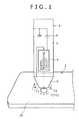
- FIG. 1 is a diagram of assistance in generally explaining a conceptual structure of a position indicator 1 according to a first embodiment of the present invention and a processing operation of the position indicator 1.
- FIG. 1 shows a state in which the position indicator 1 is positioned on a plate surface of a capacitance type position detecting sensor 2.
- FIGS. 2A to 2C are diagrams of assistance in explaining an example of a detailed configuration of the position indicator 1.
- FIG. 2A is a partial longitudinal sectional view of the position indicator 1 and
- FIG. 2B is a partial enlarged view of FIG. 2A.
- FIG. 2C is a diagram showing a part of an external appearance of the position indicator 1.
- the position indicator 1 is formed as a position indicator whose external appearance has the form of a stick-shaped stylus.
- the position indicator 1 has a stick-shaped casing 3-
- This casing 3 is formed by a hollow cylindrical-shaped insulator section 31 made of an insulating material, for example a synthetic resin.
- a conductor section 32 made of a metal, for example.
- a printed wiring board 41 is provided within the casing 3.
- the conductor section 32 covering the outer peripheral surface of the casing 3 is electrically connected to a grounding conductor of the printed wiring board 41.
- a signal processing circuit 4 ( FIG. 1 ) is formed on the printed wiring board 41.
- the signal processing circuit 4 formed on the printed wiring board 41 includes a plurality of electronic parts formed by a resistor, a capacitor, an IC (Integrated Circuit), and the like, wiring patterns such as conducting patterns 42a and 42b and the like, a transformer 43 to be described later, and the like as well as a power supply switch 44, an LED (Light Emitting Diode) 45 and the like in the present example.
- a battery 5 is formed so as to be able to be housed within the casing 3.
- a power supply voltage of the signal processing circuit 4 is generated in the battery 5.
- a terminal 52 in FIG. 2A is a terminal connected electrically to a power supply circuit included in the signal processing circuit 4 on the printed wiring board 41.
- the cathode side electrode 51 of the battery 5 is electrically connected to the terminal 52 in a state of being in contact with the terminal 52.
- an anode side electrode of the battery 5 is directly connected to the grounding conductor of the printed wiring board 41, or brought into pressed-contact with a terminal, which undergoes elastic displacement and is connected to the grounding conductor of the printed wiring board 41 via the conductor section 32 of the casing 3.
- an operating element 44a of the power supply switch 44 disposed on the printed wiring board 41 is provided so as to be externally operable through an opening provided in the casing 3.
- the power supply switch 44 can be turned on or off by sliding movement of the operating element 44a by a user.
- the position indicator 1 is configured such that the LED 45 is lit when power is turned on by turning on the power supply switch 44 by an operation of the operating element 44a, and such that the LED 45 is deactivated when the power is turned off by turning off the power supply switch 44.
- a translucent member 45L is provided at a position corresponding to the position of the LED 45 in the outer peripheral surface of the casing 3. The user can check whether the LED 45 is lit or not through the translucent member 45L.
- a slide operating section 46 is provided in the outer peripheral surface of the casing 3, for allowing a user to manually change the resistance value of a variable resistor 422 provided in the signal processing circuit ( FIG 3 ), to be described later.
- a tapered section 33 that gradually tapers off is formed on one end side in the direction of a center line of the hollow cylindrical-shaped insulator section 31 forming the casing 3.
- a peripheral electrode 6 made of a ring-shaped conducting metal, for example, is attached to the outer circumference side of the tapered section 33.
- the peripheral electrode 6 and the conductor section 32 on the outer peripheral surface of the casing 3 are insulated from each other by the interposition of the insulator section 31 between the peripheral electrode 6 and the conductor section 32.
- the peripheral electrode 6 forms a first electrode in the present example.
- the peripheral electrode 6 is electrically connected to the conducting pattern 42a on the printed wiring board 41 by a lead conducting member 61 penetrating through the insulator section 31.
- the conducting pattern 42a in the present example is connected to an input terminal of the signal processing circuit 4.
- a central electrode 7 is provided so as to project from a hollow part of the tapered section 33 to the outside.
- the central electrode 7 includes for example a stick-shaped conductor 71 made of a conductive metal and an elastic protective conductor 72 provided at an end of the stick-shaped conductor 71.
- the stick-shaped conductor 71 is provided so as to penetrate from the position of the printed wiring board 41 within the casing 3 through the hollow part of the tapered section 33 and project to the outside.
- the elastic protective conductor 72 is a member for preventing the indicating input surface of the position detecting sensor 2 from being scratched and for increasing the area of contact of the position indicator 1 with the indicating input surface when the position indicator 1 is in contact with the position detecting sensor 2.
- the elastic protective conductor 72 is formed by a conductive elastic rubber in the present example. Incidentally, this elastic protective conductor 72 may be omitted. In this case, the stick-shaped conductor 71 is desirably formed by a conductive elastic member, for example.
- the central electrode 7 forms a second electrode in the present example.
- An end part of the stick-shaped conductor 71 on an opposite side from the side where the elastic protective conductor 72 is provided is fixed to the printed wiring board 41, and is electrically connected to the conducting pattern 42b.
- the conducting pattern 42b in the present example is connected to an output terminal of the signal processing circuit 4.
- a shielding member 8 for effectively preventing an electrical interference between the peripheral electrode 6 and the central electrode 7 is provided between the peripheral electrode 6 and the central electrode 7.
- the shielding member 8 is provided so as to surround the central electrode 7. Thereby, the shielding member 8 is interposed between the peripheral electrode 6 and the central electrode 7 to minimize a coupling capacitance between the peripheral electrode 6 and the central electrode 7.
- the shielding member 8 is formed by a tubular conductor 81 made of a conducting metal having an insulating layer 82 formed on an inner wall surface of the tubular conductor 81.
- the tubular conductor 81 is electrically connected to the grounding conductor of the printed wiring board 41.
- the stick-shaped conductor 71 of the central electrode 7 is housed within a hollow part of the tubular conductor 81 having the insulating layer 82 on the inner wall surface of the tubular conductor 81, whereby the central electrode 7 is surrounded by the shielding member 8.
- a part of the elastic protective conductor 72 of the central electrode 7 is also surrounded by the tubular conductor 81 of the shielding member 8.
- the peripheral electrode 6 and the tubular conductor 81 of the shielding member 8 are insulated from each other by the interposition of the tapered section 33 of the insulator section 31 between the peripheral electrode 6 and the tubular conductor 81.
- the central electrode 7 and the tubular conductor 81 of the shielding member 8 are insulated from each other by the interposition of the insulating layer 82 on the inner wall surface of the tubular conductor 81 of the shielding member 8 between the central electrode 7 and the tubular conductor 81.
- peripheral electrode 6 may be shielded instead.
- both of the peripheral electrode 6 and the central electrode 7 may be shielded.
- shielding is provided by surrounding the entire stick-shaped conductor 71 of the central electrode 7 with the shielding member 8, it suffices to interpose the shielding member in at least a part where the peripheral electrode 6 and the central electrode 7 are in proximity to each other.
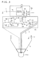
- FIG. 3 is a diagram showing an example of circuit configuration of the signal processing circuit 4.
- the signal processing circuit 4 in the present example includes a power supply circuit section 40a and a signal processing section 40b.
- the power supply circuit section 40a includes a DC-to-DC converter 401.
- the DC-to-DC converter 401 generates a power supply voltage +Vcc from the voltage of the battery 5, and supplies the power supply voltage +Vcc to the signal processing section 40b.
- the power supply circuit section 40a has a power supply switch 44 between the DC-to-DC converter 401 and the battery 5.
- a series circuit of a resistance 402 and the LED 45 is connected between the output terminal of the DC-to-DC converter 401 and the grounding conductor.
- the output terminal of the DC-to-DC converter 401 is connected to the grounding conductor via a series connection of a resistance 403 and a resistance 404.
- the power supply switch 44 when the power supply switch 44 is turned on by operating the operating element 44a provided in the casing 3, the voltage of the battery 5 is supplied to the DC-to-DC converter 401, where the power supply voltage Vcc is generated, and at the same time, the LED 45 is lit to inform the user that the power is on.
- the power supply switch 44 is turned off by operating the operating element 44a, the supply of the voltage of the battery 5 to the DC-to-DC converter 401 is stopped, the generation of the power supply voltage Vcc is stopped, and the LED 45 is turned off to inform the user that the power is off.
- the signal processing section 40b forms a signal enhancing processing circuit.
- the signal processing section 40b in the present embodiment includes a sense amplifier 410, a variable signal amplification factor circuit 420, and a transformer 43.
- Signal enhancing processing performed in the signal enhancing processing circuit in the present invention includes not only processing for amplifying the signal level of an input signal to a determined signal level but also processing for modifying the waveform of the input signal or processing for controlling the phase of the input signal.
- the signal enhancing processing includes increasing a rate of change of the signal level of the input signal in a region where the signal level is low and decreasing the rate of change in a region where the signal waveform is at a maximum value or a minimum value.
- the signal enhancing processing includes forming the signal waveform into a steep signal waveform by increasing a rate of change of the signal level of the input signal in a region of a rising edge of the signal waveform or a region of a falling edge of the signal waveform, or increasing amplitude level in the region. Further, compensation for a phase difference with respect to the input signal, or phase control performed so as to retain a predetermined phase difference, can be applied.
- signal enhancing processing is performed with each of such signal processing methods combined with the above-described signal level amplifying processing, or with each of such signal processing methods applied independently of the signal level amplifying processing.
- the sense amplifier 410 includes an operational amplifier 411 and a capacitor 412 connected between the inverting input terminal and the output terminal of the operational amplifier 411.
- the inverting input terminal of the operational amplifier 411 is connected to a connecting terminal 413 connected to the peripheral electrode 6.
- the non-inverting input terminal of the operational amplifier 411 is supplied with the above-described reference voltage Vref.
- an alternating-current (AC) signal (i.e., a current based on an alternating voltage) flows in the position detecting sensor 2.
- the AC signal is supplied as a current signal to the connecting terminal 413 via the capacitance C 1 and the peripheral electrode 6, and input to the sense amplifier 410.
- the capacitor 412 is to detect the current signal input via the capacitance C1.
- the AC signal may have any waveform. AC signals of any waveform, such as rectangular wave signals, sine wave signals and the like, can be input.
- the sense amplifier 410 inverts the phase of the AC signal input as current signal via the connecting terminal 413, and outputs the resulting AC signal to the variable signal amplification factor circuit 420.
- the variable signal amplification factor circuit 420 includes an operational amplifier 421 and a variable resistor 422 connected between the inverting input terminal and the output terminal of the operational amplifier 421.
- the resistance value of the variable resistor 422 is variably controlled by the user manually by sliding movement of the slide operating section 46 shown in FIG. 2C . Then, by variably setting the resistance value of the variable resistor 422 manually, the amplification factor of the variable signal amplification factor circuit 420 is variably set. As a result, the signal detection sensitivity of the position indicator is controlled.
- the AC signal amplified by the variable signal amplification factor circuit 420 is supplied to the primary winding 43a of the transformer 43.
- the amplitude of an output signal of the variable signal amplification factor circuit 420 is multiplied according to the turns ratio, so that an AC signal (voltage signal) of large amplitude is obtained.
- One end of the secondary winding 43b of the transformer 43 is connected to a connecting terminal 423 connected to the stick-shaped conductor 71 of the central electrode 7 shielded by the shielding member 8. Another end of the secondary winding 43b of the transformer 43 is connected to the grounding conductor of the printed wiring board 41.
- an output signal set as an AC signal voltage of large amplitude by the signal processing section 40b is supplied to the central electrode 7 via the connecting terminal 423.
- the central electrode 7 of the position indicator 1 and the position detecting sensor 2 are coupled to each other via a capacitance. Therefore the AC signal is fed back from the position indicator 1 to the position detecting sensor 2 via the central electrode 7 of the position indicator 1.
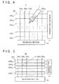
- the capacitance type position detecting sensor 2 in the present example has the configuration of a position detecting sensor of a mutual capacitance system, in which a sensor electrode is composed of an input electrode and an output electrode, and a change in the coupling capacitance of a touch point touched by the position indicator 1 is detected.
- the position detecting sensor 2 in the present example includes a sensor section 20, a transmitting section 21, and a receiving section 22.
- the sensor section 20 includes a plurality of linear transmitting conductors, or 64 transmitting conductors 23Y 1 , 23Y 2, ..., 23Y 64 in the present example, that extend in a lateral direction (X-axis direction) of the indicating input surface as well as a plurality of receiving conductors, or 64 receiving conductors 24X 1 , 24X 2 , ..., 24X 64 in the present example, that are orthogonal to the transmitting conductors 23Y 1 to 23Y 64 and which extend in a longitudinal direction (Y-axis direction) of the indicating input surface.
- the plurality of transmitting conductors 23Y 1 to 23Y 64 are arranged at equal intervals in the Y-axis direction, and are connected to the transmitting section 21.
- the plurality of receiving conductors 24X 1 to 24X 64 are arranged at equal intervals in the X-axis direction, and are connected to the receiving section 22.
- the transmitting conductors 23Y 1 to 23Y 64 when the 64 transmitting conductors 23Y 1 to 23Y 64 do not need to be individually distinguished from each other in the description of the transmitting conductors in the present specification, the transmitting conductors 23Y 1 to 23Y 64 will be referred to as transmitting conductors 23Y Similarly, when the 64 receiving conductors 24X 1 to 24X 64 do not need to be individually distinguished from each other in the description of the receiving conductors, the receiving conductors 24X 1 to 24X 64 will be referred to as receiving conductors 24X.
- the plurality of transmitting conductors 23Y are for example formed in a plane on the lower side of a substrate.
- the plurality of receiving conductors 24X are formed in a plane on the upper side of the substrate.
- the plurality of transmitting conductors 23Y and the plurality of receiving conductors 24X are arranged at a predetermined distance corresponding to a predetermined thickness of the substrate, have an arrangement relation in which the plurality of transmitting conductors 23Y and the plurality of receiving conductors 24X are orthogonal to each other, and form a plurality of points of intersection (cross points).
- a transmitting conductor 23Y and a receiving conductor 24X at each cross point can be considered to be coupled to each other via a predetermined capacitance.
- the transmitting section 21 supplies a predetermined AC signal to the transmitting conductors 23Y.
- the transmitting section 21 may supply an identical AC signal to the plurality of transmitting conductors 23Y 1 , 23Y 2 , ..., 23Y 64 while sequentially selecting the plurality of transmitting conductors 23Y 1 , 23Y 2 , ..., 23Y 64 one at a time, or may simultaneously supply a plurality of AC signals different from each other to the plurality of transmitting conductors 23Y 1 , 23Y 2 , ..., 23Y 64 .
- the plurality of transmitting conductors 23Y 1 , 23Y 2 , ..., 23Y 64 may be divided into a plurality of groups, and different AC signals may be used in different groups.
- the receiving section 22 detects a signal component resulting from the AC signal supplied to the transmitting conductors 23 Y being transmitted to each of the receiving conductors 24X 1 , 24X 2 , ..., 24X 64 via the predetermined capacitance. Supposing that coupling capacitances between the transmitting conductors 23Y and the receiving conductors 24X are equal to each other at all the cross points, the receiving section 22 detects a received signal at a predetermined level from all the receiving conductors 24X 1 , 24X 2 , ..., 24X 64 of the sensor section 20 when the position indicator 1 is not present on the sensor section 20.
- a transmitting conductor 23Y and a receiving conductor 24X forming a cross point at the contact position and the position indicator 1 are coupled to each other via a capacitance. That is, the capacitance at that cross point is changed by the position indicator 1, and the level of a received signal obtained from the receiving conductor 24X at the cross point where the position indicator 1 is present is changed from that of the other cross points.
- the receiving section 22 detects the position of the position indicator 1 by sensing the receiving conductor 24X whose received signal is changed in level among the plurality of receiving conductors 24X 1 , 24X 2 , ..., 24X 64 . Then, a control section of the position detecting sensor 2 (not shown in the figures) detects the cross point touched by the position indicator 1 by detecting the transmitting conductor 23Y, to which the AC signal is supplied from the transmitting section 21, and the receiving conductor 24X whose received signal is changed in level in the receiving section 22.
- the position detecting sensor 2 detects a cross point approached or touched by the finger on similar principles.
- a part of the AC signal supplied to a transmitting conductor 23Y flows through the finger and the human body of the user to the ground. Therefore, a signal received by a receiving conductor 24X forming the cross point where the finger is present is changed in level.
- the receiving section 22 detects the receiving conductor 24X forming the cross point where the finger is present by detecting the change in level of the received signal.
- the position detecting sensor can detect an indicated position on the sensor section 20 on similar principles to those of detection of a finger position.
- an area of contact between the position indicator and the position detecting sensor is not so large as in the case of a finger, thus resulting in a low coupling capacitance and low detection sensitivity of the position detecting sensor.
- the position indicator 1 has a high affinity to the position detecting sensor 2, has high versatility, and ensures a determined waveform correlation between an input signal and an output signal, so that position detection on the sensor section 20 can be made with high sensitivity.
- the peripheral electrode 6 and the sensor section 20 are coupled to each other via the capacitance C1.
- the AC signal supplied to a transmitting conductor 23Y is input as a current signal to the signal processing circuit 4 via the capacitance C1, the peripheral electrode 6, and the connecting terminal 413.
- the AC signal (current signal) input to the signal processing circuit 4 is subjected to signal enhancing processing by being subjected to phase inversion in the sense amplifier 410 of the signal processing section 40b, and thereafter being amplified in the variable signal amplification factor circuit 420 and boosted (multiplied) by the transformer 43, and supplied as a voltage signal to the central electrode 7 via the connecting terminal 423. That is, the AC signal input from the sensor section 20 to the signal processing circuit 4 via the peripheral electrode 6 is converted into a signal of opposite phase and large amplitude in the signal processing section 40b, and fed back to the sensor section 20 via the central electrode 7.
- the AC signal fed back from the central electrode 7 in the position indicator 1 to the sensor section 20 in the position detecting sensor 2 is an enhanced signal of opposite phase from the AC signal supplied to the transmitting conductor 23Y.
- the position indicator 1 therefore functions to further increase a change in the AC signal in the signal received by the receiving conductor 24X.
- the position detecting sensor 2 can thus detect the contact position of the position indicator 1 with high sensitivity.
- detecting operation is further stabilized when the ground of the position indicator 1 is connected to a human body.
- the casing 3 of the position indicator 1 is covered with the conductor section 32 connected to the grounding conductor of the printed wiring board 41 on which the signal processing circuit 4 is formed.
- the AC signal supplied to the transmitting conductor 23Y in the position detecting sensor 2 flows to the ground through the position indicator 1 and the human body of the user, whereby signal detecting operation can be further stabilized.
- V be the voltage of the transmitting conductor 23Y of the sensor section 20 in the position detecting sensor 2
- e be the voltage of the central electrode 7 in the position indicator 1 according to the present embodiment
- C2 be a capacitance between the peripheral electrode 6 and the central electrode 7 (see FIG. 1 )
- e be the voltage of the central electrode 7 in the position indicator 1 according to the present embodiment
- C2 be a capacitance between the peripheral electrode 6 and the central electrode 7 (see FIG. 1 )
- the shielding member 8 is interposed between the peripheral electrode 6 and the central electrode 7, whereby coupling between the peripheral electrode 6 and the central electrode 7 is minimized.
- the interposition of the shielding member 8 can reduce the capacitance C2 between the peripheral electrode 6 and the central electrode 7, increase the voltage e, and enhance sensitivity efficiently.
- the user manually adjusts the slide operating section 46 to vary the resistance value of the variable resistor 422 and to thus variably set the amplification factor of the variable signal amplification factor circuit 420, whereby sensitivity of detection of a position indicated by the position indicator 1 in the position detecting sensor 2 can be adjusted.
- variable signal amplification factor circuit 420 of the signal enhancing processing circuit is configured such that the amplification factor can be changed continuously by the variable resistor 422.
- the variable signal amplification factor circuit 420 may be configured such that the amplification factor can be changed stepwise by selecting a plurality of resistors having different resistance values by a slide switch.
- the position indicator 1 is configured such that the peripheral electrode 6 is set as a first electrode to receive the AC signal from the position detecting sensor 2 and such that the central electrode 7 is set as a second electrode to feed back an enhanced output AC signal to the position detecting sensor 2.
- the central electrode 7 may be set as the first electrode for receiving the AC signal from the position detecting sensor 2
- the peripheral electrode 6 may be set as the second electrode for feeding back an enhanced output AC signal to the position detecting sensor 2.
- the first electrode is the peripheral electrode 6, and the second electrode is the central electrode 7.
- this configuration causes the following problems depending on the configuration of the position detecting sensor 2.
- a sensor section 20A of a position detecting sensor 2A in the example of FIG. 5 includes transmitting conductors 230Y 1 , 230Y 2 , ..., 230Y 64 that do not have a linear shape but have a wide width.
- Other configurations are similar to those of the first embodiment.
- receiving conductors of the sensor section 20A are linear receiving conductors 24X 1 , 24X 2 , ..., 24X 64 as in the first embodiment.
- the plurality of transmitting conductors 230Y 1 , 230Y 2 , ..., 230Y 64 are connected to a transmitting section 21, and the plurality of receiving conductors 24X 1 , 24X 2 , ..., 24X 64 are connected to a receiving section 22.
- the central electrode 7 functions to feed back a larger part of the AC signal to one of the receiving conductors 24X i and 24X i+1 that is closer to the central electrode 7.
- the position detecting sensor 2A detects the locus of movement of the position indicator 1 as a meandering locus.
- the transmitting conductors 230Y 1 , 230Y 2 , ..., 230Y 64 are conductors having a wide width, the AC signal can be received uniformly even when the central electrode 7 is set as the first electrode for receiving the AC signal.
- the peripheral electrode 6 is set as the second electrode for feeding back an enhanced AC signal to the position detecting sensor 2, the peripheral electrode 6 has a larger area of electric engagement with the position detecting sensor 2 than the central electrode 7.
- the peripheral electrode 6 and the two receiving conductors 24X i and 24X i+1 1 adjacent to each other can be respectively set in substantially similar capacitive coupling relations.
- the position detecting sensor 2A can sense the locus of movement of the position indicator as a linear locus.
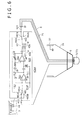
- FIG. 6 is a diagram showing a configuration of a signal processing section 40bA of a signal processing circuit 4A in a position indicator 1A according to the second embodiment.
- the same parts as in the signal processing section 40b of the signal processing circuit 4 according to the first embodiment shown in FIG. 3 are identified by the same reference numerals.
- a connecting terminal 413 connected with the peripheral electrode 6 is connected to one input terminal 481a of a switch 481, and connected to another input terminal 482b of a switch 482.
- a connecting terminal 423 connected with the central electrode 7 is connected to another input terminal 481b of the switch 481, and connected to one input terminal 482a of the switch 482.
- the movable contact 481c of the switch 481 is connected to the inverting input terminal of an operational amplifier 411.
- the movable contact 482c of the switch 482 is connected to one end of the secondary winding 43b of a transformer 43. Otherwise, the signal processing section 40bA is formed in the same manner as the signal processing section 40b described earlier.
- a switching operating element 48 for manually switching switches 481 and 482, which operate in an interlocked manner with each other, is provided so as to be exposed to the outside in a part of the casing 3 of the position indicator 1A according to the second embodiment.
- the switches 481 and 482 are switched to the side of one input terminal 481a and the side of one input terminal 482a in an interlocked manner. Then, the connecting terminals 413 connected with the peripheral electrode 6 is connected to the inverting input terminal of the operational amplifier 411, and the connecting terminal 423 connected with the central electrode 7 is connected to one end of the secondary winding 43b of the transformer 43, so that the position indicator 1A operates in the same manner as in the first embodiment.
- the switches 481 and 482 are switched to the side of the other input terminal 481b and the side of the other input terminal 482b in an interlocked manner. Then, the connecting terminal 423 connected with the central electrode 7 is connected to the inverting input terminal of the operational amplifier 411, and the connecting terminal 413 connected with the peripheral electrode 6 is connected to one end of the secondary winding 43b of the transformer 43.
- the position detecting sensor 2A can detect a position indicated by the position indicator 1A with high sensitivity.
- the transmitting conductors and the receiving conductors of the position detecting sensor are not limited to the above examples. Receiving conductors having a wide width or transmitting conductors and receiving conductors both having a wide width may also be used.
- the user can change the peripheral electrode 6 and the central electrode 7 to the first electrode or the second electrode by the switching operating element 48 according to differences in configuration of these position detecting sensors.
- various position detecting sensors having different configurations of transmitting conductors and receiving conductors can detect the position indicator whose dependence on the position detecting sensors is reduced and which is highly versatile, with higher sensitivity, while avoiding problems corresponding to the different configurations.
- the signal processing sections 40b and 40bA of the signal processing circuits 4 and 4A form a signal enhancing processing circuit with the variable signal amplification factor circuit 420 provided in a stage subsequent to the sense amplifier 410.
- the signal enhancing processing circuit can be of other configurations.
- a third embodiment is a first example of the signal enhancing processing circuit, which enhances an output voltage without using the variable signal amplification factor circuit 420.
- FIG. 7 is a circuit diagram showing an example of configuration of a signal processing section 40bB of a signal processing circuit 4B in the case of a position indicator according to the third embodiment.
- the signal processing section 40bB includes a sense amplifier 410 and an enhancing circuit 430.
- the enhancing circuit 430 includes a transformer 43 and an inverting amplifier circuit 431.
- the output of the sense amplifier 410 is supplied to one end side of the primary winding 43a of the transformer 43 with polarity unchanged, while the output of the sense amplifier 410 is also inverted in polarity by the inverting amplifier circuit 431 and then supplied to the other end side of the primary winding 43a of the transformer 43.
- the secondary winding 43b of the transformer 43 obtains a signal as a result of amplifying the amplitude of the output signal of the sense amplifier 410.
- a reference voltage Vref is supplied to the respective non-inverting input terminals of the operational amplifier 411 and the inverting amplifier circuit 431.
- the enhancing circuit 430 using the transformer 43 can output a signal obtained by enhancing the input signal to the enhancing circuit 430 even with a lower power supply voltage.
- phase and amplitude relation in the case where the signal to be processed is a rectangular wave signal is shown for reference.
- the waveform of the signal as an object of processing in the signal processing section 40bB is not limited to rectangular waves, but may be a signal of any waveform such as that of a sine wave or the like as long as the signal is an AC signal.
- a fourth embodiment is a second example of realizing a signal enhancing processing circuit without using the variable signal amplification factor circuit 420.
- FIG. 8 is a circuit diagram showing an example of configuration of a signal processing section 40bC of a signal processing circuit 4C in the case of a position indicator according to the fourth embodiment.
- the signal processing section 40bC includes a sense amplifier 410 and a waveform converting circuit 440.
- the waveform converting circuit 440 is formed by a comparator circuit 441.
- the sense amplifier 410 has a high amplification factor, which may be an amplification factor such that an output voltage value is saturated, for example.
- the comparator circuit 441 is a waveform converting circuit for comparing an AC signal amplified to a large amplitude by the sense amplifier 410 with a reference voltage Vref, and generating a rectangular wave signal, which has a high level in a section where the amplified signal level is equal to or higher than the reference voltage Vref and which has a low level in other amplified signal level sections.
- the rectangular wave signal from the comparator circuit 441 is further multiplied (boosted) by a transformer 43, and then output as an output signal of the signal processing section 40bC.
- the signal processing section 40bC according to the fourth embodiment can provide an enhanced output signal by converting an input signal into a rectangular wave signal.
- a method for converting the input signal into the rectangular wave signal is not limited to a method represented in FIG. 8 .
- variable signal amplification factor circuit 420 in a stage subsequent to the sense amplifier 410 is configured to allow the user to change the amplification factor manually.
- the variable signal amplification factor circuit 420 can be configured to control the amplification factor automatically.
- the fifth embodiment is an embodiment in that case.
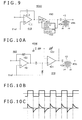
- FIG. 9 is a circuit diagram showing an example of a configuration of a signal processing section 40bD in the fifth embodiment.
- the signal processing section 40bD includes a sense amplifier 410 and an automatic gain adjusting circuit 450.
- the automatic gain adjusting circuit 450 in the present example includes a gain-controlled amplifier 451 of a voltage-controlled type and an output level detecting circuit 452.
- the output signal of the sense amplifier 410 is supplied to the gain-controlled amplifier 451.
- the output level detecting circuit 452 detects the level of the output signal of the gain-controlled amplifier 451, generates a gain adjusting voltage for the gain-controlled amplifier 451, and supplies the gain adjusting voltage to the control terminal of the gain-controlled amplifier 451.
- the gain-controlled amplifier 451 is adjusted in gain by the gain adjusting voltage from the output level detecting circuit 452 so that the level of the output signal of the gain-controlled amplifier 451 is constant at all times. Then, the output signal of the gain-controlled amplifier 451 is boosted by a transformer 43, and output as the output signal of the signal processing section 40bD.
- the position detecting sensor 2 can detect the position indicator 1 with optimum sensitivity at all times irrespective of differences in the users' manner of indicating operations.
- the sense amplifier 410 uses a configuration in which the capacitor 412 is connected between the input and output terminals of the operational amplifier 411, which is common with circuits of this kind.
- the output signal of the sense amplifier 410 has a blunted (dull) waveform compared to the waveform of the input signal of the sense amplifier 410, and a phase delay occurs.
- the receiving section 22 in the position detecting sensor 2 detects a change in a received signal, by detecting an AC signal supplied to a transmitting conductor based on the received signal obtained in a receiving conductor by synchronous detection or correlation operation, it can be difficult to detect the change with high accuracy.
- FIG. 10A is a circuit diagram showing an example of a configuration of a signal processing section 40bE of a signal processing circuit 4E in the sixth embodiment.
- the signal processing section 40bE of the signal processing circuit 4E in the sixth embodiment includes a sense amplifier 460 and a variable signal amplification factor circuit 420 as a signal enhancing processing circuit.
- the sense amplifier 460 includes an operational amplifier 461 and a resistor 462 connected between the inverting input terminal and the output terminal of the operational amplifier 461. That is, this circuit configuration is equal to the configuration in the first embodiment, except that the resistor 462 is connected in place of the capacitor 412 connected between the inverting input terminal and the output terminal of the operational amplifier 461.
- the signal processing section 40bE is otherwise similar to the signal processing section 40b according to the first embodiment.
- a coupling capacitance between the position indicator 1 and the position detecting sensor 2, and the resistor 462 connected between the input and output terminals of the operational amplifier 461 in the sense amplifier 460 together convert an AC signal input from the position detecting sensor 2 to the position indicator 1 into a signal in which high-frequency components are emphasized in the sense amplifier 460.
- the waveform of the output signal of the sense amplifier 460 is a differential waveform whose rising edge and falling edge are emphasized, as shown in FIG. 10C .
- the output signal of the sense amplifier 460 is a phase-compensated signal free from a phase delay with respect to the input signal of the sense amplifier 460, as shown in FIGS. 10B and 10C . That is, the sense amplifier 460 including the operational amplifier 461 provided with the resistor 462 functions also as a phase compensating circuit or a phase control circuit.
- the output signal of the sense amplifier 460 is supplied to the variable signal amplification factor circuit 420 to be further enhanced. Then, the enhanced AC signal is fed back from the position indicator 1 to the position detecting sensor 2.
- the sense amplifier in the sixth embodiment forms a high-frequency emphasizing circuit, while also forming a phase compensating circuit that eliminates a phase delay.
- the receiving section 22 in the position detecting sensor 2 detects a change in a received signal by detecting an AC signal supplied to a transmitting conductor based on the received signal obtained in a receiving conductor by synchronous detection or correlation operation, it is possible to detect the change with high accuracy.
- the AC signal used in the position detecting sensor 2 is a rectangular wave signal with reference to FIGS. 10B and 10C
- the AC signal may be an AC signal of any waveform, such as a sine wave signal or the like.
- FIG 10A is a case where the sixth embodiment is applied to the sense amplifier of the signal processing section 40b according to the first embodiment, the sixth embodiment is also applicable to the sense amplifiers of the signal processing sections according to the second to fifth embodiments.
- a low capacitance between the peripheral electrode 6 and the central electrode 7 is favorable for improvement in sensitivity to the position indicator 1. Therefore, in the first embodiment, the capacitance between the peripheral electrode 6 and the central electrode 7 is minimized by surrounding the central electrode 7 with the shielding member 8.
- the shielding member 8 is formed so as to penetrate through the peripheral electrode 6 and cover the central electrode 7. That is, the shielding member 8 is provided also over a part on the side of the central electrode 7 penetrating beyond the peripheral electrode 6.
- the shielding member 8 may be formed so as to cover the central electrode 7 in a position up to an end part of the peripheral electrode 6 on the side of the central electrode 7 or the vicinity of the end part.
- collar sections 8a and 8b may be formed at the end part of the shielding member 8 penetrating the peripheral electrode 6, as shown in FIGS. 11B and 11C .
- the effect of shielding between the peripheral electrode 6 and the central electrode 7 can be further enhanced by folding the collar section 8a so as to cover the end part of the peripheral electrode 6 as shown in FIG. 11B , or folding the collar section 8b so as to surround the central electrode 7, as shown in FIG. 11C .
- an air space 9 is interposed by providing an air gap between the collar sections 8a and 8b and the peripheral electrode 6 and the tapered section 33 formed of an insulating material.
- a predetermined dielectric may be interposed in place of the air space 9.
- the tapered section 33 formed of a synthetic resin may be extended to the collar sections 8a and 8b.
- a capacitance type detecting sensor of a mutual capacitance system which only detects the coupling capacitance part (XY coordinates) of a touch point between transmitting conductors, to which an AC signal is input, and receiving conductors separated from the transmitting conductors for receiving an AC signal.
- the present invention is similarly applicable to a capacitance type detecting sensor of a self-capacitance system in which the same conductors are used for both inputting and outputting an AC signal.
- a battery is used as a power supply for the position indicator.
- power may for example be supplied from the side of the capacitance type detecting sensor by a wireless system without a battery being provided.
- a configuration may be adopted, in which a resonant circuit producing electromagnetic coupling with a capacitance type detecting sensor and a capacitor, such as an electric double layer capacitor or the like, are provided in a position indicator, and a driving voltage for use is generated from a voltage with which the capacitor is charged.
- a transformer for increasing the signal level is provided on the output side of a signal enhancing processing circuit.
- a signal enhancing circuit formed by a semiconductor circuit may be provided in place of the transformer.
- the conductor section 32 on the periphery of the casing 3 of the position indicator is connected directly (in terms of a direct current) to the grounding conductor of the printed wiring board 41 on which the signal processing circuit 4 is formed within the casing of the position indicator.
- coupling between the grounding conductor of the internal circuit and the conductor section 32 may be provided via a capacitor in terms of an alternating current.
- the conductor section 32 is formed so as to cover substantially the entire periphery of the casing 3 of the position indicator excluding a part insulated from the peripheral electrode.
- a conductive member such as a metallic sheet or the like connected to the grounding conductor of the internal circuit may be disposed on only a predetermined part of the casing 3 to be held by a user so as to be in contact with the human body when the user operates the position indicator.
- the conductor section 32 can be omitted by using a plastic having conductivity and connecting the plastic to the grounding conductor of the internal circuit in terms of a direct current or in terms of an alternating current.
- the position detecting sensor with which the position indicator according to the present invention is used is not limited to tablets, but may be various position detecting sensors used in position detecting devices of various portable terminals, such as pad type terminals and the like and other stationary devices.
Abstract
Description
- The present application claims priority under 35 U.S.C. §119(a) of Japanese Application No.
2010-278002, filed December 14,2010 - The present invention relates to a position indicator used in conjunction with a position detecting sensor in which position detection is carried out by detecting a change in capacitance.
- In general, a capacitance type position detecting sensor in which position detection is carried out by detecting a change in capacitance needs a certain level of capacitance or higher (normally about 1 pF) that occurs between the position detecting sensor and a position indicator in order to detect the position of the position indicator with high accuracy. Thus, an input operation on the position detecting sensor is performed by a fingertip or a dedicated electrostatic pen having a relatively large area at a time of contact. That is, it is difficult from a viewpoint of detection sensitivity to detect a fine input position on the position detecting sensor by an electrostatic pen in the shape of a stylus having a fine tip.
- Various techniques for solving this problem have conventionally been proposed. For example, Patent Document 1 (Japanese Patent Laid-Open No.
Hei 7-295722 Hei 8-272509 Patent Documents - Specifically,
Patent Document 1 shows a structure in which asignal oscillator 1 is provided within asignal pen 5, an AC signal of a large amplitude is generated by thesignal oscillator 1, and the generated AC signal is applied between astylus conductor 3 and a ring-shaped conductor 4 in the tip section of thesignal pen 5.Patent Document 2 shows a structure in which a sine wave generator is provided in astylus 6, and a sine wave AC signal is boosted by using a transformer and then supplied to atip 2 of the stylus. - Patent Document 3 (Japanese Patent Laid-Open No.
2007-183809 tip section 2 of astylus input device 1 touches the surface of a capacitancetype touch panel 51, a movable contact of aswitching circuit 3 is switched to the side of a fixed contact 3a, and aphase comparator 5 is set in an operating state. As a result, an AC reference signal Vi of a frequency Fo, which signal is generated by a reference signal source 54 in a capacitance detection type coordinate input device 50, is received via thetip section 2, and then supplied to one input of thephase comparator 5 via the fixed contact 3a of theswitching circuit 3. Because of this structure, a PLL circuit including thephase comparator 5 is phase-synchronized with the AC reference signal Vi, and outputs a signal of the same frequency as that of the AC reference signal Vi. When the movable contact of theswitching circuit 3 is switched to a fixed contact 3b, thephase comparator 5 is set in a non-operating state. However, thestylus input device 1 outputs a signal that is phase-synchronized with and having the same frequency as that of the AC reference signal Vi, which is generated in the reference signal source 54 in the capacitance detection type coordinate input device 50 due to a flywheel effect of the PLL circuit. A signal having an opposite phase from the output signal and an amplitude Vneg exceeding a power supply voltage Vcc is output via thetip section 2 of thestylus input device 1. -
- [Patent Document 1]
Japanese Patent Laid-Open No.Hei 7-295722 - [Patent Document 2]
Japanese Patent Laid-Open No.Hei 8-272509 - [Patent Document 3]
Japanese Patent Laid-Open No.2007-183809 - However, the position indicators described in
Patent Document 1 andPatent Document 2 have an AC signal generator, and have the structure of unidirectional signal transmission for transmitting the AC signal generated in the generator to the position detecting sensor. Thus, the position indicator need to have the AC signal generator adapted to the AC signal used by the position detecting sensor. Cost is correspondingly increased, and the position indicator compatible with the respective position detecting sensor need to be provided, so that the versatility of the position indicator is impaired. - The position indicator to which the techniques of
Patent Document 3 are applied has a structure of so-called half-duplex communication, in which an AC signal from the position detecting sensor is received by a conductor in the tip of the pen, and an AC signal synchronized with the received signal is generated and sent out from the same conductor in the tip of the pen to the position detecting sensor. That is, in the position indicator ofPatent Document 3, the conductor in the tip of the pen is shared for both the reception and transmission of the AC signals, so that reception and transmission cannot be performed simultaneously, and a switch circuit for switching the tip of the pen for a signal receiving period and a signal transmitting period needs to be provided. - In addition, in the position indicator of
Patent Document 3, an output AC signal in opposite phase from and in synchronism with the received AC signal is generated by the PLL circuit only in the signal receiving period. Then, in the signal transmitting period, the signal from the PLL circuit is output as the output AC signal. Thus, signal continuity or phase relation between the received AC signal and the output AC signal may not necessarily be guaranteed. - As described above, the position indicator of
Patent Document 3 has a structure for generating a new signal corresponding to the received AC signal by using the PLL circuit, and thereafter sending out the signal generated by the PLL circuit using the same conductor in the tip of the pen by switching the switch circuit. Thus, because the position indicator ofPatent Document 3 includes the switch circuit, the continuity or real-time characteristic of the output AC signal may be impaired. In addition, because the PLL circuit generates a new signal, waveform correlation between the signal waveform of the input signal and the signal waveform of the output signal may not necessarily be guaranteed. - In view of the above points, according to one aspect of the present invention, a position indicator is provided that has a high affinity to a position detecting sensor, has high versatility, and ensures a determined waveform correlation between an input signal and an output signal, by having a structure of so-called full-duplex communication in which a signal input channel and a signal output channel are present independently of each other. The position indicator is to be used in conjunction with the position detecting sensor that carries out position detection by detecting a change in capacitance.
- In order to solve the above-described problems, a position indicator according to the present invention is a position indicator for use in conjunction with a position detecting sensor for carrying out position detection by detecting a change in capacitance, and the position indicator includes the following: a first electrode configured to receive an AC signal from the position detecting sensor; a signal enhancing processing circuit configured to subject the AC signal received via the first electrode to predetermined signal enhancing processing; and a second electrode different from the first electrode, the second electrode being supplied with a signal output from the signal enhancing processing circuit. The first electrode and the second electrode are both disposed at the same end section of the position indicator. An enhanced signal is formed having a determined correlation with the AC signal received via the first electrode from the position detecting sensor, while the enhanced signal is sent out to the position detecting sensor via the second electrode.
- The position detecting sensor detects a change in the received signal of the AC signal at a position indicated by the position indicator according to the present invention, and thereby detects the position indicated by the position indicator. The position indicator according to the present invention having the above-described structure subjects the AC signal received from the position detecting sensor via the first electrode to signal enhancing processing by the signal enhancing processing circuit, and then feeds back the AC signal to the position detecting sensor via the second electrode.
- Thus, in the position detecting sensor, the change in the received signal of the AC signal at the position indicated by the position indicator according to the present invention is increased, so that sensitivity of detection of the position indicator in the position detecting sensor is improved.
- According to the present invention, it is possible to provide a position indicator that has a simple configuration, has a high affinity to a position detecting sensor, has high versatility, and ensures a determined waveform correlation between an input signal and an output signal, so that position detection can be made with high sensitivity, as a position indicator for use in conjunction with the position detecting sensor that carries out position detection by detecting a change in capacitance.
-
-
FIG. 1 is a diagram explaining a conceptual structure of a first embodiment of a position indicator according to the present invention and a processing operation of the position indicator. -
FIGS. 2A, 2B, and 2C are diagrams showing an example of a structure of the first embodiment of the position indicator according to the present invention. -
FIG. 3 is a circuit diagram showing an example of a signal processing circuit in the first embodiment of the position indicator according to the present invention. -
FIG. 4 is a diagram explaining an example of a position detecting sensor with which the position indicator according to the present invention is used. -
FIG. 5 is a diagram explaining another example of the position detecting sensor with which the position indicator according to the present invention is used. -
FIG. 6 is a circuit diagram showing an example of a part of a signal processing circuit in a second embodiment of the position indicator according to the present invention. -
FIG. 7 is a circuit diagram showing an example of a part of a signal processing circuit in a third embodiment of the position indicator according to the present invention. -
FIG. 8 is a circuit diagram showing an example of a part of a signal processing circuit in a fourth embodiment of the position indicator according to the present invention. -
FIG. 9 is a circuit diagram showing an example of a part of a signal processing circuit in a fifth embodiment of the position indicator according to the present invention. -
FIG. 10A is a circuit diagram showing an example of a part of a signal processing circuit in a sixth embodiment of the position indicator according to the present invention, andFIGS. 10B and 10C are waveform charts of assistance in explaining the example. -
FIGS. 11A, 11B, and 11C are diagrams explaining other examples of a shielding member interposed between a first electrode and a second electrode in an embodiment of the position indicator according to the present invention. - Preferred embodiments of a position indicator according to the present invention will hereinafter be described with reference to the drawings.
FIG. 1 is a diagram of assistance in generally explaining a conceptual structure of aposition indicator 1 according to a first embodiment of the present invention and a processing operation of theposition indicator 1.FIG. 1 shows a state in which theposition indicator 1 is positioned on a plate surface of a capacitance typeposition detecting sensor 2.FIGS. 2A to 2C are diagrams of assistance in explaining an example of a detailed configuration of theposition indicator 1.FIG. 2A is a partial longitudinal sectional view of theposition indicator 1 andFIG. 2B is a partial enlarged view ofFIG. 2A. FIG. 2C is a diagram showing a part of an external appearance of theposition indicator 1. In the present embodiment, theposition indicator 1 is formed as a position indicator whose external appearance has the form of a stick-shaped stylus. - The
position indicator 1 according to the present embodiment has a stick-shaped casing 3- Thiscasing 3 is formed by a hollow cylindrical-shapedinsulator section 31 made of an insulating material, for example a synthetic resin. In the present embodiment, at least a part of an outer peripheral surface of theinsulator section 31 of thecasing 3, by which part theposition indicator 1 is held by an operator, is covered by aconductor section 32 made of a metal, for example. - A printed wiring board 41 is provided within the
casing 3. Theconductor section 32 covering the outer peripheral surface of thecasing 3 is electrically connected to a grounding conductor of the printed wiring board 41. - A signal processing circuit 4 (
FIG. 1 ) is formed on the printed wiring board 41. As shown inFIG. 2A , thesignal processing circuit 4 formed on the printed wiring board 41 includes a plurality of electronic parts formed by a resistor, a capacitor, an IC (Integrated Circuit), and the like, wiring patterns such as conductingpatterns 42a and 42b and the like, atransformer 43 to be described later, and the like as well as apower supply switch 44, an LED (Light Emitting Diode) 45 and the like in the present example. - In the present embodiment, a
battery 5 is formed so as to be able to be housed within thecasing 3. A power supply voltage of thesignal processing circuit 4 is generated in thebattery 5. A terminal 52 inFIG. 2A is a terminal connected electrically to a power supply circuit included in thesignal processing circuit 4 on the printed wiring board 41. Thecathode side electrode 51 of thebattery 5 is electrically connected to the terminal 52 in a state of being in contact with the terminal 52. Though not shown, an anode side electrode of thebattery 5 is directly connected to the grounding conductor of the printed wiring board 41, or brought into pressed-contact with a terminal, which undergoes elastic displacement and is connected to the grounding conductor of the printed wiring board 41 via theconductor section 32 of thecasing 3. - As shown in
FIG. 2C , anoperating element 44a of thepower supply switch 44 disposed on the printed wiring board 41 is provided so as to be externally operable through an opening provided in thecasing 3. Thepower supply switch 44 can be turned on or off by sliding movement of theoperating element 44a by a user. - The
position indicator 1 is configured such that theLED 45 is lit when power is turned on by turning on thepower supply switch 44 by an operation of theoperating element 44a, and such that theLED 45 is deactivated when the power is turned off by turning off thepower supply switch 44. Atranslucent member 45L is provided at a position corresponding to the position of theLED 45 in the outer peripheral surface of thecasing 3. The user can check whether theLED 45 is lit or not through thetranslucent member 45L. - In addition, a
slide operating section 46 is provided in the outer peripheral surface of thecasing 3, for allowing a user to manually change the resistance value of avariable resistor 422 provided in the signal processing circuit (FIG 3 ), to be described later. - A tapered
section 33 that gradually tapers off is formed on one end side in the direction of a center line of the hollow cylindrical-shapedinsulator section 31 forming thecasing 3. Aperipheral electrode 6 made of a ring-shaped conducting metal, for example, is attached to the outer circumference side of the taperedsection 33. Incidentally, theperipheral electrode 6 and theconductor section 32 on the outer peripheral surface of thecasing 3 are insulated from each other by the interposition of theinsulator section 31 between theperipheral electrode 6 and theconductor section 32. - The
peripheral electrode 6 forms a first electrode in the present example. Theperipheral electrode 6 is electrically connected to theconducting pattern 42a on the printed wiring board 41 by alead conducting member 61 penetrating through theinsulator section 31. The conductingpattern 42a in the present example is connected to an input terminal of thesignal processing circuit 4. - In addition, in the present embodiment, a
central electrode 7 is provided so as to project from a hollow part of the taperedsection 33 to the outside. Thecentral electrode 7 includes for example a stick-shapedconductor 71 made of a conductive metal and an elasticprotective conductor 72 provided at an end of the stick-shapedconductor 71. The stick-shapedconductor 71 is provided so as to penetrate from the position of the printed wiring board 41 within thecasing 3 through the hollow part of the taperedsection 33 and project to the outside. The elasticprotective conductor 72 is a member for preventing the indicating input surface of theposition detecting sensor 2 from being scratched and for increasing the area of contact of theposition indicator 1 with the indicating input surface when theposition indicator 1 is in contact with theposition detecting sensor 2. The elasticprotective conductor 72 is formed by a conductive elastic rubber in the present example. Incidentally, this elasticprotective conductor 72 may be omitted. In this case, the stick-shapedconductor 71 is desirably formed by a conductive elastic member, for example. - The
central electrode 7 forms a second electrode in the present example. An end part of the stick-shapedconductor 71 on an opposite side from the side where the elasticprotective conductor 72 is provided is fixed to the printed wiring board 41, and is electrically connected to the conducting pattern 42b. The conducting pattern 42b in the present example is connected to an output terminal of thesignal processing circuit 4. - In addition, a shielding
member 8 for effectively preventing an electrical interference between theperipheral electrode 6 and thecentral electrode 7 is provided between theperipheral electrode 6 and thecentral electrode 7. In the present embodiment, the shieldingmember 8 is provided so as to surround thecentral electrode 7. Thereby, the shieldingmember 8 is interposed between theperipheral electrode 6 and thecentral electrode 7 to minimize a coupling capacitance between theperipheral electrode 6 and thecentral electrode 7. - As shown in
FIG. 2B , which is a partial enlarged view ofFIG. 2A , the shieldingmember 8 is formed by atubular conductor 81 made of a conducting metal having an insulatinglayer 82 formed on an inner wall surface of thetubular conductor 81. Thetubular conductor 81 is electrically connected to the grounding conductor of the printed wiring board 41. - The stick-shaped
conductor 71 of thecentral electrode 7 is housed within a hollow part of thetubular conductor 81 having the insulatinglayer 82 on the inner wall surface of thetubular conductor 81, whereby thecentral electrode 7 is surrounded by the shieldingmember 8. In the example ofFIG. 2B , a part of the elasticprotective conductor 72 of thecentral electrode 7 is also surrounded by thetubular conductor 81 of the shieldingmember 8. - The
peripheral electrode 6 and thetubular conductor 81 of the shieldingmember 8 are insulated from each other by the interposition of the taperedsection 33 of theinsulator section 31 between theperipheral electrode 6 and thetubular conductor 81. Thecentral electrode 7 and thetubular conductor 81 of the shieldingmember 8 are insulated from each other by the interposition of the insulatinglayer 82 on the inner wall surface of thetubular conductor 81 of the shieldingmember 8 between thecentral electrode 7 and thetubular conductor 81. - Incidentally, while only the
central electrode 7 is shielded in the example ofFIG. 2B , theperipheral electrode 6 may be shielded instead. Alternatively, both of theperipheral electrode 6 and thecentral electrode 7 may be shielded. - In addition, while shielding is provided by surrounding the entire stick-shaped
conductor 71 of thecentral electrode 7 with the shieldingmember 8, it suffices to interpose the shielding member in at least a part where theperipheral electrode 6 and thecentral electrode 7 are in proximity to each other. - An example of configuration of the
signal processing circuit 4 will next be described.FIG. 3 is a diagram showing an example of circuit configuration of thesignal processing circuit 4. Thesignal processing circuit 4 in the present example includes a powersupply circuit section 40a and asignal processing section 40b. The powersupply circuit section 40a includes a DC-to-DC converter 401. The DC-to-DC converter 401 generates a power supply voltage +Vcc from the voltage of thebattery 5, and supplies the power supply voltage +Vcc to thesignal processing section 40b. - The power
supply circuit section 40a has apower supply switch 44 between the DC-to-DC converter 401 and thebattery 5. In addition, a series circuit of aresistance 402 and theLED 45 is connected between the output terminal of the DC-to-DC converter 401 and the grounding conductor. Further, the output terminal of the DC-to-DC converter 401 is connected to the grounding conductor via a series connection of aresistance 403 and aresistance 404. A reference voltage Vref (= Vcc/2) is output from the point of connection between theresistance 403 and theresistance 404. - As described above, when the
power supply switch 44 is turned on by operating theoperating element 44a provided in thecasing 3, the voltage of thebattery 5 is supplied to the DC-to-DC converter 401, where the power supply voltage Vcc is generated, and at the same time, theLED 45 is lit to inform the user that the power is on. When thepower supply switch 44 is turned off by operating theoperating element 44a, the supply of the voltage of thebattery 5 to the DC-to-DC converter 401 is stopped, the generation of the power supply voltage Vcc is stopped, and theLED 45 is turned off to inform the user that the power is off. - The
signal processing section 40b forms a signal enhancing processing circuit. Thesignal processing section 40b in the present embodiment includes asense amplifier 410, a variable signalamplification factor circuit 420, and atransformer 43. - Signal enhancing processing performed in the signal enhancing processing circuit in the present invention includes not only processing for amplifying the signal level of an input signal to a determined signal level but also processing for modifying the waveform of the input signal or processing for controlling the phase of the input signal. For example, when the input signal has a signal waveform such as that of a sine wave or the like, the signal enhancing processing includes increasing a rate of change of the signal level of the input signal in a region where the signal level is low and decreasing the rate of change in a region where the signal waveform is at a maximum value or a minimum value. When the input signal has a signal waveform such as that of a rectangular wave or the like, the signal enhancing processing includes forming the signal waveform into a steep signal waveform by increasing a rate of change of the signal level of the input signal in a region of a rising edge of the signal waveform or a region of a falling edge of the signal waveform, or increasing amplitude level in the region. Further, compensation for a phase difference with respect to the input signal, or phase control performed so as to retain a predetermined phase difference, can be applied. In the signal enhancing processing circuit, signal enhancing processing is performed with each of such signal processing methods combined with the above-described signal level amplifying processing, or with each of such signal processing methods applied independently of the signal level amplifying processing.
- In the present example, the
sense amplifier 410 includes anoperational amplifier 411 and acapacitor 412 connected between the inverting input terminal and the output terminal of theoperational amplifier 411. The inverting input terminal of theoperational amplifier 411 is connected to a connectingterminal 413 connected to theperipheral electrode 6. In addition, the non-inverting input terminal of theoperational amplifier 411 is supplied with the above-described reference voltage Vref. - When the
position indicator 1 is on theposition detecting sensor 2, theperipheral electrode 6 of theposition indicator 1 and theposition detecting sensor 2 are coupled to each other via a capacitance C1, as shown inFIG. 1 . As will be described later, an alternating-current (AC) signal (i.e., a current based on an alternating voltage) flows in theposition detecting sensor 2. Thus, the AC signal is supplied as a current signal to the connectingterminal 413 via thecapacitance C 1 and theperipheral electrode 6, and input to thesense amplifier 410. Thecapacitor 412 is to detect the current signal input via the capacitance C1. In the present invention, the AC signal may have any waveform. AC signals of any waveform, such as rectangular wave signals, sine wave signals and the like, can be input. - Then, the
sense amplifier 410 inverts the phase of the AC signal input as current signal via the connectingterminal 413, and outputs the resulting AC signal to the variable signalamplification factor circuit 420. - The variable signal
amplification factor circuit 420 includes anoperational amplifier 421 and avariable resistor 422 connected between the inverting input terminal and the output terminal of theoperational amplifier 421. The resistance value of thevariable resistor 422 is variably controlled by the user manually by sliding movement of theslide operating section 46 shown inFIG. 2C . Then, by variably setting the resistance value of thevariable resistor 422 manually, the amplification factor of the variable signalamplification factor circuit 420 is variably set. As a result, the signal detection sensitivity of the position indicator is controlled. - The AC signal amplified by the variable signal
amplification factor circuit 420 is supplied to the primary winding 43a of thetransformer 43. A ratio between the number of turns n1 of the primary winding 43 a of thetransformer 43 and the number of turns n2 of the secondary winding 43b of thetransformer 43 is set such that the number of turns on the side of the secondary winding 43b is larger (n1 < n2), such as n1:n2 = 1:10, for example. Thus, on the side of the secondary winding 43b of thetransformer 43, the amplitude of an output signal of the variable signalamplification factor circuit 420 is multiplied according to the turns ratio, so that an AC signal (voltage signal) of large amplitude is obtained. - One end of the secondary winding 43b of the
transformer 43 is connected to a connectingterminal 423 connected to the stick-shapedconductor 71 of thecentral electrode 7 shielded by the shieldingmember 8. Another end of the secondary winding 43b of thetransformer 43 is connected to the grounding conductor of the printed wiring board 41. Thus, an output signal set as an AC signal voltage of large amplitude by thesignal processing section 40b is supplied to thecentral electrode 7 via the connectingterminal 423. - When the
position indicator 1 is on theposition detecting sensor 2, thecentral electrode 7 of theposition indicator 1 and theposition detecting sensor 2 are coupled to each other via a capacitance. Therefore the AC signal is fed back from theposition indicator 1 to theposition detecting sensor 2 via thecentral electrode 7 of theposition indicator 1. - Description will next be made of the capacitance type
position detecting sensor 2 in the present example. The capacitance typeposition detecting sensor 2 in the present example has the configuration of a position detecting sensor of a mutual capacitance system, in which a sensor electrode is composed of an input electrode and an output electrode, and a change in the coupling capacitance of a touch point touched by theposition indicator 1 is detected. - Specifically, as shown in
FIG. 4 , theposition detecting sensor 2 in the present example includes asensor section 20, a transmittingsection 21, and a receivingsection 22. Thesensor section 20 includes a plurality of linear transmitting conductors, or 64 transmitting conductors 23Y1, 23Y2, ..., 23Y64 in the present example, that extend in a lateral direction (X-axis direction) of the indicating input surface as well as a plurality of receiving conductors, or 64 receiving conductors 24X1, 24X2, ..., 24X64 in the present example, that are orthogonal to the transmitting conductors 23Y1 to 23Y64 and which extend in a longitudinal direction (Y-axis direction) of the indicating input surface. The plurality of transmitting conductors 23Y1 to 23Y64 are arranged at equal intervals in the Y-axis direction, and are connected to the transmittingsection 21. The plurality of receiving conductors 24X1 to 24X64 are arranged at equal intervals in the X-axis direction, and are connected to the receivingsection 22. - Incidentally, when the 64 transmitting conductors 23Y1 to 23Y64 do not need to be individually distinguished from each other in the description of the transmitting conductors in the present specification, the transmitting conductors 23Y1 to 23Y64 will be referred to as transmitting conductors 23Y Similarly, when the 64 receiving conductors 24X1 to 24X64 do not need to be individually distinguished from each other in the description of the receiving conductors, the receiving conductors 24X1 to 24X64 will be referred to as receiving conductors 24X.
- The plurality of transmitting conductors 23Y are for example formed in a plane on the lower side of a substrate. The plurality of receiving conductors 24X are formed in a plane on the upper side of the substrate. Thus, the plurality of transmitting conductors 23Y and the plurality of receiving conductors 24X are arranged at a predetermined distance corresponding to a predetermined thickness of the substrate, have an arrangement relation in which the plurality of transmitting conductors 23Y and the plurality of receiving conductors 24X are orthogonal to each other, and form a plurality of points of intersection (cross points). A transmitting conductor 23Y and a receiving conductor 24X at each cross point can be considered to be coupled to each other via a predetermined capacitance.
- The transmitting
section 21 supplies a predetermined AC signal to the transmitting conductors 23Y. In this case, the transmittingsection 21 may supply an identical AC signal to the plurality of transmitting conductors 23Y1, 23Y2, ..., 23Y64 while sequentially selecting the plurality of transmitting conductors 23Y1, 23Y2, ..., 23Y64 one at a time, or may simultaneously supply a plurality of AC signals different from each other to the plurality of transmitting conductors 23Y1, 23Y2, ..., 23Y64. In addition, the plurality of transmitting conductors 23Y1, 23Y2, ..., 23Y64 may be divided into a plurality of groups, and different AC signals may be used in different groups. - The receiving
section 22 detects a signal component resulting from the AC signal supplied to the transmitting conductors 23 Y being transmitted to each of the receiving conductors 24X1, 24X2, ..., 24X64 via the predetermined capacitance. Supposing that coupling capacitances between the transmitting conductors 23Y and the receiving conductors 24X are equal to each other at all the cross points, the receivingsection 22 detects a received signal at a predetermined level from all the receiving conductors 24X1, 24X2, ..., 24X64 of thesensor section 20 when theposition indicator 1 is not present on thesensor section 20. - When the
position indicator 1 touches thesensor section 20, on the other hand, a transmitting conductor 23Y and a receiving conductor 24X forming a cross point at the contact position and theposition indicator 1 are coupled to each other via a capacitance. That is, the capacitance at that cross point is changed by theposition indicator 1, and the level of a received signal obtained from the receiving conductor 24X at the cross point where theposition indicator 1 is present is changed from that of the other cross points. - The receiving
section 22 detects the position of theposition indicator 1 by sensing the receiving conductor 24X whose received signal is changed in level among the plurality of receiving conductors 24X1, 24X2, ..., 24X64. Then, a control section of the position detecting sensor 2 (not shown in the figures) detects the cross point touched by theposition indicator 1 by detecting the transmitting conductor 23Y, to which the AC signal is supplied from the transmittingsection 21, and the receiving conductor 24X whose received signal is changed in level in the receivingsection 22. - Also when a finger rather than the
position indicator 1 has approached or touched thesensor section 20, theposition detecting sensor 2 detects a cross point approached or touched by the finger on similar principles. In this case, a part of the AC signal supplied to a transmitting conductor 23Y flows through the finger and the human body of the user to the ground. Therefore, a signal received by a receiving conductor 24X forming the cross point where the finger is present is changed in level. The receivingsection 22 detects the receiving conductor 24X forming the cross point where the finger is present by detecting the change in level of the received signal. - Also in the case of the position indicator in the shape of a stylus, the position detecting sensor can detect an indicated position on the
sensor section 20 on similar principles to those of detection of a finger position. However, as described earlier, in the case of the position indicator in the shape of a stylus, an area of contact between the position indicator and the position detecting sensor is not so large as in the case of a finger, thus resulting in a low coupling capacitance and low detection sensitivity of the position detecting sensor. - On the other hand, as will be described below, the
position indicator 1 according to the present embodiment has a high affinity to theposition detecting sensor 2, has high versatility, and ensures a determined waveform correlation between an input signal and an output signal, so that position detection on thesensor section 20 can be made with high sensitivity. - Specifically, as shown in
FIG. 1 , when theposition indicator 1 according to the present embodiment is brought into proximity or contact with thesensor section 20 of theposition detecting sensor 2, theperipheral electrode 6 and thesensor section 20 are coupled to each other via the capacitance C1. Then, the AC signal supplied to a transmitting conductor 23Y is input as a current signal to thesignal processing circuit 4 via the capacitance C1, theperipheral electrode 6, and the connectingterminal 413. - The AC signal (current signal) input to the
signal processing circuit 4 is subjected to signal enhancing processing by being subjected to phase inversion in thesense amplifier 410 of thesignal processing section 40b, and thereafter being amplified in the variable signalamplification factor circuit 420 and boosted (multiplied) by thetransformer 43, and supplied as a voltage signal to thecentral electrode 7 via the connectingterminal 423. That is, the AC signal input from thesensor section 20 to thesignal processing circuit 4 via theperipheral electrode 6 is converted into a signal of opposite phase and large amplitude in thesignal processing section 40b, and fed back to thesensor section 20 via thecentral electrode 7. - In this case, the AC signal fed back from the
central electrode 7 in theposition indicator 1 to thesensor section 20 in theposition detecting sensor 2 is an enhanced signal of opposite phase from the AC signal supplied to the transmitting conductor 23Y. Theposition indicator 1 therefore functions to further increase a change in the AC signal in the signal received by the receiving conductor 24X. Theposition detecting sensor 2 can thus detect the contact position of theposition indicator 1 with high sensitivity. Incidentally, detecting operation is further stabilized when the ground of theposition indicator 1 is connected to a human body. Specifically, in the present embodiment, thecasing 3 of theposition indicator 1 is covered with theconductor section 32 connected to the grounding conductor of the printed wiring board 41 on which thesignal processing circuit 4 is formed. Thus, the AC signal supplied to the transmitting conductor 23Y in theposition detecting sensor 2 flows to the ground through theposition indicator 1 and the human body of the user, whereby signal detecting operation can be further stabilized. - Letting V be the voltage of the transmitting conductor 23Y of the
sensor section 20 in theposition detecting sensor 2, e be the voltage of thecentral electrode 7 in theposition indicator 1 according to the present embodiment, and C2 be a capacitance between theperipheral electrode 6 and the central electrode 7 (seeFIG. 1 ), there is a relation:
It is therefore advantageous to minimize the capacitance C2 between theperipheral electrode 6 and thecentral electrode 7 in raising the potential e of thecentral electrode 7. - For this, in the
position indicator 1 according to the present embodiment, the shieldingmember 8 is interposed between theperipheral electrode 6 and thecentral electrode 7, whereby coupling between theperipheral electrode 6 and thecentral electrode 7 is minimized. Thus, in theposition indicator 1 according to the present embodiment, the interposition of the shieldingmember 8 can reduce the capacitance C2 between theperipheral electrode 6 and thecentral electrode 7, increase the voltage e, and enhance sensitivity efficiently. - In addition, in the
position indicator 1 according to the present embodiment, the user manually adjusts theslide operating section 46 to vary the resistance value of thevariable resistor 422 and to thus variably set the amplification factor of the variable signalamplification factor circuit 420, whereby sensitivity of detection of a position indicated by theposition indicator 1 in theposition detecting sensor 2 can be adjusted. - Specifically, in a state of the
central electrode 7 of theposition indicator 1 lightly touching the surface of thesensor section 20 of theposition detecting sensor 2, an area of contact of thesensor section 20 with the elasticprotective conductor 72 at the end of thecentral electrode 7 is reduced. However, when the amplification factor of the variable signalamplification factor circuit 420 is increased by manually adjusting theslide operating section 46, even in the case of the light touch, theposition detecting sensor 2 can detect theposition indicator 1 with high sensitivity. - Conversely, in a state of the
central electrode 7 of theposition indicator 1 strongly touching the surface of thesensor section 20 of theposition detecting sensor 2, an area of contact of thesensor section 20 with the elasticprotective conductor 72 at the end of thecentral electrode 7 is increased. However, when the amplification factor of the variable signalamplification factor circuit 420 is decreased by manually adjusting theslide operating section 46, even in the case of the strong touch, theposition detecting sensor 2 can detect theposition indicator 1 stably as if theposition indicator 1 is moderately touching the sensor surface. - Incidentally, in the above-described embodiment, the variable signal
amplification factor circuit 420 of the signal enhancing processing circuit is configured such that the amplification factor can be changed continuously by thevariable resistor 422. However, the variable signalamplification factor circuit 420 may be configured such that the amplification factor can be changed stepwise by selecting a plurality of resistors having different resistance values by a slide switch. - The
position indicator 1 according to the first embodiment described above is configured such that theperipheral electrode 6 is set as a first electrode to receive the AC signal from theposition detecting sensor 2 and such that thecentral electrode 7 is set as a second electrode to feed back an enhanced output AC signal to theposition detecting sensor 2. However, thecentral electrode 7 may be set as the first electrode for receiving the AC signal from theposition detecting sensor 2, and theperipheral electrode 6 may be set as the second electrode for feeding back an enhanced output AC signal to theposition detecting sensor 2. - In the
position indicator 1 according to the first embodiment described above, the first electrode is theperipheral electrode 6, and the second electrode is thecentral electrode 7. However, it has been found that this configuration causes the following problems depending on the configuration of theposition detecting sensor 2. - In the
position detecting sensor 2 used in the first embodiment, the transmitting conductors 23Y and the receiving conductors 24X are both linear conductors. On the other hand, asensor section 20A of aposition detecting sensor 2A in the example ofFIG. 5 includes transmitting conductors 230Y1, 230Y2, ..., 230Y64 that do not have a linear shape but have a wide width. Other configurations are similar to those of the first embodiment. Specifically, receiving conductors of thesensor section 20A are linear receiving conductors 24X1, 24X2, ..., 24X64 as in the first embodiment. In thesensor section 20A in the present example, the plurality of transmitting conductors 230Y1, 230Y2, ..., 230Y64 are connected to a transmittingsection 21, and the plurality of receiving conductors 24X1, 24X2, ..., 24X64 are connected to a receivingsection 22. - In the
position detecting sensor 2A of such a configuration, when acentral electrode 7 is situated between two receiving conductors 24Xi and 24Xi+1 adjacent to each other while theposition indicator 1 is moved in an oblique direction indicated by a dotted line arrow inFIG. 5 , because the second electrode for feeding back an AC signal to theposition detecting sensor 2A is thecentral electrode 7, thecentral electrode 7 functions to feed back a larger part of the AC signal to one of the receiving conductors 24Xi and 24Xi+1 that is closer to thecentral electrode 7. - Thus, when the
position indicator 1 is moved linearly in the oblique direction, a problem occurs in that theposition detecting sensor 2A detects the locus of movement of theposition indicator 1 as a meandering locus. - In order to remedy this problem, it suffices to set the
central electrode 7 in the position indicator as the first electrode for receiving the AC signal from theposition detecting sensor 2A and set theperipheral electrode 6 in the position indicator as the second electrode for feeding back an enhanced AC signal to theposition detecting sensor 2A. - Specifically, because the transmitting conductors 230Y1, 230Y2, ..., 230Y64 are conductors having a wide width, the AC signal can be received uniformly even when the
central electrode 7 is set as the first electrode for receiving the AC signal. On the other hand, when theperipheral electrode 6 is set as the second electrode for feeding back an enhanced AC signal to theposition detecting sensor 2, theperipheral electrode 6 has a larger area of electric engagement with theposition detecting sensor 2 than thecentral electrode 7. Thus, even when the position indicator is situated between two receiving conductors 24Xi (i is an integer equal to or more than one) (i = 1, 2, ..., 63, which is true also in the following) and 24Xi+1 adjacent to each other, theperipheral electrode 6 and the two receiving conductors 24Xi and24X i+1 1 adjacent to each other can be respectively set in substantially similar capacitive coupling relations. Thus, even when the position indicator is moved in the oblique direction as indicated by the dotted line arrow inFIG. 5 , the meandering of the locus of movement of the position indicator is prevented, and theposition detecting sensor 2A can sense the locus of movement of the position indicator as a linear locus. - In consideration of the above, in the second embodiment, the
peripheral electrode 6 and thecentral electrode 7 of theposition indicator 1 can be switched to the second electrode and the first electrode, respectively.FIG. 6 is a diagram showing a configuration of a signal processing section 40bA of a signal processing circuit 4A in a position indicator 1A according to the second embodiment. InFIG. 6 , the same parts as in thesignal processing section 40b of thesignal processing circuit 4 according to the first embodiment shown inFIG. 3 are identified by the same reference numerals. - Specifically, in the signal processing section 40bA, a connecting
terminal 413 connected with theperipheral electrode 6 is connected to one input terminal 481a of aswitch 481, and connected to anotherinput terminal 482b of aswitch 482. In addition, a connectingterminal 423 connected with thecentral electrode 7 is connected to anotherinput terminal 481b of theswitch 481, and connected to one input terminal 482a of theswitch 482. - The
movable contact 481c of theswitch 481 is connected to the inverting input terminal of anoperational amplifier 411. The movable contact 482c of theswitch 482 is connected to one end of the secondary winding 43b of atransformer 43. Otherwise, the signal processing section 40bA is formed in the same manner as thesignal processing section 40b described earlier. - In addition, as shown in the vicinity of the connecting
terminal 413 inFIG. 6 , a switchingoperating element 48 for manually switchingswitches casing 3 of the position indicator 1A according to the second embodiment. - When the user positions the switching
operating element 48 to an "a" side by performing a sliding movement of the switchingoperating element 48 in the direction of an arrow, theswitches terminals 413 connected with theperipheral electrode 6 is connected to the inverting input terminal of theoperational amplifier 411, and the connectingterminal 423 connected with thecentral electrode 7 is connected to one end of the secondary winding 43b of thetransformer 43, so that the position indicator 1A operates in the same manner as in the first embodiment. - When the user positions the switching
operating element 48 to a "b" side, on the other hand, theswitches other input terminal 481b and the side of theother input terminal 482b in an interlocked manner. Then, the connectingterminal 423 connected with thecentral electrode 7 is connected to the inverting input terminal of theoperational amplifier 411, and the connectingterminal 413 connected with theperipheral electrode 6 is connected to one end of the secondary winding 43b of thetransformer 43. - Thus, a part of the AC signal from the
position detecting sensor 2A is input to the signal processing section 40bA of the signal processing circuit 4A of the position indicator 1A via thecentral electrode 7. Then, the AC signal set in opposite phase and enhanced by the signal processing section 40bA is fed back to theposition detecting sensor 2A via theperipheral electrode 6. Thereby, as in the first embodiment, theposition detecting sensor 2A can detect a position indicated by the position indicator 1A with high sensitivity. - The transmitting conductors and the receiving conductors of the position detecting sensor are not limited to the above examples. Receiving conductors having a wide width or transmitting conductors and receiving conductors both having a wide width may also be used. According to the second embodiment, the user can change the
peripheral electrode 6 and thecentral electrode 7 to the first electrode or the second electrode by the switchingoperating element 48 according to differences in configuration of these position detecting sensors. Thus, when the position indicator according to the second embodiment is used, various position detecting sensors having different configurations of transmitting conductors and receiving conductors can detect the position indicator whose dependence on the position detecting sensors is reduced and which is highly versatile, with higher sensitivity, while avoiding problems corresponding to the different configurations. - In the above first and second embodiments, the
signal processing sections 40b and 40bA of thesignal processing circuits 4 and 4A form a signal enhancing processing circuit with the variable signalamplification factor circuit 420 provided in a stage subsequent to thesense amplifier 410. However, the signal enhancing processing circuit can be of other configurations. - A third embodiment is a first example of the signal enhancing processing circuit, which enhances an output voltage without using the variable signal
amplification factor circuit 420.FIG. 7 is a circuit diagram showing an example of configuration of a signal processing section 40bB of a signal processing circuit 4B in the case of a position indicator according to the third embodiment. - As shown in
FIG. 7 , the signal processing section 40bB includes asense amplifier 410 and an enhancingcircuit 430. The enhancingcircuit 430 includes atransformer 43 and an invertingamplifier circuit 431. The output of thesense amplifier 410 is supplied to one end side of the primary winding 43a of thetransformer 43 with polarity unchanged, while the output of thesense amplifier 410 is also inverted in polarity by the invertingamplifier circuit 431 and then supplied to the other end side of the primary winding 43a of thetransformer 43. - Specifically, because the output signal of the
sense amplifier 410 is supplied to both one end and the other end of the primary winding 43a of thetransformer 43 in opposite phases from each other, the secondary winding 43b of thetransformer 43 obtains a signal as a result of amplifying the amplitude of the output signal of thesense amplifier 410. Incidentally, a reference voltage Vref is supplied to the respective non-inverting input terminals of theoperational amplifier 411 and the invertingamplifier circuit 431. - Thus, according to the signal processing section 40bB according to the third embodiment, the enhancing
circuit 430 using thetransformer 43 can output a signal obtained by enhancing the input signal to the enhancingcircuit 430 even with a lower power supply voltage. - Incidentally, in
FIG. 7 , phase and amplitude relation in the case where the signal to be processed is a rectangular wave signal is shown for reference. However, the waveform of the signal as an object of processing in the signal processing section 40bB is not limited to rectangular waves, but may be a signal of any waveform such as that of a sine wave or the like as long as the signal is an AC signal. - A fourth embodiment is a second example of realizing a signal enhancing processing circuit without using the variable signal
amplification factor circuit 420.FIG. 8 is a circuit diagram showing an example of configuration of a signal processing section 40bC of a signal processing circuit 4C in the case of a position indicator according to the fourth embodiment. - As shown in
FIG. 8 , the signal processing section 40bC includes asense amplifier 410 and awaveform converting circuit 440. In the example ofFIG. 8 , thewaveform converting circuit 440 is formed by acomparator circuit 441. In the fourth embodiment, thesense amplifier 410 has a high amplification factor, which may be an amplification factor such that an output voltage value is saturated, for example. - The
comparator circuit 441 is a waveform converting circuit for comparing an AC signal amplified to a large amplitude by thesense amplifier 410 with a reference voltage Vref, and generating a rectangular wave signal, which has a high level in a section where the amplified signal level is equal to or higher than the reference voltage Vref and which has a low level in other amplified signal level sections. - The rectangular wave signal from the
comparator circuit 441 is further multiplied (boosted) by atransformer 43, and then output as an output signal of the signal processing section 40bC. - Thus, the signal processing section 40bC according to the fourth embodiment can provide an enhanced output signal by converting an input signal into a rectangular wave signal.
- Incidentally, it is needless to say that a method for converting the input signal into the rectangular wave signal is not limited to a method represented in
FIG. 8 . - In the
signal processing sections 40b and 40bA according to the first and second embodiments described above, the variable signalamplification factor circuit 420 in a stage subsequent to thesense amplifier 410 is configured to allow the user to change the amplification factor manually. However, the variable signalamplification factor circuit 420 can be configured to control the amplification factor automatically. The fifth embodiment is an embodiment in that case.FIG. 9 is a circuit diagram showing an example of a configuration of a signal processing section 40bD in the fifth embodiment. - As shown in
FIG. 9 , the signal processing section 40bD includes asense amplifier 410 and an automaticgain adjusting circuit 450. The automaticgain adjusting circuit 450 in the present example includes a gain-controlledamplifier 451 of a voltage-controlled type and an outputlevel detecting circuit 452. - The output signal of the
sense amplifier 410 is supplied to the gain-controlledamplifier 451. Then, the outputlevel detecting circuit 452 detects the level of the output signal of the gain-controlledamplifier 451, generates a gain adjusting voltage for the gain-controlledamplifier 451, and supplies the gain adjusting voltage to the control terminal of the gain-controlledamplifier 451. The gain-controlledamplifier 451 is adjusted in gain by the gain adjusting voltage from the outputlevel detecting circuit 452 so that the level of the output signal of the gain-controlledamplifier 451 is constant at all times. Then, the output signal of the gain-controlledamplifier 451 is boosted by atransformer 43, and output as the output signal of the signal processing section 40bD. - When indicating a position by holding the
position indicator 1 in contact with theposition detecting sensor 2, the user performs an indicating operation according to the user's preferences or the like, by for example holding theposition indicator 1 in strong contact with theposition detecting sensor 2 or holding theposition indicator 1 in light contact with theposition detecting sensor 2. However, according to the fifth embodiment, theposition detecting sensor 2 can detect theposition indicator 1 with optimum sensitivity at all times irrespective of differences in the users' manner of indicating operations. - In the first to fifth embodiments described above, because a current though a coupling capacitance occurring between the
position indicator 1 and theposition detecting sensor 2 is the input signal to thesense amplifier 410, thesense amplifier 410 uses a configuration in which thecapacitor 412 is connected between the input and output terminals of theoperational amplifier 411, which is common with circuits of this kind. - In this configuration, however, the output signal of the
sense amplifier 410 has a blunted (dull) waveform compared to the waveform of the input signal of thesense amplifier 410, and a phase delay occurs. Thus, when the receivingsection 22 in theposition detecting sensor 2 detects a change in a received signal, by detecting an AC signal supplied to a transmitting conductor based on the received signal obtained in a receiving conductor by synchronous detection or correlation operation, it can be difficult to detect the change with high accuracy. - The sixth embodiment is an example in which a signal processing circuit is formed so as to be able to avoid this problem.
FIG. 10A is a circuit diagram showing an example of a configuration of a signal processing section 40bE of a signal processing circuit 4E in the sixth embodiment. - As with the
signal processing section 40b according to the first embodiment, the signal processing section 40bE of the signal processing circuit 4E in the sixth embodiment includes asense amplifier 460 and a variable signalamplification factor circuit 420 as a signal enhancing processing circuit. However, in the sixth embodiment, thesense amplifier 460 includes anoperational amplifier 461 and aresistor 462 connected between the inverting input terminal and the output terminal of theoperational amplifier 461. That is, this circuit configuration is equal to the configuration in the first embodiment, except that theresistor 462 is connected in place of thecapacitor 412 connected between the inverting input terminal and the output terminal of theoperational amplifier 461. The signal processing section 40bE is otherwise similar to thesignal processing section 40b according to the first embodiment. - According to the configuration of the signal processing section 40bE according to the sixth embodiment, a coupling capacitance between the
position indicator 1 and theposition detecting sensor 2, and theresistor 462 connected between the input and output terminals of theoperational amplifier 461 in thesense amplifier 460, together convert an AC signal input from theposition detecting sensor 2 to theposition indicator 1 into a signal in which high-frequency components are emphasized in thesense amplifier 460. For example, when the AC signal supplied from the transmittingsection 21 in theposition detecting sensor 2 is a rectangular wave signal as shown inFIG. 10B , the waveform of the output signal of thesense amplifier 460 is a differential waveform whose rising edge and falling edge are emphasized, as shown inFIG. 10C . - In addition, at this time, because the
resistor 462 is connected to the input and output terminals of theoperational amplifier 461 in place of thecapacitor 412, the output signal of thesense amplifier 460 is a phase-compensated signal free from a phase delay with respect to the input signal of thesense amplifier 460, as shown inFIGS. 10B and 10C . That is, thesense amplifier 460 including theoperational amplifier 461 provided with theresistor 462 functions also as a phase compensating circuit or a phase control circuit. - As in the first embodiment, the output signal of the
sense amplifier 460 is supplied to the variable signalamplification factor circuit 420 to be further enhanced. Then, the enhanced AC signal is fed back from theposition indicator 1 to theposition detecting sensor 2. - As is understood from the above description, the sense amplifier in the sixth embodiment forms a high-frequency emphasizing circuit, while also forming a phase compensating circuit that eliminates a phase delay. Thus, according to the sixth embodiment, even when the receiving
section 22 in theposition detecting sensor 2 detects a change in a received signal by detecting an AC signal supplied to a transmitting conductor based on the received signal obtained in a receiving conductor by synchronous detection or correlation operation, it is possible to detect the change with high accuracy. - Incidentally, while description has been made of a case where the AC signal used in the
position detecting sensor 2 is a rectangular wave signal with reference toFIGS. 10B and 10C , there is no limitation to the waveform of the AC signal, and the AC signal may be an AC signal of any waveform, such as a sine wave signal or the like. - In addition, while the example of
FIG 10A is a case where the sixth embodiment is applied to the sense amplifier of thesignal processing section 40b according to the first embodiment, the sixth embodiment is also applicable to the sense amplifiers of the signal processing sections according to the second to fifth embodiments. - As described in the first embodiment, a low capacitance between the
peripheral electrode 6 and thecentral electrode 7 is favorable for improvement in sensitivity to theposition indicator 1. Therefore, in the first embodiment, the capacitance between theperipheral electrode 6 and thecentral electrode 7 is minimized by surrounding thecentral electrode 7 with the shieldingmember 8. - In the first embodiment, as shown in
FIGS. 2A to 2C , the shieldingmember 8 is formed so as to penetrate through theperipheral electrode 6 and cover thecentral electrode 7. That is, the shieldingmember 8 is provided also over a part on the side of thecentral electrode 7 penetrating beyond theperipheral electrode 6. However, it suffices for the shieldingmember 8 to exert a shielding effect on at least a part where theperipheral electrode 6 and thecentral electrode 7 are in proximity to each other. Therefore, as shown inFIG. 11A , the shieldingmember 8 may be formed so as to cover thecentral electrode 7 in a position up to an end part of theperipheral electrode 6 on the side of thecentral electrode 7 or the vicinity of the end part. - In addition, to further reduce the capacitance between the
peripheral electrode 6 and thecentral electrode 7 by enhancing the shielding effect,collar sections member 8 penetrating theperipheral electrode 6, as shown inFIGS. 11B and 11C . The effect of shielding between theperipheral electrode 6 and thecentral electrode 7 can be further enhanced by folding thecollar section 8a so as to cover the end part of theperipheral electrode 6 as shown inFIG. 11B , or folding thecollar section 8b so as to surround thecentral electrode 7, as shown inFIG. 11C . - In addition, in the cases of
FIGS. 11B and 11C , anair space 9 is interposed by providing an air gap between thecollar sections peripheral electrode 6 and the taperedsection 33 formed of an insulating material. Thus, the effect of shielding between theperipheral electrode 6 and thecentral electrode 7 can be further enhanced. Incidentally, a predetermined dielectric may be interposed in place of theair space 9. For example, the taperedsection 33 formed of a synthetic resin may be extended to thecollar sections - In the above embodiments, description has been made of a capacitance type detecting sensor of a mutual capacitance system, which only detects the coupling capacitance part (XY coordinates) of a touch point between transmitting conductors, to which an AC signal is input, and receiving conductors separated from the transmitting conductors for receiving an AC signal. However, the present invention is similarly applicable to a capacitance type detecting sensor of a self-capacitance system in which the same conductors are used for both inputting and outputting an AC signal.
- In addition, description has been made of a case where a battery is used as a power supply for the position indicator. However, power may for example be supplied from the side of the capacitance type detecting sensor by a wireless system without a battery being provided. For example, as described in Japanese Patent Laid-Open No.
2007-164356 - In addition, in the foregoing embodiments, a transformer for increasing the signal level is provided on the output side of a signal enhancing processing circuit. However, needless to say, a signal enhancing circuit formed by a semiconductor circuit may be provided in place of the transformer.
- Incidentally, in the foregoing embodiments, the
conductor section 32 on the periphery of thecasing 3 of the position indicator is connected directly (in terms of a direct current) to the grounding conductor of the printed wiring board 41 on which thesignal processing circuit 4 is formed within the casing of the position indicator. However, coupling between the grounding conductor of the internal circuit and theconductor section 32 may be provided via a capacitor in terms of an alternating current. - In addition, in the foregoing embodiments, the
conductor section 32 is formed so as to cover substantially the entire periphery of thecasing 3 of the position indicator excluding a part insulated from the peripheral electrode. However, a conductive member such as a metallic sheet or the like connected to the grounding conductor of the internal circuit may be disposed on only a predetermined part of thecasing 3 to be held by a user so as to be in contact with the human body when the user operates the position indicator. - In addition, when the
casing 3 is formed by plastic, for example, theconductor section 32 can be omitted by using a plastic having conductivity and connecting the plastic to the grounding conductor of the internal circuit in terms of a direct current or in terms of an alternating current. - Incidentally, the position detecting sensor with which the position indicator according to the present invention is used is not limited to tablets, but may be various position detecting sensors used in position detecting devices of various portable terminals, such as pad type terminals and the like and other stationary devices.
Claims (15)
- A position indicator for use in conjunction with a position detecting sensor that carries out position detection by detecting a change in capacitance, the position indicator comprising:a first electrode configured to receive an alternating-current (AC) signal from the position detecting sensor;a signal enhancing processing circuit configured to subject the AC signal received via the first electrode to determined signal enhancing processing; anda second electrode different from the first electrode and configured to be supplied with a signal output from the signal enhancing processing circuit;wherein the first electrode and the second electrode are both disposed at the same end section of the position indicator, andwherein an enhanced signal having a determined correlation with the AC signal received via the first electrode from the position detecting sensor is formed while the enhanced signal is sent out to the position detecting sensor via the second electrode.
- The position indicator according to claim 1, characterized in that:the signal enhancing processing circuit generates a signal having a signal level higher than a signal level of the AC signal received via the first electrode.
- The position indicator according to claim 2, characterized in that:the signal level of the signal generated by the signal enhancing processing circuit is increased in at least one of a region of a rising edge of a waveform of the signal and a region of a falling edge of the waveform of the signal.
- The position indicator according to claim 1, characterized in that:the signal generated by the signal enhancing processing circuit results from performing determine phase control on the AC signal received via the first electrode.
- The position indicator according to claim 4, characterized in that:the determined phase control is compensation for a phase of the AC signal received via the first electrode.
- The position indicator according to claim 1, characterized in that:the signal enhancing processing circuit subjects a signal waveform of the AC signal received via the first electrode to waveform conversion.
- The position indicator according to claim 6, characterized in that:the signal enhancing processing circuit converts the signal waveform of the AC signal received via the first electrode into a rectangular waveform.
- The position indicator according to claim 1, characterized in that:the signal enhancing processing circuit includes a variable signal amplification factor circuit configured to control a signal level of the AC signal received via the first electrode.
- The position indicator according to claim 8, characterized in that:the variable signal amplification factor circuit is an automatic gain adjusting circuit configured to output a signal having a constant signal level against variations in the signal level of the AC signal received via the first electrode.
- The position indicator according to claim 9, characterized in that:the variable signal amplification factor circuit is a manually variable amplification factor circuit configured to increase the signal level of the AC signal received via the first electrode with a determined amplification factor.
- The position indicator according to claim 1, characterized in that:a shielding member is disposed between the first electrode and the second electrode for preventing electrical interference therebetween.
- The position indicator according to claim 11, characterized in that:the shielding member surrounds at least one electrode of the first electrode and the second electrode, and is electrically grounded.
- The position indicator according to claim 11, characterized in that:the position indicator has a shape of a stylus and the second electrode is disposed so as to surround the first electrode, and the shielding member surrounds the first electrode and is disposed between the first electrode and the second electrode.
- The position indicator according to claim 13, characterized in that:one end section of the shielding member is disposed so as to project from the second electrode in a longitudinal direction of the position indicator, and a collar section is formed at the one end section.
- The position indicator according to claim 1, characterized by further comprising a connection changing circuit configured to switch the first electrode and the second electrode with each other as an electrode for signal reception and an electrode for signal transmission.
Priority Applications (1)
| Application Number | Priority Date | Filing Date | Title |
|---|---|---|---|
| EP20140193434 EP2843520A3 (en) | 2010-12-14 | 2011-03-04 | Position indicator |
Applications Claiming Priority (1)
| Application Number | Priority Date | Filing Date | Title |
|---|---|---|---|
| JP2010278002A JP4683505B1 (en) | 2010-12-14 | 2010-12-14 | Position indicator |
Related Child Applications (1)
| Application Number | Title | Priority Date | Filing Date |
|---|---|---|---|
| EP20140193434 Division EP2843520A3 (en) | 2010-12-14 | 2011-03-04 | Position indicator |
Publications (2)
| Publication Number | Publication Date |
|---|---|
| EP2466431A1 true EP2466431A1 (en) | 2012-06-20 |
| EP2466431B1 EP2466431B1 (en) | 2014-11-19 |
Family
ID=44050156
Family Applications (2)
| Application Number | Title | Priority Date | Filing Date |
|---|---|---|---|
| EP11156991.9A Active EP2466431B1 (en) | 2010-12-14 | 2011-03-04 | Position indicator |
| EP20140193434 Withdrawn EP2843520A3 (en) | 2010-12-14 | 2011-03-04 | Position indicator |
Family Applications After (1)
| Application Number | Title | Priority Date | Filing Date |
|---|---|---|---|
| EP20140193434 Withdrawn EP2843520A3 (en) | 2010-12-14 | 2011-03-04 | Position indicator |
Country Status (7)
| Country | Link |
|---|---|
| US (1) | US8199132B1 (en) |
| EP (2) | EP2466431B1 (en) |
| JP (1) | JP4683505B1 (en) |
| KR (1) | KR101029436B1 (en) |
| CN (2) | CN102103446B (en) |
| IL (1) | IL210617A (en) |
| TW (1) | TWI348112B (en) |
Cited By (14)
| Publication number | Priority date | Publication date | Assignee | Title |
|---|---|---|---|---|
| WO2014018184A1 (en) * | 2012-07-27 | 2014-01-30 | Apple Inc. | Modular stylus device |
| WO2014018185A3 (en) * | 2012-07-27 | 2014-04-10 | Apple Inc. | Stylus device |
| EP2993558A1 (en) * | 2014-09-02 | 2016-03-09 | Wacom Co., Ltd. | Pen and digitizer with capacitive coupling |
| WO2016208940A1 (en) | 2015-06-26 | 2016-12-29 | Samsung Electronics Co., Ltd. | Input device, electronic device for receiving signal from input device, and control method thereof |
| WO2017044311A1 (en) * | 2015-09-08 | 2017-03-16 | Apple Inc. | Active stylus ring electrode |
| EP3314380A4 (en) * | 2015-06-26 | 2018-08-22 | Samsung Electronics Co., Ltd. | Input device, electronic device for receiving signal from input device, and control method thereof |
| US10585502B2 (en) | 2017-08-17 | 2020-03-10 | Apple Inc. | Touch sensor excitation using transformer |
| US10620722B2 (en) | 2016-11-02 | 2020-04-14 | Shenzhen GOODIX Technology Co., Ltd. | Method for determining target operating frequency of stylus, and touch screen and stylus thereof |
| US11449175B2 (en) | 2020-03-31 | 2022-09-20 | Apple Inc. | System and method for multi-frequency projection scan for input device detection |
| US11460933B2 (en) | 2020-09-24 | 2022-10-04 | Apple Inc. | Shield electrode for input device |
| US11467678B2 (en) | 2018-07-24 | 2022-10-11 | Shapirten Laboratories Llc | Power efficient stylus for an electronic device |
| US11526240B1 (en) | 2020-09-25 | 2022-12-13 | Apple Inc. | Reducing sensitivity to leakage variation for passive stylus |
| US11907475B2 (en) | 2020-09-25 | 2024-02-20 | Apple Inc. | System and machine learning method for localization of an input device relative to a touch sensitive surface |
| DE102020119713B4 (en) | 2019-08-23 | 2024-05-02 | Wacom Co., Ltd. | STYLUS AND INTEGRATED CIRCUIT |
Families Citing this family (80)
| Publication number | Priority date | Publication date | Assignee | Title |
|---|---|---|---|---|
| KR100945521B1 (en) * | 2008-03-26 | 2010-03-09 | (주)펜앤프리 | System and method for inputting document information |
| TW201220138A (en) * | 2010-11-05 | 2012-05-16 | Uc Logic Technology Corp | to provide multi-axis positioning and input functions without requiring sensing antenna and circuit control module in order to generate X axis, Y axis and Z-axis positioning signals |
| US9310923B2 (en) | 2010-12-03 | 2016-04-12 | Apple Inc. | Input device for touch sensitive devices |
| JP4683505B1 (en) * | 2010-12-14 | 2011-05-18 | 株式会社ワコム | Position indicator |
| KR101219273B1 (en) * | 2011-01-14 | 2013-01-08 | 삼성디스플레이 주식회사 | touch screen system |
| TW201237692A (en) * | 2011-03-02 | 2012-09-16 | Wintek Corp | Touch pen |
| WO2012123951A2 (en) * | 2011-03-17 | 2012-09-20 | N-Trig Ltd. | Interacting tips for a digitizer stylus |
| JP5669263B2 (en) * | 2011-04-11 | 2015-02-12 | 株式会社ワコム | Position indicator |
| US8638320B2 (en) * | 2011-06-22 | 2014-01-28 | Apple Inc. | Stylus orientation detection |
| US9329703B2 (en) | 2011-06-22 | 2016-05-03 | Apple Inc. | Intelligent stylus |
| US8928635B2 (en) * | 2011-06-22 | 2015-01-06 | Apple Inc. | Active stylus |
| US9110523B2 (en) | 2011-09-08 | 2015-08-18 | JCM Electronics Stylus, LLC | Stylus and stylus circuitry for capacitive touch screens |
| US9507441B2 (en) * | 2011-09-08 | 2016-11-29 | Jcm Electronic Stylus Llc | Electronic stylus with low skew tip for capacitive touch screens |
| TWI465973B (en) * | 2011-09-09 | 2014-12-21 | Acer Inc | Method for unlocking screen and electronic apparatus with touch screen using the same |
| US10082889B2 (en) | 2011-10-28 | 2018-09-25 | Atmel Corporation | Multi-electrode active stylus tip |
| US10725564B2 (en) | 2011-10-28 | 2020-07-28 | Wacom Co., Ltd. | Differential sensing in an active stylus |
| CN108459757B (en) * | 2011-12-19 | 2022-04-01 | 禾瑞亚科技股份有限公司 | Processor and touch control method of touch screen |
| JP5991735B2 (en) * | 2012-04-13 | 2016-09-14 | 株式会社ワコム | Position indicator |
| WO2013165466A1 (en) * | 2012-04-29 | 2013-11-07 | Jcm Electronic Stylus Llc | Stylus and stylus circuitry for capacitive touch screens |
| KR101919052B1 (en) * | 2012-06-04 | 2018-11-16 | 삼성전자주식회사 | Coordinate indicating device and coordinate sensing apparatus for sensing input coordinate of coordinate indicating device |
| KR101366227B1 (en) * | 2012-06-18 | 2014-02-24 | 다믈멀티미디어주식회사 | Stylus pen, method thereof and system including the same |
| US9557845B2 (en) | 2012-07-27 | 2017-01-31 | Apple Inc. | Input device for and method of communication with capacitive devices through frequency variation |
| US9652090B2 (en) | 2012-07-27 | 2017-05-16 | Apple Inc. | Device for digital communication through capacitive coupling |
| JP6021174B2 (en) * | 2012-08-08 | 2016-11-09 | 株式会社ワコム | Position detecting device and position indicator thereof |
| US20140062966A1 (en) * | 2012-09-05 | 2014-03-06 | Research In Motion Limited | Stylus Having a Flexibly-Resilient Tip |
| US9256301B2 (en) * | 2012-10-10 | 2016-02-09 | Atmel Corporation | Active stylus with noise immunity |
| JP5266415B1 (en) * | 2012-11-08 | 2013-08-21 | 日本蚕毛染色株式会社 | Writing instrument for capacitive touch panel |
| US8978487B2 (en) | 2012-12-13 | 2015-03-17 | Blackberry Limited | Capacitive force sensor with magnetic spring |
| US9886104B2 (en) | 2013-02-17 | 2018-02-06 | Adonit Co., Ltd. | Stylus for capacitive touchscreen |
| US10048775B2 (en) | 2013-03-14 | 2018-08-14 | Apple Inc. | Stylus detection and demodulation |
| FR3005288B1 (en) | 2013-05-06 | 2015-05-15 | Bic Soc | MANUAL DEVICE ADAPTED FOR A CAPACITIVE SCREEN |
| TWI628576B (en) * | 2013-06-03 | 2018-07-01 | 蕭景中 | Active capacitive touch device |
| DE102013214021A1 (en) * | 2013-07-17 | 2015-01-22 | Stabilo International Gmbh | power savings |
| US10845901B2 (en) | 2013-07-31 | 2020-11-24 | Apple Inc. | Touch controller architecture |
| US9513721B2 (en) | 2013-09-12 | 2016-12-06 | Microsoft Technology Licensing, Llc | Pressure sensitive stylus for a digitizer |
| TWI536208B (en) * | 2013-10-02 | 2016-06-01 | 翰碩電子股份有限公司 | Active capacitive touch pen |
| US9817489B2 (en) | 2014-01-27 | 2017-11-14 | Apple Inc. | Texture capture stylus and method |
| TW201539259A (en) * | 2014-04-15 | 2015-10-16 | ming-zheng Lin | Touch pen for capacitive touch device |
| JP6327925B2 (en) | 2014-04-30 | 2018-05-23 | 株式会社ワコム | Position detection device |
| JP6304814B2 (en) * | 2014-05-23 | 2018-04-04 | 株式会社ワコム | Position detecting device and position indicator |
| US9239639B1 (en) * | 2014-06-24 | 2016-01-19 | Amazon Technologies, Inc. | Protecting stylus force sensor from excess force |
| EP3175328B1 (en) * | 2014-07-31 | 2021-01-27 | Hewlett-Packard Development Company, L.P. | Stylus |
| US9874951B2 (en) | 2014-11-03 | 2018-01-23 | Microsoft Technology Licensing, Llc | Stylus for operating a digitizer system |
| US9400570B2 (en) | 2014-11-14 | 2016-07-26 | Apple Inc. | Stylus with inertial sensor |
| CN112286377B (en) | 2014-11-17 | 2024-04-16 | 株式会社和冠 | Position indicator |
| JP6324301B2 (en) * | 2014-11-19 | 2018-05-16 | 株式会社ジャパンディスプレイ | Display device, display device driving method, and indication device |
| US10067618B2 (en) | 2014-12-04 | 2018-09-04 | Apple Inc. | Coarse scan and targeted active mode scan for touch |
| KR102384766B1 (en) * | 2014-12-07 | 2022-04-07 | 마이크로소프트 테크놀로지 라이센싱, 엘엘씨 | Stylus for operating a digitizer system |
| CN104484063B (en) * | 2014-12-10 | 2017-11-24 | 北京汉王鹏泰科技有限公司 | Active capacitance pen and contactor control device |
| US9575573B2 (en) | 2014-12-18 | 2017-02-21 | Apple Inc. | Stylus with touch sensor |
| JP6487694B2 (en) * | 2014-12-26 | 2019-03-20 | 株式会社ワコム | Position indicator and signal processing device |
| KR102649925B1 (en) | 2015-01-19 | 2024-03-22 | 가부시키가이샤 와코무 | Pointing device |
| CN104615281A (en) * | 2015-01-21 | 2015-05-13 | 业成光电(深圳)有限公司 | Touch sensing system and touch input device and method thereof |
| JP2016206803A (en) * | 2015-04-17 | 2016-12-08 | 株式会社ジャパンディスプレイ | Instruction device and touch detection system |
| US20160364022A1 (en) * | 2015-06-11 | 2016-12-15 | Sunrex Technology Corp. | Active position indicator |
| US20180196533A1 (en) * | 2015-07-30 | 2018-07-12 | Adonit Co., Ltd. | Tip and stylus having the same |
| US10198089B2 (en) * | 2015-09-08 | 2019-02-05 | Apple Inc. | Active stylus precision tip |
| US10168804B2 (en) | 2015-09-08 | 2019-01-01 | Apple Inc. | Stylus for electronic devices |
| US9740312B2 (en) | 2015-09-09 | 2017-08-22 | Microsoft Technology Licensing, Llc | Pressure sensitive stylus |
| DE202015105328U1 (en) | 2015-10-08 | 2017-01-11 | Stabilo International Gmbh | Energy savings in a pointing instrument for capacitive sensor surfaces by inclination measurement |
| DE202015105330U1 (en) | 2015-10-08 | 2017-01-11 | Stabilo International Gmbh | Pointing instrument for capacitive sensor surfaces with ultrasonic control |
| DE102015219494A1 (en) | 2015-10-08 | 2017-04-13 | Stabilo International Gmbh | Pointing instrument for capacitive sensor surfaces with ultrasonic control |
| DE202015105327U1 (en) | 2015-10-08 | 2017-01-11 | Stabilo International Gmbh | Energy savings in a pointing instrument for capacitive sensor surfaces by temporal modulation |
| DE102015219487A1 (en) | 2015-10-08 | 2017-04-13 | Stabilo International Gmbh | Energy savings in a pointing instrument for capacitive sensor surfaces by inclination measurement |
| DE102015219484A1 (en) | 2015-10-08 | 2017-04-13 | Stabilo International Gmbh | Energy savings in a pointing instrument for capacitive sensor surfaces by temporal modulation |
| JP6534596B2 (en) | 2015-10-09 | 2019-06-26 | 株式会社ワコム | Position indicator |
| CN105912147B (en) * | 2015-12-08 | 2020-05-12 | 汉王科技股份有限公司 | Active capacitive pen, inclination angle detection method thereof, capacitive touch screen and touch system |
| KR102456350B1 (en) * | 2016-01-28 | 2022-10-20 | 엘지디스플레이 주식회사 | Active stylus pen and touch sensing system and driving method of the same |
| CN107422877B (en) * | 2016-03-08 | 2020-07-17 | 禾瑞亚科技股份有限公司 | Touch control pen providing inclination angle and pen body axial direction and control method thereof |
| US10579169B2 (en) | 2016-03-08 | 2020-03-03 | Egalax_Empia Technology Inc. | Stylus and touch control apparatus for detecting tilt angle of stylus and control method thereof |
| US9841828B2 (en) | 2016-04-20 | 2017-12-12 | Microsoft Technology Licensing, Llc | Pressure sensitive stylus |
| KR102506658B1 (en) * | 2016-05-13 | 2023-03-06 | 엘지디스플레이 주식회사 | Touch screen device and its driving method |
| US10474277B2 (en) | 2016-05-31 | 2019-11-12 | Apple Inc. | Position-based stylus communication |
| JP6715696B2 (en) * | 2016-06-22 | 2020-07-01 | 株式会社ワコム | Electronic pen |
| US10318022B2 (en) | 2017-01-30 | 2019-06-11 | Microsoft Technology Licensing, Llc | Pressure sensitive stylus |
| JP6832207B2 (en) * | 2017-03-29 | 2021-02-24 | 東京エレクトロン株式会社 | Measuring instrument for capacitance measurement |
| CN107809259B (en) * | 2017-11-09 | 2019-09-06 | 广东凯亨信息科技有限公司 | A kind of wireless signal enhancement device |
| CN112955853A (en) * | 2018-11-09 | 2021-06-11 | 株式会社和冠 | Electronic pen with electrostatic capacitance |
| US11592925B1 (en) * | 2021-11-09 | 2023-02-28 | Synaptics Incorporated | Low latency input object detection under low ground mass condition |
| JP2024012904A (en) * | 2022-07-19 | 2024-01-31 | ミツミ電機株式会社 | position indicator |
Citations (7)
| Publication number | Priority date | Publication date | Assignee | Title |
|---|---|---|---|---|
| JPH06119101A (en) * | 1992-10-08 | 1994-04-28 | Sharp Corp | Display integrated type tablet device |
| JPH07295722A (en) | 1994-04-25 | 1995-11-10 | Pentel Kk | Signal pen circuit used in common for writer |
| JPH08272509A (en) | 1995-03-16 | 1996-10-18 | Symbios Logic Inc | High-voltage stylus for portable computer |
| US5679930A (en) * | 1993-10-29 | 1997-10-21 | Wacom Co., Ltd. | Position pointing device including a controller for an AC field emitter in accordance with a binary code |
| JP2007164356A (en) | 2005-12-12 | 2007-06-28 | Wacom Co Ltd | Position input device and computer system |
| JP2007183809A (en) | 2006-01-06 | 2007-07-19 | Sony Corp | Stylus input device and stylus input method |
| JP2010278002A (en) | 2009-05-28 | 2010-12-09 | Samsung Sdi Co Ltd | Electrode assembly for secondary battery, and manufacturing method thereof |
Family Cites Families (34)
| Publication number | Priority date | Publication date | Assignee | Title |
|---|---|---|---|---|
| EP0413607A3 (en) * | 1989-08-18 | 1991-04-03 | Matsushita Electric Industrial Co., Ltd. | Pen-type computer input device |
| EP0413606A3 (en) * | 1989-08-18 | 1991-04-10 | Matsushita Electric Industrial Co., Ltd | Pen-type computer input device |
| JPH0748174B2 (en) * | 1989-09-04 | 1995-05-24 | 松下電器産業株式会社 | Pen type computer input device |
| JP2534422B2 (en) * | 1991-03-12 | 1996-09-18 | シャープ株式会社 | Display integrated tablet device |
| JP2806694B2 (en) * | 1992-05-22 | 1998-09-30 | シャープ株式会社 | Coordinate detection device |
| US5828011A (en) | 1994-02-04 | 1998-10-27 | At&T Global Information Solutions Company | High voltage stylus for portable computer |
| DE69521833T2 (en) * | 1994-04-28 | 2002-04-04 | Sharp Kk | Coordinate input device and associated signal transmission system |
| JP3186946B2 (en) * | 1994-05-31 | 2001-07-11 | シャープ株式会社 | Coordinate detection device |
| TW387080B (en) * | 1994-06-21 | 2000-04-11 | Hitachi Ltd | A display device integrated with an input device |
| JP3305896B2 (en) * | 1994-10-19 | 2002-07-24 | 東芝マイクロエレクトロニクス株式会社 | Liquid crystal display device for pen input |
| TW274598B (en) * | 1994-11-15 | 1996-04-21 | Alps Electric Co Ltd | Coordinate input device for pen of finger tip |
| JP3188367B2 (en) * | 1994-12-26 | 2001-07-16 | シャープ株式会社 | Coordinate detection device |
| JP3698803B2 (en) * | 1995-04-12 | 2005-09-21 | シャープ株式会社 | Coordinate input device |
| JP3678801B2 (en) * | 1995-08-02 | 2005-08-03 | シャープ株式会社 | Integrated display tablet device |
| US5914708A (en) * | 1996-04-04 | 1999-06-22 | Cirque Corporation | Computer input stylus method and apparatus |
| JP3422640B2 (en) * | 1996-11-14 | 2003-06-30 | シャープ株式会社 | Display device with coordinate detection function |
| TW366123U (en) | 1998-06-02 | 1999-08-01 | Jin-Shing Li | Electron type kilowatt-hour meter circuit for pre-payment IC card |
| JP4376425B2 (en) * | 2000-05-08 | 2009-12-02 | 株式会社ワコム | Variable capacitor and position indicator |
| US6937231B2 (en) * | 2001-09-21 | 2005-08-30 | Wacom Co., Ltd. | Pen-shaped coordinate pointing device |
| JP2004005415A (en) * | 2002-04-19 | 2004-01-08 | Sharp Corp | Input device and input/output integrated display |
| GB0213237D0 (en) * | 2002-06-07 | 2002-07-17 | Koninkl Philips Electronics Nv | Input system |
| GB0319945D0 (en) * | 2003-08-26 | 2003-09-24 | Synaptics Uk Ltd | Inductive sensing system |
| JP2005149140A (en) * | 2003-11-14 | 2005-06-09 | Wacom Co Ltd | Position detector and position indicator |
| CN101009158B (en) * | 2006-01-26 | 2011-05-18 | 汉王科技股份有限公司 | A capacitance-changing device |
| US8184109B2 (en) * | 2007-10-24 | 2012-05-22 | Wacom Co., Ltd. | Coordinate input device, position indicator and variable capacitor |
| US20100053120A1 (en) * | 2008-09-03 | 2010-03-04 | Chang An-Yu | Touchscreen stylus |
| JP2010067117A (en) * | 2008-09-12 | 2010-03-25 | Mitsubishi Electric Corp | Touch panel device |
| JP5206343B2 (en) * | 2008-11-13 | 2013-06-12 | 株式会社ワコム | Position indicator |
| JP5358834B2 (en) | 2009-02-17 | 2013-12-04 | 株式会社ワコム | Position indicator and input device |
| JP5286609B2 (en) | 2009-02-24 | 2013-09-11 | 株式会社ワコム | Position indicator |
| JP5186705B2 (en) | 2009-02-27 | 2013-04-24 | コクヨ株式会社 | Laser pointer |
| TWM366123U (en) | 2009-04-10 | 2009-10-01 | Prime View Int Co Ltd | Touch control display apparatus and position indicator thereof |
| US8525816B2 (en) * | 2010-02-10 | 2013-09-03 | Wacom Co., Ltd. | Position pointer, variable capacitor and inputting apparatus |
| JP4683505B1 (en) * | 2010-12-14 | 2011-05-18 | 株式会社ワコム | Position indicator |
-
2010
- 2010-12-14 JP JP2010278002A patent/JP4683505B1/en active Active
-
2011
- 2011-01-07 US US12/986,849 patent/US8199132B1/en active Active
- 2011-01-13 TW TW100101253A patent/TWI348112B/en active
- 2011-01-13 IL IL210617A patent/IL210617A/en active IP Right Grant
- 2011-01-14 KR KR1020110004177A patent/KR101029436B1/en active IP Right Grant
- 2011-01-31 CN CN201110037607.3A patent/CN102103446B/en active Active
- 2011-01-31 CN CN2011200368388U patent/CN202067224U/en not_active Expired - Lifetime
- 2011-03-04 EP EP11156991.9A patent/EP2466431B1/en active Active
- 2011-03-04 EP EP20140193434 patent/EP2843520A3/en not_active Withdrawn
Patent Citations (7)
| Publication number | Priority date | Publication date | Assignee | Title |
|---|---|---|---|---|
| JPH06119101A (en) * | 1992-10-08 | 1994-04-28 | Sharp Corp | Display integrated type tablet device |
| US5679930A (en) * | 1993-10-29 | 1997-10-21 | Wacom Co., Ltd. | Position pointing device including a controller for an AC field emitter in accordance with a binary code |
| JPH07295722A (en) | 1994-04-25 | 1995-11-10 | Pentel Kk | Signal pen circuit used in common for writer |
| JPH08272509A (en) | 1995-03-16 | 1996-10-18 | Symbios Logic Inc | High-voltage stylus for portable computer |
| JP2007164356A (en) | 2005-12-12 | 2007-06-28 | Wacom Co Ltd | Position input device and computer system |
| JP2007183809A (en) | 2006-01-06 | 2007-07-19 | Sony Corp | Stylus input device and stylus input method |
| JP2010278002A (en) | 2009-05-28 | 2010-12-09 | Samsung Sdi Co Ltd | Electrode assembly for secondary battery, and manufacturing method thereof |
Cited By (20)
| Publication number | Priority date | Publication date | Assignee | Title |
|---|---|---|---|---|
| WO2014018185A3 (en) * | 2012-07-27 | 2014-04-10 | Apple Inc. | Stylus device |
| US9176604B2 (en) | 2012-07-27 | 2015-11-03 | Apple Inc. | Stylus device |
| WO2014018184A1 (en) * | 2012-07-27 | 2014-01-30 | Apple Inc. | Modular stylus device |
| EP2993558A1 (en) * | 2014-09-02 | 2016-03-09 | Wacom Co., Ltd. | Pen and digitizer with capacitive coupling |
| US9665188B2 (en) | 2014-09-02 | 2017-05-30 | Wacom Co., Ltd. | Position indicator |
| US9898105B2 (en) | 2014-09-02 | 2018-02-20 | Wacom Co., Ltd. | Position indicator |
| US10372239B2 (en) | 2015-06-26 | 2019-08-06 | Samsung Electronics Co., Ltd. | Input device, electronic device for receiving signal from input device, and control method thereof |
| WO2016208940A1 (en) | 2015-06-26 | 2016-12-29 | Samsung Electronics Co., Ltd. | Input device, electronic device for receiving signal from input device, and control method thereof |
| US10649553B2 (en) | 2015-06-26 | 2020-05-12 | Samsung Electronics Co., Ltd. | Input device, electronic device for receiving signal from input device, and control method thereof |
| EP3314380A4 (en) * | 2015-06-26 | 2018-08-22 | Samsung Electronics Co., Ltd. | Input device, electronic device for receiving signal from input device, and control method thereof |
| WO2017044311A1 (en) * | 2015-09-08 | 2017-03-16 | Apple Inc. | Active stylus ring electrode |
| US10025401B2 (en) | 2015-09-08 | 2018-07-17 | Apple Inc. | Active stylus ring electrode |
| US10620722B2 (en) | 2016-11-02 | 2020-04-14 | Shenzhen GOODIX Technology Co., Ltd. | Method for determining target operating frequency of stylus, and touch screen and stylus thereof |
| US10585502B2 (en) | 2017-08-17 | 2020-03-10 | Apple Inc. | Touch sensor excitation using transformer |
| US11467678B2 (en) | 2018-07-24 | 2022-10-11 | Shapirten Laboratories Llc | Power efficient stylus for an electronic device |
| DE102020119713B4 (en) | 2019-08-23 | 2024-05-02 | Wacom Co., Ltd. | STYLUS AND INTEGRATED CIRCUIT |
| US11449175B2 (en) | 2020-03-31 | 2022-09-20 | Apple Inc. | System and method for multi-frequency projection scan for input device detection |
| US11460933B2 (en) | 2020-09-24 | 2022-10-04 | Apple Inc. | Shield electrode for input device |
| US11526240B1 (en) | 2020-09-25 | 2022-12-13 | Apple Inc. | Reducing sensitivity to leakage variation for passive stylus |
| US11907475B2 (en) | 2020-09-25 | 2024-02-20 | Apple Inc. | System and machine learning method for localization of an input device relative to a touch sensitive surface |
Also Published As
| Publication number | Publication date |
|---|---|
| CN102103446A (en) | 2011-06-22 |
| CN202067224U (en) | 2011-12-07 |
| JP2012128556A (en) | 2012-07-05 |
| EP2466431B1 (en) | 2014-11-19 |
| IL210617A0 (en) | 2011-06-30 |
| EP2843520A2 (en) | 2015-03-04 |
| KR101029436B1 (en) | 2011-04-14 |
| US20120146958A1 (en) | 2012-06-14 |
| TWI348112B (en) | 2011-09-01 |
| CN102103446B (en) | 2014-01-08 |
| TW201224870A (en) | 2012-06-16 |
| US8199132B1 (en) | 2012-06-12 |
| EP2843520A3 (en) | 2015-05-06 |
| JP4683505B1 (en) | 2011-05-18 |
| IL210617A (en) | 2016-06-30 |
Similar Documents
| Publication | Publication Date | Title |
|---|---|---|
| EP2466431B1 (en) | Position indicator | |
| US11086457B2 (en) | Position pointer | |
| US10754448B2 (en) | Electronic stylus | |
| CN106201023B (en) | Position indicator | |
| TWI412967B (en) | A touch input device and a control method thereof, a stylus pen applied to the touch input device, and a touch panel module applied to the touch input device | |
| US20150138144A1 (en) | Coordinate input device and mobile terminal | |
| US20230315240A1 (en) | Position indicator including conductor that surrounds conductive core body and is selectively electrically coupled to charging element of power supply circuit | |
| US20150309598A1 (en) | Stylus for capacitive tochscreen | |
| WO2005043595A3 (en) | Electric field proximity keyboards and detection systems | |
| TW201339936A (en) | Capacitive touch panel | |
| CN110998494A (en) | Position indicator | |
| KR101811408B1 (en) | Touch input device, touch detector and touch detecting method using electromagnetic induction position detection sensor | |
| US20200293147A1 (en) | Methods and apparatus for a capacitive touch sensor | |
| CN114327115A (en) | Electronic equipment and control method thereof, touch system and chip system | |
| GB2569945A (en) | Tip and stylus having the same |
Legal Events
| Date | Code | Title | Description |
|---|---|---|---|
| PUAI | Public reference made under article 153(3) epc to a published international application that has entered the european phase |
Free format text: ORIGINAL CODE: 0009012 |
|
| 17P | Request for examination filed |
Effective date: 20111013 |
|
| AK | Designated contracting states |
Kind code of ref document: A1 Designated state(s): AL AT BE BG CH CY CZ DE DK EE ES FI FR GB GR HR HU IE IS IT LI LT LU LV MC MK MT NL NO PL PT RO RS SE SI SK SM TR |
|
| AX | Request for extension of the european patent |
Extension state: BA ME |
|
| 17Q | First examination report despatched |
Effective date: 20130207 |
|
| GRAP | Despatch of communication of intention to grant a patent |
Free format text: ORIGINAL CODE: EPIDOSNIGR1 |
|
| GRAJ | Information related to disapproval of communication of intention to grant by the applicant or resumption of examination proceedings by the epo deleted |
Free format text: ORIGINAL CODE: EPIDOSDIGR1 |
|
| GRAP | Despatch of communication of intention to grant a patent |
Free format text: ORIGINAL CODE: EPIDOSNIGR1 |
|
| INTG | Intention to grant announced |
Effective date: 20140506 |
|
| INTG | Intention to grant announced |
Effective date: 20140602 |
|
| GRAS | Grant fee paid |
Free format text: ORIGINAL CODE: EPIDOSNIGR3 |
|
| GRAA | (expected) grant |
Free format text: ORIGINAL CODE: 0009210 |
|
| AK | Designated contracting states |
Kind code of ref document: B1 Designated state(s): AL AT BE BG CH CY CZ DE DK EE ES FI FR GB GR HR HU IE IS IT LI LT LU LV MC MK MT NL NO PL PT RO RS SE SI SK SM TR |
|
| REG | Reference to a national code |
Ref country code: GB Ref legal event code: FG4D |
|
| REG | Reference to a national code |
Ref country code: CH Ref legal event code: EP |
|
| REG | Reference to a national code |
Ref country code: AT Ref legal event code: REF Ref document number: 697369 Country of ref document: AT Kind code of ref document: T Effective date: 20141215 |
|
| REG | Reference to a national code |
Ref country code: IE Ref legal event code: FG4D |
|
| REG | Reference to a national code |
Ref country code: DE Ref legal event code: R096 Ref document number: 602011011429 Country of ref document: DE Effective date: 20141231 |
|
| REG | Reference to a national code |
Ref country code: NL Ref legal event code: T3 |
|
| REG | Reference to a national code |
Ref country code: AT Ref legal event code: MK05 Ref document number: 697369 Country of ref document: AT Kind code of ref document: T Effective date: 20141119 |
|
| REG | Reference to a national code |
Ref country code: LT Ref legal event code: MG4D |
|
| PG25 | Lapsed in a contracting state [announced via postgrant information from national office to epo] |
Ref country code: NO Free format text: LAPSE BECAUSE OF FAILURE TO SUBMIT A TRANSLATION OF THE DESCRIPTION OR TO PAY THE FEE WITHIN THE PRESCRIBED TIME-LIMIT Effective date: 20150219 Ref country code: FI Free format text: LAPSE BECAUSE OF FAILURE TO SUBMIT A TRANSLATION OF THE DESCRIPTION OR TO PAY THE FEE WITHIN THE PRESCRIBED TIME-LIMIT Effective date: 20141119 Ref country code: ES Free format text: LAPSE BECAUSE OF FAILURE TO SUBMIT A TRANSLATION OF THE DESCRIPTION OR TO PAY THE FEE WITHIN THE PRESCRIBED TIME-LIMIT Effective date: 20141119 Ref country code: PT Free format text: LAPSE BECAUSE OF FAILURE TO SUBMIT A TRANSLATION OF THE DESCRIPTION OR TO PAY THE FEE WITHIN THE PRESCRIBED TIME-LIMIT Effective date: 20150319 Ref country code: LT Free format text: LAPSE BECAUSE OF FAILURE TO SUBMIT A TRANSLATION OF THE DESCRIPTION OR TO PAY THE FEE WITHIN THE PRESCRIBED TIME-LIMIT Effective date: 20141119 Ref country code: IS Free format text: LAPSE BECAUSE OF FAILURE TO SUBMIT A TRANSLATION OF THE DESCRIPTION OR TO PAY THE FEE WITHIN THE PRESCRIBED TIME-LIMIT Effective date: 20150319 |
|
| PG25 | Lapsed in a contracting state [announced via postgrant information from national office to epo] |
Ref country code: CY Free format text: LAPSE BECAUSE OF FAILURE TO SUBMIT A TRANSLATION OF THE DESCRIPTION OR TO PAY THE FEE WITHIN THE PRESCRIBED TIME-LIMIT Effective date: 20141119 Ref country code: RS Free format text: LAPSE BECAUSE OF FAILURE TO SUBMIT A TRANSLATION OF THE DESCRIPTION OR TO PAY THE FEE WITHIN THE PRESCRIBED TIME-LIMIT Effective date: 20141119 Ref country code: GR Free format text: LAPSE BECAUSE OF FAILURE TO SUBMIT A TRANSLATION OF THE DESCRIPTION OR TO PAY THE FEE WITHIN THE PRESCRIBED TIME-LIMIT Effective date: 20150220 Ref country code: HR Free format text: LAPSE BECAUSE OF FAILURE TO SUBMIT A TRANSLATION OF THE DESCRIPTION OR TO PAY THE FEE WITHIN THE PRESCRIBED TIME-LIMIT Effective date: 20141119 Ref country code: PL Free format text: LAPSE BECAUSE OF FAILURE TO SUBMIT A TRANSLATION OF THE DESCRIPTION OR TO PAY THE FEE WITHIN THE PRESCRIBED TIME-LIMIT Effective date: 20141119 Ref country code: SE Free format text: LAPSE BECAUSE OF FAILURE TO SUBMIT A TRANSLATION OF THE DESCRIPTION OR TO PAY THE FEE WITHIN THE PRESCRIBED TIME-LIMIT Effective date: 20141119 Ref country code: LV Free format text: LAPSE BECAUSE OF FAILURE TO SUBMIT A TRANSLATION OF THE DESCRIPTION OR TO PAY THE FEE WITHIN THE PRESCRIBED TIME-LIMIT Effective date: 20141119 Ref country code: AT Free format text: LAPSE BECAUSE OF FAILURE TO SUBMIT A TRANSLATION OF THE DESCRIPTION OR TO PAY THE FEE WITHIN THE PRESCRIBED TIME-LIMIT Effective date: 20141119 |
|
| PG25 | Lapsed in a contracting state [announced via postgrant information from national office to epo] |
Ref country code: SK Free format text: LAPSE BECAUSE OF FAILURE TO SUBMIT A TRANSLATION OF THE DESCRIPTION OR TO PAY THE FEE WITHIN THE PRESCRIBED TIME-LIMIT Effective date: 20141119 Ref country code: EE Free format text: LAPSE BECAUSE OF FAILURE TO SUBMIT A TRANSLATION OF THE DESCRIPTION OR TO PAY THE FEE WITHIN THE PRESCRIBED TIME-LIMIT Effective date: 20141119 Ref country code: DK Free format text: LAPSE BECAUSE OF FAILURE TO SUBMIT A TRANSLATION OF THE DESCRIPTION OR TO PAY THE FEE WITHIN THE PRESCRIBED TIME-LIMIT Effective date: 20141119 Ref country code: RO Free format text: LAPSE BECAUSE OF FAILURE TO SUBMIT A TRANSLATION OF THE DESCRIPTION OR TO PAY THE FEE WITHIN THE PRESCRIBED TIME-LIMIT Effective date: 20141119 Ref country code: CZ Free format text: LAPSE BECAUSE OF FAILURE TO SUBMIT A TRANSLATION OF THE DESCRIPTION OR TO PAY THE FEE WITHIN THE PRESCRIBED TIME-LIMIT Effective date: 20141119 |
|
| REG | Reference to a national code |
Ref country code: DE Ref legal event code: R097 Ref document number: 602011011429 Country of ref document: DE |
|
| PLBE | No opposition filed within time limit |
Free format text: ORIGINAL CODE: 0009261 |
|
| STAA | Information on the status of an ep patent application or granted ep patent |
Free format text: STATUS: NO OPPOSITION FILED WITHIN TIME LIMIT |
|
| 26N | No opposition filed |
Effective date: 20150820 |
|
| PG25 | Lapsed in a contracting state [announced via postgrant information from national office to epo] |
Ref country code: LU Free format text: LAPSE BECAUSE OF FAILURE TO SUBMIT A TRANSLATION OF THE DESCRIPTION OR TO PAY THE FEE WITHIN THE PRESCRIBED TIME-LIMIT Effective date: 20150304 Ref country code: MC Free format text: LAPSE BECAUSE OF FAILURE TO SUBMIT A TRANSLATION OF THE DESCRIPTION OR TO PAY THE FEE WITHIN THE PRESCRIBED TIME-LIMIT Effective date: 20141119 |
|
| REG | Reference to a national code |
Ref country code: CH Ref legal event code: PL |
|
| PG25 | Lapsed in a contracting state [announced via postgrant information from national office to epo] |
Ref country code: IT Free format text: LAPSE BECAUSE OF FAILURE TO SUBMIT A TRANSLATION OF THE DESCRIPTION OR TO PAY THE FEE WITHIN THE PRESCRIBED TIME-LIMIT Effective date: 20141119 |
|
| REG | Reference to a national code |
Ref country code: IE Ref legal event code: MM4A |
|
| PG25 | Lapsed in a contracting state [announced via postgrant information from national office to epo] |
Ref country code: IE Free format text: LAPSE BECAUSE OF NON-PAYMENT OF DUE FEES Effective date: 20150304 Ref country code: LI Free format text: LAPSE BECAUSE OF NON-PAYMENT OF DUE FEES Effective date: 20150331 Ref country code: CH Free format text: LAPSE BECAUSE OF NON-PAYMENT OF DUE FEES Effective date: 20150331 |
|
| PG25 | Lapsed in a contracting state [announced via postgrant information from national office to epo] |
Ref country code: SI Free format text: LAPSE BECAUSE OF FAILURE TO SUBMIT A TRANSLATION OF THE DESCRIPTION OR TO PAY THE FEE WITHIN THE PRESCRIBED TIME-LIMIT Effective date: 20141119 |
|
| REG | Reference to a national code |
Ref country code: FR Ref legal event code: PLFP Year of fee payment: 6 |
|
| PG25 | Lapsed in a contracting state [announced via postgrant information from national office to epo] |
Ref country code: MT Free format text: LAPSE BECAUSE OF FAILURE TO SUBMIT A TRANSLATION OF THE DESCRIPTION OR TO PAY THE FEE WITHIN THE PRESCRIBED TIME-LIMIT Effective date: 20141119 |
|
| REG | Reference to a national code |
Ref country code: FR Ref legal event code: PLFP Year of fee payment: 7 |
|
| PG25 | Lapsed in a contracting state [announced via postgrant information from national office to epo] |
Ref country code: SM Free format text: LAPSE BECAUSE OF FAILURE TO SUBMIT A TRANSLATION OF THE DESCRIPTION OR TO PAY THE FEE WITHIN THE PRESCRIBED TIME-LIMIT Effective date: 20141119 Ref country code: BG Free format text: LAPSE BECAUSE OF FAILURE TO SUBMIT A TRANSLATION OF THE DESCRIPTION OR TO PAY THE FEE WITHIN THE PRESCRIBED TIME-LIMIT Effective date: 20141119 Ref country code: HU Free format text: LAPSE BECAUSE OF FAILURE TO SUBMIT A TRANSLATION OF THE DESCRIPTION OR TO PAY THE FEE WITHIN THE PRESCRIBED TIME-LIMIT; INVALID AB INITIO Effective date: 20110304 |
|
| PG25 | Lapsed in a contracting state [announced via postgrant information from national office to epo] |
Ref country code: TR Free format text: LAPSE BECAUSE OF FAILURE TO SUBMIT A TRANSLATION OF THE DESCRIPTION OR TO PAY THE FEE WITHIN THE PRESCRIBED TIME-LIMIT Effective date: 20141119 |
|
| PG25 | Lapsed in a contracting state [announced via postgrant information from national office to epo] |
Ref country code: BE Free format text: LAPSE BECAUSE OF FAILURE TO SUBMIT A TRANSLATION OF THE DESCRIPTION OR TO PAY THE FEE WITHIN THE PRESCRIBED TIME-LIMIT Effective date: 20141119 |
|
| REG | Reference to a national code |
Ref country code: FR Ref legal event code: PLFP Year of fee payment: 8 |
|
| PG25 | Lapsed in a contracting state [announced via postgrant information from national office to epo] |
Ref country code: MK Free format text: LAPSE BECAUSE OF FAILURE TO SUBMIT A TRANSLATION OF THE DESCRIPTION OR TO PAY THE FEE WITHIN THE PRESCRIBED TIME-LIMIT Effective date: 20141119 |
|
| PG25 | Lapsed in a contracting state [announced via postgrant information from national office to epo] |
Ref country code: AL Free format text: LAPSE BECAUSE OF FAILURE TO SUBMIT A TRANSLATION OF THE DESCRIPTION OR TO PAY THE FEE WITHIN THE PRESCRIBED TIME-LIMIT Effective date: 20141119 |
|
| PGFP | Annual fee paid to national office [announced via postgrant information from national office to epo] |
Ref country code: FR Payment date: 20230324 Year of fee payment: 13 |
|
| PGFP | Annual fee paid to national office [announced via postgrant information from national office to epo] |
Ref country code: GB Payment date: 20230321 Year of fee payment: 13 Ref country code: DE Payment date: 20220620 Year of fee payment: 13 |
|
| PGFP | Annual fee paid to national office [announced via postgrant information from national office to epo] |
Ref country code: NL Payment date: 20230321 Year of fee payment: 13 |
|
| P01 | Opt-out of the competence of the unified patent court (upc) registered |
Effective date: 20230907 |
|
| PGFP | Annual fee paid to national office [announced via postgrant information from national office to epo] |
Ref country code: NL Payment date: 20240320 Year of fee payment: 14 |