EP2471190B1 - Power line communications apparatus - Google Patents
Power line communications apparatus Download PDFInfo
- Publication number
- EP2471190B1 EP2471190B1 EP10812652.5A EP10812652A EP2471190B1 EP 2471190 B1 EP2471190 B1 EP 2471190B1 EP 10812652 A EP10812652 A EP 10812652A EP 2471190 B1 EP2471190 B1 EP 2471190B1
- Authority
- EP
- European Patent Office
- Prior art keywords
- capacitor
- coupled
- terminal
- digital
- power line
- Prior art date
- Legal status (The legal status is an assumption and is not a legal conclusion. Google has not performed a legal analysis and makes no representation as to the accuracy of the status listed.)
- Active
Links
- 238000004891 communication Methods 0.000 title description 12
- 239000003990 capacitor Substances 0.000 claims description 42
- 239000000872 buffer Substances 0.000 claims description 23
- 238000001914 filtration Methods 0.000 claims description 11
- 230000008878 coupling Effects 0.000 claims description 10
- 238000010168 coupling process Methods 0.000 claims description 10
- 238000005859 coupling reaction Methods 0.000 claims description 10
- 238000004804 winding Methods 0.000 claims description 6
- 238000010586 diagram Methods 0.000 description 11
- 230000003321 amplification Effects 0.000 description 8
- 238000003199 nucleic acid amplification method Methods 0.000 description 8
- 238000000034 method Methods 0.000 description 4
- 230000005540 biological transmission Effects 0.000 description 3
- 238000002955 isolation Methods 0.000 description 3
- 238000005516 engineering process Methods 0.000 description 2
- 230000010363 phase shift Effects 0.000 description 2
- 239000004065 semiconductor Substances 0.000 description 2
- 230000003595 spectral effect Effects 0.000 description 2
- 239000000969 carrier Substances 0.000 description 1
- 230000000295 complement effect Effects 0.000 description 1
- 238000010616 electrical installation Methods 0.000 description 1
- 230000003071 parasitic effect Effects 0.000 description 1
- 230000002093 peripheral effect Effects 0.000 description 1
- 230000011664 signaling Effects 0.000 description 1
Images


Classifications
-
- H—ELECTRICITY
- H04—ELECTRIC COMMUNICATION TECHNIQUE
- H04B—TRANSMISSION
- H04B3/00—Line transmission systems
- H04B3/54—Systems for transmission via power distribution lines
-
- H—ELECTRICITY
- H04—ELECTRIC COMMUNICATION TECHNIQUE
- H04B—TRANSMISSION
- H04B14/00—Transmission systems not characterised by the medium used for transmission
- H04B14/02—Transmission systems not characterised by the medium used for transmission characterised by the use of pulse modulation
- H04B14/026—Transmission systems not characterised by the medium used for transmission characterised by the use of pulse modulation using pulse time characteristics modulation, e.g. width, position, interval
-
- H—ELECTRICITY
- H04—ELECTRIC COMMUNICATION TECHNIQUE
- H04B—TRANSMISSION
- H04B3/00—Line transmission systems
- H04B3/54—Systems for transmission via power distribution lines
- H04B3/56—Circuits for coupling, blocking, or by-passing of signals
-
- H—ELECTRICITY
- H04—ELECTRIC COMMUNICATION TECHNIQUE
- H04B—TRANSMISSION
- H04B2203/00—Indexing scheme relating to line transmission systems
- H04B2203/54—Aspects of powerline communications not already covered by H04B3/54 and its subgroups
- H04B2203/5404—Methods of transmitting or receiving signals via power distribution lines
- H04B2203/5416—Methods of transmitting or receiving signals via power distribution lines by adding signals to the wave form of the power source
Definitions
- Embodiments of the present disclosure relate generally to power line communications and, more particularly, to an apparatus for providing communication over power lines.
- PLC Power Line Communications
- PLC is a technology for utilizing power lines, such as the existing commercial AC power grid infrastructure, to communicate data between devices coupled to the power lines.
- PLC typically operates in a point-to-multipoint fashion where one transmitter at a time transmits over the power line while other devices coupled to the power line receive the transmitted signal.
- a transmitter For PLC transmission, a transmitter is generally coupled to the power line through an isolation transformer and sends a voltage stimulus on the power line (i.e., a voltage-based signal) in accordance with relevant standards for PLC, such as BS EN 50065-1:2001 "Specification for Signaling on Low-Voltage Electrical Installations in the Frequency Range 3 kHz to 148.5 kHz". These relevant standards set forth specifications for PLC operation, such as a maximum voltage level. As a result of power lines having undefined and variable impedances within the frequency band of interest for PLC, a transmitter module may be required to generate a large amount of current, for example on the order of hundreds of milliamperes, in order to meet the PLC voltage requirements.
- Document Motorola & Freescale semiconductor Inc. Power line modem reference design, March 1, 2013 , refers to a power line modem. Both frequency shift keying modulation / demodulation routines are fully handled by a digital signal processor. Capacitors and filters are provided for filtering and coupling.
- Document US 5,404, 127 describes a power line communication (PLC) apparatus wherein a carrier is derived to avoid determinable interference harmonics. In order to transmit data on a power line containing the television interference or other determinable interference harmonics, redundant carriers at a frequency between the television interference harmonics is used. A waveshaping and modulation circuit for generating the modulated data waveform for output over the power line is used.
- PLC power line communication
- the waveshaping and modulation circuit can include a waveshape ROM for storing samples that represent the appearance of the carrier waveshape.
- Document US 2007/152628 describes an AC/DC power device for AC/DC power line communication.
- An AC/DC protection circuit coupled to an AC/DC power line is able to receive an AC or DC power.
- An AC/DC configuration circuit coupled to the AC/DC protection circuit is used to switch between an AC mode and a DC mode PLC.
- An AC/DC coupling/filtering circuit coupled to the AC/DC configuration circuit is to couple and filter the received power, and then coupled an AC voltage or a first DC voltage.
- An AC/DC converter coupled to the AC/DC coupling/filtering circuit is used to convert the AC voltage into a second DC voltage.
- a DC/DC converter coupled to the AC/DC coupling/filtering circuit and the AC/DC converter is to convert the first DC voltage (DC mode) and convert the second DC voltage (AC mode), so as to output DC voltages respectively to analog and digital circuit of the PLC modern.
- PLC transmitters use linear amplifiers to achieve the required amplification and signal processing for PLC transmission.
- such devices dissipate high levels of power when operating to drive large currents on the power line and thus decrease the efficiency of the PLC transmitters.
- the PLC transmitters generally perform filtering prior to the power amplification in order to satisfy spectral purity requirements set forth in the relevant standards, requiring a large number of costly components.
- a PLC receiver For receiving data transmitted over the power line, a PLC receiver is typically also coupled to the power line through an isolation transformer.
- the PLC receiver is required to provide a large input impedance to limit noise from the power line into the receiver prior to amplification, thereby requiring a costly number of components to perform such functions.
- Embodiments of the present invention generally relate to an apparatus and system for communicating data via a power line.
- the apparatus comprises a transmitter comprising a modulator for generating a second digital signal based on input data, wherein the modulator comprises a direct digital synthesizer for generating a first digital signal based on the input data and a delta-sigma modulator for generating the second digital signal based on the first digital signal; a digital buffer for amplifying the second digital signal to generate a third digital signal wherein the digital buffer receives a control signal for enabling a transmit mode; a filter for filtering the third digital signal to generate an analog output waveform; and a coupler for coupling the analog output waveform to the power line.
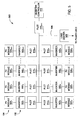
- FIG. 1 is a block diagram of a system 100 for communicating data over an AC power line in accordance with one or more embodiments of the present invention.
- the system 100 comprises a device 102 coupled to a power line communications transceiver (PLCT) 104, which is further coupled to an AC power line 120 ("power line 120") via a junction box 114.
- the system 100 comprises a device 102A coupled to a PLCT 104A, which is further coupled to the power line 120 via a junction box 114A.
- the devices 102 and 102A are devices requiring communications bandwidth for transmitting and/or receiving data, such as a home computer, peripheral device, and the like, and are capable of communicating with one another over the power line 120 via the PLCTs 104 and 104A, respectively.
- the PLCT 104 and/or the PLCT 104A may be coupled directly to the power line 120 without the use of junction boxes 114/114A.
- One particular embodiment that uses the inventive system is described below with respect to Figure 5 .
- the PLCT 104 comprises a transmitter 106 and a receiver 108, each coupled to the device 102, and a coupler 110 that couples both the transmitter 106 and the receiver 108 to the junction box 114.
- the transmitter 106 is capable of transmitting data to the device 102A via the power line 120.
- the receiver 108 is capable of receiving data from the device 102A via the power line 120.
- the PLCT 104 may be able to simultaneously receive and transmit data; however, the transmitter 106 may generally blind the receiver 108 while active.
- a controller 116 is coupled to the transmitter 106 and provides a control signal for enabling and disabling the transmit mode.
- the controller 116 may be separate from the PLCT 104 as depicted in Figure 1 , or, alternatively, the controller 116 may be a component of the PLCT 104.
- the PLCT 104A comprises a transmitter 106A, a receiver 108A, and a coupler 110A.
- the transmitter 106A and receiver 108A are coupled to the device 102A as well as the coupler 110A, and the coupler 110A is further coupled to the junction box 114A.
- the transmitter 106A is capable of transmitting data to the device 102 via the power line 120.
- the receiver 108A is capable of receiving data from the device 102 via the power line 120.
- the PLCT 104A may be able to simultaneously receive and transmit data; however, the transmitter 106A may generally blind the receiver 108A while active.
- a controller 116A is coupled to the transmitter 106A and provides a control signal for enabling and disabling the transmit mode.
- the controller 116A may be separate from the PLCT 104A as depicted in Figure 1 , or, alternatively, the controller 116A may be a component of the PLCT 104A.
- the transmitter 106 when operating in the transmit mode the transmitter 106 receives digital input data from the device 102 and digitally processes the received data through a voltage amplification stage to generate digitally processed data. Following the voltage amplification stage, the transmitter 106 generates an analog voltage waveform for transmitting the digitally processed data over the power line 120 such that the analog voltage waveform characteristics (e.g., frequency, magnitude, spectral purity, and the like) meet relevant standards for PLC.
- analog voltage waveform characteristics e.g., frequency, magnitude, spectral purity, and the like
- the analog voltage waveform may be generated to have a frequency within the band 50-500 KHz (for example, in the 95-148KHz band) and a maximum voltage on the order of 1 volt root mean square (RMS), i.e., 120 decibel/microvolt (dB ⁇ V).
- RMS root mean square
- the coupler 110 couples the generated analog voltage waveform to the power line 120.
- the transmitter 106 During the transmit mode, the transmitter 106 presents a minimal impedance (e.g., within a range of 1-5 ohms) to the power line 120.
- the transmitter 106 In order to meet required output voltage levels given the variability of impedance on the power line 120, the transmitter 106 is capable of driving large currents, for example on the order of hundreds of milliamperes, on the power line 120.
- the transmitter 106 may employ a high-current rated complementary metal-oxide-semiconductor (CMOS) buffer, as described further below, for performing the voltage amplification in the digital domain and driving the necessary current levels.
- CMOS complementary metal-oxide-semiconductor
- the coupler 110 couples an analog signal from the power line 120 to the receiver 108.
- the receiver 108 converts the received analog voltage waveform to digital output data and provides the digital output data to the device 102.
- the digital output data may be a digital representation of a modulated signal; for example, the digital output data may be a digital representation of an FSK signal (a digital FSK signal), and an FSK demodulator is contained within the device 102 or coupled between the receiver 108 and the device 102.
- the receiver 108 as further described below, may comprise a band-pass filter for filtering the received waveform to remove noise inherent to the power line 120.
- the PLCT 104 When the transmit mode is disabled, the PLCT 104 presents a large input impedance to the power line 120 (e.g., on the order of kilo-ohms). Such a large input impedance prevents the transmitter 106 from being “swamped out” when a large number of nodes are present on the power line 120.
- the PLCT 104 comprises only the transmitter 106 and the coupler 110 for transmitting information via the power line 120; additionally or alternatively, the PLCT 104A may comprise only the transmitter 106A and the coupler 110A for transmitting information via the power line 120.
- the receivers 108 and/or 108A are not used. The optional nature of including a receiver is represented by the dashed boxes of receivers 108 and 108A.
- FIG. 2 is a block diagram of a transmitter 106 in accordance with one or more embodiments of the present invention.
- the transmitter 106 comprises a frequency control generator 202 coupled to a direct digital synthesizer (DDS) 204, which is further coupled to a delta-sigma ( ⁇ ) modulator 206.
- DDS direct digital synthesizer
- ⁇ delta-sigma
- the ⁇ modulator 206 is coupled to a CMOS buffer 208, and an output from the CMOS buffer 208 is coupled to a low-pass filter 210.
- the CMOS buffer 208 is additionally coupled to the controller 116 for receiving an input to enable/disable the transmit mode.
- the CMOS buffer 208 When the transmit mode is enabled, the CMOS buffer 208 presents a low transmit impedance (e.g., on the order of 1-5 ohms); when the transmit mode is disabled, the CMOS buffer 208 presents a large input impedance (e.g., on the order of kilo-ohms).
- the frequency control generator 202 is coupled to the device 102 for receiving a digital input data signal for transmission over the power line 120.
- the frequency control generator 202 generates a digital frequency control signal (for example, a 16 to 24 bit signal) based on the received data signal and couples the digital frequency control signal to the DDS 204.
- the DDS 204 operates at a high frequency and, in accordance with the frequency control signal, generates a digital frequency-shift keying (FSK) signal (i.e., a digital representation of an FSK signal).
- the digital FSK signal may be on the order of 8-10 bits wide at a frequency of 25 MHz; alternatively, the digital FSK signal may comprise fewer or more bits and/or may be at a different frequency.
- minimum FSK modulation may be utilized; in some other alternative embodiments, modulation techniques other than FSK modulation may be utilized, such as M-ary quadrature amplitude modulation (QAM), quadrature phase-shift keying (QPSK), phase-shift keying (PSK), orthogonal frequency-division multiplexing (OFDM), pulse-amplitude modulation (PAM), or the like.
- QAM quadrature amplitude modulation
- QPSK quadrature phase-shift keying
- PSK phase-shift keying
- OFDM orthogonal frequency-division multiplexing
- PAM pulse-amplitude modulation
- the DDS 204 output signal is coupled to the ⁇ modulator 206, which may be a single-stage ⁇ modulator or a multi-stage ⁇ modulator.
- the ⁇ modulator 206 encodes the received digital FSK signal utilizing pulse-density modulation (PDM) and provides a digital 1-bit output signal representing the received digital FSK signal.
- PDM pulse-density modulation
- the ⁇ modulator 206 may operate at a frequency of 25 MHz; in alternative embodiments, the ⁇ modulator 206 may operate at a different frequency.
- the frequency control generator 202, DD2 204, and ⁇ modulator 206 form a modulator 212 that generates a digital signal based on the digital input data signal from the device 102.
- the digital signal from the modulator 212 i.e., the output of the ⁇ modulator 206 is coupled to the CMOS buffer 208 for amplifying the voltage.
- the CMOS buffer 208 may be a high-current rated CMOS buffer capable of providing sufficient current (e.g., hundreds of milliamperes) to maintain a required output voltage level when the power line impedance is very low; in some embodiments, the CMOS buffer 208 may be on the order of 0.15 to 0.25 micron technology.
- the CMOS buffer 208 may comprise a plurality of buffers (e.g., sixteen buffers) coupled in parallel, each buffer capable of producing current on the order of 50 mA.
- the number of buffers coupled in parallel determines the amount of current that can be driven and is considered a design choice for the system.
- the CMOS buffer 208 produces a digital output signal which is coupled to the low-pass filter 210 and filtered to generate an analog output.
- the low-pass filtering can be performed in the MHz frequency band to remove sufficient artifacts resulting from the ⁇ modulation.
- the output of the low-pass filter 210 is coupled to the power line 120 through the coupler 110, as explained further below with respect to figure 4 .
- FIG. 3 is a block diagram of a receiver 108 in accordance with one or more embodiments of the present invention.
- the receiver 108 receives an analog voltage waveform from the power line 120 through the coupler 110, as further described below, and generates a digital output data signal that is coupled to the device 102.
- the receiver 108 comprises capacitors 302, 304, 306, and 314; an inductor 308; resistors 312 and 310; and an analog-to-digital (A/D) converter 316.
- one or more the capacitors/inductor/resistors may be a parasitic component.
- the capacitors 302, 304, and 306 are coupled in series such that the capacitor 302 is coupled to the capacitor 304 which is in turn coupled to the capacitor 306, and the received analog waveform is coupled from the coupler 110 across the series combination of capacitors 302, 304, and 306.
- the inductor 308 is coupled across the series combination of the capacitors 304 and 306.
- the capacitors 302, 304, and 306 and the inductor 308 perform band-pass filtering of the received analog voltage waveform to reduce noise that is inherently present on the power line 120 (i.e., to pass the signal of interest with minimal phase/amplitude distortion).
- the resistor 310 is coupled across the capacitor 306.
- the resistor 312 is coupled between a first terminal of the resistor 310 and a first terminal of the capacitor 314; a second terminal of the resistor 310 is coupled to a second terminal of the capacitor 314.
- the A/D converter 316 is coupled across the capacitor 314 and is further coupled to the device 102.
- the resistors 310 and 312 form a high impedance resistive load, and the A/D converter 316 samples the voltage across this load to produce an FSK-modulated digital output signal for the device 102 (i.e., a digital representation of an FSK signal).
- the device 102 comprises an FSK demodulator for demodulating the digital output signal; alternatively, an FSK demodulator may be coupled between the receiver 108 and the device 102.
- the digital output data signal may be a digital representation of a minimum FSK modulated signal, a QAM modulated signal, a QPSK modulated signal, a PSK modulated signal, an OFDM modulated signal, a PAM modulated signal, or the like.
- the resistors 310 and 312 may each be on the order of a few hundred ohms; the capacitors 304, 306, and 314 may each be on the order of a few nanofarads; the capacitor 3.02 may be on the order of several hundred picofarads; and the inductor 308 may be on the order of a few hundred microhenries.
- FIG. 4 is a block diagram of a coupler 110 in accordance with one or more embodiments of the present invention.
- the coupler 110 comprises a transformer 402, an inductor 404 to represent a leakage inductance of the transformer 402, a resistor 406, and capacitors 408 and 410.
- the coupler 110 may be simplified.
- the transmit signal must be low pass filtered without increasing the output impedance and loading the receiver while inactive; the receive signal must be band pass filtered to pass the signal of interest and attenuate out of band noise, while maintaining high impedance in the band of interest.
- the transformer 402 is an isolation transformer having a high coupling factor; for example, the coupling factor may be 0.95 or greater. Generally, the transformer 402 has a 1:1 turns ratio, although other turns ratios may also be utilized.
- a primary winding of the transformer 402 is coupled across each of the transmitter 106 and the receiver 108.
- a first terminal of a secondary winding of the transformer 402 is depicted as coupled to a first terminal of the inductor 404.
- the resistor 406 is coupled between a second terminal of the inductor 404 and a first terminal of the capacitor 408, which provides a safety function for coupling to the power line 120.
- the resistor 406 acts to damp an RLC tank formed by the resistor 406, the inductor 404, and the capacitor 408.
- the capacitor 410 is coupled between a second terminal of the capacitor 408 and a second terminal of the secondary winding of the transformer 402, and is further coupled across two output terminals of the coupler 110 for coupling to the power line 120 through the junction box 114.
- the capacitor 410 provides an optional low-pass filtering function; in some alternative embodiments, the capacitor 410 may be removed from the coupler 110.
- the coupler 110 couples the outbound analog voltage waveform from the transmitter 106 to the power line 120 and couples the inbound analog voltage waveform from the power line 120 to the receiver 108.
- the primary and secondary windings of the transformer 402 each have an inductance on the order of a few hundred microhenries; the inductor 404 (i.e., the leakage inductance of the transformer 402) is on the order of a few microhenries; the resistor 406 is on the order of a few ohms; the capacitor 408 is on the order of a few hundred nanofarads; and the capacitor 410 is on the order of a few nanofarads.
- Figure 5 is a block diagram of a system 500 for inverting solar generated DC power to AC power using one or more embodiments of the present invention. This diagram only portrays one variation of the myriad of possible system configurations and devices that may utilize the present invention.
- the present invention can be utilized by any device for power line communication, and can function in a variety of distributed environments and systems requiring communications over power lines.
- the system 500 comprises a plurality of inverters 502 1 , 502 2 ... 502 n , collectively referred to as inverters 502, a plurality of PV modules 504 1 , 504 2 ... 504 n , collectively referred to as PV modules 504, a plurality of PLCTs 512 1 , 512 2 ... 512 n , 512 n+1 , collectively referred to as PLCTs 512, AC power line 506, an inverter controller 510, and a load center 508.
- Each inverter 502 1 , 502 2 ... 502 n is coupled to a PLCT 512 1 , 512 2 ... 512 n , respectively; in some alternative embodiments, each of the PLCTs 512 1 , 512 2 ... 512 n may be contained within the corresponding inverter 502 1 , 502 2 ... 502 n .
- Each inverter 502 1 , 502 2 ... 502 n is additionally coupled to a PV module 504 1 ,...504 2 . .. 504 n , respectively.
- the inverter controller 510 is coupled to the PLCT 512 n+1 .
- the PLCTs 512 are coupled to the AC power line 506 and operate analogously to the PLCTs 104 and 104A described above.
- each of the PLCTs 512 may be coupled to a controller (i.e., one controller per PLCT 512), such as controller 116, for enabling/disabling a transmit mode of the PLCT 512.
- the AC power line 506 is further coupled to the load center 508 which houses connections between incoming commercial AC power lines from a commercial AC power grid distribution system and the AC power line 506.
- the inverters 502 convert DC power generated by the PV modules 504 into AC power, and meter out AC current that is in-phase with the commercial AC power grid voltage.
- the system 500 couples the generated AC power to the commercial AC power grid via the load center 508.
- the inverter controller 510 is capable of receiving data from the inverters 502 and issuing command and control signals to the inverters 502 for controlling the functionality of the inverters 502.
- the PLCTs 512 enable such communication between the inverters 502 and the inverter controller 510 over the AC power lines 506.
- the PLCTs 512 digitally process digital input data from the inverters 502 and/or the inverter controller 510 through a voltage amplification stage and generate a corresponding analog voltage waveform that is coupled to the AC power lines 506 for transmitting the received digital input data.
- the PLCTs 512 receive an analog voltage waveform from the AC power line 506 and process the received waveform to produce digital output data that is coupled to the inverters 502 and/or the inverter controller 510, thereby allowing the inverters 501 and the inverter controller 510 to communicate over the AC power lines 506.
Description
- Embodiments of the present disclosure relate generally to power line communications and, more particularly, to an apparatus for providing communication over power lines.
- Power Line Communications (PLC) is a technology for utilizing power lines, such as the existing commercial AC power grid infrastructure, to communicate data between devices coupled to the power lines. PLC typically operates in a point-to-multipoint fashion where one transmitter at a time transmits over the power line while other devices coupled to the power line receive the transmitted signal.
- For PLC transmission, a transmitter is generally coupled to the power line through an isolation transformer and sends a voltage stimulus on the power line (i.e., a voltage-based signal) in accordance with relevant standards for PLC, such as BS EN 50065-1:2001 "Specification for Signaling on Low-Voltage Electrical Installations in the Frequency Range 3 kHz to 148.5 kHz". These relevant standards set forth specifications for PLC operation, such as a maximum voltage level. As a result of power lines having undefined and variable impedances within the frequency band of interest for PLC, a transmitter module may be required to generate a large amount of current, for example on the order of hundreds of milliamperes, in order to meet the PLC voltage requirements.
- Document Motorola & Freescale semiconductor Inc. "Power line modem reference design", March 1, 2013, refers to a power line modem. Both frequency shift keying modulation / demodulation routines are fully handled by a digital signal processor. Capacitors and filters are provided for filtering and coupling. Document
US 5,404, 127 describes a power line communication (PLC) apparatus wherein a carrier is derived to avoid determinable interference harmonics. In order to transmit data on a power line containing the television interference or other determinable interference harmonics, redundant carriers at a frequency between the television interference harmonics is used. A waveshaping and modulation circuit for generating the modulated data waveform for output over the power line is used. The waveshaping and modulation circuit can include a waveshape ROM for storing samples that represent the appearance of the carrier waveshape. DocumentUS 2007/152628 describes an AC/DC power device for AC/DC power line communication. An AC/DC protection circuit coupled to an AC/DC power line is able to receive an AC or DC power. An AC/DC configuration circuit coupled to the AC/DC protection circuit is used to switch between an AC mode and a DC mode PLC. An AC/DC coupling/filtering circuit coupled to the AC/DC configuration circuit is to couple and filter the received power, and then coupled an AC voltage or a first DC voltage. An AC/DC converter coupled to the AC/DC coupling/filtering circuit is used to convert the AC voltage into a second DC voltage. A DC/DC converter coupled to the AC/DC coupling/filtering circuit and the AC/DC converter is to convert the first DC voltage (DC mode) and convert the second DC voltage (AC mode), so as to output DC voltages respectively to analog and digital circuit of the PLC modern. - Generally, PLC transmitters use linear amplifiers to achieve the required amplification and signal processing for PLC transmission. However, such devices dissipate high levels of power when operating to drive large currents on the power line and thus decrease the efficiency of the PLC transmitters. Additionally, the PLC transmitters generally perform filtering prior to the power amplification in order to satisfy spectral purity requirements set forth in the relevant standards, requiring a large number of costly components.
- For receiving data transmitted over the power line, a PLC receiver is typically also coupled to the power line through an isolation transformer. The PLC receiver is required to provide a large input impedance to limit noise from the power line into the receiver prior to amplification, thereby requiring a costly number of components to perform such functions.
- Therefore, there is a need in the art for an apparatus for efficient power line communications.
- Embodiments of the present invention generally relate to an apparatus and system for communicating data via a power line. The apparatus comprises a transmitter comprising a modulator for generating a second digital signal based on input data, wherein the modulator comprises a direct digital synthesizer for generating a first digital signal based on the input data and a delta-sigma modulator for generating the second digital signal based on the first digital signal; a digital buffer for amplifying the second digital signal to generate a third digital signal wherein the digital buffer receives a control signal for enabling a transmit mode; a filter for filtering the third digital signal to generate an analog output waveform; and a coupler for coupling the analog output waveform to the power line.
- So that the manner in which the above recited features of the present invention can be understood in detail, a more particular description of the invention, briefly summarized above, may be had by reference to embodiments, some of which are illustrated in the appended drawings. It is to be noted, however, that the appended drawings illustrate only typical embodiments of this invention and are therefore not to be considered limiting of its scope, for the invention may admit to other equally effective embodiments.
-
Figure 1 is a block diagram of a system for communicating data over an AC power line in accordance with one or more embodiments of the present invention; -
Figure 2 is a block diagram of a transmitter in accordance with one or more embodiments of the present invention; -
Figure 3 is a block diagram of a receiver in accordance with one or more embodiments of the present invention; -
Figure 4 is a block diagram of a coupler in accordance with one or more embodiments of the present invention; and -
Figure 5 is a block diagram of a system for inverting solar generated DC power to AC power using one or more embodiments of the present invention. -
Figure 1 is a block diagram of asystem 100 for communicating data over an AC power line in accordance with one or more embodiments of the present invention. Thesystem 100 comprises adevice 102 coupled to a power line communications transceiver (PLCT) 104, which is further coupled to an AC power line 120 ("power line 120") via ajunction box 114. Additionally, thesystem 100 comprises adevice 102A coupled to aPLCT 104A, which is further coupled to thepower line 120 via ajunction box 114A. Thedevices power line 120 via thePLCTs PLCT 104 and/or the PLCT 104A may be coupled directly to thepower line 120 without the use ofjunction boxes 114/114A. One particular embodiment that uses the inventive system is described below with respect toFigure 5 . - The
PLCT 104 comprises atransmitter 106 and areceiver 108, each coupled to thedevice 102, and acoupler 110 that couples both thetransmitter 106 and thereceiver 108 to thejunction box 114. When the PLCT 104 is operating in a "transmit mode", thetransmitter 106 is capable of transmitting data to thedevice 102A via thepower line 120. Thereceiver 108 is capable of receiving data from thedevice 102A via thepower line 120. The PLCT 104 may be able to simultaneously receive and transmit data; however, thetransmitter 106 may generally blind thereceiver 108 while active. In some embodiments, acontroller 116 is coupled to thetransmitter 106 and provides a control signal for enabling and disabling the transmit mode. Thecontroller 116 may be separate from thePLCT 104 as depicted inFigure 1 , or, alternatively, thecontroller 116 may be a component of thePLCT 104. - Analogous to the
PLCT 104, thePLCT 104A comprises atransmitter 106A, areceiver 108A, and acoupler 110A. Thetransmitter 106A andreceiver 108A are coupled to thedevice 102A as well as thecoupler 110A, and thecoupler 110A is further coupled to thejunction box 114A. When the PLCT 104A is operating in a transmit mode, thetransmitter 106A is capable of transmitting data to thedevice 102 via thepower line 120. Thereceiver 108A is capable of receiving data from thedevice 102 via thepower line 120. The PLCT 104A may be able to simultaneously receive and transmit data; however, thetransmitter 106A may generally blind thereceiver 108A while active. In some embodiments, acontroller 116A is coupled to thetransmitter 106A and provides a control signal for enabling and disabling the transmit mode. Thecontroller 116A may be separate from thePLCT 104A as depicted inFigure 1 , or, alternatively, thecontroller 116A may be a component of thePLCT 104A. - In accordance with one or more embodiments of the present invention, when operating in the transmit mode the
transmitter 106 receives digital input data from thedevice 102 and digitally processes the received data through a voltage amplification stage to generate digitally processed data. Following the voltage amplification stage, thetransmitter 106 generates an analog voltage waveform for transmitting the digitally processed data over thepower line 120 such that the analog voltage waveform characteristics (e.g., frequency, magnitude, spectral purity, and the like) meet relevant standards for PLC. In some embodiments, the analog voltage waveform may be generated to have a frequency within the band 50-500 KHz (for example, in the 95-148KHz band) and a maximum voltage on the order of 1 volt root mean square (RMS), i.e., 120 decibel/microvolt (dBµV). Thecoupler 110 couples the generated analog voltage waveform to thepower line 120. - During the transmit mode, the
transmitter 106 presents a minimal impedance (e.g., within a range of 1-5 ohms) to thepower line 120. In order to meet required output voltage levels given the variability of impedance on thepower line 120, thetransmitter 106 is capable of driving large currents, for example on the order of hundreds of milliamperes, on thepower line 120. In order to drive such large currents, thetransmitter 106 may employ a high-current rated complementary metal-oxide-semiconductor (CMOS) buffer, as described further below, for performing the voltage amplification in the digital domain and driving the necessary current levels. - When the
PLCT 104 is receiving, thecoupler 110 couples an analog signal from thepower line 120 to thereceiver 108. Thereceiver 108 converts the received analog voltage waveform to digital output data and provides the digital output data to thedevice 102. In some embodiments, the digital output data may be a digital representation of a modulated signal; for example, the digital output data may be a digital representation of an FSK signal (a digital FSK signal), and an FSK demodulator is contained within thedevice 102 or coupled between thereceiver 108 and thedevice 102. Thereceiver 108, as further described below, may comprise a band-pass filter for filtering the received waveform to remove noise inherent to thepower line 120. When the transmit mode is disabled, thePLCT 104 presents a large input impedance to the power line 120 (e.g., on the order of kilo-ohms). Such a large input impedance prevents thetransmitter 106 from being "swamped out" when a large number of nodes are present on thepower line 120. - In some alternative embodiments, the
PLCT 104 comprises only thetransmitter 106 and thecoupler 110 for transmitting information via thepower line 120; additionally or alternatively, thePLCT 104A may comprise only thetransmitter 106A and thecoupler 110A for transmitting information via thepower line 120. In such embodiments, thereceivers 108 and/or 108A are not used. The optional nature of including a receiver is represented by the dashed boxes ofreceivers -
Figure 2 is a block diagram of atransmitter 106 in accordance with one or more embodiments of the present invention. Thetransmitter 106 comprises afrequency control generator 202 coupled to a direct digital synthesizer (DDS) 204, which is further coupled to a delta-sigma (Δ∑)modulator 206. The Δ∑ modulator 206 is coupled to aCMOS buffer 208, and an output from theCMOS buffer 208 is coupled to a low-pass filter 210. TheCMOS buffer 208 is additionally coupled to thecontroller 116 for receiving an input to enable/disable the transmit mode. When the transmit mode is enabled, theCMOS buffer 208 presents a low transmit impedance (e.g., on the order of 1-5 ohms); when the transmit mode is disabled, theCMOS buffer 208 presents a large input impedance (e.g., on the order of kilo-ohms). - The
frequency control generator 202 is coupled to thedevice 102 for receiving a digital input data signal for transmission over thepower line 120. Thefrequency control generator 202 generates a digital frequency control signal (for example, a 16 to 24 bit signal) based on the received data signal and couples the digital frequency control signal to theDDS 204. TheDDS 204 operates at a high frequency and, in accordance with the frequency control signal, generates a digital frequency-shift keying (FSK) signal (i.e., a digital representation of an FSK signal). In some embodiments, the digital FSK signal may be on the order of 8-10 bits wide at a frequency of 25 MHz; alternatively, the digital FSK signal may comprise fewer or more bits and/or may be at a different frequency. In some alternative embodiments, minimum FSK modulation may be utilized; in some other alternative embodiments, modulation techniques other than FSK modulation may be utilized, such as M-ary quadrature amplitude modulation (QAM), quadrature phase-shift keying (QPSK), phase-shift keying (PSK), orthogonal frequency-division multiplexing (OFDM), pulse-amplitude modulation (PAM), or the like. - The
DDS 204 output signal is coupled to the Δ∑ modulator 206, which may be a single-stage Δ∑ modulator or a multi-stage Δ∑ modulator. The Δ∑ modulator 206 encodes the received digital FSK signal utilizing pulse-density modulation (PDM) and provides a digital 1-bit output signal representing the received digital FSK signal. In some embodiments, the Δ∑ modulator 206 may operate at a frequency of 25 MHz; in alternative embodiments, the Δ∑ modulator 206 may operate at a different frequency. - The
frequency control generator 202,DD2 204, and Δ∑ modulator 206 form amodulator 212 that generates a digital signal based on the digital input data signal from thedevice 102. The digital signal from the modulator 212 (i.e., the output of the Δ∑ modulator 206) is coupled to theCMOS buffer 208 for amplifying the voltage. TheCMOS buffer 208 may be a high-current rated CMOS buffer capable of providing sufficient current (e.g., hundreds of milliamperes) to maintain a required output voltage level when the power line impedance is very low; in some embodiments, theCMOS buffer 208 may be on the order of 0.15 to 0.25 micron technology. In some embodiments, theCMOS buffer 208 may comprise a plurality of buffers (e.g., sixteen buffers) coupled in parallel, each buffer capable of producing current on the order of 50 mA. The number of buffers coupled in parallel determines the amount of current that can be driven and is considered a design choice for the system. - Following the voltage amplification, the
CMOS buffer 208 produces a digital output signal which is coupled to the low-pass filter 210 and filtered to generate an analog output. As a result of the Δ∑ modulator 206 running at a high frequency, for example 25 MHz, the low-pass filtering can be performed in the MHz frequency band to remove sufficient artifacts resulting from the Δ∑ modulation. The output of the low-pass filter 210 is coupled to thepower line 120 through thecoupler 110, as explained further below with respect tofigure 4 . -
Figure 3 is a block diagram of areceiver 108 in accordance with one or more embodiments of the present invention. Thereceiver 108 receives an analog voltage waveform from thepower line 120 through thecoupler 110, as further described below, and generates a digital output data signal that is coupled to thedevice 102. - The
receiver 108 comprisescapacitors inductor 308;resistors converter 316. In some embodiments, one or more the capacitors/inductor/resistors may be a parasitic component. Thecapacitors capacitor 302 is coupled to thecapacitor 304 which is in turn coupled to thecapacitor 306, and the received analog waveform is coupled from thecoupler 110 across the series combination ofcapacitors inductor 308 is coupled across the series combination of thecapacitors capacitors inductor 308 perform band-pass filtering of the received analog voltage waveform to reduce noise that is inherently present on the power line 120 (i.e., to pass the signal of interest with minimal phase/amplitude distortion). - The
resistor 310 is coupled across thecapacitor 306. Theresistor 312 is coupled between a first terminal of theresistor 310 and a first terminal of thecapacitor 314; a second terminal of theresistor 310 is coupled to a second terminal of thecapacitor 314. The A/D converter 316 is coupled across thecapacitor 314 and is further coupled to thedevice 102. Theresistors D converter 316 samples the voltage across this load to produce an FSK-modulated digital output signal for the device 102 (i.e., a digital representation of an FSK signal). In some embodiments, thedevice 102 comprises an FSK demodulator for demodulating the digital output signal; alternatively, an FSK demodulator may be coupled between thereceiver 108 and thedevice 102. In some alternative embodiments, the digital output data signal may be a digital representation of a minimum FSK modulated signal, a QAM modulated signal, a QPSK modulated signal, a PSK modulated signal, an OFDM modulated signal, a PAM modulated signal, or the like. - In some embodiments, the
resistors capacitors inductor 308 may be on the order of a few hundred microhenries. -
Figure 4 is a block diagram of acoupler 110 in accordance with one or more embodiments of the present invention. Thecoupler 110 comprises atransformer 402, aninductor 404 to represent a leakage inductance of thetransformer 402, aresistor 406, andcapacitors coupler 110 may be simplified. Generally, the transmit signal must be low pass filtered without increasing the output impedance and loading the receiver while inactive; the receive signal must be band pass filtered to pass the signal of interest and attenuate out of band noise, while maintaining high impedance in the band of interest. - The
transformer 402 is an isolation transformer having a high coupling factor; for example, the coupling factor may be 0.95 or greater. Generally, thetransformer 402 has a 1:1 turns ratio, although other turns ratios may also be utilized. A primary winding of thetransformer 402 is coupled across each of thetransmitter 106 and thereceiver 108. A first terminal of a secondary winding of thetransformer 402 is depicted as coupled to a first terminal of theinductor 404. Theresistor 406 is coupled between a second terminal of theinductor 404 and a first terminal of thecapacitor 408, which provides a safety function for coupling to thepower line 120. Theresistor 406 acts to damp an RLC tank formed by theresistor 406, theinductor 404, and thecapacitor 408. - The
capacitor 410 is coupled between a second terminal of thecapacitor 408 and a second terminal of the secondary winding of thetransformer 402, and is further coupled across two output terminals of thecoupler 110 for coupling to thepower line 120 through thejunction box 114. Thecapacitor 410 provides an optional low-pass filtering function; in some alternative embodiments, thecapacitor 410 may be removed from thecoupler 110. - The
coupler 110 couples the outbound analog voltage waveform from thetransmitter 106 to thepower line 120 and couples the inbound analog voltage waveform from thepower line 120 to thereceiver 108. - In some embodiments, the primary and secondary windings of the
transformer 402 each have an inductance on the order of a few hundred microhenries; the inductor 404 (i.e., the leakage inductance of the transformer 402) is on the order of a few microhenries; theresistor 406 is on the order of a few ohms; thecapacitor 408 is on the order of a few hundred nanofarads; and thecapacitor 410 is on the order of a few nanofarads. -
Figure 5 is a block diagram of asystem 500 for inverting solar generated DC power to AC power using one or more embodiments of the present invention. This diagram only portrays one variation of the myriad of possible system configurations and devices that may utilize the present invention. The present invention can be utilized by any device for power line communication, and can function in a variety of distributed environments and systems requiring communications over power lines. - The
system 500 comprises a plurality ofinverters inverters 502, a plurality ofPV modules PV modules 504, a plurality of PLCTs 5121, 5122 ... 512n, 512n+1, collectively referred to as PLCTs 512,AC power line 506, aninverter controller 510, and aload center 508. - Each
inverter inverter inverter PV module 5041,...5042. .. 504n, respectively. Theinverter controller 510 is coupled to the PLCT 512n+1. - The PLCTs 512 are coupled to the
AC power line 506 and operate analogously to thePLCTs controller 116, for enabling/disabling a transmit mode of the PLCT 512. TheAC power line 506 is further coupled to theload center 508 which houses connections between incoming commercial AC power lines from a commercial AC power grid distribution system and theAC power line 506. Theinverters 502 convert DC power generated by thePV modules 504 into AC power, and meter out AC current that is in-phase with the commercial AC power grid voltage. Thesystem 500 couples the generated AC power to the commercial AC power grid via theload center 508. - The
inverter controller 510 is capable of receiving data from theinverters 502 and issuing command and control signals to theinverters 502 for controlling the functionality of theinverters 502. In accordance with one or more embodiments of the present invention, the PLCTs 512 enable such communication between theinverters 502 and theinverter controller 510 over theAC power lines 506. As previously described, the PLCTs 512 digitally process digital input data from theinverters 502 and/or theinverter controller 510 through a voltage amplification stage and generate a corresponding analog voltage waveform that is coupled to theAC power lines 506 for transmitting the received digital input data. Also, as previously described, the PLCTs 512 receive an analog voltage waveform from theAC power line 506 and process the received waveform to produce digital output data that is coupled to theinverters 502 and/or theinverter controller 510, thereby allowing the inverters 501 and theinverter controller 510 to communicate over theAC power lines 506. - While the foregoing is directed to embodiments of the present invention, other and further embodiments of the invention may be devised without departing from the basic scope thereof, and the scope thereof is determined by the claims that follow.
Claims (10)
- Apparatus for communicating via a power line, comprising:a transmitter (106, 106A) comprising a modulator (212) for generating a second digital signal based on input data, wherein the modulator (212) comprises a direct digital synthesizer for generating a first digital signal based on the input data and a delta-sigma modulator (206) for generating the second digital signal based on the first digital signal;a digital buffer (208) for amplifying the second digital signal to generate a third digital signal, wherein the digital buffer (208) receives a control signal for enabling a transmit mode;a filter (210) for filtering the third digital signal to generate an analog output waveform; anda coupler (110, 110A) for coupling the analog output waveform to the power line.
- The apparatus of claim 1, wherein the first digital signal is a digital frequency shift keying (FSK) signal and the second digital signal is a pulse density modulated (PDM) signal.
- The apparatus of claim 1, wherein the digital buffer (106, 106A) presets a minimal impedance during the transmit mode, such that the transmitter (106, 106A) presents a minimal impedance to the power line.
- The apparatus of claim 1, further comprising a receiver (108, 108A) for receiving an analog input waveform from the power line via the coupler (110, 110A) and generating a digital output signal based on the analog input waveform.
- The apparatus of claim 4, wherein the receiver (108, 108A) is capable of receiving the analog waveform when the transmit mode is disabled.
- The apparatus of claim 5, wherein the digital buffer (208) presents a higher impedance when the transmit mode is disabled than when the transmit mode is enabled.
- The apparatus of claim 1, wherein the coupler (110, 110A) comprises a transformer, a resistor, a first capacitor and a second capacitor, wherein a primary winding of the transformer is coupled across an output of the transmitter (106, 106A); a secondary winding of the transformer is coupled across a series combination of the resistor, the first and the second capacitors, and an output of the coupler is coupled across the second capacitor.
- The apparatus of claim 4, wherein the receiver (108, 108A) comprises an analog to digital (A/D) converter, a first capacitor, a second capacitor, a third capacitor, a fourth capacitor, a first resistor, a second resistor, and an inductor; wherein the A/D converter is coupled across the first capacitor; a first terminal of the first resistor is coupled to a first terminal of the first capacitor and a second terminal of the first resistor is coupled to a first terminal of the second resistor, a first terminal of the second capacitor, and a first terminal of the third capacitor; a second terminal of the third capacitor is coupled to a first terminal of the fourth capacitor and a first terminal of the inductor; a second terminal of the inductor is coupled to a second terminal of the second capacitor, a second terminal of the second resistor, and a second terminal of the first capacitor; and an input to the receiver is coupled across a second terminal of the fourth capacitor and a second terminal of the inductor.
- The apparatus of any of claims 1-8, further comprising an inverter, wherein the inverter provides the input data.
- The apparatus of any of claims 1-8, further comprising an inverter, wherein the inverter comprises the transmitter (106, 106A), the digital buffer, the filter (210), and the coupler (110, 110A).
Applications Claiming Priority (2)
| Application Number | Priority Date | Filing Date | Title |
|---|---|---|---|
| US27535009P | 2009-08-28 | 2009-08-28 | |
| PCT/US2010/046942 WO2011025934A2 (en) | 2009-08-28 | 2010-08-27 | Power line communications apparatus |
Publications (3)
| Publication Number | Publication Date |
|---|---|
| EP2471190A2 EP2471190A2 (en) | 2012-07-04 |
| EP2471190A4 EP2471190A4 (en) | 2013-08-07 |
| EP2471190B1 true EP2471190B1 (en) | 2015-05-27 |
Family
ID=43624870
Family Applications (1)
| Application Number | Title | Priority Date | Filing Date |
|---|---|---|---|
| EP10812652.5A Active EP2471190B1 (en) | 2009-08-28 | 2010-08-27 | Power line communications apparatus |
Country Status (9)
| Country | Link |
|---|---|
| US (3) | US8107516B2 (en) |
| EP (1) | EP2471190B1 (en) |
| JP (2) | JP5562422B2 (en) |
| KR (1) | KR101664274B1 (en) |
| CN (1) | CN102474303B (en) |
| AU (1) | AU2010286576B2 (en) |
| CA (1) | CA2772573A1 (en) |
| IL (1) | IL218371A0 (en) |
| WO (1) | WO2011025934A2 (en) |
Families Citing this family (43)
| Publication number | Priority date | Publication date | Assignee | Title |
|---|---|---|---|---|
| US7994657B2 (en) * | 2006-12-22 | 2011-08-09 | Solarbridge Technologies, Inc. | Modular system for unattended energy generation and storage |
| US7755916B2 (en) | 2007-10-11 | 2010-07-13 | Solarbridge Technologies, Inc. | Methods for minimizing double-frequency ripple power in single-phase power conditioners |
| US8279642B2 (en) | 2009-07-31 | 2012-10-02 | Solarbridge Technologies, Inc. | Apparatus for converting direct current to alternating current using an active filter to reduce double-frequency ripple power of bus waveform |
| US8462518B2 (en) | 2009-10-12 | 2013-06-11 | Solarbridge Technologies, Inc. | Power inverter docking system for photovoltaic modules |
| US20110122322A1 (en) * | 2009-11-23 | 2011-05-26 | Woo Yeun Kim | Method and apparatus for transmission and reception using power line |
| US8824178B1 (en) | 2009-12-31 | 2014-09-02 | Solarbridge Technologies, Inc. | Parallel power converter topology |
| US20120064851A1 (en) * | 2010-09-10 | 2012-03-15 | Gary Wang | Wireless signal conversion system |
| US8503200B2 (en) | 2010-10-11 | 2013-08-06 | Solarbridge Technologies, Inc. | Quadrature-corrected feedforward control apparatus and method for DC-AC power conversion |
| US8279649B2 (en) | 2010-10-11 | 2012-10-02 | Solarbridge Technologies, Inc. | Apparatus and method for controlling a power inverter |
| US9160408B2 (en) | 2010-10-11 | 2015-10-13 | Sunpower Corporation | System and method for establishing communication with an array of inverters |
| US9467063B2 (en) | 2010-11-29 | 2016-10-11 | Sunpower Corporation | Technologies for interleaved control of an inverter array |
| US8842454B2 (en) | 2010-11-29 | 2014-09-23 | Solarbridge Technologies, Inc. | Inverter array with localized inverter control |
| JP5950944B2 (en) | 2011-02-10 | 2016-07-13 | シェフラー テクノロジーズ アー・ゲー ウント コー. カー・ゲーSchaeffler Technologies AG & Co. KG | Reluctance motor |
| JP5742357B2 (en) * | 2011-03-25 | 2015-07-01 | 住友電気工業株式会社 | Monitoring system for photovoltaic power generation |
| US9065354B2 (en) | 2011-04-27 | 2015-06-23 | Sunpower Corporation | Multi-stage power inverter for power bus communication |
| US8599587B2 (en) | 2011-04-27 | 2013-12-03 | Solarbridge Technologies, Inc. | Modular photovoltaic power supply assembly |
| US8611107B2 (en) | 2011-04-27 | 2013-12-17 | Solarbridge Technologies, Inc. | Method and system for controlling a multi-stage power inverter |
| US8699586B2 (en) * | 2011-06-10 | 2014-04-15 | Didier Boivin | Powerline control interface in CENELEC (EU) A-D bands frequency and amplitude modulation transmitter |
| US8922185B2 (en) | 2011-07-11 | 2014-12-30 | Solarbridge Technologies, Inc. | Device and method for global maximum power point tracking |
| US8716882B2 (en) | 2011-07-28 | 2014-05-06 | Powerline Load Control Llc | Powerline communicated load control |
| US8284574B2 (en) | 2011-10-17 | 2012-10-09 | Solarbridge Technologies, Inc. | Method and apparatus for controlling an inverter using pulse mode control |
| US8958487B2 (en) | 2011-12-22 | 2015-02-17 | Landis+Gyr Technologies, Llc | Power line communication transmitter with amplifier circuit |
| US8847834B2 (en) * | 2012-05-14 | 2014-09-30 | Tag-Comm Inc. | Method and apparatus for generating dedicated data channels in backscatter RFID systems using band-pass modulation |
| US9276635B2 (en) | 2012-06-29 | 2016-03-01 | Sunpower Corporation | Device, system, and method for communicating with a power inverter using power line communications |
| US9654176B2 (en) * | 2013-03-14 | 2017-05-16 | Hiq Solar, Inc. | Measurement, control and harvest optimization device for solar modules requiring fewer connections |
| US9564835B2 (en) | 2013-03-15 | 2017-02-07 | Sunpower Corporation | Inverter communications using output signal |
| US9584044B2 (en) | 2013-03-15 | 2017-02-28 | Sunpower Corporation | Technologies for converter topologies |
| KR20140123854A (en) * | 2013-04-15 | 2014-10-23 | 한국전자통신연구원 | Apparatus and Method for Serial-Connected Power Line Communication |
| TWI543552B (en) | 2013-09-13 | 2016-07-21 | Radiant Opto Electronics Corp | Adaptive control method and system |
| US10135247B2 (en) | 2013-10-17 | 2018-11-20 | General Electric Company | Methods and systems for integrated Volt/VAr control in electric network |
| EP2866354B1 (en) * | 2013-10-25 | 2019-06-26 | VITO NV (Vlaamse Instelling voor Technologisch Onderzoek NV) | Method and system for providing pulsed power and data on a bus |
| CN104955087B (en) | 2014-03-25 | 2019-03-01 | 华为技术有限公司 | A kind of control system and method, relevant device of wireless base station |
| US9148320B1 (en) * | 2014-09-29 | 2015-09-29 | Landis+Gyr Technologies, Llc | Transceiver front-end for communication over power lines |
| CN107408820A (en) | 2014-12-16 | 2017-11-28 | Abb瑞士股份有限公司 | Energy plate arranges power dissipation |
| CN107431097B (en) | 2015-01-28 | 2020-02-14 | Abb瑞士股份有限公司 | Energy panel arrangement closure |
| US10404060B2 (en) | 2015-02-22 | 2019-09-03 | Abb Schweiz Ag | Photovoltaic string reverse polarity detection |
| EP3272083A4 (en) | 2015-05-27 | 2018-12-05 | Hewlett-Packard Development Company, L.P. | Recovering independent waveforms from input bitstream data |
| US9397675B1 (en) * | 2015-07-31 | 2016-07-19 | Shure Acquisition Holdings, Inc. | Hybrid frequency synthesizer and method |
| DE102017003660A1 (en) * | 2017-04-13 | 2018-10-18 | Liebherr-Aerospace Lindenberg Gmbh | Electronic assembly for peripheral devices of an aircraft |
| CN109525284B (en) * | 2017-09-18 | 2021-05-14 | 丰郅(上海)新能源科技有限公司 | System integrating high-frequency switching power supply and direct-current voltage converter and communication method |
| CN108352718B (en) * | 2018-02-07 | 2022-02-08 | 深圳市为通博科技有限责任公司 | Charging detection circuit, charging box, communication device of earphone and earphone |
| FR3083939A1 (en) * | 2018-07-13 | 2020-01-17 | Zodiac Aerotechnics | DATA TRANSMISSION SYSTEM |
| KR102064066B1 (en) * | 2018-04-11 | 2020-01-08 | 울산과학기술원 | Power line communication apparatus and method |
Family Cites Families (39)
| Publication number | Priority date | Publication date | Assignee | Title |
|---|---|---|---|---|
| US4992774A (en) | 1989-01-27 | 1991-02-12 | Mccullough Robert K | Method for powering remote visual displays and allowing for data exchange over the same wire pair |
| US5818127A (en) * | 1989-04-28 | 1998-10-06 | Videocom, Inc. | Transmission of FM video signals over various lines |
| US5257006A (en) | 1990-09-21 | 1993-10-26 | Echelon Corporation | Method and apparatus for power line communications |
| WO1992021194A1 (en) | 1991-05-10 | 1992-11-26 | Echelon Corporation | Power line communication while avoiding determinable interference harmonics |
| JPH07123033A (en) * | 1993-10-26 | 1995-05-12 | Mitsubishi Electric Corp | Distribution line carrier transmission reception equipment |
| US5598158A (en) * | 1994-11-02 | 1997-01-28 | Advanced Micro Devices, Inc. | Digital noise shaper circuit |
| US5589830A (en) * | 1994-11-02 | 1996-12-31 | Advanced Micro Devices, Inc. | Stereo audio codec |
| JPH10201105A (en) * | 1997-01-14 | 1998-07-31 | Nissin Electric Co Ltd | Photovoltaic power generation system |
| US5952914A (en) * | 1997-09-10 | 1999-09-14 | At&T Corp. | Power line communication systems |
| JP3312115B2 (en) * | 1998-03-16 | 2002-08-05 | 大崎電気工業株式会社 | Consumer power management system |
| US5982596A (en) * | 1998-05-05 | 1999-11-09 | George Authur Spencer | Load center monitor and digitally enhanced circuit breaker system for monitoring electrical power lines |
| DE19940544A1 (en) | 1999-08-26 | 2001-03-01 | Abb Patent Gmbh | Coupling stage for a data transmission system for low-voltage networks |
| US6686832B2 (en) * | 2000-05-23 | 2004-02-03 | Satius, Inc. | High frequency network multiplexed communications over various lines |
| US6483388B2 (en) * | 2000-06-21 | 2002-11-19 | Research In Motion Limited | Direct digital frequency synthesizer and a hybrid frequency synthesizer combining a direct digital frequency synthesizer and a phase locked loop |
| US20020041228A1 (en) * | 2000-10-10 | 2002-04-11 | George Zhang | Apparatus for power line computer network system |
| JP4401591B2 (en) * | 2001-03-22 | 2010-01-20 | 三菱電機株式会社 | Transmission / reception switching circuit for power line carrier |
| US6741196B2 (en) | 2002-01-04 | 2004-05-25 | Globespan Virata Incorporated | Method and apparatus for a high-drive current digital-to-analog converter |
| US7199699B1 (en) | 2002-02-19 | 2007-04-03 | Current Technologies, Llc | Facilitating communication with power line communication devices |
| RU2239270C1 (en) | 2003-03-31 | 2004-10-27 | Общество с ограниченной ответственностью "Алгоритм" | Device for suppressing radiation induced by transmitting data in power lines |
| US7577695B2 (en) * | 2004-07-22 | 2009-08-18 | Auburn University | High-order delta-sigma noise shaping in direct digital frequency synthesis |
| JP4543817B2 (en) * | 2004-08-13 | 2010-09-15 | パナソニック電工株式会社 | Power line carrier communication equipment |
| JP4123224B2 (en) * | 2004-11-17 | 2008-07-23 | 松下電工株式会社 | Power line carrier communication equipment |
| JP4849872B2 (en) * | 2005-11-04 | 2012-01-11 | パナソニック株式会社 | Electrical device, visible light communication method, and circuit module |
| GB2432982A (en) * | 2005-11-30 | 2007-06-06 | Toshiba Res Europ Ltd | An EER RF amplifier with PWM signal switching |
| JP4344948B2 (en) * | 2005-12-21 | 2009-10-14 | 横河電機株式会社 | DDS circuit |
| TWI289386B (en) | 2005-12-30 | 2007-11-01 | Ind Tech Res Inst | AC/DC power line communication modem |
| US7932790B2 (en) * | 2006-10-27 | 2011-04-26 | Telefonaktiebolaget Lm Ericsson (Publ) | Switched modulation of a radio-frequency amplifier |
| JP2008160490A (en) * | 2006-12-25 | 2008-07-10 | Sharp Corp | Ac adapter for power line communication and information terminal |
| WO2008112080A1 (en) * | 2007-03-07 | 2008-09-18 | Greenray, Inc. | Data acquisition apparatus and methodology for self-diagnosis of ac modules |
| US10468993B2 (en) * | 2007-05-17 | 2019-11-05 | Enphase Energy, Inc. | Inverter for use in photovoltaic module |
| US20090000654A1 (en) * | 2007-05-17 | 2009-01-01 | Larankelo, Inc. | Distributed inverter and intelligent gateway |
| US8724733B2 (en) * | 2007-11-02 | 2014-05-13 | Fadhel M. Ghannouchi | All-digital multi-standard transmitters architecture using delta-sigma modulators |
| JP5047829B2 (en) * | 2008-02-06 | 2012-10-10 | シャープ株式会社 | Power system |
| US8406019B2 (en) * | 2008-09-15 | 2013-03-26 | General Electric Company | Reactive power compensation in solar power system |
| US8653689B2 (en) | 2008-11-12 | 2014-02-18 | Tigo Energy, Inc. | Method and system for current-mode power line communications |
| US8325059B2 (en) | 2008-11-12 | 2012-12-04 | Tigo Energy, Inc. | Method and system for cost-effective power line communications for sensor data collection |
| EP2359455A2 (en) | 2008-11-26 | 2011-08-24 | Tigo Energy, Inc. | Systems and methods for using a power converter for transmission of data over the power feed |
| US8860241B2 (en) | 2008-11-26 | 2014-10-14 | Tigo Energy, Inc. | Systems and methods for using a power converter for transmission of data over the power feed |
| EP2290834A1 (en) | 2009-08-25 | 2011-03-02 | SMA Solar Technology AG | Closed-circuit power line communication |
-
2010
- 2010-08-27 US US12/807,089 patent/US8107516B2/en active Active
- 2010-08-27 EP EP10812652.5A patent/EP2471190B1/en active Active
- 2010-08-27 WO PCT/US2010/046942 patent/WO2011025934A2/en active Application Filing
- 2010-08-27 JP JP2012527017A patent/JP5562422B2/en active Active
- 2010-08-27 AU AU2010286576A patent/AU2010286576B2/en active Active
- 2010-08-27 CN CN201080025576.3A patent/CN102474303B/en active Active
- 2010-08-27 CA CA2772573A patent/CA2772573A1/en not_active Abandoned
- 2010-08-27 KR KR1020127008012A patent/KR101664274B1/en active IP Right Grant
-
2011
- 2011-12-23 US US13/336,569 patent/US8411790B2/en active Active
-
2012
- 2012-02-28 IL IL218371A patent/IL218371A0/en unknown
-
2013
- 2013-03-26 US US13/850,845 patent/US20130215983A1/en not_active Abandoned
-
2014
- 2014-06-10 JP JP2014119702A patent/JP2014197882A/en active Pending
Also Published As
| Publication number | Publication date |
|---|---|
| US8411790B2 (en) | 2013-04-02 |
| AU2010286576A1 (en) | 2012-04-19 |
| WO2011025934A2 (en) | 2011-03-03 |
| KR20120047304A (en) | 2012-05-11 |
| EP2471190A2 (en) | 2012-07-04 |
| EP2471190A4 (en) | 2013-08-07 |
| US20130215983A1 (en) | 2013-08-22 |
| WO2011025934A3 (en) | 2011-05-26 |
| US20110051820A1 (en) | 2011-03-03 |
| US8107516B2 (en) | 2012-01-31 |
| CA2772573A1 (en) | 2011-03-03 |
| CN102474303B (en) | 2014-12-31 |
| IL218371A0 (en) | 2012-04-30 |
| KR101664274B1 (en) | 2016-10-10 |
| US20120099661A1 (en) | 2012-04-26 |
| AU2010286576B2 (en) | 2014-07-03 |
| JP2014197882A (en) | 2014-10-16 |
| JP5562422B2 (en) | 2014-07-30 |
| JP2013503574A (en) | 2013-01-31 |
| CN102474303A (en) | 2012-05-23 |
Similar Documents
| Publication | Publication Date | Title |
|---|---|---|
| EP2471190B1 (en) | Power line communications apparatus | |
| US6658051B1 (en) | Electrical isolation techniques for DSL modem | |
| EP2538569B1 (en) | Micro-controller, processing method and device for power line carrier signal reception | |
| EP3202049B1 (en) | Transceiver front-end for communication over power lines | |
| US5150365A (en) | Communication system for coexistent base band and broad band signals | |
| CN102571654B (en) | Multi-carrier frequency self-adaptive power line communication system and method | |
| US9882598B2 (en) | Communication systems adaptable to power line communications | |
| CN111669170B (en) | Digital isolator and signal transmission method thereof | |
| CN101217294B (en) | An electric network bridge | |
| Jing et al. | Simultaneous wireless power and data transfer system with full-duplex mode based on LCC/CLC resonant network | |
| CN113013999B (en) | Wireless electric energy and data synchronous transmission system based on direct current ripple modulation | |
| CN114553263B (en) | Power line carrier communication device and method | |
| CN101677232B (en) | Band elimination filter capable of eliminating harmonic waves and related satellite signal receiver thereof | |
| WO2007010083A1 (en) | Apparatus for arranging data transfer | |
| CN103326740A (en) | Two-channel power line carrier communication chip | |
| CN108494439B (en) | Direct current PLC relay device, system and collection flow box | |
| CN203788281U (en) | Power line carrier signal demodulation circuit and microcontroller | |
| CN203457151U (en) | Power line communication system | |
| RU2214052C2 (en) | Method for transmitting and receiving signals using three-phase power line | |
| CN112751574A (en) | Differential signal communication isolation circuit and system | |
| CN112422155A (en) | Carrier wave cross-phase communication method and device | |
| CN102474283A (en) | Apparatus for receiving analog baseband signal | |
| KR20030049379A (en) | Transmit imediate frequence converter |
Legal Events
| Date | Code | Title | Description |
|---|---|---|---|
| PUAI | Public reference made under article 153(3) epc to a published international application that has entered the european phase |
Free format text: ORIGINAL CODE: 0009012 |
|
| 17P | Request for examination filed |
Effective date: 20120328 |
|
| AK | Designated contracting states |
Kind code of ref document: A2 Designated state(s): AL AT BE BG CH CY CZ DE DK EE ES FI FR GB GR HR HU IE IS IT LI LT LU LV MC MK MT NL NO PL PT RO SE SI SK SM TR |
|
| RAP1 | Party data changed (applicant data changed or rights of an application transferred) |
Owner name: ENPHASE ENERGY, INC. |
|
| DAX | Request for extension of the european patent (deleted) | ||
| A4 | Supplementary search report drawn up and despatched |
Effective date: 20130704 |
|
| RIC1 | Information provided on ipc code assigned before grant |
Ipc: H04B 3/54 20060101AFI20130628BHEP |
|
| GRAP | Despatch of communication of intention to grant a patent |
Free format text: ORIGINAL CODE: EPIDOSNIGR1 |
|
| INTG | Intention to grant announced |
Effective date: 20140703 |
|
| GRAP | Despatch of communication of intention to grant a patent |
Free format text: ORIGINAL CODE: EPIDOSNIGR1 |
|
| INTG | Intention to grant announced |
Effective date: 20141218 |
|
| GRAS | Grant fee paid |
Free format text: ORIGINAL CODE: EPIDOSNIGR3 |
|
| GRAA | (expected) grant |
Free format text: ORIGINAL CODE: 0009210 |
|
| RIN1 | Information on inventor provided before grant (corrected) |
Inventor name: FORNAGE, MARTIN |
|
| AK | Designated contracting states |
Kind code of ref document: B1 Designated state(s): AL AT BE BG CH CY CZ DE DK EE ES FI FR GB GR HR HU IE IS IT LI LT LU LV MC MK MT NL NO PL PT RO SE SI SK SM TR |
|
| REG | Reference to a national code |
Ref country code: GB Ref legal event code: FG4D |
|
| REG | Reference to a national code |
Ref country code: CH Ref legal event code: EP |
|
| REG | Reference to a national code |
Ref country code: AT Ref legal event code: REF Ref document number: 729318 Country of ref document: AT Kind code of ref document: T Effective date: 20150615 |
|
| REG | Reference to a national code |
Ref country code: IE Ref legal event code: FG4D |
|
| REG | Reference to a national code |
Ref country code: DE Ref legal event code: R096 Ref document number: 602010024968 Country of ref document: DE |
|
| REG | Reference to a national code |
Ref country code: AT Ref legal event code: MK05 Ref document number: 729318 Country of ref document: AT Kind code of ref document: T Effective date: 20150527 |
|
| REG | Reference to a national code |
Ref country code: LT Ref legal event code: MG4D |
|
| PG25 | Lapsed in a contracting state [announced via postgrant information from national office to epo] |
Ref country code: PT Free format text: LAPSE BECAUSE OF FAILURE TO SUBMIT A TRANSLATION OF THE DESCRIPTION OR TO PAY THE FEE WITHIN THE PRESCRIBED TIME-LIMIT Effective date: 20150928 Ref country code: HR Free format text: LAPSE BECAUSE OF FAILURE TO SUBMIT A TRANSLATION OF THE DESCRIPTION OR TO PAY THE FEE WITHIN THE PRESCRIBED TIME-LIMIT Effective date: 20150527 Ref country code: FI Free format text: LAPSE BECAUSE OF FAILURE TO SUBMIT A TRANSLATION OF THE DESCRIPTION OR TO PAY THE FEE WITHIN THE PRESCRIBED TIME-LIMIT Effective date: 20150527 Ref country code: LT Free format text: LAPSE BECAUSE OF FAILURE TO SUBMIT A TRANSLATION OF THE DESCRIPTION OR TO PAY THE FEE WITHIN THE PRESCRIBED TIME-LIMIT Effective date: 20150527 Ref country code: ES Free format text: LAPSE BECAUSE OF FAILURE TO SUBMIT A TRANSLATION OF THE DESCRIPTION OR TO PAY THE FEE WITHIN THE PRESCRIBED TIME-LIMIT Effective date: 20150527 Ref country code: NO Free format text: LAPSE BECAUSE OF FAILURE TO SUBMIT A TRANSLATION OF THE DESCRIPTION OR TO PAY THE FEE WITHIN THE PRESCRIBED TIME-LIMIT Effective date: 20150827 |
|
| REG | Reference to a national code |
Ref country code: NL Ref legal event code: MP Effective date: 20150527 |
|
| PG25 | Lapsed in a contracting state [announced via postgrant information from national office to epo] |
Ref country code: BG Free format text: LAPSE BECAUSE OF FAILURE TO SUBMIT A TRANSLATION OF THE DESCRIPTION OR TO PAY THE FEE WITHIN THE PRESCRIBED TIME-LIMIT Effective date: 20150827 Ref country code: LV Free format text: LAPSE BECAUSE OF FAILURE TO SUBMIT A TRANSLATION OF THE DESCRIPTION OR TO PAY THE FEE WITHIN THE PRESCRIBED TIME-LIMIT Effective date: 20150527 Ref country code: GR Free format text: LAPSE BECAUSE OF FAILURE TO SUBMIT A TRANSLATION OF THE DESCRIPTION OR TO PAY THE FEE WITHIN THE PRESCRIBED TIME-LIMIT Effective date: 20150828 Ref country code: IS Free format text: LAPSE BECAUSE OF FAILURE TO SUBMIT A TRANSLATION OF THE DESCRIPTION OR TO PAY THE FEE WITHIN THE PRESCRIBED TIME-LIMIT Effective date: 20150927 Ref country code: AT Free format text: LAPSE BECAUSE OF FAILURE TO SUBMIT A TRANSLATION OF THE DESCRIPTION OR TO PAY THE FEE WITHIN THE PRESCRIBED TIME-LIMIT Effective date: 20150527 |
|
| PG25 | Lapsed in a contracting state [announced via postgrant information from national office to epo] |
Ref country code: EE Free format text: LAPSE BECAUSE OF FAILURE TO SUBMIT A TRANSLATION OF THE DESCRIPTION OR TO PAY THE FEE WITHIN THE PRESCRIBED TIME-LIMIT Effective date: 20150527 Ref country code: DK Free format text: LAPSE BECAUSE OF FAILURE TO SUBMIT A TRANSLATION OF THE DESCRIPTION OR TO PAY THE FEE WITHIN THE PRESCRIBED TIME-LIMIT Effective date: 20150527 |
|
| PG25 | Lapsed in a contracting state [announced via postgrant information from national office to epo] |
Ref country code: RO Free format text: LAPSE BECAUSE OF NON-PAYMENT OF DUE FEES Effective date: 20150527 Ref country code: SK Free format text: LAPSE BECAUSE OF FAILURE TO SUBMIT A TRANSLATION OF THE DESCRIPTION OR TO PAY THE FEE WITHIN THE PRESCRIBED TIME-LIMIT Effective date: 20150527 Ref country code: PL Free format text: LAPSE BECAUSE OF FAILURE TO SUBMIT A TRANSLATION OF THE DESCRIPTION OR TO PAY THE FEE WITHIN THE PRESCRIBED TIME-LIMIT Effective date: 20150527 Ref country code: CZ Free format text: LAPSE BECAUSE OF FAILURE TO SUBMIT A TRANSLATION OF THE DESCRIPTION OR TO PAY THE FEE WITHIN THE PRESCRIBED TIME-LIMIT Effective date: 20150527 |
|
| REG | Reference to a national code |
Ref country code: DE Ref legal event code: R097 Ref document number: 602010024968 Country of ref document: DE |
|
| PG25 | Lapsed in a contracting state [announced via postgrant information from national office to epo] |
Ref country code: LU Free format text: LAPSE BECAUSE OF FAILURE TO SUBMIT A TRANSLATION OF THE DESCRIPTION OR TO PAY THE FEE WITHIN THE PRESCRIBED TIME-LIMIT Effective date: 20150827 Ref country code: MC Free format text: LAPSE BECAUSE OF FAILURE TO SUBMIT A TRANSLATION OF THE DESCRIPTION OR TO PAY THE FEE WITHIN THE PRESCRIBED TIME-LIMIT Effective date: 20150527 |
|
| REG | Reference to a national code |
Ref country code: CH Ref legal event code: PL |
|
| PLBE | No opposition filed within time limit |
Free format text: ORIGINAL CODE: 0009261 |
|
| STAA | Information on the status of an ep patent application or granted ep patent |
Free format text: STATUS: NO OPPOSITION FILED WITHIN TIME LIMIT |
|
| PG25 | Lapsed in a contracting state [announced via postgrant information from national office to epo] |
Ref country code: CH Free format text: LAPSE BECAUSE OF NON-PAYMENT OF DUE FEES Effective date: 20150831 Ref country code: IT Free format text: LAPSE BECAUSE OF FAILURE TO SUBMIT A TRANSLATION OF THE DESCRIPTION OR TO PAY THE FEE WITHIN THE PRESCRIBED TIME-LIMIT Effective date: 20150527 Ref country code: LI Free format text: LAPSE BECAUSE OF NON-PAYMENT OF DUE FEES Effective date: 20150831 |
|
| 26N | No opposition filed |
Effective date: 20160301 |
|
| PG25 | Lapsed in a contracting state [announced via postgrant information from national office to epo] |
Ref country code: SI Free format text: LAPSE BECAUSE OF FAILURE TO SUBMIT A TRANSLATION OF THE DESCRIPTION OR TO PAY THE FEE WITHIN THE PRESCRIBED TIME-LIMIT Effective date: 20150527 |
|
| REG | Reference to a national code |
Ref country code: IE Ref legal event code: MM4A |
|
| PG25 | Lapsed in a contracting state [announced via postgrant information from national office to epo] |
Ref country code: IE Free format text: LAPSE BECAUSE OF NON-PAYMENT OF DUE FEES Effective date: 20150827 |
|
| REG | Reference to a national code |
Ref country code: FR Ref legal event code: PLFP Year of fee payment: 7 |
|
| PG25 | Lapsed in a contracting state [announced via postgrant information from national office to epo] |
Ref country code: BE Free format text: LAPSE BECAUSE OF FAILURE TO SUBMIT A TRANSLATION OF THE DESCRIPTION OR TO PAY THE FEE WITHIN THE PRESCRIBED TIME-LIMIT Effective date: 20150527 |
|
| PG25 | Lapsed in a contracting state [announced via postgrant information from national office to epo] |
Ref country code: MT Free format text: LAPSE BECAUSE OF FAILURE TO SUBMIT A TRANSLATION OF THE DESCRIPTION OR TO PAY THE FEE WITHIN THE PRESCRIBED TIME-LIMIT Effective date: 20150527 |
|
| PG25 | Lapsed in a contracting state [announced via postgrant information from national office to epo] |
Ref country code: SM Free format text: LAPSE BECAUSE OF FAILURE TO SUBMIT A TRANSLATION OF THE DESCRIPTION OR TO PAY THE FEE WITHIN THE PRESCRIBED TIME-LIMIT Effective date: 20150527 Ref country code: HU Free format text: LAPSE BECAUSE OF FAILURE TO SUBMIT A TRANSLATION OF THE DESCRIPTION OR TO PAY THE FEE WITHIN THE PRESCRIBED TIME-LIMIT; INVALID AB INITIO Effective date: 20100827 |
|
| PG25 | Lapsed in a contracting state [announced via postgrant information from national office to epo] |
Ref country code: NL Free format text: LAPSE BECAUSE OF FAILURE TO SUBMIT A TRANSLATION OF THE DESCRIPTION OR TO PAY THE FEE WITHIN THE PRESCRIBED TIME-LIMIT Effective date: 20150527 Ref country code: SE Free format text: LAPSE BECAUSE OF FAILURE TO SUBMIT A TRANSLATION OF THE DESCRIPTION OR TO PAY THE FEE WITHIN THE PRESCRIBED TIME-LIMIT Effective date: 20150527 Ref country code: CY Free format text: LAPSE BECAUSE OF FAILURE TO SUBMIT A TRANSLATION OF THE DESCRIPTION OR TO PAY THE FEE WITHIN THE PRESCRIBED TIME-LIMIT Effective date: 20150527 |
|
| REG | Reference to a national code |
Ref country code: FR Ref legal event code: PLFP Year of fee payment: 8 |
|
| PG25 | Lapsed in a contracting state [announced via postgrant information from national office to epo] |
Ref country code: TR Free format text: LAPSE BECAUSE OF FAILURE TO SUBMIT A TRANSLATION OF THE DESCRIPTION OR TO PAY THE FEE WITHIN THE PRESCRIBED TIME-LIMIT Effective date: 20150527 |
|
| PG25 | Lapsed in a contracting state [announced via postgrant information from national office to epo] |
Ref country code: MK Free format text: LAPSE BECAUSE OF FAILURE TO SUBMIT A TRANSLATION OF THE DESCRIPTION OR TO PAY THE FEE WITHIN THE PRESCRIBED TIME-LIMIT Effective date: 20150527 |
|
| REG | Reference to a national code |
Ref country code: FR Ref legal event code: PLFP Year of fee payment: 9 |
|
| PG25 | Lapsed in a contracting state [announced via postgrant information from national office to epo] |
Ref country code: AL Free format text: LAPSE BECAUSE OF FAILURE TO SUBMIT A TRANSLATION OF THE DESCRIPTION OR TO PAY THE FEE WITHIN THE PRESCRIBED TIME-LIMIT Effective date: 20150527 |
|
| REG | Reference to a national code |
Ref country code: DE Ref legal event code: R082 Ref document number: 602010024968 Country of ref document: DE Representative=s name: KILBURN & STRODE LLP, NL |
|
| PGFP | Annual fee paid to national office [announced via postgrant information from national office to epo] |
Ref country code: GB Payment date: 20230727 Year of fee payment: 14 |
|
| PGFP | Annual fee paid to national office [announced via postgrant information from national office to epo] |
Ref country code: FR Payment date: 20230808 Year of fee payment: 14 Ref country code: DE Payment date: 20230802 Year of fee payment: 14 |