EP2521176A1 - High voltage cascoded III-nitride rectifier package comprising conductive clips between electrodes of components and the surface of a package support member - Google Patents
High voltage cascoded III-nitride rectifier package comprising conductive clips between electrodes of components and the surface of a package support member Download PDFInfo
- Publication number
- EP2521176A1 EP2521176A1 EP20120163619 EP12163619A EP2521176A1 EP 2521176 A1 EP2521176 A1 EP 2521176A1 EP 20120163619 EP20120163619 EP 20120163619 EP 12163619 A EP12163619 A EP 12163619A EP 2521176 A1 EP2521176 A1 EP 2521176A1
- Authority
- EP
- European Patent Office
- Prior art keywords
- iii
- package
- high voltage
- nitride transistor
- diode
- Prior art date
- Legal status (The legal status is an assumption and is not a legal conclusion. Google has not performed a legal analysis and makes no representation as to the accuracy of the status listed.)
- Granted
Links
- 239000004065 semiconductor Substances 0.000 claims abstract description 27
- 238000000034 method Methods 0.000 claims abstract description 17
- 238000004519 manufacturing process Methods 0.000 claims abstract description 12
- RYGMFSIKBFXOCR-UHFFFAOYSA-N Copper Chemical compound [Cu] RYGMFSIKBFXOCR-UHFFFAOYSA-N 0.000 claims description 3
- 229910052802 copper Inorganic materials 0.000 claims description 3
- 239000010949 copper Substances 0.000 claims description 3
- 235000001674 Agaricus brunnescens Nutrition 0.000 claims description 2
- 241000587161 Gomphocarpus Species 0.000 claims description 2
- 230000008569 process Effects 0.000 abstract description 5
- JMASRVWKEDWRBT-UHFFFAOYSA-N Gallium nitride Chemical compound [Ga]#N JMASRVWKEDWRBT-UHFFFAOYSA-N 0.000 description 11
- 239000000463 material Substances 0.000 description 11
- 229910052710 silicon Inorganic materials 0.000 description 11
- 229910002601 GaN Inorganic materials 0.000 description 10
- XUIMIQQOPSSXEZ-UHFFFAOYSA-N Silicon Chemical compound [Si] XUIMIQQOPSSXEZ-UHFFFAOYSA-N 0.000 description 10
- 239000010703 silicon Substances 0.000 description 10
- 229910000679 solder Inorganic materials 0.000 description 6
- 230000004048 modification Effects 0.000 description 5
- 238000012986 modification Methods 0.000 description 5
- 239000010410 layer Substances 0.000 description 4
- 239000013078 crystal Substances 0.000 description 3
- 238000010586 diagram Methods 0.000 description 3
- 239000008393 encapsulating agent Substances 0.000 description 3
- 150000004767 nitrides Chemical class 0.000 description 3
- IJGRMHOSHXDMSA-UHFFFAOYSA-N Atomic nitrogen Chemical compound N#N IJGRMHOSHXDMSA-UHFFFAOYSA-N 0.000 description 2
- AJGDITRVXRPLBY-UHFFFAOYSA-N aluminum indium Chemical compound [Al].[In] AJGDITRVXRPLBY-UHFFFAOYSA-N 0.000 description 2
- 230000008901 benefit Effects 0.000 description 2
- 150000001875 compounds Chemical class 0.000 description 2
- 238000007796 conventional method Methods 0.000 description 2
- 230000005684 electric field Effects 0.000 description 2
- 230000005669 field effect Effects 0.000 description 2
- 229910021480 group 4 element Inorganic materials 0.000 description 2
- 229910052738 indium Inorganic materials 0.000 description 2
- 230000010354 integration Effects 0.000 description 2
- 239000011229 interlayer Substances 0.000 description 2
- 230000013011 mating Effects 0.000 description 2
- 230000003071 parasitic effect Effects 0.000 description 2
- 239000000758 substrate Substances 0.000 description 2
- 229910002704 AlGaN Inorganic materials 0.000 description 1
- JBRZTFJDHDCESZ-UHFFFAOYSA-N AsGa Chemical compound [As]#[Ga] JBRZTFJDHDCESZ-UHFFFAOYSA-N 0.000 description 1
- 229910000881 Cu alloy Inorganic materials 0.000 description 1
- 229910001218 Gallium arsenide Inorganic materials 0.000 description 1
- 229910000530 Gallium indium arsenide Inorganic materials 0.000 description 1
- 229910000577 Silicon-germanium Inorganic materials 0.000 description 1
- 239000000853 adhesive Substances 0.000 description 1
- 230000001070 adhesive effect Effects 0.000 description 1
- 229910045601 alloy Inorganic materials 0.000 description 1
- 239000000956 alloy Substances 0.000 description 1
- 229910052782 aluminium Inorganic materials 0.000 description 1
- RNQKDQAVIXDKAG-UHFFFAOYSA-N aluminum gallium Chemical compound [Al].[Ga] RNQKDQAVIXDKAG-UHFFFAOYSA-N 0.000 description 1
- 230000004888 barrier function Effects 0.000 description 1
- 229910052796 boron Inorganic materials 0.000 description 1
- 239000000919 ceramic Substances 0.000 description 1
- 239000002131 composite material Substances 0.000 description 1
- 238000010276 construction Methods 0.000 description 1
- 230000008878 coupling Effects 0.000 description 1
- 238000010168 coupling process Methods 0.000 description 1
- 238000005859 coupling reaction Methods 0.000 description 1
- 230000009977 dual effect Effects 0.000 description 1
- 238000005516 engineering process Methods 0.000 description 1
- 238000007667 floating Methods 0.000 description 1
- 229910052733 gallium Inorganic materials 0.000 description 1
- 230000017525 heat dissipation Effects 0.000 description 1
- APFVFJFRJDLVQX-UHFFFAOYSA-N indium atom Chemical compound [In] APFVFJFRJDLVQX-UHFFFAOYSA-N 0.000 description 1
- 238000009413 insulation Methods 0.000 description 1
- 229910052757 nitrogen Inorganic materials 0.000 description 1
- 238000004806 packaging method and process Methods 0.000 description 1
- 150000003071 polychlorinated biphenyls Chemical class 0.000 description 1
- 238000012545 processing Methods 0.000 description 1
- 230000008707 rearrangement Effects 0.000 description 1
- 229910052594 sapphire Inorganic materials 0.000 description 1
- 239000010980 sapphire Substances 0.000 description 1
- 238000000926 separation method Methods 0.000 description 1
- 239000002356 single layer Substances 0.000 description 1
- 125000006850 spacer group Chemical group 0.000 description 1
- 238000006467 substitution reaction Methods 0.000 description 1
- WGPCGCOKHWGKJJ-UHFFFAOYSA-N sulfanylidenezinc Chemical compound [Zn]=S WGPCGCOKHWGKJJ-UHFFFAOYSA-N 0.000 description 1
- 229910052984 zinc sulfide Inorganic materials 0.000 description 1
Images


Classifications
-
- H—ELECTRICITY
- H01—ELECTRIC ELEMENTS
- H01L—SEMICONDUCTOR DEVICES NOT COVERED BY CLASS H10
- H01L23/00—Details of semiconductor or other solid state devices
- H01L23/48—Arrangements for conducting electric current to or from the solid state body in operation, e.g. leads, terminal arrangements ; Selection of materials therefor
- H01L23/488—Arrangements for conducting electric current to or from the solid state body in operation, e.g. leads, terminal arrangements ; Selection of materials therefor consisting of soldered or bonded constructions
- H01L23/498—Leads, i.e. metallisations or lead-frames on insulating substrates, e.g. chip carriers
- H01L23/49838—Geometry or layout
- H01L23/49844—Geometry or layout for devices being provided for in H01L29/00
-
- H—ELECTRICITY
- H01—ELECTRIC ELEMENTS
- H01L—SEMICONDUCTOR DEVICES NOT COVERED BY CLASS H10
- H01L21/00—Processes or apparatus adapted for the manufacture or treatment of semiconductor or solid state devices or of parts thereof
- H01L21/02—Manufacture or treatment of semiconductor devices or of parts thereof
- H01L21/04—Manufacture or treatment of semiconductor devices or of parts thereof the devices having at least one potential-jump barrier or surface barrier, e.g. PN junction, depletion layer or carrier concentration layer
- H01L21/50—Assembly of semiconductor devices using processes or apparatus not provided for in a single one of the subgroups H01L21/06 - H01L21/326, e.g. sealing of a cap to a base of a container
- H01L21/56—Encapsulations, e.g. encapsulation layers, coatings
-
- H—ELECTRICITY
- H01—ELECTRIC ELEMENTS
- H01L—SEMICONDUCTOR DEVICES NOT COVERED BY CLASS H10
- H01L23/00—Details of semiconductor or other solid state devices
- H01L23/48—Arrangements for conducting electric current to or from the solid state body in operation, e.g. leads, terminal arrangements ; Selection of materials therefor
- H01L23/488—Arrangements for conducting electric current to or from the solid state body in operation, e.g. leads, terminal arrangements ; Selection of materials therefor consisting of soldered or bonded constructions
- H01L23/495—Lead-frames or other flat leads
- H01L23/49517—Additional leads
- H01L23/49524—Additional leads the additional leads being a tape carrier or flat leads
-
- H—ELECTRICITY
- H01—ELECTRIC ELEMENTS
- H01L—SEMICONDUCTOR DEVICES NOT COVERED BY CLASS H10
- H01L23/00—Details of semiconductor or other solid state devices
- H01L23/48—Arrangements for conducting electric current to or from the solid state body in operation, e.g. leads, terminal arrangements ; Selection of materials therefor
- H01L23/488—Arrangements for conducting electric current to or from the solid state body in operation, e.g. leads, terminal arrangements ; Selection of materials therefor consisting of soldered or bonded constructions
- H01L23/495—Lead-frames or other flat leads
- H01L23/49541—Geometry of the lead-frame
- H01L23/49562—Geometry of the lead-frame for devices being provided for in H01L29/00
-
- H—ELECTRICITY
- H01—ELECTRIC ELEMENTS
- H01L—SEMICONDUCTOR DEVICES NOT COVERED BY CLASS H10
- H01L23/00—Details of semiconductor or other solid state devices
- H01L23/48—Arrangements for conducting electric current to or from the solid state body in operation, e.g. leads, terminal arrangements ; Selection of materials therefor
- H01L23/488—Arrangements for conducting electric current to or from the solid state body in operation, e.g. leads, terminal arrangements ; Selection of materials therefor consisting of soldered or bonded constructions
- H01L23/495—Lead-frames or other flat leads
- H01L23/49575—Assemblies of semiconductor devices on lead frames
-
- H—ELECTRICITY
- H01—ELECTRIC ELEMENTS
- H01L—SEMICONDUCTOR DEVICES NOT COVERED BY CLASS H10
- H01L24/00—Arrangements for connecting or disconnecting semiconductor or solid-state bodies; Methods or apparatus related thereto
- H01L24/01—Means for bonding being attached to, or being formed on, the surface to be connected, e.g. chip-to-package, die-attach, "first-level" interconnects; Manufacturing methods related thereto
- H01L24/34—Strap connectors, e.g. copper straps for grounding power devices; Manufacturing methods related thereto
- H01L24/36—Structure, shape, material or disposition of the strap connectors prior to the connecting process
- H01L24/37—Structure, shape, material or disposition of the strap connectors prior to the connecting process of an individual strap connector
-
- H—ELECTRICITY
- H01—ELECTRIC ELEMENTS
- H01L—SEMICONDUCTOR DEVICES NOT COVERED BY CLASS H10
- H01L24/00—Arrangements for connecting or disconnecting semiconductor or solid-state bodies; Methods or apparatus related thereto
- H01L24/01—Means for bonding being attached to, or being formed on, the surface to be connected, e.g. chip-to-package, die-attach, "first-level" interconnects; Manufacturing methods related thereto
- H01L24/34—Strap connectors, e.g. copper straps for grounding power devices; Manufacturing methods related thereto
- H01L24/39—Structure, shape, material or disposition of the strap connectors after the connecting process
- H01L24/40—Structure, shape, material or disposition of the strap connectors after the connecting process of an individual strap connector
-
- H—ELECTRICITY
- H01—ELECTRIC ELEMENTS
- H01L—SEMICONDUCTOR DEVICES NOT COVERED BY CLASS H10
- H01L24/00—Arrangements for connecting or disconnecting semiconductor or solid-state bodies; Methods or apparatus related thereto
- H01L24/93—Batch processes
- H01L24/95—Batch processes at chip-level, i.e. with connecting carried out on a plurality of singulated devices, i.e. on diced chips
- H01L24/97—Batch processes at chip-level, i.e. with connecting carried out on a plurality of singulated devices, i.e. on diced chips the devices being connected to a common substrate, e.g. interposer, said common substrate being separable into individual assemblies after connecting
-
- H—ELECTRICITY
- H01—ELECTRIC ELEMENTS
- H01L—SEMICONDUCTOR DEVICES NOT COVERED BY CLASS H10
- H01L25/00—Assemblies consisting of a plurality of individual semiconductor or other solid state devices ; Multistep manufacturing processes thereof
- H01L25/18—Assemblies consisting of a plurality of individual semiconductor or other solid state devices ; Multistep manufacturing processes thereof the devices being of types provided for in two or more different subgroups of the same main group of groups H01L27/00 - H01L33/00, or in a single subclass of H10K, H10N
-
- H—ELECTRICITY
- H03—ELECTRONIC CIRCUITRY
- H03K—PULSE TECHNIQUE
- H03K17/00—Electronic switching or gating, i.e. not by contact-making and –breaking
- H03K17/51—Electronic switching or gating, i.e. not by contact-making and –breaking characterised by the components used
- H03K17/56—Electronic switching or gating, i.e. not by contact-making and –breaking characterised by the components used by the use, as active elements, of semiconductor devices
- H03K17/567—Circuits characterised by the use of more than one type of semiconductor device, e.g. BIMOS, composite devices such as IGBT
-
- H—ELECTRICITY
- H03—ELECTRONIC CIRCUITRY
- H03K—PULSE TECHNIQUE
- H03K17/00—Electronic switching or gating, i.e. not by contact-making and –breaking
- H03K17/51—Electronic switching or gating, i.e. not by contact-making and –breaking characterised by the components used
- H03K17/56—Electronic switching or gating, i.e. not by contact-making and –breaking characterised by the components used by the use, as active elements, of semiconductor devices
- H03K17/687—Electronic switching or gating, i.e. not by contact-making and –breaking characterised by the components used by the use, as active elements, of semiconductor devices the devices being field-effect transistors
-
- H—ELECTRICITY
- H03—ELECTRONIC CIRCUITRY
- H03K—PULSE TECHNIQUE
- H03K17/00—Electronic switching or gating, i.e. not by contact-making and –breaking
- H03K17/51—Electronic switching or gating, i.e. not by contact-making and –breaking characterised by the components used
- H03K17/74—Electronic switching or gating, i.e. not by contact-making and –breaking characterised by the components used by the use, as active elements, of diodes
-
- H—ELECTRICITY
- H01—ELECTRIC ELEMENTS
- H01L—SEMICONDUCTOR DEVICES NOT COVERED BY CLASS H10
- H01L2224/00—Indexing scheme for arrangements for connecting or disconnecting semiconductor or solid-state bodies and methods related thereto as covered by H01L24/00
- H01L2224/01—Means for bonding being attached to, or being formed on, the surface to be connected, e.g. chip-to-package, die-attach, "first-level" interconnects; Manufacturing methods related thereto
- H01L2224/02—Bonding areas; Manufacturing methods related thereto
- H01L2224/04—Structure, shape, material or disposition of the bonding areas prior to the connecting process
- H01L2224/04026—Bonding areas specifically adapted for layer connectors
-
- H—ELECTRICITY
- H01—ELECTRIC ELEMENTS
- H01L—SEMICONDUCTOR DEVICES NOT COVERED BY CLASS H10
- H01L2224/00—Indexing scheme for arrangements for connecting or disconnecting semiconductor or solid-state bodies and methods related thereto as covered by H01L24/00
- H01L2224/01—Means for bonding being attached to, or being formed on, the surface to be connected, e.g. chip-to-package, die-attach, "first-level" interconnects; Manufacturing methods related thereto
- H01L2224/02—Bonding areas; Manufacturing methods related thereto
- H01L2224/04—Structure, shape, material or disposition of the bonding areas prior to the connecting process
- H01L2224/04034—Bonding areas specifically adapted for strap connectors
-
- H—ELECTRICITY
- H01—ELECTRIC ELEMENTS
- H01L—SEMICONDUCTOR DEVICES NOT COVERED BY CLASS H10
- H01L2224/00—Indexing scheme for arrangements for connecting or disconnecting semiconductor or solid-state bodies and methods related thereto as covered by H01L24/00
- H01L2224/01—Means for bonding being attached to, or being formed on, the surface to be connected, e.g. chip-to-package, die-attach, "first-level" interconnects; Manufacturing methods related thereto
- H01L2224/02—Bonding areas; Manufacturing methods related thereto
- H01L2224/04—Structure, shape, material or disposition of the bonding areas prior to the connecting process
- H01L2224/06—Structure, shape, material or disposition of the bonding areas prior to the connecting process of a plurality of bonding areas
- H01L2224/061—Disposition
- H01L2224/0618—Disposition being disposed on at least two different sides of the body, e.g. dual array
- H01L2224/06181—On opposite sides of the body
-
- H—ELECTRICITY
- H01—ELECTRIC ELEMENTS
- H01L—SEMICONDUCTOR DEVICES NOT COVERED BY CLASS H10
- H01L2224/00—Indexing scheme for arrangements for connecting or disconnecting semiconductor or solid-state bodies and methods related thereto as covered by H01L24/00
- H01L2224/01—Means for bonding being attached to, or being formed on, the surface to be connected, e.g. chip-to-package, die-attach, "first-level" interconnects; Manufacturing methods related thereto
- H01L2224/26—Layer connectors, e.g. plate connectors, solder or adhesive layers; Manufacturing methods related thereto
- H01L2224/31—Structure, shape, material or disposition of the layer connectors after the connecting process
- H01L2224/32—Structure, shape, material or disposition of the layer connectors after the connecting process of an individual layer connector
- H01L2224/321—Disposition
- H01L2224/32135—Disposition the layer connector connecting between different semiconductor or solid-state bodies, i.e. chip-to-chip
- H01L2224/32145—Disposition the layer connector connecting between different semiconductor or solid-state bodies, i.e. chip-to-chip the bodies being stacked
-
- H—ELECTRICITY
- H01—ELECTRIC ELEMENTS
- H01L—SEMICONDUCTOR DEVICES NOT COVERED BY CLASS H10
- H01L2224/00—Indexing scheme for arrangements for connecting or disconnecting semiconductor or solid-state bodies and methods related thereto as covered by H01L24/00
- H01L2224/01—Means for bonding being attached to, or being formed on, the surface to be connected, e.g. chip-to-package, die-attach, "first-level" interconnects; Manufacturing methods related thereto
- H01L2224/34—Strap connectors, e.g. copper straps for grounding power devices; Manufacturing methods related thereto
- H01L2224/36—Structure, shape, material or disposition of the strap connectors prior to the connecting process
- H01L2224/37—Structure, shape, material or disposition of the strap connectors prior to the connecting process of an individual strap connector
- H01L2224/37001—Core members of the connector
- H01L2224/37099—Material
- H01L2224/371—Material with a principal constituent of the material being a metal or a metalloid, e.g. boron [B], silicon [Si], germanium [Ge], arsenic [As], antimony [Sb], tellurium [Te] and polonium [Po], and alloys thereof
- H01L2224/37138—Material with a principal constituent of the material being a metal or a metalloid, e.g. boron [B], silicon [Si], germanium [Ge], arsenic [As], antimony [Sb], tellurium [Te] and polonium [Po], and alloys thereof the principal constituent melting at a temperature of greater than or equal to 950°C and less than 1550°C
- H01L2224/37147—Copper [Cu] as principal constituent
-
- H—ELECTRICITY
- H01—ELECTRIC ELEMENTS
- H01L—SEMICONDUCTOR DEVICES NOT COVERED BY CLASS H10
- H01L2224/00—Indexing scheme for arrangements for connecting or disconnecting semiconductor or solid-state bodies and methods related thereto as covered by H01L24/00
- H01L2224/01—Means for bonding being attached to, or being formed on, the surface to be connected, e.g. chip-to-package, die-attach, "first-level" interconnects; Manufacturing methods related thereto
- H01L2224/34—Strap connectors, e.g. copper straps for grounding power devices; Manufacturing methods related thereto
- H01L2224/39—Structure, shape, material or disposition of the strap connectors after the connecting process
- H01L2224/40—Structure, shape, material or disposition of the strap connectors after the connecting process of an individual strap connector
- H01L2224/401—Disposition
- H01L2224/40135—Connecting between different semiconductor or solid-state bodies, i.e. chip-to-chip
- H01L2224/40145—Connecting between different semiconductor or solid-state bodies, i.e. chip-to-chip the bodies being stacked
-
- H—ELECTRICITY
- H01—ELECTRIC ELEMENTS
- H01L—SEMICONDUCTOR DEVICES NOT COVERED BY CLASS H10
- H01L2224/00—Indexing scheme for arrangements for connecting or disconnecting semiconductor or solid-state bodies and methods related thereto as covered by H01L24/00
- H01L2224/01—Means for bonding being attached to, or being formed on, the surface to be connected, e.g. chip-to-package, die-attach, "first-level" interconnects; Manufacturing methods related thereto
- H01L2224/34—Strap connectors, e.g. copper straps for grounding power devices; Manufacturing methods related thereto
- H01L2224/39—Structure, shape, material or disposition of the strap connectors after the connecting process
- H01L2224/40—Structure, shape, material or disposition of the strap connectors after the connecting process of an individual strap connector
- H01L2224/401—Disposition
- H01L2224/40151—Connecting between a semiconductor or solid-state body and an item not being a semiconductor or solid-state body, e.g. chip-to-substrate, chip-to-passive
- H01L2224/40221—Connecting between a semiconductor or solid-state body and an item not being a semiconductor or solid-state body, e.g. chip-to-substrate, chip-to-passive the body and the item being stacked
- H01L2224/40225—Connecting between a semiconductor or solid-state body and an item not being a semiconductor or solid-state body, e.g. chip-to-substrate, chip-to-passive the body and the item being stacked the item being non-metallic, e.g. insulating substrate with or without metallisation
-
- H—ELECTRICITY
- H01—ELECTRIC ELEMENTS
- H01L—SEMICONDUCTOR DEVICES NOT COVERED BY CLASS H10
- H01L2224/00—Indexing scheme for arrangements for connecting or disconnecting semiconductor or solid-state bodies and methods related thereto as covered by H01L24/00
- H01L2224/73—Means for bonding being of different types provided for in two or more of groups H01L2224/10, H01L2224/18, H01L2224/26, H01L2224/34, H01L2224/42, H01L2224/50, H01L2224/63, H01L2224/71
- H01L2224/732—Location after the connecting process
- H01L2224/73251—Location after the connecting process on different surfaces
- H01L2224/73263—Layer and strap connectors
-
- H—ELECTRICITY
- H01—ELECTRIC ELEMENTS
- H01L—SEMICONDUCTOR DEVICES NOT COVERED BY CLASS H10
- H01L2224/00—Indexing scheme for arrangements for connecting or disconnecting semiconductor or solid-state bodies and methods related thereto as covered by H01L24/00
- H01L2224/80—Methods for connecting semiconductor or other solid state bodies using means for bonding being attached to, or being formed on, the surface to be connected
- H01L2224/84—Methods for connecting semiconductor or other solid state bodies using means for bonding being attached to, or being formed on, the surface to be connected using a strap connector
- H01L2224/848—Bonding techniques
- H01L2224/84801—Soldering or alloying
- H01L2224/84815—Reflow soldering
-
- H—ELECTRICITY
- H01—ELECTRIC ELEMENTS
- H01L—SEMICONDUCTOR DEVICES NOT COVERED BY CLASS H10
- H01L2224/00—Indexing scheme for arrangements for connecting or disconnecting semiconductor or solid-state bodies and methods related thereto as covered by H01L24/00
- H01L2224/91—Methods for connecting semiconductor or solid state bodies including different methods provided for in two or more of groups H01L2224/80 - H01L2224/90
- H01L2224/92—Specific sequence of method steps
- H01L2224/922—Connecting different surfaces of the semiconductor or solid-state body with connectors of different types
- H01L2224/9222—Sequential connecting processes
- H01L2224/92242—Sequential connecting processes the first connecting process involving a layer connector
- H01L2224/92246—Sequential connecting processes the first connecting process involving a layer connector the second connecting process involving a strap connector
-
- H—ELECTRICITY
- H01—ELECTRIC ELEMENTS
- H01L—SEMICONDUCTOR DEVICES NOT COVERED BY CLASS H10
- H01L2224/00—Indexing scheme for arrangements for connecting or disconnecting semiconductor or solid-state bodies and methods related thereto as covered by H01L24/00
- H01L2224/93—Batch processes
- H01L2224/95—Batch processes at chip-level, i.e. with connecting carried out on a plurality of singulated devices, i.e. on diced chips
- H01L2224/97—Batch processes at chip-level, i.e. with connecting carried out on a plurality of singulated devices, i.e. on diced chips the devices being connected to a common substrate, e.g. interposer, said common substrate being separable into individual assemblies after connecting
-
- H—ELECTRICITY
- H01—ELECTRIC ELEMENTS
- H01L—SEMICONDUCTOR DEVICES NOT COVERED BY CLASS H10
- H01L24/00—Arrangements for connecting or disconnecting semiconductor or solid-state bodies; Methods or apparatus related thereto
- H01L24/80—Methods for connecting semiconductor or other solid state bodies using means for bonding being attached to, or being formed on, the surface to be connected
- H01L24/84—Methods for connecting semiconductor or other solid state bodies using means for bonding being attached to, or being formed on, the surface to be connected using a strap connector
-
- H—ELECTRICITY
- H01—ELECTRIC ELEMENTS
- H01L—SEMICONDUCTOR DEVICES NOT COVERED BY CLASS H10
- H01L25/00—Assemblies consisting of a plurality of individual semiconductor or other solid state devices ; Multistep manufacturing processes thereof
- H01L25/03—Assemblies consisting of a plurality of individual semiconductor or other solid state devices ; Multistep manufacturing processes thereof all the devices being of a type provided for in the same subgroup of groups H01L27/00 - H01L33/00, or in a single subclass of H10K, H10N, e.g. assemblies of rectifier diodes
- H01L25/04—Assemblies consisting of a plurality of individual semiconductor or other solid state devices ; Multistep manufacturing processes thereof all the devices being of a type provided for in the same subgroup of groups H01L27/00 - H01L33/00, or in a single subclass of H10K, H10N, e.g. assemblies of rectifier diodes the devices not having separate containers
- H01L25/07—Assemblies consisting of a plurality of individual semiconductor or other solid state devices ; Multistep manufacturing processes thereof all the devices being of a type provided for in the same subgroup of groups H01L27/00 - H01L33/00, or in a single subclass of H10K, H10N, e.g. assemblies of rectifier diodes the devices not having separate containers the devices being of a type provided for in group H01L29/00
- H01L25/074—Stacked arrangements of non-apertured devices
-
- H—ELECTRICITY
- H01—ELECTRIC ELEMENTS
- H01L—SEMICONDUCTOR DEVICES NOT COVERED BY CLASS H10
- H01L29/00—Semiconductor devices adapted for rectifying, amplifying, oscillating or switching, or capacitors or resistors with at least one potential-jump barrier or surface barrier, e.g. PN junction depletion layer or carrier concentration layer; Details of semiconductor bodies or of electrodes thereof ; Multistep manufacturing processes therefor
- H01L29/02—Semiconductor bodies ; Multistep manufacturing processes therefor
- H01L29/12—Semiconductor bodies ; Multistep manufacturing processes therefor characterised by the materials of which they are formed
- H01L29/20—Semiconductor bodies ; Multistep manufacturing processes therefor characterised by the materials of which they are formed including, apart from doping materials or other impurities, only AIIIBV compounds
- H01L29/2003—Nitride compounds
-
- H—ELECTRICITY
- H01—ELECTRIC ELEMENTS
- H01L—SEMICONDUCTOR DEVICES NOT COVERED BY CLASS H10
- H01L29/00—Semiconductor devices adapted for rectifying, amplifying, oscillating or switching, or capacitors or resistors with at least one potential-jump barrier or surface barrier, e.g. PN junction depletion layer or carrier concentration layer; Details of semiconductor bodies or of electrodes thereof ; Multistep manufacturing processes therefor
- H01L29/66—Types of semiconductor device ; Multistep manufacturing processes therefor
- H01L29/68—Types of semiconductor device ; Multistep manufacturing processes therefor controllable by only the electric current supplied, or only the electric potential applied, to an electrode which does not carry the current to be rectified, amplified or switched
- H01L29/76—Unipolar devices, e.g. field effect transistors
- H01L29/772—Field effect transistors
- H01L29/778—Field effect transistors with two-dimensional charge carrier gas channel, e.g. HEMT ; with two-dimensional charge-carrier layer formed at a heterojunction interface
- H01L29/7786—Field effect transistors with two-dimensional charge carrier gas channel, e.g. HEMT ; with two-dimensional charge-carrier layer formed at a heterojunction interface with direct single heterostructure, i.e. with wide bandgap layer formed on top of active layer, e.g. direct single heterostructure MIS-like HEMT
- H01L29/7787—Field effect transistors with two-dimensional charge carrier gas channel, e.g. HEMT ; with two-dimensional charge-carrier layer formed at a heterojunction interface with direct single heterostructure, i.e. with wide bandgap layer formed on top of active layer, e.g. direct single heterostructure MIS-like HEMT with wide bandgap charge-carrier supplying layer, e.g. direct single heterostructure MODFET
-
- H—ELECTRICITY
- H01—ELECTRIC ELEMENTS
- H01L—SEMICONDUCTOR DEVICES NOT COVERED BY CLASS H10
- H01L29/00—Semiconductor devices adapted for rectifying, amplifying, oscillating or switching, or capacitors or resistors with at least one potential-jump barrier or surface barrier, e.g. PN junction depletion layer or carrier concentration layer; Details of semiconductor bodies or of electrodes thereof ; Multistep manufacturing processes therefor
- H01L29/66—Types of semiconductor device ; Multistep manufacturing processes therefor
- H01L29/68—Types of semiconductor device ; Multistep manufacturing processes therefor controllable by only the electric current supplied, or only the electric potential applied, to an electrode which does not carry the current to be rectified, amplified or switched
- H01L29/76—Unipolar devices, e.g. field effect transistors
- H01L29/772—Field effect transistors
- H01L29/78—Field effect transistors with field effect produced by an insulated gate
-
- H—ELECTRICITY
- H01—ELECTRIC ELEMENTS
- H01L—SEMICONDUCTOR DEVICES NOT COVERED BY CLASS H10
- H01L29/00—Semiconductor devices adapted for rectifying, amplifying, oscillating or switching, or capacitors or resistors with at least one potential-jump barrier or surface barrier, e.g. PN junction depletion layer or carrier concentration layer; Details of semiconductor bodies or of electrodes thereof ; Multistep manufacturing processes therefor
- H01L29/66—Types of semiconductor device ; Multistep manufacturing processes therefor
- H01L29/86—Types of semiconductor device ; Multistep manufacturing processes therefor controllable only by variation of the electric current supplied, or only the electric potential applied, to one or more of the electrodes carrying the current to be rectified, amplified, oscillated or switched
- H01L29/861—Diodes
- H01L29/872—Schottky diodes
-
- H—ELECTRICITY
- H01—ELECTRIC ELEMENTS
- H01L—SEMICONDUCTOR DEVICES NOT COVERED BY CLASS H10
- H01L2924/00—Indexing scheme for arrangements or methods for connecting or disconnecting semiconductor or solid-state bodies as covered by H01L24/00
- H01L2924/10—Details of semiconductor or other solid state devices to be connected
- H01L2924/102—Material of the semiconductor or solid state bodies
- H01L2924/1025—Semiconducting materials
- H01L2924/10251—Elemental semiconductors, i.e. Group IV
- H01L2924/10253—Silicon [Si]
-
- H—ELECTRICITY
- H01—ELECTRIC ELEMENTS
- H01L—SEMICONDUCTOR DEVICES NOT COVERED BY CLASS H10
- H01L2924/00—Indexing scheme for arrangements or methods for connecting or disconnecting semiconductor or solid-state bodies as covered by H01L24/00
- H01L2924/10—Details of semiconductor or other solid state devices to be connected
- H01L2924/102—Material of the semiconductor or solid state bodies
- H01L2924/1025—Semiconducting materials
- H01L2924/1026—Compound semiconductors
- H01L2924/1032—III-V
- H01L2924/1033—Gallium nitride [GaN]
-
- H—ELECTRICITY
- H01—ELECTRIC ELEMENTS
- H01L—SEMICONDUCTOR DEVICES NOT COVERED BY CLASS H10
- H01L2924/00—Indexing scheme for arrangements or methods for connecting or disconnecting semiconductor or solid-state bodies as covered by H01L24/00
- H01L2924/10—Details of semiconductor or other solid state devices to be connected
- H01L2924/11—Device type
- H01L2924/12—Passive devices, e.g. 2 terminal devices
- H01L2924/1203—Rectifying Diode
- H01L2924/12032—Schottky diode
-
- H—ELECTRICITY
- H01—ELECTRIC ELEMENTS
- H01L—SEMICONDUCTOR DEVICES NOT COVERED BY CLASS H10
- H01L2924/00—Indexing scheme for arrangements or methods for connecting or disconnecting semiconductor or solid-state bodies as covered by H01L24/00
- H01L2924/10—Details of semiconductor or other solid state devices to be connected
- H01L2924/11—Device type
- H01L2924/12—Passive devices, e.g. 2 terminal devices
- H01L2924/1203—Rectifying Diode
- H01L2924/12036—PN diode
-
- H—ELECTRICITY
- H01—ELECTRIC ELEMENTS
- H01L—SEMICONDUCTOR DEVICES NOT COVERED BY CLASS H10
- H01L2924/00—Indexing scheme for arrangements or methods for connecting or disconnecting semiconductor or solid-state bodies as covered by H01L24/00
- H01L2924/10—Details of semiconductor or other solid state devices to be connected
- H01L2924/11—Device type
- H01L2924/12—Passive devices, e.g. 2 terminal devices
- H01L2924/1204—Optical Diode
- H01L2924/12041—LED
-
- H—ELECTRICITY
- H01—ELECTRIC ELEMENTS
- H01L—SEMICONDUCTOR DEVICES NOT COVERED BY CLASS H10
- H01L2924/00—Indexing scheme for arrangements or methods for connecting or disconnecting semiconductor or solid-state bodies as covered by H01L24/00
- H01L2924/10—Details of semiconductor or other solid state devices to be connected
- H01L2924/11—Device type
- H01L2924/13—Discrete devices, e.g. 3 terminal devices
- H01L2924/1304—Transistor
- H01L2924/1306—Field-effect transistor [FET]
- H01L2924/13064—High Electron Mobility Transistor [HEMT, HFET [heterostructure FET], MODFET]
-
- H—ELECTRICITY
- H01—ELECTRIC ELEMENTS
- H01L—SEMICONDUCTOR DEVICES NOT COVERED BY CLASS H10
- H01L2924/00—Indexing scheme for arrangements or methods for connecting or disconnecting semiconductor or solid-state bodies as covered by H01L24/00
- H01L2924/15—Details of package parts other than the semiconductor or other solid state devices to be connected
- H01L2924/151—Die mounting substrate
- H01L2924/156—Material
- H01L2924/15786—Material with a principal constituent of the material being a non metallic, non metalloid inorganic material
- H01L2924/15787—Ceramics, e.g. crystalline carbides, nitrides or oxides
-
- H—ELECTRICITY
- H03—ELECTRONIC CIRCUITRY
- H03K—PULSE TECHNIQUE
- H03K17/00—Electronic switching or gating, i.e. not by contact-making and –breaking
- H03K17/51—Electronic switching or gating, i.e. not by contact-making and –breaking characterised by the components used
- H03K17/56—Electronic switching or gating, i.e. not by contact-making and –breaking characterised by the components used by the use, as active elements, of semiconductor devices
- H03K17/687—Electronic switching or gating, i.e. not by contact-making and –breaking characterised by the components used by the use, as active elements, of semiconductor devices the devices being field-effect transistors
- H03K2017/6875—Electronic switching or gating, i.e. not by contact-making and –breaking characterised by the components used by the use, as active elements, of semiconductor devices the devices being field-effect transistors using self-conductive, depletion FETs
Definitions
- the present invention relates generally to semiconductor devices. More particularly, the present invention relates to packaging of semiconductor devices.
- III-nitride transistors such as gallium nitride (GaN) field effect transistors (FETs) are often desirable for their high efficiency and high voltage operation.
- GaN gallium nitride
- FETs field effect transistors
- III-nitride transistors Unfortunately, conventional package integration techniques for combining III-nitride transistors with silicon diodes often negate the benefits provided by such III-nitride transistors.
- conventional package designs may require wire bonds to leads for terminal connections, undesirably increasing package form factor, manufacturing costs, parasitic inductance, resistance, and thermal dissipation requirements of the package.
- quad flat no leads (QFN) packages are known to avoid wire bonds, such packages may undesirably require high cost fabrication facilities.
- a high voltage cascoded III-nitride rectifier package utilizing clips on a package support surface substantially as shown in and/or described in connection with at least one of the figures, and as set forth more completely in the claims.
- the present application is directed to a high voltage cascoded III-nitride rectifier package utilizing clips on a package support surface.
- the following description contains specific information pertaining to the implementation of the present invention.
- One skilled in the art will recognize that the present invention may be implemented in a manner different from that specifically discussed in the present application. Moreover, some of the specific details of the invention are not discussed in order not to obscure the invention. The specific details not described in the present application are within the knowledge of a person of ordinary skill in the art.
- III-Nitride or III-N refers to a compound semiconductor that includes nitrogen and at least one group three element including Al, Ga, In and B, and including but not limited to any of its alloys, such as aluminum gallium nitride (AlxGa(1-x)N), indium gallium nitride (InyGa(1-y)N), aluminum indium gallium nitride (AlxInyGa(1-x-y)N), gallium arsenide phosphide nitride (GaAsaPb N(1-a-b)), aluminum indium gallium arsenide phosphide nitride (AlxInyGa(1-x-y)AsaPb N(1-a-b)), amongst others.
- AlxGa(1-x)N aluminum gallium nitride
- InyGa(1-y)N indium gallium nitride
- III-nitride material also refers generally to any polarity including but not limited to Ga-polar, N-polar, semi-polar or non-polar crystal orientations.
- the III-Nitride material also includes either the Wurtzitic, Zincblende or mixed polytypes, and includes single-crystal, monocrystal, polycrystal or amorphous crystal structures.
- Group IV refers to a semiconductor that includes at least one group four element including Si, Ge and C, and also includes compound semiconductors SiGe and SiC amongst others.
- Group IV also refers to semiconductor material which consists of layers of Group IV elements or doping of group IV elements to produce strained silicon or strained Group IV material, and also includes Group IV based composite substrates including SOI, SIMOX and SOS (silicon on sapphire), amongst others.
- the present application addresses and discloses modifications needed to form a wire-bondless surface mountable high voltage semiconductor package for use in high voltage (200V-1200V or higher) applications. Additionally, the present application addresses and discloses the construction of such a package by describing the use of surface mountable conductive clips attached to a package support surface.
- the present application describes the physical arrangement of a stacked-die wire-bondless surface mountable high voltage package.
- a Group IV diode is stacked atop a III-N material transistor in a quad flat no-lead (QFN) package.
- Modifications required to accommodate the high voltage field differential between the anode and cathode of the device include widening the physical separation between the anode and cathode to, for example, 2.7500 mm or greater.
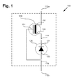
- Figure 1 illustrates a circuit diagram of a III-nitride transistor coupled with a Group IV diode, such as a silicon diode.
- a Group IV diode such as a silicon diode.
- references to a "silicon diode” are made for brevity and convenience only.
- the "Group IV or silicon diode” in the context of the present invention's stacked-die package can be replaced with a non-silicon diode or in general with any diode.
- Figure 1 includes terminals 112a and 112b, nodes 114 and 116, diode 120, and III-nitride transistor 130.
- III-nitride transistor 130 may, for example, comprise a gallium nitride (GaN) field effect transistor (FET), or a GaN high electron mobility transistor (HEMT), and may more specifically comprise a depletion-mode GaN transistor.
- Diode 120 can be either a PN junction diode or a Schottky diode.
- the cathode 121 of diode 120 is coupled to the source 133 of III-nitride transistor 130 at node 114. Additionally, a complete cascoded switch is formed by coupling the gate 131 of III-nitride transistor 130 to the anode 122 of diode 120 at node 116.
- the circuit of Figure 1 implements a high performance cascoded rectifier.
- the circuit may comprise a different configuration of diode 120 with III-nitride transistor 130.
- III-Nitride FET or III-Nitride HEMT it may be preferable to form the III-Nitride FET or III-Nitride HEMT as discussed in U.S. patent number 7,745,849 issued on 06/29/2010 titled “Enhancement Mode III-Nitride Semiconductor Device with Reduced Electric Field Between the Gate and the Drain,” U.S. patent number 7,759,699 issued on 07/20/2010 titled “III-Nitride Enhancement Mode Devices," U.S. patent number 7,382,001 issued on 06/03/2008 titled “Enhancement Mode III-Nitride FET,” U.S. patent number 7,112,830 issued on 09/26/2006 titled “Super Lattice Modification of Overlying Transistor,” U.S.
- III-Nitride FET be a high voltage III-N FET.
- III-N FET 130 may be optimized to operate with a V drain of between 200V - 5000V, or it may be preferred that FET 130 be optimized to operate between 500V - 700V or any other sub range between 200V - 5000V.
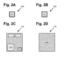
- Figure 2A illustrates a front side of a group IV diode
- Figure 2B illustrates a backside of a group IV diode
- Figure 2C illustrates a front side of a III-nitride transistor
- Figure 2D illustrates a backside of a III-nitride transistor.
- diode 220 may correspond to diode 120 from Figure 1
- III-nitride transistor 230 may correspond to III-nitride transistor 130 from Figure 1 .
- a die size of approximately 1mm x 1mm may be preferred for diode 220. In certain other embodiments, the die size of diode 220 may be larger or smaller.
- the silicon diode 220 includes an anode 222 on a top surface and a cathode 212 on an opposite bottom surface.
- the III-nitride transistor 230 includes a gate 231, a drain 232, and a source 233 on a top surface, whereas a bottom or backside surface is inactive.
- a die size of approximately 3.2mm x 2.795mm may be preferred for III-nitride transistor 230.
- the die size of III-nitride transistor 230 may be larger or smaller.
- Figures 2E, 2G , and 2I illustrate top views of a high voltage cascoded III-nitride rectifier package assembly, according to an embodiment of the invention.
- Figures 2F, 2H , 2J, 2K, and 2L also illustrate corresponding cross sectional views of a high voltage cascoded III-nitride rectifier package assembly, according to an embodiment of the invention.
- Figure 3 also illustrates a cross sectional view of a completed high voltage cascoded III-nitride rectifier package mounted to a system printed circuit board (PCB), according to an embodiment of the invention.
- PCB system printed circuit board
- package support surface 260 may comprise, for example, a single, dual, or multi layer printed circuit board (PCB). However, alternative embodiments may utilize other support surfaces, such as a ceramic substrate. Package support surface 260 may be approximately 125 microns thick, but any thickness may be selected to provide appropriate stiffness for conductive clips to be connected during assembly. In certain embodiments, package support surface 260 may also include thermal traces for improved heat dissipation.
- PCB printed circuit board
- FIG. 2E the backside 240 of III-nitride transistor 230 is coupled to package support surface 260 such that gate 231, drain 232, and source 233 are accessible on a top surface.
- Figure 2F also illustrates a cross sectional view corresponding to line 2F-2F in Figure 2E .
- package support surface 260 may accommodate multiple packages, for example in a strip or grid, which are later singulated into individual packages. Thus, multiple packages may be processed at the same time.
- diode 220 is stacked atop III-nitride transistor 230 such that the cathode 221 (not visible) resides on source 233.
- the anode 222 is accessible on a top surface of diode 220.
- solder such as a solder paste or a solder pre-form, may be applied to gate 231, drain 232, and source 233.
- other materials such as conductive adhesive or conductive tape may substitute for solder.
- Figure 2H also illustrates a cross sectional view corresponding to line 2H-2H in Figure 2G .
- conductive clips 212a and 212b may be picked and placed on top of package 210, as shown.
- a first conductive clip 212b is connected to anode 222 of diode 220 and gate 231 of III-nitride transistor 230
- a second conductive clip 212a is connected to drain 232 of III-nitride transistor 230.
- Conductive clips 212a and 212b may comprise, for example, copper or copper alloys.
- additional solder may be deposited on top of anode 222 of diode 220 and on top of package support surface 260.
- conductive clips 212a and 212b are further connected to package support surface 260 for mechanical support. Further, conductive clips 212a and 212b each have a respective flat portion 214a and 214b, suitable for surface mounting. The flat portions 214a and 214b may also be substantially coplanar to further facilitate surface mounting of package 210.
- conductive clips 212a and 212b connect to mating surfaces using straight connections, as shown in Figures 2J and 2K .
- conductive clip 212b is connected to anode 222 of diode 220 by a straight connection, as shown in Figure 2J .
- alternative embodiments may use various other connections including a screw-head, a nail-head, a mushroom connector, or a coin connector, depending on application requirements for mating surface area, mechanical stability, and ease of manufacture.
- the entire assembly may be heated, for example in a reflow or conveyor oven, to reflow the previously deposited solder.
- cathode 221 of diode 220 may be electrically and mechanically coupled to source 233 of III-nitride transistor 230
- conductive clip 212b may be connected to gate 231 of III-nitride transistor 230 and anode 222 of diode 220
- conductive clip 212a may be connected to drain 232 of III-nitride transistor 230.
- conductive clips 212a and 212b may each be connected to package support surface 260, which provides mechanical support and thermal dissipation for package 210.
- the cascoded rectifier circuit illustrated in diagram 100 of Figure 1 is provided, with conductive clip 212a corresponding to terminal 112a of Figure 1 and conductive clip 212b corresponding to terminal 112b of Figure 1 .
- an encapsulant such as glob-top 265 may optionally be applied to package 210, providing insulation and protection for III-nitride transistor 230 and diode 220.
- other encapsulants may be preferred, and the encapsulant may extend beyond the top edges of the stacked die assembly of III-nitride transistor 230 and diode 220.
- package 210 may be singulated and flipped onto system printed circuit board (PCB) 310, using conventional methods as known in the art.
- a distance of at least 2.7500 mm, for example 3.0000 mm, may be provided between flat portions 214a and 214b mounted on system PCB 310, enabling high voltage operation at 600V. It should be noted that only a portion of system PCB 310 is shown for simplicity, as package 210 may be integrated as part of a larger circuit on system PCB 310.
- a high voltage cascoded III-nitride rectifier package utilizing clips on a package support surface and methods for fabricating such a package have been described.
- the disclosed package provides a high voltage III-nitride cascoded rectifier in a compact package without using wire bonds.
- reduced package footprint, improved surge current capability, and higher performance may be achieved compared to conventional wire bonded packages.
- the package may utilize low cost package support surfaces such as single layer PCBs, expensive leadless package fabrication processes may be advantageously avoided, and available surface mount technology (SMT) manufacturing facilities may be utilized.
- SMT surface mount technology
Abstract
Description
- The present application claims the benefit of and priority to a pending provisional application entitled "High Voltage Cascoded GaN Rectifier Leadless Packages," Serial Number
61/482,314 filed on May 4, 2011 - The present invention relates generally to semiconductor devices. More particularly, the present invention relates to packaging of semiconductor devices.
- For high power and high performance circuit applications, III-nitride transistors such as gallium nitride (GaN) field effect transistors (FETs) are often desirable for their high efficiency and high voltage operation. In particular, it is often desirable to combine such III-nitride transistors with other devices, such as silicon diodes, to create high performance rectifiers such as cascoded rectifiers.
- Unfortunately, conventional package integration techniques for combining III-nitride transistors with silicon diodes often negate the benefits provided by such III-nitride transistors. For example, conventional package designs may require wire bonds to leads for terminal connections, undesirably increasing package form factor, manufacturing costs, parasitic inductance, resistance, and thermal dissipation requirements of the package. While quad flat no leads (QFN) packages are known to avoid wire bonds, such packages may undesirably require high cost fabrication facilities.
- Thus, a unique cost-effective solution is needed to support the cost effective fabrication of packages integrating high voltage cascoded III-nitride rectifiers.
- A high voltage cascoded III-nitride rectifier package utilizing clips on a package support surface, substantially as shown in and/or described in connection with at least one of the figures, and as set forth more completely in the claims.
-
-
Figure 1 illustrates a circuit diagram of a III-nitride transistor coupled with a Group IV diode. -
Figure 2A illustrates a front side of a group IV diode. -
Figure 2B illustrates a backside of a group IV diode. -
Figure 2C illustrates a front side of a III-nitride transistor. -
Figure 2D illustrates a backside of a III-nitride transistor. -
Figure 2E illustrates a top view of a high voltage cascoded III-nitride rectifier package assembly, according to an embodiment of the invention. -
Figure 2F illustrates a cross sectional view of a high voltage cascoded III-nitride rectifier package assembly, according to an embodiment of the invention. -
Figure 2G illustrates a top view of a high voltage cascoded III-nitride rectifier package assembly, according to an embodiment of the invention. -
Figure 2H illustrates a cross sectional view of a high voltage cascoded III-nitride rectifier package assembly, according to an embodiment of the invention. -
Figure 2I illustrates a top view of a high voltage cascoded III-nitride rectifier package assembly, according to an embodiment of the invention. -
Figure 2J illustrates a cross sectional view of a high voltage cascoded III-nitride rectifier package assembly, according to an embodiment of the invention. -
Figure 2K illustrates a cross sectional view of a high voltage cascoded III-nitride rectifier package assembly, according to an embodiment of the invention. -
Figure 2L illustrates a cross sectional view of a high voltage cascoded III-nitride rectifier package assembly, according to an embodiment of the invention. -
Figure 3 illustrates a cross sectional view of a high voltage cascoded III-nitride rectifier package mounted to a system printed circuit board (PCB), according to an embodiment of the invention. - The present application is directed to a high voltage cascoded III-nitride rectifier package utilizing clips on a package support surface. The following description contains specific information pertaining to the implementation of the present invention. One skilled in the art will recognize that the present invention may be implemented in a manner different from that specifically discussed in the present application. Moreover, some of the specific details of the invention are not discussed in order not to obscure the invention. The specific details not described in the present application are within the knowledge of a person of ordinary skill in the art.
- The drawings in the present application and their accompanying detailed description are directed to merely exemplary embodiments of the invention. To maintain brevity, other embodiments of the invention, which use the principles of the present invention, are not specifically described in the present application and are not specifically illustrated by the present drawings.
- As used herein, the phrase "III-Nitride or III-N" refers to a compound semiconductor that includes nitrogen and at least one group three element including Al, Ga, In and B, and including but not limited to any of its alloys, such as aluminum gallium nitride (AlxGa(1-x)N), indium gallium nitride (InyGa(1-y)N), aluminum indium gallium nitride (AlxInyGa(1-x-y)N), gallium arsenide phosphide nitride (GaAsaPb N(1-a-b)), aluminum indium gallium arsenide phosphide nitride (AlxInyGa(1-x-y)AsaPb N(1-a-b)), amongst others. III-nitride material also refers generally to any polarity including but not limited to Ga-polar, N-polar, semi-polar or non-polar crystal orientations. The III-Nitride material also includes either the Wurtzitic, Zincblende or mixed polytypes, and includes single-crystal, monocrystal, polycrystal or amorphous crystal structures.
- Also as used herein, the phrase "Group IV" refers to a semiconductor that includes at least one group four element including Si, Ge and C, and also includes compound semiconductors SiGe and SiC amongst others. Group IV also refers to semiconductor material which consists of layers of Group IV elements or doping of group IV elements to produce strained silicon or strained Group IV material, and also includes Group IV based composite substrates including SOI, SIMOX and SOS (silicon on sapphire), amongst others.
- U.S. patent application titled "III-Nitride Transistor Stacked with Diode in a Package," Serial No.
13/053,646 filed on 3/22/2011 - The present application addresses and discloses modifications needed to form a wire-bondless surface mountable high voltage semiconductor package for use in high voltage (200V-1200V or higher) applications. Additionally, the present application addresses and discloses the construction of such a package by describing the use of surface mountable conductive clips attached to a package support surface.
- The present application describes the physical arrangement of a stacked-die wire-bondless surface mountable high voltage package. In particular, a Group IV diode is stacked atop a III-N material transistor in a quad flat no-lead (QFN) package. Modifications required to accommodate the high voltage field differential between the anode and cathode of the device (>200V) include widening the physical separation between the anode and cathode to, for example, 2.7500 mm or greater.
-
Figure 1 illustrates a circuit diagram of a III-nitride transistor coupled with a Group IV diode, such as a silicon diode. In the present application, references to a "silicon diode" are made for brevity and convenience only. However, the "Group IV or silicon diode" in the context of the present invention's stacked-die package can be replaced with a non-silicon diode or in general with any diode.Figure 1 includesterminals nodes diode 120, and III-nitride transistor 130. III-nitride transistor 130 may, for example, comprise a gallium nitride (GaN) field effect transistor (FET), or a GaN high electron mobility transistor (HEMT), and may more specifically comprise a depletion-mode GaN transistor.Diode 120 can be either a PN junction diode or a Schottky diode. - In the example shown in
Figure 1 , thecathode 121 ofdiode 120 is coupled to thesource 133 of III-nitride transistor 130 atnode 114. Additionally, a complete cascoded switch is formed by coupling thegate 131 of III-nitride transistor 130 to theanode 122 ofdiode 120 atnode 116. Thus, the circuit ofFigure 1 implements a high performance cascoded rectifier. However, in alternative embodiments, the circuit may comprise a different configuration ofdiode 120 with III-nitride transistor 130. - It may be preferable to form the III-Nitride FET or III-Nitride HEMT as discussed in
U.S. patent number 7,745,849 issued on 06/29/2010 titled "Enhancement Mode III-Nitride Semiconductor Device with Reduced Electric Field Between the Gate and the Drain,"U.S. patent number 7,759,699 issued on 07/20/2010 titled "III-Nitride Enhancement Mode Devices,"U.S. patent number 7,382,001 issued on 06/03/2008 titled "Enhancement Mode III-Nitride FET,"U.S. patent number 7,112,830 issued on 09/26/2006 titled "Super Lattice Modification of Overlying Transistor,"U.S. patent number 7,456,442 issued on 11/25/2008 titled "Super Lattice Modification of Overlying Transistor,"U.S. patent number 7,339,205 issued on 03/04/2008 titled "Gallium Nitride Materials and Methods Associated with the Same,"U.S. patent number 6,849,882 issued on 02/01/2005 titled "Group-III Nitride Based High Electron Mobility Transistor (HEMT) with Barrier/Spacer Layer,"U.S. patent number 6,617,060 issued on 09/09/2003 titled "Gallium Nitride Materials and Methods,"U.S. patent number 6,649,287 issued on 11/18/2003 titled "Gallium Nitride Materials and Methods,"U.S. patent number 5,192,987 issued on 03/09/1993 titled "High Electron Mobility Transistor with GAN/ALXGA1-XN Heterojunctions," and U.S. patent application titled "Group III-V Semiconductor Device with Strain-Relieving Interlayers," Serial No.12/587,964 filed on 10/14/2009 12/928,946 filed on 12/21/2010 11/531,508 filed on 09/13/2006 13/021,437 filed on 2/4/2011 13/017,970 filed on 1/31/2011 12/653,097 filed on 12/7/2009 12/195,801 filed on 08/21/2008 12/211,120 filed on 09/16/2008 11/857,113 filed on 09/8/2007 61/447,479 filed on 2/28/2011 61/449,046 filed on 3/3/2011 N FET 130 may be optimized to operate with a Vdrain of between 200V - 5000V, or it may be preferred that FET 130 be optimized to operate between 500V - 700V or any other sub range between 200V - 5000V. - Turning to
Figures 2A-2D, Figure 2A illustrates a front side of a group IV diode,Figure 2B illustrates a backside of a group IV diode,Figure 2C illustrates a front side of a III-nitride transistor, andFigure 2D illustrates a backside of a III-nitride transistor. With respect toFigures 2A-2D ,diode 220 may correspond todiode 120 fromFigure 1 , and III-nitride transistor 230 may correspond to III-nitride transistor 130 fromFigure 1 . In certain embodiments, a die size of approximately 1mm x 1mm may be preferred fordiode 220. In certain other embodiments, the die size ofdiode 220 may be larger or smaller. As shown inFigures 2A and 2B , thesilicon diode 220 includes ananode 222 on a top surface and a cathode 212 on an opposite bottom surface. As shown inFigures 2C and 2D , the III-nitride transistor 230 includes agate 231, adrain 232, and asource 233 on a top surface, whereas a bottom or backside surface is inactive. In certain embodiments, a die size of approximately 3.2mm x 2.795mm may be preferred for III-nitride transistor 230. In certain other embodiments, the die size of III-nitride transistor 230 may be larger or smaller. - Next,
Figures 2E, 2G , and2I illustrate top views of a high voltage cascoded III-nitride rectifier package assembly, according to an embodiment of the invention.Figures 2F, 2H ,2J, 2K, and 2L also illustrate corresponding cross sectional views of a high voltage cascoded III-nitride rectifier package assembly, according to an embodiment of the invention.Figure 3 also illustrates a cross sectional view of a completed high voltage cascoded III-nitride rectifier package mounted to a system printed circuit board (PCB), according to an embodiment of the invention. - Starting with
Figure 2E , the III-nitride transistor 230 ofFigures 2C-2D is attached to packagesupport surface 260, for example by a die attach material.Package support surface 260 may comprise, for example, a single, dual, or multi layer printed circuit board (PCB). However, alternative embodiments may utilize other support surfaces, such as a ceramic substrate.Package support surface 260 may be approximately 125 microns thick, but any thickness may be selected to provide appropriate stiffness for conductive clips to be connected during assembly. In certain embodiments,package support surface 260 may also include thermal traces for improved heat dissipation. As shown inFigure 2E , thebackside 240 of III-nitride transistor 230 is coupled to packagesupport surface 260 such thatgate 231, drain 232, andsource 233 are accessible on a top surface.Figure 2F also illustrates a cross sectional view corresponding toline 2F-2F inFigure 2E . - For simplicity, the Figures may only illustrate the assembly of a single package. However, it is understood that
package support surface 260 may accommodate multiple packages, for example in a strip or grid, which are later singulated into individual packages. Thus, multiple packages may be processed at the same time. - From
Figure 2E to Figure 2G ,diode 220 is stacked atop III-nitride transistor 230 such that the cathode 221 (not visible) resides onsource 233. As a result, theanode 222 is accessible on a top surface ofdiode 220. Prior to such stacking, solder, such as a solder paste or a solder pre-form, may be applied togate 231, drain 232, andsource 233. Alternatively, other materials such as conductive adhesive or conductive tape may substitute for solder.Figure 2H also illustrates a cross sectional view corresponding toline 2H-2H inFigure 2G . - From
Figure 2G to Figure 2I ,conductive clips package 210, as shown. Thus, a firstconductive clip 212b is connected to anode 222 ofdiode 220 andgate 231 of III-nitride transistor 230, and a secondconductive clip 212a is connected to drain 232 of III-nitride transistor 230.Conductive clips anode 222 ofdiode 220 and on top ofpackage support surface 260. As shown inFigures 2J and 2K ,conductive clips support surface 260 for mechanical support. Further,conductive clips flat portion flat portions package 210. - The ends of
conductive clips Figures 2J and 2K . For example,conductive clip 212b is connected to anode 222 ofdiode 220 by a straight connection, as shown inFigure 2J . However, alternative embodiments may use various other connections including a screw-head, a nail-head, a mushroom connector, or a coin connector, depending on application requirements for mating surface area, mechanical stability, and ease of manufacture. - After picking and placing
conductive clips cathode 221 ofdiode 220 may be electrically and mechanically coupled tosource 233 of III-nitride transistor 230,conductive clip 212b may be connected togate 231 of III-nitride transistor 230 andanode 222 ofdiode 220, andconductive clip 212a may be connected to drain 232 of III-nitride transistor 230. Further,conductive clips support surface 260, which provides mechanical support and thermal dissipation forpackage 210. Thus, the cascoded rectifier circuit illustrated in diagram 100 ofFigure 1 is provided, withconductive clip 212a corresponding to terminal 112a ofFigure 1 andconductive clip 212b corresponding to terminal 112b ofFigure 1 . - From
Figure 2K to Figure 2L , an encapsulant such as glob-top 265 may optionally be applied topackage 210, providing insulation and protection for III-nitride transistor 230 anddiode 220. In certain other embodiments, other encapsulants may be preferred, and the encapsulant may extend beyond the top edges of the stacked die assembly of III-nitride transistor 230 anddiode 220. - From
Figure 2L to Figure 3 ,package 210 may be singulated and flipped onto system printed circuit board (PCB) 310, using conventional methods as known in the art. A distance of at least 2.7500 mm, for example 3.0000 mm, may be provided betweenflat portions system PCB 310, enabling high voltage operation at 600V. It should be noted that only a portion ofsystem PCB 310 is shown for simplicity, aspackage 210 may be integrated as part of a larger circuit onsystem PCB 310. - Thus, a high voltage cascoded III-nitride rectifier package utilizing clips on a package support surface and methods for fabricating such a package have been described. The disclosed package provides a high voltage III-nitride cascoded rectifier in a compact package without using wire bonds. As a result, reduced package footprint, improved surge current capability, and higher performance may be achieved compared to conventional wire bonded packages. Since the package may utilize low cost package support surfaces such as single layer PCBs, expensive leadless package fabrication processes may be advantageously avoided, and available surface mount technology (SMT) manufacturing facilities may be utilized. Furthermore, since multiple packages may be assembled at a time, high integration and cost savings may be achieved compared to conventional methods requiring individual package processing.
- From the above description of the invention it is manifest that various techniques can be used for implementing the concepts of the present invention without departing from its scope. Moreover, while the invention has been described with specific reference to certain embodiments, a person of ordinary skills in the art would recognize that changes can be made in form and detail without departing from the spirit and the scope of the invention. As such, the described embodiments are to be considered in all respects as illustrative and not restrictive. It should also be understood that the invention is not limited to the particular embodiments described herein, but is capable of many rearrangements, modifications, and substitutions without departing from the scope of the invention.
Claims (15)
- A wire-bondless surface mountable high voltage semiconductor package comprising:a package support surface;a III-nitride transistor having a gate, a source, and a drain, said III-nitride transistor attached to said package support surface;a diode having an anode and a cathode, said diode stacked over said III-nitride transistor such that said cathode is mechanically and electrically coupled to said source;a first conductive clip connected to said gate of said III-nitride transistor, said anode of said diode, and said package support surface;a second conductive clip connected to said drain of said III-nitride transistor, and said package support surface;said first conductive clip and second conductive clip each having respective flat portions for surface mounting said high voltage semiconductor package.
- The high voltage semiconductor package of claim 1, wherein said respective flat portions are substantially coplanar.
- The high voltage semiconductor package of claim 1, further comprising a glob-top encapsulating said III-nitride transistor and said diode.
- The high voltage semiconductor package of claim 3, wherein said glob-top extends beyond top edges of said III-nitride transistor.
- The high voltage semiconductor package of claim 1, wherein said first conductive clip is connected to said anode by a connector selected from the group consisting of a coin connector, a mushroom connector, a nail-head, a screw-head, and a straight connector.
- The high voltage semiconductor package of claim 1, wherein said first and second conductive clips comprise copper.
- The high voltage semiconductor package of claim 1, wherein said package support surface comprises a printed circuit board (PCB).
- The high voltage semiconductor package of claim 1, wherein said package support surface includes thermal traces.
- The high voltage semiconductor package of claim 1, wherein said diode is a Schottky diode.
- The high voltage semiconductor package of claim 1, wherein said III-nitride transistor is a GaN FET.
- The high voltage semiconductor package of claim 1, wherein said III-nitride transistor is a GaN HEMT.
- A method for manufacturing a wire-bondless surface mountable high voltage semiconductor package, said method comprising:attaching, to a package support surface, a III-nitride transistor having a gate, a source, and a drain;stacking over said source of said III-nitride transistor a diode having a cathode and an anode;connecting a first conductive clip to said gate of said III-nitride transistor, said anode of said diode, and said package support surface;connecting a second conductive clip to said drain of said III-nitride transistor and said package support surface;said first conductive clip and second conductive clip each having respective flat portions for surface mounting said high voltage semiconductor package.
- The method of claim 12, wherein said respective flat portions are substantially coplanar.
- The method of claim 12, further comprising encapsulating said III-nitride transistor and said diode with a glob-top.
- The method of claim 12, wherein said first and second conductive clips comprise copper.
Applications Claiming Priority (2)
| Application Number | Priority Date | Filing Date | Title |
|---|---|---|---|
| US201161482314P | 2011-05-04 | 2011-05-04 | |
| US13/364,242 US8546849B2 (en) | 2011-05-04 | 2012-02-01 | High voltage cascoded III-nitride rectifier package utilizing clips on package surface |
Publications (2)
| Publication Number | Publication Date |
|---|---|
| EP2521176A1 true EP2521176A1 (en) | 2012-11-07 |
| EP2521176B1 EP2521176B1 (en) | 2014-06-11 |
Family
ID=45992088
Family Applications (1)
| Application Number | Title | Priority Date | Filing Date |
|---|---|---|---|
| EP20120163619 Active EP2521176B1 (en) | 2011-05-04 | 2012-04-10 | High voltage cascoded III-nitride rectifier package comprising conductive clips between electrodes of components and the surface of a package support member |
Country Status (3)
| Country | Link |
|---|---|
| US (3) | US8546849B2 (en) |
| EP (1) | EP2521176B1 (en) |
| JP (1) | JP5650686B2 (en) |
Families Citing this family (16)
| Publication number | Priority date | Publication date | Assignee | Title |
|---|---|---|---|---|
| US8570012B2 (en) * | 2011-12-13 | 2013-10-29 | Texas Instruments Incorporated | Diode for use in a switched mode power supply |
| KR101919421B1 (en) * | 2012-08-16 | 2018-11-19 | 삼성전자주식회사 | Semiconductor device and method of manufacturing the same |
| US9202811B2 (en) * | 2012-12-18 | 2015-12-01 | Infineon Technologies Americas Corp. | Cascode circuit integration of group III-N and group IV devices |
| EP2787641B1 (en) * | 2013-04-05 | 2018-08-29 | Nexperia B.V. | Cascoded semiconductor devices |
| KR102066620B1 (en) * | 2013-07-18 | 2020-01-16 | 엘지이노텍 주식회사 | A light emitting device |
| US9362240B2 (en) | 2013-12-06 | 2016-06-07 | Infineon Technologies Austria Ag | Electronic device |
| MY171261A (en) * | 2014-02-19 | 2019-10-07 | Carsem M Sdn Bhd | Stacked electronic packages |
| JP6924555B2 (en) * | 2015-03-02 | 2021-08-25 | 晶元光電股▲ふん▼有限公司Epistar Corporation | LED drive and related lighting system |
| TWI678944B (en) * | 2015-10-23 | 2019-12-01 | 晶元光電股份有限公司 | Led driver and illumination system related to the same |
| USRE48798E1 (en) * | 2015-03-02 | 2021-10-26 | Epistar Corporation | LED driver and illumination system related to the same |
| TWI663893B (en) * | 2015-03-02 | 2019-06-21 | 晶元光電股份有限公司 | Led driver and illumination system related to the same |
| TWI678946B (en) * | 2015-03-26 | 2019-12-01 | 晶元光電股份有限公司 | Led driver and illumination system related to the same |
| TWI729540B (en) * | 2015-03-26 | 2021-06-01 | 晶元光電股份有限公司 | Led driver and illumination system related to the same |
| TWI726085B (en) | 2017-04-05 | 2021-05-01 | 晶元光電股份有限公司 | Led driver |
| US10848074B2 (en) | 2018-10-12 | 2020-11-24 | Electronics And Telecommunications Research Institute | High voltage bridge rectifier |
| FR3097682B1 (en) * | 2019-06-19 | 2023-01-13 | St Microelectronics Gmbh | Monolithic component comprising a gallium nitride power transistor |
Citations (14)
| Publication number | Priority date | Publication date | Assignee | Title |
|---|---|---|---|---|
| US5192987A (en) | 1991-05-17 | 1993-03-09 | Apa Optics, Inc. | High electron mobility transistor with GaN/Alx Ga1-x N heterojunctions |
| JP2003197859A (en) * | 2001-12-26 | 2003-07-11 | Toyota Motor Corp | Junction structure of semiconductor module |
| US6617060B2 (en) | 2000-12-14 | 2003-09-09 | Nitronex Corporation | Gallium nitride materials and methods |
| US6849882B2 (en) | 2001-05-11 | 2005-02-01 | Cree Inc. | Group-III nitride based high electron mobility transistor (HEMT) with barrier/spacer layer |
| US20050285249A1 (en) * | 2004-06-28 | 2005-12-29 | Semiconductor Components Industries, Llc | Multi-chip semiconductor connector assemblies |
| US7112830B2 (en) | 2002-11-25 | 2006-09-26 | Apa Enterprises, Inc. | Super lattice modification of overlying transistor |
| US20070063216A1 (en) * | 2005-09-21 | 2007-03-22 | International Rectifier Corporation | Semiconductor package |
| US20070176291A1 (en) * | 2005-12-30 | 2007-08-02 | Chuan Cheah | Cascoded rectifier package |
| US7339205B2 (en) | 2004-06-28 | 2008-03-04 | Nitronex Corporation | Gallium nitride materials and methods associated with the same |
| US7382001B2 (en) | 2004-01-23 | 2008-06-03 | International Rectifier Corporation | Enhancement mode III-nitride FET |
| US20080191216A1 (en) * | 2007-02-09 | 2008-08-14 | Sanken Electric Co., Ltd. | Diode-Like Composite Semiconductor Device |
| US20090189291A1 (en) * | 2008-01-24 | 2009-07-30 | Infineon Technologies Ag | Multi-chip module |
| US7745849B2 (en) | 2007-09-20 | 2010-06-29 | International Rectifier Corporation | Enhancement mode III-nitride semiconductor device with reduced electric field between the gate and the drain |
| US7759699B2 (en) | 2005-07-06 | 2010-07-20 | International Rectifier Corporation | III-nitride enhancement mode devices |
Family Cites Families (26)
| Publication number | Priority date | Publication date | Assignee | Title |
|---|---|---|---|---|
| US7017A (en) * | 1850-01-15 | Brick-pbess | ||
| US9018A (en) * | 1852-06-15 | Machine for polishing daguerreotype-plates | ||
| JPH062687A (en) | 1992-06-19 | 1994-01-11 | Matsushita Refrig Co Ltd | Oil cooler for horizontal type rotary compressor |
| JPH1197570A (en) | 1997-09-17 | 1999-04-09 | Hitachi Ltd | Semiconductor device manufacture thereof and packaging method therefor |
| JP2000223815A (en) | 1999-02-03 | 2000-08-11 | Matsushita Electric Ind Co Ltd | Mounting technique for resin molded substrate |
| JP3850739B2 (en) | 2002-02-21 | 2006-11-29 | 三菱電機株式会社 | Semiconductor device |
| WO2006068641A1 (en) | 2004-12-20 | 2006-06-29 | Semiconductor Components Industries, L.L.C. | Electronic package having down-set leads and method |
| JP2007027404A (en) | 2005-07-15 | 2007-02-01 | Sanyo Electric Co Ltd | Semiconductor device |
| US8482035B2 (en) | 2005-07-29 | 2013-07-09 | International Rectifier Corporation | Enhancement mode III-nitride transistors with single gate Dielectric structure |
| US8183595B2 (en) | 2005-07-29 | 2012-05-22 | International Rectifier Corporation | Normally off III-nitride semiconductor device having a programmable gate |
| US9157169B2 (en) | 2005-09-14 | 2015-10-13 | International Rectifier Corporation | Process for manufacture of super lattice using alternating high and low temperature layers to block parasitic current path |
| US7663212B2 (en) * | 2006-03-21 | 2010-02-16 | Infineon Technologies Ag | Electronic component having exposed surfaces |
| US7271470B1 (en) | 2006-05-31 | 2007-09-18 | Infineon Technologies Ag | Electronic component having at least two semiconductor power devices |
| US8791503B2 (en) | 2007-09-18 | 2014-07-29 | International Rectifier Corporation | III-nitride semiconductor device with reduced electric field between gate and drain and process for its manufacture |
| US8350296B2 (en) | 2008-08-21 | 2013-01-08 | International Rectifier Corporation | Enhancement mode III-nitride device with floating gate and process for its manufacture |
| US8178954B2 (en) | 2009-07-31 | 2012-05-15 | Alpha & Omega Semiconductor, Inc. | Structure of mixed semiconductor encapsulation structure with multiple chips and capacitors |
| US8575660B2 (en) | 2009-10-14 | 2013-11-05 | International Rectifier Corporation | Group III-V semiconductor device with strain-relieving interlayers |
| US20110133337A1 (en) | 2009-10-19 | 2011-06-09 | Jeng-Jye Shau | Area reduction for surface mount package chips |
| US7939370B1 (en) | 2009-10-29 | 2011-05-10 | Alpha And Omega Semiconductor Incorporated | Power semiconductor package |
| US8269259B2 (en) | 2009-12-07 | 2012-09-18 | International Rectifier Corporation | Gated AlGaN/GaN heterojunction Schottky device |
| US9105703B2 (en) | 2010-03-22 | 2015-08-11 | International Rectifier Corporation | Programmable III-nitride transistor with aluminum-doped gate |
| US20120153351A1 (en) | 2010-12-21 | 2012-06-21 | International Rectifier Corporation | Stress modulated group III-V semiconductor device and related method |
| US8963338B2 (en) * | 2011-03-02 | 2015-02-24 | International Rectifier Corporation | III-nitride transistor stacked with diode in a package |
| US20120228696A1 (en) | 2011-03-07 | 2012-09-13 | Texas Instruments Incorporated | Stacked die power converter |
| US8853707B2 (en) * | 2011-05-04 | 2014-10-07 | International Rectifier Corporation | High voltage cascoded III-nitride rectifier package with etched leadframe |
| US8853706B2 (en) * | 2011-05-04 | 2014-10-07 | International Rectifier Corporation | High voltage cascoded III-nitride rectifier package with stamped leadframe |
-
2012
- 2012-02-01 US US13/364,242 patent/US8546849B2/en active Active
- 2012-04-10 EP EP20120163619 patent/EP2521176B1/en active Active
- 2012-04-17 JP JP2012094150A patent/JP5650686B2/en active Active
-
2013
- 2013-09-26 US US14/038,384 patent/US8790965B2/en active Active
-
2014
- 2014-07-16 US US14/333,401 patent/US9142503B2/en active Active
Patent Citations (16)
| Publication number | Priority date | Publication date | Assignee | Title |
|---|---|---|---|---|
| US5192987A (en) | 1991-05-17 | 1993-03-09 | Apa Optics, Inc. | High electron mobility transistor with GaN/Alx Ga1-x N heterojunctions |
| US6617060B2 (en) | 2000-12-14 | 2003-09-09 | Nitronex Corporation | Gallium nitride materials and methods |
| US6649287B2 (en) | 2000-12-14 | 2003-11-18 | Nitronex Corporation | Gallium nitride materials and methods |
| US6849882B2 (en) | 2001-05-11 | 2005-02-01 | Cree Inc. | Group-III nitride based high electron mobility transistor (HEMT) with barrier/spacer layer |
| JP2003197859A (en) * | 2001-12-26 | 2003-07-11 | Toyota Motor Corp | Junction structure of semiconductor module |
| US7456442B2 (en) | 2002-11-25 | 2008-11-25 | International Rectifier Corporation | Super lattice modification of overlying transistor |
| US7112830B2 (en) | 2002-11-25 | 2006-09-26 | Apa Enterprises, Inc. | Super lattice modification of overlying transistor |
| US7382001B2 (en) | 2004-01-23 | 2008-06-03 | International Rectifier Corporation | Enhancement mode III-nitride FET |
| US7339205B2 (en) | 2004-06-28 | 2008-03-04 | Nitronex Corporation | Gallium nitride materials and methods associated with the same |
| US20050285249A1 (en) * | 2004-06-28 | 2005-12-29 | Semiconductor Components Industries, Llc | Multi-chip semiconductor connector assemblies |
| US7759699B2 (en) | 2005-07-06 | 2010-07-20 | International Rectifier Corporation | III-nitride enhancement mode devices |
| US20070063216A1 (en) * | 2005-09-21 | 2007-03-22 | International Rectifier Corporation | Semiconductor package |
| US20070176291A1 (en) * | 2005-12-30 | 2007-08-02 | Chuan Cheah | Cascoded rectifier package |
| US20080191216A1 (en) * | 2007-02-09 | 2008-08-14 | Sanken Electric Co., Ltd. | Diode-Like Composite Semiconductor Device |
| US7745849B2 (en) | 2007-09-20 | 2010-06-29 | International Rectifier Corporation | Enhancement mode III-nitride semiconductor device with reduced electric field between the gate and the drain |
| US20090189291A1 (en) * | 2008-01-24 | 2009-07-30 | Infineon Technologies Ag | Multi-chip module |
Also Published As
| Publication number | Publication date |
|---|---|
| JP2012235101A (en) | 2012-11-29 |
| US9142503B2 (en) | 2015-09-22 |
| JP5650686B2 (en) | 2015-01-07 |
| US20120280247A1 (en) | 2012-11-08 |
| US20140327014A1 (en) | 2014-11-06 |
| US8546849B2 (en) | 2013-10-01 |
| EP2521176B1 (en) | 2014-06-11 |
| US8790965B2 (en) | 2014-07-29 |
| US20140030854A1 (en) | 2014-01-30 |
Similar Documents
| Publication | Publication Date | Title |
|---|---|---|
| US9142503B2 (en) | III-nitride rectifier package | |
| EP2511953B1 (en) | Stacked composite device including a group III-V transistor and a group IV lateral transistor | |
| US9362267B2 (en) | Group III-V and group IV composite switch | |
| US9041067B2 (en) | Integrated half-bridge circuit with low side and high side composite switches | |
| JP5632416B2 (en) | Stacked composite device comprising a III-V transistor and a IV group vertical transistor | |
| EP2521171B1 (en) | High voltage cascoded III-nitride rectifier package with stamped leadframe | |
| EP3007227B1 (en) | Compact power semiconductor package | |
| JP5643783B2 (en) | Stacked composite device comprising a III-V transistor and a group IV diode | |
| EP2521172B1 (en) | Method of manufacturing a high voltage cascoded III-nitride rectifier package with etched leadframe | |
| US20130175542A1 (en) | Group III-V and Group IV Composite Diode | |
| US9202811B2 (en) | Cascode circuit integration of group III-N and group IV devices | |
| EP2639832A2 (en) | Group III-V and group IV composite diode |
Legal Events
| Date | Code | Title | Description |
|---|---|---|---|
| PUAI | Public reference made under article 153(3) epc to a published international application that has entered the european phase |
Free format text: ORIGINAL CODE: 0009012 |
|
| AK | Designated contracting states |
Kind code of ref document: A1 Designated state(s): AL AT BE BG CH CY CZ DE DK EE ES FI FR GB GR HR HU IE IS IT LI LT LU LV MC MK MT NL NO PL PT RO RS SE SI SK SM TR |
|
| AX | Request for extension of the european patent |
Extension state: BA ME |
|
| 17P | Request for examination filed |
Effective date: 20130507 |
|
| GRAP | Despatch of communication of intention to grant a patent |
Free format text: ORIGINAL CODE: EPIDOSNIGR1 |
|
| RIC1 | Information provided on ipc code assigned before grant |
Ipc: H01L 23/495 20060101ALI20131206BHEP Ipc: H03K 17/567 20060101ALI20131206BHEP Ipc: H03K 17/687 20060101ALI20131206BHEP Ipc: H01L 25/18 20060101AFI20131206BHEP Ipc: H03K 17/74 20060101ALI20131206BHEP |
|
| INTG | Intention to grant announced |
Effective date: 20140116 |
|
| GRAS | Grant fee paid |
Free format text: ORIGINAL CODE: EPIDOSNIGR3 |
|
| GRAA | (expected) grant |
Free format text: ORIGINAL CODE: 0009210 |
|
| AK | Designated contracting states |
Kind code of ref document: B1 Designated state(s): AL AT BE BG CH CY CZ DE DK EE ES FI FR GB GR HR HU IE IS IT LI LT LU LV MC MK MT NL NO PL PT RO RS SE SI SK SM TR |
|
| REG | Reference to a national code |
Ref country code: GB Ref legal event code: FG4D |
|
| REG | Reference to a national code |
Ref country code: CH Ref legal event code: EP |
|
| REG | Reference to a national code |
Ref country code: IE Ref legal event code: FG4D |
|
| REG | Reference to a national code |
Ref country code: AT Ref legal event code: REF Ref document number: 672611 Country of ref document: AT Kind code of ref document: T Effective date: 20140715 |
|
| REG | Reference to a national code |
Ref country code: DE Ref legal event code: R096 Ref document number: 602012002024 Country of ref document: DE Effective date: 20140731 |
|
| PG25 | Lapsed in a contracting state [announced via postgrant information from national office to epo] |
Ref country code: FI Free format text: LAPSE BECAUSE OF FAILURE TO SUBMIT A TRANSLATION OF THE DESCRIPTION OR TO PAY THE FEE WITHIN THE PRESCRIBED TIME-LIMIT Effective date: 20140611 Ref country code: LT Free format text: LAPSE BECAUSE OF FAILURE TO SUBMIT A TRANSLATION OF THE DESCRIPTION OR TO PAY THE FEE WITHIN THE PRESCRIBED TIME-LIMIT Effective date: 20140611 Ref country code: GR Free format text: LAPSE BECAUSE OF FAILURE TO SUBMIT A TRANSLATION OF THE DESCRIPTION OR TO PAY THE FEE WITHIN THE PRESCRIBED TIME-LIMIT Effective date: 20140912 Ref country code: NO Free format text: LAPSE BECAUSE OF FAILURE TO SUBMIT A TRANSLATION OF THE DESCRIPTION OR TO PAY THE FEE WITHIN THE PRESCRIBED TIME-LIMIT Effective date: 20140911 |
|
| REG | Reference to a national code |
Ref country code: NL Ref legal event code: VDEP Effective date: 20140611 |
|
| REG | Reference to a national code |
Ref country code: AT Ref legal event code: MK05 Ref document number: 672611 Country of ref document: AT Kind code of ref document: T Effective date: 20140611 |
|
| REG | Reference to a national code |
Ref country code: LT Ref legal event code: MG4D |
|
| PG25 | Lapsed in a contracting state [announced via postgrant information from national office to epo] |
Ref country code: SE Free format text: LAPSE BECAUSE OF FAILURE TO SUBMIT A TRANSLATION OF THE DESCRIPTION OR TO PAY THE FEE WITHIN THE PRESCRIBED TIME-LIMIT Effective date: 20140611 Ref country code: LV Free format text: LAPSE BECAUSE OF FAILURE TO SUBMIT A TRANSLATION OF THE DESCRIPTION OR TO PAY THE FEE WITHIN THE PRESCRIBED TIME-LIMIT Effective date: 20140611 Ref country code: HR Free format text: LAPSE BECAUSE OF FAILURE TO SUBMIT A TRANSLATION OF THE DESCRIPTION OR TO PAY THE FEE WITHIN THE PRESCRIBED TIME-LIMIT Effective date: 20140611 Ref country code: RS Free format text: LAPSE BECAUSE OF FAILURE TO SUBMIT A TRANSLATION OF THE DESCRIPTION OR TO PAY THE FEE WITHIN THE PRESCRIBED TIME-LIMIT Effective date: 20140611 |
|
| PG25 | Lapsed in a contracting state [announced via postgrant information from national office to epo] |
Ref country code: RO Free format text: LAPSE BECAUSE OF FAILURE TO SUBMIT A TRANSLATION OF THE DESCRIPTION OR TO PAY THE FEE WITHIN THE PRESCRIBED TIME-LIMIT Effective date: 20140611 Ref country code: SK Free format text: LAPSE BECAUSE OF FAILURE TO SUBMIT A TRANSLATION OF THE DESCRIPTION OR TO PAY THE FEE WITHIN THE PRESCRIBED TIME-LIMIT Effective date: 20140611 Ref country code: PT Free format text: LAPSE BECAUSE OF FAILURE TO SUBMIT A TRANSLATION OF THE DESCRIPTION OR TO PAY THE FEE WITHIN THE PRESCRIBED TIME-LIMIT Effective date: 20141013 Ref country code: ES Free format text: LAPSE BECAUSE OF FAILURE TO SUBMIT A TRANSLATION OF THE DESCRIPTION OR TO PAY THE FEE WITHIN THE PRESCRIBED TIME-LIMIT Effective date: 20140611 Ref country code: EE Free format text: LAPSE BECAUSE OF FAILURE TO SUBMIT A TRANSLATION OF THE DESCRIPTION OR TO PAY THE FEE WITHIN THE PRESCRIBED TIME-LIMIT Effective date: 20140611 Ref country code: CZ Free format text: LAPSE BECAUSE OF FAILURE TO SUBMIT A TRANSLATION OF THE DESCRIPTION OR TO PAY THE FEE WITHIN THE PRESCRIBED TIME-LIMIT Effective date: 20140611 |
|
| PG25 | Lapsed in a contracting state [announced via postgrant information from national office to epo] |
Ref country code: AT Free format text: LAPSE BECAUSE OF FAILURE TO SUBMIT A TRANSLATION OF THE DESCRIPTION OR TO PAY THE FEE WITHIN THE PRESCRIBED TIME-LIMIT Effective date: 20140611 Ref country code: PL Free format text: LAPSE BECAUSE OF FAILURE TO SUBMIT A TRANSLATION OF THE DESCRIPTION OR TO PAY THE FEE WITHIN THE PRESCRIBED TIME-LIMIT Effective date: 20140611 Ref country code: IS Free format text: LAPSE BECAUSE OF FAILURE TO SUBMIT A TRANSLATION OF THE DESCRIPTION OR TO PAY THE FEE WITHIN THE PRESCRIBED TIME-LIMIT Effective date: 20141011 Ref country code: NL Free format text: LAPSE BECAUSE OF FAILURE TO SUBMIT A TRANSLATION OF THE DESCRIPTION OR TO PAY THE FEE WITHIN THE PRESCRIBED TIME-LIMIT Effective date: 20140611 |
|
| REG | Reference to a national code |
Ref country code: DE Ref legal event code: R097 Ref document number: 602012002024 Country of ref document: DE |
|
| PLBE | No opposition filed within time limit |
Free format text: ORIGINAL CODE: 0009261 |
|
| STAA | Information on the status of an ep patent application or granted ep patent |
Free format text: STATUS: NO OPPOSITION FILED WITHIN TIME LIMIT |
|
| PG25 | Lapsed in a contracting state [announced via postgrant information from national office to epo] |
Ref country code: IT Free format text: LAPSE BECAUSE OF FAILURE TO SUBMIT A TRANSLATION OF THE DESCRIPTION OR TO PAY THE FEE WITHIN THE PRESCRIBED TIME-LIMIT Effective date: 20140611 Ref country code: DK Free format text: LAPSE BECAUSE OF FAILURE TO SUBMIT A TRANSLATION OF THE DESCRIPTION OR TO PAY THE FEE WITHIN THE PRESCRIBED TIME-LIMIT Effective date: 20140611 |
|
| 26N | No opposition filed |
Effective date: 20150312 |
|
| REG | Reference to a national code |
Ref country code: DE Ref legal event code: R097 Ref document number: 602012002024 Country of ref document: DE Effective date: 20150312 |
|
| PG25 | Lapsed in a contracting state [announced via postgrant information from national office to epo] |
Ref country code: BE Free format text: LAPSE BECAUSE OF FAILURE TO SUBMIT A TRANSLATION OF THE DESCRIPTION OR TO PAY THE FEE WITHIN THE PRESCRIBED TIME-LIMIT Effective date: 20140611 |
|
| PG25 | Lapsed in a contracting state [announced via postgrant information from national office to epo] |
Ref country code: SI Free format text: LAPSE BECAUSE OF FAILURE TO SUBMIT A TRANSLATION OF THE DESCRIPTION OR TO PAY THE FEE WITHIN THE PRESCRIBED TIME-LIMIT Effective date: 20140611 |
|
| PG25 | Lapsed in a contracting state [announced via postgrant information from national office to epo] |
Ref country code: LU Free format text: LAPSE BECAUSE OF FAILURE TO SUBMIT A TRANSLATION OF THE DESCRIPTION OR TO PAY THE FEE WITHIN THE PRESCRIBED TIME-LIMIT Effective date: 20150410 Ref country code: MC Free format text: LAPSE BECAUSE OF FAILURE TO SUBMIT A TRANSLATION OF THE DESCRIPTION OR TO PAY THE FEE WITHIN THE PRESCRIBED TIME-LIMIT Effective date: 20140611 |
|
| REG | Reference to a national code |
Ref country code: CH Ref legal event code: PL |
|
| REG | Reference to a national code |
Ref country code: IE Ref legal event code: MM4A |
|
| PG25 | Lapsed in a contracting state [announced via postgrant information from national office to epo] |
Ref country code: CH Free format text: LAPSE BECAUSE OF NON-PAYMENT OF DUE FEES Effective date: 20150430 Ref country code: LI Free format text: LAPSE BECAUSE OF NON-PAYMENT OF DUE FEES Effective date: 20150430 |
|
| REG | Reference to a national code |
Ref country code: FR Ref legal event code: ST Effective date: 20151231 |
|
| PG25 | Lapsed in a contracting state [announced via postgrant information from national office to epo] |
Ref country code: FR Free format text: LAPSE BECAUSE OF NON-PAYMENT OF DUE FEES Effective date: 20150430 |
|
| PG25 | Lapsed in a contracting state [announced via postgrant information from national office to epo] |
Ref country code: IE Free format text: LAPSE BECAUSE OF NON-PAYMENT OF DUE FEES Effective date: 20150410 |
|
| GBPC | Gb: european patent ceased through non-payment of renewal fee |
Effective date: 20160410 |
|
| PG25 | Lapsed in a contracting state [announced via postgrant information from national office to epo] |
Ref country code: MT Free format text: LAPSE BECAUSE OF FAILURE TO SUBMIT A TRANSLATION OF THE DESCRIPTION OR TO PAY THE FEE WITHIN THE PRESCRIBED TIME-LIMIT Effective date: 20140611 |
|
| PG25 | Lapsed in a contracting state [announced via postgrant information from national office to epo] |
Ref country code: GB Free format text: LAPSE BECAUSE OF NON-PAYMENT OF DUE FEES Effective date: 20160410 |
|
| PG25 | Lapsed in a contracting state [announced via postgrant information from national office to epo] |
Ref country code: BG Free format text: LAPSE BECAUSE OF FAILURE TO SUBMIT A TRANSLATION OF THE DESCRIPTION OR TO PAY THE FEE WITHIN THE PRESCRIBED TIME-LIMIT Effective date: 20140611 Ref country code: SM Free format text: LAPSE BECAUSE OF FAILURE TO SUBMIT A TRANSLATION OF THE DESCRIPTION OR TO PAY THE FEE WITHIN THE PRESCRIBED TIME-LIMIT Effective date: 20140611 Ref country code: HU Free format text: LAPSE BECAUSE OF FAILURE TO SUBMIT A TRANSLATION OF THE DESCRIPTION OR TO PAY THE FEE WITHIN THE PRESCRIBED TIME-LIMIT; INVALID AB INITIO Effective date: 20120410 |
|
| PG25 | Lapsed in a contracting state [announced via postgrant information from national office to epo] |
Ref country code: CY Free format text: LAPSE BECAUSE OF FAILURE TO SUBMIT A TRANSLATION OF THE DESCRIPTION OR TO PAY THE FEE WITHIN THE PRESCRIBED TIME-LIMIT Effective date: 20140611 |
|
| PG25 | Lapsed in a contracting state [announced via postgrant information from national office to epo] |
Ref country code: TR Free format text: LAPSE BECAUSE OF FAILURE TO SUBMIT A TRANSLATION OF THE DESCRIPTION OR TO PAY THE FEE WITHIN THE PRESCRIBED TIME-LIMIT Effective date: 20140611 |
|
| PG25 | Lapsed in a contracting state [announced via postgrant information from national office to epo] |
Ref country code: MK Free format text: LAPSE BECAUSE OF FAILURE TO SUBMIT A TRANSLATION OF THE DESCRIPTION OR TO PAY THE FEE WITHIN THE PRESCRIBED TIME-LIMIT Effective date: 20140611 |
|
| REG | Reference to a national code |
Ref country code: DE Ref legal event code: R082 Ref document number: 602012002024 Country of ref document: DE Representative=s name: DR. WEITZEL & PARTNER PATENT- UND RECHTSANWAEL, DE Ref country code: DE Ref legal event code: R081 Ref document number: 602012002024 Country of ref document: DE Owner name: INFINEON TECHNOLOGIES AMERICAS CORP., EL SEGUN, US Free format text: FORMER OWNER: INTERNATIONAL RECTIFIER CORP., EL SEGUNDO, CALIF., US |
|
| PG25 | Lapsed in a contracting state [announced via postgrant information from national office to epo] |
Ref country code: AL Free format text: LAPSE BECAUSE OF FAILURE TO SUBMIT A TRANSLATION OF THE DESCRIPTION OR TO PAY THE FEE WITHIN THE PRESCRIBED TIME-LIMIT Effective date: 20140611 |
|
| P01 | Opt-out of the competence of the unified patent court (upc) registered |
Effective date: 20230528 |
|
| PGFP | Annual fee paid to national office [announced via postgrant information from national office to epo] |
Ref country code: DE Payment date: 20230621 Year of fee payment: 12 |