EP2573813A1 - Method of manufacturing a thin film solar cell with unit cells connected in series with a reduced number of patterning steps and corresponding device - Google Patents
Method of manufacturing a thin film solar cell with unit cells connected in series with a reduced number of patterning steps and corresponding device Download PDFInfo
- Publication number
- EP2573813A1 EP2573813A1 EP12008455A EP12008455A EP2573813A1 EP 2573813 A1 EP2573813 A1 EP 2573813A1 EP 12008455 A EP12008455 A EP 12008455A EP 12008455 A EP12008455 A EP 12008455A EP 2573813 A1 EP2573813 A1 EP 2573813A1
- Authority
- EP
- European Patent Office
- Prior art keywords
- electrode layer
- transparent electrode
- cells
- lower transparent
- solar cell
- Prior art date
- Legal status (The legal status is an assumption and is not a legal conclusion. Google has not performed a legal analysis and makes no representation as to the accuracy of the status listed.)
- Withdrawn
Links
- 238000004519 manufacturing process Methods 0.000 title claims abstract description 40
- 239000010409 thin film Substances 0.000 title claims abstract description 36
- 238000000059 patterning Methods 0.000 title abstract description 10
- 238000000034 method Methods 0.000 claims abstract description 107
- 238000006243 chemical reaction Methods 0.000 claims abstract description 33
- 239000004065 semiconductor Substances 0.000 claims abstract description 29
- 239000000758 substrate Substances 0.000 claims abstract description 26
- 238000005520 cutting process Methods 0.000 claims abstract description 24
- 238000010017 direct printing Methods 0.000 claims abstract description 9
- 238000007639 printing Methods 0.000 claims description 9
- 238000007650 screen-printing Methods 0.000 claims description 7
- 238000007641 inkjet printing Methods 0.000 claims description 4
- 238000001459 lithography Methods 0.000 claims description 4
- 238000001312 dry etching Methods 0.000 claims description 2
- 238000005530 etching Methods 0.000 claims description 2
- 238000001039 wet etching Methods 0.000 claims description 2
- 239000010410 layer Substances 0.000 description 106
- 239000000463 material Substances 0.000 description 13
- 238000005516 engineering process Methods 0.000 description 8
- 230000001603 reducing effect Effects 0.000 description 7
- 238000000151 deposition Methods 0.000 description 5
- WUPHOULIZUERAE-UHFFFAOYSA-N 3-(oxolan-2-yl)propanoic acid Chemical compound OC(=O)CCC1CCCO1 WUPHOULIZUERAE-UHFFFAOYSA-N 0.000 description 3
- MARUHZGHZWCEQU-UHFFFAOYSA-N 5-phenyl-2h-tetrazole Chemical compound C1=CC=CC=C1C1=NNN=N1 MARUHZGHZWCEQU-UHFFFAOYSA-N 0.000 description 3
- KDLHZDBZIXYQEI-UHFFFAOYSA-N Palladium Chemical compound [Pd] KDLHZDBZIXYQEI-UHFFFAOYSA-N 0.000 description 3
- XUIMIQQOPSSXEZ-UHFFFAOYSA-N Silicon Chemical compound [Si] XUIMIQQOPSSXEZ-UHFFFAOYSA-N 0.000 description 3
- KTSFMFGEAAANTF-UHFFFAOYSA-N [Cu].[Se].[Se].[In] Chemical compound [Cu].[Se].[Se].[In] KTSFMFGEAAANTF-UHFFFAOYSA-N 0.000 description 3
- 229910052980 cadmium sulfide Inorganic materials 0.000 description 3
- 230000008021 deposition Effects 0.000 description 3
- 229910052751 metal Inorganic materials 0.000 description 3
- 239000002184 metal Substances 0.000 description 3
- 229910052710 silicon Inorganic materials 0.000 description 3
- 239000010703 silicon Substances 0.000 description 3
- XOLBLPGZBRYERU-UHFFFAOYSA-N tin dioxide Chemical compound O=[Sn]=O XOLBLPGZBRYERU-UHFFFAOYSA-N 0.000 description 3
- SKJCKYVIQGBWTN-UHFFFAOYSA-N (4-hydroxyphenyl) methanesulfonate Chemical compound CS(=O)(=O)OC1=CC=C(O)C=C1 SKJCKYVIQGBWTN-UHFFFAOYSA-N 0.000 description 2
- JBRZTFJDHDCESZ-UHFFFAOYSA-N AsGa Chemical compound [As]#[Ga] JBRZTFJDHDCESZ-UHFFFAOYSA-N 0.000 description 2
- GPXJNWSHGFTCBW-UHFFFAOYSA-N Indium phosphide Chemical compound [In]#P GPXJNWSHGFTCBW-UHFFFAOYSA-N 0.000 description 2
- 229910020328 SiSn Inorganic materials 0.000 description 2
- 229910000577 Silicon-germanium Inorganic materials 0.000 description 2
- FTWRSWRBSVXQPI-UHFFFAOYSA-N alumanylidynearsane;gallanylidynearsane Chemical compound [As]#[Al].[As]#[Ga] FTWRSWRBSVXQPI-UHFFFAOYSA-N 0.000 description 2
- 229910052782 aluminium Inorganic materials 0.000 description 2
- XAGFODPZIPBFFR-UHFFFAOYSA-N aluminium Chemical compound [Al] XAGFODPZIPBFFR-UHFFFAOYSA-N 0.000 description 2
- 229910021417 amorphous silicon Inorganic materials 0.000 description 2
- 150000001875 compounds Chemical class 0.000 description 2
- 238000005137 deposition process Methods 0.000 description 2
- 230000000694 effects Effects 0.000 description 2
- 229910021421 monocrystalline silicon Inorganic materials 0.000 description 2
- 230000003287 optical effect Effects 0.000 description 2
- 229910021420 polycrystalline silicon Inorganic materials 0.000 description 2
- 238000005096 rolling process Methods 0.000 description 2
- 239000010936 titanium Substances 0.000 description 2
- 229910000980 Aluminium gallium arsenide Inorganic materials 0.000 description 1
- 229910005542 GaSb Inorganic materials 0.000 description 1
- 229910001218 Gallium arsenide Inorganic materials 0.000 description 1
- BQCADISMDOOEFD-UHFFFAOYSA-N Silver Chemical compound [Ag] BQCADISMDOOEFD-UHFFFAOYSA-N 0.000 description 1
- RTAQQCXQSZGOHL-UHFFFAOYSA-N Titanium Chemical compound [Ti] RTAQQCXQSZGOHL-UHFFFAOYSA-N 0.000 description 1
- AQMRBJNRFUQADD-UHFFFAOYSA-N copper(I) sulfide Chemical compound [S-2].[Cu+].[Cu+] AQMRBJNRFUQADD-UHFFFAOYSA-N 0.000 description 1
- 230000005611 electricity Effects 0.000 description 1
- VTGARNNDLOTBET-UHFFFAOYSA-N gallium antimonide Chemical compound [Sb]#[Ga] VTGARNNDLOTBET-UHFFFAOYSA-N 0.000 description 1
- HZXMRANICFIONG-UHFFFAOYSA-N gallium phosphide Chemical compound [Ga]#P HZXMRANICFIONG-UHFFFAOYSA-N 0.000 description 1
- 238000010438 heat treatment Methods 0.000 description 1
- AMGQUBHHOARCQH-UHFFFAOYSA-N indium;oxotin Chemical compound [In].[Sn]=O AMGQUBHHOARCQH-UHFFFAOYSA-N 0.000 description 1
- 238000009434 installation Methods 0.000 description 1
- 239000011229 interlayer Substances 0.000 description 1
- XCAUINMIESBTBL-UHFFFAOYSA-N lead(ii) sulfide Chemical compound [Pb]=S XCAUINMIESBTBL-UHFFFAOYSA-N 0.000 description 1
- 239000007769 metal material Substances 0.000 description 1
- 229910021424 microcrystalline silicon Inorganic materials 0.000 description 1
- 238000012986 modification Methods 0.000 description 1
- 230000004048 modification Effects 0.000 description 1
- 150000004767 nitrides Chemical class 0.000 description 1
- 229910052763 palladium Inorganic materials 0.000 description 1
- 229920005591 polysilicon Polymers 0.000 description 1
- 238000003825 pressing Methods 0.000 description 1
- 238000011084 recovery Methods 0.000 description 1
- 229910052709 silver Inorganic materials 0.000 description 1
- 239000004332 silver Substances 0.000 description 1
- 238000007736 thin film deposition technique Methods 0.000 description 1
- 229910001887 tin oxide Inorganic materials 0.000 description 1
- 229910052719 titanium Inorganic materials 0.000 description 1
Images

Classifications
-
- H—ELECTRICITY
- H01—ELECTRIC ELEMENTS
- H01L—SEMICONDUCTOR DEVICES NOT COVERED BY CLASS H10
- H01L31/00—Semiconductor devices sensitive to infrared radiation, light, electromagnetic radiation of shorter wavelength or corpuscular radiation and specially adapted either for the conversion of the energy of such radiation into electrical energy or for the control of electrical energy by such radiation; Processes or apparatus specially adapted for the manufacture or treatment thereof or of parts thereof; Details thereof
- H01L31/04—Semiconductor devices sensitive to infrared radiation, light, electromagnetic radiation of shorter wavelength or corpuscular radiation and specially adapted either for the conversion of the energy of such radiation into electrical energy or for the control of electrical energy by such radiation; Processes or apparatus specially adapted for the manufacture or treatment thereof or of parts thereof; Details thereof adapted as photovoltaic [PV] conversion devices
- H01L31/042—PV modules or arrays of single PV cells
- H01L31/0445—PV modules or arrays of single PV cells including thin film solar cells, e.g. single thin film a-Si, CIS or CdTe solar cells
- H01L31/046—PV modules composed of a plurality of thin film solar cells deposited on the same substrate
- H01L31/0465—PV modules composed of a plurality of thin film solar cells deposited on the same substrate comprising particular structures for the electrical interconnection of adjacent PV cells in the module
-
- H—ELECTRICITY
- H01—ELECTRIC ELEMENTS
- H01L—SEMICONDUCTOR DEVICES NOT COVERED BY CLASS H10
- H01L31/00—Semiconductor devices sensitive to infrared radiation, light, electromagnetic radiation of shorter wavelength or corpuscular radiation and specially adapted either for the conversion of the energy of such radiation into electrical energy or for the control of electrical energy by such radiation; Processes or apparatus specially adapted for the manufacture or treatment thereof or of parts thereof; Details thereof
- H01L31/02—Details
- H01L31/0216—Coatings
- H01L31/02161—Coatings for devices characterised by at least one potential jump barrier or surface barrier
- H01L31/02167—Coatings for devices characterised by at least one potential jump barrier or surface barrier for solar cells
-
- H—ELECTRICITY
- H01—ELECTRIC ELEMENTS
- H01L—SEMICONDUCTOR DEVICES NOT COVERED BY CLASS H10
- H01L31/00—Semiconductor devices sensitive to infrared radiation, light, electromagnetic radiation of shorter wavelength or corpuscular radiation and specially adapted either for the conversion of the energy of such radiation into electrical energy or for the control of electrical energy by such radiation; Processes or apparatus specially adapted for the manufacture or treatment thereof or of parts thereof; Details thereof
- H01L31/02—Details
- H01L31/0224—Electrodes
- H01L31/022408—Electrodes for devices characterised by at least one potential jump barrier or surface barrier
- H01L31/022425—Electrodes for devices characterised by at least one potential jump barrier or surface barrier for solar cells
- H01L31/022441—Electrode arrangements specially adapted for back-contact solar cells
-
- H—ELECTRICITY
- H01—ELECTRIC ELEMENTS
- H01L—SEMICONDUCTOR DEVICES NOT COVERED BY CLASS H10
- H01L31/00—Semiconductor devices sensitive to infrared radiation, light, electromagnetic radiation of shorter wavelength or corpuscular radiation and specially adapted either for the conversion of the energy of such radiation into electrical energy or for the control of electrical energy by such radiation; Processes or apparatus specially adapted for the manufacture or treatment thereof or of parts thereof; Details thereof
- H01L31/02—Details
- H01L31/0224—Electrodes
- H01L31/022466—Electrodes made of transparent conductive layers, e.g. TCO, ITO layers
-
- H—ELECTRICITY
- H01—ELECTRIC ELEMENTS
- H01L—SEMICONDUCTOR DEVICES NOT COVERED BY CLASS H10
- H01L31/00—Semiconductor devices sensitive to infrared radiation, light, electromagnetic radiation of shorter wavelength or corpuscular radiation and specially adapted either for the conversion of the energy of such radiation into electrical energy or for the control of electrical energy by such radiation; Processes or apparatus specially adapted for the manufacture or treatment thereof or of parts thereof; Details thereof
- H01L31/02—Details
- H01L31/0236—Special surface textures
- H01L31/02366—Special surface textures of the substrate or of a layer on the substrate, e.g. textured ITO/glass substrate or superstrate, textured polymer layer on glass substrate
-
- H—ELECTRICITY
- H01—ELECTRIC ELEMENTS
- H01L—SEMICONDUCTOR DEVICES NOT COVERED BY CLASS H10
- H01L31/00—Semiconductor devices sensitive to infrared radiation, light, electromagnetic radiation of shorter wavelength or corpuscular radiation and specially adapted either for the conversion of the energy of such radiation into electrical energy or for the control of electrical energy by such radiation; Processes or apparatus specially adapted for the manufacture or treatment thereof or of parts thereof; Details thereof
- H01L31/04—Semiconductor devices sensitive to infrared radiation, light, electromagnetic radiation of shorter wavelength or corpuscular radiation and specially adapted either for the conversion of the energy of such radiation into electrical energy or for the control of electrical energy by such radiation; Processes or apparatus specially adapted for the manufacture or treatment thereof or of parts thereof; Details thereof adapted as photovoltaic [PV] conversion devices
- H01L31/042—PV modules or arrays of single PV cells
- H01L31/0445—PV modules or arrays of single PV cells including thin film solar cells, e.g. single thin film a-Si, CIS or CdTe solar cells
- H01L31/046—PV modules composed of a plurality of thin film solar cells deposited on the same substrate
-
- H—ELECTRICITY
- H01—ELECTRIC ELEMENTS
- H01L—SEMICONDUCTOR DEVICES NOT COVERED BY CLASS H10
- H01L31/00—Semiconductor devices sensitive to infrared radiation, light, electromagnetic radiation of shorter wavelength or corpuscular radiation and specially adapted either for the conversion of the energy of such radiation into electrical energy or for the control of electrical energy by such radiation; Processes or apparatus specially adapted for the manufacture or treatment thereof or of parts thereof; Details thereof
- H01L31/18—Processes or apparatus specially adapted for the manufacture or treatment of these devices or of parts thereof
-
- Y—GENERAL TAGGING OF NEW TECHNOLOGICAL DEVELOPMENTS; GENERAL TAGGING OF CROSS-SECTIONAL TECHNOLOGIES SPANNING OVER SEVERAL SECTIONS OF THE IPC; TECHNICAL SUBJECTS COVERED BY FORMER USPC CROSS-REFERENCE ART COLLECTIONS [XRACs] AND DIGESTS
- Y02—TECHNOLOGIES OR APPLICATIONS FOR MITIGATION OR ADAPTATION AGAINST CLIMATE CHANGE
- Y02E—REDUCTION OF GREENHOUSE GAS [GHG] EMISSIONS, RELATED TO ENERGY GENERATION, TRANSMISSION OR DISTRIBUTION
- Y02E10/00—Energy generation through renewable energy sources
- Y02E10/50—Photovoltaic [PV] energy
Definitions
- the present invention relates to a thin-film type solar cell and a method for manufacturing the same, and more specifically, to a method for manufacturing a thin-film type solar cell having high photoelectric conversion efficiency while reducing process costs by reducing a frequency of a patterning process. Further, the present invention relates to a method for manufacturing a thin-film type solar cell in which a rear electrode layer is simply formed using a direct printing method in the process of sequentially forming a lower transparent electrode layer, a semiconductor layer for photoelectric conversion, and an upper transparent electrode layer on a substrate and forming each rear electrode layer after patterning into a plurality of cells.
- a solar cell to generate electricity using sunlight has generally been manufactured using silicon.
- Currently commercialized bulk silicon solar cells have not entered into widespread use due to high manufacturing costs and installation costs.
- research into a thin-film type solar cell using silicon has activelyprogressed and various attempts to manufacture a high efficiency solar cell module have been made.
- the solar cell is a next-generation clean energy source and much research thereinto has been underway for several decades.
- materials of group IV such as single crystal silicon, polycrystalline silicon, amorphous silicon, amorphous SiC, amorphous SiN, amorphous SiGe, amorphous SiSn, etc.
- compound semiconductors of group III-V such as GaAs, AlGaAs, InP, etc. or group II-VI of CdS, CdTe, Cu 2 S , etc. have been used.
- a solar cell should have the following characteristics: high photoelectric conversion efficiency, low manufacturing costs, short energy recovery period, etc.
- high photoelectric conversion efficiency low manufacturing costs
- short energy recovery period etc.
- a reduction in process frequency is economically useful in terms of the manufacturing costs of the solar cell, research into this field has actively progressed.
- a method for manufacturing a thin-film solar cell including sequentially forming a lower transparent electrode layer, a semiconductor layer for photoelectric conversion, and an upper transparent electrode layer on a substrate; cutting through portions of the lower transparent electrode layer, the semiconductor layer for photoelectric conversion, and the upper transparent electrode layer, so that a plurality cells are patterned, and portions of the substrate and other portions of the lower transparent electrode layer are simultaneously exposed; forming an insulating layer on the plurality of cells so that respective portions of the insulating layer extend between a lower transparent electrode layer and an upper transparent electrode layer of each of the plurality of cells; and forming a rear electrode layer on the plurality of cells so that respective portions of the rear electrode layer extend to connect an upper transparent electrode layer of one of the plurality of cells to a lower transparent electrode layer of an adjacent another of the plurality of cells in series.
- a method for manufacturing a thin-film solar cell including cutting through portions of a lower transparent electrode layer formed on a substrate to pattern the lower transparent electrode layer; sequentially forming a semiconductor layer for photoelectric conversion and an upper transparent electrode layer on the patterned lower transparent electrode layer; cutting through portions of the semiconductor layer for photoelectric conversion and the transparent electrode layer to pattern a plurality of cells and to expose other portions of the lower transparent electrode layer; and forming a rear electrode layer on the plurality of cells so that respective portions of the rear electrode extend to connect an upper transparent electrode layer of one of the plurality of cells and a portion of an exposed lower transparent electrode layer of an adjacent another of the plurality of cells in series.
- a thin-film solar cell including a plurality of cells, the thin-film solar cell including a substrate; and a lower transparent layer, a semiconductor layer for photoelectric conversion, an upper transparent layer, and a rear electrode layer that are sequentially formed on the substrate, wherein respective portions of the rear electrode layer extend from an upper surface of the upper transparent electrode layer of one of the plurality of cells to a lower transparent electrode layer of an adjacent another of the plurality of cells in series.
- a portion lost by the cutting process is 100 m or more.
- the method for manufacturing a solar cell according to the present invention reduces the frequency of the cutting process to increase the cost reducing effect in terms of manufacturing costs and provide a solar cell through simpler process.
- the manufacturing method according to the related art needs to perform the cutting process numerous times.
- the present invention reduces the cutting process over the related art, as well as similar processes are simultaneously performed to unify the process to promote simplification and unification in terms of the manufacturing process, making it possible to manufacture the thin-film type solar cell with reduced manufacturing costs.
- the thin-film type solar cell can be manufactured at one time through a series of manufacturing processes that results in high photoelectric conversion efficiency and is relatively simple. Further, the present invention can manufacture the solar cell by reducing the frequency of patterning and the process costs.
- the present invention proposes the structure and method for manufacturing the solar cell that has the high photoelectric conversion efficiency and can be manufactured at a reduced process costs.
- the commercialized solar cell as the next-generation clean energy source contributes to the earth environment as well as may be directly applied for various fields such as public facilities, private facilities, military facilities, etc., making it possible to create a huge economic value.
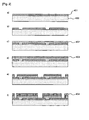
- FIGS. 1 and 2 are cross-sectional views of a structure of a solar cell showing a method for manufacturing a thin-film type solar cell according to one embodiment of the present invention by each process, respectively.
- FIG. 1 is a cross-sectional view of a stacking structure of devices showing a method for manufacturing a thin-film type solar cell according to one embodiment of the present invention by each process.
- the following processes are only one example embodiment and may not be limited to this particular sequence.
- Step (a) is an initial step for manufacturing a thin-film type solar cell of the present invention.
- a lower transparent electrode layer 301 is deposited on a substrate 300.
- a semiconductor layer 302 for photoelectric conversion is deposited on the lower transparent electrode layer 301.
- semiconductor materials that convert light energy into electric energy, can be used.
- any one may be selected from a group consisting of amorphous silicon, microcrystalline silicon, single crystal silicon, polysilicon, amorphous SiC, amorphous SiN, amorphous SiGe, amorphous SiSn, gallium arsenide (GaAs), aluminum gallium arsenide (AIGaAs), indium phosphide (InP), gallium phosphide (GaP), Copper Indium Gallium Selenide (CIGS), cadmium telluride (CdTe), cadmium sulfide (CdS), copper(I) sulfide (Cu 2 S), zinc telluride (ZnTe), lead sulphide (PbS), copper indium diselenide (CulnSe 2
- step (C) an upper transparent electrode layer 303 is deposited on the semiconductor layer 302 for photoelectric conversion.
- step (d) portions of the lower transparent electrode layer 301, the semiconductor layer 302 for photoelectric conversion, and the upper transparent electrode layer 303 are cut through so that portions of the substrate 300 are exposed.
- the solar cell is divided into a plurality of solar cells (unit cells, or unit solar cells) by the cutting process.
- the lower transparent electrode layer 301 and the upper transparent electrode layer 303 are referenced according to the positions they occupy in each of the stacked solar cell devices shown in a cross-sectional view for convenience sake. They can be deposited using the same materials and methods. They can be deposited by a known deposition method using materials usable as a conductive layer known to those skilled in the art. In particular, tin oxide (SnO 2 ) and indium tin oxide (ITO), which are materials having good conductivity, are preferably used.
- the cutting process in the related art known to those skilled in the art can be used.
- the cutting process can be any one of an optical scribing method, a mechanical scribing method, a plasma based etching method, a wet etching method, a dry etching method, a lift-off method, and/or a wire mask method.
- the laser scribing method is a method that diagonally scans laser light with respect to a substrate and processes a thin film on the substrate.
- step (e) the laser scribing on the semiconductor layer 302 for photoelectric conversion and the upper transparent electrode layer 303 is performed so that a portion of the lower transparent electrode layer 301 is exposed.
- steps (d) and (e) the continuous cutting is performed, such that a hard scribing technology can be smoothly performed.
- the size of the exposed substrate and the lower transparent electrode layer is not limited, but the size will be enough to classify or delineate the plurality of solar cells.
- step (f) an insulating layer 304 is directly printed on the lower transparent electrode layer 301 in a cell unit, and side exposed parts of the semiconductor layer 302 for photoelectric conversion and the upper transparent electrode layer 303 to isolate each of the plurality of solar cells.
- a direct printing method used in the present invention may include a screen printing method, an offset lithography printing method, an inkjet printing method, a roll-to-roll method, etc.
- the thin-film type solar cell can be mass produced by these technologies.
- the screen printing method which is a non-pressing printing method using stencil, has an advantage in that ink and the substrate are not affected. As a result, it is appropriate for thickly depositing ink on a large-area substrate. Further, the screen printing method is a technology that can perform a thin film forming process and a patterning process in the atmosphere at one time.
- the offset lithography printing method which is a process technology that can print various kinds of materials, is a technology using a suction condition arising from a substrate surface energy.
- the inkjet printing method which is a technology that forms fine ink drops and patterns them on desired positions on the substrate and is a non-contact scheme, is suitable for implementing a complicated shape in a small volume.
- the insulating layer 304 is composed of one or more materials selected from a group consisting of an oxide and a nitride.
- a rear electrode layer 305 is directly printed on the plurality of cells to connect the upper transparent layer 303 and a portion of the exposed lower transparent electrode layer 301 in series.
- the divided cells are connected to each other in series by the rear electrode layer 305 to form a solar cell module on the substrate.
- the cells are connected to each other while (or by) forming the rear electrode layer 305 of the cell.
- the rear electrode layer 305 can be also processed in simpler and easier processes using the direct printing method as described above.
- the rear electrode layer 305 composed of metallic materials such as aluminum, etc.
- the screen printing method the offset lithography printing method, the inkjet printing method, the roll-to-roll method, etc., such that the solar cell can be mass produced, making it possible to obtain an effect of cost reduction.
- the rear electrode layer 305 can be formed using the materials that can generally be used for the electrode layer and methods, which are known to those skilled in the art.
- a metal layer composed of aluminum (Al), silver (Ag), titanium (Ti), palladium (Pd), etc. is manufactured using the screen printing method.
- the manufacturing of the metal layer uses a method that performs the screen printing with Ag paste, stabilizes it, dries it in an oven, and then performs heat treatment thereon.
- the method for manufacturing a thin-film type solar cell according to one embodiment of the present invention as described above has a process in that the printing process should be performed twice, but has an advantage in that after all the deposition processes are performed from the lower transparent electrode layer, the scribing process and the printing process can be performed separately.
- the thin-film type solar cell manufactured using the method for manufacturing a solar cell of FIG. 1 is configured of the plurality of unit cells divided by the patterning and these unit cells are electrically connected to each other by the transparent conductive layers formed on upper and lower portions of the photoelectric conversion layer of each solar cell.
- the plurality of unit cells are electrically connected to each other in series, making it possible to configure an integrated thin-film type solar cell.
- the insulating layer 304 is disposed between the unit cells, which prevents the upper and lower transparent electrode layers 303, 301 inside one unit solar cell from electrically connecting each other, and can connect the upper and lower transparent electrode layers 303, 301 to the adjacent unit solar cells in series.
- the thin-film type solar cell is patterned into the plurality of cells by sequentially performing the cutting process on the upper transparent electrode layer 303, the semiconductor layer 302 for photoelectric conversion, and the lower transparent electrode layer 301 from the top.
- the insulating layer 304 is formed between the plurality of cells and the rear electrode layer 305 is formed thereon, making it possible to form a structure where the adjacent unit cells are electrically connected to each other.
- FIG. 2 is a cross-sectional view of a stacking structure of devices which shows a method for manufacturing a thin-film type solar cell according to one embodiment of the present invention by each process.
- Step (a) is an initial step for manufacturing a thin-film type solar cell of the present invention.
- a lower transparent electrode layer 401 is deposited on a substrate 400.
- the deposition process selected from the thin film deposition methods known to those skilled in the art can be used.
- step (b) the laser scribing on the lower transparent electrode layer 401 is performed so that a portion of the substrate 400 is exposed.
- step (c) a semiconductor layer 402 for photoelectric conversion is deposited on the lower transparent electrode layer 401 that is subjected to the laser scribing.
- the materials usable for the semiconductor layer 302 for photoelectric conversion as described above can also be used for the semiconductor layer 402 in the present embodiment.
- step (d) an upper transparent electrode layer 403 is deposited on the semiconductor layer 402 for photoelectric conversion.
- step (e) the semiconductor layer 402 for photoelectric conversion and the upper transparent electrode layer 403 are cut so that a portion of the lower transparent electrode layer 401 is exposed.
- the plurality of unit solar cells can be formed through these cutting processes. The cutting process is the same as the foregoing embodiment.
- the lower transparent electrode layer 401 and the upper transparent electrode layer 403 can use the same materials as the lower transparent electrode layer 301 and the upper transparent electrode layer 303 described in the foregoing embodiment.
- step (f) the direct printing is performed on the rear electrode layer 404 to connect the upper transparent electrode layer 403 of the predetermined cell and the lower transparent electrode layer 401 of a cell adjacent thereto in series.
- the cells are connected to each other while (or by) forming the rear electrode layer 404 of the cell.
- the rear electrode layer 404 can use the same materials as the rear electrode layer 305 of the foregoing embodiment.
- the direct printing method is the same as the foregoing description.
- the thin-film type solar cell manufactured through the method for manufacturing a solar cell shown in FIG. 2 is manufactured through a two-step process that saves the cutting process once, unlike the method for manufacturing a solar cell according to the related art.
- the thin film solar cell is patterned into the plurality of cells by sequentially performing a secondary cutting process on the upper transparent electrode layer 403 and the semiconductor layer 402 for photoelectric conversion from the top to meet the pattern.
- the rear electrode layer 404 is simply and easily formed on the plurality of cells by the direct printing method as in the embodiment of FIG. 1 , such that the adjacent unit cells are electrically connected to each other.
- the above embodiment controls the inter-layer structure by the patterning using the cutting process and the sequence of deposition within the manufacturing method according to the present invention, such that the above structure can be achieved without adding a separate process, thereby facilitating the manufacturing of the thin-film type solar cell. Further, the frequency of the cutting process is reduced as compared to the method for manufacturing a thin-film type solar cell according to the related art, such that the solar cell having high photoelectric conversion efficiency while reducing process costs can be manufactured.
- the method for manufacturing a thin-film type solar cell according to one embodiment of the present invention performs the scribing after the deposition of the lower transparent electrode layer and the deposition and scribing processes again, and then performs the printing, it has a process that is continuous but has an advantage in reducing the number of processes by performing the printing process once.
Abstract
Description
- The present invention relates to a thin-film type solar cell and a method for manufacturing the same, and more specifically, to a method for manufacturing a thin-film type solar cell having high photoelectric conversion efficiency while reducing process costs by reducing a frequency of a patterning process. Further, the present invention relates to a method for manufacturing a thin-film type solar cell in which a rear electrode layer is simply formed using a direct printing method in the process of sequentially forming a lower transparent electrode layer, a semiconductor layer for photoelectric conversion, and an upper transparent electrode layer on a substrate and forming each rear electrode layer after patterning into a plurality of cells.
- Recently, eco-friendly alternative energy is getting more and more interest due to an earth environment problem and a resource depletion problem. Under this situation, one of technologies in which people are focusing attention is a photovoltaic generation technology. A solar cell to generate electricity using sunlight has generally been manufactured using silicon. Currently commercialized bulk silicon solar cells have not entered into widespread use due to high manufacturing costs and installation costs. In order to solve such problems related to the cost, research into a thin-film type solar cell using silicon has activelyprogressed and various attempts to manufacture a high efficiency solar cell module have been made.
- The solar cell is a next-generation clean energy source and much research thereinto has been underway for several decades. As materials used for the solar cell, materials of group IV, such as single crystal silicon, polycrystalline silicon, amorphous silicon, amorphous SiC, amorphous SiN, amorphous SiGe, amorphous SiSn, etc., and compound semiconductors of group III-V, such as GaAs, AlGaAs, InP, etc. or group II-VI of CdS, CdTe, Cu2S , etc. have been used.
- Generally, a solar cell should have the following characteristics: high photoelectric conversion efficiency, low manufacturing costs, short energy recovery period, etc. In particular, since a reduction in process frequency is economically useful in terms of the manufacturing costs of the solar cell, research into this field has actively progressed.
- Accordingly, it is an object of the present invention to provide a thin-film type solar cell having high photoelectric conversion efficiency by a relatively simple process and a method for manufacturing solar cell devices at low manufacturing costs, in a thin-film type solar cell.
- In particular, it is another object of the present invention to provide a method for manufacturing solar cell devices capable of reducing a patterning frequency to minimize a dead area occurring in a patterning process, thereby improving efficiency and removing metal electrode residues to improve process reliability.
- In order to achieve the objects, there is provided a method for manufacturing a thin-film solar cell including sequentially forming a lower transparent electrode layer, a semiconductor layer for photoelectric conversion, and an upper transparent electrode layer on a substrate; cutting through portions of the lower transparent electrode layer, the semiconductor layer for photoelectric conversion, and the upper transparent electrode layer, so that a plurality cells are patterned, and portions of the substrate and other portions of the lower transparent electrode layer are simultaneously exposed; forming an insulating layer on the plurality of cells so that respective portions of the insulating layer extend between a lower transparent electrode layer and an upper transparent electrode layer of each of the plurality of cells; and forming a rear electrode layer on the plurality of cells so that respective portions of the rear electrode layer extend to connect an upper transparent electrode layer of one of the plurality of cells to a lower transparent electrode layer of an adjacent another of the plurality of cells in series.
- There is also provided a method for manufacturing a thin-film solar cell, including cutting through portions of a lower transparent electrode layer formed on a substrate to pattern the lower transparent electrode layer; sequentially forming a semiconductor layer for photoelectric conversion and an upper transparent electrode layer on the patterned lower transparent electrode layer; cutting through portions of the semiconductor layer for photoelectric conversion and the transparent electrode layer to pattern a plurality of cells and to expose other portions of the lower transparent electrode layer; and forming a rear electrode layer on the plurality of cells so that respective portions of the rear electrode extend to connect an upper transparent electrode layer of one of the plurality of cells and a portion of an exposed lower transparent electrode layer of an adjacent another of the plurality of cells in series.
- There is also provided a thin-film solar cell including a plurality of cells, the thin-film solar cell including a substrate; and a lower transparent layer, a semiconductor layer for photoelectric conversion, an upper transparent layer, and a rear electrode layer that are sequentially formed on the substrate, wherein respective portions of the rear electrode layer extend from an upper surface of the upper transparent electrode layer of one of the plurality of cells to a lower transparent electrode layer of an adjacent another of the plurality of cells in series.
- In the manufacturing process of a solar cell according to the related art, a portion lost by the cutting process is 100 m or more. However, the method for manufacturing a solar cell according to the present invention reduces the frequency of the cutting process to increase the cost reducing effect in terms of manufacturing costs and provide a solar cell through simpler process. In other words, in manufacturing the thin-film type solar cell, the manufacturing method according to the related art needs to perform the cutting process numerous times. However, the present invention reduces the cutting process over the related art, as well as similar processes are simultaneously performed to unify the process to promote simplification and unification in terms of the manufacturing process, making it possible to manufacture the thin-film type solar cell with reduced manufacturing costs.
- According to the present invention, the thin-film type solar cell can be manufactured at one time through a series of manufacturing processes that results in high photoelectric conversion efficiency and is relatively simple. Further, the present invention can manufacture the solar cell by reducing the frequency of patterning and the process costs.
- The present invention proposes the structure and method for manufacturing the solar cell that has the high photoelectric conversion efficiency and can be manufactured at a reduced process costs. As a result, when the present invention is commercialized, the commercialized solar cell as the next-generation clean energy source contributes to the earth environment as well as may be directly applied for various fields such as public facilities, private facilities, military facilities, etc., making it possible to create a huge economic value.
- The above objects, features and advantages of the present invention will become more apparent to those skilled in the art in conjunction with the accompanying drawings. In the drawings:
-
FIGS. 1 and2 are cross-sectional views of a structure of a solar cell showing a method for manufacturing a thin-film type solar cell according to one embodiment of the present invention by each process, respectively. - Hereinafter, example embodiments of the present invention will be described in detail with reference to the accompanying drawings. In referring to reference numerals to components of each drawing, the same components are referred to by the same reference numerals as much as possible even if they are shown in different figures. Detailed descriptions of well-known techniques are omitted so as not to obscure the description of the present invention with unnecessary detail.
-
FIG. 1 is a cross-sectional view of a stacking structure of devices showing a method for manufacturing a thin-film type solar cell according to one embodiment of the present invention by each process. The following processes are only one example embodiment and may not be limited to this particular sequence. - The processes will be described in detail with reference to
FIG. 1 . Step (a) is an initial step for manufacturing a thin-film type solar cell of the present invention. In detail, a lowertransparent electrode layer 301 is deposited on asubstrate 300. - In step (b), a
semiconductor layer 302 for photoelectric conversion is deposited on the lowertransparent electrode layer 301. As materials used for thesemiconductor layer 302 for photoelectric conversion, semiconductor materials, that convert light energy into electric energy, can be used. For example, any one may be selected from a group consisting of amorphous silicon, microcrystalline silicon, single crystal silicon, polysilicon, amorphous SiC, amorphous SiN, amorphous SiGe, amorphous SiSn, gallium arsenide (GaAs), aluminum gallium arsenide (AIGaAs), indium phosphide (InP), gallium phosphide (GaP), Copper Indium Gallium Selenide (CIGS), cadmium telluride (CdTe), cadmium sulfide (CdS), copper(I) sulfide (Cu2S), zinc telluride (ZnTe), lead sulphide (PbS), copper indium diselenide (CulnSe2;CIS), gallium-antimonide(GaSb), and compounds thereof. - In step (C), an upper
transparent electrode layer 303 is deposited on thesemiconductor layer 302 for photoelectric conversion. - In step (d), portions of the lower
transparent electrode layer 301, thesemiconductor layer 302 for photoelectric conversion, and the uppertransparent electrode layer 303 are cut through so that portions of thesubstrate 300 are exposed. The solar cell is divided into a plurality of solar cells (unit cells, or unit solar cells) by the cutting process. - The lower
transparent electrode layer 301 and the uppertransparent electrode layer 303 are referenced according to the positions they occupy in each of the stacked solar cell devices shown in a cross-sectional view for convenience sake. They can be deposited using the same materials and methods. They can be deposited by a known deposition method using materials usable as a conductive layer known to those skilled in the art. In particular, tin oxide (SnO2) and indium tin oxide (ITO), which are materials having good conductivity, are preferably used. - Further, the cutting process in the related art known to those skilled in the art can be used. Generally, the cutting process can be any one of an optical scribing method, a mechanical scribing method, a plasma based etching method, a wet etching method, a dry etching method, a lift-off method, and/or a wire mask method.
- Meanwhile, as the optical scribing method, a laser scribing method is mainly used. The laser scribing method is a method that diagonally scans laser light with respect to a substrate and processes a thin film on the substrate.
- Next, in step (e), the laser scribing on the
semiconductor layer 302 for photoelectric conversion and the uppertransparent electrode layer 303 is performed so that a portion of the lowertransparent electrode layer 301 is exposed. In steps (d) and (e), the continuous cutting is performed, such that a hard scribing technology can be smoothly performed. - The size of the exposed substrate and the lower transparent electrode layer is not limited, but the size will be enough to classify or delineate the plurality of solar cells.
- In step (f), an
insulating layer 304 is directly printed on the lowertransparent electrode layer 301 in a cell unit, and side exposed parts of thesemiconductor layer 302 for photoelectric conversion and the uppertransparent electrode layer 303 to isolate each of the plurality of solar cells. - A direct printing method used in the present invention may include a screen printing method, an offset lithography printing method, an inkjet printing method, a roll-to-roll method, etc. The thin-film type solar cell can be mass produced by these technologies.
- Meanwhile, the screen printing method, which is a non-pressing printing method using stencil, has an advantage in that ink and the substrate are not affected. As a result, it is appropriate for thickly depositing ink on a large-area substrate. Further, the screen printing method is a technology that can perform a thin film forming process and a patterning process in the atmosphere at one time.
- The offset lithography printing method, which is a process technology that can print various kinds of materials, is a technology using a suction condition arising from a substrate surface energy.
- The inkjet printing method, which is a technology that forms fine ink drops and patterns them on desired positions on the substrate and is a non-contact scheme, is suitable for implementing a complicated shape in a small volume.
- Additionally, the insulating
layer 304 is composed of one or more materials selected from a group consisting of an oxide and a nitride. - In step (g), a
rear electrode layer 305 is directly printed on the plurality of cells to connect the uppertransparent layer 303 and a portion of the exposed lowertransparent electrode layer 301 in series. Through this process, the divided cells are connected to each other in series by therear electrode layer 305 to form a solar cell module on the substrate. In other words, the cells are connected to each other while (or by) forming therear electrode layer 305 of the cell. - The
rear electrode layer 305 can be also processed in simpler and easier processes using the direct printing method as described above. - In other words, the
rear electrode layer 305 composed of metallic materials such as aluminum, etc., can be easily formed by the screen printing method, the offset lithography printing method, the inkjet printing method, the roll-to-roll method, etc., such that the solar cell can be mass produced, making it possible to obtain an effect of cost reduction. - The
rear electrode layer 305 can be formed using the materials that can generally be used for the electrode layer and methods, which are known to those skilled in the art. In particular, a metal layer composed of aluminum (Al), silver (Ag), titanium (Ti), palladium (Pd), etc., is manufactured using the screen printing method. Generally, the manufacturing of the metal layer uses a method that performs the screen printing with Ag paste, stabilizes it, dries it in an oven, and then performs heat treatment thereon. - The method for manufacturing a thin-film type solar cell according to one embodiment of the present invention as described above has a process in that the printing process should be performed twice, but has an advantage in that after all the deposition processes are performed from the lower transparent electrode layer, the scribing process and the printing process can be performed separately.
- The thin-film type solar cell manufactured using the method for manufacturing a solar cell of
FIG. 1 is configured of the plurality of unit cells divided by the patterning and these unit cells are electrically connected to each other by the transparent conductive layers formed on upper and lower portions of the photoelectric conversion layer of each solar cell. The plurality of unit cells are electrically connected to each other in series, making it possible to configure an integrated thin-film type solar cell. - Upon connecting the unit cells in series, the insulating
layer 304 is disposed between the unit cells, which prevents the upper and lowertransparent electrode layers transparent electrode layers - In other words, in one embodiment of the present invention, the thin-film type solar cell is patterned into the plurality of cells by sequentially performing the cutting process on the upper
transparent electrode layer 303, thesemiconductor layer 302 for photoelectric conversion, and the lowertransparent electrode layer 301 from the top. The insulatinglayer 304 is formed between the plurality of cells and therear electrode layer 305 is formed thereon, making it possible to form a structure where the adjacent unit cells are electrically connected to each other. -
FIG. 2 is a cross-sectional view of a stacking structure of devices which shows a method for manufacturing a thin-film type solar cell according to one embodiment of the present invention by each process. - The processes will be described in detail with reference to
FIG. 2 . Step (a) is an initial step for manufacturing a thin-film type solar cell of the present invention. In detail, a lowertransparent electrode layer 401 is deposited on asubstrate 400. The deposition process selected from the thin film deposition methods known to those skilled in the art can be used. - In step (b), the laser scribing on the lower
transparent electrode layer 401 is performed so that a portion of thesubstrate 400 is exposed. In step (c), asemiconductor layer 402 for photoelectric conversion is deposited on the lowertransparent electrode layer 401 that is subjected to the laser scribing. - The materials usable for the
semiconductor layer 302 for photoelectric conversion as described above can also be used for thesemiconductor layer 402 in the present embodiment. - In step (d), an upper
transparent electrode layer 403 is deposited on thesemiconductor layer 402 for photoelectric conversion. In step (e), thesemiconductor layer 402 for photoelectric conversion and the uppertransparent electrode layer 403 are cut so that a portion of the lowertransparent electrode layer 401 is exposed. The plurality of unit solar cells can be formed through these cutting processes. The cutting process is the same as the foregoing embodiment. - The lower
transparent electrode layer 401 and the uppertransparent electrode layer 403 can use the same materials as the lowertransparent electrode layer 301 and the uppertransparent electrode layer 303 described in the foregoing embodiment. - In step (f), the direct printing is performed on the
rear electrode layer 404 to connect the uppertransparent electrode layer 403 of the predetermined cell and the lowertransparent electrode layer 401 of a cell adjacent thereto in series. In other words, the cells are connected to each other while (or by) forming therear electrode layer 404 of the cell. - The
rear electrode layer 404 can use the same materials as therear electrode layer 305 of the foregoing embodiment. The direct printing method is the same as the foregoing description. - The thin-film type solar cell manufactured through the method for manufacturing a solar cell shown in
FIG. 2 is manufactured through a two-step process that saves the cutting process once, unlike the method for manufacturing a solar cell according to the related art. The thin film solar cell is patterned into the plurality of cells by sequentially performing a secondary cutting process on the uppertransparent electrode layer 403 and thesemiconductor layer 402 for photoelectric conversion from the top to meet the pattern. Therear electrode layer 404 is simply and easily formed on the plurality of cells by the direct printing method as in the embodiment ofFIG. 1 , such that the adjacent unit cells are electrically connected to each other. - The above embodiment controls the inter-layer structure by the patterning using the cutting process and the sequence of deposition within the manufacturing method according to the present invention, such that the above structure can be achieved without adding a separate process, thereby facilitating the manufacturing of the thin-film type solar cell. Further, the frequency of the cutting process is reduced as compared to the method for manufacturing a thin-film type solar cell according to the related art, such that the solar cell having high photoelectric conversion efficiency while reducing process costs can be manufactured.
- Further, since the method for manufacturing a thin-film type solar cell according to one embodiment of the present invention as described above performs the scribing after the deposition of the lower transparent electrode layer and the deposition and scribing processes again, and then performs the printing, it has a process that is continuous but has an advantage in reducing the number of processes by performing the printing process once.
- Although the present invention has been described in connection with the exemplary embodiments illustrated in the drawings, it is only illustrative. It will be understood by those skilled in the art that various modifications and equivalents can be made to the present invention. Therefore, the true technical scope of the present invention should be defmed by the appended claims.
Claims (5)
- A method for manufacturing a thin-film solar cell, comprising:cutting through portions of a lower transparent electrode layer formed on a substrate to pattern the lower transparent electrode layer;sequentially forming a semiconductor layer for photoelectric conversion and an upper transparent electrode layer on the patterned lower transparent electrode layer;cutting through portions of the semiconductor layer for photoelectric conversion and the transparent electrode layer, so that a plurality of cells are patterned, andportions of the lower transparent electrode layer are exposed; andforming a rear electrode layer on the plurality of cells so that respective portions of the rear electrode layer extend to connect an upper transparent electrode layer of one of the plurality of cells and a portion of an exposed lower transparent electrode layer of an adjacent another of the plurality of cells in series.
- The method according to claim 1, wherein the rear electrode layer is formed by a direct printing method.
- The method according to claim 2, wherein the direct printing method is any one of a screen printing method, an offset lithography printing method, and an inkjet printing method.
- The method according to any one of claims 1 to 3, wherein a method for at least one of the two cutting through steps is at least one of a laser scribing method, a mechanical scribing method, a plasma based etching method, a wet etching method, a dry etching method, a lift-off method, and a wire mask method.
- A thin-film solar cell including a plurality of cells, the thin-film solar cell comprising:a substrate; anda lower transparent layer, a semiconductor layer for photoelectric conversion, an upper transparent layer, and a rear electrode layer that are sequentially formed on the substrate, wherein respective portions of the rear electrode layer extend from an upper surface of the upper transparent electrode layer of one of the plurality of cells to a lower transparent electrode layer of an adjacent another of the plurality of cells in series, wherein portions of the substrate are exposed, and respective portions of the semiconductor layer for photoelectric conversion are provided in the respective exposed portions of the substrate between adjacent portions of the lower transparent electrode layer of the plurality of cells.
Applications Claiming Priority (2)
| Application Number | Priority Date | Filing Date | Title |
|---|---|---|---|
| KR1020080085820A KR101144808B1 (en) | 2008-09-01 | 2008-09-01 | Manufacturing Method For Thin-Film Type Solar Cell And The Same thereof |
| EP09810241A EP2332178A4 (en) | 2008-09-01 | 2009-08-31 | Thin-film type solar cell and method for manufacturing the same |
Related Parent Applications (1)
| Application Number | Title | Priority Date | Filing Date |
|---|---|---|---|
| EP09810241.1 Division | 2009-08-31 |
Publications (1)
| Publication Number | Publication Date |
|---|---|
| EP2573813A1 true EP2573813A1 (en) | 2013-03-27 |
Family
ID=41722156
Family Applications (2)
| Application Number | Title | Priority Date | Filing Date |
|---|---|---|---|
| EP09810241A Ceased EP2332178A4 (en) | 2008-09-01 | 2009-08-31 | Thin-film type solar cell and method for manufacturing the same |
| EP12008455A Withdrawn EP2573813A1 (en) | 2008-09-01 | 2009-08-31 | Method of manufacturing a thin film solar cell with unit cells connected in series with a reduced number of patterning steps and corresponding device |
Family Applications Before (1)
| Application Number | Title | Priority Date | Filing Date |
|---|---|---|---|
| EP09810241A Ceased EP2332178A4 (en) | 2008-09-01 | 2009-08-31 | Thin-film type solar cell and method for manufacturing the same |
Country Status (4)
| Country | Link |
|---|---|
| US (1) | US20100059100A1 (en) |
| EP (2) | EP2332178A4 (en) |
| KR (1) | KR101144808B1 (en) |
| WO (1) | WO2010024636A2 (en) |
Cited By (1)
| Publication number | Priority date | Publication date | Assignee | Title |
|---|---|---|---|---|
| PL422635A1 (en) * | 2017-08-25 | 2019-03-11 | Eos Spółka Z Ograniczoną Odpowiedzialnością | Method for manufacturing a photovoltaic component and the photovoltaic component |
Families Citing this family (11)
| Publication number | Priority date | Publication date | Assignee | Title |
|---|---|---|---|---|
| JP2011066045A (en) * | 2009-09-15 | 2011-03-31 | Seiko Epson Corp | Method for manufacturing solar cell |
| KR101210168B1 (en) * | 2010-03-24 | 2012-12-07 | 엘지이노텍 주식회사 | Solar cell apparatus and method of fabricating the same |
| US8563351B2 (en) * | 2010-06-25 | 2013-10-22 | Taiwan Semiconductor Manufacturing Co., Ltd. | Method for manufacturing photovoltaic device |
| WO2012030701A2 (en) * | 2010-08-30 | 2012-03-08 | First Solar, Inc. | Photovoltaic device interconnect |
| KR20130109330A (en) * | 2012-03-27 | 2013-10-08 | 엘지이노텍 주식회사 | Solar cell and method of fabricating the same |
| KR101301003B1 (en) * | 2012-04-30 | 2013-08-28 | 에스엔유 프리시젼 주식회사 | Method for manufacturing thin film solar cell and thin film solar cell using the same |
| US9306106B2 (en) | 2012-12-18 | 2016-04-05 | International Business Machines Corporation | Monolithic integration of heterojunction solar cells |
| CN103984768B (en) | 2014-05-30 | 2017-09-29 | 华为技术有限公司 | A kind of data-base cluster manages method, node and the system of data |
| KR102423108B1 (en) * | 2015-06-11 | 2022-07-22 | 주성엔지니어링(주) | Thin film type solar cell and method for manufacturing the same |
| KR101868792B1 (en) * | 2016-08-05 | 2018-06-19 | 박준형 | Rechargeable display panel by self power generation |
| JP6592639B1 (en) * | 2018-03-23 | 2019-10-16 | 積水化学工業株式会社 | SOLAR CELL MANUFACTURING METHOD AND SOLAR CELL |
Citations (6)
| Publication number | Priority date | Publication date | Assignee | Title |
|---|---|---|---|---|
| JPH0381647U (en) * | 1989-12-08 | 1991-08-21 | ||
| EP0749161A2 (en) * | 1995-06-15 | 1996-12-18 | Kanegafuchi Kagaku Kogyo Kabushiki Kaisha | Integrated thin-film solar battery and method of manufacturing the same |
| EP1116699A1 (en) * | 1998-09-04 | 2001-07-18 | Nippon Sheet Glass Co., Ltd. | Light-colored glass of high transmittance and method for production thereof, glass plate with electrically conductive film and method for production thereof, and glass article |
| JP2002217436A (en) * | 2001-01-22 | 2002-08-02 | Sanyo Electric Co Ltd | Manufacture of integrated photovoltaic device |
| WO2008030019A1 (en) * | 2006-09-04 | 2008-03-13 | Lg Electronics Inc. | Thin-film type solar cell including by-pass diode and manufacturing method thereof |
| EP1962331A2 (en) * | 2007-02-26 | 2008-08-27 | LG Electronics Inc. | Thin-film solar cell and method of manufacturing the same |
Family Cites Families (11)
| Publication number | Priority date | Publication date | Assignee | Title |
|---|---|---|---|---|
| JP60041878B2 (en) * | 1979-02-14 | 1985-09-19 | Sharp Kk | Thin film solar cell |
| GB2179748B (en) * | 1985-08-20 | 1989-09-06 | Sharp Kk | Thermal flow sensor |
| JP2986875B2 (en) * | 1990-09-07 | 1999-12-06 | キヤノン株式会社 | Integrated solar cell |
| AU8872891A (en) * | 1990-10-15 | 1992-05-20 | United Solar Systems Corporation | Monolithic solar cell array and method for its manufacture |
| EP1045454A4 (en) * | 1998-07-27 | 2001-10-24 | Citizen Watch Co Ltd | Solar cell and method of producing the same, and mask for photolithography for producing solar cell |
| US6617798B2 (en) * | 2000-03-23 | 2003-09-09 | Samsung Sdi Co., Ltd. | Flat panel display device having planar field emission source |
| EP1593163B1 (en) * | 2003-01-30 | 2015-06-17 | PST Sensors (Pty) Limited | A thin film semiconductor device and method of manufacturing a thin film semiconductor device |
| JP2006013403A (en) * | 2004-06-29 | 2006-01-12 | Sanyo Electric Co Ltd | Solar cell, solar cell module, its manufacturing method, and its reparing method |
| US20070079866A1 (en) * | 2005-10-07 | 2007-04-12 | Applied Materials, Inc. | System and method for making an improved thin film solar cell interconnect |
| US7547570B2 (en) * | 2006-03-31 | 2009-06-16 | Applied Materials, Inc. | Method for forming thin film photovoltaic interconnects using self-aligned process |
| EP2054927A1 (en) * | 2006-08-22 | 2009-05-06 | Timothy Michael Walsh | Thin-film solar module |
-
2008
- 2008-09-01 KR KR1020080085820A patent/KR101144808B1/en not_active IP Right Cessation
-
2009
- 2009-08-31 EP EP09810241A patent/EP2332178A4/en not_active Ceased
- 2009-08-31 WO PCT/KR2009/004871 patent/WO2010024636A2/en active Application Filing
- 2009-08-31 EP EP12008455A patent/EP2573813A1/en not_active Withdrawn
- 2009-09-01 US US12/552,008 patent/US20100059100A1/en not_active Abandoned
Patent Citations (6)
| Publication number | Priority date | Publication date | Assignee | Title |
|---|---|---|---|---|
| JPH0381647U (en) * | 1989-12-08 | 1991-08-21 | ||
| EP0749161A2 (en) * | 1995-06-15 | 1996-12-18 | Kanegafuchi Kagaku Kogyo Kabushiki Kaisha | Integrated thin-film solar battery and method of manufacturing the same |
| EP1116699A1 (en) * | 1998-09-04 | 2001-07-18 | Nippon Sheet Glass Co., Ltd. | Light-colored glass of high transmittance and method for production thereof, glass plate with electrically conductive film and method for production thereof, and glass article |
| JP2002217436A (en) * | 2001-01-22 | 2002-08-02 | Sanyo Electric Co Ltd | Manufacture of integrated photovoltaic device |
| WO2008030019A1 (en) * | 2006-09-04 | 2008-03-13 | Lg Electronics Inc. | Thin-film type solar cell including by-pass diode and manufacturing method thereof |
| EP1962331A2 (en) * | 2007-02-26 | 2008-08-27 | LG Electronics Inc. | Thin-film solar cell and method of manufacturing the same |
Cited By (1)
| Publication number | Priority date | Publication date | Assignee | Title |
|---|---|---|---|---|
| PL422635A1 (en) * | 2017-08-25 | 2019-03-11 | Eos Spółka Z Ograniczoną Odpowiedzialnością | Method for manufacturing a photovoltaic component and the photovoltaic component |
Also Published As
| Publication number | Publication date |
|---|---|
| EP2332178A2 (en) | 2011-06-15 |
| KR20100026710A (en) | 2010-03-10 |
| EP2332178A4 (en) | 2012-06-06 |
| WO2010024636A2 (en) | 2010-03-04 |
| KR101144808B1 (en) | 2012-05-11 |
| WO2010024636A3 (en) | 2010-06-24 |
| US20100059100A1 (en) | 2010-03-11 |
Similar Documents
| Publication | Publication Date | Title |
|---|---|---|
| EP2573813A1 (en) | Method of manufacturing a thin film solar cell with unit cells connected in series with a reduced number of patterning steps and corresponding device | |
| JP6055787B2 (en) | Solar cell and manufacturing method thereof | |
| KR20070101917A (en) | Thin-film solar cell and fabrication method thereof | |
| US20130244373A1 (en) | Solar cell apparatus and method of fabricating the same | |
| EP2426731A2 (en) | Solar power generation apparatus and manufacturing method thereof | |
| JP2013510426A (en) | Solar cell and manufacturing method thereof | |
| KR20110035715A (en) | Solar cell and method of fabircating the same | |
| EP2538454A1 (en) | Device for generating solar power and method for manufacturing same | |
| JP2013506987A (en) | Photovoltaic power generation apparatus and manufacturing method thereof | |
| JP6034791B2 (en) | Solar power plant | |
| EP2450963A2 (en) | Solar cell and method for producing same | |
| KR101114018B1 (en) | Solar cell and method of fabricating the same | |
| KR101428146B1 (en) | Solar cell module and method of fabricating the same | |
| EP2600422A2 (en) | Device for generating photovoltaic power and manufacturing method for same | |
| KR20110080663A (en) | Solar cell apparatus | |
| TW201517295A (en) | Solar cell and method for manufacturing the same | |
| US20110120534A1 (en) | Thin film solar cell and manufacturing method thereof | |
| JP2013506994A (en) | Photovoltaic power generation apparatus and manufacturing method thereof | |
| KR101028310B1 (en) | Solar cell and method of fabricating the same | |
| KR101338549B1 (en) | Solar cell and method of fabricating the same | |
| KR101172186B1 (en) | Solar cell apparatus and method of fabricating the same | |
| KR101020941B1 (en) | Solar cell and method of fabircating the same | |
| KR102396820B1 (en) | Solar cell module and method of fabricating the same | |
| US20120298169A1 (en) | Multi-junction Photovoltaic Cells | |
| KR101349432B1 (en) | Photovoltaic apparatus and method of fabricating the same |
Legal Events
| Date | Code | Title | Description |
|---|---|---|---|
| PUAI | Public reference made under article 153(3) epc to a published international application that has entered the european phase |
Free format text: ORIGINAL CODE: 0009012 |
|
| AC | Divisional application: reference to earlier application |
Ref document number: 2332178 Country of ref document: EP Kind code of ref document: P |
|
| AK | Designated contracting states |
Kind code of ref document: A1 Designated state(s): AT BE BG CH CY CZ DE DK EE ES FI FR GB GR HR HU IE IS IT LI LT LU LV MC MK MT NL NO PL PT RO SE SI SK SM TR |
|
| 17P | Request for examination filed |
Effective date: 20130925 |
|
| RBV | Designated contracting states (corrected) |
Designated state(s): AT BE BG CH CY CZ DE DK EE ES FI FR GB GR HR HU IE IS IT LI LT LU LV MC MK MT NL NO PL PT RO SE SI SK SM TR |
|
| 17Q | First examination report despatched |
Effective date: 20131125 |
|
| STAA | Information on the status of an ep patent application or granted ep patent |
Free format text: STATUS: THE APPLICATION IS DEEMED TO BE WITHDRAWN |
|
| 18D | Application deemed to be withdrawn |
Effective date: 20140606 |