EP2621024A2 - Contactor, use and method for contacting - Google Patents
Contactor, use and method for contacting Download PDFInfo
- Publication number
- EP2621024A2 EP2621024A2 EP13000449.2A EP13000449A EP2621024A2 EP 2621024 A2 EP2621024 A2 EP 2621024A2 EP 13000449 A EP13000449 A EP 13000449A EP 2621024 A2 EP2621024 A2 EP 2621024A2
- Authority
- EP
- European Patent Office
- Prior art keywords
- component
- circuit board
- contactor
- printed circuit
- connector
- Prior art date
- Legal status (The legal status is an assumption and is not a legal conclusion. Google has not performed a legal analysis and makes no representation as to the accuracy of the status listed.)
- Granted
Links
Images


Classifications
-
- H—ELECTRICITY
- H01—ELECTRIC ELEMENTS
- H01R—ELECTRICALLY-CONDUCTIVE CONNECTIONS; STRUCTURAL ASSOCIATIONS OF A PLURALITY OF MUTUALLY-INSULATED ELECTRICAL CONNECTING ELEMENTS; COUPLING DEVICES; CURRENT COLLECTORS
- H01R12/00—Structural associations of a plurality of mutually-insulated electrical connecting elements, specially adapted for printed circuits, e.g. printed circuit boards [PCB], flat or ribbon cables, or like generally planar structures, e.g. terminal strips, terminal blocks; Coupling devices specially adapted for printed circuits, flat or ribbon cables, or like generally planar structures; Terminals specially adapted for contact with, or insertion into, printed circuits, flat or ribbon cables, or like generally planar structures
- H01R12/70—Coupling devices
- H01R12/71—Coupling devices for rigid printing circuits or like structures
- H01R12/712—Coupling devices for rigid printing circuits or like structures co-operating with the surface of the printed circuit or with a coupling device exclusively provided on the surface of the printed circuit
- H01R12/714—Coupling devices for rigid printing circuits or like structures co-operating with the surface of the printed circuit or with a coupling device exclusively provided on the surface of the printed circuit with contacts abutting directly the printed circuit; Button contacts therefore provided on the printed circuit
-
- H—ELECTRICITY
- H01—ELECTRIC ELEMENTS
- H01R—ELECTRICALLY-CONDUCTIVE CONNECTIONS; STRUCTURAL ASSOCIATIONS OF A PLURALITY OF MUTUALLY-INSULATED ELECTRICAL CONNECTING ELEMENTS; COUPLING DEVICES; CURRENT COLLECTORS
- H01R13/00—Details of coupling devices of the kinds covered by groups H01R12/70 or H01R24/00 - H01R33/00
- H01R13/02—Contact members
- H01R13/22—Contacts for co-operating by abutting
- H01R13/24—Contacts for co-operating by abutting resilient; resiliently-mounted
Definitions
- the present invention relates to a contactor or connector for a component mounted on a printed circuit board, a use of the contactor and a method for contacting the printed circuit board or the component contacted therewith.
- a printed circuit board is understood to be a printed circuit board (also called “PCB” or “printed circuit board”).
- a circuit board may include one or more electrical and / or electronic components such as integrated circuit devices, resistors, capacitors, diodes, transistors, etc., or connectors (connectors, SIMM connectors, post connectors, etc.) .).
- printed circuit boards or integrated circuit components are tested for their functionality after production.
- these are electrically connected to a test board, tested and then removed again.
- the connection of the printed circuit board to the test board can be made in particular by means of a connector of the printed circuit board, which is contacted with a complementary connector of the test board and is decontacted again after the test.
- the number of mating cycles of the complementary connector is limited so that only one test board no series of printed circuit boards can be tested for their functionality.
- a component Under a component are understood active and passive electronic components which are attached or contacted on the circuit board.
- the attachment of the component to the circuit board may preferably be associated with the electrical contacting of the component with the circuit board.
- the component is fastened only or exclusively by means of the connection contacts on the circuit board, for example by soldering.
- the component may alternatively or additionally be attached by means of at least one of the terminal contacts different fastening means to the circuit board, for example by gluing, screwing, clamping, etc.
- the component may preferably be a connector such as a SIMM connector, a DIMM connector, a COM Express connector, and so forth.
- the component can preferably be an integrated circuit component, in particular an SMD component (surface mounted device) or a circuit component which can be contacted in a DFP (dual flat package), a TFP (triple flat package) or a QFP (quad flat package) configuration has.
- the terminal contacts of the component protrude along a direction X 'over the remaining component, for example over a housing of the component or a connector receptacle of the component.
- the direction X ' is substantially perpendicular to a normal of the circuit board to which the component is mounted.
- the direction X ' is oriented substantially parallel to the extension of the circuit board.
- the directions X and X ' are identical.
- the normal of the circuit board may be identical to the insertion direction E.
- the contacting means are preferably arranged in a direction X, which is oriented perpendicular to the insertion direction E, spaced from the component receiving.
- the component receptacle can be arranged between the contacting means.
- the contacting means may at least partially surround the component receptacle.
- the contacting means may form or limit the component receptacle at least in regions.
- the contacting means may be arranged such that the component receptacle adjacent to at least one contact means, that is bounded by this, whereby the distance between the component holder and this or this contacting means (n) is equal to zero.
- the contacting means are preferably arranged in relation to the component receptacle such that the component can be introduced without contact along the insertion direction E into the component receptacle, in particular between the contacting means.
- the contacting means contact only the terminal contacts of the component, which connect the component to the circuit board.
- other elements of the component in the operating position can not be electrically and / or mechanically contacted by the contacting means.
- connection contacts of the component are provided exclusively for electrical or mechanical connection of the component to the printed circuit board and in particular not intended to electrically or mechanically contact the printed circuit board or the component with another external component, such as a complementary connector.
- the component is a connector
- the component has connector contacts which are designed to contact a complementary connector electrically or mechanically.
- Each of the connector contacts in the connector internally connected to an associated with the terminal contacts electrically.
- the contacting elements of the contactor contact electrically and mechanically exclusively the connection contacts.
- the connector contacts are not mechanically contacted by the contacting elements.
- one of the terminal contacts and one of the connector contacts of the component may be integrally formed as a component contact element, wherein the terminal contact describes the region of the component contact element, which is designed to electrically contact the circuit board and the connector contact describes the area of the component contact element, which is designed with to electrically contact an external component.
- the contacting means may be designed to contact in an operating position in each case with a region of the component contact element of the component mounted on the printed circuit board, which is electrically contacted and designed only with the printed circuit board, when the circuit board is used as intended, ie not during the process described in US Pat Not to be contacted with external components electrically or not be contacted.
- the component receptacle may comprise a recess in the Kunststoffor, in which the component along the insertion direction E at least partially inserted.
- the component can in particular also with the exception of the connection contacts be completely acceptable in the component holder, in which case only the terminal contacts projecting against the insertion direction E from the component holder.
- the component in the operating position, may at least partially be in positive engagement with the component receptacle or one or more of the walls thereof.
- the component receiving a spatial displacement of the component along a spatial direction, which is substantially perpendicular to the insertion direction E, be inhibited.
- the component receptacle is at least partially complementarily formed congruent with the male component, so that advantageously by the insertion of the component in the component receiving a positive engagement or a frictional engagement can be formed which inhibits a displacement of the component or the associated circuit board against the insertion direction E.
- the printed circuit board can be held by the component received in the component receptacle.
- merely picking up the component in the component receptacle is sufficient to hold the circuit board at the Kunststoffor in the operating position.
- the operating position therefore describes a position during the operational use of the contactor.
- the contactor has a plurality of contacting means, for example 2, 3, 4, 5, 6, 7, 8, 16, 32, 64, 128, 200, 220, 440, or more contacting means.
- the contacting means are electrically conductive and preferably formed of a metal, in particular of copper, tin, zinc, nickel, silver and alloys containing these metals, such as copper-nickel alloys, bronze and brass.
- the contacting means are resiliently mounted in an associated contacting means receptacle and displaceable along the insertion direction E.
- at least a portion of each contacting means is disposed in an associated contacting means receptacle.
- the contacting means is further, particularly preferably completely, displaceable into the contacting means receptacle.
- the contacting means can in particular be formed from the same material as the contact means.
- the spring-mounted contacting means allow a higher number of possible contacting cycles.
- the contacting means are displaced during the contacting with the terminal contacts along the insertion direction E, so that neither the terminal contacts of the component nor the contacting means are worn or damaged by a mechanical action or by a friction between the terminal contacts and the contacting means.
- resilient mounting the displacement of each contact means is reversible, so that the respective contact means returns after removal of the component from the component holder back to its original position or shape.
- a spring element may preferably be arranged in each contacting means receptacle, which is stretched by displacing the associated contacting means along the insertion direction E, preferably elastically tensioned, so that an elastic restoring force of the spring element can displace the contacting means counter to the insertion direction E.
- the spring element may in particular be formed of the same material as the contact means or the Kunststofftechnischsstofffact.
- the contacting means protrude opposite to the insertion direction E beyond the component receptacle.
- the contacting means can be designed to contact the terminal contacts electrically before the associated component is arranged or inserted in the component receptacle such that the operating position is reached.
- each of the Contacting means by about 0.5 mm to about 5 mm, preferably about 1 mm to about 3 mm, against the insertion direction E protrude beyond the component receiving.
- each of the contacting means is electrically connected to a test board.
- the electrical connection is effected indirectly via the at least one contacting means receptacle and an associated board contact, which is preferably part of the contacting means receptacle or can be formed together with the latter, in particular in one piece.
- the test board may be part of the contactor.
- the component holder is formed at least partially complementary to the male component, so that the recorded component can be fixed by a frictional engagement and / or positive engagement in the component holder.
- the component receptacle can be designed such that only one particular type or several specific types of components can be accommodated by means of the component receptacle. As a result, it can further advantageously be prevented that the contactor or the test board contacted with it contacts with components which are not adequate, whereby the test board or the component to be tested could be damaged.
- the component receptacle can essentially be designed as a complementary connector, wherein it is not necessary to form the connector contacts complementary to the connector contacts of the connector in or on the component receptacle ., Since the contacting of the component does not take place via the component receiving, but by means of the contacting means which contact the terminal contacts of the connector. In order to prevent wear of the connector or the complementary connector, that is, by the insertion of the connector in the component receiving a contacting cycle of the To generate connector or the complementary connector is even excluded that the formed as a complementary connector component receiving also has complementary connector contacts. In other words, complementary connector contacts are contacted electrically and / or mechanically neither by the connector contacts nor by the terminal contacts.
- the contactor comprises a fixing device with which the printed circuit board can be mechanically connected or fastened to the contactor.
- the contactor can comprise latching elements which can engage in the insertion direction with complementary latching elements of the printed circuit board by displacing the printed circuit board along the insertion direction and are latched in the operating position.
- an unintentional loosening or removal of the printed circuit board can be prevented, since to remove the printed circuit board from themaschineor first solved the fixing or the latching elements must be unlocked.
- at least one latching hook may be provided on the contactor, which is latched in the operating position with an edge of the printed circuit board.
- the contactor comprises a straightening device with which the position of the printed circuit board can be aligned relative to the contactor.
- the contactor may comprise at least one projection or at least one pin as a preferred straightening device.
- the straightening device can advantageously ensure the correct insertion of the component into the component receptacle.
- the straightening device can engage with an associated complementary straightening device of the printed circuit board.
- An exemplary complementary straightening device of the printed circuit board may be, for example, a bore or a passage opening in the printed circuit board.
- the contactor comprises at least one component receptacle into which at least one component fastened on the printed circuit board can be inserted at least in regions along the insertion direction E.
- the at least one component is different from the component which is electrically contactable by means of the contacting means.
- an element of the printed circuit board that is to be electrically contacted by the contactor is referred to as a "component”
- an element of the printed circuit board that is merely to be mechanically and / or mechanically contacted, and in particular not electrically contacted is referred to as a "component" becomes.
- Exemplary components of the printed circuit board may be resistors, capacitors, coils, trimmers, diodes, transistors, ICs, connectors, fasteners, etc., which are attached to the circuit board and which could possibly hinder the insertion of the component to be electrically contacted into the component receptacle.
- recesses or depressions along the insertion direction E which are formed in the contactor, allow these interfering components to be accommodated during insertion of the printed circuit board along the insertion direction E in a preferably complementary component receptacle without hindering the insertion.
- the at least one component receptacle can be adapted individually to the circuit board to be tested, so that a confusion of the circuit board to be tested and thus damage to the circuit board or the contactor and the test board connected thereto is prevented.
- One aspect of the present invention relates to the use of a contactor according to the invention for connecting a component mounted on a printed circuit board to a test board, wherein the electrical connection of a each terminal of the component with an associated strigplatinenitch the test board via one of the contacting of the contactor.
- the printed circuit board or the component is thus contacted in a simple manner with the test board, wherein the number of possible contacting cycles is advantageously increased.
- the component can remain on the circuit board, so that a complicated release of the component from the circuit board is not necessary, since the accessible terminal contacts are contacted by means of the contactor electrically.
- the component mounted on the printed circuit board is a connector whose terminal contacts are electrically connected to associated connector contacts, wherein the connector contacts are not contacted or uncontacted by the contacting means in the operative position. Rather, the connector contacts are indirectly electrically connected to the respective associated contacting means via an internal connector electrical connection to the terminal contacts and the terminal contacts themselves.
- testing of the printed circuit board and / or of the component takes place on the printed circuit board.
- the necessary for testing circuit is provided by a test board, which is connected by means of the contactor with the circuit board.
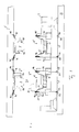
- the FIG. 1 shows a test arrangement 1 comprising a Mixor 3 and a circuit board 5 in a sectional view.
- the FIG. 2 shows the test arrangement 1 of FIG. 1 in an operating position.
- a connector 7 is fixed, wherein the connector 7 has a plurality of terminal contacts 9a, 9b, with which the connector 7 is electrically contacted with the circuit board 5.
- the connector 7 is also mechanically fastened to the printed circuit board 5 by means of the terminal contacts 9a, 9b, for example by soldering the terminal contacts 9a, 9b to associated contact regions 11a, 11b of the printed circuit board 5.
- the connector 7 further has connector contacts 13a, 13b which are electrically connected to an associated one of the terminal contacts 11a, 11b.
- the number of connector contacts 13a, 13b is identical to the number the connection contacts 11a, 11b, so that each connector contact 13a, 13b, a single terminal contact 9a, 9b is uniquely associated.
- the connector contacts 13a, 13b are electrically connected to the contact areas 11a, 11b of the circuit board 5.
- the number of contact areas 11a, 11b of the printed circuit board 5 is identical to the number of the connector contacts 13a, 13b, so that each connector contact 13a, 13b, a contact area 11a, 11b of the circuit board 5 is uniquely associated.
- the in the FIGS. 1 and 2 The preferred embodiment of the printed circuit board 5 shown is a COM module with a connector designed as a COM connector 7 ("computer on module" connector), for example as a COM Express connector 7.
- This connector is designed to be around the PCB 5 by a displacement of the circuit board 5 along an insertion direction E with a complementary connector connector (not shown) of another circuit board connector (not shown) mechanically and electrically connect.
- the connector contacts 13a, 13b of the connector 7 are mechanically stressed by rubbing the module against the complementary connector contacts. Therefore, such connectors 7 have a limited number of mating cycles, for example, about 5 to about 15 mating cycles.
- the in the FIGS. 1 and 2 Contactor 3 shown provides a way to contact and test any number of circuit boards 5 because an electrical connection to the test board can be made by contactor 3 without contacting the connector contacts 13a, 13b with complementary connector contacts of the complementary connector.
- the Kunststoffor 3 includes for this purpose a component holder 15, which in the in FIGS. 1 and 2 shown preferred embodiment is formed substantially as a connector receptacle 15.
- the connector 7 can be introduced as a preferred component 7 along an insertion direction E at least partially.
- the component holder 15 may be formed as a recess in the Kunststoffor 3.
- this recess or component receptacle 15 is formed substantially complementary to the male component, ie complementary to the male connector 7, so that the connector 7 preferably during insertion along the insertion direction E in the component receptacle 15 at least partially with the walls 17 of Part pickup 15 passes in positive engagement or frictional engagement.
- this is achieved in that the connector 7 can be fixed to the component receptacle 15 or to the contactor 3. In other words, pulling out the connector 7 or the printed circuit board 5 is inhibited against the insertion direction E, as long as the tensile force does not exceed a predetermined size.
- the Bachor 3 has a plurality of contacting means 19a, 19b, which by inserting the connector 7 along the insertion direction E in the component receptacle 15 each with an associated of the terminal contacts 9a, 9b to contact.
- the contacting means 19a, 19b are preferably arranged in a direction X, which is oriented perpendicular to the insertion direction E, spaced from the component holder 15.
- the contacting means 19a, 19b may form the component receptacle 15.
- the contacting means 19a, 19b are arranged such that the connector 7 with respect to the contacting means 19a, 19b without contact along the insertion direction E in the component holder 15 can be inserted.
- the contacting means 19a, 19b contact only the terminal contacts 9a, 9b which connect the connector 7 to the circuit board 5.
- the contacting means 19a, 19b are preferably designed to carry out more than about 100 contacting cycles, more preferably more than about 1000 contacting cycles, and in particular more than about 10,000 contacting cycles. In other words, more than about 100, more than about 1000, or more than about 10,000 boards 5 can be tested with the connector 7 before the contactor 3 has reached the maximum number of bonding cycles.
- the contacting means 19a, 19b are each mounted displaceably in an associated contacting means receptacle 21a, 21b along the insertion direction E.
- the contacting means 19a, 19b either elastically deformable or resiliently in the associated Kunststofftechnischsstofffact 21 a, 21 b stored.
- the contacting means 19a, 19b return to their original position or original shape when no printed circuit board 5 with a connector 7 is arranged on the contactor 3.
- the Kunststoffssenstoffnessn 21 a, 21 b may be formed as a sleeve, in particular as a metal sleeve, in which a spring element (not shown) is arranged, which the contacting means 19 a, 19 b, at least partially in the Kunststofftechnischsstofffact 21 a, 21 b is added, biases.
- the contacting means are preferably also made of metal. More preferably, the spring element is also made of an electrically conductive material, such as a metal.
- the contacting means 19a, 19b are each associated with an associated board contact 23a, 23b electrically connected, preferably via the Kunststofftechnischsstoffability 21 a, 21 b.
- the contacting means 19a, 19b are directly or indirectly electrically connected to a test board 33.
- a test board 33 For this purpose
- sketches 35a, 35b are provided, which are contacted after arranging the contactor 3 on the test board 33 each with an associated of the board contacts 23a, 23b electrically.
- the contactor 3 may be attached to the test board 33.
- the preferred embodiment shown of the contactor 3 comprises an optional straightening device 25, which in a preferred form is formed as a pin 25 which, during displacement of the printed circuit board 5 along the insertion direction E, can engage with an associated complementary straightening device (not shown) of the printed circuit board 5 ,
- an associated complementary straightening device (not shown) of the printed circuit board 5
- the end of the pin 25, which is oriented counter to the insertion direction E has a conical region.
- the straightening device 25 projects further counter to the insertion direction E beyond the component receptacle 15 than the contacting means 19a, 19b, the straightening device 25 and the complementary straightening device engage each other before the contacting means 19a, 19b contact the associated connection contacts 9a, 9b.
- a printed circuit board may also have a second connector 7 'which is constructed substantially identical to the connector 7.
- the identical to the connector 7 components are therefore provided with identical and marked with a prime reference numerals.
- the test contactor 3 may have correspondingly a second component receptacle 15 ', second contact means 19a', 19b 'and further elements which are identical to the elements already described and therefore with the same reference numerals, which are indicated by a dash. are provided.
- the test arrangement 1 By displacing the printed circuit board 5 along the insertion direction E, so that the connectors 7, 7 'are at least partially received in the associated component receptacle 15, 15', the test arrangement 1 enters an operating position in which the connection contacts 9a, 9b, 9a ''9b' each electrically contact the associated contacting means 19a, 19b, 19a ', 19b' and the connectors 7, 7 'are preferably in positive engagement or frictional engagement with the associated component receptacles 15, 15' such that removal of the printed circuit board 5 is inhibited against the insertion direction E, as long as a predetermined tensile force is not exceeded.
- This operating position of the test arrangement 1 is in FIG. 2 shown.
- the connector contacts 13a, 13b, 13a ', 13b' preferably neither by the contacting means 19a, 19b, 19a ', 19b' nor by the walls 17, 17 'of the component receptacles 15, 15' electrically or mechanically contacted.
- the circuit board 5 can be electrically contacted by means of the contactor 3 with the test board 33 without the connectors 7, 7 'experiencing a plug-in cycle.
- FIG. 3 shows a perspective view of the in the FIGS. 1 and 2
- the devisor 3 has two identical component receptacles 15, 15 ', which are formed in the illustrated preferred embodiment substantially as complementary COM Express connector to a printed circuit board (see FIGS. 1 and 2 ) having two COM-Express connectors spaced apart in the X direction.
- the connectors of the printed circuit board are at least partially accommodated in the corresponding component receptacles 15, 15 'in the operating position such that the first connector substantially between the associated contacting means 19a, 19b and the second connector substantially between the associated contacting means 19a', 19b ' is arranged.
- the distance of the contacting means 19a and 19b along the direction X, which corresponds is perpendicular to the insertion direction E, approximately the extension of the male COM Express connector or is about 1 mm to about 5 mm larger than this, so the contacting means 19a, 19b arranged on the connector terminal contacts (see FIGS. 1 and 2 ) can contact electrically.
- FIG. 3 Also shown are two straightening devices 25 which are each designed to engage an associated complementary straightening device (not shown) of the printed circuit board. It is understood that one, two, three, four or more straightening devices 25 may be provided on the contactor 3.
- FIG. 4 shows a further preferred embodiment of the contactor 3 in a perspective view.
- the elements of the contactor 3 are substantially identical to the elements of the embodiment of the contactor 3, which in the FIGS. 1 to 3 is shown why the identical elements are provided with identical reference numerals.
- the in FIG. 4 shown Kunststoffor 3 additionally comprises component receptacles 27, wherein in each of the component receptacles 27 at least one mounted on the circuit board component along the insertion direction E at least partially inserted.
- the components are only received mechanically in the associated component receptacle 27.
- component receptacles 27 further attached to the circuit board components, such as resistors, capacitors, coils, trimmers, diodes, transistors, ICs, connectors, fasteners, etc., are added by insertion along the insertion direction E, which otherwise the recording of the electrically contacted components could hinder in the associated component holders 15, 15 '.
- these disturbing components during insertion of the circuit board along the insertion direction E in an associated and Preferably complementary formed component receptacle 27 are added, so that the insertion of the components or connectors in the component receptacles 15, 15 'are not hindered.
- the component receptacles 27 can preferably be adapted to the circuit board to be tested.
- the Kunststoffor 3 can be designed to contact only with an associated type of circuit boards, so that a confusion of the circuit board to be tested is not possible. This advantageously prevents damage to the circuit board or the test board.
- the contactor 3 can preferably be arranged or fastened in a contactor attachment region of the test board (not shown).
- the test board may have through openings through which fastening means 29, such as screws can reach through to secure the Maisor 3 to the test board.
- the screws can be secured to the contactor 3 opposite side of the test board with lock nuts to secure the Maisor.
- the contactor 3 is screwed by means of the screws 29 with a stiffening element 31, wherein the test board between the Mixor 3 and the stiffening element 31 is arranged or clamped.
Abstract
Description
Die vorliegende Erfindung betrifft einen Kontaktor bzw. Verbinder für ein auf einer Leiterplatte befestigtes Bauteil, eine Verwendung des Kontaktors und ein Verfahren zum Kontaktieren der Leiterplatte bzw. des damit kontaktierten Bauteils.The present invention relates to a contactor or connector for a component mounted on a printed circuit board, a use of the contactor and a method for contacting the printed circuit board or the component contacted therewith.
Unter einer Leiterplatte wird im Sinne dieser Anmeldung eine Leiterplatte bzw. Platine für gedruckte Schaltungen (auch "PCB", "printed circuit board" genannt) verstanden. Eine Leiterplatte kann ein oder mehrere elektrische und/oder elektronische Bauteile, wie beispielsweise integrierte Schaltkreisbauteile (auch "IC", "integrated circuit" genannt), Widerstände, Kondensatoren, Dioden, Transistoren usw. oder Verbinder (Steckverbinder, SIMM-Verbinder, Pfostenverbinder usw.) umfassen.For the purposes of this application, a printed circuit board is understood to be a printed circuit board (also called "PCB" or "printed circuit board"). A circuit board may include one or more electrical and / or electronic components such as integrated circuit devices, resistors, capacitors, diodes, transistors, etc., or connectors (connectors, SIMM connectors, post connectors, etc.) .).
Herkömmlicherweise werden Leiterplatten bzw. integrierte Schaltkreisbauteile nach der Herstellung auf ihre Funktionsfähigkeit geprüft. Zur Prüfung der Leiterplatten werden diese mit einer Prüfplatine elektrisch verbunden, geprüft und anschließend wieder entfernt. Die Verbindung der Leiterplatte mit der Prüfplatine kann insbesondere mit Hilfe eines Verbinders der Leiterplatte erfolgen, welcher mit einem komplementären Verbinder der Prüfplatine kontaktiert wird und nach erfolgter Prüfung wieder dekontaktiert wird. Je nach Art des Verbinders bzw. komplementären Verbinders ist die Anzahl der Steckzyklen des komplementären Verbinders derart begrenzt, daß mit nur einer Prüfplatine keine Serie von Leiterplatten auf ihre Funktionsfähigkeit hin geprüft werden kann.Conventionally, printed circuit boards or integrated circuit components are tested for their functionality after production. To test the printed circuit boards, these are electrically connected to a test board, tested and then removed again. The connection of the printed circuit board to the test board can be made in particular by means of a connector of the printed circuit board, which is contacted with a complementary connector of the test board and is decontacted again after the test. Depending on the type of connector or complementary connector, the number of mating cycles of the complementary connector is limited so that only one test board no series of printed circuit boards can be tested for their functionality.
Es ist daher eine Aufgabe der vorliegenden Erfindung, einen Kontaktor sowie ein Verfahren zum Kontaktieren von Leiterplatten bereitzustellen, wobei das Kontaktieren und ein anschließendes Prüfen von Leiterplatten bzw. integrierten Schaltkreisen in großer Stückzahl und in einfacher Weise ermöglicht wird. Diese Aufgabe wird gelöst durch den Kontaktor gemäß Anspruch 1, durch die Verwendung gemäß Anspruch 7 sowie durch das Verfahren gemäß Anspruch 8. Bevorzugte Ausführungsformen sind Gegenstand der abhängigen Ansprüche.It is therefore an object of the present invention to provide a contactor and a method for contacting printed circuit boards, wherein the contacting and subsequent testing of printed circuit boards or integrated Circuits in large quantities and in a simple manner is possible. This object is achieved by the Kontaktor according to
Ein Aspekt der Erfindung betrifft einen Kontaktor bzw. Verbinder für ein auf einer Leiterplatte befestigtes Bauteil, welches mit einer Vielzahl von Anschlußkontakten mit der Leiterplatte kontaktiert ist, wobei der Kontaktor umfaßt:
- eine Bauteilaufnahme, in welche das Bauteil entlang einer Einführrichtung E zumindest bereichsweise einführbar ist,
- eine Vielzahl von Kontaktierungsmitteln, wobei
- - die Kontaktierungsmittel elektrisch leitfähig sind,
- - jedes der Kontaktierungsmittel in einer Richtung X, welche senkrecht zur Einführrichtung E orientiert ist, von der Bauteilaufnahme beabstandet angeordnet ist oder die Bauteilaufnahme zumindest bereichsweise ausbildet, und wobei
- - die Kontaktierungsmittel in einer Betriebsposition jeweils mit einem zugeordneten der Anschlußkontakte des auf der Leiterplatte befestigten Bauteils kontaktieren.
- a component receiving, in which the component along an insertion direction E is at least partially inserted,
- a plurality of contacting agents, wherein
- the contacting means are electrically conductive,
- - Each of the contacting means in a direction X, which is oriented perpendicular to the insertion direction E, is spaced from the component receiving or forms the component receptacle at least partially, and wherein
- - Contact the contacting means in an operating position in each case with an associated one of the terminal contacts of the component mounted on the printed circuit board.
Unter einem Bauteil werden aktive und passive elektronische Komponenten verstanden, welche auf der Leiterplatte befestigt bzw. kontaktiert sind. Die Befestigung des Bauteils an der Leiterplatte kann bevorzugt mit der elektrischen Kontaktierung des Bauteils mit der Leiterplatte einhergehen. Insbesondere ist das Bauteil lediglich bzw. ausschließlich mittels der Anschlußkontakte an der Leiterplatte befestigt, beispielsweise durch Verlöten. Das Bauteil kann allerdings alternativ oder zusätzlich mittels zumindest eines von den Anschlußkontakten verschiedenen Befestigungsmittels an der Leiterplatte befestigt sein, beispielsweise durch Verkleben, Verschrauben, Klemmen usw.Under a component are understood active and passive electronic components which are attached or contacted on the circuit board. The attachment of the component to the circuit board may preferably be associated with the electrical contacting of the component with the circuit board. In particular, the component is fastened only or exclusively by means of the connection contacts on the circuit board, for example by soldering. However, the component may alternatively or additionally be attached by means of at least one of the terminal contacts different fastening means to the circuit board, for example by gluing, screwing, clamping, etc.
Das Bauteil kann bevorzugt ein Verbinder, wie beispielsweise ein SIMM-Verbinder, ein DIMM-Verbinder, ein COM Express Verbinder (computer on module Verbinder), usw. sein. Weiter kann das Bauteil bevorzugt ein integriertes Schaltkreisbauteil sein, insbesondere ein SMD Bauteil (surface mounted device) bzw. ein Schaltkreisbauteil welches in einer DFP (dual flat package), einer TFP (triple flat package) oder einer QFP (quad flat package) Konfiguration kontaktierbar ist. Die Anschlußkontakte des Bauteils ragen entlang einer Richtung X' über dem restlichen Bauteil vor, beispielsweise über einem Gehäuse des Bauteils oder einer Verbinderaufnahme des Bauteils. Die Richtung X' steht dabei im wesentlichen senkrecht zu einer Normalen der Leiterplatte an welcher das Bauteil montiert ist. Mit anderen Worten ist die Richtung X' im wesentlichen parallel zur Erstreckung der Leiterplatte orientiert. Insbesondere sind die Richtungen X und X' identisch. Weiter kann die Normale der Leiterplatte identisch zu der Einführrichtung E sein. Dadurch sind die Anschlußkontakte des Bauteils zugänglich, ohne daß an der Leiterplatte befestigte Bauteil hintergreifen zu müssen.The component may preferably be a connector such as a SIMM connector, a DIMM connector, a COM Express connector, and so forth. Furthermore, the component can preferably be an integrated circuit component, in particular an SMD component (surface mounted device) or a circuit component which can be contacted in a DFP (dual flat package), a TFP (triple flat package) or a QFP (quad flat package) configuration has. The terminal contacts of the component protrude along a direction X 'over the remaining component, for example over a housing of the component or a connector receptacle of the component. The direction X 'is substantially perpendicular to a normal of the circuit board to which the component is mounted. In other words, the direction X 'is oriented substantially parallel to the extension of the circuit board. In particular, the directions X and X 'are identical. Further, the normal of the circuit board may be identical to the insertion direction E. As a result, the terminal contacts of the component are accessible without having to engage behind the component attached to the circuit board.
Die Kontaktierungsmittel sind bevorzugt in einer Richtung X, welche senkrecht zur Einführrichtung E orientiert ist, von der Bauteilaufnahme beabstandet angeordnet. Bevorzugt kann die Bauteilaufnahme zwischen den Kontaktierungsmitteln angeordnet sein. Mit anderen Worten können die Kontaktierungsmittel die Bauteilaufnahme zumindest teilweise umranden. Alternativ können die Kontaktierungsmittel die Bauteilaufnahme zumindest bereichsweise ausbilden bzw. begrenzen. Beispielsweise können die Kontaktierungsmittel derart angeordnet sein, daß die Bauteilaufnahme an zumindest einem Kontaktierungsmittel angrenzt, also von diesem begrenzt wird, wodurch der Abstand zwischen der Bauteilaufnahme und diesem bzw. diesem Kontaktierungsmittel(n) gleich null ist.The contacting means are preferably arranged in a direction X, which is oriented perpendicular to the insertion direction E, spaced from the component receiving. Preferably, the component receptacle can be arranged between the contacting means. In other words, the contacting means may at least partially surround the component receptacle. Alternatively, the contacting means may form or limit the component receptacle at least in regions. For example, the contacting means may be arranged such that the component receptacle adjacent to at least one contact means, that is bounded by this, whereby the distance between the component holder and this or this contacting means (n) is equal to zero.
Bevorzugt sind die Kontaktierungsmittel in Bezug auf die Bauteilaufnahme derart angeordnet, daß das Bauteil berührungsfrei entlang der Einführrichtung E in die Bauteilaufnahme, insbesondere zwischen den Kontaktierungsmitteln, einführbar ist. Mit anderen Worten kontaktieren die Kontaktierungsmittel lediglich die Anschlußkontakte des Bauteils, welche das Bauteil mit der Leiterplatte verbinden. Insbesondere sind sonstige Elemente des Bauteils in der Betriebsposition nicht durch die Kontaktierungsmittel elektrisch und/oder mechanisch kontaktierbar.The contacting means are preferably arranged in relation to the component receptacle such that the component can be introduced without contact along the insertion direction E into the component receptacle, in particular between the contacting means. In other words, the contacting means contact only the terminal contacts of the component, which connect the component to the circuit board. In particular, other elements of the component in the operating position can not be electrically and / or mechanically contacted by the contacting means.
Die Anschlußkontakte des Bauteils sind ausschließlich zum elektrischen bzw. mechanischen Verbinden des Bauteils mit der Leiterplatte vorgesehen und insbesondere nicht vorgesehen, die Leiterplatte bzw. das Bauteil mit einem weiteren externen Bauteil, wie beispielsweise einem komplementären Verbinder elektrisch bzw. mechanisch zu kontaktieren. Für den Fall, daß das Bauteil ein Verbinder ist, weist das Bauteil Verbinderkontakte auf, welche ausgelegt sind, einen komplementären Verbinder elektrisch bzw. mechanisch zu kontaktieren. Jeder der Verbinderkontakte in verbinderintern mit einem Zugeordneten der Anschlußkontakte elektrisch verbunden. Die Kontaktierungselemente des Kontaktor kontaktieren jedoch elektrisch und mechanisch ausschließlich die Anschlußkontakte. Im Gegensatz dazu werden die Verbinderkontakte mechanisch nicht durch die Kontaktierungselemente kontaktiert.The connection contacts of the component are provided exclusively for electrical or mechanical connection of the component to the printed circuit board and in particular not intended to electrically or mechanically contact the printed circuit board or the component with another external component, such as a complementary connector. In the event that the component is a connector, the component has connector contacts which are designed to contact a complementary connector electrically or mechanically. Each of the connector contacts in the connector internally connected to an associated with the terminal contacts electrically. However, the contacting elements of the contactor contact electrically and mechanically exclusively the connection contacts. In contrast, the connector contacts are not mechanically contacted by the contacting elements.
Bevorzugt kann einer der Anschlußkontakte und einer der Verbinderkontakte des Bauteils gemeinsam einstückig als Bauteilkontaktelement ausgebildet sein, wobei der Anschlußkontakt den Bereich des Bauteilkontaktelements beschreibt, welcher ausgelegt ist mit der Leiterplatte elektrisch zu kontaktieren und der Verbinderkontakt den Bereich des Bauteilkontaktelements beschreibt, welcher ausgelegt ist, mit einem externen Bauteil elektrisch zu kontakieren. Mit anderen Worten können die Kontaktierungsmittel ausgelegt sein, in einer Betriebsposition jeweils mit einem Bereich des Bauteilkontaktelements des auf der Leiterplatte befestigten Bauteils zu kontaktieren, welches lediglich mit der Leiterplatte elektrisch kontaktiert und ausgelegt ist, bei bestimmungsgemäßem Gebrauch der Leiterplatte, also nicht während der in der Anmeldung beschriebenen Prüfung, mit externen Bauteilen nicht elektrisch zu kontaktieren bzw. unkontaktierbar zu sein.Preferably, one of the terminal contacts and one of the connector contacts of the component may be integrally formed as a component contact element, wherein the terminal contact describes the region of the component contact element, which is designed to electrically contact the circuit board and the connector contact describes the area of the component contact element, which is designed with to electrically contact an external component. In other words, the contacting means may be designed to contact in an operating position in each case with a region of the component contact element of the component mounted on the printed circuit board, which is electrically contacted and designed only with the printed circuit board, when the circuit board is used as intended, ie not during the process described in US Pat Not to be contacted with external components electrically or not be contacted.
Die Bauteilaufnahme kann eine Ausnehmung in dem Kontaktor umfassen, in welche das Bauteil entlang der Einführrichtung E zumindest bereichsweise einführbar ist. Das Bauteil kann insbesondere auch mit Ausnahme der Anschlußkontakte vollständig in der Bauteilaufnahme aufgenehmbar sein, wobei in diesem Fall lediglich die Anschlußkontakte entgegen der Einführrichtung E aus der Bauteilaufnahme hervorragen.The component receptacle may comprise a recess in the Kontaktor, in which the component along the insertion direction E at least partially inserted. The component can in particular also with the exception of the connection contacts be completely acceptable in the component holder, in which case only the terminal contacts projecting against the insertion direction E from the component holder.
Vorzugsweise kann das Bauteil in der Betriebsposition zumindest bereichsweise in Formschluß mit der Bauteilaufnahme bzw. einer oder mehrerer von deren Wandungen sein. Vorteilhafterweise kann durch die Bauteilaufnahme eine räumliche Verlagerung des Bauteils entlang einer Raumrichtung, welche im wesentlichen senkrecht zur Einführrichtung E steht, gehemmt sein.Preferably, in the operating position, the component may at least partially be in positive engagement with the component receptacle or one or more of the walls thereof. Advantageously, by the component receiving a spatial displacement of the component along a spatial direction, which is substantially perpendicular to the insertion direction E, be inhibited.
Die Bauteilaufnahme ist insbesondere zumindest bereichsweise komplementär formkongruent zu dem aufzunehmenden Bauteil ausgebildet, so daß vorteilhafterweise durch das Einführen des Bauteils in die Bauteilaufnahme ein Formschluß bzw. ein Reibschluß ausbildbar ist, der eine Verlagerung des Bauteils bzw. der damit verbundenen Leiterplatte entgegen der Einführrichtung E hemmt. Insbesondere ist es notwendig eine Zugkraft an die Leiterplatte bzw. an das Bauteil anzulegen, die größer ist als ein vorbestimmter Wert, beispielsweise größer als etwa 1 N, bevorzugt größer als etwa 5 N oder weiter bevorzugt größer als etwa 10 N, um das Bauteil entgegen der Einführrichtung E aus der Bauteilaufnahme zu ziehen. Vorteilhafterweise kann die Leiterplatte durch das in der Bauteilaufnahme aufgenommene Bauteil gehalten werden. Insbesondere ist das ledigliche Aufnehmen des Bauteils in der Bauteilaufnahme ausreichend, um die Leiterplatte an dem Kontaktor in der Betriebsposition zu halten. Die Betriebsposition beschriebt daher eine Position während des betriebsgemäßen Gebrauchs des Kontaktors.The component receptacle is at least partially complementarily formed congruent with the male component, so that advantageously by the insertion of the component in the component receiving a positive engagement or a frictional engagement can be formed which inhibits a displacement of the component or the associated circuit board against the insertion direction E. , In particular, it is necessary to apply a tensile force to the printed circuit board or to the component which is greater than a predetermined value, for example greater than about 1 N, preferably greater than about 5 N or more preferably greater than about 10 N, counter to the component to pull the insertion direction E from the component holder. Advantageously, the printed circuit board can be held by the component received in the component receptacle. In particular, merely picking up the component in the component receptacle is sufficient to hold the circuit board at the Kontaktor in the operating position. The operating position therefore describes a position during the operational use of the contactor.
Der Kontaktor weist eine Vielzahl von Kontaktierungsmitteln auf, beispielsweise 2, 3, 4, 5, 6, 7, 8, 16, 32, 64, 128, 200, 220, 440, oder mehr Kontaktierungsmittel. Die Kontaktierungsmittel sind elektrisch leitend und bevorzugt aus einem Metall ausgebildet, insbesondere aus Kupfer, Zinn, Zink, Nickel, Silber und Legierungen, welche diese Metalle enthalten, wie beispielsweise Kupfer-Nickel-Legierungen, Bronze und Messing.The contactor has a plurality of contacting means, for example 2, 3, 4, 5, 6, 7, 8, 16, 32, 64, 128, 200, 220, 440, or more contacting means. The contacting means are electrically conductive and preferably formed of a metal, in particular of copper, tin, zinc, nickel, silver and alloys containing these metals, such as copper-nickel alloys, bronze and brass.
Vorzugsweise sind die Kontaktierungsmittel jeweils in einer zugeordneten Kontaktierungsmittelaufnahme federnd und entlang der Einführrichtung E verlagerbar gelagert. Bevorzugt ist zumindest ein Teilbereich eines jeden Kontaktierungsmittels in einer zugeordneten Kontaktierungsmittelaufnahme angeordnet. Durch das Anlegen einer Kraft entlang der Einführrichtung E ist das Kontaktierungsmittel weiter, besonders bevorzugt vollständig, in die Kontaktierungsmittelaufnahme verlagerbar. Die Kontaktierungsmittelaufnahme kann insbesondere aus dem gleichen Material ausgebildet sein wie die Kontaktmittel.Preferably, the contacting means are resiliently mounted in an associated contacting means receptacle and displaceable along the insertion direction E. Preferably, at least a portion of each contacting means is disposed in an associated contacting means receptacle. By applying a force along the insertion direction E, the contacting means is further, particularly preferably completely, displaceable into the contacting means receptacle. The contacting means can in particular be formed from the same material as the contact means.
Vorteilhafterweise ermöglichen die federnd gelagerten Kontaktierungsmittel eine höhere Anzahl von möglichen Kontaktierungszyklen. Insbesondere werden die Kontaktierungsmittel während des Kontaktierens mit den Anschlußkontakten entlang der Einführrichtung E verlagert, so daß das weder die Anschlußkontakte des Bauteils noch die Kontaktierungsmittel durch eine mechanische Einwirkung bzw. durch eine Reibung zwischen den Anschlußkontakten und den Kontaktierungsmitteln abgenutzt bzw. beschädigt werden. Durch die federnde Lagerung ist das Verlagern eines jeden Kontaktierungsmittels reversibel, so daß das betreffende Kontaktierungsmittel nach dem Entfernen des Bauteils aus der Bauteilaufnahme wieder in seine ursprüngliche Position bzw. Form zurückkehrt. Zur Ausbildung der federnden Lagerung kann bevorzugt ein Federelement in jeder Kontaktierungsmittelaufnahme angeordnet sein, welches durch ein Verlagern des zugehörigen Kontaktierungsmittels entlang der Einführrichtung E gespannt wird, bevorzugt elastisch gespannt wird, so daß eine elastische Rückstellkraft des Federelements das Kontaktierungsmittel entgegen der Einführrichtung E verlagern kann. Das Federelement kann insbesondere aus dem gleichen Material ausgebildet sein wie die Kontaktmittel bzw. die Kontaktierungsmittelaufnahme.Advantageously, the spring-mounted contacting means allow a higher number of possible contacting cycles. In particular, the contacting means are displaced during the contacting with the terminal contacts along the insertion direction E, so that neither the terminal contacts of the component nor the contacting means are worn or damaged by a mechanical action or by a friction between the terminal contacts and the contacting means. By resilient mounting the displacement of each contact means is reversible, so that the respective contact means returns after removal of the component from the component holder back to its original position or shape. To form the resilient mounting, a spring element may preferably be arranged in each contacting means receptacle, which is stretched by displacing the associated contacting means along the insertion direction E, preferably elastically tensioned, so that an elastic restoring force of the spring element can displace the contacting means counter to the insertion direction E. The spring element may in particular be formed of the same material as the contact means or the Kontaktierungsmittelaufnahme.
Vorzugsweise ragen die Kontaktierungsmittel entgegen der Einführrichtung E über die Bauteilaufnahme hinaus. Insbesondere können die Kontaktierungsmittel ausgelegt sein, die Anschlußkontakte elektrisch zu kontaktieren, bevor das dazugehörige Bauteil derart in der Bauteilaufnahme angeordnet bzw. eingeführt ist, daß die Betriebsposition erreicht ist. Beispielsweise kann jedes der Kontaktierungsmittel um etwa 0,5 mm bis etwa 5 mm, bevorzugt etwa 1 mm bis etwa 3 mm, entgegen der Einführrichtung E über die Bauteilaufnahme hinausragen. Weiter bevorzugt kann zumindest ein Kontaktierungsmittel, insbesondere alle Kontaktierungsmittel, entgegen der Einführrichtung E gegenüber den weiteren Elementen des Kontaktors bzw. Verbinders vorragen.Preferably, the contacting means protrude opposite to the insertion direction E beyond the component receptacle. In particular, the contacting means can be designed to contact the terminal contacts electrically before the associated component is arranged or inserted in the component receptacle such that the operating position is reached. For example, each of the Contacting means by about 0.5 mm to about 5 mm, preferably about 1 mm to about 3 mm, against the insertion direction E protrude beyond the component receiving. More preferably, at least one contacting means, in particular all contacting means, protrude counter to the insertion direction E with respect to the further elements of the contactor or connector.
Vorzugsweise ist jedes der Kontaktierungsmittel elektrisch mit einer Prüfplatine verbunden. Insbesondere erfolgt die elektrischen Verbindung mittelbar über die zumindest eine Kontaktierungsmittelaufnahme und einen zugeordneten Platinenkontakt, der bevorzugt Bestandteil der Kontaktierungsmittelaufnahme ist bzw. zusammen mit dieser, insbesondere einstückig, ausgebildet sein kann. Bevorzugt kann die Prüfplatine Teil des Kontaktors sein.Preferably, each of the contacting means is electrically connected to a test board. In particular, the electrical connection is effected indirectly via the at least one contacting means receptacle and an associated board contact, which is preferably part of the contacting means receptacle or can be formed together with the latter, in particular in one piece. Preferably, the test board may be part of the contactor.
Vorzugsweise ist die Bauteilaufnahme zumindest bereichsweise komplementär zu dem aufzunehmenden Bauteil ausgebildet, so daß das aufgenommene Bauteil durch einen Reibschluß und/oder Formschluß in der Bauteilaufnahme fixierbar ist. Vorteilhafterweise kann die Bauteilaufnahme derart ausgebildet sein, daß nur ein bestimmter Typ oder mehrere bestimmte Typen von Bauteilen mittels der Bauteilaufnahme aufnehmbar sind. Dadurch kann weiter vorteilhafterweise verhindert werden, daß der Kontaktor bzw. die damit kontaktierte Prüfplatine mit nicht adäquaten Bauteilen kontaktiert, wobei die Prüfplatine bzw. das zu prüfende Bauteil beschädigt werden könnten.Preferably, the component holder is formed at least partially complementary to the male component, so that the recorded component can be fixed by a frictional engagement and / or positive engagement in the component holder. Advantageously, the component receptacle can be designed such that only one particular type or several specific types of components can be accommodated by means of the component receptacle. As a result, it can further advantageously be prevented that the contactor or the test board contacted with it contacts with components which are not adequate, whereby the test board or the component to be tested could be damaged.
In dem Fall, daß das in die Bauteilaufnahme einzuführende Bauteil ein Verbinder ist, kann die Bauteilaufnahme im wesentlichen als ein dazu komplementärer Verbinder ausgebildet sein, wobei es nicht notwendig ist, die zu den Verbinderkontakten des Verbinders komplementären Verbinderkontakte in bzw. an der Bauteilaufnahme auszubilden bzw. bereitzustellen, da die Kontaktierung des Bauteils nicht über die Bauteilaufnahme erfolgt, sondern mittels der Kontaktierungsmittel, welche die Anschlußkontakte des Verbinders kontaktieren. Um ein Abnutzen des Verbinders bzw. des komplementären Verbinders zu verhindern, das heißt, um durch das Einführen des Verbinders in die Bauteilaufnahme keinen Kontaktierungszyklus des Verbinders bzw. des komplementären Verbinders zu generieren, ist sogar auszuschliessen, daß die als komplementärer Verbinder ausgebildete Bauteilaufnahme auch komplementäre Verbinderkontakte aufweist. Mit anderen Worten werden weder durch die Verbinderkontakte noch durch die Anschlußkontakte komplementäre Verbinderkontakte elektrisch und/oder mechanisch kontaktiert.In the event that the component to be inserted into the component receptacle is a connector, the component receptacle can essentially be designed as a complementary connector, wherein it is not necessary to form the connector contacts complementary to the connector contacts of the connector in or on the component receptacle ., Since the contacting of the component does not take place via the component receiving, but by means of the contacting means which contact the terminal contacts of the connector. In order to prevent wear of the connector or the complementary connector, that is, by the insertion of the connector in the component receiving a contacting cycle of the To generate connector or the complementary connector is even excluded that the formed as a complementary connector component receiving also has complementary connector contacts. In other words, complementary connector contacts are contacted electrically and / or mechanically neither by the connector contacts nor by the terminal contacts.
Besonders bevorzugt umfaßt der Kontaktor eine Fixiereinrichtung, mit welcher die Leiterplatte mit dem Kontaktor mechanisch verbindbar bzw. daran befestigbar ist. Beispielsweise kann der Kontaktor Rastelemente umfassen, welche durch ein Verlagern der Leiterplatte entlang der Einführrichtung mit komplementären Rastelementen der Leiterplatte in Eingriff gelangen können und in der Betriebsposition verrastet sind.Particularly preferably, the contactor comprises a fixing device with which the printed circuit board can be mechanically connected or fastened to the contactor. For example, the contactor can comprise latching elements which can engage in the insertion direction with complementary latching elements of the printed circuit board by displacing the printed circuit board along the insertion direction and are latched in the operating position.
Vorteilhafterweise kann ein unbeabsichtigtes Lösen bzw. Entfernen der Leiterplatte verhindert werden, da zum Entfernen der Leiterplatte vom Kontaktor zunächst die Fixiereinrichtung gelöst bzw. die Rastelemente entrastet werden müssen. Beispielsweise kann zumindest ein Rasthaken an dem Kontaktor vorgesehen sein, welcher in der Betriebsposition mit einem Rand der Leiterplatte verrastet ist.Advantageously, an unintentional loosening or removal of the printed circuit board can be prevented, since to remove the printed circuit board from the Kontaktor first solved the fixing or the latching elements must be unlocked. For example, at least one latching hook may be provided on the contactor, which is latched in the operating position with an edge of the printed circuit board.
Besonders bevorzugt umfaßt der Kontaktor eine Richteinrichtung, mit welcher die Lage der Leiterplatte relativ zum Kontaktor ausrichtbar ist. Beispielsweise kann der Kontaktor zumindest einen Vorsprung bzw. zumindest einen Stift als bevorzugte Richteinrichtung umfassen. Durch die Richteinrichtung kann vorteilhafterweise das korrekte Einführen des Bauteils in die Bauteilaufnahme sichergestellt werden. Dazu kann die Richteinrichtung während des Verlagerns der Leiterplatte entlang der Einführrichtung E mit einer zugehörigen komplementären Richteinrichtung der Leiterplatte in Eingriff gelangen. Eine beispielhafte komplementäre Richteinrichtung der Leiterplatte kann beispielsweise eine Bohrung bzw. eine Durchgangsöffnung in der Leiterplatte sein. Dadurch kann insbesondere eine Verlagerung der Leiterplatte in einer Richtung senkrecht zur Einführrichtung E verhindert werden. Zweckmäßigerweise gelangen Richteinrichtung und komplementäre Richteinrichtung miteinander in Eingriff bevor das Bauteil auch nur teilweise in die Bauteilaufnahme eingeführt ist bzw. bevor die Kontaktierungsmittel die zugeordneten Anschlußkontakte kontaktieren.Particularly preferably, the contactor comprises a straightening device with which the position of the printed circuit board can be aligned relative to the contactor. For example, the contactor may comprise at least one projection or at least one pin as a preferred straightening device. The straightening device can advantageously ensure the correct insertion of the component into the component receptacle. For this purpose, during the displacement of the printed circuit board along the insertion direction E, the straightening device can engage with an associated complementary straightening device of the printed circuit board. An exemplary complementary straightening device of the printed circuit board may be, for example, a bore or a passage opening in the printed circuit board. As a result, in particular a displacement of the printed circuit board in a direction perpendicular to the insertion direction E can be prevented. Expediently reach straightening device and complementary straightening device engage each other before the component is even partially inserted into the component holder or before the contacting contact the associated terminal contacts.
Vorzugsweise umfaßt der Kontaktor zumindest eine Bauelementaufnahme, in welche zumindest ein auf der Leiterplatte befestigtes Bauelement entlang der Einführrichtung E zumindest bereichsweise einführbar ist. Dabei ist das zumindest eine Bauelement von dem Bauteil verschieden, welches mittels der Kontaktierungsmittel elektrisch kontaktierbar ist. Mit anderen Worten wird ein von dem Kontaktor elektrisch zu kontaktierendes Element der Leiterplatte als "Bauteil" bezeichnet, während im Unterschied dazu ein lediglich mechanisch aufzunehmendes und/oder mechanisch zu kontaktierendes, und insbesondere nicht elektrisch zu kontaktierendes, Element der Leiterplatte als "Bauelement" bezeichnet wird. Beispielhafte Bauelemente der Leiterplatte können Widerstände, Kondensatoren, Spulen, Trimmer, Dioden, Transistoren, ICs, Verbinder, Befestigungsmittel usw. sein, welche an der Leiterplatte befestigt sind und welche möglicherweise das Einführen des elektrisch zu kontaktierenden Bauteils in die Bauteilaufnahme behindern könnten. Zweckmäßigerweise erlauben es Ausnehmungen bzw. Vertiefungen entlang der Einführrichtung E, die im Kontaktor ausgebildet sind, daß diese störenden Bauelemente beim Einführen der Leiterplatte entlang der Einführrichtung E in einer bevorzugt komplementär ausgebildeten Bauelementaufnahme aufgenommen werden können, ohne das Einführen zu behindern. Die zumindest eine Bauelementaufnahme kann individuell an die zu prüfende Leiterplatte angepaßt sein, so daß ein Verwechseln der zu prüfenden Leiterplatte und damit eine Beschädigung der Leiterplatte bzw. des Kontaktors und der damit verbundenen Prüfplatine verhindert wird.Preferably, the contactor comprises at least one component receptacle into which at least one component fastened on the printed circuit board can be inserted at least in regions along the insertion direction E. In this case, the at least one component is different from the component which is electrically contactable by means of the contacting means. In other words, an element of the printed circuit board that is to be electrically contacted by the contactor is referred to as a "component", whereas, in contrast thereto, an element of the printed circuit board that is merely to be mechanically and / or mechanically contacted, and in particular not electrically contacted, is referred to as a "component" becomes. Exemplary components of the printed circuit board may be resistors, capacitors, coils, trimmers, diodes, transistors, ICs, connectors, fasteners, etc., which are attached to the circuit board and which could possibly hinder the insertion of the component to be electrically contacted into the component receptacle. Expediently, recesses or depressions along the insertion direction E, which are formed in the contactor, allow these interfering components to be accommodated during insertion of the printed circuit board along the insertion direction E in a preferably complementary component receptacle without hindering the insertion. The at least one component receptacle can be adapted individually to the circuit board to be tested, so that a confusion of the circuit board to be tested and thus damage to the circuit board or the contactor and the test board connected thereto is prevented.
Ein Aspekt der vorliegenden Erfindung betrifft die Verwendung eines erfindungsgemäßen Kontaktors zum Verbinden eines auf einer Leiterplatte befestigten Bauteils mit einer Prüfplatine, wobei die elektrische Verbindung eines jeden Anschlußkontakts des Bauteils mit einem zugeordneten Prüfplatinenkontakt der Prüfplatine über eines der Kontaktierungsmittel des Kontaktors erfolgt. Vorteilhafterweise ist die Leiterplatte bzw. das Bauteil somit in einfacher Weise mit der Prüfplatine kontaktierbar, wobei die Anzahl der möglichen Kontaktierungszyklen vorteilhafterweise erhöht wird.One aspect of the present invention relates to the use of a contactor according to the invention for connecting a component mounted on a printed circuit board to a test board, wherein the electrical connection of a each terminal of the component with an associated Prüfplatinenkontakt the test board via one of the contacting of the contactor. Advantageously, the printed circuit board or the component is thus contacted in a simple manner with the test board, wherein the number of possible contacting cycles is advantageously increased.
Ein Aspekt der vorliegenden Erfindung betrifft ein Verfahren zum Kontaktieren einer Leiterplatte und/oder eines auf der Leiterplatte befestigten Bauteils, welches mit einer Vielzahl von Anschlußkontakten mit der Leiterplatte kontaktiert ist, umfassend die Schritte:
- Bereitstellen eines erfindungsgemäßen Kontaktors;
- Bereitstellen der Leiterplatte mit dem daran befestigten Bauteil;
- Einführen des Bauteils entlang der Einführrichtung E in die Bauteilaufnahme des Kontaktors bis eine Betriebsposition erreicht ist, in welcher Kontaktierungsmittel des Kontaktors jeweils mit einem zugeordneten Anschlußkontakt des auf der Leiterplatte befestigten Bauteils kontaktieren.
- Providing a contactor according to the invention;
- Providing the printed circuit board with the component attached thereto;
- Insertion of the component along the insertion direction E into the component receptacle of the contactor until an operating position is reached in which contacting means of the contactor each contact an associated terminal contact of the component mounted on the printed circuit board.
Vorteilhafterweise kann das Bauteil auf der Leiterplatte verbleiben, so daß ein aufwendiges Lösen des Bauteils von der Leiterplatte nicht notwendig ist, da die zugänglichen Anschlußkontakte mittels des Kontaktors elektrisch kontaktiert werden.Advantageously, the component can remain on the circuit board, so that a complicated release of the component from the circuit board is not necessary, since the accessible terminal contacts are contacted by means of the contactor electrically.
Vorzugsweise ist das auf der Leiterplatte befestigte Bauteil ein Verbinder, dessen Anschlußkontakte mit zugeordneten Verbinderkontakten elektrisch verbunden sind, wobei die Verbinderkontakte in der Betriebsposition nicht unmittelbar durch die Kontaktierungsmittel kontaktiert werden bzw. unkontaktiert sind. Die Verbinderkontakte sind vielmehr mittelbar mit den jeweils zugeordneten Kontaktierungsmitteln elektrisch verbunden und zwar über eine verbinderinterne elektrische Verbindung zu den Anschlußkontakten und den Anschlußkontakten selbst.Preferably, the component mounted on the printed circuit board is a connector whose terminal contacts are electrically connected to associated connector contacts, wherein the connector contacts are not contacted or uncontacted by the contacting means in the operative position. Rather, the connector contacts are indirectly electrically connected to the respective associated contacting means via an internal connector electrical connection to the terminal contacts and the terminal contacts themselves.
Vorzugsweise erfolgt nach dem Erreichen der Betriebsposition ein Prüfen der Leiterplatte und/oder des Bauteils auf der Leiterplatte. Die zur Prüfung notwendige Schaltung wird durch eine Prüfplatine bereitgestellt, welche mittels des Kontaktors mit der Leiterplatte verbunden ist.Preferably, after the operating position has been reached, testing of the printed circuit board and / or of the component takes place on the printed circuit board. The necessary for testing circuit is provided by a test board, which is connected by means of the contactor with the circuit board.
Bevorzugte Ausführungsformen eines Kontaktors werden nachfolgend anhand begleitender Figuren beispielhaft beschrieben. Es zeigt:
Figur 1- eine Schnittansicht einer Prüfanordnung mit einer zu prüfenden Leiterplatte und einem Kontaktor,
- Figur 2
- eine Schnittansicht durch die in
Figur 1 Figur 3- eine perspektivische Ansicht des in
den Figuren 1 und2 gezeigten Kontaktors, - Figur 4
- eine perspektivische Ansicht einer weiteren bevorzugten Ausführungsform des Kontaktors.
- FIG. 1
- a sectional view of a test arrangement with a circuit board to be tested and a Kontaktor,
- FIG. 2
- a sectional view through the in
FIG. 1 shown test arrangement in the operating position, - FIG. 3
- a perspective view of the in the
FIGS. 1 and2 shown contactors, - FIG. 4
- a perspective view of another preferred embodiment of the contactor.
Die
An der zu prüfenden Leiterplatte 5 ist ein Verbinder 7 befestigt, wobei der Verbinder 7 eine Vielzahl von Anschlußkontakten 9a, 9b aufweist, mit welchen der Verbinder 7 mit der Leiterplatte 5 elektrisch kontaktiert ist. Bevorzugt ist der Verbinder 7 auch mittels der Anschlußkontakte 9a, 9b mechanisch an der Leiterplatte 5 befestigt, beispielsweise durch ein Verlöten der Anschlußkontakte 9a, 9b mit zugeordneten Kontaktbereichen 11 a, 11 b der Leiterplatte 5.On the
Der Verbinder 7 weist ferner Verbinderkontakte 13a, 13b auf, welche jeweils mit einem Zugeordneten der Anschlußkontakte 11a, 11b elektrisch verbunden ist. Insbesondere ist die Anzahl der Verbinderkontakte 13a, 13b identisch zu der Anzahl der Anschlußkontakte 11a, 11b, so daß jedem Verbinderkontakt 13a, 13b ein einziger Anschlußkontakt 9a, 9b eineindeutig zugeordnet ist. Entsprechend sind die Verbinderkontakte 13a, 13b mit den Kontaktbereichen 11a, 11b der Leiterplatte 5 elektrisch verbunden. Insbesondere ist die Anzahl der Kontaktbereiche 11a, 11b der Leiterplatte 5 identisch zu der Anzahl der Verbinderkontakte 13a, 13b, so daß jedem Verbinderkontakt 13a, 13b ein Kontaktbereich 11a, 11b der Leiterplatte 5 eineindeutig zugeordnet ist.The
Die in den
Dies ist insbesondere dann nachteilig, wenn die auf den komplementären Verbinder aufzusteckenden Leiterplatten 5 einer Prüfung unterzogen werden sollen und deshalb eine Vielzahl von Leiterplatten 5 nacheinander mit einem komplementären Verbinder einer Prüfplatine kontaktiert und wieder dekontaktiert werden müssen. Dies hat dann zur Folge, daß die Prüfplatine nach Erreichen der begrenzten Anzahl von Steckzyklen des einem komplementären Verbinders ausgetauscht bzw. verworfen werden muß oder daß zumindest der komplementäre Verbinder der Prüfplatine auszutauschen ist. Es ist somit eine Aufgabe der Erfindung, ein wiederholtes Kontaktieren des Verbinders 7 der Leiterplatte 5 (bzw. verschiedener identischer Leiterplatten 5) zu ermöglichen, wobei die Anzahl der Steckzyklen erhöht wird.This is particularly disadvantageous if the aufzusteckenden on the complementary
Der in den
Vorteilhafterweise wird dadurch erreicht, daß der Verbinder 7 an der Bauteilaufnahme 15 bzw. an dem Kontaktor 3 fixierbar ist. Mit anderen Worten ist ein Herausziehen des Verbinders 7 bzw. der Leiterplatte 5 entgegen der Einführrichtung E gehemmt, solange die Zugkraft nicht eine vorbestimmte Größe überschreitet.Advantageously, this is achieved in that the
Der Kontaktor 3 weist eine Vielzahl von Kontaktierungsmitteln 19a, 19b auf, welche durch das Einführen des Verbinders 7 entlang der Einführrichtung E in die Bauteilaufnahme 15 jeweils mit einem Zugeordneten der Anschlußkontakte 9a, 9b kontaktieren. Die Kontaktierungsmittel 19a, 19b sind bevorzugt in einer Richtung X, welche senkrecht zur Einführrichtung E orientiert ist, von der Bauteilaufnahme 15 beabstandet angeordnet. Alternativ können die Kontaktierungsmittel 19a, 19b die Bauteilaufnahme 15 ausbilden. Mit anderen Worten sind die Kontaktierungsmittel 19a, 19b derart angeordnet, daß der Verbinder 7 in Bezug auf die Kontaktierungsmittel 19a, 19b berührungsfrei entlang der Einführrichtung E in die Bauteilaufnahme 15 einführbar ist. Mit anderen Worten kontaktieren die Kontaktierungsmittel 19a, 19b lediglich die Anschlußkontakte 9a, 9b, welche den Verbinder 7 mit der Leiterplatte 5 verbinden.The
Die Kontaktierungsmittel 19a, 19b sind bevorzugt ausgelegt mehr als etwa 100 Kontaktierungszyklen, weiter bevorzugt mehr als etwa 1000 Kontaktierungszyklen und insbesondere mehr als etwa 10 000 Kontaktierungszyklen durchzuführen. Mit anderen Worten können mehr als etwa 100, mehr als etwa 1000 bzw. mehr als etwa 10 000 Leiterplatten 5 mit dem Verbinder 7 geprüft werden, bevor der Kontaktor 3 die maximale Anzahl von Kontaktierungszyklen erreicht hat.The contacting means 19a, 19b are preferably designed to carry out more than about 100 contacting cycles, more preferably more than about 1000 contacting cycles, and in particular more than about 10,000 contacting cycles. In other words, more than about 100, more than about 1000, or more than about 10,000
Die Kontaktierungsmittel 19a, 19b sind jeweils in einer zugeordneten Kontaktierungsmittelaufnahme 21 a, 21 b entlang der Einführrichtung E verlagerbar gelagert. Weiter sind die Kontaktierungsmittel 19a, 19b entweder elastisch verformbar oder federnd in der zugeordneten Kontaktierungsmittelaufnahme 21 a, 21 b gelagert. Mit anderen Worten kehren die Kontaktierungsmittel 19a, 19b in ihre ursprüngliche Position bzw. in ihren ursprünglichen Zustand bzw. ursprüngliche Form zurück, wenn keine Leiterplatte 5 mit einem Verbinder 7 an dem Kontaktor 3 angeordnet ist. Bevorzugt können die Kontaktierungsmittelaufnahmen 21 a, 21 b als Hülse, insbesondere als Metallhülse ausgebildet sein, in welcher ein Federelement (nicht gezeigt) angeordnet ist, welches das Kontaktierungsmittel 19a, 19b, das zumindest bereichsweise in der Kontaktierungsmittelaufnahme 21 a, 21 b aufgenommen ist, vorspannt. Die Kontaktierungsmittel sind bevorzugt ebenfalls aus Metall gefertigt. Weiter bevorzugt besteht das Federelement ebenfalls aus einem elektrisch leitfähigen Werkstoff, wie beispielsweise einem Metall. Die Kontaktierungsmittel 19a, 19b sind jeweils mit einem zugeordneten Platinenkontakt 23a, 23b elektrisch verbunden, bevorzugt über die Kontaktierungsmittelaufnahme 21 a, 21 b. Über die Platinenkontakte 23a, 23b sind die Kontaktierungsmittel 19a, 19b mit einer Prüfplatine 33 unmittelbar oder mittelbar elektrisch verbunden. Dazu sind Prüfplatinenkontakte 35a, 35b vorgesehen, welche nach dem Anordnen des Kontaktors 3 an der Prüfplatine 33 jeweils mit einem Zugeordneten der Platinenkontakte 23a, 23b elektrisch kontaktiert sind. Insbesondere kann der Kontaktor 3 an der Prüfplatine 33 befestigt sein.The contacting means 19a, 19b are each mounted displaceably in an associated contacting
Die in den
Es versteht sich, daß eine Leiterplatte auch einen zweiten Verbinder 7' aufweisen kann, welcher im wesentlichen identisch zum Verbinder 7 aufgebaut ist. Die zu dem Verbinder 7 identischen Bauteile sind daher mit identischen und mit einem Strich gekennzeichneten Bezugszeichen versehen. Um eine solche Leiterplatte 5, wie in
Durch das Verlagern der Leiterplatte 5 entlang der Einführrichtung E, so daß die Verbinder 7, 7' in die zugeordnete Bauteilaufnahme 15, 15' zumindest bereichsweise aufgenommen sind, gelangt die Prüfanordnung 1 in eine Betriebsposition, in der die Anschlußkontakte 9a, 9b, 9a', 9b' jeweils mit den zugeordneten Kontaktierungsmitteln 19a, 19b, 19a', 19b' elektrisch kontaktieren und die Verbinder 7, 7' bevorzugt mit den zugeordneten Bauteilaufnahmen 15, 15' derart in Formschluß bzw. Reibschluß gelangt sind, daß ein Entfernen der Leiterplatte 5 entgegen der Einführrichtung E gehemmt ist, solange eine vorbestimmte Zugkraft nicht überschritten wird. Diese Betriebsposition der Prüfanordnung 1 ist in
Wie in
Die
Die Verbinder der Leiterplatte werden dabei in der Betriebsposition zumindest teilweise in den zugehörigen Bauteilaufnahmen 15, 15' derart aufgenommen, daß der erste Verbinder im wesentlichen zwischen den zugeordneten Kontaktierungsmitteln 19a, 19b und der zweite Verbinder im wesentlichen zwischen den zugeordneten Kontaktierungsmitteln 19a', 19b' angeordnet ist. Dabei entspricht der Abstand der Kontaktierungsmittel 19a und 19b entlang der Richtung X, welche senkrecht zur Einführrichtung E steht, in etwa der Erstreckung des aufzunehmenden COM Express Verbinder bzw. ist um etwa 1 mm bis etwa 5 mm größer als dieser, so die Kontaktierungsmittel 19a,19b die an dem Verbinder angeordneten Anschlußkontakte (siehe
In der
Der in
Beispielsweise können in den in der
Der Kontaktor 3 kann bevorzugt in einem Kontaktorbefestigungsbereich der Prüfplatine (nicht gezeigt) angeordnet bzw. befestigt werden. Insbesondere kann die Prüfplatine Durchgangsöffnungen aufweisen, durch welche Befestigungsmittel 29, wie beispielsweise Schrauben hindurchgreifen können, um den Kontaktor 3 an der Prüfplatine zu befestigen. Die Schrauben können an der dem Kontaktor 3 gegenüberliegenden bzw. entgegengesetzten Seite der Prüfplatine mit Kontermuttern befestigt werden, um den Kontaktor zu befestigen. Bevorzugt ist der Kontaktor 3 mittels der Schrauben 29 mit einem Versteifungselement 31 verschraubt, wobei die Prüfplatine zwischen dem Kontaktor 3 und dem Versteifungselement 31 angeordnet bzw. eingeklemmt ist. Dadurch kann vorteilhafterweise ein Anpreßdruck auf die Prüfplatine und den Kontaktor 3 ausgeübt werden, so daß die Platinenkontakte (siehe
- 11
- Prüfanordnungtest set
- 33
- Kontaktorcontactor
- 55
- Leiterplattecircuit board
- 77
- VerbinderInterconnects
- 7'7 '
- zweiter Verbindersecond connector
- 9a, b9a, b
- Anschlußkontaktconnection contact
- 9a', b'9a ', b'
- zweiter Anschlußkontaktsecond connection contact
- 11a, b11a, b
- Kontaktbereichcontact area
- 11a', b'11a ', b'
- zweiter Kontaktbereichsecond contact area
- 13a, b13a, b
- Verbinderkontaktconnector contact
- 13a', b'13a ', b'
- zweiter Verbinderkontaktsecond connector contact
- 1515
- Bauteilaufnahmecomponent pick
- 15'15 '
- zweite Bauteilaufnahmesecond component holder
- 1717
-
Wandung der Bauteilaufnahme 15Wall of the
component holder 15 - 17'17 '
- Wandung der zweiten Bauteilaufnahme 15'Wall of the second component receptacle 15 '
- 19a, b19a, b
- Kontaktierungsmittelcontacting
- 19a', b'19a ', b'
- zweite Kontaktierungsmittelsecond contacting agent
- 21a, b21a, b
- KontaktierungsmittelaufnahmeKontaktierungsmittelaufnahme
- 21a', b'21a ', b'
- zweite Kontaktierungsmittelaufnahmesecond contacting agent absorption
- 23a, b23a, b
- Platinenkontaktplatinum contact
- 23a', b'23a ', b'
- Platinenkontaktplatinum contact
- 2525
- Richteinrichtungleveler
- 2727
- Bauelementaufnahmecomponent receptacle
- 3131
- Versteifungselementstiffener
- 3333
- Prüfplatinetest board
- 35a, b35a, b
- PrüfplatinenkontaktePrüfplatinenkontakte
- 35a', b'35a ', b'
- PrüfplatinenkontaktePrüfplatinenkontakte
- Ee
- Einführrichtunginsertion
Claims (12)
Applications Claiming Priority (1)
| Application Number | Priority Date | Filing Date | Title |
|---|---|---|---|
| DE201210001753 DE102012001753A1 (en) | 2012-01-30 | 2012-01-30 | Contactor, use and method of contact |
Publications (3)
| Publication Number | Publication Date |
|---|---|
| EP2621024A2 true EP2621024A2 (en) | 2013-07-31 |
| EP2621024A3 EP2621024A3 (en) | 2013-10-16 |
| EP2621024B1 EP2621024B1 (en) | 2017-04-19 |
Family
ID=47632792
Family Applications (1)
| Application Number | Title | Priority Date | Filing Date |
|---|---|---|---|
| EP13000449.2A Active EP2621024B1 (en) | 2012-01-30 | 2013-01-30 | Contactor, use and method for contacting |
Country Status (2)
| Country | Link |
|---|---|
| EP (1) | EP2621024B1 (en) |
| DE (1) | DE102012001753A1 (en) |
Family Cites Families (6)
| Publication number | Priority date | Publication date | Assignee | Title |
|---|---|---|---|---|
| US4735580A (en) * | 1986-12-22 | 1988-04-05 | Itt Corporation | Test adapter for integrated circuit carrier |
| US4812754A (en) * | 1987-01-07 | 1989-03-14 | Tracy Theodore A | Circuit board interfacing apparatus |
| US5873742A (en) * | 1996-06-18 | 1999-02-23 | Hon Hai Precision Ind. Co., Ltd. | Board-to-board connector assembly |
| US5879172A (en) * | 1997-04-03 | 1999-03-09 | Emulation Technology, Inc. | Surface mounted adapter using elastomeric conductors |
| JP2003014779A (en) * | 2001-07-02 | 2003-01-15 | Nhk Spring Co Ltd | Conductive contactor |
| JP4116503B2 (en) * | 2002-11-01 | 2008-07-09 | モレックス インコーポレーテッド | Board to board connector |
-
2012
- 2012-01-30 DE DE201210001753 patent/DE102012001753A1/en not_active Withdrawn
-
2013
- 2013-01-30 EP EP13000449.2A patent/EP2621024B1/en active Active
Non-Patent Citations (1)
| Title |
|---|
| None |
Also Published As
| Publication number | Publication date |
|---|---|
| DE102012001753A1 (en) | 2013-08-01 |
| EP2621024B1 (en) | 2017-04-19 |
| EP2621024A3 (en) | 2013-10-16 |
Similar Documents
| Publication | Publication Date | Title |
|---|---|---|
| DE69834302T2 (en) | Chip card connector | |
| DE69630334T2 (en) | Printed circuit connectors | |
| DE19539176A1 (en) | Base device for a small lamp for a switchboard or printed circuit board | |
| DE2161871A1 (en) | Socket unit for receiving electronic components | |
| EP1912285B1 (en) | Electric or electronic device | |
| DE3600361A1 (en) | Substrate holder of integral construction | |
| DE2136467A1 (en) | Built-in device for an integrated circuit | |
| DE202019005921U1 (en) | Modular system for manufacturing an electrical device | |
| DE112007002455B4 (en) | Electrical connection device | |
| DE2534775B2 (en) | ARRANGEMENT IN FLAT ASSEMBLIES WITH FRONT CONNECTORS | |
| DE4235835A1 (en) | HOUSING BLOCK RETENTION STRUCTURE | |
| DE10297044B4 (en) | test socket | |
| DE2718442A1 (en) | Module with printed circuit base plate - has two part component holding assembly with grooves to guide component leads to circuit contact points | |
| DE4433735A1 (en) | Swivel connector for planar electronic devices | |
| DE2348630A1 (en) | Prevention of damage or destruction of MOS components - by electrostatic charges during their mounting on circuit boards | |
| EP3066723B1 (en) | Test cable and socket adapter for a test cable | |
| DE10393637T5 (en) | Electrical adapter for the protection of electrical interfaces | |
| DE202008011119U1 (en) | Elastic microelectronic connector | |
| DE102013200014A1 (en) | Electronic device | |
| EP2621024B1 (en) | Contactor, use and method for contacting | |
| DE69920364T2 (en) | DEVICE FOR MECHANICAL LOCKING OF AN ELECTRONIC COMPONENT ON A SUBSTRATE | |
| DE202012104581U1 (en) | Arrangement of two interlockable, in particular electrical, assemblies | |
| DE69725269T2 (en) | Electrical connector with pin holder | |
| DE202011005469U1 (en) | Electrical connector | |
| EP0755176B1 (en) | Device for establishing an electrical and/or optical connection |
Legal Events
| Date | Code | Title | Description |
|---|---|---|---|
| PUAI | Public reference made under article 153(3) epc to a published international application that has entered the european phase |
Free format text: ORIGINAL CODE: 0009012 |
|
| AK | Designated contracting states |
Kind code of ref document: A2 Designated state(s): AL AT BE BG CH CY CZ DE DK EE ES FI FR GB GR HR HU IE IS IT LI LT LU LV MC MK MT NL NO PL PT RO RS SE SI SK SM TR |
|
| AX | Request for extension of the european patent |
Extension state: BA ME |
|
| PUAL | Search report despatched |
Free format text: ORIGINAL CODE: 0009013 |
|
| AK | Designated contracting states |
Kind code of ref document: A3 Designated state(s): AL AT BE BG CH CY CZ DE DK EE ES FI FR GB GR HR HU IE IS IT LI LT LU LV MC MK MT NL NO PL PT RO RS SE SI SK SM TR |
|
| AX | Request for extension of the european patent |
Extension state: BA ME |
|
| RIC1 | Information provided on ipc code assigned before grant |
Ipc: H01R 13/24 20060101ALI20130909BHEP Ipc: H01R 12/71 20110101ALI20130909BHEP Ipc: H01R 12/62 20110101AFI20130909BHEP |
|
| 17P | Request for examination filed |
Effective date: 20140415 |
|
| RBV | Designated contracting states (corrected) |
Designated state(s): AL AT BE BG CH CY CZ DE DK EE ES FI FR GB GR HR HU IE IS IT LI LT LU LV MC MK MT NL NO PL PT RO RS SE SI SK SM TR |
|
| 17Q | First examination report despatched |
Effective date: 20160415 |
|
| GRAP | Despatch of communication of intention to grant a patent |
Free format text: ORIGINAL CODE: EPIDOSNIGR1 |
|
| INTG | Intention to grant announced |
Effective date: 20161109 |
|
| GRAS | Grant fee paid |
Free format text: ORIGINAL CODE: EPIDOSNIGR3 |
|
| GRAA | (expected) grant |
Free format text: ORIGINAL CODE: 0009210 |
|
| AK | Designated contracting states |
Kind code of ref document: B1 Designated state(s): AL AT BE BG CH CY CZ DE DK EE ES FI FR GB GR HR HU IE IS IT LI LT LU LV MC MK MT NL NO PL PT RO RS SE SI SK SM TR |
|
| REG | Reference to a national code |
Ref country code: GB Ref legal event code: FG4D Free format text: NOT ENGLISH |
|
| REG | Reference to a national code |
Ref country code: CH Ref legal event code: EP |
|
| REG | Reference to a national code |
Ref country code: AT Ref legal event code: REF Ref document number: 886764 Country of ref document: AT Kind code of ref document: T Effective date: 20170515 |
|
| REG | Reference to a national code |
Ref country code: IE Ref legal event code: FG4D Free format text: LANGUAGE OF EP DOCUMENT: GERMAN |
|
| REG | Reference to a national code |
Ref country code: DE Ref legal event code: R096 Ref document number: 502013006978 Country of ref document: DE |
|
| REG | Reference to a national code |
Ref country code: NL Ref legal event code: MP Effective date: 20170419 |
|
| REG | Reference to a national code |
Ref country code: LT Ref legal event code: MG4D |
|
| PG25 | Lapsed in a contracting state [announced via postgrant information from national office to epo] |
Ref country code: NL Free format text: LAPSE BECAUSE OF FAILURE TO SUBMIT A TRANSLATION OF THE DESCRIPTION OR TO PAY THE FEE WITHIN THE PRESCRIBED TIME-LIMIT Effective date: 20170419 |
|
| PG25 | Lapsed in a contracting state [announced via postgrant information from national office to epo] |
Ref country code: GR Free format text: LAPSE BECAUSE OF FAILURE TO SUBMIT A TRANSLATION OF THE DESCRIPTION OR TO PAY THE FEE WITHIN THE PRESCRIBED TIME-LIMIT Effective date: 20170720 Ref country code: FI Free format text: LAPSE BECAUSE OF FAILURE TO SUBMIT A TRANSLATION OF THE DESCRIPTION OR TO PAY THE FEE WITHIN THE PRESCRIBED TIME-LIMIT Effective date: 20170419 Ref country code: HR Free format text: LAPSE BECAUSE OF FAILURE TO SUBMIT A TRANSLATION OF THE DESCRIPTION OR TO PAY THE FEE WITHIN THE PRESCRIBED TIME-LIMIT Effective date: 20170419 Ref country code: NO Free format text: LAPSE BECAUSE OF FAILURE TO SUBMIT A TRANSLATION OF THE DESCRIPTION OR TO PAY THE FEE WITHIN THE PRESCRIBED TIME-LIMIT Effective date: 20170719 Ref country code: ES Free format text: LAPSE BECAUSE OF FAILURE TO SUBMIT A TRANSLATION OF THE DESCRIPTION OR TO PAY THE FEE WITHIN THE PRESCRIBED TIME-LIMIT Effective date: 20170419 Ref country code: LT Free format text: LAPSE BECAUSE OF FAILURE TO SUBMIT A TRANSLATION OF THE DESCRIPTION OR TO PAY THE FEE WITHIN THE PRESCRIBED TIME-LIMIT Effective date: 20170419 |
|
| PG25 | Lapsed in a contracting state [announced via postgrant information from national office to epo] |
Ref country code: SE Free format text: LAPSE BECAUSE OF FAILURE TO SUBMIT A TRANSLATION OF THE DESCRIPTION OR TO PAY THE FEE WITHIN THE PRESCRIBED TIME-LIMIT Effective date: 20170419 Ref country code: IS Free format text: LAPSE BECAUSE OF FAILURE TO SUBMIT A TRANSLATION OF THE DESCRIPTION OR TO PAY THE FEE WITHIN THE PRESCRIBED TIME-LIMIT Effective date: 20170819 Ref country code: PL Free format text: LAPSE BECAUSE OF FAILURE TO SUBMIT A TRANSLATION OF THE DESCRIPTION OR TO PAY THE FEE WITHIN THE PRESCRIBED TIME-LIMIT Effective date: 20170419 Ref country code: LV Free format text: LAPSE BECAUSE OF FAILURE TO SUBMIT A TRANSLATION OF THE DESCRIPTION OR TO PAY THE FEE WITHIN THE PRESCRIBED TIME-LIMIT Effective date: 20170419 Ref country code: BG Free format text: LAPSE BECAUSE OF FAILURE TO SUBMIT A TRANSLATION OF THE DESCRIPTION OR TO PAY THE FEE WITHIN THE PRESCRIBED TIME-LIMIT Effective date: 20170719 Ref country code: RS Free format text: LAPSE BECAUSE OF FAILURE TO SUBMIT A TRANSLATION OF THE DESCRIPTION OR TO PAY THE FEE WITHIN THE PRESCRIBED TIME-LIMIT Effective date: 20170419 |
|
| REG | Reference to a national code |
Ref country code: FR Ref legal event code: PLFP Year of fee payment: 6 |
|
| REG | Reference to a national code |
Ref country code: DE Ref legal event code: R097 Ref document number: 502013006978 Country of ref document: DE |
|
| PG25 | Lapsed in a contracting state [announced via postgrant information from national office to epo] |
Ref country code: RO Free format text: LAPSE BECAUSE OF FAILURE TO SUBMIT A TRANSLATION OF THE DESCRIPTION OR TO PAY THE FEE WITHIN THE PRESCRIBED TIME-LIMIT Effective date: 20170419 Ref country code: CZ Free format text: LAPSE BECAUSE OF FAILURE TO SUBMIT A TRANSLATION OF THE DESCRIPTION OR TO PAY THE FEE WITHIN THE PRESCRIBED TIME-LIMIT Effective date: 20170419 Ref country code: SK Free format text: LAPSE BECAUSE OF FAILURE TO SUBMIT A TRANSLATION OF THE DESCRIPTION OR TO PAY THE FEE WITHIN THE PRESCRIBED TIME-LIMIT Effective date: 20170419 Ref country code: DK Free format text: LAPSE BECAUSE OF FAILURE TO SUBMIT A TRANSLATION OF THE DESCRIPTION OR TO PAY THE FEE WITHIN THE PRESCRIBED TIME-LIMIT Effective date: 20170419 Ref country code: EE Free format text: LAPSE BECAUSE OF FAILURE TO SUBMIT A TRANSLATION OF THE DESCRIPTION OR TO PAY THE FEE WITHIN THE PRESCRIBED TIME-LIMIT Effective date: 20170419 |
|
| PLBE | No opposition filed within time limit |
Free format text: ORIGINAL CODE: 0009261 |
|
| STAA | Information on the status of an ep patent application or granted ep patent |
Free format text: STATUS: NO OPPOSITION FILED WITHIN TIME LIMIT |
|
| PG25 | Lapsed in a contracting state [announced via postgrant information from national office to epo] |
Ref country code: IT Free format text: LAPSE BECAUSE OF FAILURE TO SUBMIT A TRANSLATION OF THE DESCRIPTION OR TO PAY THE FEE WITHIN THE PRESCRIBED TIME-LIMIT Effective date: 20170419 Ref country code: SM Free format text: LAPSE BECAUSE OF FAILURE TO SUBMIT A TRANSLATION OF THE DESCRIPTION OR TO PAY THE FEE WITHIN THE PRESCRIBED TIME-LIMIT Effective date: 20170419 |
|
| 26N | No opposition filed |
Effective date: 20180122 |
|
| PG25 | Lapsed in a contracting state [announced via postgrant information from national office to epo] |
Ref country code: SI Free format text: LAPSE BECAUSE OF FAILURE TO SUBMIT A TRANSLATION OF THE DESCRIPTION OR TO PAY THE FEE WITHIN THE PRESCRIBED TIME-LIMIT Effective date: 20170419 |
|
| REG | Reference to a national code |
Ref country code: CH Ref legal event code: PL |
|
| PG25 | Lapsed in a contracting state [announced via postgrant information from national office to epo] |
Ref country code: MT Free format text: LAPSE BECAUSE OF FAILURE TO SUBMIT A TRANSLATION OF THE DESCRIPTION OR TO PAY THE FEE WITHIN THE PRESCRIBED TIME-LIMIT Effective date: 20170419 |
|
| PG25 | Lapsed in a contracting state [announced via postgrant information from national office to epo] |
Ref country code: LU Free format text: LAPSE BECAUSE OF NON-PAYMENT OF DUE FEES Effective date: 20180130 |
|
| REG | Reference to a national code |
Ref country code: IE Ref legal event code: MM4A |
|
| REG | Reference to a national code |
Ref country code: BE Ref legal event code: MM Effective date: 20180131 |
|
| PG25 | Lapsed in a contracting state [announced via postgrant information from national office to epo] |
Ref country code: BE Free format text: LAPSE BECAUSE OF NON-PAYMENT OF DUE FEES Effective date: 20180131 Ref country code: CH Free format text: LAPSE BECAUSE OF NON-PAYMENT OF DUE FEES Effective date: 20180131 Ref country code: LI Free format text: LAPSE BECAUSE OF NON-PAYMENT OF DUE FEES Effective date: 20180131 |
|
| PG25 | Lapsed in a contracting state [announced via postgrant information from national office to epo] |
Ref country code: IE Free format text: LAPSE BECAUSE OF NON-PAYMENT OF DUE FEES Effective date: 20180130 |
|
| REG | Reference to a national code |
Ref country code: AT Ref legal event code: MM01 Ref document number: 886764 Country of ref document: AT Kind code of ref document: T Effective date: 20180130 |
|
| PG25 | Lapsed in a contracting state [announced via postgrant information from national office to epo] |
Ref country code: AT Free format text: LAPSE BECAUSE OF NON-PAYMENT OF DUE FEES Effective date: 20180130 |
|
| PG25 | Lapsed in a contracting state [announced via postgrant information from national office to epo] |
Ref country code: MC Free format text: LAPSE BECAUSE OF FAILURE TO SUBMIT A TRANSLATION OF THE DESCRIPTION OR TO PAY THE FEE WITHIN THE PRESCRIBED TIME-LIMIT Effective date: 20170419 |
|
| PG25 | Lapsed in a contracting state [announced via postgrant information from national office to epo] |
Ref country code: TR Free format text: LAPSE BECAUSE OF FAILURE TO SUBMIT A TRANSLATION OF THE DESCRIPTION OR TO PAY THE FEE WITHIN THE PRESCRIBED TIME-LIMIT Effective date: 20170419 |
|
| PG25 | Lapsed in a contracting state [announced via postgrant information from national office to epo] |
Ref country code: PT Free format text: LAPSE BECAUSE OF FAILURE TO SUBMIT A TRANSLATION OF THE DESCRIPTION OR TO PAY THE FEE WITHIN THE PRESCRIBED TIME-LIMIT Effective date: 20170419 Ref country code: HU Free format text: LAPSE BECAUSE OF FAILURE TO SUBMIT A TRANSLATION OF THE DESCRIPTION OR TO PAY THE FEE WITHIN THE PRESCRIBED TIME-LIMIT; INVALID AB INITIO Effective date: 20130130 |
|
| PG25 | Lapsed in a contracting state [announced via postgrant information from national office to epo] |
Ref country code: MK Free format text: LAPSE BECAUSE OF NON-PAYMENT OF DUE FEES Effective date: 20170419 Ref country code: CY Free format text: LAPSE BECAUSE OF FAILURE TO SUBMIT A TRANSLATION OF THE DESCRIPTION OR TO PAY THE FEE WITHIN THE PRESCRIBED TIME-LIMIT Effective date: 20170419 |
|
| PG25 | Lapsed in a contracting state [announced via postgrant information from national office to epo] |
Ref country code: AL Free format text: LAPSE BECAUSE OF FAILURE TO SUBMIT A TRANSLATION OF THE DESCRIPTION OR TO PAY THE FEE WITHIN THE PRESCRIBED TIME-LIMIT Effective date: 20170419 |
|
| PGFP | Annual fee paid to national office [announced via postgrant information from national office to epo] |
Ref country code: FR Payment date: 20230120 Year of fee payment: 11 |
|
| PGFP | Annual fee paid to national office [announced via postgrant information from national office to epo] |
Ref country code: GB Payment date: 20230123 Year of fee payment: 11 Ref country code: DE Payment date: 20220622 Year of fee payment: 11 |