EP2793382A2 - Power transforming apparatus - Google Patents
Power transforming apparatus Download PDFInfo
- Publication number
- EP2793382A2 EP2793382A2 EP20130180751 EP13180751A EP2793382A2 EP 2793382 A2 EP2793382 A2 EP 2793382A2 EP 20130180751 EP20130180751 EP 20130180751 EP 13180751 A EP13180751 A EP 13180751A EP 2793382 A2 EP2793382 A2 EP 2793382A2
- Authority
- EP
- European Patent Office
- Prior art keywords
- signal
- unit
- transformation
- transforming apparatus
- power
- Prior art date
- Legal status (The legal status is an assumption and is not a legal conclusion. Google has not performed a legal analysis and makes no representation as to the accuracy of the status listed.)
- Ceased
Links
Images


Classifications
-
- H—ELECTRICITY
- H02—GENERATION; CONVERSION OR DISTRIBUTION OF ELECTRIC POWER
- H02M—APPARATUS FOR CONVERSION BETWEEN AC AND AC, BETWEEN AC AND DC, OR BETWEEN DC AND DC, AND FOR USE WITH MAINS OR SIMILAR POWER SUPPLY SYSTEMS; CONVERSION OF DC OR AC INPUT POWER INTO SURGE OUTPUT POWER; CONTROL OR REGULATION THEREOF
- H02M3/00—Conversion of dc power input into dc power output
-
- H—ELECTRICITY
- H02—GENERATION; CONVERSION OR DISTRIBUTION OF ELECTRIC POWER
- H02M—APPARATUS FOR CONVERSION BETWEEN AC AND AC, BETWEEN AC AND DC, OR BETWEEN DC AND DC, AND FOR USE WITH MAINS OR SIMILAR POWER SUPPLY SYSTEMS; CONVERSION OF DC OR AC INPUT POWER INTO SURGE OUTPUT POWER; CONTROL OR REGULATION THEREOF
- H02M7/00—Conversion of ac power input into dc power output; Conversion of dc power input into ac power output
- H02M7/42—Conversion of dc power input into ac power output without possibility of reversal
- H02M7/44—Conversion of dc power input into ac power output without possibility of reversal by static converters
- H02M7/48—Conversion of dc power input into ac power output without possibility of reversal by static converters using discharge tubes with control electrode or semiconductor devices with control electrode
- H02M7/53—Conversion of dc power input into ac power output without possibility of reversal by static converters using discharge tubes with control electrode or semiconductor devices with control electrode using devices of a triode or transistor type requiring continuous application of a control signal
- H02M7/537—Conversion of dc power input into ac power output without possibility of reversal by static converters using discharge tubes with control electrode or semiconductor devices with control electrode using devices of a triode or transistor type requiring continuous application of a control signal using semiconductor devices only, e.g. single switched pulse inverters
-
- H—ELECTRICITY
- H02—GENERATION; CONVERSION OR DISTRIBUTION OF ELECTRIC POWER
- H02M—APPARATUS FOR CONVERSION BETWEEN AC AND AC, BETWEEN AC AND DC, OR BETWEEN DC AND DC, AND FOR USE WITH MAINS OR SIMILAR POWER SUPPLY SYSTEMS; CONVERSION OF DC OR AC INPUT POWER INTO SURGE OUTPUT POWER; CONTROL OR REGULATION THEREOF
- H02M1/00—Details of apparatus for conversion
- H02M1/0003—Details of control, feedback or regulation circuits
- H02M1/0012—Control circuits using digital or numerical techniques
-
- H—ELECTRICITY
- H02—GENERATION; CONVERSION OR DISTRIBUTION OF ELECTRIC POWER
- H02M—APPARATUS FOR CONVERSION BETWEEN AC AND AC, BETWEEN AC AND DC, OR BETWEEN DC AND DC, AND FOR USE WITH MAINS OR SIMILAR POWER SUPPLY SYSTEMS; CONVERSION OF DC OR AC INPUT POWER INTO SURGE OUTPUT POWER; CONTROL OR REGULATION THEREOF
- H02M1/00—Details of apparatus for conversion
- H02M1/0003—Details of control, feedback or regulation circuits
- H02M1/0025—Arrangements for modifying reference values, feedback values or error values in the control loop of a converter
Definitions
- the present invention relates to a power transforming apparatus.
- SMPS switched-mode power supply
- the SMPS is mainly divided into an analog control type and a digital control type. Because the analog control type easily generates clipping and thus results in the worse energy transformation efficiency, it is gradually replaced by the digital control type.
- the digital control type can overcome the drawback of the analog control type by using the proportional integral derivative controller (PID controller).
- PID controller is short of the slope compensation mechanism, and therefore, if the feedback system is affected by noise signals to generate unexpected computing result of the PID controller, the output oscillation will occur.
- the PID controller needs to execute a great deal of computation so it needs to be configured with a micro control unit (MCU) with higher processing efficiency, and therefore the total cost will be increased.
- MCU micro control unit
- an objective of this present invention is to provide a power transforming apparatus that is not only capable of slope compensation mechanism but has less computation so as to reduce cost.
- a power transforming apparatus implements a transformation of an energy signal and includes a control unit, a pulse width modulation (PWM) unit, a transformation unit, and a slope compensation unit.
- the control unit outputs a target power signal.
- the PWM unit is coupled with the control unit and generates a switch signal.
- the transformation unit is coupled with the PWM unit, and implements a power transforming of the energy signal to output an energy transformation signal according to the switch signal.
- the slope compensation unit is coupled with the control unit and the PWM unit, and implements a slope compensation, according to the target power signal and a feedback signal, to output a compensation signal to the PWM unit.
- the switch signal is generated according to the target power signal and the compensation signal.
- control unit outputs a descending tendency signal to the slope compensation unit.
- the slope compensation unit processes the target power signal to generate a ramp signal according to the descending tendency signal, and outputs the compensation signal according to the ramp signal and the feedback signal.
- each of the target power signal and the descending tendency signal is a computer instruction.
- the slope compensation unit includes a slope generator, a digital to analog converter and a comparator.
- the slope generator outputs the ramp signal according to the target power signal and the descending tendency signal.
- the digital to analog converter is coupled with the slope generator, and converts the ramp signal of digital signal into an analog signal.
- the comparator is coupled with the digital to analog converter and the PWM unit, and outputs the compensation signal according to the ramp signal and the feedback signal.
- a representative value of the target power signal is more than a required value of an actual transformation.
- the energy signal is processed with a full wave rectification.
- control unit generates the target power signal according to the voltage of the energy signal and the feedback signal.
- the transformation unit is a DC to AC transformation unit or a DC to DC transformation unit.
- the target power signal is corresponding to a target current value of the energy signal after the transformation.
- the power transforming apparatus further includes a feedback unit, which generates the feedback signal according to the energy transformation signal.
- the power transforming apparatus uses the digital dynamic slope compensation mechanism to eliminate the problem of second harmonic generation. Therefore, the stability of the outputted energy transformation signal is enhanced and the noise influence is reduced. Besides, by using the outputted current as the feedback, the failure of the power transforming apparatus due to the overhigh current can be prevented, and thus the reliability is increased.
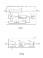
- FIG. 1 is a schematic block diagram of a power transforming apparatus according to a preferred embodiment of the present invention
- FIG. 2 is a schematic block diagram of a slope compensation unit according to the present invention.
- FIG. 3 is a schematic diagram of an actual current waveform of the energy transformation signal according to the present invention.
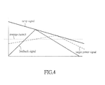
- FIG. 4 is a schematic diagram of the signals according to the present invention.
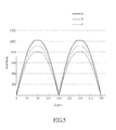
- FIG. 5 is a schematic diagram of the target power signal according to the present invention.
- FIG. 6 is a schematic block diagram of a power transforming apparatus according to another preferred embodiment of the present invention.
- FIG. 1 is a schematic block diagram of a power transforming apparatus according to a preferred embodiment of the present invention.
- the power transforming apparatus 1 transforms an energy signal S IN into an energy transformation signal S OUT and outputs the energy transformation signal S OUT .
- the energy signal S IN can be a direct current (DC) voltage signal
- the power transforming apparatus 1 transforms the DC voltage signal into an alternating current (AC) voltage signal (i.e. DC to AC) to output the energy transformation signal S OUT .
- the energy signal S IN can be a DC voltage signal
- the power transforming apparatus 1 transforms the DC voltage signal into a DC voltage signal (i.e. DC to DC) to output the energy transformation signal S OUT .
- the outputted energy transformation signal S OUT can meet the requirement of the load (not shown).
- the power transforming apparatus 1 transforms the DC voltage signal into the AC voltage signal.
- the power transforming apparatus 1 can implements a full wave rectification to the energy signal S IN .
- the power transforming apparatus 1 includes a control unit 11, a pulse width modulation (PWM) unit 12, a transformation unit 13, a slope compensation unit 14 and a feedback unit 15.
- PWM pulse width modulation
- the control unit 11 can be a micro control unit (MCU) for example to output a target power signal S TP , which can be a computer instruction.
- the control unit 11 can obtain the voltage or current value of the energy signal S IN inputted to the power transforming apparatus 1 and a feedback signal S FB to output the target power signal S TP .
- the feedback signal S FB can be the voltage or current value of the energy transformation signal S OUT outputted by the power transforming apparatus 1.
- the target power signal S TP is generated according to the voltage value of the energy signal S IN inputted to the power transforming apparatus 1
- the feedback signal S FB is the current value of the energy transformation signal S OUT outputted by the power transforming apparatus 1.
- this invention is not limited thereto.
- the target power signal S TP is used to determine the peak of the output of the transformation unit 13, which can be corresponding to a target current value of the energy signal S IN after the transformation or can be higher than the actual current value obtained after the transformation.
- the PWM unit 12 is coupled with the control unit 11, and can generate a switch signal S S .
- the switch signal SS can be a pulse width modulation (PWM) signal.
- the transformation unit 13 is coupled with the PWM unit 12, and can transform the energy signal S IN into the energy transformation signal S OUT .
- the transformation unit 13 transforms the energy signal S IN into the energy transformation signal S OUT according to the switch signal S S .
- the transformation unit 13 can be a DC to AC transformation unit or a DC to DC transformation unit according to the type of the load.
- the transformation unit 13 is a DC to AC transformation unit for example.
- the feedback unit 15 can be a current sensor (e.g. an inductive element) to sense the current value of the energy transformation signal S OUT that is outputted by the power transforming apparatus 1 to generate the feedback signal S FB .
- the slope compensation unit 14 is coupled with the control unit 11 and the PWM unit 12, and can implement a slope compensation according to the target power signal S TP and the feedback signal S FB to output a compensation signal S COMP to the PWM unit 12. Then, the PWM unit 12 generates the switch signal S S according to the target power signal S TP and the compensation signal S COMP .
- the power transforming apparatus 1 operates in a current mode.
- the current feedback signal is usually generated from the inductor current, and thus the generated peak inductor current will be processed directly by the control system of the error signal. Therefore, the failure due to the overhigh current can be prevented.
- the current mode can control and adjust the inductor current, the inductor pole or the delay in the control loop of the whole system can be effectively eliminated, and thereby the transient response of the system is improved.
- the current mode control provides many functions, such as the protection of the peak current of the transistor, elimination of the ratcheting of the magnetic field of the magnetic element, restraint of the change of the input voltage, and convenient control loop compensation.
- the maximum inductor current is controlled by the error voltage, and thereby the inductor becomes the voltage-controlled current source.
- the inductor will not generate poles in the frequency response of the control loop, which makes the loop become more stable from the unpredicted unstable situation, so that the loop filter can be designed more easily.
- the target power signal S TP is a current instruction emitted by the control unit 11 to implement a full wave rectification to the energy signal S IN and determine the peak current of the output of the transformation unit 13, which is higher than the current value of the energy transformation signal S OUT .
- the PWM unit 12 controls the maximum duty cycle of the switch signal S S according to the target power signal S TP .
- the switch signal S S may not have the maximum duty cycle. In other words, the duty cycle of the switch signal S S will be adjusted downward because of the compensation signal S COMP .
- the average current outputted by the transformation unit 13 is over half the peak current and higher than the value that is calculated by the measured peak current.
- the output voltage of the transformation unit 13 will be over the required value and climb continuously. Besides, the output voltage can not be reduced as below the required level until the slowly-reacted voltage control loop readjusts the current-set point.
- the above-mentioned process is called second harmonic generation, and will repeat again and again.
- the slope compensation technology is presented herein. Because the compensation signal S COMP is generated through the slope compensation, the energy transformation signal S OUT outputted by the transformation unit 13 can be controlled at the desired current, and the whole system can leave out the PID computation and eliminate the drawback of the second harmonic generation. Besides, the current stability and anti-noise capability can be enhanced. Furthermore, since the system just needs the voltage loop computation and doesn't need the current loop PID computation, the requirement of computing capability of the control unit 11 can be reduced a lot.
- FIG. 2 is a schematic block diagram of a slope compensation unit according to the present invention.
- the slope compensation unit 14 can include a slop generator 141, a digital to analog converter 142 and a comparator 143.
- the control unit 11 further outputs a descending tendency signal S DT to the slope compensation unit 14.
- the descending tendency signal S DT can be a computer instruction.
- the slope compensation unit 14 processes the target power signal S TP according to the descending tendency signal S DT to generate a ramp signal S RAMP .
- the slope generator 141 receives the target power signal S TP and the descending tendency signal S DT , and, according to them, outputs the ramp signal S RAMP to the digital to analog converter 142.
- the digital to analog converter 142 is coupled with the slope generator 141 and receives the ramp signal S RAMP , and converts the ramp signal S RAMP (digital signal) into an analog signal.
- the comparator 143 is coupled with the digital to analog converter 142 and the PWM unit 12. The comparator 143 receives the ramp signal S RAMP and the feedback signal S FB , and outputs the compensation signal S COMP according to the ramp signal S RAMP and the feedback signal S FB .
- FIG. 3 is a schematic diagram of an actual current waveform of the energy transformation signal according to the present invention. As shown in FIG. 3 , the current waveform of the energy transformation signal S OUT is not a smooth sine wave like its envelope, but is jagged.
- FIG. 4 is a schematic diagram of the signals according to the present invention.
- the ramp signal S RAMP is a progressively decreasing signal with a negative slope, and the slop is determined by the descending tendency signal S DT .
- the ramp signal S RAMP must pass through the peak point of the target power signal S TP (current instruction). Thereby, the ramp signal S RAMP can be generated according to the descending tendency signal S DT and the target power signal S TP (current instruction).
- the ramp signal S RAMP denotes the allowed maximum current value of the feedback signal S FB at different times in a PWM period.
- the comparator 143 will change the level of the compensation signal S COMP , so that the PWM unit 12 doesn't drive the transformation unit 13 to output more current anymore. Thereby, the current of the energy transformation signal S OUT will be reduced, and accordingly the current of the feedback signal S FB is reduced. In other words, the slope compensation effect provided by the slope compensation unit 14 is decreased as time goes by. So, not only the magnitude of the target power signal S TP (current instruction) but also the compensation signal S COMP determines the duty cycle of the switch signal S S .
- the slope compensation is implemented to the value given to the transformation unit 13 with a decrement of a slope compensation value in a fixed period of time, and therefore the second harmonic generation can be prevented, and thus the current waveform of the energy transformation signal S OUT can more approximate a smooth sine wave.
- the ratio of the slope compensation is raised herein. Practically, raising the ratio of the slope compensation can effectively enhance the current stability.
- the ratio of the slope compensation is adjusted according to the magnitude of the current instruction so that the current stability and anti-noise capability both can be enhanced.
- FIG. 5 is a schematic diagram of the target power signal according to the present invention, and shows the influence of the slope compensation on the target power signal.
- subtracting the slope compensation value from the target power signal can obtain the influence magnitude of the slope compensation on the target power signal.
- subtracting the slope compensation value from the maximum value a of the target power signal computed by the control unit 11 can obtain the maximum influence magnitude of the slope compensation on the target power signal, i.e. the minimum value b of the target power signal.
- subtracting half the maximum influence magnitude of the slope compensation on the target power signal from half the maximum value of the target power signal can obtain the middle value c of the target power signal.
- FIG. 6 is a schematic block diagram of a power transforming apparatus 1a according to an embodiment of the present invention.
- the power transforming apparatus 1a is similar to the power transforming apparatus 1, but the transformation unit 13a is further illustrated in this embodiment.
- the transformation unit 13a includes a voltage sensor 131, a transformation circuit 132 and a driving circuit 133.
- the voltage sensor 131 is coupled with the control unit 11 and the transformation circuit 132.
- the voltage sensor 131 can receive the energy signal S IN and detect the voltage value of the energy signal S IN to provide the basis for the control unit 11 for generating the target power signal S TP .
- the transformation circuit 132 is coupled with the voltage sensor 131, the driving circuit 133 and the feedback unit 15.
- the transformation circuit 132 includes a plurality of insulated gate bipolar transistors (IGBT) or metal-oxide-semiconductor field-effect transistors (MOSFET), and can transform the energy signal S IN into the energy transformation signal S OUT .
- IGBT insulated gate bipolar transistors
- MOSFET metal-oxide-semiconductor field-effect transistors
- the driving circuit 133 is coupled with the PWM unit 12 and the transformation circuit 132.
- the driving circuit 133 can, according to the switch signal S S outputted by the PWM unit 12, drive the transformation circuit 132 to operate for transforming the energy signal S IN into the energy transformation signal S OUT .
- the power transforming apparatus uses the digital dynamic slope compensation mechanism to eliminate the problem of second harmonic generation. Therefore, the stability of the outputted energy transformation signal is enhanced and the noise influence is reduced. Besides, by using the outputted current as the feedback, the failure of the power transforming apparatus due to the overhigh current can be prevented, and thus the reliability is increased.
Abstract
Description
- The present invention relates to a power transforming apparatus.
- With the rising cost of energy, the raised environmental consciousness and the energy regulations made by countries, the standard of energy transformation efficiency of electronic products seems more and more strict. Thus, a conventional power transforming apparatus, such as a power supply, gradually shows its lack of achieving such standard. Therefore, the switched-mode power supply (SMPS) with better energy transformation efficiency becomes more promising in the market.
- The SMPS is mainly divided into an analog control type and a digital control type. Because the analog control type easily generates clipping and thus results in the worse energy transformation efficiency, it is gradually replaced by the digital control type. The digital control type can overcome the drawback of the analog control type by using the proportional integral derivative controller (PID controller). However, the PID controller is short of the slope compensation mechanism, and therefore, if the feedback system is affected by noise signals to generate unexpected computing result of the PID controller, the output oscillation will occur. Besides, the PID controller needs to execute a great deal of computation so it needs to be configured with a micro control unit (MCU) with higher processing efficiency, and therefore the total cost will be increased.
- Therefore, it is an important subject to provide a power transforming apparatus that is not only capable of slope compensation mechanism but has less computation so that the cost can be reduced.
- In view of the foregoing subject, an objective of this present invention is to provide a power transforming apparatus that is not only capable of slope compensation mechanism but has less computation so as to reduce cost.
- To achieve the above objective, a power transforming apparatus according to the present invention implements a transformation of an energy signal and includes a control unit, a pulse width modulation (PWM) unit, a transformation unit, and a slope compensation unit. The control unit outputs a target power signal. The PWM unit is coupled with the control unit and generates a switch signal. The transformation unit is coupled with the PWM unit, and implements a power transforming of the energy signal to output an energy transformation signal according to the switch signal. The slope compensation unit is coupled with the control unit and the PWM unit, and implements a slope compensation, according to the target power signal and a feedback signal, to output a compensation signal to the PWM unit. The switch signal is generated according to the target power signal and the compensation signal.
- In one embodiment, the control unit outputs a descending tendency signal to the slope compensation unit. The slope compensation unit processes the target power signal to generate a ramp signal according to the descending tendency signal, and outputs the compensation signal according to the ramp signal and the feedback signal.
- In one embodiment, each of the target power signal and the descending tendency signal is a computer instruction.
- In one embodiment, the slope compensation unit includes a slope generator, a digital to analog converter and a comparator. The slope generator outputs the ramp signal according to the target power signal and the descending tendency signal. The digital to analog converter is coupled with the slope generator, and converts the ramp signal of digital signal into an analog signal. The comparator is coupled with the digital to analog converter and the PWM unit, and outputs the compensation signal according to the ramp signal and the feedback signal.
- In one embodiment, a representative value of the target power signal is more than a required value of an actual transformation.
- In one embodiment, the energy signal is processed with a full wave rectification.
- In one embodiment, the control unit generates the target power signal according to the voltage of the energy signal and the feedback signal.
- In one embodiment, the transformation unit is a DC to AC transformation unit or a DC to DC transformation unit.
- In one embodiment, the target power signal is corresponding to a target current value of the energy signal after the transformation.
- In one embodiment, the power transforming apparatus further includes a feedback unit, which generates the feedback signal according to the energy transformation signal.
- As mentioned above, the power transforming apparatus according to the present invention uses the digital dynamic slope compensation mechanism to eliminate the problem of second harmonic generation. Therefore, the stability of the outputted energy transformation signal is enhanced and the noise influence is reduced. Besides, by using the outputted current as the feedback, the failure of the power transforming apparatus due to the overhigh current can be prevented, and thus the reliability is increased.
- The present invention will become more fully understood from the detailed description and accompanying drawings, which are given for illustration only, and thus are not limitative of the present invention, and wherein:
-
FIG. 1 is a schematic block diagram of a power transforming apparatus according to a preferred embodiment of the present invention; -
FIG. 2 is a schematic block diagram of a slope compensation unit according to the present invention; -
FIG. 3 is a schematic diagram of an actual current waveform of the energy transformation signal according to the present invention; -
FIG. 4 is a schematic diagram of the signals according to the present invention; -
FIG. 5 is a schematic diagram of the target power signal according to the present invention; and -
FIG. 6 is a schematic block diagram of a power transforming apparatus according to another preferred embodiment of the present invention. - The present invention will be apparent from the following detailed description, which proceeds with reference to the accompanying drawings, wherein the same references relate to the same elements.
-
FIG. 1 is a schematic block diagram of a power transforming apparatus according to a preferred embodiment of the present invention. As shown inFIG. 1 , the power transforming apparatus 1 transforms an energy signal SIN into an energy transformation signal SOUT and outputs the energy transformation signal SOUT. For example, the energy signal SIN can be a direct current (DC) voltage signal, and the power transforming apparatus 1 transforms the DC voltage signal into an alternating current (AC) voltage signal (i.e. DC to AC) to output the energy transformation signal SOUT. Otherwise, the energy signal SIN can be a DC voltage signal, and the power transforming apparatus 1 transforms the DC voltage signal into a DC voltage signal (i.e. DC to DC) to output the energy transformation signal SOUT. Thereby, the outputted energy transformation signal SOUT can meet the requirement of the load (not shown). Herein as an example, the power transforming apparatus 1 transforms the DC voltage signal into the AC voltage signal. Besides, the power transforming apparatus 1 can implements a full wave rectification to the energy signal SIN. - The power transforming apparatus 1 includes a
control unit 11, a pulse width modulation (PWM)unit 12, atransformation unit 13, aslope compensation unit 14 and afeedback unit 15. - As an embodiment, the
control unit 11 can be a micro control unit (MCU) for example to output a target power signal STP, which can be a computer instruction. Practically, thecontrol unit 11 can obtain the voltage or current value of the energy signal SIN inputted to the power transforming apparatus 1 and a feedback signal SFB to output the target power signal STP. The feedback signal SFB can be the voltage or current value of the energy transformation signal SOUT outputted by the power transforming apparatus 1. In this embodiment, for example, the target power signal STP is generated according to the voltage value of the energy signal SIN inputted to the power transforming apparatus 1, and the feedback signal SFB is the current value of the energy transformation signal SOUT outputted by the power transforming apparatus 1. However, this invention is not limited thereto. - The target power signal STP is used to determine the peak of the output of the
transformation unit 13, which can be corresponding to a target current value of the energy signal SIN after the transformation or can be higher than the actual current value obtained after the transformation. ThePWM unit 12 is coupled with thecontrol unit 11, and can generate a switch signal SS. In this embodiment, the switch signal SS can be a pulse width modulation (PWM) signal. Thetransformation unit 13 is coupled with thePWM unit 12, and can transform the energy signal SIN into the energy transformation signal SOUT. In detail, thetransformation unit 13 transforms the energy signal SIN into the energy transformation signal SOUT according to the switch signal SS. Practically, thetransformation unit 13 can be a DC to AC transformation unit or a DC to DC transformation unit according to the type of the load. Herein, thetransformation unit 13 is a DC to AC transformation unit for example. - The
feedback unit 15 can be a current sensor (e.g. an inductive element) to sense the current value of the energy transformation signal SOUT that is outputted by the power transforming apparatus 1 to generate the feedback signal SFB. When thefeedback unit 15 is a current sensor, the system failure of the power transforming apparatus 1 because of the overhigh current can be prevented. Theslope compensation unit 14 is coupled with thecontrol unit 11 and thePWM unit 12, and can implement a slope compensation according to the target power signal STP and the feedback signal SFB to output a compensation signal SCOMP to thePWM unit 12. Then, thePWM unit 12 generates the switch signal SS according to the target power signal STP and the compensation signal SCOMP. - For example, the power transforming apparatus 1 operates in a current mode. In the current mode control system, the current feedback signal is usually generated from the inductor current, and thus the generated peak inductor current will be processed directly by the control system of the error signal. Therefore, the failure due to the overhigh current can be prevented. Besides, because the current mode can control and adjust the inductor current, the inductor pole or the delay in the control loop of the whole system can be effectively eliminated, and thereby the transient response of the system is improved.
- The current mode control provides many functions, such as the protection of the peak current of the transistor, elimination of the ratcheting of the magnetic field of the magnetic element, restraint of the change of the input voltage, and convenient control loop compensation. In other words, the maximum inductor current is controlled by the error voltage, and thereby the inductor becomes the voltage-controlled current source. As the current source, the inductor will not generate poles in the frequency response of the control loop, which makes the loop become more stable from the unpredicted unstable situation, so that the loop filter can be designed more easily.
- The target power signal STP is a current instruction emitted by the
control unit 11 to implement a full wave rectification to the energy signal SIN and determine the peak current of the output of thetransformation unit 13, which is higher than the current value of the energy transformation signal SOUT. ThePWM unit 12 controls the maximum duty cycle of the switch signal SS according to the target power signal STP. However, because the duty cycle of the switch signal SS is also affected by the feedback compensation signal SCOMP, the switch signal SS may not have the maximum duty cycle. In other words, the duty cycle of the switch signal SS will be adjusted downward because of the compensation signal SCOMP. - When the duty cycle of the switch signal SS is over 50%, the average current outputted by the
transformation unit 13 is over half the peak current and higher than the value that is calculated by the measured peak current. In this situation, if there is no operation of theslope compensation unit 14, the output voltage of thetransformation unit 13 will be over the required value and climb continuously. Besides, the output voltage can not be reduced as below the required level until the slowly-reacted voltage control loop readjusts the current-set point. The above-mentioned process is called second harmonic generation, and will repeat again and again. - In order to solve the stability problem of the current mode control, the slope compensation technology is presented herein. Because the compensation signal SCOMP is generated through the slope compensation, the energy transformation signal SOUT outputted by the
transformation unit 13 can be controlled at the desired current, and the whole system can leave out the PID computation and eliminate the drawback of the second harmonic generation. Besides, the current stability and anti-noise capability can be enhanced. Furthermore, since the system just needs the voltage loop computation and doesn't need the current loop PID computation, the requirement of computing capability of thecontrol unit 11 can be reduced a lot. -
FIG. 2 is a schematic block diagram of a slope compensation unit according to the present invention. As shown inFIG. 2 , theslope compensation unit 14 can include aslop generator 141, a digital toanalog converter 142 and acomparator 143. - The
control unit 11 further outputs a descending tendency signal SDT to theslope compensation unit 14. The descending tendency signal SDT can be a computer instruction. Theslope compensation unit 14 processes the target power signal STP according to the descending tendency signal SDT to generate a ramp signal SRAMP. In detail, theslope generator 141 receives the target power signal STP and the descending tendency signal SDT, and, according to them, outputs the ramp signal SRAMP to the digital toanalog converter 142. - The digital to
analog converter 142 is coupled with theslope generator 141 and receives the ramp signal SRAMP, and converts the ramp signal SRAMP (digital signal) into an analog signal. Thecomparator 143 is coupled with the digital toanalog converter 142 and thePWM unit 12. Thecomparator 143 receives the ramp signal SRAMP and the feedback signal SFB, and outputs the compensation signal SCOMP according to the ramp signal SRAMP and the feedback signal SFB. -
FIG. 3 is a schematic diagram of an actual current waveform of the energy transformation signal according to the present invention. As shown inFIG. 3 , the current waveform of the energy transformation signal SOUT is not a smooth sine wave like its envelope, but is jagged. -
FIG. 4 is a schematic diagram of the signals according to the present invention. As shown inFIG. 4 , during a PWM period, the ramp signal SRAMP is a progressively decreasing signal with a negative slope, and the slop is determined by the descending tendency signal SDT. Besides, the ramp signal SRAMP must pass through the peak point of the target power signal STP (current instruction). Thereby, the ramp signal SRAMP can be generated according to the descending tendency signal SDT and the target power signal STP (current instruction). The ramp signal SRAMP denotes the allowed maximum current value of the feedback signal SFB at different times in a PWM period. Besides, when the current value of the feedback signal SFB reaches the allowed maximum current value at a certain time, thecomparator 143 will change the level of the compensation signal SCOMP, so that thePWM unit 12 doesn't drive thetransformation unit 13 to output more current anymore. Thereby, the current of the energy transformation signal SOUT will be reduced, and accordingly the current of the feedback signal SFB is reduced. In other words, the slope compensation effect provided by theslope compensation unit 14 is decreased as time goes by. So, not only the magnitude of the target power signal STP (current instruction) but also the compensation signal SCOMP determines the duty cycle of the switch signal SS. Therefore, according to the duty cycle of the PWM and the system frequency, the slope compensation is implemented to the value given to thetransformation unit 13 with a decrement of a slope compensation value in a fixed period of time, and therefore the second harmonic generation can be prevented, and thus the current waveform of the energy transformation signal SOUT can more approximate a smooth sine wave. - In sum, when the outputted current is higher and higher, the generated noise is larger and larger. For such positive correlation, the ratio of the slope compensation is raised herein. Practically, raising the ratio of the slope compensation can effectively enhance the current stability. In the present invention, the ratio of the slope compensation is adjusted according to the magnitude of the current instruction so that the current stability and anti-noise capability both can be enhanced.
-
FIG. 5 is a schematic diagram of the target power signal according to the present invention, and shows the influence of the slope compensation on the target power signal. As shown inFIG. 5 , subtracting the slope compensation value from the target power signal can obtain the influence magnitude of the slope compensation on the target power signal. For example, subtracting the slope compensation value from the maximum value a of the target power signal computed by thecontrol unit 11 can obtain the maximum influence magnitude of the slope compensation on the target power signal, i.e. the minimum value b of the target power signal. Besides, subtracting half the maximum influence magnitude of the slope compensation on the target power signal from half the maximum value of the target power signal can obtain the middle value c of the target power signal. -
FIG. 6 is a schematic block diagram of a power transforming apparatus 1a according to an embodiment of the present invention. The power transforming apparatus 1a is similar to the power transforming apparatus 1, but thetransformation unit 13a is further illustrated in this embodiment. Thetransformation unit 13a includes avoltage sensor 131, atransformation circuit 132 and adriving circuit 133. - The
voltage sensor 131 is coupled with thecontrol unit 11 and thetransformation circuit 132. Thevoltage sensor 131 can receive the energy signal SIN and detect the voltage value of the energy signal SIN to provide the basis for thecontrol unit 11 for generating the target power signal STP. - The
transformation circuit 132 is coupled with thevoltage sensor 131, the drivingcircuit 133 and thefeedback unit 15. Thetransformation circuit 132 includes a plurality of insulated gate bipolar transistors (IGBT) or metal-oxide-semiconductor field-effect transistors (MOSFET), and can transform the energy signal SIN into the energy transformation signal SOUT. - The driving
circuit 133 is coupled with thePWM unit 12 and thetransformation circuit 132. The drivingcircuit 133 can, according to the switch signal SS outputted by thePWM unit 12, drive thetransformation circuit 132 to operate for transforming the energy signal SIN into the energy transformation signal SOUT. - In summary, the power transforming apparatus according to the present invention uses the digital dynamic slope compensation mechanism to eliminate the problem of second harmonic generation. Therefore, the stability of the outputted energy transformation signal is enhanced and the noise influence is reduced. Besides, by using the outputted current as the feedback, the failure of the power transforming apparatus due to the overhigh current can be prevented, and thus the reliability is increased.
- Although the present invention has been described with reference to specific embodiments, this description is not meant to be construed in a limiting sense. Various modifications of the disclosed embodiments, as well as alternative embodiments, will be apparent to persons skilled in the art. It is, therefore, contemplated that the appended claims will cover all modifications that fall within the true scope of the invention.
Claims (19)
- A power transforming apparatus implementing a transformation of an energy signal, the power transforming apparatus comprising:a control unit outputting a target power signal;a pulse width modulation (PWM) unit coupled with the control unit and generating a switch signal;a transformation unit coupled with the PWM unit, and implementing a power transforming of the energy signal to output an energy transformation signal according to the switch signal; anda slope compensation unit coupled with the control unit and the PWM unit, and implementing a slope compensation, according to the target power signal and a feedback signal, to output a compensation signal to the PWM unit, wherein the switch signal is generated according to the target power signal and the compensation signal.
- The power transforming apparatus as recited in claim 1, wherein the control unit outputs a descending tendency signal to the slope compensation unit, and the slope compensation unit processes the target power signal to generate a ramp signal according to the descending tendency signal, and outputs the compensation signal according to the ramp signal and the feedback signal.
- The power transforming apparatus as recited in claim 2, wherein each of the target power signal and the descending tendency signal is a computer instruction.
- The power transforming apparatus as recited in claim 2, wherein the slope compensation unit comprises:a slope generator outputting the ramp signal according to the target power signal and the descending tendency signal;a digital to analog converter coupled with the slope generator and converting the ramp signal of digital signal into an analog signal; anda comparator coupled with the digital to analog converter and the PWM unit, and outputting the compensation signal according to the ramp signal and the feedback signal.
- The power transforming apparatus as recited in claim 4, wherein the ramp signal denotes the allowed maximum current value of the feedback signal at different times in a PWM period, when the current value of the feedback signal reaches the allowed maximum current value at a certain time, the comparator changes the level of the compensation signal, so that the PWM unit doesn't drive the transformation unit to output current.
- The power transforming apparatus as recited in claim 1, wherein a representative value of the target power signal is more than a required value of an actual transformation.
- The power transforming apparatus as recited in claim 1, wherein the energy signal is processed with a full wave rectification.
- The power transforming apparatus as recited in claim 1, wherein the control unit generates the target power signal according to the voltage of the energy signal and the feedback signal.
- The power transforming apparatus as recited in claim 1, wherein the transformation unit is a DC to AC transformation unit or a DC to DC transformation unit
- The power transforming apparatus as recited in claim 1, wherein the target power signal is corresponding to a target current value of the energy signal after the transformation.
- The power transforming apparatus as recited in claim 1, further comprising:a feedback unit generating the feedback signal according to the energy transformation signal.
- The power transforming apparatus as recited in claim 11, wherein the feedback unit is a current sensor to sense the current value of the energy transformation signal outputted by the power transforming apparatus to generate the feedback signal.
- The power transforming apparatus as recited in claim 11, wherein the feedback signal is a voltage or current value of the energy transformation signal outputted by the power transforming apparatus.
- The power transforming apparatus as recited in claim 1, wherein the control unit is a micro control unit (MCU).
- The power transforming apparatus as recited in claim 1, wherein the switch signal is a pulse width modulation (PWM) signal.
- The power transforming apparatus as recited in claim 15, wherein the PWM unit controls the maximum duty cycle of the switch signal according to the target power signal.
- The power transforming apparatus as recited in claim 1, further comprising:a voltage sensor coupled with the control unit, receiving the energy signal and detecting the voltage value of the energy signal to provide the basis for the control unit for generating the target power signal;a transformation circuit coupled with the voltage sensor and the feedback unit and transforming the energy signal into the energy transformation signal; anda driving circuit coupled with the PWM unit and the transformation circuit and driving the transformation circuit according to the switch signal outputted by the PWM unit to operate for transforming the energy signal into the energy transformation signal.
- The power transforming apparatus as recited in claim 17, wherein the transformation circuit includes a plurality of insulated gate bipolar transistors (IGBT) or metal-oxide-semiconductor field-effect transistors (MOSFET).
- The power transforming apparatus as recited in claim 1, which operates in a current mode.
Applications Claiming Priority (1)
| Application Number | Priority Date | Filing Date | Title |
|---|---|---|---|
| CN201310134082.4A CN104113193B (en) | 2013-04-17 | 2013-04-17 | Power conversion device |
Publications (2)
| Publication Number | Publication Date |
|---|---|
| EP2793382A2 true EP2793382A2 (en) | 2014-10-22 |
| EP2793382A3 EP2793382A3 (en) | 2014-11-19 |
Family
ID=48986023
Family Applications (1)
| Application Number | Title | Priority Date | Filing Date |
|---|---|---|---|
| EP20130180751 Ceased EP2793382A3 (en) | 2013-04-17 | 2013-08-16 | Power transforming apparatus |
Country Status (3)
| Country | Link |
|---|---|
| US (1) | US9130474B2 (en) |
| EP (1) | EP2793382A3 (en) |
| CN (1) | CN104113193B (en) |
Families Citing this family (7)
| Publication number | Priority date | Publication date | Assignee | Title |
|---|---|---|---|---|
| US9748781B2 (en) * | 2014-06-24 | 2017-08-29 | Intersil Americas LLC | Voltage converters and methods for use therewith |
| US20160052145A1 (en) * | 2014-08-19 | 2016-02-25 | GM Global Technology Operations LLC | Conformable holding device |
| TWI542114B (en) * | 2015-06-17 | 2016-07-11 | 台達電子工業股份有限公司 | Photovoltaic inverter grid-connected system and method for implementing three-phase ac grid-connected transition |
| US10720835B2 (en) | 2017-09-18 | 2020-07-21 | Cirrus Logic, Inc. | Limiting average current in a peak-controlled boost converter |
| US11031867B2 (en) * | 2017-12-08 | 2021-06-08 | Cirrus Logic, Inc. | Digital-to-analog converter with embedded minimal error adaptive slope compensation for digital peak current controlled switched mode power supply |
| US10734885B2 (en) | 2018-06-19 | 2020-08-04 | Cirrus Logic, Inc. | Removal of near DC errors in a peak-controlled boost converter using a low-bandwidth secondary control loop |
| CN115089839B (en) * | 2022-08-25 | 2022-11-11 | 柏斯速眠科技(深圳)有限公司 | Head detection method and system and control method and system of sleep-assisting device |
Family Cites Families (10)
| Publication number | Priority date | Publication date | Assignee | Title |
|---|---|---|---|---|
| US5525874A (en) | 1995-01-30 | 1996-06-11 | Delco Electronics Corp. | Digital slope compensation in a current controller |
| CN100413190C (en) * | 2005-03-11 | 2008-08-20 | 昂宝电子(上海)有限公司 | System and method for controlling frequency of adaptive switch |
| DE102007028568B4 (en) * | 2006-06-23 | 2009-12-03 | Mediatek Inc. | switching regulators |
| US8138734B2 (en) * | 2009-04-06 | 2012-03-20 | Monolithic Power Systems, Inc. | Accurate current limit for peak current mode DC-DC converter |
| EP2299577B1 (en) | 2009-09-18 | 2012-08-01 | DET International Holding Limited | Digital slope compensation for current mode control |
| JP5464695B2 (en) * | 2009-11-05 | 2014-04-09 | ルネサスエレクトロニクス株式会社 | DC-DC converter, DC voltage conversion method |
| CN102035384B (en) * | 2010-12-13 | 2014-12-24 | 成都芯源系统有限公司 | Switching converter circuit and power conversion method |
| US8773097B2 (en) | 2011-01-06 | 2014-07-08 | Texas Instruments Incorporated | Digital peak current mode control for switch-mode power converters |
| US8934266B2 (en) * | 2011-08-26 | 2015-01-13 | System General Corp. | Adaptive slope compensation programmable by input voltage of power converter |
| TW201351861A (en) * | 2012-06-08 | 2013-12-16 | Novatek Microelectronics Corp | Method of controlling a power converting device and related circuit |
-
2013
- 2013-04-17 CN CN201310134082.4A patent/CN104113193B/en not_active Expired - Fee Related
- 2013-08-15 US US13/967,783 patent/US9130474B2/en not_active Expired - Fee Related
- 2013-08-16 EP EP20130180751 patent/EP2793382A3/en not_active Ceased
Non-Patent Citations (1)
| Title |
|---|
| None |
Also Published As
| Publication number | Publication date |
|---|---|
| US20140313799A1 (en) | 2014-10-23 |
| EP2793382A3 (en) | 2014-11-19 |
| CN104113193B (en) | 2017-10-03 |
| US9130474B2 (en) | 2015-09-08 |
| CN104113193A (en) | 2014-10-22 |
Similar Documents
| Publication | Publication Date | Title |
|---|---|---|
| US9130474B2 (en) | Power transforming apparatus with digital control unit | |
| EP2919374B1 (en) | Duty-ratio controller | |
| JP6158739B2 (en) | Power converter | |
| US9318976B1 (en) | Adjustable PWM method to increase low speed starting torque and inverter voltage measurement accuracy | |
| EP2528221A2 (en) | Multi-phase active rectifier | |
| JP6479160B2 (en) | Converter device | |
| US10199946B2 (en) | Systems and methods for adjusting peak frequencies with duty cycles | |
| US10170984B2 (en) | Switched mode power converter with peak current control | |
| EP2770622A2 (en) | Control device, control method, and power supply device | |
| KR20200040673A (en) | Switched mode power supply with pfc burst mode control | |
| JP2012205331A (en) | Power supply device | |
| CN114337230A (en) | Slow starting method of switching regulator | |
| JP6405906B2 (en) | AC-DC converter controller | |
| JP6070715B2 (en) | Power converter | |
| US10530255B2 (en) | Peak current control for a power switch of a power converter | |
| JP5323383B2 (en) | Power converter | |
| US20220255415A1 (en) | Control circuit for power converter apparatus provided with pfc circuit operating in current-critical mode | |
| CN114094851A (en) | Power conversion device | |
| JP2006353048A (en) | Power supply | |
| JP6286380B2 (en) | Power converter | |
| JPWO2019234846A1 (en) | Power converter | |
| CN110299823B (en) | Apparatus and method for controlling power supply | |
| WO2021028972A1 (en) | Control circuit for power conversion device | |
| JP4966252B2 (en) | Switching power supply | |
| JP2016220342A (en) | Switching power supply device |
Legal Events
| Date | Code | Title | Description |
|---|---|---|---|
| PUAL | Search report despatched |
Free format text: ORIGINAL CODE: 0009013 |
|
| PUAI | Public reference made under article 153(3) epc to a published international application that has entered the european phase |
Free format text: ORIGINAL CODE: 0009012 |
|
| 17P | Request for examination filed |
Effective date: 20130816 |
|
| AK | Designated contracting states |
Kind code of ref document: A2 Designated state(s): AL AT BE BG CH CY CZ DE DK EE ES FI FR GB GR HR HU IE IS IT LI LT LU LV MC MK MT NL NO PL PT RO RS SE SI SK SM TR |
|
| AX | Request for extension of the european patent |
Extension state: BA ME |
|
| AK | Designated contracting states |
Kind code of ref document: A3 Designated state(s): AL AT BE BG CH CY CZ DE DK EE ES FI FR GB GR HR HU IE IS IT LI LT LU LV MC MK MT NL NO PL PT RO RS SE SI SK SM TR |
|
| AX | Request for extension of the european patent |
Extension state: BA ME |
|
| RIC1 | Information provided on ipc code assigned before grant |
Ipc: H02M 3/00 20060101ALI20141014BHEP Ipc: H02M 1/00 20070101ALI20141014BHEP Ipc: H02M 7/537 20060101AFI20141014BHEP |
|
| R17P | Request for examination filed (corrected) |
Effective date: 20150430 |
|
| RBV | Designated contracting states (corrected) |
Designated state(s): AL AT BE BG CH CY CZ DE DK EE ES FI FR GB GR HR HU IE IS IT LI LT LU LV MC MK MT NL NO PL PT RO RS SE SI SK SM TR |
|
| 17Q | First examination report despatched |
Effective date: 20170220 |
|
| STAA | Information on the status of an ep patent application or granted ep patent |
Free format text: STATUS: THE APPLICATION HAS BEEN REFUSED |
|
| 18R | Application refused |
Effective date: 20181029 |