EP2930470A1 - Electrical activity sensor device for detecting electrical activity and electrical activity monitoring apparatus - Google Patents
Electrical activity sensor device for detecting electrical activity and electrical activity monitoring apparatus Download PDFInfo
- Publication number
- EP2930470A1 EP2930470A1 EP14305542.4A EP14305542A EP2930470A1 EP 2930470 A1 EP2930470 A1 EP 2930470A1 EP 14305542 A EP14305542 A EP 14305542A EP 2930470 A1 EP2930470 A1 EP 2930470A1
- Authority
- EP
- European Patent Office
- Prior art keywords
- electrical
- rfid
- antenna
- electrical activity
- dipole
- Prior art date
- Legal status (The legal status is an assumption and is not a legal conclusion. Google has not performed a legal analysis and makes no representation as to the accuracy of the status listed.)
- Granted
Links
Images


Classifications
-
- G—PHYSICS
- G06—COMPUTING; CALCULATING OR COUNTING
- G06K—GRAPHICAL DATA READING; PRESENTATION OF DATA; RECORD CARRIERS; HANDLING RECORD CARRIERS
- G06K7/00—Methods or arrangements for sensing record carriers, e.g. for reading patterns
- G06K7/10—Methods or arrangements for sensing record carriers, e.g. for reading patterns by electromagnetic radiation, e.g. optical sensing; by corpuscular radiation
- G06K7/10009—Methods or arrangements for sensing record carriers, e.g. for reading patterns by electromagnetic radiation, e.g. optical sensing; by corpuscular radiation sensing by radiation using wavelengths larger than 0.1 mm, e.g. radio-waves or microwaves
- G06K7/10316—Methods or arrangements for sensing record carriers, e.g. for reading patterns by electromagnetic radiation, e.g. optical sensing; by corpuscular radiation sensing by radiation using wavelengths larger than 0.1 mm, e.g. radio-waves or microwaves using at least one antenna particularly designed for interrogating the wireless record carriers
- G06K7/10346—Methods or arrangements for sensing record carriers, e.g. for reading patterns by electromagnetic radiation, e.g. optical sensing; by corpuscular radiation sensing by radiation using wavelengths larger than 0.1 mm, e.g. radio-waves or microwaves using at least one antenna particularly designed for interrogating the wireless record carriers the antenna being of the far field type, e.g. HF types or dipoles
-
- G—PHYSICS
- G01—MEASURING; TESTING
- G01D—MEASURING NOT SPECIALLY ADAPTED FOR A SPECIFIC VARIABLE; ARRANGEMENTS FOR MEASURING TWO OR MORE VARIABLES NOT COVERED IN A SINGLE OTHER SUBCLASS; TARIFF METERING APPARATUS; MEASURING OR TESTING NOT OTHERWISE PROVIDED FOR
- G01D4/00—Tariff metering apparatus
- G01D4/002—Remote reading of utility meters
-
- G—PHYSICS
- G06—COMPUTING; CALCULATING OR COUNTING
- G06K—GRAPHICAL DATA READING; PRESENTATION OF DATA; RECORD CARRIERS; HANDLING RECORD CARRIERS
- G06K19/00—Record carriers for use with machines and with at least a part designed to carry digital markings
- G06K19/06—Record carriers for use with machines and with at least a part designed to carry digital markings characterised by the kind of the digital marking, e.g. shape, nature, code
- G06K19/067—Record carriers with conductive marks, printed circuits or semiconductor circuit elements, e.g. credit or identity cards also with resonating or responding marks without active components
- G06K19/07—Record carriers with conductive marks, printed circuits or semiconductor circuit elements, e.g. credit or identity cards also with resonating or responding marks without active components with integrated circuit chips
- G06K19/0716—Record carriers with conductive marks, printed circuits or semiconductor circuit elements, e.g. credit or identity cards also with resonating or responding marks without active components with integrated circuit chips at least one of the integrated circuit chips comprising a sensor or an interface to a sensor
-
- G—PHYSICS
- G06—COMPUTING; CALCULATING OR COUNTING
- G06K—GRAPHICAL DATA READING; PRESENTATION OF DATA; RECORD CARRIERS; HANDLING RECORD CARRIERS
- G06K19/00—Record carriers for use with machines and with at least a part designed to carry digital markings
- G06K19/06—Record carriers for use with machines and with at least a part designed to carry digital markings characterised by the kind of the digital marking, e.g. shape, nature, code
- G06K19/067—Record carriers with conductive marks, printed circuits or semiconductor circuit elements, e.g. credit or identity cards also with resonating or responding marks without active components
- G06K19/07—Record carriers with conductive marks, printed circuits or semiconductor circuit elements, e.g. credit or identity cards also with resonating or responding marks without active components with integrated circuit chips
- G06K19/077—Constructional details, e.g. mounting of circuits in the carrier
- G06K19/07749—Constructional details, e.g. mounting of circuits in the carrier the record carrier being capable of non-contact communication, e.g. constructional details of the antenna of a non-contact smart card
- G06K19/07773—Antenna details
- G06K19/07786—Antenna details the antenna being of the HF type, such as a dipole
-
- H—ELECTRICITY
- H01—ELECTRIC ELEMENTS
- H01Q—ANTENNAS, i.e. RADIO AERIALS
- H01Q1/00—Details of, or arrangements associated with, antennas
- H01Q1/12—Supports; Mounting means
- H01Q1/22—Supports; Mounting means by structural association with other equipment or articles
- H01Q1/2208—Supports; Mounting means by structural association with other equipment or articles associated with components used in interrogation type services, i.e. in systems for information exchange between an interrogator/reader and a tag/transponder, e.g. in Radio Frequency Identification [RFID] systems
- H01Q1/2225—Supports; Mounting means by structural association with other equipment or articles associated with components used in interrogation type services, i.e. in systems for information exchange between an interrogator/reader and a tag/transponder, e.g. in Radio Frequency Identification [RFID] systems used in active tags, i.e. provided with its own power source or in passive tags, i.e. deriving power from RF signal
-
- Y—GENERAL TAGGING OF NEW TECHNOLOGICAL DEVELOPMENTS; GENERAL TAGGING OF CROSS-SECTIONAL TECHNOLOGIES SPANNING OVER SEVERAL SECTIONS OF THE IPC; TECHNICAL SUBJECTS COVERED BY FORMER USPC CROSS-REFERENCE ART COLLECTIONS [XRACs] AND DIGESTS
- Y02—TECHNOLOGIES OR APPLICATIONS FOR MITIGATION OR ADAPTATION AGAINST CLIMATE CHANGE
- Y02B—CLIMATE CHANGE MITIGATION TECHNOLOGIES RELATED TO BUILDINGS, e.g. HOUSING, HOUSE APPLIANCES OR RELATED END-USER APPLICATIONS
- Y02B70/00—Technologies for an efficient end-user side electric power management and consumption
- Y02B70/30—Systems integrating technologies related to power network operation and communication or information technologies for improving the carbon footprint of the management of residential or tertiary loads, i.e. smart grids as climate change mitigation technology in the buildings sector, including also the last stages of power distribution and the control, monitoring or operating management systems at local level
-
- Y—GENERAL TAGGING OF NEW TECHNOLOGICAL DEVELOPMENTS; GENERAL TAGGING OF CROSS-SECTIONAL TECHNOLOGIES SPANNING OVER SEVERAL SECTIONS OF THE IPC; TECHNICAL SUBJECTS COVERED BY FORMER USPC CROSS-REFERENCE ART COLLECTIONS [XRACs] AND DIGESTS
- Y02—TECHNOLOGIES OR APPLICATIONS FOR MITIGATION OR ADAPTATION AGAINST CLIMATE CHANGE
- Y02B—CLIMATE CHANGE MITIGATION TECHNOLOGIES RELATED TO BUILDINGS, e.g. HOUSING, HOUSE APPLIANCES OR RELATED END-USER APPLICATIONS
- Y02B90/00—Enabling technologies or technologies with a potential or indirect contribution to GHG emissions mitigation
- Y02B90/20—Smart grids as enabling technology in buildings sector
-
- Y—GENERAL TAGGING OF NEW TECHNOLOGICAL DEVELOPMENTS; GENERAL TAGGING OF CROSS-SECTIONAL TECHNOLOGIES SPANNING OVER SEVERAL SECTIONS OF THE IPC; TECHNICAL SUBJECTS COVERED BY FORMER USPC CROSS-REFERENCE ART COLLECTIONS [XRACs] AND DIGESTS
- Y04—INFORMATION OR COMMUNICATION TECHNOLOGIES HAVING AN IMPACT ON OTHER TECHNOLOGY AREAS
- Y04S—SYSTEMS INTEGRATING TECHNOLOGIES RELATED TO POWER NETWORK OPERATION, COMMUNICATION OR INFORMATION TECHNOLOGIES FOR IMPROVING THE ELECTRICAL POWER GENERATION, TRANSMISSION, DISTRIBUTION, MANAGEMENT OR USAGE, i.e. SMART GRIDS
- Y04S20/00—Management or operation of end-user stationary applications or the last stages of power distribution; Controlling, monitoring or operating thereof
- Y04S20/20—End-user application control systems
- Y04S20/242—Home appliances
-
- Y—GENERAL TAGGING OF NEW TECHNOLOGICAL DEVELOPMENTS; GENERAL TAGGING OF CROSS-SECTIONAL TECHNOLOGIES SPANNING OVER SEVERAL SECTIONS OF THE IPC; TECHNICAL SUBJECTS COVERED BY FORMER USPC CROSS-REFERENCE ART COLLECTIONS [XRACs] AND DIGESTS
- Y04—INFORMATION OR COMMUNICATION TECHNOLOGIES HAVING AN IMPACT ON OTHER TECHNOLOGY AREAS
- Y04S—SYSTEMS INTEGRATING TECHNOLOGIES RELATED TO POWER NETWORK OPERATION, COMMUNICATION OR INFORMATION TECHNOLOGIES FOR IMPROVING THE ELECTRICAL POWER GENERATION, TRANSMISSION, DISTRIBUTION, MANAGEMENT OR USAGE, i.e. SMART GRIDS
- Y04S20/00—Management or operation of end-user stationary applications or the last stages of power distribution; Controlling, monitoring or operating thereof
- Y04S20/30—Smart metering, e.g. specially adapted for remote reading
Definitions
- the present invention relates to an electrical activity sensor device for detecting the electrical activity of an electrical device connected to a power supply network, in particular the change in electrical power state and to an electrical activity monitoring apparatus for monitoring the electrical activity of one or more electrical devices.
- the electrical activity sensor device is based on a radio frequency identification device (RFID).
- RFID radio frequency identification
- the monitoring of electrical activity of electrical devices finds many useful applications in areas such as energy consumption, building user activity profiles, and security or safety monitoring systems. For example, in a home environment knowledge of the activity of electrical appliances such as washing machines, lighting devices; cookers, toaster or a coffee machine may provide useful information on the household habits and user activity enabling a profile to be built up.
- electrical appliances such as washing machines, lighting devices; cookers, toaster or a coffee machine may provide useful information on the household habits and user activity enabling a profile to be built up.
- a known solution for monitoring the activity of electrical devices employs a complex electrical meter system based on remote controlled modules plugged into power outlets and configured to measure the electrical consumption of the electrical equipment powered from the respective power outlet.
- remote controlled modules are typical equipped with a wireless communication system generally based on low power wireless technology to remotely monitor and control the corresponding electrical appliance.
- Such advanced meter systems require however a complex and expensive customized installation. Indeed, a recent research report on home automation and monitoring indicated price and technical complexity as being the main market hurdles and inhibitors against widespread adoption.
- Another drawback of such techniques is that electrical devices may be moved from one power outlet to another power outlet. Moreover some devices such as lighting devices are not always powered from a power outlet.
- the invention concerns an electrical activity sensor device based on a radio frequency identification device (RFID).
- RFID radio frequency identification device
- an electrical activity sensor attachable to a power cable of an electrical device for detecting an impulse generated in the power cable in response to a change in electrical power state of the electrical device
- the electrical activity sensor comprising an antenna assembly including an RFID tag comprising an antenna element operable to magnetically couple with an electrical pulse generated in the power cable to induce an electrical signal in response to a change in electrical power state of the electrical device; and an RFID circuit; and at least one dipole type antenna configured operate as a half wave dipole in the operating frequency range of the RFID tag and to magnetically couple to the antenna element wherein the dipole type conductor is operable to wirelessly transmit data representative of the power state change of the electrical device from the RFID tag to a remote RFID reader.
- the antenna assembly has a dual function of electrical activity detection and transmission of electrical activity data.
- the operational range of the RFID sensor device is extended since data is transmitted to an RFID reader via the dipole conductor antenna.
- Improved coupling is provided with the electrical pulse of the power cable since interference from the wires of the power cable is reduced.
- the antenna assembly is less susceptible to changes in the form of the power cable.
- a change in the electrical power state of a device may include the switching ON of the device, the switching OFF of the device, the switching from a standby mode to an ON power state, and the switching from an ON power state to a standby mode.
- the antenna element is a loop antenna.
- the antenna element is coupled to the dipole type antenna at a coupling distance x from one end of the dipole type antenna, the coupling distance being based upon the input impedance of the RFID circuit.
- the input impedance of the RFID circuit helps to reduce the effect of interference from wires in the cable.
- the coupling distance x is such that the input impedance of the antennas of the antenna assembly matches the input impedance of the RFID circuit.
- the coupling distance x is based upon the radiation resistance of the dipole type antenna.
- the coupling distance x is such as to increase the radiation resistance of the dipole conductor
- the size of the antenna element is adjusted according to the input impedance of the RFID circuit at the RF operating frequency.
- the distance between the antenna element and the dipole type antenna is adjusted according to the input impedance of the RFID circuit at the RF operating frequency.
- the dipole type antenna is formed in a helical shape.
- the helical shape size is such that a single turn helix is provided when the dipole type antenna is wrapped around the cable.
- a plurality of dipole type antennas are provided, with at least one dipole type antenna being arranged on each side of loop antenna
- the dipole type antennas are arranged parallel to one another and overlap at least partially
- the dipole type antenna has at least one fold in its shape.
- the dipole type antenna is arranged to extend along at least two sides of the antenna element.
- part of the dipole type antenna may be folded around three sides of the antenna element.
- the RFID tag device comprises a near field RFID tag.
- a short range (near field) RFID tag combined with wireless transmission by the dipole type antenna enables power consumption to be reduced with respect to a long range (far field) RFID tag while enabling extended coverage to be provided by the dipole conductor.
- the RFID tag is operable as a passive RFID tag powered by electromagnetic induction via the power cable. This enables power consumption to be reduced by avoiding the use of batteries.
- the data representative of the power state change of the electrical device may comprise identification data identifying the RFID tag.
- identification data may be enough to indicate an electrical power state change.
- data representative of the power state change may be transmitted in addition to the RFID tag identification data.
- a second aspect of the invention relates to an electrical activity monitoring apparatus for monitoring the electrical power status of at least one electrical device connected to a power supply network by a respective power cable and, the electrical activity monitoring apparatus comprising:
- the RFID reader module is configured to read signals from the at least one RFID tag in response to a detected change in power consumption measured by an electricity meter connected to the power supply network.
- a communication network interface is provided for connecting with a communication network such that data may be transmitted to or received from a remote server connected to the communication network.
- a further aspect of the invention relates to a gateway device comprising electrical activity monitoring apparatus according to the second aspect of the invention.
- the RFID reader module is configured to trigger the transmission of one or more interrogation signals in response to a command signal received via the communication network.
- an electrical activity monitoring system comprising at least one electrical activity sensor according to any embodiment of the first aspect of the invention for monitoring the electrical status of an electrical device, and an electrical activity monitoring apparatus according to any embodiment of the second aspect of the invention.
- the electrical activity monitoring system further includes an electricity meter connected to the electrical activity monitoring apparatus for monitoring electrical power consumption in the power supply network.
- the RFID reader module is configured to transmit interrogation signal to the RFID tag devices in response to a detected change in power consumption measured by the electricity meter.
- timing means are provided to determine how long an electrical appliance has been switched ON or switched OFF.
- an antenna assembly attachable to a power cable of an electrical device for detecting an impulse generated in the power cable in response to a change in electrical power state of the electrical device
- the an antenna assembly including an antenna element, for example a loop antenna, operable to magnetically couple with an electrical pulse generated in the power cable to induce an electrical signal in response to a change in electrical power state of the electrical device; and at least one dipole type antenna configured operate as a half wave dipole in the operating frequency range of the antenna element and to magnetically couple to the antenna element wherein the dipole type conductor is operable to wirelessly transmit data representative of the power state change of the electrical device from the antenna assembly to a remote RFID reader.
- elements of the invention may be computer implemented. Accordingly, such elements may take the form of an entirely hardware embodiment, an entirely software embodiment (including firmware, resident software, micro-code, etc.) or an embodiment combining software and hardware aspects that may all generally be referred to herein as a "circuit", "module” or “system'. Furthermore, such elements may take the form of a computer program product embodied in any tangible medium of expression having computer usable program code embodied in the medium.
- a tangible carrier medium may comprise a storage medium such as a floppy disk, a CD-ROM, a hard disk drive, a magnetic tape device or a solid state memory device and the like.
- a transient carrier medium may include a signal such as an electrical signal, an electronic signal, an optical signal, an acoustic signal, a magnetic signal or an electromagnetic signal, e.g. a microwave or RF signal.
- FIG. 1 is a schematic block diagram of an electrical activity monitoring system in which one or more embodiments of the invention may be implemented.
- the electrical activity monitoring system 100 monitors the change in electrical status of n electrical devices 101_1 to 101_n.
- Each electrical device 101_1 to 101_n is connected by means of a respective electrical power cable 102_1 to 102_n to a power outlet 103_1 to 103_n of an electrical power supply network 110.
- each electrical device 101_1 to 101_n is connected to a respective power outlet 103_1 to 103_n, in other embodiments of the invention a plurality of electrical devices may be connected to the same power outlet 103_x.
- Each electrical power cable 102_1 to 102_n is provided with a respective plug 104_1 to 104_n for connecting the respective electrical power cable to a respective power outlet 103_1 to 103_n for connection to the power supply network 110.
- Each electrical power cable 102_1 to 102_n is further provided with a respective electrical activity sensor 200_1 to 200_n.
- Each electrical activity sensor 2000_1 to 2000_n is attached to a respective power cable 102_1 to 102_n.
- the electrical activity sensor 2000_1 to 2000_n comprises an antenna assembly.
- the electrical activity monitoring system 100 further includes an electrical activity monitoring apparatus 300.
- the power supply network 110 is typically provided with an electricity meter 400 for measuring electrical consumption in the power supply network 110.
- the electrical activity monitoring apparatus 300 may be connected to a communication network NET such as an Internet network so that data on the electrical activity of the system may be transmitted to a remote device, such as a remote electrical activity monitoring device for example the server of a remote an electrical activity monitoring service or an electricity power supplier company.
- NET such as an Internet network
- FIG. 2A schematically illustrates an electrical activity sensor in accordance with an embodiment of the invention.
- the electrical activity sensor 200 comprises an antenna assembly including an RFID sensor 201 and a dipole type antenna 250 provided on a flexible substrate 280.
- the antenna assembly may, for example be etched on the flexible support layer 280.
- the flexible support layer 280 may for example be a thin Polystyrene adhesive film.
- the RFID sensor 201 in accordance with an embodiment of the invention comprises a loop antenna 210 and an RFID circuit 202.
- the RFID circuit 202 is provided with a pulse detection module 220 and a memory chip 230 for storing data representative of an electrical status change and/or identification data identifying the RFID sensor 201.
- Each RFID sensor device 201 in the electrical monitoring system 100 is provided with an identification code enabling it to be identified by the monitoring device 300.
- An RFID sensor may also be referred to as an RFID tag, an RFID label, an RFID transponder and the like. While the loop antenna in the present embodiment is presented as a rectangular or square shape it will be appreciated that any form of loop antenna may be used.
- the RFID sensor 201 may for example be a near field/short range RFID tag operating in the UHF frequency band, for example in the range from 800 MHz to 960 MHz, such as the region of 860 MHz or 900 MHz, or in the region of 433MHz; or operating in the HF frequency band, for example in the region of 13.6MHz.
- RFID may be considered as a non-specific short range device. It can use frequency bands without a license. Nevertheless, RFID should typically be compliant with local regulations (ETSI, FCC etc.)
- the loop antenna 210 of the RFID sensor device 201 has a dual function. Firstly, the antenna 210 of an RFID sensor device 200_ x is used to detect the electrical pulse generated in the respective power cable 102_ x when the corresponding electrical device 101_ x undergoes a change in electrical power state, for example is switched ON or switched OFF. Indeed, the generated electrical pulse results from the change in power state of the respective electrical device 101_ x . When an electrical device 101_ x is switched ON or OFF, a current pulse flows in its respective power cable 102_ x . The loop antenna 210 of the respective RFID sensor device 200_x attached to the power cable 102_x couples magnetically to the current pulse generating an electrical pulse which can be detected by the pulse detection module 220. The electric state change is stored in the RFID chip memory 230.
- the second function of the antenna 210 is to electromagnetically couple the dipole-type antenna 250 to the RFID circuit 202.
- the dipole type antenna 250 comprises a half-wave length dipole-type conductor having a length L, sized, to operate in the RF operating frequency range of the RFID sensor 200.
- Figure 2B schematically illustrates the antenna assembly of Figure 2A attached to the power cable 102 of an electrical device 101.
- the power cable 102 comprises an insulating sheath 112 enclosing a plurality of conducting wires W for providing power from the power supply network 110 to the corresponding electrical device 101.
- the flexible substrate 280 is wrapped at least partially around the power cable 102 and adheres by means of adhesive to the insulating sheath 112.
- the loop antenna 210 of the RFID sensor is wrapped at least partially around the power cable 102.
- the dipole type antenna 250 extends along the power cable 102, with part of the dipole antenna 250 extending between opposing ends of the loop antenna 210 wrapped around the power cable 102 to enable magnetic coupling between the loop antenna 210 and the dipole type antenna 250.
- the half-wave dipole of the dipole like antenna 250 is magnetically coupled to the loop antenna 210 of the RFID sensor 200 in an impedance plane of the resonating dipole for which the radiation impedance of the half-wave dipole 250 (in presence of the power cable wires) transformed through the wire loop is almost equal to the real part of the RFID circuit 220.
- the dipole-type antenna 250 coupled to the loop antenna 210 behaves as an efficient half-wave dipole at the operating frequency of the RFID sensor 201 despite the very close proximity of the wires W of the power cable 102.
- Figure 4A is a schematic diagram illustrating an example of operation of the pulse detection module 220 of the RFID sensor 201.
- a corresponding power state change pulse signal A is picked up by the loop antenna 210, by means of a magnetic coupling effect.
- a block comparator 221 detects an input pulse signal and in response changes the state of the output signal B.
- a temporization device 222 may be connected to the output of the comparator 221 to provide a signal C at its output which corresponds to the signal issued from the comparator during a set temporization time.
- a D flip flop module 223 generates a state bit D.
- the state bit D is changed for each clocked impulse since the D Flip Flop module 223 is clocked by the output signal C of the temporization module 222. Consequently the last bit of bit signal D changes state at each detected pulse (at switch on or off).
- the state can thus be used to indicate an electrical power state change.
- the bit value is stored in the memory chip 230 of the RFID sensor device 201. This information representative of a change of electrical power state of respective electrical device 101_x can then be transmitted with the identification code ID RFID sensor device 200 to the monitoring device 300 by the antenna assembly 200.
- An example of signals A, B, C and D of the operation of Figure 4A are graphically represented in Figure 4B .
- the loop antenna 210 of the RFID sensor 201 When activated by an electrical power state change, the loop antenna 210 of the RFID sensor 201 transfers data indicative of an electrical state change from the memory chip 222 to the dipole-type antenna 250 and the data is transmitted wirelessly from the electrical activity sensor 200 to the RFID reader 310 of the monitoring device 300 by the radiating dipole type antenna 250.
- Data representative of the electrical state change may be transferred by the electrical activity sensor 200 to the RFID reader 310, for example at each interrogation by the RFID reader operating in the RFID frequency band.
- the antenna 210 acts as a power-coupling inductor which can harvest electrical power from the coupling between the loop antenna 210 and the electrical pulse generated in the power cable 102 to operate the modules of the RFID sensor device 200, such as the memory chip 230 and the pulse detection module 220. Since the RFID sensor 201 in such an embodiment is a passive RFID tag device, energy consumption can be minimized since power is not being supplied constantly to the RFID sensor 201 from a power supply such as a battery. It will be appreciated, however, that in alternative embodiments of the invention the RFID sensor 201 may be an active type RFID tag powered by its own power supply means or a battery assisted passive type RFID tag.
- the electrical activity sensor 200 may be attached to the respective power cable 102_ x by any form of fixation means such as for example by adhesive such as glue, sticking tape, or a sticker, by a mechanical connection such as for example staples, screws, nails; or by being embedded in the insulating sheath cover 112 of the respective power cable 102_x.
- fixation means such as for example by adhesive such as glue, sticking tape, or a sticker, by a mechanical connection such as for example staples, screws, nails; or by being embedded in the insulating sheath cover 112 of the respective power cable 102_x.
- Figure 5A graphically illustrates current and voltage distributions along a half-wave dipole and the corresponding magnetic field.
- the magnetic field is maximum at the middle of the dipole and minimum at the edges.
- the optimum magnetic coupling of the dipole type antenna 250 to the loop antenna 210 of the RFID sensor 201 would be obtained at the center of the dipole as illustrated in Figure 5B .
- the inductive coupling between the loop antenna 210 and the resonant dipole type antenna 250 may be modeled, for example by a transformer with a mutual inductance of M.
- the real and imaginary part of the input impedance of the antenna assembly 200 should be the conjugate of the impedance of the RFID circuit 202.
- a typical input impedance of an RFID circuit is equivalent to an RC parallel circuit with R ⁇ 1 to 2 k ⁇ and C ⁇ 1 to 2 pF, giving typical values of R a ⁇ 10 ⁇ and X a ⁇ -100 ⁇ at an operating frequency of 900 MHz.
- Figure 6A graphically illustrates an example of simulated real (R1) and imaginary (X1) parts of the input impedance of the antenna assembly of Figure 5B , comprising a dipole type antenna of length 16.5 cm excited through an inductive square loop antenna having 1cm sides with a 2mm gap between the loop antenna and the dipole type antenna.
- Figure 6B graphically illustrates the corresponding radiation patterns generated in 2 orthogonal planes.
- the idea is to adjust the radiation resistance Zr of the dipole type antenna 250 to any arbitrary value greater than 73 ⁇ by moving the driving point position corresponding to position of the coupling with the loop antenna 210 from the center of the dipole type antenna 250 towards one end of the dipole type antenna 250 as illustrated in Figures 2A and 2B .
- the loop antenna 210 is coupled to the dipole type antenna 250 at coupling position located at a distance x from the end of the dipole type antenna 250 based upon the input impedance of the RFID circuit 202.
- the dipole-type conductor 250 coupled to the loop antenna 210 behaves as an efficient half-wave dipole at the UHF working frequency) despite the very close proximity of the 2 or 3 wires of the power supply.
- the loop antenna 210 is coupled to the dipole type antenna 250 at a distance x from the end of the dipole conductor 250 so that the input impedance of the antenna assembly matches the input impedance of the RFID circuit 220.
- the loop antenna 210 is coupled to the dipole type antenna 250 at a distance x from the end of the dipole conductor 250 based upon the radiation resistance of the dipole conductor 250.
- the loop antenna is coupled to the dipole at a coupling position located a distance x from the end of the dipole conductor to increase the radiation resistance Zr of the dipole conductor 250.
- FIG. 8 schematically illustrates an electrical activity sensor 800 in accordance with a second embodiment of the invention.
- the electrical activity sensor 800 comprises an RFID sensor 801 and a dipole type antenna 850 operating in a similar manner to the RFID sensor 201 and the dipole type antenna 250 of the first embodiment of the invention.
- the dipole type antenna 850 has a helical shape, in particular with a sizing providing a single turn helix when wrapped around the respective power cable 102.
- the symmetry of the radiation pattern of the dipole type antenna is improved.
- the antenna assembly may comprise a plurality of dipole type conductor antennas.
- Figure 9 schematically illustrates an electrical activity sensor 900 in accordance with a third embodiment of the invention.
- the electrical activity sensor 900 comprises an RFID sensor 901 operating in a similar manner to the RFID sensor 201 of the first embodiment and a plurality of dipole type antennas 951, 952 operating in a similar manner to the dipole type antenna 250 of the first embodiment of the invention.
- two dipole type antennas 951 and 952 are provided, with a dipole type antenna being arranged on each side of the loop antenna 910 of the RFID sensor 900.
- the two dipole type antennas 951 and 952 are arranged to extend at least partially parallel to one another so that there is a region of overlap between the two dipole type antennas 951 and 952.
- FIG. 10 schematically illustrates an electrical activity sensor 1000 in accordance with a fourth embodiment of the invention.
- the electrical activity sensor 1000 comprises an RFID sensor 1001 operating in a similar manner to the RFID sensor 201 of the first embodiment and a plurality of dipole type antennas 1051, 1052 operating in a similar manner to the dipole type antenna 850 of the second embodiment of the invention.
- two dipole type antennas 1051 and 1052 are provided, with a dipole type antenna being arranged on each side of the loop antenna 1010 of the RFID sensor 1001.
- the two dipole type antennas 1051 and 1052 each have a helical shape, in particular with a sizing providing a single turn helix when wrapped around the respective power cable 102.
- the two dipole type antennas 1051 and 1052 are arranged to extend at least partially parallel to one another.
- FIG. 11 schematically illustrates an electrical activity sensor 1100 in accordance with a fifth embodiment of the invention.
- the electrical activity sensor 1100 comprises an RFID sensor 1101 operating in a similar manner to the RFID sensor 201 of the first embodiment and a plurality of dipole type antennas 1151, 1152 operating in a similar manner to the dipole type antenna 250 of the first embodiment of the invention.
- two dipole type antennas 1151 and 1152 are provided, with a dipole type antenna being arranged on each side of the loop antenna 1110 of the RFID sensor 1101.
- the two dipole type antennas 1151 and 1152 each have a helical shape, in particular with a sizing providing a single turn helix when wrapped around the respective power cable 102.
- the two dipole type antennas 1151 and 1152 are arranged to extend parallel to one another and to overlap along most of their length.
- the dipole type antenna may be formed as a dipole conductor with at least one fold.
- the radiation resistance of a folded dipole is greater than the radiation resistance of a classical half-wave dipole, Depending on the folding configuration the radiation resistance may be four times that of a classical half-wave dipole. That helps to increase the dipole radiation resistance in the presence of the power cable to improve the coupling.
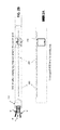
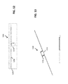
- Figure 12 schematically illustrates an electrical activity sensor 1200 in accordance with a sixth embodiment of the invention.
- the antenna assembly 1200 comprises an RFID sensor 1201 operating in a similar manner to the RFID sensor 201 of the first embodiment and a dipole type antenna 1250 operating in a similar manner to the dipole type antenna 250 of the first embodiment of the invention.
- the dipole type antenna 1250 is folded into a rectangular like shape and arranged alongside the loop antenna 1210 of the RFID sensor 1201.
- FIG. 13 schematically illustrates an electrical activity sensor 1300 in accordance with a seventh embodiment of the invention.
- the electrical activity sensor 1300 comprises an RFID sensor 1301 operating in a similar manner to the RFID sensor 201 of the first embodiment and a dipole type antenna 1350 operating in a similar manner to the dipole type antenna 250 of the first embodiment of the invention.
- the dipole type antenna 1350 extends along the power cable with part of the dipole type antenna being arranged around three sides of the loop antenna 1310 of the RFID sensor 1301. This increases the coupling between the loop antenna 1310 and the dipole type antenna 1350.
- FIG 14 is a block diagram schematically illustrating an electrical activity monitoring apparatus 300 in accordance with an embodiment of the invention.
- the electrical activity monitoring apparatus 300 comprises an RFID reader device 310 and a monitoring device 320 for processing RFID data signals.
- the RFID reader device 310 is a far field RFID type reader and is configured to wirelessly receive RFID data signals transmitted from the electrical activity sensors attached to the power cables 102 of the network via wireless transmission from the respective dipole type antenna 250 and to send RFID interrogation signals to the RFID sensors 200 via wireless transmission to the respective dipole type antennas 250.
- Monitoring device 320 receives data from the RFID reader device 310 indicative of the electrical activity status of the electrical devices 101_1 to 101_n in the electrical activity monitoring system 100.
- the monitoring device 320 is connected to a smart type electricity meter 400 connected to the power supply network 110 of the system.
- the electricity meter 400 and the monitoring 320 device may be connected by a wireless or wired connection.
- the smart electricity meter 400 is configured to monitor the power consumption of electrical devices 101_1 to 101_n connected to the power network 110.
- the smart electricity meter 400 is configured to detect a change in power consumption: for example an increase in the rate of power consumption which may result from the switching ON of one or more electrical devices 101_1 to 101_n supplied by the power network 110, or a decrease in the rate of power consumption which may result from the switching OFF or to STANDBY of one or more of the electrical devices 101_1 to 101_n supplied by the power network 110.
- a command signal is transmitted from the monitoring device 320 to the RFID reader device 310 to activate an RFID reading process.
- the RFID reader device 310 in response to the command signal transmits an interrogation signal to the RFID sensor devices 201_1 to 201_n in order to read the electrical status data stored in the respective RFID memory chips 230_1 to 230_n of the RFID sensor devices 201_1 to 201_n.
- the interrogation signal to be sent from the RFID reader 310 to one or more electrical activity sensors 200s by wireless transmission.
- Response signals are then transmitted by the electrical activity sensors 200_1 to 200_n towards the monitoring apparatus 300 by means of the respective dipole type antennas 250.
- the response signals from the RFID sensor devices 200_1 to 200_n each include the identification code of the respective electrical devices 102_1 to 102_n and the corresponding electrical power state change information stored in the respective RFID memory chip 230.
- the collected electrical power state change information signals are received and read by the RFID reader device 310.
- the processed electrical power state change activity information is then transmitted to the monitoring device 320.
- Monitoring device 310 may further process the received power state change information or transfer the power state change information to another device, such as a remote device connected via a communication network.
- an electrical device 101_x for example a coffee machine
- a household power supply network 110 is switched ON (for example from an OFF power state or from a STANDBY mode):
- the increase in power consumption measured by the smart electricity meter 400 may be detected by the monitoring device 320.
- a read command is sent to the RFID reader device 300 to trigger a read phase of the RFID reader device 310.
- the RFID reader module 310 reads all the RFID sensor devices 201_1 to 201_n of the electrical devices 101_1 to 101_n connected to the power network 110 by transmitting interrogation signals.
- the read information of each RFID sensor 201_1 and includes its identification and its electrical ON/OFF change status.
- the state of the respective state bit signal stored on the corresponding RFID memory chip can be used to identify which electrical device or devices have been switched on or off.
- an electrical pulse generated by an ON to OFF or STANDBY electrical power state change may be distinguished from an electrical pulse generated by an OFF or STANDBY to ON electrical power state change by characterizing the pulse signals.
- the impulse detector 220 of the RIFD sensor device 201 of such embodiments is configured to detect from the characteristics of the generated electrical pulse signal whether the electrical pulse results from an ON to OFF or STANDBY power state change or from an OFF or STANDBY to ON power state change.
- the impulse detector may be configured to distinguish between an OFF to ON and a STANDBY to ON; and to distinguish between an ON to STANDBY and an ON to OFF, by characterizing the resulting pulse signals.
- the power consumed by an electrical device 101_x may be determined, for example by detecting an OFF to ON power state change or a standby to ON power state change and then determining the duration of time for which the electrical device is placed in an ON state. Data representative of the power consumption may then be transferred from the corresponding RFID sensor device 200_x to the RFID reader device 300 by the antenna assembly in the same way as data representative of the electrical power state change is transmitted to the RFID reader device 300.
- the electrical power state change data or consumption data may be processed to provide relevant information on electrical activity of the power network 110, such as for example to build a household user profile, to detect and warn of increased electrical power consumption, and/or to provide recommendations for reducing energy consumption
- the RFID reader may send interrogation signals automatically to the RFID sensor devices without being commanded by the monitoring device; for example on a periodic basis.
- monitoring device may be part of a home gateway system connected to an external internet network.
- Real time tracking of the total home power consumption could be provided by the home electricity provider via the internet network.
- the electricity provider could trigger reading phases of the RFID reader by transmitting signals from a remote server via the gateway device.
- FIG. 15 is a schematic functional block diagram of an RFID sensor device 701 in accordance with a further embodiment of the invention.
- the RFID sensor device 700 comprises a loop antenna 710, a pulse detection module 720 and a memory chip 730 for storing identification data of the RFID sensor and data representative of an electrical status change. These elements operate in a similar way to corresponding elements of the embodiment of Figure 3 .
- the RFID sensor device 700 further includes a timer 740.
- the timer 740 is used to measure the duration of time for which the electrical device has been changed electrical state by measuring the amount of time from when a pulse was detected by the pulse detector 720.
- the time data may be stored in memory 730 and transmitted with the ID data and electrical status data to the RFID reader. The timing data enables the amount of time a device has been switched on or off to be determined.
Abstract
Description
- The present invention relates to an electrical activity sensor device for detecting the electrical activity of an electrical device connected to a power supply network, in particular the change in electrical power state and to an electrical activity monitoring apparatus for monitoring the electrical activity of one or more electrical devices. The electrical activity sensor device is based on a radio frequency identification device (RFID).
- The monitoring of electrical activity of electrical devices finds many useful applications in areas such as energy consumption, building user activity profiles, and security or safety monitoring systems. For example, in a home environment knowledge of the activity of electrical appliances such as washing machines, lighting devices; cookers, toaster or a coffee machine may provide useful information on the household habits and user activity enabling a profile to be built up.
- A known solution for monitoring the activity of electrical devices employs a complex electrical meter system based on remote controlled modules plugged into power outlets and configured to measure the electrical consumption of the electrical equipment powered from the respective power outlet. Such, remote controlled modules are typical equipped with a wireless communication system generally based on low power wireless technology to remotely monitor and control the corresponding electrical appliance. Such advanced meter systems require however a complex and expensive customized installation. Indeed, a recent research report on home automation and monitoring indicated price and technical complexity as being the main market hurdles and inhibitors against widespread adoption. Another drawback of such techniques is that electrical devices may be moved from one power outlet to another power outlet. Moreover some devices such as lighting devices are not always powered from a power outlet.
- Other solutions for the detection of the activity of electrical devices are based on sensing their "EMI (electromagnetic interference) signature" by monitoring the powerlines at one or several points of the power supply network. These techniques require however a customised calibration and training process to learn the EMI signature of various devices. Moreover the EMI signatures may evolve with time. Complex signal processing techniques are required to disaggregate the signatures of the various active devices connected to the network and the obtained results are not always very accurate.
- The present invention has been devised with the foregoing in mind.
- In a general form the invention concerns an electrical activity sensor device based on a radio frequency identification device (RFID).
- According to a first aspect of the invention there is provided an electrical activity sensor attachable to a power cable of an electrical device for detecting an impulse generated in the power cable in response to a change in electrical power state of the electrical device, the electrical activity sensor comprising an antenna assembly including an RFID tag comprising an antenna element operable to magnetically couple with an electrical pulse generated in the power cable to induce an electrical signal in response to a change in electrical power state of the electrical device; and an RFID circuit; and at least one dipole type antenna configured operate as a half wave dipole in the operating frequency range of the RFID tag and to magnetically couple to the antenna element wherein the dipole type conductor is operable to wirelessly transmit data representative of the power state change of the electrical device from the RFID tag to a remote RFID reader.
- Detection of electrical activity can thus be provided in a simplified and low cost manner. The antenna assembly has a dual function of electrical activity detection and transmission of electrical activity data. The operational range of the RFID sensor device is extended since data is transmitted to an RFID reader via the dipole conductor antenna. Improved coupling is provided with the electrical pulse of the power cable since interference from the wires of the power cable is reduced. Moreover the antenna assembly is less susceptible to changes in the form of the power cable.
- A change in the electrical power state of a device may include the switching ON of the device, the switching OFF of the device, the switching from a standby mode to an ON power state, and the switching from an ON power state to a standby mode.
- In an embodiment, the antenna element is a loop antenna.
- In an embodiment, the antenna element is coupled to the dipole type antenna at a coupling distance x from one end of the dipole type antenna, the coupling distance being based upon the input impedance of the RFID circuit.
- Taking into account the input impedance of the RFID circuit helps to reduce the effect of interference from wires in the cable.
- In one embodiment, the coupling distance x is such that the input impedance of the antennas of the antenna assembly matches the input impedance of the RFID circuit.
- In one embodiment, the coupling distance x is based upon the radiation resistance of the dipole type antenna.
- In one embodiment, the coupling distance x is such as to increase the radiation resistance of the dipole conductor
- In one embodiment, the size of the antenna element is adjusted according to the input impedance of the RFID circuit at the RF operating frequency.
- In one embodiment, the distance between the antenna element and the dipole type antenna is adjusted according to the input impedance of the RFID circuit at the RF operating frequency.
- In one embodiment, the dipole type antenna is formed in a helical shape. In one example the helical shape size is such that a single turn helix is provided when the dipole type antenna is wrapped around the cable.
- In one embodiment, a plurality of dipole type antennas are provided, with at least one dipole type antenna being arranged on each side of loop antenna
- In one embodiment, the dipole type antennas are arranged parallel to one another and overlap at least partially
- In one embodiment, the dipole type antenna has at least one fold in its shape.
- In an embodiment, the dipole type antenna is arranged to extend along at least two sides of the antenna element. For example part of the dipole type antenna may be folded around three sides of the antenna element.
- In an embodiment, the RFID tag device comprises a near field RFID tag. The use of a short range (near field) RFID tag combined with wireless transmission by the dipole type antenna enables power consumption to be reduced with respect to a long range (far field) RFID tag while enabling extended coverage to be provided by the dipole conductor.
- In an embodiment, the RFID tag is operable as a passive RFID tag powered by electromagnetic induction via the power cable. This enables power consumption to be reduced by avoiding the use of batteries.
- The data representative of the power state change of the electrical device may comprise identification data identifying the RFID tag. For example the identification data may be enough to indicate an electrical power state change. In other embodiments the data representative of the power state change may be transmitted in addition to the RFID tag identification data.
- A second aspect of the invention relates to an electrical activity monitoring apparatus for monitoring the electrical power status of at least one electrical device connected to a power supply network by a respective power cable and, the electrical activity monitoring apparatus comprising:
- an RFID reader module for reading RFID data from at least one RFID tag device, each RFID tag device being attached to a respective power cable of an electrical device wherein the RFID data is received from the respective RFID tag via wireless transmission from a dipole type antenna magnetically coupled to an antenna of the RFID tag device and the RFID data is representative of electrical power status change of the electrical device; and
- a monitor device for determining from the RFID data received by the RFID reader module, which electrical devices of the network have changed electrical power status.
- In an embodiment, the RFID reader module is configured to read signals from the at least one RFID tag in response to a detected change in power consumption measured by an electricity meter connected to the power supply network.
- In an embodiment, a communication network interface is provided for connecting with a communication network such that data may be transmitted to or received from a remote server connected to the communication network.
- A further aspect of the invention relates to a gateway device comprising electrical activity monitoring apparatus according to the second aspect of the invention.
- In an embodiment the RFID reader module is configured to trigger the transmission of one or more interrogation signals in response to a command signal received via the communication network.
- According to a further aspect of the invention there is provided an electrical activity monitoring system comprising at least one electrical activity sensor according to any embodiment of the first aspect of the invention for monitoring the electrical status of an electrical device, and an electrical activity monitoring apparatus according to any embodiment of the second aspect of the invention.
- In an embodiment the electrical activity monitoring system further includes an electricity meter connected to the electrical activity monitoring apparatus for monitoring electrical power consumption in the power supply network.
- In an embodiment the RFID reader module is configured to transmit interrogation signal to the RFID tag devices in response to a detected change in power consumption measured by the electricity meter.
- In some embodiments of the invention timing means are provided to determine how long an electrical appliance has been switched ON or switched OFF.
- According to a further aspect of the invention there is provided an antenna assembly attachable to a power cable of an electrical device for detecting an impulse generated in the power cable in response to a change in electrical power state of the electrical device, the an antenna assembly including an antenna element, for example a loop antenna, operable to magnetically couple with an electrical pulse generated in the power cable to induce an electrical signal in response to a change in electrical power state of the electrical device; and at least one dipole type antenna configured operate as a half wave dipole in the operating frequency range of the antenna element and to magnetically couple to the antenna element wherein the dipole type conductor is operable to wirelessly transmit data representative of the power state change of the electrical device from the antenna assembly to a remote RFID reader.
- Some processes implemented by elements of the invention may be computer implemented. Accordingly, such elements may take the form of an entirely hardware embodiment, an entirely software embodiment (including firmware, resident software, micro-code, etc.) or an embodiment combining software and hardware aspects that may all generally be referred to herein as a "circuit", "module" or "system'. Furthermore, such elements may take the form of a computer program product embodied in any tangible medium of expression having computer usable program code embodied in the medium.
- Since elements of the present invention can be implemented in software, the present invention can be embodied as computer readable code for provision to a programmable apparatus on any suitable carrier medium. A tangible carrier medium may comprise a storage medium such as a floppy disk, a CD-ROM, a hard disk drive, a magnetic tape device or a solid state memory device and the like. A transient carrier medium may include a signal such as an electrical signal, an electronic signal, an optical signal, an acoustic signal, a magnetic signal or an electromagnetic signal, e.g. a microwave or RF signal.
- Embodiments of the invention will now be described, by way of example only, and with reference to the following drawings in which:
-
FIG. 1 is a schematic block diagram of an electrical activity monitoring system in which one or more embodiments of the invention may be implemented -
FIG. 2A is a schematic diagram of an electrical activity sensor device in accordance with a first embodiment of the invention; -
FIG. 2B is a schematic diagram of the electrical activity sensor device ofFIG. 2A mounted on a power cable; -
FIG. 3 is a block diagram of an RFID sensor device in accordance with an embodiment of the invention; -
FIG. 4A is a block functional diagram of elements of a RFID sensor device in accordance with an embodiment of the invention; -
FIG. 4B is a graphical diagram illustrating a signal processing process implemented by an RFID sensor in accordance with an embodiment of the invention; -
FIG. 5A graphically illustrates current voltage and magnetic field distributions along a half-wave dipole; -
FIG. 5B schematically illustrates an arrangement of a half-wave dipole and a loop antenna; -
FIG. 6A graphically illustrates an example of simulated antenna input impedance for an antenna assembly in free space; -
FIG. 6B graphically illustrates an example of simulated antenna pattern in two orthogonal planes for an antenna assembly in free space; -
FIG. 7A graphically illustrates an example of simulated antenna pattern in two orthogonal planes for an antenna assembly in the presence of a power cable; -
FIG. 7B graphically illustrates an example of simulated antenna input impedance for an antenna assembly in the presence of a cable; -
FIG. 8 is a schematic diagram of an electrical activity sensor device in accordance with a second embodiment of the invention; -
FIG. 9 is a schematic diagram of an electrical activity sensor device in accordance with a third embodiment of the invention; -
FIG. 10 is a schematic diagram of an electrical activity sensor device in accordance with a fourth embodiment of the invention; -
FIG. 11 is a schematic diagram of an electrical activity sensor device in accordance with a fifth embodiment of the invention; -
FIG. 12 is a schematic diagram of an electrical activity sensor device in accordance with a sixth embodiment of the invention; -
FIG. 13 is a schematic diagram of an electrical activity sensor device in accordance with a seventh embodiment of the invention; -
FIG. 14 is a schematic block diagram of an electrical activity monitoring apparatus in accordance with an embodiment of the invention; and -
FIG. 15 is a schematic block diagram of an RFID sensor device in accordance with a further embodiment of the invention. -
Figure 1 is a schematic block diagram of an electrical activity monitoring system in which one or more embodiments of the invention may be implemented. The electricalactivity monitoring system 100 monitors the change in electrical status of n electrical devices 101_1 to 101_n. Each electrical device 101_1 to 101_n is connected by means of a respective electrical power cable 102_1 to 102_n to a power outlet 103_1 to 103_n of an electricalpower supply network 110. It will be appreciated that while in the illustrated embodiment ofFigure 1 each electrical device 101_1 to 101_n is connected to a respective power outlet 103_1 to 103_n, in other embodiments of the invention a plurality of electrical devices may be connected to the same power outlet 103_x. - Each electrical power cable 102_1 to 102_n is provided with a respective plug 104_1 to 104_n for connecting the respective electrical power cable to a respective power outlet 103_1 to 103_n for connection to the
power supply network 110. - Each electrical power cable 102_1 to 102_n is further provided with a respective electrical activity sensor 200_1 to 200_n. Each electrical activity sensor 2000_1 to 2000_n is attached to a respective power cable 102_1 to 102_n. The electrical activity sensor 2000_1 to 2000_n comprises an antenna assembly.
- The electrical
activity monitoring system 100 further includes an electricalactivity monitoring apparatus 300. Thepower supply network 110 is typically provided with anelectricity meter 400 for measuring electrical consumption in thepower supply network 110. The electricalactivity monitoring apparatus 300 may be connected to a communication network NET such as an Internet network so that data on the electrical activity of the system may be transmitted to a remote device, such as a remote electrical activity monitoring device for example the server of a remote an electrical activity monitoring service or an electricity power supplier company. -
Figure 2A schematically illustrates an electrical activity sensor in accordance with an embodiment of the invention. Theelectrical activity sensor 200 comprises an antenna assembly including anRFID sensor 201 and adipole type antenna 250 provided on aflexible substrate 280. The antenna assembly may, for example be etched on theflexible support layer 280. Theflexible support layer 280 may for example be a thin Polystyrene adhesive film. - With reference to
Figure 2A theRFID sensor 201 in accordance with an embodiment of the invention comprises aloop antenna 210 and an RFID circuit 202. The RFID circuit 202 is provided with apulse detection module 220 and amemory chip 230 for storing data representative of an electrical status change and/or identification data identifying theRFID sensor 201. EachRFID sensor device 201 in theelectrical monitoring system 100 is provided with an identification code enabling it to be identified by themonitoring device 300. An RFID sensor may also be referred to as an RFID tag, an RFID label, an RFID transponder and the like. While the loop antenna in the present embodiment is presented as a rectangular or square shape it will be appreciated that any form of loop antenna may be used. - The
RFID sensor 201 may for example be a near field/short range RFID tag operating in the UHF frequency band, for example in the range from 800 MHz to 960 MHz, such as the region of 860 MHz or 900 MHz, or in the region of 433MHz; or operating in the HF frequency band, for example in the region of 13.6MHz. - RFID may be considered as a non-specific short range device. It can use frequency bands without a license. Nevertheless, RFID should typically be compliant with local regulations (ETSI, FCC etc.)
- LF: 125 kHz - 134,2 kHz : low frequencies,
- HF: 13.56 MHz : high frequencies,
- UHF: 860 MHz - 960 MHz : ultra high frequencies,
SHF: 2.45 GHz : super high frequencies - The
loop antenna 210 of theRFID sensor device 201 has a dual function. Firstly, theantenna 210 of an RFID sensor device 200_x is used to detect the electrical pulse generated in the respective power cable 102_x when the corresponding electrical device 101_x undergoes a change in electrical power state, for example is switched ON or switched OFF. Indeed, the generated electrical pulse results from the change in power state of the respective electrical device 101_x. When an electrical device 101_x is switched ON or OFF, a current pulse flows in its respective power cable 102_x. Theloop antenna 210 of the respective RFID sensor device 200_x attached to the power cable 102_x couples magnetically to the current pulse generating an electrical pulse which can be detected by thepulse detection module 220. The electric state change is stored in theRFID chip memory 230. - The second function of the
antenna 210 is to electromagnetically couple the dipole-type antenna 250 to the RFID circuit 202. - The
dipole type antenna 250 comprises a half-wave length dipole-type conductor having a length L, sized, to operate in the RF operating frequency range of theRFID sensor 200. -
Figure 2B schematically illustrates the antenna assembly ofFigure 2A attached to thepower cable 102 of an electrical device 101. - The
power cable 102 comprises an insulatingsheath 112 enclosing a plurality of conducting wires W for providing power from thepower supply network 110 to the corresponding electrical device 101. - The
flexible substrate 280 is wrapped at least partially around thepower cable 102 and adheres by means of adhesive to the insulatingsheath 112. Theloop antenna 210 of the RFID sensor is wrapped at least partially around thepower cable 102. Thedipole type antenna 250 extends along thepower cable 102, with part of thedipole antenna 250 extending between opposing ends of theloop antenna 210 wrapped around thepower cable 102 to enable magnetic coupling between theloop antenna 210 and thedipole type antenna 250. - In order to enable the maximum transfer of RF energy between the
RFID sensor 201 and thedipole type antenna 250, the half-wave dipole of the dipole likeantenna 250 is magnetically coupled to theloop antenna 210 of theRFID sensor 200 in an impedance plane of the resonating dipole for which the radiation impedance of the half-wave dipole 250 (in presence of the power cable wires) transformed through the wire loop is almost equal to the real part of theRFID circuit 220. - In this way the dipole-
type antenna 250 coupled to theloop antenna 210 behaves as an efficient half-wave dipole at the operating frequency of theRFID sensor 201 despite the very close proximity of the wires W of thepower cable 102. -
Figure 4A is a schematic diagram illustrating an example of operation of thepulse detection module 220 of theRFID sensor 201. When the electrical power state of an electrical device changes, for example by being switched ON or OFF a corresponding power state change pulse signal A is picked up by theloop antenna 210, by means of a magnetic coupling effect. When the amplitude of the power state change pulse signal A exceeds a predetermined threshold (1V for example), ablock comparator 221 detects an input pulse signal and in response changes the state of the output signal B. In order to avoid multi triggering, atemporization device 222 may be connected to the output of thecomparator 221 to provide a signal C at its output which corresponds to the signal issued from the comparator during a set temporization time. A Dflip flop module 223 generates a state bit D. The state bit D is changed for each clocked impulse since the DFlip Flop module 223 is clocked by the output signal C of thetemporization module 222. Consequently the last bit of bit signal D changes state at each detected pulse (at switch on or off). The state can thus be used to indicate an electrical power state change. The bit value is stored in thememory chip 230 of theRFID sensor device 201. This information representative of a change of electrical power state of respective electrical device 101_x can then be transmitted with the identification code IDRFID sensor device 200 to themonitoring device 300 by theantenna assembly 200. An example of signals A, B, C and D of the operation ofFigure 4A are graphically represented inFigure 4B . - In particular embodiments of the invention by knowing the initial electrical power state of the electrical device 101_x at counter reset, it is possible to determine from the state of bit signal D whether the electrical change corresponds to an ON/OFF electrical status change or an OFF/ON electrical status change. Moreover, by knowing the ON or OFF power state of the electrical device at the previous reading the ON or OFF power state at the subsequent reading can be deduced.
- When activated by an electrical power state change, the
loop antenna 210 of theRFID sensor 201 transfers data indicative of an electrical state change from thememory chip 222 to the dipole-type antenna 250 and the data is transmitted wirelessly from theelectrical activity sensor 200 to theRFID reader 310 of themonitoring device 300 by the radiatingdipole type antenna 250. - Data representative of the electrical state change may be transferred by the
electrical activity sensor 200 to theRFID reader 310, for example at each interrogation by the RFID reader operating in the RFID frequency band. - In the case where the
RFID sensor 201 is a passive type RFID tag theantenna 210 acts as a power-coupling inductor which can harvest electrical power from the coupling between theloop antenna 210 and the electrical pulse generated in thepower cable 102 to operate the modules of theRFID sensor device 200, such as thememory chip 230 and thepulse detection module 220. Since theRFID sensor 201 in such an embodiment is a passive RFID tag device, energy consumption can be minimized since power is not being supplied constantly to theRFID sensor 201 from a power supply such as a battery. It will be appreciated, however, that in alternative embodiments of the invention theRFID sensor 201 may be an active type RFID tag powered by its own power supply means or a battery assisted passive type RFID tag. - The
electrical activity sensor 200 may be attached to the respective power cable 102_x by any form of fixation means such as for example by adhesive such as glue, sticking tape, or a sticker, by a mechanical connection such as for example staples, screws, nails; or by being embedded in the insulatingsheath cover 112 of the respective power cable 102_x. -
Figure 5A graphically illustrates current and voltage distributions along a half-wave dipole and the corresponding magnetic field. The magnetic field is maximum at the middle of the dipole and minimum at the edges. Thus, when in free space, the optimum magnetic coupling of thedipole type antenna 250 to theloop antenna 210 of theRFID sensor 201 would be obtained at the center of the dipole as illustrated inFigure 5B . The inductive coupling between theloop antenna 210 and the resonantdipole type antenna 250 may be modeled, for example by a transformer with a mutual inductance of M. In this way the input impedance of the antenna assembly Za at the edges of the loop may be expressed as:
antenna assembly 200, Zloop represents the impedance of theloop antenna 210 which is mainly inductive and generally equal to the loop inductance at the resonant frequency, Zr is the dipole radiation resistance of a symmetrical dipole (i.e. dipole excited at its center). - For optimal matching to the impedance of the RFID circuit 202, the real and imaginary part of the input impedance of the
antenna assembly 200 should be the conjugate of the impedance of the RFID circuit 202. For example, a typical input impedance of an RFID circuit is equivalent to an RC parallel circuit with R ≈1 to 2 kΩ and C ≈1 to 2 pF, giving typical values of Ra ≈10 Ω and Xa ≈-100 Ω at an operating frequency of 900 MHz. Thus, in this example the size of theloop antenna 210 and the distance between theloop antenna 210 and thedipole type antenna 250 may be adjusted so that Za= Ra + jXa is approximately equal to 10 Ω + jx100 Ω at 900 MHz. -
Figure 6A graphically illustrates an example of simulated real (R1) and imaginary (X1) parts of the input impedance of the antenna assembly ofFigure 5B , comprising a dipole type antenna of length 16.5 cm excited through an inductive square loop antenna having 1cm sides with a 2mm gap between the loop antenna and the dipole type antenna.Figure 6B graphically illustrates the corresponding radiation patterns generated in 2 orthogonal planes. These results show fairly good matching of typical RFID circuits over a relatively wide frequency bandwidth and a typical dipole radiation pattern. However, when the antenna assembly is wrapped around the power cable as shown inFigure 2B , while the radiation pattern remains almost unchanged as graphically illustrated inFigure 7A , the input impedance of the antenna assembly is significantly modified with a sensitive reduction in the frequency matching bandwidth to the RFID circuit and a dramatic increase of the real part of the antenna input as graphically illustrated inFigure 7B . - In order to better match the input impedance of the antennas of the antenna assembly to the RFID circuit, the real part of the input impedance of the antenna assembly should be significantly reduced. With reference to equation (1) that means that the radiation resistance Zr of the dipole type antenna should be significantly increased.
Knowing that the radiation resistance Zr of a half-wave dipole driven at a distance x from its end is expressed as:
where: - o R0= radiation resistance when the dipole is driven at its center; theoretically equal to 73Ω for an infinitely thin dipole
- o λ= wavelength at resonant frequency
- The idea is to adjust the radiation resistance Zr of the
dipole type antenna 250 to any arbitrary value greater than 73 Ω by moving the driving point position corresponding to position of the coupling with theloop antenna 210 from the center of thedipole type antenna 250 towards one end of thedipole type antenna 250 as illustrated inFigures 2A and 2B . - Accordingly based on the above observations in embodiments of the invention the
loop antenna 210 is coupled to thedipole type antenna 250 at coupling position located at a distance x from the end of thedipole type antenna 250 based upon the input impedance of the RFID circuit 202. In this way the dipole-type conductor 250 coupled to theloop antenna 210 behaves as an efficient half-wave dipole at the UHF working frequency) despite the very close proximity of the 2 or 3 wires of the power supply. - In a preferred embodiment the
loop antenna 210 is coupled to thedipole type antenna 250 at a distance x from the end of thedipole conductor 250 so that the input impedance of the antenna assembly matches the input impedance of theRFID circuit 220. In particular theloop antenna 210 is coupled to thedipole type antenna 250 at a distance x from the end of thedipole conductor 250 based upon the radiation resistance of thedipole conductor 250. Preferably the loop antenna is coupled to the dipole at a coupling position located a distance x from the end of the dipole conductor to increase the radiation resistance Zr of thedipole conductor 250. -
Figure 8 schematically illustrates anelectrical activity sensor 800 in accordance with a second embodiment of the invention. Theelectrical activity sensor 800 comprises an RFID sensor 801 and adipole type antenna 850 operating in a similar manner to theRFID sensor 201 and thedipole type antenna 250 of the first embodiment of the invention. In the second embodiment thedipole type antenna 850 has a helical shape, in particular with a sizing providing a single turn helix when wrapped around therespective power cable 102. In this embodiment the symmetry of the radiation pattern of the dipole type antenna is improved. - In further embodiments of the invention, the antenna assembly may comprise a plurality of dipole type conductor antennas. For example,
Figure 9 schematically illustrates anelectrical activity sensor 900 in accordance with a third embodiment of the invention. Theelectrical activity sensor 900 comprises an RFID sensor 901 operating in a similar manner to theRFID sensor 201 of the first embodiment and a plurality ofdipole type antennas dipole type antenna 250 of the first embodiment of the invention. In the third embodiment twodipole type antennas loop antenna 910 of theRFID sensor 900. The twodipole type antennas dipole type antennas -
Figure 10 schematically illustrates anelectrical activity sensor 1000 in accordance with a fourth embodiment of the invention. Theelectrical activity sensor 1000 comprises an RFID sensor 1001 operating in a similar manner to theRFID sensor 201 of the first embodiment and a plurality ofdipole type antennas dipole type antenna 850 of the second embodiment of the invention. In the fourth embodiment twodipole type antennas loop antenna 1010 of the RFID sensor 1001. The twodipole type antennas respective power cable 102. The twodipole type antennas -
Figure 11 schematically illustrates anelectrical activity sensor 1100 in accordance with a fifth embodiment of the invention. Theelectrical activity sensor 1100 comprises an RFID sensor 1101 operating in a similar manner to theRFID sensor 201 of the first embodiment and a plurality ofdipole type antennas dipole type antenna 250 of the first embodiment of the invention. In the fifth embodiment twodipole type antennas loop antenna 1110 of the RFID sensor 1101. The twodipole type antennas respective power cable 102. The twodipole type antennas - In further embodiments of the invention the dipole type antenna may be formed as a dipole conductor with at least one fold. The radiation resistance of a folded dipole is greater than the radiation resistance of a classical half-wave dipole, Depending on the folding configuration the radiation resistance may be four times that of a classical half-wave dipole. That helps to increase the dipole radiation resistance in the presence of the power cable to improve the coupling. For example
Figure 12 schematically illustrates anelectrical activity sensor 1200 in accordance with a sixth embodiment of the invention. Theantenna assembly 1200 comprises an RFID sensor 1201 operating in a similar manner to theRFID sensor 201 of the first embodiment and adipole type antenna 1250 operating in a similar manner to thedipole type antenna 250 of the first embodiment of the invention. In the sixth embodiment thedipole type antenna 1250 is folded into a rectangular like shape and arranged alongside theloop antenna 1210 of the RFID sensor 1201. -
Figure 13 schematically illustrates anelectrical activity sensor 1300 in accordance with a seventh embodiment of the invention. Theelectrical activity sensor 1300 comprises an RFID sensor 1301 operating in a similar manner to theRFID sensor 201 of the first embodiment and adipole type antenna 1350 operating in a similar manner to thedipole type antenna 250 of the first embodiment of the invention. In the seventh embodiment thedipole type antenna 1350 extends along the power cable with part of the dipole type antenna being arranged around three sides of theloop antenna 1310 of the RFID sensor 1301. This increases the coupling between theloop antenna 1310 and thedipole type antenna 1350. -
Figure 14 is a block diagram schematically illustrating an electricalactivity monitoring apparatus 300 in accordance with an embodiment of the invention. The electricalactivity monitoring apparatus 300 comprises anRFID reader device 310 and amonitoring device 320 for processing RFID data signals. - The
RFID reader device 310 is a far field RFID type reader and is configured to wirelessly receive RFID data signals transmitted from the electrical activity sensors attached to thepower cables 102 of the network via wireless transmission from the respectivedipole type antenna 250 and to send RFID interrogation signals to theRFID sensors 200 via wireless transmission to the respectivedipole type antennas 250. -
Monitoring device 320 receives data from theRFID reader device 310 indicative of the electrical activity status of the electrical devices 101_1 to 101_n in the electricalactivity monitoring system 100. - In one particular embodiment of the invention the
monitoring device 320 is connected to a smarttype electricity meter 400 connected to thepower supply network 110 of the system. Theelectricity meter 400 and themonitoring 320 device may be connected by a wireless or wired connection. Thesmart electricity meter 400 is configured to monitor the power consumption of electrical devices 101_1 to 101_n connected to thepower network 110. Thesmart electricity meter 400 is configured to detect a change in power consumption: for example an increase in the rate of power consumption which may result from the switching ON of one or more electrical devices 101_1 to 101_n supplied by thepower network 110, or a decrease in the rate of power consumption which may result from the switching OFF or to STANDBY of one or more of the electrical devices 101_1 to 101_n supplied by thepower network 110. In response to the detected change in power consumption a command signal is transmitted from themonitoring device 320 to theRFID reader device 310 to activate an RFID reading process. TheRFID reader device 310 in response to the command signal transmits an interrogation signal to the RFID sensor devices 201_1 to 201_n in order to read the electrical status data stored in the respective RFID memory chips 230_1 to 230_n of the RFID sensor devices 201_1 to 201_n. The interrogation signal to be sent from theRFID reader 310 to one or more electrical activity sensors 200s by wireless transmission. Response signals are then transmitted by the electrical activity sensors 200_1 to 200_n towards themonitoring apparatus 300 by means of the respectivedipole type antennas 250. The response signals from the RFID sensor devices 200_1 to 200_n each include the identification code of the respective electrical devices 102_1 to 102_n and the corresponding electrical power state change information stored in the respectiveRFID memory chip 230. The collected electrical power state change information signals are received and read by theRFID reader device 310. The processed electrical power state change activity information is then transmitted to themonitoring device 320. -
Monitoring device 310 may further process the received power state change information or transfer the power state change information to another device, such as a remote device connected via a communication network. - For example, if an electrical device 101_x, for example a coffee machine, connected to a household
power supply network 110 is switched ON (for example from an OFF power state or from a STANDBY mode): - 1. The total power consumption will increase by an amount corresponding to the power consumed by the coffee machine. This change in power consumption will be measured by
smart electricity meter 400. - 2. The current impulse generated in the corresponding power cable in response to the switch on activates the corresponding
RFID sensor device 201 attached to the respective power cable, and the status information change (OFF to ON) is stored in the RFID memory chip by switching a bit (the "state bit") from 0 (corresponding to OFF state) to 1 (corresponding to ON state) - The increase in power consumption measured by the
smart electricity meter 400 may be detected by themonitoring device 320. In response to the detected increase a read command is sent to theRFID reader device 300 to trigger a read phase of theRFID reader device 310. TheRFID reader module 310 reads all the RFID sensor devices 201_1 to 201_n of the electrical devices 101_1 to 101_n connected to thepower network 110 by transmitting interrogation signals. The read information of each RFID sensor 201_1 and includes its identification and its electrical ON/OFF change status. - In some embodiments of the invention by comparing the electrical change status of all the RFID sensor devices read with the previous one stored in an electrical devices status dataset, at the previous reading phase, it is possible to infer which electrical device has been powered on and the electrical devices status dataset may be updated accordingly.
- In other embodiments of the invention, the state of the respective state bit signal stored on the corresponding RFID memory chip can be used to identify which electrical device or devices have been switched on or off.
- In some particular embodiments of the invention for an electrical device an electrical pulse generated by an ON to OFF or STANDBY electrical power state change, may be distinguished from an electrical pulse generated by an OFF or STANDBY to ON electrical power state change by characterizing the pulse signals. The
impulse detector 220 of theRIFD sensor device 201 of such embodiments is configured to detect from the characteristics of the generated electrical pulse signal whether the electrical pulse results from an ON to OFF or STANDBY power state change or from an OFF or STANDBY to ON power state change. - In further embodiments the impulse detector may be configured to distinguish between an OFF to ON and a STANDBY to ON; and to distinguish between an ON to STANDBY and an ON to OFF, by characterizing the resulting pulse signals.
- In another embodiment of the invention the power consumed by an electrical device 101_x may be determined, for example by detecting an OFF to ON power state change or a standby to ON power state change and then determining the duration of time for which the electrical device is placed in an ON state. Data representative of the power consumption may then be transferred from the corresponding RFID sensor device 200_x to the
RFID reader device 300 by the antenna assembly in the same way as data representative of the electrical power state change is transmitted to theRFID reader device 300. - The electrical power state change data or consumption data may be processed to provide relevant information on electrical activity of the
power network 110, such as for example to build a household user profile, to detect and warn of increased electrical power consumption, and/or to provide recommendations for reducing energy consumption - In other embodiments of the invention, rather than sending an interrogation signal from the RFID reader to the RFID sensor devices in response to a command from the
monitoring device 320 the RFID reader may send interrogation signals automatically to the RFID sensor devices without being commanded by the monitoring device; for example on a periodic basis. - In some embodiments of the system that monitoring device may be part of a home gateway system connected to an external internet network. Real time tracking of the total home power consumption could be provided by the home electricity provider via the internet network. For example the electricity provider could trigger reading phases of the RFID reader by transmitting signals from a remote server via the gateway device.
-
Figure 15 is a schematic functional block diagram of an RFID sensor device 701 in accordance with a further embodiment of the invention. - The
RFID sensor device 700 comprises aloop antenna 710, apulse detection module 720 and amemory chip 730 for storing identification data of the RFID sensor and data representative of an electrical status change. These elements operate in a similar way to corresponding elements of the embodiment ofFigure 3 . With respect to the embodiment ofFigure 3 theRFID sensor device 700 further includes atimer 740. Thetimer 740 is used to measure the duration of time for which the electrical device has been changed electrical state by measuring the amount of time from when a pulse was detected by thepulse detector 720. The time data may be stored inmemory 730 and transmitted with the ID data and electrical status data to the RFID reader. The timing data enables the amount of time a device has been switched on or off to be determined. - Although the present invention has been described hereinabove with reference to specific embodiments, the present invention is not limited to the specific embodiments, and modifications will be apparent to a skilled person in the art which lie within the scope of the present invention.
- For instance, while the foregoing examples have been described with respect to a household power network system, it will be appreciated that embodiments of the invention may be applied to any power network to which electrical devices are connected. Moreover the system could be applied in security or safety applications to identify electrical devices which have been switched on or switched off.
- Many further modifications and variations will suggest themselves to those versed in the art upon making reference to the foregoing illustrative embodiments, which are given by way of example only and which are not intended to limit the scope of the invention, that being determined solely by the appended claims. In particular the different features from different embodiments may be interchanged, where appropriate.
Claims (15)
- An electrical activity sensor attachable to a power cable of an electrical device for detecting an impulse generated in the power cable in response to a change in electrical power state of the electrical device, the electrical activity sensor comprising an antenna assembly including
an RFID tag comprising an antenna element operable to magnetically couple with an electrical pulse generated in the power cable to induce an electrical signal in response to a change in electrical power state of the electrical device; the antenna element being provided with an RFID circuit; and
at least one dipole type antenna configured operate as a half wave dipole in the operating frequency range of the RFID tag and to magnetically couple to the antenna element wherein the dipole type conductor is operable to wirelessly transmit data representative of the power state change of the electrical device from the RFID tag to a remote RFID reader. - An electrical activity sensor according to claim 1 wherein the antenna element is a loop antenna.
- An electrical activity sensor according to claim 1 or 2 wherein the antenna element is coupled to the dipole type antenna at a coupling distance x from one end of the dipole type antenna, the coupling distance being based upon the input impedance of the RFID circuit.
- An electrical activity sensor according to claim 3 wherein the coupling distance x is such that the input impedance of the antenna assembly matches the input impedance of the RFID circuit.
- An electrical activity sensor according to claim 3 or 4 wherein the coupling distance x is based upon the radiation resistance of the dipole type antenna.
- An electrical activity sensor according to claim 5 wherein the coupling distance x is such as to increase the radiation resistance of the dipole conductor
- An electrical activity sensor according to any preceding claim wherein the size of the antenna element is adjusted according to the input impedance of the RFID circuit at the RF operating frequency.
- An electrical activity sensor according to any preceding claim wherein the distance between the antenna element and the dipole type antenna is adjusted according to the input impedance of the RFID circuit at the RF operating frequency.
- An electrical activity sensor according to any preceding claim wherein the dipole type antenna is formed in a helical shape
- An electrical activity sensor according to any preceding comprising a plurality of dipole type antennas, with at least one dipole type antenna being arranged on each side of loop antenna
- An electrical activity sensor according to claim 10 wherein the dipole type antennas are arranged to overlap at least partially
- An electrical activity sensor according to any preceding claim wherein the dipole type antenna has at least one fold in its shape.
- An electrical activity sensor according to claim 13 wherein the dipole type antenna is arranged to extend along at least two sides of the antenna element.
- An electrical activity sensor to any preceding claim wherein the RFID tag device comprises a near field RFID tag.
- An electrical activity monitoring apparatus for monitoring the electrical power status of at least one electrical device connected to a power supply network by a respective power cable and, the electrical activity monitoring apparatus comprising:an RFID reader module for reading RFID data from at least one RFID tag device, each RFID tag device being attached to a respective power cable of an electrical device wherein the RFID data is received from the respective RFID tag via wireless transmission from a dipole type antenna magnetically coupled to an antenna of the RFID tag device and the RFID data is representative of electrical power status change of the electrical device; anda monitor device for determining from the RFID data received by the RFID reader module, which electrical devices of the network have changed electrical power status.
Priority Applications (2)
| Application Number | Priority Date | Filing Date | Title |
|---|---|---|---|
| EP14305542.4A EP2930470B1 (en) | 2014-04-11 | 2014-04-11 | Electrical activity sensor device for detecting electrical activity and electrical activity monitoring apparatus |
| US14/679,251 US9824249B2 (en) | 2014-04-11 | 2015-04-06 | Electrical activity sensor device for detecting electrical activity and electrical activity monitoring apparatus |
Applications Claiming Priority (1)
| Application Number | Priority Date | Filing Date | Title |
|---|---|---|---|
| EP14305542.4A EP2930470B1 (en) | 2014-04-11 | 2014-04-11 | Electrical activity sensor device for detecting electrical activity and electrical activity monitoring apparatus |
Publications (2)
| Publication Number | Publication Date |
|---|---|
| EP2930470A1 true EP2930470A1 (en) | 2015-10-14 |
| EP2930470B1 EP2930470B1 (en) | 2017-11-22 |
Family
ID=50555144
Family Applications (1)
| Application Number | Title | Priority Date | Filing Date |
|---|---|---|---|
| EP14305542.4A Not-in-force EP2930470B1 (en) | 2014-04-11 | 2014-04-11 | Electrical activity sensor device for detecting electrical activity and electrical activity monitoring apparatus |
Country Status (2)
| Country | Link |
|---|---|
| US (1) | US9824249B2 (en) |
| EP (1) | EP2930470B1 (en) |
Families Citing this family (4)
| Publication number | Priority date | Publication date | Assignee | Title |
|---|---|---|---|---|
| NZ724281A (en) * | 2014-04-14 | 2018-11-30 | Licensys Australasia Pty Ltd | Vehicle identification and/or monitoring system |
| EP3193140A1 (en) * | 2016-01-15 | 2017-07-19 | Thomson Licensing | Method and apparatus for switch on/off impulse detection |
| EP3240106A1 (en) * | 2016-04-25 | 2017-11-01 | Thomson Licensing | Electrical activity sensor device for detecting electrical activity and electrical activity monitoring apparatus |
| KR20200082251A (en) * | 2018-12-28 | 2020-07-08 | 삼성전자주식회사 | Quasi-isotropic antenna |
Citations (3)
| Publication number | Priority date | Publication date | Assignee | Title |
|---|---|---|---|---|
| US20060109384A1 (en) * | 2002-12-21 | 2006-05-25 | Koninkliklijke Philips Electronics N.V. | Power management in appliances |
| US20090195349A1 (en) * | 2008-02-01 | 2009-08-06 | Energyhub | System and method for home energy monitor and control |
| US20120013442A1 (en) * | 2010-07-16 | 2012-01-19 | Powertech Industrial Co., Ltd. | Power cord |
Family Cites Families (13)
| Publication number | Priority date | Publication date | Assignee | Title |
|---|---|---|---|---|
| GB9626550D0 (en) * | 1996-12-20 | 1997-02-05 | Northern Telecom Ltd | A dipole antenna |
| RU2163739C1 (en) * | 2000-07-20 | 2001-02-27 | Криштопов Александр Владимирович | Antenna |
| US7089089B2 (en) * | 2003-03-31 | 2006-08-08 | Power Measurement Ltd. | Methods and apparatus for retrieving energy readings from an energy monitoring device |
| EP1667336B1 (en) | 2003-09-19 | 2013-05-01 | Brother Kogyo Kabushiki Kaisha | Radio tag reader/writer |
| WO2005112285A1 (en) * | 2004-05-14 | 2005-11-24 | Brother Kogyo Kabushiki Kaisha | Radio communication device |
| WO2008081699A1 (en) * | 2006-12-28 | 2008-07-10 | Philtech Inc. | Base sheet |
| JP5162648B2 (en) * | 2010-12-01 | 2013-03-13 | デクセリアルズ株式会社 | ANTENNA DEVICE AND COMMUNICATION DEVICE |
| WO2012117843A1 (en) | 2011-02-28 | 2012-09-07 | 株式会社村田製作所 | Wireless communication device |
| US20120280828A1 (en) * | 2011-05-02 | 2012-11-08 | Kim Moon J | Rfid-based electricity metering system |
| US9164135B2 (en) * | 2011-09-13 | 2015-10-20 | Honeywell International Inc. | System and method for measuring phase attributes of electrical grid system and equipment using a smart probe |
| WO2013057059A1 (en) | 2011-10-20 | 2013-04-25 | Tyco Electronics Raychem Bvba | Device and method for tagging cables |
| JP5537576B2 (en) * | 2012-01-13 | 2014-07-02 | シャープ株式会社 | Identification adapter, power supply device, and power supply system |
| US9479848B2 (en) * | 2013-11-08 | 2016-10-25 | General Electric Company | System and method for monitoring characteristics of an electrical device |
-
2014
- 2014-04-11 EP EP14305542.4A patent/EP2930470B1/en not_active Not-in-force
-
2015
- 2015-04-06 US US14/679,251 patent/US9824249B2/en not_active Expired - Fee Related
Patent Citations (3)
| Publication number | Priority date | Publication date | Assignee | Title |
|---|---|---|---|---|
| US20060109384A1 (en) * | 2002-12-21 | 2006-05-25 | Koninkliklijke Philips Electronics N.V. | Power management in appliances |
| US20090195349A1 (en) * | 2008-02-01 | 2009-08-06 | Energyhub | System and method for home energy monitor and control |
| US20120013442A1 (en) * | 2010-07-16 | 2012-01-19 | Powertech Industrial Co., Ltd. | Power cord |
Also Published As
| Publication number | Publication date |
|---|---|
| US9824249B2 (en) | 2017-11-21 |
| EP2930470B1 (en) | 2017-11-22 |
| US20150294127A1 (en) | 2015-10-15 |
Similar Documents
| Publication | Publication Date | Title |
|---|---|---|
| EP2916467A2 (en) | Electrical activity sensor device for detecting electrical activity and electrical activity monitoring apparatus | |
| US10003863B2 (en) | Electrical activity sensor device for detecting electrical activity and electrical activity monitoring apparatus | |
| US9893411B2 (en) | Electrical activity sensor device for detecting electrical activity and electrical activity monitoring apparatus | |
| EP2916466B1 (en) | Electrical activity sensor device for detecting electrical activity and electrical activity monitoring apparatus | |
| US9824249B2 (en) | Electrical activity sensor device for detecting electrical activity and electrical activity monitoring apparatus | |
| US8742900B2 (en) | RFID enabled light switches | |
| JP2016518805A5 (en) | ||
| JP2015171154A5 (en) | ||
| US10229299B2 (en) | RFID device for determining the operating status and identification of an electric appliance | |
| EP3141915A1 (en) | Electrical activity sensor device for detecting electrical activity and electrical activity monitoring apparatus | |
| US20170307661A1 (en) | Electrical activity sensor device for detecting electrical activity and electrical activity monitoring apparatus | |
| Louzir et al. | RFID based solution for the sensing of home electrical devices activity | |
| BR102015004805A2 (en) | ELECTRICAL ACTIVITY SENSOR DEVICE TO DETECT ELECTRICAL ACTIVITY AND APPARATUS TO MONITOR ELECTRICAL ACTIVITY | |
| Marrocco et al. | Permittivity passive RFID sensor for non-cooperating objects | |
| KR101586346B1 (en) | Magnetic field signal transmission system |
Legal Events
| Date | Code | Title | Description |
|---|---|---|---|
| PUAI | Public reference made under article 153(3) epc to a published international application that has entered the european phase |
Free format text: ORIGINAL CODE: 0009012 |
|
| AK | Designated contracting states |
Kind code of ref document: A1 Designated state(s): AL AT BE BG CH CY CZ DE DK EE ES FI FR GB GR HR HU IE IS IT LI LT LU LV MC MK MT NL NO PL PT RO RS SE SI SK SM TR |
|
| AX | Request for extension of the european patent |
Extension state: BA ME |
|
| 17P | Request for examination filed |
Effective date: 20160407 |
|
| RBV | Designated contracting states (corrected) |
Designated state(s): AL AT BE BG CH CY CZ DE DK EE ES FI FR GB GR HR HU IE IS IT LI LT LU LV MC MK MT NL NO PL PT RO RS SE SI SK SM TR |
|
| GRAP | Despatch of communication of intention to grant a patent |
Free format text: ORIGINAL CODE: EPIDOSNIGR1 |
|
| INTG | Intention to grant announced |
Effective date: 20170109 |
|
| RIC1 | Information provided on ipc code assigned before grant |
Ipc: G01D 4/00 20060101AFI20161216BHEP |
|
| RIN1 | Information on inventor provided before grant (corrected) |
Inventor name: GATTUPALLI, PRAKASH SAMPATH Inventor name: PROTAT, STEPHANE Inventor name: LE NAOUR, JEAN-YVES Inventor name: LAHEURTE, JEAN-MARC Inventor name: LOUZIR, ALI |
|
| GRAJ | Information related to disapproval of communication of intention to grant by the applicant or resumption of examination proceedings by the epo deleted |
Free format text: ORIGINAL CODE: EPIDOSDIGR1 |
|
| RAP1 | Party data changed (applicant data changed or rights of an application transferred) |
Owner name: THOMSON LICENSING |
|
| GRAS | Grant fee paid |
Free format text: ORIGINAL CODE: EPIDOSNIGR3 |
|
| GRAP | Despatch of communication of intention to grant a patent |
Free format text: ORIGINAL CODE: EPIDOSNIGR1 |
|
| INTC | Intention to grant announced (deleted) | ||
| INTG | Intention to grant announced |
Effective date: 20170616 |
|
| GRAA | (expected) grant |
Free format text: ORIGINAL CODE: 0009210 |
|
| AK | Designated contracting states |
Kind code of ref document: B1 Designated state(s): AL AT BE BG CH CY CZ DE DK EE ES FI FR GB GR HR HU IE IS IT LI LT LU LV MC MK MT NL NO PL PT RO RS SE SI SK SM TR |
|
| REG | Reference to a national code |
Ref country code: GB Ref legal event code: FG4D |
|
| REG | Reference to a national code |
Ref country code: CH Ref legal event code: EP |
|
| REG | Reference to a national code |
Ref country code: IE Ref legal event code: FG4D |
|
| REG | Reference to a national code |
Ref country code: AT Ref legal event code: REF Ref document number: 948830 Country of ref document: AT Kind code of ref document: T Effective date: 20171215 |
|
| REG | Reference to a national code |
Ref country code: DE Ref legal event code: R096 Ref document number: 602014017505 Country of ref document: DE |
|
| REG | Reference to a national code |
Ref country code: NL Ref legal event code: MP Effective date: 20171122 |
|
| REG | Reference to a national code |
Ref country code: LT Ref legal event code: MG4D |
|
| REG | Reference to a national code |
Ref country code: AT Ref legal event code: MK05 Ref document number: 948830 Country of ref document: AT Kind code of ref document: T Effective date: 20171122 |
|
| REG | Reference to a national code |
Ref country code: FR Ref legal event code: PLFP Year of fee payment: 5 |
|
| PG25 | Lapsed in a contracting state [announced via postgrant information from national office to epo] |
Ref country code: LT Free format text: LAPSE BECAUSE OF FAILURE TO SUBMIT A TRANSLATION OF THE DESCRIPTION OR TO PAY THE FEE WITHIN THE PRESCRIBED TIME-LIMIT Effective date: 20171122 Ref country code: NO Free format text: LAPSE BECAUSE OF FAILURE TO SUBMIT A TRANSLATION OF THE DESCRIPTION OR TO PAY THE FEE WITHIN THE PRESCRIBED TIME-LIMIT Effective date: 20180222 Ref country code: NL Free format text: LAPSE BECAUSE OF FAILURE TO SUBMIT A TRANSLATION OF THE DESCRIPTION OR TO PAY THE FEE WITHIN THE PRESCRIBED TIME-LIMIT Effective date: 20171122 Ref country code: ES Free format text: LAPSE BECAUSE OF FAILURE TO SUBMIT A TRANSLATION OF THE DESCRIPTION OR TO PAY THE FEE WITHIN THE PRESCRIBED TIME-LIMIT Effective date: 20171122 Ref country code: SE Free format text: LAPSE BECAUSE OF FAILURE TO SUBMIT A TRANSLATION OF THE DESCRIPTION OR TO PAY THE FEE WITHIN THE PRESCRIBED TIME-LIMIT Effective date: 20171122 Ref country code: FI Free format text: LAPSE BECAUSE OF FAILURE TO SUBMIT A TRANSLATION OF THE DESCRIPTION OR TO PAY THE FEE WITHIN THE PRESCRIBED TIME-LIMIT Effective date: 20171122 |
|
| PG25 | Lapsed in a contracting state [announced via postgrant information from national office to epo] |
Ref country code: BG Free format text: LAPSE BECAUSE OF FAILURE TO SUBMIT A TRANSLATION OF THE DESCRIPTION OR TO PAY THE FEE WITHIN THE PRESCRIBED TIME-LIMIT Effective date: 20180222 Ref country code: AT Free format text: LAPSE BECAUSE OF FAILURE TO SUBMIT A TRANSLATION OF THE DESCRIPTION OR TO PAY THE FEE WITHIN THE PRESCRIBED TIME-LIMIT Effective date: 20171122 Ref country code: HR Free format text: LAPSE BECAUSE OF FAILURE TO SUBMIT A TRANSLATION OF THE DESCRIPTION OR TO PAY THE FEE WITHIN THE PRESCRIBED TIME-LIMIT Effective date: 20171122 Ref country code: RS Free format text: LAPSE BECAUSE OF FAILURE TO SUBMIT A TRANSLATION OF THE DESCRIPTION OR TO PAY THE FEE WITHIN THE PRESCRIBED TIME-LIMIT Effective date: 20171122 Ref country code: GR Free format text: LAPSE BECAUSE OF FAILURE TO SUBMIT A TRANSLATION OF THE DESCRIPTION OR TO PAY THE FEE WITHIN THE PRESCRIBED TIME-LIMIT Effective date: 20180223 Ref country code: LV Free format text: LAPSE BECAUSE OF FAILURE TO SUBMIT A TRANSLATION OF THE DESCRIPTION OR TO PAY THE FEE WITHIN THE PRESCRIBED TIME-LIMIT Effective date: 20171122 |
|
| PG25 | Lapsed in a contracting state [announced via postgrant information from national office to epo] |
Ref country code: SK Free format text: LAPSE BECAUSE OF FAILURE TO SUBMIT A TRANSLATION OF THE DESCRIPTION OR TO PAY THE FEE WITHIN THE PRESCRIBED TIME-LIMIT Effective date: 20171122 Ref country code: CY Free format text: LAPSE BECAUSE OF FAILURE TO SUBMIT A TRANSLATION OF THE DESCRIPTION OR TO PAY THE FEE WITHIN THE PRESCRIBED TIME-LIMIT Effective date: 20171122 Ref country code: EE Free format text: LAPSE BECAUSE OF FAILURE TO SUBMIT A TRANSLATION OF THE DESCRIPTION OR TO PAY THE FEE WITHIN THE PRESCRIBED TIME-LIMIT Effective date: 20171122 Ref country code: DK Free format text: LAPSE BECAUSE OF FAILURE TO SUBMIT A TRANSLATION OF THE DESCRIPTION OR TO PAY THE FEE WITHIN THE PRESCRIBED TIME-LIMIT Effective date: 20171122 Ref country code: CZ Free format text: LAPSE BECAUSE OF FAILURE TO SUBMIT A TRANSLATION OF THE DESCRIPTION OR TO PAY THE FEE WITHIN THE PRESCRIBED TIME-LIMIT Effective date: 20171122 |
|
| PGFP | Annual fee paid to national office [announced via postgrant information from national office to epo] |
Ref country code: DE Payment date: 20180426 Year of fee payment: 5 |
|
| REG | Reference to a national code |
Ref country code: DE Ref legal event code: R097 Ref document number: 602014017505 Country of ref document: DE |
|
| PG25 | Lapsed in a contracting state [announced via postgrant information from national office to epo] |
Ref country code: IT Free format text: LAPSE BECAUSE OF FAILURE TO SUBMIT A TRANSLATION OF THE DESCRIPTION OR TO PAY THE FEE WITHIN THE PRESCRIBED TIME-LIMIT Effective date: 20171122 Ref country code: PL Free format text: LAPSE BECAUSE OF FAILURE TO SUBMIT A TRANSLATION OF THE DESCRIPTION OR TO PAY THE FEE WITHIN THE PRESCRIBED TIME-LIMIT Effective date: 20171122 Ref country code: SM Free format text: LAPSE BECAUSE OF FAILURE TO SUBMIT A TRANSLATION OF THE DESCRIPTION OR TO PAY THE FEE WITHIN THE PRESCRIBED TIME-LIMIT Effective date: 20171122 Ref country code: RO Free format text: LAPSE BECAUSE OF FAILURE TO SUBMIT A TRANSLATION OF THE DESCRIPTION OR TO PAY THE FEE WITHIN THE PRESCRIBED TIME-LIMIT Effective date: 20171122 |
|
| PGFP | Annual fee paid to national office [announced via postgrant information from national office to epo] |
Ref country code: FR Payment date: 20180424 Year of fee payment: 5 |
|
| PLBE | No opposition filed within time limit |
Free format text: ORIGINAL CODE: 0009261 |
|
| STAA | Information on the status of an ep patent application or granted ep patent |
Free format text: STATUS: NO OPPOSITION FILED WITHIN TIME LIMIT |
|
| 26N | No opposition filed |
Effective date: 20180823 |
|
| PG25 | Lapsed in a contracting state [announced via postgrant information from national office to epo] |
Ref country code: MC Free format text: LAPSE BECAUSE OF FAILURE TO SUBMIT A TRANSLATION OF THE DESCRIPTION OR TO PAY THE FEE WITHIN THE PRESCRIBED TIME-LIMIT Effective date: 20171122 Ref country code: SI Free format text: LAPSE BECAUSE OF FAILURE TO SUBMIT A TRANSLATION OF THE DESCRIPTION OR TO PAY THE FEE WITHIN THE PRESCRIBED TIME-LIMIT Effective date: 20171122 |
|
| REG | Reference to a national code |
Ref country code: CH Ref legal event code: PL |
|
| REG | Reference to a national code |
Ref country code: BE Ref legal event code: MM Effective date: 20180430 |
|
| GBPC | Gb: european patent ceased through non-payment of renewal fee |
Effective date: 20180411 |
|
| REG | Reference to a national code |
Ref country code: IE Ref legal event code: MM4A |
|
| PG25 | Lapsed in a contracting state [announced via postgrant information from national office to epo] |
Ref country code: LU Free format text: LAPSE BECAUSE OF NON-PAYMENT OF DUE FEES Effective date: 20180411 |
|
| PG25 | Lapsed in a contracting state [announced via postgrant information from national office to epo] |
Ref country code: GB Free format text: LAPSE BECAUSE OF NON-PAYMENT OF DUE FEES Effective date: 20180411 Ref country code: CH Free format text: LAPSE BECAUSE OF NON-PAYMENT OF DUE FEES Effective date: 20180430 Ref country code: BE Free format text: LAPSE BECAUSE OF NON-PAYMENT OF DUE FEES Effective date: 20180430 Ref country code: LI Free format text: LAPSE BECAUSE OF NON-PAYMENT OF DUE FEES Effective date: 20180430 |
|
| PG25 | Lapsed in a contracting state [announced via postgrant information from national office to epo] |
Ref country code: IE Free format text: LAPSE BECAUSE OF NON-PAYMENT OF DUE FEES Effective date: 20180411 |
|
| REG | Reference to a national code |
Ref country code: DE Ref legal event code: R119 Ref document number: 602014017505 Country of ref document: DE |
|
| PG25 | Lapsed in a contracting state [announced via postgrant information from national office to epo] |
Ref country code: DE Free format text: LAPSE BECAUSE OF NON-PAYMENT OF DUE FEES Effective date: 20191101 Ref country code: MT Free format text: LAPSE BECAUSE OF NON-PAYMENT OF DUE FEES Effective date: 20180411 |
|
| PG25 | Lapsed in a contracting state [announced via postgrant information from national office to epo] |
Ref country code: FR Free format text: LAPSE BECAUSE OF NON-PAYMENT OF DUE FEES Effective date: 20190430 |
|
| PG25 | Lapsed in a contracting state [announced via postgrant information from national office to epo] |
Ref country code: TR Free format text: LAPSE BECAUSE OF FAILURE TO SUBMIT A TRANSLATION OF THE DESCRIPTION OR TO PAY THE FEE WITHIN THE PRESCRIBED TIME-LIMIT Effective date: 20171122 |
|
| PG25 | Lapsed in a contracting state [announced via postgrant information from national office to epo] |
Ref country code: PT Free format text: LAPSE BECAUSE OF FAILURE TO SUBMIT A TRANSLATION OF THE DESCRIPTION OR TO PAY THE FEE WITHIN THE PRESCRIBED TIME-LIMIT Effective date: 20171122 |
|
| PG25 | Lapsed in a contracting state [announced via postgrant information from national office to epo] |
Ref country code: HU Free format text: LAPSE BECAUSE OF FAILURE TO SUBMIT A TRANSLATION OF THE DESCRIPTION OR TO PAY THE FEE WITHIN THE PRESCRIBED TIME-LIMIT; INVALID AB INITIO Effective date: 20140411 Ref country code: MK Free format text: LAPSE BECAUSE OF NON-PAYMENT OF DUE FEES Effective date: 20171122 |
|
| PG25 | Lapsed in a contracting state [announced via postgrant information from national office to epo] |
Ref country code: AL Free format text: LAPSE BECAUSE OF FAILURE TO SUBMIT A TRANSLATION OF THE DESCRIPTION OR TO PAY THE FEE WITHIN THE PRESCRIBED TIME-LIMIT Effective date: 20171122 Ref country code: IS Free format text: LAPSE BECAUSE OF FAILURE TO SUBMIT A TRANSLATION OF THE DESCRIPTION OR TO PAY THE FEE WITHIN THE PRESCRIBED TIME-LIMIT Effective date: 20180322 |