EP2991126A1 - Method and device for producing a high temperature superconductor - Google Patents
Method and device for producing a high temperature superconductor Download PDFInfo
- Publication number
- EP2991126A1 EP2991126A1 EP14182132.2A EP14182132A EP2991126A1 EP 2991126 A1 EP2991126 A1 EP 2991126A1 EP 14182132 A EP14182132 A EP 14182132A EP 2991126 A1 EP2991126 A1 EP 2991126A1
- Authority
- EP
- European Patent Office
- Prior art keywords
- layer
- laser
- substrate
- metallic substrate
- hts
- Prior art date
- Legal status (The legal status is an assumption and is not a legal conclusion. Google has not performed a legal analysis and makes no representation as to the accuracy of the status listed.)
- Granted
Links
- 239000002887 superconductor Substances 0.000 title claims abstract description 35
- 238000000034 method Methods 0.000 title claims description 57
- 239000000758 substrate Substances 0.000 claims abstract description 197
- 239000012212 insulator Substances 0.000 claims abstract description 52
- 238000004519 manufacturing process Methods 0.000 claims abstract description 10
- 239000004020 conductor Substances 0.000 claims description 52
- 238000000151 deposition Methods 0.000 claims description 9
- 241000269627 Amphiuma means Species 0.000 claims 1
- 239000010410 layer Substances 0.000 description 296
- 229910052751 metal Inorganic materials 0.000 description 103
- 239000002184 metal Substances 0.000 description 103
- 229910052709 silver Inorganic materials 0.000 description 33
- BQCADISMDOOEFD-UHFFFAOYSA-N Silver Chemical compound [Ag] BQCADISMDOOEFD-UHFFFAOYSA-N 0.000 description 32
- 239000004332 silver Substances 0.000 description 32
- 230000008569 process Effects 0.000 description 22
- 238000005259 measurement Methods 0.000 description 21
- 238000004140 cleaning Methods 0.000 description 13
- QVGXLLKOCUKJST-UHFFFAOYSA-N atomic oxygen Chemical compound [O] QVGXLLKOCUKJST-UHFFFAOYSA-N 0.000 description 11
- 238000000576 coating method Methods 0.000 description 11
- 239000010949 copper Substances 0.000 description 11
- 239000000463 material Substances 0.000 description 11
- 229910052760 oxygen Inorganic materials 0.000 description 11
- 239000001301 oxygen Substances 0.000 description 11
- AXZKOIWUVFPNLO-UHFFFAOYSA-N magnesium;oxygen(2-) Chemical compound [O-2].[Mg+2] AXZKOIWUVFPNLO-UHFFFAOYSA-N 0.000 description 10
- CPLXHLVBOLITMK-UHFFFAOYSA-N magnesium oxide Inorganic materials [Mg]=O CPLXHLVBOLITMK-UHFFFAOYSA-N 0.000 description 9
- 239000000395 magnesium oxide Substances 0.000 description 9
- 230000006378 damage Effects 0.000 description 8
- RYGMFSIKBFXOCR-UHFFFAOYSA-N Copper Chemical compound [Cu] RYGMFSIKBFXOCR-UHFFFAOYSA-N 0.000 description 7
- 239000011248 coating agent Substances 0.000 description 7
- 230000008021 deposition Effects 0.000 description 7
- 230000012447 hatching Effects 0.000 description 7
- 239000002346 layers by function Substances 0.000 description 7
- 229910052802 copper Inorganic materials 0.000 description 6
- 229910000856 hastalloy Inorganic materials 0.000 description 6
- 230000005855 radiation Effects 0.000 description 6
- 239000000523 sample Substances 0.000 description 6
- 230000006641 stabilisation Effects 0.000 description 6
- 238000011105 stabilization Methods 0.000 description 6
- 230000007704 transition Effects 0.000 description 6
- PXHVJJICTQNCMI-UHFFFAOYSA-N Nickel Chemical compound [Ni] PXHVJJICTQNCMI-UHFFFAOYSA-N 0.000 description 5
- 239000000853 adhesive Substances 0.000 description 5
- 230000001070 adhesive effect Effects 0.000 description 5
- 230000002349 favourable effect Effects 0.000 description 5
- 239000011888 foil Substances 0.000 description 5
- 238000012545 processing Methods 0.000 description 5
- 229910000679 solder Inorganic materials 0.000 description 5
- SECXISVLQFMRJM-UHFFFAOYSA-N N-Methylpyrrolidone Chemical compound CN1CCCC1=O SECXISVLQFMRJM-UHFFFAOYSA-N 0.000 description 4
- 239000004642 Polyimide Substances 0.000 description 4
- 239000011651 chromium Substances 0.000 description 4
- 238000009792 diffusion process Methods 0.000 description 4
- 239000007789 gas Substances 0.000 description 4
- 239000010931 gold Substances 0.000 description 4
- 150000002739 metals Chemical class 0.000 description 4
- 230000036961 partial effect Effects 0.000 description 4
- 229920001721 polyimide Polymers 0.000 description 4
- 239000002344 surface layer Substances 0.000 description 4
- ZMXDDKWLCZADIW-UHFFFAOYSA-N N,N-Dimethylformamide Chemical compound CN(C)C=O ZMXDDKWLCZADIW-UHFFFAOYSA-N 0.000 description 3
- 230000009471 action Effects 0.000 description 3
- 229910045601 alloy Inorganic materials 0.000 description 3
- 239000000956 alloy Substances 0.000 description 3
- 238000001816 cooling Methods 0.000 description 3
- 238000001704 evaporation Methods 0.000 description 3
- 229910052737 gold Inorganic materials 0.000 description 3
- 238000010438 heat treatment Methods 0.000 description 3
- 230000001976 improved effect Effects 0.000 description 3
- 238000007735 ion beam assisted deposition Methods 0.000 description 3
- 239000000203 mixture Substances 0.000 description 3
- 238000007711 solidification Methods 0.000 description 3
- 230000008023 solidification Effects 0.000 description 3
- 230000035882 stress Effects 0.000 description 3
- 238000012360 testing method Methods 0.000 description 3
- CURLTUGMZLYLDI-UHFFFAOYSA-N Carbon dioxide Chemical compound O=C=O CURLTUGMZLYLDI-UHFFFAOYSA-N 0.000 description 2
- 239000004696 Poly ether ether ketone Substances 0.000 description 2
- 239000002253 acid Substances 0.000 description 2
- 230000008901 benefit Effects 0.000 description 2
- 230000008859 change Effects 0.000 description 2
- 229910052804 chromium Inorganic materials 0.000 description 2
- 238000005336 cracking Methods 0.000 description 2
- 230000003247 decreasing effect Effects 0.000 description 2
- 230000032798 delamination Effects 0.000 description 2
- 230000000694 effects Effects 0.000 description 2
- 230000005684 electric field Effects 0.000 description 2
- 238000005530 etching Methods 0.000 description 2
- 230000008020 evaporation Effects 0.000 description 2
- 239000003574 free electron Substances 0.000 description 2
- PCHJSUWPFVWCPO-UHFFFAOYSA-N gold Chemical compound [Au] PCHJSUWPFVWCPO-UHFFFAOYSA-N 0.000 description 2
- 230000006872 improvement Effects 0.000 description 2
- 238000009413 insulation Methods 0.000 description 2
- XEEYBQQBJWHFJM-UHFFFAOYSA-N iron Substances [Fe] XEEYBQQBJWHFJM-UHFFFAOYSA-N 0.000 description 2
- 239000004922 lacquer Substances 0.000 description 2
- 238000013532 laser treatment Methods 0.000 description 2
- 239000011572 manganese Substances 0.000 description 2
- 239000000155 melt Substances 0.000 description 2
- 238000002844 melting Methods 0.000 description 2
- 230000008018 melting Effects 0.000 description 2
- 229910044991 metal oxide Inorganic materials 0.000 description 2
- 150000004706 metal oxides Chemical class 0.000 description 2
- 238000001465 metallisation Methods 0.000 description 2
- 229910052759 nickel Inorganic materials 0.000 description 2
- 150000004767 nitrides Chemical class 0.000 description 2
- 229910000510 noble metal Inorganic materials 0.000 description 2
- 239000000615 nonconductor Substances 0.000 description 2
- 239000003973 paint Substances 0.000 description 2
- 229920002530 polyetherether ketone Polymers 0.000 description 2
- 239000010970 precious metal Substances 0.000 description 2
- 238000002360 preparation method Methods 0.000 description 2
- 230000002829 reductive effect Effects 0.000 description 2
- 238000005096 rolling process Methods 0.000 description 2
- 238000001228 spectrum Methods 0.000 description 2
- 230000000087 stabilizing effect Effects 0.000 description 2
- 229910001220 stainless steel Inorganic materials 0.000 description 2
- 239000000126 substance Substances 0.000 description 2
- 238000011282 treatment Methods 0.000 description 2
- 229910052721 tungsten Inorganic materials 0.000 description 2
- 229910001316 Ag alloy Inorganic materials 0.000 description 1
- 229910018072 Al 2 O 3 Inorganic materials 0.000 description 1
- 229910001369 Brass Inorganic materials 0.000 description 1
- VYZAMTAEIAYCRO-UHFFFAOYSA-N Chromium Chemical compound [Cr] VYZAMTAEIAYCRO-UHFFFAOYSA-N 0.000 description 1
- MYMOFIZGZYHOMD-UHFFFAOYSA-N Dioxygen Chemical compound O=O MYMOFIZGZYHOMD-UHFFFAOYSA-N 0.000 description 1
- -1 However Chemical class 0.000 description 1
- PWHULOQIROXLJO-UHFFFAOYSA-N Manganese Chemical compound [Mn] PWHULOQIROXLJO-UHFFFAOYSA-N 0.000 description 1
- ZOKXTWBITQBERF-UHFFFAOYSA-N Molybdenum Chemical compound [Mo] ZOKXTWBITQBERF-UHFFFAOYSA-N 0.000 description 1
- 229910052779 Neodymium Inorganic materials 0.000 description 1
- 229910002367 SrTiO Inorganic materials 0.000 description 1
- NRTOMJZYCJJWKI-UHFFFAOYSA-N Titanium nitride Chemical compound [Ti]#N NRTOMJZYCJJWKI-UHFFFAOYSA-N 0.000 description 1
- 238000002679 ablation Methods 0.000 description 1
- 230000002411 adverse Effects 0.000 description 1
- 238000000137 annealing Methods 0.000 description 1
- 230000004888 barrier function Effects 0.000 description 1
- 230000015572 biosynthetic process Effects 0.000 description 1
- 238000007664 blowing Methods 0.000 description 1
- 239000010951 brass Substances 0.000 description 1
- 239000001569 carbon dioxide Substances 0.000 description 1
- 229910002092 carbon dioxide Inorganic materials 0.000 description 1
- 230000015556 catabolic process Effects 0.000 description 1
- 229910000420 cerium oxide Inorganic materials 0.000 description 1
- 230000000052 comparative effect Effects 0.000 description 1
- 150000001875 compounds Chemical class 0.000 description 1
- 230000008602 contraction Effects 0.000 description 1
- 238000004132 cross linking Methods 0.000 description 1
- 238000005520 cutting process Methods 0.000 description 1
- 230000007547 defect Effects 0.000 description 1
- 230000006735 deficit Effects 0.000 description 1
- 238000006731 degradation reaction Methods 0.000 description 1
- 210000003298 dental enamel Anatomy 0.000 description 1
- 238000005137 deposition process Methods 0.000 description 1
- 238000013461 design Methods 0.000 description 1
- 238000007598 dipping method Methods 0.000 description 1
- 238000004870 electrical engineering Methods 0.000 description 1
- 238000004070 electrodeposition Methods 0.000 description 1
- 230000005670 electromagnetic radiation Effects 0.000 description 1
- 238000005566 electron beam evaporation Methods 0.000 description 1
- 238000005516 engineering process Methods 0.000 description 1
- 239000003822 epoxy resin Substances 0.000 description 1
- 230000004907 flux Effects 0.000 description 1
- 238000000227 grinding Methods 0.000 description 1
- CPBQJMYROZQQJC-UHFFFAOYSA-N helium neon Chemical compound [He].[Ne] CPBQJMYROZQQJC-UHFFFAOYSA-N 0.000 description 1
- 238000007654 immersion Methods 0.000 description 1
- 229910001026 inconel Inorganic materials 0.000 description 1
- 230000001939 inductive effect Effects 0.000 description 1
- 239000011810 insulating material Substances 0.000 description 1
- 238000011835 investigation Methods 0.000 description 1
- 238000010884 ion-beam technique Methods 0.000 description 1
- 230000001788 irregular Effects 0.000 description 1
- 238000002955 isolation Methods 0.000 description 1
- 238000010030 laminating Methods 0.000 description 1
- 239000007788 liquid Substances 0.000 description 1
- 238000011068 loading method Methods 0.000 description 1
- 238000002595 magnetic resonance imaging Methods 0.000 description 1
- 229910052748 manganese Inorganic materials 0.000 description 1
- 239000011159 matrix material Substances 0.000 description 1
- 239000012768 molten material Substances 0.000 description 1
- 229910052750 molybdenum Inorganic materials 0.000 description 1
- 239000011733 molybdenum Substances 0.000 description 1
- QEFYFXOXNSNQGX-UHFFFAOYSA-N neodymium atom Chemical compound [Nd] QEFYFXOXNSNQGX-UHFFFAOYSA-N 0.000 description 1
- 238000013021 overheating Methods 0.000 description 1
- 230000001590 oxidative effect Effects 0.000 description 1
- TWNQGVIAIRXVLR-UHFFFAOYSA-N oxo(oxoalumanyloxy)alumane Chemical compound O=[Al]O[Al]=O TWNQGVIAIRXVLR-UHFFFAOYSA-N 0.000 description 1
- BMMGVYCKOGBVEV-UHFFFAOYSA-N oxo(oxoceriooxy)cerium Chemical compound [Ce]=O.O=[Ce]=O BMMGVYCKOGBVEV-UHFFFAOYSA-N 0.000 description 1
- SIWVEOZUMHYXCS-UHFFFAOYSA-N oxo(oxoyttriooxy)yttrium Chemical compound O=[Y]O[Y]=O SIWVEOZUMHYXCS-UHFFFAOYSA-N 0.000 description 1
- RVTZCBVAJQQJTK-UHFFFAOYSA-N oxygen(2-);zirconium(4+) Chemical compound [O-2].[O-2].[Zr+4] RVTZCBVAJQQJTK-UHFFFAOYSA-N 0.000 description 1
- 238000000059 patterning Methods 0.000 description 1
- 230000035515 penetration Effects 0.000 description 1
- 238000000053 physical method Methods 0.000 description 1
- 239000002985 plastic film Substances 0.000 description 1
- 229920006255 plastic film Polymers 0.000 description 1
- 229920000647 polyepoxide Polymers 0.000 description 1
- 239000011148 porous material Substances 0.000 description 1
- 238000004382 potting Methods 0.000 description 1
- 230000001681 protective effect Effects 0.000 description 1
- 239000011241 protective layer Substances 0.000 description 1
- 229910052761 rare earth metal Inorganic materials 0.000 description 1
- 230000009467 reduction Effects 0.000 description 1
- 238000001878 scanning electron micrograph Methods 0.000 description 1
- 239000004065 semiconductor Substances 0.000 description 1
- 230000035939 shock Effects 0.000 description 1
- 239000010944 silver (metal) Substances 0.000 description 1
- 239000011343 solid material Substances 0.000 description 1
- 239000002904 solvent Substances 0.000 description 1
- 230000002269 spontaneous effect Effects 0.000 description 1
- 238000005507 spraying Methods 0.000 description 1
- 239000010935 stainless steel Substances 0.000 description 1
- 239000006228 supernatant Substances 0.000 description 1
- 230000008093 supporting effect Effects 0.000 description 1
- 230000008646 thermal stress Effects 0.000 description 1
- 229920001169 thermoplastic Polymers 0.000 description 1
- 239000004416 thermosoftening plastic Substances 0.000 description 1
- 238000009966 trimming Methods 0.000 description 1
- QWVYNEUUYROOSZ-UHFFFAOYSA-N trioxido(oxo)vanadium;yttrium(3+) Chemical compound [Y+3].[O-][V]([O-])([O-])=O QWVYNEUUYROOSZ-UHFFFAOYSA-N 0.000 description 1
- WFKWXMTUELFFGS-UHFFFAOYSA-N tungsten Chemical compound [W] WFKWXMTUELFFGS-UHFFFAOYSA-N 0.000 description 1
- 239000010937 tungsten Substances 0.000 description 1
- LEONUFNNVUYDNQ-UHFFFAOYSA-N vanadium atom Chemical compound [V] LEONUFNNVUYDNQ-UHFFFAOYSA-N 0.000 description 1
- 238000009736 wetting Methods 0.000 description 1
- 238000004804 winding Methods 0.000 description 1
- 229910052727 yttrium Inorganic materials 0.000 description 1
- VWQVUPCCIRVNHF-UHFFFAOYSA-N yttrium atom Chemical group [Y] VWQVUPCCIRVNHF-UHFFFAOYSA-N 0.000 description 1
- 229910001928 zirconium oxide Inorganic materials 0.000 description 1
Images


Classifications
-
- H—ELECTRICITY
- H10—SEMICONDUCTOR DEVICES; ELECTRIC SOLID-STATE DEVICES NOT OTHERWISE PROVIDED FOR
- H10N—ELECTRIC SOLID-STATE DEVICES NOT OTHERWISE PROVIDED FOR
- H10N60/00—Superconducting devices
- H10N60/20—Permanent superconducting devices
- H10N60/203—Permanent superconducting devices comprising high-Tc ceramic materials
-
- H—ELECTRICITY
- H10—SEMICONDUCTOR DEVICES; ELECTRIC SOLID-STATE DEVICES NOT OTHERWISE PROVIDED FOR
- H10N—ELECTRIC SOLID-STATE DEVICES NOT OTHERWISE PROVIDED FOR
- H10N60/00—Superconducting devices
- H10N60/01—Manufacture or treatment
- H10N60/0268—Manufacture or treatment of devices comprising copper oxide
- H10N60/0661—After-treatment, e.g. patterning
-
- H—ELECTRICITY
- H10—SEMICONDUCTOR DEVICES; ELECTRIC SOLID-STATE DEVICES NOT OTHERWISE PROVIDED FOR
- H10N—ELECTRIC SOLID-STATE DEVICES NOT OTHERWISE PROVIDED FOR
- H10N60/00—Superconducting devices
- H10N60/01—Manufacture or treatment
- H10N60/0268—Manufacture or treatment of devices comprising copper oxide
- H10N60/0801—Processes peculiar to the manufacture or treatment of filaments or composite wires
Definitions
- the present invention relates to a method and an apparatus for producing a high-temperature superconductor.
- High-temperature superconductors represent a standard conductor material in electrical engineering and energy technology, from which cables, cables or windings and coils are produced. HTS tape conductors replace copper wire in these applications because they can carry many times higher electrical currents. These high currents would lead to high ohmic losses in the copper. With the use of superconductors, these losses can be reduced and a significantly more compact design can be realized.
- HTS strip conductors The production of HTS strip conductors is carried out by continuous, physical or chemical coating processes from roll to roll.
- a flexible, metallic substrate strip is unwound from a supply roll, passed through coating and processing zones and wound on the other side again on a supply reel.
- the coating with buffer layers and HTS layers usually takes place on one side, ie on a polished or smoothed main surface of the substrate strip.
- the buffer layers individually or in their sequence as multilayers constitute good electrical insulators or poor electrical conductors, so that direct current flow between the HTS layer and the metal substrate is not possible. When used as an electrical conductor, therefore, the HTS layer and the metal substrate can be located locally at different electrical potential.
- the buffer layers are only very thin (in the range of a few microns), even at a few volts potential difference between the HTS layer and the metal substrate, electric fields of some 10 6 V / m above the buffer layer (s) can occur, so that It may come to the dielectric breakthrough, which is associated with the local destruction of the layers and thus the HTS-band conductor.
- the contacting of the HTS layer and the substrate of the HTS ribbon conductor is done by a layer of a good metallic conductor, which is applied to the HTS layer and the exposed side surfaces and the back of the stripline.
- This layer simultaneously provides the electrical contact layer to the HTS layer is, by the electric current in the HTS layer is coupled and decoupled.
- Precious contact layers are normally noble metals such as Ag, Au or alloys of these elements which do not oxidize at the interface to the superconductor.
- the coating can be done by chemical and physical methods. Normally, the layer is vapor-deposited or sputtered on both sides or all around in a vacuum onto the HTS ribbon conductor.
- the conductive contact layer is still often reinforced with copper or other metals, e.g. However, this does not change the poor interfacial contact between the noble metal layer and the metal substrate of the HTS ribbon conductor and the associated high contact resistance.
- the HTS strip conductor is removed at temperatures> 300 ° C.
- Temperatures> 500 ° C are used.
- the present invention is therefore based on the problem to provide a method and an apparatus for producing a high-temperature superconductor whose contact layer has a low contact resistance to the substrate of the high-temperature superconductor.
- the method of manufacturing a high temperature superconductor comprises the steps of: (a) applying at least one high temperature superconductor layer to at least one buffer layer disposed on a front surface of a metallic substrate is; (b) at least partially removing an insulator layer from a backside of the metallic substrate; and (c) applying an electrically conductive contact layer to the back surface of the metallic substrate, wherein the contact layer is electrically connected to the high temperature superconductor layer.
- an insulator layer is defined as a layer having a greater resistance than the underlying metallic substrate. Equivalent to this definition, an insulator layer in this application has a specific conductivity lower than that of the metallic substrate. Examples of such insulator layers are thin oxide and / or nitride layers. Furthermore, for example, an insulator layer in the form of an oxide layer may contain small amounts of further elements in addition to a metal and oxygen.
- An inventive method makes it possible to produce a contact layer on the back of the substrate of a high-temperature superconductor (HTS), which has a significantly improved adhesion as compared to attaching a contact layer to an insulator layer of the substrate.
- HTS high-temperature superconductor
- a method according to the invention allows the generation of a reliable electrical contact between the HTS layer and the associated substrate with a very low contact resistance. This prevents potential differences between the HTS layer and the metallic substrate from occurring whose electric fields destroy the electrically or poorly conducting buffer layer (s) and / or the HTS layer and thus the high-temperature superconductor.
- An HTS produced by a method according to the invention can thus be used for reproducible switching between the superconducting and normal conducting state.
- step b. performed using a laser whose beam is directed to the insulator layer on the back of the metallic substrate.
- the use of a laser for removing a scale layer has the advantage that its operating parameters can be adapted to the insulator layer to be removed and / or to the underlying substrate of the HTS. This allows removal of the insulator layer from the back of the substrate without the sensitive functional layers on the substrate front, i. damage the intermediate or buffer layer (s) and the HTS layer.
- the laser is configured to generate laser pulses having pulse durations less than 100 ns, preferably less than 10 ns, more preferably less than 1 ns, and most preferably less than 10 ps.
- the beam diameter of the laser beam when hitting the insulator layer has a diameter greater than 10 microns, preferably greater than 50 microns.
- the power density of the laser beam when hitting the insulator layer is greater than 100 MW ⁇ cm -2 , preferably greater than 300 MW ⁇ cm -2 , and more preferably greater than 1 GW ⁇ cm -2 .
- Short high-energy laser pulses deposit a large amount of energy in a very short time in a thin surface layer, for example an insulator layer, and heat it locally or selectively very quickly to high temperatures.
- the heated material expands locally very quickly and is thus blown away from the substrate, ie from the back of the metal substrate or even evaporated.
- the wavelength of the laser is in the near ultraviolet range, in the visible range or in the near infrared range between 150 nm - 2000 nm, preferably between 200 nm - 1200 nm.
- the wavelength and pulse duration of the laser beam are selected so that the energy of the laser pulses is absorbed predominantly in or immediately below the insulator layer to be removed. This ensures that the metallic substrate does not heat up significantly in its interior.
- the shorter the wavelength of the laser radiation the lower the penetration depth of the electromagnetic radiation into an insulator layer, in particular into an oxide layer. This means that with decreasing wavelength, the proportion of the energy of the laser pulses, which is deposited in a thin insulator layer, increases. In this way, short-wave laser radiation enables the use of high power densities and concomitantly high removal rates without significantly thermally loading the functional layers on the front side of the HTS substrate.
- shockwaves in the metallic HTS substrate that could damage or destroy the buffer layer (s) and / or the HTS layer attached to the front of the substrate can be prevented.
- the removal of the insulator layer is preferably carried out by local heating only the insulator layer, whereby the material evaporates explosively and additionally wegsprengt further material in its vicinity.
- the laser radiation can also interact with a thin surface layer of the metallic substrate, which thereby melts and evaporates in a thin layer. In this case, the evaporating metal will blast away the overlying insulator layer. In both cases, the pulse energy density is above the evaporation threshold (destruction threshold) for the respective material.
- adjacent pulses have a lateral overlap of their impact surfaces on the insulator layer of 0% -50%, preferably 0% -30%, and most preferably 10% -20%.
- an insulator layer can be substantially completely removed by means of laser pulses.
- the speed at which an insulator layer can be removed from the substrate of an HTS is the critical size.
- An inventive method can therefore be optimized so that on the one hand after removal of the insulator layer, a contact layer with low contact resistance can be deposited on the substrate and on the other hand, the surface rate at which the insulator layer is removed as high as possible. In this voltage field, it may be useful to leave small parts of the insulator layer, for example between the individual laser pulses on the back of the metallic substrate, as long as the function of the contact layer is not affected.
- the term “substantially” means the indication of a quantity within common limits of error.
- a time interval between the arrival of two pulses at a same location of the insulator layer is greater than 1 ⁇ s, preferably greater than 50 ⁇ s, and most preferably greater than 100 ⁇ s.
- the time interval ensures that the substrate does not heat up more than necessary locally. As a result, it is possible to prevent thermal stresses between the metallic substrate and the functional layers from becoming so great that they can damage the HTS.
- an after step b On the back of the metallic substrate remaining remnant of the insulator layer on a structure which is determined substantially by operating parameters of the laser.
- the laser pulses typically generate a signature in the remainder of the insulator layer that is characteristic of the process of removing the insulator layer.
- the back surface of the metallic substrate has a crack structure on the surface.
- a typical crack structure results from thermal contraction during solidification and cooling of the melted metal surface in a thin layer.
- the cracks extend to a depth of 50 to 500 nm to the interface between molten and solid material.
- Another feature of superficial melting is a smooth, featureless interface between the substrate and the layer fused by the laser irradiation.
- the spatial distance of the point of impact of adjacent laser pulses on the substrate layer may be favorable to choose the spatial distance of the point of impact of adjacent laser pulses on the substrate layer so that their impact surfaces overlap only to a small extent or not at all.
- the spatial distance can be increased as long as the transition resistance of the subsequently applied contact layer does not increase. Due to the spatial distance between adjacent laser pulses and the choice of further operating parameters of the laser system, a typical pattern of residues of the insulator layer on the back of the HTS substrate normally arises.
- the removed insulator layer is aspirated or blown away.
- the removal of the debris blown away from the oxide layer by the laser termination prevents them from settling elsewhere on the oxide layer or on the HTS layer and thus can contaminate the tape conductor and interfere with subsequent process steps.
- the air flow resulting from the aspiration or blowing away cools the surface of the metallic substrate which has been locally heated by the laser irradiation.
- the metallic substrate is formed as a sheet substrate, preferably as a ribbon conductor.
- the one on the back in step c. applied contact layer has a surface-specific contact resistance between the metallic substrate and the contact layer of less than 10 -3 ⁇ ⁇ cm 2 .
- the area specific resistance R A describes related to a unit area resistance R.
- the method defined in this application has a measured variable with the aid of which the method can be optimized for different fields of application. If a substantially complete removal of the insulator layer is in focus, this can be detected by a very small contact resistance. A partial or insufficient removal of the insulator layer is reflected in a higher contact resistance between the contact layer and the back of the HTS substrate again.
- step b. carried out in vacuo or in a protective gas atmosphere.
- step b. again forms a thin insulator layer, in particular an oxide layer on the back of the substrate.
- the insulator layer includes at least one oxide layer.
- a high-temperature superconductor is produced by a method according to any of the above aspects, wherein the contact layer has a surface-specific contact resistance between the metallic substrate and the contact layer of less than 10 -3 ⁇ ⁇ cm 2 .
- applying an electrically conductive contact layer comprises subjecting the electrically conductive contact layer to a temperature treatment at a temperature above 300 ° C for a period of at least 10 minutes in an ambient atmosphere.
- the electrically conductive contact layer has a peel strength greater than 1 MPa.
- an apparatus for producing a high-temperature superconductor comprises: (a) means for applying at least one high-temperature superconductor layer to at least one buffer layer disposed on a front surface of a metallic substrate; (b) means for at least partially removing an insulator layer from a backside of the metallic substrate; and (c) means for applying an electrically conductive contact layer to the back side of the metallic substrate, wherein the contact layer is electrically connected to the high temperature superconductor layer.
- the means for at least partially removing an insulator layer comprise a transport system for a high-temperature superconductor strip conductor.
- the apparatus further comprises means for performing a method according to any of the above aspects.
- the means for at least partially removing an insulator layer comprises a first laser for at least partially removing an insulator layer and a second laser emitting radiation in the visible wavelength range for aligning the first laser with the back side of the metallic substrate.
- another aspect has at least one camera for observing the at least partial removal of the insulator layer.
- HTS high-temperature superconductor
- a method according to the invention or a device according to the invention are not limited to the illustrated examples. Instead, a method according to the invention for descaling metal substrates of any high-temperature superconductor can be used. Moreover, it is possible to use an inventive method for removing insulator layers of thin metal foils having sensitive functional layers.
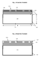
- the Fig. 1 schematically shows a cross section of a basic shape or basic version 100 of a HTS-band conductor.
- An HTS layer 130 must be deposited as an oriented epitaxial layer.
- single-crystalline substrates are required for the deposition of oriented, epitaxial layers, which predetermine the arrangement of the atoms in the layer and thus their crystalline orientation. Since such substrates are very expensive and not available in any size are often cost-effective technical substrates such as the metal sheets, foils or tapes described in this application used as a substrate or as a base material for the production of high-temperature superconductors.
- RABiTS process Rolling Assisted Bi -axed Textured Substrates
- special coating processes for the production of bi-axially oriented buffer layers 120, which may serve as an epitaxial pad for depositing the HTS layer 130.
- An established coating process is the IBAD (Ion Beam Assisted Deposition) process, in which a supporting ion beam is directed onto the substrate surface 110 at a certain angle during deposition. Basic variants of this method are in the EP 0 872 579 A1 and the EP 1 178 129 A1 described.
- the basic form 100 of the HTS-band conductor of Fig. 1 comprises a thin metal foil as the substrate 110, which typically constitutes more than 80% of the total thickness of the basic form 100 of the HTS ribbon conductor.
- Typical substrate materials are alloys of at least two of the elements nickel (Ni), chromium (Cr), iron (Fe), molybdenum (Mo), manganese (Mn), tungsten (W), vanadium (V) etc., such as Ni with Admixtures of 3-10% W, Ni with admixtures of 5-15% Cr, Hastelloy TM C 276, Haynes TM 242, or stainless steels such as SUS TM 310, SUS TM 410, Monel TM or Inconel TM.
- the thickness or height H of the metal substrate 110 is typically in the range of 30 .mu.m-200 .mu.m.
- the width B of the metal substrate 110 includes a range of 3 mm to 100 mm.
- One or more buffer layers 120 are preferably arranged on the metal substrate 110, which inter alia serve for adhesion promotion, as diffusion barriers, and - as explained in the preceding sections - for generating or for transferring a crystalline orientation.
- the smoothed front side 112 of the substrate 100 has an RMS (Route Mean Square) roughness of less than 10 nm. On short scales of a few micrometers, the roughness of the front side 112 of the substrate 110 is preferably less than 1 nm.
- One or mostly several intermediate or buffer layers 120 are deposited on the front side 112.
- the buffer layers 120 are mainly metal oxides such as magnesium oxide (MgO), cerium oxide (CeO 2 ), aluminum oxide (Al 2 O 3 ), yttrium oxide (Y 2 O 3 ), or mixed oxides such as yttrium-stabilized zirconium oxide (YSZ). , Gd 2 Zr 2 O 7 , La 2 Zr 2 O 7 , LaMnO 3 , SrTiO 3 . Occasionally, metal nitrides such as titanium nitride (TiN) are used.
- MgO magnesium oxide
- CeO 2 cerium oxide
- Al 2 O 3 aluminum oxide
- Y 2 O 3 yttrium oxide
- YSZ yttrium-stabilized zirconium oxide
- Gd 2 Zr 2 O 7 La 2 Zr 2 O 7
- LaMnO 3 LaMnO 3
- SrTiO 3 SrTiO 3
- metal nitrides such as titanium nitride (Ti
- the buffer layers 120 both individually and in their sequence as multilayers, constitute good electrical insulators or poor electrical conductors, so that direct electrical current flow between an HTS layer 130 and the metal substrate 110 is prevented.
- the buffer layers 120 usually have a combined thickness of between 100 nm and several microns.
- the actual HTS functional layer 130 follows, which carries the current in the superconducting application and typically has a thickness of 0.5 ⁇ m -10 ⁇ m.
- the HTS layer thickness 130 is in the range of 1.5 microns - 5 microns.
- HTS layers 130 are made of RBa 2 Cu 3 O 7 , where R is yttrium, a rare earth element, or mixtures of at least two of these elements.
- the stoichiometry of the HTS layer 130 may vary within certain limits, typically within ⁇ 10%, of the ideal 1: 2: 3 composition.
- HTS layer 130 An important component of HTS layer 130 is oxygen.
- the dumping of the HTS layer 130 occurs in an environment containing oxygen.
- the deposition of the HTS layer 130 occurs at high temperatures (over 650 ° C). Under these conditions, a thin oxide layer 140 is formed on the exposed edges 116 and the back side 114 of the metallic substrate 110, or in other words, the edges 116 and back 114 of the metal substrate 110 are scaled. Even in the deposition of the buffer layers 120 on the substrate front side 116, insulating material can reach the edges and the back side 114 of the substrate 110 as a result of scattering in the residual gas and cover it with a layer 140.
- the backside 114 can be intentionally coated with a thin oxygen impermeable layer 140 (e.g., MgO) to prevent severe scaling during high temperature processes.
- a thin oxygen impermeable layer 140 e.g., MgO
- these layers have an adverse effect on the contacting of the substrate back 114 and should therefore be completely or at least partially removed before applying a contact layer 150.
- the direct application of a contact layer 150 to the HTS layer 130 and the edges 116 and the back side 114 of the substrate 110 results in a large contact resistance between the contact layer 150 and the metal substrate 110 without removing the oxide layer 140.
- the contact layer 150 is shown in FIG Fig. 2 shown schematically.
- the oxide layer 140 causes the problems discussed in the opening section.
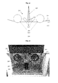
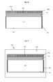
- the Fig. 3 1 schematically shows a section through an exemplary device 300 with the aid of which the oxide layer 140 can be removed from the rear side 114 of the metallic substrate 110.
- an Nd: YVO 4 laser an yttrium-vanadate laser (YVO 4 with neodymium doping) from Rofin is used (Rofin PL E10).
- the Nd: YVO 4 laser emits light with a wavelength of 1064 nm. It has an adjustable pulse repetition frequency of 0-200 kHz at a average power of 10W. The pulse duration is about 10 ns.
- the laser beam 310 of the Nd: YVO 4 laser can, with the aid of a galvo scanner, rasterize the substrate 110 in a programmable form (in the US Pat Fig. 3 not shown).
- the lines 340 symbolize a section through the scanning region in the longitudinal direction of the metal substrate 110.
- the arrow 350 in the Fig. 3 indicates the transport direction of the metal substrate 110.
- the suction device 360 makes it possible to remove the debris of the oxide layer 140 that has been blown away by the laser beam 370 from the rear side 114 of the metal substrate 110.
- the process area in the process chamber 340 can be observed with a camera, such as a CCD (Charge-Coupled Device) camera (in U.S. Pat Fig. 3 Not shown).
- a pilot laser that emits light in the visible region of the spectrum may be used to position the Nd: YVO 4 laser (eg, a He-Ne (helium-neon) laser or a semiconductor laser).
- the Fig. 3a shows a view into an existing real apparatus 350.
- the metal substrate 110 to be processed is guided via the deflection rollers 320 and the entrance slit 330 into the interior of the process chamber 340.
- the suction nozzles 360 are mounted, which suck the material removed by the laser beam 310.
- the laser beam 310 (not visible) is guided from above to the rear side 114 of the metal substrate 110.
- FIG. 12 illustrates the scanning or scanning of the laser beam 310 over a metallic substrate 110 of a HTS ribbon conductor.
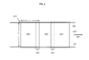
- the Fig. 4 shows a plan view of the back 114 of the metal substrate 110.
- the metal strip 110 moves continuously. This is in the Fig. 4 symbolized by the arrow 450.
- the galvo scanner of the laser system scans the laser beam 310 line by line over a rectangle 430 with the area a ⁇ b.
- the galvo scanner Upon completion of the scan of the rectangle 430, the galvo scanner advances to the next rectangle 430 in the transport direction 450 and scans the laser beam 310 over the next rectangle 430 with the dimensions given above.
- the galvo scanner By choosing an overlap 440 of the individual scan areas of 2 mm, it is ensured that the oxide layer 140 is treated completely from the entire rear side 114 of the metal substrate 110.
- an excimer laser can be used instead of the laser of Fig. 3 .
- An excimer laser has at least two advantages: (a) due to the shorter wavelength (in the ultraviolet wavelength region), a much larger fraction of the laser radiation 310 is absorbed in the oxide layer 140 on the back side 114 of the metal substrate.
- removal of the oxide layer 140 from the back side 114 of the metal substrate 110 should be at a speed of at least 20 m / h.
- the operating parameters of the laser system or the laser parameters were varied while the tape winder was idle, ie, without transporting the metal substrate, and the results were compared visually to get a rough idea of which parameters lead to better results in removing the oxide layer 140.
- the descaling or the removal of the oxide layer from the rear side 114 of the metal substrate 110 is also called cleaning of the metal substrate 110. It has been found that lower pulse repetition rates and low scan speeds (ie, speed of laser beam movement in the rectangle 430) result in better results in ablation of the oxide layer 140.
- the Fig. 3 Only pulse repetition rates of less than 20 kHz provide sufficient pulse energy for visible descaling or cleaning success, ie for visible removal of the oxide layer 140 from the back side 114 of the metal substrate 110.
- the pulse energy increases with decreasing pulse repetition rate, because more energy is left in the active medium of the laser system between two pulses.
- the time between two pulses is 0.1 ms; this time corresponds approximately to the lifetime of the upper state of the laser transition in the active medium of the Nd: YVO 4 laser. Reducing the pulse repetition rate R p below 10 kHz does not result in a higher pulse energy because the spontaneous emission prevents further increase in the energy collected from the pump energy in the active medium.
- the energy of a laser pulse is sufficient to effectively remove the oxide layer 140.
- adjacent laser spots ie, areas of impact of laser pulses on oxide layer 140
- rectangle 430 As a scan area that was in the Fig. 4 shown rectangle 430 selected.
- the rectangle 430 is created by the juxtaposition of lines, which are rastered transversely to the tape longitudinal direction.
- the width of the hatching lines is an input parameter of the laser system Fig. 3 , It should correspond to the diameter of the laser spot (here approx. 75 ⁇ m).
- the entered width of the hatching lines together with their overlap, which is also adjustable, affects the distance between the hatching lines. A smaller spacing of adjacent hatching lines or a larger overlap improves the removal of the oxide layer 140 from the back side 114 of the metal substrate, but limits the achievable belt speed or, more generally, the surface removal rate.
- the achievable belt speed v band is obtained from the scan speed v scan 'of the line length l (corresponding to the width b of the rectangle 430), the width of the line w (ie the diameter of the laser beam 310 when hitting the oxide layer) and the overlap p, wherein the overlap of the hatching line in the longitudinal direction of the metal strip describes.
- this tape speed can not be achieved because in "on-the-fly" mode, ie when scanning rectangles on moving substrate, the distance of adjacent rectangles 430 must be smaller than the width of the individual rectangles, as in Context of Fig. 4 discussed - to ensure a complete coverage of the metal strip 110 by the laser beam 310.
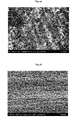
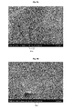
- FIGS. 5a and 5b show the surfaces of substrate backs 114 with different oxide layers 140 in the scanning electron microscope at 20000x magnification.
- this is essentially MgO, which arrives at the rear side 114 during the deposition of the buffer layer 120.
- Fig. 5b it is a scaled (oxidized Hastelloy TM C276 surface, in both cases the oxide layer 140 is very rough.
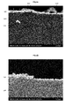
- the Figures 6a and 6b show cross sections through the surfaces of the FIGS. 5a and 5b , Below the MgO oxide layer 140 have in the Fig. 6a By diffusion into the surface 114 of the metal substrate 110 in pores 610 formed, which affect the adhesion of the oxide layer 140 on the metal substrate 110. Also in the Fig. 6b for example, the interface between oxide layer 140 and substrate 110 is characterized by an irregular roughness depth of up to 50 nm. The thickness of oxide layer 140 is in the range of less than one micron.
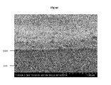
- the Fig. 7a shows a laser-cleaned back side 114 of a metal substrate 110 at low 100-fold magnification in the scanning electron microscope (SEM).
- SEM scanning electron microscope
- the Fig. 7b represents an SEM image with the magnification indicated in the previous section, in the lower part of which the oxide layer 140 is still present (light area), while in the upper part the oxide layer 140 has been largely removed by laser pulses (dark area).
- the transition between oxide-backed back surface 114 and cleaned surface is clearly visible.
- Clearly recognizable is also the characteristic of the cleaning process dot matrix. In the central areas of the laser focus, the oxide layer was completely removed and the metal substrate 110 (dark areas) exposed.
- FIGS. 8a and 8b show at high magnification (20,000 times) the central focus area of a laser pulse on the irradiated back side 114 of a metal substrate 110.
- the MgO layer became the Fig. 5a treated with the laser. It is characterized by the characteristic occurrence of cracks 810 in the surface of the metal substrate 110. The surface was obviously melted down to a shallow depth by the laser bombardment. As the melt solidified and rapidly cooled, stresses created by a shrinkage process relaxed through surface-near cracks 810.
- the Fig. 8b shows the laser-treated surface of the Fig. 5b , Cooling cracks 810 in the surface 810 occasionally occur here.
- the Figures 9 and 9b show at different magnifications cross-sectional preparations of a metal substrate 110 with an oxide layer 140 analogous to the Fig. 6a Near-surface transition region between the scale or oxide layer 140 and the area 930, in which these oxide layers 140 were largely removed by means of laser pulses.
- the Fig. 9a is in the left half of the picture at 20000-fold magnification, the 300 nm to 400 nm thick oxide layer 140 clearly visible.
- the Fig. 9b shows a part of the Fig. 9a with 50000x magnification.
- a molten one Layer 920 which has two cracks 910, which extend from the surface of the remaining oxide layer to the back surface 114 of the metal substrate 110.
- the Fig. 9c shows the laser-treated scale layer analogous to the Fig. 6b at 50000x magnification. Again, a melted surface layer 920 is visible. Unlike the Fig. 6b For example, the interface between the surface view 920 and the substrate 110 is smooth and featureless.
- Some of the most important criteria for assessing the success of the oxide layer removal or for characterizing the cleaning results are the values of the junction resistance between the contact layer 150 and the metal substrate 110 of the HTS ribbon conductor and / or the adhesion of the contact layer applied to the back side 114. In the following, first results of the measurement of the contact resistance will be presented.
- the oxide layer 140 has been removed from the back side 114 of the metal substrate 110.
- the cleaning was carried out at a belt speed of 18 m / h.
- the repeat distance in on-the-fly mode was 10 mm (cf. Fig. 4 ).
- the scan area of the laser beam 310 comprised a 13.5 mm wide and 12 mm long rectangle 430. This ensured that a 2 mm overlap between adjacent rectangles 430 was always maintained.
- the back side 114 of the metal substrate 110 after the removal of the oxide layer 140 is coated with a contact layer 1060 made of silver.
- a contact layer 1060 made of silver.
- other precious metals such as gold and alloys of precious metals can be used for the contact layer.
- the samples were heated to 200 ° C for two hours.
- the Fig. 11 shows a cross section through a substrate back of a HTS-strip conductor, which after the laser treatment with a silver contact layer 1060 of 2.5 .mu.m to 3 .mu.m thickness coated and annealed between 600 - 300 ° C in an oxygen atmosphere for 12 minutes. At this temperature, there is a significant interlocking between the molten surface layer 920 and the silver layer 1060, while the interface with the substrate 110 remains untouched.
- the silver layer 1060 was then removed by means of a silver-etching solution to several approximately 7x5 mm 2 large silver contact surfaces 1060, which are arranged at a distance of about 1 cm, respectively.
- the HTS-Bandleiter Configuration 1200 of the Fig. 12 shows the configuration 1000 of the Fig. 10 after completion of the etching process.
- the silver pads 1260 are used as contacts for the resistance measurements.
- the resistances between the measurement points 1260 on the back side 114 of the metal substrate 110 are measured at different distances along the sample with a Keithley 2700 multimeter in four-point geometry.
- the terminals 1275 serve to impress a defined current.
- the voltage drop between the silver pads 1260 is measured.
- the contacts for the current 1275 and the voltage measurement 1270 are soldered together for each measurement point on a silver contact surface 1260.
- the measurement error for a single measurement is about 100 ⁇ . Four point measurements were therefore needed to eliminate the line resistances. For comparison, two-point measurements were also carried out. These result in higher values by approx. 200 m ⁇ , which roughly corresponds to the line resistance.
- the four point measured resistance between the silver pads 1260 is the sum of the contact resistances between the silver pads 1260 and the metal substrate 110 and the resistance of the metal substrate 110.
- the resistance of the metal substrate increases linearly with the distance I of the measurement points, i. the distance of the silver pads 1260.
- the transition resistances should be constant with a constant size of the contacts and homogeneous back surface 114.
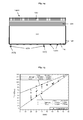
- FIG. 13 A typical measurement result after removing the oxide layer 140 is in Fig. 13 shown.
- the central, cleaned surfaces of the individual pulses begin to overlap and the measured resistances are largely independent of scan parameters such as the scan speed, the line spacing and the overlap of the pulses.
- the resistance increases linearly as a function of distance I.
- the intersection of the straight lines with the y-axis, which corresponds to the sum of the contact resistances, is reproducibly close to the origin (o m ⁇ ), within a defect width of less than 1.6 m ⁇ ⁇ cm 2 .
- a silver layer was applied to an untreated oxide layer 140 and patterned as described above.
- the Fig. 14 illustrates this configuration 1400.
- the resistance measurements on uncleaned substrates are in Fig. 15 shown.
- the different symbols designate measurement series between different samples and contact surfaces and scatter considerably, so that there is no clearly linear dependence on the distance. That is, the contact resistances under the individual contact surfaces deviate greatly from one another and scatter by up to 40 m ⁇ . Accordingly, no reproducible contact resistances between the metal substrate 110 and the silver layer 1060 having a specific resistance ⁇ 1 m ⁇ ⁇ cm 2 can be achieved without the inventive cleaning and contacting method.
- the noise component of the resistive measurement is evaluated with a spectrum analyzer, the 1 / f noise of untreated samples is at least an order of magnitude higher than for samples whose oxide layer has been removed with a laser.
- the Fig. 16 shows the basic form 100 of the HTS-band conductor of Fig. 1 after removing the oxide layer 140 from the back side 114 of the metal substrate 110 and applying a contact layer 1680 that connects the HTS layer 130 to the metal substrate 110.
- silver or silver alloys eg with gold (Au) and / or copper (Cu) fractions
- Cu copper
- the thickness of the contact layer 1680 is preferably in the range of 0.3 .mu.m-3 .mu.m in order to ensure a closed covering of the edges and good solderability of the HTS strip conductor 1600.
- the total thickness of the coatings 120, 30 and 140 or the HTS layer sequence is typically in the range of 3 .mu.m-10 .mu.m and is thus small compared to the thickness of the metal substrate 110.
- the removal of the oxide layer 140 from the back side 114 of the metal substrate with a Nd: YVO 4 laser from Rofin reduces the contact resistances between the contact layer 1680, in the example of FIG Fig. 16 a silver layer and the metal substrate 110, in the example of FIG Fig. 16 a Hastelloy substrate of about one order of magnitude, from a maximum of 40 milliohms to less than 1 milliohms.
- the performed removal of the oxide layer 140 from the back side 114 of the metal substrate has no influence on the critical current densities of the HTS layer 120.
- adhesion test attempts were also carried out on the contact layers 1680 to determine the adhesion of the contact layers 1680 to the metal substrate 110.
- Scotch tape test peel-on tape applied to contact layer 1680 and then jerked off the side readily survived a silver contact layer 1680 made in accordance with the present invention applied to a laser-treated back side 114 of the metal substrate.
- a stamping test was carried out to quantify the adhesion of the contact layer 1680 on the metal substrate 110.
- the sample was according to Fig. 16 first glued flat with the front down on a flat surface.
- the back of the substrate 114 was covered with a metal mask with a round hole and pressed onto the substrate.
- a round metal cylinder (stamp) with a diameter of 6 mm was centered and glued plane-parallel with its end face onto the silver layer 1480 affixed to the rear side 114 of the metal substrate 140 (adhesive: two-component epoxy resin adhesive Araldit 2011 TM or UHU 300 Plus endfest TM) , The punch was pulled up with a hydraulic tensile tester perpendicular to the substrate surface until it was torn off. For the adhesive strength of the silver layer on the laser-cleaned substrate back 114, values ⁇ 4 MPa were measured. It should be noted that at loads> 10 MPa, the adhesives used to fail. Thus, it can be noted that contact layers 1680 applied to the back side 114 of a metal substrate 110, whose oxide layer 140 was previously removed by means of a laser, typically have bond strengths> 1 MPa.
- the 1600 configuration of a HTS ribbon conductor must be reinforced with additional layers or sheaths for electrical or mechanical stabilization. This can e.g. by electrodepositing copper or other metals or by laminating with other metal foils, e.g. Copper, brass or stainless steel happen.
- the chart 1700 of the Fig. 17 shows the HTS-Bandleiter the Fig. 15 after attaching a stabilizing layer 1790 of copper.
- a stabilization layer 1790 is necessary to protect the HTS layer 130 from short-term overload.
- the thickness of this stabilization layer 1790 is typically 10 ⁇ m-100 ⁇ m, preferably 20 ⁇ m-50 ⁇ m, and is thus already in the region of the substrate thickness.
- the HTS ribbon conductor now appears like a metal foil, its surface properties corresponding to the material of the stabilization layer 1790.
- a layer of solder may optionally be applied in addition to the stabilized strip conductor in whole or in part, a layer of solder. This can be done either by electrodeposition, by a solder wave or a dip in molten solder. If the application of liquid solder, it is advisable in advance to treat the surfaces of the stabilizing layer 1790 with a flux that improves the wetting of the surfaces. To prevent degradation of the HTS tape conductor, the melting temperature of the solder should not exceed 250 ° C. Preferably, it is below 200 ° C.
- the HTS tape conductor can be wrapped with a thin plastic film or with paper. Furthermore, it is possible to laminate the strip conductor on both sides with a thermoplastic film, wherein supernatants must be beaded or fused at the edges.
- Another method for protecting a strip conductor is the application of a lacquer layer. Since the HTS strip conductor is cooled down to ⁇ 93 K during operation, the material of the insulation must not become brittle and should be adapted to the thermal expansion of the strip conductor. Common materials include polyimide (PI), also known by the tradename Kapton TM or polyetheretherketone (PEEK).
- a solution of polyamidocarboxylic acid which is e.g. by immersion in a dipping bath, spraying or other common methods of enamel wire production on the HTS band conductor applies.
- the viscosity should be limited by the proportion of solvent, e.g. N-methyl-2-pyrrolidone (NMP) or dimethylformamide, adjusted to ensure complete edge coverage.
- NMP N-methyl-2-pyrrolidone
- the paint layer can also be formed by a scraper. Also voids or bubbles can be removed.
- the coated tape passes through a hot zone e.g. in a tube furnace in which the paint reacts to polyimide and crosslinks.
- the temperature for crosslinking is above 250 ° C, preferably between 300 ° C and 400 ° C.
- Hastelloy TM C276 substrate 12 mm wide and 100 ⁇ m thick becomes at 30 ° counter to the direction of incidence at room temperature and 10 -4 mbar oxygen residual gas pressure by electron beam evaporation with a 3 ⁇ m thick MgO-ISD buffer layer coated.
- MgO-ISD buffer layer coated by scattering in the residual gas Also passes a small amount of MgO on the unpolished substrate back, where it forms an approximately 200 nm thick, insulating protective layer.
- a 300 nm thick MgO cover layer and then a 2-3 ⁇ m thick HTS layer of GdBa 2 Cu 3 O 7 are then applied to the MgO-ISD buffer layer at 720 ° C.
- the substrate backside is treated with the Rofin Nd-YAG laser system described above with a pulse frequency of 20 kHz and a scan speed of 1000 mm / s.
- the band conductor is coated in vacuo by evaporation with a 2 micron thick silver layer around and then pulled in a pure oxygen atmosphere at a speed of 20 m / h through a 4 m long tube furnace with a temperature gradient of 600 ° C to 300 ° C.
- the observed contact resistance between the silver layer and the substrate was below 10 -3 ⁇ ⁇ cm 2 and the peel strength of the silver layer was more than 1 MPa.
- Hastelloy TM C276 substrate 12 mm wide and 60 ⁇ m thick was first provided with texturing buffer layers by the IBAD process and then with a layer of GdBa 2 Cu 3 O 7 at a temperature of 750 ° C coated. Due to the high temperature and the high oxygen partial pressure during the coating, an approximately 200 nm thick scale layer was formed on the back of the substrate.
- the substrate backside was treated with the laser as in Example 1 and coated and annealed analogously to Example 1 with silver. Even in this case, significantly improved adhesion and contact resistance could be demonstrated compared to the untreated back.
Abstract
Die Erfindung betrifft ein Verfahren zum Herstellen eines Hochtemperatur-Supraleiters (1700) mit den Schritten: (a)Aufbringen zumindest einer Hochtemperatur-Supraleiterschicht (130) auf zumindest eine nichtleitende Schicht (120), die auf einer Vorderseite eines metallischen Substrats (110) angeordnet ist; (b) Zumindest teilweises Entfernen einer Isolatorschicht (140) von einer Rückseite (114) des metallischen Substrats (110); und (c) Aufbringen einer elektrisch leitenden Kontaktschicht (1680) auf die Rückseite (114) des metallischen Substrats (110), wobei die Kontaktschicht (1680) elektrisch mit der Hochtemperatur-Supraleiterschicht (130) verbunden ist.The invention relates to a method for producing a high temperature superconductor (1700) comprising the steps of: (a) applying at least one high temperature superconductor layer (130) to at least one nonconductive layer (120) disposed on a front side of a metallic substrate (110) is; (b) at least partially removing an insulator layer (140) from a backside (114) of the metallic substrate (110); and (c) applying an electrically conductive contact layer (1680) to the back surface (114) of the metallic substrate (110), wherein the contact layer (1680) is electrically connected to the high temperature superconductor layer (130).
Description
Die vorliegende Erfindung betrifft ein Verfahren und eine Vorrichtung zum Herstellen eines Hochtemperatur-Supraleiters.The present invention relates to a method and an apparatus for producing a high-temperature superconductor.
Hochtemperatur-Supraleiter stellen in der Elektro- und Energietechnik ein Standardleitermaterial dar, aus dem Leitungen, Kabel oder Windungen und Spulen hergestellt werden. HTS-Bandleiter ersetzen in diesen Anwendungen Kupferdraht, da sie um ein Vielfaches höhere elektrische Ströme transportieren können. Diese hohen Ströme würden im Kupfer zu hohen ohmschen Verlusten führen. Mit dem Einsatz von Supraleitern können diese Verluste verringert und eine erheblich kompaktere Bauweise realisiert werden.High-temperature superconductors represent a standard conductor material in electrical engineering and energy technology, from which cables, cables or windings and coils are produced. HTS tape conductors replace copper wire in these applications because they can carry many times higher electrical currents. These high currents would lead to high ohmic losses in the copper. With the use of superconductors, these losses can be reduced and a significantly more compact design can be realized.
Weiterhin können auch Komponenten, bei denen bereits heute metallische Supraleiter statt Kupferleiter eingesetzt werden, z.B. Magnetresonanztomographen oder starke Elektromagnete, verbessert werden. Hochtemperatur-Supraleiter erlauben eine deutlich höhere Betriebstemperatur und halten höheren Magnetfeldern stand. Zudem führt die resultierende Verringerung des Kühlaufwandes zu einem einfacheren Aufbau und einer Verbesserung des Wirkungsgrades.Furthermore, components in which metallic superconductors are already used instead of copper conductors, e.g. Magnetic resonance imaging or strong electromagnets, to be improved. High-temperature superconductors allow a much higher operating temperature and withstand higher magnetic fields. In addition, the resulting reduction in cooling costs leads to a simpler structure and an improvement in the efficiency.
Die Herstellung von HTS-Bandleitern erfolgt durch kontinuierliche, physikalische oder chemische Beschichtungsverfahren von Rolle zu Rolle. Ein flexibles, metallisches Substratband wird dabei von einer Vorratsrolle abgespult, durch Beschichtungs- und Prozesszonen geführt und auf der anderen Seite wieder auf eine Vorratsspule aufgewickelt.The production of HTS strip conductors is carried out by continuous, physical or chemical coating processes from roll to roll. A flexible, metallic substrate strip is unwound from a supply roll, passed through coating and processing zones and wound on the other side again on a supply reel.
Die Beschichtung mit Pufferschichten und HTS-Schichten erfolgt normalerweise einseitig, d.h. auf einer polierten oder geglätteten Hauptfläche des Substratbands. Die Pufferschichten stellen einzeln oder in ihrer Abfolge als Multilagen gute elektrische Isolatoren, bzw. schlechte elektrische Leiter dar, so dass ein direkter Stromfluss zwischen der HTS-Schicht und dem Metallsubstrat nicht möglich ist. Im Einsatz als elektrischer Leiter können sich also die HTS-Schicht und das Metallsubstrat lokal auf unterschiedlichem elektrischem Potenzial befinden. Da die Pufferschichten nur sehr dünn sind (im Bereich einiger Mikrometer), können bereits bei einigen Volt Potenzialdifferenz zwischen der HTS-Schicht und dem Metallsubstrat, elektrische Felder von einigen 106 V/m über der oder den Pufferschicht(en) entstehen, so dass es zum dielektrischen Durchbruch kommen kann, der mit der lokalen Zerstörung der Schichten und damit des HTS-Bandleiters einhergeht.The coating with buffer layers and HTS layers usually takes place on one side, ie on a polished or smoothed main surface of the substrate strip. The buffer layers individually or in their sequence as multilayers constitute good electrical insulators or poor electrical conductors, so that direct current flow between the HTS layer and the metal substrate is not possible. When used as an electrical conductor, therefore, the HTS layer and the metal substrate can be located locally at different electrical potential. Since the buffer layers are only very thin (in the range of a few microns), even at a few volts potential difference between the HTS layer and the metal substrate, electric fields of some 10 6 V / m above the buffer layer (s) can occur, so that It may come to the dielectric breakthrough, which is associated with the local destruction of the layers and thus the HTS-band conductor.
Es ist deshalb zwingend erforderlich, einen separaten und möglichst niederohmigen elektrischen Kontakt zwischen der HTS-Schicht und dem Metallsubstrat herzustellen. Dies wurde insbesondere dort erkannt, wo der HTS-Bandleiter explizit zum Schalten zwischen dem supraleitenden und dem normalleitenden Zustand eingesetzt wird. So beschreibt die
Üblicherweise geschieht die Kontaktierung der HTS-Schicht und dem Substrat des HTS-Bandleiters durch eine Schicht aus einem guten metallischen Leiter, der auf die HTS-Schicht und die offen liegenden Seitenflächen und die Rückseite des Bandleiters aufgebracht wird. Diese Schicht stellt gleichzeitig die elektrische Kontaktschicht zur HTS-Schicht dar, durch die elektrischer Strom in die HTS-Schicht ein- und ausgekoppelt wird. Als unmittelbare Kontaktschicht dienen normalerweise Edelmetalle wie Ag, Au bzw. Legierungen dieser Elemente, die an der Grenzfläche zum Supraleiter nicht oxidieren. Die Beschichtung kann durch chemische und physikalische Verfahren erfolgen. Normalerweise wird die Schicht beidseitig bzw. rundherum im Vakuum auf den HTS-Bandleiter aufgedampft oder gesputtert.Usually, the contacting of the HTS layer and the substrate of the HTS ribbon conductor is done by a layer of a good metallic conductor, which is applied to the HTS layer and the exposed side surfaces and the back of the stripline. This layer simultaneously provides the electrical contact layer to the HTS layer is, by the electric current in the HTS layer is coupled and decoupled. Precious contact layers are normally noble metals such as Ag, Au or alloys of these elements which do not oxidize at the interface to the superconductor. The coating can be done by chemical and physical methods. Normally, the layer is vapor-deposited or sputtered on both sides or all around in a vacuum onto the HTS ribbon conductor.
Während sich dadurch ein akzeptabler elektrischer Kontakt zur HTS-Schicht herstellen lässt, bereitet der Kontakt zum Metallsubstrat jedoch Probleme. Die Depositionsprozesse der HTS-Schichten und teilweise auch der Pufferschichten finden nämlich typischerweise bei hohen Temperaturen > 600 °C und unter Sauerstoffeinwirkung statt, d.h. in einer oxidierenden Atmosphäre. Durch diese Hochtemperaturprozesse oxidieren, bzw. verzundern die offen liegenden Kanten und die Rückseite des Metallsubstrats. Es bilden sich auf der Oberfläche zumindest in Teilbereichen des Metallsubstrats elektrisch schlecht oder nicht leitende Metalloxidschichten, u.a. aus NiO, Cr2O3, Fe2O3 etc.While this provides acceptable electrical contact to the HTS layer, contact with the metal substrate presents problems. Namely, the deposition processes of the HTS layers and partially also of the buffer layers typically take place at high temperatures> 600 ° C. and under the action of oxygen, ie in an oxidizing atmosphere. As a result of these high-temperature processes, the edges which are exposed and the back side of the metal substrate become oxidized. Electrically poorly or non-conducting metal oxide layers are formed on the surface, at least in partial regions of the metal substrate, inter alia of NiO, Cr 2 O 3 , Fe 2 O 3, etc.
Die leitfähige Kontaktschicht wird zwar weiterhin häufig noch mit Kupfer oder anderen Metallen verstärkt, z.B. durch galvanisches Aufdicken oder das Auflöten von einer Metallfolie, dies ändert aber nichts am schlechten Grenzflächenkontakt zwischen der Edelmetallschicht und dem Metallsubstrat des HTS-Bandleiters und dem damit verbundenen hohen Übergangswiderstand.Although the conductive contact layer is still often reinforced with copper or other metals, e.g. However, this does not change the poor interfacial contact between the noble metal layer and the metal substrate of the HTS ribbon conductor and the associated high contact resistance.
Durch seitliches Schleifen, Besäumen oder Längsteilen des Bandleiters, d.h. durch Aufschneiden in schmalere Leiter vor der rundum-Beschichtung mit Silber, wie in
Zudem wird der HTS-Bandleiter nach der Abscheidung der Silberschicht in Sauerstoffatmosphäre bei Temperaturen > 300 °C ausgelagert. Vorzugsweise werden Temperaturen > 500 °C angewandt. Dadurch wird zum einen durch Diffusion von Silber in die oberflächennahe Oxidschicht eine Verbesserung der Haftung und des Kontakts erreicht, zum anderen diffundiert Sauerstoff durch die Silberschicht in die HTS-Schicht, so dass diese mit Sauerstoff beladen wird und sich dadurch die supraleitende, orthorhombische Phase ausbildet.In addition, after deposition of the silver layer in an oxygen atmosphere, the HTS strip conductor is removed at temperatures> 300 ° C. Preferably Temperatures> 500 ° C are used. On the one hand, this improves the adhesion and the contact by diffusion of silver into the near-surface oxide layer and, on the other hand, oxygen diffuses through the silver layer into the HTS layer, so that it is charged with oxygen and thereby forms the superconducting, orthorhombic phase ,
Das Eindiffundieren von Silber in die Zunderschicht auf der Substratrückseite kann zu punktuellen Kontakten und einer leichten Verbesserung des elektrischen Kontakts zwischen der Silberschicht und dem Metallsubstrat führen. Damit kann jedoch keine zuverlässige, niederohmige Verbindung hergestellt werden. Gleiches gilt für den Kontakt über die sehr schmalen Kanten des Substrats wie in
Eine weitere Gefahr der Zunderschicht zwischen Substratrückseite und Metallisierung besteht in der Beeinträchtigung der mechanischen Haftung. Da die Struktur der Oxidschicht im Wesentlichen amorph und porös ist, stellt sie bei mechanischer Belastung eine Sollbruchstelle dar und kann zur Delamination der Metallisierung von der Substratrückseite führen. Solche mechanischen Belastungen treten u.a. durch unterschiedliche thermische Ausdehnungen des Substrats und der Metallschicht auf (Bimetalleffekt) oder in gewickelten Magnetspulen infolge des Vergusses, der thermischen Ausdehnung und der magnetische Kräfte.Another danger of the scale layer between substrate back and metallization is the impairment of mechanical adhesion. Since the structure of the oxide layer is substantially amorphous and porous, it represents a predetermined breaking point under mechanical stress and can lead to the delamination of the metallization from the back of the substrate. Such mechanical stresses occur u.a. by different thermal expansions of the substrate and the metal layer on (bi-metal effect) or in wound magnetic coils due to the potting, the thermal expansion and the magnetic forces.
Das Entfernen einer Zunderschicht, die während einer Warmbehandlung eines Metalls entstanden ist, ist schon seit langer Zeit bekannt. Zum Entzundern von Metallen werden diese häufig in ein Säurebad getaucht bzw. gebeizt. Für einen HTS-Bandleiter scheidet dieser Prozess aufgrund der empfindlichen HTS- und Pufferschichten aus.The removal of a scale layer created during a heat treatment of a metal has been known for a long time. For descaling metals, these are often dipped in an acid bath or pickled. For a HTS ribbon conductor, this process is eliminated because of the sensitive HTS and buffer layers.
Ferner ist es ebenfalls bereits bekannt, Laserstrahlung zum Entfernen einer Oxidschicht von einer Metalloberfläche zu einzusetzen. So beschreibt beispielsweise die
Keines dieser Dokumente berücksichtigt jedoch, dass ein Metallband mit einer Oxidschicht auf seiner Rückseite auf seiner Vorderseite mehrere empfindliche Funktionsschichten aufweist, die durch den Prozess des Entzunderns nicht beschädigt werden dürfen. Beispiele möglicher Beschädigungs- bzw. Zerstörungsquellen von Funktionsschichten sind deren Überhitzung bzw. die Einwirkung mechanischer Schockwellen.However, none of these documents takes into account that a metal tape with an oxide layer on its back side has on its front side several sensitive functional layers which must not be damaged by the descaling process. Examples of possible damage or destruction sources of functional layers are their overheating or the action of mechanical shock waves.
Der vorliegenden Erfindung liegt daher das Problem zu Grunde, ein Verfahren und eine Vorrichtung zum Herstellen eines Hochtemperatur-Supraleiters anzugeben, dessen Kontaktschicht einen niedrigen Übergangswiderstand zum Substrat des Hochtemperatur-Supraleiters aufweist.The present invention is therefore based on the problem to provide a method and an apparatus for producing a high-temperature superconductor whose contact layer has a low contact resistance to the substrate of the high-temperature superconductor.
Gemäß einem Ausführungsbeispiel der vorliegenden Erfindung wird dieses Problem durch ein Verfahren nach Anspruch 1 gelöst. In einer Ausführungsform weist das Verfahren zum Herstellen eines Hochtemperatur-Supraleiters die folgenden Schritte auf: (a) Aufbringen zumindest einer Hochtemperatur-Supraleiterschicht auf zumindest eine Pufferschicht, die auf einer Vorderseite eines metallischen Substrats angeordnet ist; (b) Zumindest teilweises Entfernen einer Isolatorschicht von einer Rückseite des metallischen Substrats; und (c) Aufbringen einer elektrisch leitenden Kontaktschicht auf die Rückseite des metallischen Substrats, wobei die Kontaktschicht elektrisch mit der Hochtemperatur-Supraleiterschicht verbunden ist.According to one embodiment of the present invention, this problem is solved by a method according to claim 1. In an embodiment, the method of manufacturing a high temperature superconductor comprises the steps of: (a) applying at least one high temperature superconductor layer to at least one buffer layer disposed on a front surface of a metallic substrate is; (b) at least partially removing an insulator layer from a backside of the metallic substrate; and (c) applying an electrically conductive contact layer to the back surface of the metallic substrate, wherein the contact layer is electrically connected to the high temperature superconductor layer.
In dieser Anmeldung wird eine Isolatorschicht als eine Schicht definiert, die einen größeren Widerstand als das darunterliegend metallische Substrat aufweist. Äquivalent zu dieser Definition weist eine Isolatorschicht in dieser Anmeldung eine spezifische Leitfähigkeit auf, die geringer als die des metallischen Substrats ist. Beispiele derartiger Isolatorschichten sind dünne Oxid- und/oder Nitridschichten. Ferner, kann beispielsweise eine Isolatorschicht in Form einer Oxidschicht neben einem Metall und Sauerstoff geringe Anteile weiterer Elemente enthalten.In this application, an insulator layer is defined as a layer having a greater resistance than the underlying metallic substrate. Equivalent to this definition, an insulator layer in this application has a specific conductivity lower than that of the metallic substrate. Examples of such insulator layers are thin oxide and / or nitride layers. Furthermore, for example, an insulator layer in the form of an oxide layer may contain small amounts of further elements in addition to a metal and oxygen.
Ein erfindungsgemäßes Verfahren ermöglicht es, eine Kontaktschicht auf der Rückseite des Substrats eines Hochtemperatur-Supraleiters (HTS) zu erzeugen, die einen deutlich verbesserten Kraftschluss im Vergleich zum Anbringen einer Kontaktschicht auf eine Isolatorschicht des Substrats aufweist. Damit verringert ein erfindungsgemäßes Aufbringen der Kontaktschicht auf das metallische Substrat eines HTS eine Beschädigung der Kontaktschicht beispielsweise durch deren Delamination während des weiteren Prozessierens oder des Einsatzes des HTS.An inventive method makes it possible to produce a contact layer on the back of the substrate of a high-temperature superconductor (HTS), which has a significantly improved adhesion as compared to attaching a contact layer to an insulator layer of the substrate. Thus, an inventive application of the contact layer on the metallic substrate of an HTS reduces damage to the contact layer, for example by their delamination during further processing or the use of the HTS.
Ferner erlaubt ein erfindungsgemäßes Verfahren das Erzeugen eines zuverlässigen elektrischen Kontakts zwischen der HTS-Schicht und dem zugehörigen Substrat mit einem sehr geringen Übergangswiderstand. Dadurch wird verhindert, dass zwischen der HTS-Schicht und dem metallischen Substrat Potentialdifferenzen auftreten können, deren elektrische Felder die elektrisch nicht oder schlecht leitenden Pufferschicht(en) und /oder die HTS-Schicht und damit den Hochtemperatur-Supraleiter zerstören. Ein nach einem erfindungsgemäßen Verfahren hergestellter HTS kann somit zum reproduzierbaren Schalten zwischen dem supraleitenden und normalleitenden Zustand eingesetzt werden.Furthermore, a method according to the invention allows the generation of a reliable electrical contact between the HTS layer and the associated substrate with a very low contact resistance. This prevents potential differences between the HTS layer and the metallic substrate from occurring whose electric fields destroy the electrically or poorly conducting buffer layer (s) and / or the HTS layer and thus the high-temperature superconductor. An HTS produced by a method according to the invention can thus be used for reproducible switching between the superconducting and normal conducting state.
In einem weiteren Aspekt wird der Schritt b. unter Verwendung eines Lasers durchgeführt, dessen Strahl auf die Isolatorschicht auf der Rückseite des metallischen Substrats gerichtet ist.In another aspect, step b. performed using a laser whose beam is directed to the insulator layer on the back of the metallic substrate.
Der Einsatz eines Lasers zum Entfernen einer Zunderschicht hat den Vorteil, dass dessen Betriebsparameter an die zu entfernende Isolatorschicht und / oder an das darunter liegende Substrat des HTS angepasst werden können. Dies ermöglicht ein Entfernen der Isolatorschicht von der Rückseite des Substrats, ohne die empfindlichen Funktionsschichten auf der Substratvorderseite, d.h. die Zwischen- oder Pufferschicht(en) und die HTS-Schicht zu beschädigen.The use of a laser for removing a scale layer has the advantage that its operating parameters can be adapted to the insulator layer to be removed and / or to the underlying substrate of the HTS. This allows removal of the insulator layer from the back of the substrate without the sensitive functional layers on the substrate front, i. damage the intermediate or buffer layer (s) and the HTS layer.
Gemäß einem anderen Aspekt ist der Laser ausgebildet, Laserpulse mit Pulsdauern kleiner 100 ns, vorzugsweise kleiner 10 ns, mehr bevorzugt kleiner 1 ns, und am meisten bevorzugt kleiner 10 ps zu erzeugen.In another aspect, the laser is configured to generate laser pulses having pulse durations less than 100 ns, preferably less than 10 ns, more preferably less than 1 ns, and most preferably less than 10 ps.
Nach einem weiteren Aspekt weist der Strahldurchmesser des Laserstrahls beim Auftreffen auf die Isolatorschicht einen Durchmesser größer 10 µm, bevorzugt größer 50 µm auf.According to a further aspect, the beam diameter of the laser beam when hitting the insulator layer has a diameter greater than 10 microns, preferably greater than 50 microns.
In einem vorteilhaften Aspekt ist die Leistungsdichte des Laserstrahls beim Auftreffen auf die Isolatorschicht größer als 100 MW·cm-2, bevorzugt großer größer als 300 MW·cm-2, und mehr bevorzugt größer als 1 GW·cm-2.In an advantageous aspect, the power density of the laser beam when hitting the insulator layer is greater than 100 MW · cm -2 , preferably greater than 300 MW · cm -2 , and more preferably greater than 1 GW · cm -2 .
Kurze energiereiche Laserpulse deponieren eine große Menge Energie in extrem kurzer Zeit in einer dünnen Oberflächenschicht, beispielsweise einer Isolatorschicht und heizen diese lokal oder selektiv sehr schnell auf hohe Temperaturen auf. Das erhitzte Material dehnt sich lokal sehr schnell aus und wird damit vom Untergrund, d.h. von der Rückseite des Metallsubstrats weggesprengt oder sogar verdampft.Short high-energy laser pulses deposit a large amount of energy in a very short time in a thin surface layer, for example an insulator layer, and heat it locally or selectively very quickly to high temperatures. The heated material expands locally very quickly and is thus blown away from the substrate, ie from the back of the metal substrate or even evaporated.
Nach einem weiteren günstigen Aspekt liegt die Wellenlänge des Lasers im nahen ultravioletten Bereich, im sichtbaren Bereich oder im nahen infraroten Bereich zwischen 150 nm - 2000 nm, bevorzugt zwischen 200 nm - 1200 nm.According to another advantageous aspect, the wavelength of the laser is in the near ultraviolet range, in the visible range or in the near infrared range between 150 nm - 2000 nm, preferably between 200 nm - 1200 nm.
Die Wellenlänge und die Pulsdauer des Laserstrahls werden so gewählt, dass die Energie der Laserpulse vorwiegend in oder unmittelbar unter der zu entfernenden Isolatorschicht absorbiert wird. Dadurch wird sichergestellt, dass sich das metallische Substrat in seinem Inneren nicht signifikant aufheizt. Je kürzer die Wellenlänge der Laserstrahlung ist, desto geringer ist die Eindringtiefe der elektromagnetischen Strahlung in eine Isolatorschicht, insbesondere in eine Oxidschicht. Dies bedeutet, dass mit geringer werdender Wellenlänge der Anteil der Energie der Laserpulse, der in einer dünnen Isolatorschicht deponiert wird, zunimmt. Damit ermöglicht kurzwellige Laserstrahlung das Verwenden von hohen Leistungsdichten und damit einhergehend großen Abtragraten ohne die Funktionsschichten auf der Vorderseite des HTS-Substrats signifikant thermisch zu belasten.The wavelength and pulse duration of the laser beam are selected so that the energy of the laser pulses is absorbed predominantly in or immediately below the insulator layer to be removed. This ensures that the metallic substrate does not heat up significantly in its interior. The shorter the wavelength of the laser radiation, the lower the penetration depth of the electromagnetic radiation into an insulator layer, in particular into an oxide layer. This means that with decreasing wavelength, the proportion of the energy of the laser pulses, which is deposited in a thin insulator layer, increases. In this way, short-wave laser radiation enables the use of high power densities and concomitantly high removal rates without significantly thermally loading the functional layers on the front side of the HTS substrate.
Ferner kann durch eine entsprechende Wahl der Wellenlänge und der Pulsdauern das Entstehen von Schockwellen in dem metallischen HTS-Substrat verhindert werden, die die auf der Vorderseite des Substrats angebrachten Pufferschicht(en) und/oder die HTS-Schicht beschädigen oder zerstören könnten.Further, by appropriate choice of wavelength and pulse durations, the formation of shockwaves in the metallic HTS substrate that could damage or destroy the buffer layer (s) and / or the HTS layer attached to the front of the substrate can be prevented.
Der Abtrag der Isolatorschicht erfolgt vorzugsweise durch lokale Erwärmung nur der Isolatorschicht, wodurch das Material explosionsartig verdampft und zusätzlich weiteres Material in dessen Nähe wegsprengt. Alternativ kann die Laserstrahlung auch mit einer dünnen Oberflächenschicht des metallischen Substrats wechselwirken, die dadurch in dünner Schicht aufschmilzt und verdampft. In diesem Fall wird das verdampfende Metall die darüber liegende Isolatorschicht wegsprengen. In beiden Fällen liegt die Pulsenergiedichte über der Verdampfungsschwelle (Zerstörungsschwelle) für das jeweilige Material.The removal of the insulator layer is preferably carried out by local heating only the insulator layer, whereby the material evaporates explosively and additionally wegsprengt further material in its vicinity. Alternatively, the laser radiation can also interact with a thin surface layer of the metallic substrate, which thereby melts and evaporates in a thin layer. In this case, the evaporating metal will blast away the overlying insulator layer. In both cases, the pulse energy density is above the evaporation threshold (destruction threshold) for the respective material.
In einem vorteilhaften Aspekt weisen benachbarte Pulse eine laterale Überlappung ihrer Auftreffflächen auf der Isolatorschicht von 0 % - 50 %, bevorzugt 0 % - 30 %, und am meisten bevorzugt 10 % - 20 % auf.In an advantageous aspect, adjacent pulses have a lateral overlap of their impact surfaces on the insulator layer of 0% -50%, preferably 0% -30%, and most preferably 10% -20%.
Wenn wirtschaftliche Zwänge außer Betracht gelassen werden können, kann eine Isolatorschicht mit Hilfe von Laserpulsen im Wesentlichen vollständig entfernt werden. In einem wirtschaftlichen Umfeld ist jedoch die Geschwindigkeit, mit der eine Isolatorschicht von dem Substrat eines HTS entfernt werden kann, die entscheidende Größe. Ein erfindungsgemäßes Verfahren kann deshalb dahingehend optimiert werden, dass einerseits nach dem Entfernen der Isolatorschicht eine Kontaktschicht mit geringem Übergangswiderstand auf das Substrat abgeschieden werden kann und andererseits die Flächenrate, mit der die Isolatorschicht entfernt wird, möglichst hoch wird. In diesem Spannungsfeld kann es sinnvoll sein, geringe Teile der Isolatorschicht beispielsweise zwischen den einzelnen Laserpulsen auf der Rückseite des metallischen Substrats zu belassen, solange dadurch die Funktion der Kontaktschicht nicht beeinträchtigt wird.When economic constraints can be disregarded, an insulator layer can be substantially completely removed by means of laser pulses. However, in an economic environment, the speed at which an insulator layer can be removed from the substrate of an HTS is the critical size. An inventive method can therefore be optimized so that on the one hand after removal of the insulator layer, a contact layer with low contact resistance can be deposited on the substrate and on the other hand, the surface rate at which the insulator layer is removed as high as possible. In this voltage field, it may be useful to leave small parts of the insulator layer, for example between the individual laser pulses on the back of the metallic substrate, as long as the function of the contact layer is not affected.
Der Begriff "im Wesentlichen" bedeutet hier wie an anderen Stellen dieser Beschreibung, die Angabe einer Größe innerhalb üblicher Fehlergrenzen.As used elsewhere in this specification, the term "substantially" means the indication of a quantity within common limits of error.
Gemäß noch einem anderen Aspekt ist ein zeitlicher Abstand zwischen dem Auftreffen von zwei Pulsen an einer gleichen Stelle der Isolatorschicht größer als 1 µs, bevorzugt größer als 50 µs, und am meisten bevorzugt größer 100 µs.In yet another aspect, a time interval between the arrival of two pulses at a same location of the insulator layer is greater than 1 μs, preferably greater than 50 μs, and most preferably greater than 100 μs.
Durch den zeitlichen Abstand wird sichergestellt, dass sich das Substrat nicht mehr als notwendig lokal erwärmt. Dadurch kann verhindert werden, dass thermische Spannungen zwischen dem metallischen Substrat und den Funktionsschichten so groß werden, dass sie den HTS beschädigen können.The time interval ensures that the substrate does not heat up more than necessary locally. As a result, it is possible to prevent thermal stresses between the metallic substrate and the functional layers from becoming so great that they can damage the HTS.
Nach einem weiteren vorteilhaften Aspekt weist ein nach dem Schritt b. auf der Rückseite des metallischen Substrats verbleibender Rest der Isolatorschicht eine Struktur auf, die im Wesentlichen durch Betriebsparameter des Lasers bestimmt wird.According to a further advantageous aspect, an after step b. On the back of the metallic substrate remaining remnant of the insulator layer on a structure which is determined substantially by operating parameters of the laser.
Damit erzeugen die Laserpulse in der Regel eine Signatur in dem verbleibenden Rest der Isolatorschicht die charakteristisch für den Prozess des Entfernens der Isolatorschicht ist.Thus, the laser pulses typically generate a signature in the remainder of the insulator layer that is characteristic of the process of removing the insulator layer.
Nach einem anderen günstigen Aspekt kann nach dem Schritt b. die Rückseite des metallischen Substrats oberflächlich eine Rissstruktur aufweisen.According to another favorable aspect, after step b. the back surface of the metallic substrate has a crack structure on the surface.
Eine typische Rissstruktur entsteht durch thermische Kontraktion beim Erstarren und Abkühlen der in dünner Schicht angeschmolzenen Metalloberfläche. Die Risse ziehen sich dabei bis in eine Tiefe von 50 bis 500 nm zur Grenzfläche zwischen aufgeschmolzenem und festem Material.A typical crack structure results from thermal contraction during solidification and cooling of the melted metal surface in a thin layer. The cracks extend to a depth of 50 to 500 nm to the interface between molten and solid material.
Ein weiteres Merkmal des oberflächlichen Aufschmelzens ist eine glatte, strukturlose Grenzfläche zwischen dem Substrat und der durch die Laserbestrahlung aufgeschmolzenen Schicht.Another feature of superficial melting is a smooth, featureless interface between the substrate and the layer fused by the laser irradiation.
Zur Erzielung einer großen Flächenabtragrate (Flächenabtrag pro Zeiteinheit) kann es günstig sein, den räumlichen Abstand des Auftreffpunkts von benachbarten Laserpulsen auf die Substratschicht so zu wählen, dass deren Auftreffflächen nur zu einem geringen Ausmaß oder gar nicht überlappen. Der räumliche Abstand kann vergrößert werden, so lange der Übergangswiederstand der nachfolgend aufgebrachten Kontaktschicht nicht ansteigt. Durch den räumlichen Abstand benachbarter Laserpulse und die Wahl der weiteren Betriebsparameter des Lasersystems entsteht normalerweise ein typisches Muster von Rückständen der Isolatorschicht auf der Rückseite des HTS-Substrats.To achieve a large surface removal rate (surface removal per unit of time), it may be favorable to choose the spatial distance of the point of impact of adjacent laser pulses on the substrate layer so that their impact surfaces overlap only to a small extent or not at all. The spatial distance can be increased as long as the transition resistance of the subsequently applied contact layer does not increase. Due to the spatial distance between adjacent laser pulses and the choice of further operating parameters of the laser system, a typical pattern of residues of the insulator layer on the back of the HTS substrate normally arises.
In noch einem anderen Aspekt wird die entfernte Isolatorschicht abgesaugt oder weggeblasen.In yet another aspect, the removed insulator layer is aspirated or blown away.
Das Entfernen der durch den Laserbeschluss von der Oxidschicht weggesprengten Trümmer verhindert, dass sich diese an anderer Stelle der Oxidschicht oder auf der HTS-Schicht absetzen können und damit den Bandleiter verschmutzen und nachfolgende Prozessschritte beeinträchtigen können. Darüber hinaus kühlt der durch das Absaugen oder Wegblasen entstehende Luftstrom die durch die Laserbestrahlung lokal erhitzte Oberfläche des metallischen Substrats.The removal of the debris blown away from the oxide layer by the laser termination prevents them from settling elsewhere on the oxide layer or on the HTS layer and thus can contaminate the tape conductor and interfere with subsequent process steps. In addition, the air flow resulting from the aspiration or blowing away cools the surface of the metallic substrate which has been locally heated by the laser irradiation.
Nach einem weiteren Aspekt ist das metallische Substrat als ein flächiges Substrat ausgebildet, vorzugsweise als ein Bandleiter.In another aspect, the metallic substrate is formed as a sheet substrate, preferably as a ribbon conductor.
Nach einen günstigen Aspekt weist die auf der Rückseite im Schritt c. aufgebrachte Kontaktschicht einen flächenspezifischen Übergangswiderstand zwischen dem metallischen Substrat und der Kontaktschicht von weniger 10-3 Ω·cm2 auf.According to a favorable aspect, the one on the back in step c. applied contact layer has a surface-specific contact resistance between the metallic substrate and the contact layer of less than 10 -3 Ω · cm 2 .
Der flächenspezifische Übergangswiderstand RA beschreibt den auf eine Flächeneinheit bezogenen Übergangswiderstand R. Für eine vorgegebene Kontaktfläche A ergibt sich der Übergangswiderstand aus dem flächenspezifischen Übergangswiderstand gemäß: ![]()
![]()
Durch den Übergangswiderstand weist das in dieser Anmeldung definierte Verfahren eine Messgröße auf, mit deren Hilfe das Verfahren für verschiedene Anwendungsbereiche optimiert werden kann. Falls ein im Wesentlichen vollständiger Abtrag der Isolatorschicht im Fokus steht, kann dieser durch einen sehr kleinen Übergangswiderstand nachgewiesen werden. Eine nur teilweise oder eine unzureichende Entfernung der Isolatorschicht spiegelt sich in einem höheren Übergangswiderstand zwischen der Kontaktschicht und der Rückseite des HTS-Substrats wieder.Due to the contact resistance, the method defined in this application has a measured variable with the aid of which the method can be optimized for different fields of application. If a substantially complete removal of the insulator layer is in focus, this can be detected by a very small contact resistance. A partial or insufficient removal of the insulator layer is reflected in a higher contact resistance between the contact layer and the back of the HTS substrate again.
In jedem Fall führt das Reinigen der Rückseite des Bandleiters (d.h. das Entfernen eiern Oxidschicht) vor dem Aufbringen der metallischen Kontaktschicht jedoch zu einem definierten Übergangswiderstand ohne große Messwertstreuung. Hingegen weisen ungereinigte Substrate (d.h. Substrate deren Oxidschicht nicht entfernt wurde) abhängig von den lokalen Gegebenheiten unter der Kontaktfläche eine große Streuung der gemessenen Übergangswiderstände auf. Bei einer resistiven Messung liegt das 1/f Rauschen dadurch um mindestens eine Größenordnung über dem Rauschanteil einer wie oben beschrieben behandelten Bandleiter-Rückseite.In any event, however, cleaning the back side of the tape conductor (i.e., removing an oxide layer) prior to application of the metal contact layer results in a defined contact resistance without large measurement spread. By contrast, unpurified substrates (i.e., substrates whose oxide layer has not been removed) show a large scatter in the measured contact resistances, depending on the local conditions under the contact surface. In a resistive measurement, the 1 / f noise is thereby at least an order of magnitude higher than the noise component of a band conductor back treated as described above.
Nach noch einem weiteren Aspekt wird der Schritt b. im Vakuum oder in einer Schutzgasatmosphäre durchgeführt.In yet another aspect, step b. carried out in vacuo or in a protective gas atmosphere.
Dieser Aspekt kann weitgehend verhindern, dass sich während des Bearbeitungsprozesses des Schrittes b. erneut eine dünne Isolatorschicht, insbesondere eine Oxidschicht auf der Rückseite des Substrats bildet.This aspect can largely prevent that during the processing of step b. again forms a thin insulator layer, in particular an oxide layer on the back of the substrate.
Gemäß noch einem anderen Aspekt umfasst die Isolatorschicht zumindest eine Oxidschicht.In yet another aspect, the insulator layer includes at least one oxide layer.
In einem besonders günstigen Aspekt wird ein Hochtemperatur-Supraleiter hergestellt mit einem Verfahren nach einem der oben angegebenen Aspekte, wobei die Kontaktschicht einen flächenspezifischen Übergangswiderstand zwischen dem metallischen Substrat und der Kontaktschicht von weniger 10-3 Ω·cm2 aufweist.In a particularly favorable aspect, a high-temperature superconductor is produced by a method according to any of the above aspects, wherein the contact layer has a surface-specific contact resistance between the metallic substrate and the contact layer of less than 10 -3 Ω · cm 2 .
Nach noch einem weiteren Aspekt umfasst das Aufbringen einer elektrisch leitfähigen Kontaktschicht eine Temperaturbehandlung der elektrisch leitfähigen Kontaktschicht bei einer Temperatur oberhalb 300 °C für eine Zeitdauer von mindestens 10 Minuten in einer Umgebungsatmosphäre. Gemäß einem anderen günstigen Aspekt weist die elektrisch leitfähige Kontaktschicht eine Haftabzugsfestigkeit größer als 1 MPa auf.In yet another aspect, applying an electrically conductive contact layer comprises subjecting the electrically conductive contact layer to a temperature treatment at a temperature above 300 ° C for a period of at least 10 minutes in an ambient atmosphere. According to another favorable aspect, the electrically conductive contact layer has a peel strength greater than 1 MPa.
Durch das Aufbringen und eine Temperaturbehandlung der Kontaktschicht entsteht zwischen der Substratrückseite und der Kontaktschicht zudem eine besonders innige mechanisch belastbare Verbindung mit einer großen Haftabzugsfestigkeit.By applying and a temperature treatment of the contact layer is formed between the substrate back and the contact layer also a particularly intimate mechanically strong bond with a high bond strength.
Nach einem vorteilhaften Aspekt weist eine Vorrichtung zum Herstellen eines Hochtemperatur-Supraleiters auf: (a) Mittel zum Aufbringen zumindest einer Hochtemperatur-Supraleiterschicht auf zumindest eine Pufferschicht, die auf einer Vorderseite eines metallischen Substrats angeordnet ist; (b) Mittel zum zumindest teilweisen Entfernen einer Isolatorschicht von einer Rückseite des metallischen Substrats; und (c) Mittel zum Aufbringen einer elektrisch leitenden Kontaktschicht auf die Rückseite des metallischen Substrats, wobei die Kontaktschicht elektrisch mit der Hochtemperatur-Supraleiterschicht verbunden ist.According to an advantageous aspect, an apparatus for producing a high-temperature superconductor comprises: (a) means for applying at least one high-temperature superconductor layer to at least one buffer layer disposed on a front surface of a metallic substrate; (b) means for at least partially removing an insulator layer from a backside of the metallic substrate; and (c) means for applying an electrically conductive contact layer to the back side of the metallic substrate, wherein the contact layer is electrically connected to the high temperature superconductor layer.
Gemäß einem weiteren Aspekt umfassen die Mittel zum zumindest teilweisen Entfernen einer Isolatorschicht ein Transportsystem für einen Hochtemperatur-Supraleiter-Bandleiter.According to a further aspect, the means for at least partially removing an insulator layer comprise a transport system for a high-temperature superconductor strip conductor.
Nach noch einem anderen Aspekt umfasst die Vorrichtung ferner Mittel zum Durchführen eines Verfahrens nach einem der oben angegebenen Aspekte. In einem weiteren Aspekt umfassen die Mittel zum zumindest teilweisen Entfernen einer Isolatorschicht einen ersten Laser zum zumindest teilweisen Entfernen einer Isolatorschicht und einen zweiten Laser, der Strahlung im sichtbaren Wellenlängenbereich emittiert, zum Ausrichten des ersten Lasers auf die Rückseite des metallischen Substrats. Schließlich weist ein anderer Aspekt zumindest eine Kamera zum Beobachten des zumindest teilweisen Entfernens der Isolatorschicht auf.In yet another aspect, the apparatus further comprises means for performing a method according to any of the above aspects. In another aspect, the means for at least partially removing an insulator layer comprises a first laser for at least partially removing an insulator layer and a second laser emitting radiation in the visible wavelength range for aligning the first laser with the back side of the metallic substrate. Finally, another aspect has at least one camera for observing the at least partial removal of the insulator layer.
In der folgenden detaillierten Beschreibung werden derzeit bevorzugte Ausführungsbeispiele der Erfindung unter Bezugnahme auf die Zeichnungen beschrieben, wobei
- Fig. 1
- schematisch einen prinzipiellen Aufbau (im Querschnitt) eines Hochtemperatur-Supraleiter (HTS)-Bandleiters ohne Kontakt- und Stabilisierungsschicht zeigt;
- Fig. 2
- schematisch den HTS-Bandleiter der
Fig. 1 nach dem Anbringen einer Kontaktschicht gemäß dem Stand der Technik darstellt; - Fig. 3a
- schematisch einen Längsschnitt durch eine Vorrichtung repräsentiert, mit deren Hilfe eine Isolatorschicht von der Rückseite eines Substrats entfernt werden kann;
- Fig. 3b
- ein Bild der Prozesskammer der Vorrichtung der
Fig. 3a wiedergibt; - Fig. 4
- eine schematische Aufsicht auf die Rückseite des Metallsubstrats zeigt, in der Scan-Bereiche des Lasersystems der
Fig. 3a dargestellt sind; - Fig. 5a
- einen Ausschnitt einer Oberfläche einer Oxidschicht (vorwiegend bestehend auf Magnesiumoxid) einem Metallsubstrat zeigt;
- Fig. 5b
- eine Ausschnitt der Oberfläche einer anderen Oxidschicht (Zunderschicht) auf einem Metallsubstrat darstellt;
- Fig. 6a
- einen Ausschnitt eines Querschnitts eines metallischen Substrats mit der Oxidschicht aus der
Fig. 5a wiedergibt; - Fig. 6b
- einen Ausschnitt eines Querschnitts eines metallischen Substrats mit der Oxidschicht der
Fig. 6b repräsentiert - Fig. 7a
- einen Ausschnitt der Rückseite eines Metallsubstrats zeigt, deren Oxidschicht mit einem Laser bearbeitet wurde;
- Fig. 7b
- einen Ausschnitt einer Rückseite eines Metallsubstrats darstellt, deren oberer Teil der Oxidschicht mit Laserpulsen bearbeitet wurde und deren unterer Teil die Oxidschicht vor der Einwirkung der Laserpulse zeigt;
- Fig. 8a
- einen Ausschnitt der Rückseite eines Metallsubstrats mit höherer Auflösung zeigt, deren Oxidschicht mit einem Laser bearbeitet wurde, wobei die Oberfläche der Metallschicht eine Rissbildung zeig, die typisch für das Erstarren der lokalen Schmelze ist, die im Fokus eines Laserstrahls erzeugt wird;
- Fig. 8b
- einen Ausschnitt der Rückseite eines Metallsubstrats mit höherer Auflösung darstellt, deren Oxidschicht (Zunderschicht) mit einem Laser bearbeitet wurde, wobei die Oberfläche der Metallschicht Spuren von Rissbildung zeigt, die typisch für das Erstarren der lokalen Schmelze ist, die im Fokus eines Laserstrahls erzeugt wird;
- Fig. 9a
- ein erstes Beispiel einer Querschnittsaufnahme wiedergibt, die einen Übergang von einer dicken Oxidschicht (links) zeigt, die mit einem Laser bearbeitet wurde (rechts);
- Fig. 9b
- die Querschnittsaufnahme analog zur
Fig. 9a mit größerer Auflösung wiedergibt; - Fig. 9c
- die Querschnittsaufnahme der behandelten Zunderschicht aus der
Fig. 8b mit größerer Auflösung wiedergibt; - Fig. 10
- schematisch den prinzipiellen Aufbau (im Querschnitt) des HTS-Bandleiters der
Fig. 1 nach dem Entfernen der rückseitigen Oxidschicht und dem Aufbringen einer Kontaktschicht auf die Rückseite des Metallsubstrats darstellt; - Fig. 11
- die Querschnittsaufnahme der Rückseite des Metallsubstrats aus der
Fig. 9c nach Laserbehandlung, Aufbringen einer Silber-Kontaktschicht und anschließender Wärmebehandlung wiedergibt; - Fig. 12
- den HTS-Bandleiter der
Fig.10 nach dem Strukturieren der rückseitigen Kontaktschicht wiedergibt, damit zeigt dieFig. 12 die Messgeometrie zum Bestimmen des Übergangswiderstands; - Fig. 13
- Messpunkte der Widerstände als Funktion des Abstands zwischen den Messpunkten auf der Substratrückseite für eine nach
Fig. 12 präparierte Probe präsentiert; - Fig. 14
- den HTS-Bandleiter der
Fig. 1 nach dem Strukturieren einer auf die rückseitige Oxidschicht aufgebrachte Kontaktschicht wiedergibt; - Fig. 15
- Messkurven der Widerstände als Funktion des Abstands zwischen den Messpunkten auf der Substratrückseite gemäß der
Fig. 14 wobei die Oxidschicht dieser Proben anders als in derFig. 12 nicht entfernt wurde; - Fig. 16
- schematisch den prinzipiellen Aufbau (im Querschnitt) des HTS-Bandleiters der
Fig. 1 nach dem Entfernen der rückseitigen Oxidschicht und dem Aufbringen einer Kontaktschicht, die die HTS-Schicht mit dem metallischen Substrat verbindet, zeigt; und - Fig. 17
- die
Fig. 16 nach dem Aufbringen einer durchgängigen vollflächigen Stabilisierungsschicht um das HTS-Bandleitersystem veranschaulicht.
- Fig. 1
- schematically shows a basic structure (in cross section) of a high-temperature superconductor (HTS) -Bandleiters without contact and stabilization layer;
- Fig. 2
- schematically the HTS-band conductor of
Fig. 1 after applying a contact layer according to the prior art; - Fig. 3a
- schematically represents a longitudinal section through a device by means of which an insulator layer can be removed from the back of a substrate;
- Fig. 3b
- an image of the process chamber of the device
Fig. 3a reproduces; - Fig. 4
- a schematic plan view of the back of the metal substrate, in the scan areas of the laser system of
Fig. 3a are shown; - Fig. 5a
- shows a section of a surface of an oxide layer (mainly consisting of magnesium oxide) a metal substrate;
- Fig. 5b
- a section of the surface of another oxide layer (scale layer) on a metal substrate represents;
- Fig. 6a
- a section of a cross section of a metallic substrate with the oxide layer of the
Fig. 5a reproduces; - Fig. 6b
- a section of a cross section of a metallic substrate with the oxide layer of
Fig. 6b represents - Fig. 7a
- shows a section of the backside of a metal substrate whose oxide layer has been laser processed;
- Fig. 7b
- shows a section of a rear side of a metal substrate whose upper part of the oxide layer has been processed with laser pulses and whose lower part shows the oxide layer before the action of the laser pulses;
- Fig. 8a
- shows a section of the rear side of a higher resolution metal substrate whose oxide layer has been laser processed, the surface of the metal layer showing cracking typical of the solidification of the local melt generated in the focus of a laser beam;
- Fig. 8b
- depicting a portion of the backside of a higher resolution metal substrate, the oxide layer (scale layer) of which has been laser processed, the surface of the metal layer showing traces of cracking typical of the solidification of the local melt generated in the focus of a laser beam;
- Fig. 9a
- shows a first example of a cross-sectional view showing a transition from a thick oxide layer (left) that has been laser processed (right);
- Fig. 9b
- the cross-sectional view analogous to
Fig. 9a reproduces with greater resolution; - Fig. 9c
- the cross-sectional view of the treated scale layer of the
Fig. 8b reproduces with greater resolution; - Fig. 10
- schematically the basic structure (in cross section) of the HTS-band conductor of
Fig. 1 after removing the backside oxide layer and applying a contact layer to the back side of the metal substrate; - Fig. 11
- the cross-sectional view of the back of the metal substrate from the
Fig. 9c after laser treatment, application of a silver contact layer and subsequent heat treatment; - Fig. 12
- the HTS-Bandleiter the
Figure 10 after structuring the back contact layer reflects, thus showing theFig. 12 the measuring geometry for determining the contact resistance; - Fig. 13
- Measuring points of the resistors as a function of the distance between the measuring points on the back of the substrate for a
Fig. 12 prepared sample presented; - Fig. 14
- the HTS-Bandleiter the
Fig. 1 after patterning, a contact layer applied to the back oxide layer is reproduced; - Fig. 15
- Traces of the resistances as a function of the distance between the measuring points on the back of the substrate according to
Fig. 14 the oxide layer of these samples is different than in theFig. 12 was not removed; - Fig. 16
- schematically the basic structure (in cross section) of the HTS-band conductor of
Fig. 1 after removing the back oxide layer and applying a contact layer connecting the HTS layer to the metallic substrate; and - Fig. 17
- the
Fig. 16 after applying a continuous full-surface stabilization layer around the HTS ribbon conductor system illustrated.
Im Folgenden werden derzeit bevorzugte Ausführungsbeispiele eines Verfahrens zum Herstellen eines Hochtemperatur-Supraleiters (HTS) beispielhaft anhand eines HTS-Bandleiters und einer Vorrichtung für dessen Herstellung erläutert. Nachfolgend wird als Hochtemperatur-Supraleiter-Bandleiter (HTS-Bandleiter) oder auch nur Bandleiter eine supraleitende Leiterkonfiguration bezeichnet, die auf einem flexiblen Metallsubstrat bzw. einer flexiblen Metallsubstratfolie basiert, auf das eine oder mehrere Zwischenschichten und mindestens eine HTS-Schicht als supraleitende, stromführende Funktionsschicht aufgebracht werden.In the following, preferred embodiments of a method for producing a high-temperature superconductor (HTS) are explained by way of example with reference to an HTS ribbon conductor and a device for its production. Hereinafter, a superconducting conductor configuration based on a flexible metal substrate or a flexible metal substrate film, to which one or more intermediate layers and at least one HTS layer as superconducting, current-carrying, is referred to as high-temperature superconductor (HTS) or even stripline Function layer are applied.
Es versteht sich, dass ein erfindungsgemäßes Verfahren bzw. eine erfindungsgemäße Vorrichtung nicht auf die dargestellten Beispiele beschränkt sind. Vielmehr kann ein erfindungsgemäßes Verfahren zum Entzundern von Metallsubstraten beliebiger Hochtemperatur-Supraleiter eingesetzt werden. Darüber hinaus ist es möglich, ein erfindungsgemäßes Verfahren zum Entfernen von Isolatorschichten von dünnen Metallfolien einzusetzen, die empfindliche Funktionsschichten aufweisen.It is understood that a method according to the invention or a device according to the invention are not limited to the illustrated examples. Instead, a method according to the invention for descaling metal substrates of any high-temperature superconductor can be used. Moreover, it is possible to use an inventive method for removing insulator layers of thin metal foils having sensitive functional layers.
Die
Um die in technischen Substraten fehlende kristallographische Orientierung herzustellen, wurden zum einen Verfahren zum biaxialen Texturieren der Unterlage durch Walz- und Glühschritte, sogenanntes RABiTS Verfahren (Rolling Assisted Bi-axially Textured Substrate), als auch spezielle Beschichtungsverfahren zur Erzeugung von bi-axial orientierten Pufferschichten 120 entwickelt, die als Epitaxieunterlage zum Abscheiden der HTS-Schicht 130 dienen können. Ein etablierter Beschichtungsprozess ist das IBAD- (Ion Beam Assisted Deposition) Verfahren, bei dem während der Deposition ein unterstützender Ionenstrahl unter einem bestimmten Winkel auf die Substratoberfläche 110 gerichtet wird. Basisvarianten dieses Verfahrens sind in der
Die Grundform 100 des HTS-Bandleiters der
Auf dem Metallsubstrat 110 werden vorzugsweise eine oder mehrere Pufferschichten 120 angeordnet, die u.a. zur Haftvermittlung, als Diffusionsbarrieren, und - wie in den vorhergehenden Abschnitten erläutert - zur Erzeugung bzw. zum Übertragen einer kristallinen Orientierung dienen. Üblicherweise weist die geglättete Vorderseite 112 des Substrats 100 eine RMS (Route Mean Square) Rauigkeit von weniger als 10 nm auf. Auf kurzen Skalen von wenigen Mikrometern beträgt die Rauigkeit der Vorderseite 112 des Substrats 110 bevorzugt weniger als 1 nm. Auf die Vorderseite 112 werden eine oder zumeist mehrere Zwischen- oder Pufferschichten 120 abgeschieden. Bei den Pufferschichten 120 handelt es sich mehrheitlich um Metalloxide wie z.B. Magnesiumoxid (MgO), Ceroxid (CeO2), Aluminiumoxid (Al2O3), Yttriumoxid (Y2O3), oder Mischoxide wie z.B. Yttrium-stabilisiertes Zirkonoxid (YSZ), Gd2Zr2O7, La2Zr2O7, LaMnO3, SrTiO3. Gelegentlich kommen auch Metallnitride wie Titannitrid (TiN) zum Einsatz.One or more buffer layers 120 are preferably arranged on the
Aufgrund ihrer Zusammensetzung stellen die Pufferschichten 120 sowohl einzeln als auch in ihrer Abfolge als Multilagen gute elektrische Isolatoren, bzw. schlechte elektrische Leiter dar, so dass ein direkter elektrischer Stromfluss zwischen einer HTS-Schicht 130 und dem Metallsubstrat 110 unterbunden wird. Die Pufferschichten 120 haben normalerweise zusammengerechnet eine Dicke bzw. Höhe zwischen 100 nm und einigen Mikrometern.Due to their composition, the buffer layers 120, both individually and in their sequence as multilayers, constitute good electrical insulators or poor electrical conductors, so that direct electrical current flow between an
Auf der bzw. den Pufferschicht(en) 120 folgt die eigentliche HTS-Funktionsschicht 130, die in der supraleitenden Anwendung den Strom trägt und typischerweise eine Dicke von 0,5 µm -10 µm aufweist. Bevorzugt liegt die HTS-Schichtdicke 130 im Bereich von 1,5 µm - 5 µm. HTS-Schichten 130 bestehen aus RBa2Cu3O7, wobei R für Yttrium, ein Element aus der Gruppe der seltenen Erden oder Mischungen aus mindestens zwei dieser Elemente steht. Zudem kann die Stöchiometrie der HTS-Schicht 130 in gewissen Grenzen - typischerweise innerhalb ± 10% - von der idealen 1:2:3 Zusammensetzung abweichen.On the buffer layer (s) 120, the actual HTS
Ein wichtiger Bestandteil der HTS-Schicht 130 ist Sauerstoff. Somit erfolgt das Deponieren der HTS-Schicht 130 in einer Umgebung die Sauerstoff enthält. Ferner erfolgt das Abscheiden der HTS-Schicht 130 bei hohen Temperaturen (über 650 °C). Unter diesen Bedingungen bildet sich auf den offen liegenden Kanten 116 und der Rückseite 114 des metallischen Substrats 110 eine dünne Oxidschicht 140 oder anders ausgedrückt, die Kanten 116 und die Rückseite 114 des Metallsubstrats 110 verzundern. Auch bei der Abscheidung der Pufferschichten 120 auf der Substratvorderseite 116 kann durch Streuung im Restgas isolierendes Material auf die Kanten und die Rückseite 114 des Substrats 110 gelangen und dieses mit einer Schicht 140 belegen. Des Weiteren ist es möglich, dass die Rückseite 114 absichtlich mit einer dünnen Sauerstoffundurchlässigen Schicht 140 (z.B. MgO) beschichtet wird, um ein starkes Verzundern während der Hochtemperaturprozesse zu verhindern. In jedem Fall wirken sich diese Schichten hinderlich bei der Kontaktierung der Substratrückseite 114 aus und sollten deshalb vor Aufbringen einer Kontaktschicht 150 ganz oder zumindest teilweise entfernt werden.An important component of
Das direkte Aufbringen einer Kontaktschicht 150 auf die HTS-Schicht 130 und die Kanten 116 sowie der Rückseite 114 des Substrats 110 resultiert ohne Entfernen der Oxidschicht 140 in einem großen Übergangswiderstand zwischen der Kontaktschicht 150 und dem Metallsubstrat 110. Die Kontaktschicht 150 ist in der
Die
Der Pfeil 350 in der
Der Prozessbereich in der Prozesskammer 340 kann mit einer Kamera, beispielsweise einer CCD (Charge-Coupled Device) Kamera beobachtet werden (in der
Die
Die
Wie bereits oben ausgeführt, ist es bevorzugt, die Betriebsparameter des Lasers zum Entfernen der Oxidschicht 140 auf die Oxidschicht und/oder das Metallsubstrat 110 abzustimmen. Im Folgenden wird der Prozess der Optimierung der Betriebsparameter des in der
Um den Entzunderungsprozess für den beispielhaften Nd:YVO4-Laser so wirtschaftlich wie möglich zu gestalten, soll das Entfernen der Oxidschicht 140 von der Rückseite 114 des Metallsubstrats 110 mit einer Geschwindigkeit von mindestens 20 m/h erfolgen. Für eine Breite des Metallsubstrats von b = 12,0 mm ergibt dies eine Flächenabtragrate der Oxidschicht 140 von 0,24 m2/h.In order to make the descaling process as economical as possible for the exemplary Nd: YVO 4 laser, removal of the
Im ersten Schritt wurden die Betriebsparameter des Lasersystems oder die Laser-Parameter bei stehendem Bandwickler, d.h. ohne Transport des Metallsubstrats variiert und die Ergebnisse wurden visuell verglichen, um ein grobes Gefühl zu bekommen, welche Parameter zu besseren Ergebnissen bei der Entfernung der Oxidschicht 140 führen. Im Folgenden wird das Entzundern, bzw. die Entfernung der Oxidschicht von der Rückseite 114 des Metallsubstrats 110 auch Reinigen des Metallsubstrats 110 genannt. Es wurde festgestellt, dass niedrigere Puls-Wiederholraten und geringe Scan-Geschwindigkeiten (d.h. Geschwindigkeit der Laserstrahlbewegung in dem Rechteck 430) zu besseren Ergebnissen beim Abtragen der Oxidschicht 140 führen. Für den beispielhaften Laser der
Die Pulsenergie steigt mit abnehmender Puls-Wiederholrate, weil zwischen zwei Pulsen mehr Zeit zur Energiesammlung im Aktivmedium des Lasersystems bleibt. Bei Puls-Wiederholraten von 10 kHz beträgt die Zeitspanne zwischen zwei Pulsen 0,1 ms; diese Zeit entspricht ungefähr der Lebensdauer des oberen Zustands des Laserübergangs im aktiven Medium des Nd:YVO4-Lasers. Eine Verringerung der Puls-Wiederholrate RP unter 10 kHz führt zu keiner höheren Pulsenergie, weil die spontane Emission einen weiteren Anstieg der aus der Pumpenergie gesammelten Energie im aktiven Medium verhindert.The pulse energy increases with decreasing pulse repetition rate, because more energy is left in the active medium of the laser system between two pulses. At pulse repetition rates of 10 kHz, the time between two pulses is 0.1 ms; this time corresponds approximately to the lifetime of the upper state of the laser transition in the active medium of the Nd: YVO 4 laser. Reducing the pulse repetition rate R p below 10 kHz does not result in a higher pulse energy because the spontaneous emission prevents further increase in the energy collected from the pump energy in the active medium.
Bei einer Puls-Wiederholrate von RP = 20 kHz reicht die Energie eines Laserpulses aus, um die Oxidschicht 140 effektiv abzutragen. Bei Scan-Geschwindigkeiten des Laserstrahls 310 innerhalb des Rechtecks 430 die kleiner sind als 1000 mm/s beginnen sich benachbarte Laser-Spots (d.h. Auftreffflächen der Laserpulse auf die Oxidschicht 140) zu überlappen, wenn der Laserstrahl 310 auf einen Durchmesser d = 100µm fokussiert ist. Der Abstand s zwischen benachbarten Spots beträgt: 
Derart niedrige Scan-Geschwindigkeiten sind allerdings für eine dynamische Reinigung der Rückseite 114 des Metallsubstrats 110 bei akzeptablen Bandgeschwindigkeiten oder Flächenabtragraten nicht bevorzugt. Die weiteren Untersuchungen wurden dynamisch durchgeführt, wobei die Scan-Geschwindigkeit erhöht und gleichzeitig die Puls-Wiederholrate verringert wurde bis ein Entfernen der Oxidschicht 140 mit der geforderten Mindest-Bandgeschwindigkeit von 20 m/h möglich war. Erst bei einer Scan-Geschwindigkeit von 1000 mm/s und einer Frequenz von 10 kHz bzw. bei einer Scan-Geschwindigkeit von 1300 mm/s und einer Puls-Wiederholrate von 15 kHz konnte das vorgegebene Ziel erreicht werden.However, such low scan speeds are not preferred for dynamic cleaning of the
Als Scan-Bereich wurde das in der
Die erreichbare Bandgeschwindigkeit vBand ergibt sich aus der Scan-Geschwindigkeit vScan' der Linienlänge l (entspricht der Breite b des Rechtecks 430), der Breite der Linie w (d.h. dem Durchmesser des Laserstrahls 310 beim Auftreffen auf die Oxidschicht) und der Überlappung p , wobei die Überlappung der Schraffur-Linie in Längsrichtung des Metallbandes beschreibt. Die nachfolgende Gleichung stellt die Bandgeschwindigkeit vBand als Funktion der angegebenen Größen dar: ![]()
![]()
In der Realität kann diese Bandgeschwindigkeit nicht erreicht werden, da im "On-the-fly"-Modus, d.h. beim Rastern von Rechtecken auf bewegtem Substrat, der Abstand benachbarter Rechtecke 430 kleiner sein muss als die Breite der einzelnen Rechtecke, um - wie im Kontext der
Die
Die
Die
Die
Die
Die
Die
Nachfolgend wird der komplette Parametersatz des eingesetzten Lasersystems aufgelistet:
- Laserleistung: ≤ 10 W
- Pulsdauer: ca. 10 ns
- Wellenlänge: 1064 nm
- Fokusdurchmesser: ≤100 µm
- Pulsfrequenz: 10 kHz
- Pulsenergie: ≤ 1 mJ
- Pulsenergiedichte: 1,27·105 J/m2
- Pulsleistung: 100 kW
- Scangeschwindigkeit: 1000 mm/s
- Überlappung benachbarter Schraffur-Linie: 20% (bei einem Fokusdurchmesser von 100µm)
- Abstand benachbarter Pulse in der Schraffur-Linie: 100 µm
- Maximale Bandgeschwindigkeit: <20 m/h
- Laser power: ≤ 10 W
- Pulse duration: approx. 10 ns
- Wavelength: 1064 nm
- Focus diameter: ≤100 μm
- Pulse frequency: 10 kHz
- Pulse energy: ≤ 1 mJ
- Pulse energy density: 1.27 × 10 5 J / m 2
- Pulse power: 100 kW
- Scanning speed: 1000 mm / s
- Overlap of adjacent hatching line: 20% (with a focus diameter of 100μm)
- Distance of adjacent pulses in the hatching line: 100 μm
- Maximum belt speed: <20 m / h
Einige wichtigste Kriterien zum Beurteilen des Erfolgs des Entfernens der Oxidschicht oder für die Charakterisierung der Reinigungsergebnisse sind die Werte des Übergangswiderwiderstands zwischen der Kontaktschicht 150 und dem Metallsubstrat 110 des HTS-Bandleiters und/oder die Haftfestigkeit der auf die Rückseite 114 aufgebrachten Kontaktschicht. Nachfolgend werden zunächst Ergebnisse der Messung des Übergangswiderstands präsentiert.Some of the most important criteria for assessing the success of the oxide layer removal or for characterizing the cleaning results are the values of the junction resistance between the
Wie oben beschrieben, wurde die Oxidschicht 140 von der Rückseite 114 des Metallsubstrats 110 entfernt. Die Reinigung wurde mit einer Bandgeschwindigkeit von 18 m/h durchgeführt. Der Wiederholabstand im "On-the-fly"-Modus war 10 mm (vgl.
Wie in der HTS Konfiguration 100 der
Die
Die Silberschicht 1060 wurde dann mittels einer silberätzenden Lösung bis auf mehrere ca. 7x5 mm2 große Silber-Kontaktflächen 1060, die im Abstand von jeweils ca. 1 cm angeordnet sind, entfernt. Die HTS-Bandleiter Konfiguration 1200 der
Die Widerstände zwischen den Messpunkten 1260 auf der Rückseite 114 des Metallsubstrats 110 werden mit verschiedenen Abständen entlang der Probe mit einem Keithley 2700 Multimeter in Vier-Punkt-Geometrie gemessen. Die Anschlüsse 1275 dienen zum Einprägen eines definierten Stroms. Mit Hilfe der Anschlüsse 1270 wird der Spannungsabfall zwischen den Silber-Kontaktflächen 1260 gemessen. Die Kontakte für die Strom-1275 und die Spannungsmessung 1270 werden für jeden Messpunkt zusammen auf je eine Silber-Kontaktfläche 1260 gelötet Der Messfehler für eine Einzelmessung beträgt etwa 100 µΩ. Vierpunktmessungen waren deshalb nötig, um die Leitungswiderstände zu eliminieren. Zum Vergleich wurden auch Zweipunktmessungen durchgeführt. Diese ergeben um ca. 200 mΩ größere Werte, was in etwa dem Leitungswiderstand entspricht.The resistances between the measurement points 1260 on the
Der mit Vierpunktmessungen gemessene Widerstand zwischen den Silber-Kontaktflächen 1260 ist die Summe der Übergangswiderstände zwischen den Silber-Kontaktflächen 1260 und dem Metallsubstrat 110 und des Widerstand des Metallsubstrats 110. Der Widerstand des Metallsubstrats wächst linear mit dem Abstand I der Messpunkte, d.h. dem Abstand der Silber-Kontaktflächen 1260. Die Übergangwiderstände hingegen sollten bei konstanter Größe der Kontakte und homogener rückseitiger Oberfläche 114 konstant sein.The four point measured resistance between the
Ein typisches Messergebnis nach dem Entfernen der Oxidschicht 140 ist in der
Aus der Steigung der Gerade von 1,06 mΩ/mm lässt sich ein spezifischer Substratwiderstand von 130 µΩ·cm ableiten, was sehr gut mit dem Literaturwert von Hastelloy™ C 276 übereinstimmt. Die Widerstandmessungen nach der Laser-Reinigung sind an unterschiedlichen Proben gut reproduzierbar und belegen, dass sich durch die Laser-Reinigung und Silberbeschichtung nach dem beschriebenen Verfahren gut definierte Übergangswiderstände zwischen dem Metallsubstrat 110 und Silberschicht 960 mit < 1 mΩ·cm2 ohne große Messwertstreuung erreichen lassen.From the slope of the straight line of 1.06 mΩ / mm, a specific substrate resistance of 130 μΩ · cm can be derived, which agrees very well with the literature value of Hastelloy ™ C 276. The resistance measurements after laser cleaning are well reproducible on different samples and show that well-defined contact resistances between the
Zu Vergleichszwecken wurde eine Silber-Schicht auf eine unbehandelte Oxidschicht 140 aufgebracht und wie oben beschrieben strukturiert. Die
Die Widerstandsmessungen an ungereinigten Substraten sind in
Zusätzliche Messungen wurden durchgeführt, um zu prüfen, ob das Entfernen der Oxidschicht 140 einen Einfluss auf die kritischen Stromdichten von HTS-Bandleitern hat. Die kritischen Stromdichten wurden mit einem berührungslosen, induktiven Verfahren an vier verschiedenen Proben vor und nach dem Entfernen der Oxidschicht 140 von der Rückseite 114 des Metallsubstrats 110 mit den angegebenen Pulsparametern gemessen. Die Mittelwerte und die Standardabweichungen der kritischen Stromdichten und die verwendeten Parametersätze sind in der Tabelle 1 zusammengefasst. Die Ergebnisse der Tabelle 1 zeigen im Rahmen der Messgenauigkeit keine nachweißbare Veränderung der kritischen Stromdichten durch das Entfernen der Oxidschicht 140 mit Hilfe des Laserstrahls 310.
Die
Das Entfernen der Oxidschicht 140 von der Rückseite 114 des Metallsubstrats mit einem Nd:YVO4-Laser der Firma Rofin verringert die Übergangswiderstände zwischen der Kontaktschicht 1680, in dem Beispiel der
Neben den Messungen zum elektrischen Übergangswiderstand wurden an den Kontaktschichten 1680 auch Haftabzugsversuche zur Bestimmung der Adhäsion der Kontaktschichten 1680 auf dem Metallsubstrat 110 durchgeführt. Abzugsversuche mit Klebeband (Scotch tape test), das flächig auf die Kontaktschicht 1680 aufgebracht und dann ruckartig von der Seite abgerissen wurde, überstand eine erfindungsgemäß hergestellte Silber-Kontaktschicht 1680, die auf eine Laser-behandelte Rückseite 114 des Metallsubstrats aufgebracht wurde, problemlos.In addition to the measurements of the electrical contact resistance, adhesion test attempts were also carried out on the
Ferner wurde ein Stempelabzugstest zur Quantifizierung der Adhäsion der Kontaktschicht 1680 auf dem Metallsubstrat 110 durchgeführt. Dazu wurde die Probe gemäß
Für viele Anwendungen muss die Konfiguration 1600 eines HTS-Bandleiters mit zusätzlichen Schichten oder Ummantelungen zur elektrischen oder mechanischen Stabilisierung verstärkt bzw. geschützt werden. Dies kann z.B. durch galvanisches Abscheiden von Kupfer oder anderen Metallen oder durch Laminieren mit weiteren Metallfolien, wie z.B. Kupfer, Messing oder Edelstahl geschehen.For many applications, the 1600 configuration of a HTS ribbon conductor must be reinforced with additional layers or sheaths for electrical or mechanical stabilization. This can e.g. by electrodepositing copper or other metals or by laminating with other metal foils, e.g. Copper, brass or stainless steel happen.
Das Diagramm 1700 der
Zur weiteren Verarbeitung oder der Herstellung leitfähiger Verbindungen kann optional auf den stabilisierten Bandleiter zusätzlich ganz oder teilweise eine Lotschicht aufgebracht werden. Dies kann entweder durch galvanisches Abscheiden, durch eine Lötwelle oder ein Tauchbad in geschmolzenem Lot geschehen. Erfolgt der Auftrag von flüssigem Lot, so empfiehlt sich vorab die Behandlung der Oberflächen der Stabilisierungsschicht 1790 mit einem Flussmittel, das die Benetzung der Oberflächen verbessert. Um eine Degradation des HTS-Bandleiters zu verhindern, sollte die Schmelztemperatur des Lotes 250 °C nicht übersteigen. Vorzugsweise liegt sie unterhalb 200 °C.For further processing or the production of conductive compounds may optionally be applied in addition to the stabilized strip conductor in whole or in part, a layer of solder. This can be done either by electrodeposition, by a solder wave or a dip in molten solder. If the application of liquid solder, it is advisable in advance to treat the surfaces of the stabilizing
Ein weiterer optionaler Verarbeitungsschritt ist die elektrische Isolierung das Bandleiters. Dazu kann der HTS-Bandleiter mit einer dünnen Kunststofffolie oder mit Papier umwickelt werden. Ferner ist es möglich, den Bandleiter beidseitig mit einer thermoplastischen Kunststofffolie zu laminieren, wobei Überstände an den Kanten umbördelt oder verschmolzen werden müssen. Eine weitere Methode zum Schutz eines Bandleiters ist der Auftrag einer Lackschicht. Da der HTS-Bandleiter im Betrieb auf <93 K abgekühlt wird, darf das Material der Isolierung nicht verspröden und sollte der thermischen Ausdehnung des Bandleiters angepasst sein. Gängige Materialien sind Polyimid (PI), auch unter dem Handelsnamen Kapton™ bekannt oder Polyetheretherketon (PEEK).Another optional processing step is the electrical isolation of the stripline. For this, the HTS tape conductor can be wrapped with a thin plastic film or with paper. Furthermore, it is possible to laminate the strip conductor on both sides with a thermoplastic film, wherein supernatants must be beaded or fused at the edges. Another method for protecting a strip conductor is the application of a lacquer layer. Since the HTS strip conductor is cooled down to <93 K during operation, the material of the insulation must not become brittle and should be adapted to the thermal expansion of the strip conductor. Common materials include polyimide (PI), also known by the tradename Kapton ™ or polyetheretherketone (PEEK).
Zur Herstellung einer PI-Lackisolation wird vorzugsweise eine Lösung aus Polyamidocarbonsäure verwendet, die man z.B. durch Tauchen in ein Tauchbad, Sprühen oder andere gängige Methoden der Lackdrahtherstellung auf den HTS-Bandleiter aufbringt. Dabei sollte die Viskosität durch den Anteil an Lösungsmittel, wie z.B. N-Methyl-2-Pyrrolidon (NMP) oder Dimethylformamid, so eingestellt werden, dass eine vollständige Kantenbedeckung gewährleistet ist. Im Auslauf aus dem Bad kann die Lackschicht zudem durch einen Abstreifer geformt werden. Auch Lunker bzw. Bläschen können entfernt werden. Anschließend durchläuft das beschichtete Band eine heiße Zone z.B. in einem Rohrofen, in der der Lack zu Polyimid reagiert und vernetzt. Die Temperatur zur Vernetzung liegt über 250 °C, vorzugsweise zwischen 300 °C und 400 °C.For the preparation of a PI lacquer insulation it is preferred to use a solution of polyamidocarboxylic acid which is e.g. by immersion in a dipping bath, spraying or other common methods of enamel wire production on the HTS band conductor applies. The viscosity should be limited by the proportion of solvent, e.g. N-methyl-2-pyrrolidone (NMP) or dimethylformamide, adjusted to ensure complete edge coverage. In the outlet from the bath, the paint layer can also be formed by a scraper. Also voids or bubbles can be removed. Subsequently, the coated tape passes through a hot zone e.g. in a tube furnace in which the paint reacts to polyimide and crosslinks. The temperature for crosslinking is above 250 ° C, preferably between 300 ° C and 400 ° C.
Abschließend werden noch zwei Ausführungsbeispiele angegeben.Finally, two embodiments are given.
Ein einseitig elektropoliertes Substrat aus Hastelloy™ C276 mit einer Breite von 12 mm und einer Dicke von 100 µm wird unter einem Winkel von 30° gegen die Einfallsrichtung bei Raumtemperatur und 10-4 mbar Sauerstoff Restgasdruck durch Elektronenstrahlverdampfen mit einer 3 µm dicken MgO-ISD Pufferschicht beschichtet. Durch Streuung im Restgas gelangt auch eine geringe Menge an MgO auf die unpolierte Substratrückseite und bildet dort eine ca. 200 nm dicke, isolierende Schutzschicht. Auf die MgO-ISD Pufferschicht werden danach bei 720 °C eine 300 nm dicke MgO-Deckschicht und danach eine 2-3 µm dicke HTS Schicht aus GdBa2Cu3O7 aufgebracht.An unilaterally electropolished Hastelloy ™ C276 substrate 12 mm wide and 100 μm thick becomes at 30 ° counter to the direction of incidence at room temperature and 10 -4 mbar oxygen residual gas pressure by electron beam evaporation with a 3 μm thick MgO-ISD buffer layer coated. By scattering in the residual gas Also passes a small amount of MgO on the unpolished substrate back, where it forms an approximately 200 nm thick, insulating protective layer. A 300 nm thick MgO cover layer and then a 2-3 μm thick HTS layer of GdBa 2 Cu 3 O 7 are then applied to the MgO-ISD buffer layer at 720 ° C.
Danach wird die Substratrückseite mit dem oben beschriebenen Rofin Nd-YAG Lasersystem mit einer Pulsfrequenz von 20 kHz und einem Scangeschwindigkeit von 1000 mm/s behandelt. Daran anschließend wird der Bandleiter im Vakuum durch Verdampfen mit einer 2 µm dicken Silberschicht rundum beschichtet und anschließend in reiner Sauerstoffatmosphäre mit einer Geschwindigkeit von 20 m/h durch einen 4 m langen Rohrofen mit einem Temperaturgradienten von 600 °C bis 300 °C gezogen. Der beobachtete Übergangswiderstand zwischen der Silberschicht und dem Substrat lag unterhalb von 10-3 Ω·cm2 und die Haftabzugsfestigkeit der Silberschicht betrug mehr als 1 MPa.Thereafter, the substrate backside is treated with the Rofin Nd-YAG laser system described above with a pulse frequency of 20 kHz and a scan speed of 1000 mm / s. Thereafter, the band conductor is coated in vacuo by evaporation with a 2 micron thick silver layer around and then pulled in a pure oxygen atmosphere at a speed of 20 m / h through a 4 m long tube furnace with a temperature gradient of 600 ° C to 300 ° C. The observed contact resistance between the silver layer and the substrate was below 10 -3 Ω · cm 2 and the peel strength of the silver layer was more than 1 MPa.
Ein einseitig elektropoliertes Substrat aus Hastelloy™ C276 mit einer Breite von 12 mm und einer Dicke von 60 µm wurde zunächst durch das IBAD-Verfahren mit texturierenden Pufferschichten versehen und dann bei einer Temperatur von 750 °C mit einer Schicht aus GdBa2Cu3O7 beschichtet. Durch die hohe Temperatur und den hohen Sauerstoffpartialdruck während der Beschichtung entstand auf der Substratrückseite eine ca. 200 nm dicke Zunderschicht. Die Substratrückseite wurde wie in Beispiel 1 mit dem Laser behandelt und analog zu Beispiel 1 mit Silber beschichtet und getempert. Auch in diesem Fall konnten im Vergleich zur unbehandelten Rückseite deutlich verbesserte Haftung- und Übergangswiderstände nachgewiesen werden.A one-sided electropolished Hastelloy ™ C276 substrate 12 mm wide and 60 μm thick was first provided with texturing buffer layers by the IBAD process and then with a layer of GdBa 2 Cu 3 O 7 at a temperature of 750 ° C coated. Due to the high temperature and the high oxygen partial pressure during the coating, an approximately 200 nm thick scale layer was formed on the back of the substrate. The substrate backside was treated with the laser as in Example 1 and coated and annealed analogously to Example 1 with silver. Even in this case, significantly improved adhesion and contact resistance could be demonstrated compared to the untreated back.
Claims (15)
Priority Applications (1)
| Application Number | Priority Date | Filing Date | Title |
|---|---|---|---|
| EP14182132.2A EP2991126B1 (en) | 2014-08-25 | 2014-08-25 | Method and device for producing a high temperature superconductor |
Applications Claiming Priority (1)
| Application Number | Priority Date | Filing Date | Title |
|---|---|---|---|
| EP14182132.2A EP2991126B1 (en) | 2014-08-25 | 2014-08-25 | Method and device for producing a high temperature superconductor |
Publications (2)
| Publication Number | Publication Date |
|---|---|
| EP2991126A1 true EP2991126A1 (en) | 2016-03-02 |
| EP2991126B1 EP2991126B1 (en) | 2016-10-05 |
Family
ID=51429046
Family Applications (1)
| Application Number | Title | Priority Date | Filing Date |
|---|---|---|---|
| EP14182132.2A Active EP2991126B1 (en) | 2014-08-25 | 2014-08-25 | Method and device for producing a high temperature superconductor |
Country Status (1)
| Country | Link |
|---|---|
| EP (1) | EP2991126B1 (en) |
Citations (15)
| Publication number | Priority date | Publication date | Assignee | Title |
|---|---|---|---|---|
| US4720621A (en) | 1984-02-17 | 1988-01-19 | Robert Langen | Method and apparatus for removing impurities from metallic objects |
| JPH02197588A (en) | 1989-01-27 | 1990-08-06 | Sintokogio Ltd | Method for removing scale or rust from steel product |
| EP0669411A2 (en) | 1994-02-25 | 1995-08-30 | Sumitomo Electric Industries, Limited | Method of forming single-crystalline thin film |
| EP0872579A1 (en) | 1996-10-23 | 1998-10-21 | Fujikura, Ltd. | Process for preparing polycrystalline thin film, process for preparing oxide superconductor, and apparatus therefor |
| EP0909340A1 (en) | 1996-12-06 | 1999-04-21 | Theva Dünnschichttechnik GmbH | Multilayered material, process and device for producing a multilayered material |
| US5948172A (en) * | 1996-08-12 | 1999-09-07 | Neiheisel; Gary L. | Descaling metal with a laser having a very short pulse width and high average power |
| EP1178129A1 (en) | 1999-11-29 | 2002-02-06 | Fujikura Ltd. | Polycrystalline thin film and method for preparation thereof, and superconducting oxide and method for preparation thereof |
| EP1042820B1 (en) | 1997-12-19 | 2003-03-12 | Siemens Aktiengesellschaft | SUPERCONDUCTOR STRUCTURE WITH HIGH-T c? SUPERCONDUCTOR MATERIAL, METHOD FOR PRODUCING SAID STRUCTURE AND CURRENT-LIMITING DEVICE WITH A STRUCTURE OF THIS TYPE |
| US20040266628A1 (en) * | 2003-06-27 | 2004-12-30 | Superpower, Inc. | Novel superconducting articles, and methods for forming and using same |
| JP2005056591A (en) * | 2003-08-04 | 2005-03-03 | Sumitomo Electric Ind Ltd | Thin film superconductive wire rod and its manufacturing method |
| EP1114471B1 (en) | 1998-08-14 | 2005-05-04 | Abb Research Ltd. | Electrically stabilized thin-film high-temperature superconductor and method for the production thereof |
| DE10225935B4 (en) | 2002-06-11 | 2005-07-14 | THEVA DüNNSCHICHTTECHNIK GMBH | Device for conducting electricity |
| US20070111893A1 (en) * | 2005-07-29 | 2007-05-17 | American Superconductor Corporation | High temperature superconducting wires and coils |
| EP2490273A1 (en) | 2011-02-18 | 2012-08-22 | Bruker HTS GmbH | Method for manufacturing a HTS coated tape with laser beam cutting |
| DE102013210940B3 (en) * | 2013-06-12 | 2014-07-03 | THEVA DüNNSCHICHTTECHNIK GMBH | Applying smoothing layer on strip substrate for producing high temperature superconducting strip conductor, comprises applying liquid containing polysilazane on one side of strip substrate, and heating liquid containing polysilazane |
-
2014
- 2014-08-25 EP EP14182132.2A patent/EP2991126B1/en active Active
Patent Citations (17)
| Publication number | Priority date | Publication date | Assignee | Title |
|---|---|---|---|---|
| US4720621A (en) | 1984-02-17 | 1988-01-19 | Robert Langen | Method and apparatus for removing impurities from metallic objects |
| JPH02197588A (en) | 1989-01-27 | 1990-08-06 | Sintokogio Ltd | Method for removing scale or rust from steel product |
| EP0669411A2 (en) | 1994-02-25 | 1995-08-30 | Sumitomo Electric Industries, Limited | Method of forming single-crystalline thin film |
| EP0927595B1 (en) | 1996-08-12 | 2002-04-03 | Armco Inc. | Descaling metal with a laser having a very short pulse width and high average power |
| US5948172A (en) * | 1996-08-12 | 1999-09-07 | Neiheisel; Gary L. | Descaling metal with a laser having a very short pulse width and high average power |
| EP0872579A1 (en) | 1996-10-23 | 1998-10-21 | Fujikura, Ltd. | Process for preparing polycrystalline thin film, process for preparing oxide superconductor, and apparatus therefor |
| EP0909340A1 (en) | 1996-12-06 | 1999-04-21 | Theva Dünnschichttechnik GmbH | Multilayered material, process and device for producing a multilayered material |
| EP1042820B1 (en) | 1997-12-19 | 2003-03-12 | Siemens Aktiengesellschaft | SUPERCONDUCTOR STRUCTURE WITH HIGH-T c? SUPERCONDUCTOR MATERIAL, METHOD FOR PRODUCING SAID STRUCTURE AND CURRENT-LIMITING DEVICE WITH A STRUCTURE OF THIS TYPE |
| EP1114471B1 (en) | 1998-08-14 | 2005-05-04 | Abb Research Ltd. | Electrically stabilized thin-film high-temperature superconductor and method for the production thereof |
| EP1178129A1 (en) | 1999-11-29 | 2002-02-06 | Fujikura Ltd. | Polycrystalline thin film and method for preparation thereof, and superconducting oxide and method for preparation thereof |
| DE10225935B4 (en) | 2002-06-11 | 2005-07-14 | THEVA DüNNSCHICHTTECHNIK GMBH | Device for conducting electricity |
| US20040266628A1 (en) * | 2003-06-27 | 2004-12-30 | Superpower, Inc. | Novel superconducting articles, and methods for forming and using same |
| EP1639609B1 (en) | 2003-06-27 | 2013-09-25 | Superpower, Inc. | Novel superconducting articles |
| JP2005056591A (en) * | 2003-08-04 | 2005-03-03 | Sumitomo Electric Ind Ltd | Thin film superconductive wire rod and its manufacturing method |
| US20070111893A1 (en) * | 2005-07-29 | 2007-05-17 | American Superconductor Corporation | High temperature superconducting wires and coils |
| EP2490273A1 (en) | 2011-02-18 | 2012-08-22 | Bruker HTS GmbH | Method for manufacturing a HTS coated tape with laser beam cutting |
| DE102013210940B3 (en) * | 2013-06-12 | 2014-07-03 | THEVA DüNNSCHICHTTECHNIK GMBH | Applying smoothing layer on strip substrate for producing high temperature superconducting strip conductor, comprises applying liquid containing polysilazane on one side of strip substrate, and heating liquid containing polysilazane |
Also Published As
| Publication number | Publication date |
|---|---|
| EP2991126B1 (en) | 2016-10-05 |
Similar Documents
| Publication | Publication Date | Title |
|---|---|---|
| EP2193867B2 (en) | Method for manufacturing a wire electrode for electrical discharge cutting. | |
| DE4229399C2 (en) | Method and device for producing a functional structure of a semiconductor component | |
| DE3604894C2 (en) | ||
| EP1042820B1 (en) | SUPERCONDUCTOR STRUCTURE WITH HIGH-T c? SUPERCONDUCTOR MATERIAL, METHOD FOR PRODUCING SAID STRUCTURE AND CURRENT-LIMITING DEVICE WITH A STRUCTURE OF THIS TYPE | |
| DE69932540T2 (en) | METHOD AND DEVICE FOR SELECTIVELY PLATING A METALLIC CARRIER WITH A MASKING LAYER WAS CARRIERED MASKING LAYER | |
| EP3055447A1 (en) | Creation of a crack-initiating point or a cracking line for the improved splitting off of a solid layer from a solid body | |
| WO2014023668A1 (en) | Laser-based method and processing table for locally making contact with a semiconductor component | |
| EP1680949B1 (en) | Method for producing a solder stop barrier | |
| DE2217718A1 (en) | Superconducting coils and a method for their manufacture | |
| DE3823347A1 (en) | Power semiconductor element | |
| DE19546569A1 (en) | Solder connection method for large scale integration and power semiconductor | |
| EP2415547A2 (en) | Soldering head and method for inductive soldering | |
| EP2991126B1 (en) | Method and device for producing a high temperature superconductor | |
| DE112016005097T5 (en) | Superconducting oxide thin film wire and process for its production | |
| EP3797919A2 (en) | Microwelding method for flexible and thin films, e.g. for use in electric and electronic devices | |
| DE102013220886A1 (en) | Method for producing a metallic contacting structure on a semiconductor substrate | |
| EP1104033B1 (en) | Manufacturing process for a superconducting layer | |
| WO2006037742A1 (en) | Device for resistively limiting current, comprising a strip-shaped high-tc-super conductor path | |
| EP3352236B1 (en) | Method of manufacturing a structure with at least two parts, in particular a semi-finished product for a superconducting wire | |
| DE3822905C2 (en) | ||
| DE102015102657B4 (en) | Method for producing a copper-ceramic composite substrate | |
| WO2015024786A1 (en) | Method for separating substrates and semiconductor chip | |
| US20240079162A1 (en) | High-temperature superconducting coated conductor and method for manufacturing same | |
| CN111183493A (en) | Connection structure of oxide superconducting wire | |
| DE102004048648B4 (en) | Resistive current-limiting device with high-Tc superconductor band |
Legal Events
| Date | Code | Title | Description |
|---|---|---|---|
| PUAI | Public reference made under article 153(3) epc to a published international application that has entered the european phase |
Free format text: ORIGINAL CODE: 0009012 |
|
| 17P | Request for examination filed |
Effective date: 20150413 |
|
| AK | Designated contracting states |
Kind code of ref document: A1 Designated state(s): AL AT BE BG CH CY CZ DE DK EE ES FI FR GB GR HR HU IE IS IT LI LT LU LV MC MK MT NL NO PL PT RO RS SE SI SK SM TR |
|
| AX | Request for extension of the european patent |
Extension state: BA ME |
|
| GRAP | Despatch of communication of intention to grant a patent |
Free format text: ORIGINAL CODE: EPIDOSNIGR1 |
|
| INTG | Intention to grant announced |
Effective date: 20160506 |
|
| GRAS | Grant fee paid |
Free format text: ORIGINAL CODE: EPIDOSNIGR3 |
|
| GRAA | (expected) grant |
Free format text: ORIGINAL CODE: 0009210 |
|
| AK | Designated contracting states |
Kind code of ref document: B1 Designated state(s): AL AT BE BG CH CY CZ DE DK EE ES FI FR GB GR HR HU IE IS IT LI LT LU LV MC MK MT NL NO PL PT RO RS SE SI SK SM TR |
|
| REG | Reference to a national code |
Ref country code: GB Ref legal event code: FG4D Free format text: NOT ENGLISH |
|
| REG | Reference to a national code |
Ref country code: CH Ref legal event code: EP |
|
| REG | Reference to a national code |
Ref country code: AT Ref legal event code: REF Ref document number: 835297 Country of ref document: AT Kind code of ref document: T Effective date: 20161015 |
|
| REG | Reference to a national code |
Ref country code: IE Ref legal event code: FG4D Free format text: LANGUAGE OF EP DOCUMENT: GERMAN |
|
| REG | Reference to a national code |
Ref country code: DE Ref legal event code: R096 Ref document number: 502014001638 Country of ref document: DE |
|
| REG | Reference to a national code |
Ref country code: NL Ref legal event code: MP Effective date: 20161005 |
|
| REG | Reference to a national code |
Ref country code: LT Ref legal event code: MG4D |
|
| PG25 | Lapsed in a contracting state [announced via postgrant information from national office to epo] |
Ref country code: LV Free format text: LAPSE BECAUSE OF FAILURE TO SUBMIT A TRANSLATION OF THE DESCRIPTION OR TO PAY THE FEE WITHIN THE PRESCRIBED TIME-LIMIT Effective date: 20161005 |
|
| PG25 | Lapsed in a contracting state [announced via postgrant information from national office to epo] |
Ref country code: LT Free format text: LAPSE BECAUSE OF FAILURE TO SUBMIT A TRANSLATION OF THE DESCRIPTION OR TO PAY THE FEE WITHIN THE PRESCRIBED TIME-LIMIT Effective date: 20161005 Ref country code: NO Free format text: LAPSE BECAUSE OF FAILURE TO SUBMIT A TRANSLATION OF THE DESCRIPTION OR TO PAY THE FEE WITHIN THE PRESCRIBED TIME-LIMIT Effective date: 20170105 Ref country code: SE Free format text: LAPSE BECAUSE OF FAILURE TO SUBMIT A TRANSLATION OF THE DESCRIPTION OR TO PAY THE FEE WITHIN THE PRESCRIBED TIME-LIMIT Effective date: 20161005 Ref country code: GR Free format text: LAPSE BECAUSE OF FAILURE TO SUBMIT A TRANSLATION OF THE DESCRIPTION OR TO PAY THE FEE WITHIN THE PRESCRIBED TIME-LIMIT Effective date: 20170106 |
|
| PG25 | Lapsed in a contracting state [announced via postgrant information from national office to epo] |
Ref country code: PT Free format text: LAPSE BECAUSE OF FAILURE TO SUBMIT A TRANSLATION OF THE DESCRIPTION OR TO PAY THE FEE WITHIN THE PRESCRIBED TIME-LIMIT Effective date: 20170206 Ref country code: IS Free format text: LAPSE BECAUSE OF FAILURE TO SUBMIT A TRANSLATION OF THE DESCRIPTION OR TO PAY THE FEE WITHIN THE PRESCRIBED TIME-LIMIT Effective date: 20170205 Ref country code: ES Free format text: LAPSE BECAUSE OF FAILURE TO SUBMIT A TRANSLATION OF THE DESCRIPTION OR TO PAY THE FEE WITHIN THE PRESCRIBED TIME-LIMIT Effective date: 20161005 Ref country code: HR Free format text: LAPSE BECAUSE OF FAILURE TO SUBMIT A TRANSLATION OF THE DESCRIPTION OR TO PAY THE FEE WITHIN THE PRESCRIBED TIME-LIMIT Effective date: 20161005 Ref country code: NL Free format text: LAPSE BECAUSE OF FAILURE TO SUBMIT A TRANSLATION OF THE DESCRIPTION OR TO PAY THE FEE WITHIN THE PRESCRIBED TIME-LIMIT Effective date: 20161005 Ref country code: RS Free format text: LAPSE BECAUSE OF FAILURE TO SUBMIT A TRANSLATION OF THE DESCRIPTION OR TO PAY THE FEE WITHIN THE PRESCRIBED TIME-LIMIT Effective date: 20161005 Ref country code: FI Free format text: LAPSE BECAUSE OF FAILURE TO SUBMIT A TRANSLATION OF THE DESCRIPTION OR TO PAY THE FEE WITHIN THE PRESCRIBED TIME-LIMIT Effective date: 20161005 Ref country code: PL Free format text: LAPSE BECAUSE OF FAILURE TO SUBMIT A TRANSLATION OF THE DESCRIPTION OR TO PAY THE FEE WITHIN THE PRESCRIBED TIME-LIMIT Effective date: 20161005 |
|
| REG | Reference to a national code |
Ref country code: DE Ref legal event code: R097 Ref document number: 502014001638 Country of ref document: DE |
|
| PG25 | Lapsed in a contracting state [announced via postgrant information from national office to epo] |
Ref country code: RO Free format text: LAPSE BECAUSE OF FAILURE TO SUBMIT A TRANSLATION OF THE DESCRIPTION OR TO PAY THE FEE WITHIN THE PRESCRIBED TIME-LIMIT Effective date: 20161005 Ref country code: CZ Free format text: LAPSE BECAUSE OF FAILURE TO SUBMIT A TRANSLATION OF THE DESCRIPTION OR TO PAY THE FEE WITHIN THE PRESCRIBED TIME-LIMIT Effective date: 20161005 Ref country code: EE Free format text: LAPSE BECAUSE OF FAILURE TO SUBMIT A TRANSLATION OF THE DESCRIPTION OR TO PAY THE FEE WITHIN THE PRESCRIBED TIME-LIMIT Effective date: 20161005 Ref country code: SK Free format text: LAPSE BECAUSE OF FAILURE TO SUBMIT A TRANSLATION OF THE DESCRIPTION OR TO PAY THE FEE WITHIN THE PRESCRIBED TIME-LIMIT Effective date: 20161005 Ref country code: DK Free format text: LAPSE BECAUSE OF FAILURE TO SUBMIT A TRANSLATION OF THE DESCRIPTION OR TO PAY THE FEE WITHIN THE PRESCRIBED TIME-LIMIT Effective date: 20161005 |
|
| PLBE | No opposition filed within time limit |
Free format text: ORIGINAL CODE: 0009261 |
|
| STAA | Information on the status of an ep patent application or granted ep patent |
Free format text: STATUS: NO OPPOSITION FILED WITHIN TIME LIMIT |
|
| REG | Reference to a national code |
Ref country code: FR Ref legal event code: PLFP Year of fee payment: 4 |
|
| PG25 | Lapsed in a contracting state [announced via postgrant information from national office to epo] |
Ref country code: BG Free format text: LAPSE BECAUSE OF FAILURE TO SUBMIT A TRANSLATION OF THE DESCRIPTION OR TO PAY THE FEE WITHIN THE PRESCRIBED TIME-LIMIT Effective date: 20170105 Ref country code: SM Free format text: LAPSE BECAUSE OF FAILURE TO SUBMIT A TRANSLATION OF THE DESCRIPTION OR TO PAY THE FEE WITHIN THE PRESCRIBED TIME-LIMIT Effective date: 20161005 Ref country code: IT Free format text: LAPSE BECAUSE OF FAILURE TO SUBMIT A TRANSLATION OF THE DESCRIPTION OR TO PAY THE FEE WITHIN THE PRESCRIBED TIME-LIMIT Effective date: 20161005 |
|
| 26N | No opposition filed |
Effective date: 20170706 |
|
| PG25 | Lapsed in a contracting state [announced via postgrant information from national office to epo] |
Ref country code: SI Free format text: LAPSE BECAUSE OF FAILURE TO SUBMIT A TRANSLATION OF THE DESCRIPTION OR TO PAY THE FEE WITHIN THE PRESCRIBED TIME-LIMIT Effective date: 20161005 |
|
| REG | Reference to a national code |
Ref country code: CH Ref legal event code: PL |
|
| PG25 | Lapsed in a contracting state [announced via postgrant information from national office to epo] |
Ref country code: MC Free format text: LAPSE BECAUSE OF FAILURE TO SUBMIT A TRANSLATION OF THE DESCRIPTION OR TO PAY THE FEE WITHIN THE PRESCRIBED TIME-LIMIT Effective date: 20161005 |
|
| PG25 | Lapsed in a contracting state [announced via postgrant information from national office to epo] |
Ref country code: LI Free format text: LAPSE BECAUSE OF NON-PAYMENT OF DUE FEES Effective date: 20170831 Ref country code: CH Free format text: LAPSE BECAUSE OF NON-PAYMENT OF DUE FEES Effective date: 20170831 |
|
| REG | Reference to a national code |
Ref country code: IE Ref legal event code: MM4A |
|
| REG | Reference to a national code |
Ref country code: BE Ref legal event code: MM Effective date: 20170831 |
|
| PG25 | Lapsed in a contracting state [announced via postgrant information from national office to epo] |
Ref country code: LU Free format text: LAPSE BECAUSE OF NON-PAYMENT OF DUE FEES Effective date: 20170825 |
|
| PG25 | Lapsed in a contracting state [announced via postgrant information from national office to epo] |
Ref country code: IE Free format text: LAPSE BECAUSE OF NON-PAYMENT OF DUE FEES Effective date: 20170825 |
|
| REG | Reference to a national code |
Ref country code: FR Ref legal event code: PLFP Year of fee payment: 5 |
|
| PG25 | Lapsed in a contracting state [announced via postgrant information from national office to epo] |
Ref country code: BE Free format text: LAPSE BECAUSE OF NON-PAYMENT OF DUE FEES Effective date: 20170831 |
|
| PG25 | Lapsed in a contracting state [announced via postgrant information from national office to epo] |
Ref country code: MT Free format text: LAPSE BECAUSE OF FAILURE TO SUBMIT A TRANSLATION OF THE DESCRIPTION OR TO PAY THE FEE WITHIN THE PRESCRIBED TIME-LIMIT Effective date: 20161005 |
|
| PG25 | Lapsed in a contracting state [announced via postgrant information from national office to epo] |
Ref country code: HU Free format text: LAPSE BECAUSE OF FAILURE TO SUBMIT A TRANSLATION OF THE DESCRIPTION OR TO PAY THE FEE WITHIN THE PRESCRIBED TIME-LIMIT; INVALID AB INITIO Effective date: 20140825 |
|
| PG25 | Lapsed in a contracting state [announced via postgrant information from national office to epo] |
Ref country code: CY Free format text: LAPSE BECAUSE OF FAILURE TO SUBMIT A TRANSLATION OF THE DESCRIPTION OR TO PAY THE FEE WITHIN THE PRESCRIBED TIME-LIMIT Effective date: 20161005 |
|
| PG25 | Lapsed in a contracting state [announced via postgrant information from national office to epo] |
Ref country code: MK Free format text: LAPSE BECAUSE OF FAILURE TO SUBMIT A TRANSLATION OF THE DESCRIPTION OR TO PAY THE FEE WITHIN THE PRESCRIBED TIME-LIMIT Effective date: 20161005 |
|
| PG25 | Lapsed in a contracting state [announced via postgrant information from national office to epo] |
Ref country code: TR Free format text: LAPSE BECAUSE OF FAILURE TO SUBMIT A TRANSLATION OF THE DESCRIPTION OR TO PAY THE FEE WITHIN THE PRESCRIBED TIME-LIMIT Effective date: 20161005 |
|
| PG25 | Lapsed in a contracting state [announced via postgrant information from national office to epo] |
Ref country code: AL Free format text: LAPSE BECAUSE OF FAILURE TO SUBMIT A TRANSLATION OF THE DESCRIPTION OR TO PAY THE FEE WITHIN THE PRESCRIBED TIME-LIMIT Effective date: 20161005 |
|
| REG | Reference to a national code |
Ref country code: AT Ref legal event code: MM01 Ref document number: 835297 Country of ref document: AT Kind code of ref document: T Effective date: 20190825 |
|
| PG25 | Lapsed in a contracting state [announced via postgrant information from national office to epo] |
Ref country code: AT Free format text: LAPSE BECAUSE OF NON-PAYMENT OF DUE FEES Effective date: 20190825 |
|
| REG | Reference to a national code |
Ref country code: DE Ref legal event code: R079 Ref document number: 502014001638 Country of ref document: DE Free format text: PREVIOUS MAIN CLASS: H01L0039140000 Ipc: H10N0060200000 |
|
| P01 | Opt-out of the competence of the unified patent court (upc) registered |
Effective date: 20230523 |
|
| PGFP | Annual fee paid to national office [announced via postgrant information from national office to epo] |
Ref country code: GB Payment date: 20230824 Year of fee payment: 10 |
|
| PGFP | Annual fee paid to national office [announced via postgrant information from national office to epo] |
Ref country code: FR Payment date: 20230821 Year of fee payment: 10 Ref country code: DE Payment date: 20230825 Year of fee payment: 10 |