EP3034506A1 - 4-functionalized carbazole derivatives for electronic applications - Google Patents
4-functionalized carbazole derivatives for electronic applications Download PDFInfo
- Publication number
- EP3034506A1 EP3034506A1 EP14197947.6A EP14197947A EP3034506A1 EP 3034506 A1 EP3034506 A1 EP 3034506A1 EP 14197947 A EP14197947 A EP 14197947A EP 3034506 A1 EP3034506 A1 EP 3034506A1
- Authority
- EP
- European Patent Office
- Prior art keywords
- group
- substituted
- alkyl
- formula
- optionally
- Prior art date
- Legal status (The legal status is an assumption and is not a legal conclusion. Google has not performed a legal analysis and makes no representation as to the accuracy of the status listed.)
- Withdrawn
Links
- 0 Cc(c(*)c1*)c(*)c2c1nc1[n]2c2c(*)c(*)c(*)c(*)c2[n]1* Chemical compound Cc(c(*)c1*)c(*)c2c1nc1[n]2c2c(*)c(*)c(*)c(*)c2[n]1* 0.000 description 19
- UJOBWOGCFQCDNV-UHFFFAOYSA-N c1ccc2[nH]c(cccc3)c3c2c1 Chemical compound c1ccc2[nH]c(cccc3)c3c2c1 UJOBWOGCFQCDNV-UHFFFAOYSA-N 0.000 description 3
- SDFLTYHTFPTIGX-UHFFFAOYSA-N C[n]1c(cccc2)c2c2c1cccc2 Chemical compound C[n]1c(cccc2)c2c2c1cccc2 SDFLTYHTFPTIGX-UHFFFAOYSA-N 0.000 description 2
- GESFSNYMOVCHRH-UHFFFAOYSA-N Cc(cc1)cc2c1[n](C)c1nc(cccc3)c3[n]21 Chemical compound Cc(cc1)cc2c1[n](C)c1nc(cccc3)c3[n]21 GESFSNYMOVCHRH-UHFFFAOYSA-N 0.000 description 2
- SSYOKJMBOPTTPF-UHFFFAOYSA-N Cc1ccc2[o]c3ccc(C)nc3c2c1 Chemical compound Cc1ccc2[o]c3ccc(C)nc3c2c1 SSYOKJMBOPTTPF-UHFFFAOYSA-N 0.000 description 2
- KLACMEYLRXQSMN-UHFFFAOYSA-N c(cc1)cc([nH]2)c1[n]1c2nc2c1cccc2 Chemical compound c(cc1)cc([nH]2)c1[n]1c2nc2c1cccc2 KLACMEYLRXQSMN-UHFFFAOYSA-N 0.000 description 2
- IBUBPTBOJOYEMN-UHFFFAOYSA-N C(C1N2)=CC=CC1[n]1c2nc2c1cccc2 Chemical compound C(C1N2)=CC=CC1[n]1c2nc2c1cccc2 IBUBPTBOJOYEMN-UHFFFAOYSA-N 0.000 description 1
- ULTQWIXLAPKGIE-UHFFFAOYSA-N CC(C1(C2)C34)(C1=C)c1ccccc1N3c(cccc1)c1N4c1ccc2cc1 Chemical compound CC(C1(C2)C34)(C1=C)c1ccccc1N3c(cccc1)c1N4c1ccc2cc1 ULTQWIXLAPKGIE-UHFFFAOYSA-N 0.000 description 1
- DTLWALPXHRZZOZ-UHFFFAOYSA-N CC(C1)(C23)C1(C)c(cccc1)c1N2C1=CN=CNC1N3c1ccncc1 Chemical compound CC(C1)(C23)C1(C)c(cccc1)c1N2C1=CN=CNC1N3c1ccncc1 DTLWALPXHRZZOZ-UHFFFAOYSA-N 0.000 description 1
- XPQUBTGXATVJHN-UHFFFAOYSA-N CC(CC=C1)C=C1N(C1=C)c(ccc(C)c2)c2N1c(cccc1)c1N Chemical compound CC(CC=C1)C=C1N(C1=C)c(ccc(C)c2)c2N1c(cccc1)c1N XPQUBTGXATVJHN-UHFFFAOYSA-N 0.000 description 1
- ORWRFLSTLDPQJS-UHFFFAOYSA-N CC1C(C)=CC=C1 Chemical compound CC1C(C)=CC=C1 ORWRFLSTLDPQJS-UHFFFAOYSA-N 0.000 description 1
- LKVZXLILXPVZCR-UHFFFAOYSA-N CNc1ccccc1Nc(cccc1)c1N Chemical compound CNc1ccccc1Nc(cccc1)c1N LKVZXLILXPVZCR-UHFFFAOYSA-N 0.000 description 1
- ISYOCXQLIKLDCD-UHFFFAOYSA-N C[n](c1ccccc1c1ccc2)c1c2C#N Chemical compound C[n](c1ccccc1c1ccc2)c1c2C#N ISYOCXQLIKLDCD-UHFFFAOYSA-N 0.000 description 1
- GMTGEMUBZBUZRQ-UHFFFAOYSA-N C[n]1c(-c2ccccc2)nc2c1ccc(-c1c(cccc3)c3c(-c3cc(cccc4)c4cc3)c3c1cccc3)c2 Chemical compound C[n]1c(-c2ccccc2)nc2c1ccc(-c1c(cccc3)c3c(-c3cc(cccc4)c4cc3)c3c1cccc3)c2 GMTGEMUBZBUZRQ-UHFFFAOYSA-N 0.000 description 1
- AIMXMLCYGWOKDI-UHFFFAOYSA-N C[n]1c(ccc(N)c2)c2c2ccccc12 Chemical compound C[n]1c(ccc(N)c2)c2c2ccccc12 AIMXMLCYGWOKDI-UHFFFAOYSA-N 0.000 description 1
- JTROBQWZWXZERY-UHFFFAOYSA-N C[n]1c2cc(C#N)ccc2c2c1cccc2 Chemical compound C[n]1c2cc(C#N)ccc2c2c1cccc2 JTROBQWZWXZERY-UHFFFAOYSA-N 0.000 description 1
- UWDTYENJIOEORT-UHFFFAOYSA-N C[n]1c2nc(cccc3)c3[n]2c2ccccc12 Chemical compound C[n]1c2nc(cccc3)c3[n]2c2ccccc12 UWDTYENJIOEORT-UHFFFAOYSA-N 0.000 description 1
- RYFONXRBFPOOGX-UHFFFAOYSA-N Cc(cc1)cc(N(C2=C)c(cccc3)c3N)c1N2c1ccccc1 Chemical compound Cc(cc1)cc(N(C2=C)c(cccc3)c3N)c1N2c1ccccc1 RYFONXRBFPOOGX-UHFFFAOYSA-N 0.000 description 1
- JUOHZOOBHOOEJV-UHFFFAOYSA-N Cc(cc1)cc(c2c3)c1[nH]c2ccc3-c1cccc(-c2ccccc2)c1 Chemical compound Cc(cc1)cc(c2c3)c1[nH]c2ccc3-c1cccc(-c2ccccc2)c1 JUOHZOOBHOOEJV-UHFFFAOYSA-N 0.000 description 1
- UXOMQMZPOWJNRS-UHFFFAOYSA-N Cc(cccc1)c1N(c(cccc1)c1N1C)C1=N Chemical compound Cc(cccc1)c1N(c(cccc1)c1N1C)C1=N UXOMQMZPOWJNRS-UHFFFAOYSA-N 0.000 description 1
- PLAZTCDQAHEYBI-UHFFFAOYSA-N Cc(cccc1)c1[N+]([O-])=O Chemical compound Cc(cccc1)c1[N+]([O-])=O PLAZTCDQAHEYBI-UHFFFAOYSA-N 0.000 description 1
- ABOCOMZXDIEXJJ-UHFFFAOYSA-O Cc(cccc12)c1c(c(-c1cccc3c1[nH]c1ncccc31)ccc1)c1[n]2-c1cccc(N(C2C=CC=CC22)C3N2c(cccc2)c2[NH2+]3)c1 Chemical compound Cc(cccc12)c1c(c(-c1cccc3c1[nH]c1ncccc31)ccc1)c1[n]2-c1cccc(N(C2C=CC=CC22)C3N2c(cccc2)c2[NH2+]3)c1 ABOCOMZXDIEXJJ-UHFFFAOYSA-O 0.000 description 1
- AUHZEENZYGFFBQ-UHFFFAOYSA-N Cc1cc(C)cc(C)c1 Chemical compound Cc1cc(C)cc(C)c1 AUHZEENZYGFFBQ-UHFFFAOYSA-N 0.000 description 1
- YXFVVABEGXRONW-UHFFFAOYSA-N Cc1ccccc1 Chemical compound Cc1ccccc1 YXFVVABEGXRONW-UHFFFAOYSA-N 0.000 description 1
- PXXJHWLDUBFPOL-UHFFFAOYSA-N NC(c1ccccc1)=N Chemical compound NC(c1ccccc1)=N PXXJHWLDUBFPOL-UHFFFAOYSA-N 0.000 description 1
- ZZYXNRREDYWPLN-UHFFFAOYSA-N Nc1cccnc1N Chemical compound Nc1cccnc1N ZZYXNRREDYWPLN-UHFFFAOYSA-N 0.000 description 1
- BDYSVUJIJQHSKX-UHFFFAOYSA-N c(cc1)cc(c2ccccc22)c1[n]2-c1c(c(cccc2)c2[n]2-c(cc3)cc4c3[o]c3c4cccc3)c2ccc1 Chemical compound c(cc1)cc(c2ccccc22)c1[n]2-c1c(c(cccc2)c2[n]2-c(cc3)cc4c3[o]c3c4cccc3)c2ccc1 BDYSVUJIJQHSKX-UHFFFAOYSA-N 0.000 description 1
- LUEIOLBGUXRDNO-UHFFFAOYSA-N c(cc1)ccc1-[n]1c2nc3cc(cccc4)c4cc3[n]2c2c1cccc2 Chemical compound c(cc1)ccc1-[n]1c2nc3cc(cccc4)c4cc3[n]2c2c1cccc2 LUEIOLBGUXRDNO-UHFFFAOYSA-N 0.000 description 1
- LIABTNDKTKNVCF-UHFFFAOYSA-N c(cc1)ccc1-c1nc(-c2ccccc2)nc(-[n]2c3nc(cccc4)c4[n]3c3ccccc23)n1 Chemical compound c(cc1)ccc1-c1nc(-c2ccccc2)nc(-[n]2c3nc(cccc4)c4[n]3c3ccccc23)n1 LIABTNDKTKNVCF-UHFFFAOYSA-N 0.000 description 1
- KSKRWGNMSKKQQI-UHFFFAOYSA-N c(cc1)ccc1N(c1ccccc1)c1ccc2[n](c(cccc3)c3[n]3-c4ccccc4)c3nc2c1 Chemical compound c(cc1)ccc1N(c1ccccc1)c1ccc2[n](c(cccc3)c3[n]3-c4ccccc4)c3nc2c1 KSKRWGNMSKKQQI-UHFFFAOYSA-N 0.000 description 1
- IWGHPHCDRPAYAJ-UHFFFAOYSA-N c(cc1)ccc1[Si+](c1ccccc1)(c1cc(-c(cc2)cc3c2[s]c2ccccc32)ccc1)c1cc(-[n](c2ccccc2c2c3)c2ccc3-[n]2c(cccc3)c3c3c2cccc3)ccc1 Chemical compound c(cc1)ccc1[Si+](c1ccccc1)(c1cc(-c(cc2)cc3c2[s]c2ccccc32)ccc1)c1cc(-[n](c2ccccc2c2c3)c2ccc3-[n]2c(cccc3)c3c3c2cccc3)ccc1 IWGHPHCDRPAYAJ-UHFFFAOYSA-N 0.000 description 1
- KYLGIRGBLJXEIO-UHFFFAOYSA-N c(cc1)ccc1[Si+](c1ccccc1)(c1cccc(-[n](c2ccccc2c2c3)c2ccc3-[n]2c3ccccc3c3c2cccc3)c1)c1c2[o]c3ccccc3c2ccc1 Chemical compound c(cc1)ccc1[Si+](c1ccccc1)(c1cccc(-[n](c2ccccc2c2c3)c2ccc3-[n]2c3ccccc3c3c2cccc3)c1)c1c2[o]c3ccccc3c2ccc1 KYLGIRGBLJXEIO-UHFFFAOYSA-N 0.000 description 1
- FQDVAXSYNHPARW-UHFFFAOYSA-N c(cc1)ccc1[Si+](c1ccccc1)(c1cccc(-[n]2c(cccc3)c3c3c2cccc3)c1)c1cccc2c1[s]c1ccccc21 Chemical compound c(cc1)ccc1[Si+](c1ccccc1)(c1cccc(-[n]2c(cccc3)c3c3c2cccc3)c1)c1cccc2c1[s]c1ccccc21 FQDVAXSYNHPARW-UHFFFAOYSA-N 0.000 description 1
Classifications
-
- C—CHEMISTRY; METALLURGY
- C07—ORGANIC CHEMISTRY
- C07D—HETEROCYCLIC COMPOUNDS
- C07D487/00—Heterocyclic compounds containing nitrogen atoms as the only ring hetero atoms in the condensed system, not provided for by groups C07D451/00 - C07D477/00
- C07D487/02—Heterocyclic compounds containing nitrogen atoms as the only ring hetero atoms in the condensed system, not provided for by groups C07D451/00 - C07D477/00 in which the condensed system contains two hetero rings
- C07D487/04—Ortho-condensed systems
-
- H—ELECTRICITY
- H10—SEMICONDUCTOR DEVICES; ELECTRIC SOLID-STATE DEVICES NOT OTHERWISE PROVIDED FOR
- H10K—ORGANIC ELECTRIC SOLID-STATE DEVICES
- H10K85/00—Organic materials used in the body or electrodes of devices covered by this subclass
- H10K85/60—Organic compounds having low molecular weight
- H10K85/649—Aromatic compounds comprising a hetero atom
- H10K85/657—Polycyclic condensed heteroaromatic hydrocarbons
- H10K85/6572—Polycyclic condensed heteroaromatic hydrocarbons comprising only nitrogen in the heteroaromatic polycondensed ring system, e.g. phenanthroline or carbazole
-
- H—ELECTRICITY
- H10—SEMICONDUCTOR DEVICES; ELECTRIC SOLID-STATE DEVICES NOT OTHERWISE PROVIDED FOR
- H10K—ORGANIC ELECTRIC SOLID-STATE DEVICES
- H10K85/00—Organic materials used in the body or electrodes of devices covered by this subclass
- H10K85/30—Coordination compounds
- H10K85/341—Transition metal complexes, e.g. Ru(II)polypyridine complexes
- H10K85/342—Transition metal complexes, e.g. Ru(II)polypyridine complexes comprising iridium
-
- Y—GENERAL TAGGING OF NEW TECHNOLOGICAL DEVELOPMENTS; GENERAL TAGGING OF CROSS-SECTIONAL TECHNOLOGIES SPANNING OVER SEVERAL SECTIONS OF THE IPC; TECHNICAL SUBJECTS COVERED BY FORMER USPC CROSS-REFERENCE ART COLLECTIONS [XRACs] AND DIGESTS
- Y02—TECHNOLOGIES OR APPLICATIONS FOR MITIGATION OR ADAPTATION AGAINST CLIMATE CHANGE
- Y02E—REDUCTION OF GREENHOUSE GAS [GHG] EMISSIONS, RELATED TO ENERGY GENERATION, TRANSMISSION OR DISTRIBUTION
- Y02E10/00—Energy generation through renewable energy sources
- Y02E10/50—Photovoltaic [PV] energy
- Y02E10/549—Organic PV cells
Definitions
- the present invention relates to compounds of formula I, a process for their production and their use in electronic devices, especially electroluminescent devices.
- the compounds of formula I may provide improved efficiency, stability, manufacturability, or spectral characteristics of electroluminescent devices.
- DE102012000064 describes compounds of formula and their use in organic light emitting devices (OLEDs).
- OLEDs organic light emitting devices
- X can be C. If X is C, n is 1.
- WO2012139692 relates to electronic devices which comprise an anode, a cathode and at least one organic layer, where the organic layer comprises one or more substituted benzene compounds of formula or Y can be S and n can be 0 or 1, Z is CR 1 or N.
- R 1 can be an aromatic or hetero aromatic ring system.
- WO2011/160757 relates to an electronic device comprising an anode, cathode and at least one organic layer which contains a compound of formulae wherein X may be a single bond and L may be a divalent group.
- X may be a single bond
- L may be a divalent group.
- WO2012/130709 relates to 4H-Imidazo[1,2-a]imidazoles, such as , for example, a process for their production and their use in electronic devices, especially electroluminescent devices.
- WO2014/009317 relates to compounds of formula especially compounds of formula such as, for example, and a process for their production and their use in electronic devices, especially electroluminescent devices.
- the 2,5-disubstituted benzimidazo[1,2-a]benzimidazole derivatives are suitable hole transporting materials, or host materials for phosphorescent emitters.
- WO2014/044722 relates to compounds of formula which are characterized in that they substituted by benzimidazo[1,2-a]benzimidazo-5-yl and/or benzimidazo[1,2-a]benzimidazo-2,5-ylene groups and in that at least one of the substituents B 1 , B 2 , B 3 , B 4 , B 5 , B 6 , B 7 and B 8 represents N, a process for their production and their use in electronic devices, especially electroluminescent devices.
- PCT/EP2014/073038 relates to compounds of formula which are characterized in that they are substituted by benzimidazo[1,2-a]benzimidazo-5-yl and/or benzimidazo[1,2-a]benzimidazo-2,5-ylene groups and in that at least one of the substituents B 1 , B 2 , B 3 , B 4 , B 5 , B 6 , B 7 and B 8 represents N; a process for their production and their use in electronic devices, especially electroluminescent devices.
- European patent application no. 14162667.1 relates to compounds of the formula especially wherein X 1 is H, a group of formula X 2 and X 3 are independently of each other H, or a group of formula wherein at least one of X 1 , X 2 and X 3 is a group of formula or comprises a group of formula Benzimidazo[1,2-a]benzimidazo-5-yl and benzimidazo[1,2-a]benzimidazo-2-ylsubstituted benzimidazolo[2,1-b][1,3]benzothiazole derivatives are described in PCT/EP2014/066174 . Azabenzimidazo[2,1-a]benzimidazoles for electronic applications are described in European patent application no. 14183598.3 .
- US2012223276A ( WO2011/057706 ) relates to compounds of the formula to the use of the compounds in electronic devices, to a process for the preparation of the compounds, and to electronic devices comprising the compounds, preferably as matrix materials or as electron-transport materials.
- Cz is a group of the formula
- JP2012049518 relates to material for an organic electroluminescent element, which is a compound represented by general formula Among others Y may represent a carbazolyl group.
- US2013248845A ( WO2012/077520 ) relates to an organic electroluminescent device (organic EL device) including an anode, a plurality of organic layers, and a cathode laminated on a substrate, and contains a carbazole compound represented by the general formula (1) in at least one layer selected from the group consisting of a emitting layer, a hole-transporting layer, and an electron-blocking layer.
- L represents an m-valent aromatic hydrocarbon group or aromatic heterocyclic group
- R's each represent hydrogen, an alkyl group, or a cycloalkyl group
- m represents an integer of 1 to 3
- n's each represent an integer of 1 to 4, provided that at least one n represents an integer of 2 to 4, and at least one specific structure represented by the formula is present in the formula.
- KR20130077471 discloses a compound is denoted by chemical formula and its use as a hole injection/transfer material, a host material, or an electron injecting/transfer material of a light-emitting layer.
- Ar 2 is a substituted or non-substituted C 2-30 heteroaryl group with electronic property
- Ar 1 is a substituted or non-substituted C 6-30 aryl group with hole property, a substituted or non-substituted C 2-30 heteroaryl group with hole property, a substituted or non-substituted aryl amine group, or a substituted or non-substituted heteroarylamine group
- L 1 -L 3 are a single bond, a substituted or non-substituted C 2-10 alkenylene group, a substituted or non-substituted C 2-10 alkynylene group, a substituted or non-substituted C 6-30 arylene group, or a substituted or non-substituted C 2-30 heteroarylene group.
- US2013341602A JP2013243266 discloses an organic electroluminescence device which is constituted from organic layers including at least a light-emitting layer which are interposed between an anode and a cathode, wherein at least one layer of the above organic layers contains a blue phosphorescent organic metal complex having a structure represented by the following Formula (1) and a compound represented by the following Formula (H1): wherein X represents an oxygen atom or a sulfur atom; L represents a single bond or a linkage group derived from an aromatic hydrocarbon ring or an aromatic heterocycle; Ar 0 and Ar' each represent independently an aromatic hydrocarbon ring or an aromatic heterocycle; I represents an integer of 0 to 3, and I' represents an integer of 0 to 4.
- organic light emitting devices comprising new charge transport materials to provide improved efficiency, stability, manufacturability, and/or spectral characteristics of electroluminescent devices.
- the present invention provides further materials suitable for use in OLEDs and further applications in organic electronics. More particularly, it should be possible to provide charge transport materials, charge/exciton blocker materials and matrix materials for use in OLEDs.
- the materials should be suitable especially for OLEDs which comprise at least one phosphorescence emitter, especially at least one green emitter or at least one blue emitter.
- the materials should be suitable for providing OLEDs which ensure good efficiencies, good operative lifetimes and a high stability to thermal stress, and a low use and operating voltage of the OLEDs.
- Certain 4-substituted carbazole derivatives are found to be suitable for use in organo-electroluminescent devices.
- said derivatives are suitable charge transport materials, or host materials for phosphorescent emitters with low driving voltage, good efficiency and good operative lifetimes.
- a 1 is a group of formula wherein B 1 is N or CR 11 , B 2 is N or CR 12 , B 3 is N or CR 13 , B 4 is N or CR 14 , with the proviso that not all of B 1 to B 4 are N, B 5 is N or CR 15 , B 6 is N or CR 16 , B 7 is N or CR 17 , B 8 is N or CR 18 , with the proviso that not all of B 5 to B 8 are N, B 9 is N or CR 19 , B 10 is N or CR 40 , B 11 is N or CR 41 , B 12 is N or CR 42 , with the proviso that not all of
- the compounds of the present invention may be used for electrophotographic photoreceptors, photoelectric converters, organic solar cells (organic photovoltaics), switching elements, such as organic transistors, for example, organic FETs and organic TFTs, organic light emitting field effect transistors (OLEFETs), image sensors, dye lasers and electroluminescent devices, such as, for example, organic light-emitting diodes (OLEDs).
- organic photoreceptors organic solar cells
- organic photovoltaics organic solar cells
- switching elements such as organic transistors, for example, organic FETs and organic TFTs, organic light emitting field effect transistors (OLEFETs), image sensors, dye lasers and electroluminescent devices, such as, for example, organic light-emitting diodes (OLEDs).
- a further subject of the present invention is directed to an electronic device, comprising a compound according to the present invention.
- the electronic device is preferably an electroluminescent device.
- the compounds of formula I can in principal be used in any layer of an EL device, but are preferably used as host, charge transport and/or charge/exciton blocking material. Particularly, the compounds of formula I are used as host material for green, especially blue light emitting phosphorescent emitters.
- a further subject of the present invention is directed to a charge transport layer, comprising a compound of formula I according to the present invention.
- a further subject of the present invention is directed to an emitting layer, comprising a compound of formula I according to the present invention.
- a compound of formula I is preferably used as host material in combination with a phosphorescent emitter.
- a further subject of the present invention is directed to a charge/exciton blocking layer, comprising a compound of formula I according to the present invention.
- D is preferably -CO-, -COO-, -S-, -SO-, -SO 2 -, -O-, -NR 21 -, wherein R 21 is C 1 -C 18 alkyl, such as methyl, ethyl, n-propyl, iso-propyl, n-butyl, isobutyl, or sec-butyl, or C 6 -C 14 aryl, such as phenyl, tolyl, naphthyl, or biphenylyl, or C 2 -C 30 heteroaryl, such as, for example, benzimidazo[1,2-a]benzimidazo-2-yl carbazolyl, dibenzofuranyl, which can be unsubstituted or substituted especially by C 6 -C 10 aryl, or C 6 -C 10 aryl, which is substituted by C 1 -C 4 alkyl; or C 2 -C 13 heteroaryl.
- R 21 is C 1
- E is preferably -OR 31 ; -SR 31 ; -NR 32 R 33 ; -COR34; -COOR34; -CONR 32 R 33 ; or-CN; wherein R 31 , R 32 , R 33 and R 34 are independently of each other C 1 -C 18 alkyl, such as methyl, ethyl, n-propyl, iso-propyl, n-butyl, isobutyl, sec-butyl, hexyl, octyl, or 2-ethyl-hexyl, or C 6 -C 14 aryl, such as phenyl, tolyl, naphthyl, or biphenylyl.
- C 1 -C 18 alkyl such as methyl, ethyl, n-propyl, iso-propyl, n-butyl, isobutyl, sec-butyl, hexyl, octyl, or 2-e
- G is preferably -OR 31 ; -SR 31 ; -NR 32 R 33 ; a C 1 -C 18 alkyl group, a C 6 -C 14 aryl group, a C 6 -C 14 aryl group, which is substituted by F, or C 1 -C 18 alkyl; a C 2 -C 13 heteroaryl group, or a C 2 -C 13 heteroaryl group, which is substituted by F, or C 1 -C 18 alkyl; wherein R 31 , R 32 , R 33 and R 34 are independently of each other C 1 -C 18 alkyl, such as methyl, ethyl, n-propyl, iso-propyl, n-butyl, isobutyl, sec-butyl, hexyl, octyl, or 2-ethyl-hexyl, or C 6 -C 14 aryl, such as phenyl, tolyl, naphthyl, or
- a C 2 -C 13 heteroaryl group is for example, benzimidazo[1,2-a]benzimidazo-5-yl benzimidazo[1,2-a]benzimidazo-2-yl benzimidazolo[2,1-b][1,3]benzothiazolyl, carbazolyl, dibenzofuranyl, or dibenzotihophenyl, which can be unsubstituted or substituted, especially by C 6 -C 10 aryl, or C 6 -C 10 aryl, which is substituted by C 1 -C 4 alkyl; or C 2 -C 13 heteroaryl.
- the group of formula (V) is preferably a group of formula Ar 1 and Ar 2 are independently of each other a C 6 -C 24 arylene group, which can optionally be substituted by G, a C 2 -C 30 heteroarylene group, which can optionally be substituted by G,
- the C 6 -C 24 arylene groups Ar 1 and Ar 2 which optionally can be substituted by G, are typically phenylene, 4-methylphenylene, 4-methoxyphenylene, naphthylene, especially 1-naphthylene, or 2-naphthylene, biphenylylene, terphenylylene, pyrenylene, 2- or 9-fluorenylene, phenanthrylene, or anthrylene, which may be unsubstituted or substituted.
- the C 2 -C 30 heteroarylene groups Ar 1 and Ar 2 which optionally can be substituted by G, represent a ring with five to seven ring atoms or a condensed ring system, wherein nitrogen, oxygen or sulfur are the possible hetero atoms, and is typically a heterocyclic group with five to 30 atoms having at least six conjugated-electrons such as, for example, benzofuro[2,3-b]pyridylene benzothiopheno[2,3-b]pyridylene pyrido[2,3-b]indolylene benzofuro[2,3-c]pyridylene benzothiopheno[2,3-c]pyridylene pyrido[2,3-c]indolylene furo[3,2-b:4,5-b']dipyridylene, benzofuro[3,2-b]pyridylene benzothiopheno[3,2-b]pyridylene thieno[3,2-b]pyridy
- C 6 -C 24 arylene groups are 1,3-phenylene, 1,4-phenylene, 3,3'-biphenylylene, 3,3'-m-terphenylene, 2- or 9-fluorenylene, phenanthrylene, which may be unsubstituted or substituted, especially by C 6 -C 10 aryl, C 6 -C 10 aryl which is substituted by C 1 -C 4 alkyl; or C 2- C 14 heteroaryl.
- Preferred C 2 -C 30 heteroarylene groups are pyridylene, triazinylene, pyrimidinylene, benzofuro[2,3-b]pyridylene, benzothiopheno[2,3-b]pyridylene , pyrido[2,3-b]indolylene , benzofuro[2,3-c]pyridylene, benzothiopheno[2,3-c]pyridylene, pyrido[2,3-c]indolylene, furo[3,2-b:4,5-b']dipyridylene, thieno[3,2-b:4,5-b']dipyridylene, pyrrolo[3,2-b:4,5-b']dipyridylene, dibenzofuranylene, dibenzothiophenylene , carbazolylene and benzimidazo[1,2-a]benzimidazo-2,5-ylene, benzofuro[3,2-b]pyridylene, in
- the C 6 -C 24 arylene and C 2 -C 30 heteroarylene groups may be substituted by G.
- G is preferably C 1 -C 18 alkyl, such as methyl, ethyl, n-propyl, iso-propyl, n-butyl, isobutyl, sec-butyl, hexyl, octyl, or 2-ethyl-hexyl, -CF 3 , a C 6 -C 14 aryl group, a C 6 -C 14 aryl group, which is substituted by F, or C 1 -C 18 alkyl; a C 2 -C 13 heteroaryl group, or a C 2 -C 13 heteroaryl group, which is substituted by F, or C 1 -C 18 alkyl.
- C 1 -C 18 alkyl such as methyl, ethyl, n-propyl, iso-propyl, n-butyl, isobutyl, sec-butyl, hexyl, octyl, or 2-ethyl-he
- Benzimidazo[1,2-a]benzimidazo-5-yl, benzimidazo[1,2-a]benzimidazo-2-yl, carbazolyl and dibenzofuranyl are examples of a C 2 -C 13 heteroaryl group.
- Phenyl, 1-naphthyl and 2-naphthyl are examples of a C 6 -C 14 aryl group.
- Ar 1 is a group of formula wherein X 4 , X 5 , X 6 , X 7 and X 8 are independently of each other N, or CH, with the proviso that at least one of X 4 , X 5 and X 6 represents N; with the proviso that at least one of X 7 and X 8 represents N; R65 and R 66 are independently of each other H, or a phenyl group, and R 8 is a phenyl group, or a group of formula
- Ar 1 is a group of formula
- Ar 2 is a group of formula or wherein X 4 , X 5 , X 6 , X 7 and X 8 are independently of each other N, or CH, with the proviso that at least one of X 4 , X 5 and X 6 represents N; with the proviso that at least one of X 7 and X 8 represents N; R65 and R 66 are independently of each other H, or a phenyl group, and R 8 is a phenyl group, or a group of formula A 1 is a group of formula (II) or (III). Examples of the group of formula (II) or (III) are a group of formula Groups of formula are preferred. A group of formula is most preferred.
- a 1 is a group of formula (III)
- a 2 is a group of formula or Examples of the group of formula (IV) and (V) are shown below. and A 2 is especially a group of formula or very especially a group of formula
- a 1 is a group of formula (II)
- a 2 is H, CN, -NR 10 R 11 , -Si(R 12 )(R 13 )(R 14 ), a C 6 -C 24 aryl group, which can optionally be substituted by G; or a C 2 -C 30 heteroaryl group, which can optionally be substituted by G.
- the C 6 -C 24 aryl group A 2 which optionally can be substituted by G, is typically phenyl, 4-methylphenyl, 4-methoxyphenyl, naphthyl, especially 1-naphthyl, or 2-naphthyl, biphenylyl, terphenylyl, pyrenyl, 2- or 9-fluorenyl, phenanthryl, or anthryl, or triphenylenyl (especially triphenylen-2-yl), which may be unsubstituted or substituted.
- the C 2 -C 30 heteroaryl group A 2 which optionally can be substituted by G, represent a ring with five to seven ring atoms or a condensed ring system, wherein nitrogen, oxygen or sulfur are the possible hetero atoms, and is typically a heterocyclic group with five to 30 atoms having at least six conjugated ⁇ -electrons such as 9H-pyrido[2,3-b]indolyl, benzofuro[2,3-b]pyridyl, benzothiopheno[2,3-b]pyridyl, 9H-pyrido[2,3-c]indolyl, benzofuro[2,3-c]pyridyl, benzothiopheno[2,3-c]pyridyl, furo[3,2-b:4,5-b']dipyridyl, pyrrolo[3,2-b:4,5-b']dipyridyl, thieno[3,2-b:4,5-b']dipyridy
- the C 6 -C 24 aryl and C 2 -C 30 heteroaryl groups may be substituted by G.
- G is preferably C 1 -C 18 alkyl, such as methyl, ethyl, n-propyl, iso-propyl, n-butyl, isobutyl, sec-butyl, hexyl, octyl, or 2-ethyl-hexyl; -CF 3 , a C 6 -C 14 aryl group, a C 6 -C 14 aryl group, which is substituted by F, or C 1 -C 18 alkyl; a C 2 -C 13 heteroaryl group, or a C 2 -C 13 heteroaryl group, which is substituted by F, or C 1 -C 18 alkyl.
- Prefered C 2 -C 30 heteroaryl groups are pyridyl, triazinyl, pyrimidinyl, especially 9H-pyrido[2,3-b]indolyl, benzofuro[2,3-b]pyridyl, benzothiopheno[2,3-b]pyridyl, 9H-pyrido[2,3-c]indolyl, benzofuro[2,3-c]pyridyl, benzothiopheno[2,3-c]pyridyl, furo[3,2-b:4,5-b']dipyridyl, pyrrolo[3,2-b:4,5-b']dipyridyl, thieno[3,2-b:4,5-b']dipyridyl, benzimidazo[1,2-a]benzimidazo-5-yl benzimidazo[1,2-a]benzimidazo-2-yl ( R" is C 6 -C 10 aryl, or C 6 -
- a 2 is H, CN, a group of formula wherein X 1 , X 2 and X 3 are independently of each other N, or CH, with the proviso that at least one of X 1 , X 2 and X 3 represent N; R 37 R 38 , R 39 , R 40 and R 41 are independently of each other H, -CN, or a phenyl group, and R 63 and R 64 are independently of each other H, or a phenyl group.
- a 2 is a group of formula
- Ar 1 is a group of formula X is O, S, or NR 8 and R 8 is a C 1 -C 25 alkyl group, which can optionally be substituted by E and or interrupted by D; a C 1 -C 25 cycloalkyl group, which can optionally be substituted by E and or interrupted by D; a C 6 -C 24 aryl group, which can optionally be substituted by G; a C 2 -C 30 heteroaryl group, which can optionally be substituted by G.
- R 1 , R2, R 3 , R 4 , R 5 , R 6 , R 7 , Ar 2 , A 1 , A 2 , and n are defined above and below
- X is O, S, or NR 8 and R 8 is a C 1 -C 25 alkyl group, which can optionally be substituted by E and or interrupted by D; a C 1 -C 25 cycloalkyl group, which can optionally be substituted by E and or interrupted by D; a C 6 -C 24 aryl group, which can optionally be substituted by G; a C 2 -C 30 heteroaryl group, which can optionally be substituted by G.
- R 1 , R 2 , R 3 , R 4 , R 5 , R 6 , R 7 , Ar 2 , A 1 , A 2 , X and n are defined above and below.
- X is O, or S.
- the present invention is directed to compounds of formula and wherein A 1 is a group of formula and A 2 is H, CN, a group of formula wherein X 1 , X 2 and X 3 are independently of each other N, or CH, with the proviso that at least one of X 1 , X 2 and X 3 represent N; R 37 R 38 , R 39 , R 40 and R 41 are independently of each other H, -CN, or a phenyl group, R 63 and R 64 are independently of each other H, or a phenyl group; or A 1 is a group of formula and A 2 is a group of formula Ar 2 is a group of formula is a group of formula wherein X 4 , X 5 , X 6 , X 7 and X 8 are independently of each other N, or CH, with the proviso that at least one of X 4 , X 5 and X 6 represents N; with the proviso that at least one of X 7 and X 8 represents
- a 1 is a group of formula and A 2 is H, CN, a group of formula wherein X 1 , X 2 and X 3 are independently of each other N, or CH, with the proviso that at least one of X 1 , X 2 and X 3 represent N;
- R 37 R 38 , R 39 , R 40 and R 41 are independently of each other H, -CN, or a phenyl group, R 63 and R 64 are independently of each other H, or a phenyl group;
- a 1 is a group of formula and A 2 is a group of formula or Ar 2 is a group of formula is a group of formula wherein X 4 , X 5 , X 6 , X 7 and X 8 are independently of each other N, or CH, with the proviso that at least one of X 4 , X 5 and X 6 represents N; with the proviso that at least one of X 7 and X 8 represents N;
- Examples of preferred compounds of formula I are compounds (C-8), (C-9), (C-12), (C-15), (C-16), (C-19), (C-21), (G-1), (G-2), (G-3), (G-4), (G-10), (H-1), (H-2), (H-3), and (H-10) shown above.
- Compounds (C-20), (C-22), (E-3), (E-4), (E-5), (E-6), (E-7), (E-8), (G-5), (G-6), (G-7), (G-8), (G-9), (G-12), (H-5), (H-6), (H-7), (H-8), (H-9), (H-11), and (H-12) are particularly preferred.
- a 1 is a group of formula and A 2 is a group of formula or compounds, wherein A 1 is a group of formula and A 2 is a group of formula Compounds (E-3), (E-6), (G-5) and (H-5) are at present most preferred.
- the Ullmann coupling of the compound of formula ( XI ) with a compound of formula ( XII ) is done in the presence of copper, or a copper salt, such as, for example, CuI, CuBr, Cu 2 O, or CuO, and a ligand, such as, for example, L-proline, trans-cyclohexane-1,2-diamine (DACH), 1,10-phenanthroline in a solvent, such as, for example, dimethylsulfoxide (DMSO), dimethylformamide (DMF), dimethylacetamide (DMA), N-methylpyrrolidone (NMP) and dioxane, or a solvent mixture.
- the reaction temperature is dependent on the reactivity of the starting materials, but is generally in the range of 25 to 200 °C.
- Suitable bases are preferably selected from the group consisting of alkali metal and alkaline earth metal hydroxides such as NaOH, KOH, Ca(OH) 2 , alkali metal hydrides such as NaH, KH, alkali metal amides such as NaNH 2 , alkali metal or alkaline earth metal carbonates such as K 2 CO 3 or Cs 2 CO 3 , alkali metal phosphates, such as, for example, K 3 PO 4 , and alkali metal alkoxides such as NaOMe, NaOEt.
- alkali metal and alkaline earth metal hydroxides such as NaOH, KOH, Ca(OH) 2
- alkali metal hydrides such as NaH, KH
- alkali metal amides such as NaNH 2
- alkali metal or alkaline earth metal carbonates such as K 2 CO 3 or Cs 2 CO 3
- alkali metal phosphates such as, for example, K 3 PO 4
- alkali metal alkoxides such as
- Suitable solvents are, for example, (polar) aprotic solvents such as dimethyl sulfoxide, dimethylformamide, N-methyl-2-pyrrolidone (NMP), tridecane or alcohols.
- Suitable base skeletons of the formula are either commercially available (especially in the cases when X is S, O, NH), or can be obtained by processes known to those skilled in the art. Reference is made to WO2010079051 and EP1885818 .
- the halogenation can be performed by methods known to those skilled in the art. Preference is given to brominating or iodinating in the 3 and 6 positions (dibromination) or in the 3 or 6 positions (monobromination) of the base skeleton of the formula 2,8 positions (dibenzofuran and dibenzothiophene) or 3,6 positions (carbazole).
- Optionally substituted dibenzofurans, dibenzothiophenes and carbazoles can be dibrominated in the 2,8 positions (dibenzofuran and dibenzothiophene) or 3,6 positions (carbazole) with bromine or NBS in glacial acetic acid or in chloroform.
- the bromination with Br 2 can be effected in glacial acetic acid or chloroform at low temperatures, e.g. 0°C.
- Dibenzofuran (dibenzothiophene) can be monobrominated in the 3 position by a sequence known to those skilled in the art, comprising a nitration, reduction and subsequent Sandmeyer reaction.
- a 2 is a group of formula or m, n, Ar 1 , Ar 2 , R 1 , R 2 , R 3 , R 4 , R 5 , R 6 and R 7 are defined above.
- m, n, Ar 1 , Ar 2 , A 2 , R 1 , R 2 , R 3 , R 4 , R 5 , R 6 and R 7 the same preferences apply as in case of the compounds of formula (I).
- R 1 , R 2 , R 3 , R 4 , R 5 , R 6 and R 7 are H, m is 1; n is 0, or 1;
- Ar 1 is a group of formula
- Ar 2 is a group of formula is a group of formula and A 2 is a group of formula
- Compounds (Z-1), (Z-2), (Z-5) and (Z-6) are preferred.
- Compounds (Z-1) and (Z-2) are most preferred.
- Halogen is fluorine, chlorine, bromine and iodine.
- C 1 -C 25 alkyl (C 1 -C 18 alkyl) is typically linear or branched, where possible. Examples are methyl, ethyl, n-propyl, isopropyl, n-butyl, sec.-butyl, isobutyl, tert.-butyl, n-pentyl, 2-pentyl, 3-pentyl, 2,2-dimethylpropyl, 1,1,3,3-tetramethylpentyl, n-hexyl, 1-methylhexyl, 1,1,3,3,5,5-hexamethylhexyl, n-heptyl, isoheptyl, 1,1,3,3-tetramethylbutyl, 1-methylheptyl, 3-methylheptyl, n-octyl, 1,1,3,3-tetramethylbutyl and 2-ethylhexyl, n-nonyl, decyl, undecyl, dodecy
- C 1 -C 8 alkyl is typically methyl, ethyl, n-propyl, isopropyl, n-butyl, sec.-butyl, isobutyl, tert.-butyl, n-pentyl, 2-pentyl, 3-pentyl, 2,2-dimethyl-propyl, n-hexyl, n-heptyl, n-octyl, 1,1,3,3-tetramethylbutyl and 2-ethylhexyl.
- C 1 -C 4 alkyl is typically methyl, ethyl, n-propyl, isopropyl, n-butyl, sec.-butyl, isobutyl, tert.-butyl.
- C 1 -C 25 alkoxy groups are straight-chain or branched alkoxy groups, e.g. methoxy, ethoxy, n-propoxy, isopropoxy, n-butoxy, sec-butoxy, tert-butoxy, amyloxy, isoamyloxy or tert-amyloxy, heptyloxy, octyloxy, isooctyloxy, nonyloxy, decyloxy, undecyloxy, dodecyloxy, tetradecyloxy, pentadecyloxy, hexadecyloxy, heptadecyloxy and octadecyloxy.
- C 1 -C 8 alkoxy examples are methoxy, ethoxy, n-propoxy, isopropoxy, n-butoxy, sec.-butoxy, isobutoxy, tert.-butoxy, n-pentyloxy, 2-pentyloxy, 3-pentyloxy, 2,2-dimethylpropoxy, n-hexyloxy, n-heptyloxy, n-octyloxy, 1,1,3,3-tetramethylbutoxy and 2-ethylhexyloxy, preferably C 1 -C 4 alkoxy such as typically methoxy, ethoxy, n-propoxy, isopropoxy, n-butoxy, sec.-butoxy, isobutoxy, tert.-butoxy.
- cycloalkyl group is typically C 5 -C 12 cycloalkyl, such as cyclopentyl, cyclohexyl, cycloheptyl, cyclooctyl, cyclononyl, cyclodecyl, cycloundecyl, cyclododecyl, preferably cyclopentyl, cyclohexyl, cycloheptyl, or cyclooctyl, which may be unsubstituted or substituted.
- C 6 -C 24 aryl (C 6 -C 18 aryl), which optionally can be substituted, is typically phenyl, 4-methylphenyl, 4-methoxyphenyl, naphthyl, especially 1-naphthyl, or 2-naphthyl, biphenylyl, terphenylyl, pyrenyl, 2- or 9-fluorenyl, phenanthryl, or anthryl, which may be unsubstituted or substituted.
- Phenyl, 1-naphthyl and 2-naphthyl are examples of a C 6 -C 10 aryl group.
- C 6 -C 24 aryloxy which optionally can be substituted, is typically C 6 -C 10 aryloxy, which optionally can be substituted by one, or more C 1 -C 8 alkyl and/or C 1 -C 8 alkoxy groups, such as, for example, phenoxy, 1-naphthoxy, or 2-naphthoxy.
- C 7 -C 25 aralkyl is typically benzyl, 2-benzyl-2-propyl, ⁇ -phenyl-ethyl, ⁇ , ⁇ -dimethylbenzyl, ⁇ -phenyl-butyl, ⁇ , ⁇ -dimethyl- ⁇ -phenyl-butyl, ⁇ -phenyl-dodecyl, ⁇ -phenyl-octadecyl, ⁇ -phenyl-eicosyl or ⁇ -phenyl-docosyl, preferably C 7 -C 18 aralkyl such as benzyl, 2-benzyl-2-propyl, ⁇ -phenyl-ethyl, ⁇ , ⁇ -dimethylbenzyl, ⁇ -phenyl-butyl, ⁇ , ⁇ -dimethyl- ⁇ -phenyl-butyl, ⁇ -phenyl-dodecyl or ⁇ -phenyl-octadecyl, and particularly preferred C
- C 2 -C 30 heteroaryl represents a ring with five to seven ring atoms or a condensed ring system, wherein nitrogen, oxygen or sulfur are the possible hetero atoms, and is typically a heterocyclic group with five to 30 atoms having at least six conjugated ⁇ -electrons such as thienyl, benzothiophenyl, dibenzothiophenyl, thianthrenyl, furyl, furfuryl, 2H-pyranyl, benzofuranyl, isobenzofuranyl, dibenzofuranyl, phenoxythienyl, pyrrolyl, imidazolyl, pyrazolyl, pyridyl, bipyridyl, triazinyl, pyrimidinyl, pyrazinyl, pyridazinyl, indolizinyl, isoindolyl, indolyl, indazolyl, purinyl, quinolizinyl, chin
- Benzimidazo[1,2-a]benzimidazo-5-yl, benzimidazo[1,2-a]benzimidazo-2-yl, carbazolyl and dibenzofuranyl are examples of a C 2 -C 14 heteroaryl group.
- C 6 -C 24 arylene groups which optionally can be substituted by G, are typically phenylene, 4-methylphenylene, 4-methoxyphenylene, naphthylene, especially 1-naphthylene, or 2-naphthylene, biphenylylene, terphenylylene, pyrenylene, 2- or 9-fluorenylene, phenanthrylene, or anthrylene, which may be unsubstituted or substituted.
- Preferred C 6 -C 24 arylene groups are 1,3-phenylene, 3,3'-biphenylylene, 3,3'-m-terphenylene, 2- or 9-fluorenylene, phenanthrylene, which may be unsubstituted or substituted.
- C 2 -C 30 heteroarylene groups which optionally can be substituted by G, represent a ring with five to seven ring atoms or a condensed ring system, wherein nitrogen, oxygen or sulfur are the possible hetero atoms, and is typically a heterocyclic group with five to 30 atoms having at least six conjugated -electrons such as thienylene, benzothiophenylene, dibenzothiophenylene, thianthrenylene, furylene, furfurylene, 2H-pyranylene, benzofuranylene, isobenzofuranylene, dibenzofuranylene, phenoxythienylene, pyrrolylene, imidazolylene, pyrazolylene, pyridylene, bipyridylene, triazinylene, pyrimidinylene, pyrazinylene, pyridazinylene, indolizinylene, isoindolylene, indolylene, indazolylene, puriny
- Preferred C 2 -C 30 heteroarylene groups are pyridylene, triazinylene, pyrimidinylene, carbazolylene, dibenzofuranylene and benzimidazo[1,2-a]benzimidazo-2,5-ylene which can be unsubstituted or substituted, especially by C 6 -C 10 aryl, C 6 -C 10 aryl which is substituted by C 1 -C 4 alkyl; or C 2 -C 14 heteroaryl.
- Possible substituents of the above-mentioned groups are C 1 -C 8 alkyl, a hydroxyl group, a mercapto group, C 1 -C 8 alkoxy, C 1 -C 8 alkylthio, halogen, halo-C 1 -C 8 alkyl, or a cyano group.
- the C 6 -C 24 aryl (C 6 -C 18 aryl) and C 2 -C 30 heteroaryl groups are preferably substituted by one, or more C 1 -C 8 alkyl groups.
- a substituent occurs more than one time in a group, it can be different in each occurrence.
- Halo-C 1 -C 8 alkyl is an alkyl group where at least one of the hydrogen atoms is replaced by a halogen atom. Examples are -CF 3 , -CF 2 CF 3 , -CF 2 CF 2 CF 3 , -CF(CF 3 ) 2 , -(CF 2 ) 3 CF 3 , and -C(CF 3 ) 3 .
- substituted by G means that one, or more, especially one to three substituents G might be present.
- the aforementioned groups may be substituted by E and/or, if desired, interrupted by D. Interruptions are of course possible only in the case of groups containing at least 2 carbon atoms connected to one another by single bonds; C 6 -C 18 aryl is not interrupted; interrupted arylalkyl contains the unit D in the alkyl moiety.
- C 1 -C 18 alkyl substituted by one or more E and/or interrupted by one or more units D is, for example, (CH 2 CH 2 O) 1-9 -R x , where R x is H or C 1 -C 10 alkyl or C 2 -C 10 alkanoyl (e.g.
- R y is C 1 -C 18 alkyl, C 5 -C 12 cycloalkyl, phenyl, C 7 -C 15 phenylalkyl, and R y' embraces the same definitions as R y or is H;
- An alkyl group substituted by E is, for example, an alkyl group where at least one of the hydrogen atoms is replaced by F. Examples are -CF 3 , -CF 2 CF 3 , -CF 2 CF 2 CF 3 , -CF(CF 3 ) 2 , -(CF 2 ) 3 CF 3 , and -C(CF 3 ) 3 .
- the compounds of the formula I are particularly suitable for use in applications in which charge carrier conductivity is required, especially for use in organic electronics applications, for example selected from switching elements such as organic transistors, e.g. organic FETs and organic TFTs, organic solar cells and organic light-emitting diodes (OLEDs), the compounds of the formula I being particularly suitable in OLEDs for use as matrix material in a light-emitting layer and/or as electron and/or exciton blocker material and/or as hole and/or exciton blocker material, especially in combination with a phosphorescence emitter.
- switching elements such as organic transistors, e.g. organic FETs and organic TFTs, organic solar cells and organic light-emitting diodes (OLEDs)
- OLEDs organic light-emitting diodes
- inventive compounds of the formula I In the case of use of the inventive compounds of the formula I in OLEDs, OLEDs which have good efficiencies and a long lifetime and which can be operated especially at a low use and operating voltage are obtained.
- inventive compounds of the formula I are suitable especially for use as matrix and/or charge/exciton blocker materials for blue and green emitters, for example light blue or deep blue emitters, these being especially phosphorescence emitters.
- the compounds of the formula I can be used as conductor/complementary materials in organic electronics applications selected from switching elements and organic solar cells.
- the compounds of the formula I can be used as matrix material and/or charge/exciton blocker material and/or charge transport material (charge conductor material).
- the inventive compounds of the formula I are preferably used as matrix materials in organic electronics applications, especially in OLEDs.
- an emitter material In the emission layer or one of the emission layers of an OLED, it is also possible to combine an emitter material with a matrix material of the compound of the formula I and a further matrix material. This may achieve a high quantum efficiency of this emission layer.
- a compound of the formula I is used as matrix (host) material in an emission layer and additionally as charge/exciton blocker material, owing to the chemical identity or similarity of the materials, an improved interface between the emission layer and the adjacent charge/exciton blocker material, which can lead to a decrease in the voltage with equal luminance and to an extension of the lifetime of the OLED.
- the use of the same material for charge/exciton blocker material and for the matrix of an emission layer allows the production process of an OLED to be simplified, since the same source can be used for the vapor deposition process of the material of one of the compounds of the formula I .
- Suitable structures of organic electronic devices are known to those skilled in the art and are specified below.
- the organic transistor generally includes a semiconductor layer formed from an organic layer with charge transport capacity; a gate electrode formed from a conductive layer; and an insulating layer introduced between the semiconductor layer and the conductive layer.
- a source electrode and a drain electrode are mounted on this arrangement in order thus to produce the transistor element.
- further layers known to those skilled in the art may be present in the organic transistor.
- the organic solar cell generally comprises an organic layer present between two plate-type electrodes arranged in parallel.
- the organic layer may be configured on a comb-type electrode.
- at least one electrode is preferably formed from a transparent electrode, for example an ITO electrode or a fluorine-doped tin oxide electrode.
- the organic layer is formed from two sublayers, i.e. a layer with p-type semiconductor properties or hole transport capacity, and a layer formed with n-type semiconductor properties or charge transport capacity.
- the layers with charge transport capacity may comprise the compounds of formula I .
- the compounds of the formula I are present both in the light-emitting layer (preferably as matrix material) and in the blocking layers (as charge/exciton blockers).
- the present invention further provides an organic light-emitting diode comprising an anode (a) and a cathode (i) and a light-emitting layer (e) arranged between the anode (a) and the cathode (i), and if appropriate at least one further layer selected from the group consisting of at least one blocking layer for holes/excitons, at least one blocking layer for electrons/excitons, at least one hole injection layer, at least one hole transport layer, at least one electron injection layer and at least one electron transport layer, wherein the at least one compound of the formula I is present in the light-emitting layer (e) and/or in at least one of the further layers.
- the at least one compound of the formula I is preferably present in the light-emitting layer and/or the charge/exciton blocking layers.
- At least one compound of the formula I is used as charge transport material.
- Examples of preferred compounds of formula I are (C-8), (C-9), (C-12), (C-15), (C-16), (C-19), (C-21), (G-1), (G-2), (G-3), (G-4), (G-10), (H-1), (H-2), (H-3), and (H-10) shown above.
- Compounds (C-20), (C-22), (E-3), (E-4), (E-5), (E-6), (E-7), (E-8), (G-5), (G-6), (G-7), (G-8), (G-9), (G-12), (H-5), (H-6), (H-7), (H-8), (H-9), (H-11), and (H-12) are particularly preferred.
- At least one compound of the formula I is used as charge/exciton blocker material.
- Examples of preferred compounds of formula I are (C-8), (C-9), (C-12), (C-15), (C-16), (C-19), (C-21), (G-1), (G-2), (G-3), (G-4), (G-10), (H-1), (H-2), (H-3), and (H-10) shown above.
- the present application further relates to a light-emitting layer comprising at least one compound of the formula I .
- the inventive organic light-emitting diode thus generally has the following structure: an anode (a) and a cathode (i) and a light-emitting layer (e) arranged between the anode (a) and the cathode (i).
- the inventive OLED may, for example - in a preferred embodiment - be formed from the following layers:
- Layer sequences different than the aforementioned structure are also possible, and are known to those skilled in the art.
- the OLED does not have all of the layers mentioned; for example, an OLED with layers (a) (anode), (e) (light-emitting layer) and (i) (cathode) is likewise suitable, in which case the functions of the layers (c) (hole transport layer) and (f) (blocking layer for holes/excitons) and (g) (electron transport layer) are assumed by the adjacent layers.
- OLEDs which have layers (a), (c), (e) and (i), or layers (a), (e), (f), (g) and (i), are likewise suitable.
- the OLEDs may have a blocking layer for electrons/excitons (d) between the hole transport layer (c) and the Light-emitting layer (e).
- a plurality of the aforementioned functions are combined in one layer and are assumed, for example, by a single material present in this layer.
- a material used in the hole transport layer in one embodiment, may simultaneously block excitons and/or electrons.
- the individual layers of the OLED among those specified above may in turn be formed from two or more layers.
- the hole transport layer may be formed from a layer into which holes are injected from the electrode, and a layer which transports the holes away from the hole-injecting layer into the light-emitting layer.
- the electron conduction layer may likewise consist of a plurality of layers, for example a layer in which electrons are injected by the electrode, and a layer which receives electrons from the electron injection layer and transports them into the light-emitting layer.
- These layers mentioned are each selected according to factors such as energy level, thermal resistance and charge carrier mobility, and also energy difference of the layers specified with the organic layers or the metal electrodes.
- the person skilled in the art is capable of selecting the structure of the OLEDs such that it is matched optimally to the organic compounds used in accordance with the invention.
- the anode is an electrode which provides positive charge carriers. It may be composed, for example, of materials which comprise a metal, a mixture of different metals, a metal alloy, a metal oxide or a mixture of different metal oxides. Alternatively, the anode may be a conductive polymer. Suitable metals comprise the metals of groups 11, 4, 5 and 6 of the Periodic Table of the Elements, and also the transition metals of groups 8 to 10. When the anode is to be transparent, mixed metal oxides of groups 12, 13 and 14 of the Periodic Table of the Elements are generally used, for example indium tin oxide (ITO). It is likewise possible that the anode (a) comprises an organic material, for example polyaniline, as described, for example, in Nature, Vol.
- Preferred anode materials include conductive metal oxides, such as indium tin oxide (ITO) and indium zinc oxide (IZO), aluminum zinc oxide (AlZnO), and metals.
- Anode (and substrate) may be sufficiently transparent to create a bottom-emitting device.
- a preferred transparent substrate and anode combination is commercially available ITO (anode) deposited on glass or plastic (substrate).
- a reflective anode may be preferred for some top-emitting devices, to increase the amount of light emitted from the top of the device. At least either the anode or the cathode should be at least partly transparent in order to be able to emit the light formed. Other anode materials and structures may be used.
- injection layers are comprised of a material that may improve the injection of charge carriers from one layer, such as an electrode or a charge generating layer, into an adjacent organic layer. Injection layers may also perform a charge transport function.
- the hole injection layer may be any layer that improves the injection of holes from anode into an adjacent organic layer.
- a hole injection layer may comprise a solution deposited material, such as a spin-coated polymer, or it may be a vapor deposited small molecule material, such as, for example, CuPc or MTDATA.
- Polymeric hole-injection materials can be used such as poly(N-vinylcarbazole) (PVK), polythiophenes, polypyrrole, polyaniline, self-doping polymers, such as, for example, sulfonated poly(thiophene-3-[2[(2-methoxyethoxy)ethoxy]-2,5-diyl) (Plexcore ® OC Conducting Inks commercially available from Plextronics), and copolymers such as poly(3,4-ethylenedioxythiophene)/poly(4-styrenesulfonate) also called PEDOT/PSS.
- PVK poly(N-vinylcarbazole)
- polythiophenes polypyrrole
- polyaniline polyaniline
- self-doping polymers such as, for example, sulfonated poly(thiophene-3-[2[(2-methoxyethoxy)ethoxy]-2,5-di
- hole transport material Either hole-transporting molecules or polymers may be used as the hole transport material.
- Suitable hole transport materials for layer (c) of the inventive OLED are disclosed, for example, in Kirk-Othmer Encyclopedia of Chemical Technology, 4th Edition, Vol. 18, pages 837 to 860, 1996 , US20070278938 , US2008/0106190 , US2011/0163302 (triarylamines with (di)benzothiophen/(di)benzofuran; Nan-Xing Hu et al. Synth. Met. 111 (2000) 421 (indolocarbazoles), WO2010002850 (substituted phenylamine compounds) and
- WO2012/16601 (in particular the hole transport materials mentioned on pages 16 and 17 of WO2012/16601 ). Combination of different hole transport material may be used. Reference is made, for example, to WO2013/022419 , wherein and constitute the hole transport layer.
- Customarily used hole-transporting molecules are selected from the group consisting of (4-phenyl-N-(4-phenylphenyl)-N-[4-[4-(N-[4-(4-phenyl-phenyl)phenyl]anilino)phenyl]phenyl]aniline), (4-phenyl-N-(4-phenylphenyl)-N-[4-[4-(4-phenyl-N-(4-phenylphenyl)anilino)phenyl]phenyl]aniline), (4-phenyl-N-[4-(9-phenylcarbazol-3-yl)phenyl]-N-(4-phenylphenyl)aniline), (1, 1',3,3'-tetraphenylspiro[1,3,2-benzodiazasilole-2,2'-3a,7a-dihydro-1,3,2-benzodiazasilole]), (N2,N2,N2',N
- polymeric hole-injection materials can be used such as poly(N-vinylcarbazole) (PVK), polythiophenes, polypyrrole, polyaniline, self-doping polymers, such as, for example, sulfonated poly(thiophene-3-[2[(2-methoxyethoxy)ethoxy]-2,5-diyl) (Plexcore® OC Conducting Inks commercially available from Plextronics), and copolymers such as poly(3,4-ethylenedioxythiophene)/poly(4-styrenesulfonate) also called PE-DOT/PSS.
- PVK poly(N-vinylcarbazole)
- polythiophenes polypyrrole
- polyaniline polyaniline
- self-doping polymers such as, for example, sulfonated poly(thiophene-3-[2[(2-methoxyethoxy)ethoxy]-2,5-di
- Preferred examples of a material of the hole injecting layer are a porphyrin compound, an aromatic tertiary amine compound, or a styrylamine compound. Particularly preferable examples include an aromatic tertiary amine compound such as hexacyanohexaazatriphenylene (HAT).
- HAT hexacyanohexaazatriphenylene
- Suitable carbene complexes are, for example, carbene complexes as described in WO2005/019373A2 , WO2006/056418 A2 , WO2005/113704 , WO2007/115970 , WO2007/115981 , WO2008/000727 and PCT/EP2014/055520 .
- One example of a suitable carbene complex is Ir(DPBIC) 3 with the formula:
- the hole-transporting layer may also be electronically doped in order to improve the transport properties of the materials used, in order firstly to make the layer thicknesses more generous (avoidance of pinholes/short circuits) and in order secondly to minimize the operating voltage of the device.
- Electronic doping is known to those skilled in the art and is disclosed, for example, in W. Gao, A. Kahn, J. Appl. Phys., Vol. 94, 2003, 359 (p-doped organic layers); A. G. Werner, F. Li, K. Harada, M. Pfeiffer, T. Fritz, K. Leo, Appl. Phys. Lett., Vol. 82, No.
- mixtures may, for example, be the following mixtures: mixtures of the abovementioned hole transport materials with at least one metal oxide, for example MoO 2 , MoO 3 , WO x , ReO 3 and/or V 2 O 5 , preferably MoO 3 and/or ReO 3 , more preferably MoO 3 , or mixtures comprising the aforementioned hole transport materials and one or more compounds selected from 7,7,8,8-tetracyanoquinodimethane (TCNQ), 2,3,5,6-tetrafluoro-7,7,8,8-tetracyanoquinodimethane (F 4 -TCNQ), 2,5-bis(2-hydroxyethoxy)-7,7,8,8-tetracyanoquinodimethane, bis(tetra-n-butylammonium)tetracyanodiphenoquinodimethane, 2,5-dimethyl-7,7,8,8-tetracyanoquinodimethane, tetracyanoethylene, 11,11,12
- Preferred mixtures comprise the aforementioned carbene complexes, such as, for example, the carbene complexes HTM-1 and HTM-2, and MoO 3 and/or ReO 3 , especially MoO 3 .
- the hole transport layer comprises from 0.1 to 10 wt % of MoO 3 and 90 to 99.9 wt % carbene complex, especially of the carbene complex HTM-1 and HTM-2, wherein the total amount of the MoO 3 and the carbene complex is 100 wt %.
- Blocking layers may be used to reduce the number of charge carriers (electrons or holes) and/or excitons that leave the emissive layer.
- An electron/exciton blocking layer (d) may be disposed between the first emitting layer (e) and the hole transport layer (c), to block electrons from emitting layer (e) in the direction of hole transport layer (c). Blocking layers may also be used to block excitons from diffusing out of the emissive layer.
- Suitable metal complexes for use as electron/exciton blocker material are, for example, carbene complexes as described in WO2005/019373A2 , WO2006/056418A2 , WO2005/113704 , WO2007/115970 , WO2007/115981 , WO2008/000727 and PCT/EP2014/055520 .
- Explicit reference is made here to the disclosure of the WO applications cited, and these disclosures shall be considered to be incorporated into the content of the present application.
- One example of a suitable carbene complex is compound HTM-1 and HTM-2.
- the light-emitting layer (e) comprises at least one emitter material.
- it may be a fluorescence or phosphorescence emitter, suitable emitter materials being known to those skilled in the art.
- the at least one emitter material is preferably a phosphorescence emitter.
- the phosphorescence emitter compounds used with preference are based on metal complexes, and especially the complexes of the metals Ru, Rh, Ir, Pd and Pt, in particular the complexes of Ir, have gained significance.
- the compounds of the formula I can be used as the matrix in the light-emitting layer.
- Suitable metal complexes for use in the inventive OLEDs are described, for example, in documents WO 02/60910 A1 , US 2001/0015432 A1 , US 2001/0019782 A1 , US 2002/0055014 A1 , US 2002/0024293 A1 , US 2002/0048689 A1 , EP 1 191 612 A2 , EP 1 191 613 A2 , EP 1 211 257 A2 , US 2002/0094453 A1 , WO 02/02714 A2 , WO 00/70655 A2 , WO 01/41512 A1 , WO 02/15645 A1 , WO 2005/019373 A2 , WO 2005/113704 A2 , WO 2006/115301 A1 , WO 2006/067074 A1 , WO 2006/056418 , WO 2006121811 A1 , WO 2007095118 A2 , WO 2007/115970 , WO 2007/115981 ,
- metal complexes are the commercially available metal complexes tris(2-phenylpyridine)iridium(III), iridium(III) tris(2-(4-tolyl)pyridinato-N,C 2' ), bis(2-phenylpyridine)(acetylacetonato)iridium(III), iridium(III) tris(1-phenylisoquinoline), iridium(III) bis(2,2'-benzothienyl)pyridinato-N,C 3' )(acetylacetonate), tris(2-phenylquinoline)iridium(III), iridium(III) bis(2-(4,6-difluorophenyl)pyridinato-N,C 2 )picolinate, iridium(III) bis(1-phenylisoquinoline)(acetylacetonate), bis(2-phenylquinoline)(acetylacetonato)iridium(
- Preferred phosphorescence emitters are carbene complexes. Suitable phosphorescent blue emitters are specified in the following publications: WO2006/056418A2 , WO2005/113704 , WO2007/115970 , WO2007/115981 , WO2008/000727 , WO2009050281 , WO2009050290 , WO2011051404 , US2011/057559 WO2011/073149 , WO2012/121936A2 , US2012/0305894A1 , WO2012/170571 , WO2012/170461 , WO2012/170463 , WO2006/121811 , WO2007/095118 , WO2008/156879 , WO2008/156879 , WO2010/068876 , US2011/0057559 , WO2011/106344 , US2011/0233528 , WO2012/048266 , WO2012/172482 , PCT/EP2014/06
- the light emitting layer (e) comprises at least one carbine complex as phosphorescence emitter.
- Suitable carbine complexes are, for example, compounds of the formula which are described in WO 2005/019373 A2 , wherein the symbols have the following meanings:
- the compound of formula IX is preferably a compound of the formula:
- the compound of formula IX is more preferably a compound (BE-1), (BE-2), (BE-7), (BE-12), (BE-16), (BE-64), or (BE-70).
- the most preferred phosphorescent blue emitters are compounds (BE-1) and (BE-12).
- the homoleptic metal-carbene complexes may be present in the form of facial or meridional isomers, preference being given to the facial isomers.
- Suitable carbene complexes of formula ( IX ) and their preparation process are, for example, described in WO2011/073149 .
- the compounds of the present invention can also be used as host for phosphorescent green emitters.
- Suitable phosphorescent green emitters are, for example, specified in the following publications: WO2006014599 , WO20080220265 , WO2009073245 , WO2010027583 , WO2010028151 , US20110227049 , WO2011090535 , WO2012/08881 , WO20100056669 , WO20100118029 , WO20100244004 , WO2011109042 , WO2012166608 , US20120292600 , EP2551933A1 ; US6687266 , US20070190359 , US20070190359 , US20060008670 ; WO2006098460 , US20110210316 , WO2012053627 ; US6921915 , US20090039776 ; JP2007123392 and European patent application no. 14180422.9 .
- the light-emitting layer may comprise further components in addition to the emitter material.
- a fluroescent dye may be present in the light-emitting layer in order to alter the emission color of the emitter material.
- a matrix material can be used.
- This matrix material may be a polymer, for example poly(N-vinylcarbazole) or polysilane.
- At least one compound of the formula I is used as matrix material.
- Examples of preferred compounds of formula I are (C-8), (C-9), (C-12), (C-15), (C-16), (C-19), (C-21), (G-1), (G-2), (G-3), (G-4), (G-10), (H-1), (H-2), (H-3), and (H-10) shown above.
- Compounds (C-20), (C-22), (E-3), (E-4), (E-5), (E-6), (E-7), (E-8), (G-5), (G-6), (G-7), (G-8), (G-9), (G-12), (H-5), (H-6), (H-7), (H-8), (H-9), (H-11), and (H-12) are particularly preferred.
- the light-emitting layer is formed from 2 to 40% by weight, preferably 5 to 35% by weight, of at least one of the aforementioned emitter materials and 60 to 98% by weight, preferably 75 to 95% by weight, of at least one of the aforementioned matrix materials - in one embodiment at least one compound of the formula I - where the sum total of the emitter material and of the matrix material adds up to 100% by weight.
- the light-emitting layer comprises a compound of formula I, such as, for example, and two carbene complexes, preferably BE-1 and HTM-1, or HTM-2.
- the light-emitting layer is formed from 2 to 40% by weight, preferably 5 to 35% by weight, of BE-1 and 60 to 98% by weight, preferably 65 to 95% by weight, of a compound of the formula I and and HTM-1, or HTM-2, where the sum total of the carben complexes and of the compound of formula I adds up to 100% by weight.
- Suitable metal complexes for use together with the compounds of the formula I as matrix material in OLEDs are, for example, also carbene complexes as described in WO 2005/019373 A2 , WO 2006/056418 A2 , WO 2005/113704 , WO 2007/115970 , WO 2007/115981 and WO 2008/000727 .
- WO2007108459 H-1 to H-37
- H-20 to H-22 and H-32 to H-37 most preferably H-20, H-32, H-36, H-37
- WO2008035571 A1 Host 1 to Host 6
- JP2010135467 compounds 1 to 46 and Host-1 to Host-39 and Host-43
- WO2009008100 compounds No.1 to No.67 preferably No.3, No.4, No.7 to No. 12, No.55, No.59, No. 63 to No.67, more preferably No. 4, No. 8 to No. 12, No.
- the above-mentioned small molecules are more preferred than the above-mentioned (co)polymers of the small molecules.
- WO2012048266 for example, and WO2012162325 (for example, and ); and EP2551932 (for example, ).
- one or more compounds of the general formula (X) specified hereinafter are used as second host material.
- X is NR, S, O or PR;
- R is aryl, heteroaryl, alkyl, cycloalkyl, or heterocycloalkyl;
- a 200 is -NR 206 R 207 , -P(O)R 208 R 209 , -PR 210 R 211 , -S(O) 2 R 212 , -S(O)R 213 , -SR 214 , or -OR 215 ;
- R 221 , R 222 and R 223 are independently of each other aryl, heteroaryl, alkyl, cycloalkyl, or heterocycloalkyl, wherein at least on of the groups R 221 , R 222 , or R 223 is aryl, or heteroaryl;
- R224 and R 225 are independently of each other alkyl, cycloalkyl, heterocycloalkyl,
- T is O, or S, preferably O. If T occurs more than one time in a molecule, all groups T have the same meaning.
- T 1 is O, or S, preferably O.
- T 1 and T 2 are independently of each other wherein T 10 is a C 1 -C 25 alkyl group.
- Blocking layers may be used to reduce the number of charge carriers (electrons or holes) and/or excitons that leave the emissive layer.
- the hole blocking layer may be disposed between the emitting layer (e) and electron transport layer (g), to block holes from leaving layer (e) in the direction of electron transport layer (g).
- Blocking layers may also be used to block excitons from diffusing out of the emissive layer.
- Additional hole blocker materials typically used in OLEDs are 2,6-bis(N-carbazolyl)pyridine (mCPy), 2,9-dimethyl-4,7-diphenyl-1,10-phenanthroline (bathocuproin, (BCP)), bis(2-methyl-8-quinolinato)-4-phenylphenylato)aluminum(III) (BAlq), phenothiazine S,S-dioxide derivates and 1,3,5-tris(N-phenyl-2-benzylimidazolyl)benzene) (TPBI), TPBI also being suitable as electron-transport material.
- mCPy 2,6-bis(N-carbazolyl)pyridine
- BCP 2,9-dimethyl-4,7-diphenyl-1,10-phenanthroline
- BAlq bis(2-methyl-8-quinolinato)-4-phenylphenylato)aluminum(III)
- TPBI 1,3,5-tris(N-phen
- hole blockers and/or electron conductor materials are 2,2',2"-(1,3,5-benzenetriyl)tris(1-phenyl-1-H-benzimidazole), 2-(4-biphenylyl)-5-(4-tert-butylphenyl)-1,3,4-oxadiazole, 8-hydroxyquinolinolatolithium, 4-(naphthalen-1-yl)-3,5-diphenyl-4H-1,2,4-triazole, 1,3-bis[2-(2,2'-bipyridin-6-yl)-1,3,4-oxadiazo-5-yl]benzene, 4,7-diphenyl-1,10-phenanthroline, 3-(4-biphenylyl)-4-phenyl-5-tert-butylphenyl-1,2,4-triazole, 6,6'-bis[5-(biphenyl-4-yl)-1,3,4-oxadiazo-2-yl]
- disilyl compounds selected from the group consisting of disilylcarbazoles, disilylbenzofurans, dis-ilylbenzothiophenes, disilylbenzophospholes, disilylbenzothiophene S-oxides and disilylbenzothiophene S,S-dioxides, as specified, for example, in PCT applications WO2009/003919 and WO2009003898 and disilyl compounds as disclosed in WO2008/034758 , as a blocking layer for holes/excitons (f).
- compounds (SH-1), (SH-2), (SH-3), SH-4, SH-5, SH-6, (SH-7), (SH-8), (SH-9), (SH-10) and ( SH-11 ) may be used as hole/exciton blocking materials.
- At least one compound of the formula I is used as hole/exciton blocker material.
- Electron transport layer may include a material capable of transporting electrons. Electron transport layer may be intrinsic (undoped), or doped. Doping may be used to enhance conductivity.
- At least one material is electron-conducting.
- at least one phenanthroline compound is used, preferably BCP, or at least one pyridine compound according to the formula ( VIII ) below, preferably a compound of the formula ( VIIIaa ) below.
- alkaline earth metal or alkali metal hydroxyquinolate complexes for example Liq, are used.
- Suitable alkaline earth metal or alkali metal hydroxyquinolate complexes are specified below (formula VII ). Reference is made to WO2011/157779 .
- the electron-transport layer may also be electronically doped in order to improve the transport properties of the materials used, in order firstly to make the layer thicknesses more generous (avoidance of pinholes/short circuits) and in order secondly to minimize the operating voltage of the device.
- Electronic doping is known to those skilled in the art and is disclosed, for example, in W. Gao, A. Kahn, J. Appl. Phys., Vol. 94, No. 1, 1 July 2003 (p-doped organic layers); A. G. Werner, F. Li, K. Harada, M. Pfeiffer, T. Fritz, K. Leo, Appl. Phys. Lett., Vol. 82, No.
- n-Doping is achieved by the addition of reducing materials.
- mixtures may, for example, be mixtures of the abovementioned electron transport materials with alkali/alkaline earth metals or alkali/alkaline earth metal salts, for example Li, Cs, Ca, Sr, Cs 2 CO 3 , with alkali metal complexes, for example 8-hydroxyquinolatolithium (Liq), and with Y, Ce, Sm, Gd, Tb, Er, Tm, Yb, Li 3 N, Rb 2 CO 3 , dipotassium phthalate, W(hpp) 4 from EP1786050 , or with compounds described in EP1837926B1 , EP1837927 , EP2246862 and WO2010132236 .
- alkali/alkaline earth metal salts for example Li, Cs, Ca, Sr, Cs 2 CO 3
- alkali metal complexes for example 8-hydroxyquinolatolithium (Liq)
- the electron-transport layer comprises at least one compound of the general formula ( VII ) in which R 32' and R 33' are each independently F, C 1 -C 8 -alkyl, or C 6 -C 14 -aryl, which is optionally substituted by one or more C 1 -C 8 -alkyl groups, or two R 32' and/or R 33' substituents together form a fused benzene ring which is optionally substituted by one or more C 1 -C 8 -alkyl groups; a and b are each independently 0, or 1, 2 or 3, M 1 is an alkaline metal atom or alkaline earth metal atom, p is 1 when M 1 is an alkali metal atom, p is 2 when M 1 is an earth alkali metal atom.
- R 32' and R 33' are each independently F, C 1 -C 8 -alkyl, or C 6 -C 14 -aryl, which is optionally substituted by one or more C 1 -C 8 -alkyl groups
- a very particularly preferred compound of the formula ( VII ) is which may be present as a single species, or in other forms such as Li g Q g in which g is an integer, for example Li 6 Q 6 .
- Q is an 8-hydroxyquinolate ligand or an 8-hydroxyquinolate derivative.
- the electron-transport layer comprises at least one compound of the formula ( VIII ), in which R 34" , R 35" , R 36" , R 37" , R 34' , R 35' , R 36' , and R 37' are each independently H, C 1 -C 18 -alkyl, C 1 -C 18 -alkyl which is substituted by E' and/or interrupted by D', C 6 -C 24 -aryl, C 6 -C 24 -aryl which is substituted by G', C 2 -C 20 -heteroaryl or C 2 -C 20 -heteroaryl which is substituted by G', Q is an arylene or heteroarylene group, each of which is optionally substituted by G'; D' is -CO-; -COO-; -S-; -SO-; -SO 2 -; -O-; -NR 40' -; -SiR 45' R 46' -; -
- Preferred compounds of the formula (VIII) are compounds of the formula (Villa) in which Q is: R 48' is H or C 1 -C 18 -alkyl and R 48" is H, C 1 -C 18 -alkyl or
- the electron-transport layer comprises a compound Liq and a compound ETM-2.
- the electron-transport layer comprises the compound of the formula (VII) in an amount of 99 to 1% by weight, preferably 75 to 25% by weight, more preferably about 50% by weight, where the amount of the compounds of the formulae (VII) and the amount of the compounds of the formulae (VIII) adds up to a total of 100% by weight.
- the electron-transport layer comprises Liq in an amount of 99 to 1% by weight, preferably 75 to 25% by weight, more preferably about 50% by weight, where the amount of Liq and the amount of the dibenzofuran compound(s), especially ETM-1, adds up to a total of 100% by weight.
- the electron-transport layer comprises at least one phenanthroline derivative and/or pyridine derivative.
- the electron-transport layer comprises at least one phenanthroline derivative and/or pyridine derivative and at least one alkali metal hydroxyquinolate complex.
- the electron-transport layer comprises at least one of the dibenzofuran compounds A-1 to A-36 and B-1 to B-22 described in WO2011/157790 , especially ETM-1.
- the electron-transport layer comprises a compound described in WO2012/111462 , WO2012/147397 , WO2012014621 , such as, for example, a compound of formula US2012/0261654 , such as, for example, a compound of formula and WO2012/115034 , such as for example, such as, for example, a compound of formula
- the electron injection layer may be any layer that improves the injection of electrons into an adjacent organic layer.
- Lithium-comprising organometallic compounds such as 8-hydroxyquinolatolithium (Liq), CsF, NaF, KF, Cs 2 CO 3 or LiF may be applied between the electron transport layer (g) and the cathode (i) as an electron injection layer (h) in order to reduce the operating voltage.
- the cathode (i) is an electrode which serves to introduce electrons or negative charge carriers.
- the cathode may be any metal or nonmetal which has a lower work function than the anode. Suitable materials for the cathode are selected from the group consisting of alkali metals of group 1, for example Li, Cs, alkaline earth metals of group 2, metals of group 12 of the Periodic Table of the Elements, comprising the rare earth metals and the lanthanides and actinides. In addition, metals such as aluminum, indium, calcium, barium, samarium and magnesium, and combinations thereof, may be used.
- the different layers if present, have the following thicknesses:
- Suitable materials for the individual layers are known to those skilled in the art and are disclosed, for example, in WO 00/70655 .
- the layers used in the inventive OLED have been surface-treated in order to increase the efficiency of charge carrier transport.
- the selection of the materials for each of the layers mentioned is preferably determined by obtaining an OLED with a high efficiency and lifetime.
- the inventive OLED can be produced by methods known to those skilled in the art.
- the inventive OLED is produced by successive vapor deposition of the individual layers onto a suitable substrate.
- Suitable substrates are, for example, glass, inorganic semiconductors or polymer films.
- vapor deposition it is possible to use customary techniques, such as thermal evaporation, chemical vapor deposition (CVD), physical vapor deposition (PVD) and others.
- the organic layers of the OLED can be applied from solutions or dispersions in suitable solvents, employing coating techniques known to those skilled in the art.
- the compounds of the formula I in at least one layer of the OLED preferably in the light-emitting layer (preferably as a matrix material), charge transport layer and/or in the charge/exciton blocking layer makes it possible to obtain OLEDs with high efficiency and with low use and operating voltage.
- the OLEDs obtained by the use of the compounds of the formula I additionally have high lifetimes.
- the efficiency of the OLEDs can additionally be improved by optimizing the other layers of the OLEDs.
- high-efficiency cathodes such as Ca or Ba, if appropriate in combination with an intermediate layer of LiF, can be used.
- additional layers may be present in the OLEDs in order to adjust the energy level of the different layers and to facilitate electroluminescence.
- the OLEDs may further comprise at least one second light-emitting layer.
- the overall emission of the OLEDs may be composed of the emission of the at least two light-emitting layers and may also comprise white light.
- the OLEDs can be used in all apparatus in which electroluminescence is useful. Suitable devices are preferably selected from stationary and mobile visual display units and illumination units. Stationary visual display units are, for example, visual display units of computers, televisions, visual display units in printers, kitchen appliances and advertising panels, illuminations and information panels. Mobile visual display units are, for example, visual display units in cellphones, tablet PCs, laptops, digital cameras, MP3 players, vehicles and destination displays on buses and trains. Further devices in which the inventive OLEDs can be used are, for example, keyboards; items of clothing; furniture; wallpaper.
- the present invention relates to a device selected from the group consisting of stationary visual display units such as visual display units of computers, televisions, visual display units in printers, kitchen appliances and advertising panels, illuminations, information panels, and mobile visual display units such as visual display units in cellphones, tablet PCs, laptops, digital cameras, MP3 players, vehicles and destination displays on buses and trains; illumination units; keyboards; items of clothing; furniture; wallpaper, comprising at least one inventive organic light-emitting diode or at least one inventive light-emitting layer.
- stationary visual display units such as visual display units of computers, televisions, visual display units in printers, kitchen appliances and advertising panels, illuminations, information panels
- mobile visual display units such as visual display units in cellphones, tablet PCs, laptops, digital cameras, MP3 players, vehicles and destination displays on buses and trains
- illumination units keyboards
- items of clothing furniture
- wallpaper comprising at least one inventive organic light-emitting diode or at least one inventive light-emitting layer.
- a glass substrate with 120 nm-thick indium-tin-oxide (ITO) transparent electrode used as an anode is first cleaned with isopropanol in an ultrasonic bath for 10 min. To eliminate any possible organic residues, the substrate is exposed to an ultraviolet light and ozone for further 30 min. This treatment also improves the hole injection properties of the ITO.
- the cleaned substrate is mounted on a substrate holder and loaded into a vacuum chamber. Thereafter, the organic materials specified below are applied by vapor deposition to the ITO substrate at a rate of approx. 0.2-1 ⁇ /sec at about 10 -6 -10 -8 mbar.
- As a hole injection layer compound with 30 nm thickness is applied. Then compound with 60 nm thickness is applied as a hole transporting layer.
- an exciton and electron blocker compound for preparation, see Ir complex (7) in the application WO2005/019373 ) is then applied with a thickness of 10 nm.
- a mixture of 20% by weight of emitter compound, 15% by weight of compound (HTM-1) and 65% by weight of host (V-1) are applied by vapor deposition in a thickness of 40 nm.
- material is applied by vapour deposition with a thickness of 5 nm as an exciton and hole blocker.
- 20 nm-thick compound with 20 nm thickness is deposited as an electron transport layer.
- 1 nm-thick LiF is deposited as an electron injection layer and 80 nm-thick Al is then deposited as a cathode to complete the device.
- the device is sealed with a glass lid and a getter in an inert nitrogen atmosphere with less than 1 ppm of water and oxygen
- electroluminescence spectra are recorded at various currents and voltages.
- the current-voltage characteristic is measured in combination with the luminance to determine luminous efficiency and external quantum efficiency (EQE).
- 50% lifetime (LT50) the time spent until the initial luminance of 4'000 cd/m 2 is reduced to 50% (2'000 cd/m 2 ), is recorded.
- Comparative Application Example 1 is repeated except that the host (V-1) is replaced by compound compound (C-8), or compound for example 1, 2, or 3, respectively.
- the device results are shown in Table 1.
- the LT50 of the device of Comparative Application Example 1 is set to 100, the LT50 of the devices of Comparative Application Example 2 as well as Application Examples 1 to 3 is specified in relation to the LT50 of Comparative Application Example 1.
- Table 1 Appl. Ex. Host HBL LT50 1 (H-1) ( SH-1 ) 188 2 (C-8) (SH-1) 192 3 (E-3) (SH-1) 270 Comp. Appl. Ex. 1 (V-1) (SH-1) 100 Comp. Appl. Ex. 2 (V-2) (SH-1) 160
- Comparative Application Example 3 is repeated except that the exciton and hole blocker (V-1) is replaced by compound (E-3) for application example 4, respectively.
- the device results are shown in Table 2.
- the LT50 of the device of Comparative Application Example 3 is set to 100, the LT50 of the devices of Comparative Application Example 4 as well as Application Example 4 is specified in relation to the LT50 of Comparative Application Example 3.
Abstract
Description
- The present invention relates to compounds of formula I, a process for their production and their use in electronic devices, especially electroluminescent devices. When used as hole transport material in electroluminescent devices, the compounds of formula I may provide improved efficiency, stability, manufacturability, or spectral characteristics of electroluminescent devices.
-
DE102012000064 describes compounds of formula
-
WO2012139692 relates to electronic devices which comprise an anode, a cathode and at least one organic layer, where the organic layer comprises one or more substituted benzene compounds of formula

- Khan, Misbahul Ain; Ribeiro, Vera Lucia Teixeira, Pakistan Journal of Scientific and Industrial Research 43 (2000) 168-170 describes the synthesis of benzimidazo[1,2-a]benzimadozoles

- Pedro Molina et al. Tetrahedron (1994) 10029-10036 reports that aza Wittig-type reaction of bis(iminophosphoranes), derived from bis(2-aminophenyl)amine with two equivalents of isocyanate directly provided benzimidazo[1,2,a]benzimidazole derivatives.

Kolesnikova, I. V.; Zhurnal Organicheskoi Khimii 25 (1989) 1689-95 describes the synthesis of 5H-benzimidazo[1,2-a]benzimidazole 1,2,3,4,7,8,9,10-octafluoro-5-(2,3,4,5,6-pentafluorophenyl).
- Achour, Reddouane; Zniber, Rachid, Bulletin des Societes Chimiques Belges 96 (1987) 787-92 describes the synthesis of benzimidazobenzimidazoles

Hubert, Andre J.; Reimlinger, Hans, Chemische Berichte 103 (1970) 2828-35 describes the
synthesis of benzimidazobenzimidazoles

X. Wang et al. Org. Lett. 2012, 14, 452-455 discloses a highly efficient copper-catalyzed synthesis for compounds of formula


- In Eur. J. Org. Chem. 2014, 5986-5997 a new synthesis of benzimidazolo[1,2-a]benzimidazole is described.

-
WO2011/160757 relates to an electronic device comprising an anode, cathode and at least one organic layer which contains a compound of formulae


-
WO2012/130709 relates to 4H-Imidazo[1,2-a]imidazoles,

-
WO2013/068376 describes 4H-imidazo[1,2-a]imidazoles of formula


-
WO2014/009317 relates to compounds of formula


-
WO2014/044722 relates to compounds of formula
-
PCT/EP2014/073038 
- European patent application no.
14162667.1 


PCT/EP2014/066174 14183598.3 -
US2012223276A (WO2011/057706 ) relates to compounds of the formula

-
JP2012049518 
-
US2013248845A (WO2012/077520 ) relates to an organic electroluminescent device (organic EL device) including an anode, a plurality of organic layers, and a cathode laminated on a substrate, and contains a carbazole compound represented by the general formula (1) in at least one layer selected from the group consisting of a emitting layer, a hole-transporting layer, and an electron-blocking layer. In general formula

KR20130077471 
-
US2013341602A (JP2013243266 
- Notwithstanding these developments, there remains a need for organic light emitting devices comprising new charge transport materials to provide improved efficiency, stability, manufacturability, and/or spectral characteristics of electroluminescent devices.
- Accordingly, it is an object of the present invention, with respect to the aforementioned prior art, to provide further materials suitable for use in OLEDs and further applications in organic electronics. More particularly, it should be possible to provide charge transport materials, charge/exciton blocker materials and matrix materials for use in OLEDs. The materials should be suitable especially for OLEDs which comprise at least one phosphorescence emitter, especially at least one green emitter or at least one blue emitter. Furthermore, the materials should be suitable for providing OLEDs which ensure good efficiencies, good operative lifetimes and a high stability to thermal stress, and a low use and operating voltage of the OLEDs.
- Certain 4-substituted carbazole derivatives are found to be suitable for use in organo-electroluminescent devices. In particular, said derivatives are suitable charge transport materials, or host materials for phosphorescent emitters with low driving voltage, good efficiency and good operative lifetimes.
- Said object has been solved by compounds of the formula

m is 1, or 2, n is 0, 1, or 2,
Ar1 and Ar2 are independently of each other a C6-C24arylene group, which can optionally be substituted by G, a C2-C30heteroarylene group, which can optionally be substituted by G, A1 is a group of formula
B1 is N or CR11,
B2 is N or CR12,
B3 is N or CR13,
B4 is N or CR14,
with the proviso that not all of B1 to B4 are N,
B5 is N or CR15,
B6 is N or CR16,
B7 is N or CR17,
B8 is N or CR18,
with the proviso that not all of B5 to B8 are N,
B9 is N or CR19,
B10 is N or CR40,
B11 is N or CR41,
B12 is N or CR42,
with the proviso that not all of B9 to B12 are N,
B13 is N or CR43,
B14 is N or CR44,
B15 is N or CR45,
B16 is N or CR46,
with the proviso that not all of B13 to B16 are N,
R1, R2, R3, R4, R5, R6, R7, R11, R12, R13, R14, R15, R16, R17, R18, R19, R40, R41, R42, R43, R44, R45, and R46 are independently of each other -H, -F, CN, a C1-C25alkyl group, which can optionally be substituted by E and or interrupted by D; a C1-C25cycloalkyl group, which can optionally be substituted by E and or interrupted by D; a C6-C24aryl group, which can optionally be substituted by G; a C2-C30heteroaryl group, which can optionally be substituted by G; or a C6-C24 aryloxy group, which can optionally be substituted by G;
with the proviso that if A1 is a group of formula (II), then A2 is H, CN, -NR10R11, - Si(R12)(R13)(R14), a C6-C24aryl group, which can optionally be substituted by G; or a C2-C30heteroaryl group, which can optionally be substituted by G;
with the proviso that if A1 is a group of formula (III), then A2 is a group of formula
B17 is N or CR47,
B18 is N or CR48,
B19 is N or CR49,
B20 is N or CR50,
with the proviso that not all of B17 to B20 are N,
B21 is N or CR51,
B22 is N or CR52,
B23 is N or CR53,
B24 is N or CR54,
with the proviso that not all of B21 to B24 are N,
B25 is N or CR55,
B26 is N or CR56,
B27 is N or CR57,
B28 is N or CR58,
B29 is N or CR59,
B30 is N or CR60,
B31 is N or CR61,
B32 is N or CR62,
with the proviso that not all of B28 to B31 are N, and
one of B25 to B32 represents a group C-, which forms the connection with the adjacent group, Ar1 or Ar2;
R47, R48, R49, R50, R51, R52, R53, R54, R55, R56, R57, R58, R59, R60, R61 and R62 are independently of each other -H, -F, CN, a C1-C25alkyl group, which can optionally be substituted by E and or interrupted by D; a C1-C25cycloalkyl group, which can optionally be substituted by E and or interrupted by D; a C6-C24aryl group, which can optionally be substituted by G; a C2-C30heteroaryl group, which can optionally be substituted by G; or a C6-C24 aryloxy group, which can optionally be substituted by G;
R62' is a C6-C24aryl group, which can optionally be substituted by G, a C2-C30heteroaryl group, which can optionally be substituted by G,
R10 and R11 are independently of each other H, a C6-C24aryl group, which can optionally be substituted by G; or a C2-C30heteroaryl group, which can optionally be substituted by G; R12, R13 and R14 are independently of each other a C1-C25alkyl group, which can optionally be substituted by E and or interrupted by L; a C6-C24aryl group, which can optionally be substituted by G; or a C2-C30heteroaryl group, which can optionally be substituted by G;
D is -CO-, -COO-, -S-, -SO-, -SO2-, -O-, -NR21-, -POR24-, -CR25=CR26-, or -C≡C-,
E is -OR31, -SR31, -NR32R33, -COR34, -COOR34, -CONR32R33, -C≡N, or -F,
L is D, or -SiR22R23-,
G is E, or a C1-C18alkyl group, a C6-C24aryl group, a C6-C24aryl group, which is substituted by -F, C1-C18alkyl, or C1-C18alkyl which is interrupted by -O-; a C2-C30heteroaryl group, or a C2-C30heteroaryl group, which is substituted by -F, C1-C18alkyl, or C1-C18alkyl which is interrupted by O;
R21, R32 and R33 are independently of each other a C6-C18aryl group; a C6-C18aryl which is substituted by C1-C18alkyl, or C1-C18alkoxy; a C1-C18alkyl group; or a C1-C18alkyl group, which is interrupted by -O-; or R22 and R23 together form a five or six membered ring,
R22 and R23 are independently of each other a C1-C18alkyl group, a C6-C18aryl group, or a C6-C18aryl group, which is substituted by C1-C18alkyl,
R24 is a C1-C18alkyl group, a C6-C18aryl group, or a C6-C18aryl group, which is substituted by C1-C18alkyl,
R25 and R26 are independently of each other H, C6-C18aryl; C6-C18aryl which is substituted by C1-C18alkyl, or C1-C18alkoxy; C1-C18alkyl; or C1-C18alkyl which is interrupted by -O-,
R31 is a C6-C18aryl; a C6-C18aryl, which is substituted by C1-C18alkyl, or C1-C18alkoxy; a C1-C18alkyl group; or a C1-C18alkyl group, which is interrupted by -O- and
R34 is a C6-C18aryl group; a C6-C18aryl group, which is substituted by C1-C18alkyl, or C1-C18alkoxy; a C1-C18alkyl group; or a C1-C18alkyl group, which is interrupted by -O-. - The substitution of 4-position of carbazole results in materials that are highly suitable for devices that emit green, or blue light. Moreover, the introduction of at least one benzimidazo[1,2-a]benzimidazo-2-yl structure to materials leads to the improvement of thermally stabilities and carrier transport properties of materials. Those properties give rise to devices which result in lower voltages, higher external quantum efficiencies (EQE), and device lifetime.
- The compounds of the present invention may be used for electrophotographic photoreceptors, photoelectric converters, organic solar cells (organic photovoltaics), switching elements, such as organic transistors, for example, organic FETs and organic TFTs, organic light emitting field effect transistors (OLEFETs), image sensors, dye lasers and electroluminescent devices, such as, for example, organic light-emitting diodes (OLEDs).
- Accordingly, a further subject of the present invention is directed to an electronic device, comprising a compound according to the present invention. The electronic device is preferably an electroluminescent device.
- The compounds of formula I can in principal be used in any layer of an EL device, but are preferably used as host, charge transport and/or charge/exciton blocking material. Particularly, the compounds of formula I are used as host material for green, especially blue light emitting phosphorescent emitters.
- Hence, a further subject of the present invention is directed to a charge transport layer, comprising a compound of formula I according to the present invention.
- A further subject of the present invention is directed to an emitting layer, comprising a compound of formula I according to the present invention. In said embodiment a compound of formula I is preferably used as host material in combination with a phosphorescent emitter.
- A further subject of the present invention is directed to a charge/exciton blocking layer, comprising a compound of formula I according to the present invention.
- D is preferably -CO-, -COO-, -S-, -SO-, -SO2-, -O-, -NR21-, wherein R21 is C1-C18alkyl, such as methyl, ethyl, n-propyl, iso-propyl, n-butyl, isobutyl, or sec-butyl, or C6-C14aryl, such as phenyl, tolyl, naphthyl, or biphenylyl, or C2-C30heteroaryl, such as, for example, benzimidazo[1,2-a]benzimidazo-2-yl

- E is preferably -OR31; -SR31; -NR32R33; -COR34; -COOR34; -CONR32R33; or-CN; wherein R31, R32, R33 and R34 are independently of each other C1-C18alkyl, such as methyl, ethyl, n-propyl, iso-propyl, n-butyl, isobutyl, sec-butyl, hexyl, octyl, or 2-ethyl-hexyl, or C6-C14aryl, such as phenyl, tolyl, naphthyl, or biphenylyl.
- G is preferably -OR31; -SR31; -NR32R33; a C1-C18alkyl group, a C6-C14aryl group, a C6-C14aryl group, which is substituted by F, or C1-C18alkyl; a C2-C13heteroaryl group, or a C2-C13heteroaryl group, which is substituted by F, or C1-C18alkyl; wherein R31, R32, R33 and R34 are independently of each other C1-C18alkyl, such as methyl, ethyl, n-propyl, iso-propyl, n-butyl, isobutyl, sec-butyl, hexyl, octyl, or 2-ethyl-hexyl, or C6-C14aryl, such as phenyl, tolyl, naphthyl, or biphenylyl.
- A C2-C13heteroaryl group is for example, benzimidazo[1,2-a]benzimidazo-5-yl


- The group of formula (V) is preferably a group of formula

- The C6-C24arylene groups Ar1 and Ar2, which optionally can be substituted by G, are typically phenylene, 4-methylphenylene, 4-methoxyphenylene, naphthylene, especially 1-naphthylene, or 2-naphthylene, biphenylylene, terphenylylene, pyrenylene, 2- or 9-fluorenylene, phenanthrylene, or anthrylene, which may be unsubstituted or substituted.
- The C2-C30heteroarylene groups Ar1 and Ar2, which optionally can be substituted by G, represent a ring with five to seven ring atoms or a condensed ring system, wherein nitrogen, oxygen or sulfur are the possible hetero atoms, and is typically a heterocyclic group with five to 30 atoms having at least six conjugated-electrons such as, for example, benzofuro[2,3-b]pyridylene


- Preferred C6-C24arylene groups are 1,3-phenylene, 1,4-phenylene, 3,3'-biphenylylene, 3,3'-m-terphenylene, 2- or 9-fluorenylene, phenanthrylene, which may be unsubstituted or substituted, especially by C6-C10aryl, C6-C10aryl which is substituted by C1-C4alkyl; or C2-C14heteroaryl.
- Preferred C2-C30heteroarylene groups are pyridylene, triazinylene, pyrimidinylene, benzofuro[2,3-b]pyridylene, benzothiopheno[2,3-b]pyridylene , pyrido[2,3-b]indolylene , benzofuro[2,3-c]pyridylene, benzothiopheno[2,3-c]pyridylene, pyrido[2,3-c]indolylene, furo[3,2-b:4,5-b']dipyridylene, thieno[3,2-b:4,5-b']dipyridylene, pyrrolo[3,2-b:4,5-b']dipyridylene, dibenzofuranylene, dibenzothiophenylene , carbazolylene and benzimidazo[1,2-a]benzimidazo-2,5-ylene, benzofuro[3,2-b]pyridylene, indolylene, benzothiopheno[3,2-b]pyridylene, or benzimidazo-1,2-ylene, which can be unsubstituted or substituted, especially by C6-C14aryl, C6-C14aryl which is substituted by C1-C4alkyl; or C2-C13heteroaryl.
- The C6-C24arylene and C2-C30heteroarylene groups may be substituted by G.
- G is preferably C1-C18alkyl, such as methyl, ethyl, n-propyl, iso-propyl, n-butyl, isobutyl, sec-butyl, hexyl, octyl, or 2-ethyl-hexyl, -CF3, a C6-C14aryl group, a C6-C14aryl group, which is substituted by F, or C1-C18alkyl; a C2-C13heteroaryl group, or a C2-C13heteroaryl group, which is substituted by F, or C1-C18alkyl.
- Benzimidazo[1,2-a]benzimidazo-5-yl, benzimidazo[1,2-a]benzimidazo-2-yl, carbazolyl and dibenzofuranyl are examples of a C2-C13heteroaryl group. Phenyl, 1-naphthyl and 2-naphthyl are examples of a C6-C14aryl group.
- More preferred, Ar1 is a group of formula


X4, X5, X6, X7 and X8 are independently of each other N, or CH,
with the proviso that at least one of X4, X5 and X6 represents N;
with the proviso that at least one of X7 and X8 represents N;
R65 and R66 are independently of each other H, or a phenyl group, and
R8 is a phenyl group, or a group of formula
- Most preferred, Ar1 is a group of formula


- Most preferred, Ar2 is a group of formula


X4, X5, X6, X7 and X8 are independently of each other N, or CH,
with the proviso that at least one of X4, X5 and X6 represents N;
with the proviso that at least one of X7 and X8 represents N;
R65 and R66 are independently of each other H, or a phenyl group, and
R8 is a phenyl group, or a group of formula
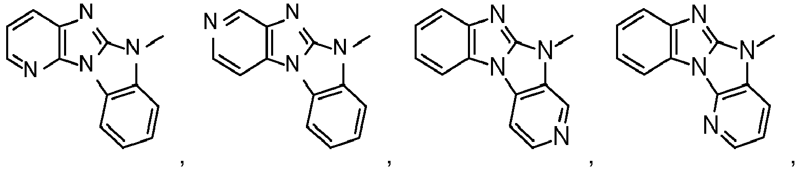


- If A1 is a group of formula (III), then A2 is a group of formula


- If A1 is a group of formula (II), then A2 is H, CN, -NR10R11, -Si(R12)(R13)(R14), a C6-C24aryl group, which can optionally be substituted by G; or a C2-C30heteroaryl group, which can optionally be substituted by G.
- The C6-C24aryl group A2, which optionally can be substituted by G, is typically phenyl, 4-methylphenyl, 4-methoxyphenyl, naphthyl, especially 1-naphthyl, or 2-naphthyl, biphenylyl, terphenylyl, pyrenyl, 2- or 9-fluorenyl, phenanthryl, or anthryl, or triphenylenyl (especially triphenylen-2-yl), which may be unsubstituted or substituted.
- The C2-C30heteroaryl group A2, which optionally can be substituted by G, represent a ring with five to seven ring atoms or a condensed ring system, wherein nitrogen, oxygen or sulfur are the possible hetero atoms, and is typically a heterocyclic group with five to 30 atoms having at least six conjugated π-electrons such as 9H-pyrido[2,3-b]indolyl, benzofuro[2,3-b]pyridyl, benzothiopheno[2,3-b]pyridyl, 9H-pyrido[2,3-c]indolyl, benzofuro[2,3-c]pyridyl, benzothiopheno[2,3-c]pyridyl, furo[3,2-b:4,5-b']dipyridyl, pyrrolo[3,2-b:4,5-b']dipyridyl, thieno[3,2-b:4,5-b']dipyridyl, thienyl, benzothiophenyl, dibenzothiophenyl, thianthrenyl, furyl, furfuryl, 2H-pyranyl, benzofuranyl, isobenzofuranyl, dibenzofuranyl, phenoxythienyl, pyrrolyl, imidazolyl, pyrazolyl, pyridyl, bipyridyl, triazinyl, pyrimidinyl, pyrazinyl, pyridazinyl, indolizinyl, isoindolyl, indolyl, indazolyl, purinyl, quinolizinyl, chinolyl, isochinolyl, phthalazinyl, naphthyridinyl, chinoxalinyl, chinazolinyl, cinnolinyl, pteridinyl, carbolinyl, benzotriazolyl, benzoxazolyl, phenanthridinyl, acridinyl, pyrimidinyl, phenanthrolinyl, phenazinyl, isothiazolyl, phenothiazinyl, isoxazolyl, furazanyl, benzimidazo[1,2-a]benzimidazo-5-yl, benzimidazo[1,2-a]benzimidazo-2-yl, benzimidazolo[2,1-b][1,3]benzothiazolyl, carbazolyl, 9-phenylcarbazolyl, azabenzimidazo[1,2-a]benzimidazolyl, or phenoxazinyl, which can be unsubstituted or substituted.
- The C6-C24aryl and C2-C30heteroaryl groups may be substituted by G.
- G is preferably C1-C18alkyl, such as methyl, ethyl, n-propyl, iso-propyl, n-butyl, isobutyl, sec-butyl, hexyl, octyl, or 2-ethyl-hexyl; -CF3, a C6-C14aryl group, a C6-C14aryl group, which is substituted by F, or C1-C18alkyl; a C2-C13heteroaryl group, or a C2-C13heteroaryl group, which is substituted by F, or C1-C18alkyl.
- Prefered C2-C30heteroaryl groups are pyridyl, triazinyl, pyrimidinyl, especially 9H-pyrido[2,3-b]indolyl, benzofuro[2,3-b]pyridyl, benzothiopheno[2,3-b]pyridyl, 9H-pyrido[2,3-c]indolyl, benzofuro[2,3-c]pyridyl, benzothiopheno[2,3-c]pyridyl, furo[3,2-b:4,5-b']dipyridyl, pyrrolo[3,2-b:4,5-b']dipyridyl, thieno[3,2-b:4,5-b']dipyridyl, benzimidazo[1,2-a]benzimidazo-5-yl


- Preferably, A2 is H, CN, a group of formula


X1, X2 and X3 are independently of each other N, or CH, with the proviso that at least one of
X1, X2 and X3 represent N;
R37 R38, R39, R40 and R41 are independently of each other H, -CN, or a phenyl group, and
R63 and R64 are independently of each other H, or a phenyl group. - Most preferred, A2 is a group of formula


- Specific examples of the compound represented by the formula (A) are given below. The compound represented by the formula (A) is not limited to the following specific examples.
- Examples of compounds of formula (I), wherein at least one of B1 to B16 is N are shown below:


- Compounds of formula (I), wherein at least one of R1, R2, R3, R4, R5, R6 and R7 is a C1-C25alkyl group; and/or at least a group Ar1, Ar2, A1 and/or A2 is substituted by a C1-C25alkyl group; are suitable materials for solution processable organic light emitting devices (OLEDs). Examples of such compounds are shown below:


- Examples of compounds of the formula

m is 1, n is 0, or 1, R1, R2, R3, R4, R5, R6 and R7 are H;


- Examples of compounds of the formula (I), wherein m is 1, n is 0, or 1, R1, R2, R3, R4, R5, R6 and R7 are H; Ar1 is


- Examples of compounds of the formula (I), wherein m is 1, n is 0, or 1, R1, R2, R3, R4, R5,
R6 and R7 are H; Ar1 and Ar2 are a group of formula


- Among the compounds of formula (I) compounds are preferred, wherein R1, R2, R3, R4, R5, R6, R7, Ar2, A1, A2, and n are defined above and below,
Ar1 is a group of formula
R8 is a C1-C25alkyl group, which can optionally be substituted by E and or interrupted by D; a C1-C25cycloalkyl group, which can optionally be substituted by E and or interrupted by D; a C6-C24aryl group, which can optionally be substituted by G; a C2-C30heteroaryl group, which can optionally be substituted by G. - Among the compounds of formula (I), compounds of formula

R2, R3, R4, R5, R6, R7, Ar2, A1, A2, and n are defined above and below,
X is O, S, or NR8 and
R8 is a C1-C25alkyl group, which can optionally be substituted by E and or interrupted by D; a C1-C25cycloalkyl group, which can optionally be substituted by E and or interrupted by D; a C6-C24aryl group, which can optionally be substituted by G; a C2-C30heteroaryl group, which can optionally be substituted by G. - Among the compounds of formula (Ia), compounds of formula

R2, R3, R4, R5, R6, R7, Ar2, A1, A2, X and n are defined above and below. - Among the compounds of formula (Ib) compounds of formula


R1, R2, R3, R4, R5, R6, R7, Ar2, A1, A2, X and n are defined above and below. Preferably, X is O, or S. - Examples of compounds of the formula

m is 1, n is 0, or 1, R1, R2, R3, R4, R5, R6 and R7 are H;
Ar1 is


- Compounds of formula (Ib-1) and (Ib-2) are even more preferred, wherein X is O, or S.
- In a particularly preferred embodiment the present invention is directed to compounds of formula


A1 is a group of formula


X1, X2 and X3 are independently of each other N, or CH, with the proviso that at least one of
X1, X2 and X3 represent N;
R37 R38, R39, R40 and R41 are independently of each other H, -CN, or a phenyl group, R63 and R64 are independently of each other H, or a phenyl group; or
A1 is a group of formula


X4, X5, X6, X7 and X8 are independently of each other N, or CH,
with the proviso that at least one of X4, X5 and X6 represents N;
with the proviso that at least one of X7 and X8 represents N;
R65 and R66 are independently of each other H, or a phenyl group, and
R8 is a phenyl group, or a group of formula
n is 0, or 1. - Examples of compounds of formula (Ib-1b) are shown below:


- Most preferred are compounds of formula


A1 is a group of formula


X1, X2 and X3 are independently of each other N, or CH, with the proviso that at least one of X1, X2 and X3 represent N;
R37 R38, R39, R40 and R41 are independently of each other H, -CN, or a phenyl group, R63 and R64 are independently of each other H, or a phenyl group; or
A1 is a group of formula


X4, X5, X6, X7 and X8 are independently of each other N, or CH,
with the proviso that at least one of X4, X5 and X6 represents N;
with the proviso that at least one of X7 and X8 represents N;
R65 and R66 are independently of each other H, or a phenyl group, and
R8 is a phenyl group, or a group of formula
n is 0, or 1. - Examples of compounds of formula (Ib-1a) are shown below:


- Examples of preferred compounds of formula I are compounds (C-8), (C-9), (C-12), (C-15), (C-16), (C-19), (C-21), (G-1), (G-2), (G-3), (G-4), (G-10), (H-1), (H-2), (H-3), and (H-10) shown above. Compounds (C-20), (C-22), (E-3), (E-4), (E-5), (E-6), (E-7), (E-8), (G-5), (G-6), (G-7), (G-8), (G-9), (G-12), (H-5), (H-6), (H-7), (H-8), (H-9), (H-11), and (H-12) are particularly preferred. Even more preferred are compounds, wherein A1 is a group of formula


- The synthesis of the compounds of formula (I) can be done in analogy to methods known in the literature.

- Heteroarylation can be affected, for example, by copper-catalyzed coupling of the compound of formula (XI) to the halogenated compound of the formula (XII) (X10 = Cl, Br, or I, especially Br, or I; Ullmann reaction).
- Reaction conditions for Ullmann reactions are, for example, described in Angew. Chem. Int. Ed. Engl., 48 (2009) 6954-71,
WO14009317 WO12130709 - Typically the Ullmann coupling of the compound of formula (XI) with a compound of formula (XII) is done in the presence of copper, or a copper salt, such as, for example, CuI, CuBr, Cu2O, or CuO, and a ligand, such as, for example, L-proline, trans-cyclohexane-1,2-diamine (DACH), 1,10-phenanthroline in a solvent, such as, for example, dimethylsulfoxide (DMSO), dimethylformamide (DMF), dimethylacetamide (DMA), N-methylpyrrolidone (NMP) and dioxane, or a solvent mixture. The reaction temperature is dependent on the reactivity of the starting materials, but is generally in the range of 25 to 200 °C.
- The synthesis of a compound of formula (XI),


- The introduction of the group


- Compounds of formula (I), wherein A1 is


- The synthesis of a compound of formula (XIV),

- The synthesis of

- Suitable base skeletons of the formula

WO2010079051 andEP1885818 . - The halogenation can be performed by methods known to those skilled in the art. Preference is given to brominating or iodinating in the 3 and 6 positions (dibromination) or in the 3 or 6 positions (monobromination) of the base skeleton of the formula 2,8 positions (dibenzofuran and dibenzothiophene) or 3,6 positions (carbazole).
- Optionally substituted dibenzofurans, dibenzothiophenes and carbazoles can be dibrominated in the 2,8 positions (dibenzofuran and dibenzothiophene) or 3,6 positions (carbazole) with bromine or NBS in glacial acetic acid or in chloroform. For example, the bromination with Br2 can be effected in glacial acetic acid or chloroform at low temperatures, e.g. 0°C. Suitable processes are described, for example, in M. Park, J.R. Buck, C.J. Rizzo, Tetrahedron, 54 (1998) 12707-12714 for X= NPh, and in W. Yang et al., J. Mater. Chem. 13 (2003) 1351 for X= S. In addition, 3,6-dibromocarbazole, 3,6-dibromo-9-phenylcarbazole, 2,8-dibromodibenzothiophene, 2,8-dibromodibenzofuran, 2-bromocarbazole, 3-bromodibenzothiophene, 3-bromodibenzofuran, 3-bromocarbazole, 2-bromodibenzothiophene and 2-bromodibenzofuran are commercially available.
- Monobromination in the 4 position of dibenzofuran (and analogously for dibenzothiophene) is described, for example, in J. Am. Chem. Soc. 1984, 106, 7150. Dibenzofuran (dibenzothiophene) can be monobrominated in the 3 position by a sequence known to those skilled in the art, comprising a nitration, reduction and subsequent Sandmeyer reaction.
- Monobromination in the 2 position of dibenzofuran or dibenzothiophene and monobromination in the 3 position of carbazole are effected analogously to the dibromination, with the exception that only one equivalent of bromine or NBS is added.
- Alternatively, it is also possible to utilize iodinated dibenzofurans, dibenzothiophenes and carbazoles. The preparation is described, inter alia, in Tetrahedron. Lett. 47 (2006) 6957-6960, Eur. J. Inorg. Chem. 24 (2005) 4976-4984, J. Heterocyclic Chem. 39 (2002) 933-941, J. Am. Chem. Soc. 124 (2002) 11900-11907, J. Heterocyclic Chem, 38 (2001) 77-87.
- For the nucleophilic substitution, CI- or F-substituted dibenzofurans, dibenzothiophenes and carbazoles are required. The chlorination is described, inter alia, in J. Heterocyclic Chemistry, 34 (1997) 891-900, Org. Lett., 6 (2004) 3501-3504; J. Chem. Soc. [Section] C: Organic, 16 (1971) 2775-7, Tetrahedron Lett. 25 (1984) 5363-6, J. Org. Chem. 69 (2004) 8177-8182. The fluorination is described in J. Org. Chem. 63 (1998) 878-880 and J. Chem. Soc., Perkin Trans. 2, 5 (2002) 953-957.
- Compounds of formula


- Compounds of formula

Ar1 is a group of formula


A2 is a group of formula
- Examples of compounds of formula (XIII) are shown below:


- Compounds (Z-1), (Z-2), (Z-5) and (Z-6) are preferred. Compounds (Z-1) and (Z-2) are most preferred.
- Halogen is fluorine, chlorine, bromine and iodine.
- C1-C25alkyl (C1-C18alkyl) is typically linear or branched, where possible. Examples are methyl, ethyl, n-propyl, isopropyl, n-butyl, sec.-butyl, isobutyl, tert.-butyl, n-pentyl, 2-pentyl, 3-pentyl, 2,2-dimethylpropyl, 1,1,3,3-tetramethylpentyl, n-hexyl, 1-methylhexyl, 1,1,3,3,5,5-hexamethylhexyl, n-heptyl, isoheptyl, 1,1,3,3-tetramethylbutyl, 1-methylheptyl, 3-methylheptyl, n-octyl, 1,1,3,3-tetramethylbutyl and 2-ethylhexyl, n-nonyl, decyl, undecyl, dodecyl, tridecyl, tetradecyl, pentadecyl, hexadecyl, heptadecyl, or octadecyl. C1-C8alkyl is typically methyl, ethyl, n-propyl, isopropyl, n-butyl, sec.-butyl, isobutyl, tert.-butyl, n-pentyl, 2-pentyl, 3-pentyl, 2,2-dimethyl-propyl, n-hexyl, n-heptyl, n-octyl, 1,1,3,3-tetramethylbutyl and 2-ethylhexyl. C1-C4alkyl is typically methyl, ethyl, n-propyl, isopropyl, n-butyl, sec.-butyl, isobutyl, tert.-butyl.
- C1-C25alkoxy groups (C1-C18alkoxy groups) are straight-chain or branched alkoxy groups, e.g. methoxy, ethoxy, n-propoxy, isopropoxy, n-butoxy, sec-butoxy, tert-butoxy, amyloxy, isoamyloxy or tert-amyloxy, heptyloxy, octyloxy, isooctyloxy, nonyloxy, decyloxy, undecyloxy, dodecyloxy, tetradecyloxy, pentadecyloxy, hexadecyloxy, heptadecyloxy and octadecyloxy. Examples of C1-C8alkoxy are methoxy, ethoxy, n-propoxy, isopropoxy, n-butoxy, sec.-butoxy, isobutoxy, tert.-butoxy, n-pentyloxy, 2-pentyloxy, 3-pentyloxy, 2,2-dimethylpropoxy, n-hexyloxy, n-heptyloxy, n-octyloxy, 1,1,3,3-tetramethylbutoxy and 2-ethylhexyloxy, preferably C1-C4alkoxy such as typically methoxy, ethoxy, n-propoxy, isopropoxy, n-butoxy, sec.-butoxy, isobutoxy, tert.-butoxy.
- The term "cycloalkyl group" is typically C5-C12cycloalkyl, such as cyclopentyl, cyclohexyl, cycloheptyl, cyclooctyl, cyclononyl, cyclodecyl, cycloundecyl, cyclododecyl, preferably cyclopentyl, cyclohexyl, cycloheptyl, or cyclooctyl, which may be unsubstituted or substituted.
- C6-C24aryl (C6-C18aryl), which optionally can be substituted, is typically phenyl, 4-methylphenyl, 4-methoxyphenyl, naphthyl, especially 1-naphthyl, or 2-naphthyl, biphenylyl, terphenylyl, pyrenyl, 2- or 9-fluorenyl, phenanthryl, or anthryl, which may be unsubstituted or substituted. Phenyl, 1-naphthyl and 2-naphthyl are examples of a C6-C10aryl group.
- C6-C24aryloxy, which optionally can be substituted, is typically C6-C10aryloxy, which optionally can be substituted by one, or more C1-C8alkyl and/or C1-C8alkoxy groups, such as, for example, phenoxy, 1-naphthoxy, or 2-naphthoxy.
- C7-C25aralkyl is typically benzyl, 2-benzyl-2-propyl, β-phenyl-ethyl, α,α-dimethylbenzyl, ω-phenyl-butyl, ω,ω-dimethyl-ω-phenyl-butyl, ω-phenyl-dodecyl, ω-phenyl-octadecyl, ω-phenyl-eicosyl or ω-phenyl-docosyl, preferably C7-C18aralkyl such as benzyl, 2-benzyl-2-propyl, β-phenyl-ethyl, α,α-dimethylbenzyl, ω-phenyl-butyl, ω,ω-dimethyl-ω-phenyl-butyl, ω-phenyl-dodecyl or ω-phenyl-octadecyl, and particularly preferred C7-C12aralkyl such as benzyl, 2-benzyl-2-propyl, β-phenyl-ethyl, α,α-dimethylbenzyl, ω-phenyl-butyl, or ω,ω-dimethyl-ω-phenyl-butyl, in which both the aliphatic hydrocarbon group and aromatic hydrocarbon group may be unsubstituted or substituted. Preferred examples are benzyl, 2-phenylethyl, 3-phenylpropyl, naphthylethyl, naphthylmethyl, and cumyl.
- C2-C30heteroaryl represents a ring with five to seven ring atoms or a condensed ring system, wherein nitrogen, oxygen or sulfur are the possible hetero atoms, and is typically a heterocyclic group with five to 30 atoms having at least six conjugated π-electrons such as thienyl, benzothiophenyl, dibenzothiophenyl, thianthrenyl, furyl, furfuryl, 2H-pyranyl, benzofuranyl, isobenzofuranyl, dibenzofuranyl, phenoxythienyl, pyrrolyl, imidazolyl, pyrazolyl, pyridyl, bipyridyl, triazinyl, pyrimidinyl, pyrazinyl, pyridazinyl, indolizinyl, isoindolyl, indolyl, indazolyl, purinyl, quinolizinyl, chinolyl, isochinolyl, phthalazinyl, naphthyridinyl, chinoxalinyl, chinazolinyl, cinnolinyl, pteridinyl, carbazolyl, carbolinyl, benzotriazolyl, benzoxazolyl, phenanthridinyl, acridinyl, pyrimidinyl, phenanthrolinyl, phenazinyl, isothiazolyl, phenothiazinyl, isoxazolyl, furazanyl, 4-imidazo[1,2-a]benzimidazoyl, 5-benzimidazo[1,2-a]benzimidazoyl, benzimidazolo[2,1-b][1,3]benzothiazolyl, carbazolyl, or phenoxazinyl, which can be unsubstituted or substituted. Benzimidazo[1,2-a]benzimidazo-5-yl, benzimidazo[1,2-a]benzimidazo-2-yl, carbazolyl and dibenzofuranyl are examples of a C2-C14heteroaryl group.
- C6-C24arylene groups, which optionally can be substituted by G, are typically phenylene, 4-methylphenylene, 4-methoxyphenylene, naphthylene, especially 1-naphthylene, or 2-naphthylene, biphenylylene, terphenylylene, pyrenylene, 2- or 9-fluorenylene, phenanthrylene, or anthrylene, which may be unsubstituted or substituted. Preferred C6-C24arylene groups are 1,3-phenylene, 3,3'-biphenylylene, 3,3'-m-terphenylene, 2- or 9-fluorenylene, phenanthrylene, which may be unsubstituted or substituted.
- C2-C30heteroarylene groups, which optionally can be substituted by G, represent a ring with five to seven ring atoms or a condensed ring system, wherein nitrogen, oxygen or sulfur are the possible hetero atoms, and is typically a heterocyclic group with five to 30 atoms having at least six conjugated -electrons such as thienylene, benzothiophenylene, dibenzothiophenylene, thianthrenylene, furylene, furfurylene, 2H-pyranylene, benzofuranylene, isobenzofuranylene, dibenzofuranylene, phenoxythienylene, pyrrolylene, imidazolylene, pyrazolylene, pyridylene, bipyridylene, triazinylene, pyrimidinylene, pyrazinylene, pyridazinylene, indolizinylene, isoindolylene, indolylene, indazolylene, purinylene, quinolizinylene, chinolylene, isochinolylene, phthalazinylene, naphthyridinylene, chinoxalinylene, chinazolinylene, cinnolinylene, pteridinylene, carbolinylene, benzotriazolylene, benzoxazolylene, phenanthridinylene, acridinylene, pyrimidinylene, phenanthrolinylene, phenazinylene, isothiazolylene, phenothiazinylene, isoxazolylene, furazanylene, carbazolylene, benzimidazo[1,2-a]benzimidazo-2,5-ylene, or phenoxazinylene, which can be unsubstituted or substituted. Preferred C2-C30heteroarylene groups are pyridylene, triazinylene, pyrimidinylene, carbazolylene, dibenzofuranylene and benzimidazo[1,2-a]benzimidazo-2,5-ylene

- Possible substituents of the above-mentioned groups are C1-C8alkyl, a hydroxyl group, a mercapto group, C1-C8alkoxy, C1-C8alkylthio, halogen, halo-C1-C8alkyl, or a cyano group. The C6-C24aryl (C6-C18aryl) and C2-C30heteroaryl groups are preferably substituted by one, or more C1-C8alkyl groups.
- If a substituent occurs more than one time in a group, it can be different in each occurrence.
- Halo-C1-C8alkyl is an alkyl group where at least one of the hydrogen atoms is replaced by a halogen atom. Examples are -CF3, -CF2CF3, -CF2CF2CF3, -CF(CF3)2, -(CF2)3CF3, and -C(CF3)3.
- The wording "substituted by G" means that one, or more, especially one to three substituents G might be present.
- As described above, the aforementioned groups may be substituted by E and/or, if desired, interrupted by D. Interruptions are of course possible only in the case of groups containing at least 2 carbon atoms connected to one another by single bonds; C6-C18aryl is not interrupted; interrupted arylalkyl contains the unit D in the alkyl moiety. C1-C18alkyl substituted by one or more E and/or interrupted by one or more units D is, for example, (CH2CH2O)1-9-Rx, where Rx is H or C1-C10alkyl or C2-C10alkanoyl (e.g. CO-CH(C2H5)C4H9), CH2-CH(ORy')-CH2-O-Ry, where Ry is C1-C18alkyl, C5-C12cycloalkyl, phenyl, C7-C15phenylalkyl, and Ry' embraces the same definitions as Ry or is H;
- C1-C8alkylene-COO-Rz, e.g. CH2COORz, CH(CH3)COORz, C(CH3)2COORz, where Rz is H, C1-C18alkyl, (CH2CH2O)1-9-Rx, and Rx embraces the definitions indicated above; CH2CH2-O-CO-CH=CH2; CH2CH(OH)CH2-O-CO-C(CH3)=CH2.
- An alkyl group substituted by E is, for example, an alkyl group where at least one of the hydrogen atoms is replaced by F. Examples are -CF3, -CF2CF3, -CF2CF2CF3, -CF(CF3)2, -(CF2)3CF3, and -C(CF3)3.
- It has been found that the compounds of the formula I are particularly suitable for use in applications in which charge carrier conductivity is required, especially for use in organic electronics applications, for example selected from switching elements such as organic transistors, e.g. organic FETs and organic TFTs, organic solar cells and organic light-emitting diodes (OLEDs), the compounds of the formula I being particularly suitable in OLEDs for use as matrix material in a light-emitting layer and/or as electron and/or exciton blocker material and/or as hole and/or exciton blocker material, especially in combination with a phosphorescence emitter. In the case of use of the inventive compounds of the formula I in OLEDs, OLEDs which have good efficiencies and a long lifetime and which can be operated especially at a low use and operating voltage are obtained. The inventive compounds of the formula I are suitable especially for use as matrix and/or charge/exciton blocker materials for blue and green emitters, for example light blue or deep blue emitters, these being especially phosphorescence emitters. Furthermore, the compounds of the formula I can be used as conductor/complementary materials in organic electronics applications selected from switching elements and organic solar cells.
- The compounds of the formula I can be used as matrix material and/or charge/exciton blocker material and/or charge transport material (charge conductor material). The inventive compounds of the formula I are preferably used as matrix materials in organic electronics applications, especially in OLEDs.
- In the emission layer or one of the emission layers of an OLED, it is also possible to combine an emitter material with a matrix material of the compound of the formula I and a further matrix material. This may achieve a high quantum efficiency of this emission layer. When a compound of the formula I is used as matrix (host) material in an emission layer and additionally as charge/exciton blocker material, owing to the chemical identity or similarity of the materials, an improved interface between the emission layer and the adjacent charge/exciton blocker material, which can lead to a decrease in the voltage with equal luminance and to an extension of the lifetime of the OLED. Moreover, the use of the same material for charge/exciton blocker material and for the matrix of an emission layer allows the production process of an OLED to be simplified, since the same source can be used for the vapor deposition process of the material of one of the compounds of the formula I.
- Suitable structures of organic electronic devices are known to those skilled in the art and are specified below.
- The organic transistor generally includes a semiconductor layer formed from an organic layer with charge transport capacity; a gate electrode formed from a conductive layer; and an insulating layer introduced between the semiconductor layer and the conductive layer. A source electrode and a drain electrode are mounted on this arrangement in order thus to produce the transistor element. In addition, further layers known to those skilled in the art may be present in the organic transistor.
- The organic solar cell (photoelectric conversion element) generally comprises an organic layer present between two plate-type electrodes arranged in parallel. The organic layer may be configured on a comb-type electrode. There is no particular restriction regarding the site of the organic layer and there is no particular restriction regarding the material of the electrodes. When, however, plate-type electrodes arranged in parallel are used, at least one electrode is preferably formed from a transparent electrode, for example an ITO electrode or a fluorine-doped tin oxide electrode. The organic layer is formed from two sublayers, i.e. a layer with p-type semiconductor properties or hole transport capacity, and a layer formed with n-type semiconductor properties or charge transport capacity. In addition, it is possible for further layers known to those skilled in the art to be present in the organic solar cell. The layers with charge transport capacity may comprise the compounds of formula I.
- It is likewise possible that the compounds of the formula I are present both in the light-emitting layer (preferably as matrix material) and in the blocking layers (as charge/exciton blockers).
- The present invention further provides an organic light-emitting diode comprising an anode (a) and a cathode (i) and a light-emitting layer (e) arranged between the anode (a) and the cathode (i), and if appropriate at least one further layer selected from the group consisting of at least one blocking layer for holes/excitons, at least one blocking layer for electrons/excitons, at least one hole injection layer, at least one hole transport layer, at least one electron injection layer and at least one electron transport layer, wherein the at least one compound of the formula I is present in the light-emitting layer (e) and/or in at least one of the further layers. The at least one compound of the formula I is preferably present in the light-emitting layer and/or the charge/exciton blocking layers.
- In a preferred embodiment of the present invention, at least one compound of the formula I, especially a compound of formula (Ib-1), or (Ib-2), very especially a compound of the formula (Ib-1a), or (Ib-2a), is used as charge transport material. Examples of preferred compounds of formula I are (C-8), (C-9), (C-12), (C-15), (C-16), (C-19), (C-21), (G-1), (G-2), (G-3), (G-4), (G-10), (H-1), (H-2), (H-3), and (H-10) shown above. Compounds (C-20), (C-22), (E-3), (E-4), (E-5), (E-6), (E-7), (E-8), (G-5), (G-6), (G-7), (G-8), (G-9), (G-12), (H-5), (H-6), (H-7), (H-8), (H-9), (H-11), and (H-12) are particularly preferred.
- In another preferred embodiment of the present invention, at least one compound of the formula I, especially a compound of formula (Ib-1), or (Ib-2), very especially a compound of the formula (Ib-1a), or (Ib-2a), is used as charge/exciton blocker material. Examples of preferred compounds of formula I are (C-8), (C-9), (C-12), (C-15), (C-16), (C-19), (C-21), (G-1), (G-2), (G-3), (G-4), (G-10), (H-1), (H-2), (H-3), and (H-10) shown above. Compounds Compounds (C-20), (C-22), (E-3), (E-4), (E-5), (E-6), (E-7), (E-8), (G-5), (G-6), (G-7), (G-8), (G-9), (G-12), (H-5), (H-6), (H-7), (H-8), (H-9), (H-11), and (H-12) are particularly preferred.
- The present application further relates to a light-emitting layer comprising at least one compound of the formula I.
- The inventive organic light-emitting diode (OLED) thus generally has the following structure: an anode (a) and a cathode (i) and a light-emitting layer (e) arranged between the anode (a) and the cathode (i).
- The inventive OLED may, for example - in a preferred embodiment - be formed from the following layers:
- 1. Anode (a)
- 2. Hole transport layer (c)
- 3. Light-emitting layer (e)
- 4. Blocking layer for holes/excitons (f)
- 5. Electron transport layer (g)
- 6. Cathode (i)
- Layer sequences different than the aforementioned structure are also possible, and are known to those skilled in the art. For example, it is possible that the OLED does not have all of the layers mentioned; for example, an OLED with layers (a) (anode), (e) (light-emitting layer) and (i) (cathode) is likewise suitable, in which case the functions of the layers (c) (hole transport layer) and (f) (blocking layer for holes/excitons) and (g) (electron transport layer) are assumed by the adjacent layers. OLEDs which have layers (a), (c), (e) and (i), or layers (a), (e), (f), (g) and (i), are likewise suitable. In addition, the OLEDs may have a blocking layer for electrons/excitons (d) between the hole transport layer (c) and the Light-emitting layer (e).
- It is additionally possible that a plurality of the aforementioned functions (electron/exciton blocker, hole/exciton blocker, hole injection, hole conduction, electron injection, electron conduction) are combined in one layer and are assumed, for example, by a single material present in this layer. For example, a material used in the hole transport layer, in one embodiment, may simultaneously block excitons and/or electrons.
- Furthermore, the individual layers of the OLED among those specified above may in turn be formed from two or more layers. For example, the hole transport layer may be formed from a layer into which holes are injected from the electrode, and a layer which transports the holes away from the hole-injecting layer into the light-emitting layer. The electron conduction layer may likewise consist of a plurality of layers, for example a layer in which electrons are injected by the electrode, and a layer which receives electrons from the electron injection layer and transports them into the light-emitting layer. These layers mentioned are each selected according to factors such as energy level, thermal resistance and charge carrier mobility, and also energy difference of the layers specified with the organic layers or the metal electrodes. The person skilled in the art is capable of selecting the structure of the OLEDs such that it is matched optimally to the organic compounds used in accordance with the invention.
- In a preferred embodiment the OLED according to the present invention comprises in this order:
- (a) an anode,
- (b) optionally a hole injection layer,
- (c) optionally a hole transport layer,
- (d) optionally an exciton blocking layer
- (e) an emitting layer,
- (f) optionally a hole/ exciton blocking layer
- (g) optionally an electron transport layer,
- (h) optionally an electron injection layer, and
- (i) a cathode.
- In a particularly preferred embodiment the OLED according to the present invention comprises in this order:
- (a) an anode,
- (b) optionally a hole injection layer,
- (c) a hole transport layer,
- (d) an exciton blocking layer
- (e) an emitting layer,
- (f) a hole/ exciton blocking layer
- (g) an electron transport layer, and
- (h) optionally an electron injection layer, and
- (i) a cathode.
- The properties and functions of these various layers, as well as example materials are known from the prior art and are described in more detail below on basis of preferred embodiments.
- The anode is an electrode which provides positive charge carriers. It may be composed, for example, of materials which comprise a metal, a mixture of different metals, a metal alloy, a metal oxide or a mixture of different metal oxides. Alternatively, the anode may be a conductive polymer. Suitable metals comprise the metals of groups 11, 4, 5 and 6 of the Periodic Table of the Elements, and also the transition metals of groups 8 to 10. When the anode is to be transparent, mixed metal oxides of groups 12, 13 and 14 of the Periodic Table of the Elements are generally used, for example indium tin oxide (ITO). It is likewise possible that the anode (a) comprises an organic material, for example polyaniline, as described, for example, in Nature, Vol. 357, pages 477 to 479 (June 11, 1992). Preferred anode materials include conductive metal oxides, such as indium tin oxide (ITO) and indium zinc oxide (IZO), aluminum zinc oxide (AlZnO), and metals. Anode (and substrate) may be sufficiently transparent to create a bottom-emitting device. A preferred transparent substrate and anode combination is commercially available ITO (anode) deposited on glass or plastic (substrate). A reflective anode may be preferred for some top-emitting devices, to increase the amount of light emitted from the top of the device. At least either the anode or the cathode should be at least partly transparent in order to be able to emit the light formed. Other anode materials and structures may be used.
- Generally, injection layers are comprised of a material that may improve the injection of charge carriers from one layer, such as an electrode or a charge generating layer, into an adjacent organic layer. Injection layers may also perform a charge transport function. The hole injection layer may be any layer that improves the injection of holes from anode into an adjacent organic layer. A hole injection layer may comprise a solution deposited material, such as a spin-coated polymer, or it may be a vapor deposited small molecule material, such as, for example, CuPc or MTDATA. Polymeric hole-injection materials can be used such as poly(N-vinylcarbazole) (PVK), polythiophenes, polypyrrole, polyaniline, self-doping polymers, such as, for example, sulfonated poly(thiophene-3-[2[(2-methoxyethoxy)ethoxy]-2,5-diyl) (Plexcore® OC Conducting Inks commercially available from Plextronics), and copolymers such as poly(3,4-ethylenedioxythiophene)/poly(4-styrenesulfonate) also called PEDOT/PSS.
- Either hole-transporting molecules or polymers may be used as the hole transport material. Suitable hole transport materials for layer (c) of the inventive OLED are disclosed, for example, in Kirk-Othmer Encyclopedia of Chemical Technology, 4th Edition, Vol. 18, pages 837 to 860, 1996,
US20070278938 ,US2008/0106190 ,US2011/0163302 (triarylamines with (di)benzothiophen/(di)benzofuran; Nan-Xing Hu et al. Synth. Met. 111 (2000) 421 (indolocarbazoles),WO2010002850 (substituted phenylamine compounds) and -
WO2012/16601 WO2012/16601 WO2013/022419 , wherein


- In a preferred embodiment it is possible to use metal carbene complexes as hole transport materials. Suitable carbene complexes are, for example, carbene complexes as described in
WO2005/019373A2 ,WO2006/056418 A2 ,WO2005/113704 ,WO2007/115970 ,WO2007/115981 ,WO2008/000727 andPCT/EP2014/055520 
- Another example of a suitable carbene complex is Ir(ABIC)3 with the Ia:

- The hole-transporting layer may also be electronically doped in order to improve the transport properties of the materials used, in order firstly to make the layer thicknesses more generous (avoidance of pinholes/short circuits) and in order secondly to minimize the operating voltage of the device. Electronic doping is known to those skilled in the art and is disclosed, for example, in W. Gao, A. Kahn, J. Appl. Phys., Vol. 94, 2003, 359 (p-doped organic layers); A. G. Werner, F. Li, K. Harada, M. Pfeiffer, T. Fritz, K. Leo, Appl. Phys. Lett., Vol. 82, No. 25, 2003, 4495 and Pfeiffer et al., Organic Electronics 2003, 4, 89 - 103 and K. Walzer, B. Maennig, M. Pfeiffer, K. Leo, Chem. Soc. Rev. 2007, 107, 1233. For example it is possible to use mixtures in the hole-transporting layer, in particular mixtures which lead to electrical p-doping of the hole-transporting layer. p-Doping is achieved by the addition of oxidizing materials. These mixtures may, for example, be the following mixtures: mixtures of the abovementioned hole transport materials with at least one metal oxide, for example MoO2, MoO3, WOx, ReO3 and/or V2O5, preferably MoO3 and/or ReO3, more preferably MoO3, or mixtures comprising the aforementioned hole transport materials and one or more compounds selected from 7,7,8,8-tetracyanoquinodimethane (TCNQ), 2,3,5,6-tetrafluoro-7,7,8,8-tetracyanoquinodimethane (F4-TCNQ), 2,5-bis(2-hydroxyethoxy)-7,7,8,8-tetracyanoquinodimethane, bis(tetra-n-butylammonium)tetracyanodiphenoquinodimethane, 2,5-dimethyl-7,7,8,8-tetracyanoquinodimethane, tetracyanoethylene, 11,11,12,12-tetracyanonaphtho2,6-quinodimethane, 2-fluoro-7,7,8,8-tetracyanoquino-dimethane, 2,5-difluoro-7,7,8,8etracyanoquinodimethane, dicyanomethylene-1,3,4,5,7,8-hexafluoro-6H-naphthalen-2-ylidene)malononitrile (F6-TNAP), Mo(tfd)3 (from Kahn et al., J. Am. Chem. Soc. 2009, 131 (35), 12530-12531), compounds as described in
EP1988587 ,US2008265216 ,EP2180029 ,US20100102709 ,WO2010132236 ,EP2180029 and quinone compounds as mentioned inEP2401254 . Preferred mixtures comprise the aforementioned carbene complexes, such as, for example, the carbene complexes HTM-1 and HTM-2, and MoO3 and/or ReO3, especially MoO3. In a particularly preferred embodiment the hole transport layer comprises from 0.1 to 10 wt % of MoO3 and 90 to 99.9 wt % carbene complex, especially of the carbene complex HTM-1 and HTM-2, wherein the total amount of the MoO3 and the carbene complex is 100 wt %. - Blocking layers may be used to reduce the number of charge carriers (electrons or holes) and/or excitons that leave the emissive layer. An electron/exciton blocking layer (d) may be disposed between the first emitting layer (e) and the hole transport layer (c), to block electrons from emitting layer (e) in the direction of hole transport layer (c). Blocking layers may also be used to block excitons from diffusing out of the emissive layer. Suitable metal complexes for use as electron/exciton blocker material are, for example, carbene complexes as described in
WO2005/019373A2 ,WO2006/056418A2 ,WO2005/113704 ,WO2007/115970 ,WO2007/115981 ,WO2008/000727 andPCT/EP2014/055520 - The light-emitting layer (e) comprises at least one emitter material. In principle, it may be a fluorescence or phosphorescence emitter, suitable emitter materials being known to those skilled in the art. The at least one emitter material is preferably a phosphorescence emitter. The phosphorescence emitter compounds used with preference are based on metal complexes, and especially the complexes of the metals Ru, Rh, Ir, Pd and Pt, in particular the complexes of Ir, have gained significance. The compounds of the formula I can be used as the matrix in the light-emitting layer.
- Suitable metal complexes for use in the inventive OLEDs are described, for example, in documents
WO 02/60910 A1 US 2001/0015432 A1 ,US 2001/0019782 A1 ,US 2002/0055014 A1 ,US 2002/0024293 A1 ,US 2002/0048689 A1 ,EP 1 191 612 A2 ,EP 1 191 613 A2 ,EP 1 211 257 A2 ,US 2002/0094453 A1 ,WO 02/02714 A2 WO 00/70655 A2 WO 01/41512 A1 WO 02/15645 A1 WO 2005/019373 A2 ,WO 2005/113704 A2 ,WO 2006/115301 A1 ,WO 2006/067074 A1 ,WO 2006/056418 ,WO 2006121811 A1 ,WO 2007095118 A2 ,WO 2007/115970 ,WO 2007/115981 ,WO 2008/000727 ,WO2010129323 ,WO2010056669 ,WO10086089 US2011/0057559 ,WO2011/106344 ,US2011/0233528 ,WO2012/048266 andWO2012/172482 . - Further suitable metal complexes are the commercially available metal complexes tris(2-phenylpyridine)iridium(III), iridium(III) tris(2-(4-tolyl)pyridinato-N,C2'), bis(2-phenylpyridine)(acetylacetonato)iridium(III), iridium(III) tris(1-phenylisoquinoline), iridium(III) bis(2,2'-benzothienyl)pyridinato-N,C3')(acetylacetonate), tris(2-phenylquinoline)iridium(III), iridium(III) bis(2-(4,6-difluorophenyl)pyridinato-N,C2)picolinate, iridium(III) bis(1-phenylisoquinoline)(acetylacetonate), bis(2-phenylquinoline)(acetylacetonato)iridium(III), iridium(III) bis(di-benzo[f,h]quinoxaline)(acetylacetonate), iridium(III) bis(2-methyldi-benzo[f,h]quinoxaline)(acetylacetonate) and tris(3-methyl-1-phenyl-4-trimethylacetyl-5-pyrazolino)terbium(III), bis[1-(9,9-dimethyl-9H-fluoren-2-yl)isoquinoline](acetyl-acetonato)iridium(III), bis(2-phenylbenzothiazolato)(acetylacetonato)iridium(III), bis(2-(9,9-dihexylfluorenyl)-1-pyridine)(acetylacetonato)iridium(III), bis(2-benzo[b]thiophen-2-yl-pyridine)(acetylacetonato)iridium(III).
- In addition, the following commercially available materials are suitable: tris(dibenzoylacetonato)mono(phenanthroline)europium(III), tris(dibenzoylmethane)-mono(phenanthroline)europium(III), tris(dibenzoylmethane)mono(5-aminophenanthroline)-europium(III), tris(di-2-naphthoylmethane)mono(phenanthroline)europium(III), tris(4-bromobenzoylmethane)mono(phenanthroline)europium(III), tris(di(biphenyl)methane)-mono(phenanthroline)europium(III), tris(dibenzoylmethane)mono(4,7-diphenyl-phenanthroline)europium(III), tris(dibenzoylmethane)mono(4,7-di-methyl-phenanthroline)europium(III), tris(dibenzoylmethane)mono(4,7-dimethylphenan-throlinedisulfonic acid)europium(III) disodium salt, tris[di(4-(2-(2-ethoxyethoxy)ethoxy)-benzoylmethane)]mono(phenanthroline)europium(III) and tris[di[4-(2-(2-ethoxy-ethoxy)ethoxy)benzoylmethane)]mono(5-aminophenanthroline)europium(III), osmium(II) bis(3-(trifluoromethyl)-5-(4-tert-butylpyridyl)-1,2,4-triazolato)diphenylmethylphosphine, osmium(II) bis(3-(trifluoromethyl)-5-(2-pyridyl)-1,2,4-triazole)dimethylphenylphosphine, osmium(II) bis(3-(trifluoromethyl)-5-(4-tert-butylpyridyl)-1,2,4-triazolato)dimethylphenylphosphine, osmium(II) bis(3-(trifluoromethyl)-5-(2-pyridyl)-pyrazolato)dimethylphenylphosphine, tris[4,4'-di-tert-butyl(2,2')-bipyridine]ruthenium(III), osmium(II) bis(2-(9,9-dibutylfluorenyl)-1-isoquinoline(acetylacetonate).
- Preferred phosphorescence emitters are carbene complexes. Suitable phosphorescent blue emitters are specified in the following publications:
WO2006/056418A2 ,WO2005/113704 ,WO2007/115970 ,WO2007/115981 ,WO2008/000727 ,WO2009050281 ,WO2009050290 ,WO2011051404 ,US2011/057559 WO2011/073149 ,WO2012/121936A2 ,US2012/0305894A1 ,WO2012/170571 ,WO2012/170461 ,WO2012/170463 ,WO2006/121811 ,WO2007/095118 ,WO2008/156879 ,WO2008/156879 ,WO2010/068876 ,US2011/0057559 ,WO2011/106344 ,US2011/0233528 ,WO2012/048266 ,WO2012/172482 ,PCT/EP2014/064054 PCT/EP2014/066272 - Preferably, the light emitting layer (e) comprises at least one carbine complex as phosphorescence emitter. Suitable carbine complexes are, for example, compounds of the formula

WO 2005/019373 A2 , wherein the symbols have the following meanings: - M is a metal atom selected from the group consisting of Co, Rh, Ir, Nb, Pd, Pt, Fe, Ru, Os, Cr, Mo, W, Mn, Tc, Re, Cu, Ag and Au in any oxidation state possible for the respective metal atom;
- Carbene is a carbene ligand which may be uncharged or monoanionic and monodentate, bidentate or tridentate, with the carbene ligand also being able to be a biscarbene or triscarbene ligand;
- L is a monoanionic or dianionic ligand, which may be monodentate or bidentate;
- K is an uncharged monodentate or bidentate ligand selected from the group consisting of phosphines; phosphonates and derivatives thereof, arsenates and derivatives thereof;
- phosphites; CO; pyridines; nitriles and conjugated dienes which form a π complex with M1; n1 is the number of carbene ligands, where n1 is at least 1 and when n1 > 1 the carbene ligands in the complex of the formula I can be identical or different;
- m1 is the number of ligands L, where m1 can be 0 or ≥ 1 and when m1 > 1 the ligands L can be identical or different;
- o is the number of ligands K, where o can be 0 or ≥ 1 and when o > 1 the ligands K can be identical or different;
- where the sum n1 + m1 + o is dependent on the oxidation state and coordination number of the metal atom and on the denticity of the ligands carbene, L and K and also on the charge on the ligands, carbene and L, with the proviso that n1 is at least 1.
- More preferred are metal-carbene complexes of the general formula

WO2011/073149 ,
where M is Ir, or Pt,
n1 is an integer selected from 1, 2 and 3,
Y is NR51', O, S or C(R25')2,
A2', A3', A4', and A5' are each independently N or C, where 2 A' = nitrogen atoms and at least one carbon atom is present between two nitrogen atoms in the ring,
R51' is a linear or branched alkyl radical optionally interrupted by at least one heteroatom, optionally bearing at least one functional group and having 1 to 20 carbon atoms, cycloalkyl radical optionally interrupted by at least one heteroatom, optionally bearing at least one functional group and having 3 to 20 carbon atoms, substituted or unsubstituted aryl radical optionally interrupted by at least one heteroatom, optionally bearing at least one functional group and having 6 to 30 carbon atoms, substituted or unsubstituted heteroaryl radical optionally interrupted by at least one heteroatom, optionally bearing at least one functional group and having a total of 5 to 18 carbon atoms and/or heteroatoms,
R52', R53', R54' and R55' are each, if A2', A3', A4' and/or A5' is N, a free electron pair, or, if A2', A3', A4' and/or A5' is C, each independently hydrogen, linear or branched alkyl radical optionally interrupted by at least one heteroatom, optionally bearing at least one functional group and having 1 to 20 carbon atoms, cycloalkyl radical optionally interrupted by at least one heteroatom, optionally bearing at least one functional group and having 3 to 20 carbon atoms, substituted or unsubstituted aryl radical optionally interrupted by at least one heteroatom, optionally bearing at least one functional group and having 6 to 30 carbon atoms, substituted or unsubstituted heteroaryl radical optionally interrupted by at least one heteroatom, optionally bearing at least one functional group and having a total of 5 to 18 carbon atoms and/or heteroatoms, group with donor or acceptor action, or R53' and R54' together with A3' and A4' form an optionally substituted, unsaturated ring optionally interrupted by at least one further heteroatom and having a total of 5 to 18 carbon atoms and/or heteroatoms,
R56', R57', R58' and R59' are each independently hydrogen, linear or branched alkyl radical optionally interrupted by at least one heteroatom, optionally bearing at least one functional group and having 1 to 20 carbon atoms, cycloalkyl radical optionally interrupted by at least one heteroatom, optionally bearing at least one functional group and having 3 to 20 carbon atoms, cycloheteroalkyl radical optionally interrupted by at least one heteroatom, optionally bearing at least one functional group and having 3 to 20 carbon atoms, substituted or unsubstituted aryl radical optionally interrupted by at least one heteroatom, optionally bearing at least one functional group and having 6 to 30 carbon atoms, substituted or unsubstituted heteroaryl radical optionally interrupted by at least one heteroatom, optionally bearing at least one functional group and having a total of 5 to 18 carbon atoms and/or heteroatoms, group with donor or acceptor action, or
R56' and R57', R57' and R58' or R58' and R59', together with the carbon atoms to which they are bonded, form a saturated, unsaturated or aromatic, optionally substituted ring optionally interrupted by at least one heteroatom and having a total of 5 to 18 carbon atoms and/or heteroatoms, and/or
if A5' is C, R55' and R56' together form a saturated or unsaturated, linear or branched bridge optionally comprising heteroatoms, an aromatic unit, heteroaromatic unit and/or functional groups and having a total of 1 to 30 carbon atoms and/or heteroatoms, to which is optionally fused a substituted or unsubstituted, five- to eight-membered ring comprising carbon atoms and/or heteroatoms,
R25' is independently a linear or branched alkyl radical optionally interrupted by at least one heteroatom, optionally bearing at least one functional group and having 1 to 20 carbon atoms, cycloalkyl radical optionally interrupted by at least one heteroatom, optionally bearing at least one functional group and having 3 to 20 carbon atoms, substituted or unsubstituted aryl radical optionally interrupted by at least one heteroatom, optionally bearing at least one functional group and having 6 to 30 carbon atoms, substituted or unsubstituted heteroaryl radical optionally interrupted by at least one heteroatom, optionally bearing at least one functional group and having a total of 5 to 18 carbon atoms and/or heteroatoms,
K is an uncharged mono- or bidentate ligand,
L is a mono- or dianionic ligand, preferably monoanionic ligand, which may be mono- or bidentate,
m1 is 0, 1 or 2, where, when m1 is 2, the K ligands may be the same or different,
o1 is 0, 1 or 2, where, when o1 is 2, the L ligands may be the same or different. - The compound of formula IX is preferably a compound of the formula:


- Further suitable non-carbene emitter materials are mentioned below:


- The compound of formula IX is more preferably a compound (BE-1), (BE-2), (BE-7), (BE-12), (BE-16), (BE-64), or (BE-70). The most preferred phosphorescent blue emitters are compounds (BE-1) and (BE-12).
- The homoleptic metal-carbene complexes may be present in the form of facial or meridional isomers, preference being given to the facial isomers.
- Suitable carbene complexes of formula (IX) and their preparation process are, for example, described in
WO2011/073149 . - The compounds of the present invention can also be used as host for phosphorescent green emitters. Suitable phosphorescent green emitters are, for example, specified in the following publications:
WO2006014599 ,WO20080220265 WO2009073245 ,WO2010027583 ,WO2010028151 ,US20110227049 ,WO2011090535 ,WO2012/08881 WO20100056669 WO20100118029 WO20100244004 WO2011109042 ,WO2012166608 ,US20120292600 ,EP2551933A1 ;US6687266 ,US20070190359 ,US20070190359 ,US20060008670 ;WO2006098460 ,US20110210316 ,WO2012053627 ;US6921915 ,US20090039776 ;JP2007123392 14180422.9 - Examples of suitable phosphorescent green emitters are shown below:


- The light-emitting layer may comprise further components in addition to the emitter material. For example, a fluroescent dye may be present in the light-emitting layer in order to alter the emission color of the emitter material. In addition - in a preferred embodiment - a matrix material can be used. This matrix material may be a polymer, for example poly(N-vinylcarbazole) or polysilane. The matrix material may, however, be a small molecule, for example 4,4'-N,N'-dicarbazolebiphenyl (CDP=CBP) or tertiary aromatic amines, for example TCTA.
- In another preferred embodiment of the present invention, at least one compound of the formula I, especially a compound of formula (Ib-1), or (Ib-2), very especially a compound of the formula (Ib-1a), or (Ib-2a), is used as matrix material. Examples of preferred compounds of formula I are (C-8), (C-9), (C-12), (C-15), (C-16), (C-19), (C-21), (G-1), (G-2), (G-3), (G-4), (G-10), (H-1), (H-2), (H-3), and (H-10) shown above. Compounds (C-20), (C-22), (E-3), (E-4), (E-5), (E-6), (E-7), (E-8), (G-5), (G-6), (G-7), (G-8), (G-9), (G-12), (H-5), (H-6), (H-7), (H-8), (H-9), (H-11), and (H-12) are particularly preferred.
- In a preferred embodiment, the light-emitting layer is formed from 2 to 40% by weight, preferably 5 to 35% by weight, of at least one of the aforementioned emitter materials and 60 to 98% by weight, preferably 75 to 95% by weight, of at least one of the aforementioned matrix materials - in one embodiment at least one compound of the formula I - where the sum total of the emitter material and of the matrix material adds up to 100% by weight.
- In particularly preferred embodiment, the light-emitting layer comprises a compound of formula I, such as, for example,

- Suitable metal complexes for use together with the compounds of the formula I as matrix material in OLEDs are, for example, also carbene complexes as described in
WO 2005/019373 A2 ,WO 2006/056418 A2 ,WO 2005/113704 ,WO 2007/115970 ,WO 2007/115981 andWO 2008/000727 . - Further suitable host materials, which may be small molecules or (co)polymers of the small molecules mentioned, are specified in the following publications:
WO2007108459 (H-1 to H-37), preferably H-20 to H-22 and H-32 to H-37, most preferably H-20, H-32, H-36, H-37,WO2008035571 A1 (Host 1 to Host 6),JP2010135467 WO2009008100 compounds No.1 to No.67, preferably No.3, No.4, No.7 to No. 12, No.55, No.59, No. 63 to No.67, more preferably No. 4, No. 8 to No. 12, No. 55, No. 59, No.64, No.65, and No. 67,WO2009008099 compounds No. 1 to No. 110,WO2008140114 compounds 1-1 to 1-50,WO2008090912 compounds OC-7 to OC-36 and the polymers of Mo-42 to Mo-51,JP2008084913 WO2007077810 compounds 1 to 44, preferably 1, 2, 4-6, 8, 19-22, 26, 28-30, 32, 36, 39-44,WO201001830 WO2008029729 the (polymers of) compounds 1-1 to 1-36,WO20100443342 JP2009182298 JP2009170764 JP2009135183 WO2009063757 preferably the (co)polymers based on the monomers 1-1 to 1-26,WO2008146838 the compounds a-1 to a-43 and 1-1 to 1-46,JP2008207520 JP2008066569 WO2008029652 the (co)polymers based on the monomers 1-1 to 1-52,WO2007114244 the (co)polymers based on the monomers 1-1 to 1-18,JP2010040830 JP2009021336 WO2010090077 the compounds 1 to 55,WO2010079678 the compounds H1 to H42,WO2010067746 ,WO2010044342 the compounds HS-1 to HS-101 and Poly-1 to Poly-4,JP2010114180 US2009284138 the compounds 1 to 111 and H1 to H71,WO2008072596 the compounds 1 to 45,JP2010021336 WO2010004877 the compounds H-1 to H-60,JP2009267255 WO2009104488 the compounds 1-1 to 1-38,WO2009086028 ,US2009153034 ,US2009134784 ,WO2009084413 the compounds 2-1 to 2-56,JP2009114369 JP2009114370 WO2009060742 the compounds 2-1 to 2-56,WO2009060757 the compounds 1-1 to 1-76,WO2009060780 the compounds 1-1 to 1-70,WO2009060779 the compounds 1-1 to 1-42,WO2008156105 the compounds 1 to 54,JP2009059767 JP2008074939 JP2008021687 WO2007119816 the compounds 1 to 37,WO2010087222 the compounds H-1 to H-31,WO2010095564 the compounds HOST-1 to HOST-61,WO2007108362 ,WO2009003898 ,WO2009003919 ,WO2010040777 ,US2007224446 ,WO06128800 WO2012014621 ,WO2012105310 ,WO2012/130709 and European patent applicationsEP12175635.7 EP12185230.5 EP12191408.9 EP12191408.9 - The above-mentioned small molecules are more preferred than the above-mentioned (co)polymers of the small molecules.
- Further suitable second host materials, are described in
WO2011137072 (for example,

-
- In a particularly preferred embodiment, one or more compounds of the general formula (X) specified hereinafter are used as second host material.

X is NR, S, O or PR;
R is aryl, heteroaryl, alkyl, cycloalkyl, or heterocycloalkyl;
A200 is -NR206R207, -P(O)R208R209, -PR210R211, -S(O)2R212, -S(O)R213, -SR214, or -OR215; R221, R222 and R223 are independently of each other aryl, heteroaryl, alkyl, cycloalkyl, or heterocycloalkyl, wherein at least on of the groups R221, R222, or R223 is aryl, or heteroaryl; R224 and R225 are independently of each other alkyl, cycloalkyl, heterocycloalkyl, aryl, heteroaryl, a group A200, or a group having donor, or acceptor characteristics;
n2 and m2 are independently of each other 0, 1, 2, or 3;
R206 and R207 form together with the nitrogen atom a cyclic residue having 3 to 10 ring atoms, which can be unsubstituted, or which can be substituted with one, or more substituents selected from alkyl, cycloalkyl, heterocycloalkyl, aryl, heteroaryl and a group having donor, or acceptor characteristics; and/or which can be annulated with one, or more further cyclic residues having 3 to 10 ring atoms, wherein the annulated residues can be unsubstituted, or can be substituted with one, or more substituents selected from alkyl, cycloalkyl, heterocycloalkyl, aryl, heteroaryl and a group having donor, or acceptor characteristics; and R208, R209, R210, R211, R212, R213, R214 und R215 are independently of each other aryl, heteroaryl, alkyl, cycloalkyl, or heterocycloalkyl. Compounds of formula X, such as, for example,

WO2010079051 (in particular pages on 19 to 26 and in tables on pages 27 to 34, pages 35 to 37 and pages 42 to 43). - Additional host materials on basis of dibenzofurane are, for example, described in
US2009066226 ,EP1885818B1 ,EP1970976 ,EP1998388 ,EP2034538 and European patent application no.14160197.1 


T2 are independently of each other


- Compounds


- Blocking layers may be used to reduce the number of charge carriers (electrons or holes) and/or excitons that leave the emissive layer. The hole blocking layer may be disposed between the emitting layer (e) and electron transport layer (g), to block holes from leaving layer (e) in the direction of electron transport layer (g). Blocking layers may also be used to block excitons from diffusing out of the emissive layer.
- Additional hole blocker materials typically used in OLEDs are 2,6-bis(N-carbazolyl)pyridine (mCPy), 2,9-dimethyl-4,7-diphenyl-1,10-phenanthroline (bathocuproin, (BCP)), bis(2-methyl-8-quinolinato)-4-phenylphenylato)aluminum(III) (BAlq), phenothiazine S,S-dioxide derivates and 1,3,5-tris(N-phenyl-2-benzylimidazolyl)benzene) (TPBI), TPBI also being suitable as electron-transport material. Further suitable hole blockers and/or electron conductor materials are 2,2',2"-(1,3,5-benzenetriyl)tris(1-phenyl-1-H-benzimidazole), 2-(4-biphenylyl)-5-(4-tert-butylphenyl)-1,3,4-oxadiazole, 8-hydroxyquinolinolatolithium, 4-(naphthalen-1-yl)-3,5-diphenyl-4H-1,2,4-triazole, 1,3-bis[2-(2,2'-bipyridin-6-yl)-1,3,4-oxadiazo-5-yl]benzene, 4,7-diphenyl-1,10-phenanthroline, 3-(4-biphenylyl)-4-phenyl-5-tert-butylphenyl-1,2,4-triazole, 6,6'-bis[5-(biphenyl-4-yl)-1,3,4-oxadiazo-2-yl]-2,2'-bipyridyl, 2-phenyl-9,10-di(naphthalene-2-yl)anthracene, 2,7-bis[2-(2,2'-bipyridin-6-yl)-1,3,4-oxadiazo-5-yl]-9,9-dimethylfluorene, 1,3-bis[2-(4-tert-butylphenyl)-1,3,4-oxadiazo-5-yl]benzene, 2-(naphthalene-2-yl)-4,7-diphenyl-1,10-phenanthroline, tris(2,4,6-trimethyl-3-(pyridin-3-yl)phenyl)borane, 2,9-bis(naphthalene-2-yl)-4,7-diphenyl-1,10-phenanthroline, 1-methyl-2-(4-(naphthalene-2-yl)phenyl)-1H-imidazo[4,5-f][1,10]phenanthroline. In a further embodiment, it is possible to use compounds which comprise aromatic or heteroaromatic rings joined via groups comprising carbonyl groups, as disclosed in
WO2006/100298 , disilyl compounds selected from the group consisting of disilylcarbazoles, disilylbenzofurans, dis-ilylbenzothiophenes, disilylbenzophospholes, disilylbenzothiophene S-oxides and disilylbenzothiophene S,S-dioxides, as specified, for example, inPCT applications WO2009/003919 andWO2009003898 and disilyl compounds as disclosed inWO2008/034758 , as a blocking layer for holes/excitons (f). - In another preferred embodiment compounds (SH-1), (SH-2), (SH-3), SH-4, SH-5, SH-6, (SH-7), (SH-8), (SH-9), (SH-10) and (SH-11) may be used as hole/exciton blocking materials.
- In another preferred embodiment of the present invention, at least one compound of the formula I, especially a compound of formula (Ib-1), or (Ib-2), very especially a compound of the formula (Ib-1a), or (Ib-2a), such as, for example, compound (E-3), is used as hole/exciton blocker material.
- Electron transport layer may include a material capable of transporting electrons. Electron transport layer may be intrinsic (undoped), or doped. Doping may be used to enhance conductivity. Suitable electron-transporting materials for layer (g) of the inventive OLEDs comprise metals chelated with oxinoid compounds, such as tris(8-hydroxyquinolato)aluminum (Alq3), compounds based on phenanthroline such as 2,9-dimethyl-4,7-diphenyl-1,10-phenanthroline (DDPA = BCP), 4,7-diphenyl-1,10-phenanthroline (Bphen), 2,4,7,9-tetraphenyl-1,10-phenanthroline, 4,7-diphenyl-1,10-phenanthroline (DPA) or phenanthroline derivatives disclosed in
EP1786050 , inEP1970371 , or inEP1097981 , and azole compounds such as 2-(4-biphenylyl)-5-(4-t-butylphenyl)-1,3,4-oxadiazole (PBD) and 3-(4-biphenylyl)-4phenyl-5-(4-t-butylphenyl)-1,2,4-triazole (TAZ). - It is likewise possible to use mixtures of at least two materials in the electron-transporting layer, in which case at least one material is electron-conducting. Preferably, in such mixed electron-transport layers, at least one phenanthroline compound is used, preferably BCP, or at least one pyridine compound according to the formula (VIII) below, preferably a compound of the formula (VIIIaa) below. More preferably, in mixed electron-transport layers, in addition to at least one phenanthroline compound, alkaline earth metal or alkali metal hydroxyquinolate complexes, for example Liq, are used. Suitable alkaline earth metal or alkali metal hydroxyquinolate complexes are specified below (formula VII). Reference is made to
WO2011/157779 . - The electron-transport layer may also be electronically doped in order to improve the transport properties of the materials used, in order firstly to make the layer thicknesses more generous (avoidance of pinholes/short circuits) and in order secondly to minimize the operating voltage of the device. Electronic doping is known to those skilled in the art and is disclosed, for example, in W. Gao, A. Kahn, J. Appl. Phys., Vol. 94, No. 1, 1 July 2003 (p-doped organic layers); A. G. Werner, F. Li, K. Harada, M. Pfeiffer, T. Fritz, K. Leo, Appl. Phys. Lett., Vol. 82, No. 25, 23 June 2003 and Pfeiffer et al., Organic Electronics 2003, 4, 89 - 103 and K. Walzer, B. Maennig, M. Pfeiffer, K. Leo, Chem. Soc. Rev. 2007, 107, 1233. For example, it is possible to use mixtures which lead to electrical n-doping of the electron-transport layer. n-Doping is achieved by the addition of reducing materials. These mixtures may, for example, be mixtures of the abovementioned electron transport materials with alkali/alkaline earth metals or alkali/alkaline earth metal salts, for example Li, Cs, Ca, Sr, Cs2CO3, with alkali metal complexes, for example 8-hydroxyquinolatolithium (Liq), and with Y, Ce, Sm, Gd, Tb, Er, Tm, Yb, Li3N, Rb2CO3, dipotassium phthalate, W(hpp)4 from
EP1786050 , or with compounds described inEP1837926B1 ,EP1837927 ,EP2246862 andWO2010132236 . - In a preferred embodiment, the electron-transport layer comprises at least one compound of the general formula (VII)

R32' and R33' are each independently F, C1-C8-alkyl, or C6-C14-aryl, which is optionally substituted by one or more C1-C8-alkyl groups, or
two R32' and/or R33' substituents together form a fused benzene ring which is optionally substituted by one or more C1-C8-alkyl groups; a and b are each independently 0, or 1, 2 or 3,
M1 is an alkaline metal atom or alkaline earth metal atom,
p is 1 when M1 is an alkali metal atom, p is 2 when M1 is an earth alkali metal atom. - A very particularly preferred compound of the formula (VII) is

- In a further preferred embodiment, the electron-transport layer comprises at least one compound of the formula (VIII),

R34", R35", R36", R37", R34', R35', R36', and R37' are each independently H, C1-C18-alkyl, C1-C18-alkyl which is substituted by E' and/or interrupted by D', C6-C24-aryl, C6-C24-aryl which is substituted by G', C2-C20-heteroaryl or C2-C20-heteroaryl which is substituted by G',
Q is an arylene or heteroarylene group, each of which is optionally substituted by G';
D' is -CO-; -COO-; -S-; -SO-; -SO2-; -O-; -NR40'-; -SiR45'R46'-; -POR47'-; -CR38'=CR39'-; or-C≡C-;
E' is -OR44'; -SR44'; -NR40'R41'; -COR43'; -COOR42'; -CONR40'R41'; -CN; or F;
G' is E', C1-C18-alkyl, C1-C18-alkyl which is interrupted by D', C1-C18-perfluoroalkyl, C1-C18-alkoxy, or C1-C18-alkoxy which is substituted by E' and/or interrupted by D', in which R38' and R39' are each independently H, C6-C18-aryl; C6-C18-aryl which is substituted by C1-C18-alkyl or C1-C18-alkoxy; C1-C18-alkyl; or C1-C18-alkyl which is interrupted by -O-; R40' and R41' are each independently C6-C18-aryl; C6-C18-aryl which is substituted by C1-C18-alkyl or C1-C18-alkoxy; C1-C18-alkyl; or C1-C18-alkyl which is interrupted by -O-; or R40' and R41' together form a 6-membered ring;
R42' and R43' are each independently C6-C18-aryl; C6-C18-aryl which is substituted by C1-C18-alkyl or C1-C18-alkoxy; C1-C18-alkyl; or C1-C18-alkyl which is interrupted by -O-,
R44' is C6-C18-aryl; C6-C18-aryl which is substituted by C1-C18-alkyl or C1-C18-alkoxy; C1-C18-alkyl; or C1-C18-alkyl which is interrupted by -O-,
R45' and R46' are each independently C1-C18-alkyl, C6-C18-aryl or C6-C18-aryl which is substituted by C1-C18-alkyl,
R47' is C1-C18-alkyl, C6-C18-aryl or C6-C18-aryl which is substituted by C1-C18-alkyl. - Preferred compounds of the formula (VIII) are compounds of the formula (Villa)
in which Q is:

R48" is H, C1-C18-alkyl or
- Particular preference is given to a compound of the formula

- In a further, very particularly preferred embodiment, the electron-transport layer comprises a compound Liq and a compound ETM-2.
- In a preferred embodiment, the electron-transport layer comprises the compound of the formula (VII) in an amount of 99 to 1% by weight, preferably 75 to 25% by weight, more preferably about 50% by weight, where the amount of the compounds of the formulae (VII) and the amount of the compounds of the formulae (VIII) adds up to a total of 100% by weight.
- The preparation of the compounds of the formula (VIII) is described in J. Kido et al., Chem. Commun. (2008) 5821-5823, J. Kido et al., Chem. Mater. 20 (2008) 5951-5953 and
JP2008/127326 - It is likewise possible to use mixtures of alkali metal hydroxyquinolate complexes, preferably Liq, and dibenzofuran compounds in the electron-transport layer. Reference is made to
WO2011/157790 . Dibenzofuran compounds A-1 to A-36 and B-1 to B-22 described inWO2011/157790 are preferred, wherein dibenzofuran compound
- In a preferred embodiment, the electron-transport layer comprises Liq in an amount of 99 to 1% by weight, preferably 75 to 25% by weight, more preferably about 50% by weight, where the amount of Liq and the amount of the dibenzofuran compound(s), especially ETM-1, adds up to a total of 100% by weight.
- In a preferred embodiment, the electron-transport layer comprises at least one phenanthroline derivative and/or pyridine derivative.
- In a further preferred embodiment, the electron-transport layer comprises at least one phenanthroline derivative and/or pyridine derivative and at least one alkali metal hydroxyquinolate complex.
- In a further preferred embodiment, the electron-transport layer comprises at least one of the dibenzofuran compounds A-1 to A-36 and B-1 to B-22 described in
WO2011/157790 , especially ETM-1. - In a further preferred embodiment, the electron-transport layer comprises a compound described in
WO2012/111462 ,WO2012/147397 ,WO2012014621 , such as, for example, a compound of formula
US2012/0261654 , such as, for example, a compound of formula
WO2012/115034 , such as for example, such as, for example, a compound of formula
- The electron injection layer may be any layer that improves the injection of electrons into an adjacent organic layer. Lithium-comprising organometallic compounds such as 8-hydroxyquinolatolithium (Liq), CsF, NaF, KF, Cs2CO3 or LiF may be applied between the electron transport layer (g) and the cathode (i) as an electron injection layer (h) in order to reduce the operating voltage.
- The cathode (i) is an electrode which serves to introduce electrons or negative charge carriers. The cathode may be any metal or nonmetal which has a lower work function than the anode. Suitable materials for the cathode are selected from the group consisting of alkali metals of group 1, for example Li, Cs, alkaline earth metals of group 2, metals of group 12 of the Periodic Table of the Elements, comprising the rare earth metals and the lanthanides and actinides. In addition, metals such as aluminum, indium, calcium, barium, samarium and magnesium, and combinations thereof, may be used.
- In general, the different layers, if present, have the following thicknesses:
- anode (a): 500 to 5000 Å (ångström), preferably 1000 to 2000 Å;
- hole injection layer (b): 50 to 1000 Å, preferably 200 to 800 Å,
- hole-transport layer (c): 50 to 1000 Å, preferably 100 to 800 Å,
- exciton blocking layer (d): 10 to 500 Å, preferably 50 to 100 Å,
- light-emitting layer (e): 10 to 1000 Å, preferably 50 to 600 Å,
- hole/ exciton blocking layer (f): 10 to 500 Å, preferably 50 to 100 Å,
- electron-transport layer (g): 50 to 1000 Å, preferably 200 to 800 Å,
- electron injection layer (h): 10 to 500 Å, preferably 20 to 100 Å,
- cathode (i): 200 to 10 000 Å, preferably 300 to 5000 Å.
- The person skilled in the art is aware (for example on the basis of electrochemical studies) of how suitable materials have to be selected. Suitable materials for the individual layers are known to those skilled in the art and are disclosed, for example, in
WO 00/70655 - In addition, it is possible that some of the layers used in the inventive OLED have been surface-treated in order to increase the efficiency of charge carrier transport. The selection of the materials for each of the layers mentioned is preferably determined by obtaining an OLED with a high efficiency and lifetime.
- The inventive OLED can be produced by methods known to those skilled in the art. In general, the inventive OLED is produced by successive vapor deposition of the individual layers onto a suitable substrate. Suitable substrates are, for example, glass, inorganic semiconductors or polymer films. For vapor deposition, it is possible to use customary techniques, such as thermal evaporation, chemical vapor deposition (CVD), physical vapor deposition (PVD) and others. In an alternative process, the organic layers of the OLED can be applied from solutions or dispersions in suitable solvents, employing coating techniques known to those skilled in the art.
- Use of the compounds of the formula I in at least one layer of the OLED, preferably in the light-emitting layer (preferably as a matrix material), charge transport layer and/or in the charge/exciton blocking layer makes it possible to obtain OLEDs with high efficiency and with low use and operating voltage. Frequently, the OLEDs obtained by the use of the compounds of the formula I additionally have high lifetimes. The efficiency of the OLEDs can additionally be improved by optimizing the other layers of the OLEDs. For example, high-efficiency cathodes such as Ca or Ba, if appropriate in combination with an intermediate layer of LiF, can be used. Moreover, additional layers may be present in the OLEDs in order to adjust the energy level of the different layers and to facilitate electroluminescence. The OLEDs may further comprise at least one second light-emitting layer. The overall emission of the OLEDs may be composed of the emission of the at least two light-emitting layers and may also comprise white light.
- The OLEDs can be used in all apparatus in which electroluminescence is useful. Suitable devices are preferably selected from stationary and mobile visual display units and illumination units. Stationary visual display units are, for example, visual display units of computers, televisions, visual display units in printers, kitchen appliances and advertising panels, illuminations and information panels. Mobile visual display units are, for example, visual display units in cellphones, tablet PCs, laptops, digital cameras, MP3 players, vehicles and destination displays on buses and trains. Further devices in which the inventive OLEDs can be used are, for example, keyboards; items of clothing; furniture; wallpaper. In addition, the present invention relates to a device selected from the group consisting of stationary visual display units such as visual display units of computers, televisions, visual display units in printers, kitchen appliances and advertising panels, illuminations, information panels, and mobile visual display units such as visual display units in cellphones, tablet PCs, laptops, digital cameras, MP3 players, vehicles and destination displays on buses and trains; illumination units; keyboards; items of clothing; furniture; wallpaper, comprising at least one inventive organic light-emitting diode or at least one inventive light-emitting layer.
- The following examples are included for illustrative purposes only and do not limit the scope of the claims. Unless otherwise stated, all parts and percentages are by weight.
-

- a) 25.0 g of 1-bromo-2-nitrobenzene (124 mmol) were combined with 2-fluorophenylboronic acid (20.8 g, 149 mmol), Pd(PPh3)4 (2.86 g, 2.48 mmol), and 2M aqueous Na2CO3 (223 ml, 445 mmol) in 1,2-dimethoxyethane (445 mL) and degassed under N2 for 5 minutes. The resulting mixture was then heated at 100 °C for 12 hours. The reaction was cooled to room temperature and was then filtered through a pad of celite washing well with CH2Cl2. The resulting solution was diluted with CH2Cl2 and washed with water (500 ml), dried over MgSO4 and evaporated. The crude material was purified by CombiFlash using heptane/CH2Cl2 (4/1) as eluent and was then washed with hexane to give 1 as a yellow solid (24.2 g, 90 % yield). Product confirmed by LCMS m/z = 218 (M+1).

- b) 13.2 g of 1 (28.1 mmol) were combined with triphenylphosphine (39.9 g, 152 mmol) in 1,2-dichlorobenzene (120 mL) and degassed under N2 for 5 minutes. The resulting mixture was heated at 185 °C for 12 hours. The reaction was cooled to room temperature and the 1,2-dichlorobenzene evaporated under reduced pressure. The residue was diluted with ethyl acetate (100 ml), washed with brine (100 ml), dried over MgSO4, and evaporated. The crude material was purified by CombiFlash using heptane/CH2Cl2 (7/3) as eluent and was then washed with hexane to give 2 as a yellow solid (6.57 g, 58 % yield). Product confirmed by GCMS m/z = 186 (M+1).

- c) 3.20 g of 2 (17.3 mmol) were combined with 2-iododibenzofuran (6.40 g, 21.8 mmol), CuI (3.29 g, 17.3 mmol), K3PO4 (11.0 g, 51.9 mmol) and 1,2-diaminocyclohexane (6.30 ml, 51.9 mmol) in 1,4-dioxane (90 mL) and degassed under N2 for 5 minutes. The resulting mixture was heated at 115 °C for 20 hours. The reaction was cooled to room temperature and was then filtered through a pad of celite washing well with ethyl acetate. The resulting solution was evaporated to give a crude material as a black solid. The crude material was purified by CombiFlash using heptane/CH2Cl2 (20/1) as eluent to give 3 as a white powder (5.02 g, 83 % yield). Product confirmed by LCMS m/z = 352 (M+1).

- d) 4.00 g of 3 (11.4 mmol) were combined with 6H-benzimidazolo[1,2-a]benzimidazole (3.54 g, 17.1 mmol) and K3PO4 (9.07 g, 42.8 mmol) in NMP (75 mL) and the resulting mixture was heated at 180 °C for 72 hours. The reaction was cooled to room temperature and was then filtered through a pad of celite washing well with ethyl acetate. The resulting solution was evaporated under reduced pressure to give a crude material as a black oil. The crude material was purified by CombiFlash using toluene/ethyl acetate (5/1) as eluent and was then washed with MeOH to give H-1 as a white solid (2.35 g, 38 % yield) in 99.6 % purity by HPLC. Product confirmed by LCMS m/z = 218 (M+1). 1H NMR (300 MHz, Chloroform-d) δ 8.18 (m, 1H), 8.07-7.93 (m, 3H), 7.86 (dd, J = 8.6, 0.6 Hz, 1H), 7.81-7.51 (m, 7H), 7.51-7.24 (m, 7H), 7.24-7.14 (m, 1 H), 7.03 (dt, J = 7.8, 1.0 Hz, 1 H), 6.98-6.90 (m, 1 H).
-

- a) 3.00 g of 2 (16.2 mmol) were combined with 2-(3-bromophenyl)dibenzofuran (6.28 g, 19.4 mmol), CuI (3.09 g, 16.2 mmol), K3PO4 (10.3 g, 48.6 mmol) and 1,2-diaminocyclohexane (5.90 ml, 48.6 mmol) in 1,4-dioxane (80 mL) and degassed under N2 for 5 minutes. The resulting mixture was heated at 115 °C for 20 hours. The reaction was cooled to room temperature and was then filtered through a pad of celite washing well with ethyl acetate. The resulting solution was evaporated to give a crude material as a black solid. The crude material was purified by CombiFlash using heptane/CH2Cl2 (20/1) as eluent and was then washed with MeOH to give 4 as a white solid (6.08 g, 88 % yield). Product confirmed by LCMS m/z = 428 (M+1).

- b) 2.50 g of 4 (5.85 mmol) were combined with 6H-benzimidazolo[1,2-a]benzimidazole (1.82 g, 8.78 mmol) and K3PO4 (4.66 g, 21.9 mmol) in NMP(40 mL) and the resulting mixture was heated at 180 °C for 120 hours. The reaction was cooled to room temperature and was then filtered through a pad of celite washing well with ethyl acetate. The resulting solution was evaporated under reduced pressure to give a crude material as a black oil. The crude material was purified by CombiFlash using toluene/ethyl acetate (5/1) as eluent and was then washed with MeOH to give C-8 as a white solid (1.25 g, 35 % yield) in 99.6 % purity by HPLC. Product confirmed by LCMS m/z = 615 (M+1). 1H NMR (300 MHz, Chloroform-d) δ 8.26 (dd, J = 2.0, 0.6 Hz, 1 H), 8.09-7.92 (m, 4H), 7.92-7.85 (m, 1 H), 7.84-7.60 (m, 8H), 7.59-7.24 (m, 9H), 7.22-7.14 (m, 1 H), 7.06-6.99 (m, 1 H), 6.98-6.90 (m, 1 H).
-

- a) 25.1 g of carbazole (150 mmol) were combined with 1-bromo-2-fluorobenzene (25.0 g, 143 mmol) and K3PO4 (75.8 g, 357 mmol) in NMP (125 mL) and the resulting mixture was heated at 195 °C for 4 hours. The reaction was cooled to room temperature and was then filtered through a pad of celite washing well with ethyl acetate. The residue was diluted with ethyl acetate (250 ml) and H2O (250 ml), washed with brine (100 ml), dried over MgSO4, and evaporated. The crude material was suspended in MeOH (350 ml) and the resulting suspension was stirred at 65 °C for 1 hours. The suspension was cooled to room temperature and then filtered to give 5 as a white solid (25.0 g, 54 % yield). Product confirmed by GCMS m/z = 323 (M+1).

- a) 40.7 ml of 1.60 M n-butyl lithium in pentane were added to 5 (20.0 g, 62.1 mmol) in dehydrated THF (180 ml) under N2 and the reaction was cooled to -78 °C and stirred for 30 min at -78 °C. 68.3 ml of 1.0 M zinc chloride in diethyl ether were added to the reaction mixture and then stirred at -78 °C. After 30 min, the reaction was warmed to room temperature. 14.7 g of 1-iodo-2-nitrobenzene (60.0 mmol), 2.84 g of Pd2(dba)3 (3.11 mmol), and 1.80 g of [(t-Bu)3PH]BF4 (6.21 mmol) were added to the reaction and the resulting mixture was heated at 60 °C for 20 hours. The reaction was cooled to room temperature and was then filtered through a pad of celite washing well with ethyl acetate. The resulting solution was washed with brine (100 ml) and extracted with ethyl acetate. The organic phase was then dried over MgSO4 and evaporated to give a crude material as a brown oil. The crude material was purified by CombiFlash using heptane/ethyl acetate (5/1) as eluent to give 6 as a slightly yellow oil (13.5 g, 62 % yield). Product confirmed by LCMS m/z = 365 (M+1).

- b) 13.5 g of 6 (28.1 mmol) were combined with triphenylphosphine (24.2 g, 92.5 mmol) in 1,2-dichlorobenzene (75 mL) and degassed under N2 for 5 minutes. The resulting mixture was heated at 185 °C for 20 hours. The reaction was cooled to room temperature and the 1,2-dichlorobenzene evaporated under reduced pressure. The residue was diluted with ethyl acetate (100 ml), washed with brine (100 ml), dried over MgSO4, and evaporated. The crude material was purified by CombiFlash using heptane/CH2Cl2 (7/3) as eluent and was then recrystallized with toluene to give 7 as a white solid (4.67 g, 38 % yield). Product confirmed by LCMS m/z = 333 (M+1).

- c) 13.5 g of 2-bromo-8-iodo-dibenzofuran (36.2 mmol) were combined with 6H-benzimidazolo[1,2-a]benzimidazole (7.50 g, 36.2 mmol), CuI (1.72 g, 9.05 mmol), Cs2CO3 (23.6 g, 72.4 mmol) and L-proline (2.08 g, 18.1 mmol) in DMSO (140 mL) and degassed under N2 for 5 minutes. The resulting mixture was heated at 100 °C for 48 hours. The reaction was cooled to room temperature and was then filtered through a pad of celite washing well with ethyl acetate. The resulting solution was evaporated to give a crude material as a black solid. The crude material was purified by CombiFlash using toluene/ethyl acetate (5/1) as eluent and was then washed with MeOH to give 8 as a white solid (4.06 g, 25 % yield). Product confirmed by LCMS m/z = 452 (M+1).

- d) 1.78 g of 7 (5.35 mmol) were combined with 8 (2.20 g, 4.86 mmol), CuI (0.926 g, 4.86 mmol), K3PO4 (3.10 g, 14.6 mmol) and 1,2-diaminocyclohexane (1.77 ml, 14.6 mmol) in 1,4-dioxane (25 mL) and the resulting mixture was heated at 115 °C for 24 hours. The reaction was cooled to room temperature and was then filtered through a pad of celite washing well with ethyl acetate. The resulting solution was evaporated under reduced pressure to give a crude material as a black oil. The crude material was purified by CombiFlash using toluene/ethyl acetate (5/1) as eluent and was then washed with MeOH to give E-3 as a white solid (1.46 g, 43 % yield) in 99.6 % purity by HPLC. Product confirmed by LCMS m/z = 704 (M+1).
- A glass substrate with 120 nm-thick indium-tin-oxide (ITO) transparent electrode used as an anode is first cleaned with isopropanol in an ultrasonic bath for 10 min. To eliminate any possible organic residues, the substrate is exposed to an ultraviolet light and ozone for further 30 min. This treatment also improves the hole injection properties of the ITO. The cleaned substrate is mounted on a substrate holder and loaded into a vacuum chamber. Thereafter, the organic materials specified below are applied by vapor deposition to the ITO substrate at a rate of approx. 0.2-1 Å/sec at about 10-6 -10-8 mbar. As a hole injection layer, compound


WO2005/019373 ) is then applied with a thickness of 10 nm. - Subsequently, a mixture of 20% by weight of emitter compound,


- Comparative Application Example 1 is repeated except that the host (SH-1) is replaced by compound

- To characterize the OLED, electroluminescence spectra are recorded at various currents and voltages. In addition, the current-voltage characteristic is measured in combination with the luminance to determine luminous efficiency and external quantum efficiency (EQE). Driving voltage U and EQE are given at luminance (L) = 1000 cd/m2. Furthermore, 50% lifetime (LT50), the time spent until the initial luminance of 4'000 cd/m2 is reduced to 50% (2'000 cd/m2), is recorded.
- Comparative Application Example 1 is repeated except that the host (V-1) is replaced by compound


Table 1 Appl. Ex. Host HBL LT50 1 (H-1) (SH-1) 188 2 (C-8) (SH-1) 192 3 (E-3) (SH-1) 270 Comp. Appl. Ex. 1 (V-1) (SH-1) 100 Comp. Appl. Ex. 2 (V-2) (SH-1) 160 - The results shown in Table 1 demonstrate that the LT50 is improved when compounds (H-1), (C-8), or (E-3) are used as a host instead of reference compounds (V-1) and (V-2).
- Comparative Application Example 1 is repeated that the host (V-1) is replaced by compound (SH-1) and the exciton and hole blocker (SH-1) is replaced by compound (V-1).
- Comparative Application Example 3 is repeated except that the exciton and hole blocker (V-1) is replaced by compound (V-2).
- Comparative Application Example 3 is repeated except that the the exciton and hole blocker (V-1) is replaced by compound (E-3) for application example 4, respectively. The device results are shown in Table 2.The LT50 of the device of Comparative Application Example 3 is set to 100, the LT50 of the devices of Comparative Application Example 4 as well as Application Example 4 is specified in relation to the LT50 of Comparative Application Example 3.
Table 2 Appl. Ex. Host HBL U [V] EQE [%] CIEx CIEy LT50 [h] @4k nit 4 (SH-1) (E-3) 5.00 17.5 0.150 0.291 201 Comp. Appl. Ex. 3 (SH-1) (V-1) 5.78 13.3 0.152 0.272 100 Comp. Appl. Ex. 4 (SH-1) (V-2) 5.41 16.7 0.151 0.278 155 - The results shown in Table 2 demonstrate that the U, EQE, and LT50 are improved when compounds (E-3) is used as a hole blocker instead of reference compound (V-1) and (V-2).
- Based on known method, glass transition temperatures (Tg) of synthesized compounds were measured. The results are shown in Table 3.
Table 3 Compounds Tg [°C] (B-1) 134 (B-2) 146 (B-3) 193 (SH-1) 112 (SH-2) 95 - The results shown in Table 3 demonstrate that (B-1), (B-2), and (B-3) have higher Tg values than (SH-1) and (SH-2). That leads to good thermal stability of each compounds and longer device lifetime (LT50) than reference devices.


Claims (22)
- A compound of the formula

m is 1, or 2, n is 0, 1, or 2,
Ar1 and Ar2 are independently of each other a C6-C24arylene group, which can optionally be substituted by G, a C2-C30heteroarylene group, which can optionally be substituted by G,
A1 is a group of formula
B1 is N or CR11,
B2 is N or CR12,
B3 is N or CR13,
B4 is N or CR14,
with the proviso that not all of B1 to B4 are N,
B5 is N or CR15,
B6 is N or CR16,
B7 is N or CR17,
B8 is N or CR18,
with the proviso that not all of B5 to B8 are N,
B9 is N or CR19,
B10 is N or CR40,
B11 is N or CR41,
B12 is N or CR42,
with the proviso that not all of B9 to B12 are N,
B13 is N or CR43,
B14 is N or CR44,
B15 is N or CR45,
B16 is N or CR46,
with the proviso that not all of B13 to B16 are N,
R1, R2, R3, R4, R5, R6, R7, R11, R12, R13, R14, R15, R16, R17, R18, R19, R40, R41, R42, R43, R44, R45, and R46 are independently of each other -H, -F, CN, a C1-C25alkyl group, which can optionally be substituted by E and or interrupted by D; a C1-C25cycloalkyl group, which can optionally be substituted by E and or interrupted by D; a C6-C24aryl group, which can optionally be substituted by G; a C2-C30heteroaryl group, which can optionally be substituted by G; or a C6-C24 aryloxy group, which can optionally be substituted by G;
with the proviso that if A1 is a group of formula (II), then A2 is H, CN, -NR10R11,-Si(R12)(R13)(R14), a C6-C24aryl group, which can optionally be substituted by G; or a C2-C30heteroaryl group, which can optionally be substituted by G;
with the proviso that if A1 is a group of formula (III), then A2 is a group of formula
B17 is N or CR47,
B18 is N or CR48,
B19 is N or CR49,
B20 is N or CR50,
with the proviso that not all of B17 to B20 are N,
B21 is N or CR51,
B22 is N or CR52,
B23 is N or CR53,
B24 is N or CR54,
with the proviso that not all of B21 to B24 are N,
B25 is N or CR55,
B26 is N or CR56,
B27 is N or CR57,
B28 is N or CR58,
B29 is N or CR59,
B30 is N or CR60,
B31 is N or CR61,
B32 is N or CR62,
with the proviso that not all of B28 to B31 are N and
one of B25 to B32 represents a group C-, which forms the connection with the adjacent group, Ar1 or Ar2;
R47, R48, R49, R50, R51, R52, R53, R54, R55, R56, R57, R58, R59, R60 and R61 are independently of each other -H, -F, CN, a C1-C25alkyl group, which can optionally be substituted by E and or interrupted by D; a C1-C25cycloalkyl group, which can optionally be substituted by E and or interrupted by D; a C6-C24aryl group, which can optionally be substituted by G; a C2-C30heteroaryl group, which can optionally be substituted by G; or a C6-C24 aryloxy group, which can optionally be substituted by G;
R62' is a C6-C24aryl group, which can optionally be substituted by G, a C2-C30heteroaryl group, which can optionally be substituted by G,
R10 and R11 are independently of each other H, a C6-C24aryl group, which can optionally be substituted by G; or a C2-C30heteroaryl group, which can optionally be substituted by G;
R12, R13 and R14 are independently of each other a C1-C25alkyl group, which can optionally be substituted by E and or interrupted by L; a C6-C24aryl group, which can optionally be substituted by G; or a C2-C30heteroaryl group, which can optionally be substituted by G;
D is -CO-, -COO-, -S-, -SO-, -SO2-, -O-, -NR21-, -POR24-, -CR25=CR26-, or -C≡C-, E is -OR31, -SR31, -NR32R33, -COR34, -COOR34, -CONR32R33, -C≡N, or -F,
L is D, or -SiR22R23-,
G is E, or a C1-C18alkyl group, a C6-C24aryl group, a C6-C24aryl group, which is substituted by -F, C1-C18alkyl, or C1-C18alkyl which is interrupted by -O-; a C2-C30heteroaryl group, or a C2-C30heteroaryl group, which is substituted by -F, C1-C18alkyl, or C1-C18alkyl which is interrupted by O;
R21, R32 and R33 are independently of each other a C6-C18aryl group; a C6-C18aryl which is substituted by C1-C18alkyl, or C1-C18alkoxy; a C1-C18alkyl group; or a C1-C18alkyl group, which is interrupted by -O-; or R22 and R23 together form a five or six membered ring,
R22 and R23 are independently of each other a C1-C18alkyl group, a C6-C18aryl group, or a C6-C18aryl group, which is substituted by C1-C18alkyl,
R24 is a C1-C18alkyl group, a C6-C18aryl group, or a C6-C18aryl group, which is substituted by C1-C18alkyl,
R25 and R26 are independently of each other H, C6-C18aryl; C6-C18aryl which is substituted by C1-C18alkyl, or C1-C18alkoxy; C1-C18alkyl; or C1-C18alkyl which is interrupted by -O-,
R31 is a C6-C18aryl; a C6-C18aryl, which is substituted by C1-C18alkyl, or C1-C18alkoxy; a C1-C18alkyl group; or a C1-C18alkyl group, which is interrupted by -O- and
R34 is a C6-C18aryl group; a C6-C18aryl group, which is substituted by C1-C18alkyl, or C1-C18alkoxy; a C1-C18alkyl group; or a C1-C18alkyl group, which is interrupted by -O-. - The compound according to claim 1 which is a compound of formula

X is O, S, or NR8 and
R8 is a C1-C25alkyl group, which can optionally be substituted by E and or interrupted by D; a C1-C25cycloalkyl group, which can optionally be substituted by E and or interrupted by D; a C6-C24aryl group, which can optionally be substituted by G; a C2-C30heteroaryl group, which can optionally be substituted by G. - The compound according to claim 2, which is a compound of formula

R1, R2, R3, R4, R5, R6, R7, Ar2, A1, A2, and n are defined in claim 1, and
X is defined in claim 2. - The compound according to claim 3, which is a compound of formula


R1, R2, R3, R4, R5, R6, R7, Ar2, A1, A2 and n are defined in claim 1,
X is O or S. - The compound according to any of claims 2 to 4, wherein X is O or S.
- The compound according to any of claims 1 to 5, wherein A1 is a group of formula (II).
- The compound according to claim 6, wherein A1 is a group of formula

- The compound according to any of claims 1 to 7, wherein A1 is a group of formula (III).
- The compound according to claim 8, wherein A1 is a group of formula


- The compound according to any of claims 1 to 7, wherein A2 is H, CN, a group of formula


X1, X2 and X3 are independently of each other N, or CH, with the proviso that at least one of X1, X2 and X3 represent N;
R37 R38, R39, R40 and R41 are independently of each other H, -CN, or a phenyl group, and
R63 and R64 are independently of each other H, or a phenyl group. - The compound according to any of claims 1 to 10, wherein Ar2 is a group of formula
is a group of formula


X4, X5, X6, X7 and X8 are independently of each other N, or CH,
with the proviso that at least one of X4, X5 and X6 represents N;
with the proviso that at least one of X7 and X8 represents N;
R65 and R66 are independently of each other H, or a phenyl group, and
R8 is a phenyl group, or a group of formula
- The compound according to any of claims 1 to 11, wherein n is 0.
- The compound according to any of claims 1 to 12, wherein R1, R2, R3, R4, R5, R6 and R7 are H.
- The compound according to any of claims 1 to 13, which is a compound of formula


A1 is a group of formula


X1, X2 and X3 are independently of each other N, or CH, with the proviso that at least one of X1, X2 and X3 represent N;
R37, R38, R39, R40 and R41 are independently of each other H, -CN, or a phenyl group,
R63 and R64 are independently of each other H, or a phenyl group; or
A1 is a group of formula


X4, X5, X6, X7 and X8 are independently of each other N, or CH,
with the proviso that at least one of X4, X5 and X6 represents N;
with the proviso that at least one of X7 and X8 represents N;
R65 and R66 are independently of each other H, or a phenyl group, and
R8 is a phenyl group, or a group of formula
n is 0, or 1. - The compound according to any of claims 1 to 14, wherein A1 is a group of formula


A1 is a group of formula

- An electronic device, comprising a compound according to any of claims 1 to 15.
- The electronic device according to claim 16, which is an electroluminescent device.
- A charge transport layer, a charge/exciton blocker layer, or an emitting layer comprising a compound according to any of claims 1 to 15.
- The emitting layer according to claim 18, comprising a compound according to any of claims 1 to 15 as host material in combination with a phosphorescent emitter.
- An apparatus selected from the group consisting of stationary visual display units; mobile visual display units; illumination units; keyboards; items of clothing; furniture; wallpaper, comprising the organic electronic device according to claim 16, or 17, or the charge transport layer, the charge/exciton blocker layer, or the emitting layer according to claim 18.
- Use of the compounds according to any of claims 1 to 15 for electrophotographic photoreceptors, photoelectric converters, organic solar cells, switching elements, organic light emitting field effect transistors, image sensors, dye lasers and electroluminescent devices.
- A compound of formula

m is 1, or 2, n is 0, 1, or 2,
Ar1 and Ar2 are independently of each other a C6-C24arylen group, which can optionally be substituted by G, a C2-C30heteroarylen group, which can optionally be substituted by G,
R1, R2, R3 , R4, R5, R6 and R7 are independently of each other -H, -F, CN, a C1-C25alkyl group, which can optionally be substituted by E and or interrupted by D; a C1-C25cycloalkyl group, which can optionally be substituted by E and or interrupted by D; a C6-C24aryl group, which can optionally be substituted by G; a C2-C30heteroaryl group, which can optionally be substituted by G; or a C6-C24 aryloxy group, which can optionally be substituted by G;
A2 is a group of formula
B17 is N or CR47,
B18 is N or CR48,
B19 is N or CR49,
B20 is N or CR50,
with the proviso that not all of B17 to B20 are N,
B21 is N or CR51,
B22 is N or CR52,
B23 is N or CR53,
B24 is N or CR54,
with the proviso that not all of B21 to B24 are N,
B25 is N or CR55,
B26 is N or CR56,
B27 is N or CR57,
B28 is N or CR58,
B29 is N or CR59,
B30 is N or CR60,
B31 is N or CR61,
B32 is N or CR62,
with the proviso that not all of B28 to B31 are N and
one of B25 to B32 represents a group C-, which forms the connection with the adjacent group, Ar1 or Ar2;
R47, R48, R49, R50, R51, R52, R53, R54, R55, R56, R57, R58, R59, R60 and R61 are independently of each other -H, -F, CN, a C1-C25alkyl group, which can optionally be substituted by E and or interrupted by D; a C1-C25cycloalkyl group, which can optionally be substituted by E and or interrupted by D; a C6-C24aryl group, which can optionally be substituted by G; a C2-C30heteroaryl group, which can optionally be substituted by G; or a C6-C24 aryloxy group, which can optionally be substituted by G;
R62' is a C6-C24aryl group, which can optionally be substituted by G, a C2-C30heteroaryl group, which can optionally be substituted by G,
R10 and R11 are independently of each other H, a C6-C24aryl group, which can optionally be substituted by G; or a C2-C30heteroaryl group, which can optionally be substituted by G;
R12, R13 and R14 are independently of each other a C1-C25alkyl group, which can optionally be substituted by E and or interrupted by L; a C6-C24aryl group, which can optionally be substituted by G; or a C2-C30heteroaryl group, which can optionally be substituted by G;
D is -CO-, -COO-, -S-, -SO-, -SO2-, -O-, -NR21-, -POR24-, -CR25=CR26-, or -C≡C-,
E is -OR31, -SR31, -NR32R33, -COR34, -COOR34, -CONR32R33, -C≡N, or -F,
L is D, or -SiR22R23-,
G is E, or a C1-C18alkyl group, a C6-C24aryl group, a C6-C24aryl group, which is substituted by -F, C1-C18alkyl, or C1-C18alkyl which is interrupted by -O-; a C2-C30heteroaryl group, or a C2-C30heteroaryl group, which is substituted by -F, C1-C18alkyl, or C1-C18alkyl which is interrupted by O;
R21, R32 and R33 are independently of each other a C6-C18aryl group; a C6-C18aryl which is substituted by C1-C18alkyl, or C1-C18alkoxy; a C1-C18alkyl group; or a C1-C18alkyl group, which is interrupted by -O-; or R22 and R23 together form a five or six membered ring,
R22 and R23 are independently of each other a C1-C18alkyl group, a C6-C18aryl group, or a C6-C18aryl group, which is substituted by C1-C18alkyl,
R24 is a C1-C18alkyl group, a C6-C18aryl group, or a C6-C18aryl group, which is substituted by C1-C18alkyl,
R25 and R26 are independently of each other H, C6-C18aryl; C6-C18aryl which is substituted by C1-C18alkyl, or C1-C18alkoxy; C1-C18alkyl; or C1-C18alkyl which is interrupted by -O-,
R31 is a C6-C18aryl; a C6-C18aryl, which is substituted by C1-C18alkyl, or C1-C18alkoxy; a C1-C18alkyl group; or a C1-C18alkyl group, which is interrupted by -O- and
R34 is a C6-C18aryl group; a C6-C18aryl group, which is substituted by C1-C18alkyl, or C1-C18alkoxy; a C1-C18alkyl group; or a C1-C18alkyl group, which is interrupted by -O-.
Priority Applications (1)
| Application Number | Priority Date | Filing Date | Title |
|---|---|---|---|
| EP14197947.6A EP3034506A1 (en) | 2014-12-15 | 2014-12-15 | 4-functionalized carbazole derivatives for electronic applications |
Applications Claiming Priority (1)
| Application Number | Priority Date | Filing Date | Title |
|---|---|---|---|
| EP14197947.6A EP3034506A1 (en) | 2014-12-15 | 2014-12-15 | 4-functionalized carbazole derivatives for electronic applications |
Publications (1)
| Publication Number | Publication Date |
|---|---|
| EP3034506A1 true EP3034506A1 (en) | 2016-06-22 |
Family
ID=52133868
Family Applications (1)
| Application Number | Title | Priority Date | Filing Date |
|---|---|---|---|
| EP14197947.6A Withdrawn EP3034506A1 (en) | 2014-12-15 | 2014-12-15 | 4-functionalized carbazole derivatives for electronic applications |
Country Status (1)
| Country | Link |
|---|---|
| EP (1) | EP3034506A1 (en) |
Cited By (4)
| Publication number | Priority date | Publication date | Assignee | Title |
|---|---|---|---|---|
| CN106467549A (en) * | 2016-08-03 | 2017-03-01 | 江苏三月光电科技有限公司 | A kind of compound containing benzimidazole and its application on organic electroluminescence device |
| US10689385B2 (en) | 2015-03-31 | 2020-06-23 | Idemitsu Kosan Co., Ltd. | Benzimidazolo[1,2-A]benzimidazole carrying aryl- or arylnitril groups for organic light emitting diodes |
| CN111430553A (en) * | 2020-04-07 | 2020-07-17 | 杭州纤纳光电科技有限公司 | Stable perovskite solar cell and preparation method thereof |
| US11174258B2 (en) | 2015-12-04 | 2021-11-16 | Idemitsu Kosan Co., Ltd. | Benzimidazolo[1,2-a]benzimidazole derivatives for organic light emitting diodes |
Citations (160)
| Publication number | Priority date | Publication date | Assignee | Title |
|---|---|---|---|---|
| WO2000070655A2 (en) | 1999-05-13 | 2000-11-23 | The Trustees Of Princeton University | Very high efficiency organic light emitting devices based on electrophosphorescence |
| EP1097981A2 (en) | 1999-11-02 | 2001-05-09 | Sony Corporation | Organic electroluminescent device |
| WO2001041512A1 (en) | 1999-12-01 | 2001-06-07 | The Trustees Of Princeton University | Complexes of form l2mx as phosphorescent dopants for organic leds |
| US20010015432A1 (en) | 2000-02-10 | 2001-08-23 | Tatsuya Igarashi | Light emitting device material comprising iridium complex and light emitting device using same material |
| US20010019782A1 (en) | 1999-12-27 | 2001-09-06 | Tatsuya Igarashi | Light-emitting material comprising orthometalated iridium complex, light-emitting device, high efficiency red light-emitting device, and novel iridium complex |
| WO2002002714A2 (en) | 2000-06-30 | 2002-01-10 | E.I. Du Pont De Nemours And Company | Electroluminescent iridium compounds with fluorinated phenylpyridines, phenylpyrimidines, and phenylquinolines and devices made with such compounds |
| WO2002015645A1 (en) | 2000-08-11 | 2002-02-21 | The Trustees Of Princeton University | Organometallic compounds and emission-shifting organic electrophosphorescence |
| US20020024293A1 (en) | 2000-07-17 | 2002-02-28 | Fuji Photo Film Co., Ltd. | Light-emitting element and iridium complex |
| EP1191613A2 (en) | 2000-09-26 | 2002-03-27 | Canon Kabushiki Kaisha | Luminescence device, display apparatus and metal coordination compound |
| EP1191612A2 (en) | 2000-09-26 | 2002-03-27 | Canon Kabushiki Kaisha | Luminescence device, display apparatus and metal coordination compound |
| US20020048689A1 (en) | 2000-09-21 | 2002-04-25 | Fuji Photo Film Co., Ltd. | Light-emitting device and iridium complex |
| US20020055014A1 (en) | 2000-08-24 | 2002-05-09 | Fuji Photo Film Co., Ltd. | Light-emitting device and material therefor |
| EP1211257A2 (en) | 2000-12-01 | 2002-06-05 | Canon Kabushiki Kaisha | Metal coordination compound, luminescence device and display apparatus |
| US20020094453A1 (en) | 2000-11-29 | 2002-07-18 | Takao Takiguchi | Metal coordination compound, luminescence device and display apparatus |
| WO2002060910A1 (en) | 2001-02-01 | 2002-08-08 | Covion Organic Semiconductors Gmbh | Method for the production of highly pure, tris-ortho-metalated organo-iridium compounds |
| US6687266B1 (en) | 2002-11-08 | 2004-02-03 | Universal Display Corporation | Organic light emitting materials and devices |
| WO2005019373A2 (en) | 2003-08-19 | 2005-03-03 | Basf Aktiengesellschaft | Transition metal complexes comprising carbene ligands serving as emitters for organic light-emitting diodes (oled's) |
| US6921915B2 (en) | 2001-03-08 | 2005-07-26 | Canon Kabushiki Kaisha | Metal coordination compound, luminescence device and display apparatus |
| WO2005113704A2 (en) | 2004-05-18 | 2005-12-01 | The University Of Southern California | Luminescent compounds with carbene ligands |
| US20060008670A1 (en) | 2004-07-06 | 2006-01-12 | Chun Lin | Organic light emitting materials and devices |
| WO2006014599A2 (en) | 2004-07-07 | 2006-02-09 | Universal Display Corporation | Stable and efficient electroluminescent materials |
| WO2006056418A2 (en) | 2004-11-25 | 2006-06-01 | Basf Aktiengesellschaft | Use of transition metal carbene complexes in organic light-emitting diodes (oleds) |
| WO2006067074A1 (en) | 2004-12-23 | 2006-06-29 | Ciba Specialty Chemicals Holding Inc. | Electroluminescent metal complexes with nucleophilic carbene ligands |
| WO2006098460A1 (en) | 2005-03-17 | 2006-09-21 | Semiconductor Energy Laboratory Co., Ltd. | Organometallic complex, and light-emitting element, light-emitting device and electronic device using the organometallic complex |
| WO2006100298A1 (en) | 2005-03-24 | 2006-09-28 | Basf Aktiengesellschaft | Use of compounds containing aromatic or heteroaromatic rings linked via carbonyl group-containing groups, for use as matrix materials in organic light-emitting diodes |
| WO2006115301A1 (en) | 2005-04-25 | 2006-11-02 | Fujifilm Corporation | Organic electroluminescent device |
| WO2006121811A1 (en) | 2005-05-06 | 2006-11-16 | Universal Display Corporation | Stability oled materials and devices with improved stability |
| WO2006128800A1 (en) | 2005-05-30 | 2006-12-07 | Ciba Specialty Chemicals Holding Inc. | Electroluminescent device |
| EP1786050A1 (en) | 2005-11-10 | 2007-05-16 | Novaled AG | Doped organic semiconductor material |
| JP2007123392A (en) | 2005-10-26 | 2007-05-17 | Konica Minolta Holdings Inc | Organic electroluminescence device, display device and lighting device |
| WO2007077810A1 (en) | 2006-01-05 | 2007-07-12 | Konica Minolta Holdings, Inc. | Organic electroluminescent device, display and illuminating device |
| US20070190359A1 (en) | 2006-02-10 | 2007-08-16 | Knowles David B | Metal complexes of cyclometallated imidazo[1,2-ƒ]phenanthridine and diimidazo[1,2-a:1',2'-c]quinazoline ligands and isoelectronic and benzannulated analogs thereof |
| EP1837927A1 (en) | 2006-03-22 | 2007-09-26 | Novaled AG | Use of heterocyclic radicals for doping of organic semiconductors |
| WO2007108459A1 (en) | 2006-03-23 | 2007-09-27 | Konica Minolta Holdings, Inc. | Organic electroluminescent device, display and illuminating device |
| WO2007108362A1 (en) | 2006-03-17 | 2007-09-27 | Konica Minolta Holdings, Inc. | Organic electroluminescent device, display and illuminating device |
| US20070224446A1 (en) | 2006-03-24 | 2007-09-27 | Idemitsu Kosan Co., Ltd. | Material for organic electroluminescence device and organic electroluminescence device using the same |
| WO2007114244A1 (en) | 2006-03-30 | 2007-10-11 | Konica Minolta Holdings, Inc. | Organic electroluminescent device, illuminating device and display device |
| WO2007115981A1 (en) | 2006-04-04 | 2007-10-18 | Basf Se | Transition metal complexes comprising one noncarbene ligand and one or two carbene ligands and their use in oleds |
| WO2007115970A1 (en) | 2006-04-05 | 2007-10-18 | Basf Se | Heteroleptic transition metal-carbene complexes and their use in organic light-emitting diodes (oleds) |
| WO2007119816A1 (en) | 2006-04-19 | 2007-10-25 | Konica Minolta Holdings, Inc. | Organic electroluminescence element material, organic electroluminescence element, display device and lighting apparatus |
| US20070278938A1 (en) | 2006-04-26 | 2007-12-06 | Idemitsu Kosan Co., Ltd. | Aromatic amine derivative and electroluminescence device using the same |
| WO2008000727A1 (en) | 2006-06-26 | 2008-01-03 | Basf Se | Use in oleds of transition metal carbene complexes that contain no cyclometallation via non-carbenes |
| JP2008021687A (en) | 2006-07-10 | 2008-01-31 | Mitsubishi Chemicals Corp | Material for organic electric field light emitting element, composition for organic electric field light emitting element and organic electric field light emitting element |
| WO2008029652A1 (en) | 2006-09-08 | 2008-03-13 | Konica Minolta Holdings, Inc. | Organic electroluminescent device, illuminating device and display |
| WO2008029729A1 (en) | 2006-09-08 | 2008-03-13 | Konica Minolta Holdings, Inc. | Organic electroluminescent device, illuminating device and display |
| JP2008066569A (en) | 2006-09-08 | 2008-03-21 | Konica Minolta Holdings Inc | Organic electroluminescence element, lighting system and display device |
| WO2008035571A1 (en) | 2006-09-20 | 2008-03-27 | Konica Minolta Holdings, Inc. | Organic electroluminescence element |
| WO2008034758A2 (en) | 2006-09-21 | 2008-03-27 | Basf Se | Oled display with extended lifetime |
| JP2008074939A (en) | 2006-09-21 | 2008-04-03 | Konica Minolta Holdings Inc | Organic electroluminescence element material, organic electroluminescence element, display device and illumination device |
| JP2008084913A (en) | 2006-09-26 | 2008-04-10 | Konica Minolta Holdings Inc | Organic electroluminescence element, display device, and lighting device |
| EP1837926B1 (en) | 2006-03-21 | 2008-05-07 | Novaled AG | Heterocyclic radicals or diradicals and their dimers, oligomers, polymers, di-spiro and polycyclic derivatives as well as their use in organic semiconductor materials and electronic devices. |
| US20080106190A1 (en) | 2006-08-23 | 2008-05-08 | Idemitsu Kosan Co., Ltd. | Aromatic amine derivatives and organic electroluminescent device using same |
| JP2008127326A (en) | 2006-11-20 | 2008-06-05 | Chemiprokasei Kaisha Ltd | New di(pyridylphenyl) derivative, electron transport material comprising the same and organic electroluminescent device containing the same |
| WO2008072596A1 (en) | 2006-12-13 | 2008-06-19 | Konica Minolta Holdings, Inc. | Organic electroluminescent device, display and illuminating device |
| WO2008090912A1 (en) | 2007-01-23 | 2008-07-31 | Konica Minolta Holdings, Inc. | Method for manufacturing organic electroluminescent device, organic electroluminescent device manufactured by the method, display device and illuminating device |
| JP2008207520A (en) | 2007-02-28 | 2008-09-11 | Konica Minolta Holdings Inc | Organic thin film, method for producing the same, electronic device, organic luminescence element, display device and lightening equipment |
| US20080220265A1 (en) | 2006-12-08 | 2008-09-11 | Universal Display Corporation | Cross-linkable Iridium Complexes and Organic Light-Emitting Devices Using the Same |
| EP1970371A1 (en) | 2007-03-16 | 2008-09-17 | Novaled AG | Pyrido(3,2-h)chinazolins and/or 5,6-Dihydro derivatives thereof, method for their manufacture and endowed organic semiconductor material containing them |
| US20080265216A1 (en) | 2007-04-30 | 2008-10-30 | Novaled Ag | Oxocarbon-, pseudooxocarbon- and radialene compounds and their use |
| WO2008140114A1 (en) | 2007-05-16 | 2008-11-20 | Konica Minolta Holdings, Inc. | Organic electroluminescence element, display device and illuminating device |
| WO2008146838A1 (en) | 2007-05-30 | 2008-12-04 | Konica Minolta Holdings, Inc. | Organic electroluminescent device, display device and illuminating device |
| WO2008156879A1 (en) | 2007-06-20 | 2008-12-24 | Universal Display Corporation | Blue phosphorescent imidazophenanthridine materials |
| WO2008156105A1 (en) | 2007-06-21 | 2008-12-24 | Konica Minolta Holdings, Inc. | Organic electroluminescence element material, organic electroluminescence element, display device and illuminating device |
| WO2009003919A1 (en) | 2007-07-05 | 2009-01-08 | Basf Se | Organic light-emitting diodes comprising at least one disilyl compound selected from disilylcarbazoles, disilyldibenzofurans, disilyldibenzothiophenes, disilyldibenzophospholes, disilyldibenzothiophene s-oxides and disilyldibenzothiophene s,s-dioxides |
| WO2009003898A1 (en) | 2007-07-05 | 2009-01-08 | Basf Se | Organic light-emitting diodes containing carbene transition metal complex emitters and at least one compound selected from disilylcarbazoles, disilyldibenzofurans, disilyldibenzothiophenes, disilyldibenzophospholes, disilyldibenzothiophene s-oxides and disilyldibenzothiophene s,s-dioxides |
| WO2009008100A1 (en) | 2007-07-10 | 2009-01-15 | Idemitsu Kosan Co., Ltd. | Material for organic electroluminescence element, and organic electroluminescence element prepared by using the material |
| JP2009021336A (en) | 2007-07-11 | 2009-01-29 | Konica Minolta Holdings Inc | Organic electroluminescent element, display device, and lighting device |
| US20090039776A1 (en) | 2007-08-09 | 2009-02-12 | Canon Kabushiki Kaisha | Organometallic complex and organic light-emitting element using same |
| EP2034538A1 (en) | 2006-06-02 | 2009-03-11 | Idemitsu Kosan Co., Ltd. | Material for organic electroluminescence element, and organic electroluminescence element using the material |
| US20090066226A1 (en) | 2005-04-18 | 2009-03-12 | Konica Minolta Holdings, Inc. | Organic electroluminescent device, display and illuminating device |
| JP2009059767A (en) | 2007-08-30 | 2009-03-19 | Konica Minolta Holdings Inc | Organic electroluminescent element, illumination apparatus, and display device |
| WO2009050290A1 (en) | 2007-10-17 | 2009-04-23 | Basf Se | Transition metal complexes having bridged carbene ligands and the use thereof in oleds |
| WO2009050281A1 (en) | 2007-10-17 | 2009-04-23 | Basf Se | Transition metal complexes with bridged carbene ligands and use thereof in oleds |
| WO2009060757A1 (en) | 2007-11-08 | 2009-05-14 | Konica Minolta Holdings, Inc. | Organic electroluminescent device, display device and illuminating device |
| WO2009060779A1 (en) | 2007-11-08 | 2009-05-14 | Konica Minolta Holdings, Inc. | Organic electroluminescent device material, organic electroluminescent device, display device and illuminating device |
| WO2009060780A1 (en) | 2007-11-08 | 2009-05-14 | Konica Minolta Holdings, Inc. | Organic electroluminescence element, display device, and lighting system |
| WO2009060742A1 (en) | 2007-11-08 | 2009-05-14 | Konica Minolta Holdings, Inc. | Organic electroluminescent device, display device, and illuminating device |
| WO2009063757A1 (en) | 2007-11-14 | 2009-05-22 | Konica Minolta Holdings, Inc. | Organic electroluminescent device material, organic electroluminescent device, method for manufacturing organic electroluminescent device, display device and illuminating device |
| JP2009114369A (en) | 2007-11-08 | 2009-05-28 | Konica Minolta Holdings Inc | Organic electroluminescent material, organic electroluminescent element, display and illuminator |
| US20090134784A1 (en) | 2004-10-21 | 2009-05-28 | Universal Display Corporation | Carbazole-containing materials in phosphorescent light emitting diodes |
| JP2009114370A (en) | 2007-11-08 | 2009-05-28 | Konica Minolta Holdings Inc | Organic electroluminescence element material, organic electroluminescence element, display device, and lighting system |
| WO2009073245A1 (en) | 2007-12-06 | 2009-06-11 | Universal Display Corporation | Light-emitting organometallic complexes |
| JP2009135183A (en) | 2007-11-29 | 2009-06-18 | Konica Minolta Holdings Inc | Organic electroluminescence element, display, and lighting device |
| US20090153034A1 (en) | 2007-12-13 | 2009-06-18 | Universal Display Corporation | Carbazole-containing materials in phosphorescent light emittinig diodes |
| WO2009084413A1 (en) | 2007-12-28 | 2009-07-09 | Konica Minolta Holdings, Inc. | Organic electroluminescent device and method for manufacturing organic electroluminescent device |
| JP2009170764A (en) | 2008-01-18 | 2009-07-30 | Konica Minolta Holdings Inc | Material for organic electroluminescent element, organic electroluminescent element, method of manufacturing organic electroluminescent element, display device, and illumination device |
| JP2009182298A (en) | 2008-02-01 | 2009-08-13 | Konica Minolta Holdings Inc | Organic electroluminescence element, lighting device, and display device |
| WO2009104488A1 (en) | 2008-02-20 | 2009-08-27 | コニカミノルタホールディングス株式会社 | White light-emitting organic electroluminescent device |
| JP2009267255A (en) | 2008-04-28 | 2009-11-12 | Idemitsu Kosan Co Ltd | Material for organic electroluminescent element and organic electroluminescent element using the material |
| US20090284138A1 (en) | 2008-05-13 | 2009-11-19 | Konica Minolta Holdings, Inc. | Organic electroluminescent element, display device and lighting device |
| WO2010002850A1 (en) | 2008-06-30 | 2010-01-07 | Universal Display Corporation | Hole transport materials containing triphenylene |
| WO2010001830A1 (en) | 2008-07-01 | 2010-01-07 | コニカミノルタホールディングス株式会社 | White light-emitting organic electroluminescent element, illuminating device and display device |
| WO2010004877A1 (en) | 2008-07-10 | 2010-01-14 | コニカミノルタホールディングス株式会社 | Organic electroluminescent element, display device and illuminating device |
| JP2010021336A (en) | 2008-07-10 | 2010-01-28 | Konica Minolta Holdings Inc | Organic electroluminescence device, illuminator, and display device |
| JP2010040830A (en) | 2008-08-06 | 2010-02-18 | Konica Minolta Holdings Inc | Organic electroluminescent element, display device, and lighting system |
| WO2010028151A1 (en) | 2008-09-03 | 2010-03-11 | Universal Display Corporation | Phosphorescent materials |
| WO2010040777A1 (en) | 2008-10-07 | 2010-04-15 | Osram Opto Semiconductors Gmbh | Siloles substituted with condensed ring systems and use thereof in organic electronics |
| WO2010044342A1 (en) | 2008-10-15 | 2010-04-22 | コニカミノルタホールディングス株式会社 | Organic el element, organic el element manufacturing method, white organic el element, display device, and illumination device |
| EP2180029A1 (en) | 2008-10-23 | 2010-04-28 | Novaled AG | Radialene compounds and their use |
| US20100102709A1 (en) | 2008-04-29 | 2010-04-29 | Olaf Zeika | Radialene compounds and their use |
| WO2010056669A1 (en) | 2008-11-11 | 2010-05-20 | Universal Display Corporation | Phosphorescent emitters |
| JP2010114180A (en) | 2008-11-05 | 2010-05-20 | Konica Minolta Holdings Inc | Organic electroluminescent element, white organic electroluminescent element, display device and illuminator |
| JP2010135467A (en) | 2008-12-03 | 2010-06-17 | Konica Minolta Holdings Inc | Organic electroluminescent element, lighting system equipped with the element, and display device |
| WO2010068876A1 (en) | 2008-12-12 | 2010-06-17 | Universal Display Corporation | BLUE EMITTER WITH HIGH EFFICIENCY BASED ON IMIDAZO [1,2-f] PHENANTHRIDINE IRIDIUM COMPLEXES |
| WO2010067746A1 (en) | 2008-12-08 | 2010-06-17 | コニカミノルタホールディングス株式会社 | Organic electroluminescence element, display device and illumination device |
| WO2010079678A1 (en) | 2009-01-09 | 2010-07-15 | コニカミノルタホールディングス株式会社 | Organic electroluminescent element, display device, and lighting device |
| WO2010079051A1 (en) | 2009-01-07 | 2010-07-15 | Basf Se | Silyl and heteroatom substituted compounds selected from carbazoles, dibenzofurans, dibenzothiophenes and dibenzo phospholes and the application thereof in organic electronics |
| WO2010087222A1 (en) | 2009-01-28 | 2010-08-05 | コニカミノルタホールディングス株式会社 | Organic electroluminescent element, display device, and illumination device |
| WO2010086089A1 (en) | 2009-02-02 | 2010-08-05 | Merck Patent Gmbh | Metal complexes |
| WO2010090077A1 (en) | 2009-02-06 | 2010-08-12 | コニカミノルタホールディングス株式会社 | Organic electroluminescent element, and illumination device and display device each comprising the element |
| WO2010095564A1 (en) | 2009-02-18 | 2010-08-26 | コニカミノルタホールディングス株式会社 | Organic electroluminescent element, and illuminating device and display device each comprising the element |
| US20100244004A1 (en) | 2009-03-23 | 2010-09-30 | Universal Display Corporation | Heteroleptic iridium complex |
| WO2010118029A1 (en) | 2009-04-06 | 2010-10-14 | Universal Display Corporation | Metal complex comprising novel ligand structures |
| EP2246862A1 (en) | 2009-04-27 | 2010-11-03 | Novaled AG | Organic electronic device comprising an organic semiconducting material |
| WO2010129323A1 (en) | 2009-04-28 | 2010-11-11 | Universal Display Corporation | Iridium complex with methyl-d3 substitution |
| WO2010132236A1 (en) | 2009-05-13 | 2010-11-18 | Global Oled Technology Llc. | Internal connector for organic electronic devices |
| US20110057559A1 (en) | 2007-12-28 | 2011-03-10 | Universal Display Corporation | Phosphorescent emitters and host materials with improved stability |
| WO2011051404A1 (en) | 2009-10-28 | 2011-05-05 | Basf Se | Heteroleptic carbene complexes and use thereof in organic electronics |
| WO2011057706A2 (en) | 2009-11-14 | 2011-05-19 | Merck Patent Gmbh | Materials for electronic devices |
| WO2011073149A1 (en) | 2009-12-14 | 2011-06-23 | Basf Se | Metal complexes comprising diazabenzimidazol carbene-ligands and the use thereof in oleds |
| US20110163302A1 (en) | 2008-06-30 | 2011-07-07 | Universal Display Corporation | Hole transport materials having a sulfur-containing group |
| WO2011090535A1 (en) | 2010-01-20 | 2011-07-28 | Universal Display Corporation | Electroluminescent devices for lighting applications |
| WO2011106344A1 (en) | 2010-02-25 | 2011-09-01 | Universal Display Corporation | Phosphorescent emitters |
| US20110210316A1 (en) | 2010-03-01 | 2011-09-01 | Semiconductor Energy Laboratory Co., Ltd. | Heterocyclic compound, light-emitting element, light-emitting device, electronic device, and lighting device |
| WO2011109042A1 (en) | 2010-03-03 | 2011-09-09 | Universal Display Corporation | Phosphorescent materials |
| US20110233528A1 (en) | 2010-03-24 | 2011-09-29 | Universal Display Corporation | Novel oled display architecture |
| WO2011137072A1 (en) | 2010-04-26 | 2011-11-03 | Universal Display Corporation | Bicarbazole containing compounds for oleds |
| WO2011157779A1 (en) | 2010-06-18 | 2011-12-22 | Basf Se | Organic electronic devices comprising a layer of a pyridine compound and a 8-hydroxyquinolinolato earth alkaline metal, or alkali metal complex |
| WO2011157790A1 (en) | 2010-06-18 | 2011-12-22 | Basf Se | Organic electronic devices comprising a layer of a dibenzofurane compound and a 8-hydroxyquinolinolato earth alkaline metal, or alkali metal complex |
| WO2011160757A1 (en) | 2010-06-22 | 2011-12-29 | Merck Patent Gmbh | Materials for electronic devices |
| EP2401254A1 (en) | 2009-02-26 | 2012-01-04 | Novaled AG | Quinone compounds as dopants in organic electronics |
| WO2012008881A1 (en) | 2010-07-15 | 2012-01-19 | Kuznetsov Andrey Leionidovich | Piezoelectric pump |
| WO2012014621A1 (en) | 2010-07-29 | 2012-02-02 | コニカミノルタホールディングス株式会社 | Transparent conductive film and organic electroluminescent element |
| WO2012016601A1 (en) | 2010-08-06 | 2012-02-09 | Telefonica, S.A. | A method for managing presence information |
| JP2012049518A (en) | 2010-07-27 | 2012-03-08 | Konica Minolta Holdings Inc | Material for organic electroluminescent element, compound, organic electroluminescent element, display device, and luminaire |
| WO2012048266A1 (en) | 2010-10-08 | 2012-04-12 | Universal Display Corporation | Novel 3, 9-linked oligocarbazole-based hosts, containing dbt and dbr fragments, separated by aromatic spacers |
| WO2012053627A1 (en) | 2010-10-22 | 2012-04-26 | Semiconductor Energy Laboratory Co., Ltd. | Organometallic complex, light-emitting element, light-emitting device, electronic device and lighting device |
| WO2012077520A1 (en) | 2010-12-09 | 2012-06-14 | 新日鐵化学株式会社 | Organic electroluminescent element |
| DE102012000064A1 (en) | 2011-01-21 | 2012-07-26 | Merck Patent Gmbh | New heterocyclic compound excluding 9,10-dioxa-4b-aza-9a-phospha-indeno(1,2-a)indene and 9,10-dioxa-4b-aza-indeno(1,2-a)indene, useful e.g. as matrix material for fluorescent or phosphorescent emitters of electronic devices |
| WO2012105310A1 (en) | 2011-02-02 | 2012-08-09 | コニカミノルタホールディングス株式会社 | Organic electroluminescence element and illumination device |
| WO2012111462A1 (en) | 2011-02-15 | 2012-08-23 | コニカミノルタホールディングス株式会社 | Organic electroluminescence element and illumination device |
| WO2012115034A1 (en) | 2011-02-22 | 2012-08-30 | コニカミノルタホールディングス株式会社 | Organic electroluminescent element, illumination device, and display device |
| WO2012121936A2 (en) | 2011-03-08 | 2012-09-13 | Universal Display Corporation | Pyridyl carbene phosphorescent emitters |
| WO2012130709A1 (en) | 2011-03-25 | 2012-10-04 | Basf Se | 4h-imidazo[1,2-a]imidazoles for electronic applications |
| WO2012139692A1 (en) | 2011-04-13 | 2012-10-18 | Merck Patent Gmbh | Materials for electronic devices |
| WO2012147397A1 (en) | 2011-04-26 | 2012-11-01 | コニカミノルタホールディングス株式会社 | Organic electroluminescent element and illuminating apparatus |
| US20120292600A1 (en) | 2011-05-19 | 2012-11-22 | Universal Display Corporation | Phosphorescent heteroleptic phenylbenzimidazole dopants |
| WO2012162325A1 (en) | 2011-05-25 | 2012-11-29 | Universal Display Corporation | Host materials for oleds |
| US20120305894A1 (en) | 2011-06-01 | 2012-12-06 | Do-Han Kim | Blue phosphorescent compound and organic electroluminescent device using the same |
| WO2012166608A1 (en) | 2011-05-27 | 2012-12-06 | Universal Display Corporation | High efficiency yellow light emitters for oled devices |
| WO2012170463A1 (en) | 2011-06-08 | 2012-12-13 | Universal Display Corporation | Heteroleptic iridium carbene complexes and light emitting device using them |
| WO2012172482A1 (en) | 2011-06-14 | 2012-12-20 | Basf Se | Metal complexes comprising azabenzimidazole carbene ligands and the use thereof in oleds |
| EP2551933A1 (en) | 2011-07-28 | 2013-01-30 | Universal Display Corporation | Heteroleptic iridium complexes as dopants |
| EP2551932A2 (en) | 2011-07-28 | 2013-01-30 | Universal Display Corporation | Host materials for phosphorescent oleds |
| WO2013022419A1 (en) | 2011-08-05 | 2013-02-14 | Universal Display Corporation | Phosphorescent organic light emitting devices combined with hole transport material having high operating stability |
| WO2013068376A1 (en) | 2011-11-10 | 2013-05-16 | Basf Se | 4h-imidazo[1,2-a]imidazoles for electronic applications |
| KR20130077471A (en) | 2011-12-29 | 2013-07-09 | 제일모직주식회사 | Compound for organic optoelectronic device, organic light emitting diode including the same and display including the organic light emitting diode |
| JP2013243266A (en) | 2012-05-21 | 2013-12-05 | Konica Minolta Inc | Organic electroluminescent element, lighting device, and display device |
| WO2014009317A1 (en) | 2012-07-10 | 2014-01-16 | Basf Se | Benzimidazo[1,2-a]benzimidazole derivatives for electronic applications |
| WO2014044722A1 (en) | 2012-09-20 | 2014-03-27 | Basf Se | Azadibenzofurans for electronic applications |
-
2014
- 2014-12-15 EP EP14197947.6A patent/EP3034506A1/en not_active Withdrawn
Patent Citations (176)
| Publication number | Priority date | Publication date | Assignee | Title |
|---|---|---|---|---|
| WO2000070655A2 (en) | 1999-05-13 | 2000-11-23 | The Trustees Of Princeton University | Very high efficiency organic light emitting devices based on electrophosphorescence |
| EP1097981A2 (en) | 1999-11-02 | 2001-05-09 | Sony Corporation | Organic electroluminescent device |
| WO2001041512A1 (en) | 1999-12-01 | 2001-06-07 | The Trustees Of Princeton University | Complexes of form l2mx as phosphorescent dopants for organic leds |
| US20010019782A1 (en) | 1999-12-27 | 2001-09-06 | Tatsuya Igarashi | Light-emitting material comprising orthometalated iridium complex, light-emitting device, high efficiency red light-emitting device, and novel iridium complex |
| US20010015432A1 (en) | 2000-02-10 | 2001-08-23 | Tatsuya Igarashi | Light emitting device material comprising iridium complex and light emitting device using same material |
| WO2002002714A2 (en) | 2000-06-30 | 2002-01-10 | E.I. Du Pont De Nemours And Company | Electroluminescent iridium compounds with fluorinated phenylpyridines, phenylpyrimidines, and phenylquinolines and devices made with such compounds |
| US20020024293A1 (en) | 2000-07-17 | 2002-02-28 | Fuji Photo Film Co., Ltd. | Light-emitting element and iridium complex |
| WO2002015645A1 (en) | 2000-08-11 | 2002-02-21 | The Trustees Of Princeton University | Organometallic compounds and emission-shifting organic electrophosphorescence |
| US20020055014A1 (en) | 2000-08-24 | 2002-05-09 | Fuji Photo Film Co., Ltd. | Light-emitting device and material therefor |
| US20020048689A1 (en) | 2000-09-21 | 2002-04-25 | Fuji Photo Film Co., Ltd. | Light-emitting device and iridium complex |
| EP1191613A2 (en) | 2000-09-26 | 2002-03-27 | Canon Kabushiki Kaisha | Luminescence device, display apparatus and metal coordination compound |
| EP1191612A2 (en) | 2000-09-26 | 2002-03-27 | Canon Kabushiki Kaisha | Luminescence device, display apparatus and metal coordination compound |
| US20020094453A1 (en) | 2000-11-29 | 2002-07-18 | Takao Takiguchi | Metal coordination compound, luminescence device and display apparatus |
| EP1211257A2 (en) | 2000-12-01 | 2002-06-05 | Canon Kabushiki Kaisha | Metal coordination compound, luminescence device and display apparatus |
| WO2002060910A1 (en) | 2001-02-01 | 2002-08-08 | Covion Organic Semiconductors Gmbh | Method for the production of highly pure, tris-ortho-metalated organo-iridium compounds |
| US6921915B2 (en) | 2001-03-08 | 2005-07-26 | Canon Kabushiki Kaisha | Metal coordination compound, luminescence device and display apparatus |
| US6687266B1 (en) | 2002-11-08 | 2004-02-03 | Universal Display Corporation | Organic light emitting materials and devices |
| WO2005019373A2 (en) | 2003-08-19 | 2005-03-03 | Basf Aktiengesellschaft | Transition metal complexes comprising carbene ligands serving as emitters for organic light-emitting diodes (oled's) |
| WO2005113704A2 (en) | 2004-05-18 | 2005-12-01 | The University Of Southern California | Luminescent compounds with carbene ligands |
| US20060008670A1 (en) | 2004-07-06 | 2006-01-12 | Chun Lin | Organic light emitting materials and devices |
| WO2006014599A2 (en) | 2004-07-07 | 2006-02-09 | Universal Display Corporation | Stable and efficient electroluminescent materials |
| US20090134784A1 (en) | 2004-10-21 | 2009-05-28 | Universal Display Corporation | Carbazole-containing materials in phosphorescent light emitting diodes |
| WO2006056418A2 (en) | 2004-11-25 | 2006-06-01 | Basf Aktiengesellschaft | Use of transition metal carbene complexes in organic light-emitting diodes (oleds) |
| WO2006067074A1 (en) | 2004-12-23 | 2006-06-29 | Ciba Specialty Chemicals Holding Inc. | Electroluminescent metal complexes with nucleophilic carbene ligands |
| WO2006098460A1 (en) | 2005-03-17 | 2006-09-21 | Semiconductor Energy Laboratory Co., Ltd. | Organometallic complex, and light-emitting element, light-emitting device and electronic device using the organometallic complex |
| WO2006100298A1 (en) | 2005-03-24 | 2006-09-28 | Basf Aktiengesellschaft | Use of compounds containing aromatic or heteroaromatic rings linked via carbonyl group-containing groups, for use as matrix materials in organic light-emitting diodes |
| US20090066226A1 (en) | 2005-04-18 | 2009-03-12 | Konica Minolta Holdings, Inc. | Organic electroluminescent device, display and illuminating device |
| WO2006115301A1 (en) | 2005-04-25 | 2006-11-02 | Fujifilm Corporation | Organic electroluminescent device |
| WO2006121811A1 (en) | 2005-05-06 | 2006-11-16 | Universal Display Corporation | Stability oled materials and devices with improved stability |
| EP1885818B1 (en) | 2005-05-30 | 2010-01-13 | Basf Se | Electroluminescent device |
| WO2006128800A1 (en) | 2005-05-30 | 2006-12-07 | Ciba Specialty Chemicals Holding Inc. | Electroluminescent device |
| EP1885818A1 (en) | 2005-05-30 | 2008-02-13 | Ciba Specialty Chemicals Holding Inc. | Electroluminescent device |
| JP2007123392A (en) | 2005-10-26 | 2007-05-17 | Konica Minolta Holdings Inc | Organic electroluminescence device, display device and lighting device |
| EP1786050A1 (en) | 2005-11-10 | 2007-05-16 | Novaled AG | Doped organic semiconductor material |
| WO2007077810A1 (en) | 2006-01-05 | 2007-07-12 | Konica Minolta Holdings, Inc. | Organic electroluminescent device, display and illuminating device |
| EP1970976A1 (en) | 2006-01-05 | 2008-09-17 | Konica Minolta Holdings, Inc. | Organic electroluminescent device, display and illuminating device |
| WO2007095118A2 (en) | 2006-02-10 | 2007-08-23 | Universal Display Corporation | METAL COMPLEXES OF CYCLOMETALLATED IMIDAZO[1,2-f]PHENANTHRIDINE AND DIIMIDAZO[1,2-A:1',2'-C]QUINAZOLINE LIGANDS AND ISOELECTRONIC AND BENZANNULATED ANALOGS THEREOF |
| US20070190359A1 (en) | 2006-02-10 | 2007-08-16 | Knowles David B | Metal complexes of cyclometallated imidazo[1,2-ƒ]phenanthridine and diimidazo[1,2-a:1',2'-c]quinazoline ligands and isoelectronic and benzannulated analogs thereof |
| WO2007108362A1 (en) | 2006-03-17 | 2007-09-27 | Konica Minolta Holdings, Inc. | Organic electroluminescent device, display and illuminating device |
| EP1837926B1 (en) | 2006-03-21 | 2008-05-07 | Novaled AG | Heterocyclic radicals or diradicals and their dimers, oligomers, polymers, di-spiro and polycyclic derivatives as well as their use in organic semiconductor materials and electronic devices. |
| EP1837927A1 (en) | 2006-03-22 | 2007-09-26 | Novaled AG | Use of heterocyclic radicals for doping of organic semiconductors |
| EP1998388A1 (en) | 2006-03-23 | 2008-12-03 | Konica Minolta Holdings, Inc. | Organic electroluminescent device, display and illuminating device |
| WO2007108459A1 (en) | 2006-03-23 | 2007-09-27 | Konica Minolta Holdings, Inc. | Organic electroluminescent device, display and illuminating device |
| US20070224446A1 (en) | 2006-03-24 | 2007-09-27 | Idemitsu Kosan Co., Ltd. | Material for organic electroluminescence device and organic electroluminescence device using the same |
| WO2007114244A1 (en) | 2006-03-30 | 2007-10-11 | Konica Minolta Holdings, Inc. | Organic electroluminescent device, illuminating device and display device |
| WO2007115981A1 (en) | 2006-04-04 | 2007-10-18 | Basf Se | Transition metal complexes comprising one noncarbene ligand and one or two carbene ligands and their use in oleds |
| WO2007115970A1 (en) | 2006-04-05 | 2007-10-18 | Basf Se | Heteroleptic transition metal-carbene complexes and their use in organic light-emitting diodes (oleds) |
| WO2007119816A1 (en) | 2006-04-19 | 2007-10-25 | Konica Minolta Holdings, Inc. | Organic electroluminescence element material, organic electroluminescence element, display device and lighting apparatus |
| US20070278938A1 (en) | 2006-04-26 | 2007-12-06 | Idemitsu Kosan Co., Ltd. | Aromatic amine derivative and electroluminescence device using the same |
| EP2034538A1 (en) | 2006-06-02 | 2009-03-11 | Idemitsu Kosan Co., Ltd. | Material for organic electroluminescence element, and organic electroluminescence element using the material |
| WO2008000727A1 (en) | 2006-06-26 | 2008-01-03 | Basf Se | Use in oleds of transition metal carbene complexes that contain no cyclometallation via non-carbenes |
| JP2008021687A (en) | 2006-07-10 | 2008-01-31 | Mitsubishi Chemicals Corp | Material for organic electric field light emitting element, composition for organic electric field light emitting element and organic electric field light emitting element |
| US20080106190A1 (en) | 2006-08-23 | 2008-05-08 | Idemitsu Kosan Co., Ltd. | Aromatic amine derivatives and organic electroluminescent device using same |
| JP2008066569A (en) | 2006-09-08 | 2008-03-21 | Konica Minolta Holdings Inc | Organic electroluminescence element, lighting system and display device |
| WO2008029652A1 (en) | 2006-09-08 | 2008-03-13 | Konica Minolta Holdings, Inc. | Organic electroluminescent device, illuminating device and display |
| WO2008029729A1 (en) | 2006-09-08 | 2008-03-13 | Konica Minolta Holdings, Inc. | Organic electroluminescent device, illuminating device and display |
| WO2008035571A1 (en) | 2006-09-20 | 2008-03-27 | Konica Minolta Holdings, Inc. | Organic electroluminescence element |
| WO2008034758A2 (en) | 2006-09-21 | 2008-03-27 | Basf Se | Oled display with extended lifetime |
| JP2008074939A (en) | 2006-09-21 | 2008-04-03 | Konica Minolta Holdings Inc | Organic electroluminescence element material, organic electroluminescence element, display device and illumination device |
| JP2008084913A (en) | 2006-09-26 | 2008-04-10 | Konica Minolta Holdings Inc | Organic electroluminescence element, display device, and lighting device |
| JP2008127326A (en) | 2006-11-20 | 2008-06-05 | Chemiprokasei Kaisha Ltd | New di(pyridylphenyl) derivative, electron transport material comprising the same and organic electroluminescent device containing the same |
| US20080220265A1 (en) | 2006-12-08 | 2008-09-11 | Universal Display Corporation | Cross-linkable Iridium Complexes and Organic Light-Emitting Devices Using the Same |
| WO2008072596A1 (en) | 2006-12-13 | 2008-06-19 | Konica Minolta Holdings, Inc. | Organic electroluminescent device, display and illuminating device |
| WO2008090912A1 (en) | 2007-01-23 | 2008-07-31 | Konica Minolta Holdings, Inc. | Method for manufacturing organic electroluminescent device, organic electroluminescent device manufactured by the method, display device and illuminating device |
| JP2008207520A (en) | 2007-02-28 | 2008-09-11 | Konica Minolta Holdings Inc | Organic thin film, method for producing the same, electronic device, organic luminescence element, display device and lightening equipment |
| EP1970371A1 (en) | 2007-03-16 | 2008-09-17 | Novaled AG | Pyrido(3,2-h)chinazolins and/or 5,6-Dihydro derivatives thereof, method for their manufacture and endowed organic semiconductor material containing them |
| EP1988587A1 (en) | 2007-04-30 | 2008-11-05 | Novaled AG | Oxocarbon, pseudo oxocarbon and radialene compounds and their use |
| US20080265216A1 (en) | 2007-04-30 | 2008-10-30 | Novaled Ag | Oxocarbon-, pseudooxocarbon- and radialene compounds and their use |
| WO2008140114A1 (en) | 2007-05-16 | 2008-11-20 | Konica Minolta Holdings, Inc. | Organic electroluminescence element, display device and illuminating device |
| WO2008146838A1 (en) | 2007-05-30 | 2008-12-04 | Konica Minolta Holdings, Inc. | Organic electroluminescent device, display device and illuminating device |
| WO2008156879A1 (en) | 2007-06-20 | 2008-12-24 | Universal Display Corporation | Blue phosphorescent imidazophenanthridine materials |
| WO2008156105A1 (en) | 2007-06-21 | 2008-12-24 | Konica Minolta Holdings, Inc. | Organic electroluminescence element material, organic electroluminescence element, display device and illuminating device |
| WO2009003919A1 (en) | 2007-07-05 | 2009-01-08 | Basf Se | Organic light-emitting diodes comprising at least one disilyl compound selected from disilylcarbazoles, disilyldibenzofurans, disilyldibenzothiophenes, disilyldibenzophospholes, disilyldibenzothiophene s-oxides and disilyldibenzothiophene s,s-dioxides |
| WO2009003898A1 (en) | 2007-07-05 | 2009-01-08 | Basf Se | Organic light-emitting diodes containing carbene transition metal complex emitters and at least one compound selected from disilylcarbazoles, disilyldibenzofurans, disilyldibenzothiophenes, disilyldibenzophospholes, disilyldibenzothiophene s-oxides and disilyldibenzothiophene s,s-dioxides |
| WO2009008100A1 (en) | 2007-07-10 | 2009-01-15 | Idemitsu Kosan Co., Ltd. | Material for organic electroluminescence element, and organic electroluminescence element prepared by using the material |
| WO2009008099A1 (en) | 2007-07-10 | 2009-01-15 | Idemitsu Kosan Co., Ltd. | Material for organic electroluminescence element, and organic electroluminescence element prepared by using the material |
| JP2009021336A (en) | 2007-07-11 | 2009-01-29 | Konica Minolta Holdings Inc | Organic electroluminescent element, display device, and lighting device |
| US20090039776A1 (en) | 2007-08-09 | 2009-02-12 | Canon Kabushiki Kaisha | Organometallic complex and organic light-emitting element using same |
| JP2009059767A (en) | 2007-08-30 | 2009-03-19 | Konica Minolta Holdings Inc | Organic electroluminescent element, illumination apparatus, and display device |
| WO2009050290A1 (en) | 2007-10-17 | 2009-04-23 | Basf Se | Transition metal complexes having bridged carbene ligands and the use thereof in oleds |
| WO2009050281A1 (en) | 2007-10-17 | 2009-04-23 | Basf Se | Transition metal complexes with bridged carbene ligands and use thereof in oleds |
| WO2009060780A1 (en) | 2007-11-08 | 2009-05-14 | Konica Minolta Holdings, Inc. | Organic electroluminescence element, display device, and lighting system |
| WO2009060742A1 (en) | 2007-11-08 | 2009-05-14 | Konica Minolta Holdings, Inc. | Organic electroluminescent device, display device, and illuminating device |
| JP2009114369A (en) | 2007-11-08 | 2009-05-28 | Konica Minolta Holdings Inc | Organic electroluminescent material, organic electroluminescent element, display and illuminator |
| WO2009060779A1 (en) | 2007-11-08 | 2009-05-14 | Konica Minolta Holdings, Inc. | Organic electroluminescent device material, organic electroluminescent device, display device and illuminating device |
| JP2009114370A (en) | 2007-11-08 | 2009-05-28 | Konica Minolta Holdings Inc | Organic electroluminescence element material, organic electroluminescence element, display device, and lighting system |
| WO2009060757A1 (en) | 2007-11-08 | 2009-05-14 | Konica Minolta Holdings, Inc. | Organic electroluminescent device, display device and illuminating device |
| WO2009063757A1 (en) | 2007-11-14 | 2009-05-22 | Konica Minolta Holdings, Inc. | Organic electroluminescent device material, organic electroluminescent device, method for manufacturing organic electroluminescent device, display device and illuminating device |
| JP2009135183A (en) | 2007-11-29 | 2009-06-18 | Konica Minolta Holdings Inc | Organic electroluminescence element, display, and lighting device |
| WO2009073245A1 (en) | 2007-12-06 | 2009-06-11 | Universal Display Corporation | Light-emitting organometallic complexes |
| US20090153034A1 (en) | 2007-12-13 | 2009-06-18 | Universal Display Corporation | Carbazole-containing materials in phosphorescent light emittinig diodes |
| US20110057559A1 (en) | 2007-12-28 | 2011-03-10 | Universal Display Corporation | Phosphorescent emitters and host materials with improved stability |
| WO2009086028A2 (en) | 2007-12-28 | 2009-07-09 | Universal Display Corporation | Carbazole-containing materials in phosphorescent light emitting diodes |
| WO2009084413A1 (en) | 2007-12-28 | 2009-07-09 | Konica Minolta Holdings, Inc. | Organic electroluminescent device and method for manufacturing organic electroluminescent device |
| JP2009170764A (en) | 2008-01-18 | 2009-07-30 | Konica Minolta Holdings Inc | Material for organic electroluminescent element, organic electroluminescent element, method of manufacturing organic electroluminescent element, display device, and illumination device |
| JP2009182298A (en) | 2008-02-01 | 2009-08-13 | Konica Minolta Holdings Inc | Organic electroluminescence element, lighting device, and display device |
| WO2009104488A1 (en) | 2008-02-20 | 2009-08-27 | コニカミノルタホールディングス株式会社 | White light-emitting organic electroluminescent device |
| JP2009267255A (en) | 2008-04-28 | 2009-11-12 | Idemitsu Kosan Co Ltd | Material for organic electroluminescent element and organic electroluminescent element using the material |
| US20100102709A1 (en) | 2008-04-29 | 2010-04-29 | Olaf Zeika | Radialene compounds and their use |
| US20090284138A1 (en) | 2008-05-13 | 2009-11-19 | Konica Minolta Holdings, Inc. | Organic electroluminescent element, display device and lighting device |
| US20120261654A1 (en) | 2008-05-13 | 2012-10-18 | Konica Minolta Holdings, Inc. | Organic electroluminescent element, display device and lighting device |
| WO2010002850A1 (en) | 2008-06-30 | 2010-01-07 | Universal Display Corporation | Hole transport materials containing triphenylene |
| US20110163302A1 (en) | 2008-06-30 | 2011-07-07 | Universal Display Corporation | Hole transport materials having a sulfur-containing group |
| WO2010001830A1 (en) | 2008-07-01 | 2010-01-07 | コニカミノルタホールディングス株式会社 | White light-emitting organic electroluminescent element, illuminating device and display device |
| JP2010021336A (en) | 2008-07-10 | 2010-01-28 | Konica Minolta Holdings Inc | Organic electroluminescence device, illuminator, and display device |
| WO2010004877A1 (en) | 2008-07-10 | 2010-01-14 | コニカミノルタホールディングス株式会社 | Organic electroluminescent element, display device and illuminating device |
| JP2010040830A (en) | 2008-08-06 | 2010-02-18 | Konica Minolta Holdings Inc | Organic electroluminescent element, display device, and lighting system |
| WO2010027583A1 (en) | 2008-09-03 | 2010-03-11 | Universal Display Corporation | Phosphorescent materials |
| US20110227049A1 (en) | 2008-09-03 | 2011-09-22 | Universal Display Corporation | Phosphorescent materials |
| WO2010028151A1 (en) | 2008-09-03 | 2010-03-11 | Universal Display Corporation | Phosphorescent materials |
| WO2010040777A1 (en) | 2008-10-07 | 2010-04-15 | Osram Opto Semiconductors Gmbh | Siloles substituted with condensed ring systems and use thereof in organic electronics |
| WO2010044342A1 (en) | 2008-10-15 | 2010-04-22 | コニカミノルタホールディングス株式会社 | Organic el element, organic el element manufacturing method, white organic el element, display device, and illumination device |
| EP2180029A1 (en) | 2008-10-23 | 2010-04-28 | Novaled AG | Radialene compounds and their use |
| JP2010114180A (en) | 2008-11-05 | 2010-05-20 | Konica Minolta Holdings Inc | Organic electroluminescent element, white organic electroluminescent element, display device and illuminator |
| WO2010056669A1 (en) | 2008-11-11 | 2010-05-20 | Universal Display Corporation | Phosphorescent emitters |
| JP2010135467A (en) | 2008-12-03 | 2010-06-17 | Konica Minolta Holdings Inc | Organic electroluminescent element, lighting system equipped with the element, and display device |
| WO2010067746A1 (en) | 2008-12-08 | 2010-06-17 | コニカミノルタホールディングス株式会社 | Organic electroluminescence element, display device and illumination device |
| WO2010068876A1 (en) | 2008-12-12 | 2010-06-17 | Universal Display Corporation | BLUE EMITTER WITH HIGH EFFICIENCY BASED ON IMIDAZO [1,2-f] PHENANTHRIDINE IRIDIUM COMPLEXES |
| WO2010079051A1 (en) | 2009-01-07 | 2010-07-15 | Basf Se | Silyl and heteroatom substituted compounds selected from carbazoles, dibenzofurans, dibenzothiophenes and dibenzo phospholes and the application thereof in organic electronics |
| WO2010079678A1 (en) | 2009-01-09 | 2010-07-15 | コニカミノルタホールディングス株式会社 | Organic electroluminescent element, display device, and lighting device |
| WO2010087222A1 (en) | 2009-01-28 | 2010-08-05 | コニカミノルタホールディングス株式会社 | Organic electroluminescent element, display device, and illumination device |
| WO2010086089A1 (en) | 2009-02-02 | 2010-08-05 | Merck Patent Gmbh | Metal complexes |
| WO2010090077A1 (en) | 2009-02-06 | 2010-08-12 | コニカミノルタホールディングス株式会社 | Organic electroluminescent element, and illumination device and display device each comprising the element |
| WO2010095564A1 (en) | 2009-02-18 | 2010-08-26 | コニカミノルタホールディングス株式会社 | Organic electroluminescent element, and illuminating device and display device each comprising the element |
| EP2401254A1 (en) | 2009-02-26 | 2012-01-04 | Novaled AG | Quinone compounds as dopants in organic electronics |
| US20100244004A1 (en) | 2009-03-23 | 2010-09-30 | Universal Display Corporation | Heteroleptic iridium complex |
| WO2010118029A1 (en) | 2009-04-06 | 2010-10-14 | Universal Display Corporation | Metal complex comprising novel ligand structures |
| EP2246862A1 (en) | 2009-04-27 | 2010-11-03 | Novaled AG | Organic electronic device comprising an organic semiconducting material |
| WO2010129323A1 (en) | 2009-04-28 | 2010-11-11 | Universal Display Corporation | Iridium complex with methyl-d3 substitution |
| WO2010132236A1 (en) | 2009-05-13 | 2010-11-18 | Global Oled Technology Llc. | Internal connector for organic electronic devices |
| WO2011051404A1 (en) | 2009-10-28 | 2011-05-05 | Basf Se | Heteroleptic carbene complexes and use thereof in organic electronics |
| WO2011057706A2 (en) | 2009-11-14 | 2011-05-19 | Merck Patent Gmbh | Materials for electronic devices |
| US20120223276A1 (en) | 2009-11-14 | 2012-09-06 | Merck Patent Gmbh | Materials for electronic devices |
| WO2011073149A1 (en) | 2009-12-14 | 2011-06-23 | Basf Se | Metal complexes comprising diazabenzimidazol carbene-ligands and the use thereof in oleds |
| WO2011090535A1 (en) | 2010-01-20 | 2011-07-28 | Universal Display Corporation | Electroluminescent devices for lighting applications |
| WO2011106344A1 (en) | 2010-02-25 | 2011-09-01 | Universal Display Corporation | Phosphorescent emitters |
| US20110210316A1 (en) | 2010-03-01 | 2011-09-01 | Semiconductor Energy Laboratory Co., Ltd. | Heterocyclic compound, light-emitting element, light-emitting device, electronic device, and lighting device |
| WO2011109042A1 (en) | 2010-03-03 | 2011-09-09 | Universal Display Corporation | Phosphorescent materials |
| US20110233528A1 (en) | 2010-03-24 | 2011-09-29 | Universal Display Corporation | Novel oled display architecture |
| WO2011137072A1 (en) | 2010-04-26 | 2011-11-03 | Universal Display Corporation | Bicarbazole containing compounds for oleds |
| WO2011157790A1 (en) | 2010-06-18 | 2011-12-22 | Basf Se | Organic electronic devices comprising a layer of a dibenzofurane compound and a 8-hydroxyquinolinolato earth alkaline metal, or alkali metal complex |
| WO2011157779A1 (en) | 2010-06-18 | 2011-12-22 | Basf Se | Organic electronic devices comprising a layer of a pyridine compound and a 8-hydroxyquinolinolato earth alkaline metal, or alkali metal complex |
| WO2011160757A1 (en) | 2010-06-22 | 2011-12-29 | Merck Patent Gmbh | Materials for electronic devices |
| WO2012008881A1 (en) | 2010-07-15 | 2012-01-19 | Kuznetsov Andrey Leionidovich | Piezoelectric pump |
| JP2012049518A (en) | 2010-07-27 | 2012-03-08 | Konica Minolta Holdings Inc | Material for organic electroluminescent element, compound, organic electroluminescent element, display device, and luminaire |
| WO2012014621A1 (en) | 2010-07-29 | 2012-02-02 | コニカミノルタホールディングス株式会社 | Transparent conductive film and organic electroluminescent element |
| WO2012016601A1 (en) | 2010-08-06 | 2012-02-09 | Telefonica, S.A. | A method for managing presence information |
| WO2012048266A1 (en) | 2010-10-08 | 2012-04-12 | Universal Display Corporation | Novel 3, 9-linked oligocarbazole-based hosts, containing dbt and dbr fragments, separated by aromatic spacers |
| WO2012053627A1 (en) | 2010-10-22 | 2012-04-26 | Semiconductor Energy Laboratory Co., Ltd. | Organometallic complex, light-emitting element, light-emitting device, electronic device and lighting device |
| WO2012077520A1 (en) | 2010-12-09 | 2012-06-14 | 新日鐵化学株式会社 | Organic electroluminescent element |
| US20130248845A1 (en) | 2010-12-09 | 2013-09-26 | Junya Ogawa | Organic electroluminescent element |
| DE102012000064A1 (en) | 2011-01-21 | 2012-07-26 | Merck Patent Gmbh | New heterocyclic compound excluding 9,10-dioxa-4b-aza-9a-phospha-indeno(1,2-a)indene and 9,10-dioxa-4b-aza-indeno(1,2-a)indene, useful e.g. as matrix material for fluorescent or phosphorescent emitters of electronic devices |
| WO2012105310A1 (en) | 2011-02-02 | 2012-08-09 | コニカミノルタホールディングス株式会社 | Organic electroluminescence element and illumination device |
| WO2012111462A1 (en) | 2011-02-15 | 2012-08-23 | コニカミノルタホールディングス株式会社 | Organic electroluminescence element and illumination device |
| WO2012115034A1 (en) | 2011-02-22 | 2012-08-30 | コニカミノルタホールディングス株式会社 | Organic electroluminescent element, illumination device, and display device |
| WO2012121936A2 (en) | 2011-03-08 | 2012-09-13 | Universal Display Corporation | Pyridyl carbene phosphorescent emitters |
| WO2012130709A1 (en) | 2011-03-25 | 2012-10-04 | Basf Se | 4h-imidazo[1,2-a]imidazoles for electronic applications |
| WO2012139692A1 (en) | 2011-04-13 | 2012-10-18 | Merck Patent Gmbh | Materials for electronic devices |
| WO2012147397A1 (en) | 2011-04-26 | 2012-11-01 | コニカミノルタホールディングス株式会社 | Organic electroluminescent element and illuminating apparatus |
| US20120292600A1 (en) | 2011-05-19 | 2012-11-22 | Universal Display Corporation | Phosphorescent heteroleptic phenylbenzimidazole dopants |
| WO2012162325A1 (en) | 2011-05-25 | 2012-11-29 | Universal Display Corporation | Host materials for oleds |
| WO2012166608A1 (en) | 2011-05-27 | 2012-12-06 | Universal Display Corporation | High efficiency yellow light emitters for oled devices |
| US20120305894A1 (en) | 2011-06-01 | 2012-12-06 | Do-Han Kim | Blue phosphorescent compound and organic electroluminescent device using the same |
| WO2012170461A1 (en) | 2011-06-08 | 2012-12-13 | Universal Display Corporation | Heteroleptic iridium carbene complexes and light emitting device using them |
| WO2012170571A1 (en) | 2011-06-08 | 2012-12-13 | Universal Display Corporation | Heteroleptic iridium carbene complexes and light emitting device using them |
| WO2012170463A1 (en) | 2011-06-08 | 2012-12-13 | Universal Display Corporation | Heteroleptic iridium carbene complexes and light emitting device using them |
| WO2012172482A1 (en) | 2011-06-14 | 2012-12-20 | Basf Se | Metal complexes comprising azabenzimidazole carbene ligands and the use thereof in oleds |
| EP2551932A2 (en) | 2011-07-28 | 2013-01-30 | Universal Display Corporation | Host materials for phosphorescent oleds |
| EP2551933A1 (en) | 2011-07-28 | 2013-01-30 | Universal Display Corporation | Heteroleptic iridium complexes as dopants |
| WO2013022419A1 (en) | 2011-08-05 | 2013-02-14 | Universal Display Corporation | Phosphorescent organic light emitting devices combined with hole transport material having high operating stability |
| WO2013068376A1 (en) | 2011-11-10 | 2013-05-16 | Basf Se | 4h-imidazo[1,2-a]imidazoles for electronic applications |
| KR20130077471A (en) | 2011-12-29 | 2013-07-09 | 제일모직주식회사 | Compound for organic optoelectronic device, organic light emitting diode including the same and display including the organic light emitting diode |
| JP2013243266A (en) | 2012-05-21 | 2013-12-05 | Konica Minolta Inc | Organic electroluminescent element, lighting device, and display device |
| US20130341602A1 (en) | 2012-05-21 | 2013-12-26 | Konica Minolta, Inc. | Organic electroluminescence device, lighting equipment and display device |
| WO2014009317A1 (en) | 2012-07-10 | 2014-01-16 | Basf Se | Benzimidazo[1,2-a]benzimidazole derivatives for electronic applications |
| WO2014044722A1 (en) | 2012-09-20 | 2014-03-27 | Basf Se | Azadibenzofurans for electronic applications |
Non-Patent Citations (38)
| Title |
|---|
| "Kirk-Othmer Encyclopedia of Chemical Technology, 4th Edition,", vol. 18, 1996, pages: 837 - 860 |
| A. G. WERNER; F. LI, K. HARADA; M. PFEIFFER; T. FRITZ; K. LEO, APPL. PHYS. LETT., vol. 82, 23 June 2003 (2003-06-23) |
| A. G. WERNER; F. LI; K. HARADA; M. PFEIFFER; T. FRITZ; K. LEO, APPL. PHYS. LETT., vol. 82, no. 25, 2003, pages 4495 |
| ACHOUR; REDDOUANE; ZNIBER; RACHID, BULLETIN DES SOCIETES CHIMIQUES BELGES, vol. 96, 1987, pages 787 - 92 |
| ANGEW. CHEM. INT. ED. ENGL., vol. 48, 2009, pages 6954 - 71 |
| EUR. J. INORG. CHEM., vol. 24, 2005, pages 4976 - 4984 |
| EUR. J. ORG. CHEM., 2014, pages 5986 - 5997 |
| HUBERT, ANDRE J.; REIMLINGER, HANS, CHEMISCHE BERICHTE, vol. 103, 1970, pages 2828 - 35 |
| J. AM. CHEM. SOC., vol. 106, 1984, pages 7150 |
| J. AM. CHEM. SOC., vol. 124, 2002, pages 11900 - 11907 |
| J. AM. CHEM. SOC., vol. 131, 2009, pages 2009 - 2251 |
| J. CHEM. SOC. [SECTION] C: ORGANIC, vol. 16, 1971, pages 2775 - 7 |
| J. CHEM. SOC., PERKIN TRANS., vol. 2, no. 5, 2002, pages 953 - 957 |
| J. HETEROCYCLIC CHEM, vol. 38, 2001, pages 77 - 87 |
| J. HETEROCYCLIC CHEM., vol. 39, 2002, pages 933 - 941 |
| J. HETEROCYCLIC CHEMISTRY, vol. 34, 1997, pages 891 - 900 |
| J. KIDO ET AL., CHEM. COMMUN., 2008, pages 5821 - 5823 |
| J. KIDO ET AL., CHEM. MATER., vol. 20, 2008, pages 5951 - 5953 |
| J. ORG. CHEM., vol. 63, 1998, pages 878 - 880 |
| J. ORG. CHEM., vol. 69, 2004, pages 8177 - 8182 |
| J. ORG. CHEM., vol. 70, 2005, pages 5165 |
| K. WALZER; B. MAENNIG; M. PFEIFFER; K. LEO, CHEM. SOC. REV., vol. 107, 2007, pages 1233 |
| KAHN, J. AM. CHEM. SOC., vol. 131, no. 35, 2009, pages 12530 - 12531 |
| KHAN, MISBAHUL AIN; RIBEIRO; VERA LUCIA TEIXEIRA, PAKISTAN JOURNAL OF SCIENTIFIC AND INDUSTRIAL RESEARCH, vol. 43, 2000, pages 168 - 170 |
| KOLESNIKOVA, . V., ZHURNAL ORGANICHESKOI KHIMII, vol. 25, 1989, pages 1689 - 95 |
| M. PARK; J.R. BUCK; C.J. RIZZO, TETRAHEDRON, vol. 54, 1998, pages 12707 - 12714 |
| NAN-XING HU ET AL., SYNTH. MET., vol. 111, 2000, pages 421 |
| NATURE, vol. 357, 11 June 1992 (1992-06-11), pages 477 - 479 |
| ORG. LETT., vol. 6, 2004, pages 3501 - 3504 |
| PEDRO MOLINA ET AL., TETRAHEDRON, 1994, pages 10029 - 10036 |
| PFEIFFER ET AL., ORGANIC ELECTRONICS, vol. 4, 2003, pages 89 - 103 |
| TETRAHEDRON LETT., vol. 25, 1984, pages 5363 - 6 |
| TETRAHEDRON. LETT., vol. 47, 2006, pages 6957 - 6960 |
| W. GAO; A. KAHN, J. APPL. PHYS., vol. 94, 2003, pages 359 |
| W. GAO; A. KAHN, J. APPL. PHYS., vol. 94, no. 1, 1 July 2003 (2003-07-01) |
| W. YANG ET AL., J. MATER. CHEM., vol. 13, 2003, pages 1351 |
| X. WANG ET AL., ORG. LETT., vol. 14, 2012, pages 452 - 455 |
| ZNIBER; RACHID, BULLETIN DES SOCIETES CHIMIQUES BELGES, vol. 96, 1987, pages 787 - 92 |
Cited By (5)
| Publication number | Priority date | Publication date | Assignee | Title |
|---|---|---|---|---|
| US10689385B2 (en) | 2015-03-31 | 2020-06-23 | Idemitsu Kosan Co., Ltd. | Benzimidazolo[1,2-A]benzimidazole carrying aryl- or arylnitril groups for organic light emitting diodes |
| US11174258B2 (en) | 2015-12-04 | 2021-11-16 | Idemitsu Kosan Co., Ltd. | Benzimidazolo[1,2-a]benzimidazole derivatives for organic light emitting diodes |
| CN106467549A (en) * | 2016-08-03 | 2017-03-01 | 江苏三月光电科技有限公司 | A kind of compound containing benzimidazole and its application on organic electroluminescence device |
| CN111430553A (en) * | 2020-04-07 | 2020-07-17 | 杭州纤纳光电科技有限公司 | Stable perovskite solar cell and preparation method thereof |
| CN111430553B (en) * | 2020-04-07 | 2022-06-21 | 杭州纤纳光电科技有限公司 | Stable perovskite solar cell and preparation method thereof |
Similar Documents
| Publication | Publication Date | Title |
|---|---|---|
| EP3318566B1 (en) | Azadibenzofurans for electronic applications | |
| EP2776443B1 (en) | 4h-imidazo[1,2-a]imidazoles for electronic applications | |
| EP2872512B1 (en) | Benzimidazo[1,2-a]benzimidazole derivatives for electronic applications | |
| EP3119770B1 (en) | New dibenzofurans and dibenzothiophenes | |
| US10584126B2 (en) | 1-functionalized dibenzofurans and dibenzothiophenes for organic light emitting diodes (OLEDs) | |
| EP3075737B1 (en) | Benzimidazolo[1,2-a]benzimidazole carrying aryl- or heteroarylnitril groups for organic light emitting diodes | |
| EP3072943B1 (en) | Dibenzofuran/carbazole-substituted benzonitriles | |
| EP3150604B1 (en) | Benzimidazolo[1,2-a]benzimidazole carrying benzimidazolo[1,2-a]benzimidazolylyl groups, carbazolyl groups, benzofurane groups or benzothiophene groups for organic light emitting diodes | |
| EP3356368B1 (en) | Benzimidazolo[1,2-a]benzimidazole carrying benzimidazolo[1,2-a]benzimidazolyl groups, carbazolyl groups, benzofurane groups or benzothiophene groups for organic light emitting diodes | |
| WO2015014791A1 (en) | Benzimidazolo[2,1-b][1,3]benzothiazoles for electronic applications | |
| WO2016016791A1 (en) | 2,9-functionalized benzimidazolo[1,2-a]benzimidazoles as hosts for organic light emitting diodes (oleds) | |
| WO2017093958A1 (en) | Benzimidazolo[1,2-a]benzimidazole derivatives for organic light emitting diodes | |
| EP3356369B1 (en) | Benzimidazolo[1,2-a]benzimidazole carrying triazine groups for organic light emitting diodes | |
| EP3034506A1 (en) | 4-functionalized carbazole derivatives for electronic applications | |
| WO2015114102A1 (en) | Silyl substituted azadibenzofurans and azadibenzothiophenes | |
| EP3070144B1 (en) | Seven-membered ring compounds | |
| EP3061759B1 (en) | Nitrile substituted dibenzofurans | |
| WO2016079667A1 (en) | Indole derivatives for electronic applications | |
| WO2016067261A1 (en) | 5-((benz)imidazol-2-yl)benzimidazo[1,2-a]benzimidazoles for electronic applications | |
| US10968229B2 (en) | Seven-membered ring compounds | |
| EP3150606B1 (en) | Benzimidazolo[1,2-a]benzimidazoles carrying benzofurane or benzothiophene groups for organic light emitting diodes |
Legal Events
| Date | Code | Title | Description |
|---|---|---|---|
| PUAI | Public reference made under article 153(3) epc to a published international application that has entered the european phase |
Free format text: ORIGINAL CODE: 0009012 |
|
| AK | Designated contracting states |
Kind code of ref document: A1 Designated state(s): AL AT BE BG CH CY CZ DE DK EE ES FI FR GB GR HR HU IE IS IT LI LT LU LV MC MK MT NL NO PL PT RO RS SE SI SK SM TR |
|
| AX | Request for extension of the european patent |
Extension state: BA ME |
|
| 17P | Request for examination filed |
Effective date: 20161222 |
|
| RBV | Designated contracting states (corrected) |
Designated state(s): AL AT BE BG CH CY CZ DE DK EE ES FI FR GB GR HR HU IE IS IT LI LT LU LV MC MK MT NL NO PL PT RO RS SE SI SK SM TR |
|
| 17Q | First examination report despatched |
Effective date: 20180418 |
|
| STAA | Information on the status of an ep patent application or granted ep patent |
Free format text: STATUS: THE APPLICATION IS DEEMED TO BE WITHDRAWN |
|
| 18D | Application deemed to be withdrawn |
Effective date: 20181030 |