US20030127580A1 - Mold for nano imprinting - Google Patents
Mold for nano imprinting Download PDFInfo
- Publication number
- US20030127580A1 US20030127580A1 US10/181,487 US18148702A US2003127580A1 US 20030127580 A1 US20030127580 A1 US 20030127580A1 US 18148702 A US18148702 A US 18148702A US 2003127580 A1 US2003127580 A1 US 2003127580A1
- Authority
- US
- United States
- Prior art keywords
- mold
- metal
- metal mold
- group
- nano
- Prior art date
- Legal status (The legal status is an assumption and is not a legal conclusion. Google has not performed a legal analysis and makes no representation as to the accuracy of the status listed.)
- Granted
Links
Classifications
-
- G—PHYSICS
- G03—PHOTOGRAPHY; CINEMATOGRAPHY; ANALOGOUS TECHNIQUES USING WAVES OTHER THAN OPTICAL WAVES; ELECTROGRAPHY; HOLOGRAPHY
- G03F—PHOTOMECHANICAL PRODUCTION OF TEXTURED OR PATTERNED SURFACES, e.g. FOR PRINTING, FOR PROCESSING OF SEMICONDUCTOR DEVICES; MATERIALS THEREFOR; ORIGINALS THEREFOR; APPARATUS SPECIALLY ADAPTED THEREFOR
- G03F7/00—Photomechanical, e.g. photolithographic, production of textured or patterned surfaces, e.g. printing surfaces; Materials therefor, e.g. comprising photoresists; Apparatus specially adapted therefor
- G03F7/0002—Lithographic processes using patterning methods other than those involving the exposure to radiation, e.g. by stamping
-
- B—PERFORMING OPERATIONS; TRANSPORTING
- B82—NANOTECHNOLOGY
- B82Y—SPECIFIC USES OR APPLICATIONS OF NANOSTRUCTURES; MEASUREMENT OR ANALYSIS OF NANOSTRUCTURES; MANUFACTURE OR TREATMENT OF NANOSTRUCTURES
- B82Y10/00—Nanotechnology for information processing, storage or transmission, e.g. quantum computing or single electron logic
-
- B—PERFORMING OPERATIONS; TRANSPORTING
- B82—NANOTECHNOLOGY
- B82Y—SPECIFIC USES OR APPLICATIONS OF NANOSTRUCTURES; MEASUREMENT OR ANALYSIS OF NANOSTRUCTURES; MANUFACTURE OR TREATMENT OF NANOSTRUCTURES
- B82Y40/00—Manufacture or treatment of nanostructures
-
- Y—GENERAL TAGGING OF NEW TECHNOLOGICAL DEVELOPMENTS; GENERAL TAGGING OF CROSS-SECTIONAL TECHNOLOGIES SPANNING OVER SEVERAL SECTIONS OF THE IPC; TECHNICAL SUBJECTS COVERED BY FORMER USPC CROSS-REFERENCE ART COLLECTIONS [XRACs] AND DIGESTS
- Y10—TECHNICAL SUBJECTS COVERED BY FORMER USPC
- Y10S—TECHNICAL SUBJECTS COVERED BY FORMER USPC CROSS-REFERENCE ART COLLECTIONS [XRACs] AND DIGESTS
- Y10S977/00—Nanotechnology
- Y10S977/84—Manufacture, treatment, or detection of nanostructure
- Y10S977/887—Nanoimprint lithography, i.e. nanostamp
Definitions
- the present invention relates to nano-imprinting in general and especially to a mold for nano-imprinting.
- R. W. Jaszewski, et al disclose in Microelectronic Engineering 35 (1997) 381-384 covering the surface of the mold with an ultra-thin anti-adhesive layer comprising a polytetrafluorethylene (PTFE) film.
- the film is deposited according to two kinds of techniques, i.e. plasma polymerization and ion sputtering from a plasma.
- Jaszewski et al allege in the above article that the quality of the film is degraded during the embossing process. Thus, it seems that the anti-adhesive layer according to Jaszewski et al is not sufficiently stable.
- This object is accomplished with a metal mold for use in a nano-imprinting process, said mold comprising a firmly adhering monomolecular non-sticking layer, said layer being obtained by subjecting the mold to a reaction with a fluoroalkyl compound having a mercapto group, said layer, as a result of said reaction, comprising a sulfide of said metal.
- nano-imprint lithography which is a technique for mass production of nano structures. This includes two basic parts. The first part is a mold, which defines the nano structure on its surface, and the second part is pattern transfer from the mold into a polymer on various substrates.
- nano-imprint lithography reference is made to U.S. Pat. No. 5,772,905 to Chou and U.S. Pat. No. 5,259,926 to Kuwabara et al. These patents are entirely incorporated herein by reference.
- the mold according to the invention can be used in other imprint processes as well.
- metal mold refers to any mold for nano-imprinting that has a metal surface which is intended to contact the surface of a substrate to be embossed.
- nano-imprinting should not be read as referring only to submicron structures, i.e. structures with a size in the range of 1-1000 nm.
- a mold often includes both submicron structures and structures with a size of up to 100 micron, and larger.
- the present invention is applicable for molds comprising submicron structures and/or micron structures. The best effect of the invention is observed with the submicron structures since these are relatively more sensitive to adhesion during mold release.
- the present invention is based on the finding that a very firmly adhering monomolecular non-sticking layer can be obtained on the mold by subjecting the latter to a reaction with a fluoroalkyl compound having a mercapto group.
- This compound includes two principal groups, R and X.
- the first group, called R has non-sticking properties.
- the second group, X which is bound to the R-group, binds the compound, denoted RX, to the mold surface to form a monomolecular non-sticking layer.
- the mold is made of metal, such as nickel, chromium, etc and thus the non-sticking layer is formed by reaction with a fluoroalkyl compound having a mercapto group.
- the result of the reaction is a very strong layer comprising an organic sulfide of nickel in case of a nickel mold.
- the R-group may include two subgroups; a first subgroup, called RA, that includes the non-sticking functionality, and a second subgroup, called RS, which serves as a “spacer”.
- the first subgroup, RA is a fluoroalkyl-containing group.
- the simplified representation of the RA-group is C n F m Y p .
- C is carbon.
- F is fluorine.
- Y may be hydrogen, oxygen, nitrogen, silicon or other atoms. In order to avoid any unwanted reactions with the surface of the mold Y is preferably hydrogen.
- the number of Y-atoms, p is the number required to balance the RA-group with respect to its charge.
- Each carbon atom in the RA-subgroup may be bound to 1-3 fluorine atoms.
- RA includes at least one perfluorinated carbon atom.
- the perfluorinated carbon atom is the terminal end carbon atom of the main chain of the RA-subgroup.
- RA may be linear or branched
- the RA subgroup is preferably a linear chain, such as for example
- the branches if any, preferably have a length of 1-3 carbon atoms each.
- the surface of the metal mold for nano-imprinting has a certain nano structure.
- This structure could be described as for example ridges, mountains and valleys in a nano scale.
- the terminal end of the RA main chain is preferably branched to make the “head” of the RX-compound larger to improve the density of the non-sticking functionality and thus the non-sticking properties at the peaks, edges and corners of the nano structured surface.
- the non-sticking subgroup RA of the R-group should be situated at some distance from the mold surface to obtain the maximum non-sticking effect.
- the distance, represented as the number of carbon atoms being in line, from the X-group to the final and most distant carbon atom of the RA-subgroup is preferably 1-20 carbon atoms.
- the total length of the main chain of the R-group is preferably 2-21 carbon atoms.
- a spacer subgroup RS may be used.
- the spacer subgroup RS is a hydrocarbon with the general formula C q Y z .
- C is carbon and q is the number of carbon atoms.
- q is preferably 1-19.
- q is preferably 2-30.
- the total distance from the X-group to the final carbon atom of the RA-subgroup is 1-20 carbon atoms. For a given RA-subgroup this condition results in a range for q. If the RA-subgroup itself has a sufficiently long carbon chain, then the RS-subgroup may be omitted.
- Y may be hydrogen, oxygen, nitrogen, silicon or other atoms. For reasons discussed above Y is preferably hydrogen.
- the fluorine atoms of the RA-subgroup may influence the bond between the mercapto group and the metal.
- an RS-subgroup containing at least one hydrocarbon unit with the structure:
- the unit —(CH 2 )— “isolates” the fluorine atoms of the RA-subgroup from the bond.
- an alkyl-group with at least 2-3 units of this type should be used for best “isolation” of the RA-subgroup from the mercapto-group.
- the shortest RS-subgroup is thus preferably:
- the RS-subgroup is preferably a linear group, such as for example
- the branches if any, preferably have a length of 1-3 carbon atoms each.
- the RS-subgroup is an alkyl-group.
- several RA-subgroups and/or several mercapto groups may be attached to the RS-subgroup.
- RA- and RS-subgroups containing double or tripple bonds are possible but less preferred since they may participate in unwanted addition reactions during heating of the mold.
- the mold used in the nano-imprint process is a metal mold.
- the metal mold may be of two different types.
- the first type is a mold made from solid metal.
- the nano structure is formed directly on the metal surface by e.g. an etching process known in the art.
- the second type is a mold comprising a base, e.g. made from silicon.
- the base may be solid or made from several layers, and may be provided with a surface layer or film that is made from a metal.
- a preferred embodiment of this second type of mold is to first form the nano structure on a silicon surface, by e.g. etching processes known in the art. Then a very thin layer of metal is applied on top of the silicon surface using e.g. thermic evaporation or electrochemical precipitation. The thickness of the metal layer depenas on the nano structure and the required wear resistance of the mold. In this way a mold is obtained having a metal surface that has a well defined nano structure and good wear properties.
- metals such as nickel, chromium, titanium, platinum, copper, silver, and gold
- the preferred metals are nickel, Ni, and chromium, Cr, due to their corrosion resistance, moderate price and high hardness.
- An important aspect is that the non-sticking layer on the metal mold should have very uniform properties.
- the binding process and the binding energy of the monomolecular non-sticking layer will be different for different metals.
- the metal surface is thus preferably a rather pure metal, such as unalloyed nickel or unalloyed chromium. Alloys, such as stainless steel, and mixtures, such as a mixture of e.g. chromium and nickel, are less preferred, since the properties of the monomolecular non-sticking layer bound to an alloy or a mixture will vary over the surface.
- the X-group binds the RX-compound to the surface of the metal mold.
- the X-group includes at least one mercapto group.
- One such mercapto group is the SH unit, wherein S denotes sulfur and H denotes hydrogen.
- the sulfur atom is bound directly to one of the carbon atoms of the R-group. If an RS-subgroup is included, then the sulfur of the SH unit is bound to one of the carbon atoms in that subgroup. If no RS-subgroup is present then the sulfur is bound to one of the carbon atoms in the RA-subgroup.
- the X-group may contain more than one SH unit, for example 2-4 SH units. In that case each SH-unit is bound to one carbon atom.
- the RS-subgroup bound to a X-group may, for example, have the following structure:
- the SH units may, if they have a number of 2-4 in each molecule of the RX-compound, form internal sulfur bridges, that is an S-S unit, such as for example:
- the S-S unit is also included under the definition mercapto group, since the S-S unit reacts with metal surfaces in exactly the same way as the SH units and is basically just another state of SH units.
- the mercapto groups react readily with the metals to form metal sulfides, such as nickel sulfide or chromium sulfide.
- metal sulfides such as nickel sulfide or chromium sulfide.
- An RX-compound where X includes two or more SH units or at least one S-S unit, provides a stronger attachment of the RX-compound to the surface. This is preferred in cases where each metal sulfide bond is weak or when an extra strong attachment is required.
- An example of such an attachment using a molecule with two SH units or a molecule with a sulfur bridge, that is an S-S unit, is shown below:
- RX-compounds For extremely small nano structures very small RX-compounds may be preferable.
- the main chain of the R-group may then be as short as 2-3 carbon atoms.
- RX-compounds, with R-groups having in total only 2-5 carbon atoms include:
- the conditions during the reaction between the metal surface and the RX-compound are such that the compound is in a gaseous phase or in a liquid phase while the mold is in a solid phase.
- the mold is preferably cleaned in a solvent being adapted to the RX-compound.
- a solvent such as alkanes like pentane, hexane, heptane, octane etc.
- a solution is prepared by dissolving the RX-compound in a solvent, preferably the same solvent as was used for cleaning the mold.
- the concentration of the RX-compound in the solution is not critical, but often 1-10% is convenient.
- the temperature of the solution is not critical, but for practical reasons room temperature is often convenient.
- the cleaned mold is then dipped into an agitated container containing the solution.
- the mercapto group reacts with the metal surface forming a metal sulfide.
- the mold is then removed from the container and is cleaned by dipping it into one or several consecutive baths each preferably containing the same solvent as was used for the solution.
- the mold is finally dried, either by heating it sufficiently to evaporate the solvent or by flushing it with nitrogen gas.
- a silicon mold was etched to define a certain nano structure. The surface of the mold was then coated with a thin layer of nickel. The mold was cleaned in heptane.
- a fluoroalkyl compound having a mercapto group which compound was 1H, 1H, 2H, 2H-perfluorooctanethiol and had the structure:
- the mold was taken up from the beaker and was cleaned by dipping it in each of three consecutive beakers each containing heptane. The mold was then heated to 70° C. whereby the heptane was evaporated. The mold was tested in a nano-imprint lithography process and it was found that the mold withstood more than 50 imprint sequences without any detectable degradation.
Abstract
A metal mold for use in a nano-imprinting process comprises a firmly adhering monomolecular non-sticking layer. The layer was obtained by subjecting the mold to a reaction with a fluoroalkyl compound having a mercapto group. As a result of said reaction, the layer comprises an organic sulfide of said metal.
Description
- The present invention relates to nano-imprinting in general and especially to a mold for nano-imprinting.
- In the replication of nanostructures by hot embossing it is necessary to provide a non-sticking interface between the nanostructured master and the thermoplastic to be embossed. This allows demolding without degrading the replication fidelity. Adhesion during the mold release can cause damage to the replica. Further, residual polymer structures can contaminate the surface of the mold. A prerequisite for a successful imprint process is that the mold used should be chemically and mechanically stable and also adhere poorly with polymers to avoid sticking thereof to the mold.
- R. W. Jaszewski, et al disclose in Microelectronic Engineering 35 (1997) 381-384 covering the surface of the mold with an ultra-thin anti-adhesive layer comprising a polytetrafluorethylene (PTFE) film. The film is deposited according to two kinds of techniques, i.e. plasma polymerization and ion sputtering from a plasma. Jaszewski et al allege in the above article that the quality of the film is degraded during the embossing process. Thus, it seems that the anti-adhesive layer according to Jaszewski et al is not sufficiently stable.
- It is a main object of the invention to provide a metal mold having improved anti-adhesive properties. This object is accomplished with a metal mold for use in a nano-imprinting process, said mold comprising a firmly adhering monomolecular non-sticking layer, said layer being obtained by subjecting the mold to a reaction with a fluoroalkyl compound having a mercapto group, said layer, as a result of said reaction, comprising a sulfide of said metal.
- Other advantages and characteristics of the invention will be described below in more detail.
- Before explaining the invention in greater detail a discussion will be presented concerning the imprint processes, to which the mold is applied. A non-limiting example is nano-imprint lithography, which is a technique for mass production of nano structures. This includes two basic parts. The first part is a mold, which defines the nano structure on its surface, and the second part is pattern transfer from the mold into a polymer on various substrates. As to nano-imprint lithography reference is made to U.S. Pat. No. 5,772,905 to Chou and U.S. Pat. No. 5,259,926 to Kuwabara et al. These patents are entirely incorporated herein by reference. The mold according to the invention can be used in other imprint processes as well.
- In the present description “metal mold” refers to any mold for nano-imprinting that has a metal surface which is intended to contact the surface of a substrate to be embossed.
- The term “nano-imprinting” should not be read as referring only to submicron structures, i.e. structures with a size in the range of 1-1000 nm. A mold often includes both submicron structures and structures with a size of up to 100 micron, and larger. The present invention is applicable for molds comprising submicron structures and/or micron structures. The best effect of the invention is observed with the submicron structures since these are relatively more sensitive to adhesion during mold release.
- The present invention is based on the finding that a very firmly adhering monomolecular non-sticking layer can be obtained on the mold by subjecting the latter to a reaction with a fluoroalkyl compound having a mercapto group. This compound includes two principal groups, R and X. The first group, called R, has non-sticking properties. The second group, X, which is bound to the R-group, binds the compound, denoted RX, to the mold surface to form a monomolecular non-sticking layer.
- According to one aspect of the invention, the mold is made of metal, such as nickel, chromium, etc and thus the non-sticking layer is formed by reaction with a fluoroalkyl compound having a mercapto group. The result of the reaction is a very strong layer comprising an organic sulfide of nickel in case of a nickel mold.
- The R-group may include two subgroups; a first subgroup, called RA, that includes the non-sticking functionality, and a second subgroup, called RS, which serves as a “spacer”.
- The first subgroup, RA, is a fluoroalkyl-containing group. The simplified representation of the RA-group is C nFmYp. C is carbon. The number of carbon atoms in RA is preferably n=1-20, more preferred n=1-10. F is fluorine. The number of fluorine atoms in RA is preferably m=1-30, more preferred m=3-20. Y may be hydrogen, oxygen, nitrogen, silicon or other atoms. In order to avoid any unwanted reactions with the surface of the mold Y is preferably hydrogen. The number of Y-atoms, p, is the number required to balance the RA-group with respect to its charge.
- Each carbon atom in the RA-subgroup may be bound to 1-3 fluorine atoms. Preferably RA includes at least one perfluorinated carbon atom. Preferably the perfluorinated carbon atom is the terminal end carbon atom of the main chain of the RA-subgroup. RA may be linear or branched For the non-sticking properties it is advantageous to have as many and as closely packed molecules of the RX-compound as possible bound to the surface of the mold.
- For reasons of close packing of the RX molecules the RA subgroup is preferably a linear chain, such as for example
- (CF3)(CF2)3-[linear chain, no branches]
- or a main chain with 1-3 short branches, such as for example

- [main chain with one branch]
- The branches, if any, preferably have a length of 1-3 carbon atoms each.
- The surface of the metal mold for nano-imprinting has a certain nano structure. This structure could be described as for example ridges, mountains and valleys in a nano scale. For some structures it may be difficult to obtain a sufficiently dense concentration of non-sticking functionality at the peaks of the mountains and at the corners of the ridges using a monomolecular layer of linear molecules. Thus the terminal end of the RA main chain is preferably branched to make the “head” of the RX-compound larger to improve the density of the non-sticking functionality and thus the non-sticking properties at the peaks, edges and corners of the nano structured surface. Preferably the branches as well as the main chain each include a perfluorinated carbon atom. Examples of such RA-subgroups with an enlarged head with non-sticking properties include:

- [main chain with one branch]

- [main chain with two branches]

- [main chain with one longer branch]
- Another possibility, which is sometimes attractive for solving the above-mentioned difficulty, is to use very short main chains, for example R-groups with a total length of 2-3 carbon atoms, with no or short branches.
- The non-sticking subgroup RA of the R-group should be situated at some distance from the mold surface to obtain the maximum non-sticking effect. The distance, represented as the number of carbon atoms being in line, from the X-group to the final and most distant carbon atom of the RA-subgroup is preferably 1-20 carbon atoms. Thus the total length of the main chain of the R-group is preferably 2-21 carbon atoms. If the RA-subgroup itself is not long enough a spacer subgroup RS may be used. The spacer subgroup RS is a hydrocarbon with the general formula C qYz. C is carbon and q is the number of carbon atoms. For linear RS-groups q is preferably 1-19. For branched RS-groups q is preferably 2-30. As discussed above the total distance from the X-group to the final carbon atom of the RA-subgroup is 1-20 carbon atoms. For a given RA-subgroup this condition results in a range for q. If the RA-subgroup itself has a sufficiently long carbon chain, then the RS-subgroup may be omitted. Y may be hydrogen, oxygen, nitrogen, silicon or other atoms. For reasons discussed above Y is preferably hydrogen.
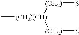
- The fluorine atoms of the RA-subgroup may influence the bond between the mercapto group and the metal. To avoid this it is preferable to use an RS-subgroup containing at least one hydrocarbon unit with the structure:
- —(CH2)—
- The unit —(CH 2)— “isolates” the fluorine atoms of the RA-subgroup from the bond. Preferably an alkyl-group with at least 2-3 units of this type should be used for best “isolation” of the RA-subgroup from the mercapto-group. The shortest RS-subgroup is thus preferably:
- —(CH2)(CH2)—
- For reasons of close packing of the RX-compound the RS-subgroup is preferably a linear group, such as for example
- —(CH2)(CH2)(CH2)— [linear chain, no branches]
- or a group with short branches such as for example

- [main chain with one branch]
- or

- [main chain with one branch at each end]
- The branches, if any, preferably have a length of 1-3 carbon atoms each. Preferably the RS-subgroup is an alkyl-group. In the case of a branched RS-subgroup several RA-subgroups and/or several mercapto groups may be attached to the RS-subgroup. RA- and RS-subgroups containing double or tripple bonds are possible but less preferred since they may participate in unwanted addition reactions during heating of the mold.
- The mold used in the nano-imprint process is a metal mold. The metal mold may be of two different types. The first type is a mold made from solid metal. The nano structure is formed directly on the metal surface by e.g. an etching process known in the art. The second type is a mold comprising a base, e.g. made from silicon. The base may be solid or made from several layers, and may be provided with a surface layer or film that is made from a metal. A preferred embodiment of this second type of mold is to first form the nano structure on a silicon surface, by e.g. etching processes known in the art. Then a very thin layer of metal is applied on top of the silicon surface using e.g. thermic evaporation or electrochemical precipitation. The thickness of the metal layer depenas on the nano structure and the required wear resistance of the mold. In this way a mold is obtained having a metal surface that has a well defined nano structure and good wear properties.
- Several different metals, such as nickel, chromium, titanium, platinum, copper, silver, and gold, may be used for the mold. The preferred metals are nickel, Ni, and chromium, Cr, due to their corrosion resistance, moderate price and high hardness. An important aspect is that the non-sticking layer on the metal mold should have very uniform properties. The binding process and the binding energy of the monomolecular non-sticking layer will be different for different metals. The metal surface is thus preferably a rather pure metal, such as unalloyed nickel or unalloyed chromium. Alloys, such as stainless steel, and mixtures, such as a mixture of e.g. chromium and nickel, are less preferred, since the properties of the monomolecular non-sticking layer bound to an alloy or a mixture will vary over the surface.
- The X-group binds the RX-compound to the surface of the metal mold. The X-group includes at least one mercapto group. One such mercapto group is the SH unit, wherein S denotes sulfur and H denotes hydrogen. The sulfur atom is bound directly to one of the carbon atoms of the R-group. If an RS-subgroup is included, then the sulfur of the SH unit is bound to one of the carbon atoms in that subgroup. If no RS-subgroup is present then the sulfur is bound to one of the carbon atoms in the RA-subgroup. The X-group may contain more than one SH unit, for example 2-4 SH units. In that case each SH-unit is bound to one carbon atom. The RS-subgroup bound to a X-group may, for example, have the following structure:
- —(CH2)(CH2)SH [RS-subgroup with X-group being one SH-unit]
- or

- [branched RS-subgroup with X-group being two SH units]
- The SH units may, if they have a number of 2-4 in each molecule of the RX-compound, form internal sulfur bridges, that is an S-S unit, such as for example:
- [branched RS-subgroup with X-group being a S-S unit]
- The S-S unit is also included under the definition mercapto group, since the S-S unit reacts with metal surfaces in exactly the same way as the SH units and is basically just another state of SH units.
- The mercapto groups react readily with the metals to form metal sulfides, such as nickel sulfide or chromium sulfide. An RX-compound, where X includes two or more SH units or at least one S-S unit, provides a stronger attachment of the RX-compound to the surface. This is preferred in cases where each metal sulfide bond is weak or when an extra strong attachment is required. An example of such an attachment, using a molecule with two SH units or a molecule with a sulfur bridge, that is an S-S unit, is shown below:

- [branched RS-subgroup with X-group being two SH units or one S-S unit after attachment to a nickel surface]
- For extremely small nano structures very small RX-compounds may be preferable. The main chain of the R-group may then be as short as 2-3 carbon atoms. Examples of such RX-compounds, with R-groups having in total only 2-5 carbon atoms include:
- (CF3)(CH2)SH [linear R-group having two carbon atoms]
- and

- [R-group with main chain having one branch]
- The conditions during the reaction between the metal surface and the RX-compound are such that the compound is in a gaseous phase or in a liquid phase while the mold is in a solid phase.
- For reactions with the RX-compound in a gaseous phase it is preferred to clean the mold and place it in a vacuum oven under low pressure (about 10-200 mbar, preferably about 50-100 mbar) and at a temperature of about 50-200° C., preferably about 70-120° C. The fluoroalkyl compound having a mercapto group (the RX-compound) is then introduced into the oven. The mercapto group reacts with the metal surface forming a metal sulfide. When the reaction is completed the mold is withdrawn from the oven, cleaned, allowed to cool down and is then ready for use.
- For reactions with the RX-compound in a liquid phase the mold is preferably cleaned in a solvent being adapted to the RX-compound. Examples of such a solvent include alkanes like pentane, hexane, heptane, octane etc. A solution is prepared by dissolving the RX-compound in a solvent, preferably the same solvent as was used for cleaning the mold. The concentration of the RX-compound in the solution is not critical, but often 1-10% is convenient. The temperature of the solution is not critical, but for practical reasons room temperature is often convenient. The cleaned mold is then dipped into an agitated container containing the solution. The mercapto group reacts with the metal surface forming a metal sulfide. The mold is then removed from the container and is cleaned by dipping it into one or several consecutive baths each preferably containing the same solvent as was used for the solution. The mold is finally dried, either by heating it sufficiently to evaporate the solvent or by flushing it with nitrogen gas.
- The choice of RX-compounds of the formula above is not critical according to the invention and one skilled in the art can easily, without extensive experimentation, find the most appropriate one in each case. By this choice possibility the layer can be tailored in view of factors material to the actual use of the mold, which is a great advantage.
- Best Mode of Performing the Invention.
- An embodiment of the invention, which at present is judged to be the best mode of performing the invention, will be described below with reference to a working example.
- A silicon mold was etched to define a certain nano structure. The surface of the mold was then coated with a thin layer of nickel. The mold was cleaned in heptane.
- A fluoroalkyl compound having a mercapto group, which compound was 1H, 1H, 2H, 2H-perfluorooctanethiol and had the structure:
- CF3(CF2)5(CH2)2SH
- was dissolved in heptane to obtain a 2% solution. The temperature of the solution was about 20° C. The cleaned metal mold was put into an agitated beaker containing the solution. The mold was now provided with a mono-molecular non-sticking layer with the structure:
- CF3 (CF2)5(CH2)2S—Ni
- The mold was taken up from the beaker and was cleaned by dipping it in each of three consecutive beakers each containing heptane. The mold was then heated to 70° C. whereby the heptane was evaporated. The mold was tested in a nano-imprint lithography process and it was found that the mold withstood more than 50 imprint sequences without any detectable degradation.
- The example above was repeated, except that the following fluoroalkyl compounds having a mercapto group were used:
TABLE 1 Additionally tested compounds R-group RA-subgroup RS-subgroup X-group Metal (CF3)— —(CH2)2— —SH Ni (CF3)2(CF)— —(CH2) (CH) ((CH2)—)2 —S—S— Cr (CF3) (CF2)3— —(CH2)2— —SH Ni (CF3) (CF2)7— —(CH2)2— —SH Cr - Similar results were obtained upon testing.
- The same RX-compound as described in example 1 was applied to a mold similar to that used in example 1. The mold was cleaned in heptane and then put into an oven that had a temperature of 110° C., a nitrogen atmosphere and a pressure of 75 mbar. Pure RX-compound was injected into the oven. The mold, now provided with a mono-molecular non-sticking layer with a structure similar to that described in example 1, was taken out of the oven and was cleaned by dipping it in each of three consecutive beakers each containing heptane. Finally, the mold was dried by heating it to 70° C. Similar results as in example 1 were obtained upon testing.
Claims (12)
1. A metal mold for use in a nano-imprinting process comprising a firmly adhering monomolecular non-sticking layer, said layer being obtained by subjecting the mold to a reaction with a fluoroalkyl compound having a mercapto group, said layer, as a result of said reaction, comprising a sulfide of said metal.
2. A metal mold as claimed in claim 1 , wherein the mold is made of solid metal or has a metal surface.
3. A metal mold as claimed in claim 2 , wherein the metal mold comprises a thin layer of metal applied on a base material.
4. A metal mold as claimed in any of claims 1-3, wherein the metal is nickel or chromium.
5. A metal mold as claimed in any of claims 1-4, wherein the metal is unalloyed.
6. A metal mold as claimed in any of claims 1-5, wherein the fluoroalkyl compound having a mercapto group is denoted RX where;
R is a group with non-sticking properties, and
X includes at least one mercapto group,
wherein r is a linear fluoroalkyl group, which has a first end and a second end and which has no or only short branches, and wherein r at the first end includes at least one fluorinated carbon atom and at the second end is bound to X.
7. A metal mold as claimed in claim 6 , wherein at least one of said at least one fluorinated carbon atom is a perfluorinated carbon atom.
8. A metal mold as claimed in any of claims 6-7, wherein R is a linear main chain, wherein the first end of R includes 1-3 branches, each with a length of 1-3 carbon atoms, and wherein each of the branches and the first end of R includes a perfluorinated carbon atom.
9. A metal mold as claimed in any of claims 6-7, wherein the main chain of R has a total length of 2-3 carbon atoms.
10. A metal mold as claimed in any of claims 1-9, wherein the nano-imprinting process is nano-imprint lithography.
11. A metal mold as claimed in any of claims 1-10, wherein during said reaction the fluoroalkyl compound is in a gaseous phase.
12. A metal mold as claimed in any of claims 1-10, wherein during said reaction the fluoroalkyl compound is in a liquid phase or is dissolved in a solvent.
Priority Applications (1)
| Application Number | Priority Date | Filing Date | Title |
|---|---|---|---|
| US10/181,487 US6923930B2 (en) | 2000-01-21 | 2001-01-19 | Mold for nano imprinting |
Applications Claiming Priority (5)
| Application Number | Priority Date | Filing Date | Title |
|---|---|---|---|
| US17728400P | 2000-01-21 | 2000-01-21 | |
| SE0000173A SE517093C2 (en) | 2000-01-21 | 2000-01-21 | Metal mold for use in nano-imprint lithography, comprises monomolecular non-sticking layer obtained by subjecting mold to reaction with fluoroalkyl compound having mercapto group |
| SE0000173-5 | 2000-01-21 | ||
| US10/181,487 US6923930B2 (en) | 2000-01-21 | 2001-01-19 | Mold for nano imprinting |
| PCT/SE2001/000087 WO2001053889A1 (en) | 2000-01-21 | 2001-01-19 | A mold for nano imprinting |
Publications (2)
| Publication Number | Publication Date |
|---|---|
| US20030127580A1 true US20030127580A1 (en) | 2003-07-10 |
| US6923930B2 US6923930B2 (en) | 2005-08-02 |
Family
ID=26654958
Family Applications (1)
| Application Number | Title | Priority Date | Filing Date |
|---|---|---|---|
| US10/181,487 Expired - Lifetime US6923930B2 (en) | 2000-01-21 | 2001-01-19 | Mold for nano imprinting |
Country Status (6)
| Country | Link |
|---|---|
| US (1) | US6923930B2 (en) |
| EP (1) | EP1257878B1 (en) |
| AT (1) | ATE332517T1 (en) |
| AU (1) | AU2001228987A1 (en) |
| DE (1) | DE60121302T2 (en) |
| WO (1) | WO2001053889A1 (en) |
Cited By (31)
| Publication number | Priority date | Publication date | Assignee | Title |
|---|---|---|---|---|
| EP1533657A1 (en) * | 2003-11-21 | 2005-05-25 | Obducat AB | Multilayer nano imprint lithography |
| WO2005068694A1 (en) * | 2004-01-19 | 2005-07-28 | Maschinenfabrik Rieter Ag | Nonwoven guide device for a comber |
| US20050193944A1 (en) * | 2004-03-04 | 2005-09-08 | Asml Netherlands B.V. | Printing apparatus and device manufacturing method |
| US20050272599A1 (en) * | 2004-06-04 | 2005-12-08 | Kenneth Kramer | Mold release layer |
| US20060137555A1 (en) * | 2004-12-23 | 2006-06-29 | Asml Netherlands B.V. | Imprint lithography |
| US20060144275A1 (en) * | 2004-12-30 | 2006-07-06 | Asml Netherlands B.V. | Imprint lithography |
| US20060144814A1 (en) * | 2004-12-30 | 2006-07-06 | Asml Netherlands B.V. | Imprint lithography |
| US20060144274A1 (en) * | 2004-12-30 | 2006-07-06 | Asml Netherlands B.V. | Imprint lithography |
| US20060150849A1 (en) * | 2004-12-30 | 2006-07-13 | Asml Netherlands B.V. | Imprint lithography |
| US20060154179A1 (en) * | 2005-01-07 | 2006-07-13 | Asml Netherlands B. V. | Imprint lithography |
| US20060180952A1 (en) * | 2005-02-17 | 2006-08-17 | Asml Netherlands B.V. | Imprint lithography |
| US20060196377A1 (en) * | 2005-03-07 | 2006-09-07 | Asml Netherlands B.V. | Imprint lithography |
| US20060230959A1 (en) * | 2005-04-19 | 2006-10-19 | Asml Netherlands B.V. | Imprint lithography |
| US20060231979A1 (en) * | 2005-04-19 | 2006-10-19 | Asml Netherlands B.V. | Imprint lithography |
| US20060254446A1 (en) * | 2005-05-16 | 2006-11-16 | Asml Netherlands B.V. | Imprint lithography |
| US20060255505A1 (en) * | 2005-05-11 | 2006-11-16 | Micron Technology, Inc. | Imprint templates for imprint lithography, and methods of patterning a plurality of substrates |
| US20060267231A1 (en) * | 2005-05-27 | 2006-11-30 | Asml Netherlands B.V. | Imprint lithography |
| US20060266244A1 (en) * | 2005-05-31 | 2006-11-30 | Asml Netherlands B.V. | Imprint lithography |
| US20060268256A1 (en) * | 2005-05-27 | 2006-11-30 | Asml Netherlands B.V. | Imprint lithography |
| US20060280829A1 (en) * | 2005-06-13 | 2006-12-14 | Asml Netherlands B.V. | Imprint lithography |
| US20070018360A1 (en) * | 2005-07-21 | 2007-01-25 | Asml Netherlands B.V. | Imprint lithography |
| US20070023976A1 (en) * | 2005-07-26 | 2007-02-01 | Asml Netherlands B.V. | Imprint lithography |
| US20070102838A1 (en) * | 2005-11-04 | 2007-05-10 | Asml Netherlands B.V. | Imprint lithography |
| US20070102844A1 (en) * | 2005-11-04 | 2007-05-10 | Asml Netherlands B.V. | Imprint lithography |
| US20070141191A1 (en) * | 2005-12-21 | 2007-06-21 | Asml Netherlands B.V. | Imprint lithography |
| US20070138699A1 (en) * | 2005-12-21 | 2007-06-21 | Asml Netherlands B.V. | Imprint lithography |
| US20080003827A1 (en) * | 2006-06-30 | 2008-01-03 | Asml Netherlands B.V. | Imprintable medium dispenser |
| US20080011934A1 (en) * | 2006-06-30 | 2008-01-17 | Asml Netherlands B.V. | Imprint lithography |
| US20090038636A1 (en) * | 2007-08-09 | 2009-02-12 | Asml Netherlands B.V. | Cleaning method |
| US20090057267A1 (en) * | 2007-09-05 | 2009-03-05 | Asml Netherlands B.V. | Imprint lithography |
| US7854877B2 (en) | 2007-08-14 | 2010-12-21 | Asml Netherlands B.V. | Lithography meandering order |
Families Citing this family (29)
| Publication number | Priority date | Publication date | Assignee | Title |
|---|---|---|---|---|
| EP2270592B1 (en) | 2000-07-17 | 2015-09-02 | Board of Regents, The University of Texas System | Method of forming a pattern on a substrate |
| JP2004523906A (en) | 2000-10-12 | 2004-08-05 | ボード・オブ・リージエンツ,ザ・ユニバーシテイ・オブ・テキサス・システム | Templates for room-temperature and low-pressure micro and nano-transfer lithography |
| SE519573C2 (en) * | 2001-07-05 | 2003-03-11 | Obducat Ab | Stamp with anti-adhesive layer as well as ways of making and ways to repair such a stamp |
| US7037639B2 (en) | 2002-05-01 | 2006-05-02 | Molecular Imprints, Inc. | Methods of manufacturing a lithography template |
| CN100341712C (en) * | 2002-06-20 | 2007-10-10 | 奥博杜卡特股份公司 | Mold tool method of manufacturing a mold tool and storage medium formed by use of the mold tool |
| WO2004045858A1 (en) * | 2002-11-21 | 2004-06-03 | Council Of Scientific And Industrial Research | Colored nanolithography on glass and plastic substrates |
| ATE551383T1 (en) | 2003-09-23 | 2012-04-15 | Univ North Carolina | PHOTOHARDENABLE PERFLUORUM POLYETHERS FOR USE AS NEW MATERIALS IN MICROFLUIDIC DEVICES |
| CA2847260C (en) | 2003-12-19 | 2016-06-21 | The University Of North Carolina At Chapel Hill | Methods for fabricating isolated micro- and nano- structures using soft or imprint lithography |
| US9040090B2 (en) | 2003-12-19 | 2015-05-26 | The University Of North Carolina At Chapel Hill | Isolated and fixed micro and nano structures and methods thereof |
| KR100595515B1 (en) * | 2003-12-31 | 2006-07-03 | 엘지전자 주식회사 | Micro-structure patterned mold and a method for coating monolayer release therein |
| AU2005220150A1 (en) * | 2004-02-13 | 2005-09-15 | The University Of North Carolina At Chapel Hill | Functional materials and novel methods for the fabrication of microfluidic devices |
| WO2007021762A2 (en) | 2005-08-09 | 2007-02-22 | The University Of North Carolina At Chapel Hill | Methods and materials for fabricating microfluidic devices |
| EP1600811A1 (en) * | 2004-05-28 | 2005-11-30 | Obducat AB | Modified metal molds for use in imprinting processes |
| US7717693B2 (en) * | 2004-05-28 | 2010-05-18 | Obducat Ab | Modified metal mold for use in imprinting processes |
| JP2005353725A (en) * | 2004-06-09 | 2005-12-22 | Shinko Electric Ind Co Ltd | Method for forming active element on substrate, and substrate |
| TWI240328B (en) * | 2004-08-27 | 2005-09-21 | Univ Nat Cheng Kung | Pretreatment process of substrate in micro-nano imprinting technology |
| EP1853967A4 (en) * | 2005-02-03 | 2009-11-11 | Univ North Carolina | Low surface energy polymeric material for use in liquid crystal displays |
| WO2007133235A2 (en) * | 2005-08-08 | 2007-11-22 | Liquidia Technologies, Inc. | Micro and nano-structure metrology |
| KR100693992B1 (en) | 2005-08-20 | 2007-03-12 | 이헌 | Nickel stamp structure for providing easy formation of self-assembled monolayer as anti-stiction layer, and manufacturing method thereof |
| US7388661B2 (en) * | 2006-10-20 | 2008-06-17 | Hewlett-Packard Development Company, L.P. | Nanoscale structures, systems, and methods for use in nano-enhanced raman spectroscopy (NERS) |
| US7391511B1 (en) | 2007-01-31 | 2008-06-24 | Hewlett-Packard Development Company, L.P. | Raman signal-enhancing structures and Raman spectroscopy systems including such structures |
| US20100151031A1 (en) * | 2007-03-23 | 2010-06-17 | Desimone Joseph M | Discrete size and shape specific organic nanoparticles designed to elicit an immune response |
| JP5456465B2 (en) * | 2007-06-04 | 2014-03-26 | 丸善石油化学株式会社 | Finely processed product and manufacturing method thereof |
| US20090041986A1 (en) * | 2007-06-21 | 2009-02-12 | 3M Innovative Properties Company | Method of making hierarchical articles |
| US20090114618A1 (en) * | 2007-06-21 | 2009-05-07 | 3M Innovative Properties Company | Method of making hierarchical articles |
| US20080315459A1 (en) * | 2007-06-21 | 2008-12-25 | 3M Innovative Properties Company | Articles and methods for replication of microstructures and nanofeatures |
| JP5871907B2 (en) | 2010-04-28 | 2016-03-01 | キンバリー クラーク ワールドワイド インコーポレイテッド | Nanopatterned medical device with enhanced cell-cell interaction |
| US8945688B2 (en) | 2011-01-03 | 2015-02-03 | General Electric Company | Process of forming a material having nano-particles and a material having nano-particles |
| JP6535464B2 (en) | 2011-10-27 | 2019-06-26 | ソレント・セラピューティクス・インコーポレイテッド | Implantable device for delivery of bioactive agents |
Citations (8)
| Publication number | Priority date | Publication date | Assignee | Title |
|---|---|---|---|---|
| US4584156A (en) * | 1984-06-18 | 1986-04-22 | U.S. Philips Corporation | Mold and method of manufacturing polyurethane products |
| US5259926A (en) * | 1991-09-24 | 1993-11-09 | Hitachi, Ltd. | Method of manufacturing a thin-film pattern on a substrate |
| US5358604A (en) * | 1992-09-29 | 1994-10-25 | Microelectronics And Computer Technology Corp. | Method for producing conductive patterns |
| US5512131A (en) * | 1993-10-04 | 1996-04-30 | President And Fellows Of Harvard College | Formation of microstamped patterns on surfaces and derivative articles |
| US5772905A (en) * | 1995-11-15 | 1998-06-30 | Regents Of The University Of Minnesota | Nanoimprint lithography |
| US6656398B2 (en) * | 2001-06-19 | 2003-12-02 | Corning Incorporated | Process of making a pattern in a film |
| US6743368B2 (en) * | 2002-01-31 | 2004-06-01 | Hewlett-Packard Development Company, L.P. | Nano-size imprinting stamp using spacer technique |
| US6829988B2 (en) * | 2003-05-16 | 2004-12-14 | Suss Microtec, Inc. | Nanoimprinting apparatus and method |
Family Cites Families (2)
| Publication number | Priority date | Publication date | Assignee | Title |
|---|---|---|---|---|
| US6309580B1 (en) | 1995-11-15 | 2001-10-30 | Regents Of The University Of Minnesota | Release surfaces, particularly for use in nanoimprint lithography |
| DE19815130A1 (en) | 1998-04-03 | 1999-10-14 | Bosch Gmbh Robert | Electroformed metal stamp, for defining nanostructures, is produced |
-
2001
- 2001-01-19 DE DE60121302T patent/DE60121302T2/en not_active Expired - Lifetime
- 2001-01-19 AT AT01942726T patent/ATE332517T1/en active
- 2001-01-19 AU AU2001228987A patent/AU2001228987A1/en not_active Abandoned
- 2001-01-19 WO PCT/SE2001/000087 patent/WO2001053889A1/en active IP Right Grant
- 2001-01-19 EP EP01942726A patent/EP1257878B1/en not_active Expired - Lifetime
- 2001-01-19 US US10/181,487 patent/US6923930B2/en not_active Expired - Lifetime
Patent Citations (8)
| Publication number | Priority date | Publication date | Assignee | Title |
|---|---|---|---|---|
| US4584156A (en) * | 1984-06-18 | 1986-04-22 | U.S. Philips Corporation | Mold and method of manufacturing polyurethane products |
| US5259926A (en) * | 1991-09-24 | 1993-11-09 | Hitachi, Ltd. | Method of manufacturing a thin-film pattern on a substrate |
| US5358604A (en) * | 1992-09-29 | 1994-10-25 | Microelectronics And Computer Technology Corp. | Method for producing conductive patterns |
| US5512131A (en) * | 1993-10-04 | 1996-04-30 | President And Fellows Of Harvard College | Formation of microstamped patterns on surfaces and derivative articles |
| US5772905A (en) * | 1995-11-15 | 1998-06-30 | Regents Of The University Of Minnesota | Nanoimprint lithography |
| US6656398B2 (en) * | 2001-06-19 | 2003-12-02 | Corning Incorporated | Process of making a pattern in a film |
| US6743368B2 (en) * | 2002-01-31 | 2004-06-01 | Hewlett-Packard Development Company, L.P. | Nano-size imprinting stamp using spacer technique |
| US6829988B2 (en) * | 2003-05-16 | 2004-12-14 | Suss Microtec, Inc. | Nanoimprinting apparatus and method |
Cited By (79)
| Publication number | Priority date | Publication date | Assignee | Title |
|---|---|---|---|---|
| US20080138460A1 (en) * | 2003-11-21 | 2008-06-12 | Obducat Ab | Multilayer nano imprint lithography |
| EP1533657A1 (en) * | 2003-11-21 | 2005-05-25 | Obducat AB | Multilayer nano imprint lithography |
| CN100554538C (en) * | 2004-01-19 | 2009-10-28 | 里特机械公司 | Combing machine web guiding device |
| WO2005068694A1 (en) * | 2004-01-19 | 2005-07-28 | Maschinenfabrik Rieter Ag | Nonwoven guide device for a comber |
| US7730834B2 (en) | 2004-03-04 | 2010-06-08 | Asml Netherlands B.V. | Printing apparatus and device manufacturing method |
| US7698999B2 (en) | 2004-03-04 | 2010-04-20 | Asml Netherlands B.V. | Printing apparatus and device manufacturing method |
| US20050193944A1 (en) * | 2004-03-04 | 2005-09-08 | Asml Netherlands B.V. | Printing apparatus and device manufacturing method |
| US20050211161A1 (en) * | 2004-03-04 | 2005-09-29 | Asml Netherlands B.V. | Printing apparatus and device manufacturing method |
| US20050272599A1 (en) * | 2004-06-04 | 2005-12-08 | Kenneth Kramer | Mold release layer |
| US7676088B2 (en) | 2004-12-23 | 2010-03-09 | Asml Netherlands B.V. | Imprint lithography |
| US8571318B2 (en) | 2004-12-23 | 2013-10-29 | Asml Netherlands B.V. | Imprint lithography |
| US20060159305A1 (en) * | 2004-12-23 | 2006-07-20 | Asml Netherlands B.V. | Imprint lithography |
| US20060137555A1 (en) * | 2004-12-23 | 2006-06-29 | Asml Netherlands B.V. | Imprint lithography |
| US7636475B2 (en) | 2004-12-23 | 2009-12-22 | Asml Netherlands B.V. | Imprint lithography |
| US8131078B2 (en) | 2004-12-23 | 2012-03-06 | Asml Netherlands B.V. | Imprint lithography |
| US20100050893A1 (en) * | 2004-12-23 | 2010-03-04 | Asml Netherlands B.V. | Imprint lithography |
| US20100139862A1 (en) * | 2004-12-30 | 2010-06-10 | Asml Netherlands B.V. | Imprint lithography |
| US7686970B2 (en) | 2004-12-30 | 2010-03-30 | Asml Netherlands B.V. | Imprint lithography |
| US20060144274A1 (en) * | 2004-12-30 | 2006-07-06 | Asml Netherlands B.V. | Imprint lithography |
| US20060150849A1 (en) * | 2004-12-30 | 2006-07-13 | Asml Netherlands B.V. | Imprint lithography |
| US20060144814A1 (en) * | 2004-12-30 | 2006-07-06 | Asml Netherlands B.V. | Imprint lithography |
| US7490547B2 (en) | 2004-12-30 | 2009-02-17 | Asml Netherlands B.V. | Imprint lithography |
| US20060144275A1 (en) * | 2004-12-30 | 2006-07-06 | Asml Netherlands B.V. | Imprint lithography |
| US9341944B2 (en) | 2004-12-30 | 2016-05-17 | Asml Netherlands B.V. | Imprint lithography |
| US20060154179A1 (en) * | 2005-01-07 | 2006-07-13 | Asml Netherlands B. V. | Imprint lithography |
| US7354698B2 (en) | 2005-01-07 | 2008-04-08 | Asml Netherlands B.V. | Imprint lithography |
| US20060180952A1 (en) * | 2005-02-17 | 2006-08-17 | Asml Netherlands B.V. | Imprint lithography |
| US7922474B2 (en) | 2005-02-17 | 2011-04-12 | Asml Netherlands B.V. | Imprint lithography |
| US20060196377A1 (en) * | 2005-03-07 | 2006-09-07 | Asml Netherlands B.V. | Imprint lithography |
| US7906059B2 (en) | 2005-03-07 | 2011-03-15 | Asml Netherlands B.V. | Imprint lithography |
| US7523701B2 (en) | 2005-03-07 | 2009-04-28 | Asml Netherlands B.V. | Imprint lithography method and apparatus |
| US7762186B2 (en) | 2005-04-19 | 2010-07-27 | Asml Netherlands B.V. | Imprint lithography |
| US8349238B2 (en) | 2005-04-19 | 2013-01-08 | Asml Netherlands B.V. | Imprint lithography |
| US20060230959A1 (en) * | 2005-04-19 | 2006-10-19 | Asml Netherlands B.V. | Imprint lithography |
| US20060231979A1 (en) * | 2005-04-19 | 2006-10-19 | Asml Netherlands B.V. | Imprint lithography |
| US7611348B2 (en) | 2005-04-19 | 2009-11-03 | Asml Netherlands B.V. | Imprint lithography |
| US20060255505A1 (en) * | 2005-05-11 | 2006-11-16 | Micron Technology, Inc. | Imprint templates for imprint lithography, and methods of patterning a plurality of substrates |
| US7767129B2 (en) | 2005-05-11 | 2010-08-03 | Micron Technology, Inc. | Imprint templates for imprint lithography, and methods of patterning a plurality of substrates |
| US7931844B2 (en) | 2005-05-16 | 2011-04-26 | Asml Netherlands B.V. | Imprint lithography |
| US20060254446A1 (en) * | 2005-05-16 | 2006-11-16 | Asml Netherlands B.V. | Imprint lithography |
| US7442029B2 (en) | 2005-05-16 | 2008-10-28 | Asml Netherlands B.V. | Imprint lithography |
| US7692771B2 (en) | 2005-05-27 | 2010-04-06 | Asml Netherlands B.V. | Imprint lithography |
| US20060275524A1 (en) * | 2005-05-27 | 2006-12-07 | Asml Netherlands B.V. | Imprint lithography |
| US20100084565A1 (en) * | 2005-05-27 | 2010-04-08 | Asml Netherlands B.V. | Imprint lithography |
| US7618250B2 (en) | 2005-05-27 | 2009-11-17 | Asml Netherlands B.V. | Imprint lithography |
| US20060268256A1 (en) * | 2005-05-27 | 2006-11-30 | Asml Netherlands B.V. | Imprint lithography |
| US20060267231A1 (en) * | 2005-05-27 | 2006-11-30 | Asml Netherlands B.V. | Imprint lithography |
| US8241550B2 (en) | 2005-05-27 | 2012-08-14 | Asml Netherlands B.V. | Imprint lithography |
| US20060266244A1 (en) * | 2005-05-31 | 2006-11-30 | Asml Netherlands B.V. | Imprint lithography |
| US7418902B2 (en) | 2005-05-31 | 2008-09-02 | Asml Netherlands B.V. | Imprint lithography including alignment |
| US20060280829A1 (en) * | 2005-06-13 | 2006-12-14 | Asml Netherlands B.V. | Imprint lithography |
| US7377764B2 (en) | 2005-06-13 | 2008-05-27 | Asml Netherlands B.V. | Imprint lithography |
| US7708924B2 (en) | 2005-07-21 | 2010-05-04 | Asml Netherlands B.V. | Imprint lithography |
| US20070018360A1 (en) * | 2005-07-21 | 2007-01-25 | Asml Netherlands B.V. | Imprint lithography |
| US20070023976A1 (en) * | 2005-07-26 | 2007-02-01 | Asml Netherlands B.V. | Imprint lithography |
| US7878791B2 (en) | 2005-11-04 | 2011-02-01 | Asml Netherlands B.V. | Imprint lithography |
| US8011915B2 (en) | 2005-11-04 | 2011-09-06 | Asml Netherlands B.V. | Imprint lithography |
| US10025206B2 (en) | 2005-11-04 | 2018-07-17 | Asml Netherlands B.V. | Imprint lithography |
| US20070102844A1 (en) * | 2005-11-04 | 2007-05-10 | Asml Netherlands B.V. | Imprint lithography |
| US9864271B2 (en) | 2005-11-04 | 2018-01-09 | Asml Netherlands B.V. | Imprint lithography |
| US9778563B2 (en) | 2005-11-04 | 2017-10-03 | Asml Netherlands B.V. | Imprint lithography |
| US20070102838A1 (en) * | 2005-11-04 | 2007-05-10 | Asml Netherlands B.V. | Imprint lithography |
| US20070141191A1 (en) * | 2005-12-21 | 2007-06-21 | Asml Netherlands B.V. | Imprint lithography |
| US9610727B2 (en) | 2005-12-21 | 2017-04-04 | Asml Netherlands B.V. | Imprint lithography |
| US8100684B2 (en) | 2005-12-21 | 2012-01-24 | Asml Netherlands B.V. | Imprint lithography |
| US8753557B2 (en) | 2005-12-21 | 2014-06-17 | Asml Netherlands B.V. | Imprint lithography |
| US7517211B2 (en) | 2005-12-21 | 2009-04-14 | Asml Netherlands B.V. | Imprint lithography |
| US20070138699A1 (en) * | 2005-12-21 | 2007-06-21 | Asml Netherlands B.V. | Imprint lithography |
| US20090212462A1 (en) * | 2005-12-21 | 2009-08-27 | Asml Netherlans B.V. | Imprint lithography |
| US8486485B2 (en) | 2006-06-30 | 2013-07-16 | Asml Netherlands B.V. | Method of dispensing imprintable medium |
| US8318253B2 (en) | 2006-06-30 | 2012-11-27 | Asml Netherlands B.V. | Imprint lithography |
| US20080003827A1 (en) * | 2006-06-30 | 2008-01-03 | Asml Netherlands B.V. | Imprintable medium dispenser |
| US8015939B2 (en) | 2006-06-30 | 2011-09-13 | Asml Netherlands B.V. | Imprintable medium dispenser |
| US20080011934A1 (en) * | 2006-06-30 | 2008-01-17 | Asml Netherlands B.V. | Imprint lithography |
| US20090038636A1 (en) * | 2007-08-09 | 2009-02-12 | Asml Netherlands B.V. | Cleaning method |
| US7854877B2 (en) | 2007-08-14 | 2010-12-21 | Asml Netherlands B.V. | Lithography meandering order |
| US8323541B2 (en) | 2007-09-05 | 2012-12-04 | Asml Netherlands B.V. | Imprint lithography |
| US8144309B2 (en) | 2007-09-05 | 2012-03-27 | Asml Netherlands B.V. | Imprint lithography |
| US20090057267A1 (en) * | 2007-09-05 | 2009-03-05 | Asml Netherlands B.V. | Imprint lithography |
Also Published As
| Publication number | Publication date |
|---|---|
| WO2001053889A1 (en) | 2001-07-26 |
| EP1257878A1 (en) | 2002-11-20 |
| DE60121302D1 (en) | 2006-08-17 |
| US6923930B2 (en) | 2005-08-02 |
| AU2001228987A1 (en) | 2001-07-31 |
| DE60121302T2 (en) | 2007-06-28 |
| EP1257878B1 (en) | 2006-07-05 |
| ATE332517T1 (en) | 2006-07-15 |
Similar Documents
| Publication | Publication Date | Title |
|---|---|---|
| US6923930B2 (en) | Mold for nano imprinting | |
| US20050287820A1 (en) | Mold for nano imprinting | |
| EP1759245B1 (en) | Modified metal mold for use in imprinting processes | |
| Wagner et al. | Formation and in situ modification of monolayers chemisorbed on ultraflat template-stripped gold surfaces | |
| US7448860B2 (en) | Surface modified stamper for imprint lithography | |
| Lewis et al. | Control and placement of molecules via self-assembly | |
| Hirai et al. | Nano-imprint lithography using replicated mold by Ni electroforming | |
| KR20090117699A (en) | Imprint mold and method for production thereof | |
| KR100693992B1 (en) | Nickel stamp structure for providing easy formation of self-assembled monolayer as anti-stiction layer, and manufacturing method thereof | |
| US20080224358A1 (en) | Nano-Molding Process | |
| Nakamatsu et al. | Fluorinated diamond-like carbon coating as antisticking layer on nanoimprint mold | |
| Cheung et al. | Chemical lift-off lithography of metal and semiconductor surfaces | |
| Sato et al. | A study of topographic effects on chemical force microscopy using adhesive force mapping | |
| Miikkulainen et al. | Thin films of MoN, WN, and perfluorinated silane deposited from dimethylamido precursors as contamination resistant coatings on micro-injection mold inserts | |
| Wu et al. | Anti-adhesive effects of diverse self-assembled monolayers in nanoimprint lithography | |
| Kankate et al. | Vapor phase exchange of self-assembled monolayers for engineering of biofunctional surfaces | |
| KR20130023366A (en) | Metal mold for use in imprinting processes | |
| Yamada et al. | Surface evaluation of fluorinated diamond-like carbon thin film as an antisticking layer of nanoimprint mold | |
| Beck et al. | Improving nanoimprint lithography stamps for the 10 nm features | |
| Shen et al. | Efficient fabrication process for metallic structures of submicrometer size | |
| Lee | Development of Bidentate Phosphonic Acid Based Self-Assembled Monolayers on Silver | |
| Pan et al. | Investigation of the anti-adhesion layers for nanoimprint molding | |
| Sato et al. | A Study of Nanocontact Printing Using Adhesive Force Mapping | |
| Tormen | Microcontact printing techniques | |
| Enriquez | Nano-Engineering of Molecular Films by Self-Assembly and Langmuir-Blodgett Techniques |
Legal Events
| Date | Code | Title | Description |
|---|---|---|---|
| AS | Assignment |
Owner name: OBDUCAT AKTIEBOLAG, SWEDEN Free format text: ASSIGNMENT OF ASSIGNORS INTEREST;ASSIGNORS:LING, TORBJORN;MONTELIUS, LARS;HEIDARI, BABAK;REEL/FRAME:013368/0591 Effective date: 20020903 |
|
| STCF | Information on status: patent grant |
Free format text: PATENTED CASE |
|
| CC | Certificate of correction | ||
| FPAY | Fee payment |
Year of fee payment: 4 |
|
| FPAY | Fee payment |
Year of fee payment: 8 |
|
| FPAY | Fee payment |
Year of fee payment: 12 |