US20030190786A1 - Memory manufacturing process with bitline isolation - Google Patents
Memory manufacturing process with bitline isolation Download PDFInfo
- Publication number
- US20030190786A1 US20030190786A1 US10/118,732 US11873202A US2003190786A1 US 20030190786 A1 US20030190786 A1 US 20030190786A1 US 11873202 A US11873202 A US 11873202A US 2003190786 A1 US2003190786 A1 US 2003190786A1
- Authority
- US
- United States
- Prior art keywords
- gate
- implanting
- wordline
- dopant
- integrated circuit
- Prior art date
- Legal status (The legal status is an assumption and is not a legal conclusion. Google has not performed a legal analysis and makes no representation as to the accuracy of the status listed.)
- Granted
Links
Images


Classifications
-
- H—ELECTRICITY
- H10—SEMICONDUCTOR DEVICES; ELECTRIC SOLID-STATE DEVICES NOT OTHERWISE PROVIDED FOR
- H10B—ELECTRONIC MEMORY DEVICES
- H10B43/00—EEPROM devices comprising charge-trapping gate insulators
- H10B43/30—EEPROM devices comprising charge-trapping gate insulators characterised by the memory core region
-
- H—ELECTRICITY
- H01—ELECTRIC ELEMENTS
- H01L—SEMICONDUCTOR DEVICES NOT COVERED BY CLASS H10
- H01L21/00—Processes or apparatus adapted for the manufacture or treatment of semiconductor or solid state devices or of parts thereof
- H01L21/02—Manufacture or treatment of semiconductor devices or of parts thereof
- H01L21/04—Manufacture or treatment of semiconductor devices or of parts thereof the devices having at least one potential-jump barrier or surface barrier, e.g. PN junction, depletion layer or carrier concentration layer
- H01L21/18—Manufacture or treatment of semiconductor devices or of parts thereof the devices having at least one potential-jump barrier or surface barrier, e.g. PN junction, depletion layer or carrier concentration layer the devices having semiconductor bodies comprising elements of Group IV of the Periodic System or AIIIBV compounds with or without impurities, e.g. doping materials
- H01L21/26—Bombardment with radiation
- H01L21/263—Bombardment with radiation with high-energy radiation
- H01L21/265—Bombardment with radiation with high-energy radiation producing ion implantation
-
- H—ELECTRICITY
- H01—ELECTRIC ELEMENTS
- H01L—SEMICONDUCTOR DEVICES NOT COVERED BY CLASS H10
- H01L27/00—Devices consisting of a plurality of semiconductor or other solid-state components formed in or on a common substrate
- H01L27/02—Devices consisting of a plurality of semiconductor or other solid-state components formed in or on a common substrate including semiconductor components specially adapted for rectifying, oscillating, amplifying or switching and having at least one potential-jump barrier or surface barrier; including integrated passive circuit elements with at least one potential-jump barrier or surface barrier
- H01L27/04—Devices consisting of a plurality of semiconductor or other solid-state components formed in or on a common substrate including semiconductor components specially adapted for rectifying, oscillating, amplifying or switching and having at least one potential-jump barrier or surface barrier; including integrated passive circuit elements with at least one potential-jump barrier or surface barrier the substrate being a semiconductor body
- H01L27/10—Devices consisting of a plurality of semiconductor or other solid-state components formed in or on a common substrate including semiconductor components specially adapted for rectifying, oscillating, amplifying or switching and having at least one potential-jump barrier or surface barrier; including integrated passive circuit elements with at least one potential-jump barrier or surface barrier the substrate being a semiconductor body including a plurality of individual components in a repetitive configuration
- H01L27/105—Devices consisting of a plurality of semiconductor or other solid-state components formed in or on a common substrate including semiconductor components specially adapted for rectifying, oscillating, amplifying or switching and having at least one potential-jump barrier or surface barrier; including integrated passive circuit elements with at least one potential-jump barrier or surface barrier the substrate being a semiconductor body including a plurality of individual components in a repetitive configuration including field-effect components
-
- H—ELECTRICITY
- H10—SEMICONDUCTOR DEVICES; ELECTRIC SOLID-STATE DEVICES NOT OTHERWISE PROVIDED FOR
- H10B—ELECTRONIC MEMORY DEVICES
- H10B43/00—EEPROM devices comprising charge-trapping gate insulators
- H10B43/40—EEPROM devices comprising charge-trapping gate insulators characterised by the peripheral circuit region
Definitions
- the present invention relates generally to semiconductor technology and more specifically to reducing the number of steps in forming MirrorBit® Flash memory.
- EEPROM electrically erasable programmable read only memory
- EPROM electrically programmable read only memory
- Flash memory A newer type of memory called “Flash” EEPROM, or Flash memory, has become extremely popular because it combines the advantages of the high density and low cost of EPROM with the electrical erasability of EEPROM. Flash memory can be rewritten and can hold its contents without power. It is used in many portable electronic products, such as cell phone, portable computers, voice recorders, etc. as well as in many larger electronic systems, such as cars, planes, industrial control systems, etc.
- Flash memory bits of information are programmed individually as in the older types of memory, such as dynamic random access memory (DRAM) and static random access memory (SRAM) memory chips.
- DRAM dynamic random access memory
- SRAM static random access memory
- Flash memory must currently be erased in fixed multi-bit blocks or sectors.
- Flash memory is constructed of many Flash memory cells where a single bit is stored in each memory cell and the cells are programmed by hot electron injection and erased by Fowler-Nordheim tunneling.
- Flash memory cells have been developed that allow more than a single bit to be stored in each cell.
- One memory cell structure involves the storage of more than one level of charge to be stored in a memory cell with each level representative of a bit.
- This structure is referred to as a multi-level storage (MLS) architecture.
- MLS multi-level storage
- This structure inherently requires a great deal of precision in both programming and reading the differences in the levels to be able to distinguish the bits. If a memory cell using the MLS architecture is overcharged, even by a small amount, the only way to correct the bit error would be to erase the memory cell and totally reprogram the memory cell.
- the need in the MLS architecture to precisely control the amount of charge in a memory cell while programming also makes the technology slower and the data less reliable. It also takes longer to access or “read” precise amounts of charge. Thus, both speed and reliability are sacrificed in order to improve memory cell density.
- MirrorBit® Flash memory An even newer technology allowing multiple bits to be stored in a single cell is known as “MirrorBit®” Flash memory has been developed.
- a memory cell is essentially split into two identical (mirrored) parts, each of which is formulated for storing one of two independent bits.
- Each MirrorBit Flash memory cell like a traditional Flash cell, has a gate with a source and a drain.
- each MirrorBit Flash memory cell can have the connections of the source and drain reversed during operation to permit the storing of two bits.
- the MirrorBit Flash memory cell has a semiconductor substrate with dopant implanted conductive bitlines.
- a multilayer storage layer referred to as a “charge-trapping dielectric layer”, is formed over the semiconductor substrate.
- the charge-trapping dielectric layer can generally be composed of three separate layers: a first insulating layer, a charge-trapping layer, and a second insulating layer.
- Wordlines are formed over the charge-trapping dielectric layer perpendicular to the bitlines.
- Programming circuitry controls two bits per cell by applying a signal to the wordline, which acts as a control gate, and changing bitline connections such that one bit is stored by source and drain being connected in one arrangement and a complementary bit is stored by the source and drain being interchanged in another arrangement.
- the present invention provides a method of manufacturing an integrated circuit with a semiconductor substrate having a core region and a periphery region.
- a charge-trapping dielectric layer is deposited in the core region, and a gate dielectric layer is deposited in the periphery region.
- Bitlines are formed in the semiconductor substrate in the core region and not in the periphery region.
- a wordline-gate layer is formed and implanted with dopant in the core region and not in the periphery region.
- a wordline and a gate are then formed. Source/drain junctions and the gate are implanted with dopant in the periphery region and not in the core region. This method eliminates the problem of the short-circuiting of the buried bitlines because of the difficulty in controlling implant density with smaller devices.
- FIG. 1 is a plan view of a MirrorBit Flash EEPROM according to the present invention
- FIG. 2 is a circuit schematic of a portion of one of the M ⁇ N array cores of FIG. 1;
- FIG. 3 is a plan view of a portion of one of the M ⁇ N array cores and periphery gates of FIG. 1;
- FIG. 4 is a cross-sectional isometric view of a memory cell along the line 4 - 4 of FIG. 3;
- FIG. 5 is a cross-sectional view of a partially processed EEPROM in accordance with the present invention.
- FIG. 6 is the structure of FIG. 5 after deposition of a wordline-gate layer and during a dopant implantation process
- FIG. 7 is the structure of FIG. 6 after formation of the wordlines and the gates;
- FIG. 8 is the structure of FIG. 7 after deposition of a conformal spacer layer
- FIG. 9 is the structure of FIG. 8 after etching of the conformal stop layer
- FIG. 10 is the structure of FIG. 9 during a heavy dopant implantation process.
- FIG. 11 is a simplified flow chart in accordance with the present invention.
- FIG. 1 therein is shown a plan view of a MirrorBit® Flash EEPROM 100 , which commonly includes a semiconductor substrate 102 in which one or more high-density core regions and one or more low-density peripheral portions are formed.
- the EEPROM 100 is manufactured according to the process of the present invention.
- High-density core regions typically include one or more M ⁇ N array cores 104 of individually addressable, substantially identical MirrorBit Flash memory cells.
- Low-density peripheral portions typically include input/output (I/O) circuitry and programming circuitry for selectively addressing the individual memory cells.
- I/O input/output
- the programming circuitry is represented in part by and includes one or more x-decoders 108 and y-decoders 110 , cooperating with I/O circuitry 106 for connecting the source, gate, and drain of selected addressed memory cells to predetermined voltages or impedances to effect designated operations on the memory cell, e.g., programming, reading, and erasing, and deriving necessary voltages to effect such operations.
- horizontal as used in herein is defined as a plane parallel to the conventional plane or surface the semiconductor substrate 102 regardless of its orientation.
- vertical refers to a direction perpendicular to the horizontal as just defined. Terms, such as “on”, “above”, “below”, “higher”, “lower”, “over”, “under”, “thick”, “side” and “beside”, are defined with respect to these horizontal and vertical planes.
- processed and “formed” as used herein is defined to include one or more of the following: depositing or growing semiconductor materials, masking, patterning, photolithography, etching, implanting, removal, and/or stripping.
- FIG. 2 therein is shown a circuit schematic of a portion of one of the M ⁇ N array cores 104 of FIG. 1.
- the circuit schematic shows a line of memory cells 200 , which includes memory cells 201 through 204 and which together can form an 8-bit word.
- Each of the memory cells 201 through 204 is connected to a wordline 206 , which acts as a control gate.
- Each of the memory cells 201 through 204 has two associated bitlines with most of the memory cells having a common bitline.
- the memory cell 201 has associated bitlines 208 and 209 ; the memory cell 202 has associated bitlines 209 and 210 ; the memory cell 203 has associated bitlines 210 and 211 ; and the memory cell 204 has associated bitlines 211 and 212 .
- the memory cells 201 through 204 are capable of writing, reading, and erasing bits at locations 215 through 222 .
- control of the bit at location 215 is achieved through connection of the drain to the bitline 208 and the source to the bitline 209 .
- control of the bit at location 216 is achieved through connection of the drain to the bitline 209 and the source to the bitline 208 .
- adjacent memory cells share common bitlines, the adjacent memory cells do not interfere with each other because the memory cells are programmed one at a time and only one memory cell is active at a time while programming.
- FIG. 3 therein is shown a plan view of a portion of one of the M ⁇ N array cores 104 of FIG. 1.
- the semiconductor substrate 102 has a plurality of dopant implanted bitlines 304 extending in parallel with a plurality of formed wordlines 302 extending in parallel and at right angles to the plurality of dopant implanted bitlines 304 .
- the wordlines 302 and bitlines 304 have contacts and interconnections (not shown) to transistors 306 of the programming circuitry represented in part by x-decoders 108 and y-decoders 110 of FIG. 1.
- FIG. 4 therein is shown a cross-sectional isometric view of a typical MirrorBit Flash memory cell along the line 4 - 4 of FIG. 3, such as a memory cell 400 .
- the semiconductor substrate 102 is a p-doped silicon substrate with a threshold adjustment implant 402 of a p-type material, such as boron.
- the threshold adjustment implant 402 provides a region that is more heavily doped than the semiconductor substrate 102 itself and assists in the control of the threshold voltage of the memory cell 400 .
- a charge-trapping dielectric layer 404 is deposited over the semiconductor substrate 102 .
- the charge-trapping dielectric layer 404 generally can be composed of three separate layers: a first insulating layer 406 , a charge-trapping layer 408 , and a second insulating layer 410 .
- the first and second insulating layers 406 and 410 are of an oxide dielectric such as silicon dioxide (SiO 2 ) and the charge-trapping layer 408 is of a nitride dielectric such as silicon nitride (Si x N y ).
- the oxide-nitride-oxide configuration is frequently referred to as a matter of convenience as an “ONO layer”.
- the bitlines 304 of FIG. 3 are implanted with dopant under the charge-trapping dielectric layer 404 in the semiconductor substrate 102 as typified by first and second conductive bitlines 412 and 414 . They are typically of an implanted n-type material, such as arsenic, and can include an oxide portion (not shown) in some embodiments.
- the first and second conductive bitlines 412 and 414 are spaced apart and define a volume between them with the threshold adjustment implant 402 , which is a channel 416 .
- a material such as polysilicon, is deposited over the charge-trapping dielectric layer 404 , patterned, etched, and stripped resulting in a wordline 418 .
- the wordline 418 is one of the wordlines 302 in FIG. 3.
- the locations 420 through 422 indicate where bits can be stored in the memory cell 400 and locations 424 and 426 are adjacent locations, which are independent of the memory cell 400 .
- FIG. 5 therein is shown a cross-sectional view of a partially processed EEPROM 500 , which has a silicon substrate 506 , a core region 502 , which will be densely covered with MirrorBit Flash cells when processing is complete, and a periphery region 504 , which will be less dense and will have other control devices thereon.
- a p-type silicon substrate 506 has been implanted or processed with a p-type threshold adjustment implant 508 .
- a charge-trapping dielectric layer 510 is deposited over the silicon substrate 506 .
- the charge-trapping dielectric layer 510 generally can be composed of three separate layers: a first insulating layer 512 , a charge-trapping layer 514 , and a second insulating layer 516 .
- the first and second insulating layers 512 and 516 may be of an oxide dielectric such as silicon dioxide (SiO 2 ) and the charge-trapping layer 514 may be of a nitride dielectric such as silicon nitride (SiN) to form an ONO layer. It will be noted that the present invention is not limited to specific dielectric or charge-trapping materials.
- the bitlines 518 through 520 which may be n-type bitlines, are implanted with dopant under the charge-trapping dielectric layer 510 in the silicon substrate 506 .
- the p-type silicon substrate 506 has been implanted or processed with the p-type threshold adjustment implant 508 .
- a gate dielectric layer 522 is deposited on the silicon substrate 506 .
- the gate dielectric layer 522 generally is a gate oxide, or silicon dioxide.
- Deposited over the gate dielectric layer 522 is a bitline photoresist layer 523 , which assures that bitlines are not implanted into the periphery region 504 .
- FIG. 6 therein is shown the structure of FIG. 5 after deposition of a wordline-gate layer 524 and during a dopant implantation process 525 .
- a periphery photoresist layer 526 is deposited and patterned so as to cover the periphery region 504 .
- the wordline-gate layer 524 is generally amorphous polysilicon and the periphery photoresist layer 526 is generally of an organic photoresist material.
- the dopant implantation process 525 will generally be of an n-type dopant.
- the present invention may be used with PNP-type structures in which case the dopant implantation process 525 will use a p-type dopant.
- the dopant implantation process 525 forms a doped region 527 in the top of the wordline-gate layer 524 .
- FIG. 7 therein is shown the structure of FIG. 6 after formation of wordlines 528 and gates 530 .
- the periphery photoresist layer 526 is removed and the wordline-gate layer 524 is processed to form the wordlines 528 and the gates 530 .
- the wordlines 528 generally have rectangular cross-sections and will have doped regions 527 on the top. It will be noted that at this point, the gates 530 will not be implanted with dopant because the periphery photoresist layer 526 would have covered them during the dopant implantation process 525 .
- the conformal spacer layer 532 may be of materials such as silicon oxide, silicon nitride, or silicon oxynitride.
- lightly doped source/drain junctions or extensions are also formed.
- FIG. 9 therein is shown the structure of FIG. 8 after etching of a conformal stop layer 532 to form spacers 534 around the gates 530 and the wordlines 524 .
- FIG. 10 therein is shown the structure of FIG. 9 during a heavy dopant implantation process 538 .
- a core photoresist layer 536 has been deposited over the core to protect the bitline isolation areas, which are designated by the p in FIG. 3, from a heavy dopant implantation process 538 , which implants the source/drain junctions 540 and the gate doping implants 542 in the periphery region 504 .
- the dopant for the heavy dopant implantation process 538 will be dependant upon the NPN or PNP structure of the devices.
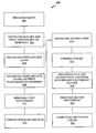
- FIG. 11 therein is shown a simplified process chart 600 of the present invention which includes: providing wafer 602 ; depositing bitlines and first photoresist on periphery 604 ; depositing wordline-gate layer and first photoresist on periphery 606 ; implanting wordline-gate layer and first photoresist 608 ; removing first photoresist 610 ; forming wordline and gate 612 ; depositing spacer layer 614 ; forming spacer 616 ; implanting gate and source/drain junctions with second photoresist on core 618 ; removing second photoresist 620 ; completing integrated circuit 622 .
Abstract
Description
- 1. Technical Field
- The present invention relates generally to semiconductor technology and more specifically to reducing the number of steps in forming MirrorBit® Flash memory.
- 2. Background Art
- Different types of memories have been developed in the past as electronic memory media for computers and similar systems. Such memories include electrically erasable programmable read only memory (EEPROM) and electrically programmable read only memory (EPROM). Each type of memory had advantages and disadvantages. EEPROM can be easily erased without extra exterior equipment but with reduced data storage density, lower speed, and higher cost. EPROM, in contrast, is less expensive and has greater density but lacks erasability.
- A newer type of memory called “Flash” EEPROM, or Flash memory, has become extremely popular because it combines the advantages of the high density and low cost of EPROM with the electrical erasability of EEPROM. Flash memory can be rewritten and can hold its contents without power. It is used in many portable electronic products, such as cell phone, portable computers, voice recorders, etc. as well as in many larger electronic systems, such as cars, planes, industrial control systems, etc.
- In Flash memory, bits of information are programmed individually as in the older types of memory, such as dynamic random access memory (DRAM) and static random access memory (SRAM) memory chips. However, in DRAMs and SRAMs where individual bits can be erased one at a time, Flash memory must currently be erased in fixed multi-bit blocks or sectors.
- Conventionally, Flash memory is constructed of many Flash memory cells where a single bit is stored in each memory cell and the cells are programmed by hot electron injection and erased by Fowler-Nordheim tunneling. However, increased market demand has driven the development of Flash memory cells to increase both the speed and the density. Newer Flash memory cells have been developed that allow more than a single bit to be stored in each cell.
- One memory cell structure involves the storage of more than one level of charge to be stored in a memory cell with each level representative of a bit. This structure is referred to as a multi-level storage (MLS) architecture. Unfortunately, this structure inherently requires a great deal of precision in both programming and reading the differences in the levels to be able to distinguish the bits. If a memory cell using the MLS architecture is overcharged, even by a small amount, the only way to correct the bit error would be to erase the memory cell and totally reprogram the memory cell. The need in the MLS architecture to precisely control the amount of charge in a memory cell while programming also makes the technology slower and the data less reliable. It also takes longer to access or “read” precise amounts of charge. Thus, both speed and reliability are sacrificed in order to improve memory cell density.
- An even newer technology allowing multiple bits to be stored in a single cell is known as “MirrorBit®” Flash memory has been developed. In this technology, a memory cell is essentially split into two identical (mirrored) parts, each of which is formulated for storing one of two independent bits. Each MirrorBit Flash memory cell, like a traditional Flash cell, has a gate with a source and a drain. However, unlike a traditional Flash cell in which the source is always connected to an electrical source and the drain is always connected to an electrical drain, each MirrorBit Flash memory cell can have the connections of the source and drain reversed during operation to permit the storing of two bits.
- The MirrorBit Flash memory cell has a semiconductor substrate with dopant implanted conductive bitlines. A multilayer storage layer, referred to as a “charge-trapping dielectric layer”, is formed over the semiconductor substrate. The charge-trapping dielectric layer can generally be composed of three separate layers: a first insulating layer, a charge-trapping layer, and a second insulating layer. Wordlines are formed over the charge-trapping dielectric layer perpendicular to the bitlines. Programming circuitry controls two bits per cell by applying a signal to the wordline, which acts as a control gate, and changing bitline connections such that one bit is stored by source and drain being connected in one arrangement and a complementary bit is stored by the source and drain being interchanged in another arrangement.
- Programming of the cell is accomplished in one direction and reading is accomplished in a direction opposite that in which it is programmed.
- A major problem in the past has been that the core and the periphery were implanted with dopant at the same time and, as devices became smaller, it was found that this implant would cause short-circuiting of the buried bitlines because of the difficulty in controlling implant density with smaller devices.
- A solution to this problem has been long sought but has long eluded those skilled in the art.
- The present invention provides a method of manufacturing an integrated circuit with a semiconductor substrate having a core region and a periphery region. A charge-trapping dielectric layer is deposited in the core region, and a gate dielectric layer is deposited in the periphery region. Bitlines are formed in the semiconductor substrate in the core region and not in the periphery region. A wordline-gate layer is formed and implanted with dopant in the core region and not in the periphery region. A wordline and a gate are then formed. Source/drain junctions and the gate are implanted with dopant in the periphery region and not in the core region. This method eliminates the problem of the short-circuiting of the buried bitlines because of the difficulty in controlling implant density with smaller devices.
- The above and additional advantages of the present invention will become apparent to those skilled in the art from a reading of the following detailed description when taken in conjunction with the accompanying drawings.
- FIG. 1 is a plan view of a MirrorBit Flash EEPROM according to the present invention;
- FIG. 2 is a circuit schematic of a portion of one of the M×N array cores of FIG. 1;
- FIG. 3 is a plan view of a portion of one of the M×N array cores and periphery gates of FIG. 1;
- FIG. 4 is a cross-sectional isometric view of a memory cell along the line 4-4 of FIG. 3;
- FIG. 5 is a cross-sectional view of a partially processed EEPROM in accordance with the present invention;
- FIG. 6 is the structure of FIG. 5 after deposition of a wordline-gate layer and during a dopant implantation process;
- FIG. 7 is the structure of FIG. 6 after formation of the wordlines and the gates;
- FIG. 8 is the structure of FIG. 7 after deposition of a conformal spacer layer;
- FIG. 9 is the structure of FIG. 8 after etching of the conformal stop layer;
- FIG. 10 is the structure of FIG. 9 during a heavy dopant implantation process; and
- FIG. 11 is a simplified flow chart in accordance with the present invention.
- Referring now to FIG. 1, therein is shown a plan view of a MirrorBit® Flash EEPROM 100, which commonly includes a
semiconductor substrate 102 in which one or more high-density core regions and one or more low-density peripheral portions are formed. The EEPROM 100 is manufactured according to the process of the present invention. High-density core regions typically include one or more M×N array cores 104 of individually addressable, substantially identical MirrorBit Flash memory cells. Low-density peripheral portions typically include input/output (I/O) circuitry and programming circuitry for selectively addressing the individual memory cells. The programming circuitry is represented in part by and includes one ormore x-decoders 108 and y-decoders 110, cooperating with I/O circuitry 106 for connecting the source, gate, and drain of selected addressed memory cells to predetermined voltages or impedances to effect designated operations on the memory cell, e.g., programming, reading, and erasing, and deriving necessary voltages to effect such operations. - The term “horizontal” as used in herein is defined as a plane parallel to the conventional plane or surface the
semiconductor substrate 102 regardless of its orientation. The term “vertical” refers to a direction perpendicular to the horizontal as just defined. Terms, such as “on”, “above”, “below”, “higher”, “lower”, “over”, “under”, “thick”, “side” and “beside”, are defined with respect to these horizontal and vertical planes. The terms such as “processed” and “formed” as used herein is defined to include one or more of the following: depositing or growing semiconductor materials, masking, patterning, photolithography, etching, implanting, removal, and/or stripping. - Referring now to FIG. 2, therein is shown a circuit schematic of a portion of one of the M×
N array cores 104 of FIG. 1. The circuit schematic shows a line ofmemory cells 200, which includesmemory cells 201 through 204 and which together can form an 8-bit word. Each of thememory cells 201 through 204 is connected to awordline 206, which acts as a control gate. Each of thememory cells 201 through 204 has two associated bitlines with most of the memory cells having a common bitline. Thememory cell 201 has associatedbitlines memory cell 202 has associatedbitlines memory cell 203 has associatedbitlines memory cell 204 has associatedbitlines - Depending upon a signal on the wordline and the connection of the bitlines in a memory cell to an electrical source or drain, the
memory cells 201 through 204 are capable of writing, reading, and erasing bits atlocations 215 through 222. For example, control of the bit atlocation 215 is achieved through connection of the drain to thebitline 208 and the source to thebitline 209. Similarly, control of the bit atlocation 216 is achieved through connection of the drain to thebitline 209 and the source to thebitline 208. Although adjacent memory cells share common bitlines, the adjacent memory cells do not interfere with each other because the memory cells are programmed one at a time and only one memory cell is active at a time while programming. - Referring now to FIG. 3, therein is shown a plan view of a portion of one of the M×
N array cores 104 of FIG. 1. Thesemiconductor substrate 102 has a plurality of dopant implantedbitlines 304 extending in parallel with a plurality of formedwordlines 302 extending in parallel and at right angles to the plurality of dopant implantedbitlines 304. Thewordlines 302 andbitlines 304 have contacts and interconnections (not shown) totransistors 306 of the programming circuitry represented in part byx-decoders 108 and y-decoders 110 of FIG. 1. - Referring now to FIG. 4, therein is shown a cross-sectional isometric view of a typical MirrorBit Flash memory cell along the line 4-4 of FIG. 3, such as a
memory cell 400. Thesemiconductor substrate 102 is a p-doped silicon substrate with athreshold adjustment implant 402 of a p-type material, such as boron. Thethreshold adjustment implant 402 provides a region that is more heavily doped than thesemiconductor substrate 102 itself and assists in the control of the threshold voltage of thememory cell 400. - A charge-trapping
dielectric layer 404 is deposited over thesemiconductor substrate 102. The charge-trappingdielectric layer 404 generally can be composed of three separate layers: a first insulatinglayer 406, a charge-trapping layer 408, and a second insulatinglayer 410. The first and second insulatinglayers trapping layer 408 is of a nitride dielectric such as silicon nitride (SixNy). The oxide-nitride-oxide configuration is frequently referred to as a matter of convenience as an “ONO layer”. - The
bitlines 304 of FIG. 3 are implanted with dopant under the charge-trappingdielectric layer 404 in thesemiconductor substrate 102 as typified by first and secondconductive bitlines conductive bitlines threshold adjustment implant 402, which is achannel 416. - A material, such as polysilicon, is deposited over the charge-trapping
dielectric layer 404, patterned, etched, and stripped resulting in awordline 418. Thewordline 418 is one of thewordlines 302 in FIG. 3. - It is understood that the implementation of each step in manufacturing has associated processing steps.
- The
locations 420 through 422 indicate where bits can be stored in thememory cell 400 andlocations memory cell 400. - Referring now to FIG. 5, therein is shown a cross-sectional view of a partially processed
EEPROM 500, which has asilicon substrate 506, acore region 502, which will be densely covered with MirrorBit Flash cells when processing is complete, and aperiphery region 504, which will be less dense and will have other control devices thereon. - In the
core region 502, where memory cells are to be formed, a p-type silicon substrate 506 has been implanted or processed with a p-typethreshold adjustment implant 508. A charge-trappingdielectric layer 510 is deposited over thesilicon substrate 506. The charge-trappingdielectric layer 510 generally can be composed of three separate layers: a first insulatinglayer 512, a charge-trapping layer 514, and a second insulatinglayer 516. The first and second insulatinglayers trapping layer 514 may be of a nitride dielectric such as silicon nitride (SiN) to form an ONO layer. It will be noted that the present invention is not limited to specific dielectric or charge-trapping materials. Thebitlines 518 through 520, which may be n-type bitlines, are implanted with dopant under the charge-trappingdielectric layer 510 in thesilicon substrate 506. - In the
periphery region 504, wheretransistors 306 will be formed, the p-type silicon substrate 506 has been implanted or processed with the p-typethreshold adjustment implant 508. Agate dielectric layer 522 is deposited on thesilicon substrate 506. Thegate dielectric layer 522 generally is a gate oxide, or silicon dioxide. Deposited over thegate dielectric layer 522 is abitline photoresist layer 523, which assures that bitlines are not implanted into theperiphery region 504. - Referring now to FIG. 6, therein is shown the structure of FIG. 5 after deposition of a
wordline-gate layer 524 and during a dopant implantation process 525. Prior to the dopant implantation process 525, aperiphery photoresist layer 526 is deposited and patterned so as to cover theperiphery region 504. - The
wordline-gate layer 524 is generally amorphous polysilicon and theperiphery photoresist layer 526 is generally of an organic photoresist material. Where the transistors and memory cell are of a NPN-type structure, the dopant implantation process 525 will generally be of an n-type dopant. However, the present invention may be used with PNP-type structures in which case the dopant implantation process 525 will use a p-type dopant. The dopant implantation process 525 forms a dopedregion 527 in the top of thewordline-gate layer 524. - Referring now to FIG. 7, therein is shown the structure of FIG. 6 after formation of
wordlines 528 andgates 530. Theperiphery photoresist layer 526 is removed and thewordline-gate layer 524 is processed to form thewordlines 528 and thegates 530. Although not shown in FIG. 7, thewordlines 528 generally have rectangular cross-sections and will have dopedregions 527 on the top. It will be noted that at this point, thegates 530 will not be implanted with dopant because theperiphery photoresist layer 526 would have covered them during the dopant implantation process 525. - Referring now to FIG. 8, therein is shown the structure of FIG. 7 after deposition of a
conformal spacer layer 532. Theconformal spacer layer 532 may be of materials such as silicon oxide, silicon nitride, or silicon oxynitride. Optionally, lightly doped source/drain junctions or extensions are also formed. - Referring now to FIG. 9, therein is shown the structure of FIG. 8 after etching of a
conformal stop layer 532 to formspacers 534 around thegates 530 and thewordlines 524. - Referring now to FIG. 10, therein is shown the structure of FIG. 9 during a heavy
dopant implantation process 538. Acore photoresist layer 536 has been deposited over the core to protect the bitline isolation areas, which are designated by the p in FIG. 3, from a heavydopant implantation process 538, which implants the source/drain junctions 540 and thegate doping implants 542 in theperiphery region 504. Again, the dopant for the heavydopant implantation process 538 will be dependant upon the NPN or PNP structure of the devices. - With the removal of the
core photoresist layer 536, this portion of theEEPROM 100 is ready to be further processed into a completed integrated circuit. - Referring now to FIG. 11, therein is shown a
simplified process chart 600 of the present invention which includes: providingwafer 602; depositing bitlines and first photoresist on periphery 604; depositing wordline-gate layer and first photoresist onperiphery 606; implanting wordline-gate layer andfirst photoresist 608; removingfirst photoresist 610; forming wordline andgate 612; depositingspacer layer 614; formingspacer 616; implanting gate and source/drain junctions with second photoresist oncore 618; removing second photoresist 620; completingintegrated circuit 622. - Various alternative sequences, additions, and deletions to this process chart would be obvious to those skilled in the art from a detailed reading of the present disclosure. Various implementations of the method may be used in different electronic devices and especially the dual bit memory cell architecture may be achieved according to one or more aspects of the present invention. In particular, the invention is applicable to memory devices wherein both bits in a dual bit cell are used for data or information storage.
- While the invention has been described in conjunction with a specific best mode, it is to be understood that many alternatives, modifications, and variations will be apparent to those skilled in the art in light of the aforegoing description. Accordingly, it is intended to embrace all such alternatives, modifications, and variations that fall within the spirit and scope of the included claims. All matters hither-to-fore set forth or shown in the accompanying drawings are to be interpreted in an illustrative and non-limiting sense.
Claims (20)
Priority Applications (9)
| Application Number | Priority Date | Filing Date | Title |
|---|---|---|---|
| US10/118,732 US8673716B2 (en) | 2002-04-08 | 2002-04-08 | Memory manufacturing process with bitline isolation |
| KR10-2004-7016142A KR20050003357A (en) | 2002-04-08 | 2003-02-14 | Memory manufacturing process with bitline isolation |
| EP03746534A EP1493185B1 (en) | 2002-04-08 | 2003-02-14 | Memory manufacturing process with bitline isolation |
| PCT/US2003/004461 WO2003088353A1 (en) | 2002-04-08 | 2003-02-14 | Memory manufacturing process with bitline isolation |
| JP2003585178A JP2005522880A (en) | 2002-04-08 | 2003-02-14 | Method for manufacturing a memory having bit line insulation |
| DE60329993T DE60329993D1 (en) | 2002-04-08 | 2003-02-14 | MEMORY MANUFACTURING PROCESS WITH BIT LEAD INSULATION |
| AU2003225570A AU2003225570A1 (en) | 2002-04-08 | 2003-02-14 | Memory manufacturing process with bitline isolation |
| CNB038077450A CN1315180C (en) | 2002-04-08 | 2003-02-14 | Memory manufacturing process with bitline isolation |
| TW092106883A TWI271822B (en) | 2002-04-08 | 2003-03-27 | Memory manufacturing process with bitline isolation |
Applications Claiming Priority (1)
| Application Number | Priority Date | Filing Date | Title |
|---|---|---|---|
| US10/118,732 US8673716B2 (en) | 2002-04-08 | 2002-04-08 | Memory manufacturing process with bitline isolation |
Publications (2)
| Publication Number | Publication Date |
|---|---|
| US20030190786A1 true US20030190786A1 (en) | 2003-10-09 |
| US8673716B2 US8673716B2 (en) | 2014-03-18 |
Family
ID=28674480
Family Applications (1)
| Application Number | Title | Priority Date | Filing Date |
|---|---|---|---|
| US10/118,732 Active 2025-09-26 US8673716B2 (en) | 2002-04-08 | 2002-04-08 | Memory manufacturing process with bitline isolation |
Country Status (9)
| Country | Link |
|---|---|
| US (1) | US8673716B2 (en) |
| EP (1) | EP1493185B1 (en) |
| JP (1) | JP2005522880A (en) |
| KR (1) | KR20050003357A (en) |
| CN (1) | CN1315180C (en) |
| AU (1) | AU2003225570A1 (en) |
| DE (1) | DE60329993D1 (en) |
| TW (1) | TWI271822B (en) |
| WO (1) | WO2003088353A1 (en) |
Cited By (15)
| Publication number | Priority date | Publication date | Assignee | Title |
|---|---|---|---|---|
| US6720133B1 (en) * | 2002-04-19 | 2004-04-13 | Advanced Micro Devices, Inc. | Memory manufacturing process using disposable ARC for wordline formation |
| US7668017B2 (en) | 2005-08-17 | 2010-02-23 | Saifun Semiconductors Ltd. | Method of erasing non-volatile memory cells |
| US7675782B2 (en) | 2002-10-29 | 2010-03-09 | Saifun Semiconductors Ltd. | Method, system and circuit for programming a non-volatile memory array |
| US7692961B2 (en) | 2006-02-21 | 2010-04-06 | Saifun Semiconductors Ltd. | Method, circuit and device for disturb-control of programming nonvolatile memory cells by hot-hole injection (HHI) and by channel hot-electron (CHE) injection |
| US7701779B2 (en) | 2006-04-27 | 2010-04-20 | Sajfun Semiconductors Ltd. | Method for programming a reference cell |
| US7738304B2 (en) | 2002-07-10 | 2010-06-15 | Saifun Semiconductors Ltd. | Multiple use memory chip |
| US7743230B2 (en) | 2003-01-31 | 2010-06-22 | Saifun Semiconductors Ltd. | Memory array programming circuit and a method for using the circuit |
| US7760554B2 (en) | 2006-02-21 | 2010-07-20 | Saifun Semiconductors Ltd. | NROM non-volatile memory and mode of operation |
| US7786512B2 (en) | 2005-07-18 | 2010-08-31 | Saifun Semiconductors Ltd. | Dense non-volatile memory array and method of fabrication |
| US7808818B2 (en) | 2006-01-12 | 2010-10-05 | Saifun Semiconductors Ltd. | Secondary injection for NROM |
| US7964459B2 (en) | 2004-10-14 | 2011-06-21 | Spansion Israel Ltd. | Non-volatile memory structure and method of fabrication |
| US8053812B2 (en) | 2005-03-17 | 2011-11-08 | Spansion Israel Ltd | Contact in planar NROM technology |
| US8253452B2 (en) | 2006-02-21 | 2012-08-28 | Spansion Israel Ltd | Circuit and method for powering up an integrated circuit and an integrated circuit utilizing same |
| US9111985B1 (en) * | 2007-01-11 | 2015-08-18 | Cypress Semiconductor Corporation | Shallow bipolar junction transistor |
| CN105304489A (en) * | 2014-07-01 | 2016-02-03 | 中芯国际集成电路制造(上海)有限公司 | Forming method of semiconductor device |
Families Citing this family (4)
| Publication number | Priority date | Publication date | Assignee | Title |
|---|---|---|---|---|
| US8673716B2 (en) | 2002-04-08 | 2014-03-18 | Spansion Llc | Memory manufacturing process with bitline isolation |
| CN101375390B (en) * | 2006-01-25 | 2013-06-05 | 日本电气株式会社 | Semiconductor device and method for fabricating same |
| JP2012023247A (en) * | 2010-07-15 | 2012-02-02 | Panasonic Corp | Semiconductor storage device and manufacturing method of the same |
| TW201209595A (en) * | 2010-08-26 | 2012-03-01 | Walton Advanced Eng Inc | Storage device with data sharing function |
Citations (7)
| Publication number | Priority date | Publication date | Assignee | Title |
|---|---|---|---|---|
| US4342149A (en) * | 1979-11-23 | 1982-08-03 | Siemens Aktiengesellschaft | Method of making very short channel length MNOS and MOS devices by double implantation of one conductivity type subsequent to other type implantation |
| US4516313A (en) * | 1983-05-27 | 1985-05-14 | Ncr Corporation | Unified CMOS/SNOS semiconductor fabrication process |
| US5815433A (en) * | 1994-12-27 | 1998-09-29 | Nkk Corporation | Mask ROM device with gate insulation film based in pad oxide film and/or nitride film |
| US6436759B1 (en) * | 2001-01-19 | 2002-08-20 | Microelectronics Corp. | Method for fabricating a MOS transistor of an embedded memory |
| US6468838B2 (en) * | 2001-03-01 | 2002-10-22 | United Microelectronic Corp. | Method for fabricating a MOS transistor of an embedded memory |
| US6566194B1 (en) * | 2001-10-01 | 2003-05-20 | Advanced Micro Devices, Inc. | Salicided gate for virtual ground arrays |
| US6797565B1 (en) * | 2002-09-16 | 2004-09-28 | Advanced Micro Devices, Inc. | Methods for fabricating and planarizing dual poly scalable SONOS flash memory |
Family Cites Families (3)
| Publication number | Priority date | Publication date | Assignee | Title |
|---|---|---|---|---|
| US4640844A (en) | 1984-03-22 | 1987-02-03 | Siemens Aktiengesellschaft | Method for the manufacture of gate electrodes formed of double layers of metal silicides having a high melting point and doped polycrystalline silicon |
| EP1039533A3 (en) * | 1999-03-22 | 2001-04-04 | Infineon Technologies North America Corp. | High performance dram and method of manufacture |
| US8673716B2 (en) | 2002-04-08 | 2014-03-18 | Spansion Llc | Memory manufacturing process with bitline isolation |
-
2002
- 2002-04-08 US US10/118,732 patent/US8673716B2/en active Active
-
2003
- 2003-02-14 WO PCT/US2003/004461 patent/WO2003088353A1/en active Application Filing
- 2003-02-14 EP EP03746534A patent/EP1493185B1/en not_active Expired - Fee Related
- 2003-02-14 KR KR10-2004-7016142A patent/KR20050003357A/en not_active Application Discontinuation
- 2003-02-14 DE DE60329993T patent/DE60329993D1/en not_active Expired - Lifetime
- 2003-02-14 JP JP2003585178A patent/JP2005522880A/en active Pending
- 2003-02-14 CN CNB038077450A patent/CN1315180C/en not_active Expired - Lifetime
- 2003-02-14 AU AU2003225570A patent/AU2003225570A1/en not_active Abandoned
- 2003-03-27 TW TW092106883A patent/TWI271822B/en not_active IP Right Cessation
Patent Citations (7)
| Publication number | Priority date | Publication date | Assignee | Title |
|---|---|---|---|---|
| US4342149A (en) * | 1979-11-23 | 1982-08-03 | Siemens Aktiengesellschaft | Method of making very short channel length MNOS and MOS devices by double implantation of one conductivity type subsequent to other type implantation |
| US4516313A (en) * | 1983-05-27 | 1985-05-14 | Ncr Corporation | Unified CMOS/SNOS semiconductor fabrication process |
| US5815433A (en) * | 1994-12-27 | 1998-09-29 | Nkk Corporation | Mask ROM device with gate insulation film based in pad oxide film and/or nitride film |
| US6436759B1 (en) * | 2001-01-19 | 2002-08-20 | Microelectronics Corp. | Method for fabricating a MOS transistor of an embedded memory |
| US6468838B2 (en) * | 2001-03-01 | 2002-10-22 | United Microelectronic Corp. | Method for fabricating a MOS transistor of an embedded memory |
| US6566194B1 (en) * | 2001-10-01 | 2003-05-20 | Advanced Micro Devices, Inc. | Salicided gate for virtual ground arrays |
| US6797565B1 (en) * | 2002-09-16 | 2004-09-28 | Advanced Micro Devices, Inc. | Methods for fabricating and planarizing dual poly scalable SONOS flash memory |
Cited By (15)
| Publication number | Priority date | Publication date | Assignee | Title |
|---|---|---|---|---|
| US6720133B1 (en) * | 2002-04-19 | 2004-04-13 | Advanced Micro Devices, Inc. | Memory manufacturing process using disposable ARC for wordline formation |
| US7738304B2 (en) | 2002-07-10 | 2010-06-15 | Saifun Semiconductors Ltd. | Multiple use memory chip |
| US7675782B2 (en) | 2002-10-29 | 2010-03-09 | Saifun Semiconductors Ltd. | Method, system and circuit for programming a non-volatile memory array |
| US7743230B2 (en) | 2003-01-31 | 2010-06-22 | Saifun Semiconductors Ltd. | Memory array programming circuit and a method for using the circuit |
| US7964459B2 (en) | 2004-10-14 | 2011-06-21 | Spansion Israel Ltd. | Non-volatile memory structure and method of fabrication |
| US8053812B2 (en) | 2005-03-17 | 2011-11-08 | Spansion Israel Ltd | Contact in planar NROM technology |
| US7786512B2 (en) | 2005-07-18 | 2010-08-31 | Saifun Semiconductors Ltd. | Dense non-volatile memory array and method of fabrication |
| US7668017B2 (en) | 2005-08-17 | 2010-02-23 | Saifun Semiconductors Ltd. | Method of erasing non-volatile memory cells |
| US7808818B2 (en) | 2006-01-12 | 2010-10-05 | Saifun Semiconductors Ltd. | Secondary injection for NROM |
| US7760554B2 (en) | 2006-02-21 | 2010-07-20 | Saifun Semiconductors Ltd. | NROM non-volatile memory and mode of operation |
| US7692961B2 (en) | 2006-02-21 | 2010-04-06 | Saifun Semiconductors Ltd. | Method, circuit and device for disturb-control of programming nonvolatile memory cells by hot-hole injection (HHI) and by channel hot-electron (CHE) injection |
| US8253452B2 (en) | 2006-02-21 | 2012-08-28 | Spansion Israel Ltd | Circuit and method for powering up an integrated circuit and an integrated circuit utilizing same |
| US7701779B2 (en) | 2006-04-27 | 2010-04-20 | Sajfun Semiconductors Ltd. | Method for programming a reference cell |
| US9111985B1 (en) * | 2007-01-11 | 2015-08-18 | Cypress Semiconductor Corporation | Shallow bipolar junction transistor |
| CN105304489A (en) * | 2014-07-01 | 2016-02-03 | 中芯国际集成电路制造(上海)有限公司 | Forming method of semiconductor device |
Also Published As
| Publication number | Publication date |
|---|---|
| EP1493185A1 (en) | 2005-01-05 |
| EP1493185B1 (en) | 2009-11-11 |
| WO2003088353A1 (en) | 2003-10-23 |
| CN1647265A (en) | 2005-07-27 |
| AU2003225570A8 (en) | 2003-10-27 |
| JP2005522880A (en) | 2005-07-28 |
| KR20050003357A (en) | 2005-01-10 |
| US8673716B2 (en) | 2014-03-18 |
| CN1315180C (en) | 2007-05-09 |
| DE60329993D1 (en) | 2009-12-24 |
| TWI271822B (en) | 2007-01-21 |
| TW200400601A (en) | 2004-01-01 |
| AU2003225570A1 (en) | 2003-10-27 |
Similar Documents
| Publication | Publication Date | Title |
|---|---|---|
| US6670241B1 (en) | Semiconductor memory with deuterated materials | |
| US8673716B2 (en) | Memory manufacturing process with bitline isolation | |
| US6706595B2 (en) | Hard mask process for memory device without bitline shorts | |
| US6617215B1 (en) | Memory wordline hard mask | |
| US6479348B1 (en) | Method of making memory wordline hard mask extension | |
| KR101136140B1 (en) | Bitline implant utilizing dual poly | |
| US6653190B1 (en) | Flash memory with controlled wordline width | |
| US6653191B1 (en) | Memory manufacturing process using bitline rapid thermal anneal | |
| US8508047B2 (en) | Buried word line memory integrated circuit system | |
| US6803265B1 (en) | Liner for semiconductor memories and manufacturing method therefor | |
| US6620717B1 (en) | Memory with disposable ARC for wordline formation | |
| US6720133B1 (en) | Memory manufacturing process using disposable ARC for wordline formation | |
| US7888218B2 (en) | Using thick spacer for bitline implant then remove | |
| US7053446B1 (en) | Memory wordline spacer | |
| US7176113B1 (en) | LDC implant for mirrorbit to improve Vt roll-off and form sharper junction | |
| US6723605B1 (en) | Method for manufacturing memory with high conductivity bitline and shallow trench isolation integration | |
| US20070166938A1 (en) | Semiconductor device with high conductivity region using shallow trench | |
| US7692236B1 (en) | Multiple dual bit memory integrated circuit system | |
| US6770523B1 (en) | Method for semiconductor wafer planarization by CMP stop layer formation | |
| US7074677B1 (en) | Memory with improved charge-trapping dielectric layer | |
| US7297592B1 (en) | Semiconductor memory with data retention liner | |
| US7052969B1 (en) | Method for semiconductor wafer planarization by isolation material growth | |
| KR100751580B1 (en) | Shield plates for limiting cross coupling between floating gates |
Legal Events
| Date | Code | Title | Description |
|---|---|---|---|
| AS | Assignment |
Owner name: FUJITSU LIMITED, JAPAN Free format text: ASSIGNMENT OF ASSIGNORS INTEREST;ASSIGNORS:RAMSBEY, MARK T.;KAMAL, TAZRIEN;YANG, JEAN Y.;AND OTHERS;SIGNING DATES FROM 20020306 TO 20020322;REEL/FRAME:012781/0554 Owner name: ADVANCED MICRO DEVICES, INC., CALIFORNIA Free format text: ASSIGNMENT OF ASSIGNORS INTEREST;ASSIGNORS:RAMSBEY, MARK T.;KAMAL, TAZRIEN;YANG, JEAN Y.;AND OTHERS;SIGNING DATES FROM 20020306 TO 20020322;REEL/FRAME:012781/0554 Owner name: FUJITSU LIMITED, JAPAN Free format text: ASSIGNMENT OF ASSIGNORS INTEREST;ASSIGNORS:RAMSBEY, MARK T.;KAMAL, TAZRIEN;YANG, JEAN Y.;AND OTHERS;REEL/FRAME:012781/0554;SIGNING DATES FROM 20020306 TO 20020322 Owner name: ADVANCED MICRO DEVICES, INC., CALIFORNIA Free format text: ASSIGNMENT OF ASSIGNORS INTEREST;ASSIGNORS:RAMSBEY, MARK T.;KAMAL, TAZRIEN;YANG, JEAN Y.;AND OTHERS;REEL/FRAME:012781/0554;SIGNING DATES FROM 20020306 TO 20020322 |
|
| AS | Assignment |
Owner name: AMD (U.S.) HOLDINGS, INC., CALIFORNIA Free format text: ASSIGNMENT OF ASSIGNORS INTEREST;ASSIGNOR:ADVANCED MICRO DEVICES, INC.;REEL/FRAME:014763/0107 Effective date: 20040330 |
|
| AS | Assignment |
Owner name: AMD INVESTMENTS, INC., CALIFORNIA Free format text: ASSIGNMENT OF ASSIGNORS INTEREST;ASSIGNOR:AMD (U.S.) HOLDINGS, INC.;REEL/FRAME:014763/0583 Effective date: 20040330 |
|
| AS | Assignment |
Owner name: FASL LLC, CALIFORNIA Free format text: ASSIGNMENT OF ASSIGNORS INTEREST;ASSIGNORS:AMD INVESTMENTS, INC.;FUJITSU LIMITED;SIGNING DATES FROM 20040330 TO 20040514;REEL/FRAME:014770/0236 Owner name: FASL LLC, CALIFORNIA Free format text: ASSIGNMENT OF ASSIGNORS INTEREST;ASSIGNORS:AMD INVESTMENTS, INC.;FUJITSU LIMITED;REEL/FRAME:014770/0236;SIGNING DATES FROM 20040330 TO 20040514 |
|
| AS | Assignment |
Owner name: SPANSION LLC, CALIFORNIA Free format text: CHANGE OF NAME;ASSIGNOR:FASL LLC;REEL/FRAME:030818/0050 Effective date: 20040628 |
|
| STCF | Information on status: patent grant |
Free format text: PATENTED CASE |
|
| AS | Assignment |
Owner name: MORGAN STANLEY SENIOR FUNDING, INC., NEW YORK Free format text: SECURITY INTEREST;ASSIGNORS:CYPRESS SEMICONDUCTOR CORPORATION;SPANSION LLC;REEL/FRAME:035240/0429 Effective date: 20150312 |
|
| MAFP | Maintenance fee payment |
Free format text: PAYMENT OF MAINTENANCE FEE, 4TH YEAR, LARGE ENTITY (ORIGINAL EVENT CODE: M1551) Year of fee payment: 4 |
|
| AS | Assignment |
Owner name: MUFG UNION BANK, N.A., CALIFORNIA Free format text: ASSIGNMENT AND ASSUMPTION OF SECURITY INTEREST IN INTELLECTUAL PROPERTY;ASSIGNOR:MORGAN STANLEY SENIOR FUNDING, INC.;REEL/FRAME:050896/0366 Effective date: 20190731 |
|
| AS | Assignment |
Owner name: MORGAN STANLEY SENIOR FUNDING, INC., NEW YORK Free format text: CORRECTIVE ASSIGNMENT TO CORRECT THE 8647899 PREVIOUSLY RECORDED ON REEL 035240 FRAME 0429. ASSIGNOR(S) HEREBY CONFIRMS THE SECURITY INTERST;ASSIGNORS:CYPRESS SEMICONDUCTOR CORPORATION;SPANSION LLC;REEL/FRAME:058002/0470 Effective date: 20150312 |
|
| MAFP | Maintenance fee payment |
Free format text: PAYMENT OF MAINTENANCE FEE, 8TH YEAR, LARGE ENTITY (ORIGINAL EVENT CODE: M1552); ENTITY STATUS OF PATENT OWNER: LARGE ENTITY Year of fee payment: 8 |
|
| AS | Assignment |
Owner name: SPANSION LLC, CALIFORNIA Free format text: RELEASE BY SECURED PARTY;ASSIGNOR:MUFG UNION BANK, N.A.;REEL/FRAME:059410/0438 Effective date: 20200416 Owner name: CYPRESS SEMICONDUCTOR CORPORATION, CALIFORNIA Free format text: RELEASE BY SECURED PARTY;ASSIGNOR:MUFG UNION BANK, N.A.;REEL/FRAME:059410/0438 Effective date: 20200416 |
|
| AS | Assignment |
Owner name: INFINEON TECHNOLOGIES LLC, CALIFORNIA Free format text: ASSIGNMENT OF ASSIGNORS INTEREST;ASSIGNOR:CYPRESS SEMICONDUCTOR CORPORATION;REEL/FRAME:059721/0467 Effective date: 20200315 |