US20030190811A1 - Elimination of resist footing on tera hardmask - Google Patents
Elimination of resist footing on tera hardmask Download PDFInfo
- Publication number
- US20030190811A1 US20030190811A1 US10/114,484 US11448402A US2003190811A1 US 20030190811 A1 US20030190811 A1 US 20030190811A1 US 11448402 A US11448402 A US 11448402A US 2003190811 A1 US2003190811 A1 US 2003190811A1
- Authority
- US
- United States
- Prior art keywords
- layer
- hardmask
- resist
- sio
- photoresist
- Prior art date
- Legal status (The legal status is an assumption and is not a legal conclusion. Google has not performed a legal analysis and makes no representation as to the accuracy of the status listed.)
- Granted
Links
Images


Classifications
-
- H—ELECTRICITY
- H01—ELECTRIC ELEMENTS
- H01L—SEMICONDUCTOR DEVICES NOT COVERED BY CLASS H10
- H01L21/00—Processes or apparatus adapted for the manufacture or treatment of semiconductor or solid state devices or of parts thereof
- H01L21/02—Manufacture or treatment of semiconductor devices or of parts thereof
- H01L21/027—Making masks on semiconductor bodies for further photolithographic processing not provided for in group H01L21/18 or H01L21/34
- H01L21/033—Making masks on semiconductor bodies for further photolithographic processing not provided for in group H01L21/18 or H01L21/34 comprising inorganic layers
- H01L21/0332—Making masks on semiconductor bodies for further photolithographic processing not provided for in group H01L21/18 or H01L21/34 comprising inorganic layers characterised by their composition, e.g. multilayer masks, materials
-
- G—PHYSICS
- G03—PHOTOGRAPHY; CINEMATOGRAPHY; ANALOGOUS TECHNIQUES USING WAVES OTHER THAN OPTICAL WAVES; ELECTROGRAPHY; HOLOGRAPHY
- G03F—PHOTOMECHANICAL PRODUCTION OF TEXTURED OR PATTERNED SURFACES, e.g. FOR PRINTING, FOR PROCESSING OF SEMICONDUCTOR DEVICES; MATERIALS THEREFOR; ORIGINALS THEREFOR; APPARATUS SPECIALLY ADAPTED THEREFOR
- G03F7/00—Photomechanical, e.g. photolithographic, production of textured or patterned surfaces, e.g. printing surfaces; Materials therefor, e.g. comprising photoresists; Apparatus specially adapted therefor
- G03F7/004—Photosensitive materials
- G03F7/09—Photosensitive materials characterised by structural details, e.g. supports, auxiliary layers
- G03F7/091—Photosensitive materials characterised by structural details, e.g. supports, auxiliary layers characterised by antireflection means or light filtering or absorbing means, e.g. anti-halation, contrast enhancement
Definitions
- the invention relates to a method of manufacturing a wafer stack comprising a deep trench (DT) level, wherein the deposited TERA hardmask has a substrate reflectivity below 0.8 percent, but wherein the resist printed on to wafer is free from creating an interaction between the resist-hardmask, and is therefore free from the disadvantage of “footing”.
- DT deep trench
- Photoresists are photo sensitive films that are used for transfer of an image to a substrate, and entails coating the photoresists on a substrate and exposing it through a photomask to a source of activating radiation.
- the photomask is comprised of areas that are opaque to activating radiation and other areas that are transparent to activating radiation.
- the exposure to activating radiation creates a photoinduced chemical transformation of the photoresist coating to transfer a pattern from the photomask to the photoresist coated substrate. After exposure the photoresist is developed to form a relief image that allows selective processing of the substrate.
- the photoresist may be either positive-acting or negative-acting.
- the negative-acting photoresists coating the layer portions that are exposed to activating radiation crosslinks or polymerizes a reaction between a photoactive compound and polymerizable reagents of the photoresist, so that exposed coating portions are made less soluble in a developer solution than unexposed portions.
- Proper photoresist processing is one of the keys to obtaining a small ground rule, efficient wafer stack for a DT level on the semiconductor.
- U.S. Pat. No. 6,261,743 B1 disclose a method of forming a photoresist relief image that substantially reduces “notching” and “footing” comprising:
- An object of the present invention is to provide a process to manufacture a wafer stack, wherein the hardmask deposited on the substrate has a reflectivity below about 0.8%, so that a single layer resist (SLR) printed on the wafer shows no standing waves, and prevents interaction between the resist-hardmask, to thereby alleviate “footing” or the failure to clear during development that results in an upwardly tapering release image sidewall.
- SLR single layer resist
- the invention is accomplished by forming a layer of hardmask material on a photoresist disposed on a substrate; subjecting the hardmask to an oxidation step to form a cap; depositing a layer of SiO 2 on top of the cap layer; and patterning and developing the layer of photoresist to obtain a substrate reflectivity below 0.8%, without the occurrence of “standing waves”, and without “footing”.
- FIG. 1 depicts a prior art wafer stack comprising a DT level, and shows an oxide layer disposed on the hardmask to form a cap layer.
- FIG. 2 shows a scanning electron microscope (SEM) picture of a prior art wafer stack comprising a DT level with a 193-nm resist layer on the substrate (the resist is sensitive to 193 nm laser, and its thickness is about 350-nm).
- SEM scanning electron microscope
- FIG. 3 depicts a wafer stack comprising a DT level formed by the method of the invention, which inserts a blocking layer of SiO 2 between the cap layer and the resist.
- FIG. 4 shows substrate reflectivity as a function of the stack and is a graph of substrate reflectivity versus cap layer thickness for a prior art wafer stack comprising a DT level.
- FIG. 5 shows substrate reflectivity as a function of the stack and is a graph of the substrate reflectivity versus the thickness of the inserted blocking layer of SiO 2 , formed by the process of the present invention.
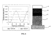
- FIG. 6 shows substrate reflectivity as a function of the stack and is a graph showing substrate reflectivity versus SiO 2 thickness for a stack formed by the process of the invention in which the cap thickness is 25 nm+/ ⁇ 5 nm.
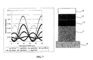
- FIG. 7 shows a graph of substrate reflectivity versus SiO 2 thickness and a corollary wafer stack comprising a DT level for cap thicknesses varying from about 20 nm to about 32 nm, resulting from the process of the invention.
- FIG. 8 is a cross-sectional view of a SEM picture of a wafer stack with DT level and SiO 2 cap, where the standing waves are caused by high substrate reflectivity, due to the fact that stack thickness is not optimized.
- FIG. 1 depicts a prior art wafer stack comprising a deep trench level.
- a substrate of borosilicate glass (BSG) 10 on which there is deposited a hardmask 11 .
- the hardmask is oxidized to form a cap layer 12 , upon which a resist layer 13 is deposited.
- the tunable etch resistance ARC (anti reflective coating) hardmask is deposited at a thickness of about 200 nm, whereupon in a subsequent deposition step, an oxygen flow is introduced to provide about a 25 nm+/ ⁇ 5 nm cap layer.
- This hardmask has a substrate reflectivity below 0.8%, and resist printed on this wafer exhibits no standing waves, however, a resist-hardmask interaction is nevertheless formed, which leads to “footing” or the failure to clear during development that results in an upwardly tapering release image sidewall.
- the hardmask in FIG. 1 is a bottom anti-reflective coating (BARC) having a thickness of about 200 nm.
- BARC bottom anti-reflective coating
- the hardmask optical constants for FIG. 1 are defined as the index of refraction n and the extinction coefficient k.
- the ARC—hardmask and resist may be modeled so as to find the optimum optical parameters (n and k values) of the ARC hardmask layer as well as the optimum thickness.
- a knowledge of the optical constants of the entire film structure is needed in order to compute the minimal reflectance at ARC-hardmask and resist interface.
- Computations are based on algorithms which use the Fresnel coefficients, as found in standard text books such as OPTICS, by Hecht and A. Zajak, 1979, Wiley, pgs. 312-313.
- the wafer stack comprising a DT level formed by the method of the invention is depicted in FIG. 3, and shows the insertion of a blocking layer of SiO 2 14 between the resist 13 and the cap layer 12 , which is a tunable etch resistance ARC (TERA).
- the TERA layer is a vapor deposited SiO 2 , and may function as a antireflective coating, hardmask or a combined antireflective coating/hardmask for high resolution lithography. By inserting the SiO 2 layer between the resist and TERA/cap layer, the interaction between TERA/cap layer and resist is blocked, and therefore prevents footing.
- Substrate reflectivity as a function of the wafer stack of the prior art is shown in the graph of FIG. 4, which depicts substrate reflectivity versus cap layer thickness. As shown from this graph, if the cap layer thickness is controlled within 25+/ ⁇ 10 nm, preferably between 20 nm-35 nm, substrate reflectivity is ⁇ 0.8%.
- FIG. 3 Substrate reflectivity as a function of the wafer stack prepared by the process of the invention (FIG. 3) is shown in FIG. 5, which depicts substrate reflectivity versus the thickness of SiO2.
- FIG. 6 pertains to substrate reflectivity as a function of the wafer stack of the invention process, where substrate reflectivity versus thickness of SiO 2 is depicted.
- a SiO 2 layer may be utilized at a thickness ranging from slightly more than 0 to about 100 nm, preferably about 20 nm due to etching considerations.
- a graph of substrate reflectivity versus SiO 2 thickness is shown in FIG. 7 along with a corollary wafer stack comprising a DT level for cap thickness ranging from about 20 nm to about 32 nm, prepared by the process of the invention.
- a cap thickness of 25 nm+/ ⁇ 5 nm is chosen, an SiO 2 thickness can be chosen ranging from about slightly more than 0 to about 100 nm, preferably about 20 nm due to etch considerations.
- FIG. 8 A cross-sectional view of a SEM picture of a wafer stack with DT level and a SiO 2 layer is shown in FIG. 8; however, the structure is characterized by standing waves, due to high substrate reflectivity in excess of 0.8 percent.
Abstract
Description
- 1. Field of the Invention
- The invention relates to a method of manufacturing a wafer stack comprising a deep trench (DT) level, wherein the deposited TERA hardmask has a substrate reflectivity below 0.8 percent, but wherein the resist printed on to wafer is free from creating an interaction between the resist-hardmask, and is therefore free from the disadvantage of “footing”.
- 2. Description of the Related Art
- Increased demand for high performance in semiconductor devices has necessitated smaller ground rules, in part, to permit increased processing speed. Consistent with the demand for high performance semiconductor devices, is the corollary of finer and finer patterning of resist images to attain higher integration. To satisfy this requirement, development and improvement of lithographic techniques using short-wave length exposure tools such as deep-ultraviolet (DUV) has been employed.
- Photoresists (resists) are photo sensitive films that are used for transfer of an image to a substrate, and entails coating the photoresists on a substrate and exposing it through a photomask to a source of activating radiation. The photomask is comprised of areas that are opaque to activating radiation and other areas that are transparent to activating radiation. The exposure to activating radiation creates a photoinduced chemical transformation of the photoresist coating to transfer a pattern from the photomask to the photoresist coated substrate. After exposure the photoresist is developed to form a relief image that allows selective processing of the substrate.
- The photoresist may be either positive-acting or negative-acting. In the negative-acting photoresists coating the layer portions that are exposed to activating radiation crosslinks or polymerizes a reaction between a photoactive compound and polymerizable reagents of the photoresist, so that exposed coating portions are made less soluble in a developer solution than unexposed portions.
- For a positive-acting photoresist, exposed portions are made more soluble in a developer solution while areas not exposed are less soluble in the developer solution.
- Proper photoresist processing is one of the keys to obtaining a small ground rule, efficient wafer stack for a DT level on the semiconductor.
- Unfortunately, at the critical levels required for high performance semiconductor devices where density lines are required to be increased for a wafer stack for a DT level, a single layer resist approach cannot fulfill both the lithography and etch requirements, due to the fact that, even though use of a TERA hardmask produces a substrate reflectivity below 0.8 percent without any standing waves, nevertheless, a resist-hardmask interaction occurs that results in “footing”.
- Lee et al., Inorganic ARC for 0.18 μm and Sub-0.18 μm Multilevel Interconnects 1998 IEEE 98, 84-86 disclose a novel designed inorganic ARC for deep-UV lithography and implementation of the ARC into multi-level metal interconnects for sub-micron technologies using SixOyNz ARC to reduce substrate reflectivity to a minimum and prevent DUV resist footing, while allowing the novel ARC to serve as a hardmask for metal etch.
- In-situ hardmask and metal etch in a single etcher to develop a semiconductor device with a layer of photoresist patterned and developed free from resist footing is disclosed in U.S. Pat. No. 6,159,863. The process entails:
- forming active devices in and on a substrate in the semiconductor wafer;
- forming an interlayer dielectric on a surface of the semiconductor wafer;
- forming a metal layer on the surface of the interlayer dielectric;
- forming a layer of hardmask material on the surface of the metal layer;
- forming a layer of photoresist on the layer of hardmask material;
- patterning and developing the layer of photoresist exposing portions of the hardmask material underlying the layer of photoresist;
- placing the semiconductor wafer in an etcher;
- etching the exposed portions of the layer of hardmask material exposing portions of the metal layer
- underlying the layer of hardmask material; and
- without removing the semiconductor wafer from the etcher etching the exposed portions of the metal layer.
- U.S. Pat. No. 6,261,743 B1 disclose a method of forming a photoresist relief image that substantially reduces “notching” and “footing” comprising:
- (a) applying on a substrate a layer of an antireflective composition comprising a photoacid generator
- compound, an acid or thermal acid generator compound and a crosslinker, and crosslinking the antireflective layer;
- (b) applying a layer of the photoresist composition over the antireflective composition layer;
- (c) exposing the photoresist layer to activating radiation whereby the photoacid generator of the antireflective composition generates acid; and
- (d) developing the exposed photoresist.
- In manufacturing a wafer stack comprising a deep trench (DT) level, in which a hardmask is deposited on a substrate to provide the necessary reflectivity below 0.8%, there is a need to enable a single layer resist (SLR) printed on the wafer, in which there are no standing waves, to also prevent interaction between the resist-hardmask that leads to footing and the drawbacks attendant thereto.
- An object of the present invention is to provide a process to manufacture a wafer stack, wherein the hardmask deposited on the substrate has a reflectivity below about 0.8%, so that a single layer resist (SLR) printed on the wafer shows no standing waves, and prevents interaction between the resist-hardmask, to thereby alleviate “footing” or the failure to clear during development that results in an upwardly tapering release image sidewall.
- In general, the invention is accomplished by forming a layer of hardmask material on a photoresist disposed on a substrate; subjecting the hardmask to an oxidation step to form a cap; depositing a layer of SiO 2 on top of the cap layer; and patterning and developing the layer of photoresist to obtain a substrate reflectivity below 0.8%, without the occurrence of “standing waves”, and without “footing”.
- FIG. 1 depicts a prior art wafer stack comprising a DT level, and shows an oxide layer disposed on the hardmask to form a cap layer.
- FIG. 2 shows a scanning electron microscope (SEM) picture of a prior art wafer stack comprising a DT level with a 193-nm resist layer on the substrate (the resist is sensitive to 193 nm laser, and its thickness is about 350-nm).
- FIG. 3 depicts a wafer stack comprising a DT level formed by the method of the invention, which inserts a blocking layer of SiO 2 between the cap layer and the resist.
- FIG. 4 shows substrate reflectivity as a function of the stack and is a graph of substrate reflectivity versus cap layer thickness for a prior art wafer stack comprising a DT level.
- FIG. 5 shows substrate reflectivity as a function of the stack and is a graph of the substrate reflectivity versus the thickness of the inserted blocking layer of SiO 2, formed by the process of the present invention.
- FIG. 6 shows substrate reflectivity as a function of the stack and is a graph showing substrate reflectivity versus SiO 2 thickness for a stack formed by the process of the invention in which the cap thickness is 25 nm+/−5 nm.
- FIG. 7 shows a graph of substrate reflectivity versus SiO 2 thickness and a corollary wafer stack comprising a DT level for cap thicknesses varying from about 20 nm to about 32 nm, resulting from the process of the invention.
- FIG. 8 is a cross-sectional view of a SEM picture of a wafer stack with DT level and SiO 2 cap, where the standing waves are caused by high substrate reflectivity, due to the fact that stack thickness is not optimized.
- In describing the method for eliminating resist footing on a hardmask in the context of the invention, reference is now made to FIG. 1 which depicts a prior art wafer stack comprising a deep trench level. In this figure, there is shown a substrate of borosilicate glass (BSG) 10 on which there is deposited a
hardmask 11. The hardmask is oxidized to form acap layer 12, upon which aresist layer 13 is deposited. In this figure, the tunable etch resistance ARC (anti reflective coating) hardmask is deposited at a thickness of about 200 nm, whereupon in a subsequent deposition step, an oxygen flow is introduced to provide about a 25 nm+/−5 nm cap layer. This hardmask has a substrate reflectivity below 0.8%, and resist printed on this wafer exhibits no standing waves, however, a resist-hardmask interaction is nevertheless formed, which leads to “footing” or the failure to clear during development that results in an upwardly tapering release image sidewall. - The footing resulting from the prior art wafer stack structure of the prior art of the FIG. 1 lithographic profile is shown in the scanning electron microscope (SEM) picture of FIG. 2, where the 193-nm resist layer is of a thickness of approximately 350 nm on the structure.
- The hardmask in FIG. 1 is a bottom anti-reflective coating (BARC) having a thickness of about 200 nm.
- The hardmask optical constants for FIG. 1 are defined as the index of refraction n and the extinction coefficient k. Generally speaking, the ARC—hardmask and resist may be modeled so as to find the optimum optical parameters (n and k values) of the ARC hardmask layer as well as the optimum thickness. To obtain this end, a knowledge of the optical constants of the entire film structure is needed in order to compute the minimal reflectance at ARC-hardmask and resist interface. Computations are based on algorithms which use the Fresnel coefficients, as found in standard text books such as OPTICS, by Hecht and A. Zajak, 1979, Wiley, pgs. 312-313. The n value for the hardmask in FIG. 1 is n=2.1 and the k value for the hardmask in FIG. 1 is k=0.65 for 200 nm.
- The wafer stack comprising a DT level formed by the method of the invention is depicted in FIG. 3, and shows the insertion of a blocking layer of
SiO 2 14 between the resist 13 and thecap layer 12, which is a tunable etch resistance ARC (TERA). The TERA layer is a vapor deposited SiO2, and may function as a antireflective coating, hardmask or a combined antireflective coating/hardmask for high resolution lithography. By inserting the SiO2 layer between the resist and TERA/cap layer, the interaction between TERA/cap layer and resist is blocked, and therefore prevents footing. The thickness of the TERA layer is 200 nm, while n=2.1 and k=0.65. The thickness of the cap layer is 25+/−10 nm, while n=1.8 and k=0.2. For the SiO2 layer, n=1.56 and k=0. - Substrate reflectivity as a function of the wafer stack of the prior art is shown in the graph of FIG. 4, which depicts substrate reflectivity versus cap layer thickness. As shown from this graph, if the cap layer thickness is controlled within 25+/−10 nm, preferably between 20 nm-35 nm, substrate reflectivity is ≦0.8%.
- Substrate reflectivity as a function of the wafer stack prepared by the process of the invention (FIG. 3) is shown in FIG. 5, which depicts substrate reflectivity versus the thickness of SiO2.
- FIG. 6 pertains to substrate reflectivity as a function of the wafer stack of the invention process, where substrate reflectivity versus thickness of SiO 2 is depicted. When a cap thickness of 25 nm+/−5 nm is chosen, a SiO2 layer may be utilized at a thickness ranging from slightly more than 0 to about 100 nm, preferably about 20 nm due to etching considerations.
- A graph of substrate reflectivity versus SiO 2 thickness is shown in FIG. 7 along with a corollary wafer stack comprising a DT level for cap thickness ranging from about 20 nm to about 32 nm, prepared by the process of the invention. Again, if a cap thickness of 25 nm+/−5 nm is chosen, an SiO2 thickness can be chosen ranging from about slightly more than 0 to about 100 nm, preferably about 20 nm due to etch considerations.
- A cross-sectional view of a SEM picture of a wafer stack with DT level and a SiO 2 layer is shown in FIG. 8; however, the structure is characterized by standing waves, due to high substrate reflectivity in excess of 0.8 percent.
- Although the invention has been described by way of specific embodiments, it is to be understood that the invention is not intended to be limited to this description, but instead only to the extent set forth in the following claims.
Claims (22)
Priority Applications (2)
| Application Number | Priority Date | Filing Date | Title |
|---|---|---|---|
| US10/114,484 US6815367B2 (en) | 2002-04-03 | 2002-04-03 | Elimination of resist footing on tera hardmask |
| DE10313893A DE10313893A1 (en) | 2002-04-03 | 2003-03-27 | Avoiding the formation of a resist base on a TERA hard mask |
Applications Claiming Priority (1)
| Application Number | Priority Date | Filing Date | Title |
|---|---|---|---|
| US10/114,484 US6815367B2 (en) | 2002-04-03 | 2002-04-03 | Elimination of resist footing on tera hardmask |
Publications (2)
| Publication Number | Publication Date |
|---|---|
| US20030190811A1 true US20030190811A1 (en) | 2003-10-09 |
| US6815367B2 US6815367B2 (en) | 2004-11-09 |
Family
ID=28673696
Family Applications (1)
| Application Number | Title | Priority Date | Filing Date |
|---|---|---|---|
| US10/114,484 Expired - Lifetime US6815367B2 (en) | 2002-04-03 | 2002-04-03 | Elimination of resist footing on tera hardmask |
Country Status (2)
| Country | Link |
|---|---|
| US (1) | US6815367B2 (en) |
| DE (1) | DE10313893A1 (en) |
Cited By (2)
| Publication number | Priority date | Publication date | Assignee | Title |
|---|---|---|---|---|
| US20050100682A1 (en) * | 2003-11-06 | 2005-05-12 | Tokyo Electron Limited | Method for depositing materials on a substrate |
| CN102354087A (en) * | 2011-11-03 | 2012-02-15 | 中国科学院半导体研究所 | Method for improving photoresist exposure precision |
Families Citing this family (1)
| Publication number | Priority date | Publication date | Assignee | Title |
|---|---|---|---|---|
| US7497959B2 (en) * | 2004-05-11 | 2009-03-03 | International Business Machines Corporation | Methods and structures for protecting one area while processing another area on a chip |
Citations (10)
| Publication number | Priority date | Publication date | Assignee | Title |
|---|---|---|---|---|
| US538244A (en) * | 1895-04-30 | Harmonic scale for pianos | ||
| US602294A (en) * | 1898-04-12 | Island | ||
| US5098095A (en) * | 1991-05-06 | 1992-03-24 | Weiss Twice Toys, Inc. | Pump ball |
| US5830605A (en) * | 1995-08-29 | 1998-11-03 | Ricoh Optical Industries Co., Ltd. | Gradation mask method of producing the same and method of forming special surface profile on material using gradation mask |
| US5886102A (en) * | 1996-06-11 | 1999-03-23 | Shipley Company, L.L.C. | Antireflective coating compositions |
| US6300240B1 (en) * | 1999-07-23 | 2001-10-09 | Worldwide Semiconductor Manufacturing Corp. | Method for forming bottom anti-reflective coating (BARC) |
| US6303275B1 (en) * | 2000-02-10 | 2001-10-16 | International Business Machines Corporation | Method for resist filling and planarization of high aspect ratio features |
| US6329117B1 (en) * | 1997-10-08 | 2001-12-11 | Clariant International, Ltd. | Antireflection or light-absorbing coating composition and polymer therefor |
| US6518200B2 (en) * | 2001-06-07 | 2003-02-11 | Taiwan Semiconductor Manufacturing Co., Ltd. | Graded composite layer and method for fabrication thereof |
| US6573189B1 (en) * | 2001-11-07 | 2003-06-03 | Taiwan Semiconductor Manufacturing Company | Manufacture method of metal bottom ARC |
Family Cites Families (2)
| Publication number | Priority date | Publication date | Assignee | Title |
|---|---|---|---|---|
| US5939236A (en) | 1997-02-07 | 1999-08-17 | Shipley Company, L.L.C. | Antireflective coating compositions comprising photoacid generators |
| US6159863A (en) | 1999-01-22 | 2000-12-12 | Advanced Micro Devices, Inc. | Insitu hardmask and metal etch in a single etcher |
-
2002
- 2002-04-03 US US10/114,484 patent/US6815367B2/en not_active Expired - Lifetime
-
2003
- 2003-03-27 DE DE10313893A patent/DE10313893A1/en not_active Withdrawn
Patent Citations (10)
| Publication number | Priority date | Publication date | Assignee | Title |
|---|---|---|---|---|
| US538244A (en) * | 1895-04-30 | Harmonic scale for pianos | ||
| US602294A (en) * | 1898-04-12 | Island | ||
| US5098095A (en) * | 1991-05-06 | 1992-03-24 | Weiss Twice Toys, Inc. | Pump ball |
| US5830605A (en) * | 1995-08-29 | 1998-11-03 | Ricoh Optical Industries Co., Ltd. | Gradation mask method of producing the same and method of forming special surface profile on material using gradation mask |
| US5886102A (en) * | 1996-06-11 | 1999-03-23 | Shipley Company, L.L.C. | Antireflective coating compositions |
| US6329117B1 (en) * | 1997-10-08 | 2001-12-11 | Clariant International, Ltd. | Antireflection or light-absorbing coating composition and polymer therefor |
| US6300240B1 (en) * | 1999-07-23 | 2001-10-09 | Worldwide Semiconductor Manufacturing Corp. | Method for forming bottom anti-reflective coating (BARC) |
| US6303275B1 (en) * | 2000-02-10 | 2001-10-16 | International Business Machines Corporation | Method for resist filling and planarization of high aspect ratio features |
| US6518200B2 (en) * | 2001-06-07 | 2003-02-11 | Taiwan Semiconductor Manufacturing Co., Ltd. | Graded composite layer and method for fabrication thereof |
| US6573189B1 (en) * | 2001-11-07 | 2003-06-03 | Taiwan Semiconductor Manufacturing Company | Manufacture method of metal bottom ARC |
Cited By (4)
| Publication number | Priority date | Publication date | Assignee | Title |
|---|---|---|---|---|
| US20050100682A1 (en) * | 2003-11-06 | 2005-05-12 | Tokyo Electron Limited | Method for depositing materials on a substrate |
| WO2005048329A1 (en) | 2003-11-06 | 2005-05-26 | Tokyo Electron Limited | Method for depositing materials on a substrate |
| JP2007511073A (en) * | 2003-11-06 | 2007-04-26 | 東京エレクトロン株式会社 | A method of depositing material on a substrate. |
| CN102354087A (en) * | 2011-11-03 | 2012-02-15 | 中国科学院半导体研究所 | Method for improving photoresist exposure precision |
Also Published As
| Publication number | Publication date |
|---|---|
| US6815367B2 (en) | 2004-11-09 |
| DE10313893A1 (en) | 2003-11-13 |
Similar Documents
| Publication | Publication Date | Title |
|---|---|---|
| US6030541A (en) | Process for defining a pattern using an anti-reflective coating and structure therefor | |
| US8258056B2 (en) | Method and material for forming a double exposure lithography pattern | |
| US7109119B2 (en) | Scum solution for chemically amplified resist patterning in cu/low k dual damascene | |
| US6720256B1 (en) | Method of dual damascene patterning | |
| US7759253B2 (en) | Method and material for forming a double exposure lithography pattern | |
| US8168372B2 (en) | Method of creating photolithographic structures with developer-trimmed hard mask | |
| JP4420592B2 (en) | Method for forming fine pattern of semiconductor element | |
| CN101335198B (en) | Method for forming fine pattern of semiconductor device | |
| US8536031B2 (en) | Method of fabricating dual damascene structures using a multilevel multiple exposure patterning scheme | |
| JP3306678B2 (en) | Method of forming metal pattern film | |
| US20050170655A1 (en) | Reticle fabrication using a removable hard mask | |
| US8268535B2 (en) | Pattern formation method | |
| JP4481902B2 (en) | Pattern formation method by multilayer resist method | |
| US9058997B2 (en) | Process of multiple exposures with spin castable films | |
| JP2764542B2 (en) | Fine resist pattern forming method | |
| EP0586860A2 (en) | Photoresist composition and process for forming a pattern using the same | |
| US6815367B2 (en) | Elimination of resist footing on tera hardmask | |
| JP2636763B2 (en) | Method for manufacturing semiconductor device | |
| WO1999052018A1 (en) | Thin layer imaging process for microlithography using radiation at strongly attenuated wavelengths | |
| US6090523A (en) | Multi-resin material for an antireflection film to be formed on a workpiece disposed on a semiconductor substrate | |
| US5744293A (en) | Semiconductor device having antireflective layer containing organic resin with dispersed carbon particles | |
| KR20070071679A (en) | Composition for hard mask and method for manufacturing semiconductor device | |
| JPH05234965A (en) | Formation of contact hole | |
| TW550695B (en) | Method to remove bottom anti-reflection coating layer | |
| US6183938B1 (en) | Conformal organic coatings for sidewall patterning of sublithographic structures |
Legal Events
| Date | Code | Title | Description |
|---|---|---|---|
| AS | Assignment |
Owner name: INFINEON TECHNOLOGIES NORTH AMERICA CORP., CALIFOR Free format text: ASSIGNMENT OF ASSIGNORS INTEREST;ASSIGNOR:CHEN, XIAOCHUN LINDA;REEL/FRAME:012781/0929 Effective date: 20020401 |
|
| AS | Assignment |
Owner name: INFINEON TECHNOLOGIES AG, GERMANY Free format text: ASSIGNMENT OF ASSIGNORS INTEREST;ASSIGNOR:INFINEON TECHNOLOGIES NORTH AMERICA CORP.;REEL/FRAME:013722/0372 Effective date: 20030603 |
|
| STCF | Information on status: patent grant |
Free format text: PATENTED CASE |
|
| FPAY | Fee payment |
Year of fee payment: 4 |
|
| AS | Assignment |
Owner name: QIMONDA AG, GERMANY Free format text: ASSIGNMENT OF ASSIGNORS INTEREST;ASSIGNOR:INFINEON TECHNOLOGIES AG;REEL/FRAME:023773/0457 Effective date: 20060425 |
|
| FPAY | Fee payment |
Year of fee payment: 8 |
|
| AS | Assignment |
Owner name: INFINEON TECHNOLOGIES AG, GERMANY Free format text: ASSIGNMENT OF ASSIGNORS INTEREST;ASSIGNOR:QIMONDA AG;REEL/FRAME:035623/0001 Effective date: 20141009 |
|
| AS | Assignment |
Owner name: POLARIS INNOVATIONS LIMITED, IRELAND Free format text: ASSIGNMENT OF ASSIGNORS INTEREST;ASSIGNOR:INFINEON TECHNOLOGIES AG;REEL/FRAME:036818/0583 Effective date: 20150708 |
|
| FPAY | Fee payment |
Year of fee payment: 12 |
|
| SULP | Surcharge for late payment |
Year of fee payment: 11 |