US20030191259A1 - Novel polymers for photoresist and photoresist compositions using the same - Google Patents
Novel polymers for photoresist and photoresist compositions using the same Download PDFInfo
- Publication number
- US20030191259A1 US20030191259A1 US10/394,606 US39460603A US2003191259A1 US 20030191259 A1 US20030191259 A1 US 20030191259A1 US 39460603 A US39460603 A US 39460603A US 2003191259 A1 US2003191259 A1 US 2003191259A1
- Authority
- US
- United States
- Prior art keywords
- substituted
- norbornene
- photoresist
- ene
- bicyclo
- Prior art date
- Legal status (The legal status is an assumption and is not a legal conclusion. Google has not performed a legal analysis and makes no representation as to the accuracy of the status listed.)
- Granted
Links
- 0 C[C@](*1)C(C2C(O3)=N)C=CC1C2C3=N Chemical compound C[C@](*1)C(C2C(O3)=N)C=CC1C2C3=N 0.000 description 10
- KNDQHSIWLOJIGP-UHFFFAOYSA-N O=C1OC(=O)C2C3C=CC(C3)C12 Chemical compound O=C1OC(=O)C2C3C=CC(C3)C12 KNDQHSIWLOJIGP-UHFFFAOYSA-N 0.000 description 7
- RMAZRAQKPTXZNL-UHFFFAOYSA-N COC(=O)C1CC2C=CC1C2 Chemical compound COC(=O)C1CC2C=CC1C2 RMAZRAQKPTXZNL-UHFFFAOYSA-N 0.000 description 6
- ATGAIMAJZGYQKM-UHFFFAOYSA-N COC(=O)C1C2CC(C1C(=O)O)C(C1C(=O)OC(=O)C1C1C3CC(CC3C(=O)OC(C)(C)C)C1C1C(C)C3CC1C1C(=O)OC(=O)C31)C2C1C2CC(C(=O)O)C(C2)C1C Chemical compound COC(=O)C1C2CC(C1C(=O)O)C(C1C(=O)OC(=O)C1C1C3CC(CC3C(=O)OC(C)(C)C)C1C1C(C)C3CC1C1C(=O)OC(=O)C31)C2C1C2CC(C(=O)O)C(C2)C1C ATGAIMAJZGYQKM-UHFFFAOYSA-N 0.000 description 2
- ROMOIEJUMLHTOD-UHFFFAOYSA-N *.CC(CC(CC1C(=O)OC(=O)C1C1C2CCC(CC2)C1C)C(=O)OC(C)(C)C)C(=O)O Chemical compound *.CC(CC(CC1C(=O)OC(=O)C1C1C2CCC(CC2)C1C)C(=O)OC(C)(C)C)C(=O)O ROMOIEJUMLHTOD-UHFFFAOYSA-N 0.000 description 1
- DUXHVCSJEPLGFO-UHFFFAOYSA-N CC1C(CC2C3CC(CC3O)C2CC2C(=O)OC(=O)C2C2C(CC3C(C)C4CC3C3C(=O)OC(=O)C43)C3CC(C(=O)OC(C)(C)C)C2C3)C2CC(C(=O)O)C1C2 Chemical compound CC1C(CC2C3CC(CC3O)C2CC2C(=O)OC(=O)C2C2C(CC3C(C)C4CC3C3C(=O)OC(=O)C43)C3CC(C(=O)OC(C)(C)C)C2C3)C2CC(C(=O)O)C1C2 DUXHVCSJEPLGFO-UHFFFAOYSA-N 0.000 description 1
- KVFJEIDFLISHQY-UHFFFAOYSA-N CC1C2CC(CC2C(=O)O)C1C1C(C2C(=O)OC(=O)C2C2C3CC(CC3C(=O)OC(C)(C)C)C2C2C(C)C3CC2C2C(=O)OC(=O)C32)C2CC1C(CO)(CO)C2 Chemical compound CC1C2CC(CC2C(=O)O)C1C1C(C2C(=O)OC(=O)C2C2C3CC(CC3C(=O)OC(C)(C)C)C2C2C(C)C3CC2C2C(=O)OC(=O)C32)C2CC1C(CO)(CO)C2 KVFJEIDFLISHQY-UHFFFAOYSA-N 0.000 description 1
- DSZXKSDBSSTTDC-UHFFFAOYSA-N CC1C2CCC(CC2C(=O)O)C1C1C(C2C(=O)OC(=O)C2C2C3CC(CC3C(=O)OC(C)(C)C)C2C2C(C)C3CC2C2C(=O)OC(=O)C32)C2CCC1C(CO)(CO)C2 Chemical compound CC1C2CCC(CC2C(=O)O)C1C1C(C2C(=O)OC(=O)C2C2C3CC(CC3C(=O)OC(C)(C)C)C2C2C(C)C3CC2C2C(=O)OC(=O)C32)C2CCC1C(CO)(CO)C2 DSZXKSDBSSTTDC-UHFFFAOYSA-N 0.000 description 1
- YWFZILREZJZETB-UHFFFAOYSA-N CC1C2CCC(CC2C(=O)O)C1C1C2CCC(CC2O)C1C1C(=O)OC(=O)C1C1C2CCC(CC2C(=O)OC(C)(C)C)C1C1C(C)C2CCC1C1C(=O)OC(=O)C21 Chemical compound CC1C2CCC(CC2C(=O)O)C1C1C2CCC(CC2O)C1C1C(=O)OC(=O)C1C1C2CCC(CC2C(=O)OC(C)(C)C)C1C1C(C)C2CCC1C1C(=O)OC(=O)C21 YWFZILREZJZETB-UHFFFAOYSA-N 0.000 description 1
- FPYJFEHAWHCUMM-UHFFFAOYSA-N O=C1C=CC(=O)O1 Chemical compound O=C1C=CC(=O)O1 FPYJFEHAWHCUMM-UHFFFAOYSA-N 0.000 description 1
- CSDFGPJHCDGBLF-UHFFFAOYSA-N [H]C1(CO)CC2CC1C(C1C3CC(C(=O)O)C(C3)C1C)C2C1C(=O)OC(=O)C1C1C2CC(CC2C(=O)OC(C)(C)C)C1C1C(C)C2CC1C1C(=O)OC(=O)C21 Chemical compound [H]C1(CO)CC2CC1C(C1C3CC(C(=O)O)C(C3)C1C)C2C1C(=O)OC(=O)C1C1C2CC(CC2C(=O)OC(C)(C)C)C1C1C(C)C2CC1C1C(=O)OC(=O)C21 CSDFGPJHCDGBLF-UHFFFAOYSA-N 0.000 description 1
- HQKASWYPZRMGGS-UHFFFAOYSA-N [H]C1(CO)CC2CCC1C(C1C3CCC(C(C(=O)O)C3)C1C)C2C1C(=O)OC(=O)C1C1C2CCC(CC2C(=O)OC(C)(C)C)C1C1C(C)C2CCC1C1C(=O)OC(=O)C21 Chemical compound [H]C1(CO)CC2CCC1C(C1C3CCC(C(C(=O)O)C3)C1C)C2C1C(=O)OC(=O)C1C1C2CCC(CC2C(=O)OC(C)(C)C)C1C1C(C)C2CCC1C1C(=O)OC(=O)C21 HQKASWYPZRMGGS-UHFFFAOYSA-N 0.000 description 1
Classifications
-
- C—CHEMISTRY; METALLURGY
- C08—ORGANIC MACROMOLECULAR COMPOUNDS; THEIR PREPARATION OR CHEMICAL WORKING-UP; COMPOSITIONS BASED THEREON
- C08F—MACROMOLECULAR COMPOUNDS OBTAINED BY REACTIONS ONLY INVOLVING CARBON-TO-CARBON UNSATURATED BONDS
- C08F232/00—Copolymers of cyclic compounds containing no unsaturated aliphatic radicals in a side chain, and having one or more carbon-to-carbon double bonds in a carbocyclic ring system
- C08F232/08—Copolymers of cyclic compounds containing no unsaturated aliphatic radicals in a side chain, and having one or more carbon-to-carbon double bonds in a carbocyclic ring system having condensed rings
-
- G—PHYSICS
- G03—PHOTOGRAPHY; CINEMATOGRAPHY; ANALOGOUS TECHNIQUES USING WAVES OTHER THAN OPTICAL WAVES; ELECTROGRAPHY; HOLOGRAPHY
- G03F—PHOTOMECHANICAL PRODUCTION OF TEXTURED OR PATTERNED SURFACES, e.g. FOR PRINTING, FOR PROCESSING OF SEMICONDUCTOR DEVICES; MATERIALS THEREFOR; ORIGINALS THEREFOR; APPARATUS SPECIALLY ADAPTED THEREFOR
- G03F7/00—Photomechanical, e.g. photolithographic, production of textured or patterned surfaces, e.g. printing surfaces; Materials therefor, e.g. comprising photoresists; Apparatus specially adapted therefor
- G03F7/004—Photosensitive materials
- G03F7/039—Macromolecular compounds which are photodegradable, e.g. positive electron resists
- G03F7/0392—Macromolecular compounds which are photodegradable, e.g. positive electron resists the macromolecular compound being present in a chemically amplified positive photoresist composition
- G03F7/0395—Macromolecular compounds which are photodegradable, e.g. positive electron resists the macromolecular compound being present in a chemically amplified positive photoresist composition the macromolecular compound having a backbone with alicyclic moieties
Definitions
- the present invention relates to photoresist monomers, polymers formed therefrom, and photoresist compositions containing same, more specifically, photoresist monomers, polymers and a photoresist compositions suitable for photolithography processes employing DUV (deep ultraviolet) light sources such as KrF (249 nm) and ArF(193 nm); EUV; VUV; E-beam; ion-beam; and X-ray.
- DUV deep ultraviolet
- photoresists have been investigated in order to achieve high sensitivity in minute image formation processes for preparing semiconductor devices.
- Such photoresists are prepared by blending a photoacid generator and matrix resin polymer having acid labile group.
- the photoacid generator According to the reaction mechanism of such a photoresist, the photoacid generator generates acid when it is illuminated by a light source, and the main chain or branched chain of the resin is reacted with the generated acid to be decomposed or crosslinked.
- the polarity change of the resin induces solubility differences between the exposed portion and unexposed portion in the developing solution, to form a predetermined pattern.
- resolution depends upon the wavelength of the light source—the shorter the wavelength, the more minute pattern can be formed.
- a photoresist (hereinafter, abbreviated to as “PR”) must satisfy various requisites such as excellent etching resistance, heat resistance and adhesiveness, and more preferably, it should be developable in 2.38% aqueous tetramethylammonium hydroxide (TMAH) solution.
- TMAH aqueous tetramethylammonium hydroxide
- a polymer having a polyacrylate main chain can be easily synthesized, but it has poor etching resistance and has difficulties in the developing process.
- etching resistance it has been considered to add an alicyclic unit to the main chain.
- Bell Research Center developed a polymer having the following chemical structure, wherein the main chain is substituted with norbornene, acrylate and maleic anhydride units.
- the above polymer has a problem in that the maleic anhydride moiety (‘A’ portion), which is employed to polymerize alicyclic olefin groups, is readily dissolved in 2.38 wt % aqueous TMAH solution even in an unexposed condition.
- ‘A’ portion the maleic anhydride moiety
- the ratio of ‘Y’ portion having tert-butyl substituent should be increased, but this results in a relative decrease of the ‘Z’ portion (which has a role of increasing adhesiveness to the substrate), and therefore the PR might be easily separated from the substrate at the time of patterning.
- An object of the present invention is to provide PR monomers which can form polymers having excellent etching resistance, adhesiveness and photosensitivity, and processes for preparing the same.
- Another object of the present invention is to provide PR polymers having excellent etching resistance, adhesiveness and photosensitivity, wherein the unexposed portion is not easily dissolved by developing solution, and processes for preparing the same.
- Another object of the present invention is to provide photoresist compositions using the novel photoresist polymers described above, and processes for preparing the same.
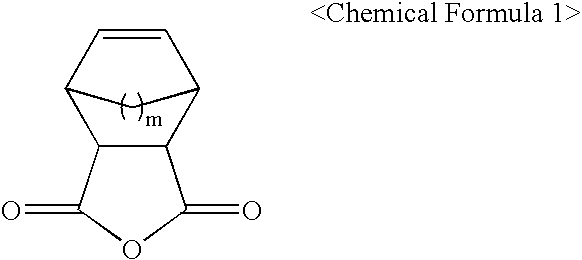
- the present invention provides a photoresist monomer represented by the following Chemical Formula 1.
- m is 1 or 2.
- photoresist copolymer comprising said monomer of Formula 1.
- photoresist copolymers of the present invention comprise (i) a compound represented by the above mentioned Chemical Formula 1 as a first comonomer, and (ii) as a 2 nd comonomer, a compound represented by the following Chemical Formula 2:
- R* is an acid-labile group
- l is 1 or 2.
- a photoresist composition which includes (i) a photoresist copolymer according to the present invention, (ii) a photoacid generator and (iii) an organic solvent.
- m is 1 or 2.
- R* is an acid-labile group
- l is 1 or 2.
- the R* is released when it is reacted with the acid generated by the photoacid generator.
- the photoresist polymer in the exposed region becomes soluble in the developing solution
- the polymer in the unexposed region is not dissolved in the developing solution because acid is not generated therein and thus the acid labile groups are still bound to the photoresist polymer.
- a predetermined pattern is formed.
- the compound of Chemical Formula 2 has a role of enhancing photosensitivity of the photoresist polymer by increasing the difference in solubility in the developing solution between the exposed portion and the unexposed portion of the photo resist.
- the acid labile group R* can have any structure that can be dissociated from the main alicyclic structure by reacting with an acid
- preferable acid labile groups are tert-butyl, 2-tetrahydrofuranyl, 2-tetrahydropyranyl, 2-ethoxyethyl or t-butoxyethyl.
- the photoresist copolymer according to the present invention can be prepared by using a polymerization initiator or by using a metal catalyst.
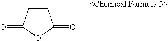
- a polymerization initiator maleic anhydride(Chemical formula 3) or maleimide derivatives can be added as a polymerization-enhancing monomer which makes the polymerization reaction between cycloolefin compounds more efficient.
- maleic anhydride(Chemical formula 3) or maleimide derivatives can be added as a polymerization-enhancing monomer which makes the polymerization reaction between cycloolefin compounds more efficient.
- such polymerization-enhancing monomer is not necessarily required.
- a compound having alcohol groups as represented by the following Chemical Formula 4 can be further added as a monomer in order to intensify adhesion of the photoresist to the substrate.
- a monomer having at least one carboxylic acid group which is represented by the following Chemical Formula 5 may be added to the polymer in order to intensify photosensitivity.
- R 1 is —OH or —R-OH
- R is substituted or non-substituted (C 1 -C 10 ) alkyl, substituted or non-substituted (C 1 -C 10 ) ether, substituted or non-substituted (C 1 -C 10 ) ester or, substituted or non-substituted (C 1 -C 10 ) ketone,
- R 2 is H or R 1 ,
- R 3 is H or —COOR
- n 1 or 2.
- R4 is —COOH or —R-COOH
- k is 1 or 2 and
- R is as same as defined in the Chemical Formula 4.
- the average molecular weight of the photoresist copolymer according to the present invention is between 3,000 to 100,000.
- a synthesizing method using a polymerization initiator is performed by reacting the comonomers, including at least one of maleic anhydride and maleimide derivative monomer, together in an organic solvent in the presence of a polymerization initiator.
- organic solvents are tetrahydrofuran, dimethylforrnamide, dimethyl sulfoxide, dioxane, methyl ethyl ketone, benzene, toluene or xylene may be used.
- Conventional radical polymerization initiators such as 2,2-azobisisobutyronitile (AIBN), acetyl peroxide, lauryl peroxide and tert-butyl peroxide may be used.
- a photoresist composition according to the present invention which is useful for photolithography processes employing deep ultraviolet light sources such as ArF, may be prepared by dissolving the photoresist copolymer according to the present invention in a conventional organic solvent together with a conventional photoacid generator.
- Sulfide or onium type compounds are preferably used as the photoacid generator.
- the photoacid generator may be one or more compounds selected from the group consisting of diphenyl iodide hexafluorophosphate, diphenyl iodide hexafluoroarsenate, diphenyliodide hexafluoroantimonate, diphenyl p-methoxyphenyl triflate, diphenyl p-toluenyl triflate, diphenyl p-isobutylphenyl triflate, diphenyl p-tert-butylphenyl triflate, triphenylsulfonium hexafluorophosphate, triphenylsulfonium hexafluoroarsenate, triphenylsulfonium hexafluoroantimonate, triphenylsulfonium triflate and dibutylnaphthy
- the photoacid generator is used in an amount of 0.05 to 10% by weight of the photoresist copolymer employed. If the amount of the photoacid generator is less than 0.05% by weight, photosensitivity of the photoresist becomes poor. On the other hand, if the amount is more than 10%, the photoacid generator readily absorbs deep ultraviolet to provide a pattern having poor cross-sectional surface.
- organic solvents such as ethyl 3-ethoxypriopionate, methyl 3-methoxypropionate, cyclohexanone, propylene glycol methyl ether acetate, or the like, may be used.
- the amount of solvent used is 200 to 1000% by weight of the photoresist resin, in order to obtain a photoresist coating of desirable thickness. According to the experiments by the present inventors, when the amount of solvent is 600% by weight, a photoresist coating having a thickness of 0.5 ⁇ m is obtained.
- a conventional photoresist pattern-forming method can be used with the photoresist composition prepared according to the present invention, for example as follows:
- the photoresist composition of the present invention is spin-coated on a silicon wafer to form a thin film, which is then soft-baked (i.e. heated in an oven or on a hot plate at 70 to 200° C., preferably at 80 to 150° C. for 1 to 5 minutes), and exposed to light by using an exposing device employing a deep ultraviolet light source, such as ArF light and KrF light, which has a wavelength below 250 nm. Then, the wafer is post-baked (i.e. heated at 70 to 200° C., more preferably, 100 to 200 ° C). Then, the wafer is impregnated in 2.38% aqueous TMAH developing solution for 1.5 minutes, to obtain a photoresist image.
- a deep ultraviolet light source such as ArF light and KrF light
- the exposure energy is preferably 0.1 to 30 mJ/cm 2 and, instead of the deep ultraviolet light source, an E-beam, X-ray, EUV, VUV(Vacuum Ultra Violet) or similar light source may be used.
- a photoresist composition having excellent etching resistance and adhesiveness can be manufactured in large scale with low production cost, and a semiconductor element having excellent reliability can be prepared therefrom.
- Example 1 The procedure of Example 1 is repeated but using mono-methyl-bicyclo[2,2,2]oct-5-ene-2,3-dicarboxylate (0.15 mole) instead of mono-methyl cis-5-norbornene-endo-2,3-dicarboxylate (0.15 mole), to obtain the compound represented by the following Chemical Formula 102.
- Example 3 The procedure of Example 3 is repeated but using 5-norbornene -2-methanol (0.1 mole) instead of 5-norbornene-2,2-dimethanol (0.1 mole), to obtain the compound represented by the following Chemical Formula 104.
- Example 3 The procedure of Example 3 is repeated but using 5-norbornene-2-ol (0.1 mole) instead of 5-norbornene-2,2-dimethanol (0.1 mole), to obtain the compound represented by the following Chemical Formula 105.
- Example 3 The procedure of Example 3 is repeated but using bicyclo[2,2,2]oct-5-ene-2,2-dimethanol (0.1 mole) instead of 5-norbornene-2,2-dimethanol (0.1 mole), cis-bicyclo[2,2,2]oct-5-ene-2,3-dicarboxylic anhydride (0.2 mole) instead of cis-5-norbornene-endo-2,3-dicarboxylic anhydride, bicyclo[2,2,2]oct-5-ene-2-tert-butyl carboxylate (0.65 mole) instead of tert-butyl 5-norbornene-2-carboxylate, and bicyclo[2,2,2]-oct-5-ene-2-carboxylic acid (0.05 mole) instead of 5-norbornene-2-carboxylic acid, to obtain the compound represented by the following Chemical Formula 106.
- the photoresist copolymer represented by the Chemical Formula 101, obtained from the Example 1 (10 g) is dissolved in 40 g of 3-methoxymethyl propionate, and triphenylsulfonium triflate or dibutyl naphthyl sulfonium triflate(0.01-1 g) as a photoacid generator is added thereto. After stirring, the resultant mixture is filtered through a 0.10 ⁇ m filter to provide a PR composition according to the present invention.
- the photoresist composition thus obtained is coated at 0.6 ⁇ m thickness on the substrate to form a photoresist film, and soft-baked in an oven or on a hot plate of 80 to 150° C. for 1 to 5 minutes.
- an exposing step is performed on the photoresist film with 193 nm ArF light source by using an exposing mask.
- the film is post-baked at 100 to 200° C. and impregnated in 2.38% aqueous TMAH solution for 1.5 minutes to obtain an 0.15 ⁇ m line/space (L/S) pattern.
- Example 9 The procedure of Example 9 is repeated but using the photoresist copolymer represented by the Chemical Formula 102, obtained from the Example 2 (10 g), instead of Example 1, and thereby a 0.15 ⁇ m L/S pattern is formed.
- Example 9 The procedure of Example 9 is repeated but using the photoresist copolymer represented by the Chemical Formula 103, obtained from the Example 3 (10 g) instead of Example 1, and thereby a 0.15 ⁇ m L/S pattern is formed.
Abstract

Description
- The present invention relates to photoresist monomers, polymers formed therefrom, and photoresist compositions containing same, more specifically, photoresist monomers, polymers and a photoresist compositions suitable for photolithography processes employing DUV (deep ultraviolet) light sources such as KrF (249 nm) and ArF(193 nm); EUV; VUV; E-beam; ion-beam; and X-ray.
- Recently, chemical amplification type DUV photoresists have been investigated in order to achieve high sensitivity in minute image formation processes for preparing semiconductor devices. Such photoresists are prepared by blending a photoacid generator and matrix resin polymer having acid labile group.
- According to the reaction mechanism of such a photoresist, the photoacid generator generates acid when it is illuminated by a light source, and the main chain or branched chain of the resin is reacted with the generated acid to be decomposed or crosslinked. The polarity change of the resin induces solubility differences between the exposed portion and unexposed portion in the developing solution, to form a predetermined pattern.
- In the lithography process, resolution depends upon the wavelength of the light source—the shorter the wavelength, the more minute pattern can be formed.
- In general, a photoresist (hereinafter, abbreviated to as “PR”) must satisfy various requisites such as excellent etching resistance, heat resistance and adhesiveness, and more preferably, it should be developable in 2.38% aqueous tetramethylammonium hydroxide (TMAH) solution. However, it is very difficult to synthesize a polymer that satisfies all of these requisites. For example, a polymer having a polyacrylate main chain can be easily synthesized, but it has poor etching resistance and has difficulties in the developing process. In order to secure etching resistance, it has been considered to add an alicyclic unit to the main chain. However, in this case, it is very difficult to form a copolymer wherein the main chain is comprised entirely of alicyclic units.
- As an attempt to solve the problems described above, Bell Research Center developed a polymer having the following chemical structure, wherein the main chain is substituted with norbornene, acrylate and maleic anhydride units.

- However, the above polymer has a problem in that the maleic anhydride moiety (‘A’ portion), which is employed to polymerize alicyclic olefin groups, is readily dissolved in 2.38 wt % aqueous TMAH solution even in an unexposed condition. Thus, in order to inhibit the dissolution of the polymer in the unexposed section, the ratio of ‘Y’ portion having tert-butyl substituent should be increased, but this results in a relative decrease of the ‘Z’ portion (which has a role of increasing adhesiveness to the substrate), and therefore the PR might be easily separated from the substrate at the time of patterning.
- In order to solve the problem, cholesterol type dissolution inhibitors have been added to the polymer to form a two-component system. However, since the amount of the dissolution inhibitor is very high [about 30%(w/w) of the resin], reappearance is low and the production cost is high, thereby making the system unsuitable as a PR.
- An object of the present invention is to provide PR monomers which can form polymers having excellent etching resistance, adhesiveness and photosensitivity, and processes for preparing the same.
- Another object of the present invention is to provide PR polymers having excellent etching resistance, adhesiveness and photosensitivity, wherein the unexposed portion is not easily dissolved by developing solution, and processes for preparing the same.
- Another object of the present invention is to provide photoresist compositions using the novel photoresist polymers described above, and processes for preparing the same.
- In order to achieve the aforementioned objects, the present invention provides a photoresist monomer represented by the following Chemical Formula 1.

- wherein, m is 1 or 2.
- In order to achieve the other objects, the present invention provides photoresist copolymer comprising said monomer of Formula 1. Preferably, photoresist copolymers of the present invention comprise (i) a compound represented by the above mentioned Chemical Formula 1 as a first comonomer,, and (ii) as a 2 nd comonomer, a compound represented by the following Chemical Formula 2:

- wherein,
- R* is an acid-labile group, and
- l is 1 or 2.
- In order to achieve further objects of the present invention, a photoresist composition is provided which includes (i) a photoresist copolymer according to the present invention, (ii) a photoacid generator and (iii) an organic solvent.
- It has been found that polymers formed from the monomer represented by Chemical Formula 1 below (i) shows good etching resistance since it is a cycloolefin compound, (ii) has a good adhesiveness to a semiconductor substrate and (iii) has the preferred photosensitivity.

- wherein, m is 1 or 2.
- Considering the characteristics of the compound represented by the above Chemical Formula 1, we have found that a copolymer which comprises (i) the compound represented by Chemical Formula 1 as a first monomer, and (ii), as a second comonomer, the compound represented by the following Chemical Formula 2, which functions as an dissolution inhibitor, is suitable for photolithography employing short-wavelength light sources.

- wherein,
- R* is an acid-labile group, and
- l is 1 or 2.
- In the Chemical formula 2, the R* is released when it is reacted with the acid generated by the photoacid generator. Thus, while the photoresist polymer in the exposed region becomes soluble in the developing solution, the polymer in the unexposed region is not dissolved in the developing solution because acid is not generated therein and thus the acid labile groups are still bound to the photoresist polymer. As the result, a predetermined pattern is formed.
- In this way, the compound of Chemical Formula 2 has a role of enhancing photosensitivity of the photoresist polymer by increasing the difference in solubility in the developing solution between the exposed portion and the unexposed portion of the photo resist.
- Though the acid labile group R* can have any structure that can be dissociated from the main alicyclic structure by reacting with an acid, preferable acid labile groups are tert-butyl, 2-tetrahydrofuranyl, 2-tetrahydropyranyl, 2-ethoxyethyl or t-butoxyethyl.
- The photoresist copolymer according to the present invention can be prepared by using a polymerization initiator or by using a metal catalyst. In the case of synthesis using a polymerization initiator, maleic anhydride(Chemical formula 3) or maleimide derivatives can be added as a polymerization-enhancing monomer which makes the polymerization reaction between cycloolefin compounds more efficient. However, when performing polymerization using a metal catalyst, such polymerization-enhancing monomer is not necessarily required.
- A compound having alcohol groups, as represented by the following Chemical Formula 4, can be further added as a monomer in order to intensify adhesion of the photoresist to the substrate. In addition, a monomer having at least one carboxylic acid group which is represented by the following Chemical Formula 5 may be added to the polymer in order to intensify photosensitivity.

- wherein,
- R 1 is —OH or —R-OH,
- wherein R is substituted or non-substituted (C 1-C10) alkyl, substituted or non-substituted (C1-C10) ether, substituted or non-substituted (C1-C10) ester or, substituted or non-substituted (C1-C10) ketone,
- R 2 is H or R1,
- R 3 is H or —COOR
- and n is 1 or 2.

- wherein,
- R4 is —COOH or —R-COOH,
- k is 1 or 2 and
- R is as same as defined in the Chemical Formula 4.
- Preferably, the average molecular weight of the photoresist copolymer according to the present invention is between 3,000 to 100,000.
- A synthesizing method using a polymerization initiator is performed by reacting the comonomers, including at least one of maleic anhydride and maleimide derivative monomer, together in an organic solvent in the presence of a polymerization initiator. Presently preferred organic solvents are tetrahydrofuran, dimethylforrnamide, dimethyl sulfoxide, dioxane, methyl ethyl ketone, benzene, toluene or xylene may be used. Conventional radical polymerization initiators such as 2,2-azobisisobutyronitile (AIBN), acetyl peroxide, lauryl peroxide and tert-butyl peroxide may be used.
- Alternatively, conventional synthesizing methods using a metal catalyst can be performed without maleic anhydride and maleimide derivatives.
- A photoresist composition according to the present invention, which is useful for photolithography processes employing deep ultraviolet light sources such as ArF, may be prepared by dissolving the photoresist copolymer according to the present invention in a conventional organic solvent together with a conventional photoacid generator.
- Sulfide or onium type compounds are preferably used as the photoacid generator. The photoacid generator may be one or more compounds selected from the group consisting of diphenyl iodide hexafluorophosphate, diphenyl iodide hexafluoroarsenate, diphenyliodide hexafluoroantimonate, diphenyl p-methoxyphenyl triflate, diphenyl p-toluenyl triflate, diphenyl p-isobutylphenyl triflate, diphenyl p-tert-butylphenyl triflate, triphenylsulfonium hexafluorophosphate, triphenylsulfonium hexafluoroarsenate, triphenylsulfonium hexafluoroantimonate, triphenylsulfonium triflate and dibutylnaphthylsulfonium triflate. The photoacid generator is used in an amount of 0.05 to 10% by weight of the photoresist copolymer employed. If the amount of the photoacid generator is less than 0.05% by weight, photosensitivity of the photoresist becomes poor. On the other hand, if the amount is more than 10%, the photoacid generator readily absorbs deep ultraviolet to provide a pattern having poor cross-sectional surface.
- Conventional organic solvents, such as ethyl 3-ethoxypriopionate, methyl 3-methoxypropionate, cyclohexanone, propylene glycol methyl ether acetate, or the like, may be used. The amount of solvent used is 200 to 1000% by weight of the photoresist resin, in order to obtain a photoresist coating of desirable thickness. According to the experiments by the present inventors, when the amount of solvent is 600% by weight, a photoresist coating having a thickness of 0.5 μm is obtained.
- A conventional photoresist pattern-forming method can be used with the photoresist composition prepared according to the present invention, for example as follows:
- First, the photoresist composition of the present invention is spin-coated on a silicon wafer to form a thin film, which is then soft-baked (i.e. heated in an oven or on a hot plate at 70 to 200° C., preferably at 80 to 150° C. for 1 to 5 minutes), and exposed to light by using an exposing device employing a deep ultraviolet light source, such as ArF light and KrF light, which has a wavelength below 250 nm. Then, the wafer is post-baked (i.e. heated at 70 to 200° C., more preferably, 100 to 200 ° C). Then, the wafer is impregnated in 2.38% aqueous TMAH developing solution for 1.5 minutes, to obtain a photoresist image.
- In the above procedure, the exposure energy is preferably 0.1 to 30 mJ/cm 2 and, instead of the deep ultraviolet light source, an E-beam, X-ray, EUV, VUV(Vacuum Ultra Violet) or similar light source may be used.
- By employing the photoresist composition according to the present invention, a line/space (L/S) photoresist pattern having excellent adhesiveness and resolution is obtained, without patten collapse, even when isolation is not more than 70 nm.
- According to the present invention, a photoresist composition having excellent etching resistance and adhesiveness can be manufactured in large scale with low production cost, and a semiconductor element having excellent reliability can be prepared therefrom.
- The invention is described in more detail by referring to the examples below, but it should be noted that the present invention is by no means restricted to the examples.
- Example 1:
- Synthesis of poly(cis-5-norbornene-endo-2,3-dicarboxylic anhydride/tert-butyl 5-norbornene-2-carboxylate/maleic anhydride/mono-methyl cis-5-norbornene-endo-2,3-dicarboxylate/5-norbornene-2-carboxylic acid)
- Maleic anhydride (1.0 mole), cis-5-norbornene-endo-2,3-dicarboxylic anhydride (0.2 mole), mono-methyl cis-5-norbornene-endo-2,3-dicarboxylate (0.15 mole) and tert-butyl-5-norbornene-2-carboxylate (0.65 mole) are dissolved in tetrahydrofuran. Then, 0.5 to 10 g of AIBN (azobisisobutyronitrile) as a polymerization initiator is added thereto, and the resultant mixture is reacted at about 60-70° C. for 4 to 24 hours under nitrogen or argon atmosphere. The polymer thus obtained is precipitated from ethyl ether or hexane, and dried to obtain the compound represented by the following Chemical Formula 101.

- Example 2:
- Synthesis of poly(cis-5-norbornene-endo-2,3-dicarboxylic anhydride/tert-butyl 5-norbornene-2-carboxylate/maleic anhydride/mono-methyl bicyclo[2,2,2]oct-5-ene-2,3-dicarboxlate/5-norbornene-2-carboxylic acid)
- The procedure of Example 1 is repeated but using mono-methyl-bicyclo[2,2,2]oct-5-ene-2,3-dicarboxylate (0.15 mole) instead of mono-methyl cis-5-norbornene-endo-2,3-dicarboxylate (0.15 mole), to obtain the compound represented by the following Chemical Formula 102.

- Example 3:
- Synthesis of poly(cis-5-norbornene-endo-2,3-dicarboxylic anhydride/tert-butyl 5-norbornene-2-carboxylate/maleic anhydride/5-norbornene-2,2-dimethanol/5-norbornene-2-carboxylic acid)
- Maleic anhydride (1.0 mole), cis-5-norbornene-endo-2,3-dicarboxylic anhydride (0.2 mole), 5-norbornene-2,2-dimethanol (0.1 mole), tert-butyl 5-norbornene-2-carboxylate (0.65 mole) and 5-norbornene-2-carboxylic acid (0.05 mole) are dissolved in tetrahydrofuran..
- Then, 0.5 to 10 g of AIBN (azobisisobutyronitrile) as a polymerization initiator is added thereto, and the resultant mixture is reacted at about 60-70° C for 4 to 24 hours under nitrogen or argon atmosphere. The polymer thus obtained is precipitated from ethyl ether or hexane, and dried to obtain the compound represented by the following Chemical Formula 103.

- Example 4:
- Synthesis of poly(cis-5-norbornene-endo-2,3-dicarboxylic anhydride/tert-butyl 5-norbornene-2-carboxylate/maleic anhydride/5-norbornene-2-methanol/5-norbornene-2-carboxylic acid)
- The procedure of Example 3 is repeated but using 5-norbornene -2-methanol (0.1 mole) instead of 5-norbornene-2,2-dimethanol (0.1 mole), to obtain the compound represented by the following Chemical Formula 104.

- Example 5:
- Synthesis of poly(cis-5-norbornene-endo-2,3-dicarboxylic anhydride/tert-butyl 5-norbornene-2-carboxylate/maleic anhydride/5-norbornene -2-ol/5-norbornene-2-carboxylic acid)
- The procedure of Example 3 is repeated but using 5-norbornene-2-ol (0.1 mole) instead of 5-norbornene-2,2-dimethanol (0.1 mole), to obtain the compound represented by the following Chemical Formula 105.

- Example 6:
- Synthesis of poly(cis-bicyclo[2,2,2]oct-5-ene-2,3-dicarboxylic anhydride/bicyclo[2,2,2]oct-5-ene-2-tert-butyl carboxylate/maleic anhydride/bicyclo[2,2,2]oct-5-ene-2,2-dimethanol/bicyclo[2,2,2]oct-5-ene-2-carboxylic acid)
- The procedure of Example 3 is repeated but using bicyclo[2,2,2]oct-5-ene-2,2-dimethanol (0.1 mole) instead of 5-norbornene-2,2-dimethanol (0.1 mole), cis-bicyclo[2,2,2]oct-5-ene-2,3-dicarboxylic anhydride (0.2 mole) instead of cis-5-norbornene-endo-2,3-dicarboxylic anhydride, bicyclo[2,2,2]oct-5-ene-2-tert-butyl carboxylate (0.65 mole) instead of tert-butyl 5-norbornene-2-carboxylate, and bicyclo[2,2,2]-oct-5-ene-2-carboxylic acid (0.05 mole) instead of 5-norbornene-2-carboxylic acid, to obtain the compound represented by the following Chemical Formula 106.

- Example 7:
- Synthesis of poly(cis-bicyclo[2,2,2]oct-5-ene-2,3-dicarboxylic anhydride/bicyclo[2,2,2]oct-5-ene-2-tert-butyl carboxylate/maleic anhydride/bicyclo[2,2,2]oct-5-ene-2-methanol/bicyclo[2,2,21oct-5-ene-2-carboxylic acid)
- The procedure of Example 6 is repeated but using bicyclo[2,2,2]oct-5-ene-2-methanol (0.1 mole) instead of bicyclo[2,2,2]oct-5-ene-2,2-dimethanol (0.1 mole), to obtain the compound represented by following Chemical Formula 107:

- Example 8:
- Synthesis of poly(cis-bicyclo[2,2,2]oct-5-ene-2,3-dicarboxylic anhydride/bicyclo[2,2,2]oct-5-ene-2-tert-butyl carboxylate/maleic anhydride/bicyclo[2,2,2]oct-5-ene-2-ol/bicyclo[2,2,2]oct-5-ene-2-carboxylic acid)
- The procedure of Example 6 is repeated but using bicyclo[2,2,2]oct-5-ene-2-ol (0.1 mole) instead of bicyclo[2,2,2]oct-5-ene-2-ol (0.1 mole), to obtain the compound represented by following Chemical Formula 108:

- PREPARATION OF PHOTORESIST COMPOSITION AND MICROPATTERN FORMATION
- Example 9
- The photoresist copolymer represented by the Chemical Formula 101, obtained from the Example 1 (10 g) is dissolved in 40 g of 3-methoxymethyl propionate, and triphenylsulfonium triflate or dibutyl naphthyl sulfonium triflate(0.01-1 g) as a photoacid generator is added thereto. After stirring, the resultant mixture is filtered through a 0.10 μm filter to provide a PR composition according to the present invention.
- The photoresist composition thus obtained is coated at 0.6 μm thickness on the substrate to form a photoresist film, and soft-baked in an oven or on a hot plate of 80 to 150° C. for 1 to 5 minutes.
- Then, an exposing step is performed on the photoresist film with 193 nm ArF light source by using an exposing mask. The film is post-baked at 100 to 200° C. and impregnated in 2.38% aqueous TMAH solution for 1.5 minutes to obtain an 0.15 μm line/space (L/S) pattern.
- Example 10
- The procedure of Example 9 is repeated but using the photoresist copolymer represented by the Chemical Formula 102, obtained from the Example 2 (10 g), instead of Example 1, and thereby a 0.15 μm L/S pattern is formed.
- Example 11
- The procedure of Example 9 is repeated but using the photoresist copolymer represented by the Chemical Formula 103, obtained from the Example 3 (10 g) instead of Example 1, and thereby a 0.15 μm L/S pattern is formed.
Claims (24)


Priority Applications (1)
| Application Number | Priority Date | Filing Date | Title |
|---|---|---|---|
| US10/394,606 US6987155B2 (en) | 1998-08-27 | 2003-03-21 | Polymers for photoresist and photoresist compositions using the same |
Applications Claiming Priority (6)
| Application Number | Priority Date | Filing Date | Title |
|---|---|---|---|
| KR35029 | 1998-08-27 | ||
| KR10-1998-0035029A KR100362936B1 (en) | 1998-08-27 | 1998-08-27 | Polymers of Novel Photoresist and Photoresist Compositions Using the Same |
| KR35291 | 1998-08-28 | ||
| KR10-1998-0035291A KR100362935B1 (en) | 1998-08-28 | 1998-08-28 | Novel Photoresist Polymers and Photoresist Compositions Using Them |
| US09/383,475 US6569971B2 (en) | 1998-08-27 | 1999-08-26 | Polymers for photoresist and photoresist compositions using the same |
| US10/394,606 US6987155B2 (en) | 1998-08-27 | 2003-03-21 | Polymers for photoresist and photoresist compositions using the same |
Related Parent Applications (1)
| Application Number | Title | Priority Date | Filing Date |
|---|---|---|---|
| US09/383,475 Division US6569971B2 (en) | 1998-08-27 | 1999-08-26 | Polymers for photoresist and photoresist compositions using the same |
Publications (2)
| Publication Number | Publication Date |
|---|---|
| US20030191259A1 true US20030191259A1 (en) | 2003-10-09 |
| US6987155B2 US6987155B2 (en) | 2006-01-17 |
Family
ID=26634058
Family Applications (2)
| Application Number | Title | Priority Date | Filing Date |
|---|---|---|---|
| US09/383,475 Expired - Fee Related US6569971B2 (en) | 1998-08-27 | 1999-08-26 | Polymers for photoresist and photoresist compositions using the same |
| US10/394,606 Expired - Fee Related US6987155B2 (en) | 1998-08-27 | 2003-03-21 | Polymers for photoresist and photoresist compositions using the same |
Family Applications Before (1)
| Application Number | Title | Priority Date | Filing Date |
|---|---|---|---|
| US09/383,475 Expired - Fee Related US6569971B2 (en) | 1998-08-27 | 1999-08-26 | Polymers for photoresist and photoresist compositions using the same |
Country Status (2)
| Country | Link |
|---|---|
| US (2) | US6569971B2 (en) |
| JP (1) | JP2000080124A (en) |
Families Citing this family (297)
| Publication number | Priority date | Publication date | Assignee | Title |
|---|---|---|---|---|
| JP3952612B2 (en) * | 1998-10-16 | 2007-08-01 | 株式会社セガ | Game device |
| KR100389912B1 (en) * | 1999-12-08 | 2003-07-04 | 삼성전자주식회사 | Alicyclic photosensitive polymer and resist composition comprising the same |
| US20020051932A1 (en) * | 2000-05-31 | 2002-05-02 | Shipley Company, L.L.C. | Photoresists for imaging with high energy radiation |
| KR100527533B1 (en) | 2000-06-21 | 2005-11-09 | 주식회사 하이닉스반도체 | Photoresist Polymer for Top Surface Imaging Process and Photoresist Composition Containing the Same |
| JP4150491B2 (en) * | 2000-07-13 | 2008-09-17 | 富士フイルム株式会社 | Positive photosensitive composition |
| KR20020085041A (en) * | 2001-05-04 | 2002-11-16 | 주식회사 하이닉스반도체 | Maleimide-photoresist polymer containing fluorine and photoresist composition comprising the same |
| KR20020096257A (en) * | 2001-06-19 | 2002-12-31 | 주식회사 하이닉스반도체 | Novel photoresist monomer, polymer thereof and photoresist composition containing it |
| JP2003131381A (en) * | 2001-08-10 | 2003-05-09 | Sumitomo Chem Co Ltd | Positive resist composition |
| US7250475B2 (en) * | 2003-06-26 | 2007-07-31 | Symyx Technologies, Inc. | Synthesis of photoresist polymers |
| WO2005000924A1 (en) * | 2003-06-26 | 2005-01-06 | Symyx Technologies, Inc. | Photoresist polymers |
| EP1641848B1 (en) * | 2003-06-26 | 2007-08-22 | JSR Corporation | Photoresist polymer compositions |
| KR101112545B1 (en) | 2004-12-16 | 2012-03-13 | 스미또모 가가꾸 가부시끼가이샤 | Photosensitive resin and thin film panel comprising pattern made of the photosensitive resin and method for manufacturing the thin film panel |
| JP3881361B1 (en) * | 2005-08-02 | 2007-02-14 | 株式会社コナミデジタルエンタテインメント | Sound output device, sound output method and program |
| US10378106B2 (en) | 2008-11-14 | 2019-08-13 | Asm Ip Holding B.V. | Method of forming insulation film by modified PEALD |
| US9394608B2 (en) | 2009-04-06 | 2016-07-19 | Asm America, Inc. | Semiconductor processing reactor and components thereof |
| US8802201B2 (en) | 2009-08-14 | 2014-08-12 | Asm America, Inc. | Systems and methods for thin-film deposition of metal oxides using excited nitrogen-oxygen species |
| US9312155B2 (en) | 2011-06-06 | 2016-04-12 | Asm Japan K.K. | High-throughput semiconductor-processing apparatus equipped with multiple dual-chamber modules |
| US10364496B2 (en) | 2011-06-27 | 2019-07-30 | Asm Ip Holding B.V. | Dual section module having shared and unshared mass flow controllers |
| US10854498B2 (en) | 2011-07-15 | 2020-12-01 | Asm Ip Holding B.V. | Wafer-supporting device and method for producing same |
| US20130023129A1 (en) | 2011-07-20 | 2013-01-24 | Asm America, Inc. | Pressure transmitter for a semiconductor processing environment |
| US9017481B1 (en) | 2011-10-28 | 2015-04-28 | Asm America, Inc. | Process feed management for semiconductor substrate processing |
| US9659799B2 (en) | 2012-08-28 | 2017-05-23 | Asm Ip Holding B.V. | Systems and methods for dynamic semiconductor process scheduling |
| US10714315B2 (en) | 2012-10-12 | 2020-07-14 | Asm Ip Holdings B.V. | Semiconductor reaction chamber showerhead |
| US9484191B2 (en) | 2013-03-08 | 2016-11-01 | Asm Ip Holding B.V. | Pulsed remote plasma method and system |
| US9589770B2 (en) | 2013-03-08 | 2017-03-07 | Asm Ip Holding B.V. | Method and systems for in-situ formation of intermediate reactive species |
| US9240412B2 (en) | 2013-09-27 | 2016-01-19 | Asm Ip Holding B.V. | Semiconductor structure and device and methods of forming same using selective epitaxial process |
| US10683571B2 (en) | 2014-02-25 | 2020-06-16 | Asm Ip Holding B.V. | Gas supply manifold and method of supplying gases to chamber using same |
| US10167557B2 (en) | 2014-03-18 | 2019-01-01 | Asm Ip Holding B.V. | Gas distribution system, reactor including the system, and methods of using the same |
| US11015245B2 (en) | 2014-03-19 | 2021-05-25 | Asm Ip Holding B.V. | Gas-phase reactor and system having exhaust plenum and components thereof |
| US10858737B2 (en) | 2014-07-28 | 2020-12-08 | Asm Ip Holding B.V. | Showerhead assembly and components thereof |
| US9890456B2 (en) | 2014-08-21 | 2018-02-13 | Asm Ip Holding B.V. | Method and system for in situ formation of gas-phase compounds |
| US9657845B2 (en) | 2014-10-07 | 2017-05-23 | Asm Ip Holding B.V. | Variable conductance gas distribution apparatus and method |
| US10941490B2 (en) | 2014-10-07 | 2021-03-09 | Asm Ip Holding B.V. | Multiple temperature range susceptor, assembly, reactor and system including the susceptor, and methods of using the same |
| KR102263121B1 (en) | 2014-12-22 | 2021-06-09 | 에이에스엠 아이피 홀딩 비.브이. | Semiconductor device and manufacuring method thereof |
| US10529542B2 (en) | 2015-03-11 | 2020-01-07 | Asm Ip Holdings B.V. | Cross-flow reactor and method |
| US10276355B2 (en) | 2015-03-12 | 2019-04-30 | Asm Ip Holding B.V. | Multi-zone reactor, system including the reactor, and method of using the same |
| US10458018B2 (en) | 2015-06-26 | 2019-10-29 | Asm Ip Holding B.V. | Structures including metal carbide material, devices including the structures, and methods of forming same |
| US10600673B2 (en) | 2015-07-07 | 2020-03-24 | Asm Ip Holding B.V. | Magnetic susceptor to baseplate seal |
| US10083836B2 (en) | 2015-07-24 | 2018-09-25 | Asm Ip Holding B.V. | Formation of boron-doped titanium metal films with high work function |
| US9960072B2 (en) | 2015-09-29 | 2018-05-01 | Asm Ip Holding B.V. | Variable adjustment for precise matching of multiple chamber cavity housings |
| US10211308B2 (en) | 2015-10-21 | 2019-02-19 | Asm Ip Holding B.V. | NbMC layers |
| US10322384B2 (en) | 2015-11-09 | 2019-06-18 | Asm Ip Holding B.V. | Counter flow mixer for process chamber |
| US11139308B2 (en) | 2015-12-29 | 2021-10-05 | Asm Ip Holding B.V. | Atomic layer deposition of III-V compounds to form V-NAND devices |
| US10468251B2 (en) | 2016-02-19 | 2019-11-05 | Asm Ip Holding B.V. | Method for forming spacers using silicon nitride film for spacer-defined multiple patterning |
| US10529554B2 (en) | 2016-02-19 | 2020-01-07 | Asm Ip Holding B.V. | Method for forming silicon nitride film selectively on sidewalls or flat surfaces of trenches |
| US10501866B2 (en) | 2016-03-09 | 2019-12-10 | Asm Ip Holding B.V. | Gas distribution apparatus for improved film uniformity in an epitaxial system |
| US10343920B2 (en) | 2016-03-18 | 2019-07-09 | Asm Ip Holding B.V. | Aligned carbon nanotubes |
| US9892913B2 (en) | 2016-03-24 | 2018-02-13 | Asm Ip Holding B.V. | Radial and thickness control via biased multi-port injection settings |
| US10865475B2 (en) | 2016-04-21 | 2020-12-15 | Asm Ip Holding B.V. | Deposition of metal borides and silicides |
| US10190213B2 (en) | 2016-04-21 | 2019-01-29 | Asm Ip Holding B.V. | Deposition of metal borides |
| US10367080B2 (en) | 2016-05-02 | 2019-07-30 | Asm Ip Holding B.V. | Method of forming a germanium oxynitride film |
| US10032628B2 (en) | 2016-05-02 | 2018-07-24 | Asm Ip Holding B.V. | Source/drain performance through conformal solid state doping |
| KR102592471B1 (en) | 2016-05-17 | 2023-10-20 | 에이에스엠 아이피 홀딩 비.브이. | Method of forming metal interconnection and method of fabricating semiconductor device using the same |
| US11453943B2 (en) | 2016-05-25 | 2022-09-27 | Asm Ip Holding B.V. | Method for forming carbon-containing silicon/metal oxide or nitride film by ALD using silicon precursor and hydrocarbon precursor |
| US10388509B2 (en) | 2016-06-28 | 2019-08-20 | Asm Ip Holding B.V. | Formation of epitaxial layers via dislocation filtering |
| US9859151B1 (en) | 2016-07-08 | 2018-01-02 | Asm Ip Holding B.V. | Selective film deposition method to form air gaps |
| US10612137B2 (en) | 2016-07-08 | 2020-04-07 | Asm Ip Holdings B.V. | Organic reactants for atomic layer deposition |
| US10714385B2 (en) | 2016-07-19 | 2020-07-14 | Asm Ip Holding B.V. | Selective deposition of tungsten |
| KR102354490B1 (en) | 2016-07-27 | 2022-01-21 | 에이에스엠 아이피 홀딩 비.브이. | Method of processing a substrate |
| US9812320B1 (en) | 2016-07-28 | 2017-11-07 | Asm Ip Holding B.V. | Method and apparatus for filling a gap |
| US10395919B2 (en) | 2016-07-28 | 2019-08-27 | Asm Ip Holding B.V. | Method and apparatus for filling a gap |
| US9887082B1 (en) | 2016-07-28 | 2018-02-06 | Asm Ip Holding B.V. | Method and apparatus for filling a gap |
| KR102532607B1 (en) | 2016-07-28 | 2023-05-15 | 에이에스엠 아이피 홀딩 비.브이. | Substrate processing apparatus and method of operating the same |
| US10410943B2 (en) | 2016-10-13 | 2019-09-10 | Asm Ip Holding B.V. | Method for passivating a surface of a semiconductor and related systems |
| US10643826B2 (en) | 2016-10-26 | 2020-05-05 | Asm Ip Holdings B.V. | Methods for thermally calibrating reaction chambers |
| US11532757B2 (en) | 2016-10-27 | 2022-12-20 | Asm Ip Holding B.V. | Deposition of charge trapping layers |
| US10435790B2 (en) | 2016-11-01 | 2019-10-08 | Asm Ip Holding B.V. | Method of subatmospheric plasma-enhanced ALD using capacitively coupled electrodes with narrow gap |
| US10643904B2 (en) | 2016-11-01 | 2020-05-05 | Asm Ip Holdings B.V. | Methods for forming a semiconductor device and related semiconductor device structures |
| US10714350B2 (en) | 2016-11-01 | 2020-07-14 | ASM IP Holdings, B.V. | Methods for forming a transition metal niobium nitride film on a substrate by atomic layer deposition and related semiconductor device structures |
| US10229833B2 (en) | 2016-11-01 | 2019-03-12 | Asm Ip Holding B.V. | Methods for forming a transition metal nitride film on a substrate by atomic layer deposition and related semiconductor device structures |
| US10134757B2 (en) | 2016-11-07 | 2018-11-20 | Asm Ip Holding B.V. | Method of processing a substrate and a device manufactured by using the method |
| KR102546317B1 (en) | 2016-11-15 | 2023-06-21 | 에이에스엠 아이피 홀딩 비.브이. | Gas supply unit and substrate processing apparatus including the same |
| US10340135B2 (en) | 2016-11-28 | 2019-07-02 | Asm Ip Holding B.V. | Method of topologically restricted plasma-enhanced cyclic deposition of silicon or metal nitride |
| KR20180068582A (en) | 2016-12-14 | 2018-06-22 | 에이에스엠 아이피 홀딩 비.브이. | Substrate processing apparatus |
| US11447861B2 (en) | 2016-12-15 | 2022-09-20 | Asm Ip Holding B.V. | Sequential infiltration synthesis apparatus and a method of forming a patterned structure |
| US11581186B2 (en) | 2016-12-15 | 2023-02-14 | Asm Ip Holding B.V. | Sequential infiltration synthesis apparatus |
| KR20180070971A (en) | 2016-12-19 | 2018-06-27 | 에이에스엠 아이피 홀딩 비.브이. | Substrate processing apparatus |
| US10269558B2 (en) | 2016-12-22 | 2019-04-23 | Asm Ip Holding B.V. | Method of forming a structure on a substrate |
| US10867788B2 (en) | 2016-12-28 | 2020-12-15 | Asm Ip Holding B.V. | Method of forming a structure on a substrate |
| US10655221B2 (en) | 2017-02-09 | 2020-05-19 | Asm Ip Holding B.V. | Method for depositing oxide film by thermal ALD and PEALD |
| US10468261B2 (en) | 2017-02-15 | 2019-11-05 | Asm Ip Holding B.V. | Methods for forming a metallic film on a substrate by cyclical deposition and related semiconductor device structures |
| US10283353B2 (en) | 2017-03-29 | 2019-05-07 | Asm Ip Holding B.V. | Method of reforming insulating film deposited on substrate with recess pattern |
| US10529563B2 (en) | 2017-03-29 | 2020-01-07 | Asm Ip Holdings B.V. | Method for forming doped metal oxide films on a substrate by cyclical deposition and related semiconductor device structures |
| KR102457289B1 (en) | 2017-04-25 | 2022-10-21 | 에이에스엠 아이피 홀딩 비.브이. | Method for depositing a thin film and manufacturing a semiconductor device |
| US10446393B2 (en) | 2017-05-08 | 2019-10-15 | Asm Ip Holding B.V. | Methods for forming silicon-containing epitaxial layers and related semiconductor device structures |
| US10892156B2 (en) | 2017-05-08 | 2021-01-12 | Asm Ip Holding B.V. | Methods for forming a silicon nitride film on a substrate and related semiconductor device structures |
| US10770286B2 (en) | 2017-05-08 | 2020-09-08 | Asm Ip Holdings B.V. | Methods for selectively forming a silicon nitride film on a substrate and related semiconductor device structures |
| US10504742B2 (en) | 2017-05-31 | 2019-12-10 | Asm Ip Holding B.V. | Method of atomic layer etching using hydrogen plasma |
| US10886123B2 (en) | 2017-06-02 | 2021-01-05 | Asm Ip Holding B.V. | Methods for forming low temperature semiconductor layers and related semiconductor device structures |
| US11306395B2 (en) | 2017-06-28 | 2022-04-19 | Asm Ip Holding B.V. | Methods for depositing a transition metal nitride film on a substrate by atomic layer deposition and related deposition apparatus |
| US10685834B2 (en) | 2017-07-05 | 2020-06-16 | Asm Ip Holdings B.V. | Methods for forming a silicon germanium tin layer and related semiconductor device structures |
| KR20190009245A (en) | 2017-07-18 | 2019-01-28 | 에이에스엠 아이피 홀딩 비.브이. | Methods for forming a semiconductor device structure and related semiconductor device structures |
| US11018002B2 (en) | 2017-07-19 | 2021-05-25 | Asm Ip Holding B.V. | Method for selectively depositing a Group IV semiconductor and related semiconductor device structures |
| US11374112B2 (en) | 2017-07-19 | 2022-06-28 | Asm Ip Holding B.V. | Method for depositing a group IV semiconductor and related semiconductor device structures |
| US10541333B2 (en) | 2017-07-19 | 2020-01-21 | Asm Ip Holding B.V. | Method for depositing a group IV semiconductor and related semiconductor device structures |
| US10605530B2 (en) | 2017-07-26 | 2020-03-31 | Asm Ip Holding B.V. | Assembly of a liner and a flange for a vertical furnace as well as the liner and the vertical furnace |
| US10312055B2 (en) | 2017-07-26 | 2019-06-04 | Asm Ip Holding B.V. | Method of depositing film by PEALD using negative bias |
| US10590535B2 (en) | 2017-07-26 | 2020-03-17 | Asm Ip Holdings B.V. | Chemical treatment, deposition and/or infiltration apparatus and method for using the same |
| US10692741B2 (en) | 2017-08-08 | 2020-06-23 | Asm Ip Holdings B.V. | Radiation shield |
| US10770336B2 (en) | 2017-08-08 | 2020-09-08 | Asm Ip Holding B.V. | Substrate lift mechanism and reactor including same |
| US11139191B2 (en) | 2017-08-09 | 2021-10-05 | Asm Ip Holding B.V. | Storage apparatus for storing cassettes for substrates and processing apparatus equipped therewith |
| US10249524B2 (en) | 2017-08-09 | 2019-04-02 | Asm Ip Holding B.V. | Cassette holder assembly for a substrate cassette and holding member for use in such assembly |
| US11769682B2 (en) | 2017-08-09 | 2023-09-26 | Asm Ip Holding B.V. | Storage apparatus for storing cassettes for substrates and processing apparatus equipped therewith |
| USD900036S1 (en) | 2017-08-24 | 2020-10-27 | Asm Ip Holding B.V. | Heater electrical connector and adapter |
| US11830730B2 (en) | 2017-08-29 | 2023-11-28 | Asm Ip Holding B.V. | Layer forming method and apparatus |
| KR102491945B1 (en) | 2017-08-30 | 2023-01-26 | 에이에스엠 아이피 홀딩 비.브이. | Substrate processing apparatus |
| US11056344B2 (en) | 2017-08-30 | 2021-07-06 | Asm Ip Holding B.V. | Layer forming method |
| US11295980B2 (en) | 2017-08-30 | 2022-04-05 | Asm Ip Holding B.V. | Methods for depositing a molybdenum metal film over a dielectric surface of a substrate by a cyclical deposition process and related semiconductor device structures |
| US10607895B2 (en) | 2017-09-18 | 2020-03-31 | Asm Ip Holdings B.V. | Method for forming a semiconductor device structure comprising a gate fill metal |
| KR102630301B1 (en) | 2017-09-21 | 2024-01-29 | 에이에스엠 아이피 홀딩 비.브이. | Method of sequential infiltration synthesis treatment of infiltrateable material and structures and devices formed using same |
| US10844484B2 (en) | 2017-09-22 | 2020-11-24 | Asm Ip Holding B.V. | Apparatus for dispensing a vapor phase reactant to a reaction chamber and related methods |
| US10658205B2 (en) | 2017-09-28 | 2020-05-19 | Asm Ip Holdings B.V. | Chemical dispensing apparatus and methods for dispensing a chemical to a reaction chamber |
| US10403504B2 (en) | 2017-10-05 | 2019-09-03 | Asm Ip Holding B.V. | Method for selectively depositing a metallic film on a substrate |
| US10319588B2 (en) | 2017-10-10 | 2019-06-11 | Asm Ip Holding B.V. | Method for depositing a metal chalcogenide on a substrate by cyclical deposition |
| US10923344B2 (en) | 2017-10-30 | 2021-02-16 | Asm Ip Holding B.V. | Methods for forming a semiconductor structure and related semiconductor structures |
| US10910262B2 (en) | 2017-11-16 | 2021-02-02 | Asm Ip Holding B.V. | Method of selectively depositing a capping layer structure on a semiconductor device structure |
| KR102443047B1 (en) | 2017-11-16 | 2022-09-14 | 에이에스엠 아이피 홀딩 비.브이. | Method of processing a substrate and a device manufactured by the same |
| US11022879B2 (en) | 2017-11-24 | 2021-06-01 | Asm Ip Holding B.V. | Method of forming an enhanced unexposed photoresist layer |
| KR102597978B1 (en) | 2017-11-27 | 2023-11-06 | 에이에스엠 아이피 홀딩 비.브이. | Storage device for storing wafer cassettes for use with batch furnaces |
| JP7206265B2 (en) | 2017-11-27 | 2023-01-17 | エーエスエム アイピー ホールディング ビー.ブイ. | Equipment with a clean mini-environment |
| US10290508B1 (en) | 2017-12-05 | 2019-05-14 | Asm Ip Holding B.V. | Method for forming vertical spacers for spacer-defined patterning |
| US10872771B2 (en) | 2018-01-16 | 2020-12-22 | Asm Ip Holding B. V. | Method for depositing a material film on a substrate within a reaction chamber by a cyclical deposition process and related device structures |
| TWI799494B (en) | 2018-01-19 | 2023-04-21 | 荷蘭商Asm 智慧財產控股公司 | Deposition method |
| KR20200108016A (en) | 2018-01-19 | 2020-09-16 | 에이에스엠 아이피 홀딩 비.브이. | Method of depositing a gap fill layer by plasma assisted deposition |
| USD903477S1 (en) | 2018-01-24 | 2020-12-01 | Asm Ip Holdings B.V. | Metal clamp |
| US11018047B2 (en) | 2018-01-25 | 2021-05-25 | Asm Ip Holding B.V. | Hybrid lift pin |
| US10535516B2 (en) | 2018-02-01 | 2020-01-14 | Asm Ip Holdings B.V. | Method for depositing a semiconductor structure on a surface of a substrate and related semiconductor structures |
| USD880437S1 (en) | 2018-02-01 | 2020-04-07 | Asm Ip Holding B.V. | Gas supply plate for semiconductor manufacturing apparatus |
| US11081345B2 (en) | 2018-02-06 | 2021-08-03 | Asm Ip Holding B.V. | Method of post-deposition treatment for silicon oxide film |
| US10896820B2 (en) | 2018-02-14 | 2021-01-19 | Asm Ip Holding B.V. | Method for depositing a ruthenium-containing film on a substrate by a cyclical deposition process |
| JP7124098B2 (en) | 2018-02-14 | 2022-08-23 | エーエスエム・アイピー・ホールディング・ベー・フェー | Method for depositing a ruthenium-containing film on a substrate by a cyclical deposition process |
| US10731249B2 (en) | 2018-02-15 | 2020-08-04 | Asm Ip Holding B.V. | Method of forming a transition metal containing film on a substrate by a cyclical deposition process, a method for supplying a transition metal halide compound to a reaction chamber, and related vapor deposition apparatus |
| KR102636427B1 (en) | 2018-02-20 | 2024-02-13 | 에이에스엠 아이피 홀딩 비.브이. | Substrate processing method and apparatus |
| US10658181B2 (en) | 2018-02-20 | 2020-05-19 | Asm Ip Holding B.V. | Method of spacer-defined direct patterning in semiconductor fabrication |
| US10975470B2 (en) | 2018-02-23 | 2021-04-13 | Asm Ip Holding B.V. | Apparatus for detecting or monitoring for a chemical precursor in a high temperature environment |
| US11473195B2 (en) | 2018-03-01 | 2022-10-18 | Asm Ip Holding B.V. | Semiconductor processing apparatus and a method for processing a substrate |
| US11629406B2 (en) | 2018-03-09 | 2023-04-18 | Asm Ip Holding B.V. | Semiconductor processing apparatus comprising one or more pyrometers for measuring a temperature of a substrate during transfer of the substrate |
| US11114283B2 (en) | 2018-03-16 | 2021-09-07 | Asm Ip Holding B.V. | Reactor, system including the reactor, and methods of manufacturing and using same |
| KR102646467B1 (en) | 2018-03-27 | 2024-03-11 | 에이에스엠 아이피 홀딩 비.브이. | Method of forming an electrode on a substrate and a semiconductor device structure including an electrode |
| US11088002B2 (en) | 2018-03-29 | 2021-08-10 | Asm Ip Holding B.V. | Substrate rack and a substrate processing system and method |
| US10510536B2 (en) | 2018-03-29 | 2019-12-17 | Asm Ip Holding B.V. | Method of depositing a co-doped polysilicon film on a surface of a substrate within a reaction chamber |
| US11230766B2 (en) | 2018-03-29 | 2022-01-25 | Asm Ip Holding B.V. | Substrate processing apparatus and method |
| KR102501472B1 (en) | 2018-03-30 | 2023-02-20 | 에이에스엠 아이피 홀딩 비.브이. | Substrate processing method |
| TW202344708A (en) | 2018-05-08 | 2023-11-16 | 荷蘭商Asm Ip私人控股有限公司 | Methods for depositing an oxide film on a substrate by a cyclical deposition process and related device structures |
| KR20190129718A (en) | 2018-05-11 | 2019-11-20 | 에이에스엠 아이피 홀딩 비.브이. | Methods for forming a doped metal carbide film on a substrate and related semiconductor device structures |
| KR102596988B1 (en) | 2018-05-28 | 2023-10-31 | 에이에스엠 아이피 홀딩 비.브이. | Method of processing a substrate and a device manufactured by the same |
| TW202013553A (en) | 2018-06-04 | 2020-04-01 | 荷蘭商Asm 智慧財產控股公司 | Wafer handling chamber with moisture reduction |
| US11718913B2 (en) | 2018-06-04 | 2023-08-08 | Asm Ip Holding B.V. | Gas distribution system and reactor system including same |
| US11286562B2 (en) | 2018-06-08 | 2022-03-29 | Asm Ip Holding B.V. | Gas-phase chemical reactor and method of using same |
| US10797133B2 (en) | 2018-06-21 | 2020-10-06 | Asm Ip Holding B.V. | Method for depositing a phosphorus doped silicon arsenide film and related semiconductor device structures |
| KR102568797B1 (en) | 2018-06-21 | 2023-08-21 | 에이에스엠 아이피 홀딩 비.브이. | Substrate processing system |
| KR20210027265A (en) | 2018-06-27 | 2021-03-10 | 에이에스엠 아이피 홀딩 비.브이. | Periodic deposition method for forming metal-containing material and film and structure comprising metal-containing material |
| US11492703B2 (en) | 2018-06-27 | 2022-11-08 | Asm Ip Holding B.V. | Cyclic deposition methods for forming metal-containing material and films and structures including the metal-containing material |
| US10612136B2 (en) | 2018-06-29 | 2020-04-07 | ASM IP Holding, B.V. | Temperature-controlled flange and reactor system including same |
| KR20200002519A (en) | 2018-06-29 | 2020-01-08 | 에이에스엠 아이피 홀딩 비.브이. | Method for depositing a thin film and manufacturing a semiconductor device |
| US10755922B2 (en) | 2018-07-03 | 2020-08-25 | Asm Ip Holding B.V. | Method for depositing silicon-free carbon-containing film as gap-fill layer by pulse plasma-assisted deposition |
| US10388513B1 (en) | 2018-07-03 | 2019-08-20 | Asm Ip Holding B.V. | Method for depositing silicon-free carbon-containing film as gap-fill layer by pulse plasma-assisted deposition |
| US10767789B2 (en) | 2018-07-16 | 2020-09-08 | Asm Ip Holding B.V. | Diaphragm valves, valve components, and methods for forming valve components |
| US10483099B1 (en) | 2018-07-26 | 2019-11-19 | Asm Ip Holding B.V. | Method for forming thermally stable organosilicon polymer film |
| US11053591B2 (en) | 2018-08-06 | 2021-07-06 | Asm Ip Holding B.V. | Multi-port gas injection system and reactor system including same |
| US10883175B2 (en) | 2018-08-09 | 2021-01-05 | Asm Ip Holding B.V. | Vertical furnace for processing substrates and a liner for use therein |
| US10829852B2 (en) | 2018-08-16 | 2020-11-10 | Asm Ip Holding B.V. | Gas distribution device for a wafer processing apparatus |
| US11430674B2 (en) | 2018-08-22 | 2022-08-30 | Asm Ip Holding B.V. | Sensor array, apparatus for dispensing a vapor phase reactant to a reaction chamber and related methods |
| US11024523B2 (en) | 2018-09-11 | 2021-06-01 | Asm Ip Holding B.V. | Substrate processing apparatus and method |
| KR20200030162A (en) | 2018-09-11 | 2020-03-20 | 에이에스엠 아이피 홀딩 비.브이. | Method for deposition of a thin film |
| US11049751B2 (en) | 2018-09-14 | 2021-06-29 | Asm Ip Holding B.V. | Cassette supply system to store and handle cassettes and processing apparatus equipped therewith |
| CN110970344A (en) | 2018-10-01 | 2020-04-07 | Asm Ip控股有限公司 | Substrate holding apparatus, system including the same, and method of using the same |
| US11232963B2 (en) | 2018-10-03 | 2022-01-25 | Asm Ip Holding B.V. | Substrate processing apparatus and method |
| KR102592699B1 (en) | 2018-10-08 | 2023-10-23 | 에이에스엠 아이피 홀딩 비.브이. | Substrate support unit and apparatuses for depositing thin film and processing the substrate including the same |
| US10847365B2 (en) | 2018-10-11 | 2020-11-24 | Asm Ip Holding B.V. | Method of forming conformal silicon carbide film by cyclic CVD |
| US10811256B2 (en) | 2018-10-16 | 2020-10-20 | Asm Ip Holding B.V. | Method for etching a carbon-containing feature |
| KR102605121B1 (en) | 2018-10-19 | 2023-11-23 | 에이에스엠 아이피 홀딩 비.브이. | Substrate processing apparatus and substrate processing method |
| KR102546322B1 (en) | 2018-10-19 | 2023-06-21 | 에이에스엠 아이피 홀딩 비.브이. | Substrate processing apparatus and substrate processing method |
| USD948463S1 (en) | 2018-10-24 | 2022-04-12 | Asm Ip Holding B.V. | Susceptor for semiconductor substrate supporting apparatus |
| US10381219B1 (en) | 2018-10-25 | 2019-08-13 | Asm Ip Holding B.V. | Methods for forming a silicon nitride film |
| US11087997B2 (en) | 2018-10-31 | 2021-08-10 | Asm Ip Holding B.V. | Substrate processing apparatus for processing substrates |
| KR20200051105A (en) | 2018-11-02 | 2020-05-13 | 에이에스엠 아이피 홀딩 비.브이. | Substrate support unit and substrate processing apparatus including the same |
| US11572620B2 (en) | 2018-11-06 | 2023-02-07 | Asm Ip Holding B.V. | Methods for selectively depositing an amorphous silicon film on a substrate |
| US11031242B2 (en) | 2018-11-07 | 2021-06-08 | Asm Ip Holding B.V. | Methods for depositing a boron doped silicon germanium film |
| US10818758B2 (en) | 2018-11-16 | 2020-10-27 | Asm Ip Holding B.V. | Methods for forming a metal silicate film on a substrate in a reaction chamber and related semiconductor device structures |
| US10847366B2 (en) | 2018-11-16 | 2020-11-24 | Asm Ip Holding B.V. | Methods for depositing a transition metal chalcogenide film on a substrate by a cyclical deposition process |
| US10559458B1 (en) | 2018-11-26 | 2020-02-11 | Asm Ip Holding B.V. | Method of forming oxynitride film |
| US11217444B2 (en) | 2018-11-30 | 2022-01-04 | Asm Ip Holding B.V. | Method for forming an ultraviolet radiation responsive metal oxide-containing film |
| KR102636428B1 (en) | 2018-12-04 | 2024-02-13 | 에이에스엠 아이피 홀딩 비.브이. | A method for cleaning a substrate processing apparatus |
| US11158513B2 (en) | 2018-12-13 | 2021-10-26 | Asm Ip Holding B.V. | Methods for forming a rhenium-containing film on a substrate by a cyclical deposition process and related semiconductor device structures |
| JP2020096183A (en) | 2018-12-14 | 2020-06-18 | エーエスエム・アイピー・ホールディング・ベー・フェー | Method of forming device structure using selective deposition of gallium nitride, and system for the same |
| TWI819180B (en) | 2019-01-17 | 2023-10-21 | 荷蘭商Asm 智慧財產控股公司 | Methods of forming a transition metal containing film on a substrate by a cyclical deposition process |
| KR20200091543A (en) | 2019-01-22 | 2020-07-31 | 에이에스엠 아이피 홀딩 비.브이. | Semiconductor processing device |
| CN111524788B (en) | 2019-02-01 | 2023-11-24 | Asm Ip私人控股有限公司 | Method for topologically selective film formation of silicon oxide |
| TW202104632A (en) | 2019-02-20 | 2021-02-01 | 荷蘭商Asm Ip私人控股有限公司 | Cyclical deposition method and apparatus for filling a recess formed within a substrate surface |
| KR102626263B1 (en) | 2019-02-20 | 2024-01-16 | 에이에스엠 아이피 홀딩 비.브이. | Cyclical deposition method including treatment step and apparatus for same |
| KR20200102357A (en) | 2019-02-20 | 2020-08-31 | 에이에스엠 아이피 홀딩 비.브이. | Apparatus and methods for plug fill deposition in 3-d nand applications |
| TW202044325A (en) | 2019-02-20 | 2020-12-01 | 荷蘭商Asm Ip私人控股有限公司 | Method of filling a recess formed within a surface of a substrate, semiconductor structure formed according to the method, and semiconductor processing apparatus |
| TW202100794A (en) | 2019-02-22 | 2021-01-01 | 荷蘭商Asm Ip私人控股有限公司 | Substrate processing apparatus and method for processing substrate |
| KR20200108243A (en) | 2019-03-08 | 2020-09-17 | 에이에스엠 아이피 홀딩 비.브이. | Structure Including SiOC Layer and Method of Forming Same |
| KR20200108242A (en) | 2019-03-08 | 2020-09-17 | 에이에스엠 아이피 홀딩 비.브이. | Method for Selective Deposition of Silicon Nitride Layer and Structure Including Selectively-Deposited Silicon Nitride Layer |
| US11742198B2 (en) | 2019-03-08 | 2023-08-29 | Asm Ip Holding B.V. | Structure including SiOCN layer and method of forming same |
| KR20200116033A (en) | 2019-03-28 | 2020-10-08 | 에이에스엠 아이피 홀딩 비.브이. | Door opener and substrate processing apparatus provided therewith |
| KR20200116855A (en) | 2019-04-01 | 2020-10-13 | 에이에스엠 아이피 홀딩 비.브이. | Method of manufacturing semiconductor device |
| US11447864B2 (en) | 2019-04-19 | 2022-09-20 | Asm Ip Holding B.V. | Layer forming method and apparatus |
| KR20200125453A (en) | 2019-04-24 | 2020-11-04 | 에이에스엠 아이피 홀딩 비.브이. | Gas-phase reactor system and method of using same |
| KR20200130118A (en) | 2019-05-07 | 2020-11-18 | 에이에스엠 아이피 홀딩 비.브이. | Method for Reforming Amorphous Carbon Polymer Film |
| KR20200130121A (en) | 2019-05-07 | 2020-11-18 | 에이에스엠 아이피 홀딩 비.브이. | Chemical source vessel with dip tube |
| KR20200130652A (en) | 2019-05-10 | 2020-11-19 | 에이에스엠 아이피 홀딩 비.브이. | Method of depositing material onto a surface and structure formed according to the method |
| JP2020188255A (en) | 2019-05-16 | 2020-11-19 | エーエスエム アイピー ホールディング ビー.ブイ. | Wafer boat handling device, vertical batch furnace, and method |
| USD947913S1 (en) | 2019-05-17 | 2022-04-05 | Asm Ip Holding B.V. | Susceptor shaft |
| USD975665S1 (en) | 2019-05-17 | 2023-01-17 | Asm Ip Holding B.V. | Susceptor shaft |
| USD935572S1 (en) | 2019-05-24 | 2021-11-09 | Asm Ip Holding B.V. | Gas channel plate |
| USD922229S1 (en) | 2019-06-05 | 2021-06-15 | Asm Ip Holding B.V. | Device for controlling a temperature of a gas supply unit |
| KR20200141003A (en) | 2019-06-06 | 2020-12-17 | 에이에스엠 아이피 홀딩 비.브이. | Gas-phase reactor system including a gas detector |
| KR20200143254A (en) | 2019-06-11 | 2020-12-23 | 에이에스엠 아이피 홀딩 비.브이. | Method of forming an electronic structure using an reforming gas, system for performing the method, and structure formed using the method |
| USD944946S1 (en) | 2019-06-14 | 2022-03-01 | Asm Ip Holding B.V. | Shower plate |
| USD931978S1 (en) | 2019-06-27 | 2021-09-28 | Asm Ip Holding B.V. | Showerhead vacuum transport |
| KR20210005515A (en) | 2019-07-03 | 2021-01-14 | 에이에스엠 아이피 홀딩 비.브이. | Temperature control assembly for substrate processing apparatus and method of using same |
| JP2021015791A (en) | 2019-07-09 | 2021-02-12 | エーエスエム アイピー ホールディング ビー.ブイ. | Plasma device and substrate processing method using coaxial waveguide |
| CN112216646A (en) | 2019-07-10 | 2021-01-12 | Asm Ip私人控股有限公司 | Substrate supporting assembly and substrate processing device comprising same |
| KR20210010307A (en) | 2019-07-16 | 2021-01-27 | 에이에스엠 아이피 홀딩 비.브이. | Substrate processing apparatus |
| KR20210010816A (en) | 2019-07-17 | 2021-01-28 | 에이에스엠 아이피 홀딩 비.브이. | Radical assist ignition plasma system and method |
| KR20210010820A (en) | 2019-07-17 | 2021-01-28 | 에이에스엠 아이피 홀딩 비.브이. | Methods of forming silicon germanium structures |
| US11643724B2 (en) | 2019-07-18 | 2023-05-09 | Asm Ip Holding B.V. | Method of forming structures using a neutral beam |
| CN112242296A (en) | 2019-07-19 | 2021-01-19 | Asm Ip私人控股有限公司 | Method of forming topologically controlled amorphous carbon polymer films |
| TW202113936A (en) | 2019-07-29 | 2021-04-01 | 荷蘭商Asm Ip私人控股有限公司 | Methods for selective deposition utilizing n-type dopants and/or alternative dopants to achieve high dopant incorporation |
| CN112309899A (en) | 2019-07-30 | 2021-02-02 | Asm Ip私人控股有限公司 | Substrate processing apparatus |
| CN112309900A (en) | 2019-07-30 | 2021-02-02 | Asm Ip私人控股有限公司 | Substrate processing apparatus |
| US11587814B2 (en) | 2019-07-31 | 2023-02-21 | Asm Ip Holding B.V. | Vertical batch furnace assembly |
| US11587815B2 (en) | 2019-07-31 | 2023-02-21 | Asm Ip Holding B.V. | Vertical batch furnace assembly |
| US11227782B2 (en) | 2019-07-31 | 2022-01-18 | Asm Ip Holding B.V. | Vertical batch furnace assembly |
| CN112323048B (en) | 2019-08-05 | 2024-02-09 | Asm Ip私人控股有限公司 | Liquid level sensor for chemical source container |
| USD965524S1 (en) | 2019-08-19 | 2022-10-04 | Asm Ip Holding B.V. | Susceptor support |
| USD965044S1 (en) | 2019-08-19 | 2022-09-27 | Asm Ip Holding B.V. | Susceptor shaft |
| JP2021031769A (en) | 2019-08-21 | 2021-03-01 | エーエスエム アイピー ホールディング ビー.ブイ. | Production apparatus of mixed gas of film deposition raw material and film deposition apparatus |
| KR20210024423A (en) | 2019-08-22 | 2021-03-05 | 에이에스엠 아이피 홀딩 비.브이. | Method for forming a structure with a hole |
| USD940837S1 (en) | 2019-08-22 | 2022-01-11 | Asm Ip Holding B.V. | Electrode |
| USD930782S1 (en) | 2019-08-22 | 2021-09-14 | Asm Ip Holding B.V. | Gas distributor |
| USD979506S1 (en) | 2019-08-22 | 2023-02-28 | Asm Ip Holding B.V. | Insulator |
| USD949319S1 (en) | 2019-08-22 | 2022-04-19 | Asm Ip Holding B.V. | Exhaust duct |
| KR20210024420A (en) | 2019-08-23 | 2021-03-05 | 에이에스엠 아이피 홀딩 비.브이. | Method for depositing silicon oxide film having improved quality by peald using bis(diethylamino)silane |
| US11286558B2 (en) | 2019-08-23 | 2022-03-29 | Asm Ip Holding B.V. | Methods for depositing a molybdenum nitride film on a surface of a substrate by a cyclical deposition process and related semiconductor device structures including a molybdenum nitride film |
| KR20210029090A (en) | 2019-09-04 | 2021-03-15 | 에이에스엠 아이피 홀딩 비.브이. | Methods for selective deposition using a sacrificial capping layer |
| KR20210029663A (en) | 2019-09-05 | 2021-03-16 | 에이에스엠 아이피 홀딩 비.브이. | Substrate processing apparatus |
| US11562901B2 (en) | 2019-09-25 | 2023-01-24 | Asm Ip Holding B.V. | Substrate processing method |
| CN112593212B (en) | 2019-10-02 | 2023-12-22 | Asm Ip私人控股有限公司 | Method for forming topologically selective silicon oxide film by cyclic plasma enhanced deposition process |
| TW202129060A (en) | 2019-10-08 | 2021-08-01 | 荷蘭商Asm Ip控股公司 | Substrate processing device, and substrate processing method |
| TW202115273A (en) | 2019-10-10 | 2021-04-16 | 荷蘭商Asm Ip私人控股有限公司 | Method of forming a photoresist underlayer and structure including same |
| KR20210045930A (en) | 2019-10-16 | 2021-04-27 | 에이에스엠 아이피 홀딩 비.브이. | Method of Topology-Selective Film Formation of Silicon Oxide |
| US11637014B2 (en) | 2019-10-17 | 2023-04-25 | Asm Ip Holding B.V. | Methods for selective deposition of doped semiconductor material |
| KR20210047808A (en) | 2019-10-21 | 2021-04-30 | 에이에스엠 아이피 홀딩 비.브이. | Apparatus and methods for selectively etching films |
| US11646205B2 (en) | 2019-10-29 | 2023-05-09 | Asm Ip Holding B.V. | Methods of selectively forming n-type doped material on a surface, systems for selectively forming n-type doped material, and structures formed using same |
| KR20210054983A (en) | 2019-11-05 | 2021-05-14 | 에이에스엠 아이피 홀딩 비.브이. | Structures with doped semiconductor layers and methods and systems for forming same |
| US11501968B2 (en) | 2019-11-15 | 2022-11-15 | Asm Ip Holding B.V. | Method for providing a semiconductor device with silicon filled gaps |
| KR20210062561A (en) | 2019-11-20 | 2021-05-31 | 에이에스엠 아이피 홀딩 비.브이. | Method of depositing carbon-containing material on a surface of a substrate, structure formed using the method, and system for forming the structure |
| CN112951697A (en) | 2019-11-26 | 2021-06-11 | Asm Ip私人控股有限公司 | Substrate processing apparatus |
| KR20210065848A (en) | 2019-11-26 | 2021-06-04 | 에이에스엠 아이피 홀딩 비.브이. | Methods for selectivley forming a target film on a substrate comprising a first dielectric surface and a second metallic surface |
| CN112885692A (en) | 2019-11-29 | 2021-06-01 | Asm Ip私人控股有限公司 | Substrate processing apparatus |
| CN112885693A (en) | 2019-11-29 | 2021-06-01 | Asm Ip私人控股有限公司 | Substrate processing apparatus |
| JP2021090042A (en) | 2019-12-02 | 2021-06-10 | エーエスエム アイピー ホールディング ビー.ブイ. | Substrate processing apparatus and substrate processing method |
| KR20210070898A (en) | 2019-12-04 | 2021-06-15 | 에이에스엠 아이피 홀딩 비.브이. | Substrate processing apparatus |
| US11885013B2 (en) | 2019-12-17 | 2024-01-30 | Asm Ip Holding B.V. | Method of forming vanadium nitride layer and structure including the vanadium nitride layer |
| KR20210080214A (en) | 2019-12-19 | 2021-06-30 | 에이에스엠 아이피 홀딩 비.브이. | Methods for filling a gap feature on a substrate and related semiconductor structures |
| KR20210095050A (en) | 2020-01-20 | 2021-07-30 | 에이에스엠 아이피 홀딩 비.브이. | Method of forming thin film and method of modifying surface of thin film |
| TW202130846A (en) | 2020-02-03 | 2021-08-16 | 荷蘭商Asm Ip私人控股有限公司 | Method of forming structures including a vanadium or indium layer |
| KR20210100010A (en) | 2020-02-04 | 2021-08-13 | 에이에스엠 아이피 홀딩 비.브이. | Method and apparatus for transmittance measurements of large articles |
| US11776846B2 (en) | 2020-02-07 | 2023-10-03 | Asm Ip Holding B.V. | Methods for depositing gap filling fluids and related systems and devices |
| TW202146715A (en) | 2020-02-17 | 2021-12-16 | 荷蘭商Asm Ip私人控股有限公司 | Method for growing phosphorous-doped silicon layer and system of the same |
| KR20210116249A (en) | 2020-03-11 | 2021-09-27 | 에이에스엠 아이피 홀딩 비.브이. | lockout tagout assembly and system and method of using same |
| KR20210116240A (en) | 2020-03-11 | 2021-09-27 | 에이에스엠 아이피 홀딩 비.브이. | Substrate handling device with adjustable joints |
| KR20210117157A (en) | 2020-03-12 | 2021-09-28 | 에이에스엠 아이피 홀딩 비.브이. | Method for Fabricating Layer Structure Having Target Topological Profile |
| KR20210124042A (en) | 2020-04-02 | 2021-10-14 | 에이에스엠 아이피 홀딩 비.브이. | Thin film forming method |
| TW202146689A (en) | 2020-04-03 | 2021-12-16 | 荷蘭商Asm Ip控股公司 | Method for forming barrier layer and method for manufacturing semiconductor device |
| TW202145344A (en) | 2020-04-08 | 2021-12-01 | 荷蘭商Asm Ip私人控股有限公司 | Apparatus and methods for selectively etching silcon oxide films |
| US11821078B2 (en) | 2020-04-15 | 2023-11-21 | Asm Ip Holding B.V. | Method for forming precoat film and method for forming silicon-containing film |
| KR20210132600A (en) | 2020-04-24 | 2021-11-04 | 에이에스엠 아이피 홀딩 비.브이. | Methods and systems for depositing a layer comprising vanadium, nitrogen, and a further element |
| TW202140831A (en) | 2020-04-24 | 2021-11-01 | 荷蘭商Asm Ip私人控股有限公司 | Method of forming vanadium nitride–containing layer and structure comprising the same |
| KR20210132605A (en) | 2020-04-24 | 2021-11-04 | 에이에스엠 아이피 홀딩 비.브이. | Vertical batch furnace assembly comprising a cooling gas supply |
| KR20210134226A (en) | 2020-04-29 | 2021-11-09 | 에이에스엠 아이피 홀딩 비.브이. | Solid source precursor vessel |
| KR20210134869A (en) | 2020-05-01 | 2021-11-11 | 에이에스엠 아이피 홀딩 비.브이. | Fast FOUP swapping with a FOUP handler |
| KR20210141379A (en) | 2020-05-13 | 2021-11-23 | 에이에스엠 아이피 홀딩 비.브이. | Laser alignment fixture for a reactor system |
| KR20210143653A (en) | 2020-05-19 | 2021-11-29 | 에이에스엠 아이피 홀딩 비.브이. | Substrate processing apparatus |
| KR20210145078A (en) | 2020-05-21 | 2021-12-01 | 에이에스엠 아이피 홀딩 비.브이. | Structures including multiple carbon layers and methods of forming and using same |
| TW202201602A (en) | 2020-05-29 | 2022-01-01 | 荷蘭商Asm Ip私人控股有限公司 | Substrate processing device |
| TW202218133A (en) | 2020-06-24 | 2022-05-01 | 荷蘭商Asm Ip私人控股有限公司 | Method for forming a layer provided with silicon |
| TW202217953A (en) | 2020-06-30 | 2022-05-01 | 荷蘭商Asm Ip私人控股有限公司 | Substrate processing method |
| TW202219628A (en) | 2020-07-17 | 2022-05-16 | 荷蘭商Asm Ip私人控股有限公司 | Structures and methods for use in photolithography |
| TW202204662A (en) | 2020-07-20 | 2022-02-01 | 荷蘭商Asm Ip私人控股有限公司 | Method and system for depositing molybdenum layers |
| KR20220027026A (en) | 2020-08-26 | 2022-03-07 | 에이에스엠 아이피 홀딩 비.브이. | Method and system for forming metal silicon oxide and metal silicon oxynitride |
| USD990534S1 (en) | 2020-09-11 | 2023-06-27 | Asm Ip Holding B.V. | Weighted lift pin |
| USD1012873S1 (en) | 2020-09-24 | 2024-01-30 | Asm Ip Holding B.V. | Electrode for semiconductor processing apparatus |
| TW202229613A (en) | 2020-10-14 | 2022-08-01 | 荷蘭商Asm Ip私人控股有限公司 | Method of depositing material on stepped structure |
| TW202217037A (en) | 2020-10-22 | 2022-05-01 | 荷蘭商Asm Ip私人控股有限公司 | Method of depositing vanadium metal, structure, device and a deposition assembly |
| TW202223136A (en) | 2020-10-28 | 2022-06-16 | 荷蘭商Asm Ip私人控股有限公司 | Method for forming layer on substrate, and semiconductor processing system |
| KR20220076343A (en) | 2020-11-30 | 2022-06-08 | 에이에스엠 아이피 홀딩 비.브이. | an injector configured for arrangement within a reaction chamber of a substrate processing apparatus |
| US11946137B2 (en) | 2020-12-16 | 2024-04-02 | Asm Ip Holding B.V. | Runout and wobble measurement fixtures |
| TW202231903A (en) | 2020-12-22 | 2022-08-16 | 荷蘭商Asm Ip私人控股有限公司 | Transition metal deposition method, transition metal layer, and deposition assembly for depositing transition metal on substrate |
| USD980813S1 (en) | 2021-05-11 | 2023-03-14 | Asm Ip Holding B.V. | Gas flow control plate for substrate processing apparatus |
| USD980814S1 (en) | 2021-05-11 | 2023-03-14 | Asm Ip Holding B.V. | Gas distributor for substrate processing apparatus |
| USD981973S1 (en) | 2021-05-11 | 2023-03-28 | Asm Ip Holding B.V. | Reactor wall for substrate processing apparatus |
| USD990441S1 (en) | 2021-09-07 | 2023-06-27 | Asm Ip Holding B.V. | Gas flow control plate |
Citations (40)
| Publication number | Priority date | Publication date | Assignee | Title |
|---|---|---|---|---|
| US3370047A (en) * | 1964-09-03 | 1968-02-20 | Union Carbide Corp | Pour point depressants and lubricating compositions thereof |
| US3715330A (en) * | 1970-05-20 | 1973-02-06 | Asahi Chemical Ind | Self-thermoset unsaturated polyesters and method for preparation thereof |
| US4011386A (en) * | 1973-09-05 | 1977-03-08 | Japan Synthetic Rubber Co., Ltd. | Process for producing polymers or copolymers of norbornene-carboxylic acid amides |
| US4106943A (en) * | 1973-09-27 | 1978-08-15 | Japan Synthetic Rubber Co., Ltd. | Photosensitive cross-linkable azide containing polymeric composition |
| US4128738A (en) * | 1976-09-28 | 1978-12-05 | Gallery Thomas W | Compact transmission line loudspeaker system |
| US4202955A (en) * | 1975-12-16 | 1980-05-13 | Borg-Warner Corporation | Copolymers of cyclic conjugated dienes and maleic anhydride |
| US4440850A (en) * | 1981-07-23 | 1984-04-03 | Ciba-Geigy Corporation | Photopolymerisation process with two exposures of a single layer |
| US4491628A (en) * | 1982-08-23 | 1985-01-01 | International Business Machines Corporation | Positive- and negative-working resist compositions with acid generating photoinitiator and polymer with acid labile groups pendant from polymer backbone |
| US4857435A (en) * | 1983-11-01 | 1989-08-15 | Hoechst Celanese Corporation | Positive photoresist thermally stable compositions and elements having deep UV response with maleimide copolymer |
| US4883740A (en) * | 1987-07-01 | 1989-11-28 | Basf Aktiengesellschaft | Radiation-sensitive mixture for photosensitive coating materials |
| US4948856A (en) * | 1987-05-22 | 1990-08-14 | B. F. Goodrich Company | Homogeneous addition copolymers of ethylene and cycloolefin monomers and method for producing same |
| US4986648A (en) * | 1987-06-18 | 1991-01-22 | Hitachi Chemical Company, Ltd. | Lens and optical disc base plate obtained from copolymer of norbornyl (meth)acrylate |
| US5064919A (en) * | 1986-10-01 | 1991-11-12 | Hercules Incorporated | Metathesis polymerization of cycloolefins |
| US5087677A (en) * | 1989-07-08 | 1992-02-11 | Hoechst Aktiengesellschaft | Process for the preparation of cycloolefin polymers |
| US5212043A (en) * | 1988-02-17 | 1993-05-18 | Tosho Corporation | Photoresist composition comprising a non-aromatic resin having no aromatic structures derived from units of an aliphatic cyclic hydrocarbon and units of maleic anhydride and/or maleimide and a photosensitive agent |
| US5252427A (en) * | 1990-04-10 | 1993-10-12 | E. I. Du Pont De Nemours And Company | Positive photoresist compositions |
| US5278214A (en) * | 1990-06-06 | 1994-01-11 | Mitsui Petrochemical Industries, Ltd. | Polyolefin resin composition |
| US5324804A (en) * | 1992-04-29 | 1994-06-28 | Ciba-Geigy Corporation | Photoresist material based on polystyrenes |
| US5585219A (en) * | 1991-09-19 | 1996-12-17 | Fujitsu Limited | Resist composition and process for forming resist pattern |
| US5738975A (en) * | 1993-12-28 | 1998-04-14 | Nec Corporation | Photosensitive resin and method for patterning by use of the same |
| US5843624A (en) * | 1996-03-08 | 1998-12-01 | Lucent Technologies Inc. | Energy-sensitive resist material and a process for device fabrication using an energy-sensitive resist material |
| US5849808A (en) * | 1995-04-21 | 1998-12-15 | Olin Microelectronic Chemicals, Inc. | Organic solvent soluble photoresists which are developable in aqueous alkaline solutions |
| US5866665A (en) * | 1996-05-21 | 1999-02-02 | Exxon Chemical Patents, Inc. | Copolymers of ethylene and germinally disubstituted olefins |
| US6028153A (en) * | 1997-11-01 | 2000-02-22 | Hyundai Electronics Industries Co., Ltd. | Copolymer resin of maleimide and alicyclic olefin-based monomers, photoresist containing the copolymer resin and the preparation thereof |
| US6045967A (en) * | 1997-01-10 | 2000-04-04 | Hyundai Electronics Industries Co., Ltd. | Method and device using ArF photoresist |
| US6132926A (en) * | 1996-12-31 | 2000-10-17 | Hyundai Electronics Industries Co., Ltd. | ArF photoresist copolymers |
| US6143463A (en) * | 1996-12-20 | 2000-11-07 | Hyundai Electronics Industries Co. Ltd. | Method and photoresist using a photoresist copolymer |
| US6150069A (en) * | 1998-05-13 | 2000-11-21 | Hyundai Electronics Industries Co., Ltd. | Oxabicyclo compound, a polymer-containing said compound, and a photoresist micro pattern forming method using the same |
| US6165672A (en) * | 1997-11-01 | 2000-12-26 | Hyundai Electronics Industries Co., Ltd. | Maleimide or alicyclic olefin-based monomers, copolymer resin of these monomers and photoresist using the resin |
| US6225020B1 (en) * | 1998-04-30 | 2001-05-01 | Hyundai Electronics Industries Co., Ltd. | Polymer and a forming method of a micro pattern using the same |
| US6232417B1 (en) * | 1996-03-07 | 2001-05-15 | The B. F. Goodrich Company | Photoresist compositions comprising polycyclic polymers with acid labile pendant groups |
| US6265130B1 (en) * | 1998-04-30 | 2001-07-24 | Hyundai Electronics Industries Co., Ltd. | Photoresist polymers of carboxyl-containing alicyclic compounds |
| US6291131B1 (en) * | 1998-08-26 | 2001-09-18 | Hyundai Electronics Industries Co., Ltd. | Monomers for photoresist, polymers thereof, and photoresist compositions using the same |
| US6312865B1 (en) * | 1997-12-31 | 2001-11-06 | Hyundai Electronics Industries Co., Ltd. | Semiconductor device using polymer-containing photoresist, and process for manufacturing the same |
| US6316162B1 (en) * | 1998-04-30 | 2001-11-13 | Hyundai Electronics Industries Co., Ltd. | Polymer and a forming method of a micro pattern using the same |
| US6316565B1 (en) * | 1996-12-31 | 2001-11-13 | Hyundai Electronics Industries Co., Ltd. | Amide- or imide-introduced copolymer, preparation thereof and a photoresist comprising the same |
| US6348296B1 (en) * | 1997-12-31 | 2002-02-19 | Hyundai Electronics Industries Co., Ltd. | Copolymer resin, preparation thereof, and photoresist using the same |
| US6369181B1 (en) * | 1997-12-29 | 2002-04-09 | Hyundai Electronics Industries Co., Ltd. | Copolymer resin, preparation thereof, and photoresist using the same |
| US6391518B1 (en) * | 1998-07-27 | 2002-05-21 | Hyundai Electronics Industries Co., Ltd. | Polymers and photoresist compositions using the same |
| US6410670B1 (en) * | 1998-08-26 | 2002-06-25 | Hyundai Electronics Industries Co., Ltd. | Photoresist monomer having hydroxy group and carboxy group, copolymer thereof and photoresist composition using the same |
Family Cites Families (20)
| Publication number | Priority date | Publication date | Assignee | Title |
|---|---|---|---|---|
| NL128164C (en) | ||||
| GB768813A (en) | 1954-05-07 | 1957-02-20 | Geigy Ag J R | Substituted 1.2-diphenyl-3.5-dioxo-pyrazolidines and processes for the production thereof |
| NL6914466A (en) | 1969-09-24 | 1971-03-26 | ||
| GB1335095A (en) | 1971-01-14 | 1973-10-24 | Kodak Ltd | Polycondensation copolymers |
| JPS5818370B2 (en) * | 1973-09-19 | 1983-04-12 | ジェイエスアール株式会社 | Norbornene dicarbonate composition |
| JPS5628257B2 (en) | 1973-09-27 | 1981-06-30 | ||
| US4126738A (en) | 1976-02-17 | 1978-11-21 | Borg-Warner Corporation | Copolymers of 5-norbornene 2,3-dicarboxylic anhydride and maleic anhydride |
| JPS5821319A (en) | 1981-07-30 | 1983-02-08 | Fujitsu Ltd | Annealing by laser |
| JPH0251511A (en) | 1988-08-15 | 1990-02-21 | Mitsui Petrochem Ind Ltd | Polar cyclic olefin copolymer and production thereof |
| JP2721572B2 (en) * | 1990-02-28 | 1998-03-04 | 株式会社クラレ | Photosensitive resin composition, pattern using the same, and pattern manufacturing method |
| JPH05297591A (en) | 1992-04-20 | 1993-11-12 | Fujitsu Ltd | Positive radiation resist and forming method for resist pattern |
| JPH08240911A (en) * | 1995-03-02 | 1996-09-17 | Japan Synthetic Rubber Co Ltd | Radiation sensitive resin composition |
| US5705503A (en) | 1995-05-25 | 1998-01-06 | Goodall; Brian Leslie | Addition polymers of polycycloolefins containing functional substituents |
| US6037416A (en) | 1995-08-10 | 2000-03-14 | Mitsubishi Rayon Co., Ltd. | Thermosetting coating composition |
| JP3804138B2 (en) | 1996-02-09 | 2006-08-02 | Jsr株式会社 | Radiation sensitive resin composition for ArF excimer laser irradiation |
| RU2194295C2 (en) | 1996-03-07 | 2002-12-10 | З Би. Эф. Гудрич Кампэни | Photoresist composition and polymer |
| AU4085797A (en) | 1996-08-23 | 1998-03-06 | First Chemical Corporation | Polymerization processes using aliphatic maleimides |
| US6103845A (en) * | 1996-10-11 | 2000-08-15 | Samsung Electronics Co., Ltd. | Chemically amplified resist polymers |
| KR100261022B1 (en) | 1996-10-11 | 2000-09-01 | 윤종용 | Chemically amplified resist composition |
| DE69803117T2 (en) | 1997-05-12 | 2002-10-02 | Fuji Photo Film Co Ltd | Positive resist composition |
-
1999
- 1999-08-26 US US09/383,475 patent/US6569971B2/en not_active Expired - Fee Related
- 1999-08-27 JP JP24174399A patent/JP2000080124A/en active Pending
-
2003
- 2003-03-21 US US10/394,606 patent/US6987155B2/en not_active Expired - Fee Related
Patent Citations (40)
| Publication number | Priority date | Publication date | Assignee | Title |
|---|---|---|---|---|
| US3370047A (en) * | 1964-09-03 | 1968-02-20 | Union Carbide Corp | Pour point depressants and lubricating compositions thereof |
| US3715330A (en) * | 1970-05-20 | 1973-02-06 | Asahi Chemical Ind | Self-thermoset unsaturated polyesters and method for preparation thereof |
| US4011386A (en) * | 1973-09-05 | 1977-03-08 | Japan Synthetic Rubber Co., Ltd. | Process for producing polymers or copolymers of norbornene-carboxylic acid amides |
| US4106943A (en) * | 1973-09-27 | 1978-08-15 | Japan Synthetic Rubber Co., Ltd. | Photosensitive cross-linkable azide containing polymeric composition |
| US4202955A (en) * | 1975-12-16 | 1980-05-13 | Borg-Warner Corporation | Copolymers of cyclic conjugated dienes and maleic anhydride |
| US4128738A (en) * | 1976-09-28 | 1978-12-05 | Gallery Thomas W | Compact transmission line loudspeaker system |
| US4440850A (en) * | 1981-07-23 | 1984-04-03 | Ciba-Geigy Corporation | Photopolymerisation process with two exposures of a single layer |
| US4491628A (en) * | 1982-08-23 | 1985-01-01 | International Business Machines Corporation | Positive- and negative-working resist compositions with acid generating photoinitiator and polymer with acid labile groups pendant from polymer backbone |
| US4857435A (en) * | 1983-11-01 | 1989-08-15 | Hoechst Celanese Corporation | Positive photoresist thermally stable compositions and elements having deep UV response with maleimide copolymer |
| US5064919A (en) * | 1986-10-01 | 1991-11-12 | Hercules Incorporated | Metathesis polymerization of cycloolefins |
| US4948856A (en) * | 1987-05-22 | 1990-08-14 | B. F. Goodrich Company | Homogeneous addition copolymers of ethylene and cycloolefin monomers and method for producing same |
| US4986648A (en) * | 1987-06-18 | 1991-01-22 | Hitachi Chemical Company, Ltd. | Lens and optical disc base plate obtained from copolymer of norbornyl (meth)acrylate |
| US4883740A (en) * | 1987-07-01 | 1989-11-28 | Basf Aktiengesellschaft | Radiation-sensitive mixture for photosensitive coating materials |
| US5212043A (en) * | 1988-02-17 | 1993-05-18 | Tosho Corporation | Photoresist composition comprising a non-aromatic resin having no aromatic structures derived from units of an aliphatic cyclic hydrocarbon and units of maleic anhydride and/or maleimide and a photosensitive agent |
| US5087677A (en) * | 1989-07-08 | 1992-02-11 | Hoechst Aktiengesellschaft | Process for the preparation of cycloolefin polymers |
| US5252427A (en) * | 1990-04-10 | 1993-10-12 | E. I. Du Pont De Nemours And Company | Positive photoresist compositions |
| US5278214A (en) * | 1990-06-06 | 1994-01-11 | Mitsui Petrochemical Industries, Ltd. | Polyolefin resin composition |
| US5585219A (en) * | 1991-09-19 | 1996-12-17 | Fujitsu Limited | Resist composition and process for forming resist pattern |
| US5324804A (en) * | 1992-04-29 | 1994-06-28 | Ciba-Geigy Corporation | Photoresist material based on polystyrenes |
| US5738975A (en) * | 1993-12-28 | 1998-04-14 | Nec Corporation | Photosensitive resin and method for patterning by use of the same |
| US5849808A (en) * | 1995-04-21 | 1998-12-15 | Olin Microelectronic Chemicals, Inc. | Organic solvent soluble photoresists which are developable in aqueous alkaline solutions |
| US6232417B1 (en) * | 1996-03-07 | 2001-05-15 | The B. F. Goodrich Company | Photoresist compositions comprising polycyclic polymers with acid labile pendant groups |
| US5843624A (en) * | 1996-03-08 | 1998-12-01 | Lucent Technologies Inc. | Energy-sensitive resist material and a process for device fabrication using an energy-sensitive resist material |
| US5866665A (en) * | 1996-05-21 | 1999-02-02 | Exxon Chemical Patents, Inc. | Copolymers of ethylene and germinally disubstituted olefins |
| US6143463A (en) * | 1996-12-20 | 2000-11-07 | Hyundai Electronics Industries Co. Ltd. | Method and photoresist using a photoresist copolymer |
| US6132926A (en) * | 1996-12-31 | 2000-10-17 | Hyundai Electronics Industries Co., Ltd. | ArF photoresist copolymers |
| US6316565B1 (en) * | 1996-12-31 | 2001-11-13 | Hyundai Electronics Industries Co., Ltd. | Amide- or imide-introduced copolymer, preparation thereof and a photoresist comprising the same |
| US6045967A (en) * | 1997-01-10 | 2000-04-04 | Hyundai Electronics Industries Co., Ltd. | Method and device using ArF photoresist |
| US6165672A (en) * | 1997-11-01 | 2000-12-26 | Hyundai Electronics Industries Co., Ltd. | Maleimide or alicyclic olefin-based monomers, copolymer resin of these monomers and photoresist using the resin |
| US6028153A (en) * | 1997-11-01 | 2000-02-22 | Hyundai Electronics Industries Co., Ltd. | Copolymer resin of maleimide and alicyclic olefin-based monomers, photoresist containing the copolymer resin and the preparation thereof |
| US6369181B1 (en) * | 1997-12-29 | 2002-04-09 | Hyundai Electronics Industries Co., Ltd. | Copolymer resin, preparation thereof, and photoresist using the same |
| US6312865B1 (en) * | 1997-12-31 | 2001-11-06 | Hyundai Electronics Industries Co., Ltd. | Semiconductor device using polymer-containing photoresist, and process for manufacturing the same |
| US6348296B1 (en) * | 1997-12-31 | 2002-02-19 | Hyundai Electronics Industries Co., Ltd. | Copolymer resin, preparation thereof, and photoresist using the same |
| US6265130B1 (en) * | 1998-04-30 | 2001-07-24 | Hyundai Electronics Industries Co., Ltd. | Photoresist polymers of carboxyl-containing alicyclic compounds |
| US6316162B1 (en) * | 1998-04-30 | 2001-11-13 | Hyundai Electronics Industries Co., Ltd. | Polymer and a forming method of a micro pattern using the same |
| US6225020B1 (en) * | 1998-04-30 | 2001-05-01 | Hyundai Electronics Industries Co., Ltd. | Polymer and a forming method of a micro pattern using the same |
| US6150069A (en) * | 1998-05-13 | 2000-11-21 | Hyundai Electronics Industries Co., Ltd. | Oxabicyclo compound, a polymer-containing said compound, and a photoresist micro pattern forming method using the same |
| US6391518B1 (en) * | 1998-07-27 | 2002-05-21 | Hyundai Electronics Industries Co., Ltd. | Polymers and photoresist compositions using the same |
| US6291131B1 (en) * | 1998-08-26 | 2001-09-18 | Hyundai Electronics Industries Co., Ltd. | Monomers for photoresist, polymers thereof, and photoresist compositions using the same |
| US6410670B1 (en) * | 1998-08-26 | 2002-06-25 | Hyundai Electronics Industries Co., Ltd. | Photoresist monomer having hydroxy group and carboxy group, copolymer thereof and photoresist composition using the same |
Also Published As
| Publication number | Publication date |
|---|---|
| US6987155B2 (en) | 2006-01-17 |
| JP2000080124A (en) | 2000-03-21 |
| US6569971B2 (en) | 2003-05-27 |
| US20020049287A1 (en) | 2002-04-25 |
Similar Documents
| Publication | Publication Date | Title |
|---|---|---|
| US6569971B2 (en) | Polymers for photoresist and photoresist compositions using the same | |
| KR100265597B1 (en) | Arf photosensitive resin and manufacturing method thereof | |
| US6235447B1 (en) | Photoresist monomers, polymers thereof, and photoresist compositions containing the same | |
| JPH11171935A (en) | Copolymer resin, its production, photoresist containing the copolymer resin, its production and semiconductor element | |
| US6291131B1 (en) | Monomers for photoresist, polymers thereof, and photoresist compositions using the same | |
| US6410670B1 (en) | Photoresist monomer having hydroxy group and carboxy group, copolymer thereof and photoresist composition using the same | |
| US6200731B1 (en) | Photoresist cross-linking monomers, photoresist polymers and photoresist compositions comprising the same | |
| US6368771B1 (en) | Photoresist polymers and photoresist compositions containing the same | |
| US6368770B1 (en) | Photoresist monomers, polymers thereof, and photoresist compositions containing the same | |
| KR20000009572A (en) | New polymer and photoresist composition therefrom | |
| US6465147B1 (en) | Cross-linker for photoresist, and process for forming a photoresist pattern using the same | |
| KR100557554B1 (en) | Photoresist Monomer Containing Fluorine-Substituted Benzylcarboxylate Group and Photoresist Polymer Comprising the same | |
| KR100557555B1 (en) | Photoresist Monomer Containing Fluorine-Substituted Benzylcarboxylate Group and Photoresist Polymer Comprising the same | |
| US6448352B1 (en) | Photoresist monomer, polymer thereof and photoresist composition containing it | |
| US6387589B1 (en) | Photoresist polymers and photoresist compositions containing the same | |
| KR100682168B1 (en) | Novel photoresist polymer and photoresist composition containing it | |
| US6602649B2 (en) | Photoresist monomers, polymers thereof and photoresist compositions containing the same | |
| KR20020096257A (en) | Novel photoresist monomer, polymer thereof and photoresist composition containing it | |
| KR100362935B1 (en) | Novel Photoresist Polymers and Photoresist Compositions Using Them | |
| KR100362936B1 (en) | Polymers of Novel Photoresist and Photoresist Compositions Using the Same | |
| KR100400293B1 (en) | Photoresist Monomers, Polymers thereof, and Photoresist Compositions Using the Same | |
| KR100557620B1 (en) | Novel photoresist monomer, polymer thereof and photoresist composition containing it | |
| KR20000014580A (en) | New photoresist polymer and photoresist compound using the polymer | |
| KR20000073149A (en) | Novel photoresist monomer, polymer thereof and photoresist composition containing it |
Legal Events
| Date | Code | Title | Description |
|---|---|---|---|
| AS | Assignment |
Owner name: HYUNDAI ELECTRONICS INDUSTRIES CO., LTD., KOREA, R Free format text: ASSIGNMENT OF ASSIGNORS INTEREST;ASSIGNORS:ROH, CHI HYEONG;JUNG, JAE CHANG;REEL/FRAME:013909/0703 Effective date: 19990609 |
|
| FEPP | Fee payment procedure |
Free format text: PAYOR NUMBER ASSIGNED (ORIGINAL EVENT CODE: ASPN); ENTITY STATUS OF PATENT OWNER: LARGE ENTITY |
|
| REMI | Maintenance fee reminder mailed | ||
| FEPP | Fee payment procedure |
Free format text: PAYOR NUMBER ASSIGNED (ORIGINAL EVENT CODE: ASPN); ENTITY STATUS OF PATENT OWNER: LARGE ENTITY Free format text: PAYER NUMBER DE-ASSIGNED (ORIGINAL EVENT CODE: RMPN); ENTITY STATUS OF PATENT OWNER: LARGE ENTITY |
|
| LAPS | Lapse for failure to pay maintenance fees | ||
| STCH | Information on status: patent discontinuation |
Free format text: PATENT EXPIRED DUE TO NONPAYMENT OF MAINTENANCE FEES UNDER 37 CFR 1.362 |
|
| FP | Lapsed due to failure to pay maintenance fee |
Effective date: 20100117 |