US20030193076A1 - Interlocking conductor method for bonding wafers to produce stacked integrated circuits - Google Patents
Interlocking conductor method for bonding wafers to produce stacked integrated circuits Download PDFInfo
- Publication number
- US20030193076A1 US20030193076A1 US10/122,084 US12208402A US2003193076A1 US 20030193076 A1 US20030193076 A1 US 20030193076A1 US 12208402 A US12208402 A US 12208402A US 2003193076 A1 US2003193076 A1 US 2003193076A1
- Authority
- US
- United States
- Prior art keywords
- wafer
- integrated circuit
- layer
- vias
- substrate
- Prior art date
- Legal status (The legal status is an assumption and is not a legal conclusion. Google has not performed a legal analysis and makes no representation as to the accuracy of the status listed.)
- Granted
Links
Images


Classifications
-
- H—ELECTRICITY
- H01—ELECTRIC ELEMENTS
- H01L—SEMICONDUCTOR DEVICES NOT COVERED BY CLASS H10
- H01L25/00—Assemblies consisting of a plurality of individual semiconductor or other solid state devices ; Multistep manufacturing processes thereof
- H01L25/50—Multistep manufacturing processes of assemblies consisting of devices, each device being of a type provided for in group H01L27/00 or H01L29/00
-
- H—ELECTRICITY
- H01—ELECTRIC ELEMENTS
- H01L—SEMICONDUCTOR DEVICES NOT COVERED BY CLASS H10
- H01L21/00—Processes or apparatus adapted for the manufacture or treatment of semiconductor or solid state devices or of parts thereof
- H01L21/70—Manufacture or treatment of devices consisting of a plurality of solid state components formed in or on a common substrate or of parts thereof; Manufacture of integrated circuit devices or of parts thereof
- H01L21/71—Manufacture of specific parts of devices defined in group H01L21/70
- H01L21/768—Applying interconnections to be used for carrying current between separate components within a device comprising conductors and dielectrics
- H01L21/76898—Applying interconnections to be used for carrying current between separate components within a device comprising conductors and dielectrics formed through a semiconductor substrate
-
- H—ELECTRICITY
- H01—ELECTRIC ELEMENTS
- H01L—SEMICONDUCTOR DEVICES NOT COVERED BY CLASS H10
- H01L23/00—Details of semiconductor or other solid state devices
- H01L23/48—Arrangements for conducting electric current to or from the solid state body in operation, e.g. leads, terminal arrangements ; Selection of materials therefor
- H01L23/481—Internal lead connections, e.g. via connections, feedthrough structures
-
- H—ELECTRICITY
- H01—ELECTRIC ELEMENTS
- H01L—SEMICONDUCTOR DEVICES NOT COVERED BY CLASS H10
- H01L24/00—Arrangements for connecting or disconnecting semiconductor or solid-state bodies; Methods or apparatus related thereto
- H01L24/01—Means for bonding being attached to, or being formed on, the surface to be connected, e.g. chip-to-package, die-attach, "first-level" interconnects; Manufacturing methods related thereto
- H01L24/02—Bonding areas ; Manufacturing methods related thereto
- H01L24/04—Structure, shape, material or disposition of the bonding areas prior to the connecting process
- H01L24/05—Structure, shape, material or disposition of the bonding areas prior to the connecting process of an individual bonding area
-
- H—ELECTRICITY
- H01—ELECTRIC ELEMENTS
- H01L—SEMICONDUCTOR DEVICES NOT COVERED BY CLASS H10
- H01L25/00—Assemblies consisting of a plurality of individual semiconductor or other solid state devices ; Multistep manufacturing processes thereof
- H01L25/03—Assemblies consisting of a plurality of individual semiconductor or other solid state devices ; Multistep manufacturing processes thereof all the devices being of a type provided for in the same subgroup of groups H01L27/00 - H01L33/00, or in a single subclass of H10K, H10N, e.g. assemblies of rectifier diodes
- H01L25/04—Assemblies consisting of a plurality of individual semiconductor or other solid state devices ; Multistep manufacturing processes thereof all the devices being of a type provided for in the same subgroup of groups H01L27/00 - H01L33/00, or in a single subclass of H10K, H10N, e.g. assemblies of rectifier diodes the devices not having separate containers
- H01L25/065—Assemblies consisting of a plurality of individual semiconductor or other solid state devices ; Multistep manufacturing processes thereof all the devices being of a type provided for in the same subgroup of groups H01L27/00 - H01L33/00, or in a single subclass of H10K, H10N, e.g. assemblies of rectifier diodes the devices not having separate containers the devices being of a type provided for in group H01L27/00
- H01L25/0657—Stacked arrangements of devices
-
- H—ELECTRICITY
- H01—ELECTRIC ELEMENTS
- H01L—SEMICONDUCTOR DEVICES NOT COVERED BY CLASS H10
- H01L2224/00—Indexing scheme for arrangements for connecting or disconnecting semiconductor or solid-state bodies and methods related thereto as covered by H01L24/00
- H01L2224/01—Means for bonding being attached to, or being formed on, the surface to be connected, e.g. chip-to-package, die-attach, "first-level" interconnects; Manufacturing methods related thereto
- H01L2224/02—Bonding areas; Manufacturing methods related thereto
- H01L2224/04—Structure, shape, material or disposition of the bonding areas prior to the connecting process
- H01L2224/0401—Bonding areas specifically adapted for bump connectors, e.g. under bump metallisation [UBM]
-
- H—ELECTRICITY
- H01—ELECTRIC ELEMENTS
- H01L—SEMICONDUCTOR DEVICES NOT COVERED BY CLASS H10
- H01L2224/00—Indexing scheme for arrangements for connecting or disconnecting semiconductor or solid-state bodies and methods related thereto as covered by H01L24/00
- H01L2224/01—Means for bonding being attached to, or being formed on, the surface to be connected, e.g. chip-to-package, die-attach, "first-level" interconnects; Manufacturing methods related thereto
- H01L2224/02—Bonding areas; Manufacturing methods related thereto
- H01L2224/04—Structure, shape, material or disposition of the bonding areas prior to the connecting process
- H01L2224/05—Structure, shape, material or disposition of the bonding areas prior to the connecting process of an individual bonding area
- H01L2224/0554—External layer
- H01L2224/0556—Disposition
- H01L2224/0557—Disposition the external layer being disposed on a via connection of the semiconductor or solid-state body
-
- H—ELECTRICITY
- H01—ELECTRIC ELEMENTS
- H01L—SEMICONDUCTOR DEVICES NOT COVERED BY CLASS H10
- H01L2224/00—Indexing scheme for arrangements for connecting or disconnecting semiconductor or solid-state bodies and methods related thereto as covered by H01L24/00
- H01L2224/01—Means for bonding being attached to, or being formed on, the surface to be connected, e.g. chip-to-package, die-attach, "first-level" interconnects; Manufacturing methods related thereto
- H01L2224/10—Bump connectors; Manufacturing methods related thereto
- H01L2224/12—Structure, shape, material or disposition of the bump connectors prior to the connecting process
- H01L2224/13—Structure, shape, material or disposition of the bump connectors prior to the connecting process of an individual bump connector
- H01L2224/13001—Core members of the bump connector
- H01L2224/13005—Structure
- H01L2224/13009—Bump connector integrally formed with a via connection of the semiconductor or solid-state body
-
- H—ELECTRICITY
- H01—ELECTRIC ELEMENTS
- H01L—SEMICONDUCTOR DEVICES NOT COVERED BY CLASS H10
- H01L2224/00—Indexing scheme for arrangements for connecting or disconnecting semiconductor or solid-state bodies and methods related thereto as covered by H01L24/00
- H01L2224/80—Methods for connecting semiconductor or other solid state bodies using means for bonding being attached to, or being formed on, the surface to be connected
- H01L2224/80001—Methods for connecting semiconductor or other solid state bodies using means for bonding being attached to, or being formed on, the surface to be connected by connecting a bonding area directly to another bonding area, i.e. connectorless bonding, e.g. bumpless bonding
- H01L2224/8034—Bonding interfaces of the bonding area
-
- H—ELECTRICITY
- H01—ELECTRIC ELEMENTS
- H01L—SEMICONDUCTOR DEVICES NOT COVERED BY CLASS H10
- H01L2224/00—Indexing scheme for arrangements for connecting or disconnecting semiconductor or solid-state bodies and methods related thereto as covered by H01L24/00
- H01L2224/80—Methods for connecting semiconductor or other solid state bodies using means for bonding being attached to, or being formed on, the surface to be connected
- H01L2224/83—Methods for connecting semiconductor or other solid state bodies using means for bonding being attached to, or being formed on, the surface to be connected using a layer connector
- H01L2224/838—Bonding techniques
- H01L2224/83894—Direct bonding, i.e. joining surfaces by means of intermolecular attracting interactions at their interfaces, e.g. covalent bonds, van der Waals forces
-
- H—ELECTRICITY
- H01—ELECTRIC ELEMENTS
- H01L—SEMICONDUCTOR DEVICES NOT COVERED BY CLASS H10
- H01L2224/00—Indexing scheme for arrangements for connecting or disconnecting semiconductor or solid-state bodies and methods related thereto as covered by H01L24/00
- H01L2224/91—Methods for connecting semiconductor or solid state bodies including different methods provided for in two or more of groups H01L2224/80 - H01L2224/90
- H01L2224/92—Specific sequence of method steps
- H01L2224/9202—Forming additional connectors after the connecting process
-
- H—ELECTRICITY
- H01—ELECTRIC ELEMENTS
- H01L—SEMICONDUCTOR DEVICES NOT COVERED BY CLASS H10
- H01L2225/00—Details relating to assemblies covered by the group H01L25/00 but not provided for in its subgroups
- H01L2225/03—All the devices being of a type provided for in the same subgroup of groups H01L27/00 - H01L33/648 and H10K99/00
- H01L2225/04—All the devices being of a type provided for in the same subgroup of groups H01L27/00 - H01L33/648 and H10K99/00 the devices not having separate containers
- H01L2225/065—All the devices being of a type provided for in the same subgroup of groups H01L27/00 - H01L33/648 and H10K99/00 the devices not having separate containers the devices being of a type provided for in group H01L27/00
- H01L2225/06503—Stacked arrangements of devices
- H01L2225/06513—Bump or bump-like direct electrical connections between devices, e.g. flip-chip connection, solder bumps
-
- H—ELECTRICITY
- H01—ELECTRIC ELEMENTS
- H01L—SEMICONDUCTOR DEVICES NOT COVERED BY CLASS H10
- H01L2225/00—Details relating to assemblies covered by the group H01L25/00 but not provided for in its subgroups
- H01L2225/03—All the devices being of a type provided for in the same subgroup of groups H01L27/00 - H01L33/648 and H10K99/00
- H01L2225/04—All the devices being of a type provided for in the same subgroup of groups H01L27/00 - H01L33/648 and H10K99/00 the devices not having separate containers
- H01L2225/065—All the devices being of a type provided for in the same subgroup of groups H01L27/00 - H01L33/648 and H10K99/00 the devices not having separate containers the devices being of a type provided for in group H01L27/00
- H01L2225/06503—Stacked arrangements of devices
- H01L2225/06541—Conductive via connections through the device, e.g. vertical interconnects, through silicon via [TSV]
-
- H—ELECTRICITY
- H01—ELECTRIC ELEMENTS
- H01L—SEMICONDUCTOR DEVICES NOT COVERED BY CLASS H10
- H01L2924/00—Indexing scheme for arrangements or methods for connecting or disconnecting semiconductor or solid-state bodies as covered by H01L24/00
- H01L2924/0001—Technical content checked by a classifier
- H01L2924/0002—Not covered by any one of groups H01L24/00, H01L24/00 and H01L2224/00
-
- H—ELECTRICITY
- H01—ELECTRIC ELEMENTS
- H01L—SEMICONDUCTOR DEVICES NOT COVERED BY CLASS H10
- H01L2924/00—Indexing scheme for arrangements or methods for connecting or disconnecting semiconductor or solid-state bodies as covered by H01L24/00
- H01L2924/01—Chemical elements
- H01L2924/01006—Carbon [C]
-
- H—ELECTRICITY
- H01—ELECTRIC ELEMENTS
- H01L—SEMICONDUCTOR DEVICES NOT COVERED BY CLASS H10
- H01L2924/00—Indexing scheme for arrangements or methods for connecting or disconnecting semiconductor or solid-state bodies as covered by H01L24/00
- H01L2924/01—Chemical elements
- H01L2924/01007—Nitrogen [N]
-
- H—ELECTRICITY
- H01—ELECTRIC ELEMENTS
- H01L—SEMICONDUCTOR DEVICES NOT COVERED BY CLASS H10
- H01L2924/00—Indexing scheme for arrangements or methods for connecting or disconnecting semiconductor or solid-state bodies as covered by H01L24/00
- H01L2924/01—Chemical elements
- H01L2924/01014—Silicon [Si]
-
- H—ELECTRICITY
- H01—ELECTRIC ELEMENTS
- H01L—SEMICONDUCTOR DEVICES NOT COVERED BY CLASS H10
- H01L2924/00—Indexing scheme for arrangements or methods for connecting or disconnecting semiconductor or solid-state bodies as covered by H01L24/00
- H01L2924/01—Chemical elements
- H01L2924/01022—Titanium [Ti]
-
- H—ELECTRICITY
- H01—ELECTRIC ELEMENTS
- H01L—SEMICONDUCTOR DEVICES NOT COVERED BY CLASS H10
- H01L2924/00—Indexing scheme for arrangements or methods for connecting or disconnecting semiconductor or solid-state bodies as covered by H01L24/00
- H01L2924/01—Chemical elements
- H01L2924/01029—Copper [Cu]
-
- H—ELECTRICITY
- H01—ELECTRIC ELEMENTS
- H01L—SEMICONDUCTOR DEVICES NOT COVERED BY CLASS H10
- H01L2924/00—Indexing scheme for arrangements or methods for connecting or disconnecting semiconductor or solid-state bodies as covered by H01L24/00
- H01L2924/01—Chemical elements
- H01L2924/01033—Arsenic [As]
-
- H—ELECTRICITY
- H01—ELECTRIC ELEMENTS
- H01L—SEMICONDUCTOR DEVICES NOT COVERED BY CLASS H10
- H01L2924/00—Indexing scheme for arrangements or methods for connecting or disconnecting semiconductor or solid-state bodies as covered by H01L24/00
- H01L2924/01—Chemical elements
- H01L2924/01073—Tantalum [Ta]
-
- H—ELECTRICITY
- H01—ELECTRIC ELEMENTS
- H01L—SEMICONDUCTOR DEVICES NOT COVERED BY CLASS H10
- H01L2924/00—Indexing scheme for arrangements or methods for connecting or disconnecting semiconductor or solid-state bodies as covered by H01L24/00
- H01L2924/01—Chemical elements
- H01L2924/01074—Tungsten [W]
-
- H—ELECTRICITY
- H01—ELECTRIC ELEMENTS
- H01L—SEMICONDUCTOR DEVICES NOT COVERED BY CLASS H10
- H01L2924/00—Indexing scheme for arrangements or methods for connecting or disconnecting semiconductor or solid-state bodies as covered by H01L24/00
- H01L2924/01—Chemical elements
- H01L2924/01078—Platinum [Pt]
-
- H—ELECTRICITY
- H01—ELECTRIC ELEMENTS
- H01L—SEMICONDUCTOR DEVICES NOT COVERED BY CLASS H10
- H01L2924/00—Indexing scheme for arrangements or methods for connecting or disconnecting semiconductor or solid-state bodies as covered by H01L24/00
- H01L2924/049—Nitrides composed of metals from groups of the periodic table
- H01L2924/0495—5th Group
- H01L2924/04953—TaN
-
- H—ELECTRICITY
- H01—ELECTRIC ELEMENTS
- H01L—SEMICONDUCTOR DEVICES NOT COVERED BY CLASS H10
- H01L2924/00—Indexing scheme for arrangements or methods for connecting or disconnecting semiconductor or solid-state bodies as covered by H01L24/00
- H01L2924/049—Nitrides composed of metals from groups of the periodic table
- H01L2924/0504—14th Group
- H01L2924/05042—Si3N4
-
- H—ELECTRICITY
- H01—ELECTRIC ELEMENTS
- H01L—SEMICONDUCTOR DEVICES NOT COVERED BY CLASS H10
- H01L2924/00—Indexing scheme for arrangements or methods for connecting or disconnecting semiconductor or solid-state bodies as covered by H01L24/00
- H01L2924/10—Details of semiconductor or other solid state devices to be connected
- H01L2924/11—Device type
- H01L2924/14—Integrated circuits
-
- H—ELECTRICITY
- H01—ELECTRIC ELEMENTS
- H01L—SEMICONDUCTOR DEVICES NOT COVERED BY CLASS H10
- H01L2924/00—Indexing scheme for arrangements or methods for connecting or disconnecting semiconductor or solid-state bodies as covered by H01L24/00
- H01L2924/30—Technical effects
- H01L2924/35—Mechanical effects
- H01L2924/351—Thermal stress
Definitions
- the present invention relates to integrated circuits, and more particularly, to a method for bonding wafers together to form integrated circuits having a stack of thin layers.
- Modem integrated circuits are typically constructed in a thin layer in a semiconducting layer on a substrate wafer such as silicon.
- This essentially two-dimensional structure limits both the size of the integrated circuit and the speed at which the circuit operates.
- the speed at which an integrated circuit operates is determined by the distance between the farthest separated components that must communicate with one another on the chip.
- the path lengths will, in general, be significantly reduced if the circuit can be laid out as a three dimensional structure consisting of a number of vertically-stacked layers of circuitry, provided the vertical distances between the layers are much smaller than the width of the chips that make up the individual layers.
- One promising scheme for providing such stacked structures utilizes a method for stacking and bonding entire wafers.
- integrated circuits are fabricated on conventional wafers. Two wafers are bonded vertically by thinning one wafer in a first coarse thinning operation by removing material from the back of the wafer.
- the circuitry on the front surface of each wafer is covered with an insulating layer having metal filled vias that make contact with the underlying circuitry and act as electrical connection points between the two wafers.
- the front surfaces of the wafers include bonding pads that are planar metal areas that do not connect to the underlying circuitry. The bonding pads are provided to increase the bonded area.
- the front surfaces of the wafers are then placed in contact with one another so that the bonding pads on one wafer are in contact with the pads on the other wafer.
- Thermal diffusion bonding is then used to bond the metal pads, and hence, the wafers together.
- One of the wafers is then further thinned to a thickness of a few microns by etching or mechanically grinding the back surface of that wafer further.
- a new set of vias is opened in the backside and filled with metal to provide the connection points to the pads on the front side of the wafer that make connections with the circuitry in the wafer.
- a new set of bonding pads is formed on the backside of the wafer so that another wafer can be bonded to the stack.
- the process is then repeated until the desired number of layers has been bonded to form the three-dimensional stack.
- the three-dimensional stack is then cut into three-dimensional chips and packaged.
- This process also requires a considerable amount of “backside processing” to provide the new set of contacts on the backside of the wafer.
- the generation of the vertical conductors requires a number of masking and deposition steps. Each conductor is structurally similar to a golf tee. The “head” of the tee provides the area needed to accommodate alignment errors. Separate mask and deposition steps are required to etch the via that forms the stem of the tee and the head that sits on this stem. The via must also be lined to prevent diffusion of the metal into the surrounding silicon. Such extensive backside processing can substantially reduce the yield of stacked wafers.
- An integrated circuit wafer element and an improved method for bonding the same to produce a stacked integrated circuit includes a substrate having first and second surfaces constructed from a wafer material, the first surface having a circuit layer that includes integrated circuit elements constructed thereon.
- a plurality of vias extend from the first surface through the circuit layer and terminate in the substrate at a first distance from the first surface.
- the vias include a stop layer located in the bottom of each via constructed from a stop material that is more resistant to chemical/mechanical polishing (CMP) than the wafer material.
- CMP chemical/mechanical polishing
- the vias may be filled with an electrically conducting material to provide vertical connections between the various circuit layers in a stacked integrated circuit.
- the electrical conducting vias may also be connected to various circuit elements by metallic conductors disposed in a dielectric layer that covers the circuit layer.
- a plurality of bonding pads are provided on one surface of the integrated circuit wafer. These pads may be part of the conducting plugs resulting from filling the vias with the conducting material. These pads preferably extend above the surface of the integrated circuit wafer.
- a stacked integrated circuit according to the present invention is constructed by bonding two integrated circuit wafers together utilizing the bonding pads.
- One of the integrated circuit wafers is then thinned to a predetermined thickness determined by the depth of the vias by chemical/mechanical polishing (CMP) of the surface of that integrated circuit wafer that is not bonded to the other integrated circuit wafer, the stop layer in the vias preventing the CMP from removing wafer material that is within the first distance from the first surface of the substrate of the wafer being thinned.
- CMP chemical/mechanical polishing
- the thinning operation leaves a portion of the plug in the via standing above the surface of the thinned substrate.
- a third wafer can then be bonded to the raised portion of the plug by bonding the raised portion of the plug to pads on the third wafer's surface.
- the bonding pads on the third wafer surface preferably include a depressed region for engaging the raised portion of the plugs on the second wafer.
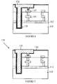
- FIG. 1 is a cross-sectional view of a portion of a stacked integrated circuit 10 according to the present invention.
- FIG. 2 is a cross-sectional view of a wafer 100 used as a starting point for a component layer.
- FIG. 3 is a cross-sectional view of wafer 100 after a via 120 has been etched through the dielectric layers and into substrate 110 .
- FIG. 4 is a cross-sectional view of wafer 100 after via 120 has been lined with two layers.
- FIG. 5 is a cross-sectional view of wafer 100 after a trench 128 has been etched in dielectric layer 116 .
- FIG. 6 illustrates a copper pad that is flush with the surrounding dielectric after the excess copper has been removed by chemical mechanical polishing (CMP).
- CMP chemical mechanical polishing
- FIG. 7 is a cross-sectional view of a completed component layer element 135 .
- FIG. 8 is a cross-sectional view of a base component layer element 202 positioned relative to a component layer element 201 that is to be bonded to element 202 .
- FIG. 9 is a cross-sectional view of the component layers after component layer element 202 has been thinned.
- FIG. 10 is a cross-sectional view of component layer 135 shown in FIG. 7 after a socket 282 has been formed from a SiO 2 layer 281 .
- FIG. 11 is a cross-sectional view of component layer 135 shown in FIG. 7 after socket 261 has been etched.
- FIG. 12 is a cross-sectional view of a portion of a component wafer.
- FIG. 1 is a cross-sectional view of a portion of a stacked integrated circuit 10 according to the present invention having a base component layer 20 and two stacked component layers shown at 30 and 40 .
- Each component layer includes an integrated circuit layer that is constructed on a substrate using conventional integrated circuit fabrication techniques. To simplify the following discussion, it will be assumed that the integrated circuit layer is constructed on a conventional silicon substrate in the form of a wafer.
- the integrated circuit layers corresponding to component layers 20 , 30 , and 40 are shown at 22 , 32 , and 42 , respectively.
- the substrates on which these layers were constructed are shown at 21 , 31 , and 41 , respectively.
- the integrated circuit layer is covered with one or more layers of dielectric such as SiO 2 in which various metal conductors are constructed and connected to the circuitry by vias.
- dielectric such as SiO 2
- various metal conductors are constructed and connected to the circuitry by vias.
- Exemplary conductors of this type are shown at 25 , 35 , and 45 together with the dielectric layers that are shown at 23 , 33 , and 43 .
- Connections between the various component layers are provided by vertical conductors that pass through one or more component layers.
- a typical vertical conductor is shown at 50 .
- Vertical conductor 50 is constructed from component conductors shown at 51 - 53 by thermal diffusion bonding of the component conductors. The thermal diffusion bonding of the component conductors also bonds the various component layers together.
- the diameters of the vias are preferably as small as possible.
- the minimum diameter of a via is determined by the aspect ratio permitted by the metallization process used to fill the via. Vias with aspect ratios of greater than 5 are difficult to fill reliability.
- thin component layers are more flexible. The flexibility improves the strength of the stacked structure and reduces cracking or other damage caused by thermal stress.
- a stacked integrated circuit according to the present invention is constructed by bonding wafer-sized component layers. After all of the layers have bonded, the stacked structure is then divided into individual stacked chips. If the component layers become wedge shaped or have hills and valleys in the surface thereof due to fabrication errors, the bonding between layers will fail. In addition, the vertical vias will not be properly aligned in some areas of the chip. Hence, any economically practical wafer-stacking scheme must assure a high degree of precision over the entire wafer for each wafer component used. The manner in which the present invention provides this high degree of precision will now be discussed in detail.
- a stacked wafer circuit such as that shown in FIG. 1 is constructed by first bonding wafers 20 and 30 via their front sides, and then bonding successive wafers such as wafer 40 by bonding the front side of the new wafer to the backside of the last wafer in the stack.
- FIG. 2 is a cross-sectional view of a wafer 100 used as a starting point for a component layer.
- wafer 100 has its active circuit layer 112 , which is covered with a dielectric layer 113 , in place.
- various metal conductors are typically constructed in the dielectric layer and connected to the circuitry by metal filled vias.
- Typical metal conductors are shown at 114 and 115 . These conductors can be divided into two classes, those that provide connections between the various components in integrated circuit layer 112 and those that are to provide connections to components in other layers of the final stacked integrated circuit.
- Conductor 115 is in the first class
- conductor 114 is in the second class.
- a second layer of dielectric 116 covers the conductors.
- FIG. 3 is a cross-sectional view of wafer 100 after a via 120 has been etched through the dielectric layers and into substrate 110 .
- the depth 121 by which via 120 extends into substrate 110 is critical.
- via 120 is etched in two steps. In the first step, the via is etched using an etchant that stops on the silicon substrate such as a fluorocarbon-based plasma etch. In the second step, the via is extended into substrate 110 by 4 to 9 microns using a timed halogen-containing gaseous plasma. It should be noted that the placement of the vias can be controlled precisely, since the wafer has fiduciary marks that are visible from the front side of the wafer, and these marks can be used to align the masks that define the via locations using conventional alignment tools.
- FIG. 4 is a cross-sectional view of wafer 100 after via 120 has been lined with two layers.
- Layer 125 consists of a thin dielectric layer, preferably 0.05 to 0.10 microns of SiO 2 . This layer acts as an electrical insulator to prevent shorting between the metal layer of the filled via and components in the integrated circuit layer 112 .
- the second layer 126 consists of a thin layer of SiN, typically 0.05 to 0.10 microns in thickness.
- the SiN layer serves two functions. First, it provides a diffusion barrier that helps to prevent the metal used to fill via 120 from diffusing into the integrated circuit layer if the primary diffusion barrier discussed below fails.
- the silicon nitride provides an etch stop for the chemical etching processes used in the thinning of the silicon wafer.
- the silicon can be thinned using a wet chemical process such as a substituted ammonium hydroxide or other alkaline chemical etches. It should also be noted that this etch stop will provide some resistance to acidic etch solutions.
- the silicon nitride acts as the etch stop. If a dry etch such as a Cl 2 based plasma chemistry is used to thin silicon, the SiO 2 layer can be used as an etch stop.
- FIG. 5 is a cross-sectional view of wafer 100 after a trench 128 has been etched in dielectric layer 116 .
- a via 129 is opened in the bottom of trench 128 to provide contact with pad 117 that provides electrical connection to components in circuit layer 112 that are to be connected to the vertical conductor that will be formed by filling via 120 with metal.
- a third layer 130 is deposited in via 129 and trench 128 .
- Layer 130 serves two functions. First, layer 130 acts as a diffusion barrier that prevents the metal used to filled the via and trench from diffusing into the remainder of the wafer. In the preferred embodiment of the present invention, the preferred metal is copper.
- the diffusion barrier is preferably Ta, TaN, or WN or other ternary barrier material such as Ta x Si y N z , W 2 Si y N z , etc.
- a 200-1000 A° barrier layer is preferably deposited by a CVD or a PVD process such as sputtering.
- the portion of layer 130 at the bottom of via 127 acts as a stop in the wafer thinning process described below. Trench 128 is then filled with metal.
- the preferred metal for the filling operation is copper.
- a copper seed layer is deposited in the trench and vias prior to the deposition of the copper.
- the seed layer can be deposited utilizing a CVD or a sputtering process.
- the seed layer maintains the proper conduction during the subsequent electro-plating process utilized to deposit the metallic copper.
- the trench is filled with copper using electrochemical plating.
- the excess copper is removed by chemical mechanical polishing (CMP), leaving a copper pad that is flush with the surrounding dielectric as shown in FIG. 6.
- CMP chemical mechanical polishing
- the final copper pad 132 is elevated relative to the surrounding dielectric layer 133 by 0.01-0.2 microns as shown in FIG.
- This slightly elevated pad provides improved bonding when the component layer element is bonded as described below.
- the elevation of the pad can be accomplished by lowering the surrounding dielectric layer or by increasing the height of the copper.
- the dielectric layer can be lowered by selective etching using a fluorine containing etch process.
- the copper height can be increased by electroless deposition of additional copper, which will occur only on the exposed copper surface.
- FIG. 8 is a cross-sectional view of a base component layer element 202 positioned relative to a component layer element 201 that is to be bonded to element 202 .
- the elements are positioned by turning element 201 over such that its copper bonding pads are positioned over the corresponding bonding pads on element 202 .
- only one pair of pads is shown at 210 and 211 ; however, it is to be understood that each component element may have thousands or even millions of such pads.
- the two component elements are pressed together and bonded using thermal diffusion bonding.
- the wafers are bonded by compressing the two wafers using 20-60 psi pressure at 300-450° C. temperature in a nitrogen or air atmosphere for 5-50 minutes.
- the wafers are positioned by utilizing fiducial marks on the front sides of the wafers.
- the marks on the front side of wafer 202 are viewed from the backside of the wafer. To improve the accuracy of the alignment, wafer 202 may be thinned prior to bonding.
- element 202 is thinned further to a thickness of a few microns as shown in FIG. 9 which is a cross-sectional view of the component layers after component layer element 202 has been thinned.
- the resulting layer component must have parallel surfaces to assure that any subsequent element bonded to this element will be properly aligned and bonded.
- the portion of the diffusion/stop layer shown at 130 in FIG. 5 in the bottom of the vertical vias is used as a stop for this thinning process.
- the preferred thinning process utilizes CMP of the substrate 203 .
- the thinning process can be a combination of grinding and CMP and/or etch processes.
- a CMP process will remove the silicon substrate at a rate that is 100 times faster than Ta in layer 130 . Hence, the CMP process will stop at the same point on each of the vias.
- the depth of the vias can be controlled to a high degree of precision. Hence, the resulting component layer will have a thickness that is tightly controlled, since it is determined by the depth of the vias.
- the silicon substrate is etched faster than the metal filled vias; hence, when the thinning process is completed, the end of the metal via 252 is elevated relative to the surface 253 of substrate 203 . At this point, no further processing of the backside of wafer 202 is required.
- the stacking process can be continued by connecting pads on the front side of another wafer to the elevated posts on the backside of the last wafer that was added to the stack.
- a “socket” is provided on the front side of each new wafer.
- the sockets engage the elevated “posts” described above.
- the sockets can be generated by any of a number of methods. One such method is illustrated in FIG. 10, which is a cross-sectional view of component layer 135 shown in FIG. 7 after a socket 282 has been formed from a SiO 2 layer 281 .
- the thin layer of SiO 2 can be deposited over the front side of the next wafer by conventional techniques and a via opened in the layer to form the socket.
- the thickness of the SiO 2 layer must be less than the height with which conductor 252 extends over substrate 253 .
- the depression that forms the socket can also be generated by etching a depression 261 in the metal pad 262 on the front side of the component wafer as shown in FIG. 11, which is a cross-sectional view of component layer 135 shown in FIG. 7 after socket 261 has been etched.
- the etch area can be set by conventional masking operations.
- the depth of the depression should be less than the height with which conductor 252 extends over substrate 253 .
- the wafer is positioned over the backside of the last wafer in the stack and bonded thereto as described above.
- the positioning operation preferably utilizes a new front-side fiducial mark that is generated using the filled vias as references.
- the filled vias can be used as fiducial marks.
- the new component element is thinned as described above. This process may be continued with additional component elements until the desired stack thickness is obtained.
- the above-described embodiments of the present invention utilize a socket that mates with the extended post on the backside of the last component layer in the stack.
- the socket provides additional resistance to lateral stress such as that generated in the thinning operations. However, if there are a sufficient number of binding sites between the component wafers, this additional stress resistance is not needed. In such cases, the extended posts can be bonded directly to the metal pads on the front side of the next wafer to be added.
- the above-described embodiments of the present invention have utilized vertical conductors that serve both as bonding points between the component wafers and also as signal or power conduction paths that run vertically through the stack.
- the distance between vias is less than 50 ⁇ M and the wafers are thinned to a thickness of 1 to 25 ⁇ M.
- bonding points are preferably similar to those used for vertical conduction paths. However, since these bonding pads do not need to connect to the internal conductors in the component wafers, the lateral extent of such pads may be substantially less.
- a typical bonding point is shown at 280 in FIG. 12, which is a cross-sectional view of a portion of a component wafer.
- the bonding points that hold the various component wafers together extend through the component wafers.
- This arrangement provides a significant improvement in the stress levels that can be accommodated by the bonded wafers.
- prior art schemes that utilize metal pads that are deposited on the opposing surfaces of the bonded layers provide less resistance to lateral stresses.
- the area of the pads must be substantially increased. However, this can led to “peeling” of the pads off of the surface of the wafers because of the different thermal expansion coefficients of the pads and the underlying silicon.
Abstract
An integrated circuit wafer element and an improved method for bonding the same to produce a stacked integrated circuit. Plugs that extend from one surface of the wafer into the wafer are used to provide vertical connections and to bond the wafers together. A stacked integrated circuit is constructed by bonding the front side of a new wafer to a wafer in the stack and then thinning the backside of the new wafer to a thickness that leaves a portion of the plugs extending above the surface of the backside of the thinned wafer. The elevated plug ends can then be used to bond another wafer by bonding to pads on the front side of that wafer. The mating bonding pads can include depressed regions that mate to the elevated plug ends.
Description
- The present invention relates to integrated circuits, and more particularly, to a method for bonding wafers together to form integrated circuits having a stack of thin layers.
- Modem integrated circuits are typically constructed in a thin layer in a semiconducting layer on a substrate wafer such as silicon. This essentially two-dimensional structure limits both the size of the integrated circuit and the speed at which the circuit operates. The speed at which an integrated circuit operates is determined by the distance between the farthest separated components that must communicate with one another on the chip. For any given number of components, the path lengths will, in general, be significantly reduced if the circuit can be laid out as a three dimensional structure consisting of a number of vertically-stacked layers of circuitry, provided the vertical distances between the layers are much smaller than the width of the chips that make up the individual layers.
- One promising scheme for providing such stacked structures utilizes a method for stacking and bonding entire wafers. In this method, integrated circuits are fabricated on conventional wafers. Two wafers are bonded vertically by thinning one wafer in a first coarse thinning operation by removing material from the back of the wafer. The circuitry on the front surface of each wafer is covered with an insulating layer having metal filled vias that make contact with the underlying circuitry and act as electrical connection points between the two wafers. In addition, the front surfaces of the wafers include bonding pads that are planar metal areas that do not connect to the underlying circuitry. The bonding pads are provided to increase the bonded area. The front surfaces of the wafers are then placed in contact with one another so that the bonding pads on one wafer are in contact with the pads on the other wafer. Thermal diffusion bonding is then used to bond the metal pads, and hence, the wafers together. One of the wafers is then further thinned to a thickness of a few microns by etching or mechanically grinding the back surface of that wafer further. Once the wafer has been thinned, a new set of vias is opened in the backside and filled with metal to provide the connection points to the pads on the front side of the wafer that make connections with the circuitry in the wafer. In addition, a new set of bonding pads is formed on the backside of the wafer so that another wafer can be bonded to the stack. The process is then repeated until the desired number of layers has been bonded to form the three-dimensional stack. The three-dimensional stack is then cut into three-dimensional chips and packaged.
- Each time a top wafer in the stack is thinned, the wafers below that wafer are subjected to a significant amount of lateral stress by the grinding process. Accordingly, the bonds that hold the wafers together must withstand these large stresses. In principle, the ability of the wafers to withstand these stresses can be increased by increasing the bond area, i.e., devoting more area to bonding pads between the wafers. Unfortunately, this approach has the drawback of reducing the number of vertical conductors that can be provided in circuits requiring a high density of inter-layer vertical conductors.
- This process also requires a considerable amount of “backside processing” to provide the new set of contacts on the backside of the wafer. The generation of the vertical conductors requires a number of masking and deposition steps. Each conductor is structurally similar to a golf tee. The “head” of the tee provides the area needed to accommodate alignment errors. Separate mask and deposition steps are required to etch the via that forms the stem of the tee and the head that sits on this stem. The via must also be lined to prevent diffusion of the metal into the surrounding silicon. Such extensive backside processing can substantially reduce the yield of stacked wafers.
- The situation is made more complicated by the lack of fiduciary marks on the backside of the thinned wafer. Hence, precise alignment of the masks that define the locations of the vias with respect to the circuitry on the front side of the wafer is difficult. Misalignment of these vias leads to defects that render the entire stack of chips useless. In addition, the semiconductor processing steps required by the backside processing of the top layer subject the underlying layers to thermal and mechanical stresses that are repeated with each new layer.
- Broadly, it is the object of the present invention to provide an improved method for stacking and thinning wafers to generate a three-dimensional integrated circuit.
- It is a further object of the present invention to provide a method that eliminates the backside processing steps utilized in prior art stacking techniques.
- These and other objects of the present invention will become apparent to those skilled in the art from the following detailed description of the invention and the accompanying drawings.
- An integrated circuit wafer element and an improved method for bonding the same to produce a stacked integrated circuit. An integrated circuit wafer according to the present invention includes a substrate having first and second surfaces constructed from a wafer material, the first surface having a circuit layer that includes integrated circuit elements constructed thereon. A plurality of vias extend from the first surface through the circuit layer and terminate in the substrate at a first distance from the first surface. The vias include a stop layer located in the bottom of each via constructed from a stop material that is more resistant to chemical/mechanical polishing (CMP) than the wafer material. The vias may be filled with an electrically conducting material to provide vertical connections between the various circuit layers in a stacked integrated circuit. In this case, the electrical conducting vias may also be connected to various circuit elements by metallic conductors disposed in a dielectric layer that covers the circuit layer. A plurality of bonding pads are provided on one surface of the integrated circuit wafer. These pads may be part of the conducting plugs resulting from filling the vias with the conducting material. These pads preferably extend above the surface of the integrated circuit wafer. A stacked integrated circuit according to the present invention is constructed by bonding two integrated circuit wafers together utilizing the bonding pads. One of the integrated circuit wafers is then thinned to a predetermined thickness determined by the depth of the vias by chemical/mechanical polishing (CMP) of the surface of that integrated circuit wafer that is not bonded to the other integrated circuit wafer, the stop layer in the vias preventing the CMP from removing wafer material that is within the first distance from the first surface of the substrate of the wafer being thinned. The thinning operation leaves a portion of the plug in the via standing above the surface of the thinned substrate. A third wafer can then be bonded to the raised portion of the plug by bonding the raised portion of the plug to pads on the third wafer's surface. The bonding pads on the third wafer surface preferably include a depressed region for engaging the raised portion of the plugs on the second wafer.
- FIG. 1 is a cross-sectional view of a portion of a stacked integrated
circuit 10 according to the present invention. - FIG. 2 is a cross-sectional view of a
wafer 100 used as a starting point for a component layer. - FIG. 3 is a cross-sectional view of
wafer 100 after avia 120 has been etched through the dielectric layers and intosubstrate 110. - FIG. 4 is a cross-sectional view of
wafer 100 after via 120 has been lined with two layers. - FIG. 5 is a cross-sectional view of
wafer 100 after atrench 128 has been etched indielectric layer 116. - FIG. 6 illustrates a copper pad that is flush with the surrounding dielectric after the excess copper has been removed by chemical mechanical polishing (CMP).
- FIG. 7 is a cross-sectional view of a completed
component layer element 135. - FIG. 8 is a cross-sectional view of a base
component layer element 202 positioned relative to acomponent layer element 201 that is to be bonded toelement 202. - FIG. 9 is a cross-sectional view of the component layers after
component layer element 202 has been thinned. - FIG. 10 is a cross-sectional view of
component layer 135 shown in FIG. 7 after asocket 282 has been formed from a SiO2 layer 281. - FIG. 11 is a cross-sectional view of
component layer 135 shown in FIG. 7 aftersocket 261 has been etched. - FIG. 12 is a cross-sectional view of a portion of a component wafer.
- The manner in which the present invention provides its advantages may be more easily understood with reference to FIG. 1 which is a cross-sectional view of a portion of a stacked
integrated circuit 10 according to the present invention having abase component layer 20 and two stacked component layers shown at 30 and 40. Each component layer includes an integrated circuit layer that is constructed on a substrate using conventional integrated circuit fabrication techniques. To simplify the following discussion, it will be assumed that the integrated circuit layer is constructed on a conventional silicon substrate in the form of a wafer. The integrated circuit layers corresponding to component layers 20, 30, and 40 are shown at 22, 32, and 42, respectively. The substrates on which these layers were constructed are shown at 21, 31, and 41, respectively. The integrated circuit layer is covered with one or more layers of dielectric such as SiO2 in which various metal conductors are constructed and connected to the circuitry by vias. To simplify the drawing, only the metal conductors that are to be connected to components on other component layers are shown in the drawing. Exemplary conductors of this type are shown at 25, 35, and 45 together with the dielectric layers that are shown at 23, 33, and 43. - Connections between the various component layers are provided by vertical conductors that pass through one or more component layers. A typical vertical conductor is shown at 50.
Vertical conductor 50 is constructed from component conductors shown at 51-53 by thermal diffusion bonding of the component conductors. The thermal diffusion bonding of the component conductors also bonds the various component layers together. - It should be noted that, in general, there are thousands, if not tens of thousands, of vertical conductors in a typical stacked integrated circuit. Hence, the diameters of the vias are preferably as small as possible. The minimum diameter of a via is determined by the aspect ratio permitted by the metallization process used to fill the via. Vias with aspect ratios of greater than 5 are difficult to fill reliability. Hence, it is advantageous to have the component layers be as thin as possible. In addition, thin component layers are more flexible. The flexibility improves the strength of the stacked structure and reduces cracking or other damage caused by thermal stress.
- It should also be noted that it is important that the component layers be planar sheets having parallel top and bottom edges. In general, a stacked integrated circuit according to the present invention is constructed by bonding wafer-sized component layers. After all of the layers have bonded, the stacked structure is then divided into individual stacked chips. If the component layers become wedge shaped or have hills and valleys in the surface thereof due to fabrication errors, the bonding between layers will fail. In addition, the vertical vias will not be properly aligned in some areas of the chip. Hence, any economically practical wafer-stacking scheme must assure a high degree of precision over the entire wafer for each wafer component used. The manner in which the present invention provides this high degree of precision will now be discussed in detail.
- For the purposes of the present discussion, the side of a wafer that contains the integrated circuits and conventional metallization layers such as the layers that contain
conductors first bonding wafers wafer 40 by bonding the front side of the new wafer to the backside of the last wafer in the stack. - Refer now to FIG. 2, which is a cross-sectional view of a
wafer 100 used as a starting point for a component layer. It will be assumed thatwafer 100 has itsactive circuit layer 112, which is covered with adielectric layer 113, in place. As noted above, various metal conductors are typically constructed in the dielectric layer and connected to the circuitry by metal filled vias. Typical metal conductors are shown at 114 and 115. These conductors can be divided into two classes, those that provide connections between the various components inintegrated circuit layer 112 and those that are to provide connections to components in other layers of the final stacked integrated circuit.Conductor 115 is in the first class, andconductor 114 is in the second class. It will also be assumed that a second layer ofdielectric 116 covers the conductors. - Refer now to FIG. 3, which is a cross-sectional view of
wafer 100 after a via 120 has been etched through the dielectric layers and intosubstrate 110. As will be explained in more detail below, thedepth 121 by which via 120 extends intosubstrate 110 is critical. Preferably, via 120 is etched in two steps. In the first step, the via is etched using an etchant that stops on the silicon substrate such as a fluorocarbon-based plasma etch. In the second step, the via is extended intosubstrate 110 by 4 to 9 microns using a timed halogen-containing gaseous plasma. It should be noted that the placement of the vias can be controlled precisely, since the wafer has fiduciary marks that are visible from the front side of the wafer, and these marks can be used to align the masks that define the via locations using conventional alignment tools. - Refer now to FIG. 4, which is a cross-sectional view of
wafer 100 after via 120 has been lined with two layers.Layer 125 consists of a thin dielectric layer, preferably 0.05 to 0.10 microns of SiO2. This layer acts as an electrical insulator to prevent shorting between the metal layer of the filled via and components in theintegrated circuit layer 112. Thesecond layer 126 consists of a thin layer of SiN, typically 0.05 to 0.10 microns in thickness. The SiN layer serves two functions. First, it provides a diffusion barrier that helps to prevent the metal used to fill via 120 from diffusing into the integrated circuit layer if the primary diffusion barrier discussed below fails. Second, the silicon nitride provides an etch stop for the chemical etching processes used in the thinning of the silicon wafer. For example, the silicon can be thinned using a wet chemical process such as a substituted ammonium hydroxide or other alkaline chemical etches. It should also be noted that this etch stop will provide some resistance to acidic etch solutions. In this case, the silicon nitride acts as the etch stop. If a dry etch such as a Cl2 based plasma chemistry is used to thin silicon, the SiO2 layer can be used as an etch stop. - Refer now to FIG. 5, which is a cross-sectional view of
wafer 100 after atrench 128 has been etched indielectric layer 116. A via 129 is opened in the bottom oftrench 128 to provide contact withpad 117 that provides electrical connection to components incircuit layer 112 that are to be connected to the vertical conductor that will be formed by filling via 120 with metal. A third layer 130 is deposited in via 129 andtrench 128. Layer 130 serves two functions. First, layer 130 acts as a diffusion barrier that prevents the metal used to filled the via and trench from diffusing into the remainder of the wafer. In the preferred embodiment of the present invention, the preferred metal is copper. The diffusion barrier is preferably Ta, TaN, or WN or other ternary barrier material such as TaxSiyNz, W2 SiyNz, etc. A 200-1000 A° barrier layer is preferably deposited by a CVD or a PVD process such as sputtering. Second, the portion of layer 130 at the bottom of via 127 acts as a stop in the wafer thinning process described below.Trench 128 is then filled with metal. - The preferred metal for the filling operation is copper. In embodiments utilizing copper, a copper seed layer is deposited in the trench and vias prior to the deposition of the copper. The seed layer can be deposited utilizing a CVD or a sputtering process. The seed layer maintains the proper conduction during the subsequent electro-plating process utilized to deposit the metallic copper. After the seed layer is deposited, the trench is filled with copper using electrochemical plating. The excess copper is removed by chemical mechanical polishing (CMP), leaving a copper pad that is flush with the surrounding dielectric as shown in FIG. 6. In the preferred embodiment of the present invention, the
final copper pad 132 is elevated relative to the surroundingdielectric layer 133 by 0.01-0.2 microns as shown in FIG. 7, which is a cross-sectional view of a completedcomponent layer element 135. This slightly elevated pad provides improved bonding when the component layer element is bonded as described below. The elevation of the pad can be accomplished by lowering the surrounding dielectric layer or by increasing the height of the copper. The dielectric layer can be lowered by selective etching using a fluorine containing etch process. The copper height can be increased by electroless deposition of additional copper, which will occur only on the exposed copper surface. - The manner in which the first component layer is added to the base component layer by the front side bonding of two wafers will now be explained in more detail with reference to FIG. 8. FIG. 8 is a cross-sectional view of a base
component layer element 202 positioned relative to acomponent layer element 201 that is to be bonded toelement 202. The elements are positioned by turningelement 201 over such that its copper bonding pads are positioned over the corresponding bonding pads onelement 202. To simplify the drawing, only one pair of pads is shown at 210 and 211; however, it is to be understood that each component element may have thousands or even millions of such pads. The two component elements are pressed together and bonded using thermal diffusion bonding. The wafers are bonded by compressing the two wafers using 20-60 psi pressure at 300-450° C. temperature in a nitrogen or air atmosphere for 5-50 minutes. The wafers are positioned by utilizing fiducial marks on the front sides of the wafers. The marks on the front side ofwafer 202 are viewed from the backside of the wafer. To improve the accuracy of the alignment,wafer 202 may be thinned prior to bonding. - After the two elements have bonded,
element 202 is thinned further to a thickness of a few microns as shown in FIG. 9 which is a cross-sectional view of the component layers aftercomponent layer element 202 has been thinned. As noted above, the resulting layer component must have parallel surfaces to assure that any subsequent element bonded to this element will be properly aligned and bonded. In the preferred embodiment of the present invention, the portion of the diffusion/stop layer shown at 130 in FIG. 5 in the bottom of the vertical vias is used as a stop for this thinning process. The preferred thinning process utilizes CMP of thesubstrate 203. The thinning process can be a combination of grinding and CMP and/or etch processes. For example, a CMP process will remove the silicon substrate at a rate that is 100 times faster than Ta in layer 130. Hence, the CMP process will stop at the same point on each of the vias. The depth of the vias, as noted above, can be controlled to a high degree of precision. Hence, the resulting component layer will have a thickness that is tightly controlled, since it is determined by the depth of the vias. - The silicon substrate is etched faster than the metal filled vias; hence, when the thinning process is completed, the end of the metal via 252 is elevated relative to the
surface 253 ofsubstrate 203. At this point, no further processing of the backside ofwafer 202 is required. - The stacking process can be continued by connecting pads on the front side of another wafer to the elevated posts on the backside of the last wafer that was added to the stack. In the preferred embodiment of the present invention, a “socket” is provided on the front side of each new wafer. The sockets engage the elevated “posts” described above. The sockets can be generated by any of a number of methods. One such method is illustrated in FIG. 10, which is a cross-sectional view of
component layer 135 shown in FIG. 7 after asocket 282 has been formed from a SiO2 layer 281. The thin layer of SiO2 can be deposited over the front side of the next wafer by conventional techniques and a via opened in the layer to form the socket. The thickness of the SiO2 layer must be less than the height with whichconductor 252 extends oversubstrate 253. - The depression that forms the socket can also be generated by etching a
depression 261 in themetal pad 262 on the front side of the component wafer as shown in FIG. 11, which is a cross-sectional view ofcomponent layer 135 shown in FIG. 7 aftersocket 261 has been etched. The etch area can be set by conventional masking operations. Once again, the depth of the depression should be less than the height with whichconductor 252 extends oversubstrate 253. - Once the sockets have been formed in the front surface of the next component wafer to be added to the stack, the wafer is positioned over the backside of the last wafer in the stack and bonded thereto as described above. The positioning operation preferably utilizes a new front-side fiducial mark that is generated using the filled vias as references. Alternatively, the filled vias can be used as fiducial marks.
- After bonding, the new component element is thinned as described above. This process may be continued with additional component elements until the desired stack thickness is obtained.
- The above-described embodiments of the present invention utilize a socket that mates with the extended post on the backside of the last component layer in the stack. The socket provides additional resistance to lateral stress such as that generated in the thinning operations. However, if there are a sufficient number of binding sites between the component wafers, this additional stress resistance is not needed. In such cases, the extended posts can be bonded directly to the metal pads on the front side of the next wafer to be added.
- The above-described embodiments of the present invention have utilized vertical conductors that serve both as bonding points between the component wafers and also as signal or power conduction paths that run vertically through the stack. In addition, there must be a sufficient density of posts in the wafer to provide the etch stop function during the thinning process. If the density of posts is too low, “dishing” can occur in the regions between the posts. In the preferred embodiment of the present invention, the distance between vias is less than 50 μM and the wafers are thinned to a thickness of 1 to 25 μM.
- If the particular integrated circuit design does not provide sufficient vertical conductors to provide enough bonding points to assure that the wafers remain bonded together, additional bonding points can be provided. Such bonding points are preferably similar to those used for vertical conduction paths. However, since these bonding pads do not need to connect to the internal conductors in the component wafers, the lateral extent of such pads may be substantially less. A typical bonding point is shown at 280 in FIG. 12, which is a cross-sectional view of a portion of a component wafer.
- It should be noted that the bonding points that hold the various component wafers together extend through the component wafers. This arrangement provides a significant improvement in the stress levels that can be accommodated by the bonded wafers. For example, prior art schemes that utilize metal pads that are deposited on the opposing surfaces of the bonded layers provide less resistance to lateral stresses. To provide a resistance similar to that provided by the present invention, the area of the pads must be substantially increased. However, this can led to “peeling” of the pads off of the surface of the wafers because of the different thermal expansion coefficients of the pads and the underlying silicon.
- Various modifications to the present invention will become apparent to those skilled in the art from the foregoing description and accompanying drawings. Accordingly, the present invention is to be limited solely by the scope of the following claims.
Claims (17)
1. An integrated circuit wafer comprising:
a wafer comprising a substrate comprising a wafer material, said substrate having first and second surfaces, said first surface having a circuit layer comprising integrated circuit elements constructed thereon;
a plurality of vias extending a first distance from said first surface of said substrate into said substrate, said vias comprising a stop layer comprising a stop material that is more resistant to chemical/mechanical polishing (CMP) than said wafer material; said vias being filled with an electrically conducting material forming a conducting plug extending from said top surface of said substrate into said substrate, said plug having a top portion proximate to said first surface and bottom portion, said top portion having a cross-sectional area that is greater than that of said bottom portion of said plug, wherein said top portion of said plug comprises a recessed region sized to receive an end of a bottom portion of one of said plugs from a second one of said integrated circuit wafers.
2. The integrated circuit wafer of claim 1 wherein said recessed region comprises a via in an insulating layer on said first surface of said substrate.
3. The integrated circuit wafer of claim 1 wherein said recessed region comprises a depression in said plug.
4. The integrated circuit wafer of claim 1 wherein said stop material comprises a material chosen from the group consisting of Ta, TaN, W, WN, TaxSiyNz, W2, and SiyNz, and wherein said wafer material comprises silicon.
5. The integrated circuit wafer of claim 1 wherein said vias are lined with a layer of an electrically insulating material.
6. The integrated circuit wafer of claim 5 wherein said electrically insulating material comprises SiO2.
7. The integrated circuit wafer of claim 5 wherein said vias are filled with an electrically conducting material.
8. The integrated circuit wafer of claim 7 wherein said electrically conducting material comprises an element chosen from the group consisting of copper, tungsten, platinum, and titanium.
9. The integrated circuit wafer of claim 1 further comprising:
a dielectric layer having top and bottom surfaces, said dielectric layer covering said circuit layer such that said bottom surface is in contact with said integrated circuit layer; and
a plurality of electrical conductors buried in said dielectric layer and making electrical connections to said integrated circuit elements.
10. The integrated circuit wafer of claim 9 wherein at least one of said vias extends through said dielectric layer and wherein said one of said vias is filled with an electrically conducting material, said via terminating in an electrically conducting pad on said top surface of said dielectric layer.
11. The integrated circuit wafer of claim 10 wherein said electrically conducting pad extends above said top surface of said dielectric layer.
12. The integrated circuit wafer of claim 10 wherein one of said electrical conductors is connected electrically to said one of said vias.
13. A method for adding a second circuit layer to a first wafer comprising a first circuit layer, said method comprising the steps of:
providing a plurality of bonding pads on a first surface of said first wafer;
providing a second wafer comprising a substrate of a wafer material and said second circuit layer, said second circuit layer being fabricated on a first surface of said substrate and being covered by a layer of dielectric material, said wafer further comprising a plurality of vias extending a predetermined distance from said first surface of said substrate into said substrate, said vias including a layer of stop material, said stop material being more resistant to CMP than said wafer material;
providing a plurality of bonding pads on said second wafer, there being a one to one correspondence between said bonding pads on said first and second wafers;
positioning said first and second wafers such that said bonding pads on said first wafer are brought in contact with said bonding pads on said second wafer;
causing said corresponding bonding pads to bond to one another; and
thinning said second wafer by removing a portion of said second wafer by CMP of the surface of said second wafer that is not bonded to said first wafer, said stop layer in said vias determining the amount of material that is removed, wherein said vias are filled with a conducting material thereby forming a plug extending from said surface of said second wafer having said bonding pads to said stop layer and wherein said step of thinning said second wafer leaves a portion of said plugs elevated above said surface of said second wafer remaining after removing said portion of said second wafer.
14. The method of claim 13 , wherein said stop material comprises a material chosen from the group consisting of Ta, TaN, W, WN and wherein said wafer material comprises silicon.
15. The method of claim 13 further comprising the steps of:
providing a third wafer having bonding pads on one surface thereof, said bonding pads being positioned to engage said portions of said plugs that extend above said surface of said second wafer;
positioning said third wafer relative to said second wafer such that said bonding pads on said third wafer will contact said portions of said plugs that extend over said surface on said second wafer when said second and third layers are brought together; and
bonding a third wafer to said portions of said plugs that extend above said surface of said second wafer.
16. The method of claim 15 wherein said bonding pads on said surface of said third wafer comprise a depressed region sized to engage said elevated portions of said plugs on said surface of said second wafer.
17. The method of claim 15 wherein said step of positioning said third wafer comprises using said positions of said plugs in said second wafer to determine the relative position of said second and third wafers.
Priority Applications (2)
| Application Number | Priority Date | Filing Date | Title |
|---|---|---|---|
| US10/122,084 US6642081B1 (en) | 2002-04-11 | 2002-04-11 | Interlocking conductor method for bonding wafers to produce stacked integrated circuits |
| US10/658,132 US6838774B2 (en) | 2002-04-11 | 2003-09-08 | Interlocking conductor method for bonding wafers to produce stacked integrated circuits |
Applications Claiming Priority (1)
| Application Number | Priority Date | Filing Date | Title |
|---|---|---|---|
| US10/122,084 US6642081B1 (en) | 2002-04-11 | 2002-04-11 | Interlocking conductor method for bonding wafers to produce stacked integrated circuits |
Related Child Applications (1)
| Application Number | Title | Priority Date | Filing Date |
|---|---|---|---|
| US10/658,132 Division US6838774B2 (en) | 2002-04-11 | 2003-09-08 | Interlocking conductor method for bonding wafers to produce stacked integrated circuits |
Publications (2)
| Publication Number | Publication Date |
|---|---|
| US20030193076A1 true US20030193076A1 (en) | 2003-10-16 |
| US6642081B1 US6642081B1 (en) | 2003-11-04 |
Family
ID=28790486
Family Applications (2)
| Application Number | Title | Priority Date | Filing Date |
|---|---|---|---|
| US10/122,084 Expired - Lifetime US6642081B1 (en) | 2002-04-11 | 2002-04-11 | Interlocking conductor method for bonding wafers to produce stacked integrated circuits |
| US10/658,132 Expired - Lifetime US6838774B2 (en) | 2002-04-11 | 2003-09-08 | Interlocking conductor method for bonding wafers to produce stacked integrated circuits |
Family Applications After (1)
| Application Number | Title | Priority Date | Filing Date |
|---|---|---|---|
| US10/658,132 Expired - Lifetime US6838774B2 (en) | 2002-04-11 | 2003-09-08 | Interlocking conductor method for bonding wafers to produce stacked integrated circuits |
Country Status (1)
| Country | Link |
|---|---|
| US (2) | US6642081B1 (en) |
Cited By (41)
| Publication number | Priority date | Publication date | Assignee | Title |
|---|---|---|---|---|
| US20040124513A1 (en) * | 2002-12-19 | 2004-07-01 | Via Technologies, Inc. | High-density multichip module package |
| KR100687420B1 (en) | 2004-12-30 | 2007-02-27 | 동부일렉트로닉스 주식회사 | Stacked semiconductor device and manufacturing method for the same |
| US20080029850A1 (en) * | 2006-08-01 | 2008-02-07 | Qimonda Ag | Electrical through contact |
| US20080108205A1 (en) * | 2003-10-06 | 2008-05-08 | Semiconductor Energy Laboratory Co., Ltd. | Semiconductor device and method for manufacturing the same |
| US20080286899A1 (en) * | 2007-05-18 | 2008-11-20 | Oh-Jin Jung | Method for manufacturing semiconductor device and method for manufacturing system-in-package using the same |
| US20090001602A1 (en) * | 2007-06-26 | 2009-01-01 | Qwan Ho Chung | Stack package that prevents warping and cracking of a wafer and semiconductor chip and method for manufacturing the same |
| US20090115042A1 (en) * | 2004-06-04 | 2009-05-07 | Zycube Co., Ltd. | Semiconductor device having three-dimensional stacked structure and method of fabricating the same |
| US20090149023A1 (en) * | 2004-08-20 | 2009-06-11 | Zycube Co., Ltd. | Method of fabricating semiconductor device having three-dimensional stacked structure |
| US20090224388A1 (en) * | 2008-03-04 | 2009-09-10 | International Business Machines Corporation | Semiconductor chip stacking for redundancy and yield improvement |
| US20090224405A1 (en) * | 2008-03-07 | 2009-09-10 | Taiwan Semiconductor Manufacturing Co., Ltd. | Through via process |
| US20090269888A1 (en) * | 2005-06-14 | 2009-10-29 | John Trezza | Chip-based thermo-stack |
| US20100015732A1 (en) * | 2007-11-29 | 2010-01-21 | International Business Machines Corporation | Semiconductor chip repair by stacking of a base semiconductor chip and a repair semiconductor chip |
| US20100140772A1 (en) * | 2008-12-08 | 2010-06-10 | Stats Chippac, Ltd. | Semiconductor Device and Method of Forming Vertical Interconnect Structure in Substrate for IPD and Baseband Circuit Separated by High-Resistivity Molding Compound |
| US7785987B2 (en) | 2005-06-14 | 2010-08-31 | John Trezza | Isolating chip-to-chip contact |
| US20100219503A1 (en) * | 2005-06-14 | 2010-09-02 | John Trezza | Chip capacitive coupling |
| DE112006000647B4 (en) * | 2005-03-16 | 2010-09-23 | Intel Corporation, Santa Clara | Method for forming self-passivating interconnects |
| US7851348B2 (en) | 2005-06-14 | 2010-12-14 | Abhay Misra | Routingless chip architecture |
| US7884483B2 (en) | 2005-06-14 | 2011-02-08 | Cufer Asset Ltd. L.L.C. | Chip connector |
| KR101040533B1 (en) * | 2008-05-28 | 2011-06-16 | 한국과학기술원 | Semiconductor Device and Manufacturing Method Thereof |
| US8021922B2 (en) | 2005-06-14 | 2011-09-20 | Cufer Asset Ltd. L.L.C. | Remote chip attachment |
| US8084851B2 (en) | 2005-06-14 | 2011-12-27 | Cufer Asset Ltd. L.L.C. | Side stacking apparatus and method |
| US20120248621A1 (en) * | 2011-03-31 | 2012-10-04 | S.O.I.Tec Silicon On Insulator Technologies | Methods of forming bonded semiconductor structures, and semiconductor structures formed by such methods |
| CN102738025A (en) * | 2011-03-31 | 2012-10-17 | Soitec公司 | Method of forming bonded semiconductor structure, and semiconductor structure formed by such method |
| US8456015B2 (en) | 2005-06-14 | 2013-06-04 | Cufer Asset Ltd. L.L.C. | Triaxial through-chip connection |
| TWI411088B (en) * | 2007-06-15 | 2013-10-01 | Micron Technology Inc | Semiconductor assemblies, stacked semiconductor devices, and methods of manufacturing semiconductor assemblies and stacked semiconductor devices |
| CN103367240A (en) * | 2012-04-09 | 2013-10-23 | 南亚科技股份有限公司 | Copper-pollution prevention method in back-thinning process of through silicon via |
| TWI416691B (en) * | 2006-03-30 | 2013-11-21 | Freescale Semiconductor Inc | Barrier for use in 3-d integration of circuits |
| US8637995B2 (en) | 2011-03-31 | 2014-01-28 | Soitec | Bonded semiconductor structures including two or more processed semiconductor structures carried by a common substrate |
| FR3009649A1 (en) * | 2013-08-09 | 2015-02-13 | Commissariat Energie Atomique | INTERCONNECTING MULTIPLE LEVELS OF A STACK OF ELECTRONIC COMPONENT SUPPORTS |
| US20150262890A1 (en) * | 2014-03-11 | 2015-09-17 | Canon Kabushiki Kaisha | Forming method and method of manufacturing article |
| US20150357296A1 (en) * | 2012-10-31 | 2015-12-10 | Taiwan Semiconductor Manufacturing Company, Ltd. | Hybrid bonding mechanisms for semiconductor wafers |
| US20160013134A1 (en) * | 2007-07-31 | 2016-01-14 | Micron Technology, Inc. | Semiconductor devices and methods of manufacturing semiconductor devices |
| US9312229B2 (en) * | 2013-03-15 | 2016-04-12 | Taiwan Semiconductor Manufacturing Company, Ltd. | Hybrid bonding with air-gap structure |
| CN105720067A (en) * | 2010-07-09 | 2016-06-29 | 佳能株式会社 | Solid-state image pickup device |
| DE102005040217B4 (en) * | 2004-08-20 | 2017-02-09 | Kabushiki Kaisha Toshiba | Semiconductor chip manufacturing method, semiconductor device manufacturing method and semiconductor device |
| CN108520858A (en) * | 2018-06-07 | 2018-09-11 | 长江存储科技有限责任公司 | Metal connecting structure and forming method thereof |
| US20190259725A1 (en) * | 2017-07-21 | 2019-08-22 | United Microelectronics Corp. | Manufacturing method of die-stack structure |
| CN112509976A (en) * | 2019-09-13 | 2021-03-16 | 铠侠股份有限公司 | Method for manufacturing semiconductor device |
| US20220246497A1 (en) * | 2020-12-28 | 2022-08-04 | Invensas Bonding Technologies, Inc. | Structures with through-substrate vias and methods for forming the same |
| US20230066256A1 (en) * | 2021-08-30 | 2023-03-02 | Nanya Technology Corporation | Semiconductor device and manufacturing method thereof |
| US11942501B2 (en) | 2009-12-26 | 2024-03-26 | Canon Kabushiki Kaisha | Solid-state image pickup apparatus and image pickup system |
Families Citing this family (112)
| Publication number | Priority date | Publication date | Assignee | Title |
|---|---|---|---|---|
| US7633162B2 (en) * | 2004-06-21 | 2009-12-15 | Sang-Yun Lee | Electronic circuit with embedded memory |
| US6498381B2 (en) * | 2001-02-22 | 2002-12-24 | Tru-Si Technologies, Inc. | Semiconductor structures having multiple conductive layers in an opening, and methods for fabricating same |
| US6867501B2 (en) * | 2001-11-01 | 2005-03-15 | Rohm Co., Ltd. | Semiconductor device and method for manufacturing same |
| US7358116B2 (en) * | 2002-04-29 | 2008-04-15 | Intel Corporation | Substrate conductive post formation |
| US20040102033A1 (en) * | 2002-11-21 | 2004-05-27 | Texas Instruments, Incorporated | Method for forming a ternary diffusion barrier layer |
| US7354798B2 (en) * | 2002-12-20 | 2008-04-08 | International Business Machines Corporation | Three-dimensional device fabrication method |
| US20040124509A1 (en) * | 2002-12-28 | 2004-07-01 | Kim Sarah E. | Method and structure for vertically-stacked device contact |
| JP4072677B2 (en) * | 2003-01-15 | 2008-04-09 | セイコーエプソン株式会社 | Semiconductor chip, semiconductor wafer, semiconductor device and manufacturing method thereof, circuit board, and electronic equipment |
| JP2004221348A (en) * | 2003-01-15 | 2004-08-05 | Seiko Epson Corp | Semiconductor device, its manufacturing method, circuit board and electronic apparatus |
| US6962835B2 (en) | 2003-02-07 | 2005-11-08 | Ziptronix, Inc. | Method for room temperature metal direct bonding |
| TWI231023B (en) * | 2003-05-27 | 2005-04-11 | Ind Tech Res Inst | Electronic packaging with three-dimensional stack and assembling method thereof |
| US7612443B1 (en) * | 2003-09-04 | 2009-11-03 | University Of Notre Dame Du Lac | Inter-chip communication |
| US6821826B1 (en) * | 2003-09-30 | 2004-11-23 | International Business Machines Corporation | Three dimensional CMOS integrated circuits having device layers built on different crystal oriented wafers |
| JP2005175415A (en) * | 2003-12-05 | 2005-06-30 | Taiwan Semiconductor Manufacturing Co Ltd | Integrated circuit device and its manufacturing method |
| US7183653B2 (en) * | 2003-12-17 | 2007-02-27 | Intel Corporation | Via including multiple electrical paths |
| KR100618837B1 (en) * | 2004-06-22 | 2006-09-01 | 삼성전자주식회사 | Method for forming thin wafer stack for wafer level package |
| US7217651B2 (en) * | 2004-07-28 | 2007-05-15 | Intel Corporation | Interconnects with interlocks |
| JP2006041438A (en) * | 2004-07-30 | 2006-02-09 | Shinko Electric Ind Co Ltd | Semiconductor chip built-in substrate, and its manufacturing method |
| US7083425B2 (en) | 2004-08-27 | 2006-08-01 | Micron Technology, Inc. | Slanted vias for electrical circuits on circuit boards and other substrates |
| DE102005001104B3 (en) * | 2005-01-08 | 2006-02-09 | X-Fab Semiconductor Foundries Ag | Electrical method for non destructive testing of the bonding rigidity in semiconductor and other wafers measures expansion of unbonded region |
| KR100782463B1 (en) * | 2005-04-13 | 2007-12-05 | (주)실리콘화일 | Separation type unit pixel of image sensor having 3 dimension structure and manufacture method thereof |
| US7557597B2 (en) | 2005-06-03 | 2009-07-07 | International Business Machines Corporation | Stacked chip security |
| KR100718878B1 (en) * | 2005-06-28 | 2007-05-17 | (주)실리콘화일 | Separation type unit pixel of image sensor having 3 dimension structure and manufacture method thereof |
| US7485968B2 (en) | 2005-08-11 | 2009-02-03 | Ziptronix, Inc. | 3D IC method and device |
| US7358616B2 (en) | 2005-09-14 | 2008-04-15 | Freescale Semiconductor, Inc. | Semiconductor stacked die/wafer configuration and packaging and method thereof |
| TWI287273B (en) * | 2006-01-25 | 2007-09-21 | Advanced Semiconductor Eng | Three dimensional package and method of making the same |
| TWI293499B (en) | 2006-01-25 | 2008-02-11 | Advanced Semiconductor Eng | Three dimensional package and method of making the same |
| KR100743648B1 (en) * | 2006-03-17 | 2007-07-27 | 주식회사 하이닉스반도체 | Method of manufacturing wafer level system in packge |
| US7898095B2 (en) * | 2006-03-20 | 2011-03-01 | Tezzaron Semiconductor, Inc. | Fiducial scheme adapted for stacked integrated circuits |
| US7670927B2 (en) * | 2006-05-16 | 2010-03-02 | International Business Machines Corporation | Double-sided integrated circuit chips |
| US8013342B2 (en) * | 2007-11-14 | 2011-09-06 | International Business Machines Corporation | Double-sided integrated circuit chips |
| KR100837269B1 (en) * | 2006-05-22 | 2008-06-11 | 삼성전자주식회사 | Wafer Level Package And Method Of Fabricating The Same |
| US7385283B2 (en) * | 2006-06-27 | 2008-06-10 | Taiwan Semiconductor Manufacturing Co., Ltd. | Three dimensional integrated circuit and method of making the same |
| KR101043484B1 (en) | 2006-06-29 | 2011-06-23 | 인텔 코포레이션 | Apparatus, system, and method for wireless connection in integrated circuit packages |
| US7750488B2 (en) * | 2006-07-10 | 2010-07-06 | Tezzaron Semiconductor, Inc. | Method for bonding wafers to produce stacked integrated circuits |
| US8241995B2 (en) | 2006-09-18 | 2012-08-14 | International Business Machines Corporation | Bonding of substrates including metal-dielectric patterns with metal raised above dielectric |
| JP5179046B2 (en) * | 2006-11-22 | 2013-04-10 | 新光電気工業株式会社 | Electronic component and method for manufacturing electronic component |
| US7879711B2 (en) * | 2006-11-28 | 2011-02-01 | Taiwan Semiconductor Manufacturing Co., Ltd. | Stacked structures and methods of fabricating stacked structures |
| US8034409B2 (en) * | 2006-12-20 | 2011-10-11 | Lam Research Corporation | Methods, apparatuses, and systems for fabricating three dimensional integrated circuits |
| US8207589B2 (en) | 2007-02-15 | 2012-06-26 | Semiconductor Energy Laboratory Co., Ltd. | Photoelectric conversion device and electronic device, and method for manufacturing photoelectric conversion device |
| TWI331391B (en) * | 2007-03-20 | 2010-10-01 | Siliconware Precision Industries Co Ltd | Stackable semiconductor device and fabrication method thereof |
| TWI349318B (en) * | 2007-04-11 | 2011-09-21 | Siliconware Precision Industries Co Ltd | Stackable semiconductor device and manufacturing method thereof |
| TWI330868B (en) * | 2007-04-13 | 2010-09-21 | Siliconware Precision Industries Co Ltd | Semiconductor device and manufacturing method thereof |
| TW200842998A (en) * | 2007-04-18 | 2008-11-01 | Siliconware Precision Industries Co Ltd | Semiconductor device and manufacturing method thereof |
| TWI331371B (en) * | 2007-04-19 | 2010-10-01 | Siliconware Precision Industries Co Ltd | Semiconductor device and manufacturing method thereof |
| US8134235B2 (en) * | 2007-04-23 | 2012-03-13 | Taiwan Semiconductor Manufacturing Co., Ltd. | Three-dimensional semiconductor device |
| US8586465B2 (en) * | 2007-06-07 | 2013-11-19 | United Test And Assembly Center Ltd | Through silicon via dies and packages |
| US7939941B2 (en) | 2007-06-27 | 2011-05-10 | Taiwan Semiconductor Manufacturing Company, Ltd. | Formation of through via before contact processing |
| KR101374338B1 (en) | 2007-11-14 | 2014-03-14 | 삼성전자주식회사 | semicondoctor device having through-via and method of forming the same |
| US7843064B2 (en) * | 2007-12-21 | 2010-11-30 | Taiwan Semiconductor Manufacturing Company, Ltd. | Structure and process for the formation of TSVs |
| US7872357B2 (en) * | 2008-03-05 | 2011-01-18 | Taiwan Semiconductor Manufacturing Company, Ltd. | Protection for bonding pads and methods of formation |
| US8101996B2 (en) * | 2008-04-15 | 2012-01-24 | Fairchild Semiconductor Corporation | Three-dimensional semiconductor device structures and methods |
| US8853830B2 (en) * | 2008-05-14 | 2014-10-07 | Taiwan Semiconductor Manufacturing Company, Ltd. | System, structure, and method of manufacturing a semiconductor substrate stack |
| US7968460B2 (en) | 2008-06-19 | 2011-06-28 | Micron Technology, Inc. | Semiconductor with through-substrate interconnect |
| FR2928225A1 (en) * | 2008-07-31 | 2009-09-04 | Commissariat Energie Atomique | Producing microelectronic device comprises producing device comprising first substrate, first set of components forming first circuit and second set of components forming second circuit, and producing interconnections between the circuits |
| US8278152B2 (en) * | 2008-09-08 | 2012-10-02 | Taiwan Semiconductor Manufacturing Company, Ltd. | Bonding process for CMOS image sensor |
| US7965329B2 (en) * | 2008-09-09 | 2011-06-21 | Omnivision Technologies, Inc. | High gain read circuit for 3D integrated pixel |
| US20100065949A1 (en) * | 2008-09-17 | 2010-03-18 | Andreas Thies | Stacked Semiconductor Chips with Through Substrate Vias |
| US8653648B2 (en) * | 2008-10-03 | 2014-02-18 | Taiwan Semiconductor Manufacturing Company, Ltd. | Zigzag pattern for TSV copper adhesion |
| US8030780B2 (en) | 2008-10-16 | 2011-10-04 | Micron Technology, Inc. | Semiconductor substrates with unitary vias and via terminals, and associated systems and methods |
| US8053900B2 (en) * | 2008-10-21 | 2011-11-08 | Taiwan Semiconductor Manufacturing Company, Ltd. | Through-substrate vias (TSVs) electrically connected to a bond pad design with reduced dishing effect |
| FR2938970A1 (en) * | 2008-11-26 | 2010-05-28 | St Microelectronics Rousset | METHOD FOR STACKING AND INTERCONNECTING INTEGRATED CIRCUITS |
| US8513119B2 (en) * | 2008-12-10 | 2013-08-20 | Taiwan Semiconductor Manufacturing Company, Ltd. | Method of forming bump structure having tapered sidewalls for stacked dies |
| US20100171197A1 (en) * | 2009-01-05 | 2010-07-08 | Hung-Pin Chang | Isolation Structure for Stacked Dies |
| DE102009004725A1 (en) * | 2009-01-15 | 2010-07-29 | Austriamicrosystems Ag | Through-hole semiconductor circuit and method of manufacturing vertically integrated circuits |
| US8691664B2 (en) * | 2009-04-20 | 2014-04-08 | Taiwan Semiconductor Manufacturing Company, Ltd. | Backside process for a substrate |
| US9799562B2 (en) | 2009-08-21 | 2017-10-24 | Micron Technology, Inc. | Vias and conductive routing layers in semiconductor substrates |
| US8791549B2 (en) * | 2009-09-22 | 2014-07-29 | Taiwan Semiconductor Manufacturing Company, Ltd. | Wafer backside interconnect structure connected to TSVs |
| US8647925B2 (en) * | 2009-10-01 | 2014-02-11 | Taiwan Semiconductor Manufacturing Company, Ltd. | Surface modification for handling wafer thinning process |
| US8482132B2 (en) * | 2009-10-08 | 2013-07-09 | International Business Machines Corporation | Pad bonding employing a self-aligned plated liner for adhesion enhancement |
| US8859390B2 (en) * | 2010-02-05 | 2014-10-14 | International Business Machines Corporation | Structure and method for making crack stop for 3D integrated circuits |
| US8907457B2 (en) | 2010-02-08 | 2014-12-09 | Micron Technology, Inc. | Microelectronic devices with through-substrate interconnects and associated methods of manufacturing |
| US8222139B2 (en) | 2010-03-30 | 2012-07-17 | Taiwan Semiconductor Manufacturing Company, Ltd. | Chemical mechanical polishing (CMP) processing of through-silicon via (TSV) and contact plug simultaneously |
| US8466059B2 (en) | 2010-03-30 | 2013-06-18 | Taiwan Semiconductor Manufacturing Company, Ltd. | Multi-layer interconnect structure for stacked dies |
| US9293366B2 (en) * | 2010-04-28 | 2016-03-22 | Taiwan Semiconductor Manufacturing Company, Ltd. | Through-substrate vias with improved connections |
| JP5517800B2 (en) | 2010-07-09 | 2014-06-11 | キヤノン株式会社 | Member for solid-state imaging device and method for manufacturing solid-state imaging device |
| JP5870493B2 (en) * | 2011-02-24 | 2016-03-01 | セイコーエプソン株式会社 | Semiconductor devices, sensors and electronic devices |
| FR2972565A1 (en) * | 2011-03-09 | 2012-09-14 | Commissariat Energie Atomique | PROCESS FOR PRODUCING VERTICAL INTERCONNECTS THROUGH LAYERS |
| US8900994B2 (en) | 2011-06-09 | 2014-12-02 | Taiwan Semiconductor Manufacturing Company, Ltd. | Method for producing a protective structure |
| US8525168B2 (en) * | 2011-07-11 | 2013-09-03 | International Business Machines Corporation | Integrated circuit (IC) test probe |
| CN103094187B (en) * | 2011-10-31 | 2015-01-21 | 中芯国际集成电路制造(上海)有限公司 | Forming method for silicon through hole |
| KR101870155B1 (en) | 2012-02-02 | 2018-06-25 | 삼성전자주식회사 | Via Connection Structures and Semiconductor Devices Having the Same, and methods of Fabricating the Sames |
| US9768132B2 (en) * | 2012-03-14 | 2017-09-19 | Taiwan Semiconductor Manufacturing Company, Ltd. | Semiconductor structure and method of forming the same |
| CN103545275B (en) * | 2012-07-12 | 2016-02-17 | 中芯国际集成电路制造(上海)有限公司 | Silicon through hole encapsulating structure and formation method |
| KR101402750B1 (en) * | 2012-09-26 | 2014-06-11 | (주)실리콘화일 | Separation type unit pixel of image sensor having 3 dimension structure |
| JP6017297B2 (en) * | 2012-12-14 | 2016-10-26 | オリンパス株式会社 | Manufacturing method of semiconductor device |
| US9064937B2 (en) * | 2013-05-30 | 2015-06-23 | International Business Machines Corporation | Substrate bonding with diffusion barrier structures |
| KR102094924B1 (en) | 2013-06-27 | 2020-03-30 | 삼성전자주식회사 | Semiconductor packages having through electrodes and methods for fabricating the same |
| KR102258739B1 (en) | 2014-03-26 | 2021-06-02 | 삼성전자주식회사 | Semiconductor devices having hybrid stacking structures and methods for fabricating the same |
| US9786633B2 (en) | 2014-04-23 | 2017-10-10 | Massachusetts Institute Of Technology | Interconnect structures for fine pitch assembly of semiconductor structures and related techniques |
| WO2016073049A1 (en) * | 2014-08-11 | 2016-05-12 | Massachusetts Institute Of Technology | Semiconductor structures for assembly in multi-layer semiconductor devices including at least one semiconductor structure |
| WO2016118210A2 (en) | 2014-11-05 | 2016-07-28 | Massachusetts Institute Of Technology | Interconnect structures for assembly of multi-layer semiconductor devices |
| WO2017015432A1 (en) | 2015-07-23 | 2017-01-26 | Massachusetts Institute Of Technology | Superconducting integrated circuit |
| US10134972B2 (en) | 2015-07-23 | 2018-11-20 | Massachusetts Institute Of Technology | Qubit and coupler circuit structures and coupling techniques |
| US9953941B2 (en) | 2015-08-25 | 2018-04-24 | Invensas Bonding Technologies, Inc. | Conductive barrier direct hybrid bonding |
| US10242968B2 (en) | 2015-11-05 | 2019-03-26 | Massachusetts Institute Of Technology | Interconnect structure and semiconductor structures for assembly of cryogenic electronic packages |
| US10199553B1 (en) | 2015-11-05 | 2019-02-05 | Massachusetts Institute Of Technology | Shielded through via structures and methods for fabricating shielded through via structures |
| KR102576349B1 (en) | 2016-08-24 | 2023-09-07 | 삼성전자주식회사 | Image sensor |
| US10381541B2 (en) | 2016-10-11 | 2019-08-13 | Massachusetts Institute Of Technology | Cryogenic electronic packages and methods for fabricating cryogenic electronic packages |
| CN106571334B (en) * | 2016-10-26 | 2020-11-10 | 上海集成电路研发中心有限公司 | Mixed bonding method between silicon wafers |
| US10157867B1 (en) | 2017-08-31 | 2018-12-18 | Taiwan Semiconductor Manufacturing Company, Ltd. | Interconnect structure and method |
| US10840205B2 (en) | 2017-09-24 | 2020-11-17 | Invensas Bonding Technologies, Inc. | Chemical mechanical polishing for hybrid bonding |
| CN107845622B (en) * | 2017-12-04 | 2022-04-08 | 长鑫存储技术有限公司 | Chip stacked body with through-silicon via and manufacturing method thereof |
| US11056348B2 (en) | 2018-04-05 | 2021-07-06 | Invensas Bonding Technologies, Inc. | Bonding surfaces for microelectronics |
| US11393779B2 (en) | 2018-06-13 | 2022-07-19 | Invensas Bonding Technologies, Inc. | Large metal pads over TSV |
| WO2019241417A1 (en) | 2018-06-13 | 2019-12-19 | Invensas Bonding Technologies, Inc. | Tsv as pad |
| US11011494B2 (en) | 2018-08-31 | 2021-05-18 | Invensas Bonding Technologies, Inc. | Layer structures for making direct metal-to-metal bonds at low temperatures in microelectronics |
| US11158573B2 (en) | 2018-10-22 | 2021-10-26 | Invensas Bonding Technologies, Inc. | Interconnect structures |
| KR102626314B1 (en) | 2019-01-28 | 2024-01-17 | 삼성전자주식회사 | Semiconductor device having bonding pads |
| US11315871B2 (en) * | 2019-06-13 | 2022-04-26 | Nanya Technology Corporation | Integrated circuit device with bonding structure and method of forming the same |
| US11049844B2 (en) * | 2019-07-01 | 2021-06-29 | International Business Machines Corporation | Semiconductor wafer having trenches with varied dimensions for multi-chip modules |
| US11264357B1 (en) | 2020-10-20 | 2022-03-01 | Invensas Corporation | Mixed exposure for large die |
Citations (10)
| Publication number | Priority date | Publication date | Assignee | Title |
|---|---|---|---|---|
| US5087585A (en) * | 1989-07-11 | 1992-02-11 | Nec Corporation | Method of stacking semiconductor substrates for fabrication of three-dimensional integrated circuit |
| US5229647A (en) * | 1991-03-27 | 1993-07-20 | Micron Technology, Inc. | High density data storage using stacked wafers |
| US5236118A (en) * | 1992-05-12 | 1993-08-17 | The Regents Of The University Of California | Aligned wafer bonding |
| US5380681A (en) * | 1994-03-21 | 1995-01-10 | United Microelectronics Corporation | Three-dimensional multichip package and methods of fabricating |
| US5627106A (en) * | 1994-05-06 | 1997-05-06 | United Microelectronics Corporation | Trench method for three dimensional chip connecting during IC fabrication |
| US6352923B1 (en) * | 1999-03-01 | 2002-03-05 | United Microelectronics Corp. | Method of fabricating direct contact through hole type |
| US6355501B1 (en) * | 2000-09-21 | 2002-03-12 | International Business Machines Corporation | Three-dimensional chip stacking assembly |
| US6372632B1 (en) * | 2000-01-24 | 2002-04-16 | Taiwan Semiconductor Manufacturing Company | Method to eliminate dishing of copper interconnects by the use of a sacrificial oxide layer |
| US6482677B2 (en) * | 2000-09-25 | 2002-11-19 | Sharp Kabushiki Kaisha | Chip component assembly manufacturing method |
| US6566232B1 (en) * | 1999-10-22 | 2003-05-20 | Seiko Epson Corporation | Method of fabricating semiconductor device |
Family Cites Families (8)
| Publication number | Priority date | Publication date | Assignee | Title |
|---|---|---|---|---|
| US5426072A (en) * | 1993-01-21 | 1995-06-20 | Hughes Aircraft Company | Process of manufacturing a three dimensional integrated circuit from stacked SOI wafers using a temporary silicon substrate |
| US5880010A (en) * | 1994-07-12 | 1999-03-09 | Sun Microsystems, Inc. | Ultrathin electronics |
| US5886877A (en) * | 1995-10-13 | 1999-03-23 | Meiko Electronics Co., Ltd. | Circuit board, manufacturing method therefor, and bump-type contact head and semiconductor component packaging module using the circuit board |
| US6124198A (en) * | 1998-04-22 | 2000-09-26 | Cvc, Inc. | Ultra high-speed chip interconnect using free-space dielectrics |
| US6417094B1 (en) * | 1998-12-31 | 2002-07-09 | Newport Fab, Llc | Dual-damascene interconnect structures and methods of fabricating same |
| US6333560B1 (en) * | 1999-01-14 | 2001-12-25 | International Business Machines Corporation | Process and structure for an interlock and high performance multilevel structures for chip interconnects and packaging technologies |
| US6177347B1 (en) * | 1999-07-02 | 2001-01-23 | Taiwan Semiconductor Manufacturing Company | In-situ cleaning process for Cu metallization |
| US6417087B1 (en) * | 1999-12-16 | 2002-07-09 | Agere Systems Guardian Corp. | Process for forming a dual damascene bond pad structure over active circuitry |
-
2002
- 2002-04-11 US US10/122,084 patent/US6642081B1/en not_active Expired - Lifetime
-
2003
- 2003-09-08 US US10/658,132 patent/US6838774B2/en not_active Expired - Lifetime
Patent Citations (10)
| Publication number | Priority date | Publication date | Assignee | Title |
|---|---|---|---|---|
| US5087585A (en) * | 1989-07-11 | 1992-02-11 | Nec Corporation | Method of stacking semiconductor substrates for fabrication of three-dimensional integrated circuit |
| US5229647A (en) * | 1991-03-27 | 1993-07-20 | Micron Technology, Inc. | High density data storage using stacked wafers |
| US5236118A (en) * | 1992-05-12 | 1993-08-17 | The Regents Of The University Of California | Aligned wafer bonding |
| US5380681A (en) * | 1994-03-21 | 1995-01-10 | United Microelectronics Corporation | Three-dimensional multichip package and methods of fabricating |
| US5627106A (en) * | 1994-05-06 | 1997-05-06 | United Microelectronics Corporation | Trench method for three dimensional chip connecting during IC fabrication |
| US6352923B1 (en) * | 1999-03-01 | 2002-03-05 | United Microelectronics Corp. | Method of fabricating direct contact through hole type |
| US6566232B1 (en) * | 1999-10-22 | 2003-05-20 | Seiko Epson Corporation | Method of fabricating semiconductor device |
| US6372632B1 (en) * | 2000-01-24 | 2002-04-16 | Taiwan Semiconductor Manufacturing Company | Method to eliminate dishing of copper interconnects by the use of a sacrificial oxide layer |
| US6355501B1 (en) * | 2000-09-21 | 2002-03-12 | International Business Machines Corporation | Three-dimensional chip stacking assembly |
| US6482677B2 (en) * | 2000-09-25 | 2002-11-19 | Sharp Kabushiki Kaisha | Chip component assembly manufacturing method |
Cited By (96)
| Publication number | Priority date | Publication date | Assignee | Title |
|---|---|---|---|---|
| US20040124513A1 (en) * | 2002-12-19 | 2004-07-01 | Via Technologies, Inc. | High-density multichip module package |
| US20080108205A1 (en) * | 2003-10-06 | 2008-05-08 | Semiconductor Energy Laboratory Co., Ltd. | Semiconductor device and method for manufacturing the same |
| US7851278B2 (en) * | 2003-10-06 | 2010-12-14 | Semiconductor Energy Laboratory Co., Ltd. | Semiconductor device and method for manufacturing the same |
| US20090115042A1 (en) * | 2004-06-04 | 2009-05-07 | Zycube Co., Ltd. | Semiconductor device having three-dimensional stacked structure and method of fabricating the same |
| DE102005040217B4 (en) * | 2004-08-20 | 2017-02-09 | Kabushiki Kaisha Toshiba | Semiconductor chip manufacturing method, semiconductor device manufacturing method and semiconductor device |
| CN102290425A (en) * | 2004-08-20 | 2011-12-21 | 佐伊科比株式会社 | Method of fabricating semiconductor device having three-dimensional stacked structure |
| US7906363B2 (en) * | 2004-08-20 | 2011-03-15 | Zycube Co., Ltd. | Method of fabricating semiconductor device having three-dimensional stacked structure |
| US20090149023A1 (en) * | 2004-08-20 | 2009-06-11 | Zycube Co., Ltd. | Method of fabricating semiconductor device having three-dimensional stacked structure |
| KR100687420B1 (en) | 2004-12-30 | 2007-02-27 | 동부일렉트로닉스 주식회사 | Stacked semiconductor device and manufacturing method for the same |
| DE112006000647B4 (en) * | 2005-03-16 | 2010-09-23 | Intel Corporation, Santa Clara | Method for forming self-passivating interconnects |
| US7884483B2 (en) | 2005-06-14 | 2011-02-08 | Cufer Asset Ltd. L.L.C. | Chip connector |
| US7942182B2 (en) | 2005-06-14 | 2011-05-17 | Cufer Asset Ltd. L.L.C. | Rigid-backed, membrane-based chip tooling |
| US9324629B2 (en) | 2005-06-14 | 2016-04-26 | Cufer Asset Ltd. L.L.C. | Tooling for coupling multiple electronic chips |
| US9147635B2 (en) | 2005-06-14 | 2015-09-29 | Cufer Asset Ltd. L.L.C. | Contact-based encapsulation |
| US7785987B2 (en) | 2005-06-14 | 2010-08-31 | John Trezza | Isolating chip-to-chip contact |
| US7785931B2 (en) | 2005-06-14 | 2010-08-31 | John Trezza | Chip-based thermo-stack |
| US20100219503A1 (en) * | 2005-06-14 | 2010-09-02 | John Trezza | Chip capacitive coupling |
| US9754907B2 (en) | 2005-06-14 | 2017-09-05 | Cufer Asset Ltd. L.L.C. | Tooling for coupling multiple electronic chips |
| US7808111B2 (en) | 2005-06-14 | 2010-10-05 | John Trezza | Processed wafer via |
| US7847412B2 (en) | 2005-06-14 | 2010-12-07 | John Trezza | Isolating chip-to-chip contact |
| US10340239B2 (en) | 2005-06-14 | 2019-07-02 | Cufer Asset Ltd. L.L.C | Tooling for coupling multiple electronic chips |
| US7851348B2 (en) | 2005-06-14 | 2010-12-14 | Abhay Misra | Routingless chip architecture |
| US8456015B2 (en) | 2005-06-14 | 2013-06-04 | Cufer Asset Ltd. L.L.C. | Triaxial through-chip connection |
| US8846445B2 (en) | 2005-06-14 | 2014-09-30 | Cufer Asset Ltd. L.L.C. | Inverse chip connector |
| US8283778B2 (en) | 2005-06-14 | 2012-10-09 | Cufer Asset Ltd. L.L.C. | Thermally balanced via |
| US7919870B2 (en) | 2005-06-14 | 2011-04-05 | Cufer Asset Ltd. L.L.C. | Coaxial through chip connection |
| US7932584B2 (en) | 2005-06-14 | 2011-04-26 | Cufer Asset Ltd. L.L.C. | Stacked chip-based system and method |
| US20090269888A1 (en) * | 2005-06-14 | 2009-10-29 | John Trezza | Chip-based thermo-stack |
| US7946331B2 (en) | 2005-06-14 | 2011-05-24 | Cufer Asset Ltd. L.L.C. | Pin-type chip tooling |
| US8643186B2 (en) | 2005-06-14 | 2014-02-04 | Cufer Asset Ltd. L.L.C. | Processed wafer via |
| US7969015B2 (en) | 2005-06-14 | 2011-06-28 | Cufer Asset Ltd. L.L.C. | Inverse chip connector |
| US7989958B2 (en) | 2005-06-14 | 2011-08-02 | Cufer Assett Ltd. L.L.C. | Patterned contact |
| US8021922B2 (en) | 2005-06-14 | 2011-09-20 | Cufer Asset Ltd. L.L.C. | Remote chip attachment |
| US8053903B2 (en) | 2005-06-14 | 2011-11-08 | Cufer Asset Ltd. L.L.C. | Chip capacitive coupling |
| US8067312B2 (en) | 2005-06-14 | 2011-11-29 | Cufer Asset Ltd. L.L.C. | Coaxial through chip connection |
| US8232194B2 (en) | 2005-06-14 | 2012-07-31 | Cufer Asset Ltd. L.L.C. | Process for chip capacitive coupling |
| US8084851B2 (en) | 2005-06-14 | 2011-12-27 | Cufer Asset Ltd. L.L.C. | Side stacking apparatus and method |
| US8093729B2 (en) | 2005-06-14 | 2012-01-10 | Cufer Asset Ltd. L.L.C. | Electrically conductive interconnect system and method |
| US8197626B2 (en) | 2005-06-14 | 2012-06-12 | Cufer Asset Ltd. L.L.C. | Rigid-backed, membrane-based chip tooling |
| US8154131B2 (en) | 2005-06-14 | 2012-04-10 | Cufer Asset Ltd. L.L.C. | Profiled contact |
| US8197627B2 (en) | 2005-06-14 | 2012-06-12 | Cufer Asset Ltd. L.L.C. | Pin-type chip tooling |
| TWI416691B (en) * | 2006-03-30 | 2013-11-21 | Freescale Semiconductor Inc | Barrier for use in 3-d integration of circuits |
| US8124521B2 (en) | 2006-08-01 | 2012-02-28 | Qimonda Ag | Electrical through contact |
| JP2008047895A (en) * | 2006-08-01 | 2008-02-28 | Qimonda Ag | Electrical through contact |
| US20080029850A1 (en) * | 2006-08-01 | 2008-02-07 | Qimonda Ag | Electrical through contact |
| US20080286899A1 (en) * | 2007-05-18 | 2008-11-20 | Oh-Jin Jung | Method for manufacturing semiconductor device and method for manufacturing system-in-package using the same |
| TWI411088B (en) * | 2007-06-15 | 2013-10-01 | Micron Technology Inc | Semiconductor assemblies, stacked semiconductor devices, and methods of manufacturing semiconductor assemblies and stacked semiconductor devices |
| US9209166B2 (en) | 2007-06-15 | 2015-12-08 | Micron Technology, Inc. | Semiconductor assemblies, stacked semiconductor devices, and methods of manufacturing semiconductor assemblies and stacked semiconductor devices |
| US8994163B2 (en) | 2007-06-15 | 2015-03-31 | Micron Technology, Inc. | Semiconductor assemblies, stacked semiconductor devices, and methods of manufacturing semiconductor assemblies and stacked semiconductor devices |
| US20090001602A1 (en) * | 2007-06-26 | 2009-01-01 | Qwan Ho Chung | Stack package that prevents warping and cracking of a wafer and semiconductor chip and method for manufacturing the same |
| US20110033980A1 (en) * | 2007-06-26 | 2011-02-10 | Hynix Semiconductor Inc. | Stack package that prevents warping and cracking of a wafer and semiconductor chip and method for manufacturing the same |
| US9711457B2 (en) * | 2007-07-31 | 2017-07-18 | Micron Technology, Inc. | Semiconductor devices with recessed interconnects |
| US9842806B2 (en) | 2007-07-31 | 2017-12-12 | Micron Technology, Inc. | Stacked semiconductor devices |
| US20160013134A1 (en) * | 2007-07-31 | 2016-01-14 | Micron Technology, Inc. | Semiconductor devices and methods of manufacturing semiconductor devices |
| US8679861B2 (en) | 2007-11-29 | 2014-03-25 | International Business Machines Corporation | Semiconductor chip repair by stacking of a base semiconductor chip and a repair semiconductor chip |
| US8796047B2 (en) | 2007-11-29 | 2014-08-05 | International Business Machines Corporation | Semiconductor chip repair by stacking of a base semiconductor chip and a repair semiconductor chip |
| US20100015732A1 (en) * | 2007-11-29 | 2010-01-21 | International Business Machines Corporation | Semiconductor chip repair by stacking of a base semiconductor chip and a repair semiconductor chip |
| US8597960B2 (en) * | 2008-03-04 | 2013-12-03 | International Business Machines Corporation | Semiconductor chip stacking for redundancy and yield improvement |
| US8686559B2 (en) | 2008-03-04 | 2014-04-01 | International Business Machines Corporation | Semiconductor chip stacking for redundancy and yield improvement |
| US20090224388A1 (en) * | 2008-03-04 | 2009-09-10 | International Business Machines Corporation | Semiconductor chip stacking for redundancy and yield improvement |
| US20090224405A1 (en) * | 2008-03-07 | 2009-09-10 | Taiwan Semiconductor Manufacturing Co., Ltd. | Through via process |
| US8486823B2 (en) * | 2008-03-07 | 2013-07-16 | Taiwan Semiconductor Manufacturing Co., Ltd. | Methods of forming through via |
| KR101040533B1 (en) * | 2008-05-28 | 2011-06-16 | 한국과학기술원 | Semiconductor Device and Manufacturing Method Thereof |
| US20100140772A1 (en) * | 2008-12-08 | 2010-06-10 | Stats Chippac, Ltd. | Semiconductor Device and Method of Forming Vertical Interconnect Structure in Substrate for IPD and Baseband Circuit Separated by High-Resistivity Molding Compound |
| US10192801B2 (en) | 2008-12-08 | 2019-01-29 | STATS ChipPAC Pte. Ltd. | Semiconductor device and method of forming vertical interconnect structure in substrate for IPD and baseband circuit separated by high-resistivity molding compound |
| US8168470B2 (en) * | 2008-12-08 | 2012-05-01 | Stats Chippac, Ltd. | Semiconductor device and method of forming vertical interconnect structure in substrate for IPD and baseband circuit separated by high-resistivity molding compound |
| US11942501B2 (en) | 2009-12-26 | 2024-03-26 | Canon Kabushiki Kaisha | Solid-state image pickup apparatus and image pickup system |
| EP3706172A1 (en) * | 2010-07-09 | 2020-09-09 | Canon Kabushiki Kaisha | Solid-state image pickup device |
| US10573680B2 (en) | 2010-07-09 | 2020-02-25 | Canon Kabushiki Kaisha | Solid-state image pickup device |
| US11177310B2 (en) | 2010-07-09 | 2021-11-16 | Canon Kabushiki Kaisha | Solid-state image pickup device |
| CN105720067A (en) * | 2010-07-09 | 2016-06-29 | 佳能株式会社 | Solid-state image pickup device |
| US10217786B2 (en) | 2010-07-09 | 2019-02-26 | Canon Kabushiki Kaisha | Solid-state image pickup device |
| US10553562B2 (en) * | 2011-03-31 | 2020-02-04 | Sony Semiconductor Solutions Corporation | Methods of forming bonded semiconductor structures, and semiconductor structures formed by such methods |
| CN102738025A (en) * | 2011-03-31 | 2012-10-17 | Soitec公司 | Method of forming bonded semiconductor structure, and semiconductor structure formed by such method |
| US8637995B2 (en) | 2011-03-31 | 2014-01-28 | Soitec | Bonded semiconductor structures including two or more processed semiconductor structures carried by a common substrate |
| US20120248621A1 (en) * | 2011-03-31 | 2012-10-04 | S.O.I.Tec Silicon On Insulator Technologies | Methods of forming bonded semiconductor structures, and semiconductor structures formed by such methods |
| US20180012869A1 (en) * | 2011-03-31 | 2018-01-11 | Sony Semiconductor Solutions Corporation | Methods of forming bonded semiconductor structures, and semiconductor structures formed by such methods |
| CN103367240A (en) * | 2012-04-09 | 2013-10-23 | 南亚科技股份有限公司 | Copper-pollution prevention method in back-thinning process of through silicon via |
| US9960129B2 (en) * | 2012-10-31 | 2018-05-01 | Taiwan Semiconductor Manufacturing Company, Ltd. | Hybrid bonding mechanisms for semiconductor wafers |
| US20150357296A1 (en) * | 2012-10-31 | 2015-12-10 | Taiwan Semiconductor Manufacturing Company, Ltd. | Hybrid bonding mechanisms for semiconductor wafers |
| US9443796B2 (en) | 2013-03-15 | 2016-09-13 | Taiwan Semiconductor Manufacturing Company, Ltd. | Air trench in packages incorporating hybrid bonding |
| US9786628B2 (en) | 2013-03-15 | 2017-10-10 | Taiwan Semiconductor Manufacturing Company, Ltd. | Air trench in packages incorporating hybrid bonding |
| US9960142B2 (en) | 2013-03-15 | 2018-05-01 | Taiwan Semiconductor Manufacturing Company, Ltd. | Hybrid bonding with air-gap structure |
| US9502396B2 (en) | 2013-03-15 | 2016-11-22 | Taiwan Semiconductor Manufacturing Company, Ltd. | Air trench in packages incorporating hybrid bonding |
| US9312229B2 (en) * | 2013-03-15 | 2016-04-12 | Taiwan Semiconductor Manufacturing Company, Ltd. | Hybrid bonding with air-gap structure |
| US9312169B2 (en) | 2013-08-09 | 2016-04-12 | Commissariat A L'energie Atomique Et Aux Energies Alternatives | Interconnection of several levels of a stack of supports for electronic components |
| FR3009649A1 (en) * | 2013-08-09 | 2015-02-13 | Commissariat Energie Atomique | INTERCONNECTING MULTIPLE LEVELS OF A STACK OF ELECTRONIC COMPONENT SUPPORTS |
| EP2835824A3 (en) * | 2013-08-09 | 2015-04-29 | Commissariat à l'Énergie Atomique et aux Énergies Alternatives | Interconnection of a plurality of levels of a stack of electronic component media |
| US9564374B2 (en) * | 2014-03-11 | 2017-02-07 | Canon Kabushiki Kaisha | Forming method and method of manufacturing article |
| US20150262890A1 (en) * | 2014-03-11 | 2015-09-17 | Canon Kabushiki Kaisha | Forming method and method of manufacturing article |
| US20190259725A1 (en) * | 2017-07-21 | 2019-08-22 | United Microelectronics Corp. | Manufacturing method of die-stack structure |
| CN108520858A (en) * | 2018-06-07 | 2018-09-11 | 长江存储科技有限责任公司 | Metal connecting structure and forming method thereof |
| CN112509976A (en) * | 2019-09-13 | 2021-03-16 | 铠侠股份有限公司 | Method for manufacturing semiconductor device |
| US20220246497A1 (en) * | 2020-12-28 | 2022-08-04 | Invensas Bonding Technologies, Inc. | Structures with through-substrate vias and methods for forming the same |
| US20230066256A1 (en) * | 2021-08-30 | 2023-03-02 | Nanya Technology Corporation | Semiconductor device and manufacturing method thereof |
| US11749565B2 (en) * | 2021-08-30 | 2023-09-05 | Nanya Technology Corporation | Semiconductor device and manufacturing method thereof |
Also Published As
| Publication number | Publication date |
|---|---|
| US6642081B1 (en) | 2003-11-04 |
| US6838774B2 (en) | 2005-01-04 |
| US20040048459A1 (en) | 2004-03-11 |
Similar Documents
| Publication | Publication Date | Title |
|---|---|---|
| US6838774B2 (en) | Interlocking conductor method for bonding wafers to produce stacked integrated circuits | |
| US20020163072A1 (en) | Method for bonding wafers to produce stacked integrated circuits | |
| US20230005850A1 (en) | Element with routing structure in bonding layer | |
| US7750488B2 (en) | Method for bonding wafers to produce stacked integrated circuits | |
| US9793192B2 (en) | Formation of through via before contact processing | |
| CN101091243B (en) | Single mask via method and device | |
| US7871925B2 (en) | Stack package and method for manufacturing the same | |
| US8970011B2 (en) | Method and structure of forming backside through silicon via connections | |
| US8421238B2 (en) | Stacked semiconductor device with through via | |
| CN112514059A (en) | Interlayer connection of stacked microelectronic components | |
| US6867070B2 (en) | Bonding pad structure of a semiconductor device and method for manufacturing the same | |
| CN102237300B (en) | Through-substrate via and fabrication method thereof | |
| US7786562B2 (en) | Stackable semiconductor chip layer comprising prefabricated trench interconnect vias | |
| CN109390305B (en) | Bonding wafer and preparation method thereof | |
| CN101847597A (en) | Integrated circuit structure | |
| US6677235B1 (en) | Silicon die with metal feed through structure | |
| US6803304B2 (en) | Methods for producing electrode and semiconductor device | |
| CN111769075B (en) | TSV (through silicon via) passive adapter plate for system-in-package and manufacturing method thereof | |
| CN114843247A (en) | Stacked semiconductor device with removable probe pads | |
| JP2001284354A (en) | Method of manufacturing semiconductor device | |
| KR100395907B1 (en) | Method for forming the line of semiconductor device | |
| KR20020060452A (en) | Semiconductor integrated circuit and method for manufacturing the same |
Legal Events
| Date | Code | Title | Description |
|---|---|---|---|
| STCF | Information on status: patent grant |
Free format text: PATENTED CASE |
|
| REMI | Maintenance fee reminder mailed | ||
| FPAY | Fee payment |
Year of fee payment: 4 |
|
| SULP | Surcharge for late payment | ||
| FEPP | Fee payment procedure |
Free format text: PAT HOLDER CLAIMS SMALL ENTITY STATUS, ENTITY STATUS SET TO SMALL (ORIGINAL EVENT CODE: LTOS); ENTITY STATUS OF PATENT OWNER: SMALL ENTITY |
|
| REMI | Maintenance fee reminder mailed | ||
| FPAY | Fee payment |
Year of fee payment: 8 |
|
| SULP | Surcharge for late payment |
Year of fee payment: 7 |
|
| FPAY | Fee payment |
Year of fee payment: 12 |