US20030193623A1 - Array substrate for liquid crystal display device and method of manufacturing the same - Google Patents
Array substrate for liquid crystal display device and method of manufacturing the same Download PDFInfo
- Publication number
- US20030193623A1 US20030193623A1 US10/410,400 US41040003A US2003193623A1 US 20030193623 A1 US20030193623 A1 US 20030193623A1 US 41040003 A US41040003 A US 41040003A US 2003193623 A1 US2003193623 A1 US 2003193623A1
- Authority
- US
- United States
- Prior art keywords
- numbered
- gate
- forming
- shorting bar
- pads
- Prior art date
- Legal status (The legal status is an assumption and is not a legal conclusion. Google has not performed a legal analysis and makes no representation as to the accuracy of the status listed.)
- Granted
Links
Images


Classifications
-
- G—PHYSICS
- G02—OPTICS
- G02F—OPTICAL DEVICES OR ARRANGEMENTS FOR THE CONTROL OF LIGHT BY MODIFICATION OF THE OPTICAL PROPERTIES OF THE MEDIA OF THE ELEMENTS INVOLVED THEREIN; NON-LINEAR OPTICS; FREQUENCY-CHANGING OF LIGHT; OPTICAL LOGIC ELEMENTS; OPTICAL ANALOGUE/DIGITAL CONVERTERS
- G02F1/00—Devices or arrangements for the control of the intensity, colour, phase, polarisation or direction of light arriving from an independent light source, e.g. switching, gating or modulating; Non-linear optics
- G02F1/01—Devices or arrangements for the control of the intensity, colour, phase, polarisation or direction of light arriving from an independent light source, e.g. switching, gating or modulating; Non-linear optics for the control of the intensity, phase, polarisation or colour
- G02F1/13—Devices or arrangements for the control of the intensity, colour, phase, polarisation or direction of light arriving from an independent light source, e.g. switching, gating or modulating; Non-linear optics for the control of the intensity, phase, polarisation or colour based on liquid crystals, e.g. single liquid crystal display cells
- G02F1/133—Constructional arrangements; Operation of liquid crystal cells; Circuit arrangements
- G02F1/136—Liquid crystal cells structurally associated with a semi-conducting layer or substrate, e.g. cells forming part of an integrated circuit
- G02F1/1362—Active matrix addressed cells
- G02F1/136286—Wiring, e.g. gate line, drain line
-
- G—PHYSICS
- G02—OPTICS
- G02F—OPTICAL DEVICES OR ARRANGEMENTS FOR THE CONTROL OF LIGHT BY MODIFICATION OF THE OPTICAL PROPERTIES OF THE MEDIA OF THE ELEMENTS INVOLVED THEREIN; NON-LINEAR OPTICS; FREQUENCY-CHANGING OF LIGHT; OPTICAL LOGIC ELEMENTS; OPTICAL ANALOGUE/DIGITAL CONVERTERS
- G02F1/00—Devices or arrangements for the control of the intensity, colour, phase, polarisation or direction of light arriving from an independent light source, e.g. switching, gating or modulating; Non-linear optics
- G02F1/01—Devices or arrangements for the control of the intensity, colour, phase, polarisation or direction of light arriving from an independent light source, e.g. switching, gating or modulating; Non-linear optics for the control of the intensity, phase, polarisation or colour
- G02F1/13—Devices or arrangements for the control of the intensity, colour, phase, polarisation or direction of light arriving from an independent light source, e.g. switching, gating or modulating; Non-linear optics for the control of the intensity, phase, polarisation or colour based on liquid crystals, e.g. single liquid crystal display cells
- G02F1/133—Constructional arrangements; Operation of liquid crystal cells; Circuit arrangements
- G02F1/1333—Constructional arrangements; Manufacturing methods
- G02F1/1345—Conductors connecting electrodes to cell terminals
- G02F1/13458—Terminal pads
-
- G—PHYSICS
- G02—OPTICS
- G02F—OPTICAL DEVICES OR ARRANGEMENTS FOR THE CONTROL OF LIGHT BY MODIFICATION OF THE OPTICAL PROPERTIES OF THE MEDIA OF THE ELEMENTS INVOLVED THEREIN; NON-LINEAR OPTICS; FREQUENCY-CHANGING OF LIGHT; OPTICAL LOGIC ELEMENTS; OPTICAL ANALOGUE/DIGITAL CONVERTERS
- G02F1/00—Devices or arrangements for the control of the intensity, colour, phase, polarisation or direction of light arriving from an independent light source, e.g. switching, gating or modulating; Non-linear optics
- G02F1/01—Devices or arrangements for the control of the intensity, colour, phase, polarisation or direction of light arriving from an independent light source, e.g. switching, gating or modulating; Non-linear optics for the control of the intensity, phase, polarisation or colour
- G02F1/13—Devices or arrangements for the control of the intensity, colour, phase, polarisation or direction of light arriving from an independent light source, e.g. switching, gating or modulating; Non-linear optics for the control of the intensity, phase, polarisation or colour based on liquid crystals, e.g. single liquid crystal display cells
- G02F1/133—Constructional arrangements; Operation of liquid crystal cells; Circuit arrangements
- G02F1/136—Liquid crystal cells structurally associated with a semi-conducting layer or substrate, e.g. cells forming part of an integrated circuit
- G02F1/1362—Active matrix addressed cells
- G02F1/136254—Checking; Testing
-
- H—ELECTRICITY
- H01—ELECTRIC ELEMENTS
- H01L—SEMICONDUCTOR DEVICES NOT COVERED BY CLASS H10
- H01L27/00—Devices consisting of a plurality of semiconductor or other solid-state components formed in or on a common substrate
- H01L27/02—Devices consisting of a plurality of semiconductor or other solid-state components formed in or on a common substrate including semiconductor components specially adapted for rectifying, oscillating, amplifying or switching and having at least one potential-jump barrier or surface barrier; including integrated passive circuit elements with at least one potential-jump barrier or surface barrier
- H01L27/12—Devices consisting of a plurality of semiconductor or other solid-state components formed in or on a common substrate including semiconductor components specially adapted for rectifying, oscillating, amplifying or switching and having at least one potential-jump barrier or surface barrier; including integrated passive circuit elements with at least one potential-jump barrier or surface barrier the substrate being other than a semiconductor body, e.g. an insulating body
- H01L27/1214—Devices consisting of a plurality of semiconductor or other solid-state components formed in or on a common substrate including semiconductor components specially adapted for rectifying, oscillating, amplifying or switching and having at least one potential-jump barrier or surface barrier; including integrated passive circuit elements with at least one potential-jump barrier or surface barrier the substrate being other than a semiconductor body, e.g. an insulating body comprising a plurality of TFTs formed on a non-semiconducting substrate, e.g. driving circuits for AMLCDs
- H01L27/124—Devices consisting of a plurality of semiconductor or other solid-state components formed in or on a common substrate including semiconductor components specially adapted for rectifying, oscillating, amplifying or switching and having at least one potential-jump barrier or surface barrier; including integrated passive circuit elements with at least one potential-jump barrier or surface barrier the substrate being other than a semiconductor body, e.g. an insulating body comprising a plurality of TFTs formed on a non-semiconducting substrate, e.g. driving circuits for AMLCDs with a particular composition, shape or layout of the wiring layers specially adapted to the circuit arrangement, e.g. scanning lines in LCD pixel circuits
-
- H—ELECTRICITY
- H01—ELECTRIC ELEMENTS
- H01L—SEMICONDUCTOR DEVICES NOT COVERED BY CLASS H10
- H01L27/00—Devices consisting of a plurality of semiconductor or other solid-state components formed in or on a common substrate
- H01L27/02—Devices consisting of a plurality of semiconductor or other solid-state components formed in or on a common substrate including semiconductor components specially adapted for rectifying, oscillating, amplifying or switching and having at least one potential-jump barrier or surface barrier; including integrated passive circuit elements with at least one potential-jump barrier or surface barrier
- H01L27/12—Devices consisting of a plurality of semiconductor or other solid-state components formed in or on a common substrate including semiconductor components specially adapted for rectifying, oscillating, amplifying or switching and having at least one potential-jump barrier or surface barrier; including integrated passive circuit elements with at least one potential-jump barrier or surface barrier the substrate being other than a semiconductor body, e.g. an insulating body
- H01L27/1214—Devices consisting of a plurality of semiconductor or other solid-state components formed in or on a common substrate including semiconductor components specially adapted for rectifying, oscillating, amplifying or switching and having at least one potential-jump barrier or surface barrier; including integrated passive circuit elements with at least one potential-jump barrier or surface barrier the substrate being other than a semiconductor body, e.g. an insulating body comprising a plurality of TFTs formed on a non-semiconducting substrate, e.g. driving circuits for AMLCDs
- H01L27/1259—Multistep manufacturing methods
- H01L27/1288—Multistep manufacturing methods employing particular masking sequences or specially adapted masks, e.g. half-tone mask
-
- H—ELECTRICITY
- H01—ELECTRIC ELEMENTS
- H01L—SEMICONDUCTOR DEVICES NOT COVERED BY CLASS H10
- H01L2924/00—Indexing scheme for arrangements or methods for connecting or disconnecting semiconductor or solid-state bodies as covered by H01L24/00
- H01L2924/0001—Technical content checked by a classifier
- H01L2924/0002—Not covered by any one of groups H01L24/00, H01L24/00 and H01L2224/00
Definitions
- the present invention relates to a liquid crystal display (LCD) device and more particularly, to an array substrate for a liquid crystal display device and a manufacturing method thereof.
- LCD liquid crystal display
- a liquid crystal display (LCD) device includes two substrates that are spaced apart and face each other with a liquid crystal material layer interposed between the two substrates.
- Each of the substrates includes electrodes that face each other, wherein a voltage applied to each electrode induces an electric field between the electrodes and within the liquid crystal material layer. Alignment of liquid crystal molecules of the liquid crystal material layer is changed by varying an intensity or direction of the applied electric field. Accordingly, the LCD device displays an image by varying light transmissivity through the liquid crystal material layer in accordance with the arrangement of the liquid crystal molecules.
- FIG. 1 is an enlarged perspective view of a liquid crystal display (LCD) device according to the related art.
- an LCD device 7 has upper and lower substrates 5 and 9 , which are spaced apart from and facing each other, and a liquid crystal material layer 90 interposed between the upper and lower substrates 5 and 9 .
- the upper substrate 5 includes a black matrix 2 , a color filter layer 1 , and a transparent common electrode 18 subsequently disposed on an interior surface thereof.
- the black matrix 2 includes openings having one of three sub-color filters of red (R), green (G), and blue (B).
- a gate line 11 and a data line 36 are formed on an interior surface of the lower substrate 9 , which is commonly referred to as an array substrate, such that the gate line 11 and the date line 36 cross each other to define a pixel area P.
- a thin film transistor T is formed at the crossing of the gate line 11 and the data line 36 and includes a gate electrode, a source electrode, and a drain electrode.
- a pixel electrode 53 is formed within the pixel area P to correspond to the sub-color filters (R), (G), and (B), and is electrically connected to the thin film transistor T.
- the pixel electrode 53 is made of a light transparent conductive material, such as indium-tin-oxide (ITO).
- a scanning pulse is supplied to the gate electrode of the thin film transistor T along the gate line 11 , and a data signal is supplied to the source electrode of the thin film transistor T along the data line 36 .
- the liquid crystal material layer 90 includes a dielectric anisotropic material having spontaneous polarization properties such that the liquid crystal molecules form a dipole when the electric field is induced.
- the liquid crystal molecules of the liquid crystal material layer 90 are controlled by the applied electric field.
- optical modulation of the liquid crystal material layer 90 is adjusted according to the arrangement of the liquid crystal molecules. Therefore, images of the LCD device are produced by controlling light transmittance of the liquid crystal material layer 90 due to optical modulation of the liquid crystal material layer 90 .
- FIG. 2 is a plan view of an array substrate for an LCD device according to the related art
- FIG. 3 is an enlarged plan view of region “A” of FIG. 2 according to the related art
- FIG. 4 is an enlarged plan view of region “B” of FIG. 2 according to the related art
- FIG. 5 is an enlarged plan view of region “C” of FIG. 2 according to the related art.
- gate lines 11 and data lines 36 are formed on a substrate 9 to cross each other, thereby defining pixel areas P.
- a thin film transistor T (in FIG. 5) is formed at the crossing of each of the gate and data lines 11 and 36 to function as a switching element.
- the thin film transistor T includes a gate electrode 13 that is connected to the gate line 11 to receive scanning signals, a source electrode 33 is connected to the data line 36 and receives data signals, and a drain electrode 35 is spaced apart from the source electrode 33 .
- the thin film transistor T includes an active layer 49 between the gate electrode 13 and the source and drain electrodes 33 and 35 , and a transparent pixel electrode 53 is formed in the pixel area P and is connected to the drain electrode 35 .
- a gate pad 15 is formed at one end of the gate line 11 , and a gate pad terminal 60 overlaps the gate pad 15 .
- the gate pad terminal 60 may be formed of the same material as the pixel electrode 53 .
- the gate pad 15 includes odd and even gate pads 15 a and 15 b , wherein the odd gate pad 15 a is connected to a first shorting bar 17 and the even gate pad 15 b is connected to a second shorting bar 37 .
- a data pad 38 is formed at one end of the data line 36 , and a data pad terminal 62 overlaps the data pad 38 .
- the data pad terminal 62 may be formed of the same material as the pixel electrode 53 .
- the data pad 38 also includes odd and even data pads 38 a and 38 b , wherein the odd data pad 38 a is connected to a third shorting bar 19 and the even data pad 38 b is connected to a fourth shorting bar 39 .
- the first to fourth shorting bars 17 , 37 , 19 , and 39 are electrically connected to first, second, third, and fourth test pads 21 , 41 , 23 and 43 (in FIG. 2) through first, second, third, and fourth connecting lines 20 , 45 , 25 and 47 (in FIG. 2), respectively.
- the first, second, third, and fourth test pads 21 , 41 , 23 , and 43 are formed along a line on a portion of the substrate 9 .
- the first and third shorting bars 17 and 19 are made of the same material as the gate line 11
- the second and fourth shorting bars 37 and 39 are formed of the same material as the data line 36 .
- the first and third test pads 21 and 23 are made of the same material as the gate line 11
- the first and third connecting lines 20 and 25 are formed of the same material as the data line 36 .
- the even gate pad 15 b is electrically connected to the second shorting bar 37 through the gate pad terminal 60
- the even data pad 38 b is electrically connected to the fourth shorting bar 39 through the data pad terminal 62 .
- the shorting bars 17 , 37 , 19 , and 39 are removed by cutting the substrate 9 after the testing process of the array substrate.
- FIGS. 6A to 6 F are cross sectional views of a manufacturing method of the array substrate using four masks along VI-VI of FIG. 5 according to the related art
- FIGS. 7A to 7 F are cross sectional views of a manufacturing method of the array substrate using four masks along VII-VII of FIG. 2 according to the related art.
- a gate electrode 13 is formed on a substrate 9 by depositing a first metal layer, and patterning the first metal layer through a first mask process.
- a gate line 11 in FIG. 5
- a gate pad 15 in FIG. 3
- a gate insulating layer 29 an amorphous silicon layer 30 , a doped amorphous silicon layer 31 , and a second metal layer 32 are subsequently deposited on the substrate 9 and the gate electrode 13 .
- a photoresist layer 70 is formed on the second metal layer 32 by coating a photoresist material.
- the gate insulating layer 29 is made of an inorganic insulating material, such as silicon nitride (SiNx) and silicon oxide (SiO2), and the second metal layer 32 may be formed of chromium (Cr) or molybdenum (Mo).
- a mask 80 includes a blocking portion M 1 , a half transmitting portion M 2 , and a transmitting portion M 3 that are disposed over the photoresist layer 70 , wherein the blocking portion M 1 corresponds to a source drain region D and the half transmitting portion M 2 corresponds to a channel region E.
- the photoresist layer 70 may be a positive type, wherein a portion exposed to light is developed and removed. Subsequently, the photoresist layer 70 is exposed to light such that the portion of the photoresist layer 70 corresponding to the half transmitting portion M 2 is exposed to the light in an amount less than the photoresist layer 70 corresponding to the transmitting portion M 3 .
- the half transmitting portion M 2 may include slits or semitransparent layer.
- FIGS. 6C and 7C the exposed photoresist layer 70 (in FIGS. 6B and 7B) is developed, whereby a photoresist pattern 72 having different thicknesses is formed.
- a first thickness photoresist pattern 72 a corresponds to the blocking portion M 1 (in FIGS. 6B and 7B) and a second thickness photoresist pattern 72 b , which is thinner than the first thickness 72 a , corresponds to the half transmitting portion M 2 (in FIG. 6B).
- FIGS. 6D and 7D the second metal layer 32 , the doped amorphous silicon layer 31 , and the amorphous silicon layer 30 (of FIGS. 6C and 7C) that have been exposed by the photoresist pattern 72 are patterned, and the photoresist pattern 72 is removed.
- source and drain electrodes 33 and 35 , an ohmic contact layer 51 , an active layer 49 , and a fourth connecting line 47 are formed through a second mask process using the mask 80 (in FIGS. 6B and 7B).
- an amorphous silicon pattern 30 a and a doped amorphous silicon pattern 31 a are also formed under the fourth connecting line 47 .
- a passivation layer 56 is formed on the source and drain electrodes 33 and 35 and the fourth connecting line 47 by coating a transparent organic material, such as benzocyclobutene (BCB) and an acrylic resin, or by depositing an inorganic material, such as silicon nitride (SiNx) and silicon oxide (SiO 2 ).
- a transparent organic material such as benzocyclobutene (BCB) and an acrylic resin
- an inorganic material such as silicon nitride (SiNx) and silicon oxide (SiO 2 .
- the passivation layer 56 is patterned through a third mask process, thereby forming a drain contact hole 58 that exposes a portion of the drain electrode 35 .
- a pixel electrode 53 is formed on the passivation layer 56 by depositing a transparent conductive material, such as indium-tin-oxide (ITO) and indium-zinc-oxide (IZO), and patterning the transparent conductive material through a fourth mask process.
- ITO indium-tin-oxide
- IZO indium-zinc-oxide
- the second mask process progresses differently depending on a material of the second metal layer 32 (in FIGS. 6C and 7C), such as chromium and molybdenum.
- a material of the second metal layer 32 in FIGS. 6C and 7C
- chromium and molybdenum in FIGS. 6C and 7C
- FIGS. 8A to 8 C are cross sectional views of a second mask process of the array substrate along VI-VI of FIG. 5 according to the related art
- FIGS. 9A to 9 C are cross sectional views of a second mask process of the array substrate along VII-VII of FIG. 2 according to the related art.
- the second metal layer 32 , the doped amorphous silicon layer 31 , and the amorphous silicon layer 30 (in FIGS. 6C and 7C) that have been exposed by the photoresist pattern 72 (in FIGS. 6C and 7C) are removed.
- the second metal layer 32 (in FIGS. 6C and 7C) that is made of chromium is etched by a wet etching method, and the doped amorphous silicon layer 31 and the amorphous silicon layer 30 (in FIGS. 6C and 7C) are patterned by a dry etching method.
- a source and drain pattern 32 a a doped amorphous silicon pattern 51 a , an active layer 49 , and a fourth connecting line 47 are formed.
- the second thickness photoresist pattern 72 b (in FIG. 6C) corresponding to the channel region “E” is removed through an ashing process, whereby exposing a portion of the source and drain pattern 32 a . Accordingly, the first thickness photoresist pattern 72 a is partially removed, thereby reducing the thickness of the first thickness photoresist pattern 72 a.
- the source and drain pattern 32 a (in FIG. 8A) is wet-etched by using the first thickness photoresist pattern 72 a as an etching mask. Accordingly, in FIG. 8B, source and drain electrodes 33 and 35 are formed, and a portion of the doped amorphous silicon pattern 51 a is exposed.
- the doped amorphous silicon pattern 51 a (in FIG. 8B) that is exposed by the source and drain electrodes 33 and 35 is dry-etched. Thus, an ohmic contact layer 51 is formed.
- the remaining photoresist pattern 72 a (in FIGS. 8C and 9C) is removed.
- the second metal layer 32 (of FIGS. 6C and 7C) is made of chromium, the second mask process is composed of a first wet-etch step, a first dry-etch step, a second wet-etch step, and a second dry-etch step. Accordingly, total manufacturing time increases.
- the second metal layer 32 (in FIGS. 6C and 7C) may be formed of molybdenum, and can be dry-etched.
- the second mask process according to the molybdenum material will be described hereinafter with reference to figures.
- FIGS. 10A and 10B are cross section views of another second mask process of the array substrate along VI-VI of FIG. 5 according to the related art
- FIGS. 11A and 11B are cross sectional views of another second mask process of the array substrate along VII-VII of FIG. 2 according to the related art.
- the second metal layer 32 , the doped amorphous silicon layer 31 , and the amorphous silicon layer 30 (in FIGS. 6C and 7C) that have been exposed by the photoresist pattern 72 (in FIGS. 6C and 7C) are removed by a dry-etching method, wherein the second metal layer 32 is made of molybdenum.
- a source and drain pattern 32 a , a doped amorphous silicon pattern 51 a , an active layer 49 , and a fourth connecting line 47 are formed.
- the second thickness photoresist pattern 72 b in FIG.
- the source and drain pattern 32 a (in FIG. 10A) and the doped amorphous silicon layer 31 a are dry-etched by using the first thickness photoresist pattern 72 a as an etching mask at a time. Accordingly, source and drain electrodes 33 and 35 and an ohmic contact layer 51 are formed, and a portion of the active layer 49 is exposed. As shown in FIGS. 6D and 7D, the remained photoresist pattern 72 a (of FIGS. 10B and 11B) is then removed.
- the photoresist layer in an outer area on the substrate 9 that is, the photoresist pattern 72 a corresponding to the fourth connecting line 47 (in FIG. 11A) is removed at a rate faster than the photoresist pattern 72 a on the source and drain pattern 32 a (in FIG. 10A).
- a part of the fourth connecting line 47 is unintentionally removed. If molybdenum is used as the second metal layer 32 (in FIGS. 6C and 7C), manufacturing time can be reduced, but testing lines, such as shorting bars and connecting lines, may be disconnected.
- the present invention is directed to an array substrate for a liquid crystal display device and a manufacturing method thereof that substantially obviates one or more problems due to limitations and disadvantages of the related art.
- An advantage of the present invention is to provide an array substrate for a liquid crystal display device and a manufacturing method thereof that prevents signal disconnection.
- Another object of the present invention is to provide an array substrate for a liquid crystal display device and a manufacturing method thereof that shorten manufacturing time.
- an array substrate for a liquid crystal display device includes a substrate, a plurality of gate lines formed of a first material and a plurality of data lines formed of a second material on the substrate, the plurality of gate lines and the plurality of data lines crossing each other, a plurality of thin film transistors electrically connected to the plurality of gate lines and the plurality of data lines, a plurality of pixel electrodes connected to the plurality of thin film transistors, a plurality of odd-numbered and even-numbered gate pads connected to the plurality of gate lines, a plurality of odd-numbered and even-numbered data pads connected to the plurality of data lines, a first shorting bar electrically connected to each of the odd-numbered gate pads, the first shorting bar made of the first material, a second shorting bar electrically connected to each of the even-numbered gate pads, the second shorting bar made of the second material, a third shorting bar electrically connected to each of the odd-numbered gate pads, the first shorting bar made of the first material, a second shorting bar electrically
- a manufacturing method of an array substrate for a liquid crystal display device includes forming a plurality of gate lines, a plurality of gate electrodes, and a plurality of odd-numbered and even-numbered gate pads on a substrate, forming a gate insulating layer on the plurality of gate lines, the plurality of gate electrodes and the plurality of odd-numbered and even-numbered gate pads, forming a plurality of active layers on the gate insulating layer, forming a plurality of ohmic contact layers on the plurality of active layers, forming a plurality of data lines, a plurality of odd-numbered and even-numbered data pads, a plurality of source electrodes, and a plurality of drain electrodes on the plurality of ohmic contact layers, forming a first shorting bar electrically connected to each of the odd-numbered gate pads, forming a second shorting bar electrically connected to each of the even-numbered gate pads, forming a third shorting bar electrically connected to each of the odd-numbered
- FIG. 1 is an enlarged perspective view of a liquid crystal display (LCD) device according to the related art
- FIG. 2 is a plan view of an array substrate for an LCD device according to the related art
- FIG. 3 is an enlarged plan view of region “A” of FIG. 2 according to the related art
- FIG. 4 is an enlarged plan view of region “B” of FIG. 2 according to the related art
- FIG. 5 is an enlarged plan view of region “C” of FIG. 2 according to the related art
- FIGS. 6A to 6 F are cross sectional views of a manufacturing method of the array substrate using four masks along VI-VI of FIG. 5 according to the related art;
- FIGS. 7A to 7 F are cross sectional views of a manufacturing method of the array substrate using four masks along VII-VII of FIG. 2 according to the related art;
- FIGS. 8A to 8 C are cross sectional views of a second mask process of the array substrate along VI-VI of FIG. 5 according to the related art
- FIGS. 9A to 9 C are cross sectional views of a second mask process of the array substrate along VII-VII of FIG. 2 according to the related art;
- FIGS. 10A and 10B are cross sectional views of another second mask process of the array substrate along VI-VI of FIG. 5 according to the related art
- FIGS. 11A and 11B are cross sectional views of another second mask process of the array substrate along VII-VII of FIG. 2 according to the related art
- FIG. 12 is a plan view of an exemplary array substrate for a liquid crystal display (LCD) device according to the present invention.
- FIG. 13A is an enlarged plan view of region “F” of FIG. 12 according to the present invention.
- FIG. 13B is an enlarged plan view of region “G” of FIG. 12 according to the present invention.
- FIG. 14 is an enlarged plan view of region “H” of FIG. 12 according to the present invention.
- FIG. 15 is an enlarged plan view of region “I” of FIG. 12 according to the present invention.
- FIG. 16 is enlarged plan view of region “J” of FIG. 12 according to the present invention.
- FIGS. 17A to 17 G are cross sectional views of an exemplary manufacturing method along XVII-XVII of FIG. 16 according to the present invention.
- FIGS. 18A to 18 G are cross sectional views of the exemplary manufacturing method along XVIII-XVIII of FIG. 14 according to the present invention.
- FIGS. 19A to 19 G are cross sectional views of the exemplary manufacturing method along XIX-XIX of FIG. 15 according to the present invention.
- FIGS. 20A to 20 G are cross sectional views of the exemplary manufacturing method along XX-XX of FIG. 13B according to the present invention.
- FIG. 12 is a plan view of an exemplary array substrate for a liquid crystal display (LCD) device according to the present invention
- FIG. 13A is an enlarged plan view of region “F” of FIG. 12 according to the present invention
- FIG. 13B is an enlarged plan view of region “G” of FIG. 12 according to the present invention
- FIG. 14 is an enlarged plan view of region “H” of FIG. 12 according to the present invention
- FIG. 15 is an enlarged plan view of region “I” of FIG. 12 according to the present invention
- FIG. 16 is enlarged plan view of region “J” of FIG. 12 according to the present invention.
- a plurality of gate lines 102 and a plurality of data lines 148 may be formed on a substrate 100 to cross each other, thereby defining pixel areas P.
- a thin film transistor T may be formed at the crossing of the gate and data lines 102 and 148 to function as a switching element, and may include a gate electrode 104 connected to the gate line 102 for receiving scanning signals, a source electrode 142 connected to the data line 148 for receiving data signals, a drain electrode 146 spaced apart from the source electrode 142 , and an active layer 140 disposed between the gate electrode 104 and the source and drain electrodes 142 and 146 .
- a pixel electrode 176 may be formed in the pixel area P, and may be connected to the drain electrode 146 .
- a gate pad 108 maybe formed at one end of the gate line 102 , and may include odd and even gate pads 108 a and 108 b.
- a gate pad terminal 178 may contact and overlap the gate pad 108 , and may be formed of the same material as the pixel electrode 176 .
- the odd gate pad 108 a may be connected to a first shorting bar 128
- the even gate pad 108 b may be connected to a second shorting bar 152 through the gate pad terminal 178 .
- a data pad 150 may be formed at one end of the date line 148 , and may include odd and even data pads 150 a and 150 b.
- a data pad terminal 180 may contact and overlap the data pad 150 , and may be formed of the same material as the pixel electrode 176 .
- the odd data pad 150 a may be connected to a third shorting bar 129 through the data pad terminal 180
- the even data pad 150 b may be connected to a fourth shorting bar 154 .
- first to fourth test pads 110 , 112 , 114 , and 116 may be formed along a line parallel with the third shorting bar 129 on the substrate 100 , and may be spaced apart from each other.
- the first to fourth test pads 110 , 112 , 114 , and 116 may be electrically connected to first, second, third, and fourth shorting bars 128 , 152 , 129 , and 154 via first, second, third, and fourth connecting lines 120 , 122 , 124 , and 126 , respectively.
- first and third shorting bars 128 and 129 , the first to fourth test pads 110 , 112 , 114 , and 116 , and the first to fourth connecting lines 120 , 122 , 124 , and 126 may be formed of the same material as the gate electrode 104 , and the second and fourth shorting bars 152 and 154 may be made of the same material as the source and drain electrodes 142 and 146 , such as molybdenum (Mo).
- Mo molybdenum
- the second and fourth shorting bars 152 and 154 and the second and fourth connecting lines 122 and 126 may be connected to each other through first and second connecting patterns 182 and 184 , respectively (in FIGS. 13A and 13B). Accordingly, the fourth connecting line 126 may not be removed even if the source and drain electrodes 142 and 146 are formed of molybdenum, thereby reducing manufacturing processing time.
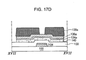
- FIGS. 17A to 17 G are cross sectional views of an exemplary manufacturing method along XVII-XVII of FIG. 16 according to the present invention
- FIGS. 18A to 18 G are cross sectional views of the exemplary manufacturing method along XVIII-XVIII of FIG. 14 according to the present invention
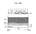
- FIGS. 19A to 19 G are cross sectional views of the exemplary manufacturing method along XIX-XIX of FIG. 15 according to the present invention
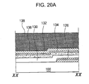
- FIGS. 20A to 20 G are cross sectional views of the exemplary manufacturing method along XX-XX of FIG. 13B according to the present invention.
- a gate line 102 (in FIG. 16), a gate electrode 104 and a gate pad 108 may be formed on a substrate 100 by depositing a first metal layer, and patterning the first metal layer through a first mask process.
- the gate electrode 104 may extend from the gate line 102 , and the gate pad 108 may be located at one end of the gate line 102 .
- First to fourth test pads 110 , 112 114 , and 116 (in FIG. 12), first to fourth connecting lines 120 , 122 , 124 (in FIG. 12), and 126 , a first shorting bar 128 , and a third shorting bar 129 may also be formed on the substrate 100 .
- the first shorting bar 128 may be connected to the odd gate pad 108 a (in FIG. 14) and the third shorting bar 129 may be connected to the odd data pad 150 a (in FIG. 15) to be formed later.
- the first to fourth test pads 110 , 112 , 114 , and 116 may be disposed along one side on the substrate 100 , and may be parallel to the gate line 102 (in FIG. 12).
- the first to fourth connecting lines 120 , 122 , 124 , and 126 may be connected to the first to fourth test pads 110 , 112 , 114 , and 116 , respectively.
- the first shorting bar 128 may be connected to the first connecting line 120
- the third shorting bar 129 may be connected to the third connecting line 124 .
- the first metal layer may include a double layer structure composed of a first layer including aluminum or an aluminum alloy that has relatively low resistance and a second layer including a metal material that can protect the first layer from chemical and thermal degradation, such as chromium (Cr) and molybdenum (Mo).
- a metal material that can protect the first layer from chemical and thermal degradation, such as chromium (Cr) and molybdenum (Mo).
- a gate insulating layer 130 an amorphous silicon layer 132 , a doped amorphous silicon layer 134 , and a second metal layer 136 may be subsequently deposited on the substrate 100 including the gate electrode 104 , the gate pad 108 , the first shorting bar 128 , the third shorting bar 129 , and the fourth connecting line 126 .
- a photoresist layer 138 is formed on the second metal layer 136 by coating photoresist material.
- the gate insulating layer 130 may include an inorganic insulating material, such as silicon nitride (SiNx) and silicon oxide (SiO 2 ), and the second metal layer 136 may include molybdenum.
- a mask 200 having a blocking portion M 11 , a half transmitting portion M 12 , and a transmitting portion M 13 may be disposed over the photoresist layer 138 .
- the half transmitting portion M 12 may correspond to a channel of a thin film transistor, and the blocking portion M 11 may correspond to a data line, source and drain electrodes, a second shorting bar, and a fourth shorting bar to be formed later.
- the photoresist layer 138 may be a positive type, wherein a portion exposed to light is developed and removed.
- the photoresist layer 138 may be exposed to light, and the photoresist layer 138 corresponding to the half transmitting portion M 12 may be exposed to the light by an amount less than the photoresist layer 138 corresponding to the transmitting portion M 13 .
- the photoresist layer 138 (in FIGS. 17B, 18B, 19 B, and 20 B) may be developed, wherein a photoresist pattern having different thicknesses may be formed.
- a first thickness of the photoresist pattern 138 a may correspond to the blocking portion M 11 (in FIGS. 17B, 18B, 19 B, and 20 B), and a second thickness of the photoresist pattern 138 b , which is thinner than the first thickness, may correspond to the half transmitting portion M 12 (in FIG. 17B).
- the second metal layer 136 , the doped amorphous silicon layer 134 , and the amorphous silicon layer 132 (in FIGS.
- a source and drain pattern 136 a a data line 148 (of FIG. 16), a data pad 150 , a second shorting bar 152 , a fourth shorting bar 154 , a doped amorphous silicon pattern 134 a , and an active layer 140 may be formed.
- the second metal layer 136 , the doped amorphous silicon layer 134 , and the amorphous silicon layer 118 may be patterned by a dry etching method since the second metal layer 136 may include molybdenum. Accordingly, fabricating time and costs may be reduced.
- layers including amorphous silicon and doped amorphous silicon may also be formed under the second shorting bar 152 and the fourth shorting bar 154 .
- the layers may have the same shape as the second and fourth shorting bars 152 and 154 .
- the first thickness photoresist pattern 138 b (in FIG. 17C) may be removed through an ashing process, thereby exposing portions of the source and drain pattern 136 a .
- the second thickness photoresist pattern 138 a may also be partially removed and the thickness of the photoresist pattern 138 a may be reduced.
- the source and drain pattern 136 a (in FIG. 17D) and the doped amorphous silicon pattern 134 a (in FIG. 17D) that have been exposed by the photoresist pattern 138 a may be etched, thereby forming source and drain electrodes 142 and 146 and an ohmic contact layer 141 .
- the photoresist pattern 138 a in FIGS. 17D, 18D, 19 D, and 20 D is removed.
- the active layer 140 exposed by the source and drain electrodes 142 and 146 may correspond to the half transmitting portion M 12 (in FIG. 17B).
- the source and drain electrodes 142 and 146 , the data line 148 (in FIG. 16), the ohmic contact layer 141 , and the active layer 140 may be formed through a second mask process using the mask 200 (in FIGS. 17B, 18B, 19 B, and 20 B).
- a passivation layer 156 may be formed on the data line, the source and drain electrodes 142 and 146 , and the second and fourth shorting bars 152 and 154 by coating a transparent organic material, such as benzocyclobutene (BCB) and an acrylic resin, or by depositing an inorganic material, such as silicon nitride (SiNx) and silicon oxide (SiO 2 ).
- a transparent organic material such as benzocyclobutene (BCB) and an acrylic resin
- an inorganic material such as silicon nitride (SiNx) and silicon oxide (SiO 2 ).
- the passivation layer 156 may be patterned through a third mask process, thereby forming a first contact hole 158 , a second contact hole 160 , a third contact hole 162 , a fourth contact hole 164 (in FIG.
- the first contact hole 158 exposes a portion of the drain electrode 146
- the second contact hole 160 exposes a portion of the gate pad 108
- the third contact hole 162 exposes a portion of the data pad 150
- the fourth contact hole 164 (in FIG. 14) exposes a portion of the second shorting bar 152
- the fifth contact hole 166 exposes a portion of the third shorting bar 129
- the sixth contact hole 168 (in FIG.
- the ninth contact hole 174 exposes a portion of the fourth connecting line 126 .
- a pixel electrode 176 may be formed on the passivation layer 156 by depositing a transparent conductive material, such as indium-tin-oxide (ITO) and indium-zinc-oxide (IZO), and patterning the transparent conductive material through a fourth mask process.
- the pixel electrode 176 may be connected to the drain electrode 146 via the first contact hole 158 .
- a gate pad terminal 178 , a data pad terminal 180 , a first conducting pattern 182 (in FIG. 13A), and a second conducting pattern 184 are also formed of the transparent conductive material.
- the gate pad terminal 178 is connected to the gate pad 108 through the second contact hole 160 .
- the gate pad terminal 178 may be connected to the second shorting bar 152 through the fourth contact hole 164 (in FIG. 14).
- the data pad terminal 180 is connected to the data pad 150 and the third shorting bar 129 through the third and fifth contact holes 162 and 166 , respectively.
- the first conducting pattern 182 (in FIG. 13A) is connected to the second shorting bar 152 and the second connecting line 122 through the sixth contact hole 168 and the eighth contact hole 172 , respectively.
- the second conducting pattern 184 is connected to the fourth shorting bar 154 and the fourth connection line 126 through the seventh contact hole 170 and the ninth contact hole 174 , respectively.
- the array substrate of the present invention may be manufactured by using four masks.
- the first to fourth connection lines 120 , 122 , 124 , and 126 , and the first and third shorting bars 128 and 129 may be formed of the same material as the gate electrode material
- the second and fourth shorting bars 152 and 154 may be formed of the same material as the source and drain electrodes material.
- the second and fourth shorting bars 152 and 154 may be connected to the second and fourth connection lines 122 and 126 using the first and second conducting patterns 182 and 184 , respectively.
Abstract
Description
- The present invention claims the benefit of Korean Patent Application No. 2002-20727, filed in Korea on Apr. 16, 2002, which is hereby incorporated by reference.
- 1. Field of the Invention
- The present invention relates to a liquid crystal display (LCD) device and more particularly, to an array substrate for a liquid crystal display device and a manufacturing method thereof.
- 2. Discussion of the Related Art
- Generally, a liquid crystal display (LCD) device includes two substrates that are spaced apart and face each other with a liquid crystal material layer interposed between the two substrates. Each of the substrates includes electrodes that face each other, wherein a voltage applied to each electrode induces an electric field between the electrodes and within the liquid crystal material layer. Alignment of liquid crystal molecules of the liquid crystal material layer is changed by varying an intensity or direction of the applied electric field. Accordingly, the LCD device displays an image by varying light transmissivity through the liquid crystal material layer in accordance with the arrangement of the liquid crystal molecules.
- FIG. 1 is an enlarged perspective view of a liquid crystal display (LCD) device according to the related art. In FIG. 1, an
LCD device 7 has upper andlower substrates crystal material layer 90 interposed between the upper andlower substrates upper substrate 5 includes ablack matrix 2, acolor filter layer 1, and a transparentcommon electrode 18 subsequently disposed on an interior surface thereof. Theblack matrix 2 includes openings having one of three sub-color filters of red (R), green (G), and blue (B). - A
gate line 11 and adata line 36 are formed on an interior surface of thelower substrate 9, which is commonly referred to as an array substrate, such that thegate line 11 and thedate line 36 cross each other to define a pixel area P. In addition, a thin film transistor T is formed at the crossing of thegate line 11 and thedata line 36 and includes a gate electrode, a source electrode, and a drain electrode. Apixel electrode 53 is formed within the pixel area P to correspond to the sub-color filters (R), (G), and (B), and is electrically connected to the thin film transistor T. Thepixel electrode 53 is made of a light transparent conductive material, such as indium-tin-oxide (ITO). - A scanning pulse is supplied to the gate electrode of the thin film transistor T along the
gate line 11, and a data signal is supplied to the source electrode of the thin film transistor T along thedata line 36. Accordingly, light transmission through the liquidcrystal material layer 90 is adjusted by controlling electrical and optical properties of the liquidcrystal material layer 90. For example, the liquidcrystal material layer 90 includes a dielectric anisotropic material having spontaneous polarization properties such that the liquid crystal molecules form a dipole when the electric field is induced. Thus, the liquid crystal molecules of the liquidcrystal material layer 90 are controlled by the applied electric field. In addition, optical modulation of the liquidcrystal material layer 90 is adjusted according to the arrangement of the liquid crystal molecules. Therefore, images of the LCD device are produced by controlling light transmittance of the liquidcrystal material layer 90 due to optical modulation of the liquidcrystal material layer 90. - FIG. 2 is a plan view of an array substrate for an LCD device according to the related art, FIG. 3 is an enlarged plan view of region “A” of FIG. 2 according to the related art, FIG. 4 is an enlarged plan view of region “B” of FIG. 2 according to the related art, and FIG. 5 is an enlarged plan view of region “C” of FIG. 2 according to the related art.
- In FIG. 2,
gate lines 11 anddata lines 36 are formed on asubstrate 9 to cross each other, thereby defining pixel areas P. A thin film transistor T (in FIG. 5) is formed at the crossing of each of the gate anddata lines gate electrode 13 that is connected to thegate line 11 to receive scanning signals, asource electrode 33 is connected to thedata line 36 and receives data signals, and adrain electrode 35 is spaced apart from thesource electrode 33. In addition, the thin film transistor T includes anactive layer 49 between thegate electrode 13 and the source anddrain electrodes transparent pixel electrode 53 is formed in the pixel area P and is connected to thedrain electrode 35. - In FIG. 3, a
gate pad 15 is formed at one end of thegate line 11, and agate pad terminal 60 overlaps thegate pad 15. Thegate pad terminal 60 may be formed of the same material as thepixel electrode 53. Thegate pad 15 includes odd and evengate pads odd gate pad 15 a is connected to afirst shorting bar 17 and the evengate pad 15 b is connected to asecond shorting bar 37. - In FIG. 4, a
data pad 38 is formed at one end of thedata line 36, and adata pad terminal 62 overlaps thedata pad 38. Thedata pad terminal 62 may be formed of the same material as thepixel electrode 53. Thedata pad 38 also includes odd and evendata pads odd data pad 38 a is connected to athird shorting bar 19 and the evendata pad 38 b is connected to afourth shorting bar 39. - In FIGS. 3 and 4, the first to
fourth shorting bars fourth test pads lines fourth test pads substrate 9. The first andthird shorting bars gate line 11, and the second andfourth shorting bars data line 36. Furthermore, the first andthird test pads gate line 11, and the first and third connectinglines data line 36. Accordingly, the evengate pad 15 b is electrically connected to thesecond shorting bar 37 through thegate pad terminal 60, and the evendata pad 38 b is electrically connected to thefourth shorting bar 39 through thedata pad terminal 62. In addition, theshorting bars substrate 9 after the testing process of the array substrate. - FIGS. 6A to 6F are cross sectional views of a manufacturing method of the array substrate using four masks along VI-VI of FIG. 5 according to the related art, and FIGS. 7A to 7F are cross sectional views of a manufacturing method of the array substrate using four masks along VII-VII of FIG. 2 according to the related art.
- In FIGS. 6A and 7A, a
gate electrode 13 is formed on asubstrate 9 by depositing a first metal layer, and patterning the first metal layer through a first mask process. In addition, a gate line 11 (in FIG. 5) and a gate pad 15 (in FIG. 3) are also formed on thesubstrate 9. Next, agate insulating layer 29, anamorphous silicon layer 30, a dopedamorphous silicon layer 31, and asecond metal layer 32 are subsequently deposited on thesubstrate 9 and thegate electrode 13. In addition, aphotoresist layer 70 is formed on thesecond metal layer 32 by coating a photoresist material. Thegate insulating layer 29 is made of an inorganic insulating material, such as silicon nitride (SiNx) and silicon oxide (SiO2), and thesecond metal layer 32 may be formed of chromium (Cr) or molybdenum (Mo). - In FIGS. 6B and 7B, a
mask 80 includes a blocking portion M1, a half transmitting portion M2, and a transmitting portion M3 that are disposed over thephotoresist layer 70, wherein the blocking portion M1 corresponds to a source drain region D and the half transmitting portion M2 corresponds to a channel region E. Thephotoresist layer 70 may be a positive type, wherein a portion exposed to light is developed and removed. Subsequently, thephotoresist layer 70 is exposed to light such that the portion of thephotoresist layer 70 corresponding to the half transmitting portion M2 is exposed to the light in an amount less than thephotoresist layer 70 corresponding to the transmitting portion M3. The half transmitting portion M2 may include slits or semitransparent layer. - In FIGS. 6C and 7C, the exposed photoresist layer 70 (in FIGS. 6B and 7B) is developed, whereby a
photoresist pattern 72 having different thicknesses is formed. A firstthickness photoresist pattern 72 a corresponds to the blocking portion M1 (in FIGS. 6B and 7B) and a second thicknessphotoresist pattern 72 b, which is thinner than thefirst thickness 72 a, corresponds to the half transmitting portion M2 (in FIG. 6B). In addition, there is no photoresist pattern in a region corresponding to the transmitting portion M3 (in FIGS. 6B and 7B). - In FIGS. 6D and 7D, the
second metal layer 32, the dopedamorphous silicon layer 31, and the amorphous silicon layer 30 (of FIGS. 6C and 7C) that have been exposed by thephotoresist pattern 72 are patterned, and thephotoresist pattern 72 is removed. Thus, source anddrain electrodes ohmic contact layer 51, anactive layer 49, and a fourth connecting line 47 (also in FIG. 2) are formed through a second mask process using the mask 80 (in FIGS. 6B and 7B). Accordingly, in FIG. 7D, anamorphous silicon pattern 30 a and a dopedamorphous silicon pattern 31 a are also formed under the fourth connectingline 47. - In FIGS. 6E and 7E, a
passivation layer 56 is formed on the source and drainelectrodes line 47 by coating a transparent organic material, such as benzocyclobutene (BCB) and an acrylic resin, or by depositing an inorganic material, such as silicon nitride (SiNx) and silicon oxide (SiO2). Next, in FIG. 6E, thepassivation layer 56 is patterned through a third mask process, thereby forming adrain contact hole 58 that exposes a portion of thedrain electrode 35. - In FIG. 6F, a
pixel electrode 53 is formed on thepassivation layer 56 by depositing a transparent conductive material, such as indium-tin-oxide (ITO) and indium-zinc-oxide (IZO), and patterning the transparent conductive material through a fourth mask process. Thepixel electrode 53 is connected to thedrain electrode 35 via thedrain contact hole 58. - Alternatively, the second mask process progresses differently depending on a material of the second metal layer 32 (in FIGS. 6C and 7C), such as chromium and molybdenum. The second mask process according to the chromium material will be described hereinafter with reference to figures.
- FIGS. 8A to 8C are cross sectional views of a second mask process of the array substrate along VI-VI of FIG. 5 according to the related art, and FIGS. 9A to 9C are cross sectional views of a second mask process of the array substrate along VII-VII of FIG. 2 according to the related art.
- In FIGS. 8A and 9A, the
second metal layer 32, the dopedamorphous silicon layer 31, and the amorphous silicon layer 30 (in FIGS. 6C and 7C) that have been exposed by the photoresist pattern 72 (in FIGS. 6C and 7C) are removed. The second metal layer 32 (in FIGS. 6C and 7C) that is made of chromium is etched by a wet etching method, and the dopedamorphous silicon layer 31 and the amorphous silicon layer 30 (in FIGS. 6C and 7C) are patterned by a dry etching method. Thus, a source and drainpattern 32 a, a dopedamorphous silicon pattern 51 a, anactive layer 49, and a fourth connectingline 47 are formed. Next, the secondthickness photoresist pattern 72 b (in FIG. 6C) corresponding to the channel region “E” is removed through an ashing process, whereby exposing a portion of the source and drainpattern 32 a. Accordingly, the firstthickness photoresist pattern 72 a is partially removed, thereby reducing the thickness of the firstthickness photoresist pattern 72 a. - In FIGS. 8B and 9B, the source and drain
pattern 32 a (in FIG. 8A) is wet-etched by using the firstthickness photoresist pattern 72 a as an etching mask. Accordingly, in FIG. 8B, source and drainelectrodes amorphous silicon pattern 51 a is exposed. - In FIGS. 8C and 9C, the doped
amorphous silicon pattern 51 a (in FIG. 8B) that is exposed by the source and drainelectrodes ohmic contact layer 51 is formed. In addition, in FIGS. 6D and 7D, the remainingphotoresist pattern 72 a (in FIGS. 8C and 9C) is removed. Thus, if the second metal layer 32 (of FIGS. 6C and 7C) is made of chromium, the second mask process is composed of a first wet-etch step, a first dry-etch step, a second wet-etch step, and a second dry-etch step. Accordingly, total manufacturing time increases. - Alternatively, the second metal layer 32 (in FIGS. 6C and 7C) may be formed of molybdenum, and can be dry-etched. The second mask process according to the molybdenum material will be described hereinafter with reference to figures.
- FIGS. 10A and 10B are cross section views of another second mask process of the array substrate along VI-VI of FIG. 5 according to the related art, and FIGS. 11A and 11B are cross sectional views of another second mask process of the array substrate along VII-VII of FIG. 2 according to the related art.
- In FIGS. 10A and 11A, the
second metal layer 32, the dopedamorphous silicon layer 31, and the amorphous silicon layer 30 (in FIGS. 6C and 7C) that have been exposed by the photoresist pattern 72 (in FIGS. 6C and 7C) are removed by a dry-etching method, wherein thesecond metal layer 32 is made of molybdenum. Thus, a source and drainpattern 32 a, a dopedamorphous silicon pattern 51 a, anactive layer 49, and a fourth connectingline 47 are formed. Next, the secondthickness photoresist pattern 72 b (in FIG. 6C) is removed through an ashing process, whereby exposing a portion of the source and drainpattern 32 a corresponding to the channel region “E.” At this time, the firstthickness photoresist pattern 72 a is partially removed, whereby the thickness of the firstthickness photoresist pattern 72 a is reduced. - In FIGS. 10B and 11B, the source and drain
pattern 32 a (in FIG. 10A) and the dopedamorphous silicon layer 31 a are dry-etched by using the firstthickness photoresist pattern 72 a as an etching mask at a time. Accordingly, source and drainelectrodes ohmic contact layer 51 are formed, and a portion of theactive layer 49 is exposed. As shown in FIGS. 6D and 7D, the remainedphotoresist pattern 72 a (of FIGS. 10B and 11B) is then removed. - However, during the ashing process, the photoresist layer in an outer area on the
substrate 9, that is, thephotoresist pattern 72 a corresponding to the fourth connecting line 47 (in FIG. 11A) is removed at a rate faster than thephotoresist pattern 72 a on the source and drainpattern 32 a (in FIG. 10A). In addition, as shown in FIG. 11B, a part of the fourth connectingline 47 is unintentionally removed. If molybdenum is used as the second metal layer 32 (in FIGS. 6C and 7C), manufacturing time can be reduced, but testing lines, such as shorting bars and connecting lines, may be disconnected. - Accordingly, the present invention is directed to an array substrate for a liquid crystal display device and a manufacturing method thereof that substantially obviates one or more problems due to limitations and disadvantages of the related art.
- An advantage of the present invention is to provide an array substrate for a liquid crystal display device and a manufacturing method thereof that prevents signal disconnection.
- Another object of the present invention is to provide an array substrate for a liquid crystal display device and a manufacturing method thereof that shorten manufacturing time.
- Additional features and advantages of the invention will be set forth in the description which follows, and in part will be apparent from the description, or may be learned by practice of the invention. The objectives and other advantages of the invention will be realized and attained by the structure particularly pointed out in the written description and claims hereof as well as the appended drawings.
- To achieve these and other advantages and in accordance with the purpose of the present invention, as embodied and broadly described, an array substrate for a liquid crystal display device includes a substrate, a plurality of gate lines formed of a first material and a plurality of data lines formed of a second material on the substrate, the plurality of gate lines and the plurality of data lines crossing each other, a plurality of thin film transistors electrically connected to the plurality of gate lines and the plurality of data lines, a plurality of pixel electrodes connected to the plurality of thin film transistors, a plurality of odd-numbered and even-numbered gate pads connected to the plurality of gate lines, a plurality of odd-numbered and even-numbered data pads connected to the plurality of data lines, a first shorting bar electrically connected to each of the odd-numbered gate pads, the first shorting bar made of the first material, a second shorting bar electrically connected to each of the even-numbered gate pads, the second shorting bar made of the second material, a third shorting bar electrically connected to each of the odd-numbered data pads, the third shorting bar made of the first material, a fourth shorting bar electrically connected to each of the even-numbered data pads, the fourth shorting bar made of the second material, first, second, third, and fourth connection lines electrically connected to the first, second, third, and fourth shorting bars, respectively, the first, second, third, and fourth connection lines made of the first material, and first, second, third, and fourth test pads connected to the first, second, third, and fourth connection lines, respectively, the first, second, third, and fourth test pads made of the first material.
- In another aspect, a manufacturing method of an array substrate for a liquid crystal display device includes forming a plurality of gate lines, a plurality of gate electrodes, and a plurality of odd-numbered and even-numbered gate pads on a substrate, forming a gate insulating layer on the plurality of gate lines, the plurality of gate electrodes and the plurality of odd-numbered and even-numbered gate pads, forming a plurality of active layers on the gate insulating layer, forming a plurality of ohmic contact layers on the plurality of active layers, forming a plurality of data lines, a plurality of odd-numbered and even-numbered data pads, a plurality of source electrodes, and a plurality of drain electrodes on the plurality of ohmic contact layers, forming a first shorting bar electrically connected to each of the odd-numbered gate pads, forming a second shorting bar electrically connected to each of the even-numbered gate pads, forming a third shorting bar electrically connected to each of the odd-numbered data pads, forming a fourth shorting bar electrically connected to each of the even-numbered data pads, forming first, second, third, and fourth connection lines electrically connected to the first, second, third, and fourth shorting bars, respectively, forming first, second, third, and fourth test pads connected to the first, second, third, and fourth connection lines, respectively, forming a passivation layer on the plurality of data lines, the plurality of odd-numbered and even-numbered data pads, the plurality of source electrodes, and the plurality of drain electrodes, and forming a plurality of pixel electrodes on the passivation layer, wherein the steps of forming the first shorting bar, the third shorting bar, the first, second, third, and fourth connection lines, and the first, second, third, and fourth test pads are simultaneously performed with the steps of forming the plurality of gate lines, the plurality of gate electrodes, and the plurality of odd-numbered and even-numbered gate pads, and wherein the steps of forming the second shorting bar and the fourth shorting bar are simultaneously performed with the step of forming the plurality of data lines, the plurality of oddnumbered and even-numbered data pads, the plurality of source electrodes, and the plurality of drain electrodes.
- It is to be understood that both the foregoing general description and the following detailed description are exemplary and explanatory and are intended to provide further explanation of the invention as claimed.
- The accompanying drawings, which are included to provide a further understanding of the invention and are incorporated in and constitute a part of this specification, illustrate embodiments of the invention and together with the description serve to explain the principles of the invention. In the drawings:
- FIG. 1 is an enlarged perspective view of a liquid crystal display (LCD) device according to the related art;
- FIG. 2 is a plan view of an array substrate for an LCD device according to the related art;
- FIG. 3 is an enlarged plan view of region “A” of FIG. 2 according to the related art;
- FIG. 4 is an enlarged plan view of region “B” of FIG. 2 according to the related art;
- FIG. 5 is an enlarged plan view of region “C” of FIG. 2 according to the related art;
- FIGS. 6A to 6F are cross sectional views of a manufacturing method of the array substrate using four masks along VI-VI of FIG. 5 according to the related art;
- FIGS. 7A to 7F are cross sectional views of a manufacturing method of the array substrate using four masks along VII-VII of FIG. 2 according to the related art;
- FIGS. 8A to 8C are cross sectional views of a second mask process of the array substrate along VI-VI of FIG. 5 according to the related art;
- FIGS. 9A to 9C are cross sectional views of a second mask process of the array substrate along VII-VII of FIG. 2 according to the related art;
- FIGS. 10A and 10B are cross sectional views of another second mask process of the array substrate along VI-VI of FIG. 5 according to the related art;
- FIGS. 11A and 11B are cross sectional views of another second mask process of the array substrate along VII-VII of FIG. 2 according to the related art;
- FIG. 12 is a plan view of an exemplary array substrate for a liquid crystal display (LCD) device according to the present invention;
- FIG. 13A is an enlarged plan view of region “F” of FIG. 12 according to the present invention;
- FIG. 13B is an enlarged plan view of region “G” of FIG. 12 according to the present invention;
- FIG. 14 is an enlarged plan view of region “H” of FIG. 12 according to the present invention;
- FIG. 15 is an enlarged plan view of region “I” of FIG. 12 according to the present invention;
- FIG. 16 is enlarged plan view of region “J” of FIG. 12 according to the present invention;
- FIGS. 17A to 17G are cross sectional views of an exemplary manufacturing method along XVII-XVII of FIG. 16 according to the present invention;
- FIGS. 18A to 18G are cross sectional views of the exemplary manufacturing method along XVIII-XVIII of FIG. 14 according to the present invention;
- FIGS. 19A to 19G are cross sectional views of the exemplary manufacturing method along XIX-XIX of FIG. 15 according to the present invention; and
- FIGS. 20A to 20G are cross sectional views of the exemplary manufacturing method along XX-XX of FIG. 13B according to the present invention.
- Reference will now be made in detail to the illustrated embodiments of the present invention, which are illustrated in the accompanying drawings.
- FIG. 12 is a plan view of an exemplary array substrate for a liquid crystal display (LCD) device according to the present invention, FIG. 13A is an enlarged plan view of region “F” of FIG. 12 according to the present invention, FIG. 13B is an enlarged plan view of region “G” of FIG. 12 according to the present invention, FIG. 14 is an enlarged plan view of region “H” of FIG. 12 according to the present invention, FIG. 15 is an enlarged plan view of region “I” of FIG. 12 according to the present invention, and FIG. 16 is enlarged plan view of region “J” of FIG. 12 according to the present invention.
- As shown in FIGS. 12-16, a plurality of
gate lines 102 and a plurality ofdata lines 148 may be formed on asubstrate 100 to cross each other, thereby defining pixel areas P. In addition, a thin film transistor T may be formed at the crossing of the gate anddata lines gate electrode 104 connected to thegate line 102 for receiving scanning signals, asource electrode 142 connected to thedata line 148 for receiving data signals, adrain electrode 146 spaced apart from thesource electrode 142, and anactive layer 140 disposed between thegate electrode 104 and the source and drainelectrodes pixel electrode 176 may be formed in the pixel area P, and may be connected to thedrain electrode 146. - In FIG. 14, a
gate pad 108 maybe formed at one end of thegate line 102, and may include odd and evengate pads gate pad terminal 178 may contact and overlap thegate pad 108, and may be formed of the same material as thepixel electrode 176. Theodd gate pad 108 a may be connected to afirst shorting bar 128, and theeven gate pad 108 b may be connected to asecond shorting bar 152 through thegate pad terminal 178. - In FIG. 15, a
data pad 150 may be formed at one end of thedate line 148, and may include odd and evendata pads data pad terminal 180 may contact and overlap thedata pad 150, and may be formed of the same material as thepixel electrode 176. Theodd data pad 150 a may be connected to athird shorting bar 129 through thedata pad terminal 180, and theeven data pad 150 b may be connected to afourth shorting bar 154. - In FIGS. 12, 14 and 15, first to
fourth test pads third shorting bar 129 on thesubstrate 100, and may be spaced apart from each other. The first tofourth test pads lines - In addition, the first and third shorting bars 128 and 129, the first to
fourth test pads lines gate electrode 104, and the second and fourth shorting bars 152 and 154 may be made of the same material as the source and drainelectrodes lines patterns line 126 may not be removed even if the source and drainelectrodes - FIGS. 17A to 17G are cross sectional views of an exemplary manufacturing method along XVII-XVII of FIG. 16 according to the present invention, FIGS. 18A to 18G are cross sectional views of the exemplary manufacturing method along XVIII-XVIII of FIG. 14 according to the present invention, FIGS. 19A to 19G are cross sectional views of the exemplary manufacturing method along XIX-XIX of FIG. 15 according to the present invention, and FIGS. 20A to 20G are cross sectional views of the exemplary manufacturing method along XX-XX of FIG. 13B according to the present invention.
- In FIGS. 17A, 18A, 19A, and 20A, a gate line 102 (in FIG. 16), a
gate electrode 104 and agate pad 108 may be formed on asubstrate 100 by depositing a first metal layer, and patterning the first metal layer through a first mask process. Thegate electrode 104 may extend from thegate line 102, and thegate pad 108 may be located at one end of thegate line 102. - First to
fourth test pads lines first shorting bar 128, and athird shorting bar 129 may also be formed on thesubstrate 100. As detailed above, thefirst shorting bar 128 may be connected to theodd gate pad 108 a (in FIG. 14) and thethird shorting bar 129 may be connected to theodd data pad 150 a (in FIG. 15) to be formed later. The first tofourth test pads substrate 100, and may be parallel to the gate line 102 (in FIG. 12). The first to fourth connectinglines fourth test pads first shorting bar 128 may be connected to the first connectingline 120, and thethird shorting bar 129 may be connected to the third connectingline 124. - Alternatively, the first metal layer may include a double layer structure composed of a first layer including aluminum or an aluminum alloy that has relatively low resistance and a second layer including a metal material that can protect the first layer from chemical and thermal degradation, such as chromium (Cr) and molybdenum (Mo).
- Next, a
gate insulating layer 130, anamorphous silicon layer 132, a dopedamorphous silicon layer 134, and asecond metal layer 136 may be subsequently deposited on thesubstrate 100 including thegate electrode 104, thegate pad 108, thefirst shorting bar 128, thethird shorting bar 129, and the fourth connectingline 126. Aphotoresist layer 138 is formed on thesecond metal layer 136 by coating photoresist material. Thegate insulating layer 130 may include an inorganic insulating material, such as silicon nitride (SiNx) and silicon oxide (SiO2), and thesecond metal layer 136 may include molybdenum. - In FIGS. 17B, 18B, 19B, and 20B, a
mask 200 having a blocking portion M11, a half transmitting portion M12, and a transmitting portion M13 may be disposed over thephotoresist layer 138. The half transmitting portion M12 may correspond to a channel of a thin film transistor, and the blocking portion M11 may correspond to a data line, source and drain electrodes, a second shorting bar, and a fourth shorting bar to be formed later. Thephotoresist layer 138 may be a positive type, wherein a portion exposed to light is developed and removed. Subsequently, thephotoresist layer 138 may be exposed to light, and thephotoresist layer 138 corresponding to the half transmitting portion M12 may be exposed to the light by an amount less than thephotoresist layer 138 corresponding to the transmitting portion M13. - In FIGS. 17C, 18C, 19C, and 20C, the photoresist layer 138 (in FIGS. 17B, 18B, 19B, and 20B) may be developed, wherein a photoresist pattern having different thicknesses may be formed. A first thickness of the
photoresist pattern 138 a may correspond to the blocking portion M11 (in FIGS. 17B, 18B, 19B, and 20B), and a second thickness of thephotoresist pattern 138 b, which is thinner than the first thickness, may correspond to the half transmitting portion M12 (in FIG. 17B). Thesecond metal layer 136, the dopedamorphous silicon layer 134, and the amorphous silicon layer 132 (in FIGS. 17B, 18B, 19B, and 20B) that has been exposed by thephotoresist pattern drain pattern 136 a, a data line 148 (of FIG. 16), adata pad 150, asecond shorting bar 152, afourth shorting bar 154, a dopedamorphous silicon pattern 134 a, and anactive layer 140 may be formed. Then, thesecond metal layer 136, the dopedamorphous silicon layer 134, and the amorphous silicon layer 118 (in FIGS. 17B, 18B, 19B, and 20B) may be patterned by a dry etching method since thesecond metal layer 136 may include molybdenum. Accordingly, fabricating time and costs may be reduced. - In addition, layers including amorphous silicon and doped amorphous silicon may also be formed under the
second shorting bar 152 and thefourth shorting bar 154. The layers may have the same shape as the second and fourth shorting bars 152 and 154. - Next, in FIGS. 17D, 18D, 19D, and 20D, the first
thickness photoresist pattern 138 b (in FIG. 17C) may be removed through an ashing process, thereby exposing portions of the source anddrain pattern 136 a. At this time, the secondthickness photoresist pattern 138 a may also be partially removed and the thickness of thephotoresist pattern 138 a may be reduced. - In FIGS. 17E, 18E, 19E, and 20E, the source and
drain pattern 136 a (in FIG. 17D) and the dopedamorphous silicon pattern 134 a (in FIG. 17D) that have been exposed by thephotoresist pattern 138 a may be etched, thereby forming source and drainelectrodes ohmic contact layer 141. Next, thephotoresist pattern 138 a (in FIGS. 17D, 18D, 19D, and 20D) is removed. Theactive layer 140 exposed by the source and drainelectrodes electrodes ohmic contact layer 141, and theactive layer 140 may be formed through a second mask process using the mask 200 (in FIGS. 17B, 18B, 19B, and 20B). - In FIGS. 17F, 18F, 19F, and 20F, a
passivation layer 156 may be formed on the data line, the source and drainelectrodes passivation layer 156 may be patterned through a third mask process, thereby forming afirst contact hole 158, asecond contact hole 160, athird contact hole 162, a fourth contact hole 164 (in FIG. 14), afifth contact hole 166, a sixth contact hole 168 (in FIG. 13A), aseventh contact hole 170, a eighth contact hole 172 (in FIG. 13A), and aninth contact hole 174. Thefirst contact hole 158 exposes a portion of thedrain electrode 146, thesecond contact hole 160 exposes a portion of thegate pad 108, thethird contact hole 162 exposes a portion of thedata pad 150, the fourth contact hole 164 (in FIG. 14) exposes a portion of thesecond shorting bar 152, thefifth contact hole 166 exposes a portion of thethird shorting bar 129, the sixth contact hole 168 (in FIG. 13A) exposes a portion of thesecond shorting bar 152, theseventh contact hole 170 exposes a portion of thefourth shorting bar 154, the eighth contact hole 172 (in FIG. 13A) exposes a portion of the second connecting line 122 (in FIG. 13A), and theninth contact hole 174 exposes a portion of the fourth connectingline 126. - In FIGS. 17G, 18G, 19G, and 20G, a
pixel electrode 176 may be formed on thepassivation layer 156 by depositing a transparent conductive material, such as indium-tin-oxide (ITO) and indium-zinc-oxide (IZO), and patterning the transparent conductive material through a fourth mask process. Thepixel electrode 176 may be connected to thedrain electrode 146 via thefirst contact hole 158. At this time, agate pad terminal 178, adata pad terminal 180, a first conducting pattern 182 (in FIG. 13A), and asecond conducting pattern 184 are also formed of the transparent conductive material. Thegate pad terminal 178 is connected to thegate pad 108 through thesecond contact hole 160. Thegate pad terminal 178 may be connected to thesecond shorting bar 152 through the fourth contact hole 164 (in FIG. 14). Thedata pad terminal 180 is connected to thedata pad 150 and thethird shorting bar 129 through the third and fifth contact holes 162 and 166, respectively. The first conducting pattern 182 (in FIG. 13A) is connected to thesecond shorting bar 152 and the second connectingline 122 through thesixth contact hole 168 and theeighth contact hole 172, respectively. Thesecond conducting pattern 184 is connected to thefourth shorting bar 154 and thefourth connection line 126 through theseventh contact hole 170 and theninth contact hole 174, respectively. - Accordingly, the array substrate of the present invention may be manufactured by using four masks. In the present invention, the first to
fourth connection lines fourth connection lines second conducting patterns - It will be apparent to those skilled in the art that various modifications and variations can be made in the fabrication and application of the present invention without departing from the spirit or scope of the invention. Thus, it is intended that the present invention cover the modifications and variations of this invention provided they come within the scope of the appended claims and their equivalents.
Claims (21)
Priority Applications (1)
| Application Number | Priority Date | Filing Date | Title |
|---|---|---|---|
| US11/053,438 US7268838B2 (en) | 2002-04-16 | 2005-02-09 | Array substrate for liquid crystal display device and method of manufacturing the same |
Applications Claiming Priority (2)
| Application Number | Priority Date | Filing Date | Title |
|---|---|---|---|
| KR2002-20727 | 2002-04-16 | ||
| KR10-2002-0020727A KR100443539B1 (en) | 2002-04-16 | 2002-04-16 | A array substrate for Liquid crystal display and method for fabricating the same |
Related Child Applications (1)
| Application Number | Title | Priority Date | Filing Date |
|---|---|---|---|
| US11/053,438 Division US7268838B2 (en) | 2002-04-16 | 2005-02-09 | Array substrate for liquid crystal display device and method of manufacturing the same |
Publications (2)
| Publication Number | Publication Date |
|---|---|
| US20030193623A1 true US20030193623A1 (en) | 2003-10-16 |
| US6873392B2 US6873392B2 (en) | 2005-03-29 |
Family
ID=36083942
Family Applications (2)
| Application Number | Title | Priority Date | Filing Date |
|---|---|---|---|
| US10/410,400 Expired - Lifetime US6873392B2 (en) | 2002-04-16 | 2003-04-10 | Array substrate for liquid crystal display device and method of manufacturing the same |
| US11/053,438 Expired - Lifetime US7268838B2 (en) | 2002-04-16 | 2005-02-09 | Array substrate for liquid crystal display device and method of manufacturing the same |
Family Applications After (1)
| Application Number | Title | Priority Date | Filing Date |
|---|---|---|---|
| US11/053,438 Expired - Lifetime US7268838B2 (en) | 2002-04-16 | 2005-02-09 | Array substrate for liquid crystal display device and method of manufacturing the same |
Country Status (8)
| Country | Link |
|---|---|
| US (2) | US6873392B2 (en) |
| JP (1) | JP3672302B2 (en) |
| KR (1) | KR100443539B1 (en) |
| CN (1) | CN100594409C (en) |
| DE (1) | DE10317628B4 (en) |
| FR (1) | FR2838531B1 (en) |
| GB (1) | GB2387708B (en) |
| TW (1) | TWI230306B (en) |
Cited By (3)
| Publication number | Priority date | Publication date | Assignee | Title |
|---|---|---|---|---|
| US20100091212A1 (en) * | 2008-10-10 | 2010-04-15 | Kyo Ho Moon | Array substrate for liquid crystal display device, manufacturing method thereof, and liquid crystal display device having the same |
| US20150199929A1 (en) * | 2014-01-15 | 2015-07-16 | Samsung Display Co., Ltd. | Display panel and display device including the same |
| CN107728393A (en) * | 2017-11-07 | 2018-02-23 | 深圳市华星光电半导体显示技术有限公司 | HVA weld pad sharing structures |
Families Citing this family (26)
| Publication number | Priority date | Publication date | Assignee | Title |
|---|---|---|---|---|
| KR100680701B1 (en) | 2004-07-23 | 2007-02-08 | 엘지전자 주식회사 | Mother Glass and Fabricating Method of Organic Electro Luminescence Device Using The Same |
| KR101051012B1 (en) * | 2004-08-06 | 2011-07-21 | 삼성전자주식회사 | Display panel mother substrate and manufacturing method thereof |
| KR101051008B1 (en) * | 2004-08-24 | 2011-07-21 | 삼성전자주식회사 | Method for producing array substrate and array substrate produced thereby |
| KR101100883B1 (en) * | 2004-11-08 | 2012-01-02 | 삼성전자주식회사 | Thin film transistor array panel |
| KR101107246B1 (en) | 2004-12-24 | 2012-01-25 | 엘지디스플레이 주식회사 | Thin film transistor substrate and fabricating method thereof |
| KR101107245B1 (en) | 2004-12-24 | 2012-01-25 | 엘지디스플레이 주식회사 | Thin film transistor substrate of horizontal electric field and fabricating method thereof |
| KR101080705B1 (en) * | 2004-12-28 | 2011-11-07 | 엘지디스플레이 주식회사 | Chip on glass structure array substrate for Liquid crystal display device |
| KR100663029B1 (en) | 2004-12-31 | 2006-12-28 | 엘지.필립스 엘시디 주식회사 | Liquid crystal display device and method of manufacturing thereof and testing method for thereof |
| US7705924B2 (en) | 2005-02-22 | 2010-04-27 | Samsung Electronics Co., Ltd. | Liquid crystal display and test method thereof |
| TWI271679B (en) * | 2005-05-03 | 2007-01-21 | Chunghwa Picture Tubes Ltd | Array of active devices and method for testing an array of active devices |
| KR101082893B1 (en) * | 2005-08-24 | 2011-11-11 | 삼성전자주식회사 | Array substrate and display apparatus hving the same |
| CN100416344C (en) * | 2006-01-18 | 2008-09-03 | 中华映管股份有限公司 | Base plate of driving part array, liquid crystal display faceplate, and detection method |
| CN100449318C (en) * | 2006-04-11 | 2009-01-07 | 友达光电股份有限公司 | Device and method for detecting whether circuit array is short circuit |
| CN100388108C (en) * | 2006-04-14 | 2008-05-14 | 友达光电股份有限公司 | LCD subassembly and thin film transistor substrate and testing method |
| CN101621038B (en) * | 2008-07-01 | 2011-11-09 | 中华映管股份有限公司 | Manufacturing method of active element array base plate |
| CN101726943B (en) * | 2008-10-21 | 2012-08-22 | 华映视讯(吴江)有限公司 | Active component array substrate, liquid-crystal display panel and detection method for both |
| US9275932B2 (en) | 2011-05-24 | 2016-03-01 | Sharp Kabushiki Kaisha | Active matrix substrate, and display device |
| KR101726641B1 (en) * | 2011-08-03 | 2017-04-26 | 엘지디스플레이 주식회사 | Method of fabricating cliche |
| GB201304939D0 (en) | 2013-03-18 | 2013-05-01 | Cellucomp Ltd | Process for Preparing Cellulose-Containing Particles from Plant Material |
| CN103337477B (en) * | 2013-05-27 | 2015-06-03 | 北京京东方光电科技有限公司 | Fabrication method of array substrate, array substrate and display apparatus |
| CN105182640B (en) * | 2015-09-06 | 2019-06-07 | 京东方科技集团股份有限公司 | Array substrate and display device |
| CN105096899B (en) * | 2015-09-22 | 2018-09-25 | 深圳市华星光电技术有限公司 | Array substrate, liquid crystal display panel and liquid crystal display device |
| CN106444189A (en) * | 2016-10-13 | 2017-02-22 | 京东方科技集团股份有限公司 | Array substrate, detection method thereof and display device |
| US10330996B2 (en) * | 2017-11-07 | 2019-06-25 | Shenzhen China Star Optoelectronics Semiconductor Display Technology Co., Ltd. | Common structure of high vertical alignment pads |
| CN109239999B (en) * | 2018-11-12 | 2020-12-04 | 惠科股份有限公司 | Flexible circuit board, display panel and display device |
| CN112230485B (en) * | 2020-10-27 | 2022-05-20 | 厦门天马微电子有限公司 | Array substrate, display panel and display device |
Citations (8)
| Publication number | Priority date | Publication date | Assignee | Title |
|---|---|---|---|---|
| US5177577A (en) * | 1990-07-05 | 1993-01-05 | Hitachi, Ltd. | Liquid crystal display device with TFT's each including a Ta gate electrode and an anodized Al oxide film |
| US5668032A (en) * | 1995-07-31 | 1997-09-16 | Holmberg; Scott H. | Active matrix ESD protection and testing scheme |
| US6020599A (en) * | 1996-12-04 | 2000-02-01 | Lg Electronics Inc | Liquid crystal display having separable gate lines and gate shorting bar when the connection portion is oxidized |
| US6353464B1 (en) * | 1998-11-20 | 2002-03-05 | Kabushiki Kaisha Advanced Display | TFT array substrate, liquid crystal display using TFT array substrate, and manufacturing method thereof in which the interlayer insulating film covers the guard resistance and the short ring |
| US6380559B1 (en) * | 1999-06-03 | 2002-04-30 | Samsung Electronics Co., Ltd. | Thin film transistor array substrate for a liquid crystal display |
| US6545359B1 (en) * | 1998-12-18 | 2003-04-08 | Semiconductor Energy Laboratory Co., Ltd. | Wiring line and manufacture process thereof, and semiconductor device and manufacturing process thereof |
| US6636279B2 (en) * | 2000-07-24 | 2003-10-21 | International Business Machines Corporation | Display device and method of manufacturing the same |
| US6734925B1 (en) * | 1998-12-07 | 2004-05-11 | Samsung Electronics Co., Ltd. | Multiple testing bars for testing liquid crystal display and method thereof |
Family Cites Families (13)
| Publication number | Priority date | Publication date | Assignee | Title |
|---|---|---|---|---|
| US5486939A (en) * | 1994-04-28 | 1996-01-23 | Xerox Corporation | Thin-film structure with insulating and smoothing layers between crossing conductive lines |
| JP3315834B2 (en) * | 1995-05-31 | 2002-08-19 | 富士通株式会社 | Thin film transistor matrix device and method of manufacturing the same |
| US6613650B1 (en) * | 1995-07-31 | 2003-09-02 | Hyundai Electronics America | Active matrix ESD protection and testing scheme |
| DE69840523D1 (en) * | 1997-01-13 | 2009-03-19 | Hyundai Electronics America | IMPROVED PROTECTION FOR ACTIVE-MATRIX INDICATORS FOR ELECTROSTATIC DISCHARGES AND TESCHEMA |
| KR100244449B1 (en) * | 1997-02-11 | 2000-02-01 | 구본준 | Liquid crystal display having shorting bar for testing thin-film transistor and manufacturing method thereof |
| KR100490040B1 (en) * | 1997-12-05 | 2005-09-06 | 삼성전자주식회사 | Liquid crystal display device with two or more shorting bars and method for manufacturing same |
| KR100281058B1 (en) * | 1997-11-05 | 2001-02-01 | 구본준, 론 위라하디락사 | Liquid Crystal Display |
| KR100569715B1 (en) * | 1998-08-21 | 2006-07-31 | 삼성전자주식회사 | Method of manufacturing flat drive liquid crystal display |
| KR100303207B1 (en) * | 1998-11-13 | 2002-05-13 | 구본준, 론 위라하디락사 | Thin Film Transistor Matrix Substrate with a Testing circuit |
| US6246074B1 (en) * | 1998-09-30 | 2001-06-12 | Lg.Philips Lcd Co., Ltd. | Thin film transistor substrate with testing circuit |
| KR20000026540A (en) * | 1998-10-21 | 2000-05-15 | 윤종용 | Method for manufacturing thin film transistor substrate for lcd using four masks |
| FR2815143B1 (en) * | 2000-10-11 | 2005-11-18 | Lg Philips Lcd Co Ltd | NETWORK SUBSTRATE FOR A LIQUID CRYSTAL DISPLAY AND METHOD OF MANUFACTURING THE SAME |
| KR100769160B1 (en) * | 2000-12-29 | 2007-10-23 | 엘지.필립스 엘시디 주식회사 | Test pad for testing liquid crystal display device |
-
2002
- 2002-04-16 KR KR10-2002-0020727A patent/KR100443539B1/en active IP Right Grant
-
2003
- 2003-04-09 GB GB0308207A patent/GB2387708B/en not_active Expired - Fee Related
- 2003-04-10 US US10/410,400 patent/US6873392B2/en not_active Expired - Lifetime
- 2003-04-14 TW TW092108539A patent/TWI230306B/en not_active IP Right Cessation
- 2003-04-14 JP JP2003109239A patent/JP3672302B2/en not_active Expired - Fee Related
- 2003-04-15 FR FR0304702A patent/FR2838531B1/en not_active Expired - Fee Related
- 2003-04-15 CN CN03109854A patent/CN100594409C/en not_active Expired - Fee Related
- 2003-04-16 DE DE10317628A patent/DE10317628B4/en not_active Expired - Fee Related
-
2005
- 2005-02-09 US US11/053,438 patent/US7268838B2/en not_active Expired - Lifetime
Patent Citations (8)
| Publication number | Priority date | Publication date | Assignee | Title |
|---|---|---|---|---|
| US5177577A (en) * | 1990-07-05 | 1993-01-05 | Hitachi, Ltd. | Liquid crystal display device with TFT's each including a Ta gate electrode and an anodized Al oxide film |
| US5668032A (en) * | 1995-07-31 | 1997-09-16 | Holmberg; Scott H. | Active matrix ESD protection and testing scheme |
| US6020599A (en) * | 1996-12-04 | 2000-02-01 | Lg Electronics Inc | Liquid crystal display having separable gate lines and gate shorting bar when the connection portion is oxidized |
| US6353464B1 (en) * | 1998-11-20 | 2002-03-05 | Kabushiki Kaisha Advanced Display | TFT array substrate, liquid crystal display using TFT array substrate, and manufacturing method thereof in which the interlayer insulating film covers the guard resistance and the short ring |
| US6734925B1 (en) * | 1998-12-07 | 2004-05-11 | Samsung Electronics Co., Ltd. | Multiple testing bars for testing liquid crystal display and method thereof |
| US6545359B1 (en) * | 1998-12-18 | 2003-04-08 | Semiconductor Energy Laboratory Co., Ltd. | Wiring line and manufacture process thereof, and semiconductor device and manufacturing process thereof |
| US6380559B1 (en) * | 1999-06-03 | 2002-04-30 | Samsung Electronics Co., Ltd. | Thin film transistor array substrate for a liquid crystal display |
| US6636279B2 (en) * | 2000-07-24 | 2003-10-21 | International Business Machines Corporation | Display device and method of manufacturing the same |
Cited By (5)
| Publication number | Priority date | Publication date | Assignee | Title |
|---|---|---|---|---|
| US20100091212A1 (en) * | 2008-10-10 | 2010-04-15 | Kyo Ho Moon | Array substrate for liquid crystal display device, manufacturing method thereof, and liquid crystal display device having the same |
| US8879012B2 (en) | 2008-10-10 | 2014-11-04 | Lg Display Co., Ltd. | Array substrate having a shielding pattern, and a liquid crystal display device having the same |
| US20150199929A1 (en) * | 2014-01-15 | 2015-07-16 | Samsung Display Co., Ltd. | Display panel and display device including the same |
| US9691314B2 (en) * | 2014-01-15 | 2017-06-27 | Samsung Display Co., Ltd | Display panel and display device including the same |
| CN107728393A (en) * | 2017-11-07 | 2018-02-23 | 深圳市华星光电半导体显示技术有限公司 | HVA weld pad sharing structures |
Also Published As
| Publication number | Publication date |
|---|---|
| FR2838531B1 (en) | 2004-08-20 |
| TW200305765A (en) | 2003-11-01 |
| JP2003337349A (en) | 2003-11-28 |
| KR100443539B1 (en) | 2004-08-09 |
| CN1453615A (en) | 2003-11-05 |
| CN100594409C (en) | 2010-03-17 |
| GB0308207D0 (en) | 2003-05-14 |
| TWI230306B (en) | 2005-04-01 |
| KR20030082146A (en) | 2003-10-22 |
| GB2387708B (en) | 2004-06-09 |
| DE10317628B4 (en) | 2007-08-09 |
| JP3672302B2 (en) | 2005-07-20 |
| FR2838531A1 (en) | 2003-10-17 |
| GB2387708A (en) | 2003-10-22 |
| US6873392B2 (en) | 2005-03-29 |
| US7268838B2 (en) | 2007-09-11 |
| DE10317628A1 (en) | 2003-10-30 |
| US20050200768A1 (en) | 2005-09-15 |
Similar Documents
| Publication | Publication Date | Title |
|---|---|---|
| US7268838B2 (en) | Array substrate for liquid crystal display device and method of manufacturing the same | |
| US7489369B2 (en) | Array substrate for liquid crystal display device and method of manufacturing the same | |
| US7199846B2 (en) | Method of manufacturing array substrate for liquid crystal display device | |
| US8614780B2 (en) | Array substrate for in-plane switching mode liquid crystal display device having double-layered metal patterns and method of fabricating the same | |
| US6825893B2 (en) | Array substrate for liquid crystal display device having a contact hole situated on active layer and manufacturing method thereof | |
| US8848125B2 (en) | Thin film transistor having a copper signal line | |
| US20020042167A1 (en) | Thin film transistor array substrate for liquid crystal display device and method of manufacturing the same | |
| US8178883B2 (en) | Array substrate for liquid crystal display device and fabricating method of the same | |
| US7301599B2 (en) | Two step maskless exposure of gate and data pads | |
| US7777228B2 (en) | Array substrate for liquid crystal display device and method of fabricating the same | |
| US8198111B2 (en) | Array substrate for liquid crystal display device and method of manufacturing the same | |
| US7847289B2 (en) | Array substrate for liquid crystal display device and method of manufacturing the same | |
| US8243222B2 (en) | Array substrate for liquid crystal display device and method of manufacturing the same |
Legal Events
| Date | Code | Title | Description |
|---|---|---|---|
| AS | Assignment |
Owner name: LG.PHILIPS LCD CO., LTD., KOREA, REPUBLIC OF Free format text: ASSIGNMENT OF ASSIGNORS INTEREST;ASSIGNOR:LIM, BYOUNG-HO;REEL/FRAME:013965/0877 Effective date: 20030409 |
|
| FEPP | Fee payment procedure |
Free format text: PAYOR NUMBER ASSIGNED (ORIGINAL EVENT CODE: ASPN); ENTITY STATUS OF PATENT OWNER: LARGE ENTITY Free format text: PAYER NUMBER DE-ASSIGNED (ORIGINAL EVENT CODE: RMPN); ENTITY STATUS OF PATENT OWNER: LARGE ENTITY |
|
| STCF | Information on status: patent grant |
Free format text: PATENTED CASE |
|
| AS | Assignment |
Owner name: LG DISPLAY CO., LTD., KOREA, REPUBLIC OF Free format text: CHANGE OF NAME;ASSIGNOR:LG.PHILIPS LCD CO., LTD.;REEL/FRAME:021147/0009 Effective date: 20080319 Owner name: LG DISPLAY CO., LTD.,KOREA, REPUBLIC OF Free format text: CHANGE OF NAME;ASSIGNOR:LG.PHILIPS LCD CO., LTD.;REEL/FRAME:021147/0009 Effective date: 20080319 |
|
| FPAY | Fee payment |
Year of fee payment: 4 |
|
| FEPP | Fee payment procedure |
Free format text: PAYOR NUMBER ASSIGNED (ORIGINAL EVENT CODE: ASPN); ENTITY STATUS OF PATENT OWNER: LARGE ENTITY Free format text: PAYER NUMBER DE-ASSIGNED (ORIGINAL EVENT CODE: RMPN); ENTITY STATUS OF PATENT OWNER: LARGE ENTITY |
|
| FPAY | Fee payment |
Year of fee payment: 8 |
|
| FPAY | Fee payment |
Year of fee payment: 12 |