US20030193789A1 - Close packing LED assembly with versatile interconnect architecture - Google Patents
Close packing LED assembly with versatile interconnect architecture Download PDFInfo
- Publication number
- US20030193789A1 US20030193789A1 US10/063,364 US6336402A US2003193789A1 US 20030193789 A1 US20030193789 A1 US 20030193789A1 US 6336402 A US6336402 A US 6336402A US 2003193789 A1 US2003193789 A1 US 2003193789A1
- Authority
- US
- United States
- Prior art keywords
- substrate
- led
- electrical
- edge connector
- set forth
- Prior art date
- Legal status (The legal status is an assumption and is not a legal conclusion. Google has not performed a legal analysis and makes no representation as to the accuracy of the status listed.)
- Granted
Links
Images


Classifications
-
- H—ELECTRICITY
- H01—ELECTRIC ELEMENTS
- H01R—ELECTRICALLY-CONDUCTIVE CONNECTIONS; STRUCTURAL ASSOCIATIONS OF A PLURALITY OF MUTUALLY-INSULATED ELECTRICAL CONNECTING ELEMENTS; COUPLING DEVICES; CURRENT COLLECTORS
- H01R29/00—Coupling parts for selective co-operation with a counterpart in different ways to establish different circuits, e.g. for voltage selection, for series-parallel selection, programmable connectors
-
- F—MECHANICAL ENGINEERING; LIGHTING; HEATING; WEAPONS; BLASTING
- F21—LIGHTING
- F21S—NON-PORTABLE LIGHTING DEVICES; SYSTEMS THEREOF; VEHICLE LIGHTING DEVICES SPECIALLY ADAPTED FOR VEHICLE EXTERIORS
- F21S2/00—Systems of lighting devices, not provided for in main groups F21S4/00 - F21S10/00 or F21S19/00, e.g. of modular construction
- F21S2/005—Systems of lighting devices, not provided for in main groups F21S4/00 - F21S10/00 or F21S19/00, e.g. of modular construction of modular construction
-
- F—MECHANICAL ENGINEERING; LIGHTING; HEATING; WEAPONS; BLASTING
- F21—LIGHTING
- F21S—NON-PORTABLE LIGHTING DEVICES; SYSTEMS THEREOF; VEHICLE LIGHTING DEVICES SPECIALLY ADAPTED FOR VEHICLE EXTERIORS
- F21S4/00—Lighting devices or systems using a string or strip of light sources
- F21S4/10—Lighting devices or systems using a string or strip of light sources with light sources attached to loose electric cables, e.g. Christmas tree lights
-
- F—MECHANICAL ENGINEERING; LIGHTING; HEATING; WEAPONS; BLASTING
- F21—LIGHTING
- F21V—FUNCTIONAL FEATURES OR DETAILS OF LIGHTING DEVICES OR SYSTEMS THEREOF; STRUCTURAL COMBINATIONS OF LIGHTING DEVICES WITH OTHER ARTICLES, NOT OTHERWISE PROVIDED FOR
- F21V23/00—Arrangement of electric circuit elements in or on lighting devices
- F21V23/06—Arrangement of electric circuit elements in or on lighting devices the elements being coupling devices, e.g. connectors
-
- F—MECHANICAL ENGINEERING; LIGHTING; HEATING; WEAPONS; BLASTING
- F21—LIGHTING
- F21Y—INDEXING SCHEME ASSOCIATED WITH SUBCLASSES F21K, F21L, F21S and F21V, RELATING TO THE FORM OR THE KIND OF THE LIGHT SOURCES OR OF THE COLOUR OF THE LIGHT EMITTED
- F21Y2113/00—Combination of light sources
- F21Y2113/10—Combination of light sources of different colours
- F21Y2113/13—Combination of light sources of different colours comprising an assembly of point-like light sources
-
- F—MECHANICAL ENGINEERING; LIGHTING; HEATING; WEAPONS; BLASTING
- F21—LIGHTING
- F21Y—INDEXING SCHEME ASSOCIATED WITH SUBCLASSES F21K, F21L, F21S and F21V, RELATING TO THE FORM OR THE KIND OF THE LIGHT SOURCES OR OF THE COLOUR OF THE LIGHT EMITTED
- F21Y2115/00—Light-generating elements of semiconductor light sources
- F21Y2115/10—Light-emitting diodes [LED]
-
- H—ELECTRICITY
- H01—ELECTRIC ELEMENTS
- H01R—ELECTRICALLY-CONDUCTIVE CONNECTIONS; STRUCTURAL ASSOCIATIONS OF A PLURALITY OF MUTUALLY-INSULATED ELECTRICAL CONNECTING ELEMENTS; COUPLING DEVICES; CURRENT COLLECTORS
- H01R12/00—Structural associations of a plurality of mutually-insulated electrical connecting elements, specially adapted for printed circuits, e.g. printed circuit boards [PCB], flat or ribbon cables, or like generally planar structures, e.g. terminal strips, terminal blocks; Coupling devices specially adapted for printed circuits, flat or ribbon cables, or like generally planar structures; Terminals specially adapted for contact with, or insertion into, printed circuits, flat or ribbon cables, or like generally planar structures
- H01R12/50—Fixed connections
- H01R12/51—Fixed connections for rigid printed circuits or like structures
- H01R12/52—Fixed connections for rigid printed circuits or like structures connecting to other rigid printed circuits or like structures
-
- H—ELECTRICITY
- H05—ELECTRIC TECHNIQUES NOT OTHERWISE PROVIDED FOR
- H05K—PRINTED CIRCUITS; CASINGS OR CONSTRUCTIONAL DETAILS OF ELECTRIC APPARATUS; MANUFACTURE OF ASSEMBLAGES OF ELECTRICAL COMPONENTS
- H05K1/00—Printed circuits
- H05K1/02—Details
- H05K1/14—Structural association of two or more printed circuits
- H05K1/142—Arrangements of planar printed circuit boards in the same plane, e.g. auxiliary printed circuit insert mounted in a main printed circuit
-
- Y—GENERAL TAGGING OF NEW TECHNOLOGICAL DEVELOPMENTS; GENERAL TAGGING OF CROSS-SECTIONAL TECHNOLOGIES SPANNING OVER SEVERAL SECTIONS OF THE IPC; TECHNICAL SUBJECTS COVERED BY FORMER USPC CROSS-REFERENCE ART COLLECTIONS [XRACs] AND DIGESTS
- Y10—TECHNICAL SUBJECTS COVERED BY FORMER USPC
- Y10S—TECHNICAL SUBJECTS COVERED BY FORMER USPC CROSS-REFERENCE ART COLLECTIONS [XRACs] AND DIGESTS
- Y10S362/00—Illumination
- Y10S362/80—Light emitting diode
Abstract
A modular mounting assembly (10) for connecting a plurality of LED's in a selectable electrical and spatial arrangement includes a plurality of substrates (12) each having at least one LED (14 a, 14 b) fixedly arranged thereon, and a plurality of connectors (16) arranged thereon that are in operative communication with the at least one LED (14 a, 14 b) fixedly arranged thereon. The plurality of substrates (12) are arranged in a selected spatial arrangement having selected pairs of connectors (16) in operative communication with each other to effectuate electrical connection therebetween, whereby an electrical arrangement of the plurality of LED's is effectuated. A plurality of interconnecting elements (50A, 50D, 50S, 50P) electrically and structurally interconnect selected spatially adjacent substrates (12) in cooperation with the selected pairs of connectors. A connector (16) has a plurality of electrical conductor members (1, 2, 3, 4, 5), and an interconnecting element (50) has a selected electrical configuration that effectuates a selected interconnection of conductor members (1, 2, 3, 4, 5).
Description
- The invention relates to the electronic and optoelectronic arts. It is especially applicable to the packaging of light emitting diodes (LED's), and will be described with particular reference thereto. However, the invention will also find application in the packaging other electronic and optoelectronic devices, such as photodetectors, signal receivers, vertical cavity surface emitting lasers (VCSEL's), photovoltaic devices, and the like.
- Light emitting diodes (LED's) find application in fiber optical communications, lighting applications, display applications, and other applications where a compact, low voltage, rugged, and high efficiency light source is advantageous. In many LED applications, a plurality of LED's are advantageously arranged into an array or other pre-determined arrangement comprising similar or dissimilar LED types. In lighting or display applications, LED's emitting in the red, green, and blue regions are preferably closely packed to form a color “pixel” that blends the three colors. In this manner white light can be generated. Alternatively, by selectively varying the optical output intensity of the three colored LED's, a selected color can be generated. An array of such “pixels” can form a color display or an illuminating surface emitting white light, among other applications.
- The prior art includes fabrication of LED arrays on-chip. In this approach, semiconductor layers comprising the LED's are generated on a substrate, usually a semiconductor substrate, and individual LED's of the array are isolated by etching mesas in the LED layers. This approach is limited in application. The LED's are typically required to be all of one type. The choice of substrate is limited to those compatible with the semiconductor layer generation method. Many commercial LED's are formed from III-V compound semiconductor layers, and the substrates which are used for the growth of such layers, typically including GaAs and InP wafers, sapphire substrates, and the like, are often expensive, fragile, and of limited lateral area.
- A much more flexible approach is to fabricate discrete LED's using any convenient method, and then to bond the discrete LED's to a host substrate to form the LED arrangement thereon. In this manner dissimilar LED's, such as red, green, and blue LED's comprised of different material layers, can be advantageously combined. The choice of substrate is greatly expanded. However, the individual LED's are electrically isolated, so that intricate wire bonding or other electrical interconnecting methods are typically applied to complete the array. Additionally, a different host substrate shape and electrical interconnect pattern is needed for each distinct LED arrangement, which limits the standardization of parts and complicates array manufacturing.
- The present invention contemplates an improved modular mounting assembly for forming arrays of LED's and other components.
- In accordance with one embodiment of the present invention, a mounting structure for assembling a plurality of optoelectronic components is disclosed. A first substrate has at least one first optoelectronic component arranged thereon. The first substrate is in the shape of a rhombus and has an edge connector disposed on an edge thereof. A second substrate has at least one second optoelectronic component arranged thereon. The second substrate is in the shape of a rhombus and has an edge connector disposed on an edge thereof which operatively connects with the edge connector of the first substrate to form an arrangement of the at least one first optoelectronic component and the at least one second optoelectronic component.
- In accordance with another aspect of the present invention, at least one of the first substrate and the second substrate has a rhombus shape that corresponds to a primitive unit cell of a hexagon.
- In accordance with another aspect of the present invention, an interconnecting element connects with the edge connector of the first substrate and with the edge connector of the second substrate to connect the edge connector of the first substrate with the edge connector of the second element.
- In accordance with another aspect of the present invention, the first substrate includes an electrical connection between the at least one first component and the edge connector of the first substrate. The second substrate includes an electrical connection between the at least one second component and the edge connector of the second substrate. The interconnecting element electrically connects the edge connector of the first substrate with the edge connector of the second substrate to form an electrical arrangement of the at least one first component and the at least one second component.
- In accordance with another aspect of the present invention, the first substrate includes a thermally conductive layer, and a printed circuit board into which the edge connector is formed. The printed circuit board includes an electrical path connecting the at least one first optoelectronic component with the edge connector.
- In accordance with another aspect of the present invention, the at least one first optoelectronic component includes at least one light emitting diode (LED). The first substrate includes a lens in operative communication with the at least one LED.
- In accordance with another aspect of the present invention, the at least one first optoelectronic component includes a plurality of light emitting diodes (LED's) disposed on the substrate. The printed circuit board includes an electrical path that electrically interconnects the LED's disposed on the substrate.
- In accordance with another aspect of the present invention, the thermally conductive layer has depressions in which the LED's are arranged, and the printed circuit board has holes arranged to allow the LED light emission to pass through.
- In accordance with another aspect of the present invention, a third substrate has at least one third component arranged thereon. The third substrate is in the shape of a rhombus and has a first edge connector disposed on an edge thereof which operatively connects with a second edge connector of the first substrate. The third substrate also has a second edge connector disposed on an edge thereof which operatively connects with a second edge connector of the second substrate. The first, second, and third rhombus-shaped substrates are arranged to form a hexagonally shaped mounting structure.
- In accordance with another aspect of the present invention, at least one terminating element completes an electrical circuit.
- In accordance with another aspect of the present invention, at least one terminating element supplies electrical power to the mounting structure.
- In accordance with another embodiment of the present invention, a modular mounting assembly for connecting a plurality of light emitting diodes (LED's) in a selectable electrical and spatial arrangement is disclosed. A plurality of substrates are provided. Each substrate has at least one LED fixedly arranged thereon, and a plurality of connectors arranged thereon that are in electrical communication with the at least one LED. The plurality of substrates are arranged in a spatial arrangement having selected pairs of connectors in electrical communication with each other providing an electrical arrangement between the plurality of LED's.
- In accordance with another aspect of the present invention, an interconnecting element electrically and structurally interconnects selected substrates through pairs of connectors. For example, an interconnecting element cooperates with the selected substrates to form one of a series LED electrical interconnection and a parallel LED electrical interconnection.
- In accordance with another aspect of the present invention, at least one of the plurality of substrates has a rhombic shape.
- In accordance with yet another embodiment of the present invention, an extensible LED structure is disclosed. An LED is supported by a rhomboidal shaped substrate. At least one electrical socket is disposed on the rhomboidal shaped substrate and shaped to receive an electrical plug. The electrical socket provides electrical communication to the LED.
- In accordance with another aspect of the present invention, a discrete plug mechanically connects the electrical socket to an electrical socket disposed on a second substrate.
- In accordance with another aspect of the present invention, a plug is integral with the substrate. The plug is mechanically connectable to an electrical socket disposed on a second substrate.
- In accordance with another aspect of the present invention, the plug comprises electrical paths and when the plug is seated in the socket, the electrical paths place the LED in a predetermined electrical relationship with an LED on the second substrate.
- The advantages and benefits of the present invention will become apparent to those of ordinary skill in the art upon reading and understanding the following detailed description.
- The invention may take form in various components and arrangements of components, and in various steps and arrangements of steps. The drawings are only for purposes of illustrating a preferred embodiment and are not to be construed as limiting the invention.
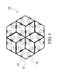
- FIG. 1 shows an exemplary array of twelve rhombic substrates forming a hexagonal array of twenty-four components.
- FIG. 2 shows the geometry of an exemplary rhombic substrate.
- FIG. 3 shows a first embodiment of the invention, having two LED components connected electrically in series on a rhombic substrate.
- FIG. 4 shows a sectional view of the embodiment of FIG. 3 taken along the Section S-S.
- FIG. 5 shows an electrical schematic of the substrate of FIG. 3.
- FIG. 6 shows an exemplary interconnecting element that is compatible with the substrate of FIGS. 3 and 5.
- FIG. 7 shows an exploded view of an exemplary interconnection of three rhombic substrates corresponding to the embodiment of FIGS. 3 and 5.
- FIG. 8A shows an electrical schematic of a series connection of two substrates corresponding to the substrate embodiment of FIGS. 3 and 5.
- FIG. 8B shows an exemplary interconnecting element that implements the series interconnection shown in FIG. 8A
- FIG. 9A shows an electrical schematic of a parallel connection of two substrates corresponding to the substrate embodiment of FIGS. 3 and 5.
- FIG. 9B shows an exemplary interconnecting element that implements the parallel interconnection shown in FIG. 8A.
- FIG. 10A shows an electrical schematic of a terminating element that connects the cathode of the last substrate according to the substrate embodiment of FIGS. 3 and 5 to circuit ground.
- FIG. 10B shows an exemplary interconnecting element that implements the circuit termination shown in FIG. 10A.
- FIG. 11A shows an electrical schematic of a terminating element that connects a substrate of the type shown in FIGS. 3 and 5 to a voltage source.
- FIG. 11B shows an exemplary interconnecting element that implements the voltage connection shown in FIG. 11A.
- FIG. 12 shows an exemplary series interconnection of three substrates of the type shown in FIGS. 3 and 5 using appropriate interconnecting and terminating elements.
- FIG. 13 shows a second embodiment of the invention, having two sets of red, green, and blue LED components that provides independent electrical access to the three colors.
- FIG. 14 shows an electrical schematic of the substrate of FIG. 13.
- FIG. 15 shows a third embodiment of the invention that includes a connector appropriate for connection to a connecting cable.
- FIG. 16 shows an exemplary arrangement of several substrates of the type shown in FIG. 15 on an interconnecting cable.
- With reference to FIGS. 1 and 2, a modular mounting
assembly 10 is described. A plurality ofsubstrates 12 each have one ormore components 14 arranged thereon. In the illustrated embodiment of FIG. 7, eachsubstrate 12 has two LEDcomponents 14 arranged thereon. The plurality ofsubstrates 12 are arranged in a selected manner to form the mountingassembly 10 that arranges thecomponents 14 in a selected arrangement, such as the hexagonal arrangement of FIG. 1 comprised of twelvesubstrates 12 and twenty fourLED components 14. - In one embodiment shown in FIGS. 1 and 2, each
substrate 12 has the shape of a rhombus, i.e. a parallelogram having four sides of essentially equal length L, with oppositely oriented angles equal. Thus, a rhombus can be specified by two angular parameters α and β, along with the side length L, as shown in FIG. 2. In the illustrated embodiment of FIG. 1, the angles α and β are 60° and 120°, respectively, so that eachrhombic substrate 12 corresponds to a primitive unit cell of a hexagon, thus enabling particularly close packing of thecomponents 14 such as in theassembly 10 shown in FIG. 1. Hexagonal symmetry is particularly advantageous because hexagons can be arranged to form densely packed two-dimensional arrays. Hexagonal symmetry also can be used to create three-dimensional structures such as spheres or geodesic-type domes. - In another embodiment (not shown), α=β=90° so that a square unit cell substrate results. It will be appreciated that the rhombic shape provides a high degree of symmetry that enables arrangement of a plurality of
rhombic substrates 12 into a wide range of selected spatial arrangements. Of course, other values for the angles α and β can also be used within the geometrical limitation that α+β=180° for the rhombic geometry shown in FIG. 2. - With continuing reference to FIG. 1, each
substrate 12 includes one ormore connectors 16 that effectuate interconnection of thesubstrates 12. In one embodiment, theconnectors 16 also cooperate to effectuate electrical interconnection of thecomponents 14 across the boundaries of pairedsubstrates 12. - With reference now to FIGS. 3 and 4, the
substrate 12 is described. Eachsubstrate 12 has two LEDcomponents - With particular reference now to FIG. 4, which shows a sectional view taken along the Section S-S shown in FIG. 3, the
substrate 12 includes a thermallyconductive layer 20, such as a copper plate. In an exemplary embodiment a copper plate about 0.3 cm thick is used. Each LED component arranged on thesubstrate 12, e.g. theexemplary LED 14 a is disposed in a receivingdepression 22 of thecopper plate 20. The receivingdepression 22 is a conical well with a flat bottom. The mounting of an LED die therein can employ thermally conductive cement, a resin, an epoxy, or the like, as is well known to those of ordinary skill in the art. The thermallyconductive layer 20 provides heat sinking for theLED components LED components copper plate 20. - An insulating layer such as a printed circuit board (PC board) 24 is affixed to the thermally
conductive layer 20. ThePC board 24 has one or more openings orholes 26 corresponding to the receivingwells 22 of thecopper plate 20, through which the LED light emission passes during LED operation. Thesubstrate 12 optionally includes additional optical components, such as atransparent cover plate 30 and alens 32 that is in operative communication with theLED 14 a. - With continuing reference to FIGS. 3 and 4, the
PC board 24 advantageously facilitates electrical connections to the components. A plurality of PC board traces connect the LED's 14 a, 14 b to theconnectors 16 and optionally also connect the LED's 14 a, 14 b to each another. For example, atrace 40 can be used to interconnect the LED's 14 a, 14 b electrically in series. The electrodes (not shown) of theLED components 14 are connected to the PC board traces 40 using wire bonds or other means (not shown) that are well known to those of ordinary skill in the art. In one embodiment, theconnectors 16 are formed into the edges of thePC board 24 so that the traces advantageously directly connect to the electrical conductor members comprising theconnectors 16, and theconnectors 16 are readily accessible at the edges of thesubstrate 12. In the illustrated exemplary embodiment of FIG. 3, there are fourconnectors 16, and each connector has fiveconductor members - With reference now to FIG. 5, an electrical circuit schematic is shown corresponding to the
exemplary substrate 12 of FIGS. 3 and 4. In the illustrated exemplary embodiment of FIG. 5, the LED's 14 a, 14 b are connected in series on thesubstrate 12. Theanode 44 and thecathode 46 of theseries LED combination connector conductor members exemplary substrate 12, it will be appreciated that providing additional conductor members, e.g.unattached members substrate 12 and enhances the modularity of the system. Additionally, at least one conductor member is reserved as a circuit ground. In the exemplary embodiment of FIGS. 3 and 5,conductor member 4 is reserved as the ground conductor. Of course, it will also be recognized that other conductor designations can be made, and additionally more or fewer than five conductor members can be included on eachconnector 16. However, for a given modular mounting assembly some standardization of the number and designations of the conductors is highly advantageous. - With reference now to FIGS. 6 and 7, an approach for effectuating the interconnection of pairs of
connectors 16 is described. An interconnectingelement 50A of a type “A” operatively connects to a pair ofconnectors 16 atmating ports element 50A. The interconnectingelement 50A mechanically connects to the twosubstrates 12 that have the pair ofconnectors 16 to effectuate structural interconnection between the twosubstrates 12. The mechanical connection can be by a frictional fit (not shown) or byfastenings 56 which can be screws, rivets, or the like. The interconnectingelement 50A also has a pre-selected electrical configuration that effectuates a desired electrical arrangement of the components of theconnected substrates 12, such as a series connection arrangement, parallel connection arrangement, or the like. As can be seen in FIG. 6, the twomating ports electrical connector members 1′, 2′, 3′, 4′, 5′ that correspond to and electrically connect with theconnector members connectors 16 of thesubstrates 12. The pre-selected electrical configuration is determined by the electrical interconnections of the twoports element 50A (not shown in FIG. 6). Thus, as shown in FIG. 7, two interconnectingelements 50A of type “A” that has a particular electrical configuration are used in conjunction with athird interconnecting element 50D of type “D” that has a different electrical configuration, to generate a selected electrical arrangement of the components on the threesubstrates 12. Those skilled in the art will appreciate that other shaped interconnecting elements can be substituted with no loss of functionality. Also, the interconnecting element or plug does not necessarily have to be separate from the substrates. That is, integral plugs can be formed on, for example, opposing sides of the substrate and configured to closely fit with the connectors or sockets of adjacent substrates. - Because the interconnecting
element 50A in one embodiment is structurally symmetric but not necessarily electrically symmetric, the interconnectingelement 50A includes an orientation key 58 that indicates the electrical orientation. The interconnectingelement 50A also has an identifying mark “A” 60 indicating that it is a type “A” interconnectingelement 50A. Of course, other marks, a color coding scheme, or the like can also be used to identify the interconnecting element type. For example, a colored band (not shown) can be asymmetrically placed on the interconnectingelement 50A, in which the color correlates with the interconnecting element type and the asymmetric placement provides an orientation key. - With reference now to FIGS. 8A through 11B, four exemplary electrical configurations for interconnecting and terminating elements are described. The exemplary electrical configurations are described with reference to the electrical configuration of the substrate shown in FIGS. 3 and 5 in which each
substrate 12 has two series-connectedLED components conductor element 4 as the circuit ground. - With particular reference now to FIGS. 8A and 8B, a series interconnection of two
such substrates 12 is described. The pre-selected series electrical configuration is shown in FIG. 8A. An interconnectingelement 50S electrically connects theconductor member 5 of afirst substrate 12 with theconductor member 7 of asecond substrate 12 to effectuate a series interconnect. Additionally, theground conductor members 4 are connected to provide ground continuity across thesubstrates 12. As shown in FIG. 8B, this corresponds to the illustratedinterconnecting element 50S in which theconductor member 5′ of thefirst port 52S is electrically connected with theconductor member 1′ of thesecond port 54S to effectuate the series interconnection, and theconductor member 4′ of thefirst port 52S is electrically connected with theconductor member 4′ of thesecond port 54S to maintain ground continuity. - With particular reference now to FIGS. 9A and 9B, a parallel interconnection of two
substrates 12 is described. The pre-selected parallel electrical configuration is shown in FIG. 9A. An interconnectingelement 50P electrically connects theconductor member 1 of afirst substrate 12 with theconductor member 1 of asecond substrate 12, and interconnects theconductor member 5 of thefirst substrate 12 with theconductor member 5 of thesecond substrate 12, to effectuate the parallel interconnect. Additionally, theconductor member 4 of thefirst substrate 12 is interconnected with theconductor member 4 of thesecond substrate 12 to effectuate ground continuity across the substrates. As shown in FIG. 9B, this corresponds to the illustratedinterconnecting element 50P in which theconductor member 7′ of thefirst port 52P is electrically connected with theconductor member 7′ of thesecond port 54P, theconductor member 5′ of thefirst port 52P is electrically connected with theconductor member 5′ of thesecond port 54P, and theconductor member 4′ of thefirst port 52P is electrically connected with theconductor member 4′ of thesecond port 54P. - With particular reference now to FIGS. 10A and 10B, a terminating
element 50T is shown. The terminatingelement 50T is appropriate, for example, for terminating one or more series- or parallel-interconnected substrates 12. An electrical schematic showing the operation of the terminatingelement 50T is shown in FIG. 10A. The terminatingelement 50T electrically connects theconductor member 5 of thelast substrate 12 to the circuitground conductor member 4. As shown in FIG. 10B, this corresponds to the illustrated terminatingelement 50T which has only asingle port 52T that has itsconductor member 5′ electrically connected with theconductor member 4′ to effectuate the grounding of theconductor member 5′. - With particular reference now to FIGS. 11A and 11B, a terminating
element 50V providing electrical power to a circuit assembly is described. The terminatingelement 50V is appropriate, for example, for connecting one or more series- or parallel-interconnected substrates 12 to a source of electrical power. The electrical configuration is shown in FIG. 11A. The terminatingelement 50V electrically connects theconductor member 1 to the positive terminal of an associated voltage source V, and also connects theground conductor member 4 to the negative terminal of the associated voltage source V. As shown in FIG. 11B, this corresponds to the illustrated terminatingelement 50V which has only asingle port 54V. Theconductor member 1′ is electrically connected with the positive terminal of the associated voltage source V, while theconductor member 4′ is electrically connected to the negative terminal of the associated voltage source V. In one embodiment, the terminatingelement 50V connects to the associated voltage source V through anelectrical cable 64 that is disposed between the terminatingelement 50V and the voltage source V. Of course, other electrical connecting and transmission elements can also be included, such as a jack (not shown) that detachably connects thecable 64 to the terminatingelement 50V, and/or a jack (not shown) that detachably connects thecable 64 to the voltage supply V. - Other interconnecting and terminating elements are also contemplated. For example, a “null” interconnecting element (not shown) having no electrical interconnections therein can be provided. Such a “null” connecting element advantageously provides structural support to the modular mounting assembly without including corresponding electrical interconnections. It will also be recognized that the specific electrical configurations of the interconnecting elements depend upon both the selected electrical interconnection and on the electrical configuration of the substrate. The exemplary interconnecting and terminating elements of FIGS. 5A through 11B are appropriate for the
substrate 12 illustrated in FIGS. 3 and 5. Regardless of the electrical configuration, the mechanical configuration of the interconnecting elements is advantageously standardized to facilitate formation of complex modular mounting structures such as thehexagonal structure 10 of FIG. 1. - In one aspect of the invention, standardized substrates are provided on which components, such as LED components, can be affixed. These substrates in combination with standardized interconnecting and terminating elements together cooperate to form selected modular interconnections of LED components. The interconnecting and terminating elements can advantageously include orientation
key marks 58 andtype indicators 60 to avoid misconnection. Although symbolic type indicators are shown in exemplary FIGS. 6 and 7, other type indicators such as color coding schemes are also contemplated. Theports - With reference now to FIG. 12, an exemplary assembly of six LED components on three
substrates 12 is shown. Power is supplied from the voltage source V via a terminatingelement 50V. The threesubstrates 12 are interconnected using twoseries interconnecting elements 50S. The series string is terminated by a terminatingelement 50T, which differs from the terminatingelement 50T of FIGS. 10A and 10B in that an electrically unconnected second port is included to provide improved structural integrity. Although the extra port of terminatingelement 50T′ is shown as completely electrically unconnected, in another contemplated embodiment theground terminals 4′ of the two ports are interconnected to provide additional ground continuity. In yet another contemplated embodiment (not shown) the terminatingelement 50T′ is replaced by a completely electrically unconnected interconnecting element that has no electrical interconnections and provides only structural support to the modular mounting, and a connector oftype 50T is connected to one of the unpaired ports of thelast substrate 12 in the electrical series to provide the electrical termination. - The illustrated modular configuration of FIG. 12 can be converted to a configuration having the three
substrates 12 in parallel with the twoLED components substrate 12 connected in series by simply replacing the twoseries interconnecting elements 50S with correspondingparallel interconnecting elements 50P. The exemplary circuit shown in FIG. 12 is rather simple. However, it will be appreciated that highly complex modular assemblies including dozens, hundreds, or even greater numbers of LED components having complex spatial arrangements, electrical interconnections, electrical sub-circuits, and the like can be created by appropriate selection and arrangement of a standardized set of substrates, interconnecting elements, and terminating elements. Another advantage of the present invention is that replacement of a failed LED component is greatly simplified, and requires only replacement of the substrate on which the failed LED component is disposed. - With reference now to FIGS. 13 and 14, another embodiment of the modular mounting assembly is described. A substrate 12RGB has six LED components arranged thereon: a first
red LED component 14 aR, a firstgreen LED component 14 aG, and a firstblue LED component 14 aB arranged in a first receiving well 22 a; and a secondred LED component 14 bR, a secondgreen LED component 14 bG, and a secondblue LED component 14 barranged in a second receiving well 22 b, as shown. The first and second LED component of each color is connected in series by PC board traces 40R, 40G, and 40G. In order to accommodate the greater number of anode and cathode terminals in this tri-color substrate 12RGB, connectors 16RGB having seven conductor members each is used. As shown in the electrical schematic of FIG. 14, each of the three colors is independently addressable:conductor members conductor members conductor members conductor member 1 serves as circuit ground in the substrate 12RGB. For substrates having more complex interconnections such as those shown in FIGS. 13 and 14, two-level or even more complex PC boards can be used to accommodate the larger number of traces involved. - It will be appreciated by those of ordinary skill in the art that the substrates comprising a modular mounting assembly need not have identical components arranged thereon, as long as the connectors are electrically and structurally compatible. Thus, for example, substrates having low intensity LED components (not shown) and substrates having high intensity LED components (not shown) can be intermixed in an array to form a dual-intensity lamp. Because the electrical characteristics of LED components of different intensities often differ, and because it can be desirable to independently address the low intensity LED and the high intensity LED sub-arrays, different electrical conductor members can be advantageously used for the different LED intensities. Thus, for example, in a five-conductor connector,
conductors conductors conductor 5 can be used as the system ground. The substrates having only high intensity LED components advantageously have theconductor members 1 of the various connectors interconnected on the substrate, and similarly theconductor members 2 of the various connectors are advantageously interconnected, whereby electrical continuity for the low intensity sub-circuit is provided across the modular assembly. Similarly, the highintensity conductor members - In another contemplated variation, blank substrates, e.g. substrates having no components thereon, can advantageously be used as spaceholders in the modular assembly. Once again, like electrical conductor members of the blank substrate connectors can be interconnected on the substrate to provide electrical continuity where necessary.
- With reference now to FIGS. 15 and 16, yet another embodiment of the invention is described, that is particularly suitable for interconnecting LED components on a flexible cable or other linear element. Such “LED strings” can be used as flexible linear light sources. As shown in FIG. 15, the embodiment includes a
substrate 12C that is essentially similar to thesubstrate 12 shown in FIGS. 3 and 5, except that an additional vertically orientedconnector 16C is included on thesubstrate 12C. As shown in FIG. 16, theconnector 16C advantageously connects to apower cable 10 to form the LED string. In order to maximize the modularity of thesubstrate 12C, the substrate optionally retains theedge connectors 16, so that thesubstrate 12C can be used either in a planar array assembly such as thehexagonal assembly 10 of FIG. 1, or in a linear LED string assembly as shown in FIG. 16. Of course, theconnectors 16 can also be omitted from thesubstrate 12C to reduce manufacturing costs. - The invention has been described with reference to the preferred embodiments. Obviously, modifications and alterations will occur to others upon reading and understanding the preceding detailed description. It is intended that the invention be construed as including all such modifications and alterations insofar as they come within the scope of the appended claims or the equivalents thereof.
Claims (19)
1. A mounting structure for assembling a plurality of optoelectronic components, comprising:
a first substrate on which at least one first optoelectronic component is arranged, the first substrate being in the shape of a rhombus and having an edge connector disposed on an edge thereof; and
a second substrate on which at least one second optoelectronic component is arranged, the second substrate being in the shape of a rhombus and having an edge connector disposed on an edge thereof which operatively connects with the edge connector of the first substrate to form an arrangement of the at least one first optoelectronic component and the at least one second optoelectronic component.
2. The mounting structure as set forth in claim 1 , wherein:
at least one of the first substrate and the second substrate has a rhombus shape that corresponds to a primitive unit cell of a hexagon.
3. The mounting structure as set forth in claim 1 , further comprising:
an interconnecting element that connects with the edge connector of the first substrate and that connects with the edge connector of the second substrate to connect the edge connector of the first substrate with the edge connector of the second element.
4. The mounting structure as set forth in claim 3 , wherein:
the first substrate further includes an electrical connection between the at least one first component and the edge connector of the first substrate;
the second substrate further includes an electrical connection between the at least one second component and the edge connector of the second substrate; and
the interconnecting element electrically connects the edge connector of the first substrate with the edge connector of the second substrate to form an electrical arrangement of the at least one first component and the at least one second component.
5. The mounting structure as set forth in claim 1 , wherein the first substrate includes:
a thermally conductive layer; and
a printed circuit board into which the edge connector is formed, the printed circuit board including an electrical path connecting the at least one first optoelectronic component with the edge connector.
6. The mounting structure as set forth in claim 5 , wherein:
the at least one first optoelectronic component includes at least one light emitting diode (LED); and
the first substrate includes a lens in operative communication with the at least one LED.
7. The mounting structure as set forth in claim 5 , wherein:
the at least one first optoelectronic component includes a plurality of light emitting diodes (LED's) disposed on the substrate; and
the printed circuit board includes an electrical path that electrically interconnects the LED's disposed on the substrate.
8. The mounting structure as set forth in claim 7 , wherein:
the thermally conductive layer has depressions in which the LED's are arranged; and the printed circuit board has holes arranged to allow the LED light emission to pass through.
9. The mounting structure as set forth in claim 1 , further comprising:
a third substrate on which at least one third component is arranged, the third substrate being in the shape of a rhombus and having a first edge connector disposed on an edge thereof which operatively connects with a second edge connector of the first substrate, and having a second edge connector disposed on an edge thereof which operatively connects with a second edge connector of the second substrate, the first, second, and third rhombus-shaped substrates being arranged to form a hexagonally shaped mounting structure.
10. The mounting structure as set forth in claim 1 , further comprising:
at least one terminating element that completes an electrical circuit.
11. The mounting structure as set forth in claim 1 , further comprising:
at least one terminating element which supplies electrical power to the mounting structure.
12. A modular mounting assembly for connecting a plurality of light emitting diodes (LED's) in a selectable electrical and spatial arrangement, the mounting assembly comprising:
a plurality of substrates, each substrate having:
at least one LED fixedly arranged thereon, and
a plurality of connectors arranged thereon that are in electrical communication with the at least one LED fixedly arranged thereon,
wherein the plurality of substrates are arranged in a spatial arrangement having selected pairs of connectors in electrical communication with each other providing an electrical arrangement between the plurality of LED's.
13. The modular mounting assembly as set forth in claim 12 , further comprising:
an interconnecting element that electrically and structurally interconnects selected substrates through pairs of connectors.
14. The modular mounting assembly as set forth in claim 13 , wherein:
the interconnecting element cooperates with the selected substrates to form one of a series LED electrical interconnection and a parallel LED electrical interconnection.
15. The modular mounting assembly as set forth in claim 12 ,wherein:
at least one of the plurality of substrates has a rhombic shape.
16. An extensible LED structure comprising:
an LED supported by a rhomboidal shaped substrate; and
at least one electrical socket disposed on the rhomboidal shaped substrate and shaped to receive an electrical plug, the electrical socket providing electrical communication to the LED.
17. The extensible LED structure as set forth in claim 16 , further comprising:
a discrete plug which mechanically connects the electrical socket to an electrical socket disposed on a second substrate.
18. The extensible LED structure as set forth in claim 16 , further comprising:
a plug integral with the substrate, the plug mechanically connectable to an electrical socket disposed on a second substrate.
19. The extensible LED structure as set forth in claim 16 , where the plug comprises electrical paths and when the plug is seated in the socket, the electrical paths place the LED in a predetermined electrical relationship with an LED on the second substrate.
Priority Applications (1)
| Application Number | Priority Date | Filing Date | Title |
|---|---|---|---|
| US10/063,364 US6851831B2 (en) | 2002-04-16 | 2002-04-16 | Close packing LED assembly with versatile interconnect architecture |
Applications Claiming Priority (1)
| Application Number | Priority Date | Filing Date | Title |
|---|---|---|---|
| US10/063,364 US6851831B2 (en) | 2002-04-16 | 2002-04-16 | Close packing LED assembly with versatile interconnect architecture |
Publications (2)
| Publication Number | Publication Date |
|---|---|
| US20030193789A1 true US20030193789A1 (en) | 2003-10-16 |
| US6851831B2 US6851831B2 (en) | 2005-02-08 |
Family
ID=28789695
Family Applications (1)
| Application Number | Title | Priority Date | Filing Date |
|---|---|---|---|
| US10/063,364 Expired - Fee Related US6851831B2 (en) | 2002-04-16 | 2002-04-16 | Close packing LED assembly with versatile interconnect architecture |
Country Status (1)
| Country | Link |
|---|---|
| US (1) | US6851831B2 (en) |
Cited By (33)
| Publication number | Priority date | Publication date | Assignee | Title |
|---|---|---|---|---|
| US20050045370A1 (en) * | 2003-09-02 | 2005-03-03 | Tatsuo Katayama | Printed board and method of displaying an identification mark on the same |
| US20060070696A1 (en) * | 2004-10-06 | 2006-04-06 | Sumitomo Rubber Industries, Ltd. | Method for molding bead portion of green tire and bead portion molding device |
| US7176381B2 (en) * | 2004-03-15 | 2007-02-13 | Orion Electric Co., Ltd. | Printed circuit board and method of printing identification marks |
| US20070090375A1 (en) * | 2005-10-21 | 2007-04-26 | Siegmund Kobilke | Multichip on-board LED illumination device |
| US20070247852A1 (en) * | 2006-04-21 | 2007-10-25 | Xiaoping Wang | Multi chip LED lamp |
| JP2008524831A (en) * | 2004-12-22 | 2008-07-10 | 松下電器産業株式会社 | Semiconductor light emitting device, illumination module, illumination device, method for manufacturing semiconductor light emitting device, and method for manufacturing semiconductor light emitting element |
| US20090251068A1 (en) * | 2008-04-07 | 2009-10-08 | Metrospec Technology, Llc | Solid State Lighting Circuit and Controls |
| US20100067229A1 (en) * | 2008-09-16 | 2010-03-18 | Scotch Adam M | Lighting Module |
| US20100067240A1 (en) * | 2008-09-16 | 2010-03-18 | John Selverian | Optical Cup For Lighting Module |
| US20100066229A1 (en) * | 2008-09-16 | 2010-03-18 | David Hamby | Lighting Module |
| US20100067241A1 (en) * | 2008-09-16 | 2010-03-18 | Lapatovich Walter P | Optical Disk For Lighting Module |
| US20100231700A1 (en) * | 2009-03-10 | 2010-09-16 | Lsi Industries, Inc. | 3d screen with modular polarized pixels |
| US7980863B1 (en) | 2008-02-14 | 2011-07-19 | Metrospec Technology, Llc | Printed circuit board flexible interconnect design |
| US8007286B1 (en) | 2008-03-18 | 2011-08-30 | Metrospec Technology, Llc | Circuit boards interconnected by overlapping plated through holes portions |
| WO2011124689A1 (en) * | 2010-04-09 | 2011-10-13 | Ledon Oled Lighting Gmbh & Co. Kg | Lighting module and luminaire |
| US20110248292A1 (en) * | 2007-08-09 | 2011-10-13 | Jun Seok Park | Lighting device |
| US20120242880A1 (en) * | 2011-03-23 | 2012-09-27 | Motoki Kubo | Optical signal output apparatus, signal processing apparatus, signal processing method, imaging apparatus, and projector |
| US20140056003A1 (en) * | 2012-08-20 | 2014-02-27 | John Frattalone | Modular video and lighting displays |
| DE102012219364A1 (en) * | 2012-10-23 | 2014-04-24 | Allnet Gmbh | Connectable module for connecting modular components with LEDs to LED TV, has pads arranged at substrate surface such that sequence of pads is reversed with respect to each other from surface edges in clockwise direction around edges |
| US8759847B2 (en) | 2011-12-22 | 2014-06-24 | Bridgelux, Inc. | White LED assembly with LED string and intermediate node substrate terminals |
| DE102013212671A1 (en) | 2013-06-28 | 2014-12-31 | Itz Innovations- Und Technologiezentrum Gmbh | Variable ceiling or wall sconce system |
| US20150069914A1 (en) * | 2013-09-11 | 2015-03-12 | Advancetrex Corporation | Lighting Interconnection and Lighting Control Module |
| US20150167948A1 (en) * | 2012-06-26 | 2015-06-18 | Num Lighting Ltd. | Modular light system |
| EP2704530A3 (en) * | 2012-08-28 | 2015-07-08 | Osram Sylvania Inc. | Modular multichannel connector system and method |
| US9341355B2 (en) | 2008-03-06 | 2016-05-17 | Metrospec Technology, L.L.C. | Layered structure for use with high power light emitting diode systems |
| US9736946B2 (en) | 2008-02-14 | 2017-08-15 | Metrospec Technology, L.L.C. | Flexible circuit board interconnection and methods |
| US9743521B2 (en) | 2009-09-17 | 2017-08-22 | Philips Lighting Holding B.V. | Light-source module and light-emitting device |
| WO2017157420A1 (en) * | 2016-03-15 | 2017-09-21 | Osram Opto Semiconductors Gmbh | Optoelectronic semiconductor device and module comprising such an optoelectronic semiconductor device |
| WO2017181291A1 (en) * | 2016-04-22 | 2017-10-26 | Nanoleaf (Hk) Limited | Systems and methods for connecting and controlling configurable lighting units |
| US10334735B2 (en) | 2008-02-14 | 2019-06-25 | Metrospec Technology, L.L.C. | LED lighting systems and methods |
| KR20200050574A (en) * | 2018-11-02 | 2020-05-12 | 엘지이노텍 주식회사 | Lighting apparatus for stepper |
| US10849200B2 (en) | 2018-09-28 | 2020-11-24 | Metrospec Technology, L.L.C. | Solid state lighting circuit with current bias and method of controlling thereof |
| US11266014B2 (en) | 2008-02-14 | 2022-03-01 | Metrospec Technology, L.L.C. | LED lighting systems and method |
Families Citing this family (51)
| Publication number | Priority date | Publication date | Assignee | Title |
|---|---|---|---|---|
| JP2004265979A (en) * | 2003-02-28 | 2004-09-24 | Noritsu Koki Co Ltd | Light emitting diode light source unit |
| EP1704752A4 (en) * | 2003-12-11 | 2009-09-23 | Philips Solid State Lighting | Thermal management methods and apparatus for lighting devices |
| US7344276B2 (en) * | 2004-03-18 | 2008-03-18 | Todd Eric Chornenky | Illumination matrix with substantially symmetrical arrangement |
| JP4583956B2 (en) * | 2005-02-10 | 2010-11-17 | Necライティング株式会社 | Manufacturing method of planar light source device |
| US7703951B2 (en) * | 2005-05-23 | 2010-04-27 | Philips Solid-State Lighting Solutions, Inc. | Modular LED-based lighting fixtures having socket engagement features |
| US7766518B2 (en) * | 2005-05-23 | 2010-08-03 | Philips Solid-State Lighting Solutions, Inc. | LED-based light-generating modules for socket engagement, and methods of assembling, installing and removing same |
| ES2855400T3 (en) * | 2005-05-23 | 2021-09-23 | Signify North America Corp | Modular lighting fixture based on LEDs for the coupling of sockets, lighting accessories that incorporate them and procedures for their assembly, installation and removal. |
| WO2007060592A2 (en) * | 2005-11-22 | 2007-05-31 | Koninklijke Philips Electronics N.V. | Light emitting module and manufacturing method |
| DE102005061204A1 (en) * | 2005-12-21 | 2007-07-05 | Perkinelmer Elcos Gmbh | Lighting device, lighting control device and lighting system |
| ES1063895Y (en) * | 2006-09-28 | 2007-03-16 | Sakma Electronica Ind S A | MODULAR LIGHTING DEVICE |
| US7686469B2 (en) * | 2006-09-30 | 2010-03-30 | Ruud Lighting, Inc. | LED lighting fixture |
| US9028087B2 (en) | 2006-09-30 | 2015-05-12 | Cree, Inc. | LED light fixture |
| US7952262B2 (en) * | 2006-09-30 | 2011-05-31 | Ruud Lighting, Inc. | Modular LED unit incorporating interconnected heat sinks configured to mount and hold adjacent LED modules |
| WO2009014707A2 (en) | 2007-07-23 | 2009-01-29 | Qd Vision, Inc. | Quantum dot light enhancement substrate and lighting device including same |
| DE102007040871A1 (en) * | 2007-08-29 | 2009-03-12 | Osram Gesellschaft mit beschränkter Haftung | connecting element |
| US8104911B2 (en) * | 2007-09-28 | 2012-01-31 | Apple Inc. | Display system with distributed LED backlight |
| CN101408291A (en) * | 2007-10-11 | 2009-04-15 | 富士迈半导体精密工业(上海)有限公司 | Light source module group and corresponding light source device |
| US7944708B2 (en) * | 2008-03-28 | 2011-05-17 | Chi-Hsin Lin | Structured light-emitting module for lighting apparatus |
| KR101359674B1 (en) * | 2008-08-14 | 2014-02-07 | 삼성전자주식회사 | Planar light source and backlight unit comprising the same |
| TW201018822A (en) * | 2008-11-10 | 2010-05-16 | Everlight Electronics Co Ltd | Illumination device and light emitting diode module |
| TWI411127B (en) * | 2008-11-19 | 2013-10-01 | Sinology Entpr Ltd | Modular structure of lighting emitting diode (led) light source |
| US8251543B2 (en) * | 2008-11-22 | 2012-08-28 | Innovative Lighting, Inc. | Interior corner mounting module for rope light system |
| KR101054852B1 (en) * | 2008-12-30 | 2011-08-05 | 인하대학교 산학협력단 | Vapor-guided eye patch using surface-mounted LED |
| CN104115335A (en) * | 2009-02-02 | 2014-10-22 | 艾派克斯技术股份有限公司 | Flexible magnetic interconnects |
| CN101839420B (en) * | 2009-03-20 | 2013-05-29 | 北京京东方光电科技有限公司 | Back light module |
| US9177492B2 (en) * | 2010-01-25 | 2015-11-03 | Gt Biomescilt Light Limited | Flexible LED display screens |
| US8814386B2 (en) * | 2010-06-23 | 2014-08-26 | Leon So | Lighting device system and method |
| TW201210087A (en) * | 2010-08-17 | 2012-03-01 | Lextar Electronics Corp | Point light source and light source module using the same |
| US8459833B2 (en) * | 2011-05-13 | 2013-06-11 | Lumenpulse Lighting, Inc. | Configurable light emitting diode lighting unit |
| US20130215614A1 (en) * | 2011-05-13 | 2013-08-22 | Reliance Laboratories, Llc | Modular light emitting diode systems and devices |
| US8322906B2 (en) | 2011-08-08 | 2012-12-04 | XtraLight Manufacturing Partnership Ltd | Versatile lighting units |
| WO2013063247A1 (en) * | 2011-10-26 | 2013-05-02 | 0Energy Lighting, Inc. | Interlocking lighting fixture |
| TWI435993B (en) * | 2011-11-16 | 2014-05-01 | Univ Nat Central | Special lamps with light changes |
| EP2817557A1 (en) | 2012-02-23 | 2014-12-31 | Koninklijke Philips N.V. | Luminaire module and lighting network comprising a plurality of luminaire modules |
| GB2502777A (en) * | 2012-06-04 | 2013-12-11 | Metrolight Ltd | Modular LED lighting fixture |
| CN102767731B (en) * | 2012-07-23 | 2014-06-25 | 友达光电(苏州)有限公司 | Luminous strip and luminous module employing same |
| CN102798052B (en) * | 2012-08-22 | 2015-11-18 | 宁波东星电子有限公司 | A kind ofly facilitate assembled LED |
| US9644829B2 (en) | 2013-04-25 | 2017-05-09 | Xtralight Manufacturing, Ltd. | Systems and methods for providing a field repairable light fixture with a housing that dissipates heat |
| CN105379421B (en) * | 2013-05-13 | 2018-09-21 | 飞利浦照明控股有限公司 | Integrated micro- light-emitting diode (LED) module with built-in programmability |
| JP2017501536A (en) * | 2013-11-13 | 2017-01-12 | ナノポート テクノロジー インコーポレイテッド | Magnetic connector |
| WO2015168212A1 (en) | 2014-04-29 | 2015-11-05 | Cooledge Lighting Inc. | Modular led lighting systems |
| US9666967B2 (en) * | 2014-07-28 | 2017-05-30 | Apple Inc. | Printed circuit board connector for non-planar configurations |
| ITUB20159895A1 (en) * | 2015-12-22 | 2017-06-22 | Sozzi Arredamenti S R L | SOURCE OF MODULAR LIGHTING |
| US10746358B1 (en) | 2016-03-02 | 2020-08-18 | Cooledge Lighting Inc. | Lighting systems incorporating connections for signal and power transmission |
| US10344954B1 (en) | 2016-03-02 | 2019-07-09 | Cooledge Lighting Inc. | Lighting systems incorporating connections for signal and power transmission |
| US11274823B1 (en) | 2016-03-02 | 2022-03-15 | Cooledge Lighting, Inc. | Lighting systems incorporating connections for signal and power transmission |
| US9851062B1 (en) * | 2016-08-26 | 2017-12-26 | Richard C. Davis | LED grow light module |
| DE102017109103A1 (en) * | 2017-04-27 | 2018-10-31 | HARTING Electronics GmbH | LED panel |
| CN209311845U (en) * | 2019-01-28 | 2019-08-27 | 深圳市元科摄影器材有限公司 | A kind of batching lamp |
| WO2021089365A1 (en) | 2019-11-04 | 2021-05-14 | Signify Holding B.V. | Connection system for a luminaire, and a lighting system using the connection system |
| US20220214030A1 (en) * | 2021-01-07 | 2022-07-07 | GVM Photographic Equipment Inc. | Stick-On Lamp Board and Uses Thereof |
Citations (10)
| Publication number | Priority date | Publication date | Assignee | Title |
|---|---|---|---|---|
| US4173035A (en) * | 1977-12-01 | 1979-10-30 | Media Masters, Inc. | Tape strip for effecting moving light display |
| US4369435A (en) * | 1979-07-27 | 1983-01-18 | Hochiki Kabushiki Kaisha | Fire detector and fire alarm system having circuitry to detect removal of one or more detectors at a signal station |
| US4393677A (en) * | 1979-12-25 | 1983-07-19 | Nippon Kokan Kabushiki Kaisha | Plugs for use in piercing and elongating mills |
| US5539767A (en) * | 1993-06-04 | 1996-07-23 | Matsushia Electronics Corporation | Semiconductor laser device |
| US20020033979A1 (en) * | 1999-05-27 | 2002-03-21 | Edwin Dair | Method and apparatus for multiboard fiber optic modules and fiber optic module arrays |
| US6361357B1 (en) * | 2000-04-13 | 2002-03-26 | 3Com Corporation | Remotely illuminated electronic connector for improving viewing of status indicators |
| US6411522B1 (en) * | 1999-04-01 | 2002-06-25 | Western Digital Ventures, Inc. | Integrated computer module with EMI shielding plate |
| US6443597B1 (en) * | 1999-09-01 | 2002-09-03 | Sony Corporation | Plane display unit and plane display device |
| US20020149312A1 (en) * | 2001-01-31 | 2002-10-17 | Roberts John K. | High power radiation emitter device and heat dissipating package for electronic components |
| US20030185020A1 (en) * | 2002-03-28 | 2003-10-02 | All-Line Inc. | LED bulb for night-light |
Family Cites Families (1)
| Publication number | Priority date | Publication date | Assignee | Title |
|---|---|---|---|---|
| JP2002144975A (en) * | 2000-11-13 | 2002-05-22 | Neoex Lab Inc | Ceiling interior unit for car and its mounting method |
-
2002
- 2002-04-16 US US10/063,364 patent/US6851831B2/en not_active Expired - Fee Related
Patent Citations (10)
| Publication number | Priority date | Publication date | Assignee | Title |
|---|---|---|---|---|
| US4173035A (en) * | 1977-12-01 | 1979-10-30 | Media Masters, Inc. | Tape strip for effecting moving light display |
| US4369435A (en) * | 1979-07-27 | 1983-01-18 | Hochiki Kabushiki Kaisha | Fire detector and fire alarm system having circuitry to detect removal of one or more detectors at a signal station |
| US4393677A (en) * | 1979-12-25 | 1983-07-19 | Nippon Kokan Kabushiki Kaisha | Plugs for use in piercing and elongating mills |
| US5539767A (en) * | 1993-06-04 | 1996-07-23 | Matsushia Electronics Corporation | Semiconductor laser device |
| US6411522B1 (en) * | 1999-04-01 | 2002-06-25 | Western Digital Ventures, Inc. | Integrated computer module with EMI shielding plate |
| US20020033979A1 (en) * | 1999-05-27 | 2002-03-21 | Edwin Dair | Method and apparatus for multiboard fiber optic modules and fiber optic module arrays |
| US6443597B1 (en) * | 1999-09-01 | 2002-09-03 | Sony Corporation | Plane display unit and plane display device |
| US6361357B1 (en) * | 2000-04-13 | 2002-03-26 | 3Com Corporation | Remotely illuminated electronic connector for improving viewing of status indicators |
| US20020149312A1 (en) * | 2001-01-31 | 2002-10-17 | Roberts John K. | High power radiation emitter device and heat dissipating package for electronic components |
| US20030185020A1 (en) * | 2002-03-28 | 2003-10-02 | All-Line Inc. | LED bulb for night-light |
Cited By (70)
| Publication number | Priority date | Publication date | Assignee | Title |
|---|---|---|---|---|
| US20050045370A1 (en) * | 2003-09-02 | 2005-03-03 | Tatsuo Katayama | Printed board and method of displaying an identification mark on the same |
| US7176381B2 (en) * | 2004-03-15 | 2007-02-13 | Orion Electric Co., Ltd. | Printed circuit board and method of printing identification marks |
| US20060070696A1 (en) * | 2004-10-06 | 2006-04-06 | Sumitomo Rubber Industries, Ltd. | Method for molding bead portion of green tire and bead portion molding device |
| US20100127284A1 (en) * | 2004-12-22 | 2010-05-27 | Hideo Nagai | Semiconductor light emitting device, illuminatoin module, illumination apparatus, method for manufacturing semiconductor light emitting device, and method for manufacturing semiconductor light emitting element |
| US8492776B2 (en) | 2004-12-22 | 2013-07-23 | Panasonic Corporation | Semiconductor light emitting device, illumination module, illumination apparatus, method for manufacturing semiconductor light emitting device, and method for manufacturing semiconductor light emitting element |
| JP2008524831A (en) * | 2004-12-22 | 2008-07-10 | 松下電器産業株式会社 | Semiconductor light emitting device, illumination module, illumination device, method for manufacturing semiconductor light emitting device, and method for manufacturing semiconductor light emitting element |
| US20090008654A1 (en) * | 2004-12-22 | 2009-01-08 | Hideo Nagai | Semiconductor Light Emitting Device, Illumination Module, Illumination Apparatus, Method For Manufacturing Semiconductor Light Emitting Device, and Method For Manufacturing Semiconductor Light Emitting Element |
| US8022420B2 (en) * | 2004-12-22 | 2011-09-20 | Panasonic Corporation | Semiconductor light emitting device, illumination module, illumination apparatus, method for manufacturing semiconductor light emitting device, and method for manufacturing semiconductor light emitting element |
| US20110079795A1 (en) * | 2004-12-22 | 2011-04-07 | Panasonic Corporation | Semiconductor light emitting device, illumination module, illumination apparatus, method for manufacturing semiconductor light emitting device, and method for manufacturing semiconductor light emitting element |
| US7906788B2 (en) * | 2004-12-22 | 2011-03-15 | Panasonic Corporation | Semiconductor light emitting device, illumination module, illumination apparatus, method for manufacturing semiconductor light emitting device, and method for manufacturing semiconductor light emitting element |
| US7479660B2 (en) * | 2005-10-21 | 2009-01-20 | Perkinelmer Elcos Gmbh | Multichip on-board LED illumination device |
| US20070090375A1 (en) * | 2005-10-21 | 2007-04-26 | Siegmund Kobilke | Multichip on-board LED illumination device |
| US8198644B2 (en) | 2005-10-21 | 2012-06-12 | Excelites Technologies Elcos GmbH | Multichip on-board LED illumination device |
| US20070247852A1 (en) * | 2006-04-21 | 2007-10-25 | Xiaoping Wang | Multi chip LED lamp |
| US20110248292A1 (en) * | 2007-08-09 | 2011-10-13 | Jun Seok Park | Lighting device |
| US8227815B2 (en) * | 2007-08-09 | 2012-07-24 | Lg Innotek Co., Ltd. | Lighting device |
| US8692265B2 (en) | 2007-08-09 | 2014-04-08 | Lg Innotek Co., Ltd. | Lighting device |
| US9736946B2 (en) | 2008-02-14 | 2017-08-15 | Metrospec Technology, L.L.C. | Flexible circuit board interconnection and methods |
| US11266014B2 (en) | 2008-02-14 | 2022-03-01 | Metrospec Technology, L.L.C. | LED lighting systems and method |
| US10499511B2 (en) | 2008-02-14 | 2019-12-03 | Metrospec Technology, L.L.C. | Flexible circuit board interconnection and methods |
| US10334735B2 (en) | 2008-02-14 | 2019-06-25 | Metrospec Technology, L.L.C. | LED lighting systems and methods |
| US11304308B2 (en) | 2008-02-14 | 2022-04-12 | Metrospec Technology, L.L.C. | Flexible circuit board interconnection and methods |
| US7980863B1 (en) | 2008-02-14 | 2011-07-19 | Metrospec Technology, Llc | Printed circuit board flexible interconnect design |
| US11690172B2 (en) | 2008-02-14 | 2023-06-27 | Metrospec Technology, L.L.C. | LED lighting systems and methods |
| US9341355B2 (en) | 2008-03-06 | 2016-05-17 | Metrospec Technology, L.L.C. | Layered structure for use with high power light emitting diode systems |
| US9357639B2 (en) | 2008-03-18 | 2016-05-31 | Metrospec Technology, L.L.C. | Circuit board having a plated through hole through a conductive pad |
| US8007286B1 (en) | 2008-03-18 | 2011-08-30 | Metrospec Technology, Llc | Circuit boards interconnected by overlapping plated through holes portions |
| US8968006B1 (en) | 2008-03-18 | 2015-03-03 | Metrospec Technology, Llc | Circuit board having a plated through hole passing through conductive pads on top and bottom sides of the board and the board |
| US20090251068A1 (en) * | 2008-04-07 | 2009-10-08 | Metrospec Technology, Llc | Solid State Lighting Circuit and Controls |
| US8710764B2 (en) | 2008-04-07 | 2014-04-29 | Metrospec Technology Llc | Solid state lighting circuit and controls |
| US8410720B2 (en) | 2008-04-07 | 2013-04-02 | Metrospec Technology, LLC. | Solid state lighting circuit and controls |
| US20100067241A1 (en) * | 2008-09-16 | 2010-03-18 | Lapatovich Walter P | Optical Disk For Lighting Module |
| WO2010033301A1 (en) * | 2008-09-16 | 2010-03-25 | Osram Sylvania Inc. | Lighting module |
| US20100067240A1 (en) * | 2008-09-16 | 2010-03-18 | John Selverian | Optical Cup For Lighting Module |
| US8188486B2 (en) | 2008-09-16 | 2012-05-29 | Osram Sylvania Inc. | Optical disk for lighting module |
| US8183585B2 (en) | 2008-09-16 | 2012-05-22 | Osram Sylvania Inc. | Lighting module |
| US20100066229A1 (en) * | 2008-09-16 | 2010-03-18 | David Hamby | Lighting Module |
| US20100067229A1 (en) * | 2008-09-16 | 2010-03-18 | Scotch Adam M | Lighting Module |
| US8022626B2 (en) | 2008-09-16 | 2011-09-20 | Osram Sylvania Inc. | Lighting module |
| US20100231700A1 (en) * | 2009-03-10 | 2010-09-16 | Lsi Industries, Inc. | 3d screen with modular polarized pixels |
| EP2356819A1 (en) * | 2009-03-10 | 2011-08-17 | LSI Industries, Inc. | 3d screen with modular polarized pixels |
| US9743521B2 (en) | 2009-09-17 | 2017-08-22 | Philips Lighting Holding B.V. | Light-source module and light-emitting device |
| WO2011124689A1 (en) * | 2010-04-09 | 2011-10-13 | Ledon Oled Lighting Gmbh & Co. Kg | Lighting module and luminaire |
| US9594460B2 (en) * | 2011-03-23 | 2017-03-14 | Sony Corporation | Optical signal output apparatus, signal processing apparatus, signal processing method, imaging apparatus, and projector |
| US10019118B2 (en) | 2011-03-23 | 2018-07-10 | Sony Corporation | Optical signal output apparatus, signal processing apparatus, signal processing method, imaging apparatus, and projector |
| CN102722268A (en) * | 2011-03-23 | 2012-10-10 | 索尼公司 | Optical signal output apparatus, signal processing apparatus, signal processing method, imaging apparatus, and projector |
| US9823783B2 (en) | 2011-03-23 | 2017-11-21 | Sony Corporation | Optical signal output apparatus, signal processing apparatus, signal processing method, imaging apparatus, and projector |
| US20120242880A1 (en) * | 2011-03-23 | 2012-09-27 | Motoki Kubo | Optical signal output apparatus, signal processing apparatus, signal processing method, imaging apparatus, and projector |
| US8759847B2 (en) | 2011-12-22 | 2014-06-24 | Bridgelux, Inc. | White LED assembly with LED string and intermediate node substrate terminals |
| US9331056B2 (en) | 2011-12-22 | 2016-05-03 | Bridgelux, Inc. | White LED assembly with LED string and intermediate node substrate terminals |
| US9012932B2 (en) | 2011-12-22 | 2015-04-21 | Bridgelux, Inc. | White LED assembly with LED string and intermediate node substrate terminals |
| US10018343B2 (en) * | 2012-06-26 | 2018-07-10 | Num Lighting Ltd. | Modular light system |
| US20150167948A1 (en) * | 2012-06-26 | 2015-06-18 | Num Lighting Ltd. | Modular light system |
| US20140056003A1 (en) * | 2012-08-20 | 2014-02-27 | John Frattalone | Modular video and lighting displays |
| CN107062160A (en) * | 2012-08-28 | 2017-08-18 | 奥斯兰姆施尔凡尼亚公司 | Modular Multichannel Connector System And Method |
| EP2704530A3 (en) * | 2012-08-28 | 2015-07-08 | Osram Sylvania Inc. | Modular multichannel connector system and method |
| DE102012219364A1 (en) * | 2012-10-23 | 2014-04-24 | Allnet Gmbh | Connectable module for connecting modular components with LEDs to LED TV, has pads arranged at substrate surface such that sequence of pads is reversed with respect to each other from surface edges in clockwise direction around edges |
| DE102013212671B4 (en) | 2013-06-28 | 2018-07-19 | Itz Innovations- Und Technologiezentrum Gmbh | Variable ceiling or wall light system as well as base plate and light module for this |
| DE102013212671A1 (en) | 2013-06-28 | 2014-12-31 | Itz Innovations- Und Technologiezentrum Gmbh | Variable ceiling or wall sconce system |
| US20150069914A1 (en) * | 2013-09-11 | 2015-03-12 | Advancetrex Corporation | Lighting Interconnection and Lighting Control Module |
| US9374859B2 (en) * | 2013-09-11 | 2016-06-21 | Advancetrex Corporation | Lighting interconnection and lighting control module |
| WO2017157420A1 (en) * | 2016-03-15 | 2017-09-21 | Osram Opto Semiconductors Gmbh | Optoelectronic semiconductor device and module comprising such an optoelectronic semiconductor device |
| US10806009B2 (en) | 2016-04-22 | 2020-10-13 | Nanogrid Limited | Systems and methods for connecting and controlling configurable lighting units |
| WO2017181291A1 (en) * | 2016-04-22 | 2017-10-26 | Nanoleaf (Hk) Limited | Systems and methods for connecting and controlling configurable lighting units |
| US11306880B2 (en) | 2016-04-22 | 2022-04-19 | Nanogrid Limited | Systems and methods for connecting and controlling configurable lighting units |
| CN109563971A (en) * | 2016-04-22 | 2019-04-02 | 纳米格有限公司(香港) | System and method for connecting and controlling configurable lighting unit |
| US11815234B2 (en) | 2016-04-22 | 2023-11-14 | Nanogrid Limited | Systems and methods for connecting and controlling configurable lighting units |
| US10849200B2 (en) | 2018-09-28 | 2020-11-24 | Metrospec Technology, L.L.C. | Solid state lighting circuit with current bias and method of controlling thereof |
| KR20200050574A (en) * | 2018-11-02 | 2020-05-12 | 엘지이노텍 주식회사 | Lighting apparatus for stepper |
| KR102657119B1 (en) | 2018-11-02 | 2024-04-15 | 엘지이노텍 주식회사 | Lighting apparatus for stepper |
Also Published As
| Publication number | Publication date |
|---|---|
| US6851831B2 (en) | 2005-02-08 |
Similar Documents
| Publication | Publication Date | Title |
|---|---|---|
| US6851831B2 (en) | Close packing LED assembly with versatile interconnect architecture | |
| KR101361883B1 (en) | Tiles for solid state lighting | |
| US7677763B2 (en) | Method and system for attachment of light emitting diodes to circuitry for use in lighting | |
| US9587814B2 (en) | LED luminaire assembly | |
| US7621655B2 (en) | LED lighting units and assemblies with edge connectors | |
| KR101662038B1 (en) | chip package | |
| US20070247852A1 (en) | Multi chip LED lamp | |
| US20120068198A1 (en) | High density multi-chip led devices | |
| KR20100047339A (en) | Led housing | |
| KR20110068871A (en) | Led lighting assemblies | |
| US20050057939A1 (en) | Light emission device and manufacturing method thereof | |
| JP5711240B2 (en) | Light source module and light emitting device | |
| KR102476138B1 (en) | Connector, light source module and light source module array using the same | |
| KR100869366B1 (en) | Lighting emitting diode module | |
| KR100872248B1 (en) | Ac operated light emitting device | |
| US9022602B2 (en) | Modular multichannel connector system and method | |
| CN217763108U (en) | Intelligent multicolor LED dimming lamp piece module, bulb and lamp string | |
| CN217402315U (en) | A light-emitting module and spotlight for spotlight | |
| WO2023031011A1 (en) | A lighting device | |
| CN117855204A (en) | LED display device, display module and display panel | |
| KR20130078214A (en) | Led block, buffer block and led module comprising the same | |
| KR20200068314A (en) | Led pcb | |
| KR20170032664A (en) | LED lighting device | |
| JPH04117465U (en) | Multicolor light emitting diode for information board |
Legal Events
| Date | Code | Title | Description |
|---|---|---|---|
| AS | Assignment |
Owner name: GELCORE, LLC, OHIO Free format text: ASSIGNMENT OF ASSIGNORS INTEREST;ASSIGNOR:KARLICEK, ROBERT F.;REEL/FRAME:012592/0428 Effective date: 20020313 |
|
| FEPP | Fee payment procedure |
Free format text: PAYOR NUMBER ASSIGNED (ORIGINAL EVENT CODE: ASPN); ENTITY STATUS OF PATENT OWNER: LARGE ENTITY |
|
| REMI | Maintenance fee reminder mailed | ||
| LAPS | Lapse for failure to pay maintenance fees | ||
| STCH | Information on status: patent discontinuation |
Free format text: PATENT EXPIRED DUE TO NONPAYMENT OF MAINTENANCE FEES UNDER 37 CFR 1.362 |
|
| FP | Lapsed due to failure to pay maintenance fee |
Effective date: 20090208 |