US20030197501A1 - Contactor for semiconductor devices, a testing apparatus using such contactor, a testing method using such contactor, and a method of cleaning such contactor - Google Patents
Contactor for semiconductor devices, a testing apparatus using such contactor, a testing method using such contactor, and a method of cleaning such contactor Download PDFInfo
- Publication number
- US20030197501A1 US20030197501A1 US10/443,829 US44382903A US2003197501A1 US 20030197501 A1 US20030197501 A1 US 20030197501A1 US 44382903 A US44382903 A US 44382903A US 2003197501 A1 US2003197501 A1 US 2003197501A1
- Authority
- US
- United States
- Prior art keywords
- wiring substrate
- contactor
- semiconductor device
- base unit
- applying mechanism
- Prior art date
- Legal status (The legal status is an assumption and is not a legal conclusion. Google has not performed a legal analysis and makes no representation as to the accuracy of the status listed.)
- Granted
Links
Images


Classifications
-
- H—ELECTRICITY
- H01—ELECTRIC ELEMENTS
- H01L—SEMICONDUCTOR DEVICES NOT COVERED BY CLASS H10
- H01L21/00—Processes or apparatus adapted for the manufacture or treatment of semiconductor or solid state devices or of parts thereof
- H01L21/67—Apparatus specially adapted for handling semiconductor or electric solid state devices during manufacture or treatment thereof; Apparatus specially adapted for handling wafers during manufacture or treatment of semiconductor or electric solid state devices or components ; Apparatus not specifically provided for elsewhere
- H01L21/683—Apparatus specially adapted for handling semiconductor or electric solid state devices during manufacture or treatment thereof; Apparatus specially adapted for handling wafers during manufacture or treatment of semiconductor or electric solid state devices or components ; Apparatus not specifically provided for elsewhere for supporting or gripping
- H01L21/6838—Apparatus specially adapted for handling semiconductor or electric solid state devices during manufacture or treatment thereof; Apparatus specially adapted for handling wafers during manufacture or treatment of semiconductor or electric solid state devices or components ; Apparatus not specifically provided for elsewhere for supporting or gripping with gripping and holding devices using a vacuum; Bernoulli devices
-
- H—ELECTRICITY
- H01—ELECTRIC ELEMENTS
- H01L—SEMICONDUCTOR DEVICES NOT COVERED BY CLASS H10
- H01L22/00—Testing or measuring during manufacture or treatment; Reliability measurements, i.e. testing of parts without further processing to modify the parts as such; Structural arrangements therefor
-
- G—PHYSICS
- G01—MEASURING; TESTING
- G01R—MEASURING ELECTRIC VARIABLES; MEASURING MAGNETIC VARIABLES
- G01R31/00—Arrangements for testing electric properties; Arrangements for locating electric faults; Arrangements for electrical testing characterised by what is being tested not provided for elsewhere
- G01R31/28—Testing of electronic circuits, e.g. by signal tracer
- G01R31/2851—Testing of integrated circuits [IC]
- G01R31/2886—Features relating to contacting the IC under test, e.g. probe heads; chucks
-
- H—ELECTRICITY
- H01—ELECTRIC ELEMENTS
- H01L—SEMICONDUCTOR DEVICES NOT COVERED BY CLASS H10
- H01L21/00—Processes or apparatus adapted for the manufacture or treatment of semiconductor or solid state devices or of parts thereof
- H01L21/67—Apparatus specially adapted for handling semiconductor or electric solid state devices during manufacture or treatment thereof; Apparatus specially adapted for handling wafers during manufacture or treatment of semiconductor or electric solid state devices or components ; Apparatus not specifically provided for elsewhere
- H01L21/67005—Apparatus not specifically provided for elsewhere
- H01L21/67011—Apparatus for manufacture or treatment
- H01L21/67126—Apparatus for sealing, encapsulating, glassing, decapsulating or the like
-
- H—ELECTRICITY
- H01—ELECTRIC ELEMENTS
- H01L—SEMICONDUCTOR DEVICES NOT COVERED BY CLASS H10
- H01L21/00—Processes or apparatus adapted for the manufacture or treatment of semiconductor or solid state devices or of parts thereof
- H01L21/67—Apparatus specially adapted for handling semiconductor or electric solid state devices during manufacture or treatment thereof; Apparatus specially adapted for handling wafers during manufacture or treatment of semiconductor or electric solid state devices or components ; Apparatus not specifically provided for elsewhere
- H01L21/683—Apparatus specially adapted for handling semiconductor or electric solid state devices during manufacture or treatment thereof; Apparatus specially adapted for handling wafers during manufacture or treatment of semiconductor or electric solid state devices or components ; Apparatus not specifically provided for elsewhere for supporting or gripping
- H01L21/687—Apparatus specially adapted for handling semiconductor or electric solid state devices during manufacture or treatment thereof; Apparatus specially adapted for handling wafers during manufacture or treatment of semiconductor or electric solid state devices or components ; Apparatus not specifically provided for elsewhere for supporting or gripping using mechanical means, e.g. chucks, clamps or pinches
- H01L21/68714—Apparatus specially adapted for handling semiconductor or electric solid state devices during manufacture or treatment thereof; Apparatus specially adapted for handling wafers during manufacture or treatment of semiconductor or electric solid state devices or components ; Apparatus not specifically provided for elsewhere for supporting or gripping using mechanical means, e.g. chucks, clamps or pinches the wafers being placed on a susceptor, stage or support
- H01L21/68735—Apparatus specially adapted for handling semiconductor or electric solid state devices during manufacture or treatment thereof; Apparatus specially adapted for handling wafers during manufacture or treatment of semiconductor or electric solid state devices or components ; Apparatus not specifically provided for elsewhere for supporting or gripping using mechanical means, e.g. chucks, clamps or pinches the wafers being placed on a susceptor, stage or support characterised by edge profile or support profile
-
- H—ELECTRICITY
- H01—ELECTRIC ELEMENTS
- H01L—SEMICONDUCTOR DEVICES NOT COVERED BY CLASS H10
- H01L21/00—Processes or apparatus adapted for the manufacture or treatment of semiconductor or solid state devices or of parts thereof
- H01L21/67—Apparatus specially adapted for handling semiconductor or electric solid state devices during manufacture or treatment thereof; Apparatus specially adapted for handling wafers during manufacture or treatment of semiconductor or electric solid state devices or components ; Apparatus not specifically provided for elsewhere
- H01L21/683—Apparatus specially adapted for handling semiconductor or electric solid state devices during manufacture or treatment thereof; Apparatus specially adapted for handling wafers during manufacture or treatment of semiconductor or electric solid state devices or components ; Apparatus not specifically provided for elsewhere for supporting or gripping
- H01L21/687—Apparatus specially adapted for handling semiconductor or electric solid state devices during manufacture or treatment thereof; Apparatus specially adapted for handling wafers during manufacture or treatment of semiconductor or electric solid state devices or components ; Apparatus not specifically provided for elsewhere for supporting or gripping using mechanical means, e.g. chucks, clamps or pinches
- H01L21/68714—Apparatus specially adapted for handling semiconductor or electric solid state devices during manufacture or treatment thereof; Apparatus specially adapted for handling wafers during manufacture or treatment of semiconductor or electric solid state devices or components ; Apparatus not specifically provided for elsewhere for supporting or gripping using mechanical means, e.g. chucks, clamps or pinches the wafers being placed on a susceptor, stage or support
- H01L21/68785—Apparatus specially adapted for handling semiconductor or electric solid state devices during manufacture or treatment thereof; Apparatus specially adapted for handling wafers during manufacture or treatment of semiconductor or electric solid state devices or components ; Apparatus not specifically provided for elsewhere for supporting or gripping using mechanical means, e.g. chucks, clamps or pinches the wafers being placed on a susceptor, stage or support characterised by the mechanical construction of the susceptor, stage or support
-
- G—PHYSICS
- G01—MEASURING; TESTING
- G01R—MEASURING ELECTRIC VARIABLES; MEASURING MAGNETIC VARIABLES
- G01R1/00—Details of instruments or arrangements of the types included in groups G01R5/00 - G01R13/00 and G01R31/00
- G01R1/02—General constructional details
- G01R1/06—Measuring leads; Measuring probes
- G01R1/067—Measuring probes
- G01R1/073—Multiple probes
- G01R1/07307—Multiple probes with individual probe elements, e.g. needles, cantilever beams or bump contacts, fixed in relation to each other, e.g. bed of nails fixture or probe card
- G01R1/07314—Multiple probes with individual probe elements, e.g. needles, cantilever beams or bump contacts, fixed in relation to each other, e.g. bed of nails fixture or probe card the body of the probe being perpendicular to test object, e.g. bed of nails or probe with bump contacts on a rigid support
-
- G—PHYSICS
- G01—MEASURING; TESTING
- G01R—MEASURING ELECTRIC VARIABLES; MEASURING MAGNETIC VARIABLES
- G01R31/00—Arrangements for testing electric properties; Arrangements for locating electric faults; Arrangements for electrical testing characterised by what is being tested not provided for elsewhere
- G01R31/28—Testing of electronic circuits, e.g. by signal tracer
- G01R31/282—Testing of electronic circuits specially adapted for particular applications not provided for elsewhere
- G01R31/2831—Testing of materials or semi-finished products, e.g. semiconductor wafers or substrates
Definitions
- the present invention generally relates to a contactor for semiconductor devices, a testing apparatus using such a contactor, a testing method using such a contactor and a method of cleaning such a contactor, and particularly relates to a contactor for obtaining an electrical contact with a semiconductor device such as a wafer, a bare chip, a BGA (Ball Grid Array), an SOP (Small Outline Package) and a QFP (Quad Flat Package), a testing apparatus and a testing method using the contactor, and a method of cleaning such a contactor.
- a semiconductor device such as a wafer, a bare chip, a BGA (Ball Grid Array), an SOP (Small Outline Package) and a QFP (Quad Flat Package
- FIG. 1 is a cross-sectional diagram showing a contactor 1 for a semiconductor device (hereinafter referred to as a contactor) of the related art.
- the contactor 1 includes a wiring substrate 2 , an anisotropic conductive sheet 4 , a multilayer substrate 5 , and a base member 6 .
- the wiring substrate 2 includes a base film made of resin and a wiring pattern formed thereon. Also, a part of the wiring pattern is provided with contact electrodes 3 to which terminals of a semiconductor device 8 (in the Figure, a wafer is illustrated as an example of the semiconductor device) are connected.
- the contact electrodes 3 extend to an upper surface (i.e., a surface opposite a surf ace provided with the contact electrodes 3 ) of the wiring substrate 2 via through holes or vias (not shown) formed in the base film.
- the multilayer substrate 5 is a multilayer wiring printed-circuit board, which includes a substrate made of glass-epoxy whereon a plurality of wiring substrate layers provided with wiring patterns are laminated. Also, the layers provided with the wiring patterns are each electrically connected by elements such as through holes. Therefore, in the related art, the multilayer substrate 5 is made of an extremely hard material (or a material with a high rigidity).
- the anisotropic conductive sheet 4 is provided between the wiring substrate 2 and the multilayer substrate 5 .
- the anisotropic conductive sheet 4 is elastic and is conductive in a vertical direction in the Figure, so that an electric connection is established only at only at locations under pressure.
- the wiring substrate 2 is provided directly on the multilayer substrate 5 with high rigidity, it is not possible to overcome the variation of the heights of the terminals of the semiconductor device 8 or the contact electrodes 3 of the wiring substrate 2 .
- the purpose of using the anisotropic conductive sheet 4 is to avoid such a drawback and thus positively connect the contact electrodes 3 to the plurality of terminals.
- the wiring substrate 2 , the anisotropic conductive sheet 4 and the multilayer substrate 5 constitute an integrated body.
- the base, member 6 is provided with a mounting portion 7 having a recessed shape corresponding to the contour of the semiconductor device 8 .
- the semiconductor device 8 is mounted in the mounting portion 7 so as to be maintained by the base member 6 .
- the semiconductor device 8 is mounted on the mounting portion 7 of the base member 6 . Then, the wiring substrate 2 is pressed onto the semiconductor device 8 . Thus, the contact electrodes 3 and the terminals of the semiconductor device 8 are connected and it is possible to establish an electrical conduction between the wiring substrate 2 and the semiconductor device 8 .
- the contactor 1 includes the anisotropic conductive sheet 4 provided between the wiring substrate 2 and the multilayer substrate 5 .
- another example of the contactor of the related art may include an anisotropic conductive sheet provided between a wiring substrate and a semiconductor device.
- a contactor with greater contact pressure between the wiring substrate and the semiconductor device. This is achieved by providing a seal member between a base member on which the semiconductor device wafer is mounted and the wiring substrate. A negative pressure is built,up in an area sealed with the sealing member so that the wiring substrate will be pressed against the semiconductor wafer under atmospheric pressure.
- the contact pressure should be adjusted for providing a good electrical connection between the contact electrodes 3 of the wiring substrate 2 and the terminals of the semiconductor device 8 , thus preventing any deformation of the contact electrodes 3 and the terminals.
- the position maintaining force should be adjusted to a value sufficient for preventing any offset of the positioning of the wiring substrate 2 and the base member 6 when there is a certain external force being applied.
- the contact pressure and the position maintaining force cannot be adjusted independently.
- the wiring substrate and the semiconductor devices may be electrically connected by the above-described negative pressure. Then, if the negative pressure is released in order to release the contact pressure, the position maintaining force is also released. Accordingly, there is a drawback that the wiring substrate and the semiconductor devices are offset from the predetermined positions.
- the contact pressure and the position maintaining force are the same force.
- the contact pressure will also be increased, thus creating a risk of the terminals of the semiconductor device being seriously damaged.
- the flexibility of the wiring substrate 2 is provided by the elasticity of the anisotropic conductive sheet 4 and thus is limited to such elasticity. Therefore, it is not possible to compensate for any variation of heights of the contact electrodes 3 and the terminals which variation exceeds the elasticity of the anisotropic conductive sheet 4 . Accordingly, when there is any variation of the heights of the fine-pitched terminals, the contact electrodes 3 cannot be connected to all of the terminals of the semiconductor device 8 .
- a semiconductor device contactor includes a base unit for holding a semiconductor device provided with a plurality of terminals and a wiring substrate provided with contact electrodes at positions corresponding to at least some of the terminals.
- the contact electrodes and the terminals are electrically connected when the wiring substrate is held on the base unit.
- the semiconductor device contactor further includes: a position maintaining force applying mechanism for applying a position maintaining force between the base unit and the wiring substrate; and a contact pressure applying mechanism for applying a contact pressure between the semiconductor device and the wiring substrate.
- the position maintaining force applying mechanism and the contact pressure applying mechanism are operable in an independent manner.
- the testing device includes a semiconductor device contactor as described above and a chamber for accommodating the semiconductor device contactor.
- the chamber is constructed such that its internal atmosphere may be of a positive pressure.
- the testing method includes the steps of:
- [0031] a) calculating a position correction value by recognizing the positions of the terminals and the electrodes, and then calculating the offset between the positions of the terminals and the contact electrodes;
- an accurate positioning can be achieved by the steps a) and b). Also, a secure connection of the contact electrodes to the terminals can be achieved since, after positioning, first, the wiring substrate and the base unit are fixed by means of the position maintaining force applying mechanism and, then, the contact pressure is applied between the wiring substrate and the semiconductor device by means of the contact pressure applying mechanism.
- a method of cleaning a contactor for semiconductor devices includes the steps of:
- FIG. 1 is a cross-sectional diagram showing a contactor of the related art.
- FIGS. 2A to 2 C are cross-sectional diagrams showing a contactor of a first embodiment of the present invention taken along line I-I in FIG. 3.
- FIG. 3 is a plan view showing a base unit constituting the contactor of the first embodiment of the present invention.
- FIGS. 4A and 4B are cross-sectional diagrams showing a contactor of a second embodiment of the present invention.
- FIG. 5 is a cross-sectional diagram showing a contactor of a third embodiment of the present invention.
- FIG. 6 is a cross-sectional diagram showing a contactor of a fourth embodiment of the present invention.
- FIGS. 7A and 7B are cross-sectional diagrams showing a contactor of a fifth embodiment of the present invention.
- FIGS. 8A and 8B are a plan view and a cross-sectional diagram, respectively, showing a contactor of a sixth embodiment of the present invention.
- FIGS. 9A and 9B are cross-sectional diagrams showing a contactor of a seventh embodiment of the present invention.
- FIG. 10 is a cross-sectional diagram showing a contactor of an eighth embodiment of the present invention.
- FIG. 11 is a cross-sectional diagram showing a contactor of a ninth embodiment of the present invention.
- FIGS. 12A and 12B are cross-sectional diagrams showing a contactor of a tenth embodiment of the present invention.
- FIG. 13 is a cross-sectional diagram showing a contactor of an eleventh embodiment of the present invention.
- FIG. 14 is a cross-sectional diagram showing a contactor of a twelfth embodiment of the present invention.
- FIG. 15 is a cross-sectional diagram showing a contactor of a thirteenth embodiment of the present invention.
- FIG. 16 is a cross-sectional diagram showing a contactor of a fourteenth embodiment of the present invention.
- FIG. 17 is a cross-sectional diagram showing a contactor of a fifteenth embodiment of the present invention.
- FIG. 18 is a cross-sectional diagram showing a contactor of a sixteenth embodiment of the present invention.
- FIG. 19 is a cross-sectional diagram showing a testing apparatus of one embodiment of the present invention, the testing apparatus utilizing a contactor.
- FIG. 20 is a cross-sectional diagram showing a testing apparatus utilizing the contactor of the first embodiment of the present invention.
- FIG. 21 is a cross-sectional diagram showing a testing apparatus utilizing the contactor of the second embodiment of the present invention.
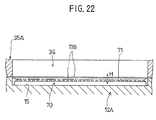
- FIG. 22 is a cleaning method of semiconductor device contactor of one embodiment of the present invention.
- FIGS. 2A to 2 C and FIG. 3 are cross-sectional diagrams showing a semiconductor device contactor 10 A (the semiconductor device contactor is hereinafter simply referred to as a contactor) of a first embodiment of the present invention.
- contactors 10 A to 10 I of the embodiments described later may be applied to any types of semiconductor chip and semiconductor device (hereinafter both are generically referred to as a semiconductor device) such as a wafer, a bare-chip, BGA (Ball Grid Array), an SOP (Small Outline Package) and a QFP (Quad Flat Package).
- a semiconductor device 20 is described as a wafer.
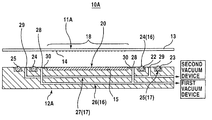
- the contactor 10 A generally includes a wiring substrate 11 A and a base unit 12 A.
- the wiring substrate 11 A includes a wiring pattern, not shown, provided on a base film 13 .
- the base film 13 is, for example, made of a resin such as polyimide (PI) and has a thickness of about 25 to 100 ⁇ m.
- the wiring pattern is made of an electrically conductive material such as a copper foil or an aluminum foil patterned into a predetermined configuration. Also, the wiring pattern is provided with contact electrodes 14 which may be electrically connected to terminals 21 provided on the semiconductor device 20 (see FIGS. 9A and 9B).
- the wiring substrate 11 A is configured such that a region in which the contact electrodes 14 will be connected to the terminals 21 of the semiconductor device 20 is flexible. Hereinafter, this region will be referred to as a connection region 18 . In order to give flexibility to the connection region 18 , the thickness of the base film 13 may be reduced at a corresponding area. Also, the wiring substrate 11 A is given a predetermined rigidity at a peripheral area of the connection region 18 .
- the base unit 12 A may be made of metal, such as aluminum and stainless steel, or of hard resin.
- the base unit 12 A is provided with a recessed mounting part 15 in which the semiconductor device 20 can be mounted.
- the base unit 12 A is further provided with a contact pressure applying mechanism 16 and a position maintaining force applying mechanism 17 .
- the contact pressure applying mechanism 16 generally includes a first seal member 24 and a first suction pipe 26 .
- the first seal member 24 may be an O-ring. As shown in FIG. 3, the first seal member 24 is provided on the base unit 12 A and surrounds the semiconductor device 20 mounted on the mounting part 15 . In detail, the first seal member 24 is provided in a first recessed part 22 which is formed in the base unit 12 A and surrounds the mounting part 15 .
- the first seal member 24 is provided in such a manner that it slightly protrudes from the top surface of the base unit 12 A. Therefore, as shown in FIGS. 2B and 2C, when the wiring substrate 11 A is mounted on the base unit 12 A, the first seal member 24 touches the wiring pattern 11 A in a hermetic manner.
- the wiring substrate 11 A when the wiring substrate 11 A is mounted on the base unit 12 A, the wiring substrate 11 A, the base unit 12 A and the first seal member 24 enclose a sealed spatial region.
- the sealed spatial region will be referred to as a first closed region 31 .
- the area of the first closed region 31 is provided so as to cover at least the above-described connection region 18 .
- the first suction pipe 26 is provided inside the base unit 12 A.
- One end of the first suction pipe 26 opens at a position between the mounting part 15 and the first seal member 24 .
- the first suction pipe 26 opens on a surface on which the semiconductor device 20 is mounted.
- this opening will be referred to as a contact pressure opening 28 . Therefore, the contact pressure opening 28 opens in the first closed region 31 .. Also, in the present embodiment, as shown in FIG. 3, four contact pressure openings 28 are provided in the first closed region 31 .
- the other end of the first suction pipe 26 extends at a side surface of the base unit 12 A and is connected to a first vacuum device which is not shown in the Figure. Therefore, by driving the first vacuum device, the first closed region 31 is vacuumed via the first suction pipe 26 . Thus, a negative pressure is built up in the first closed region 31 .
- a communication stepped portion 30 is formed at a peripheral position of the mounting part 15 .
- the communication stepped portion 30 is slightly recessed from the upper surface of the base unit 12 A.
- the mounting part 15 is also included in the first closed region 31 and a negative pressure is applied inside the mounting part 15 . Further, the negative pressure within the first closed region 31 and the mounting part 15 can be adjusted to any value by controlling the first vacuum device.
- the first closed region 31 covers the connection region 18 .
- the first vacuum device is driven with the wiring substrate 11 A being mounted on the first seal member 24 , the first closed region 31 will be brought to a negative pressure.
- the connection region 18 of the wiring substrate 11 A will be pressed towards the semiconductor device 20 . Therefore, the contact electrodes 14 of the wiring substrate 11 A can be pressed to the terminals 21 of the semiconductor device 20 .
- the negative pressure applied by the contact pressure applying mechanism 16 serves as a contact pressure for pressing the contact electrodes 14 of the wiring substrate 11 A to the terminals 21 of the semiconductor device 20 .
- the contact pressure can be adjusted to any value by controlling the first vacuum device.
- the contact pressure may be controlled by a structure. in which a number and radius of the contact pressure openings 28 can be adjusted.
- the position maintaining force applying mechanism 17 of the present embodiment generally includes a second seal member 25 and a second suction pipe 27 .
- the second seal member 25 may be an O-ring. As shown in FIG. 3, the second seal member 25 is provided on the base unit 12 A and surrounds the first seal member 24 . In detail, the second seal member 25 is provided in a second recessed part 23 which is formed in the base unit 12 A and surrounding the first seal member 24 .
- the second seal member 25 is provided in such a manner that it slightly protrudes from the top surface of the base unit 12 A.
- the second seal member 25 is protruded substantially by an equal amount to that of the first seal member 24 . Therefore, as shown in FIGS. 2B and 2C, when the wiring substrate 1 A is mounted on the base unit 12 A, the first and second seal members 24 , 25 contact the wiring pattern 11 A in a hermetic manner.
- a sealed spatial region is created by the wiring substrate 11 A, the base unit 12 A, the first seal member 24 and the second seal member 25 .
- the sealed spatial region will be referred to as a second closed region 32 .
- the second closed region 32 is a completely independent region since it is hermetically separated from the first closed region 31 by means of the first seal member 24 .
- a second suction pipe 27 is provided inside the base unit 12 A.
- One end of the second suction pipe 27 opens at a position between the first seal member 24 and the second seal member 25 .
- this opening will be referred to as a position maintaining force opening 29 . Therefore, the position maintaining force opening 29 opens in the second closed region 32 .
- eight position maintaining force openings 29 are provided in the second closed region 32 .
- the other end of the second suction pipe 27 extends at a side surface of the base unit 12 A and is connected to a second vacuum device which is not shown in the Figure. Therefore, by driving the second vacuum device, the second closed region 32 is vacuumed via the second suction pipe 27 . Thus, a negative pressure is built up in the second closed region 32 .
- the first and second vacuum devices may be integrated as a single device, but it is necessary that the first suction pipe 26 and the second suction pipe 27 can be independently adjusted to their respective degrees of vacuum.
- the negative pressure applied by the position maintaining force applying mechanism 17 serves as a contact pressure for fixedly holding the wiring substrate 11 A on the base unit 12 A.
- the position maintaining force can be adjusted to any value by controlling the second vacuum device.
- the first and second closed regions 31 , 32 are hermetically defined as describe above, it is possible to independently adjust the contact pressure applied in the first closed region 31 and the position maintaining force applied in the second closed region 32 .
- the contact pressure may be controlled by a structure in which a number and radius of the position maintaining force openings 29 can be adjusted.
- the semiconductor device 20 is mounted on the mounting part 15 of the base unit 12 A. Then, the wiring substrate 11 A is placed on the base unit 12 A in such a manner that the wiring substrate 11 A is positioned against the semiconductor device 20 . In this state, the first and second seal members 24 , 25 are in contact with the wiring substrate 11 A.
- the second vacuum device is driven so as to generate the position maintaining force (negative pressure) in the second closed region 32 .
- the position maintaining force is adjusted to a value sufficient for securely holding the wiring substrate 11 A on the base unit 12 A.
- the wiring substrate 11 A can be securely held on the base unit 12 A. However, there is no contact pressure (negative pressure) applied to the first closed region 31 . Also, since the first closed region 31 is completely independent of the second closed region 32 , the connection region 18 of the wiring substrate 11 A will be separated from the semiconductor device 20 .
- the first vacuum device is driven so as to generate the contact pressure (negative pressure) in the first closed region 31 .
- the contact pressure is adjusted to a value suitable for connecting the contact electrodes 14 and the terminals 21 .
- a good connecting state may be achieved between the contact electrodes 14 and the terminals 21 .
- the contact electrodes 14 and the terminals 21 will not be damaged during the connecting process.
- connection region 18 having the contact electrodes 14 has greater flexibility than other parts. Therefore, when the contact pressure is applied, the connection region 18 will be uniformly connected to all of the terminals 21 of the semiconductor device 20 . Therefore, even if, as in the present embodiment, the wafer is used as the semiconductor device 20 and thus there are a large number of terminals, the contact electrodes 14 of the wiring substrate 11 A can be positively connected to all of the terminals 21 , respectively.
- the contact pressure applying mechanism 16 and the position maintaining force applying mechanism 17 are provided independently. Note that the contact pressure applying mechanism 16 produces the contact pressure between the semiconductor device 20 and the wiring substrate 11 A, and the position maintaining force applying mechanism 17 produces the position maintaining force between the base unit 12 A and the wiring substrate 11 A. Therefore, the position maintaining force and the contact pressure can be controlled (operated) independently.
- the contact pressure and the position maintaining force are prevented from influencing each other. Therefore, the optimal, position maintaining force for holding the wiring substrate 11 A on the base unit 12 A and the optimal contact pressure for connecting the semiconductor device 20 to the wiring substrate 11 A can be generated independently. Thus, it is possible to achieve the accurate positioning between the wiring substrate 11 A and the base unit 12 A. Also, it is possible to keep the semiconductor device 20 and the wiring substrate 11 A in a secure and stable contact state.
- the negative pressure is used as the contact pressure between the semiconductor device 20 and the wiring substrate 11 A. Therefore, the wiring substrate 11 A can be uniformly connected to the semiconductor device 20 . That is to say, the contact pressure (i.e., negative pressure) in the first closed region 31 is uniformly applied to the inner wall of the first closed region 31 .
- the wiring substrate 11 A can be uniformly connected to the semiconductor device 20 . Therefore, even if the semiconductor device 20 is provided with a larger number of terminals, all of the terminals 21 can be securely connected to the contact electrodes 14 , respectively.
- the negative pressure is also used as the position maintaining force, so that the position maintaining force (negative pressure) is uniformly applied to the entire inner surface of the second closed region 32 . Therefore, the wiring substrate 11 A can be held on the base unit 12 A with the uniform position maintaining force. Therefore, the wiring substrate 11 A can be prevented from being tilted during mounting, and this can also achieve a stable contact state.
- a single wafer is used as the semiconductor device 20 .
- a plurality of the above-described semiconductor devices are mounted on the mounting part 15 and the wiring substrate is totally and simultaneously connected to the plurality of the semiconductor devices.
- the semiconductor device 20 is tested with such a structure, it is possible to improve a testing efficiency.
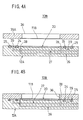
- FIGS. 4A and 4B are cross-sectional diagrams showing a contactor 10 B related to the second embodiment of the present invention.
- FIGS. 4A and 4B the same structures as those described for the contactor 10 A of the first embodiment in FIGS. 2A to 2 C and FIG. 3 will be indicated with the same reference numerals and detailed a description thereof will be omitted. This also applies to each of the embodiments described below.
- the wiring substrate 11 A is directly mounted (by suction force) on the base unit 12 A.
- the contactor 10 B of the second embodiment is characterized in that there is provided a cover unit 35 A for holding the wiring substrate 11 B.
- the cover unit 35 A is made of the same material as that of the base unit 12 A. Also, a cover unit opening 36 is provided in the central part of the base unit 12 A at an area corresponding to the connection region 18 of the wiring substrate 11 B.
- the wiring substrate 11 B of the present embodiment differs from the wiring substrate 11 A used in the first embodiment in that the wiring substrate 11 B is entirely flexible.
- the wiring substrate 11 B has an entirely uniform structure, it is possible to reduce the cost as compared to the wiring substrate 11 A.
- the wiring substrate 11 B is fixed on the lower surface (the surface opposing the base unit 12 A) of the cover unit 35 A by, for example, an adhesive agent.
- connection region 18 will also be deformed so that it is not possible to achieve a good connection.
- the wiring substrate 11 A used in the first embodiment is configured such that the peripheral part of the connection region 18 is rigid.
- the entire flexible wiring substrate 11 B is provided on the cover unit 35 A. Therefore, it is possible to connect the wiring substrate 11 B to the semiconductor device 20 with a predetermined contact pressure. Also, since the cover unit 35 A is provided with the cover unit opening 36 at a position opposing the connection region 18 , the wiring substrate 11 B remains flexible in the connection region 18 .
- the contact electrode 14 of the wiring substrate 11 B can be positively connected to all of the terminals 21 of the semiconductor device 20 .
- the second closed region 32 in which the position maintaining force is applied, opposes the lower surface of the cover unit 35 A. Therefore, even if the position maintaining force is increased, there will be no deformation produced in the wiring substrate 11 B. Therefore, the wiring substrate 11 B can be positively held on the base unit 12 A.
- FIG. 5 is a cross-sectional diagram showing the contactor 10 C of the third embodiment.
- a negative pressure is used for the position maintaining force applying mechanism 17 .
- the contactor 10 C of the third embodiment is characterized in that a fastening mechanism is used for the position maintaining force applying mechanism 17 .
- the fastening mechanism is defined as a mechanism for holding the wiring substrate on the base unit by means of a mechanically produced force.
- the fastening mechanism is realized by screws 37 . These screws will be hereinafter referred to as position maintaining force applying screws.
- the position maintaining force applying screw 37 is penetrated through a through hole provided in the cover unit 35 B.
- the base unit 12 B is provided with screw holes in which the position maintaining force applying screws 37 may be screwed.
- the cover unit 35 B is mounted on the base unit 12 B with the wiring substrate 11 B being positioned with the semiconductor device 20 , and the position maintaining force applying screw 37 is fastened.
- the cover unit 35 B (the wiring substrate 11 B) will be held on the base unit 12 B.
- the position maintaining force can be adjusted by fastening the position maintaining force applying screw 37 .
- a fastening force produced by the position maintaining force applying screws 37 serves as the position maintaining force between the wiring substrate 11 B and the base unit 12 B.
- the position maintaining force applying mechanism 17 of a comparatively simple and cost effective structure can be achieved.
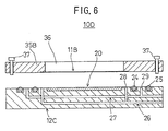
- FIG. 6 is a cross-sectional diagram showing the contactor 10 D of the fourth embodiment of the present invention.
- the present embodiment is characterized in that the position maintaining force applying mechanisms of the first and second embodiments using the negative pressure and that of the third embodiment using a fastening mechanism are combined.
- the position maintaining force applying mechanisms of the first and second embodiments using the negative pressure and that of the third embodiment using a fastening mechanism may be appropriately combined. It is not necessary to provide the position maintaining force applying mechanisms individually.
- FIGS. 7A and 7B are cross-sectional diagrams showing the contactor 10 E of the fifth embodiment.
- the contactor 10 E of the present embodiment is characterized in that the contact pressure applying mechanism 16 is used as a lifting mechanism.
- the lifting mechanism is defined as a mechanism for applying a contact pressure by moving the semiconductor unit 20 mounted on the mounting part 15 towards the wiring substrate 11 B.
- the lifting mechanism is realized by a lifting element 38 such as a piezoelectric element whose thickness may be electrically altered.
- the lifting element 38 is provided at the lower part of the mounting part 15 of the base unit 12 D. Thus, when the voltage is applied to the lifting element 38 , the semiconductor device 20 place on the lifting element 38 will move upwards. Also, by ceasing the voltage application, the semiconductor device 20 will move downwards.
- the position maintaining force applying mechanism 17 includes the first and second seal member 24 , 25 , the second suction pipe 27 , and the position maintaining force opening 29 .
- the contact pressure can be applied between the semiconductor device 20 and the wiring substrate 11 B by means of the lifting element 38 (lifting mechanism). Also, by using the contact pressure applying mechanism 16 as the lifting mechanism as in the present embodiment, it is possible to produce the contact pressure between the semiconductor device 20 and the wiring substrate 11 B with a comparatively simple structure. Note that the contact pressure can be adjusted by controlling the voltage applied to the lifting element 38 .
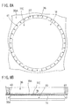
- FIGS. 8A and 8B are diagrams showing a wiring substrate 11 C provided on the contactor of the sixth embodiment.
- FIG. 8A is a flat enlarged diagram showing a neighborhood of the cover unit opening 36 of the cover unit 35 A on which the wiring substrate 11 C is provided.
- FIG. 8A is a cross-sectional diagram showing the cover unit 35 A on which the wiring substrate 11 C is provided.
- the present embodiment is characterized in that a deformable part 40 is provided at a peripheral part of the connection region 18 of the wiring substrate 11 C.
- the connection region 18 is a region in which the contact electrodes 14 are connected to the terminals 21 of the semiconductor device 20 .
- the deformable part 40 is constructed by a plurality of small holes 41 provided along the periphery of the connection region 18 .
- the small holes 41 may be formed by various methods including etching, punching, and laser processing.
- a back-up sheet 39 A is provided on the back surface of the wiring substrate 11 C.
- the peripheral part of the wiring substrate 11 C will be more flexible.
- the position of the deformable part 40 is not limited to the peripheral part of the connection region 18 , but may also be at the position opposing the region in which the terminals 21 of the semiconductor device 20 are not formed.
- the deformable part 40 is not limited to a structure using the small holes 41 , but can be achieved by reducing the thickness of the base film 13 by, for example, etching.
- FIGS. 9A and 9B are enlarged cross-sectional diagrams showing a wiring substrate 11 D provided on the contactor of the seventh embodiment.
- FIG. 9A is an enlarged diagram showing a neighboring part of the cover unit opening 36 of the cover unit 35 A on which the wiring substrate 11 D is provided.
- FIG. 9B is an enlarged diagram showing the wiring substrate 11 D being in a connected state with the terminals 21 of the semiconductor device 20 .
- the wiring substrate 11 D includes a plurality of laminated wiring layers.
- two wiring layers 42 A, 42 B are illustrated.
- the wiring layers 42 A, 42 B are provided with contact electrodes 14 A, 14 B which are selectively connected to the terminals 21 of the semiconductor device 20 .
- the contact electrodes 14 A, 14 B are provided on respective base films 13 A, 13 B.
- the terminals 21 of the semiconductor device 20 are configured as bumps.
- the wiring substrate 11 D is provided with insert holes 43 provided at predetermined positions to be connected to the terminals 21 of the semiconductor device 20 .
- the contact electrodes 14 A, 14 B to be connected to the terminals 21 corresponding to the insert hole positions are provided so as to extend in the insert holes 43 . Therefore, when the wiring substrate 11 D is electrically connected to the semiconductor device 20 , the terminals 21 made of bumps will be inserted in the insert holes 43 . Thereby the terminals 21 will be connected to the predetermined contact electrodes 14 A, 14 B, thus achieving an electrical conduction.
- an increased number of contact electrodes 14 A, 14 b can be provided compared to a single layered wiring substrate. Therefore, the contactor can still be used with the high-density semiconductor device 20 having an increased number of terminals.
- FIG. 10 is an enlarged cross-sectional diagram showing a wiring substrate 11 E provided on the contactor of the eighth embodiment.
- the wiring substrate 11 E is provided with through holes 44 serving as conducting-parts.
- the surface of the wiring substrate 11 E on which the semiconductor is connected will be referred to as a connecting surface 11 E- 1 .
- the surface opposite to the connecting surface 11 E- 1 will be referred to as an opposite surface, 11 E- 2 .
- the present embodiment is characterized in that the connecting surface 11 E-i and the opposite surface 11 E- 2 are electrically connected by the through holes 44 .
- FIG. 11 is an enlarged cross-sectional diagram showing the wiring substrate 11 E provided on the contactor of the ninth embodiment.
- the present embodiment is characterized in that the wiring substrate 11 E used in the eight embodiment is utilized together with electronic components 45 mounted on the opposite surface 11 E- 2 .
- the electronic components 45 may be elements such as a capacitor, a resistor, a fuse, and a self burn-in-circuit.
- the wiring substrate itself has a function of implementing a test on the semiconductor device 20 .
- FIGS. 12A and 12B are enlarged cross-sectional diagrams showing the wiring substrate 11 B provided on the contactor of the tenth embodiment.
- the present embodiment is characterized in that a tension applying mechanism 46 is provided for applying a predetermined tension F on the wiring substrate 11 B.
- the tension applying mechanism 46 includes a tapered surface 47 , an accommodation recess 48 and a protruded component 49 .
- the tapered surface 47 is provided on the surface of the cover unit 35 C opposing the base unit 12 A (not shown in FIGS. 12A and 12B).
- the accommodation recess 48 is formed at a part of the tapered surface 47 .
- the protruded component 49 has a protrusion 49 A to be fitted into the accommodation recess 48 .
- FIG. 13 is a cross-sectional diagram showing the contactor 10 F of the eleventh embodiment.
- the contact pressure applying mechanism 16 and the position maintaining force applying mechanism 17 are omitted from the figure.
- the present embodiment is characterized in that a base unit 12 E has a heat dissipation function.
- the base unit 12 E is made of a material with good thermal conductivity and is provided with a heat dissipation fin part 50 .
- FIG. 14 is a cross-sectional diagram showing the contactor 10 G of the twelfth embodiment.
- the contact pressure applying mechanism 16 and the position maintaining force applying mechanism 17 are omitted from the figure.
- the present embodiment is characterized in that a base unit 12 G is provided with a temperature controlling device 51 .
- the temperature controlling device 51 internally includes at least one of a temperature applying mechanism, a heat absorption mechanism and a temperature detecting mechanism.
- the temperature controlling device 51 provided in the base unit 12 E the temperature of the semiconductor device 20 during the test can be adjusted to a proper temperature. Also, it is possible to adjust any positioning offset due to thermal expansion of the base unit 12 E.
- the temperature applying mechanism may be an electric heater and the heat absorption mechanism may be, for example, a Peltier element.
- FIG. 15 is a cross-sectional diagram showing the contactor 10 H of the thirteenth embodiment.
- the contactor 10 H of the present embodiment is characterized in that a base unit 12 G is provided with a holding mechanism 52 for forcing the semiconductor device 20 to be held on the mounting part 15 .
- the holding mechanism 52 is formed by a holding suction pipe 53 provided in the base unit 12 G.
- One end of the holding suction pipe 53 opens in the mounting part 15 .
- the opening will be referred to as a semiconductor device holding opening 53 A.
- the other end of the holding suction pipe 53 is pulled out at a side surface of the base unit 12 G and is connected to a third vacuum device which is not shown in the Figure.
- the semiconductor device 20 mounted on the mounting part 15 is vacuumed at the semiconductor device holding opening 53 A.
- the semiconductor device 20 is held on the base unit 12 G.
- the semiconductor device 20 can be fixed to the base unit 12 G before positioning the wiring substrate 11 B (cover unit 35 A) and the base unit 12 G. Thereafter, the semiconductor device 20 is prevented from being displaced in the mounting part 15 , so that the positioning can be achieved with a higher accuracy. (Note that there a small gap between the mounting part 15 and the semiconductor device 20 for facilitating the attachment and removal of the semiconductor device 20 .)
- the wafer when used as the semiconductor device 20 , there may be a warp in the wafer.
- a plurality of the semiconductor device holding openings 53 A can be formed in the mounting part.
- the back surface of the mounted wafer semiconductor device 20
- the back surface of the mounted wafer may be entirely and uniformly vacuumed so as to correct the warp of the wafer-(semiconductor device 20 ).
- FIG. 16 is a cross-sectional diagram showing the contactor 10 I of the fourteenth embodiment.
- the contactor 10 I of the present embodiment is characterized in that at least one of the wiring substrate 11 B, the cover unit 35 A, and the base unit 12 A is provided with a friction increasing part for increasing the friction produced between the wiring substrate 11 B (cover unit 35 A) and the base unit 12 A.
- the friction increasing part is a friction increasing sheet 54 having a comparatively high friction coefficient (e.g., rubber) at the surface. Also, the friction increasing sheet 54 is provided around the wiring substrate 11 B.
- the friction increasing sheet 54 serves as the friction increasing part.
- the friction increasing part is not limited but can be made by directly forming a coarse surface on the cover unit and the base unit.
- FIG. 17 is an enlarged diagram showing a neighborhood of the wiring substrate 11 B provided on the contactor of the fifteen the embodiment.
- the contactor 10 I of the present invention is provided with a third seal member 55 between the wiring substrate 11 A and the cover unit 35 A and a forth seal member 56 provided in a base unit 12 H.
- a third seal member 55 between the wiring substrate 11 A and the cover unit 35 A
- a forth seal member 56 provided in a base unit 12 H.
- the third seal member 55 is a sheet-like seal member, and can be made of a resin of such as a silicon type or a fluorine type.
- the forth seal member 56 is for example sphere-like and can be made of a resin of such as the silicon type or the fluorine type.
- the forth seal member 56 is provided in the contact pressure opening 28 of the first suction pipe 26 .
- the contact pressure opening 28 communicates with the mounting part 15 via the communication stepped part 30 . Therefore, when applying the contact pressure in the first closed region 31 , the fourth seal member 56 will not be obstructive.
- FIG. 18 is an enlarged diagram showing a neighborhood of the wiring substrate 11 B provided on the contactor of the sixteenth embodiment.
- the present embodiment is characterized in that a back-up sheet 39 B having protrusions and recesses is provided on the opposite surface of the wiring substrate 11 B (the surface opposite to the surface connected to the semiconductor device 20 ).
- the back-up sheet 39 B is made of an elastic material such as silicon rubber and is provided with protrusions at positions opposing the contact electrodes 14 .
- the back-up sheet 39 B having a certain elasticity, any variation between the heights of the terminals 21 of the semiconductor device 20 or the contact electrodes 14 of the wiring substrate 11 B will be compensated for by a deformation of the back-up sheet 39 B.
- the back-up sheet 39 B will produce an elastic restoration force by being pressed with the terminals 21 . Therefore, this elastic restoration force serves as the contact pressure.
- the contact pressure is also produced in the back-up sheet 39 B, it is possible to implement a more stable connection.
- FIG. 19 is schematic diagram of a testing apparatus 60 of an embodiment of the present invention.
- the testing apparatus 60 includes the contactor 10 B, a testing apparatus chamber 61 and a compressed air producing device 62 .
- the contactor 10 B is the contactor of the second embodiment described above by reference to FIG. 4.
- the contactor available for the testing apparatus 60 is not limited to the contactor 10 B of the second embodiment, but can be any one of the contactors described above.
- the testing apparatus chamber 61 is an airtight container and the contactor 10 B is installed therein. With the contactor 10 B being installed in the testing apparatus chamber 61 , the first and second suction pipe 26 , 27 extend outside the testing apparatus 60 and are connected to the first and second vacuum devices. In the figure, the contactor 10 B is mounted on a base table 63 .
- the compressed air producing device 62 includes a compression pump, and can introduce compressed air into the testing apparatus chamber 61 . Therefore, by driving the compression air-producing device 62 , the pressure within the testing apparatus chamber 61 will become a positive pressure.
- the testing apparatus 60 of the present embodiment includes the testing apparatus chamber 61 having an internal atmosphere brought to a positive pressure by the compressed air producing device 62 provided thereon and the contactor 10 B installed in the testing apparatus chamber 61 . Therefore, it is possible-to securely connect the contact electrodes 14 to the terminals 21 even when the contact pressure due to the negative pressure produced in the first closed region 31 is insufficient.
- the semiconductor device 20 is mounted on the mounting part 15 of the base unit 12 A. Then, as shown in FIG. 20, a position recognition process of the terminals 21 of the semiconductor device 20 and the contact electrodes 14 of the wiring substrate 11 B is implemented by means of a CCD camera 65 A. Here, the terminals 21 and the contact electrodes 14 are not shown in the figure.
- the CCD camera 65 A of the present embodiment is capable of imaging both directions in its upper and lower side. Therefore, since the recognition process of the terminals 21 and the contact electrodes 14 can be implemented simultaneously, the time required for the recognition process is reduced.
- the positioning of the wiring substrate 11 B and the base unit 12 A is implemented.
- the position maintaining force applying mechanism 17 is driven so as to produce a negative pressure in the second closed region 32 .
- the position maintaining force is produced between the wiring substrate 11 B (cover unit 35 A) and the base unit 12 A.
- the wiring substrate 11 and the semiconductor device 20 will be maintained in a positioned state.
- the contact pressure applying mechanism 16 is driven so as to produce a negative pressure in the first closed region 31 .
- the contact pressure is applied between the wiring substrate 11 B and the semiconductor device 20 .
- the wiring substrate 11 B will be connected to the semiconductor device 20 so that the predetermined test can be implemented.
- the position recognition process of the terminals 21 of the semiconductor device 20 and the contact electrodes 14 is implemented. Then, the wiring substrate 11 B and the semiconductor device 20 (base unit 12 A) are positioned based on the position correction value obtained from the position recognition process. Thus, according to the testing method of the present embodiment, the positioning can be implemented with a comparatively high accuracy.
- the position maintaining force applying mechanism 17 is driven so as to apply a position maintaining force between the wiring substrate 11 B and the base unit 12 A.
- the position maintaining force applying mechanism 17 is driven so as to apply a position maintaining force between the wiring substrate 11 B and the base unit 12 A.
- a CCD camera 65 A which is capable of imaging both directions in its upper and lower side.
- the recognition process is implemented by moving this CCD camera 65 A between the wiring substrate 11 B and the semiconductor device 20 .
- the CCD camera 65 A which can image both directions in its upper and lower sides is expensive. Also, an operability is not particularly good when moving the CCD camera 65 A between the wiring substrate 11 B and the semiconductor device 20 during the recognition process.
- the present embodiment is characterized in that a CCD camera 65 B is placed above the cover unit 35 A.
- the semiconductor device 20 can be positioned by looking through the wiring substrate 11 B from above.
- a transparent PI tape is used for the wiring substrate 11 B such that the semiconductor device 20 can seen through the wiring substrate 11 B.
- the CCD camera 65 B can be of a simple and cheap structure capable of imaging only one direction, since there is not a need for vertical imaging as is required for the method of the first embodiment.
- the method of cleaning according to the present embodiment can be applied to any one of the contactors 10 A to 10 I of the above-described embodiments.
- the method of the present embodiment is for implementing a cleaning process of the contact electrodes 14 of the wiring substrates 11 A to 11 E provided on the respective contactors 10 A to 10 I.
- a method of implementing a cleaning process of the contactor 10 B of the second embodiment will be described.
- a cleaning member 70 is mounted on the mounting part 15 provided in the base unit 12 A.
- the cleaning member 70 may be a wrapping sheet with fine protrusions and recesses 71 .
- the contact pressure applying mechanism 16 is repeatedly driven and stopped. Thereby, the first closed area 31 is alternately and repeatedly brought to a state in which the contact pressure is applied and a state in which the contact pressure is not applied. In other words, the wiring substrate 11 A will vibrate in the direction indicated with an arrow H in the figure.
- the cleaning member 70 will be repeatedly in contact with, slide on or collide with the contact electrodes 14 provided on the wiring substrate 11 B.
- unnecessary layers such as an oxidization layer disposed on the contact electrodes 14 can be removed by means of the cleaning member 70 .
- the contact electrodes 14 can be always kept in a good state, and it is possible to improve the reliability of the electric connection of the wiring substrate 11 B against the semiconductor device 20 .
Abstract
Description
- 1. Field of the Invention
- The present invention generally relates to a contactor for semiconductor devices, a testing apparatus using such a contactor, a testing method using such a contactor and a method of cleaning such a contactor, and particularly relates to a contactor for obtaining an electrical contact with a semiconductor device such as a wafer, a bare chip, a BGA (Ball Grid Array), an SOP (Small Outline Package) and a QFP (Quad Flat Package), a testing apparatus and a testing method using the contactor, and a method of cleaning such a contactor.
- Recently, there is an increasing need for further miniaturized, high-speed and high-density semiconductor devices. Therefore, in order to provide terminals corresponding with such semiconductor devices, efforts are being made to achieve a further fine-pitched structure of the terminals provided on the semiconductor devices. Also, in order to improve the testing efficiency of the semiconductor devices, there is a need for simultaneously contacting a plurality of semiconductor devices, for example, at a wafer level.
- However, the height of the terminals of the semiconductor devices and the height of contact electrodes are varied. Therefore, it is technically very difficult to connect the contact electrodes to all of the fine-pitched terminals.
- 2. Description of the Related Art
- FIG. 1 is a cross-sectional diagram showing a
contactor 1 for a semiconductor device (hereinafter referred to as a contactor) of the related art. As shown in the Figure, thecontactor 1 includes awiring substrate 2, an anisotropic conductive sheet 4, amultilayer substrate 5, and a base member 6. - The
wiring substrate 2 includes a base film made of resin and a wiring pattern formed thereon. Also, a part of the wiring pattern is provided with contact electrodes 3 to which terminals of a semiconductor device 8 (in the Figure, a wafer is illustrated as an example of the semiconductor device) are connected. The contact electrodes 3 extend to an upper surface (i.e., a surface opposite a surf ace provided with the contact electrodes 3) of thewiring substrate 2 via through holes or vias (not shown) formed in the base film. - The
multilayer substrate 5 is a multilayer wiring printed-circuit board, which includes a substrate made of glass-epoxy whereon a plurality of wiring substrate layers provided with wiring patterns are laminated. Also, the layers provided with the wiring patterns are each electrically connected by elements such as through holes. Therefore, in the related art, themultilayer substrate 5 is made of an extremely hard material (or a material with a high rigidity). - In the
contactor 1 shown in the Figure, the anisotropic conductive sheet 4 is provided between thewiring substrate 2 and themultilayer substrate 5. The anisotropic conductive sheet 4 is elastic and is conductive in a vertical direction in the Figure, so that an electric connection is established only at only at locations under pressure. - If the
wiring substrate 2 is provided directly on themultilayer substrate 5 with high rigidity, it is not possible to overcome the variation of the heights of the terminals of the semiconductor device 8 or the contact electrodes 3 of thewiring substrate 2. The purpose of using the anisotropic conductive sheet 4 is to avoid such a drawback and thus positively connect the contact electrodes 3 to the plurality of terminals. Also, thewiring substrate 2, the anisotropic conductive sheet 4 and themultilayer substrate 5 constitute an integrated body. - The base, member 6 is provided with a mounting portion 7 having a recessed shape corresponding to the contour of the semiconductor device 8. The semiconductor device 8 is mounted in the mounting portion 7 so as to be maintained by the base member 6.
- For electrically connecting the
contactor 1 of the above structure and the semiconductor device 8, the semiconductor device 8 is mounted on the mounting portion 7 of the base member 6. Then, thewiring substrate 2 is pressed onto the semiconductor device 8. Thus, the contact electrodes 3 and the terminals of the semiconductor device 8 are connected and it is possible to establish an electrical conduction between thewiring substrate 2 and the semiconductor device 8. - In FIG. 1, the
contactor 1 includes the anisotropic conductive sheet 4 provided between thewiring substrate 2 and themultilayer substrate 5. However another example of the contactor of the related art may include an anisotropic conductive sheet provided between a wiring substrate and a semiconductor device. - Also, there is provided a contactor with greater contact pressure (adhesive force) between the wiring substrate and the semiconductor device. This is achieved by providing a seal member between a base member on which the semiconductor device wafer is mounted and the wiring substrate. A negative pressure is built,up in an area sealed with the sealing member so that the wiring substrate will be pressed against the semiconductor wafer under atmospheric pressure.
- There are two forces required for connecting the
wiring substrate 2 to the semiconductor device 8. One of the forces is a pressure required for connecting the contact electrodes 3 provided on thewiring substrate 2 to the terminals of the semiconductor device 8. This force is hereinafter referred to as a contact pressure. The other force is a pressure required for maintaining thewiring substrate 2 in position with the base member 6. This force is hereinafter referred to as a position maintaining force. - Since the contact pressure and the position maintaining force have different functions, as has been described above, it is necessary to adjust each force to a strength appropriate for the respective functions.
- That is to say, the contact pressure should be adjusted for providing a good electrical connection between the contact electrodes 3 of the
wiring substrate 2 and the terminals of the semiconductor device 8, thus preventing any deformation of the contact electrodes 3 and the terminals. Also, the position maintaining force should be adjusted to a value sufficient for preventing any offset of the positioning of thewiring substrate 2 and the base member 6 when there is a certain external force being applied. - Therefore, for electrically connecting the
wiring substrate 2 and the semiconductor device 8 in an ideal state, normally, it is necessary that the strength of the position maintaining force be greater than that of the contact pressure. - However, with the
contactor 1 of the related art, the contact pressure and the position maintaining force cannot be adjusted independently. With such a structure, the wiring substrate and the semiconductor devices may be electrically connected by the above-described negative pressure. Then, if the negative pressure is released in order to release the contact pressure, the position maintaining force is also released. Accordingly, there is a drawback that the wiring substrate and the semiconductor devices are offset from the predetermined positions. - Also, with the
contactor 1 of the related art, the contact pressure and the position maintaining force are the same force. When it is attempted to increase the position maintaining force, the contact pressure will also be increased, thus creating a risk of the terminals of the semiconductor device being seriously damaged. - Further, with the
contactor 1 of the related art, the flexibility of thewiring substrate 2 is provided by the elasticity of the anisotropic conductive sheet 4 and thus is limited to such elasticity. Therefore, it is not possible to compensate for any variation of heights of the contact electrodes 3 and the terminals which variation exceeds the elasticity of the anisotropic conductive sheet 4. Accordingly, when there is any variation of the heights of the fine-pitched terminals, the contact electrodes 3 cannot be connected to all of the terminals of the semiconductor device 8. - Accordingly, it is a general object of the present invention to provide a semiconductor device contactor which can solve the problems described above. It is another and more specific object of the present invention to provide a semiconductor device contactor which can securely connect contact electrodes to a semiconductor device having fine terminals and can prevent the terminals and the contact electrodes from being damaged.
- In order to achieve the above objects according to the present invention, a semiconductor device contactor includes a base unit for holding a semiconductor device provided with a plurality of terminals and a wiring substrate provided with contact electrodes at positions corresponding to at least some of the terminals. The contact electrodes and the terminals are electrically connected when the wiring substrate is held on the base unit.
- The semiconductor device contactor further includes: a position maintaining force applying mechanism for applying a position maintaining force between the base unit and the wiring substrate; and a contact pressure applying mechanism for applying a contact pressure between the semiconductor device and the wiring substrate. The position maintaining force applying mechanism and the contact pressure applying mechanism are operable in an independent manner.
- With the contactor described above, it is possible to prevent a mutual influence between the contact pressure and the position maintaining force. Thus, it is possible to independently applying an optimum position maintaining force and an optimum contact pressure. Accordingly, a precise positioning between the wiring substrate and the base unit and a stable contact state between the semiconductor device and the wiring substrate can be achieved.
- It is still another object of the present invention to provide a testing device for obtaining a stable contact force.
- In order to achieve the above object, the testing device includes a semiconductor device contactor as described above and a chamber for accommodating the semiconductor device contactor. The chamber is constructed such that its internal atmosphere may be of a positive pressure.
- With the testing device described above, even if the contact pressure resulting from the negative pressure is insufficient, the contact pressure can be relatively increased by applying a high pressure in an atmosphere of the chamber. Thus, a stable contact pressure can be obtained.
- It is yet another object of the present invention to provide a method of testing a semiconductor device using a semiconductor device contactor described above, which method can implement an accurate positioning and a secure connection of the contact electrodes of the wiring substrate to the terminals of the semiconductor device.
- In order to achieve the above object, the testing method includes the steps of:
- a) calculating a position correction value by recognizing the positions of the terminals and the electrodes, and then calculating the offset between the positions of the terminals and the contact electrodes;
- b) positioning the wiring substrate with the base unit based on the position correction value;
- c) driving, after the step b), the position maintaining force applying mechanism for applying a position maintaining force between the wiring substrate and the base unit;
- d) driving the contact pressure applying mechanism for applying a contact pressure between the wiring substrate and the semiconductor device; and
- e) testing the semiconductor device.
- With the testing method described above, an accurate positioning can be achieved by the steps a) and b). Also, a secure connection of the contact electrodes to the terminals can be achieved since, after positioning, first, the wiring substrate and the base unit are fixed by means of the position maintaining force applying mechanism and, then, the contact pressure is applied between the wiring substrate and the semiconductor device by means of the contact pressure applying mechanism.
- It is yet another object of the present invention to provide a method of cleaning the semiconductor device contactor described above which method can remove unwanted layers disposed on the contact electrodes and thus achieve a stable contact state.
- In order to achieve the above object, a method of cleaning a contactor for semiconductor devices, particularly cleaning contact electrodes provided on a wiring substrate provided on the contactor, includes the steps of:
- a) providing a cleaning member instead of the semiconductor device on the base unit, such that the cleaning member is in contact with the contact electrodes for cleaning the contact electrodes;
- b) holding the wiring substrate on the base unit by driving the position maintaining force applying mechanism;
- c) repeatedly driving and ceasing the contact pressure applying mechanism while the wiring substrate is held on the base unit.
- With the cleaning method described above, unwanted layers disposed on the contact electrodes can be remove and thus a stable contact state can be achieved.
- Other objects and further features of the present invention will be apparent from the following detailed description when read in conjunction with the accompanying drawings.
- FIG. 1 is a cross-sectional diagram showing a contactor of the related art.
- FIGS. 2A to 2C are cross-sectional diagrams showing a contactor of a first embodiment of the present invention taken along line I-I in FIG. 3.
- FIG. 3 is a plan view showing a base unit constituting the contactor of the first embodiment of the present invention.
- FIGS. 4A and 4B are cross-sectional diagrams showing a contactor of a second embodiment of the present invention.
- FIG. 5 is a cross-sectional diagram showing a contactor of a third embodiment of the present invention.
- FIG. 6 is a cross-sectional diagram showing a contactor of a fourth embodiment of the present invention.
- FIGS. 7A and 7B are cross-sectional diagrams showing a contactor of a fifth embodiment of the present invention.
- FIGS. 8A and 8B are a plan view and a cross-sectional diagram, respectively, showing a contactor of a sixth embodiment of the present invention.
- FIGS. 9A and 9B are cross-sectional diagrams showing a contactor of a seventh embodiment of the present invention.
- FIG. 10 is a cross-sectional diagram showing a contactor of an eighth embodiment of the present invention.
- FIG. 11 is a cross-sectional diagram showing a contactor of a ninth embodiment of the present invention.
- FIGS. 12A and 12B are cross-sectional diagrams showing a contactor of a tenth embodiment of the present invention.
- FIG. 13 is a cross-sectional diagram showing a contactor of an eleventh embodiment of the present invention.
- FIG. 14 is a cross-sectional diagram showing a contactor of a twelfth embodiment of the present invention.
- FIG. 15 is a cross-sectional diagram showing a contactor of a thirteenth embodiment of the present invention.
- FIG. 16 is a cross-sectional diagram showing a contactor of a fourteenth embodiment of the present invention.
- FIG. 17 is a cross-sectional diagram showing a contactor of a fifteenth embodiment of the present invention.
- FIG. 18 is a cross-sectional diagram showing a contactor of a sixteenth embodiment of the present invention.
- FIG. 19 is a cross-sectional diagram showing a testing apparatus of one embodiment of the present invention, the testing apparatus utilizing a contactor.
- FIG. 20 is a cross-sectional diagram showing a testing apparatus utilizing the contactor of the first embodiment of the present invention.
- FIG. 21 is a cross-sectional diagram showing a testing apparatus utilizing the contactor of the second embodiment of the present invention.
- FIG. 22 is a cleaning method of semiconductor device contactor of one embodiment of the present invention.
- In the following, principles and embodiments of the present invention will be described with reference to the accompanying drawings.
- FIGS. 2A to 2C and FIG. 3 are cross-sectional diagrams showing a
semiconductor device contactor 10A (the semiconductor device contactor is hereinafter simply referred to as a contactor) of a first embodiment of the present invention. - Note that contactors 10A to 10I of the embodiments described later may be applied to any types of semiconductor chip and semiconductor device (hereinafter both are generically referred to as a semiconductor device) such as a wafer, a bare-chip, BGA (Ball Grid Array), an SOP (Small Outline Package) and a QFP (Quad Flat Package). However, in the following description, by way of example, a
semiconductor device 20 is described as a wafer. - The
contactor 10A generally includes awiring substrate 11A and abase unit 12A. - The
wiring substrate 11A includes a wiring pattern, not shown, provided on abase film 13. Thebase film 13 is, for example, made of a resin such as polyimide (PI) and has a thickness of about 25 to 100 μm. The wiring pattern is made of an electrically conductive material such as a copper foil or an aluminum foil patterned into a predetermined configuration. Also, the wiring pattern is provided withcontact electrodes 14 which may be electrically connected toterminals 21 provided on the semiconductor device 20 (see FIGS. 9A and 9B). - The
wiring substrate 11A is configured such that a region in which thecontact electrodes 14 will be connected to theterminals 21 of thesemiconductor device 20 is flexible. Hereinafter, this region will be referred to as aconnection region 18. In order to give flexibility to theconnection region 18, the thickness of thebase film 13 may be reduced at a corresponding area. Also, thewiring substrate 11A is given a predetermined rigidity at a peripheral area of theconnection region 18. - The
base unit 12A may be made of metal, such as aluminum and stainless steel, or of hard resin. Thebase unit 12A is provided with a recessed mountingpart 15 in which thesemiconductor device 20 can be mounted. Thebase unit 12A is further provided with a contactpressure applying mechanism 16 and a position maintainingforce applying mechanism 17. - The contact
pressure applying mechanism 16 generally includes afirst seal member 24 and afirst suction pipe 26. - The
first seal member 24 may be an O-ring. As shown in FIG. 3, thefirst seal member 24 is provided on thebase unit 12A and surrounds thesemiconductor device 20 mounted on the mountingpart 15. In detail, thefirst seal member 24 is provided in a first recessedpart 22 which is formed in thebase unit 12A and surrounds the mountingpart 15. - Also, the
first seal member 24 is provided in such a manner that it slightly protrudes from the top surface of thebase unit 12A. Therefore, as shown in FIGS. 2B and 2C, when thewiring substrate 11A is mounted on thebase unit 12A, thefirst seal member 24 touches thewiring pattern 11A in a hermetic manner. - In other words, when the
wiring substrate 11A is mounted on thebase unit 12A, thewiring substrate 11A, thebase unit 12A and thefirst seal member 24 enclose a sealed spatial region. Hereinafter, the sealed spatial region will be referred to as a firstclosed region 31. The area of the firstclosed region 31 is provided so as to cover at least the above-describedconnection region 18. - Also, the
first suction pipe 26 is provided inside thebase unit 12A. One end of thefirst suction pipe 26 opens at a position between the mountingpart 15 and thefirst seal member 24. In other words, thefirst suction pipe 26 opens on a surface on which thesemiconductor device 20 is mounted. Hereinafter, this opening will be referred to as acontact pressure opening 28. Therefore, the contact pressure opening 28 opens in the firstclosed region 31.. Also, in the present embodiment, as shown in FIG. 3, fourcontact pressure openings 28 are provided in the firstclosed region 31. - The other end of the
first suction pipe 26 extends at a side surface of thebase unit 12A and is connected to a first vacuum device which is not shown in the Figure. Therefore, by driving the first vacuum device, the firstclosed region 31 is vacuumed via thefirst suction pipe 26. Thus, a negative pressure is built up in the firstclosed region 31. - It is to be noted that a communication stepped
portion 30 is formed at a peripheral position of the mountingpart 15. The communication steppedportion 30 is slightly recessed from the upper surface of thebase unit 12A. Thus, the mountingpart 15 is also included in the firstclosed region 31 and a negative pressure is applied inside the mountingpart 15. Further, the negative pressure within the firstclosed region 31 and the mountingpart 15 can be adjusted to any value by controlling the first vacuum device. - As has been described above, the first
closed region 31 covers theconnection region 18. When the first vacuum device is driven with thewiring substrate 11A being mounted on thefirst seal member 24, the firstclosed region 31 will be brought to a negative pressure. Theconnection region 18 of thewiring substrate 11A will be pressed towards thesemiconductor device 20. Therefore, thecontact electrodes 14 of thewiring substrate 11A can be pressed to theterminals 21 of thesemiconductor device 20. - Here, the negative pressure applied by the contact
pressure applying mechanism 16 serves as a contact pressure for pressing thecontact electrodes 14 of thewiring substrate 11A to theterminals 21 of thesemiconductor device 20. Also, as has been described above, the contact pressure can be adjusted to any value by controlling the first vacuum device. When the power of the first vacuum device is constant, the contact pressure may be controlled by a structure. in which a number and radius of thecontact pressure openings 28 can be adjusted. - The position maintaining
force applying mechanism 17 of the present embodiment generally includes asecond seal member 25 and asecond suction pipe 27. Thesecond seal member 25 may be an O-ring. As shown in FIG. 3, thesecond seal member 25 is provided on thebase unit 12A and surrounds thefirst seal member 24. In detail, thesecond seal member 25 is provided in a second recessedpart 23 which is formed in thebase unit 12A and surrounding thefirst seal member 24. - Also, the
second seal member 25 is provided in such a manner that it slightly protrudes from the top surface of thebase unit 12A. Thesecond seal member 25 is protruded substantially by an equal amount to that of thefirst seal member 24. Therefore, as shown in FIGS. 2B and 2C, when the wiring substrate 1A is mounted on thebase unit 12A, the first andsecond seal members wiring pattern 11A in a hermetic manner. - In other words, when the
wiring substrate 11A is mounted on thebase unit 12A, a sealed spatial region is created by thewiring substrate 11A, thebase unit 12A, thefirst seal member 24 and thesecond seal member 25. Hereinafter, the sealed spatial region will be referred to as a secondclosed region 32. The secondclosed region 32 is a completely independent region since it is hermetically separated from the firstclosed region 31 by means of thefirst seal member 24. - Also, a
second suction pipe 27 is provided inside thebase unit 12A. One end of thesecond suction pipe 27 opens at a position between thefirst seal member 24 and thesecond seal member 25. Hereinafter, this opening will be referred to as a position maintainingforce opening 29. Therefore, the position maintaining force opening 29 opens in the secondclosed region 32. Also, in the present embodiment, as shown in FIG. 3, eight position maintainingforce openings 29 are provided in the secondclosed region 32. - The other end of the
second suction pipe 27 extends at a side surface of thebase unit 12A and is connected to a second vacuum device which is not shown in the Figure. Therefore, by driving the second vacuum device, the secondclosed region 32 is vacuumed via thesecond suction pipe 27. Thus, a negative pressure is built up in the secondclosed region 32. - The first and second vacuum devices may be integrated as a single device, but it is necessary that the
first suction pipe 26 and thesecond suction pipe 27 can be independently adjusted to their respective degrees of vacuum. - In the above-described structure, when the second vacuum device is driven with the
wiring substrate 11A being mounted on the first andsecond seal members closed region 32 will be brought to a negative pressure. Thewiring substrate 11A will be pressed towards thebase unit 12A. Therefore, thewiring substrate 11A can be held (fixed) on thebase unit 12A. - Here, the negative pressure applied by the position maintaining
force applying mechanism 17 serves as a contact pressure for fixedly holding thewiring substrate 11A on thebase unit 12A. Also, as has been described above, the position maintaining force can be adjusted to any value by controlling the second vacuum device. Further, since the first and secondclosed regions closed region 31 and the position maintaining force applied in the secondclosed region 32. When the power of the second vacuum device is constant, the contact pressure may be controlled by a structure in which a number and radius of the position maintainingforce openings 29 can be adjusted. - In order to implement a contact process of the
semiconductor device 20 using thecontactor 10A, first, thesemiconductor device 20 is mounted on the mountingpart 15 of thebase unit 12A. Then, thewiring substrate 11A is placed on thebase unit 12A in such a manner that thewiring substrate 11A is positioned against thesemiconductor device 20. In this state, the first andsecond seal members wiring substrate 11A. - Subsequently, the second vacuum device is driven so as to generate the position maintaining force (negative pressure) in the second
closed region 32. The position maintaining force is adjusted to a value sufficient for securely holding thewiring substrate 11A on thebase unit 12A. - Thus, the
wiring substrate 11A can be securely held on thebase unit 12A. However, there is no contact pressure (negative pressure) applied to the firstclosed region 31. Also, since the firstclosed region 31 is completely independent of the secondclosed region 32, theconnection region 18 of thewiring substrate 11A will be separated from thesemiconductor device 20. - Then, in order to connect the
contact electrodes 14 of thewiring substrate 11A and theterminals 21 of thesemiconductor device 20, the first vacuum device is driven so as to generate the contact pressure (negative pressure) in the firstclosed region 31. The contact pressure is adjusted to a value suitable for connecting thecontact electrodes 14 and theterminals 21. Thus, a good connecting state may be achieved between thecontact electrodes 14 and theterminals 21. Also, thecontact electrodes 14 and theterminals 21 will not be damaged during the connecting process. - Further, in the present embodiment, the
connection region 18 having thecontact electrodes 14 has greater flexibility than other parts. Therefore, when the contact pressure is applied, theconnection region 18 will be uniformly connected to all of theterminals 21 of thesemiconductor device 20. Therefore, even if, as in the present embodiment, the wafer is used as thesemiconductor device 20 and thus there are a large number of terminals, thecontact electrodes 14 of thewiring substrate 11A can be positively connected to all of theterminals 21, respectively. - As has been described above, in the
contactor 10A of the present embodiment, the contactpressure applying mechanism 16 and the position maintainingforce applying mechanism 17 are provided independently. Note that the contactpressure applying mechanism 16 produces the contact pressure between thesemiconductor device 20 and thewiring substrate 11A, and the position maintainingforce applying mechanism 17 produces the position maintaining force between thebase unit 12A and thewiring substrate 11A. Therefore, the position maintaining force and the contact pressure can be controlled (operated) independently. - The contact pressure and the position maintaining force are prevented from influencing each other. Therefore, the optimal, position maintaining force for holding the
wiring substrate 11A on thebase unit 12A and the optimal contact pressure for connecting thesemiconductor device 20 to thewiring substrate 11A can be generated independently. Thus, it is possible to achieve the accurate positioning between thewiring substrate 11A and thebase unit 12A. Also, it is possible to keep thesemiconductor device 20 and thewiring substrate 11A in a secure and stable contact state. - Also, in the present embodiment, the negative pressure is used as the contact pressure between the
semiconductor device 20 and thewiring substrate 11A. Therefore, thewiring substrate 11A can be uniformly connected to thesemiconductor device 20. That is to say, the contact pressure (i.e., negative pressure) in the firstclosed region 31 is uniformly applied to the inner wall of the firstclosed region 31. - Thus, since a uniform contact pressure (negative pressure) is applied to the entire surface of the
wiring substrate 11A, thewiring substrate 11A can be uniformly connected to thesemiconductor device 20. Therefore, even if thesemiconductor device 20 is provided with a larger number of terminals, all of theterminals 21 can be securely connected to thecontact electrodes 14, respectively. - Similarly, in the present embodiment, the negative pressure is also used as the position maintaining force, so that the position maintaining force (negative pressure) is uniformly applied to the entire inner surface of the second
closed region 32. Therefore, thewiring substrate 11A can be held on thebase unit 12A with the uniform position maintaining force. Therefore, thewiring substrate 11A can be prevented from being tilted during mounting, and this can also achieve a stable contact state. - In the embodiment described above, a single wafer is used as the
semiconductor device 20. However, it is also possible that a plurality of the above-described semiconductor devices are mounted on the mountingpart 15 and the wiring substrate is totally and simultaneously connected to the plurality of the semiconductor devices. Thus, when thesemiconductor device 20 is tested with such a structure, it is possible to improve a testing efficiency. - In the following, a contactor of a second embodiment of the present invention will be described with reference to FIGS. 4A and 4B.
- FIGS. 4A and 4B are cross-sectional diagrams showing a
contactor 10B related to the second embodiment of the present invention. In FIGS. 4A and 4B, the same structures as those described for thecontactor 10A of the first embodiment in FIGS. 2A to 2C and FIG. 3 will be indicated with the same reference numerals and detailed a description thereof will be omitted. This also applies to each of the embodiments described below. - As has been described, with the above-described
contactor 10A of the first embodiment, thewiring substrate 11A is directly mounted (by suction force) on thebase unit 12A. On the contrary, thecontactor 10B of the second embodiment is characterized in that there is provided acover unit 35A for holding thewiring substrate 11B. - In order to minimize the influence of thermal expansion, the
cover unit 35A is made of the same material as that of thebase unit 12A. Also, acover unit opening 36 is provided in the central part of thebase unit 12A at an area corresponding to theconnection region 18 of thewiring substrate 11B. - Further, the
wiring substrate 11B of the present embodiment differs from thewiring substrate 11A used in the first embodiment in that thewiring substrate 11B is entirely flexible. Thus, since thewiring substrate 11B has an entirely uniform structure, it is possible to reduce the cost as compared to thewiring substrate 11A. Thewiring substrate 11B is fixed on the lower surface (the surface opposing thebase unit 12A) of thecover unit 35A by, for example, an adhesive agent. - When it is attempted to mount the entire
flexible wiring substrate 11B on thebase unit 12A without using thecover unit 35A, thewiring substrate 11B will be considerably deformed due to a great position maintaining force particularly at the secondclosed region 32. Accordingly, theconnection region 18 will also be deformed so that it is not possible to achieve a good connection. For this reason, thewiring substrate 11A used in the first embodiment is configured such that the peripheral part of theconnection region 18 is rigid. - In the present embodiment, the entire
flexible wiring substrate 11B is provided on thecover unit 35A. Therefore, it is possible to connect thewiring substrate 11B to thesemiconductor device 20 with a predetermined contact pressure. Also, since thecover unit 35A is provided with thecover unit opening 36 at a position opposing theconnection region 18, thewiring substrate 11B remains flexible in theconnection region 18. - Thus, when the
wiring substrate 11B is held on thecover unit 35A, thecontact electrode 14 of thewiring substrate 11B can be positively connected to all of theterminals 21 of thesemiconductor device 20. Further, as shown in FIG. 4B, the secondclosed region 32, in which the position maintaining force is applied, opposes the lower surface of thecover unit 35A. Therefore, even if the position maintaining force is increased, there will be no deformation produced in thewiring substrate 11B. Therefore, thewiring substrate 11B can be positively held on thebase unit 12A. - In the following, a contactor of a third embodiment of the present invention will be described with reference to FIG. 5.
- FIG. 5 is a cross-sectional diagram showing the
contactor 10C of the third embodiment. - With the above-described
contactor force applying mechanism 17. Thecontactor 10C of the third embodiment is characterized in that a fastening mechanism is used for the position maintainingforce applying mechanism 17. - Here, the fastening mechanism is defined as a mechanism for holding the wiring substrate on the base unit by means of a mechanically produced force. There are various types of fastening mechanisms, but in the present embodiment, the fastening mechanism is realized by
screws 37. These screws will be hereinafter referred to as position maintaining force applying screws. - The position maintaining
force applying screw 37 is penetrated through a through hole provided in thecover unit 35B. Also, thebase unit 12B is provided with screw holes in which the position maintainingforce applying screws 37 may be screwed. Then, thecover unit 35B is mounted on thebase unit 12B with thewiring substrate 11B being positioned with thesemiconductor device 20, and the position maintainingforce applying screw 37 is fastened. Thus, thecover unit 35B (thewiring substrate 11B) will be held on thebase unit 12B. Also, the position maintaining force can be adjusted by fastening the position maintainingforce applying screw 37. - In the present embodiment, a fastening force produced by the position maintaining
force applying screws 37 serves as the position maintaining force between thewiring substrate 11B and thebase unit 12B. Thus, the position maintainingforce applying mechanism 17 of a comparatively simple and cost effective structure can be achieved. - In the following, a contactor of a fourth embodiment of the present invention will be described with reference to FIG. 6.
- FIG. 6 is a cross-sectional diagram showing the
contactor 10D of the fourth embodiment of the present invention. The present embodiment is characterized in that the position maintaining force applying mechanisms of the first and second embodiments using the negative pressure and that of the third embodiment using a fastening mechanism are combined. - As shown in the present embodiment, the position maintaining force applying mechanisms of the first and second embodiments using the negative pressure and that of the third embodiment using a fastening mechanism may be appropriately combined. It is not necessary to provide the position maintaining force applying mechanisms individually.
- In the following, a contactor of a fifth embodiment of the present invention will be described with reference to FIGS. 7A and 7B.
- FIGS. 7A and 7B are cross-sectional diagrams showing the
contactor 10E of the fifth embodiment. Thecontactor 10E of the present embodiment is characterized in that the contactpressure applying mechanism 16 is used as a lifting mechanism. - Here, the lifting mechanism is defined as a mechanism for applying a contact pressure by moving the
semiconductor unit 20 mounted on the mountingpart 15 towards thewiring substrate 11B. In the present embodiment, the lifting mechanism is realized by a liftingelement 38 such as a piezoelectric element whose thickness may be electrically altered. - The lifting
element 38 is provided at the lower part of the mountingpart 15 of thebase unit 12D. Thus, when the voltage is applied to the liftingelement 38, thesemiconductor device 20 place on the liftingelement 38 will move upwards. Also, by ceasing the voltage application, thesemiconductor device 20 will move downwards. - Then, when the
semiconductor device 20 is pressed to thewiring substrate 11B held by the position maintainingforce applying mechanism 17, this pressure force will serve as the contact pressure. It is to be noted that the position maintainingforce applying mechanism 17 includes the first andsecond seal member second suction pipe 27, and the position maintainingforce opening 29. - Therefore, the contact pressure can be applied between the
semiconductor device 20 and thewiring substrate 11B by means of the lifting element 38 (lifting mechanism). Also, by using the contactpressure applying mechanism 16 as the lifting mechanism as in the present embodiment, it is possible to produce the contact pressure between thesemiconductor device 20 and thewiring substrate 11B with a comparatively simple structure. Note that the contact pressure can be adjusted by controlling the voltage applied to the liftingelement 38. - In the following, a contactor of a sixth embodiment of the present invention will be described with reference to FIGS. 8A and 8B.
- FIGS. 8A and 8B are diagrams showing a
wiring substrate 11C provided on the contactor of the sixth embodiment. FIG. 8A is a flat enlarged diagram showing a neighborhood of thecover unit opening 36 of thecover unit 35A on which thewiring substrate 11C is provided. FIG. 8A is a cross-sectional diagram showing thecover unit 35A on which thewiring substrate 11C is provided. - The present embodiment is characterized in that a
deformable part 40 is provided at a peripheral part of theconnection region 18 of thewiring substrate 11C. Again, theconnection region 18 is a region in which thecontact electrodes 14 are connected to theterminals 21 of thesemiconductor device 20. In the present embodiment, thedeformable part 40 is constructed by a plurality ofsmall holes 41 provided along the periphery of theconnection region 18. - The
small holes 41 may be formed by various methods including etching, punching, and laser processing. In the present embodiment, in order to prevent the negative pressure from being lost due to thesmall holes 41, a back-upsheet 39A is provided on the back surface of thewiring substrate 11C. - Thus, with the
deformable part 40 formed of thesmall holes 41, the peripheral part of thewiring substrate 11C will be more flexible. Thus, it is possible to further stabilize the contact with thesemiconductor device 20. It is to be noted that the position of thedeformable part 40 is not limited to the peripheral part of theconnection region 18, but may also be at the position opposing the region in which theterminals 21 of thesemiconductor device 20 are not formed. Also,thedeformable part 40 is not limited to a structure using thesmall holes 41, but can be achieved by reducing the thickness of thebase film 13 by, for example, etching. - In the following, a contactor of a seventh embodiment of the present invention will be described with reference to FIGS. 9A and 9B.
- FIGS. 9A and 9B are enlarged cross-sectional diagrams showing a
wiring substrate 11D provided on the contactor of the seventh embodiment. FIG. 9A is an enlarged diagram showing a neighboring part of thecover unit opening 36 of thecover unit 35A on which thewiring substrate 11D is provided. FIG. 9B is an enlarged diagram showing thewiring substrate 11D being in a connected state with theterminals 21 of thesemiconductor device 20. - In the present embodiment, the
wiring substrate 11D includes a plurality of laminated wiring layers. In the figure, twowiring layers contact electrodes terminals 21 of thesemiconductor device 20. Thecontact electrodes respective base films terminals 21 of thesemiconductor device 20 are configured as bumps. - The
wiring substrate 11D is provided with insert holes 43 provided at predetermined positions to be connected to theterminals 21 of thesemiconductor device 20. Thecontact electrodes terminals 21 corresponding to the insert hole positions are provided so as to extend in the insert holes 43. Therefore, when thewiring substrate 11D is electrically connected to thesemiconductor device 20, theterminals 21 made of bumps will be inserted in the insert holes 43. Thereby theterminals 21 will be connected to thepredetermined contact electrodes - Therefore, according to the structure of the present embodiment, an increased number of
contact electrodes 14A, 14 b can be provided compared to a single layered wiring substrate. Therefore, the contactor can still be used with the high-density semiconductor device 20 having an increased number of terminals. - In the following, a contactor of an eighth embodiment of the present invention will be described with reference to FIG. 10.
- FIG. 10 is an enlarged cross-sectional diagram showing a
wiring substrate 11E provided on the contactor of the eighth embodiment. In the present embodiment, thewiring substrate 11E is provided with throughholes 44 serving as conducting-parts. The surface of thewiring substrate 11E on which the semiconductor is connected will be referred to as a connectingsurface 11E-1. The surface opposite to the connectingsurface 11E-1 will be referred to as an opposite surface, 11E-2. The present embodiment is characterized in that the connectingsurface 11E-i and theopposite surface 11E-2 are electrically connected by the through holes 44. - With such a structure having through
holes 44 provided in thewiring substrate 11E, it is possible to establish an electrical connection with thesemiconductor device 20 from theopposite surface 11E-2 of thewiring substrate 11E, or, through thecover unit opening 36 of thecover unit 35A. Thus, it is possible to implement a test on thesemiconductor device 20 from theopposite surface 11E-2 of thewiring substrate 11E. - In the following, a contactor of a ninth embodiment of the present invention will be described with reference to FIG. 11.
- FIG. 11 is an enlarged cross-sectional diagram showing the
wiring substrate 11E provided on the contactor of the ninth embodiment. The present embodiment is characterized in that thewiring substrate 11E used in the eight embodiment is utilized together withelectronic components 45 mounted on theopposite surface 11E-2. Here, theelectronic components 45 may be elements such as a capacitor, a resistor, a fuse, and a self burn-in-circuit. - Thus, by mounting the
electronic components 45 on theopposite surface 11E-2, the wiring substrate itself has a function of implementing a test on thesemiconductor device 20. Thus, it is possible to implement a more multi-functional semiconductor device test. - In the following, a contactor of a tenth embodiment of the present invention will be described with reference to FIGS. 12A and 12B.
- FIGS. 12A and 12B are enlarged cross-sectional diagrams showing the
wiring substrate 11B provided on the contactor of the tenth embodiment. The present embodiment is characterized in that atension applying mechanism 46 is provided for applying a predetermined tension F on thewiring substrate 11B. - The
tension applying mechanism 46 includes a taperedsurface 47, anaccommodation recess 48 and a protrudedcomponent 49. The taperedsurface 47 is provided on the surface of thecover unit 35C opposing thebase unit 12A (not shown in FIGS. 12A and 12B). Theaccommodation recess 48 is formed at a part of the taperedsurface 47. The protrudedcomponent 49 has aprotrusion 49A to be fitted into theaccommodation recess 48. - In FIG. 12A, the protruded
component 49 is not yet fitted in theaccommodation recess 38. In this state, there is a gap formed between thewiring substrate 11B and the taperedsurface 47. - Also, when the
protrusion 49A of the protrudedcomponent 49 is fitted into theaccommodation recess 48 in the state shown in FIG. 12A, a part of thewiring substrate 11B will be inserted into theaccommodation recess 48 together with theprotrusion 49A as shown in FIG. 12B. Thereby, the tension F is produced in thewiring substrate 11B which can then pull any looseness produced in thewiring substrate 11B. Therefore, it is possible to implement a stable positioning of thewiring substrate 11B against thesemiconductor device 20. - In the following, a contactor of an eleventh embodiment of the present invention will be described with reference to FIG. 13.
- FIG. 13 is a cross-sectional diagram showing the
contactor 10F of the eleventh embodiment. For the sake of convenience, the contactpressure applying mechanism 16 and the position maintainingforce applying mechanism 17 are omitted from the figure. - The present embodiment is characterized in that a
base unit 12E has a heat dissipation function. Thebase unit 12E is made of a material with good thermal conductivity and is provided with a heatdissipation fin part 50. With this structure, when testing thesemiconductor device 20 using thecontactor 10F, any heat produced in thesemiconductor device 20 can be rapidly dissipated. - In the following, a contactor of a twelfth embodiment of the present invention will be described with reference to FIG. 14.
- FIG. 14 is a cross-sectional diagram showing the
contactor 10G of the twelfth embodiment. For the sake of convenience, the contactpressure applying mechanism 16 and the position maintainingforce applying mechanism 17 are omitted from the figure. - The present embodiment is characterized in that a
base unit 12G is provided with atemperature controlling device 51. Thetemperature controlling device 51 internally includes at least one of a temperature applying mechanism, a heat absorption mechanism and a temperature detecting mechanism. - Thus, with the
temperature controlling device 51 provided in thebase unit 12E, the temperature of thesemiconductor device 20 during the test can be adjusted to a proper temperature. Also, it is possible to adjust any positioning offset due to thermal expansion of thebase unit 12E. The temperature applying mechanism may be an electric heater and the heat absorption mechanism may be, for example, a Peltier element. - In the following, a contactor of a thirteenth embodiment of the present invention will be described with reference to FIG. 15.
- FIG. 15 is a cross-sectional diagram showing the
contactor 10H of the thirteenth embodiment. Thecontactor 10H of the present embodiment is characterized in that abase unit 12G is provided with aholding mechanism 52 for forcing thesemiconductor device 20 to be held on the mountingpart 15. - In the present embodiment, the holding
mechanism 52 is formed by a holdingsuction pipe 53 provided in thebase unit 12G. One end of the holdingsuction pipe 53 opens in the mountingpart 15. Hereinafter, the opening will be referred to as a semiconductordevice holding opening 53A. The other end of the holdingsuction pipe 53 is pulled out at a side surface of thebase unit 12G and is connected to a third vacuum device which is not shown in the Figure. - Therefore, by driving the third vacuum device, the
semiconductor device 20 mounted on the mountingpart 15 is vacuumed at the semiconductordevice holding opening 53A. Thus, thesemiconductor device 20 is held on thebase unit 12G. - Thus, by providing the
holding mechanism 52, thesemiconductor device 20 can be fixed to thebase unit 12G before positioning thewiring substrate 11B (coverunit 35A) and thebase unit 12G. Thereafter, thesemiconductor device 20 is prevented from being displaced in the mountingpart 15, so that the positioning can be achieved with a higher accuracy. (Note that there a small gap between the mountingpart 15 and thesemiconductor device 20 for facilitating the attachment and removal of thesemiconductor device 20.) - Also, as in the present embodiment, when the wafer is used as the
semiconductor device 20, there may be a warp in the wafer. In order to deal with such a case, a plurality of the semiconductordevice holding openings 53A can be formed in the mounting part. Thus, the back surface of the mounted wafer (semiconductor device 20) may be entirely and uniformly vacuumed so as to correct the warp of the wafer-(semiconductor device 20). - In the following, a contactor of a fourteenth embodiment of the present invention will be described with reference to FIG. 16.
- FIG. 16 is a cross-sectional diagram showing the contactor 10I of the fourteenth embodiment. The contactor 10I of the present embodiment is characterized in that at least one of the
wiring substrate 11B, thecover unit 35A, and thebase unit 12A is provided with a friction increasing part for increasing the friction produced between thewiring substrate 11B (coverunit 35A) and thebase unit 12A. - In the present embodiment, the friction increasing part is a
friction increasing sheet 54 having a comparatively high friction coefficient (e.g., rubber) at the surface. Also, thefriction increasing sheet 54 is provided around thewiring substrate 11B. - In the present embodiment, the
friction increasing sheet 54 serves as the friction increasing part. However, the friction increasing part is not limited but can be made by directly forming a coarse surface on the cover unit and the base unit. - In the following, a contactor of a fifteenth embodiment of the present invention will be described with reference to FIG. 17.
- FIG. 17 is an enlarged diagram showing a neighborhood of the
wiring substrate 11B provided on the contactor of the fifteen the embodiment. - The contactor 10I of the present invention is provided with a
third seal member 55 between thewiring substrate 11A and thecover unit 35A and aforth seal member 56 provided in abase unit 12H. When thewiring substrate 11B is held on thebase unit 12H, thewiring substrate 11B is sandwiched between the third andfourth seal members - The
third seal member 55 is a sheet-like seal member, and can be made of a resin of such as a silicon type or a fluorine type. Theforth seal member 56 is for example sphere-like and can be made of a resin of such as the silicon type or the fluorine type. - In the present embodiment, the
forth seal member 56 is provided in the contact pressure opening 28 of thefirst suction pipe 26. However, since theforth seal member 56 is spherical, the contact pressure opening 28 communicates with the mountingpart 15 via the communication steppedpart 30. Therefore, when applying the contact pressure in the firstclosed region 31, thefourth seal member 56 will not be obstructive. - Thus, with the
wiring substrate 11B being sandwiched between the third andfourth seal members wiring substrate 11B and thecover unit 35A. Therefore, the contact pressure can be positively produced in the firstclosed region 31, so that thewiring substrate 11B can be securely connected to thesemiconductor device 20. - In the following, a contactor of a sixteenth embodiment of the present invention will be described with reference to FIG. 18.
- FIG. 18 is an enlarged diagram showing a neighborhood of the
wiring substrate 11B provided on the contactor of the sixteenth embodiment. The present embodiment is characterized in that a back-upsheet 39B having protrusions and recesses is provided on the opposite surface of thewiring substrate 11B (the surface opposite to the surface connected to the semiconductor device 20). - The back-up
sheet 39B is made of an elastic material such as silicon rubber and is provided with protrusions at positions opposing thecontact electrodes 14. With the back-upsheet 39B having a certain elasticity, any variation between the heights of theterminals 21 of thesemiconductor device 20 or thecontact electrodes 14 of thewiring substrate 11B will be compensated for by a deformation of the back-upsheet 39B. Also, the back-upsheet 39B will produce an elastic restoration force by being pressed with theterminals 21. Therefore, this elastic restoration force serves as the contact pressure. Thus, in the present embodiment, since the contact pressure is also produced in the back-upsheet 39B, it is possible to implement a more stable connection. - In the following, a testing apparatus using a contactor of one embodiment of the present invention will be described. FIG. 19,is schematic diagram of a
testing apparatus 60 of an embodiment of the present invention. - The
testing apparatus 60 includes thecontactor 10B, atesting apparatus chamber 61 and a compressedair producing device 62. Thecontactor 10B is the contactor of the second embodiment described above by reference to FIG. 4. The contactor available for thetesting apparatus 60 is not limited to the contactor 10B of the second embodiment, but can be any one of the contactors described above. - The
testing apparatus chamber 61 is an airtight container and thecontactor 10B is installed therein. With thecontactor 10B being installed in thetesting apparatus chamber 61, the first andsecond suction pipe testing apparatus 60 and are connected to the first and second vacuum devices. In the figure, thecontactor 10B is mounted on a base table 63. - The compressed
air producing device 62 includes a compression pump, and can introduce compressed air into thetesting apparatus chamber 61. Therefore, by driving the compression air-producingdevice 62, the pressure within thetesting apparatus chamber 61 will become a positive pressure. - The
testing apparatus 60 of the present embodiment includes thetesting apparatus chamber 61 having an internal atmosphere brought to a positive pressure by the compressedair producing device 62 provided thereon and thecontactor 10B installed in thetesting apparatus chamber 61. Therefore, it is possible-to securely connect thecontact electrodes 14 to theterminals 21 even when the contact pressure due to the negative pressure produced in the firstclosed region 31 is insufficient. - That is to say, when the positive pressure is produced in the
testing apparatus chamber 61 by means of the compressedair generating device 62, this positive pressure causes a relatively great positive pressure produced in the firstclosed region 31. Note that the contact pressure is determined by an atmospheric pressure external to the firstclosed region 31 and the negative pressure generated by the first vacuum device. Therefore, as the atmosphere in thetesting apparatus chamber 61 is brought to a higher pressure, the contact pressure will increase relatively. Thus, it is possible to obtain the contact pressure sufficient for connecting thecontact electrodes 14 to theterminals 21 of thesemiconductor device 20. - In the following, a testing method using the contactor of the first embodiment of the present invention will be described. In the following, the method of testing the
semiconductor device 20 using thecontactor 10B of the second embodiment illustrated in FIGS. 4A and 4B will be described. However, the method of the present invention is not limited to the contactor 10B of the second embodiment, but any one of the contactors of the above embodiments can be used. - In order to test the
semiconductor device 20 using thecontactor 10B, first, thesemiconductor device 20 is mounted on the mountingpart 15 of thebase unit 12A. Then, as shown in FIG. 20, a position recognition process of theterminals 21 of thesemiconductor device 20 and thecontact electrodes 14 of thewiring substrate 11B is implemented by means of aCCD camera 65A. Here, theterminals 21 and thecontact electrodes 14 are not shown in the figure. - Also, the
CCD camera 65A of the present embodiment is capable of imaging both directions in its upper and lower side. Thereby, since the recognition process of theterminals 21 and thecontact electrodes 14 can be implemented simultaneously, the time required for the recognition process is reduced. - After the position recognition process of the
terminals 21 andcontact electrodes 14, from the results of the position recognition process, a position offset between theterminals 21 and thecontact electrodes 14 is detected and a position correction value is computed from the detected position offsets. - Then, based on the position correction value, the positioning of the
wiring substrate 11B and thebase unit 12A is implemented. When the positioning has been completed, the position maintainingforce applying mechanism 17 is driven so as to produce a negative pressure in the secondclosed region 32. Thus, the position maintaining force is produced between thewiring substrate 11B (coverunit 35A) and thebase unit 12A. Thereby, the wiring substrate 11 and thesemiconductor device 20 will be maintained in a positioned state. - Then, while maintaining the state in which the position maintaining force is produced, the contact
pressure applying mechanism 16 is driven so as to produce a negative pressure in the firstclosed region 31. Thus, the contact pressure is applied between thewiring substrate 11B and thesemiconductor device 20. Thereby, thewiring substrate 11B will be connected to thesemiconductor device 20 so that the predetermined test can be implemented. - As has been described above, the position recognition process of the
terminals 21 of thesemiconductor device 20 and thecontact electrodes 14 is implemented. Then, thewiring substrate 11B and the semiconductor device 20 (base unit 12A) are positioned based on the position correction value obtained from the position recognition process. Thus, according to the testing method of the present embodiment, the positioning can be implemented with a comparatively high accuracy. - Also, in a state where the positioning has been implemented, first, the position maintaining
force applying mechanism 17 is driven so as to apply a position maintaining force between thewiring substrate 11B and thebase unit 12A. Thus, it is possible to fix thewiring substrate 11B to thebase unit 12A before applying the contact pressure while maintaining the state in which thewiring substrate 11B and thesemiconductor device 20 are positioned. - Therefore, when the contact pressure is applied between the
wiring substrate 11B and thesemiconductor device 20 by means of the contactpressure applying mechanism 16, there will be no position offset between thewiring substrate 11B and thesemiconductor device 20. Thus, theterminals 21 of thesemiconductor device 20 and thecontact electrodes 14 of thewiring substrate 11B can be securely connected. - In the following, a testing method using the contactor of the second embodiment of the present invention will be described. In the description of the present embodiment, matters which are the same as those of the first embodiment will be omitted, and only the characteristic matters will be described.
- In the testing method of the first embodiment, a
CCD camera 65A is used which is capable of imaging both directions in its upper and lower side. The recognition process is implemented by moving thisCCD camera 65A between thewiring substrate 11B and thesemiconductor device 20. However, theCCD camera 65A which can image both directions in its upper and lower sides is expensive. Also, an operability is not particularly good when moving theCCD camera 65A between thewiring substrate 11B and thesemiconductor device 20 during the recognition process. - Therefore, as shown in FIG. 21, the present embodiment is characterized in that a
CCD camera 65B is placed above thecover unit 35A. Thus, when implementing the position recognition process, thesemiconductor device 20 can be positioned by looking through thewiring substrate 11B from above. - For this purpose, a transparent PI tape is used for the
wiring substrate 11B such that thesemiconductor device 20 can seen through thewiring substrate 11B. Also, theCCD camera 65B can be of a simple and cheap structure capable of imaging only one direction, since there is not a need for vertical imaging as is required for the method of the first embodiment. Thus, according to the method of the present embodiment, when implementing the position recognition of thesemiconductor device 20 and thewiring substrate 11B, thesemiconductor device 20 can be seen through thewiring substrate 11B. Therefore, the position recognition is facilitated. - In the following, a method of cleaning the contactor of one embodiment of the present invention will be described with reference to FIG. 22. The method of cleaning according to the present embodiment can be applied to any one of the
contactors 10A to 10I of the above-described embodiments. The method of the present embodiment is for implementing a cleaning process of thecontact electrodes 14 of thewiring substrates 11A to 11E provided on therespective contactors 10A to 10I. In the following, by way of example, a method of implementing a cleaning process of the contactor 10B of the second embodiment will be described. - In order to implement a cleaning process on the
contact electrodes 14 of thewiring substrate 11B, first, instead of thesemiconductor device 20, a cleaningmember 70 is mounted on the mountingpart 15 provided in thebase unit 12A. The cleaningmember 70 may be a wrapping sheet with fine protrusions and recesses 71. - When the cleaning
member 70 is mounted on the mountingpart 15 of thebase unit 12A, subsequently, the position maintainingforce applying mechanism 17 is driven. Thus, thewiring substrate 11B (coverunit 35A) is held on thebase unit 12A. - Then, while maintaining the state where the
wiring substrate 11B (coverunit 35A) is held on thebase unit 12A, the contactpressure applying mechanism 16 is repeatedly driven and stopped. Thereby, the firstclosed area 31 is alternately and repeatedly brought to a state in which the contact pressure is applied and a state in which the contact pressure is not applied. In other words, thewiring substrate 11A will vibrate in the direction indicated with an arrow H in the figure. - Thereby, the cleaning
member 70 will be repeatedly in contact with, slide on or collide with thecontact electrodes 14 provided on thewiring substrate 11B. Thus, unnecessary layers such as an oxidization layer disposed on thecontact electrodes 14 can be removed by means of the cleaningmember 70. Accordingly, thecontact electrodes 14 can be always kept in a good state, and it is possible to improve the reliability of the electric connection of thewiring substrate 11B against thesemiconductor device 20. - Further, the present invention is not limited to these embodiments, but variations and modifications may be made without departing from the scope of the present invention.
- The present application is based on Japanese priority application No. 10-361618 filed on Dec. 18, 1998, the entire contents of which are hereby incorporated by reference.
Claims (6)
Priority Applications (1)
| Application Number | Priority Date | Filing Date | Title |
|---|---|---|---|
| US10/443,829 US6781395B2 (en) | 1998-12-18 | 2003-05-23 | Contactor for semiconductor devices, a testing apparatus using such contactor, a testing method using such contactor, and a method of cleaning such contactor |
Applications Claiming Priority (5)
| Application Number | Priority Date | Filing Date | Title |
|---|---|---|---|
| JP10361618A JP2000180469A (en) | 1998-12-18 | 1998-12-18 | Contactor for semiconductor device, tester using contactor for semiconductor device, testing method using contactor for semiconductor device and method for cleaning contactor for semiconductor device |
| JP10-361618 | 1998-12-18 | ||
| US09/362,111 US6466046B1 (en) | 1998-12-18 | 1999-07-28 | Contactor for semiconductor devices, a testing apparatus using such contactor, a testing method using such contactor, and a method of cleaning such contactor |
| US10/225,133 US6603325B2 (en) | 1998-12-18 | 2002-08-22 | Contactor for semiconductor devices, a testing apparatus using such contactor, a testing method using such contactor, and a method of cleaning such contactor |
| US10/443,829 US6781395B2 (en) | 1998-12-18 | 2003-05-23 | Contactor for semiconductor devices, a testing apparatus using such contactor, a testing method using such contactor, and a method of cleaning such contactor |
Related Parent Applications (1)
| Application Number | Title | Priority Date | Filing Date |
|---|---|---|---|
| US10/225,133 Division US6603325B2 (en) | 1998-12-18 | 2002-08-22 | Contactor for semiconductor devices, a testing apparatus using such contactor, a testing method using such contactor, and a method of cleaning such contactor |
Publications (2)
| Publication Number | Publication Date |
|---|---|
| US20030197501A1 true US20030197501A1 (en) | 2003-10-23 |
| US6781395B2 US6781395B2 (en) | 2004-08-24 |
Family
ID=18474308
Family Applications (3)
| Application Number | Title | Priority Date | Filing Date |
|---|---|---|---|
| US09/362,111 Expired - Lifetime US6466046B1 (en) | 1998-12-18 | 1999-07-28 | Contactor for semiconductor devices, a testing apparatus using such contactor, a testing method using such contactor, and a method of cleaning such contactor |
| US10/225,133 Expired - Lifetime US6603325B2 (en) | 1998-12-18 | 2002-08-22 | Contactor for semiconductor devices, a testing apparatus using such contactor, a testing method using such contactor, and a method of cleaning such contactor |
| US10/443,829 Expired - Lifetime US6781395B2 (en) | 1998-12-18 | 2003-05-23 | Contactor for semiconductor devices, a testing apparatus using such contactor, a testing method using such contactor, and a method of cleaning such contactor |
Family Applications Before (2)
| Application Number | Title | Priority Date | Filing Date |
|---|---|---|---|
| US09/362,111 Expired - Lifetime US6466046B1 (en) | 1998-12-18 | 1999-07-28 | Contactor for semiconductor devices, a testing apparatus using such contactor, a testing method using such contactor, and a method of cleaning such contactor |
| US10/225,133 Expired - Lifetime US6603325B2 (en) | 1998-12-18 | 2002-08-22 | Contactor for semiconductor devices, a testing apparatus using such contactor, a testing method using such contactor, and a method of cleaning such contactor |
Country Status (6)
| Country | Link |
|---|---|
| US (3) | US6466046B1 (en) |
| EP (1) | EP1011134B1 (en) |
| JP (1) | JP2000180469A (en) |
| KR (1) | KR100550022B1 (en) |
| CN (1) | CN1322567C (en) |
| TW (1) | TW418480B (en) |
Cited By (2)
| Publication number | Priority date | Publication date | Assignee | Title |
|---|---|---|---|---|
| US20100156434A1 (en) * | 2007-06-29 | 2010-06-24 | Advantest Corporation | Testing Apparatus |
| US8952383B2 (en) | 2011-10-04 | 2015-02-10 | Advantest Corporation | Test carrier |
Families Citing this family (44)
| Publication number | Priority date | Publication date | Assignee | Title |
|---|---|---|---|---|
| US5345170A (en) * | 1992-06-11 | 1994-09-06 | Cascade Microtech, Inc. | Wafer probe station having integrated guarding, Kelvin connection and shielding systems |
| JP2000180469A (en) * | 1998-12-18 | 2000-06-30 | Fujitsu Ltd | Contactor for semiconductor device, tester using contactor for semiconductor device, testing method using contactor for semiconductor device and method for cleaning contactor for semiconductor device |
| US6445202B1 (en) * | 1999-06-30 | 2002-09-03 | Cascade Microtech, Inc. | Probe station thermal chuck with shielding for capacitive current |
| JP4592885B2 (en) * | 2000-07-31 | 2010-12-08 | 富士通セミコンダクター株式会社 | Semiconductor substrate testing equipment |
| US6914423B2 (en) | 2000-09-05 | 2005-07-05 | Cascade Microtech, Inc. | Probe station |
| US6965226B2 (en) | 2000-09-05 | 2005-11-15 | Cascade Microtech, Inc. | Chuck for holding a device under test |
| US6836135B2 (en) * | 2001-08-31 | 2004-12-28 | Cascade Microtech, Inc. | Optical testing device |
| JP2003086610A (en) * | 2001-09-10 | 2003-03-20 | Mitsubishi Electric Corp | Resin sealing semiconductor device and manufacturing method therefor |
| JP4173306B2 (en) | 2001-11-30 | 2008-10-29 | 東京エレクトロン株式会社 | Reliability evaluation test apparatus, reliability evaluation test system, and reliability evaluation test method |
| DE10161755B4 (en) * | 2001-12-15 | 2005-12-15 | Infineon Technologies Ag | Contact pin for testing microelectronic components with spherical contacts |
| JP2005528617A (en) * | 2002-06-03 | 2005-09-22 | コーニンクレッカ フィリップス エレクトロニクス エヌ ヴィ | Method and device for testing electronic components |
| US7555013B2 (en) * | 2002-08-12 | 2009-06-30 | Harris Corporation | Method and system for the blind determination of frequency hopping system characteristics and synchronization thereto |
| US7250779B2 (en) * | 2002-11-25 | 2007-07-31 | Cascade Microtech, Inc. | Probe station with low inductance path |
| US7492172B2 (en) | 2003-05-23 | 2009-02-17 | Cascade Microtech, Inc. | Chuck for holding a device under test |
| US7250626B2 (en) | 2003-10-22 | 2007-07-31 | Cascade Microtech, Inc. | Probe testing structure |
| US7187188B2 (en) | 2003-12-24 | 2007-03-06 | Cascade Microtech, Inc. | Chuck with integrated wafer support |
| CN100368811C (en) * | 2004-11-19 | 2008-02-13 | 上海华虹Nec电子有限公司 | Wire-connected circular probe chunck basilar plate |
| MY138949A (en) * | 2004-12-24 | 2009-08-28 | Pentamaster Instrumentation Sdn Bhd | Apparatus/test handler for testing un-moulded ic devices using air flow system and the method of testing the same |
| TWI321820B (en) * | 2006-08-25 | 2010-03-11 | Star Techn Inc | Integrated circuits probing apparatus having a temperature-adjusting mechanism |
| DE102007032557B4 (en) * | 2007-07-12 | 2010-09-16 | Multitest Elektronische Systeme Gmbh | Device for testing electronic components, in particular ICs, with a sealing board arranged inside a pressure test chamber |
| JP2009042028A (en) * | 2007-08-08 | 2009-02-26 | Syswave Corp | Socket for testing semiconductor device |
| US7983789B2 (en) | 2007-09-14 | 2011-07-19 | Seagate Technology Llc | Collecting debris from a tool |
| US8319503B2 (en) | 2008-11-24 | 2012-11-27 | Cascade Microtech, Inc. | Test apparatus for measuring a characteristic of a device under test |
| US8269519B1 (en) * | 2009-02-10 | 2012-09-18 | Xilinx, Inc. | Methods and apparatus for testing of integrated circuits |
| JP4457180B1 (en) * | 2009-08-07 | 2010-04-28 | 株式会社アドバンテスト | Wafer tray and test equipment |
| JP5448675B2 (en) * | 2009-09-25 | 2014-03-19 | パナソニック株式会社 | Probe card and semiconductor wafer inspection method using the same |
| JP5368290B2 (en) * | 2009-12-18 | 2013-12-18 | 株式会社アドバンテスト | Carrier assembly device |
| US8484795B2 (en) | 2010-08-11 | 2013-07-16 | Seagate Technology Llc | Collecting debris from a tool |
| JP5999972B2 (en) * | 2012-05-10 | 2016-09-28 | 株式会社ディスコ | Holding table |
| JP2014072510A (en) * | 2012-10-02 | 2014-04-21 | Disco Abrasive Syst Ltd | Chuck table |
| TWI490508B (en) * | 2012-12-17 | 2015-07-01 | Princo Corp | Flexible testing device and testing method thereof |
| CN103472380B (en) * | 2013-09-17 | 2015-10-28 | 中国振华集团永光电子有限公司 | The ageing device of ceramic paster formula encapsulated semiconductor power device |
| DE102014103262B3 (en) * | 2014-03-11 | 2015-06-11 | Multitest Elektronische Systeme Gmbh | Device for testing electronic components |
| CN104076619A (en) * | 2014-07-03 | 2014-10-01 | 无锡宏纳科技有限公司 | Contact type photoetching machine sucking disc |
| CN105374733A (en) * | 2014-08-20 | 2016-03-02 | 沈阳芯源微电子设备有限公司 | Wafer adsorption apparatus |
| US20170053822A1 (en) * | 2015-08-23 | 2017-02-23 | Camtek Ltd. | Warped wafers vacuum chuck |
| JP6576172B2 (en) * | 2015-09-03 | 2019-09-18 | 株式会社ディスコ | Chuck table |
| CN109891253A (en) * | 2016-10-27 | 2019-06-14 | 三井化学东赛璐株式会社 | The manufacturing method of electronic device, electronic device manufacture adherence film and apparatus for electronic device test |
| WO2018079551A1 (en) * | 2016-10-27 | 2018-05-03 | 三井化学東セロ株式会社 | Electronic device production method, adhesive film for electronic device production, and electronic component testing device |
| WO2018224218A1 (en) | 2017-06-06 | 2018-12-13 | Asml Netherlands B.V. | Method of unloading an object from a support table |
| CN107363595A (en) * | 2017-09-01 | 2017-11-21 | 北京亦盛精密半导体有限公司 | A kind of fragile material vaccum-suction attachement pad |
| JP7358222B2 (en) * | 2019-12-06 | 2023-10-10 | 株式会社ディスコ | Plate-shaped object holder |
| CN113130365A (en) * | 2019-12-30 | 2021-07-16 | 上海微电子装备(集团)股份有限公司 | Suction cup |
| US11262381B2 (en) * | 2020-01-10 | 2022-03-01 | International Business Machines Corporation | Device for positioning a semiconductor die in a wafer prober |
Citations (25)
| Publication number | Priority date | Publication date | Assignee | Title |
|---|---|---|---|---|
| US4636723A (en) * | 1986-03-21 | 1987-01-13 | Coffin Harry S | Testing device for printed circuit boards |
| US4906920A (en) * | 1988-10-11 | 1990-03-06 | Hewlett-Packard Company | Self-leveling membrane probe |
| US5054421A (en) * | 1986-07-14 | 1991-10-08 | Mitsubishi Denki K.K. | Substrate cleaning device |
| US5144711A (en) * | 1991-03-25 | 1992-09-08 | Westech Systems, Inc. | Cleaning brush for semiconductor wafer |
| US5351360A (en) * | 1991-06-06 | 1994-10-04 | Enya Systems, Limited | Cleaning device for a wafer mount plate |
| US5375291A (en) * | 1992-05-18 | 1994-12-27 | Tokyo Electron Limited | Device having brush for scrubbing substrate |
| US5531862A (en) * | 1993-07-19 | 1996-07-02 | Hitachi, Ltd. | Method of and apparatus for removing foreign particles |
| US5567165A (en) * | 1993-12-28 | 1996-10-22 | Yamaichi Electronics Co., Ltd. | Fluid actuated connector/carrier for electric part |
| US5585012A (en) * | 1994-12-15 | 1996-12-17 | Applied Materials Inc. | Self-cleaning polymer-free top electrode for parallel electrode etch operation |
| US5600257A (en) * | 1995-08-09 | 1997-02-04 | International Business Machines Corporation | Semiconductor wafer test and burn-in |
| US5669979A (en) * | 1993-09-08 | 1997-09-23 | Uvtech Systems, Inc. | Photoreactive surface processing |
| US5757199A (en) * | 1994-03-18 | 1998-05-26 | Fujitsu Limited | Test carrier for semiconductor integrated circuit and method of testing semiconductor integrated circuit |
| US5949241A (en) * | 1996-02-20 | 1999-09-07 | Micron Technology, Inc. | Method for testing interconnects and semiconductor dice |
| US5968282A (en) * | 1997-11-10 | 1999-10-19 | Tokyo Electron Limited | Mechanism and method for cleaning probe needles |
| US5982185A (en) * | 1996-07-01 | 1999-11-09 | Micron Technology, Inc. | Direct connect carrier for testing semiconductor dice and method of fabrication |
| US5990566A (en) * | 1998-05-20 | 1999-11-23 | Micron Technology, Inc. | High density semiconductor package |
| US5999268A (en) * | 1996-10-18 | 1999-12-07 | Tokyo Electron Limited | Apparatus for aligning a semiconductor wafer with an inspection contactor |
| US6046598A (en) * | 1994-11-18 | 2000-04-04 | Fujitsu Limited | Test board and a test method using the same providing improved electrical connection |
| US6078186A (en) * | 1997-12-31 | 2000-06-20 | Micron Technology, Inc. | Force applying probe card and test system for semiconductor wafers |
| US6118289A (en) * | 1997-03-10 | 2000-09-12 | Canon Kabushiki Kaisha | Cleaning method and cleaning device and cleaning tool for board electrical-test probes, and board electrical-test device and method |
| US6124725A (en) * | 1997-11-29 | 2000-09-26 | Tokyo Electron Limited | Apparatus and method for testing semiconductor devices formed on a semiconductor wafer |
| US6130104A (en) * | 1997-04-08 | 2000-10-10 | Tokyo Electron Limited | Cleaner for inspecting projections, and inspection apparatus and method for integrated circuits |
| US6229320B1 (en) * | 1994-11-18 | 2001-05-08 | Fujitsu Limited | IC socket, a test method using the same and an IC socket mounting mechanism |
| US6445200B2 (en) * | 1998-02-19 | 2002-09-03 | Fujitsu Limited | Semiconductor element testing carrier using a membrane contactor and a semiconductor element testing method and apparatus using such a carrier |
| US6466046B1 (en) * | 1998-12-18 | 2002-10-15 | Fujitsu Limited | Contactor for semiconductor devices, a testing apparatus using such contactor, a testing method using such contactor, and a method of cleaning such contactor |
Family Cites Families (25)
| Publication number | Priority date | Publication date | Assignee | Title |
|---|---|---|---|---|
| CA1188058A (en) * | 1981-06-30 | 1985-06-04 | Robert D.H. Willians | Method and apparatus for cleaning electrodes |
| DE8617408U1 (en) | 1986-06-30 | 1986-08-21 | Siemens AG, 1000 Berlin und 8000 München | Contacting device for microelectronic components to be tested |
| US4744009A (en) * | 1986-10-31 | 1988-05-10 | Amp Incorporated | Protective carrier and securing means therefor |
| JP2592524B2 (en) | 1989-05-12 | 1997-03-19 | 株式会社日立製作所 | Aging method for semiconductor device, aging power supply board, and aging device |
| JPH0658998B2 (en) * | 1989-12-22 | 1994-08-03 | 山一電機工業株式会社 | IC carrier |
| JPH0756874B2 (en) | 1990-08-31 | 1995-06-14 | 三菱電機株式会社 | Semiconductor test method |
| US5148103A (en) * | 1990-10-31 | 1992-09-15 | Hughes Aircraft Company | Apparatus for testing integrated circuits |
| JP2545648B2 (en) * | 1991-04-25 | 1996-10-23 | 東京エレクトロン株式会社 | Prober |
| JPH0566243A (en) * | 1991-09-06 | 1993-03-19 | Nec Corp | Jig for lsi evaluation |
| JPH06342011A (en) * | 1993-06-01 | 1994-12-13 | Nitto Denko Corp | Probe structure and continuity inspection method |
| JP3103958B2 (en) * | 1993-07-20 | 2000-10-30 | 東京エレクトロン株式会社 | Probe device |
| JPH07115113A (en) | 1993-08-25 | 1995-05-02 | Nec Corp | Semiconductor wafer testing device and testing method |
| JP2995134B2 (en) | 1993-09-24 | 1999-12-27 | 東京エレクトロン株式会社 | Probe device |
| JPH07128368A (en) * | 1993-10-30 | 1995-05-19 | Suzuki Motor Corp | Contact pin cleaning sheet |
| JPH07161788A (en) | 1993-12-03 | 1995-06-23 | Tokyo Electron Ltd | Burn-in contactor and probe card |
| JP2828410B2 (en) | 1993-12-21 | 1998-11-25 | 松下電器産業株式会社 | Probe card and semiconductor chip inspection method |
| JP3108398B2 (en) * | 1993-12-21 | 2000-11-13 | 松下電器産業株式会社 | Method of manufacturing probe card |
| JP2925964B2 (en) | 1994-04-21 | 1999-07-28 | 松下電器産業株式会社 | Semiconductor wafer container and method of inspecting semiconductor integrated circuit |
| JP2978720B2 (en) | 1994-09-09 | 1999-11-15 | 東京エレクトロン株式会社 | Probe device |
| TW316995B (en) * | 1995-01-19 | 1997-10-01 | Tokyo Electron Co Ltd | |
| JPH08340030A (en) | 1995-04-13 | 1996-12-24 | Tokyo Electron Ltd | Burn-in equipment and wafer tray for burn-in |
| JP2768310B2 (en) * | 1995-04-28 | 1998-06-25 | 日本電気株式会社 | Semiconductor wafer measurement jig |
| JP3106102B2 (en) | 1995-05-19 | 2000-11-06 | 松下電器産業株式会社 | Inspection method for semiconductor device |
| JP3172760B2 (en) | 1997-03-07 | 2001-06-04 | 東京エレクトロン株式会社 | Vacuum contactor |
| JP3251194B2 (en) * | 1997-04-03 | 2002-01-28 | 松下電器産業株式会社 | Semiconductor wafer container |
-
1998
- 1998-12-18 JP JP10361618A patent/JP2000180469A/en active Pending
-
1999
- 1999-07-28 US US09/362,111 patent/US6466046B1/en not_active Expired - Lifetime
- 1999-08-05 EP EP99306225A patent/EP1011134B1/en not_active Expired - Lifetime
- 1999-08-05 TW TW088113400A patent/TW418480B/en not_active IP Right Cessation
- 1999-08-06 KR KR1019990032363A patent/KR100550022B1/en not_active IP Right Cessation
- 1999-08-26 CN CNB991183088A patent/CN1322567C/en not_active Expired - Fee Related
-
2002
- 2002-08-22 US US10/225,133 patent/US6603325B2/en not_active Expired - Lifetime
-
2003
- 2003-05-23 US US10/443,829 patent/US6781395B2/en not_active Expired - Lifetime
Patent Citations (27)
| Publication number | Priority date | Publication date | Assignee | Title |
|---|---|---|---|---|
| US4636723A (en) * | 1986-03-21 | 1987-01-13 | Coffin Harry S | Testing device for printed circuit boards |
| US5054421A (en) * | 1986-07-14 | 1991-10-08 | Mitsubishi Denki K.K. | Substrate cleaning device |
| US4906920A (en) * | 1988-10-11 | 1990-03-06 | Hewlett-Packard Company | Self-leveling membrane probe |
| US5144711A (en) * | 1991-03-25 | 1992-09-08 | Westech Systems, Inc. | Cleaning brush for semiconductor wafer |
| US5351360A (en) * | 1991-06-06 | 1994-10-04 | Enya Systems, Limited | Cleaning device for a wafer mount plate |
| US5375291A (en) * | 1992-05-18 | 1994-12-27 | Tokyo Electron Limited | Device having brush for scrubbing substrate |
| US5531862A (en) * | 1993-07-19 | 1996-07-02 | Hitachi, Ltd. | Method of and apparatus for removing foreign particles |
| US5669979A (en) * | 1993-09-08 | 1997-09-23 | Uvtech Systems, Inc. | Photoreactive surface processing |
| US5567165A (en) * | 1993-12-28 | 1996-10-22 | Yamaichi Electronics Co., Ltd. | Fluid actuated connector/carrier for electric part |
| US5757199A (en) * | 1994-03-18 | 1998-05-26 | Fujitsu Limited | Test carrier for semiconductor integrated circuit and method of testing semiconductor integrated circuit |
| US6046598A (en) * | 1994-11-18 | 2000-04-04 | Fujitsu Limited | Test board and a test method using the same providing improved electrical connection |
| US6229320B1 (en) * | 1994-11-18 | 2001-05-08 | Fujitsu Limited | IC socket, a test method using the same and an IC socket mounting mechanism |
| US5585012A (en) * | 1994-12-15 | 1996-12-17 | Applied Materials Inc. | Self-cleaning polymer-free top electrode for parallel electrode etch operation |
| US5600257A (en) * | 1995-08-09 | 1997-02-04 | International Business Machines Corporation | Semiconductor wafer test and burn-in |
| US6351134B2 (en) * | 1995-08-09 | 2002-02-26 | International Business Machines Corporation | Semiconductor wafer test and burn-in |
| US5949241A (en) * | 1996-02-20 | 1999-09-07 | Micron Technology, Inc. | Method for testing interconnects and semiconductor dice |
| US5982185A (en) * | 1996-07-01 | 1999-11-09 | Micron Technology, Inc. | Direct connect carrier for testing semiconductor dice and method of fabrication |
| US5999268A (en) * | 1996-10-18 | 1999-12-07 | Tokyo Electron Limited | Apparatus for aligning a semiconductor wafer with an inspection contactor |
| US6118289A (en) * | 1997-03-10 | 2000-09-12 | Canon Kabushiki Kaisha | Cleaning method and cleaning device and cleaning tool for board electrical-test probes, and board electrical-test device and method |
| US6130104A (en) * | 1997-04-08 | 2000-10-10 | Tokyo Electron Limited | Cleaner for inspecting projections, and inspection apparatus and method for integrated circuits |
| US5968282A (en) * | 1997-11-10 | 1999-10-19 | Tokyo Electron Limited | Mechanism and method for cleaning probe needles |
| US6124725A (en) * | 1997-11-29 | 2000-09-26 | Tokyo Electron Limited | Apparatus and method for testing semiconductor devices formed on a semiconductor wafer |
| US6078186A (en) * | 1997-12-31 | 2000-06-20 | Micron Technology, Inc. | Force applying probe card and test system for semiconductor wafers |
| US6445200B2 (en) * | 1998-02-19 | 2002-09-03 | Fujitsu Limited | Semiconductor element testing carrier using a membrane contactor and a semiconductor element testing method and apparatus using such a carrier |
| US5990566A (en) * | 1998-05-20 | 1999-11-23 | Micron Technology, Inc. | High density semiconductor package |
| US6466046B1 (en) * | 1998-12-18 | 2002-10-15 | Fujitsu Limited | Contactor for semiconductor devices, a testing apparatus using such contactor, a testing method using such contactor, and a method of cleaning such contactor |
| US6603325B2 (en) * | 1998-12-18 | 2003-08-05 | Fujitsu Limited | Contactor for semiconductor devices, a testing apparatus using such contactor, a testing method using such contactor, and a method of cleaning such contactor |
Cited By (3)
| Publication number | Priority date | Publication date | Assignee | Title |
|---|---|---|---|---|
| US20100156434A1 (en) * | 2007-06-29 | 2010-06-24 | Advantest Corporation | Testing Apparatus |
| US8207744B2 (en) * | 2007-06-29 | 2012-06-26 | Advantest Corporation | Testing apparatus |
| US8952383B2 (en) | 2011-10-04 | 2015-02-10 | Advantest Corporation | Test carrier |
Also Published As
| Publication number | Publication date |
|---|---|
| EP1011134B1 (en) | 2013-01-23 |
| CN1258096A (en) | 2000-06-28 |
| US6603325B2 (en) | 2003-08-05 |
| US6781395B2 (en) | 2004-08-24 |
| EP1011134A1 (en) | 2000-06-21 |
| US20020190741A1 (en) | 2002-12-19 |
| KR20000047454A (en) | 2000-07-25 |
| JP2000180469A (en) | 2000-06-30 |
| US6466046B1 (en) | 2002-10-15 |
| KR100550022B1 (en) | 2006-02-09 |
| CN1322567C (en) | 2007-06-20 |
| TW418480B (en) | 2001-01-11 |
Similar Documents
| Publication | Publication Date | Title |
|---|---|---|
| US6781395B2 (en) | Contactor for semiconductor devices, a testing apparatus using such contactor, a testing method using such contactor, and a method of cleaning such contactor | |
| US4647959A (en) | Integrated circuit package, and method of forming an integrated circuit package | |
| US5757199A (en) | Test carrier for semiconductor integrated circuit and method of testing semiconductor integrated circuit | |
| US6528892B2 (en) | Land grid array stiffener use with flexible chip carriers | |
| EP0338728B1 (en) | Integrated circuit package using plastic encapsulant | |
| US7807481B2 (en) | Method of semiconductor device protection, package of semiconductor device | |
| US5724230A (en) | Flexible laminate module including spacers embedded in an adhesive | |
| US5267867A (en) | Package for multiple removable integrated circuits | |
| US6445200B2 (en) | Semiconductor element testing carrier using a membrane contactor and a semiconductor element testing method and apparatus using such a carrier | |
| US8508036B2 (en) | Ultra-thin near-hermetic package based on rainier | |
| JP4513235B2 (en) | Flip chip mounting device | |
| US6642730B1 (en) | Test carrier with molded interconnect for testing semiconductor components | |
| US7196530B2 (en) | Device testing contactor, method of producing the same, and device testing carrier | |
| US20230011493A1 (en) | Package assembly including a package lid having a step region and method of making the same | |
| US5747858A (en) | Electronic component having an interconnect substrate adjacent to a side surface of a device substrate | |
| US20040075990A1 (en) | Packaging integrated circuits with adhesive posts | |
| JP2001298042A (en) | Electrical connection method of electronic component | |
| JP2001189553A (en) | Bonding device for substrate and method for bonding substrate using the same | |
| JP2001015557A (en) | Semiconductor device and manufacture thereof | |
| JP2822990B2 (en) | CSP type semiconductor device | |
| KR0161621B1 (en) | Chip scale package using substrate having space for mounting chip | |
| KR100685169B1 (en) | Flexible printed circuit used in flip chip bonding | |
| JP2868000B1 (en) | Electronic circuit component mounting structure | |
| JP2003037225A (en) | Thermal conduction sheet for cooling electronic component, and cooling structure of the electronic component | |
| JPH11260963A (en) | Semiconductor device, and its manufacture |
Legal Events
| Date | Code | Title | Description |
|---|---|---|---|
| STCF | Information on status: patent grant |
Free format text: PATENTED CASE |
|
| FEPP | Fee payment procedure |
Free format text: PAYOR NUMBER ASSIGNED (ORIGINAL EVENT CODE: ASPN); ENTITY STATUS OF PATENT OWNER: LARGE ENTITY |
|
| FPAY | Fee payment |
Year of fee payment: 4 |
|
| AS | Assignment |
Owner name: FUJITSU MICROELECTRONICS LIMITED, JAPAN Free format text: ASSIGNMENT OF ASSIGNORS INTEREST;ASSIGNOR:FUJITSU LIMITED;REEL/FRAME:021976/0876 Effective date: 20081104 Owner name: FUJITSU MICROELECTRONICS LIMITED,JAPAN Free format text: ASSIGNMENT OF ASSIGNORS INTEREST;ASSIGNOR:FUJITSU LIMITED;REEL/FRAME:021976/0876 Effective date: 20081104 |
|
| AS | Assignment |
Owner name: FUJITSU SEMICONDUCTOR LIMITED, JAPAN Free format text: CHANGE OF NAME;ASSIGNOR:FUJITSU MICROELECTRONICS LIMITED;REEL/FRAME:024804/0269 Effective date: 20100401 |
|
| FPAY | Fee payment |
Year of fee payment: 8 |
|
| AS | Assignment |
Owner name: SOCIONEXT INC., JAPAN Free format text: ASSIGNMENT OF ASSIGNORS INTEREST;ASSIGNOR:FUJITSU SEMICONDUCTOR LIMITED;REEL/FRAME:035508/0637 Effective date: 20150302 |
|
| FPAY | Fee payment |
Year of fee payment: 12 |