US20030197551A1 - Potential generating circuit capable of correctly controlling output potential - Google Patents
Potential generating circuit capable of correctly controlling output potential Download PDFInfo
- Publication number
- US20030197551A1 US20030197551A1 US10/274,890 US27489002A US2003197551A1 US 20030197551 A1 US20030197551 A1 US 20030197551A1 US 27489002 A US27489002 A US 27489002A US 2003197551 A1 US2003197551 A1 US 2003197551A1
- Authority
- US
- United States
- Prior art keywords
- potential
- transistor
- electrode
- power supply
- line
- Prior art date
- Legal status (The legal status is an assumption and is not a legal conclusion. Google has not performed a legal analysis and makes no representation as to the accuracy of the status listed.)
- Granted
Links
Images


Classifications
-
- G—PHYSICS
- G05—CONTROLLING; REGULATING
- G05F—SYSTEMS FOR REGULATING ELECTRIC OR MAGNETIC VARIABLES
- G05F1/00—Automatic systems in which deviations of an electric quantity from one or more predetermined values are detected at the output of the system and fed back to a device within the system to restore the detected quantity to its predetermined value or values, i.e. retroactive systems
- G05F1/10—Regulating voltage or current
- G05F1/46—Regulating voltage or current wherein the variable actually regulated by the final control device is dc
- G05F1/462—Regulating voltage or current wherein the variable actually regulated by the final control device is dc as a function of the requirements of the load, e.g. delay, temperature, specific voltage/current characteristic
- G05F1/465—Internal voltage generators for integrated circuits, e.g. step down generators
Definitions
- the present invention relates to a potential generating circuit, and particularly to a potential generating circuit charging and discharging an output node in order that a potential of the output node becomes a potential corresponding to a reference potential.
- an internal power supply potential generating circuit for generating an internal power supply potential VO lower than an external power supply potential VCC0 in a semiconductor integrated circuit device.
- FIG. 21 is a circuit diagram showing a configuration of such an internal power supply potential generating circuit.
- the internal power supply potential generating circuit includes: an operational amplifier 151 ; P-channel MOS transistors 152 to 154 ; and N-channel MOS transistors 155 to 157 .
- Operational amplifier 151 constitutes a voltage follower and outputs a current so as to cause a potential VDDS at a node N 151 to coincide with a reference potential VR0.
- MOS transistors 152 , 155 , 153 and 156 are connected in series between node N 151 and a line at ground potential GND.
- MOS transistors 157 and 154 are connected in series between a line at external power supply potential VCC0 and the line at ground potential GND.
- the gates of N-channel MOS transistors 155 and 157 are both connected to the drain of N-channel MOS transistor 155
- the gates of P-channel MOS transistors 153 and 154 are both connected to the drain of P-channel MOS transistor 153 .
- the gates of MOS transistors 152 and 156 are both connected to an output node N 157 between MOS transistors 157 and 154 .
- a potential appearing at node N 157 is internal power supply potential VO.
- FIG. 22 is a graph showing an operation of the internal power supply potential generating circuit shown in FIG. 21.
- a straight line E in FIG. 22 shows a relationship between output potential VO and a drive current I of the internal power supply potential generating circuit.
- MOS transistors 157 and 154 becomes non-conductive to cause drive current I to be zero when output potential VO resides in dead band E1.
- a potential generating circuit includes: a first transistor of a first conductive type, a first electrode of which is connected to a line at a first power supply potential, and a second electrode of which is connected to a output node; a second transistor of a second conductive type, a first electrode of which is connected to a line at a second power supply potential, and a second electrode of which is connected to the output node; a control potential generating circuit; a monitor potential generating circuit; and a current supply circuit.
- the control potential generating circuit includes: a third transistor of the second conductive type, a first electrode of which is connected to a first node, an input electrode of which is connected to the output node, and a second electrode of which is connected to an input electrode of the first transistor; a fourth transistor of the first conductive type, a first electrode of which is connected to the line at the second power supply potential, an input electrode of which is connected to the output node, and a second electrode of which is connected to an input electrode of the second transistor; and first and second diode elements connected in series between the second electrodes of the third and fourth transistors, wherein the first and second transistors are controlled in order that a potential at the output node coincides with a potential at a second node between the first and second diode elements.
- the monitor potential generating circuit includes: a fifth transistor of the second conductive type, a first electrode of which is connected to the first node and an input electrode of which is connected to a third node; a sixth transistor of the first conductive type, a first electrode of which is connected to the line at the second power supply potential, and an input electrode of which is connected to the third node; a third diode element connected between a second electrode of the fifth transistor and the third node; and a fourth diode element connected between the third node and a second electrode of the sixth transistor, wherein a monitor potential is outputted from the third node.
- the current supply circuit supplies a current to the first node in order that the monitor potential coincides with the reference potential. Therefore, when the monitor potential coincides with the reference potential, a potential at the second node takes the reference potential and a potential at the output node also further takes the reference potential. Accordingly, a potential at the output node can be caused to correctly coincide with the reference potential.
- a first comparison circuit includes: first and second transistors, input electrodes of which receive a reference potential and a potential at an output node, respectively, and outputs a first signal at a level corresponding to a potential difference between the potential at the output node and a lower limit potential lower than the reference potential by a first offset voltage.
- the second comparison circuit includes: third and fourth transistors, input electrodes of which receive the reference potential and the potential at the output node, respectively, and outputs a second signal at a level corresponding to a potential difference between the potential at the output node and an upper limit potential higher than the reference potential by a second offset voltage.
- the drive circuit operates in response to the first and second signals from the first and second comparison circuits, causing a current to flow into the output node when the potential at the output node is lower than the lower limit potential, while when the potential at the output node is higher than the lower limit potential, causing a current to flow out from the output node. Therefore, by setting a first offset voltage of the first comparison circuit, a lower limit potential can be set, and by setting a second offset voltage of the second comparison circuit, an upper limit potential can be set; and a dead band arises between the lower limit potential and the upper limit potential, thereby enabling setting of a width of the dead band with good precision.
- FIG. 1 is a circuit diagram showing a configuration of an internal power supply potential generating circuit according to a first embodiment of the present invention
- FIG. 2 is a circuit block diagram showing a modification example of the first embodiment
- FIG. 3 is a circuit diagram showing another modification example of the first embodiment
- FIG. 4 is a circuit diagram showing a configuration of an internal power supply potential generating circuit according to a second embodiment of the present invention.
- FIG. 5 is a circuit diagram showing a modification example of the second embodiment
- FIG. 6 is a block diagram showing another modification example of the second embodiment
- FIGS. 7A and 7B are graphs showing operations of the internal power supply potential generating circuit shown in FIG. 6;
- FIG. 8 is a circuit diagram showing still another modification example of the second embodiment
- FIG. 9 is a circuit diagram showing still another modification example of the second embodiment.
- FIG. 10 is a graph showing an operation of still another modification example of the second embodiment
- FIG. 11 is a circuit diagram showing still another modification example of the second embodiment
- FIG. 12 is a circuit diagram showing still another modification example of the second embodiment
- FIG. 13 is a circuit diagram showing still another modification example of the second embodiment
- FIG. 14 is a circuit diagram showing still another modification example of the second embodiment
- FIG. 15 is a circuit diagram showing a configuration of a set-down circuit shown in FIG. 14;
- FIG. 16 is a circuit block diagram showing an overall configuration of a DRAM according to a third embodiment of the present invention.
- FIG. 17 is a block diagram showing a configuration of an internal power supply potential generating circuit shown in FIG. 16;
- FIG. 18 is a circuit block diagram showing a configuration of a memory mat shown in FIG. 16;
- FIG. 19 is a circuit diagram showing a more detailed configuration of the memory mat shown in FIG. 18;
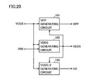
- FIG. 20 is a block diagram for describing an effect of the third embodiment
- FIG. 21 is a circuit diagram showing a configuration of a conventional internal power supply potential generating circuit
- FIG. 22 is a graph showing an operation of the internal power supply potential generating circuit shown in FIG. 21.
- FIG. 23 is a view for describing a problematic point of a conventional internal power supply potential generating circuit.
- FIG. 1 is a circuit diagram showing a configuration of an internal power supply potential generating circuit according to a first embodiment of the present invention.
- the internal power supply potential generating circuit includes: a potential dividing circuit 1 , a VCC1 generating circuit, a monitor potential generating circuit 3 ; a control potential generating circuit 4 ; and a drive circuit 5 .
- Potential dividing circuit 1 includes: N-channel MOS transistors 21 and 22 connected in series between a line at external power supply potential VCC0 and a line at ground potential GND.
- the gate of an N-channel MOS transistor 21 receives reference potential VR0.
- the gate of an N-channel MOS transistor 22 is connected to the drain thereof.
- the N-channel MOS transistor 22 constitutes a diode element.
- N-channel MOS transistors 21 and 22 are of the same transistor sizes (a channel width W and a channel length L) as each other.
- a potential VR1 VR0/2 1/2 times reference potential VR0 appears at a node between N-channel MOS transistors 21 and 22 .
- VCC1 generating circuit 2 includes: P-channel MOS transistors 11 to 13 ; N-channel MOS transistors 23 to 25 ; and a capacitor 33 .
- P-channel MOS transistors 11 and 12 are connected between the line at external power supply potential VCC0 and a node N 11 , and between the line at external power supply potential VCC0 and a node N 12 , respectively and the gates of both are connected to node N 12 .
- P-channel MOS transistors 11 and 12 constitute a current mirror circuit.
- N-channel MOS transistors 23 and 24 are connected between node N 11 and node N 25 , and between node N 12 and node N 25 , respectively and the gates of both receives reference a voltage VR1 and a monitor potential VM, respectively.
- a ratio W11/W12 of transistor sizes (ratio of channel widths) of P-channel MOS transistors 11 and 12 is equal to a ratio W23/W24 of transistor sizes of N-channel MOS transistors 23 and 24 .
- N-channel MOS transistor 25 is connected between node N 15 and the line at ground potential GND and the gate thereof receives a fixed potential VF.
- N-channel MOS transistor 25 constitutes a constant current source.
- MOS transistors 11 to 25 constitute a differential amplifier.
- P-channel MOS transistor 13 is connected between the line at external power supply potential VCC0 and node N 13 and the gate thereof is connected to node N 11 .
- Capacitor 33 is connected between node N 13 and the line at ground potential GND.
- N-channel MOS transistor 24 and P-channel MOS transistor 12 are connected in series with each other and P-channel MOS transistors 11 and 12 constitute a current mirror circuit, a current corresponding to monitor potential VM flows in P-channel MOS transistor 11 .
- monitor potential VM is higher than reference potential VR1
- a current flowing in P-channel MOS transistor 11 is larger than a current flowing in N-channel MOS transistor 23 to thereby cause node N 11 to have H level and to cause P-channel MOS transistor 13 to be non-conductive.
- monitor potential VM When monitor potential VM is lower than reference potential VR1, a current flowing in P-channel MOS transistor 11 is smaller than a current flowing in N-channel MOS transistor 23 to thereby cause node N 11 to have L level, to cause P-channel MOS transistor 13 to be conductive and to charge node N 13 .
- a potential at node N 13 becomes output potential VCC1 of VCC1 generating circuit 2 .
- Control potential generating circuit 4 includes: a P-channel MOS transistor 16 , an N-channel MOS transistor 28 , a P-channel MOS transistor 17 and an N-channel MOS transistor 29 , connected in series between output node N 13 of VCC1 generating circuit 2 and the line of ground potential GND.
- the gates of MOS transistors 16 and 29 receive internal power supply potential VO.
- the gate of N-channel MOS transistor 28 is connected to the drain thereof and the gate of P-channel MOS transistor 17 is connected to the drain thereof.
- MOS transistors 27 and 18 constitute respective diode elements. Control potential VC appears at node N 28 between MOS transistors 28 and 17 .
- Drive circuit 5 includes: P-channel MOS transistors 18 to 20 ; and N-channel MOS transistors 30 to 32 .
- P-channel MOS transistors 18 and 19 are connected between the line of external power supply potential VCC0 and node N 18 and between the line of external power supply potential VCC0 and node N 19 . The gates of both are connected to node N 18 .
- P-channel MOS transistors 18 and 19 constitute a current mirror circuit. A potential appearing at node N 19 becomes internal power supply potential VO.
- N-channel MOS transistor 30 is connected between nodes N 18 and N 19 and the gate thereof is connected to the gate of N-channel MOS transistor 28 .
- P-channel MOS transistor 20 is connected between nodes N 19 and N 20 and the gate thereof is connected to the gate of P-channel MOS transistor 17 .
- N-channel MOS transistors 31 and 32 are connected between node N 20 and the line at ground potential GND and between node N 19 and the line at ground potential GND and the gates of both are connected to node N 20 .
- N-channel MOS transistors 31 and 32 constitute a current mirror circuit.
- a ratio W28/W30 between transistor sizes of N-channel MOS transistors 28 and 30 is equal to a ratio W17/W20 between transistor sizes of P-channel MOS transistors 17 and 20 .
- a ratio W18/W19 between transistor sizes of P-channel MOS transistors 18 and 19 is equal to a ratio W31/W32 between transistor sizes of N-channel MOS transistors 31 and 32 .
- P-channel MOS transistors 18 and 19 cause a current W19/W18 times a current flowing in N-channel MOS transistor 30 to flow into node N 19 .
- P-channel MOS transistors 31 and 32 cause a current W32/W31 times a current flowing in P-channel MOS transistor 20 to flow out from node N 19 .
- N-channel MOS transistor 30 set to a value higher than that of N-channel MOS transistor 28 in order that no through current flows into the line at ground potential GND from the line at external power supply potential VCC0 through MOS transistors 18 , 30 , 20 and 31 , but a threshold voltage of MOS transistor 20 is set to a value higher than that of P-channel MOS transistor 17 .
- MOS transistors 30 and 20 are both become non-conductive.
- Monitor potential generating circuit 3 is a replica circuit of control potential generating circuit 4 and includes: P-channel MOS transistor 14 , N-channel MOS transistor 26 , P-channel MOS transistor 15 and N-channel MOS transistor 27 , connected in series between node N 13 and the line of ground potential GND.
- the gates of MOS transistors 14 and 27 are connected to node N 26 between MOS transistors 26 and 15 .
- a potential appeared at node N 26 becomes monitor potential VM.
- the gate of N-channel MOS transistor 26 is connected to the drain thereof and the gate of P-channel MOS transistor 15 is connected to the drain thereof.
- a configuration may be adopted that as shown in FIG. 2, potential dividing circuit 1 and VCC1 generating circuit 2 are replaced with a reference potential generating circuit 34 and an operational amplifier 35 , respectively.
- a non-inverting input terminal of operational amplifier 35 receives reference potential VR1, an inverting input terminal thereof receives monitor potential VM and an output terminal thereof is connected to the sources of P-channel MOS transistors 14 and 16 .
- FIG. 3 a configuration may be adopted in which reference potential generating circuit 34 is removed and drive circuit 5 is replaced with a drive circuit 36 .
- Drive circuit 36 is configured in a way that P-channel MOS transistors 18 and 19 , and N-channel MOS transistors 31 and 32 of drive circuit 5 are removed and the sources of MOS transistors 30 and 20 are connected to the line of external power supply potential VCC0 and the line of ground potential GND, respectively.
- VO VR0. Since MOS transistors 18 , 19 , 31 and 32 are removed, a layout area is favorably smaller though a current drive ability of internal power supply potential is reduced.
- FIG. 4 is a circuit diagram showing a configuration of an internal power supply potential generating circuit according to the second embodiment of the present invention.
- the internal power supply potential generating circuit includes: a lower limit potential comparison circuit 41 ; an upper limit potential comparison circuit 42 ; inverters 43 and 44 ; a P-channel MOS transistor 54 ; and an N-channel MOS transistor 64 .
- Lower limit potential comparison circuit 41 includes: P-channel MOS transistors 45 and 46 ; and N-channel MOS transistors 55 to 57 .
- P-channel MOS transistors 45 and 46 are connected between a line at external power supply potential VCC0 and a node N 45 , and between the line of external power supply potential VCC0 and a node N 46 , respectively, and the gates of both are connected to node N 45 .
- P-channel MOS transistors 45 and 46 constitute a current mirror circuit.
- N-channel MOS transistors 55 and 56 are connected between a node N 45 and a node N 57 , and between a node N 46 and node N 57 , respectively, and the gates of both receive reference potential VR0 and internal power supply potential VO, respectively.
- N-channel MOS transistor 57 is connected between node 57 and a line at ground potential GND and the gate thereof receives fixed potential VF0.
- N-channel MOS transistor 57 constitutes a constant current source.
- MOS transistors 45 , 46 and 55 to 57 constitute a differential amplifier. A signal appearing at node N 46 becomes output signal VC 1 of lower limit potential comparison circuit 41 .
- a ratio W45/W46 between transistor sizes of P-channel MOS transistors 45 and 46 is larger than a ratio W55/W56 between transistor sizes of N-channel MOS transistors 55 and 56 .
- Upper limit potential comparison circuit 42 includes: P-channel MOS transistors 47 to 49 ; and N-channel MOS transistors 58 and 59 .
- P-channel MOS transistor 47 is connected between the line of external power supply potential VCC0 and a node N 47 and the gate thereof receives fixed potential VF1.
- P-channel MOS transistor 47 constitutes a constant current source.
- P-channel MOS transistors 48 and 49 are connected between node N 47 and node N 48 , and between node N 47 and node N 49 , respectively, and the gates of both receive reference potential VR0 and internal power supply potential VO, respectively.
- N-channel MOS transistors 58 and 59 are connected between node N 48 and the line of ground potential GND, and between node N 49 and the line of ground potential GND and the gates of both are connected to node N 48 .
- N-channel MOS transistors 58 and 59 constitute a current mirror circuit.
- MOS transistors 47 to 49 , 58 and 59 constitute a differential amplifier. A signal appearing at node N 49 becomes an output signal VC 2 of upper limit potential comparison circuit 42 .
- a ratio W48/W49 between transistor sizes of P-channel MOS transistors 48 and 49 is smaller than a ratio W58/W59 between transistor sizes of N-channel MOS transistors 58 and 59 .
- Inverter 43 includes: P-channel MOS transistor 50 and N-channel MOS transistors 60 to 62 , connected in series between the line of external power supply potential VCC0 and the line of ground potential GND.
- the gates of MOS transistors 50 and 60 receive output signal VC 1 of lower limit potential comparison circuit 41 .
- the gate of N-channel MOS transistor 61 is connected to the drain thereof N-channel MOS transistor 61 constitutes a diode element.
- N-channel MOS transistor 61 is provided in order to set a threshold voltage of inverter 43 at an intermediate level of a potential variation width of signal VC 1 and to prevent a through current from flowing into the line of ground potential GND from the line of external power supply potential VCC0 through MOS transistors 50 and 60 to 62 .
- N-channel MOS transistor 62 receives fixed potential VF0.
- N-channel MOS transistor 62 constitutes a current limiting element to prevent MOS transistors 54 and 64 from becoming simultaneously conductive.
- a signal appearing at a node between MOS transistors 50 and 60 becomes an output signal VC 3 of inverter 43 .
- Inverter 44 includes: P-channel MOS transistors 51 to 53 ; and N-channel MOS transistor 63 , connected in series between the line of external power supply potential VCC0 and the line of ground potential GND.
- the gate of P-channel MOS transistor 51 receives fixed potential VF1.
- P-channel MOS transistor 51 constitutes a current limiting element to prevent MOS transistors 54 and 64 from becoming simultaneously conductive.
- the gate of P-channel MOS transistor 52 is connected to the drain thereof.
- P-channel MOS transistor 52 constitutes a diode element.
- P-channel MOS transistor 52 is provided in order to set a threshold voltage of inverter 44 to an intermediate level of a potential variation width of signal VC 2 and to prevent a through current from flowing into the line of ground potential GND from the line of external power supply potential VCC0 through MOS transistors 51 to 53 and 63 .
- the gates of MOS transistors 53 and 63 receive output signal VC 2 of upper limit potential comparison circuit 42 .
- a signal appearing at a node between MOS transistors 53 and 63 becomes an output signal VC 4 of inverter 44 .
- P-channel MOS transistor 54 is connected between the line of external power supply potential VCC0 and an output node N 54 and the gate thereof receives output signal VC 3 of inverter 43 .
- P-channel MOS transistor 54 constitutes a pull-up driver.
- N-channel MOS transistor 64 is connected between output node N 54 and the line of ground potential GND and the gate thereof receives output signal VC 4 of inverter 44 .
- a potential of output node N 54 becomes internal power supply potential VO.
- output signal VC 1 of lower limit potential comparison circuit 41 takes H level and output signal VC 3 of inverter 43 takes L level to thereby cause P-channel MOS transistor 54 to be conductive, and a current flows into node N 54 from the line of external power supply potential VCC0 through P-channel MOS transistor 54 to raise internal power supply potential VO.
- an output signal of upper limit potential comparison circuit 42 is kept unchanged at H level as is to hold P-channel MOS transistor 64 in a non-conductive state.
- output signal VC 2 of upper limit potential comparison circuit 42 takes H level and output signal VC 4 of inverter 44 takes H level to thereby cause N-channel MOS transistor 64 to be conductive, and a current flows into the line of ground potential GND from node N 54 to lower internal power supply potential VO.
- output signal VC 1 of lower limit potential comparison circuit 41 takes L level and output signal VC 3 of inverter 43 takes H level to thereby cause P-channel MOS transistor 54 to be non-conductive.
- a dead band can be set with ease and correctness since ratios W45/W46 and W55/W56 between transistor sizes in lower limit potential comparison circuit 41 are adjusted to set lower limit value VL and ratios W48/W49 and W58/W59 between transistor sizes in upper limit potential comparison circuit 42 are adjusted to set upper limit value VH.
- Potential dividing circuit 65 includes: N-channel MOS transistors 66 and 67 connected in series between the line of external power supply potential VCC0 and the line of ground potential GND.
- the gate of N-channel MOS transistor 66 receives reference potential VR0.
- the gate of N-channel MOS transistor 67 is connected to the drain thereof.
- Potential VR1 VR0/2 1/2 times reference potential VR0 appears at a node between N-channel MOS transistors 66 and 67 .
- Reference potential VR1 is given to lower limit potential comparison circuit 41 and upper limit potential comparison circuit 42 instead of reference potential VR0.
- Internal power supply potential generating circuit 68 is of the same configuration as the internal power supply potential generating circuit shown in FIG. 3 and generates internal power supply potential VO on the basis of reference potential VR1.
- Internal power supply potential generating circuit 69 is of the same configuration as the internal power supply potential generating circuit shown in FIG. 4 and generates internal power supply potential VO on the basis of reference potential VR1.
- Internal power supply potential generating circuits 68 and 69 are connected in parallel to each other.
- Internal power supply potential generating circuit 68 has a comparatively large width of a dead band A1, while having a large current drive ability even when output potential VO shifts largely from reference potential VR1.
- Internal power supply potential generating circuit 69 has a narrow width of a dead band B1 set with correctness, while having a small current drive ability when output potential VO shifts from reference potential VR1.
- Internal power supply potential generating circuit shown in FIG. 6 has a characteristic of a combination of characteristics of internal power supply potential generating circuits 68 and 69 and as shown by a curve C of FIG.
- a modification example of FIG. 8 is of a configuration obtained in a way that lower limit potential comparison circuit 41 and upper limit potential comparison circuit 42 of the internal power supply potential generating circuit of FIG. 4 are replaced with lower limit potential comparison circuit 41 ′ and upper limit potential comparison circuit 42 ′, respectively, and inverters 43 and 44 are removed therefrom.
- the gates of MOS transistors 55 and 56 receive output potential VO and reference potential VR0, respectively, and signal VC 1 is given directly to the gate of P-channel MOS transistor 54 .
- a ratio W45/W46 between transistor sizes of P-channel MOS transistors 45 and 46 is set to a value smaller than a ratio W55/W56 between transistor sizes of N-channel MOS transistors 55 and 56 .
- MOS transistors 48 and 49 receive output potential VO and reference potential VR0, respectively, and signal VC 2 is given directly to the gate of N-channel MOS transistor 64 .
- a ratio W48/W49 between transistor sizes of P-channel MOS transistors 48 and 49 is set to a value larger than a ratio W58/W59 between transistor sizes of N-channel MOS transistors 58 and 59 .
- a modification example of FIG. 9 is of a configuration obtained in a way that upper limit potential comparison circuit 42 , inverter 44 and N-channel MOS transistor 64 are removed from the internal power supply potential generating circuit of FIG. 4. This can be used in a case where a current flows out into the line of ground potential GND from output node N 54 through a load circuit (not shown) at all times. In this case, a layout area becomes smaller by a value corresponding to upper potential comparison circuit 42 , inverter 44 and N-channel MOS transistor 64 . Note that transistor sizes of N-channel MOS transistors 55 and 56 may the same as each other.
- FIG. 11 A modification example of FIG. 11 is of a configuration obtained in a way that inverters 43 and 44 in the internal power supply potential circuit of FIG. 4 are replaced with inverters 71 and 72 .
- Inverter 71 is constructed in a way that in inverter 43 , N-channel MOS transistor 61 is removed and the source of N-channel MOS transistor 60 is connected to the drain of N-channel MOS transistor 62 .
- Inverter 72 is constructed in a way that in inverter 44 , N-channel MOS transistor 52 is removed and the drain of P-channel MOS transistor 51 is connected to the source of P-channel MOS transistor 53 .
- a modification example of FIG. 12 is of a configuration obtained in a way that a P-channel MOS transistor 73 is added to the internal power supply potential generating circuit of FIG. 11.
- P-channel MOS transistor 73 is connected between the drain of P-channel MOS transistor 54 and output node N 54 and the gate thereof receives output signal VC 4 of inverter 72 .
- signal VC 4 is at L level, not only does P-channel MOS transistor 73 becomes conductive, but N-channel MOS transistor 64 also becomes non-conductive, while when signal VC 4 is at H level, not only does N-channel MOS transistor 73 become non-conductive, but N-channel MOS transistor 64 also becomes conductive.
- a through current can be prevented from flowing into the line of ground potential GND from the line of external power supply potential VCC0 through MOS transistors 54 , 73 and 64 .
- a modification example of FIG. 13 is of a configuration obtained in a way that an OR gate 74 is added to the internal power supply potential circuit of FIG. 11.
- OR gate 74 receives output signals VC 3 and VC 4 of inverters 71 and 72 and output signal thereof is given to the gate of P-channel MOS transistor 54 .
- P-channel MOS transistor 54 becomes non-conductive.
- a through current can be prevented from flowing into the line of ground potential GND from the line of external power supply potential VCC0 through MOS transistors 54 , 73 and 64 .
- a modification example of FIG. 14 is of a configuration obtained in a way that a step-down circuit (VDC) 75 is added to the internal power supply potential generating circuit of FIG. 4.
- Step-down circuit 75 lowers external power supply potential VCC0 to generate internal power supply potential VCCS and to give internal power supply potential VCCS to the source of P-channel MOS transistor 54 .
- a current drive ability of step-down circuit 75 becomes smaller when output signal VC 3 of inverter 43 is at H level, while becoming larger when signal VC 3 is at L level. That is, step-down circuit 75 , as shown in FIG. 15, includes: operational amplifiers 80 and 81 ; an inverter 82 ; an N-channel MOS transistor 83 ; P-channel MOS transistors 84 to 86 ; and a capacitor 87 .
- P-channel MOS transistors 85 and 86 are connected in parallel between the line of external power supply potential VCC0 and the source (a node N 85 ) of P-channel MOS transistor 54 .
- a transistor size of P-channel MOS transistor 85 is larger than that of P-channel MOS transistor 86 .
- the non-converting input terminal of operational amplifier 81 receives reference potential VRS, the inverting input terminal thereof is connected to node N 85 and the output terminal thereof is connected to the gate of P-channel MOS transistor 86 .
- Operational amplifier 81 controls a gate potential of P-channel MOS transistor 86 in order that a potential at node N 85 coincides with reference potential VRS.
- Operational amplifier 80 receives reference potential VRS at the non-inverting input terminal thereof, the inverting input terminal thereof is connected to node N 85 and an output signal thereof is inputted to the gate of P-channel MOS transistor 85 .
- N-channel MOS transistor 83 is connected between the ground node of operational amplifier 83 and the line of ground potential GND and P-channel MOS transistor 84 is connected between the line of external power supply potential VCC0 and the gate of P-channel MOS transistor 85 .
- Output signal VC 3 of inverter 43 is inputted to the gates of MOS transistors 83 and 84 through inverter 82 .
- Capacitor 87 is connected between node N 85 and the line of ground potential GND to stabilize potential VCCS at node N 85 .
- N-channel MOS transistor 83 When signal VC 3 is at H level, N-channel MOS transistor 83 becomes non-conductive, not only is operational amplifier 80 deactivated, but P-channel MOS transistor 84 also becomes conductive, the gate of P-channel MOS transistor 85 is fixed at H level and P-channel MOS transistor 85 becomes non-conductive to decrease a current drive ability of step-down circuit 75 .
- signal VC 3 is at L level, N-channel MOS transistor 83 becomes conductive, not only is operational amplifier 80 activated but P-channel MOS transistor 84 also becomes non-conductive, and operational amplifier 80 controls a gate potential of P-channel MOS transistor 84 in order that a potential at node N 85 coincides with reference potential VRS to increase a current drive ability of step-down circuit 75 .
- step-down circuit 75 since a current drive ability of step-down circuit 75 increases only when P-channel MOS transistor 54 is caused to be conductive, while when P-channel MOS transistor 54 is caused to be nonconductive, a current drive ability of step-down circuit 75 decreases, a smaller power consumption of step-down circuit 75 is realized.
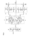
- FIG. 16 is a circuit block diagram showing an overall configuration of a DRAM according to a third embodiment of the present invention.
- the DRAM includes: an internal power supply potential generating circuit 91 , a clock generating circuit 92 ; a row/column address buffer 93 ; a row decoder 94 ; a column decoder 95 ; a memory mat 96 ; an input buffer 99 and an output buffer 100 , wherein memory mat 96 includes: a memory array 97 and a sense amplifier+input/output control circuit 98 .
- Internal power supply potential generating circuit 91 generates internal power supply potentials VPP, VDDS and VO on the basis of power supply potential VCC0, ground potential GND and reference potential VR0, given externally to supply over the entire DRAM. That is, internal power supply potential generating circuit 91 , as described in FIG. 17, includes: a VPP generating circuit 101 , a VDDS generating circuit 102 and a VR0/2 generating circuit 103 .
- VPP generating circuit 10 generates internal power supply potential VPP used as a select level for a word line WL on the basis of external power supply potential VCC0 and internal power supply potential VDDS. Internal power supply potential VPP is maintained at VDDS+2Vthn.
- VDDS generating circuit 102 generates internal power supply potential VDDS for a sense amplifier 112 on the basis of external power supply potential VCC0 and reference potential VR0. Internal power supply potential VDDS is maintained at VR0.
- VR0/2 generating circuit 103 is of the same configuration as the internal power supply potential generating circuit shown in FIG. 6 and generates internal power supply potential VO used as a bit line precharge potential VBL and a cell plate potential VCP on the basis of external power supply potential VCC0 and reference potential VR0. Internal power supply potential VO is maintained at VR0/2.
- Clock generating circuit 92 selects a prescribed operating mode according to external control signals /RAS and /CAS to control the entire DRAM.
- Row/column address buffer 93 generates row address signals RA to RAi and column address signals CA 0 to CAi according to external address signals A 0 to Ai (where i is an integer of 0 or more) to give thus generated signals RA to RAi and CA 0 to CAi to row decoder 94 and column decoder 95 , respectively.
- Memory array 97 includes: plural memory cells each storing 1 bit data.
- the memory cells are each placed at a site with a prescribed address to be composed of a row address and a column address.
- Row decoder 94 designates a row address of memory array 97 according to row address signal RA 0 to RAi given from row/column address buffer 93 .
- Column decoder 95 designates a column address of memory array 97 according to column address signal CA 0 to CAi given from tow/column address buffer 93 .
- Sense amplifier+input/output control circuit 98 connects a memory cell at an address designated by row decoder 94 and column decoder 95 to one end of a data input/output line pair IOP.
- the other end of data input/output line pair IOP is connected to input buffer 99 and output buffer 100 .
- Input buffer 99 in write mode, responds to an external control signal /W to give a data signal Dj (where j is an integer of 0 or more) inputted externally to a selected memory cell through data input/output line pair IOP.
- Output buffer 100 in read mode, responds to an external control signal /OE to output a read data signal Qj from a selected memory cell to outside.
- FIG. 18 is a circuit block diagram showing configurations of DRAM memory array 97 and sense amplifier+input/output control circuit 98 combined shown in FIG. 17 and
- FIG. 19 is a circuit diagram showing a more detailed configuration of one column in memory array 97 and sense amplifier+input/output control circuit 98 shown in FIG. 18.
- memory array 97 includes: plural memory cells MC arranged in a matrix; word lines WL provided correspondingly to respective rows; and bit line pair BL and /BL provided correspondingly to respective columns.
- Each memory cell MC includes: an N-channel MOS transistor 132 for access; and a capacitor 133 for information storage.
- the gate of N-channel MOS transistor 132 of each memory cell MC is connected to a word line WL on a corresponding row.
- N-channel MOS transistor 132 is connected between bit line BL or /BL on a corresponding column and one electrode (storage node SN) of capacitor 133 of memory cell MC.
- the other electrode of capacitor 133 of each memory cell MC receives cell plate potential VCP.
- One end of each word line WL is connected to row decoder 94 .
- Sense amplifier+input/output control circuit 98 includes: column select lines CSL, column select gates 111 , sense amplifiers 112 and equalizers 113 provided correspondingly to respective columns; a driver 114 and a data input/output line pair IO and /IO (IOP).
- Column select gate 111 includes: N-channel MOS transistors 121 and 122 connected between bit lines BL and /BL, respectively, of a corresponding pair and between data input/output lines IO and /IO. The gates of N-channel MOS transistors 121 and 122 are connected to column decoder 95 through corresponding column select line CSL.
- N-channel MOS transistors 121 and 122 becomes conductive to couple bit lines BL and /BL to data input/output line pair IO and /IO.
- Sense amplifier 112 includes: N-channel MOS transistors 123 and 124 connected between bit lines BL and a node N 112 , and between bit line /BL and node N 112 , respectively; and P-channel MOS transistors 125 and 126 connected between bit line BL and a node 112 ′, and between bit line /BL and node N 112 ′, respectively.
- the gates of MOS transistors 123 and 125 are both connected to bit line /BL and the gates of MOS transistors 124 and 126 are both connected to bit line BL.
- Driver 114 includes: an N-channel MOS transistor 127 connected between node 112 and the line of ground potential GND and a P-channel MOS transistor 128 connected between node N 112 ′ and the line of internal power supply potential VDDS.
- MOS transistors 127 and 128 receive sense amplifier activation signals SE and /SE at the respective gates thereof. When sense amplifier activation signals SE and /SE take H level and L level, respectively, MOS transistors 127 and 128 become conductive, nodes N 112 and N' 112 take ground potential GND and internal power supply potential VDDS, respectively, and sense amplifier 112 amplifies a small potential difference between bit lines BL and /BL to internal power supply potential VDDS.
- Equalizer 113 includes: an N-channel MOS transistor 129 connected between bit lines BL and /BL; and an N-channel MOS transistors 130 and 131 connected between bit line BL and a node N 113 ′, and between bit line /BL and node N 113 ′, respectively.
- the gates of N-channel MOS transistors 129 to 131 are all connected to a node N 113 .
- Equalizer 113 equalizes potentials on bit lines BL and /BL to bit line precharge potential VBL in response to a rise of bit line equalize signal BLEQ to H level at activation level.
- Input buffer 99 responds to signal /W to give write data signal Dj given externally to bit lines BL and /BL on a selected column through data input/output line pair IOP.
- Write data signal Dj is given as a potential difference between bit lines BL and /BL.
- a word line WL on a row corresponding to a row address signal RA 0 to RAi is raised to H level at select level (internal power supply potential VPP) to cause MOS transistor 132 of memory cell MC on the row to be conductive.
- An electric charge corresponding to potentials on bit lines BL or /BL is stored in capacitor 133 of selected memory cell MC.
- bit line equalize signal BLEQ is at first lowered to L level to cause N-channel MOS transistors 129 to 131 of equalizer 113 to be non-conductive and to thereby cease equalization on bit lines BL and /BL. Then, a word line WL on a row corresponding to row address signal RA 0 to RAi is raised to H level at select level by row decoder 94 . In response to this, a potential on BL and /BL alter by a small amount according to an electric charge in capacitor 133 of activated memory cell MC.
- sense amplifier activation signal SE and /SE take H level and L level, respectively, to activate sense amplifier 112 .
- resistance values of MOS transistors 124 and 125 are smaller than those of MOS transistors 123 and 126 to not only raise a potential on bit line BL to H level (internal power supply potential VDSS) but also lower a potential on bit line /BL to L level (ground potential GND).
- resistance values of MOS transistors 123 and 126 are smaller than those of MOS transistors 124 and 125 to not-only raise a potential on bit line /BL to H level (internal power supply potential VDSS) but also lower a potential on bit line BL to L level (ground potential GND).
- column select line CSL on a column corresponding to column address signal CA 0 to CAi is raised to H level at select level by column decoder 95 to cause column select gate 111 of the column to be conductive.
- Data on bit lines BL and /Bl on a selected column is given to output buffer 10 through column select gate 111 and data input/output line pair IO and /IO.
- Output buffer 100 responds to signal /OE to output read data signal Qj to outside.
- bit line precharge potential VBL and cell plate potential VCP can be controlled to VR0/2 with correctness.
- VDDS generating circuit 150 which was an intermediate potential generating circuit. Therefore, as described in the section of description of the background art, it has been difficult to adjust VO to VR0/2 so as to coincide with each other. According to the third embodiment, however, VO can be adjusted so as to correctly coincide with VR/2, thereby enabling correct reading of a data signal.
Abstract
Description
- 1. Field of the Invention
- The present invention relates to a potential generating circuit, and particularly to a potential generating circuit charging and discharging an output node in order that a potential of the output node becomes a potential corresponding to a reference potential.
- 2. Description of the Background Art
- With the purpose to reduce power consumption, there has been heretofore provided an internal power supply potential generating circuit for generating an internal power supply potential VO lower than an external power supply potential VCC0 in a semiconductor integrated circuit device.
- FIG. 21 is a circuit diagram showing a configuration of such an internal power supply potential generating circuit. In FIG. 21, the internal power supply potential generating circuit includes: an
operational amplifier 151; P-channel MOS transistors 152 to 154; and N-channel MOS transistors 155 to 157.Operational amplifier 151 constitutes a voltage follower and outputs a current so as to cause a potential VDDS at a node N151 to coincide with a reference potential VR0.MOS transistors MOS transistors channel MOS transistors channel MOS transistor 155, and the gates of P-channel MOS transistors channel MOS transistor 153. The gates ofMOS transistors MOS transistors - Transistor parameters of
MOS transistors MOS transistors channel MOS transistor 157 set to a value higher than that of N-channel MOS transistor 155, but a threshold voltage of P-channel MOS transistor 154 is also set to a value higher than that of P-channel MOS transistor 153 in order that no through current flows into the line at ground potential GND from the line at external power supply potential VCC0 throughMOS transistors MOS transistors - FIG. 22 is a graph showing an operation of the internal power supply potential generating circuit shown in FIG. 21. In FIG. 22, a straight line E in FIG. 22 shows a relationship between output potential VO and a drive current I of the internal power supply potential generating circuit.
MOS transistors channel MOS transistor 152 becomes higher, but a resistance value of N-channel MOS transistor 156 also becomes lower to lower gate potentials ofMOS transistors channel MOS transistor 154 to be conductive, to thereby cause a discharge current to flow and to lower internal power supply potential VO. With internal power supply potential VO lower than lower limit value VL, not only a resistance value of P-channel MOS transistor 152 become lower, but a resistance value of N-channel MOS transistor 96 also becomes higher, to raise gate potentials ofMOS transistors channel MOS transistor 157 to be conductive, to thereby cause a charge current flow and to raise internal power supply potential VO. Therefore, internal power supply potential VO is held at a potential between lower limit value VL and upper limit value VH. - In such an internal power supply potential generating circuit, a necessity arises for setting a source-to-drain voltage Vsdp of P-
channel MOS transistor 152, a threshold voltage Vthn of N-channel MOS transistor 155, a threshold voltage Vthp of P-channel MOS transistor 153 and a drain-to-source voltage Vdsn of N-channel MOS transistor 156 in order that VC=VDDS/2=VR0/2 when VO=VC. - With lower VDDS, miniaturized layout, constraint from other circuits, fluctuations in fabrication parameters and others, more of difficulty has become a reality in fabrication of MOS transistors in matching Vsdp, Vthn, Vthp and Vdsn with design values. A result ends up with generation of an error voltage ΔV between internal power supply potential VO and a target potential VR0/2 as shown in FIG. 23 without matching Vsdp, Vthn, Vthp and Vdsn with design values.
- In a conventional internal power supply potential generating circuit, not only were threshold voltages of N-
channel MOS transistors channel MOS transistors - It is, therefore, a main object of the present invention to provide a potential generating circuit capable of correctly controlling a potential at an output node.
- It is another object of the present invention to provide a potential generating circuit capable of correctly controlling a dead band width.
- A potential generating circuit according to the present invention, as described above, includes: a first transistor of a first conductive type, a first electrode of which is connected to a line at a first power supply potential, and a second electrode of which is connected to a output node; a second transistor of a second conductive type, a first electrode of which is connected to a line at a second power supply potential, and a second electrode of which is connected to the output node; a control potential generating circuit; a monitor potential generating circuit; and a current supply circuit. The control potential generating circuit includes: a third transistor of the second conductive type, a first electrode of which is connected to a first node, an input electrode of which is connected to the output node, and a second electrode of which is connected to an input electrode of the first transistor; a fourth transistor of the first conductive type, a first electrode of which is connected to the line at the second power supply potential, an input electrode of which is connected to the output node, and a second electrode of which is connected to an input electrode of the second transistor; and first and second diode elements connected in series between the second electrodes of the third and fourth transistors, wherein the first and second transistors are controlled in order that a potential at the output node coincides with a potential at a second node between the first and second diode elements. The monitor potential generating circuit includes: a fifth transistor of the second conductive type, a first electrode of which is connected to the first node and an input electrode of which is connected to a third node; a sixth transistor of the first conductive type, a first electrode of which is connected to the line at the second power supply potential, and an input electrode of which is connected to the third node; a third diode element connected between a second electrode of the fifth transistor and the third node; and a fourth diode element connected between the third node and a second electrode of the sixth transistor, wherein a monitor potential is outputted from the third node. The current supply circuit supplies a current to the first node in order that the monitor potential coincides with the reference potential. Therefore, when the monitor potential coincides with the reference potential, a potential at the second node takes the reference potential and a potential at the output node also further takes the reference potential. Accordingly, a potential at the output node can be caused to correctly coincide with the reference potential.
- In another potential generating circuit according to the present invention, there are provided: a first comparison circuit; a second comparison circuit; and a drive circuit. The first comparison circuit includes: first and second transistors, input electrodes of which receive a reference potential and a potential at an output node, respectively, and outputs a first signal at a level corresponding to a potential difference between the potential at the output node and a lower limit potential lower than the reference potential by a first offset voltage. The second comparison circuit includes: third and fourth transistors, input electrodes of which receive the reference potential and the potential at the output node, respectively, and outputs a second signal at a level corresponding to a potential difference between the potential at the output node and an upper limit potential higher than the reference potential by a second offset voltage. The drive circuit operates in response to the first and second signals from the first and second comparison circuits, causing a current to flow into the output node when the potential at the output node is lower than the lower limit potential, while when the potential at the output node is higher than the lower limit potential, causing a current to flow out from the output node. Therefore, by setting a first offset voltage of the first comparison circuit, a lower limit potential can be set, and by setting a second offset voltage of the second comparison circuit, an upper limit potential can be set; and a dead band arises between the lower limit potential and the upper limit potential, thereby enabling setting of a width of the dead band with good precision.
- The foregoing and other objects, features, aspects and advantages of the present invention will become more apparent from the following detailed description of the present invention when taken in conjunction with the accompanying drawings.
- FIG. 1 is a circuit diagram showing a configuration of an internal power supply potential generating circuit according to a first embodiment of the present invention;
- FIG. 2 is a circuit block diagram showing a modification example of the first embodiment;
- FIG. 3 is a circuit diagram showing another modification example of the first embodiment;
- FIG. 4 is a circuit diagram showing a configuration of an internal power supply potential generating circuit according to a second embodiment of the present invention;
- FIG. 5 is a circuit diagram showing a modification example of the second embodiment;
- FIG. 6 is a block diagram showing another modification example of the second embodiment;
- FIGS. 7A and 7B are graphs showing operations of the internal power supply potential generating circuit shown in FIG. 6;
- FIG. 8 is a circuit diagram showing still another modification example of the second embodiment;
- FIG. 9 is a circuit diagram showing still another modification example of the second embodiment;
- FIG. 10 is a graph showing an operation of still another modification example of the second embodiment;
- FIG. 11 is a circuit diagram showing still another modification example of the second embodiment;
- FIG. 12 is a circuit diagram showing still another modification example of the second embodiment;
- FIG. 13 is a circuit diagram showing still another modification example of the second embodiment;
- FIG. 14 is a circuit diagram showing still another modification example of the second embodiment;
- FIG. 15 is a circuit diagram showing a configuration of a set-down circuit shown in FIG. 14;
- FIG. 16 is a circuit block diagram showing an overall configuration of a DRAM according to a third embodiment of the present invention;
- FIG. 17 is a block diagram showing a configuration of an internal power supply potential generating circuit shown in FIG. 16;
- FIG. 18 is a circuit block diagram showing a configuration of a memory mat shown in FIG. 16;
- FIG. 19 is a circuit diagram showing a more detailed configuration of the memory mat shown in FIG. 18;
- FIG. 20 is a block diagram for describing an effect of the third embodiment;
- FIG. 21 is a circuit diagram showing a configuration of a conventional internal power supply potential generating circuit;
- FIG. 22 is a graph showing an operation of the internal power supply potential generating circuit shown in FIG. 21; and
- FIG. 23 is a view for describing a problematic point of a conventional internal power supply potential generating circuit.
- First Embodiment
- FIG. 1 is a circuit diagram showing a configuration of an internal power supply potential generating circuit according to a first embodiment of the present invention. In FIG. 1, the internal power supply potential generating circuit includes: a
potential dividing circuit 1, a VCC1 generating circuit, a monitorpotential generating circuit 3; a controlpotential generating circuit 4; and adrive circuit 5. -
Potential dividing circuit 1 includes: N-channel MOS transistors channel MOS transistor 21 receives reference potential VR0. The gate of an N-channel MOS transistor 22 is connected to the drain thereof. The N-channel MOS transistor 22 constitutes a diode element. N-channel MOS transistors channel MOS transistors -
VCC1 generating circuit 2 includes: P-channel MOS transistors 11 to 13; N-channel MOS transistors 23 to 25; and acapacitor 33. P-channel MOS transistors channel MOS transistors channel MOS transistors - A ratio W11/W12 of transistor sizes (ratio of channel widths) of P-
channel MOS transistors channel MOS transistors channel MOS transistor 25 is connected between node N15 and the line at ground potential GND and the gate thereof receives a fixed potential VF. N-channel MOS transistor 25 constitutes a constant current source.MOS transistors 11 to 25 constitute a differential amplifier. P-channel MOS transistor 13 is connected between the line at external power supply potential VCC0 and node N13 and the gate thereof is connected to node N11.Capacitor 33 is connected between node N13 and the line at ground potential GND. - Since N-
channel MOS transistor 24 and P-channel MOS transistor 12 are connected in series with each other and P-channel MOS transistors channel MOS transistor 11. When monitor potential VM is higher than reference potential VR1, a current flowing in P-channel MOS transistor 11 is larger than a current flowing in N-channel MOS transistor 23 to thereby cause node N11 to have H level and to cause P-channel MOS transistor 13 to be non-conductive. When monitor potential VM is lower than reference potential VR1, a current flowing in P-channel MOS transistor 11 is smaller than a current flowing in N-channel MOS transistor 23 to thereby cause node N11 to have L level, to cause P-channel MOS transistor 13 to be conductive and to charge node N13. A potential at node N13 becomes output potential VCC1 ofVCC1 generating circuit 2. - Control
potential generating circuit 4 includes: a P-channel MOS transistor 16, an N-channel MOS transistor 28, a P-channel MOS transistor 17 and an N-channel MOS transistor 29, connected in series between output node N13 ofVCC1 generating circuit 2 and the line of ground potential GND. The gates ofMOS transistors channel MOS transistor 28 is connected to the drain thereof and the gate of P-channel MOS transistor 17 is connected to the drain thereof.MOS transistors MOS transistors MOS transistors potential generating circuit 4controls MOS transistors MOS transistors -
Drive circuit 5 includes: P-channel MOS transistors 18 to 20; and N-channel MOS transistors 30 to 32. P-channel MOS transistors channel MOS transistors channel MOS transistor 30 is connected between nodes N18 and N19 and the gate thereof is connected to the gate of N-channel MOS transistor 28. P-channel MOS transistor 20 is connected between nodes N19 and N20 and the gate thereof is connected to the gate of P-channel MOS transistor 17. N-channel MOS transistors channel MOS transistors - A ratio W28/W30 between transistor sizes of N-
channel MOS transistors channel MOS transistors channel MOS transistors channel MOS transistors channel MOS transistors channel MOS transistor 30 to flow into node N19. P-channel MOS transistors channel MOS transistor 20 to flow out from node N19. - Not only is a threshold voltage of N-
channel MOS transistor 30 set to a value higher than that of N-channel MOS transistor 28 in order that no through current flows into the line at ground potential GND from the line at external power supply potential VCC0 throughMOS transistors MOS transistor 20 is set to a value higher than that of P-channel MOS transistor 17. With such setting, when output potential VO resides in a dead band from lower limit value VL=VR0/2−ΔV1 to upper limit value VH=VR0/2+ΔV2,MOS transistors - When internal power supply potential VO becomes higher than upper limit value VH, not only does a resistance value of P-
channel MOS transistor 16 higher, but a resistance value of N-channel MOS transistor 29 also becomes lower to lower gate potentials ofMOS transistors channel MOS transistor 20 to be conductive and to lower internal power supply potential VO. - When internal power supply potential VO becomes lower than lower limit value VL, not only does a resistance value of P-
channel MOS transistor 16 become lower, but a resistance value of N-channel MOS transistor 29 also becomes higher to raise gate potentials ofMOS transistors channel MOS transistor 30 to be conductive and to raise internal power supply potential VO. Internal power supply potential VO is, therefore, held at a potential between lower limit value VL and upper limit value VH. - Monitor
potential generating circuit 3 is a replica circuit of controlpotential generating circuit 4 and includes: P-channel MOS transistor 14, N-channel MOS transistor 26, P-channel MOS transistor 15 and N-channel MOS transistor 27, connected in series between node N13 and the line of ground potential GND. The gates ofMOS transistors MOS transistors channel MOS transistor 26 is connected to the drain thereof and the gate of P-channel MOS transistor 15 is connected to the drain thereof. - A ratio W14/W16 between transistor sizes of P-
channel MOS transistors channel MOS transistors channel MOS transistors channel MOS transistors -
VCC1 generating circuit 2, as described above, controls VCC1 in order that VM=VC=VR0/2. Therefore, even if transistor parameters ofMOS transistors MOS transistors - A configuration may be adopted that as shown in FIG. 2,
potential dividing circuit 1 andVCC1 generating circuit 2 are replaced with a referencepotential generating circuit 34 and anoperational amplifier 35, respectively. Referencepotential generating circuit 34 generates reference potential VR1=VR0/K (where K is a positive real number) on the basis of reference voltage VR0. A non-inverting input terminal ofoperational amplifier 35 receives reference potential VR1, an inverting input terminal thereof receives monitor potential VM and an output terminal thereof is connected to the sources of P-channel MOS transistors Operational amplifier 35 controls VCC1 in order that monitor potential VM coincides with reference potential VR1. In this modification example, VO=VR1. - Furthermore, as shown in FIG. 3, a configuration may be adopted in which reference
potential generating circuit 34 is removed and drivecircuit 5 is replaced with adrive circuit 36. Drivecircuit 36 is configured in a way that P-channel MOS transistors channel MOS transistors drive circuit 5 are removed and the sources ofMOS transistors MOS transistors - Second Embodiment
- FIG. 4 is a circuit diagram showing a configuration of an internal power supply potential generating circuit according to the second embodiment of the present invention. In FIG. 4, the internal power supply potential generating circuit includes: a lower limit
potential comparison circuit 41; an upper limitpotential comparison circuit 42;inverters channel MOS transistor 54; and an N-channel MOS transistor 64. - Lower limit
potential comparison circuit 41 includes: P-channel MOS transistors channel MOS transistors 55 to 57. P-channel MOS transistors channel MOS transistors channel MOS transistors channel MOS transistor 57 is connected betweennode 57 and a line at ground potential GND and the gate thereof receives fixed potential VF0. N-channel MOS transistor 57 constitutes a constant current source.MOS transistors potential comparison circuit 41. - A ratio W45/W46 between transistor sizes of P-
channel MOS transistors channel MOS transistors MOS transistors MOS transistor 56 is larger than W45=W46=W55. In case where VO=VR0, therefore, a current I46 flowing in P-channel MOS transistor 46 becomes smaller than a current I56 flowing in N-channel MOS transistor 56, while when internal power supply potential VO becomes lower limit value VL=VR0−ΔV1, I46=I56. - When internal power supply potential VO is higher than lower limit value VL, therefore, current I46 flowing in P-
channel MOS transistor 46 becomes smaller than current I56 flowing in N-channel MOS transistor 56 to cause output signal VC1 to be at L level, while internal power supply potential VO is lower than lower limit value VL, I46 becomes larger than I56 to cause output signal VC1 to be at H level. - Upper limit
potential comparison circuit 42 includes: P-channel MOS transistors 47 to 49; and N-channel MOS transistors channel MOS transistor 47 is connected between the line of external power supply potential VCC0 and a node N47 and the gate thereof receives fixed potential VF1. P-channel MOS transistor 47 constitutes a constant current source. P-channel MOS transistors channel MOS transistors channel MOS transistors MOS transistors 47 to 49, 58 and 59 constitute a differential amplifier. A signal appearing at node N49 becomes an output signal VC2 of upper limitpotential comparison circuit 42. - A ratio W48/W49 between transistor sizes of P-
channel MOS transistors channel MOS transistors MOS transistors MOS transistor 49 is larger than channel widths W48=W58=W59. Therefore, when VO=VR0, a current I49 flowing in P-channel MOS transistor 49 becomes larger than a current I59 flowing in N-channel MOS transistor 59, while when VO becomes upper limit value VH=VR0+ΔV2, I49=I59. - When internal power supply potential VO is higher than upper limit value VH, therefore, current I49 flowing in P-
channel MOS transistor 49 becomes smaller than current I59 flowing in N-channel MOS transistor 59 to cause output signal VS2 to be at L level, while when VO is lower than upper limit value VH, I49 becomes larger than I59 to cause output signal VC2 to be at H level. -
Inverter 43 includes: P-channel MOS transistor 50 and N-channel MOS transistors 60 to 62, connected in series between the line of external power supply potential VCC0 and the line of ground potential GND. The gates ofMOS transistors potential comparison circuit 41. The gate of N-channel MOS transistor 61 is connected to the drain thereof N-channel MOS transistor 61 constitutes a diode element. N-channel MOS transistor 61 is provided in order to set a threshold voltage ofinverter 43 at an intermediate level of a potential variation width of signal VC1 and to prevent a through current from flowing into the line of ground potential GND from the line of external power supply potential VCC0 throughMOS transistors channel MOS transistor 62 receives fixed potential VF0. N-channel MOS transistor 62 constitutes a current limiting element to preventMOS transistors MOS transistors inverter 43. - When signal VC 1 is at L level, not only does P-
channel MOS transistor 50 become conductive, but N-channel MOS transistor 60 also becomes non-conductive to cause output signal VC3 to be at H level. When signal VC1 is at H level, not only does P-channel MOS transistor 50 become non-conductive, but N-channel MOS transistor 60 also becomes conductive to cause output signal VC3 to be at L level. -
Inverter 44 includes: P-channel MOS transistors 51 to 53; and N-channel MOS transistor 63, connected in series between the line of external power supply potential VCC0 and the line of ground potential GND. The gate of P-channel MOS transistor 51 receives fixed potential VF1. P-channel MOS transistor 51 constitutes a current limiting element to preventMOS transistors channel MOS transistor 52 is connected to the drain thereof. P-channel MOS transistor 52 constitutes a diode element. P-channel MOS transistor 52 is provided in order to set a threshold voltage ofinverter 44 to an intermediate level of a potential variation width of signal VC2 and to prevent a through current from flowing into the line of ground potential GND from the line of external power supply potential VCC0 throughMOS transistors 51 to 53 and 63. The gates ofMOS transistors potential comparison circuit 42. A signal appearing at a node betweenMOS transistors inverter 44. - When signal VC 2 is at L level, not only does P-
channel MOS transistor 53 become conductive, but N-channel MOS transistor 63 also becomes non-conductive to cause output signal VC4 to be at H level. When signal VC2 is at H level, not only does P-channel MOS transistor 53 become non-conductive, but N-channel MOS transistor 63 also becomes conductive to cause output signal VC4 to be at L level. - P-
channel MOS transistor 54 is connected between the line of external power supply potential VCC0 and an output node N54 and the gate thereof receives output signal VC3 ofinverter 43. P-channel MOS transistor 54 constitutes a pull-up driver. N-channel MOS transistor 64 is connected between output node N54 and the line of ground potential GND and the gate thereof receives output signal VC4 ofinverter 44. A potential of output node N54 becomes internal power supply potential VO. - Description will then be given of operation of the internal power supply potential generating circuit. When internal power supply potential VO is in a dead band between lower limit value VL=VR0−ΔV1 and upper limit value VH=VR0+ΔV2, output signal VC 1 of lower limit
potential comparison circuit 41 takes L level and output signal VC3 takes H level to thereby cause P-channel MOS transistor 54 to be non-conductive. Furthermore, output signal VC2 of upper limitpotential comparison circuit 42 takes H level and output signal VC4 takes L level to thereby cause N-channel MOS transistor 64 to be non-conductive. Therefore, output signal N54 enters a high impedance state. - When internal power supply potential VO becomes lower than lower limit value VL, output signal VC 1 of lower limit
potential comparison circuit 41 takes H level and output signal VC3 ofinverter 43 takes L level to thereby cause P-channel MOS transistor 54 to be conductive, and a current flows into node N54 from the line of external power supply potential VCC0 through P-channel MOS transistor 54 to raise internal power supply potential VO. At this time, an output signal of upper limitpotential comparison circuit 42 is kept unchanged at H level as is to hold P-channel MOS transistor 64 in a non-conductive state. - When internal power supply potential VO becomes higher than upper limit value VH, output signal VC 2 of upper limit
potential comparison circuit 42 takes H level and output signal VC4 ofinverter 44 takes H level to thereby cause N-channel MOS transistor 64 to be conductive, and a current flows into the line of ground potential GND from node N54 to lower internal power supply potential VO. Furthermore, output signal VC1 of lower limitpotential comparison circuit 41 takes L level and output signal VC3 ofinverter 43 takes H level to thereby cause P-channel MOS transistor 54 to be non-conductive. At this time, since P-channel MOS transistor 51 is provided, a time in which signal VC3 alters a logical level thereof from L level to H level becomes shorter than a time in which signal VC4 alters a logical level thereof from L level to H level to thereby preventMOS transistors - In the second embodiment, a dead band can be set with ease and correctness since ratios W45/W46 and W55/W56 between transistor sizes in lower limit
potential comparison circuit 41 are adjusted to set lower limit value VL and ratios W48/W49 and W58/W59 between transistor sizes in upper limitpotential comparison circuit 42 are adjusted to set upper limit value VH. - Description will below be made of various modification examples of the second embodiment. In a modification example of FIG. 5, a
potential dividing circuit 65 is added.Potential dividing circuit 65 includes: N-channel MOS transistors channel MOS transistor 66 receives reference potential VR0. The gate of N-channel MOS transistor 67 is connected to the drain thereof. Potential VR1=VR0/2 1/2 times reference potential VR0 appears at a node between N-channel MOS transistors potential comparison circuit 41 and upper limitpotential comparison circuit 42 instead of reference potential VR0. In this modification example, internal power supply potential VO is held at a potential between lower limit value VL=VR1−ΔV1 and upper limit value VH=VR1+ΔV2. - In a modification example of FIG. 6, there are provided
potential dividing circuit 65 and two internal power supplypotential generating circuits Potential dividing circuit 65, as described in FIG. 5, generates reference potential VR1=VR0/2 on the basis of reference potential VR0. Internal power supplypotential generating circuit 68 is of the same configuration as the internal power supply potential generating circuit shown in FIG. 3 and generates internal power supply potential VO on the basis of reference potential VR1. Internal power supplypotential generating circuit 69 is of the same configuration as the internal power supply potential generating circuit shown in FIG. 4 and generates internal power supply potential VO on the basis of reference potential VR1. Internal power supplypotential generating circuits - Internal power supply
potential generating circuit 68, as shown by a curve A of FIG. 7A, has a comparatively large width of a dead band A1, while having a large current drive ability even when output potential VO shifts largely from reference potential VR1. Internal power supplypotential generating circuit 69, as shown by a curve B of FIG. 7A, has a narrow width of a dead band B1 set with correctness, while having a small current drive ability when output potential VO shifts from reference potential VR1. Internal power supply potential generating circuit shown in FIG. 6 has a characteristic of a combination of characteristics of internal power supplypotential generating circuits potential generating circuits potential generating circuits - A modification example of FIG. 8 is of a configuration obtained in a way that lower limit
potential comparison circuit 41 and upper limitpotential comparison circuit 42 of the internal power supply potential generating circuit of FIG. 4 are replaced with lower limitpotential comparison circuit 41′ and upper limitpotential comparison circuit 42′, respectively, andinverters potential comparison circuit 41′, the gates ofMOS transistors channel MOS transistor 54. A ratio W45/W46 between transistor sizes of P-channel MOS transistors channel MOS transistors MOS transistors MOS transistor 56 is smaller than W45=W46=W55. - Therefore, when VO=VR0, current I46 flowing in N-
channel MOS transistor 46 becomes larger than current I56 flowing in N-channel MOS transistor 56, while when lower limit value VL=VR0−ΔV1, I46=I56. Accordingly, when VO is higher than lower limit value VL, I46>I56 and signal VC1 takes H level to cause P-channel MOS transistor 54 to be non-conductive. When VO is lower than lower limit value VL, I46<I56 and signal takes L level to cause P-channel MOS transistor 54 to be conductive. - In upper limit
potential comparison circuit 42′, the gates ofMOS transistors channel MOS transistor 64. A ratio W48/W49 between transistor sizes of P-channel MOS transistors channel MOS transistors MOS transistors MOS transistor 49 is smaller than channel widths W48=W58=W59. Hence, when VO=VR0, current I49 flowing in P-channel MOS transistor 49 becomes smaller than current I59 flowing in N-channel MOS transistor 59, while when VO becomes VH=VR0+ΔV2, I49=I59. - Therefore, when VO is higher than upper limit value VH, I49>I59 and signal VC 2 takes H level to cause N-
channel MOS transistor 64 to be conductive. When VO is lower than upper value VH, I49<I59 and signal VC2 takes L level to cause N-channel MOS transistor 64 to be non-conductive. In this modification example, since signals VC1 and VC2 are inputted directly to the gates ofMOS transistors inverters MOS transistors inverters - A modification example of FIG. 9 is of a configuration obtained in a way that upper limit
potential comparison circuit 42,inverter 44 and N-channel MOS transistor 64 are removed from the internal power supply potential generating circuit of FIG. 4. This can be used in a case where a current flows out into the line of ground potential GND from output node N54 through a load circuit (not shown) at all times. In this case, a layout area becomes smaller by a value corresponding to upperpotential comparison circuit 42,inverter 44 and N-channel MOS transistor 64. Note that transistor sizes of N-channel MOS transistors - In the modification example of FIG. 6, by replacing internal power supply
potential generating circuit 69 with the internal power supply potential generating circuit shown in FIG. 9, there can be configured an internal power supply potential generating circuit with a current drive ability as shown in FIG. 10. In this case, there can be obtained an internal power supply potential generating circuit a charge capability of which is larger than a discharge capability of output node N54. - A modification example of FIG. 11 is of a configuration obtained in a way that inverters 43 and 44 in the internal power supply potential circuit of FIG. 4 are replaced with
inverters Inverter 71 is constructed in a way that ininverter 43, N-channel MOS transistor 61 is removed and the source of N-channel MOS transistor 60 is connected to the drain of N-channel MOS transistor 62.Inverter 72 is constructed in a way that ininverter 44, N-channel MOS transistor 52 is removed and the drain of P-channel MOS transistor 51 is connected to the source of P-channel MOS transistor 53. In this modification example, sinceMOS transistors inverters channel MOS transistor 54 and N-channel MOS transistor 64 are enhanced. - A modification example of FIG. 12 is of a configuration obtained in a way that a P-
channel MOS transistor 73 is added to the internal power supply potential generating circuit of FIG. 11. P-channel MOS transistor 73 is connected between the drain of P-channel MOS transistor 54 and output node N54 and the gate thereof receives output signal VC4 ofinverter 72. When signal VC4 is at L level, not only does P-channel MOS transistor 73 becomes conductive, but N-channel MOS transistor 64 also becomes non-conductive, while when signal VC4 is at H level, not only does N-channel MOS transistor 73 become non-conductive, but N-channel MOS transistor 64 also becomes conductive. In this modification example, a through current can be prevented from flowing into the line of ground potential GND from the line of external power supply potential VCC0 throughMOS transistors - A modification example of FIG. 13 is of a configuration obtained in a way that an
OR gate 74 is added to the internal power supply potential circuit of FIG. 11. ORgate 74 receives output signals VC3 and VC4 ofinverters channel MOS transistor 54. When at least one of signals VC3 and VC4 takes H level, P-channel MOS transistor 54 becomes non-conductive. In this modification example as well, a through current can be prevented from flowing into the line of ground potential GND from the line of external power supply potential VCC0 throughMOS transistors - A modification example of FIG. 14 is of a configuration obtained in a way that a step-down circuit (VDC) 75 is added to the internal power supply potential generating circuit of FIG. 4. Step-
down circuit 75 lowers external power supply potential VCC0 to generate internal power supply potential VCCS and to give internal power supply potential VCCS to the source of P-channel MOS transistor 54. A current drive ability of step-down circuit 75 becomes smaller when output signal VC3 ofinverter 43 is at H level, while becoming larger when signal VC3 is at L level. That is, step-down circuit 75, as shown in FIG. 15, includes:operational amplifiers inverter 82; an N-channel MOS transistor 83; P-channel MOS transistors 84 to 86; and acapacitor 87. - P-
channel MOS transistors channel MOS transistor 54. A transistor size of P-channel MOS transistor 85 is larger than that of P-channel MOS transistor 86. The non-converting input terminal ofoperational amplifier 81 receives reference potential VRS, the inverting input terminal thereof is connected to node N85 and the output terminal thereof is connected to the gate of P-channel MOS transistor 86.Operational amplifier 81 controls a gate potential of P-channel MOS transistor 86 in order that a potential at node N85 coincides with reference potential VRS. -
Operational amplifier 80 receives reference potential VRS at the non-inverting input terminal thereof, the inverting input terminal thereof is connected to node N85 and an output signal thereof is inputted to the gate of P-channel MOS transistor 85. N-channel MOS transistor 83 is connected between the ground node ofoperational amplifier 83 and the line of ground potential GND and P-channel MOS transistor 84 is connected between the line of external power supply potential VCC0 and the gate of P-channel MOS transistor 85. Output signal VC3 ofinverter 43 is inputted to the gates ofMOS transistors inverter 82.Capacitor 87 is connected between node N85 and the line of ground potential GND to stabilize potential VCCS at node N85. - When signal VC 3 is at H level, N-
channel MOS transistor 83 becomes non-conductive, not only isoperational amplifier 80 deactivated, but P-channel MOS transistor 84 also becomes conductive, the gate of P-channel MOS transistor 85 is fixed at H level and P-channel MOS transistor 85 becomes non-conductive to decrease a current drive ability of step-down circuit 75. When signal VC3 is at L level, N-channel MOS transistor 83 becomes conductive, not only isoperational amplifier 80 activated but P-channel MOS transistor 84 also becomes non-conductive, andoperational amplifier 80 controls a gate potential of P-channel MOS transistor 84 in order that a potential at node N85 coincides with reference potential VRS to increase a current drive ability of step-down circuit 75. In this modification example, since a current drive ability of step-down circuit 75 increases only when P-channel MOS transistor 54 is caused to be conductive, while when P-channel MOS transistor 54 is caused to be nonconductive, a current drive ability of step-down circuit 75 decreases, a smaller power consumption of step-down circuit 75 is realized. - Third Embodiment
- FIG. 16 is a circuit block diagram showing an overall configuration of a DRAM according to a third embodiment of the present invention. In FIG. 16, the DRAM includes: an internal power supply
potential generating circuit 91, aclock generating circuit 92; a row/column address buffer 93; arow decoder 94; acolumn decoder 95; amemory mat 96; aninput buffer 99 and anoutput buffer 100, whereinmemory mat 96 includes: amemory array 97 and a sense amplifier+input/output control circuit 98. - Internal power supply
potential generating circuit 91 generates internal power supply potentials VPP, VDDS and VO on the basis of power supply potential VCC0, ground potential GND and reference potential VR0, given externally to supply over the entire DRAM. That is, internal power supplypotential generating circuit 91, as described in FIG. 17, includes: aVPP generating circuit 101, aVDDS generating circuit 102 and a VR0/2generating circuit 103.VPP generating circuit 10 generates internal power supply potential VPP used as a select level for a word line WL on the basis of external power supply potential VCC0 and internal power supply potential VDDS. Internal power supply potential VPP is maintained at VDDS+2Vthn.VDDS generating circuit 102 generates internal power supply potential VDDS for asense amplifier 112 on the basis of external power supply potential VCC0 and reference potential VR0. Internal power supply potential VDDS is maintained at VR0. - VR0/2
generating circuit 103 is of the same configuration as the internal power supply potential generating circuit shown in FIG. 6 and generates internal power supply potential VO used as a bit line precharge potential VBL and a cell plate potential VCP on the basis of external power supply potential VCC0 and reference potential VR0. Internal power supply potential VO is maintained at VR0/2. -
Clock generating circuit 92 selects a prescribed operating mode according to external control signals /RAS and /CAS to control the entire DRAM. Row/column address buffer 93 generates row address signals RA to RAi and column address signals CA0 to CAi according to external address signals A0 to Ai (where i is an integer of 0 or more) to give thus generated signals RA to RAi and CA0 to CAi to rowdecoder 94 andcolumn decoder 95, respectively. -
Memory array 97 includes: plural memory cells each storing 1 bit data. The memory cells are each placed at a site with a prescribed address to be composed of a row address and a column address. -
Row decoder 94 designates a row address ofmemory array 97 according to row address signal RA0 to RAi given from row/column address buffer 93.Column decoder 95 designates a column address ofmemory array 97 according to column address signal CA0 to CAi given from tow/column address buffer 93. - Sense amplifier+input/
output control circuit 98 connects a memory cell at an address designated byrow decoder 94 andcolumn decoder 95 to one end of a data input/output line pair IOP. The other end of data input/output line pair IOP is connected to inputbuffer 99 andoutput buffer 100.Input buffer 99, in write mode, responds to an external control signal /W to give a data signal Dj (where j is an integer of 0 or more) inputted externally to a selected memory cell through data input/output line pair IOP.Output buffer 100, in read mode, responds to an external control signal /OE to output a read data signal Qj from a selected memory cell to outside. - FIG. 18 is a circuit block diagram showing configurations of
DRAM memory array 97 and sense amplifier+input/output control circuit 98 combined shown in FIG. 17 and FIG. 19 is a circuit diagram showing a more detailed configuration of one column inmemory array 97 and sense amplifier+input/output control circuit 98 shown in FIG. 18. - Referring to FIGS. 18 and 19,
memory array 97 includes: plural memory cells MC arranged in a matrix; word lines WL provided correspondingly to respective rows; and bit line pair BL and /BL provided correspondingly to respective columns. Each memory cell MC includes: an N-channel MOS transistor 132 for access; and acapacitor 133 for information storage. The gate of N-channel MOS transistor 132 of each memory cell MC is connected to a word line WL on a corresponding row. N-channel MOS transistor 132 is connected between bit line BL or /BL on a corresponding column and one electrode (storage node SN) ofcapacitor 133 of memory cell MC. The other electrode ofcapacitor 133 of each memory cell MC receives cell plate potential VCP. One end of each word line WL is connected to rowdecoder 94. - Sense amplifier+input/
output control circuit 98 includes: column select lines CSL, columnselect gates 111,sense amplifiers 112 andequalizers 113 provided correspondingly to respective columns; adriver 114 and a data input/output line pair IO and /IO (IOP). Columnselect gate 111 includes: N-channel MOS transistors channel MOS transistors column decoder 95 through corresponding column select line CSL. When column select line CSL is raised to H level at a select level bycolumn decoder 95, N-channel MOS transistors -
Sense amplifier 112 includes: N-channel MOS transistors channel MOS transistors node 112′, and between bit line /BL and node N112′, respectively. The gates ofMOS transistors MOS transistors Driver 114 includes: an N-channel MOS transistor 127 connected betweennode 112 and the line of ground potential GND and a P-channel MOS transistor 128 connected between node N112′ and the line of internal power supply potential VDDS.MOS transistors MOS transistors sense amplifier 112 amplifies a small potential difference between bit lines BL and /BL to internal power supply potential VDDS. -
Equalizer 113 includes: an N-channel MOS transistor 129 connected between bit lines BL and /BL; and an N-channel MOS transistors Equalizer 113 equalizes potentials on bit lines BL and /BL to bit line precharge potential VBL in response to a rise of bit line equalize signal BLEQ to H level at activation level. - Description will then be given of operation of DRAM shown in FIGS. 16 to 19. In write mode, column select line CSL of a column corresponding to column address signals CA0 to CAi is raised to H level at select level by
column decoder 95 to thereby causecolumn gate 111 of the column to be conductive. -
Input buffer 99 responds to signal /W to give write data signal Dj given externally to bit lines BL and /BL on a selected column through data input/output line pair IOP. Write data signal Dj is given as a potential difference between bit lines BL and /BL. Then, a word line WL on a row corresponding to a row address signal RA0 to RAi is raised to H level at select level (internal power supply potential VPP) to causeMOS transistor 132 of memory cell MC on the row to be conductive. An electric charge corresponding to potentials on bit lines BL or /BL is stored incapacitor 133 of selected memory cell MC. - In read mode, bit line equalize signal BLEQ is at first lowered to L level to cause N-channel MOS transistors 129 to 131 of
equalizer 113 to be non-conductive and to thereby cease equalization on bit lines BL and /BL. Then, a word line WL on a row corresponding to row address signal RA0 to RAi is raised to H level at select level byrow decoder 94. In response to this, a potential on BL and /BL alter by a small amount according to an electric charge incapacitor 133 of activated memory cell MC. - Then, sense amplifier activation signal SE and /SE take H level and L level, respectively, to activate
sense amplifier 112. When a potential on bit line BL is higher than that on bit line /BL by a small amount, resistance values ofMOS transistors MOS transistors MOS transistors MOS transistors - Then, column select line CSL on a column corresponding to column address signal CA 0 to CAi is raised to H level at select level by
column decoder 95 to cause columnselect gate 111 of the column to be conductive. Data on bit lines BL and /Bl on a selected column is given tooutput buffer 10 through columnselect gate 111 and data input/output line pair IO and /IO.Output buffer 100 responds to signal /OE to output read data signal Qj to outside. - In the third embodiment, bit line precharge potential VBL and cell plate potential VCP can be controlled to VR0/2 with correctness.
- Note that in a conventional art, as shown in FIG. 20, a potential VO=VDDS/2 1/2 times internal power supply potential VDDS for
sense amplifier 112 was generated byVDDS generating circuit 150, which was an intermediate potential generating circuit. Therefore, as described in the section of description of the background art, it has been difficult to adjust VO to VR0/2 so as to coincide with each other. According to the third embodiment, however, VO can be adjusted so as to correctly coincide with VR/2, thereby enabling correct reading of a data signal. - Although the present invention has been described and illustrated in detail, it is clearly understood that the same is by way of illustration and example only and is not to be taken by way of limitation, the spirit and scope of the present invention being limited only by the terms of the appended claims.
Claims (16)
Priority Applications (1)
| Application Number | Priority Date | Filing Date | Title |
|---|---|---|---|
| US10/909,419 US6937088B2 (en) | 2002-04-17 | 2004-08-03 | Potential generating circuit capable of correctly controlling output potential |
Applications Claiming Priority (3)
| Application Number | Priority Date | Filing Date | Title |
|---|---|---|---|
| JP2002-114516(P) | 2002-04-17 | ||
| JP2002114516A JP3960848B2 (en) | 2002-04-17 | 2002-04-17 | Potential generator |
| JP2002-114516 | 2002-04-17 |
Related Child Applications (1)
| Application Number | Title | Priority Date | Filing Date |
|---|---|---|---|
| US10/909,419 Division US6937088B2 (en) | 2002-04-17 | 2004-08-03 | Potential generating circuit capable of correctly controlling output potential |
Publications (2)
| Publication Number | Publication Date |
|---|---|
| US20030197551A1 true US20030197551A1 (en) | 2003-10-23 |
| US6781443B2 US6781443B2 (en) | 2004-08-24 |
Family
ID=29207660
Family Applications (2)
| Application Number | Title | Priority Date | Filing Date |
|---|---|---|---|
| US10/274,890 Expired - Lifetime US6781443B2 (en) | 2002-04-17 | 2002-10-22 | Potential generating circuit capable of correctly controlling output potential |
| US10/909,419 Expired - Lifetime US6937088B2 (en) | 2002-04-17 | 2004-08-03 | Potential generating circuit capable of correctly controlling output potential |
Family Applications After (1)
| Application Number | Title | Priority Date | Filing Date |
|---|---|---|---|
| US10/909,419 Expired - Lifetime US6937088B2 (en) | 2002-04-17 | 2004-08-03 | Potential generating circuit capable of correctly controlling output potential |
Country Status (2)
| Country | Link |
|---|---|
| US (2) | US6781443B2 (en) |
| JP (1) | JP3960848B2 (en) |
Cited By (9)
| Publication number | Priority date | Publication date | Assignee | Title |
|---|---|---|---|---|
| US20050093529A1 (en) * | 2003-10-31 | 2005-05-05 | Young-Do Hur | Power-up signal generating apparatus |
| US20060151633A1 (en) * | 2005-01-12 | 2006-07-13 | Presz Walter M Jr | Fluid nozzle system using self-propelling toroidal vortices for long-range jet impact |
| US20060202668A1 (en) * | 2005-03-14 | 2006-09-14 | Tran Hieu V | Fast voltage regulators for charge pumps |
| US20060202741A1 (en) * | 2005-03-14 | 2006-09-14 | Tran Hieu V | Fast start charge pump for voltage regulators |
| US20070008795A1 (en) * | 2005-07-11 | 2007-01-11 | Elpida Memory Inc. | Current limit circuit and semiconductor memory device |
| US20070104002A1 (en) * | 2005-11-08 | 2007-05-10 | Toshiaki Edahiro | Semiconductor memory device with MOS transistors each having floating gate and control gate and method of controlling the same |
| US20110310679A1 (en) * | 2008-03-05 | 2011-12-22 | Micron Technology, Inc. | Devices, systems, and methods for a power generator system |
| CN104753345A (en) * | 2013-12-30 | 2015-07-01 | 展讯通信(上海)有限公司 | Technology for improving transient response of BUCK circuit |
| US20170315571A1 (en) * | 2015-03-31 | 2017-11-02 | Lapis Semiconductor Co., Ltd. | Semiconductor device and power source supply method |
Families Citing this family (25)
| Publication number | Priority date | Publication date | Assignee | Title |
|---|---|---|---|---|
| US20040217934A1 (en) * | 2003-04-30 | 2004-11-04 | Jin-Seok Yang | Driving circuit of flat panel display device |
| KR100762873B1 (en) * | 2003-06-10 | 2007-10-08 | 주식회사 하이닉스반도체 | An internal voltage generator |
| JP4299596B2 (en) * | 2003-06-30 | 2009-07-22 | エルピーダメモリ株式会社 | Plate voltage generator |
| JP3922261B2 (en) * | 2004-03-08 | 2007-05-30 | セイコーエプソン株式会社 | Data driver and display device |
| KR100574489B1 (en) * | 2004-04-12 | 2006-04-27 | 주식회사 하이닉스반도체 | Internal Voltage Generating Circuit of Semiconductor Memory Device |
| JP4703133B2 (en) * | 2004-05-25 | 2011-06-15 | ルネサスエレクトロニクス株式会社 | Internal voltage generation circuit and semiconductor integrated circuit device |
| EP1619687A1 (en) * | 2004-07-21 | 2006-01-25 | STMicroelectronics S.r.l. | Distribution of a reference voltage through a circuit |
| KR100693783B1 (en) * | 2004-11-04 | 2007-03-12 | 주식회사 하이닉스반도체 | Generator of internal volatge |
| KR100688539B1 (en) * | 2005-03-23 | 2007-03-02 | 삼성전자주식회사 | An internal voltage generator |
| JP4822941B2 (en) * | 2006-06-12 | 2011-11-24 | 株式会社東芝 | Power supply voltage control circuit and semiconductor integrated circuit |
| JP4920398B2 (en) * | 2006-12-20 | 2012-04-18 | 株式会社東芝 | Voltage generation circuit |
| JP5657853B2 (en) | 2007-10-02 | 2015-01-21 | ピーエスフォー ルクスコ エスエイアールエルPS4 Luxco S.a.r.l. | Constant current source circuit |
| US20090160485A1 (en) * | 2007-12-19 | 2009-06-25 | Texas Instruments Incorporated | Providing Higher-Swing Output Signals When Components Of An Integrated Circuit Are Fabricated Using A Lower-Voltage Process |
| US20090160523A1 (en) * | 2007-12-20 | 2009-06-25 | Texas Instruments Incorporated | Receiving Higher-Swing Input Signals When Components Of An Integrated Circuit Are Fabricated Using A Lower-Voltage Process |
| JP4996517B2 (en) | 2008-03-24 | 2012-08-08 | ルネサスエレクトロニクス株式会社 | Input circuit and semiconductor integrated circuit including the input circuit |
| KR100930393B1 (en) * | 2008-09-30 | 2009-12-08 | 주식회사 하이닉스반도체 | Internal voltage contol device and semiconductor memory device using it |
| JP2010152986A (en) | 2008-12-25 | 2010-07-08 | Elpida Memory Inc | Semiconductor device |
| JP2010219486A (en) * | 2009-03-19 | 2010-09-30 | Renesas Electronics Corp | Intermediate potential generating circuit |
| JP2011130162A (en) * | 2009-12-17 | 2011-06-30 | Elpida Memory Inc | Semiconductor device |
| US8716897B2 (en) | 2011-01-31 | 2014-05-06 | Micron Technology, Inc. | Voltage generators having reduced or eliminated cross current |
| US9147443B2 (en) * | 2011-05-20 | 2015-09-29 | The Regents Of The University Of Michigan | Low power reference current generator with tunable temperature sensitivity |
| KR101934417B1 (en) * | 2012-06-28 | 2019-01-03 | 에스케이하이닉스 주식회사 | Power supply circuit |
| US9391519B2 (en) * | 2014-05-29 | 2016-07-12 | Analog Devices Global | Low quiescent current pull-down circuit |
| TWI729887B (en) | 2020-07-21 | 2021-06-01 | 華邦電子股份有限公司 | Voltage regulator |
| CN114077276B (en) * | 2020-08-12 | 2023-03-07 | 华邦电子股份有限公司 | Voltage regulator |
Citations (6)
| Publication number | Priority date | Publication date | Assignee | Title |
|---|---|---|---|---|
| US4585955A (en) * | 1982-12-15 | 1986-04-29 | Tokyo Shibaura Denki Kabushiki Kaisha | Internally regulated power voltage circuit for MIS semiconductor integrated circuit |
| US4613810A (en) * | 1985-05-10 | 1986-09-23 | The United States Of America As Represented By The Secretary Of The Navy | High output programmable signal current source for low output impedance applications |
| US5936455A (en) * | 1995-06-26 | 1999-08-10 | Mitsubishi Denki Kabushiki Kaisha | MOS integrated circuit with low power consumption |
| US6201378B1 (en) * | 1998-05-07 | 2001-03-13 | Fujitsu Limited | Semiconductor integrated circuit |
| US6265858B1 (en) * | 1999-07-28 | 2001-07-24 | Hyundai Electronics Industries Co., Ltd. | Voltage adjusting circuit |
| US6426670B1 (en) * | 1999-08-30 | 2002-07-30 | Rohm Co., Ltd. | Power circuit with comparators and hysteresis |
Family Cites Families (9)
| Publication number | Priority date | Publication date | Assignee | Title |
|---|---|---|---|---|
| JPH0789433B2 (en) * | 1985-11-22 | 1995-09-27 | 株式会社日立製作所 | Dynamic RAM |
| US5212440A (en) * | 1990-05-14 | 1993-05-18 | Micron Technology, Inc. | Quick response CMOS voltage reference circuit |
| JPH05325549A (en) | 1992-05-20 | 1993-12-10 | Sharp Corp | Internal power source generating circuit for semiconductor storage device |
| KR960003219B1 (en) * | 1993-04-16 | 1996-03-07 | 삼성전자주식회사 | Medium voltage generating circuit of semiconductor integrated circuit |
| JPH0757463A (en) * | 1993-08-18 | 1995-03-03 | Texas Instr Japan Ltd | Voltage generation circuit and 1/2 vdd generation circuit |
| JP3626521B2 (en) * | 1994-02-28 | 2005-03-09 | 三菱電機株式会社 | Reference potential generation circuit, potential detection circuit, and semiconductor integrated circuit device |
| IT1274537B (en) * | 1994-05-20 | 1997-07-17 | Fujitsu Ltd | Electronic circuit apparatus for transmitting signals via a bus and semiconductor device for generating a predetermined stable voltage |
| US5959444A (en) * | 1997-12-12 | 1999-09-28 | Micron Technology, Inc. | MOS transistor circuit and method for biasing a voltage generator |
| KR100406558B1 (en) * | 2001-12-21 | 2003-11-20 | 주식회사 하이닉스반도체 | Voltage generator for semiconductor memory device |
-
2002
- 2002-04-17 JP JP2002114516A patent/JP3960848B2/en not_active Expired - Fee Related
- 2002-10-22 US US10/274,890 patent/US6781443B2/en not_active Expired - Lifetime
-
2004
- 2004-08-03 US US10/909,419 patent/US6937088B2/en not_active Expired - Lifetime
Patent Citations (7)
| Publication number | Priority date | Publication date | Assignee | Title |
|---|---|---|---|---|
| US4585955A (en) * | 1982-12-15 | 1986-04-29 | Tokyo Shibaura Denki Kabushiki Kaisha | Internally regulated power voltage circuit for MIS semiconductor integrated circuit |
| US4585955B1 (en) * | 1982-12-15 | 2000-11-21 | Tokyo Shibaura Electric Co | Internally regulated power voltage circuit for mis semiconductor integrated circuit |
| US4613810A (en) * | 1985-05-10 | 1986-09-23 | The United States Of America As Represented By The Secretary Of The Navy | High output programmable signal current source for low output impedance applications |
| US5936455A (en) * | 1995-06-26 | 1999-08-10 | Mitsubishi Denki Kabushiki Kaisha | MOS integrated circuit with low power consumption |
| US6201378B1 (en) * | 1998-05-07 | 2001-03-13 | Fujitsu Limited | Semiconductor integrated circuit |
| US6265858B1 (en) * | 1999-07-28 | 2001-07-24 | Hyundai Electronics Industries Co., Ltd. | Voltage adjusting circuit |
| US6426670B1 (en) * | 1999-08-30 | 2002-07-30 | Rohm Co., Ltd. | Power circuit with comparators and hysteresis |
Cited By (27)
| Publication number | Priority date | Publication date | Assignee | Title |
|---|---|---|---|---|
| US7212046B2 (en) * | 2003-10-31 | 2007-05-01 | Hynix Semiconductor Inc. | Power-up signal generating apparatus |
| US20050093529A1 (en) * | 2003-10-31 | 2005-05-05 | Young-Do Hur | Power-up signal generating apparatus |
| US20060151633A1 (en) * | 2005-01-12 | 2006-07-13 | Presz Walter M Jr | Fluid nozzle system using self-propelling toroidal vortices for long-range jet impact |
| US8497667B2 (en) | 2005-03-14 | 2013-07-30 | Silicon Storage Technology, Inc. | Fast voltage regulators for charge pumps |
| US8674749B2 (en) | 2005-03-14 | 2014-03-18 | Silicon Storage Technology, Inc. | Fast start charge pump for voltage regulators |
| US20060202741A1 (en) * | 2005-03-14 | 2006-09-14 | Tran Hieu V | Fast start charge pump for voltage regulators |
| US20100188138A1 (en) * | 2005-03-14 | 2010-07-29 | Silicon Storage Technology, Inc. | Fast Start Charge Pump for Voltage Regulators |
| US7362084B2 (en) * | 2005-03-14 | 2008-04-22 | Silicon Storage Technology, Inc. | Fast voltage regulators for charge pumps |
| US8067931B2 (en) | 2005-03-14 | 2011-11-29 | Silicon Storage Technology, Inc. | Fast voltage regulators for charge pumps |
| US20090160411A1 (en) * | 2005-03-14 | 2009-06-25 | Silicon Storage Technology, Inc. | Fast voltage regulators for charge pumps |
| US20110121799A1 (en) * | 2005-03-14 | 2011-05-26 | Silicon Storage Technology, Inc. | Fast Voltage Regulators For Charge Pumps |
| US7868604B2 (en) | 2005-03-14 | 2011-01-11 | Silicon Storage Technology, Inc. | Fast voltage regulators for charge pumps |
| US20060202668A1 (en) * | 2005-03-14 | 2006-09-14 | Tran Hieu V | Fast voltage regulators for charge pumps |
| US7728563B2 (en) | 2005-03-14 | 2010-06-01 | Silicon Storage Technology, Inc. | Fast voltage regulators for charge pumps |
| US7737765B2 (en) | 2005-03-14 | 2010-06-15 | Silicon Storage Technology, Inc. | Fast start charge pump for voltage regulators |
| US20100039171A1 (en) * | 2005-07-11 | 2010-02-18 | Elpida Memory Inc. | Current limit circuit and semiconductor memory device |
| US7633820B2 (en) * | 2005-07-11 | 2009-12-15 | Elpida Memory Inc. | Current limit circuit and semiconductor memory device |
| US8354877B2 (en) | 2005-07-11 | 2013-01-15 | Apple Inc. | Current limit circuit and semiconductor memory device |
| US20070008795A1 (en) * | 2005-07-11 | 2007-01-11 | Elpida Memory Inc. | Current limit circuit and semiconductor memory device |
| CN100557717C (en) * | 2005-11-08 | 2009-11-04 | 株式会社东芝 | Semiconductor storage unit and control method thereof with a plurality of MOS transistor |
| US7525844B2 (en) * | 2005-11-08 | 2009-04-28 | Kabushiki Kaisha Toshiba | Semiconductor memory device with MOS transistors each having floating gate and control gate and method of controlling the same |
| US20070104002A1 (en) * | 2005-11-08 | 2007-05-10 | Toshiaki Edahiro | Semiconductor memory device with MOS transistors each having floating gate and control gate and method of controlling the same |
| US20110310679A1 (en) * | 2008-03-05 | 2011-12-22 | Micron Technology, Inc. | Devices, systems, and methods for a power generator system |
| US8427887B2 (en) * | 2008-03-05 | 2013-04-23 | Micron Technology, Inc. | Devices, systems, and methods for a power generator system |
| CN104753345A (en) * | 2013-12-30 | 2015-07-01 | 展讯通信(上海)有限公司 | Technology for improving transient response of BUCK circuit |
| US20170315571A1 (en) * | 2015-03-31 | 2017-11-02 | Lapis Semiconductor Co., Ltd. | Semiconductor device and power source supply method |
| US10838442B2 (en) * | 2015-03-31 | 2020-11-17 | Lapis Semiconductor Co., Ltd. | Semiconductor device and power source supply method |
Also Published As
| Publication number | Publication date |
|---|---|
| US6937088B2 (en) | 2005-08-30 |
| US20050007190A1 (en) | 2005-01-13 |
| JP2003308126A (en) | 2003-10-31 |
| US6781443B2 (en) | 2004-08-24 |
| JP3960848B2 (en) | 2007-08-15 |
Similar Documents
| Publication | Publication Date | Title |
|---|---|---|
| US6781443B2 (en) | Potential generating circuit capable of correctly controlling output potential | |
| US6341098B2 (en) | Semiconductor integrated circuit device having hierarchical power source arrangement | |
| US7382674B2 (en) | Static random access memory (SRAM) with clamped source potential in standby mode | |
| US6486731B2 (en) | Semiconductor integrated circuit device capable of externally monitoring internal voltage | |
| US6922098B2 (en) | Internal voltage generating circuit | |
| JP4046382B2 (en) | Semiconductor integrated circuit device | |
| US7859322B2 (en) | Internal power-supply circuit | |
| US7646652B2 (en) | Internal voltage generator for use in semiconductor memory device | |
| US8588021B2 (en) | Sense amplifier apparatus and methods | |
| US6498760B2 (en) | Semiconductor device having test mode | |
| KR20010017019A (en) | Current Sense Amplifier Circuit using Dummy Bit Line | |
| US8553487B2 (en) | Internal power supply circuit, semiconductor device, and manufacturing method of semiconductor device | |
| US6614270B2 (en) | Potential detecting circuit having wide operating margin and semiconductor device including the same | |
| US7859135B2 (en) | Internal power supply circuit having a cascode current mirror circuit | |
| US5771198A (en) | Source voltage generating circuit in semiconductor memory | |
| JP4259739B2 (en) | Semiconductor memory device | |
| US6584020B2 (en) | Semiconductor memory device having intermediate voltage generating circuit | |
| JPH08298722A (en) | Semiconductor device and adjusting method of internal power-supply potential of semiconductor device | |
| KR100464435B1 (en) | Half Voltage generator of low power consumption | |
| JP4049758B2 (en) | Semiconductor memory device | |
| KR930008314B1 (en) | Static voltage generating circuit of semiconductor memory device | |
| JPH02264315A (en) | Semiconductor integrated circuit device for generating constant voltage | |
| JPH02201793A (en) | Semiconductor integrated circuit device for constant voltage generation |
Legal Events
| Date | Code | Title | Description |
|---|---|---|---|
| AS | Assignment |
Owner name: MITSUBISHI DENKI KABUSHIKI KAISHA, JAPAN Free format text: ASSIGNMENT OF ASSIGNORS INTEREST;ASSIGNORS:HAMAMOTO, TAKESHI;MITSUI, KATSUYOSHI;REEL/FRAME:013423/0668 Effective date: 20020912 |
|
| AS | Assignment |
Owner name: RENESAS TECHNOLOGY CORP., JAPAN Free format text: ASSIGNMENT OF ASSIGNORS INTEREST;ASSIGNOR:MITSUBISHI DENKI KABUSHIKI KAISHA;REEL/FRAME:014502/0289 Effective date: 20030908 |
|
| AS | Assignment |
Owner name: RENESAS TECHNOLOGY CORP., JAPAN Free format text: ASSIGNMENT OF ASSIGNORS INTEREST;ASSIGNOR:MITSUBISHI DENKI KABUSHIKI KAISHA;REEL/FRAME:015185/0122 Effective date: 20030908 |
|
| STCF | Information on status: patent grant |
Free format text: PATENTED CASE |
|
| FPAY | Fee payment |
Year of fee payment: 4 |
|
| AS | Assignment |
Owner name: RENESAS ELECTRONICS CORPORATION, JAPAN Free format text: CHANGE OF NAME;ASSIGNOR:RENESAS TECHNOLOGY CORP.;REEL/FRAME:024973/0001 Effective date: 20100401 |
|
| FPAY | Fee payment |
Year of fee payment: 8 |
|
| FPAY | Fee payment |
Year of fee payment: 12 |
|
| AS | Assignment |
Owner name: RENESAS ELECTRONICS CORPORATION, JAPAN Free format text: CHANGE OF ADDRESS;ASSIGNOR:RENESAS ELECTRONICS CORPORATION;REEL/FRAME:044928/0001 Effective date: 20150806 |