US20030198022A1 - Power converter package with enhanced thermal management - Google Patents
Power converter package with enhanced thermal management Download PDFInfo
- Publication number
- US20030198022A1 US20030198022A1 US10/127,896 US12789602A US2003198022A1 US 20030198022 A1 US20030198022 A1 US 20030198022A1 US 12789602 A US12789602 A US 12789602A US 2003198022 A1 US2003198022 A1 US 2003198022A1
- Authority
- US
- United States
- Prior art keywords
- package
- sub
- heat
- slug
- power
- Prior art date
- Legal status (The legal status is an assumption and is not a legal conclusion. Google has not performed a legal analysis and makes no representation as to the accuracy of the status listed.)
- Granted
Links
Images


Classifications
-
- H—ELECTRICITY
- H05—ELECTRIC TECHNIQUES NOT OTHERWISE PROVIDED FOR
- H05K—PRINTED CIRCUITS; CASINGS OR CONSTRUCTIONAL DETAILS OF ELECTRIC APPARATUS; MANUFACTURE OF ASSEMBLAGES OF ELECTRICAL COMPONENTS
- H05K7/00—Constructional details common to different types of electric apparatus
- H05K7/20—Modifications to facilitate cooling, ventilating, or heating
- H05K7/2039—Modifications to facilitate cooling, ventilating, or heating characterised by the heat transfer by conduction from the heat generating element to a dissipating body
- H05K7/20409—Outer radiating structures on heat dissipating housings, e.g. fins integrated with the housing
- H05K7/20418—Outer radiating structures on heat dissipating housings, e.g. fins integrated with the housing the radiating structures being additional and fastened onto the housing
-
- H—ELECTRICITY
- H01—ELECTRIC ELEMENTS
- H01L—SEMICONDUCTOR DEVICES NOT COVERED BY CLASS H10
- H01L23/00—Details of semiconductor or other solid state devices
- H01L23/34—Arrangements for cooling, heating, ventilating or temperature compensation ; Temperature sensing arrangements
- H01L23/36—Selection of materials, or shaping, to facilitate cooling or heating, e.g. heatsinks
-
- H—ELECTRICITY
- H01—ELECTRIC ELEMENTS
- H01L—SEMICONDUCTOR DEVICES NOT COVERED BY CLASS H10
- H01L23/00—Details of semiconductor or other solid state devices
- H01L23/34—Arrangements for cooling, heating, ventilating or temperature compensation ; Temperature sensing arrangements
- H01L23/42—Fillings or auxiliary members in containers or encapsulations selected or arranged to facilitate heating or cooling
-
- H—ELECTRICITY
- H05—ELECTRIC TECHNIQUES NOT OTHERWISE PROVIDED FOR
- H05K—PRINTED CIRCUITS; CASINGS OR CONSTRUCTIONAL DETAILS OF ELECTRIC APPARATUS; MANUFACTURE OF ASSEMBLAGES OF ELECTRICAL COMPONENTS
- H05K1/00—Printed circuits
- H05K1/02—Details
- H05K1/14—Structural association of two or more printed circuits
- H05K1/141—One or more single auxiliary printed circuits mounted on a main printed circuit, e.g. modules, adapters
-
- H—ELECTRICITY
- H05—ELECTRIC TECHNIQUES NOT OTHERWISE PROVIDED FOR
- H05K—PRINTED CIRCUITS; CASINGS OR CONSTRUCTIONAL DETAILS OF ELECTRIC APPARATUS; MANUFACTURE OF ASSEMBLAGES OF ELECTRICAL COMPONENTS
- H05K7/00—Constructional details common to different types of electric apparatus
- H05K7/20—Modifications to facilitate cooling, ventilating, or heating
- H05K7/2089—Modifications to facilitate cooling, ventilating, or heating for power electronics, e.g. for inverters for controlling motor
- H05K7/209—Heat transfer by conduction from internal heat source to heat radiating structure
-
- H—ELECTRICITY
- H01—ELECTRIC ELEMENTS
- H01L—SEMICONDUCTOR DEVICES NOT COVERED BY CLASS H10
- H01L2224/00—Indexing scheme for arrangements for connecting or disconnecting semiconductor or solid-state bodies and methods related thereto as covered by H01L24/00
- H01L2224/01—Means for bonding being attached to, or being formed on, the surface to be connected, e.g. chip-to-package, die-attach, "first-level" interconnects; Manufacturing methods related thereto
- H01L2224/42—Wire connectors; Manufacturing methods related thereto
- H01L2224/47—Structure, shape, material or disposition of the wire connectors after the connecting process
- H01L2224/48—Structure, shape, material or disposition of the wire connectors after the connecting process of an individual wire connector
- H01L2224/481—Disposition
- H01L2224/48151—Connecting between a semiconductor or solid-state body and an item not being a semiconductor or solid-state body, e.g. chip-to-substrate, chip-to-passive
- H01L2224/48221—Connecting between a semiconductor or solid-state body and an item not being a semiconductor or solid-state body, e.g. chip-to-substrate, chip-to-passive the body and the item being stacked
- H01L2224/48245—Connecting between a semiconductor or solid-state body and an item not being a semiconductor or solid-state body, e.g. chip-to-substrate, chip-to-passive the body and the item being stacked the item being metallic
- H01L2224/48247—Connecting between a semiconductor or solid-state body and an item not being a semiconductor or solid-state body, e.g. chip-to-substrate, chip-to-passive the body and the item being stacked the item being metallic connecting the wire to a bond pad of the item
-
- H—ELECTRICITY
- H01—ELECTRIC ELEMENTS
- H01L—SEMICONDUCTOR DEVICES NOT COVERED BY CLASS H10
- H01L24/00—Arrangements for connecting or disconnecting semiconductor or solid-state bodies; Methods or apparatus related thereto
- H01L24/01—Means for bonding being attached to, or being formed on, the surface to be connected, e.g. chip-to-package, die-attach, "first-level" interconnects; Manufacturing methods related thereto
- H01L24/42—Wire connectors; Manufacturing methods related thereto
- H01L24/47—Structure, shape, material or disposition of the wire connectors after the connecting process
- H01L24/48—Structure, shape, material or disposition of the wire connectors after the connecting process of an individual wire connector
-
- H—ELECTRICITY
- H01—ELECTRIC ELEMENTS
- H01L—SEMICONDUCTOR DEVICES NOT COVERED BY CLASS H10
- H01L2924/00—Indexing scheme for arrangements or methods for connecting or disconnecting semiconductor or solid-state bodies as covered by H01L24/00
- H01L2924/0001—Technical content checked by a classifier
- H01L2924/00014—Technical content checked by a classifier the subject-matter covered by the group, the symbol of which is combined with the symbol of this group, being disclosed without further technical details
-
- H—ELECTRICITY
- H01—ELECTRIC ELEMENTS
- H01L—SEMICONDUCTOR DEVICES NOT COVERED BY CLASS H10
- H01L2924/00—Indexing scheme for arrangements or methods for connecting or disconnecting semiconductor or solid-state bodies as covered by H01L24/00
- H01L2924/15—Details of package parts other than the semiconductor or other solid state devices to be connected
- H01L2924/151—Die mounting substrate
- H01L2924/153—Connection portion
- H01L2924/1531—Connection portion the connection portion being formed only on the surface of the substrate opposite to the die mounting surface
- H01L2924/15311—Connection portion the connection portion being formed only on the surface of the substrate opposite to the die mounting surface being a ball array, e.g. BGA
-
- H—ELECTRICITY
- H01—ELECTRIC ELEMENTS
- H01L—SEMICONDUCTOR DEVICES NOT COVERED BY CLASS H10
- H01L2924/00—Indexing scheme for arrangements or methods for connecting or disconnecting semiconductor or solid-state bodies as covered by H01L24/00
- H01L2924/15—Details of package parts other than the semiconductor or other solid state devices to be connected
- H01L2924/151—Die mounting substrate
- H01L2924/153—Connection portion
- H01L2924/1532—Connection portion the connection portion being formed on the die mounting surface of the substrate
-
- H—ELECTRICITY
- H01—ELECTRIC ELEMENTS
- H01L—SEMICONDUCTOR DEVICES NOT COVERED BY CLASS H10
- H01L2924/00—Indexing scheme for arrangements or methods for connecting or disconnecting semiconductor or solid-state bodies as covered by H01L24/00
- H01L2924/15—Details of package parts other than the semiconductor or other solid state devices to be connected
- H01L2924/181—Encapsulation
-
- H—ELECTRICITY
- H01—ELECTRIC ELEMENTS
- H01L—SEMICONDUCTOR DEVICES NOT COVERED BY CLASS H10
- H01L2924/00—Indexing scheme for arrangements or methods for connecting or disconnecting semiconductor or solid-state bodies as covered by H01L24/00
- H01L2924/30—Technical effects
- H01L2924/301—Electrical effects
- H01L2924/3011—Impedance
-
- H—ELECTRICITY
- H05—ELECTRIC TECHNIQUES NOT OTHERWISE PROVIDED FOR
- H05K—PRINTED CIRCUITS; CASINGS OR CONSTRUCTIONAL DETAILS OF ELECTRIC APPARATUS; MANUFACTURE OF ASSEMBLAGES OF ELECTRICAL COMPONENTS
- H05K1/00—Printed circuits
- H05K1/02—Details
- H05K1/0201—Thermal arrangements, e.g. for cooling, heating or preventing overheating
- H05K1/0203—Cooling of mounted components
-
- H—ELECTRICITY
- H05—ELECTRIC TECHNIQUES NOT OTHERWISE PROVIDED FOR
- H05K—PRINTED CIRCUITS; CASINGS OR CONSTRUCTIONAL DETAILS OF ELECTRIC APPARATUS; MANUFACTURE OF ASSEMBLAGES OF ELECTRICAL COMPONENTS
- H05K2201/00—Indexing scheme relating to printed circuits covered by H05K1/00
- H05K2201/10—Details of components or other objects attached to or integrated in a printed circuit board
- H05K2201/10431—Details of mounted components
- H05K2201/10439—Position of a single component
- H05K2201/10477—Inverted
-
- H—ELECTRICITY
- H05—ELECTRIC TECHNIQUES NOT OTHERWISE PROVIDED FOR
- H05K—PRINTED CIRCUITS; CASINGS OR CONSTRUCTIONAL DETAILS OF ELECTRIC APPARATUS; MANUFACTURE OF ASSEMBLAGES OF ELECTRICAL COMPONENTS
- H05K3/00—Apparatus or processes for manufacturing printed circuits
- H05K3/0058—Laminating printed circuit boards onto other substrates, e.g. metallic substrates
- H05K3/0061—Laminating printed circuit boards onto other substrates, e.g. metallic substrates onto a metallic substrate, e.g. a heat sink
-
- H—ELECTRICITY
- H05—ELECTRIC TECHNIQUES NOT OTHERWISE PROVIDED FOR
- H05K—PRINTED CIRCUITS; CASINGS OR CONSTRUCTIONAL DETAILS OF ELECTRIC APPARATUS; MANUFACTURE OF ASSEMBLAGES OF ELECTRICAL COMPONENTS
- H05K3/00—Apparatus or processes for manufacturing printed circuits
- H05K3/30—Assembling printed circuits with electric components, e.g. with resistor
- H05K3/32—Assembling printed circuits with electric components, e.g. with resistor electrically connecting electric components or wires to printed circuits
- H05K3/34—Assembling printed circuits with electric components, e.g. with resistor electrically connecting electric components or wires to printed circuits by soldering
- H05K3/341—Surface mounted components
- H05K3/3421—Leaded components
-
- Y—GENERAL TAGGING OF NEW TECHNOLOGICAL DEVELOPMENTS; GENERAL TAGGING OF CROSS-SECTIONAL TECHNOLOGIES SPANNING OVER SEVERAL SECTIONS OF THE IPC; TECHNICAL SUBJECTS COVERED BY FORMER USPC CROSS-REFERENCE ART COLLECTIONS [XRACs] AND DIGESTS
- Y10—TECHNICAL SUBJECTS COVERED BY FORMER USPC
- Y10T—TECHNICAL SUBJECTS COVERED BY FORMER US CLASSIFICATION
- Y10T29/00—Metal working
- Y10T29/49—Method of mechanical manufacture
- Y10T29/4935—Heat exchanger or boiler making
Definitions
- This invention relates to the packaging and assembly of electrical components, and more particularly to the packaging and assembly for power converters with enhanced thermal management, high electrical interconnection density and low profile.
- FIG. 1 shows one approach to package electric components in a power converter according to the prior art.
- power-dissipating devices such as 9 b , 9 d and a magnetic element 9 c are mounted directly on a metal base-plate 6 by a thermally conductive insulator 8 for better heat transfer.
- the power components are electrically connected with a PCB 5 a by single-lateral leads 12 .
- the magnetic element 9 c is electrically connected to PCB 5 a by leaded terminals.
- other necessary components such as 9 a , 9 e are mounted to one side or both sides of the PCB 5 a .
- the assembly may be encapsulated within a capsule (not shown), which acts as a heat spreader and mechanical support.
- U.S. Pat. No. 5,973,923 discloses another prior art approach to package electronic components in a power converter as shown in FIG. 2.
- a thermal connection from a power-dissipating device 22 to the outside is constructed, in which copper coated vias 42 are prepared by the manufacturing process of the PCB 28 .
- the metal slug 43 of the power-dissipating device 22 is mounted onto the top pad of the copper coated vias 42 , and a metal base-plate 32 is attached to the bottom pad of the copper coated vias 42 through thermally conductive insulators 30 , 104 .
- the heat is transferred from the power-dissipating device 22 to the other side of the PCB 28 , and further transferred to the metal base-plate 32 .
- the magnetic element 26 b is also mounted on the PCB 28 , and is connected with metal base-plate 32 by a thermally conductive soft pad 34 to enhance the heat transfer.
- One drawback of the packaging art in FIG. 2, however, is that since the power-dissipating device 22 is mounted onto top-side of the copper coated vias 42 , and the bottom-side of the copper coated via is occupied by the thermal connections 30 , 104 , the assembly reduces the electrical interconnection density of the board 28 . Moreover, heat from the power device 22 will meanwhile be transferred by the copper coated vias 42 to the board 28 , and thereby increases temperature rise of the board 28 .
- the present invention provides, a package for a power converter, a method of packaging a power converter and a sub-package arrangement employed in the package of the present invention.
- the package includes: (1) a multi-layer circuit board having a first electrically conductive surface and a second electrically conductive surface opposite to the first electrically conductive surface; (2) a heat spreader having at least a heat transfer surface; and (3) a sub-package having at least a power-dissipating chip, which is disposed between one of the electrically conductive surfaces of the multi-layer circuit board and the heat transfer surface of the heat spreader, having a bare top heat-slug in contact with the heat transfer surface of the heat spreader through a thermally conductive insulator to provide a thermally conductive pathway therebetween, and having a plurality of symmetric leads in contact with one of the electrically conductive surfaces of the multi-layer circuit board to provide an electrically conductive pathway therebetween, wherein the plurality
- the plurality of symmetric leads can also be replaced by balls to meet some electrical connection requirements.
- the sub-package, magnetic elements and other passive components of the package are fully mounted onto a multi-layer circuit board.
- the unique aspect of this packaging concept is that the power-dissipating chips of the package, which are typically power semiconductors, are assembled in advance into the sub-package, therefore enabling the package to have high interconnection density.
- the sub-package has a bare top heat-slug and a plurality of symmetric leads (or balls), wherein the plurality of symmetric leads and the heat-slug are disposed in opposite orientations.
- the heat-slug is up-facing and the leads are down-facing.
- the heat-slug can also be down-facing and the leads be up-facing.
- the sub-package is disposed between the electrically conductive surface of the multi-layer circuit board and the heat transfer surface of the heat spreader.
- the first electrically conductive surface of the multi-layer circuit board is adapted to be electrically connected with the leads of the sub-package to provide an electrically conductive pathway therebetween.
- the heat transfer surface of the heat spreader is adapted to be thermally connected with the heat-slug of the sub-package through a thermally conductive insulator to provide a thermally conductive pathway therebetween.
- the heat from the magnetic elements can also be transferred to the ambient by the attached heat spreader. Therefore, the electrically conductive pathway is separate from the thermally conductive pathway, which achieves enhanced thermal management and improved electrical performance.
- the sub-package further includes control chips and passive chips.
- the power-dissipating chips, control chips and passive chips can be combined into one sub-package together. More specifically, the sub-package with only one chip can be simplified to be a standard surface-mounting package with a bare top up-facing heat-slug.
- Another aspect of the present invention provides a method of packaging a power converter including: (1) providing a multi-layer circuit board having at least an electrically conductive surface; (2) providing a heat spreader having at least a heat transfer surface; and (3) disposing the sub-package having at least a power-dissipating chip between the electrically conductive surface of the multi-layer circuit board and the heat transfer surface of the heat spreader, the sub-package having bare top up-facing heat-slug and a plurality of symmetric down-facing leads, whereby the electrically conductive surface of the multi-layer circuit board is adapted to be electrically connected with the leads of the sub-package to provide an electrically conductive pathway therebetween; the heat transfer surface of the heat spreader is adapted to be thermally connected with the heat-slug of the sub-package with at least a power-dissipating chip through a thermally conductive insulator to provide a thermally conductive pathway therebetween; and the electrically conductive pathway is separate from the thermally
- Another aspect of the present invention provides a sub-package.
- a derivative art is proposed for the sub-package.
- the leaded discrete power-dissipating devices have a bare bottom heat-slug and are electrically and thermally connected with the heat-slug of the sub-package.
- the control devices and passive components are electrical connected with the power-dissipating devices by the conductive trace on the bottom surface of the heat-slug of the sub-package.
- the sub-package is electrically connected to the mother-board of a power converter by a plurality of symmetric leaded terminals or balls, and is thermally connected to the outside by the heat-slug of the sub-package. Therefore, the electrical conductive pathway of the sub-package is separate from the thermal conductive pathway.
- FIG. 1 is a cross-sectional side view of the prior art for a power converter package wherein a power dissipation device with single-lateral leads is attached to a metal base-plate;
- FIG. 2 is a cross-sectional side view of the prior art for a power converter package wherein heat from a power dissipation device is transferred through copper coated vias of a PCB;
- FIG. 3 is a cross-sectional side view of a power converter packaging according to the present invention, wherein the sub-package with power dissipating chips are mounted to one side of a PCB;
- FIG. 3 a is a magnified picture for assembly of the sub-package with power dissipating chips in FIG. 3;
- FIG. 4 is a cross-sectional side view of a power converter package according to the present invention, wherein the sub-packages with at least a power-dissipating chip are mounted to both sides of the PCB;
- FIG. 5 a is a cross-sectional side view of the sub-package with at least a power-dissipating chip, and a top heat-slug and facing down leads according to the present invention
- FIG. 5 b is a cross-sectional side view of the sub-package with at least a power-dissipating chip, and a top heat-slug and facing down balls according to the present invention
- FIG. 6 a is a cross-sectional side view of the sub-package with at least a discrete power-dissipating package, and a top heat-slug and facing down leads according to the present invention.
- FIG. 6 b is a cross-sectional side view of the sub-package with at least a discrete power-dissipating package, and a top heat-slug and facing down balls according to the present invention.
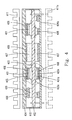
- FIG. 3 is a cross-sectional side view of a preferred embodiment of the power converter package according to the present invention. As shown, all the electrical connections for a power converter are achieved by fully being mounted onto a multi-layer PCB 402 in order to have a high interconnection density.
- a heat spreader 404 is directly attached onto a bare top heat-slug 405 of the sub-packages 401 and magnetic element 407 through a thermally conductive insulator 406 .
- the magnetic element 407 can be mounted into cutouts of the PCB 402 or be mounted onto top-side of the PCB 402 .
- the control device 408 and passive part 409 can be mounted onto one side or both sides of the PCB 402 , and the heater spreader 404 can also be attached onto them.
- a hard epoxy cover 410 may be applied to isolate the components from environment.
- the sub-package 401 is disposed between the multi-layer PCB 402 and the heat spreader 404 .
- the multi-layer PCB 402 is adapted to be electrically connected with the leads 403 of the sub-package 401 to provide an electrically conductive pathway therebetween.
- the heat spreader 404 is adapted to be thermally connected with the heat-slug 405 of sub-package 401 through a thermally conductive insulator 406 to provide a thermally conductive pathway therebetween.
- the heat from the sub-package 401 can be directly transferred to the attached heat spreader 404 by the bare top heat-slug 405 of the sub-package 401 , and further transferred to the outside.
- the electrical connection is only occurred between the leads 403 of the sub-package 401 and the multi-layer PCB 402 .
- This assembly of the package realizes that the electrically conductive pathway is separate from the thermally conductive pathway, and hence achieves an enhanced thermal management.
- an additional heat sink 411 can be attached to the heat spreader 404 to increase its cooling area.
- the heat sink 411 can also be directly attached onto the bare top heat-slug 405 of sub-package 401 , and the magnetic element 407 through thermally conductive insulators.
- the sub-package 401 is mounted onto one surface of the PCB 402 by a plurality of symmetrically arranged leads such as dual, four or round-distributed lateral leads 403 , or balls, and thus has a good mechanical support for the heat spreader 404 , and is easy to provide a co-plane for the sub-package 401 during the mounting process. Accordingly, there are the same number of leads 403 on any two opposite sides of the sub-package 401 . Taking the round-distributed lateral leads 403 as an example, there are the same number of leads 403 on two sides with respect to an axis of the sub-package 401 .
- the sub-package 401 encounters a low thermo-mechanical stress since the heat-slug 405 is attached to the heat spreader 404 with the thermally conductive insulator 406 . Therefore, the assembly of the present invention has not only the excellent thermal performance and high interconnection density, but good manufacturability and low cost as well.
- the heat-slug 405 of the sub-package 401 can be selected from a material of metal, ceramic, metal matrix composite and insulated metal substrate and the combination thereof, whether conventional or later-developed.
- the plurality of symmetric leads 403 can be selected from: dual, four, and round-distributed lateral leads.
- the multi-layer circuit board 400 can be selected from: copper clad laminates and a ceramic hybrid circuit board.
- the heat spreader 404 can be selected from the group substantially consisting of: metal, ceramic, and metal matrix composite and the combination thereof
- the sub-package with at least a power-dissipating chip 401 , 401 a can also be mounted onto both sides of the PCB 402 .
- Both heat spreaders 404 , 404 a can be attached from both sides of the assembly by the thermally conductive insulator 406 , and thus the heat from the sub-packages 401 , 401 a mounted onto both sides of the PCB 402 can be directly transferred by their bare top heat-slugs 405 , 405 a to the heat spreaders 404 , 404 a , and further transferred to the outside.
- the magnetic element 407 can be connected with heat spreaders 404 , 404 a from both sides with the thermally conductive insulator 406 .
- Other components such as control device 408 and passive component 409 with low power loss can also be thermally connected with the heat spreader from both sides.
- the packaging approach of the present invention can also be used for vertical mounting converters.
- FIG. 5 a shows the construction of the sub-package 401 in FIG. 3 a used for the present invention.
- the trimming of the leads are performed to make the bare heat-slug 405 face upwards and the leads 403 face downwards.
- the power-dissipating chips 416 , 416 a and passive chip 417 are directly attached onto the heat-slug 405 , wherein the heat-slug 405 can be isolated metal substrate (IMS) or metallizted ceramic substrate.
- IMS isolated metal substrate
- TAB tape automatic bond
- An epoxy or molding compound 415 can be used to seal the package and keep the outer surface of the heat-slug 405 bare.
- the leads 403 can be constructed in a symmetric arrangement such as dual, four or round-distributed lateral leads, wherein the trimming is performed to provide facing down leads 403 for surface mounting to PCB and to provide facing up heat-slug 405 for thermal connection.
- the package can be electrically connected with the PCB by leads 403 . Through this assembly a heat spreader can be directly attached to the bare top heat-slug 405 with the thermally conductive insulator to achieve the thermal connection of the power-dissipating chips 416 , 416 a to the outside.
- heat from the power-dissipating chips 416 , 416 a is transferred to the heat spreader 405 by the top heat-slug 405 , and further transferred to the ambient by the heat spreader 405 and therefore the PCB can be kept cool.
- the sub-package 401 in FIG. 5 a can also be constructed in the form as shown in FIG. 5 b .
- the leads 403 are replaced by the balls 403 a .
- the balls 403 a have lower profile and lower interconnection parasites than those of leads 403 , and thus the electrical performance can be further improved.
- power-dissipating chips 416 , 416 a , control device chips (not shown) and passive chips 417 can be combined into one sub-package.
- the sub-package can be simplified to be a standard surface-mounting package with a bare top up-facing heat-slug while the sub-package holds only one chip 416 .
- FIG. 6 a A derivative packaging art for the sub-package of FIG. 5 a is proposed to satisfy miscellaneous applications.
- the discrete power-dissipating devices 501 , 501 a have a bare bottom heat-slug 502 and electrical connection leads 503 , and are connected with the heat-slug 504 of the sub-package 500 a by the bare bottom heat-slug 502 and leads 503 to provide both electrical and thermal connections between the discrete power-dissipating devices 501 , 501 a and the heat-slug 504 of the sub-package 500 a .
- the heat-slug 504 of the sub-package 401 can be selected from a material of metal, ceramic, metal matrix composite and insulated metal substrate and the combination thereof
- the control device 505 and passive component 506 are also connected with the heat-slug 504 of the sub-package 500 a .
- the electrical interconnection within the discrete power-dissipating devices 501 , 501 a , the control device 505 and the passive component 506 are achieved by conductive trace (not shown) on the facing-down surface of the heat-slug 504 .
- the sub-package 500 a is electrically connected with the motherboard of a power converter by the plurality of symmetric leaded terminals 507 , and is thermally connected to the outside by the heat-slug 504 . Therefore the electrical conductive pathway of the sub-package 500 a is separate from the thermal conductive pathway.
- a plurality of symmetric balls 507 a can also be responsible for the electrical connection between the sub-package 500 b and the motherboard of a power converter.
Abstract
A package for power converters in which all parts are electrically connected with one multi-layer circuit board. A sub-package with at least a power-dissipating chip, having a bare top up-facing heat-slug is electrically connected with the board by a plurality of symmetric leads. A heat spreader is directly attached onto the bare top heat-slug of the sub-packages, planar magnetic parts and top surfaces of other components with thermally conductive insulator. The heat dissipated by the sub-packages is transferred to the attached heat spreader by the bare top heat-slug, and further transferred to the ambient. The assembly features compact and inexpensive power converter package with improved electrical performance and enhanced thermal management.
Description
- This invention relates to the packaging and assembly of electrical components, and more particularly to the packaging and assembly for power converters with enhanced thermal management, high electrical interconnection density and low profile.
- Please refer to FIG. 1. FIG. 1 shows one approach to package electric components in a power converter according to the prior art. As shown in FIG. 1, power-dissipating devices such as 9 b, 9 d and a
magnetic element 9 c are mounted directly on a metal base-plate 6 by a thermallyconductive insulator 8 for better heat transfer. The power components are electrically connected with aPCB 5 a by single-lateral leads 12. Themagnetic element 9 c is electrically connected toPCB 5 a by leaded terminals. And, other necessary components such as 9 a, 9 e are mounted to one side or both sides of the PCB 5 a. The assembly may be encapsulated within a capsule (not shown), which acts as a heat spreader and mechanical support. - One drawback of the packaging art in FIG. 1, however, is that since the power-
dissipating devices 9 b, 9 d are electrically connected with thePCB 5 a by the single-lateral leads 12, it will be difficult to keep these devices co-planar during the mounting process, which would make the overall manufacturing process more complex, and thus would undesirably increase the manufacturing cost. Meanwhile, the leaded electrical connections of power dissipation devices as well as magnetic element will cause high interconnection parasites, which will result in additional connection resistance loss and poor converter performance especially for high current converter packaging. Moreover, the power-dissipating devices 9 b, 9 d are comparatively in a bigger footprint, which would inevitably cause a lower power density packaging. - U.S. Pat. No. 5,973,923 discloses another prior art approach to package electronic components in a power converter as shown in FIG. 2. In the packaging, a thermal connection from a power-dissipating
device 22 to the outside is constructed, in which copper coatedvias 42 are prepared by the manufacturing process of the PCB 28. Themetal slug 43 of the power-dissipating device 22 is mounted onto the top pad of the copper coatedvias 42, and a metal base-plate 32 is attached to the bottom pad of the copper coatedvias 42 through thermallyconductive insulators vias 42, the heat is transferred from the power-dissipating device 22 to the other side of thePCB 28, and further transferred to the metal base-plate 32. Themagnetic element 26 b is also mounted on thePCB 28, and is connected with metal base-plate 32 by a thermally conductivesoft pad 34 to enhance the heat transfer. - One drawback of the packaging art in FIG. 2, however, is that since the power-
dissipating device 22 is mounted onto top-side of the copper coatedvias 42, and the bottom-side of the copper coated via is occupied by thethermal connections board 28. Moreover, heat from thepower device 22 will meanwhile be transferred by the copper coatedvias 42 to theboard 28, and thereby increases temperature rise of theboard 28. - With increasing power density and current output capability of the power converter packaging, much more power-dissipating devices are to be mounted onto PCB in parallel to satisfy high current output and meanwhile to well control the conduction power losses. Thus more and more PCB lands are to be occupied by power-dissipating devices. Moreover, the power losses from power-dissipation devices and its conductive trace increase abruptly with the increase of the output current. With the increase of power density and output current, how to manage the heat from these power-dissipating devices and how to shorten the interconnection trace therebetween become very critical for power converter packaging.
- It is therefore an object of the present invention to propose a packaging technology for power converters to achieve enhanced thermal management, high interconnection density, improved electrical performance as well as low cost.
- To address the above-discussed deficiencies of the prior art, the present invention provides, a package for a power converter, a method of packaging a power converter and a sub-package arrangement employed in the package of the present invention. The package includes: (1) a multi-layer circuit board having a first electrically conductive surface and a second electrically conductive surface opposite to the first electrically conductive surface; (2) a heat spreader having at least a heat transfer surface; and (3) a sub-package having at least a power-dissipating chip, which is disposed between one of the electrically conductive surfaces of the multi-layer circuit board and the heat transfer surface of the heat spreader, having a bare top heat-slug in contact with the heat transfer surface of the heat spreader through a thermally conductive insulator to provide a thermally conductive pathway therebetween, and having a plurality of symmetric leads in contact with one of the electrically conductive surfaces of the multi-layer circuit board to provide an electrically conductive pathway therebetween, wherein the plurality of symmetric leads and the heat-slug are disposed in opposite orientations so that the electrically conductive pathway is separate from the thermally conductive pathway.
- In one embodiment of the present invention, the plurality of symmetric leads can also be replaced by balls to meet some electrical connection requirements.
- In the present invention, the sub-package, magnetic elements and other passive components of the package are fully mounted onto a multi-layer circuit board.
- The unique aspect of this packaging concept is that the power-dissipating chips of the package, which are typically power semiconductors, are assembled in advance into the sub-package, therefore enabling the package to have high interconnection density. The sub-package has a bare top heat-slug and a plurality of symmetric leads (or balls), wherein the plurality of symmetric leads and the heat-slug are disposed in opposite orientations. In one embodiment of the present invention, the heat-slug is up-facing and the leads are down-facing. Of course, the heat-slug can also be down-facing and the leads be up-facing.
- In the present invention, the sub-package is disposed between the electrically conductive surface of the multi-layer circuit board and the heat transfer surface of the heat spreader. In this way, the first electrically conductive surface of the multi-layer circuit board is adapted to be electrically connected with the leads of the sub-package to provide an electrically conductive pathway therebetween. The heat transfer surface of the heat spreader is adapted to be thermally connected with the heat-slug of the sub-package through a thermally conductive insulator to provide a thermally conductive pathway therebetween. The heat from the magnetic elements can also be transferred to the ambient by the attached heat spreader. Therefore, the electrically conductive pathway is separate from the thermally conductive pathway, which achieves enhanced thermal management and improved electrical performance.
- In one embodiment of the present invention, the sub-package further includes control chips and passive chips. For the reason of increased packaging density and improved electrical performance, the power-dissipating chips, control chips and passive chips can be combined into one sub-package together. More specifically, the sub-package with only one chip can be simplified to be a standard surface-mounting package with a bare top up-facing heat-slug.
- Another aspect of the present invention provides a method of packaging a power converter including: (1) providing a multi-layer circuit board having at least an electrically conductive surface; (2) providing a heat spreader having at least a heat transfer surface; and (3) disposing the sub-package having at least a power-dissipating chip between the electrically conductive surface of the multi-layer circuit board and the heat transfer surface of the heat spreader, the sub-package having bare top up-facing heat-slug and a plurality of symmetric down-facing leads, whereby the electrically conductive surface of the multi-layer circuit board is adapted to be electrically connected with the leads of the sub-package to provide an electrically conductive pathway therebetween; the heat transfer surface of the heat spreader is adapted to be thermally connected with the heat-slug of the sub-package with at least a power-dissipating chip through a thermally conductive insulator to provide a thermally conductive pathway therebetween; and the electrically conductive pathway is separate from the thermally conductive pathway.
- Another aspect of the present invention provides a sub-package. In order to satisfy miscellaneous applications, a derivative art is proposed for the sub-package. In the art, the leaded discrete power-dissipating devices have a bare bottom heat-slug and are electrically and thermally connected with the heat-slug of the sub-package. The control devices and passive components are electrical connected with the power-dissipating devices by the conductive trace on the bottom surface of the heat-slug of the sub-package. The sub-package is electrically connected to the mother-board of a power converter by a plurality of symmetric leaded terminals or balls, and is thermally connected to the outside by the heat-slug of the sub-package. Therefore, the electrical conductive pathway of the sub-package is separate from the thermal conductive pathway.
- The present invention may best be understood through the following description with reference to the accompanying drawings, in which:
- FIG. 1 is a cross-sectional side view of the prior art for a power converter package wherein a power dissipation device with single-lateral leads is attached to a metal base-plate;
- FIG. 2 is a cross-sectional side view of the prior art for a power converter package wherein heat from a power dissipation device is transferred through copper coated vias of a PCB;
- FIG. 3 is a cross-sectional side view of a power converter packaging according to the present invention, wherein the sub-package with power dissipating chips are mounted to one side of a PCB;
- FIG. 3 a is a magnified picture for assembly of the sub-package with power dissipating chips in FIG. 3;
- FIG. 4 is a cross-sectional side view of a power converter package according to the present invention, wherein the sub-packages with at least a power-dissipating chip are mounted to both sides of the PCB;
- FIG. 5 a is a cross-sectional side view of the sub-package with at least a power-dissipating chip, and a top heat-slug and facing down leads according to the present invention;
- FIG. 5 b is a cross-sectional side view of the sub-package with at least a power-dissipating chip, and a top heat-slug and facing down balls according to the present invention;
- FIG. 6 a is a cross-sectional side view of the sub-package with at least a discrete power-dissipating package, and a top heat-slug and facing down leads according to the present invention; and
- FIG. 6 b is a cross-sectional side view of the sub-package with at least a discrete power-dissipating package, and a top heat-slug and facing down balls according to the present invention.
- FIG. 3 is a cross-sectional side view of a preferred embodiment of the power converter package according to the present invention. As shown, all the electrical connections for a power converter are achieved by fully being mounted onto a
multi-layer PCB 402 in order to have a high interconnection density. Aheat spreader 404 is directly attached onto a bare top heat-slug 405 of the sub-packages 401 andmagnetic element 407 through a thermallyconductive insulator 406. Themagnetic element 407 can be mounted into cutouts of thePCB 402 or be mounted onto top-side of thePCB 402. Thecontrol device 408 andpassive part 409 can be mounted onto one side or both sides of thePCB 402, and theheater spreader 404 can also be attached onto them. Ahard epoxy cover 410 may be applied to isolate the components from environment. - As can be seen, in the present invention, the sub-package 401 is disposed between the
multi-layer PCB 402 and theheat spreader 404. In this way, themulti-layer PCB 402 is adapted to be electrically connected with theleads 403 of the sub-package 401 to provide an electrically conductive pathway therebetween. Theheat spreader 404 is adapted to be thermally connected with the heat-slug 405 of sub-package 401 through a thermallyconductive insulator 406 to provide a thermally conductive pathway therebetween. - The heat from the sub-package 401 can be directly transferred to the attached
heat spreader 404 by the bare top heat-slug 405 of the sub-package 401, and further transferred to the outside. The electrical connection, however, is only occurred between theleads 403 of the sub-package 401 and themulti-layer PCB 402. This assembly of the package realizes that the electrically conductive pathway is separate from the thermally conductive pathway, and hence achieves an enhanced thermal management. - In applications wherein the power dissipated by the sub-package 401 cannot be easily cooled due to the limited surface of the
heat spreader 404, anadditional heat sink 411 can be attached to theheat spreader 404 to increase its cooling area. Hence theheat sink 411 can also be directly attached onto the bare top heat-slug 405 of sub-package 401, and themagnetic element 407 through thermally conductive insulators. The sub-package 401 is mounted onto one surface of thePCB 402 by a plurality of symmetrically arranged leads such as dual, four or round-distributed lateral leads 403, or balls, and thus has a good mechanical support for theheat spreader 404, and is easy to provide a co-plane for the sub-package 401 during the mounting process. Accordingly, there are the same number ofleads 403 on any two opposite sides of the sub-package 401. Taking the round-distributed lateral leads 403 as an example, there are the same number ofleads 403 on two sides with respect to an axis of the sub-package 401. - The sub-package 401 encounters a low thermo-mechanical stress since the heat-
slug 405 is attached to theheat spreader 404 with the thermallyconductive insulator 406. Therefore, the assembly of the present invention has not only the excellent thermal performance and high interconnection density, but good manufacturability and low cost as well. - Those skilled in the pertinent art will understand, however, that the heat-
slug 405 of the sub-package 401 can be selected from a material of metal, ceramic, metal matrix composite and insulated metal substrate and the combination thereof, whether conventional or later-developed. The plurality ofsymmetric leads 403 can be selected from: dual, four, and round-distributed lateral leads. The multi-layer circuit board 400 can be selected from: copper clad laminates and a ceramic hybrid circuit board. Theheat spreader 404 can be selected from the group substantially consisting of: metal, ceramic, and metal matrix composite and the combination thereof - In an alternative embodiment, referring to FIG. 4, the sub-package with at least a power-dissipating
chip PCB 402. Bothheat spreaders conductive insulator 406, and thus the heat from the sub-packages 401, 401 a mounted onto both sides of thePCB 402 can be directly transferred by their bare top heat-slugs 405, 405 a to theheat spreaders magnetic element 407 can be connected withheat spreaders conductive insulator 406. Other components such ascontrol device 408 andpassive component 409 with low power loss can also be thermally connected with the heat spreader from both sides. Thus the assembly further enhances thermal management of the power converter, and achieves a higher power density and a low profile power converter. The packaging approach of the present invention can also be used for vertical mounting converters. - FIG. 5 a shows the construction of the sub-package 401 in FIG. 3a used for the present invention. To improve the thermal characteristics, a development of the invention is provided in that the trimming of the leads are performed to make the bare heat-
slug 405 face upwards and theleads 403 face downwards. As shown in the FIG. 5a, the power-dissipatingchips passive chip 417 are directly attached onto the heat-slug 405, wherein the heat-slug 405 can be isolated metal substrate (IMS) or metallizted ceramic substrate. The wire bond or tape automatic bond (TAB) 414 . . . etc. can be used for the interconnection of chip to theconductive trace 418. An epoxy ormolding compound 415 can be used to seal the package and keep the outer surface of the heat-slug 405 bare. The leads 403 can be constructed in a symmetric arrangement such as dual, four or round-distributed lateral leads, wherein the trimming is performed to provide facing down leads 403 for surface mounting to PCB and to provide facing up heat-slug 405 for thermal connection. The package can be electrically connected with the PCB by leads 403. Through this assembly a heat spreader can be directly attached to the bare top heat-slug 405 with the thermally conductive insulator to achieve the thermal connection of the power-dissipatingchips chips heat spreader 405 by the top heat-slug 405, and further transferred to the ambient by theheat spreader 405 and therefore the PCB can be kept cool. - Please refer to FIG. 5 b. The sub-package 401 in FIG. 5a can also be constructed in the form as shown in FIG. 5b. Based on the structure of FIG. 5a, the
leads 403 are replaced by theballs 403 a. Theballs 403 a have lower profile and lower interconnection parasites than those ofleads 403, and thus the electrical performance can be further improved. For the reasons of increased packaging density and improved electrical performance, power-dissipatingchips passive chips 417 can be combined into one sub-package. The sub-package can be simplified to be a standard surface-mounting package with a bare top up-facing heat-slug while the sub-package holds only onechip 416. - Please refer to FIG. 6 a. A derivative packaging art for the sub-package of FIG. 5a is proposed to satisfy miscellaneous applications. In the art, the discrete power-dissipating
devices slug 502 and electrical connection leads 503, and are connected with the heat-slug 504 of the sub-package 500 a by the bare bottom heat-slug 502 and leads 503 to provide both electrical and thermal connections between the discrete power-dissipatingdevices slug 504 of the sub-package 500 a. Meanwhile, the heat-slug 504 of the sub-package 401 can be selected from a material of metal, ceramic, metal matrix composite and insulated metal substrate and the combination thereof Thecontrol device 505 andpassive component 506 are also connected with the heat-slug 504 of the sub-package 500 a. The electrical interconnection within the discrete power-dissipatingdevices control device 505 and thepassive component 506 are achieved by conductive trace (not shown) on the facing-down surface of the heat-slug 504. The sub-package 500 a is electrically connected with the motherboard of a power converter by the plurality of symmetricleaded terminals 507, and is thermally connected to the outside by the heat-slug 504. Therefore the electrical conductive pathway of the sub-package 500 a is separate from the thermal conductive pathway. - As shown in FIG. 6 b, a plurality of
symmetric balls 507 a can also be responsible for the electrical connection between the sub-package 500 b and the motherboard of a power converter. - While the invention has been described in terms of what are presently considered to be the most practical and preferred embodiments, it is to be understood that the invention needs not be limited to the disclosed embodiment. On the contrary, it is intended to cover various modifications and similar arrangements included within the spirit and scope of the appended claims, which are to be accorded with the broadest interpretation so as to encompass all such modifications and similar structures.
Claims (20)
1. A package for a power converter, comprising:
a multi-layer circuit board having a first electrically conductive surface and a second electrically conductive surface opposite to the first electrically conductive surface;
a heat spreader having at least a heat transfer surface; and
a sub-package having at least a power-dissipating chip, which is disposed between one of the electrically conductive surfaces of the multilayer circuit board and the heat transfer surface of the heat spreader, having a bare top heat-slug in contact with the heat transfer surface of the heat spreader through a thermally conductive insulator to provide a thermally conductive pathway therebetween, and having a plurality of symmetric leads in contact with one of the electrically conductive surfaces of the multilayer circuit board to provide an electrically conductive pathway therebetween, wherein the plurality of symmetric leads and the heat-slug are disposed in opposite orientations so that the electrically conductive pathway is separate from the thermally conductive pathway.
2. The package of claim 1 , wherein the heat-slug is up-facing and the leads are down-facing.
3. The package of claim 1 , wherein the heat-slug is down-facing and the leads are up-facing.
4. The package of claim 1 , wherein the heat-slug of the sub-package is selected from the group substantially consisting of metal, ceramic, metal matrix composite and insulated metal substrate and the combination thereof.
5. The package of claim 1 , wherein the plurality of symmetric leads are selected from the group substantially consisting of dual, four, round-distributed lateral leads.
6. The package of claim 1 , wherein the multi-layer circuit board is selected from the group substantially consisting of copper clad laminates and a ceramic hybrid circuit board.
7. The package of claim 1 , wherein the heat spreader is selected from the group substantially consisting of metal, ceramic, and metal matrix composite and the combination thereof.
8. The package of claim 1 , wherein the sub-package is mounted onto one surface of the multi-layer circuit board.
9. The package of claim 1 , wherein the sub-package is mounted onto both surfaces of the multi-layer circuit board.
10. A method of packaging a power converter, comprising:
providing a multi-layer circuit board having at least an electrically conductive surface;
providing a heat spreader having at least a heat transfer surface; and
disposing a sub-package having at least a power-dissipating chip between the electrically conductive surface of the multi-layer circuit board and the heat transfer surface of the heat spreader, the sub-package having a bare top heat-slug and a plurality of symmetric leads, wherein the electrically conductive surface of the multi-layer circuit board is adapted to be electrically connected with the leads of the sub-package to provide an electrically conductive pathway therebetween, the heat transfer surface of the heat spreader is adapted to be thermally connected with the heat-slug of the sub-package through a thermally conductive insulator to provide a thermally conductive pathway therebetween, and the electrically conductive pathway is separate from the thermally conductive pathway.
11. The method of claim 10 , wherein the heat-slug of the sub-package is selected from the group substantially consisting of metal, ceramic, metal matrix composite and insulated metal substrate and the combination thereof.
12. The method of claim 10 , wherein the plurality of symmetric leads are selected from the group substantially consisting of dual, four, round-distributed lateral leads.
13. The method of claim 10 , wherein the multi-layer circuit board is selected from the group substantially consisting of copper clad laminates and a ceramic hybrid circuit board.
14. The method of claim 10 , wherein the heat spreader is selected from the group substantially consisting of metal, ceramic, and metal matrix composite and the combination thereof.
15. The method of claim 10 , wherein the sub-package is mounted onto one surface of the multi-layer circuit board.
16. The method of claim 10 , wherein the sub-package is mounted onto both surfaces of the multi-layer circuit board.
17. A sub-package arranged in a package for a power converter, comprising:
at least a power-dissipating chip;
a substrate in contact with the power-dissipating chip for heat transfer from the power-dissipating chip to provide a thermally conductive pathway; and
a plurality of symmetric leads electrically connected to the power-dissipating chip to provide an electrically conductive pathway, wherein the plurality of symmetric leads and the substrate are disposed in opposite orientations so that an electrically conductive pathway is separate from a thermally conductive pathway.
18. The sub-package of claim 17 , wherein the substrate is selected from the group substantially consisting of: a ceramic substrate, an insulator metal substrate and a metal slug and the combination thereof.
19. A sub-package arranged in a package for a power converter, comprising:
at least a discrete power-dissipating device;
a substrate in contact with the discrete power-dissipating device for heat transfer from the discrete power-dissipating device to provide a thermally conductive pathway; and
a plurality of symmetric leads electrically connected to the discrete power-dissipating devices to provide an electrically conductive pathway, wherein the plurality of symmetric leads and the substrate are disposed in opposite orientations so that an electrically conductive pathway is separate from a thermally conductive pathway.
20. The sub-package of claim 19 , wherein the substrate further comprises control devices and passive components.
Priority Applications (3)
| Application Number | Priority Date | Filing Date | Title |
|---|---|---|---|
| US10/127,896 US6724631B2 (en) | 2002-04-22 | 2002-04-22 | Power converter package with enhanced thermal management |
| TW092106844A TW560229B (en) | 2002-04-22 | 2003-03-26 | Power converter package with enhanced thermal management |
| CNB031104827A CN100456472C (en) | 2002-04-22 | 2003-04-15 | Power converter package with enhanced thermal management |
Applications Claiming Priority (1)
| Application Number | Priority Date | Filing Date | Title |
|---|---|---|---|
| US10/127,896 US6724631B2 (en) | 2002-04-22 | 2002-04-22 | Power converter package with enhanced thermal management |
Publications (2)
| Publication Number | Publication Date |
|---|---|
| US20030198022A1 true US20030198022A1 (en) | 2003-10-23 |
| US6724631B2 US6724631B2 (en) | 2004-04-20 |
Family
ID=29215355
Family Applications (1)
| Application Number | Title | Priority Date | Filing Date |
|---|---|---|---|
| US10/127,896 Expired - Lifetime US6724631B2 (en) | 2002-04-22 | 2002-04-22 | Power converter package with enhanced thermal management |
Country Status (3)
| Country | Link |
|---|---|
| US (1) | US6724631B2 (en) |
| CN (1) | CN100456472C (en) |
| TW (1) | TW560229B (en) |
Cited By (35)
| Publication number | Priority date | Publication date | Assignee | Title |
|---|---|---|---|---|
| EP1524893A1 (en) * | 2003-10-03 | 2005-04-20 | C.R.F. Società Consortile per Azioni | Electronic control unit, in particular for motor vehicles, with improved heat dissipation system |
| FR2870667A1 (en) * | 2004-05-24 | 2005-11-25 | Mitsubishi Electric Corp | POWER CONVERSION DEVICE |
| WO2006069935A1 (en) * | 2004-12-28 | 2006-07-06 | Siemens Aktiengesellschaft | Electrical module comprising spacers between a plurality of circuit carriers |
| US20060274512A1 (en) * | 2005-06-06 | 2006-12-07 | Delphi Technologies, Inc. | Circuit assembly with surface-mount ic package and heat sink |
| US20110310560A1 (en) * | 2009-12-17 | 2011-12-22 | Nicholas Charles Leopold Jarmany | Electronic assembly and casing therefor |
| US20120314374A1 (en) * | 2011-03-11 | 2012-12-13 | Daniel Elkaslassy | Heat dissipating high power systems |
| US20130135824A1 (en) * | 2011-11-30 | 2013-05-30 | Hitachi, Ltd. | Power Semiconductor Device |
| CN103930986A (en) * | 2011-12-09 | 2014-07-16 | 富士电机株式会社 | Power conversion apparatus |
| US20140268579A1 (en) * | 2013-03-16 | 2014-09-18 | Henkel Corporation | Electronic devices assembled with heat absorbing and/or thermally insulating composition |
| US9101082B1 (en) * | 2010-05-03 | 2015-08-04 | Sunpower Corporation | Junction box thermal management |
| EP2919572A1 (en) * | 2014-03-14 | 2015-09-16 | DET International Holding Limited | Modular power supply |
| US20150289375A1 (en) * | 2012-11-01 | 2015-10-08 | Kabushiki Kaisha Toyota Jidoshokki | Module for facilitating positioning of electronic components |
| US20150351224A1 (en) * | 2014-06-03 | 2015-12-03 | Sumitomo Bakelite Co., Ltd. | Metal-based mounting board and member provided with metal-based mounting board |
| US20150351223A1 (en) * | 2014-06-03 | 2015-12-03 | Sumitomo Bakelite Co., Ltd. | Metal-based mounting board and member provided with metal-based mounting board |
| US9209104B2 (en) | 2011-11-15 | 2015-12-08 | Henkel IP & Holding GmbH | Electronic devices assembled with thermally insulating layers |
| US9209105B2 (en) | 2011-11-15 | 2015-12-08 | Henkel IP & Holding GmbH | Electronic devices assembled with thermally insulating layers |
| US9236324B2 (en) * | 2011-12-26 | 2016-01-12 | Mitsubishi Electric Corporation | Electric power semiconductor device and method for producing same |
| DE102014224995A1 (en) * | 2014-12-05 | 2016-06-09 | Siemens Aktiengesellschaft | Heat sink for cooling an electrical device |
| US20160262270A1 (en) * | 2015-03-04 | 2016-09-08 | International Business Machines Corporation | Electronic package with heat transfer element(s) |
| DE102012202576B4 (en) * | 2011-02-24 | 2017-02-16 | Denso Corporation | ELECTRONIC CONTROL UNIT |
| US9980365B1 (en) * | 2016-12-27 | 2018-05-22 | Msi Computer (Shenzhen) Co., Ltd. | Electronic device |
| EP2208225B1 (en) * | 2007-11-13 | 2018-10-10 | Siemens Aktiengesellschaft | Power semiconductor module |
| US10169968B1 (en) | 2016-02-25 | 2019-01-01 | International Business Machines Corporation | Multi-layer stack with embedded tamper-detect protection |
| EP3439160A1 (en) * | 2008-07-29 | 2019-02-06 | Hitachi, Ltd. | Power conversion apparatus and electric vehicle |
| US20190132995A1 (en) * | 2017-10-27 | 2019-05-02 | Micron Technology, Inc. | Assemblies including heat dispersing elements and related systems and methods |
| US20190157177A1 (en) * | 2017-11-22 | 2019-05-23 | Mitsubishi Electric Corporation | Semiconductor device |
| US10378925B2 (en) | 2015-09-25 | 2019-08-13 | International Business Machines Corporation | Circuit boards and electronic packages with embedded tamper-respondent sensor |
| DE102018205243A1 (en) * | 2018-04-09 | 2019-10-10 | Zf Friedrichshafen Ag | Electronic power control module and method of manufacturing an electronic power control module |
| US10481653B2 (en) | 2013-12-19 | 2019-11-19 | Henkel IP & Holding GmbH | Compositions having a matrix and encapsulated phase change materials dispersed therein, and electronic devices assembled therewith |
| US10531561B2 (en) | 2018-02-22 | 2020-01-07 | International Business Machines Corporation | Enclosure-to-board interface with tamper-detect circuit(s) |
| US10535618B2 (en) | 2016-05-13 | 2020-01-14 | International Business Machines Corporation | Tamper-proof electronic packages with stressed glass component substrate(s) |
| US10667389B2 (en) | 2016-09-26 | 2020-05-26 | International Business Machines Corporation | Vented tamper-respondent assemblies |
| US10685146B2 (en) | 2015-09-25 | 2020-06-16 | International Business Machines Corporation | Overlapping, discrete tamper-respondent sensors |
| DE102019218157A1 (en) * | 2019-11-25 | 2021-05-27 | Zf Friedrichshafen Ag | Power module with housed power semiconductors for the controllable electrical power supply of a consumer and a method for production |
| LU502675B1 (en) * | 2022-08-17 | 2024-02-20 | Rolls Royce Deutschland Ltd & Co Kg | Printed circuit board assembly |
Families Citing this family (26)
| Publication number | Priority date | Publication date | Assignee | Title |
|---|---|---|---|---|
| US6881077B2 (en) * | 2002-07-22 | 2005-04-19 | Siemens Vdo Automotive Corporation | Automotive control module housing |
| US7067903B2 (en) * | 2002-11-07 | 2006-06-27 | Kabushiki Kaisha Kobe Seiko Sho | Heat spreader and semiconductor device and package using the same |
| US7254033B2 (en) * | 2004-08-19 | 2007-08-07 | Behdad Jafari | Method and apparatus for heat dissipation |
| SE529673C2 (en) * | 2004-09-20 | 2007-10-16 | Danaher Motion Stockholm Ab | Circuit arrangement for cooling surface-mounted semiconductors |
| JP2007194830A (en) * | 2006-01-18 | 2007-08-02 | Mitsumi Electric Co Ltd | Tuner module |
| US7450387B2 (en) * | 2006-03-02 | 2008-11-11 | Tdk Innoveta Technologies, Inc. | System for cooling electronic components |
| DE102006018854A1 (en) * | 2006-04-22 | 2007-11-22 | Sma Technologie Ag | Housing of a power converter |
| US7515423B2 (en) * | 2006-09-22 | 2009-04-07 | Fu Zhun Precision Industry (Shen Zhen) Co., Ltd. | Heat dissipation device |
| US20080266786A1 (en) * | 2007-04-25 | 2008-10-30 | Behdad Jafari | Method and apparatus for heat dissipation |
| US8064202B2 (en) * | 2010-02-24 | 2011-11-22 | Monolithic Power Systems, Inc. | Sandwich structure with double-sided cooling and EMI shielding |
| US8531841B2 (en) * | 2010-10-26 | 2013-09-10 | Tdk-Lambda Corporation | IC thermal management system |
| US9119327B2 (en) | 2010-10-26 | 2015-08-25 | Tdk-Lambda Corporation | Thermal management system and method |
| US8514576B1 (en) * | 2011-06-14 | 2013-08-20 | Juniper Networks, Inc. | Dual sided system in a package |
| KR20140115668A (en) | 2013-03-21 | 2014-10-01 | 삼성전자주식회사 | Semiconductor package having a heat slug and a passive device |
| CN103200805A (en) * | 2013-04-03 | 2013-07-10 | 张家港市华力电子有限公司 | Heat radiation structure of electronic devices in sealed shell |
| CN103515249B (en) * | 2013-08-06 | 2016-02-24 | 江苏长电科技股份有限公司 | First be honored as a queen and lose three-dimensional systematic chip formal dress bump packaging structure and process |
| CN103400772B (en) * | 2013-08-06 | 2016-08-17 | 江阴芯智联电子科技有限公司 | First it is honored as a queen and loses chip formal dress three-dimensional systematic metallic circuit plate structure and process |
| CN103400774B (en) * | 2013-08-06 | 2016-01-20 | 江苏长电科技股份有限公司 | First be honored as a queen and lose chip formal dress salient point three-dimensional systematic metal circuit board and process |
| JP6278695B2 (en) * | 2013-12-26 | 2018-02-14 | 株式会社デンソー | Electronic control unit and electric power steering apparatus using the same |
| CN105814978B (en) | 2014-01-08 | 2018-06-22 | 恩菲斯能源公司 | Double insulation radiator |
| JP2015223044A (en) * | 2014-05-23 | 2015-12-10 | 株式会社オートネットワーク技術研究所 | Circuit structure and electric connection box |
| JP6693706B2 (en) * | 2015-04-06 | 2020-05-13 | 株式会社デンソー | Electronic control unit |
| JP6528620B2 (en) * | 2015-09-15 | 2019-06-12 | 株式会社オートネットワーク技術研究所 | Circuit structure and electrical connection box |
| EP3416467B1 (en) * | 2017-06-13 | 2022-05-04 | ABB Schweiz AG | Heat exchanger structure for a rack assembly |
| CN110290640A (en) * | 2019-07-31 | 2019-09-27 | 东莞市沃德普自动化科技有限公司 | A kind of equipment and its pcb board |
| US11791249B2 (en) | 2021-10-29 | 2023-10-17 | Texas Instruments Incorporated | Thermally enhanced isolated power converter package |
Family Cites Families (6)
| Publication number | Priority date | Publication date | Assignee | Title |
|---|---|---|---|---|
| US4914551A (en) * | 1988-07-13 | 1990-04-03 | International Business Machines Corporation | Electronic package with heat spreader member |
| US5396403A (en) * | 1993-07-06 | 1995-03-07 | Hewlett-Packard Company | Heat sink assembly with thermally-conductive plate for a plurality of integrated circuits on a substrate |
| US5883782A (en) * | 1997-03-05 | 1999-03-16 | Intel Corporation | Apparatus for attaching a heat sink to a PCB mounted semiconductor package |
| US6432497B2 (en) * | 1997-07-28 | 2002-08-13 | Parker-Hannifin Corporation | Double-side thermally conductive adhesive tape for plastic-packaged electronic components |
| US5973923A (en) | 1998-05-28 | 1999-10-26 | Jitaru; Ionel | Packaging power converters |
| US6428189B1 (en) * | 2000-03-31 | 2002-08-06 | Relume Corporation | L.E.D. thermal management |
-
2002
- 2002-04-22 US US10/127,896 patent/US6724631B2/en not_active Expired - Lifetime
-
2003
- 2003-03-26 TW TW092106844A patent/TW560229B/en not_active IP Right Cessation
- 2003-04-15 CN CNB031104827A patent/CN100456472C/en not_active Expired - Lifetime
Cited By (59)
| Publication number | Priority date | Publication date | Assignee | Title |
|---|---|---|---|---|
| EP1524893A1 (en) * | 2003-10-03 | 2005-04-20 | C.R.F. Società Consortile per Azioni | Electronic control unit, in particular for motor vehicles, with improved heat dissipation system |
| FR2870667A1 (en) * | 2004-05-24 | 2005-11-25 | Mitsubishi Electric Corp | POWER CONVERSION DEVICE |
| WO2006069935A1 (en) * | 2004-12-28 | 2006-07-06 | Siemens Aktiengesellschaft | Electrical module comprising spacers between a plurality of circuit carriers |
| US20060274512A1 (en) * | 2005-06-06 | 2006-12-07 | Delphi Technologies, Inc. | Circuit assembly with surface-mount ic package and heat sink |
| EP1732130A3 (en) * | 2005-06-06 | 2008-12-03 | Delphi Technologies, Inc. | Circuit assembly with surface-mount IC package and heat sink |
| US7561436B2 (en) | 2005-06-06 | 2009-07-14 | Delphi Technologies, Inc. | Circuit assembly with surface-mount IC package and heat sink |
| EP2208225B1 (en) * | 2007-11-13 | 2018-10-10 | Siemens Aktiengesellschaft | Power semiconductor module |
| EP3439160A1 (en) * | 2008-07-29 | 2019-02-06 | Hitachi, Ltd. | Power conversion apparatus and electric vehicle |
| US8373990B2 (en) * | 2009-12-17 | 2013-02-12 | Quixant Limited | Electronic assembly and casing therefor |
| US20110310560A1 (en) * | 2009-12-17 | 2011-12-22 | Nicholas Charles Leopold Jarmany | Electronic assembly and casing therefor |
| US10681829B2 (en) | 2010-05-03 | 2020-06-09 | Sunpower Corporation | Electrical junction box with removable sealing cover |
| US9101082B1 (en) * | 2010-05-03 | 2015-08-04 | Sunpower Corporation | Junction box thermal management |
| US9763360B2 (en) * | 2010-05-03 | 2017-09-12 | Sunpower Corporation | Serviceable electrical box thermal management |
| US20150342084A1 (en) * | 2010-05-03 | 2015-11-26 | Sunpower Corporation | Serviceable Electrical Box Thermal Management |
| DE102012202576B4 (en) * | 2011-02-24 | 2017-02-16 | Denso Corporation | ELECTRONIC CONTROL UNIT |
| US20120314374A1 (en) * | 2011-03-11 | 2012-12-13 | Daniel Elkaslassy | Heat dissipating high power systems |
| US8929081B2 (en) * | 2011-03-11 | 2015-01-06 | Marvell Israel (M.I.S.L) Ltd. | Heat dissipating high power systems |
| US9408308B2 (en) | 2011-03-11 | 2016-08-02 | Marvell Israel (M.I.S.L) Ltd. | Heat dissipating high power systems |
| US9209104B2 (en) | 2011-11-15 | 2015-12-08 | Henkel IP & Holding GmbH | Electronic devices assembled with thermally insulating layers |
| US9209105B2 (en) | 2011-11-15 | 2015-12-08 | Henkel IP & Holding GmbH | Electronic devices assembled with thermally insulating layers |
| US9013877B2 (en) * | 2011-11-30 | 2015-04-21 | Hitachi Power Semiconductor Device, Ltd. | Power semiconductor device |
| US20130135824A1 (en) * | 2011-11-30 | 2013-05-30 | Hitachi, Ltd. | Power Semiconductor Device |
| CN103930986A (en) * | 2011-12-09 | 2014-07-16 | 富士电机株式会社 | Power conversion apparatus |
| US9236324B2 (en) * | 2011-12-26 | 2016-01-12 | Mitsubishi Electric Corporation | Electric power semiconductor device and method for producing same |
| US20150289375A1 (en) * | 2012-11-01 | 2015-10-08 | Kabushiki Kaisha Toyota Jidoshokki | Module for facilitating positioning of electronic components |
| US20140268579A1 (en) * | 2013-03-16 | 2014-09-18 | Henkel Corporation | Electronic devices assembled with heat absorbing and/or thermally insulating composition |
| US9223363B2 (en) * | 2013-03-16 | 2015-12-29 | Henkel IP & Holding GmbH | Electronic devices assembled with heat absorbing and/or thermally insulating composition |
| US10481653B2 (en) | 2013-12-19 | 2019-11-19 | Henkel IP & Holding GmbH | Compositions having a matrix and encapsulated phase change materials dispersed therein, and electronic devices assembled therewith |
| US11155065B2 (en) | 2013-12-19 | 2021-10-26 | Henkel IP & Holding GmbH | Compositions having a matrix and encapsulated phase change materials dispersed therein, and electronic devices assembled therewith |
| EP2919572A1 (en) * | 2014-03-14 | 2015-09-16 | DET International Holding Limited | Modular power supply |
| EP3319407A1 (en) * | 2014-03-14 | 2018-05-09 | DET International Holding Limited | Modular power supply |
| US20150351224A1 (en) * | 2014-06-03 | 2015-12-03 | Sumitomo Bakelite Co., Ltd. | Metal-based mounting board and member provided with metal-based mounting board |
| US20150351223A1 (en) * | 2014-06-03 | 2015-12-03 | Sumitomo Bakelite Co., Ltd. | Metal-based mounting board and member provided with metal-based mounting board |
| DE102014224995A1 (en) * | 2014-12-05 | 2016-06-09 | Siemens Aktiengesellschaft | Heat sink for cooling an electrical device |
| US20160262270A1 (en) * | 2015-03-04 | 2016-09-08 | International Business Machines Corporation | Electronic package with heat transfer element(s) |
| US10237964B2 (en) * | 2015-03-04 | 2019-03-19 | International Business Machines Corporation | Manufacturing electronic package with heat transfer element(s) |
| US10378924B2 (en) | 2015-09-25 | 2019-08-13 | International Business Machines Corporation | Circuit boards and electronic packages with embedded tamper-respondent sensor |
| US10378925B2 (en) | 2015-09-25 | 2019-08-13 | International Business Machines Corporation | Circuit boards and electronic packages with embedded tamper-respondent sensor |
| US10685146B2 (en) | 2015-09-25 | 2020-06-16 | International Business Machines Corporation | Overlapping, discrete tamper-respondent sensors |
| US10217336B2 (en) | 2016-02-25 | 2019-02-26 | International Business Machines Corporation | Multi-layer stack with embedded tamper-detect protection |
| US10169967B1 (en) | 2016-02-25 | 2019-01-01 | International Business Machines Corporation | Multi-layer stack with embedded tamper-detect protection |
| US10169968B1 (en) | 2016-02-25 | 2019-01-01 | International Business Machines Corporation | Multi-layer stack with embedded tamper-detect protection |
| US10535618B2 (en) | 2016-05-13 | 2020-01-14 | International Business Machines Corporation | Tamper-proof electronic packages with stressed glass component substrate(s) |
| US10535619B2 (en) | 2016-05-13 | 2020-01-14 | International Business Machines Corporation | Tamper-proof electronic packages with stressed glass component substrate(s) |
| US10667389B2 (en) | 2016-09-26 | 2020-05-26 | International Business Machines Corporation | Vented tamper-respondent assemblies |
| US9980365B1 (en) * | 2016-12-27 | 2018-05-22 | Msi Computer (Shenzhen) Co., Ltd. | Electronic device |
| US20190132995A1 (en) * | 2017-10-27 | 2019-05-02 | Micron Technology, Inc. | Assemblies including heat dispersing elements and related systems and methods |
| US11617284B2 (en) | 2017-10-27 | 2023-03-28 | Micron Technology, Inc. | Assemblies including heat dispersing elements and related systems and methods |
| US10952352B2 (en) * | 2017-10-27 | 2021-03-16 | Micron Technology, Inc. | Assemblies including heat dispersing elements and related systems and methods |
| CN109817590A (en) * | 2017-11-22 | 2019-05-28 | 三菱电机株式会社 | Semiconductor device |
| US10643918B2 (en) * | 2017-11-22 | 2020-05-05 | Mitsubishi Electric Corporation | Semiconductor device |
| JP2019096718A (en) * | 2017-11-22 | 2019-06-20 | 三菱電機株式会社 | Semiconductor device |
| US20190157177A1 (en) * | 2017-11-22 | 2019-05-23 | Mitsubishi Electric Corporation | Semiconductor device |
| US10531561B2 (en) | 2018-02-22 | 2020-01-07 | International Business Machines Corporation | Enclosure-to-board interface with tamper-detect circuit(s) |
| US11083082B2 (en) | 2018-02-22 | 2021-08-03 | International Business Machines Corporation | Enclosure-to-board interface with tamper-detect circuit(s) |
| DE102018205243A1 (en) * | 2018-04-09 | 2019-10-10 | Zf Friedrichshafen Ag | Electronic power control module and method of manufacturing an electronic power control module |
| US11062972B2 (en) | 2018-04-09 | 2021-07-13 | Zf Friedrichshafen Ag | Electronic module for power control and method for manufacturing an electronic module power control |
| DE102019218157A1 (en) * | 2019-11-25 | 2021-05-27 | Zf Friedrichshafen Ag | Power module with housed power semiconductors for the controllable electrical power supply of a consumer and a method for production |
| LU502675B1 (en) * | 2022-08-17 | 2024-02-20 | Rolls Royce Deutschland Ltd & Co Kg | Printed circuit board assembly |
Also Published As
| Publication number | Publication date |
|---|---|
| TW560229B (en) | 2003-11-01 |
| TW200306138A (en) | 2003-11-01 |
| CN1638114A (en) | 2005-07-13 |
| CN100456472C (en) | 2009-01-28 |
| US6724631B2 (en) | 2004-04-20 |
Similar Documents
| Publication | Publication Date | Title |
|---|---|---|
| US6724631B2 (en) | Power converter package with enhanced thermal management | |
| US8309399B2 (en) | Power semiconductor module and method of manufacturing the same | |
| US8916958B2 (en) | Semiconductor package with multiple chips and substrate in metal cap | |
| US5886408A (en) | Multi-chip semiconductor device | |
| US6029343A (en) | Insulated surface mount circuit board construction | |
| US8890310B2 (en) | Power module package having excellent heat sink emission capability and method for manufacturing the same | |
| US6972479B2 (en) | Package with stacked substrates | |
| US20140029201A1 (en) | Power package module and manufacturing method thereof | |
| US7551455B2 (en) | Package structure | |
| US7786571B2 (en) | Heat-conductive package structure | |
| KR20090034889A (en) | Chip module for complete power train | |
| KR20010104308A (en) | Power semiconductor module | |
| CN111261598A (en) | Packaging structure and power module applicable to same | |
| US20230260693A1 (en) | MAGNETIC DEVICE and STACKED ELECTRONIC STRUCTURE | |
| JPH11191603A (en) | Semiconductor integrated circuit and its manufacture | |
| US7309838B2 (en) | Multi-layered circuit board assembly with improved thermal dissipation | |
| US7564128B2 (en) | Fully testable surface mount die package configured for two-sided cooling | |
| JPH09199823A (en) | Chip-on-board printed wiring board | |
| CN210379025U (en) | Power device packaging structure | |
| US20050006758A1 (en) | Method for packaging electronic modules and multiple chip packaging | |
| KR20220015220A (en) | Power module and manufacturing method thereof | |
| US6278190B1 (en) | Semiconductor device | |
| JPH07335789A (en) | Package | |
| KR20220003807A (en) | Ceramic substrate and power module | |
| KR101090038B1 (en) | Multi-layered circuit board assembly |
Legal Events
| Date | Code | Title | Description |
|---|---|---|---|
| AS | Assignment |
Owner name: DELTA ELECTRONICS, INC., TAIWAN Free format text: ASSIGNMENT OF ASSIGNORS INTEREST;ASSIGNORS:YE, RUNQING;ZHANG, ALPHA J.;REEL/FRAME:012824/0922 Effective date: 20020410 |
|
| STCF | Information on status: patent grant |
Free format text: PATENTED CASE |
|
| FPAY | Fee payment |
Year of fee payment: 4 |
|
| FPAY | Fee payment |
Year of fee payment: 8 |
|
| FPAY | Fee payment |
Year of fee payment: 12 |