US20030198830A1 - Organic electroluminescent devices having encapsulation thin film formed by wet processing and methods for manufacturing the same - Google Patents
Organic electroluminescent devices having encapsulation thin film formed by wet processing and methods for manufacturing the same Download PDFInfo
- Publication number
- US20030198830A1 US20030198830A1 US10/392,131 US39213103A US2003198830A1 US 20030198830 A1 US20030198830 A1 US 20030198830A1 US 39213103 A US39213103 A US 39213103A US 2003198830 A1 US2003198830 A1 US 2003198830A1
- Authority
- US
- United States
- Prior art keywords
- irgacure
- organic electroluminescent
- electroluminescent device
- vinyl monomer
- initiator
- Prior art date
- Legal status (The legal status is an assumption and is not a legal conclusion. Google has not performed a legal analysis and makes no representation as to the accuracy of the status listed.)
- Granted
Links
- 238000005538 encapsulation Methods 0.000 title claims abstract description 65
- 238000000034 method Methods 0.000 title claims abstract description 32
- 238000004519 manufacturing process Methods 0.000 title claims abstract description 16
- 239000010409 thin film Substances 0.000 title 1
- 239000000178 monomer Substances 0.000 claims abstract description 51
- 229920002554 vinyl polymer Polymers 0.000 claims abstract description 44
- 125000000391 vinyl group Chemical group [H]C([*])=C([H])[H] 0.000 claims abstract description 37
- 229920000642 polymer Polymers 0.000 claims abstract description 33
- 239000003505 polymerization initiator Substances 0.000 claims abstract description 27
- 238000006116 polymerization reaction Methods 0.000 claims abstract description 16
- 239000000758 substrate Substances 0.000 claims abstract description 14
- 239000003999 initiator Substances 0.000 claims description 43
- RIWRBSMFKVOJMN-UHFFFAOYSA-N 2-methyl-1-phenylpropan-2-ol Chemical compound CC(C)(O)CC1=CC=CC=C1 RIWRBSMFKVOJMN-UHFFFAOYSA-N 0.000 claims description 16
- QVGXLLKOCUKJST-UHFFFAOYSA-N atomic oxygen Chemical compound [O] QVGXLLKOCUKJST-UHFFFAOYSA-N 0.000 claims description 15
- 239000001301 oxygen Substances 0.000 claims description 15
- 229910052760 oxygen Inorganic materials 0.000 claims description 15
- MHAJPDPJQMAIIY-UHFFFAOYSA-N Hydrogen peroxide Chemical compound OO MHAJPDPJQMAIIY-UHFFFAOYSA-N 0.000 claims description 12
- ZQMIGQNCOMNODD-UHFFFAOYSA-N diacetyl peroxide Chemical compound CC(=O)OOC(C)=O ZQMIGQNCOMNODD-UHFFFAOYSA-N 0.000 claims description 12
- XXQBEVHPUKOQEO-UHFFFAOYSA-N potassium superoxide Chemical compound [K+].[K+].[O-][O-] XXQBEVHPUKOQEO-UHFFFAOYSA-N 0.000 claims description 12
- -1 acryl Chemical group 0.000 claims description 11
- KWVGIHKZDCUPEU-UHFFFAOYSA-N 2,2-dimethoxy-2-phenylacetophenone Chemical compound C=1C=CC=CC=1C(OC)(OC)C(=O)C1=CC=CC=C1 KWVGIHKZDCUPEU-UHFFFAOYSA-N 0.000 claims description 10
- OZAIFHULBGXAKX-UHFFFAOYSA-N 2-(2-cyanopropan-2-yldiazenyl)-2-methylpropanenitrile Chemical compound N#CC(C)(C)N=NC(C)(C)C#N OZAIFHULBGXAKX-UHFFFAOYSA-N 0.000 claims description 10
- PPBRXRYQALVLMV-UHFFFAOYSA-N Styrene Chemical compound C=CC1=CC=CC=C1 PPBRXRYQALVLMV-UHFFFAOYSA-N 0.000 claims description 10
- 230000002745 absorbent Effects 0.000 claims description 10
- 239000002250 absorbent Substances 0.000 claims description 10
- VFHVQBAGLAREND-UHFFFAOYSA-N diphenylphosphoryl-(2,4,6-trimethylphenyl)methanone Chemical compound CC1=CC(C)=CC(C)=C1C(=O)P(=O)(C=1C=CC=CC=1)C1=CC=CC=C1 VFHVQBAGLAREND-UHFFFAOYSA-N 0.000 claims description 10
- UHFFVFAKEGKNAQ-UHFFFAOYSA-N 2-benzyl-2-(dimethylamino)-1-(4-morpholin-4-ylphenyl)butan-1-one Chemical compound C=1C=C(N2CCOCC2)C=CC=1C(=O)C(CC)(N(C)C)CC1=CC=CC=C1 UHFFVFAKEGKNAQ-UHFFFAOYSA-N 0.000 claims description 9
- DNIAPMSPPWPWGF-UHFFFAOYSA-N Propylene glycol Chemical compound CC(O)CO DNIAPMSPPWPWGF-UHFFFAOYSA-N 0.000 claims description 9
- MTPIZGPBYCHTGQ-UHFFFAOYSA-N 2-[2,2-bis(2-prop-2-enoyloxyethoxymethyl)butoxy]ethyl prop-2-enoate Chemical compound C=CC(=O)OCCOCC(CC)(COCCOC(=O)C=C)COCCOC(=O)C=C MTPIZGPBYCHTGQ-UHFFFAOYSA-N 0.000 claims description 8
- LWRBVKNFOYUCNP-UHFFFAOYSA-N 2-methyl-1-(4-methylsulfanylphenyl)-2-morpholin-4-ylpropan-1-one Chemical compound C1=CC(SC)=CC=C1C(=O)C(C)(C)N1CCOCC1 LWRBVKNFOYUCNP-UHFFFAOYSA-N 0.000 claims description 8
- 239000011248 coating agent Substances 0.000 claims description 8
- 238000000576 coating method Methods 0.000 claims description 8
- GJKGAPPUXSSCFI-UHFFFAOYSA-N 2-Hydroxy-4'-(2-hydroxyethoxy)-2-methylpropiophenone Chemical compound CC(C)(O)C(=O)C1=CC=C(OCCO)C=C1 GJKGAPPUXSSCFI-UHFFFAOYSA-N 0.000 claims description 7
- VEXZGXHMUGYJMC-UHFFFAOYSA-M Chloride anion Chemical compound [Cl-] VEXZGXHMUGYJMC-UHFFFAOYSA-M 0.000 claims description 7
- YQHLDYVWEZKEOX-UHFFFAOYSA-N cumene hydroperoxide Chemical compound OOC(C)(C)C1=CC=CC=C1 YQHLDYVWEZKEOX-UHFFFAOYSA-N 0.000 claims description 7
- NIXOWILDQLNWCW-UHFFFAOYSA-M Acrylate Chemical compound [O-]C(=O)C=C NIXOWILDQLNWCW-UHFFFAOYSA-M 0.000 claims description 6
- 239000004342 Benzoyl peroxide Substances 0.000 claims description 6
- OMPJBNCRMGITSC-UHFFFAOYSA-N Benzoylperoxide Chemical compound C=1C=CC=CC=1C(=O)OOC(=O)C1=CC=CC=C1 OMPJBNCRMGITSC-UHFFFAOYSA-N 0.000 claims description 6
- OYPRJOBELJOOCE-UHFFFAOYSA-N Calcium Chemical compound [Ca] OYPRJOBELJOOCE-UHFFFAOYSA-N 0.000 claims description 6
- RTZKZFJDLAIYFH-UHFFFAOYSA-N Diethyl ether Chemical compound CCOCC RTZKZFJDLAIYFH-UHFFFAOYSA-N 0.000 claims description 6
- VYPSYNLAJGMNEJ-UHFFFAOYSA-N Silicium dioxide Chemical compound O=[Si]=O VYPSYNLAJGMNEJ-UHFFFAOYSA-N 0.000 claims description 6
- 229910021536 Zeolite Inorganic materials 0.000 claims description 6
- 229910052783 alkali metal Inorganic materials 0.000 claims description 6
- 150000001340 alkali metals Chemical class 0.000 claims description 6
- 235000019400 benzoyl peroxide Nutrition 0.000 claims description 6
- 229910052791 calcium Inorganic materials 0.000 claims description 6
- 239000011575 calcium Substances 0.000 claims description 6
- HNPSIPDUKPIQMN-UHFFFAOYSA-N dioxosilane;oxo(oxoalumanyloxy)alumane Chemical compound O=[Si]=O.O=[Al]O[Al]=O HNPSIPDUKPIQMN-UHFFFAOYSA-N 0.000 claims description 6
- 238000006479 redox reaction Methods 0.000 claims description 6
- 239000000741 silica gel Substances 0.000 claims description 6
- 229910002027 silica gel Inorganic materials 0.000 claims description 6
- 239000010457 zeolite Substances 0.000 claims description 6
- MYRTYDVEIRVNKP-UHFFFAOYSA-N 1,2-Divinylbenzene Chemical compound C=CC1=CC=CC=C1C=C MYRTYDVEIRVNKP-UHFFFAOYSA-N 0.000 claims description 5
- NLHHRLWOUZZQLW-UHFFFAOYSA-N Acrylonitrile Chemical compound C=CC#N NLHHRLWOUZZQLW-UHFFFAOYSA-N 0.000 claims description 5
- AFSIMBWBBOJPJG-UHFFFAOYSA-N ethenyl octadecanoate Chemical compound CCCCCCCCCCCCCCCCCC(=O)OC=C AFSIMBWBBOJPJG-UHFFFAOYSA-N 0.000 claims description 5
- UIWXSTHGICQLQT-UHFFFAOYSA-N ethenyl propanoate Chemical compound CCC(=O)OC=C UIWXSTHGICQLQT-UHFFFAOYSA-N 0.000 claims description 5
- 239000000203 mixture Substances 0.000 claims description 5
- KCTAWXVAICEBSD-UHFFFAOYSA-N prop-2-enoyloxy prop-2-eneperoxoate Chemical compound C=CC(=O)OOOC(=O)C=C KCTAWXVAICEBSD-UHFFFAOYSA-N 0.000 claims description 5
- 238000004528 spin coating Methods 0.000 claims description 5
- SLBOQBILGNEPEB-UHFFFAOYSA-N 1-chloroprop-2-enylbenzene Chemical compound C=CC(Cl)C1=CC=CC=C1 SLBOQBILGNEPEB-UHFFFAOYSA-N 0.000 claims description 4
- OEPOKWHJYJXUGD-UHFFFAOYSA-N 2-(3-phenylmethoxyphenyl)-1,3-thiazole-4-carbaldehyde Chemical compound O=CC1=CSC(C=2C=C(OCC=3C=CC=CC=3)C=CC=2)=N1 OEPOKWHJYJXUGD-UHFFFAOYSA-N 0.000 claims description 4
- OZAIFHULBGXAKX-VAWYXSNFSA-N AIBN Substances N#CC(C)(C)\N=N\C(C)(C)C#N OZAIFHULBGXAKX-VAWYXSNFSA-N 0.000 claims description 4
- CERQOIWHTDAKMF-UHFFFAOYSA-M Methacrylate Chemical compound CC(=C)C([O-])=O CERQOIWHTDAKMF-UHFFFAOYSA-M 0.000 claims description 4
- RWCCWEUUXYIKHB-UHFFFAOYSA-N benzophenone Chemical compound C=1C=CC=CC=1C(=O)C1=CC=CC=C1 RWCCWEUUXYIKHB-UHFFFAOYSA-N 0.000 claims description 4
- 239000012965 benzophenone Substances 0.000 claims description 4
- 238000007598 dipping method Methods 0.000 claims description 4
- BLCTWBJQROOONQ-UHFFFAOYSA-N ethenyl prop-2-enoate Chemical compound C=COC(=O)C=C BLCTWBJQROOONQ-UHFFFAOYSA-N 0.000 claims description 4
- 239000012956 1-hydroxycyclohexylphenyl-ketone Substances 0.000 claims description 3
- XVZXOLOFWKSDSR-UHFFFAOYSA-N Cc1cc(C)c([C]=O)c(C)c1 Chemical group Cc1cc(C)c([C]=O)c(C)c1 XVZXOLOFWKSDSR-UHFFFAOYSA-N 0.000 claims description 3
- 229910002567 K2S2O8 Inorganic materials 0.000 claims description 3
- VVQNEPGJFQJSBK-UHFFFAOYSA-N Methyl methacrylate Chemical compound COC(=O)C(C)=C VVQNEPGJFQJSBK-UHFFFAOYSA-N 0.000 claims description 3
- RTAQQCXQSZGOHL-UHFFFAOYSA-N Titanium Chemical compound [Ti] RTAQQCXQSZGOHL-UHFFFAOYSA-N 0.000 claims description 3
- MQDJYUACMFCOFT-UHFFFAOYSA-N bis[2-(1-hydroxycyclohexyl)phenyl]methanone Chemical compound C=1C=CC=C(C(=O)C=2C(=CC=CC=2)C2(O)CCCCC2)C=1C1(O)CCCCC1 MQDJYUACMFCOFT-UHFFFAOYSA-N 0.000 claims description 3
- LSXWFXONGKSEMY-UHFFFAOYSA-N di-tert-butyl peroxide Chemical compound CC(C)(C)OOC(C)(C)C LSXWFXONGKSEMY-UHFFFAOYSA-N 0.000 claims description 3
- 125000004386 diacrylate group Chemical group 0.000 claims description 3
- UHESRSKEBRADOO-UHFFFAOYSA-N ethyl carbamate;prop-2-enoic acid Chemical compound OC(=O)C=C.CCOC(N)=O UHESRSKEBRADOO-UHFFFAOYSA-N 0.000 claims description 3
- YLHXLHGIAMFFBU-UHFFFAOYSA-N methyl phenylglyoxalate Chemical compound COC(=O)C(=O)C1=CC=CC=C1 YLHXLHGIAMFFBU-UHFFFAOYSA-N 0.000 claims description 3
- 150000002978 peroxides Chemical class 0.000 claims description 3
- 239000012966 redox initiator Substances 0.000 claims description 3
- 229910052709 silver Inorganic materials 0.000 claims description 3
- 239000004332 silver Substances 0.000 claims description 3
- 238000003892 spreading Methods 0.000 claims description 3
- 230000007480 spreading Effects 0.000 claims description 3
- 239000010936 titanium Substances 0.000 claims description 3
- 229910052719 titanium Inorganic materials 0.000 claims description 3
- LJRSZGKUUZPHEB-UHFFFAOYSA-N 2-[2-(2-prop-2-enoyloxypropoxy)propoxy]propyl prop-2-enoate Chemical compound C=CC(=O)OC(C)COC(C)COC(C)COC(=O)C=C LJRSZGKUUZPHEB-UHFFFAOYSA-N 0.000 claims description 2
- 230000001939 inductive effect Effects 0.000 claims 1
- 239000000243 solution Substances 0.000 description 32
- 235000019557 luminance Nutrition 0.000 description 9
- 229910052751 metal Inorganic materials 0.000 description 8
- 239000002184 metal Substances 0.000 description 8
- KPUWHANPEXNPJT-UHFFFAOYSA-N disiloxane Chemical class [SiH3]O[SiH3] KPUWHANPEXNPJT-UHFFFAOYSA-N 0.000 description 5
- 230000005525 hole transport Effects 0.000 description 5
- ZDQNWDNMNKSMHI-UHFFFAOYSA-N 1-[2-(2-prop-2-enoyloxypropoxy)propoxy]propan-2-yl prop-2-enoate Chemical compound C=CC(=O)OC(C)COC(C)COCC(C)OC(=O)C=C ZDQNWDNMNKSMHI-UHFFFAOYSA-N 0.000 description 4
- 230000008859 change Effects 0.000 description 4
- 230000000052 comparative effect Effects 0.000 description 4
- 239000011521 glass Substances 0.000 description 4
- 238000002347 injection Methods 0.000 description 4
- 239000007924 injection Substances 0.000 description 4
- 229910010272 inorganic material Inorganic materials 0.000 description 4
- 239000011147 inorganic material Substances 0.000 description 4
- 239000011259 mixed solution Substances 0.000 description 4
- 238000001771 vacuum deposition Methods 0.000 description 4
- 230000001965 increasing effect Effects 0.000 description 3
- 239000011368 organic material Substances 0.000 description 3
- 230000008569 process Effects 0.000 description 3
- 239000000047 product Substances 0.000 description 3
- TVIVIEFSHFOWTE-UHFFFAOYSA-K tri(quinolin-8-yloxy)alumane Chemical compound [Al+3].C1=CN=C2C([O-])=CC=CC2=C1.C1=CN=C2C([O-])=CC=CC2=C1.C1=CN=C2C([O-])=CC=CC2=C1 TVIVIEFSHFOWTE-UHFFFAOYSA-K 0.000 description 3
- DAKWPKUUDNSNPN-UHFFFAOYSA-N Trimethylolpropane triacrylate Chemical compound C=CC(=O)OCC(CC)(COC(=O)C=C)COC(=O)C=C DAKWPKUUDNSNPN-UHFFFAOYSA-N 0.000 description 2
- 230000005540 biological transmission Effects 0.000 description 2
- 239000002131 composite material Substances 0.000 description 2
- 238000000151 deposition Methods 0.000 description 2
- 230000006866 deterioration Effects 0.000 description 2
- 230000002542 deteriorative effect Effects 0.000 description 2
- 230000002708 enhancing effect Effects 0.000 description 2
- 239000011261 inert gas Substances 0.000 description 2
- 239000000463 material Substances 0.000 description 2
- 238000000465 moulding Methods 0.000 description 2
- 230000003287 optical effect Effects 0.000 description 2
- JRKICGRDRMAZLK-UHFFFAOYSA-L peroxydisulfate Chemical compound [O-]S(=O)(=O)OOS([O-])(=O)=O JRKICGRDRMAZLK-UHFFFAOYSA-L 0.000 description 2
- 125000001997 phenyl group Chemical group [H]C1=C([H])C([H])=C(*)C([H])=C1[H] 0.000 description 2
- 229920006254 polymer film Polymers 0.000 description 2
- 238000013139 quantization Methods 0.000 description 2
- 239000002904 solvent Substances 0.000 description 2
- OGGKVJMNFFSDEV-UHFFFAOYSA-N 3-methyl-n-[4-[4-(n-(3-methylphenyl)anilino)phenyl]phenyl]-n-phenylaniline Chemical compound CC1=CC=CC(N(C=2C=CC=CC=2)C=2C=CC(=CC=2)C=2C=CC(=CC=2)N(C=2C=CC=CC=2)C=2C=C(C)C=CC=2)=C1 OGGKVJMNFFSDEV-UHFFFAOYSA-N 0.000 description 1
- XUIMIQQOPSSXEZ-UHFFFAOYSA-N Silicon Chemical compound [Si] XUIMIQQOPSSXEZ-UHFFFAOYSA-N 0.000 description 1
- 239000007983 Tris buffer Substances 0.000 description 1
- 239000000956 alloy Substances 0.000 description 1
- 229910045601 alloy Inorganic materials 0.000 description 1
- 238000013329 compounding Methods 0.000 description 1
- 230000001419 dependent effect Effects 0.000 description 1
- 230000008021 deposition Effects 0.000 description 1
- 230000000694 effects Effects 0.000 description 1
- 238000005516 engineering process Methods 0.000 description 1
- AMGQUBHHOARCQH-UHFFFAOYSA-N indium;oxotin Chemical compound [In].[Sn]=O AMGQUBHHOARCQH-UHFFFAOYSA-N 0.000 description 1
- 239000007788 liquid Substances 0.000 description 1
- 125000000040 m-tolyl group Chemical group [H]C1=C([H])C(*)=C([H])C(=C1[H])C([H])([H])[H] 0.000 description 1
- 230000002794 monomerizing effect Effects 0.000 description 1
- 239000003921 oil Substances 0.000 description 1
- 230000003647 oxidation Effects 0.000 description 1
- 238000007254 oxidation reaction Methods 0.000 description 1
- 239000012188 paraffin wax Substances 0.000 description 1
- 238000000059 patterning Methods 0.000 description 1
- 239000012466 permeate Substances 0.000 description 1
- 229920003023 plastic Polymers 0.000 description 1
- 230000000379 polymerizing effect Effects 0.000 description 1
- 230000009257 reactivity Effects 0.000 description 1
- 230000004044 response Effects 0.000 description 1
- 229910052710 silicon Inorganic materials 0.000 description 1
- 239000010703 silicon Substances 0.000 description 1
- 239000007787 solid Substances 0.000 description 1
- 239000000126 substance Substances 0.000 description 1
- ODHXBMXNKOYIBV-UHFFFAOYSA-N triphenylamine Chemical compound C1=CC=CC=C1N(C=1C=CC=CC=1)C1=CC=CC=C1 ODHXBMXNKOYIBV-UHFFFAOYSA-N 0.000 description 1
- 238000007740 vapor deposition Methods 0.000 description 1
Images


Classifications
-
- H—ELECTRICITY
- H10—SEMICONDUCTOR DEVICES; ELECTRIC SOLID-STATE DEVICES NOT OTHERWISE PROVIDED FOR
- H10K—ORGANIC ELECTRIC SOLID-STATE DEVICES
- H10K50/00—Organic light-emitting devices
- H10K50/80—Constructional details
- H10K50/84—Passivation; Containers; Encapsulations
- H10K50/846—Passivation; Containers; Encapsulations comprising getter material or desiccants
-
- H—ELECTRICITY
- H05—ELECTRIC TECHNIQUES NOT OTHERWISE PROVIDED FOR
- H05B—ELECTRIC HEATING; ELECTRIC LIGHT SOURCES NOT OTHERWISE PROVIDED FOR; CIRCUIT ARRANGEMENTS FOR ELECTRIC LIGHT SOURCES, IN GENERAL
- H05B33/00—Electroluminescent light sources
- H05B33/02—Details
- H05B33/04—Sealing arrangements, e.g. against humidity
-
- H—ELECTRICITY
- H10—SEMICONDUCTOR DEVICES; ELECTRIC SOLID-STATE DEVICES NOT OTHERWISE PROVIDED FOR
- H10K—ORGANIC ELECTRIC SOLID-STATE DEVICES
- H10K50/00—Organic light-emitting devices
- H10K50/80—Constructional details
- H10K50/84—Passivation; Containers; Encapsulations
- H10K50/844—Encapsulations
-
- Y—GENERAL TAGGING OF NEW TECHNOLOGICAL DEVELOPMENTS; GENERAL TAGGING OF CROSS-SECTIONAL TECHNOLOGIES SPANNING OVER SEVERAL SECTIONS OF THE IPC; TECHNICAL SUBJECTS COVERED BY FORMER USPC CROSS-REFERENCE ART COLLECTIONS [XRACs] AND DIGESTS
- Y10—TECHNICAL SUBJECTS COVERED BY FORMER USPC
- Y10S—TECHNICAL SUBJECTS COVERED BY FORMER USPC CROSS-REFERENCE ART COLLECTIONS [XRACs] AND DIGESTS
- Y10S428/00—Stock material or miscellaneous articles
- Y10S428/917—Electroluminescent
-
- Y—GENERAL TAGGING OF NEW TECHNOLOGICAL DEVELOPMENTS; GENERAL TAGGING OF CROSS-SECTIONAL TECHNOLOGIES SPANNING OVER SEVERAL SECTIONS OF THE IPC; TECHNICAL SUBJECTS COVERED BY FORMER USPC CROSS-REFERENCE ART COLLECTIONS [XRACs] AND DIGESTS
- Y10—TECHNICAL SUBJECTS COVERED BY FORMER USPC
- Y10T—TECHNICAL SUBJECTS COVERED BY FORMER US CLASSIFICATION
- Y10T428/00—Stock material or miscellaneous articles
- Y10T428/23—Sheet including cover or casing
-
- Y—GENERAL TAGGING OF NEW TECHNOLOGICAL DEVELOPMENTS; GENERAL TAGGING OF CROSS-SECTIONAL TECHNOLOGIES SPANNING OVER SEVERAL SECTIONS OF THE IPC; TECHNICAL SUBJECTS COVERED BY FORMER USPC CROSS-REFERENCE ART COLLECTIONS [XRACs] AND DIGESTS
- Y10—TECHNICAL SUBJECTS COVERED BY FORMER USPC
- Y10T—TECHNICAL SUBJECTS COVERED BY FORMER US CLASSIFICATION
- Y10T428/00—Stock material or miscellaneous articles
- Y10T428/29—Coated or structually defined flake, particle, cell, strand, strand portion, rod, filament, macroscopic fiber or mass thereof
- Y10T428/2982—Particulate matter [e.g., sphere, flake, etc.]
- Y10T428/2991—Coated
- Y10T428/2998—Coated including synthetic resin or polymer
-
- Y—GENERAL TAGGING OF NEW TECHNOLOGICAL DEVELOPMENTS; GENERAL TAGGING OF CROSS-SECTIONAL TECHNOLOGIES SPANNING OVER SEVERAL SECTIONS OF THE IPC; TECHNICAL SUBJECTS COVERED BY FORMER USPC CROSS-REFERENCE ART COLLECTIONS [XRACs] AND DIGESTS
- Y10—TECHNICAL SUBJECTS COVERED BY FORMER USPC
- Y10T—TECHNICAL SUBJECTS COVERED BY FORMER US CLASSIFICATION
- Y10T428/00—Stock material or miscellaneous articles
- Y10T428/31504—Composite [nonstructural laminate]
- Y10T428/31855—Of addition polymer from unsaturated monomers
Definitions
- the present invention relates to organic electroluminescent devices and methods for manufacturing the same, and more particularly, to organic electroluminescent device having an encapsulation film which can prevent the device from deteriorating and can prolong the life time of the device, and methods for manufacturing the same.
- Organic electroluminescent devices have many advantages including high emission efficiency, wide viewing angle, and fast response speed. However, when reacting with moisture and oxygen in the air, an organic electroluminescent device may slowly deteriorate, resulting in shortened lifetime of the device. Also, electrodes of an organic electroluminescent device may often deteriorate due to oxidation.
- one of the most widely known encapsulation methods is to use vacuum deposition equipment.
- known methods include encapsulation of a polymer film by depositing a liquid or solid monomer and polymerizing the same, encapsulation using inorganic material deposition to form an inorganic film, encapsulation using both an organic material and an inorganic material, and the like.
- John D. Affinito et al., Battelle Memorial Institute proposed that an organic/inorganic composite layer was formed by vacuum deposition to be employed as an encapsulation film of an organic electroluminescent device (U.S. Pat. Nos.
- the present invention provides an organic electroluminescent device having an encapsulation structure which can extend a life time of the device by isolating the organic electroluminescent device from moisture and oxygen which may cause deterioration to the device.
- the present invention also provides a manufacturing method of an organic electroluminescent device with ensured reliability and processing stability by forming an encapsulation structure in a simple, cost-efficient manner.
- an organic electroluminescent device comprising a laminate structure including an anode, an organic light emitting layer and a cathode sequentially disposed on a substrate, and an encapsulation film having a polymer layer made of a polymerization product of a vinyl monomer covering the laminate structure.
- the polymer layer comprises a polymerization product of an acryl-based vinyl monomer, an aromatic vinyl monomer, acrylonitrile-based vinyl monomer, chloride-based vinyl monomer, vinylstearate or vinylpropionate.
- Examples of the acryl-based vinyl monomer include one or more mixtures selected from the group consisting of triethylopropane triacrylate, tri(propylene glycol)diacrylate, penthaerithritol triacrylate, trimethylolpropane ethoxylate triacrylate, methyl methacrylate, methacrylate, tri(propylene glycol)glycerolate diacrylate and vinylacrylate.
- aromatic vinyl monomer examples include styrene and divinyl benzene.
- chloride-based vinyl monomer examples include vinylidene chloride and vinylbenzyl chloride.
- the polymer layer may further include a polymerization product of an oligomer having a molecular weight of 300 ⁇ 3000.
- the oligomer is one or more mixtures selected from the group consisting of urethane acrylate oligomer, acrylate oligomer, ether acrylate oligomer and epoxy acrylate oligomer.
- the polymer layer may further include a moisture absorbent for absorbing moisture and oxygen from the air.
- a moisture absorbent for absorbing moisture and oxygen from the air.
- the moisture absorbent include calcium, silica gel, zeolite and alkali metal.
- the encapsulation film may comprise a polymer layer, and a moisture-absorbing layer formed on the polymer layer for absorbing moisture and oxygen from the air.
- a method for manufacturing an organic electroluminescent device comprising forming a laminate structure including an anode, an organic light emitting layer and a cathode sequentially disposed on a substrate.
- An organic solution containing a vinyl monomer and a polymerization initiator is coated on the laminate structure.
- a polymerization reaction is induced to the organic solution coated on the laminate structure, thereby forming an encapsulation film made of a polymer layer on the laminate structure.
- the polymerization initiator is a photo initiator, a thermal initiator or an initiator using an oxidation-reduction reaction.
- Examples of the polymerization initiator include photo initiators selected from the group consisting of 1-hydroxy-cyclohexyl-phenyl-ketone (Irgacure 907), 2-methyl-1[4-(methylthio)phenyl]-2-morpholinopropane-1-one (Irgacure 184C), 1-hydroxy-2-methyl-1-phenyl-propane-1-one (Darocur 1173), a mixed initiator (Irgacure 500) of Irgacure 184C and benzophenone, a mixed initiator (Irgacure 1000) of Irgacure 184C and Irgacure 1173, 2-hydroxy-1-[4-(2-hydroxyethoxy)phenyl]-2-methyl-1propanone (Irgacure 2959), methylbenzoylformate (Darocure MBF), ⁇ , ⁇ -dimethoxy- ⁇ -phenylacetophenone (Irgacure 651), 2-
- examples of the polymerization initiator include thermal initiators selected from the group consisting of benzoyl peroxide (BP), acetyl peroxide (AP), diauryl peroxide (DP), di-tert-butyl peroxide (t-BTP), cumyl hydroperoxide (CHP), hydrogen peroxide (HP), potassium peroxide (PP), 2,2′-azobisisobutyronitrile (AIBN), azocompound, and silver alkyls.
- thermal initiators selected from the group consisting of benzoyl peroxide (BP), acetyl peroxide (AP), diauryl peroxide (DP), di-tert-butyl peroxide (t-BTP), cumyl hydroperoxide (CHP), hydrogen peroxide (HP), potassium peroxide (PP), 2,2′-azobisisobutyronitrile (AIBN), azocompound, and silver alkyls.
- the polymerization initiator may initiators utilizing an oxidation-reduction reaction selected from the group consisting of persulfate (K 2 S 2 O 8 ) and a redox initiator.
- Coating of the organic solution is performed by spin coating, bar coating, spreading or dipping.
- step of forming the encapsulation film in order to cause a polymerization reaction of the organic solution, light may be irradiated or heat may be applied thereto.
- the organic solution may further include a moisture absorbent including calcium, silica gel, zeolite and alkali metal.
- the manufacturing method of the organic electroluminescent device according to the present invention may further include forming a moisture-absorbing layer on the polymer layer.
- an encapsulation film can be formed using a conventional low-cost vinyl monomer and a polymerization initiator by wet processing in which manufacturability and processing stability can be easily achieved.
- an organic solution comprising a vinyl monomer, a polymerization initiator and an oligomer, is polymerized, thereby enhancing adhesion and hardness of the encapsulation film and denseness of an encapsulation film surface. Therefore, the life time of the organic electroluminescent device can be greatly extended.
- FIG. 1 is a cross-sectional view illustrating a method for manufacturing an organic electroluminescent device according to a first embodiment of the present invention
- FIG. 2 is a cross-sectional view illustrating a method for manufacturing an organic electroluminescent device according to a second embodiment of the present invention.
- FIG. 3 is a graphical representation of a change in luminance of an organic electroluminescent device according to the present invention over time.
- FIG. 1 is a cross-sectional view for illustrating a manufacturing method of an organic electroluminescent device according to a first embodiment of the present invention.
- a transparent electrode 12 is formed on a substrate 10 made of a transparent glass or plastic material.
- the transparent electrode 12 is made of indium tin oxide (ITO).
- the transparent electrode 12 includes a first ITO electrode and a second ITO electrode formed at edges of the substrate 10 so as not to be overlapped the central portion on the substrate 10 .
- a hole injection layer 22 and a hole transport layer 24 are sequentially formed on the first ITO electrode of the transparent electrode 12 .
- the hole injection layer 22 and the hole transport layer 24 are formed so as not to be overlapped with the second ITO electrode of the transparent electrode 12 .
- tris-(8-hydroxyquinoline) aluminum Alq 3
- Alq 3 tris-(8-hydroxyquinoline) aluminum
- a metal e.g., Al, or an alloy, e.g., LiF
- a metal electrode 30 for a cathode is deposited on the light emitting layer 26 and electron transport layer 28 formed at the central portion of the substrate 10 and on parts of the second ITO electrode of the transparent electrode 12 formed at edges of the substrate 10 , thereby forming a metal electrode 30 for a cathode.
- the laminate structure having the metal electrode 30 is coated with an organic solution containing a vinyl monomer and a polymerization initiator.
- the organic solution may be coated on the laminate structure by spin coating, bar coating, spreading or dipping.
- examples of the vinyl monomer forming the organic solution include acryl-based vinyl monomer, aromatic vinyl monomer, acrylonitrile (AN)-based vinyl monomer, chloride (Cl)-based vinyl monomer, vinyl stearate (VS) and vinyl propionate (VP).
- the polymerization initiator forming the organic solution includes a photo initiator, a thermal initiator, or an initiator using an oxidation-reduction reaction.
- the organic solution may further include an oligomer having a molecular weight of 300 ⁇ 3000.
- the oligomer may be selected from the group consisting of urethane acrylate oligomer, acrylate oligomer, ether acrylate oligomer and epoxy acrylate oligomer. If needed, the oligomer may be contained in an amount of 0 ⁇ 80 wt % based on the total weight of the organic solution.
- the organic solution may further include a moisture absorbent for absorbing moisture and oxygen from the air.
- a moisture absorbent for absorbing moisture and oxygen from the air.
- the moisture absorbent include calcium, silica gel, zeolite and alkali metal.
- the organic solution coated on the laminate structure is polymerized for form a polymer layer 40 .
- light may be irradiated into or heat may be applied to the organic solution, according to the polymerization initiator used.
- acryl-based vinyl monomer examples include triethylopropane triacrylate (TMPTA), tri propylene glycol diacrylate (TPGDA), penthaerithritol triacrylate (PETA), trimethylolpropane ethoxylate triacrylate (TMPEOTA), methyl methacrylate (MMA), methacrylate (MA), tri(propylene glycol) glycerolate diacrylate (TPGGDA) and vinylacrylate (VA).
- TMPTA triethylopropane triacrylate
- TPGDA tri propylene glycol diacrylate
- PETA penthaerithritol triacrylate
- TMPEOTA trimethylolpropane ethoxylate triacrylate
- MMA methyl methacrylate
- MA methacrylate
- TPGGDA tri(propylene glycol) glycerolate diacrylate
- VA vinylacrylate
- aromatic vinyl monomer examples include styrene (ST) and divinyl benzene (DVB).
- chloride-based vinyl monomer examples include vinylidene chloride (VDC) and vinylbenzyl chloride (VBC).
- the photo initiator examples include 1-hydroxy-cyclohexyl-phenyl-ketone (Irgacure 907), 2-methyl-1[4-(methylthio)phenyl]-2-morpholinopropane-1-one (Irgacure 184C), 1-hydroxy-2-methyl-1-phenyl-propane-1-one (Darocur 1173), a mixed initiator (Irgacure 500) of 50 wt % Irgacure 184C and 50 wt % benzophenone, a mixed initiator (Irgacure 1000) of 20 wt % Irgacure 184C and 80 wt % Irgacure 1173, 2-hydroxy-1-[4-(2-hydroxyethoxy)phenyl]-2-methyl-1propanone (Irgacure 2959), methylbenzoylformate (Darocure M
- thermal initiator in the present invention examples include benzoyl peroxide (BP), acetyl peroxide (AP), diauryl peroxide (DP), di-tert-butyl peroxide (t-BTP), cumyl hydroperoxide (CHP), hydrogen peroxide (HP), potassium peroxide (PP), 2,2′-azobisisobutyronitrile (AIBN), azocompound and silver alkyls.
- BP benzoyl peroxide
- AP acetyl peroxide
- DP diauryl peroxide
- t-BTP di-tert-butyl peroxide
- CHP cumyl hydroperoxide
- HP hydrogen peroxide
- PP potassium peroxide
- AIBN 2,2′-azobisisobutyronitrile
- polymerization initiator using an oxidation-reduction reaction in the present invention examples include persulfate (K 2 S 2 O 8 ) and a redox initiator.
- Table 1 shows formulas of representative acryl-based vinyl monomers useful in the present invention. TABLE 1 TYPE KIND STRUCTURE ACRYL TMPTA PETA TMPEOTA TPGDA MMA MA VA
- Table 2 shows formulas of representative vinyl monomers useful in the present invention, except acryl-based vinyl monomers. TABLE 2 TYPE KIND STRUCTURE AROMATIC ST DVB AN AN Cl VDC VBC
- Table 3 shows formulas of representative photo initiators useful in the present invention. TABLE 3 KIND STRUCTURE Irgacure 907 Irgacure 184C Darocur 1173 Irgacure 2959 Darocur MBF Irgacure 651 Iragacure 369 Darocur TPO Irgacure 784
- Table 4 shows formulas of representative thermal initiators useful in the present invention. TABLE 4 KIND STRUCTURE BP AP t-BTP CHP AIBN
- FIG. 2 is a cross-sectional view for illustrating a manufacturing method of an organic electroluminescent device according to a second embodiment of the present invention.
- an encapsulation film including a polymer layer 140 and a moisture-absorbing layer 150 is formed on a laminate structure of an organic electroluminescent device, which will be described in more detail with reference to FIG. 2.
- a laminate structure having a transparent electrode 112 , a hole injection layer 122 , a hole transport layer 124 , a light emitting layer 126 , an electron transport layer 128 and a metal electrode 130 is formed on substrate 110 .
- the laminate structure is coated with an organic solution containing a vinyl monomer and a polymerization initiator and polymerized to form a polymer layer 140 .
- the polymer layer 140 can be formed by the same method as that of forming the polymer layer 40 shown in FIG. 1, with a proviso that no moisture absorbent is contained in the organic solution for forming the polymer layer 140 but a separate moisture-absorbing layer 150 is formed on the polymer layer 140 .
- the moisture-absorbing layer 150 is formed for the purpose of absorbing moisture and oxygen in the air, and is made of a material selected from the group consisting of calcium, silica gel, zeolite and alkali metal.
- an ITO electrode was formed on a glass substrate, a 30 nm thick 4,4′,4′′-tris(N-3(3-methylphenyl)-N-phenylamino)triphenylamine (MTDATA) and a 30 nm thick N,N′-diphenyl-N,N′-bis(3-methylphenyl)-(1,1′-biphenyl)-4,4′-diamine (TPD) were sequentially formed thereon as a hole injection layer and a hole transport layer, respectively.
- MTDATA 4,4′,4′′-tris(N-3(3-methylphenyl)-N-phenylamino)triphenylamine
- TPD N,N′-diphenyl-N,N′-bis(3-methylphenyl)-(1,1′-biphenyl)-4,4′-diamine
- a mixed solution of 40 wt % TMPEOTA, 30 wt % TPGDA and 30 wt % epoxy acrylate oligomer (Molecular weight 1000), based on the total weight of the monomer and oligomer, were prepared. Then, 20 wt % HSP188 as a polymerization initiator, based on the total weight of the mixed solution, was mixed with the mixed solution to give an organic solution. The organic solution was spin-coated on the thus-formed laminate structure in the presence of air. Thereafter, light was irradiated into the coated organic solution for polymerization of the organic solution, thereby forming an encapsulation film.
- the organic solution including a monomer, a polymerization initiator and an oligomer, prepared by wet processing was brought into direct contact with the laminate structure of the organic electroluminescent device, followed by a series of steps for forming an encapsulation film.
- the term “life time” means a time required until the luminance is reduced to a half the initial luminance.
- the initial luminances of the devices according to Example and Comparative Example were substantially the same with each other, the organic electroluminescent device prepared in Example of the present invention maintained good luminance characteristics over time, that is, much longer life time than that prepared in Comparative Example, from which it is confirmed that the organic electroluminescent device according to the present invention can be effectively encapsulated by a polymer layer formed by wet processing.
- Example 1 the process of forming the encapsulation film was performed in the presence of air.
- the encapsulation film forming process can be performed in the presence of inert gas in which oxygen and moisture are maximally reduced.
- the encapsulation film forming process can be more efficiently performed.
- the organic solution was prepared in the same manner as in Example 1, coated on the laminate structure, and polymerized to form an encapsulation film to give an organic electroluminescent device.
- the life time of the organic electroluminescent device was evaluated in the same manner as in Example 1. As the result, the life time of the organic electroluminescent device prepared in Example 2 was 44.8 hours even when a bias current is not applied thereto. Also, an oligomer was added to the organic solution when forming the encapsulation film, thereby increasing adhesion to a metal electrode. Compared to an encapsulation film using only a monomer, the encapsulation film prepared in this example had reduced micro-cracks. These properties greatly affected the life time of an organic electroluminescent device.
- An encapsulation film was further formed on the encapsulation film prepared in Example 2, thereby form a bilayered encapsulation film.
- Example 3 The organic electroluminescent device prepared in Example 3 was evaluated in the same manner as in Example 2, and the life time thereof was 54.3 hours, confirming that the life time of an organic electroluminescent device is dependent upon the thickness of an encapsulation film.
- An organic electroluminescent device was manufactured in the same manner as in Example 2, except that ST was used as a monomer forming an organic solution instead of TMPEOTA and Irgacure 907 was as a polymerization initiator instead of HSP188.
- an organic solution containing a vinyl monomer and a polymerization initiator was coated on a laminate structure in which an anode, an organic light emitting layer and a cathode are sequentially disposed and a polymerization reaction was induced to the organic solution to form an encapsulation film on the laminate structure.
- encapsulation film can be manufactured by wet processing in which manufacturability and processing stability are ensured, without separately providing expensive equipment such as a vacuum chamber or a vacuum pump using known, low-cost vinyl monomer and polymerization initiator.
- the encapsulation film can be formed only at a desired location by patterning using a mask by which irradiated light can be selectively shielded.
- an oligomer is added in forming an encapsulation film rather than using vinyl monomer only, thereby increasing adhesion and hardness of the encapsulation film and enhancing the denseness of an encapsulation film surface. As a result, the life time of an organic electroluminescent device can be greatly extended.
- a moisture absorbent for absorbing moisture and oxygen from the air may be added to an organic solution for forming an encapsulation film, thereby forming a hybrid encapsulation film.
- a separate moisture-absorbing layer may be formed on a polymer layer formed by wet processing, thereby extending the life time of an organic electroluminescent device.
- the encapsulation film according to the present invention formed by wet processing can be easily applied to fabrication of a large-screen display panel and flexible displays.
Abstract
Description
- This application claims the priority of Korean Patent Application No. 2002-20908, filed Apr. 17, 2002, in the Korean Intellectual Property Office, the disclosure of which is incorporated herein in its entirety by reference.
- 1. Field of the Invention
- The present invention relates to organic electroluminescent devices and methods for manufacturing the same, and more particularly, to organic electroluminescent device having an encapsulation film which can prevent the device from deteriorating and can prolong the life time of the device, and methods for manufacturing the same.
- 2. Background of the Invention
- Organic electroluminescent devices have many advantages including high emission efficiency, wide viewing angle, and fast response speed. However, when reacting with moisture and oxygen in the air, an organic electroluminescent device may slowly deteriorate, resulting in shortened lifetime of the device. Also, electrodes of an organic electroluminescent device may often deteriorate due to oxidation.
- To overcome such instability, various methods have been proposed, including, for example, vapor deposition and encapsulation of an organic material or inorganic material, encapsulation of a siloxane-based polymer on an organic electroluminescent device by spin coating or molding, coating paraffin on an organic electroluminescent device by dipping, compounding a polymer film having low transparency of oxygen and moisture and encapsulating the same around an organic electroluminescent device, coating shield glass on a device and filling silicon oil between the device and shield glass in order to shield the device from moisture and oxygen, and the like.
- In particular, in order to shield an organic electroluminescent device using a polymer from oxygen and moisture, one of the most widely known encapsulation methods is to use vacuum deposition equipment. For example, known methods include encapsulation of a polymer film by depositing a liquid or solid monomer and polymerizing the same, encapsulation using inorganic material deposition to form an inorganic film, encapsulation using both an organic material and an inorganic material, and the like. Also, John D. Affinito et al., Battelle Memorial Institute, proposed that an organic/inorganic composite layer was formed by vacuum deposition to be employed as an encapsulation film of an organic electroluminescent device (U.S. Pat. Nos. 6,268,695, 6,224,948, 6,207,239, 6,228,436, 5,902,641, 6,217,947, 6,203,854, 5,547,508 and 5,395,644. Also, similar organic/inorganic composite layers formed by vacuum deposition were proposed by Eliav Haskal, International Business Machine (U.S. Pat. No. 5,952,778), James R. Sheats, Agilent Technologies Inc. (U.S. Pat. No. 6,146,225) and so on. These techniques had several advantages in that an encapsulation film having a thickness of 3 μm or less could be formed, very low transmission to moisture and oxygen could be achieved, and in-line processing could be realized. However, these techniques require expensive vacuum equipment, complicated processing, and an extended processing time and an increased cost compared to encapsulation of the conventional organic electroluminescent device using a metal cap, resulting in various limitations from the viewpoint of actual manufacture applications.
- Also, Hans Biebuyck, et al., International Business Machine, proposed encapsulation by spin coating or molding a siloxane-based polymer, as disclosed in U.S. Pat. Nos. 5,855,994 and 5,734,225, which is advantageous in that a siloxane polymer can be used in a state in which it directly contacts an organic light emitting layer. However, the siloxane-based polymer has relatively high transmission to moisture and oxygen, and is prone to deterioration of an organic electroluminescent device during encapsulation, compared to other polymers. Also, the siloxane-based polymer has poor adhesion to an organic material or inorganic material.
- In addition, there have been proposed an encapsulation method using heat reactivity, an encapsulation method using a solvent and so on. In the former method, since an organic electroluminescent device is sensitive to heat, the organic electroluminescent device may unavoidably deteriorate due to heat at a predetermined temperature or higher. Also, in the latter method, a solvent permeates into a light-emitting layer, deteriorating an organic electroluminescent device.
- The present invention provides an organic electroluminescent device having an encapsulation structure which can extend a life time of the device by isolating the organic electroluminescent device from moisture and oxygen which may cause deterioration to the device.
- The present invention also provides a manufacturing method of an organic electroluminescent device with ensured reliability and processing stability by forming an encapsulation structure in a simple, cost-efficient manner.
- In accordance with an aspect of the present invention, there is provided an organic electroluminescent device comprising a laminate structure including an anode, an organic light emitting layer and a cathode sequentially disposed on a substrate, and an encapsulation film having a polymer layer made of a polymerization product of a vinyl monomer covering the laminate structure.
- The polymer layer comprises a polymerization product of an acryl-based vinyl monomer, an aromatic vinyl monomer, acrylonitrile-based vinyl monomer, chloride-based vinyl monomer, vinylstearate or vinylpropionate.
- Examples of the acryl-based vinyl monomer include one or more mixtures selected from the group consisting of triethylopropane triacrylate, tri(propylene glycol)diacrylate, penthaerithritol triacrylate, trimethylolpropane ethoxylate triacrylate, methyl methacrylate, methacrylate, tri(propylene glycol)glycerolate diacrylate and vinylacrylate.
- Examples of the aromatic vinyl monomer include styrene and divinyl benzene.
- Examples of the chloride-based vinyl monomer include vinylidene chloride and vinylbenzyl chloride.
- The polymer layer may further include a polymerization product of an oligomer having a molecular weight of 300˜3000. The oligomer is one or more mixtures selected from the group consisting of urethane acrylate oligomer, acrylate oligomer, ether acrylate oligomer and epoxy acrylate oligomer.
- The polymer layer may further include a moisture absorbent for absorbing moisture and oxygen from the air. Examples of the moisture absorbent include calcium, silica gel, zeolite and alkali metal.
- In the organic electroluminescent device according to the present invention, the encapsulation film may comprise a polymer layer, and a moisture-absorbing layer formed on the polymer layer for absorbing moisture and oxygen from the air.
- In accordance with another aspect of the present invention, there is provided a method for manufacturing an organic electroluminescent device comprising forming a laminate structure including an anode, an organic light emitting layer and a cathode sequentially disposed on a substrate. An organic solution containing a vinyl monomer and a polymerization initiator is coated on the laminate structure. A polymerization reaction is induced to the organic solution coated on the laminate structure, thereby forming an encapsulation film made of a polymer layer on the laminate structure.
- The polymerization initiator is a photo initiator, a thermal initiator or an initiator using an oxidation-reduction reaction.
- Examples of the polymerization initiator include photo initiators selected from the group consisting of 1-hydroxy-cyclohexyl-phenyl-ketone (Irgacure 907), 2-methyl-1[4-(methylthio)phenyl]-2-morpholinopropane-1-one (Irgacure 184C), 1-hydroxy-2-methyl-1-phenyl-propane-1-one (Darocur 1173), a mixed initiator (Irgacure 500) of Irgacure 184C and benzophenone, a mixed initiator (Irgacure 1000) of Irgacure 184C and Irgacure 1173, 2-hydroxy-1-[4-(2-hydroxyethoxy)phenyl]-2-methyl-1propanone (Irgacure 2959), methylbenzoylformate (Darocure MBF), α,α-dimethoxy-α-phenylacetophenone (Irgacure 651), 2-benzyl-2-(dimethylamino)-1-[4-(4-morpholinyl)phenyl]-1-butanone (Irgacure 369), a mixed initiator (Irgacure 1300) of Irgacure 369 and Irgacure 651, diphenyl(2,4,6-trimethylbenzoyl)-phosphine oxide (Darocur TPO), a mixed initiator (Darocur 4265) of Darocur TPO and Darocur 1173, phosphine oxide, phenyl bis(2,4,6-trimethyl benzoyl) (Irgacure 819), a mixed initiator (Irgacure 2005) of Irgacure 819 and Darocur 1173, a mixed initiator (Irgacure 2010) of Irgacure 819 and Darocur 1173, and a mixed initiator (Irgacure 2020) of Irgacure 819 and Darocur 1173, bis(.eta.5-2,4-cyclopentadien-1-yl)bis[2,6-difluoro-3-(1H-pyrrol-1-yl)phenyl]titanium(Irgacure 784), and a mixed initiator (HSP 188) containing benzophenene.
- Also, examples of the polymerization initiator include thermal initiators selected from the group consisting of benzoyl peroxide (BP), acetyl peroxide (AP), diauryl peroxide (DP), di-tert-butyl peroxide (t-BTP), cumyl hydroperoxide (CHP), hydrogen peroxide (HP), potassium peroxide (PP), 2,2′-azobisisobutyronitrile (AIBN), azocompound, and silver alkyls.
- Further, the polymerization initiator may initiators utilizing an oxidation-reduction reaction selected from the group consisting of persulfate (K 2S2O8) and a redox initiator.
- Coating of the organic solution is performed by spin coating, bar coating, spreading or dipping.
- In the step of forming the encapsulation film, in order to cause a polymerization reaction of the organic solution, light may be irradiated or heat may be applied thereto.
- The organic solution may further include a moisture absorbent including calcium, silica gel, zeolite and alkali metal.
- The manufacturing method of the organic electroluminescent device according to the present invention may further include forming a moisture-absorbing layer on the polymer layer.
- According to the present invention, it is not necessary to separately prepare expensive equipment such as a vacuum chamber or a vacuum pump. Instead, an encapsulation film can be formed using a conventional low-cost vinyl monomer and a polymerization initiator by wet processing in which manufacturability and processing stability can be easily achieved. When forming the encapsulation film, an organic solution comprising a vinyl monomer, a polymerization initiator and an oligomer, is polymerized, thereby enhancing adhesion and hardness of the encapsulation film and denseness of an encapsulation film surface. Therefore, the life time of the organic electroluminescent device can be greatly extended.
- The above aspect and advantages of the present invention will become more apparent by describing in detail preferred embodiments thereof with reference to the attached drawings in which:
- FIG. 1 is a cross-sectional view illustrating a method for manufacturing an organic electroluminescent device according to a first embodiment of the present invention;
- FIG. 2 is a cross-sectional view illustrating a method for manufacturing an organic electroluminescent device according to a second embodiment of the present invention; and
- FIG. 3 is a graphical representation of a change in luminance of an organic electroluminescent device according to the present invention over time.
- Preferred embodiments of the present invention will now be described in detail with reference to the accompanying drawings.
- The present invention will now be described more fully hereinafter with reference to the accompanying drawings, in which preferred embodiments of the present invention are shown. This invention may, however, be embodied in different forms and should not be construed as limited to the embodiments set forth herein. Rather, these embodiments are provided so that this disclosure will be thorough and complete, and will fully convey the scope of the invention to those skilled in the art. In the drawings, the thickness of layers and regions are exaggerated for purposes of clarity. Also, when it is said that a layer is “on” another layer or a substrate, the layer may directly exist on another layer or a third layer may be interposed therebetween.
- FIG. 1 is a cross-sectional view for illustrating a manufacturing method of an organic electroluminescent device according to a first embodiment of the present invention.
- Referring to FIG. 1, a
transparent electrode 12 is formed on asubstrate 10 made of a transparent glass or plastic material. Thetransparent electrode 12 is made of indium tin oxide (ITO). Thetransparent electrode 12 includes a first ITO electrode and a second ITO electrode formed at edges of thesubstrate 10 so as not to be overlapped the central portion on thesubstrate 10. Next, ahole injection layer 22 and ahole transport layer 24 are sequentially formed on the first ITO electrode of thetransparent electrode 12. Thehole injection layer 22 and thehole transport layer 24 are formed so as not to be overlapped with the second ITO electrode of thetransparent electrode 12. Thereafter, tris-(8-hydroxyquinoline) aluminum (Alq3) is coated on thehole transport layer 24 by vacuum deposition to form alight emitting layer 26 and anelectron transport layer 28. Subsequently, a metal, e.g., Al, or an alloy, e.g., LiF, is deposited on thelight emitting layer 26 andelectron transport layer 28 formed at the central portion of thesubstrate 10 and on parts of the second ITO electrode of thetransparent electrode 12 formed at edges of thesubstrate 10, thereby forming ametal electrode 30 for a cathode. - Next, in order to encapsulate an organic electroluminescent device having the laminate structure, the laminate structure having the
metal electrode 30 is coated with an organic solution containing a vinyl monomer and a polymerization initiator. Here, the organic solution may be coated on the laminate structure by spin coating, bar coating, spreading or dipping. - In the present invention, examples of the vinyl monomer forming the organic solution include acryl-based vinyl monomer, aromatic vinyl monomer, acrylonitrile (AN)-based vinyl monomer, chloride (Cl)-based vinyl monomer, vinyl stearate (VS) and vinyl propionate (VP).
- Also, the polymerization initiator forming the organic solution includes a photo initiator, a thermal initiator, or an initiator using an oxidation-reduction reaction.
- Further, in order to increase interface adhesion to the
metal electrode 30 forming the organic electroluminescent device, hardness, chemical resistance and heat resistance to extend the life time, the organic solution may further include an oligomer having a molecular weight of 300˜3000. The oligomer may be selected from the group consisting of urethane acrylate oligomer, acrylate oligomer, ether acrylate oligomer and epoxy acrylate oligomer. If needed, the oligomer may be contained in an amount of 0˜80 wt % based on the total weight of the organic solution. - Also, the organic solution may further include a moisture absorbent for absorbing moisture and oxygen from the air. Examples of the moisture absorbent include calcium, silica gel, zeolite and alkali metal.
- In order to form an encapsulation film on the laminate structure, the organic solution coated on the laminate structure is polymerized for form a
polymer layer 40. Here, in order to induce polymerization of the organic solution, light may be irradiated into or heat may be applied to the organic solution, according to the polymerization initiator used. - In the vinyl monomer forming the organic solution, usable examples of the acryl-based vinyl monomer include triethylopropane triacrylate (TMPTA), tri propylene glycol diacrylate (TPGDA), penthaerithritol triacrylate (PETA), trimethylolpropane ethoxylate triacrylate (TMPEOTA), methyl methacrylate (MMA), methacrylate (MA), tri(propylene glycol) glycerolate diacrylate (TPGGDA) and vinylacrylate (VA).
- Also, in the present invention, usable examples of the aromatic vinyl monomer include styrene (ST) and divinyl benzene (DVB).
- Further, usable examples of the chloride-based vinyl monomer include vinylidene chloride (VDC) and vinylbenzyl chloride (VBC).
- Among polymerization initiators forming the organic solution in the present invention, usable examples of the photo initiator include 1-hydroxy-cyclohexyl-phenyl-ketone (Irgacure 907), 2-methyl-1[4-(methylthio)phenyl]-2-morpholinopropane-1-one (Irgacure 184C), 1-hydroxy-2-methyl-1-phenyl-propane-1-one (Darocur 1173), a mixed initiator (Irgacure 500) of 50 wt % Irgacure 184C and 50 wt % benzophenone, a mixed initiator (Irgacure 1000) of 20 wt % Irgacure 184C and 80 wt % Irgacure 1173, 2-hydroxy-1-[4-(2-hydroxyethoxy)phenyl]-2-methyl-1propanone (Irgacure 2959), methylbenzoylformate (Darocure MBF), α,α-dimethoxy-α-phenylacetophenone (Irgacure 651), 2-benzyl-2-(dimethylamino)-1-[4-(4-morpholinyl)phenyl]-1-butanone (Irgacure 369), a mixed initiator (Irgacure 1300) of 30 wt % Irgacure 369 and 70 wt % Irgacure 651, diphenyl (2,4,6-trimethylbenzoyl)-phosphine oxide (Darocur TPO), a mixed initiator (Darocur 4265) of 50 wt % Darocur TPO and 50 wt % Darocur 1173, phosphine oxide, phenyl bis (2,4,6-trimethyl benzoyl) (Irgacure 819), a mixed initiator (Irgacure 2005) of 5 wt % Irgacure 819 and 95 wt % Darocur 1173, a mixed initiator (Irgacure 2010) of 10 wt % Irgacure 819 and 90 wt % Darocur 1173, a mixed initiator (Irgacure 2020) of 20 wt % Irgacure 819 and 80 wt % Darocur 1173, bis(.eta.5-2,4-cyclopentadien-1-yl)bis[2,6-difluoro-3-(1H-pyrrol-1-yl)phenyl]titanium (Irgacure 784), and a mixed initiator containing benzophenone (HSP 188, SKUCB Co., Ltd., Korea).
- Also, usable examples of the thermal initiator in the present invention include benzoyl peroxide (BP), acetyl peroxide (AP), diauryl peroxide (DP), di-tert-butyl peroxide (t-BTP), cumyl hydroperoxide (CHP), hydrogen peroxide (HP), potassium peroxide (PP), 2,2′-azobisisobutyronitrile (AIBN), azocompound and silver alkyls.
- Usable examples of the polymerization initiator using an oxidation-reduction reaction in the present invention include persulfate (K 2S2O8) and a redox initiator.
- Table 1 shows formulas of representative acryl-based vinyl monomers useful in the present invention.
TABLE 1 TYPE KIND STRUCTURE ACRYL TMPTA 
PETA 
TMPEOTA 
TPGDA 
MMA 
MA 
VA 
- Table 2 shows formulas of representative vinyl monomers useful in the present invention, except acryl-based vinyl monomers.
TABLE 2 TYPE KIND STRUCTURE AROMATIC ST 
DVB 
AN AN 
Cl VDC 
VBC 
- Table 3 shows formulas of representative photo initiators useful in the present invention.
TABLE 3 KIND STRUCTURE Irgacure 907 
Irgacure 184C 
Darocur 1173 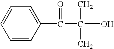
Irgacure 2959 
Darocur MBF 
Irgacure 651 
Iragacure 369 
Darocur TPO 
Irgacure 784 
- Table 4 shows formulas of representative thermal initiators useful in the present invention.
TABLE 4 KIND STRUCTURE BP 
AP 
t-BTP 
CHP 
AIBN 
- FIG. 2 is a cross-sectional view for illustrating a manufacturing method of an organic electroluminescent device according to a second embodiment of the present invention. In this embodiment, an encapsulation film including a
polymer layer 140 and a moisture-absorbinglayer 150 is formed on a laminate structure of an organic electroluminescent device, which will be described in more detail with reference to FIG. 2. In the same manner as shown in FIG. 1, a laminate structure having atransparent electrode 112, ahole injection layer 122, ahole transport layer 124, alight emitting layer 126, anelectron transport layer 128 and ametal electrode 130, is formed onsubstrate 110. Thereafter, the laminate structure is coated with an organic solution containing a vinyl monomer and a polymerization initiator and polymerized to form apolymer layer 140. Thepolymer layer 140 can be formed by the same method as that of forming thepolymer layer 40 shown in FIG. 1, with a proviso that no moisture absorbent is contained in the organic solution for forming thepolymer layer 140 but a separate moisture-absorbinglayer 150 is formed on thepolymer layer 140. The moisture-absorbinglayer 150 is formed for the purpose of absorbing moisture and oxygen in the air, and is made of a material selected from the group consisting of calcium, silica gel, zeolite and alkali metal. - Preferred manufacturing examples of the organic electroluminescent device according to the present invention will now be described in detail.
- In order to form a laminate structure of the organic electroluminescent device shown in FIG. 1, an ITO electrode was formed on a glass substrate, a 30 nm thick 4,4′,4″-tris(N-3(3-methylphenyl)-N-phenylamino)triphenylamine (MTDATA) and a 30 nm thick N,N′-diphenyl-N,N′-bis(3-methylphenyl)-(1,1′-biphenyl)-4,4′-diamine (TPD) were sequentially formed thereon as a hole injection layer and a hole transport layer, respectively. Next, a 60 nm thick Alq 3 layer was vacuum-deposited to form a green light emitting layer. A 1 nm thick LiF layer and a 100 nm thick Al layer were vacuum-deposited on the light emitting layer to form a metal electrode for a cathode.
- A mixed solution of 40 wt % TMPEOTA, 30 wt % TPGDA and 30 wt % epoxy acrylate oligomer (Molecular weight=1000), based on the total weight of the monomer and oligomer, were prepared. Then, 20 wt % HSP188 as a polymerization initiator, based on the total weight of the mixed solution, was mixed with the mixed solution to give an organic solution. The organic solution was spin-coated on the thus-formed laminate structure in the presence of air. Thereafter, light was irradiated into the coated organic solution for polymerization of the organic solution, thereby forming an encapsulation film.
- As described above, the organic solution including a monomer, a polymerization initiator and an oligomer, prepared by wet processing, was brought into direct contact with the laminate structure of the organic electroluminescent device, followed by a series of steps for forming an encapsulation film. However, no change in optical properties of the organic electroluminescent device, e.g., luminance or quantization efficiency, was observed between before and after forming the encapsulation film.
- A change in luminance between the organic electroluminescent device according to Example 1 of the present invention and an organic electroluminescent device (Comparative Example) prepared in the same manner as in Example 1, except that an encapsulation film is not formed, was examined over time while applying a constant bias current of 0.1 mA, and the results thereof are shown in Table 5 and FIG. 3.
TABLE 5 Initial Luminance (cd/m2) Life time (Hr) Comparative Example 104.6 24.7 Example 102.2 110.2 - In Table 5, the term “life time” means a time required until the luminance is reduced to a half the initial luminance. As shown in Table 5, the initial luminances of the devices according to Example and Comparative Example were substantially the same with each other, the organic electroluminescent device prepared in Example of the present invention maintained good luminance characteristics over time, that is, much longer life time than that prepared in Comparative Example, from which it is confirmed that the organic electroluminescent device according to the present invention can be effectively encapsulated by a polymer layer formed by wet processing.
- In Example 1, the process of forming the encapsulation film was performed in the presence of air. However, the encapsulation film forming process can be performed in the presence of inert gas in which oxygen and moisture are maximally reduced. In the case where the encapsulation film is formed in the presence of inert gas, the encapsulation film forming process can be more efficiently performed.
- An organic electroluminescent device was manufactured in the same manner as in Example 1, except that a mixed solution of a TMPEOTA monomer and 20 wt % HSP 188 as a polymerization initiator based on the weight of the monomer, was used as an organic solution in order to evaluate the addition effect of epoxy acrylate oligomer (Molecular weight=1000) added for forming an encapsulation film.
- The organic solution was prepared in the same manner as in Example 1, coated on the laminate structure, and polymerized to form an encapsulation film to give an organic electroluminescent device. The life time of the organic electroluminescent device was evaluated in the same manner as in Example 1. As the result, the life time of the organic electroluminescent device prepared in Example 2 was 44.8 hours even when a bias current is not applied thereto. Also, an oligomer was added to the organic solution when forming the encapsulation film, thereby increasing adhesion to a metal electrode. Compared to an encapsulation film using only a monomer, the encapsulation film prepared in this example had reduced micro-cracks. These properties greatly affected the life time of an organic electroluminescent device.
- An encapsulation film was further formed on the encapsulation film prepared in Example 2, thereby form a bilayered encapsulation film.
- The organic electroluminescent device prepared in Example 3 was evaluated in the same manner as in Example 2, and the life time thereof was 54.3 hours, confirming that the life time of an organic electroluminescent device is dependent upon the thickness of an encapsulation film.
- An organic electroluminescent device was manufactured in the same manner as in Example 2, except that ST was used as a monomer forming an organic solution instead of TMPEOTA and Irgacure 907 was as a polymerization initiator instead of HSP188.
- As a result, no change in optical properties of the organic electroluminescent device, e.g., luminance or quantization efficiency, was observed between before and after forming the encapsulation film.
- In the organic electroluminescent device according to the present invention, in order to form an encapsulation film, an organic solution containing a vinyl monomer and a polymerization initiator was coated on a laminate structure in which an anode, an organic light emitting layer and a cathode are sequentially disposed and a polymerization reaction was induced to the organic solution to form an encapsulation film on the laminate structure.
- According to the present invention, encapsulation film can be manufactured by wet processing in which manufacturability and processing stability are ensured, without separately providing expensive equipment such as a vacuum chamber or a vacuum pump using known, low-cost vinyl monomer and polymerization initiator.
- In the case of using a photo initiator as a polymerization initiator during wet processing for forming a encapsulation film, the encapsulation film can be formed only at a desired location by patterning using a mask by which irradiated light can be selectively shielded.
- Also, when forming an encapsulation film by wet processing, in order to further extend the life time of an organic electroluminescent device, an oligomer is added in forming an encapsulation film rather than using vinyl monomer only, thereby increasing adhesion and hardness of the encapsulation film and enhancing the denseness of an encapsulation film surface. As a result, the life time of an organic electroluminescent device can be greatly extended.
- Further, when forming an encapsulation film by wet processing, a moisture absorbent for absorbing moisture and oxygen from the air may be added to an organic solution for forming an encapsulation film, thereby forming a hybrid encapsulation film. Alternatively, a separate moisture-absorbing layer may be formed on a polymer layer formed by wet processing, thereby extending the life time of an organic electroluminescent device.
- The encapsulation film according to the present invention formed by wet processing can be easily applied to fabrication of a large-screen display panel and flexible displays.
- While the present invention has been particularly shown and described with reference to preferred embodiments thereof, it will be understood by those of ordinary skill in the art that various changes in form and details may be made therein without departing from the spirit and scope of the present invention as defined by the following claims.
Claims (22)
Applications Claiming Priority (2)
| Application Number | Priority Date | Filing Date | Title |
|---|---|---|---|
| KR10-2002-0020908A KR100475849B1 (en) | 2002-04-17 | 2002-04-17 | Organic electroluminescent devices having encapsulation thin film formed by wet processing and methods for manufacturing the same |
| KR2002-20908 | 2002-04-17 |
Publications (2)
| Publication Number | Publication Date |
|---|---|
| US20030198830A1 true US20030198830A1 (en) | 2003-10-23 |
| US7005199B2 US7005199B2 (en) | 2006-02-28 |
Family
ID=29208712
Family Applications (1)
| Application Number | Title | Priority Date | Filing Date |
|---|---|---|---|
| US10/392,131 Expired - Lifetime US7005199B2 (en) | 2002-04-17 | 2003-03-18 | Organic electroluminescent devices having encapsulation thin film formed by wet processing and methods for manufacturing the same |
Country Status (2)
| Country | Link |
|---|---|
| US (1) | US7005199B2 (en) |
| KR (1) | KR100475849B1 (en) |
Cited By (14)
| Publication number | Priority date | Publication date | Assignee | Title |
|---|---|---|---|---|
| US20060138946A1 (en) * | 2004-12-29 | 2006-06-29 | Jian Wang | Electrical device with a low reflectivity layer |
| EP1712109A1 (en) * | 2003-12-30 | 2006-10-18 | Agency for Science, Technology and Research | Flexible electroluminescent devices |
| US20080305350A1 (en) * | 2007-02-15 | 2008-12-11 | Yuya Agata | Barrier laminate, barrier film substrate, methods for producing them, and device |
| EP2235131A2 (en) * | 2007-12-28 | 2010-10-06 | 3M Innovative Properties Company | Flexible encapsulating film systems |
| US20100270582A1 (en) * | 2009-04-22 | 2010-10-28 | Shat-R-Shiel, Inc. | Coated light-emitting diode |
| US20100283386A1 (en) * | 2008-01-11 | 2010-11-11 | Sony Corporation | Display device and composition for producing display device, and display device |
| US20110210364A1 (en) * | 2009-04-22 | 2011-09-01 | Shat-R-Shield, Inc. | Silicone coated light-emitting diode |
| US8319423B2 (en) * | 2006-10-24 | 2012-11-27 | Lg Display Co., Ltd. | Display device with protecting layer for getter layer |
| EP2629590A1 (en) * | 2008-06-17 | 2013-08-21 | Hitachi Ltd. | An organic light-emitting device |
| US20140306600A1 (en) * | 2013-04-16 | 2014-10-16 | Samsung Display Co., Ltd. | Deposition mask, method of manufacturing display apparatus by using the deposition mask, and display apparatus manufactured by the method |
| US20180158879A1 (en) * | 2015-06-19 | 2018-06-07 | Samsung Sdi Co., Ltd. | Organic light emitting display |
| CN109904345A (en) * | 2019-02-28 | 2019-06-18 | 武汉华星光电半导体显示技术有限公司 | Encapsulating structure and its display device |
| CN110710012A (en) * | 2017-06-09 | 2020-01-17 | 株式会社Lg化学 | Packaging film |
| US10700133B2 (en) | 2015-06-19 | 2020-06-30 | Samsung Sdi Co., Ltd. | Organic light emitting display |
Families Citing this family (7)
| Publication number | Priority date | Publication date | Assignee | Title |
|---|---|---|---|---|
| KR100554161B1 (en) * | 2002-11-29 | 2006-02-22 | 한국전자통신연구원 | Encapsulation thin film materials obtained from tetraoxaspiro or dioxane monomer and encapsulation methods using the same |
| KR100993827B1 (en) * | 2003-12-01 | 2010-11-12 | 삼성전자주식회사 | Light emitting device and display device having the same and method of manufacturing thereof |
| KR100682963B1 (en) * | 2006-02-03 | 2007-02-15 | 삼성전자주식회사 | Organic light emitting display providing ultraviolet protecting film |
| DE102009023350A1 (en) | 2009-05-29 | 2010-12-02 | Osram Opto Semiconductors Gmbh | Electronic component and method for producing an electronic component |
| US9909022B2 (en) | 2014-07-25 | 2018-03-06 | Kateeva, Inc. | Organic thin film ink compositions and methods |
| WO2017039857A1 (en) | 2015-08-31 | 2017-03-09 | Kateeva, Inc. | Di- and mono(meth)acrylate based organic thin film ink compositions |
| JP7144864B2 (en) | 2017-04-21 | 2022-09-30 | カティーバ, インコーポレイテッド | Compositions and techniques for forming organic thin films |
Citations (22)
| Publication number | Priority date | Publication date | Assignee | Title |
|---|---|---|---|---|
| US5395644A (en) * | 1992-08-21 | 1995-03-07 | Battelle Memorial Institute | Vacuum deposition and curing of liquid monomers |
| US5414293A (en) * | 1992-10-14 | 1995-05-09 | International Business Machines Corporation | Encapsulated light emitting diodes |
| US5427858A (en) * | 1990-11-30 | 1995-06-27 | Idemitsu Kosan Company Limited | Organic electroluminescence device with a fluorine polymer layer |
| US5734225A (en) * | 1996-07-10 | 1998-03-31 | International Business Machines Corporation | Encapsulation of organic light emitting devices using siloxane or siloxane derivatives |
| US5855994A (en) * | 1996-07-10 | 1999-01-05 | International Business Machines Corporation | Siloxane and siloxane derivatives as encapsulants for organic light emitting devices |
| US5902641A (en) * | 1997-09-29 | 1999-05-11 | Battelle Memorial Institute | Flash evaporation of liquid monomer particle mixture |
| US5952778A (en) * | 1997-03-18 | 1999-09-14 | International Business Machines Corporation | Encapsulated organic light emitting device |
| US6146225A (en) * | 1998-07-30 | 2000-11-14 | Agilent Technologies, Inc. | Transparent, flexible permeability barrier for organic electroluminescent devices |
| US6203854B1 (en) * | 1997-09-17 | 2001-03-20 | Brent International Plc | Methods of and compositions for preventing corrosion of metal substrates |
| US6207239B1 (en) * | 1998-12-16 | 2001-03-27 | Battelle Memorial Institute | Plasma enhanced chemical deposition of conjugated polymer |
| US6217947B1 (en) * | 1998-12-16 | 2001-04-17 | Battelle Memorial Institute | Plasma enhanced polymer deposition onto fixtures |
| US6224948B1 (en) * | 1997-09-29 | 2001-05-01 | Battelle Memorial Institute | Plasma enhanced chemical deposition with low vapor pressure compounds |
| US6228436B1 (en) * | 1998-12-16 | 2001-05-08 | Battelle Memorial Institute | Method of making light emitting polymer composite material |
| US6268695B1 (en) * | 1998-12-16 | 2001-07-31 | Battelle Memorial Institute | Environmental barrier material for organic light emitting device and method of making |
| US20020096995A1 (en) * | 2000-11-16 | 2002-07-25 | Fuji Photo Film Co., Ltd. | Light-emitting device |
| US20030062186A1 (en) * | 2001-09-21 | 2003-04-03 | Eastman Kodak Company | Sealing structure for highly moisture-sensitive electronic device element and method for fabrication |
| US20030143423A1 (en) * | 2002-01-31 | 2003-07-31 | 3M Innovative Properties Company | Encapsulation of organic electronic devices using adsorbent loaded adhesives |
| US20030184221A1 (en) * | 2002-03-28 | 2003-10-02 | Masayuki Mishima | Light-emitting device |
| US20030209979A1 (en) * | 2002-05-07 | 2003-11-13 | Osram Opto Semiconductors Gmbh | Encapsulation for electroluminescent devices |
| US20040024105A1 (en) * | 2002-08-01 | 2004-02-05 | Kim Gi Heon | Thin film material using pentaerythritol acrylate for encapsulation of organic or polymeric light emitting device, and encapsulation method for LED using the same |
| US20040119403A1 (en) * | 2002-12-19 | 2004-06-24 | 3M Innovative Properties Company | Organic electroluminescent device and encapsulation method |
| US6872473B2 (en) * | 2001-07-20 | 2005-03-29 | Lg Electronics Inc. | Panel display device and method for forming protective layer within the same |
Family Cites Families (5)
| Publication number | Priority date | Publication date | Assignee | Title |
|---|---|---|---|---|
| JPH0433292A (en) * | 1990-05-29 | 1992-02-04 | Iwasaki Electric Co Ltd | El light emitting element |
| JPH06215872A (en) * | 1993-01-19 | 1994-08-05 | Nippon Kasei Chem Co Ltd | Organic dispersion type el element |
| KR100215768B1 (en) * | 1997-06-14 | 1999-08-16 | 구자홍 | Organic Electroluminescence Device |
| KR100595167B1 (en) * | 1999-03-12 | 2006-07-03 | 엘지전자 주식회사 | organic electroluminescence device with organic coating layer for preventing penetration of moisture |
| DE19920799A1 (en) * | 1999-05-06 | 2000-11-16 | Basf Coatings Ag | Coating material curable thermally and with actinic radiation and its use |
-
2002
- 2002-04-17 KR KR10-2002-0020908A patent/KR100475849B1/en not_active IP Right Cessation
-
2003
- 2003-03-18 US US10/392,131 patent/US7005199B2/en not_active Expired - Lifetime
Patent Citations (24)
| Publication number | Priority date | Publication date | Assignee | Title |
|---|---|---|---|---|
| US5427858A (en) * | 1990-11-30 | 1995-06-27 | Idemitsu Kosan Company Limited | Organic electroluminescence device with a fluorine polymer layer |
| US5547508A (en) * | 1992-08-21 | 1996-08-20 | Battelle Memorial Institute | Vacuum deposition and curing of liquid monomers apparatus |
| US5395644A (en) * | 1992-08-21 | 1995-03-07 | Battelle Memorial Institute | Vacuum deposition and curing of liquid monomers |
| US5414293A (en) * | 1992-10-14 | 1995-05-09 | International Business Machines Corporation | Encapsulated light emitting diodes |
| US5734225A (en) * | 1996-07-10 | 1998-03-31 | International Business Machines Corporation | Encapsulation of organic light emitting devices using siloxane or siloxane derivatives |
| US5855994A (en) * | 1996-07-10 | 1999-01-05 | International Business Machines Corporation | Siloxane and siloxane derivatives as encapsulants for organic light emitting devices |
| US5952778A (en) * | 1997-03-18 | 1999-09-14 | International Business Machines Corporation | Encapsulated organic light emitting device |
| US6203854B1 (en) * | 1997-09-17 | 2001-03-20 | Brent International Plc | Methods of and compositions for preventing corrosion of metal substrates |
| US6224948B1 (en) * | 1997-09-29 | 2001-05-01 | Battelle Memorial Institute | Plasma enhanced chemical deposition with low vapor pressure compounds |
| US5902641A (en) * | 1997-09-29 | 1999-05-11 | Battelle Memorial Institute | Flash evaporation of liquid monomer particle mixture |
| US6146225A (en) * | 1998-07-30 | 2000-11-14 | Agilent Technologies, Inc. | Transparent, flexible permeability barrier for organic electroluminescent devices |
| US6207239B1 (en) * | 1998-12-16 | 2001-03-27 | Battelle Memorial Institute | Plasma enhanced chemical deposition of conjugated polymer |
| US6217947B1 (en) * | 1998-12-16 | 2001-04-17 | Battelle Memorial Institute | Plasma enhanced polymer deposition onto fixtures |
| US6228436B1 (en) * | 1998-12-16 | 2001-05-08 | Battelle Memorial Institute | Method of making light emitting polymer composite material |
| US6268695B1 (en) * | 1998-12-16 | 2001-07-31 | Battelle Memorial Institute | Environmental barrier material for organic light emitting device and method of making |
| US20020096995A1 (en) * | 2000-11-16 | 2002-07-25 | Fuji Photo Film Co., Ltd. | Light-emitting device |
| US6872473B2 (en) * | 2001-07-20 | 2005-03-29 | Lg Electronics Inc. | Panel display device and method for forming protective layer within the same |
| US20030062186A1 (en) * | 2001-09-21 | 2003-04-03 | Eastman Kodak Company | Sealing structure for highly moisture-sensitive electronic device element and method for fabrication |
| US6590157B2 (en) * | 2001-09-21 | 2003-07-08 | Eastman Kodak Company | Sealing structure for highly moisture-sensitive electronic device element and method for fabrication |
| US20030143423A1 (en) * | 2002-01-31 | 2003-07-31 | 3M Innovative Properties Company | Encapsulation of organic electronic devices using adsorbent loaded adhesives |
| US20030184221A1 (en) * | 2002-03-28 | 2003-10-02 | Masayuki Mishima | Light-emitting device |
| US20030209979A1 (en) * | 2002-05-07 | 2003-11-13 | Osram Opto Semiconductors Gmbh | Encapsulation for electroluminescent devices |
| US20040024105A1 (en) * | 2002-08-01 | 2004-02-05 | Kim Gi Heon | Thin film material using pentaerythritol acrylate for encapsulation of organic or polymeric light emitting device, and encapsulation method for LED using the same |
| US20040119403A1 (en) * | 2002-12-19 | 2004-06-24 | 3M Innovative Properties Company | Organic electroluminescent device and encapsulation method |
Cited By (26)
| Publication number | Priority date | Publication date | Assignee | Title |
|---|---|---|---|---|
| EP1712109A4 (en) * | 2003-12-30 | 2008-03-19 | Agency Science Tech & Res | Flexible electroluminescent devices |
| EP1712109A1 (en) * | 2003-12-30 | 2006-10-18 | Agency for Science, Technology and Research | Flexible electroluminescent devices |
| US20070222370A1 (en) * | 2003-12-30 | 2007-09-27 | Agency For Science, Technology And Research | Flexible Electroluminescent Devices |
| US20060138946A1 (en) * | 2004-12-29 | 2006-06-29 | Jian Wang | Electrical device with a low reflectivity layer |
| US8319423B2 (en) * | 2006-10-24 | 2012-11-27 | Lg Display Co., Ltd. | Display device with protecting layer for getter layer |
| US20080305350A1 (en) * | 2007-02-15 | 2008-12-11 | Yuya Agata | Barrier laminate, barrier film substrate, methods for producing them, and device |
| US8197946B2 (en) * | 2007-02-15 | 2012-06-12 | Fujifilm Corporation | Barrier laminate, barrier film substrate, methods for producing them, and device |
| EP2235131A2 (en) * | 2007-12-28 | 2010-10-06 | 3M Innovative Properties Company | Flexible encapsulating film systems |
| US20100272933A1 (en) * | 2007-12-28 | 2010-10-28 | Mccormick Fred B | Flexible encapsulating film systems |
| US8846169B2 (en) | 2007-12-28 | 2014-09-30 | 3M Innovative Properties Company | Flexible encapsulating film systems |
| EP2235131A4 (en) * | 2007-12-28 | 2013-10-02 | 3M Innovative Properties Co | Flexible encapsulating film systems |
| US20100283386A1 (en) * | 2008-01-11 | 2010-11-11 | Sony Corporation | Display device and composition for producing display device, and display device |
| US8536611B2 (en) | 2008-06-17 | 2013-09-17 | Hitachi, Ltd. | Organic light-emitting element, method for manufacturing the organic light-emitting element, apparatus for manufacturing the organic light-emitting element, and organic light-emitting device using the organic light-emitting element |
| EP2629590A1 (en) * | 2008-06-17 | 2013-08-21 | Hitachi Ltd. | An organic light-emitting device |
| US20100270582A1 (en) * | 2009-04-22 | 2010-10-28 | Shat-R-Shiel, Inc. | Coated light-emitting diode |
| US20110210364A1 (en) * | 2009-04-22 | 2011-09-01 | Shat-R-Shield, Inc. | Silicone coated light-emitting diode |
| US8697458B2 (en) | 2009-04-22 | 2014-04-15 | Shat-R-Shield, Inc. | Silicone coated light-emitting diode |
| US20100270574A1 (en) * | 2009-04-22 | 2010-10-28 | Shat-R-Shield, Inc. | Silicone coated light-emitting diode |
| US9236536B2 (en) | 2009-04-22 | 2016-01-12 | Shat-R-Shield, Inc. | Silicone coated light-emitting diode |
| US20140306600A1 (en) * | 2013-04-16 | 2014-10-16 | Samsung Display Co., Ltd. | Deposition mask, method of manufacturing display apparatus by using the deposition mask, and display apparatus manufactured by the method |
| US9166166B2 (en) * | 2013-04-16 | 2015-10-20 | Samsung Display Co., Ltd. | Deposition mask, method of manufacturing display apparatus by using the deposition mask, and display apparatus manufactured by the method |
| US20180158879A1 (en) * | 2015-06-19 | 2018-06-07 | Samsung Sdi Co., Ltd. | Organic light emitting display |
| US10700133B2 (en) | 2015-06-19 | 2020-06-30 | Samsung Sdi Co., Ltd. | Organic light emitting display |
| US10756139B2 (en) * | 2015-06-19 | 2020-08-25 | Samsung Sdi Co., Ltd. | Organic light emitting display |
| CN110710012A (en) * | 2017-06-09 | 2020-01-17 | 株式会社Lg化学 | Packaging film |
| CN109904345A (en) * | 2019-02-28 | 2019-06-18 | 武汉华星光电半导体显示技术有限公司 | Encapsulating structure and its display device |
Also Published As
| Publication number | Publication date |
|---|---|
| KR20030082257A (en) | 2003-10-22 |
| US7005199B2 (en) | 2006-02-28 |
| KR100475849B1 (en) | 2005-03-10 |
Similar Documents
| Publication | Publication Date | Title |
|---|---|---|
| US7005199B2 (en) | Organic electroluminescent devices having encapsulation thin film formed by wet processing and methods for manufacturing the same | |
| KR101871549B1 (en) | Sealant composition for display, organic protective layer comprising the same, and display apparatus comprising the same | |
| CN1201416C (en) | Plate display and its protecting layer forming process | |
| KR101943687B1 (en) | Organic light emmiting diode display apparatus | |
| CN1498048B (en) | Organic electroluminescence device | |
| EP3023444B1 (en) | Composition for fabricating organic film, organic light-emitting display apparatus manufactured using the same, and method of manufacturing the organic light-emitting display apparatus | |
| US20080114117A1 (en) | Thin film material using pentaerythritol acrylate for encapsulation of organic or polymeric light emitting device, and encapsulation method for LED using the same | |
| KR102072799B1 (en) | Organic light emitting device and method for preparing the same | |
| KR101943688B1 (en) | Organic light emmiting diode display apparatus | |
| US20150252125A1 (en) | Curable resin compositions and barrier stacks including the same | |
| US9490454B2 (en) | Method for producing a high efficiency organic light emitting device having a transparent composite electrode comprising a film of conductive nanowires, carbon nanoparticles, light scattering nanoparticles, and a polymer support | |
| KR101943689B1 (en) | Organic light emmiting diode display apparatus | |
| US20140264317A1 (en) | Organic electroluminescence element and planar light-emitting body | |
| JP7253542B2 (en) | Sealant for organic electroluminescence display elements | |
| KR20180102038A (en) | Photo-curable composition, organic protective layer comprising the same, and apparatus comprising the same | |
| WO2022039019A1 (en) | Composition for electronic device sealing, method for forming electronic device sealing film, and electronic device sealing film | |
| JP7090121B2 (en) | Composition for encapsulating an organic light emitting device and an organic light emitting display device manufactured from the composition. | |
| JP2007311219A (en) | Organic electroluminescent element | |
| KR20030089749A (en) | Organic electroluminescent devices having encapsulation thin film comprising polyamide and methods for manufacturing the same | |
| CN116789896A (en) | Composition, cured product, sealing material for organic electroluminescent display element, and organic electroluminescent display device | |
| US20230124280A1 (en) | Encapsulation material for light-emitting element and light-emitting device manufactured using the same | |
| KR102580276B1 (en) | Compound, photocurable composition, cured film, and organic electro luminescence element | |
| KR100503828B1 (en) | Thin Film Material using Pentaerithritol acrylate for Encapsulation of Organic or Polymeric Electronic Light Emitting Device, and Encapsulation Method for LED | |
| JP2011258383A (en) | Organic el element and display device using the same | |
| CN1474634A (en) | Organic electrically execiting light-emitting device |
Legal Events
| Date | Code | Title | Description |
|---|---|---|---|
| AS | Assignment |
Owner name: ELECTRONICS AND TELECOMMUNICATIONS RESEARCH INSTIT Free format text: ASSIGNMENT OF ASSIGNORS INTEREST;ASSIGNORS:KIM, GI-HEON;OH, JI-YOUNG;CHU, HYE-YONG;AND OTHERS;REEL/FRAME:013894/0633 Effective date: 20030106 |
|
| FEPP | Fee payment procedure |
Free format text: PAYOR NUMBER ASSIGNED (ORIGINAL EVENT CODE: ASPN); ENTITY STATUS OF PATENT OWNER: SMALL ENTITY |
|
| STCF | Information on status: patent grant |
Free format text: PATENTED CASE |
|
| FEPP | Fee payment procedure |
Free format text: PAYOR NUMBER ASSIGNED (ORIGINAL EVENT CODE: ASPN); ENTITY STATUS OF PATENT OWNER: SMALL ENTITY Free format text: PAYER NUMBER DE-ASSIGNED (ORIGINAL EVENT CODE: RMPN); ENTITY STATUS OF PATENT OWNER: SMALL ENTITY |
|
| FPAY | Fee payment |
Year of fee payment: 4 |
|
| AS | Assignment |
Owner name: IPG ELECTRONICS 502 LIMITED Free format text: ASSIGNMENT OF ONE HALF (1/2) OF ALL OF ASSIGNORS' RIGHT, TITLE AND INTEREST;ASSIGNOR:ELECTRONICS AND TELECOMMUNICATIONS RESEARCH INSTITUTE;REEL/FRAME:023456/0363 Effective date: 20081226 |
|
| FEPP | Fee payment procedure |
Free format text: PAT HOLDER NO LONGER CLAIMS SMALL ENTITY STATUS, ENTITY STATUS SET TO UNDISCOUNTED (ORIGINAL EVENT CODE: STOL); ENTITY STATUS OF PATENT OWNER: SMALL ENTITY |
|
| AS | Assignment |
Owner name: ELECTRONICS AND TELECOMMUNICATIONS RESEARCH INSTIT Free format text: ASSIGNMENT OF ASSIGNORS INTEREST;ASSIGNOR:IPG ELECTRONICS 502 LIMITED;REEL/FRAME:029134/0699 Effective date: 20120723 |
|
| FEPP | Fee payment procedure |
Free format text: PAYER NUMBER DE-ASSIGNED (ORIGINAL EVENT CODE: RMPN); ENTITY STATUS OF PATENT OWNER: SMALL ENTITY Free format text: PAYOR NUMBER ASSIGNED (ORIGINAL EVENT CODE: ASPN); ENTITY STATUS OF PATENT OWNER: SMALL ENTITY |
|
| FEPP | Fee payment procedure |
Free format text: PAT HOLDER CLAIMS SMALL ENTITY STATUS, ENTITY STATUS SET TO SMALL (ORIGINAL EVENT CODE: LTOS); ENTITY STATUS OF PATENT OWNER: SMALL ENTITY |
|
| FPAY | Fee payment |
Year of fee payment: 8 |
|
| AS | Assignment |
Owner name: INTELLECTUAL DISCOVERY CO. LTD., KOREA, REPUBLIC O Free format text: ASSIGNMENT OF ASSIGNORS INTEREST;ASSIGNOR:ELECTRONICS AND TELECOMMUNICATIONS RESEARCH INSTITUTE;REEL/FRAME:030418/0587 Effective date: 20130508 |
|
| FEPP | Fee payment procedure |
Free format text: PAYER NUMBER DE-ASSIGNED (ORIGINAL EVENT CODE: RMPN); ENTITY STATUS OF PATENT OWNER: SMALL ENTITY Free format text: PAYOR NUMBER ASSIGNED (ORIGINAL EVENT CODE: ASPN); ENTITY STATUS OF PATENT OWNER: SMALL ENTITY |
|
| FPAY | Fee payment |
Year of fee payment: 12 |