US20030231851A1 - Hydrophobic materials for waveguides, optical devices, and other applications - Google Patents
Hydrophobic materials for waveguides, optical devices, and other applications Download PDFInfo
- Publication number
- US20030231851A1 US20030231851A1 US10/150,859 US15085902A US2003231851A1 US 20030231851 A1 US20030231851 A1 US 20030231851A1 US 15085902 A US15085902 A US 15085902A US 2003231851 A1 US2003231851 A1 US 2003231851A1
- Authority
- US
- United States
- Prior art keywords
- waveguide
- hydrophobic layer
- hydrophobic
- less
- layer material
- Prior art date
- Legal status (The legal status is an assumption and is not a legal conclusion. Google has not performed a legal analysis and makes no representation as to the accuracy of the status listed.)
- Granted
Links
- 239000000463 material Substances 0.000 title claims abstract description 261
- 230000002209 hydrophobic effect Effects 0.000 title claims abstract description 178
- 230000003287 optical effect Effects 0.000 title claims abstract description 71
- 238000000034 method Methods 0.000 claims abstract description 293
- 239000010410 layer Substances 0.000 claims abstract description 282
- 239000000758 substrate Substances 0.000 claims abstract description 103
- 238000005253 cladding Methods 0.000 claims abstract description 94
- XLYOFNOQVPJJNP-UHFFFAOYSA-N water Substances O XLYOFNOQVPJJNP-UHFFFAOYSA-N 0.000 claims abstract description 56
- 239000012792 core layer Substances 0.000 claims abstract description 51
- 238000002161 passivation Methods 0.000 claims abstract description 8
- 125000000962 organic group Chemical group 0.000 claims description 65
- 125000000217 alkyl group Chemical group 0.000 claims description 61
- 125000003118 aryl group Chemical group 0.000 claims description 59
- 125000003342 alkenyl group Chemical group 0.000 claims description 48
- 238000000151 deposition Methods 0.000 claims description 41
- 239000002904 solvent Substances 0.000 claims description 38
- 125000001424 substituent group Chemical group 0.000 claims description 32
- 229910052710 silicon Inorganic materials 0.000 claims description 31
- WYURNTSHIVDZCO-UHFFFAOYSA-N Tetrahydrofuran Chemical compound C1CCOC1 WYURNTSHIVDZCO-UHFFFAOYSA-N 0.000 claims description 27
- 230000008021 deposition Effects 0.000 claims description 27
- XUIMIQQOPSSXEZ-UHFFFAOYSA-N Silicon Chemical compound [Si] XUIMIQQOPSSXEZ-UHFFFAOYSA-N 0.000 claims description 24
- 238000004132 cross linking Methods 0.000 claims description 23
- 239000010703 silicon Substances 0.000 claims description 23
- 230000010287 polarization Effects 0.000 claims description 22
- LFQSCWFLJHTTHZ-UHFFFAOYSA-N Ethanol Chemical compound CCO LFQSCWFLJHTTHZ-UHFFFAOYSA-N 0.000 claims description 20
- 239000002019 doping agent Substances 0.000 claims description 20
- 239000011162 core material Substances 0.000 claims description 19
- 239000000835 fiber Substances 0.000 claims description 19
- 230000001419 dependent effect Effects 0.000 claims description 17
- KFZMGEQAYNKOFK-UHFFFAOYSA-N Isopropanol Chemical group CC(C)O KFZMGEQAYNKOFK-UHFFFAOYSA-N 0.000 claims description 15
- 229910052732 germanium Inorganic materials 0.000 claims description 15
- 125000001997 phenyl group Chemical group [H]C1=C([H])C([H])=C(*)C([H])=C1[H] 0.000 claims description 15
- VYPSYNLAJGMNEJ-UHFFFAOYSA-N silicon dioxide Inorganic materials O=[Si]=O VYPSYNLAJGMNEJ-UHFFFAOYSA-N 0.000 claims description 14
- 230000009477 glass transition Effects 0.000 claims description 13
- 125000005647 linker group Chemical group 0.000 claims description 13
- OKKJLVBELUTLKV-UHFFFAOYSA-N Methanol Chemical compound OC OKKJLVBELUTLKV-UHFFFAOYSA-N 0.000 claims description 12
- 229910052796 boron Inorganic materials 0.000 claims description 11
- 239000011521 glass Substances 0.000 claims description 11
- 239000000872 buffer Substances 0.000 claims description 10
- 229910052739 hydrogen Inorganic materials 0.000 claims description 10
- 239000010453 quartz Substances 0.000 claims description 10
- 239000004065 semiconductor Substances 0.000 claims description 10
- 230000003746 surface roughness Effects 0.000 claims description 10
- NTIZESTWPVYFNL-UHFFFAOYSA-N Methyl isobutyl ketone Chemical compound CC(C)CC(C)=O NTIZESTWPVYFNL-UHFFFAOYSA-N 0.000 claims description 9
- UIHCLUNTQKBZGK-UHFFFAOYSA-N Methyl isobutyl ketone Natural products CCC(C)C(C)=O UIHCLUNTQKBZGK-UHFFFAOYSA-N 0.000 claims description 9
- YXFVVABEGXRONW-UHFFFAOYSA-N Toluene Chemical compound CC1=CC=CC=C1 YXFVVABEGXRONW-UHFFFAOYSA-N 0.000 claims description 9
- 229910052782 aluminium Inorganic materials 0.000 claims description 8
- JHIVVAPYMSGYDF-UHFFFAOYSA-N cyclohexanone Chemical compound O=C1CCCCC1 JHIVVAPYMSGYDF-UHFFFAOYSA-N 0.000 claims description 8
- 239000003999 initiator Substances 0.000 claims description 8
- 229910052752 metalloid Inorganic materials 0.000 claims description 8
- 150000002738 metalloids Chemical class 0.000 claims description 8
- 229910052715 tantalum Inorganic materials 0.000 claims description 8
- 229910052719 titanium Inorganic materials 0.000 claims description 8
- 239000010936 titanium Substances 0.000 claims description 8
- 229910052723 transition metal Inorganic materials 0.000 claims description 8
- 150000003624 transition metals Chemical class 0.000 claims description 8
- 229910052726 zirconium Inorganic materials 0.000 claims description 8
- QVGXLLKOCUKJST-UHFFFAOYSA-N atomic oxygen Chemical compound [O] QVGXLLKOCUKJST-UHFFFAOYSA-N 0.000 claims description 7
- GNPVGFCGXDBREM-UHFFFAOYSA-N germanium atom Chemical compound [Ge] GNPVGFCGXDBREM-UHFFFAOYSA-N 0.000 claims description 7
- 229910052760 oxygen Inorganic materials 0.000 claims description 7
- 239000001301 oxygen Substances 0.000 claims description 7
- 239000004033 plastic Substances 0.000 claims description 7
- 229920003023 plastic Polymers 0.000 claims description 7
- 238000012876 topography Methods 0.000 claims description 7
- 230000005670 electromagnetic radiation Effects 0.000 claims description 6
- 229910010272 inorganic material Inorganic materials 0.000 claims description 6
- 239000011147 inorganic material Substances 0.000 claims description 6
- 125000002496 methyl group Chemical group [H]C([H])([H])* 0.000 claims description 6
- 238000000059 patterning Methods 0.000 claims description 6
- 238000009987 spinning Methods 0.000 claims description 6
- 238000005507 spraying Methods 0.000 claims description 6
- 229910052718 tin Inorganic materials 0.000 claims description 6
- 229910052691 Erbium Inorganic materials 0.000 claims description 5
- 229910052787 antimony Inorganic materials 0.000 claims description 5
- 238000010894 electron beam technology Methods 0.000 claims description 5
- 125000001495 ethyl group Chemical group [H]C([H])([H])C([H])([H])* 0.000 claims description 5
- 229910052745 lead Inorganic materials 0.000 claims description 5
- 239000000126 substance Substances 0.000 claims description 5
- RYHBNJHYFVUHQT-UHFFFAOYSA-N 1,4-Dioxane Chemical compound C1COCCO1 RYHBNJHYFVUHQT-UHFFFAOYSA-N 0.000 claims description 4
- 229910052769 Ytterbium Inorganic materials 0.000 claims description 4
- 238000010521 absorption reaction Methods 0.000 claims description 4
- 230000008859 change Effects 0.000 claims description 4
- BGTOWKSIORTVQH-UHFFFAOYSA-N cyclopentanone Chemical compound O=C1CCCC1 BGTOWKSIORTVQH-UHFFFAOYSA-N 0.000 claims description 4
- 238000003618 dip coating Methods 0.000 claims description 4
- 229910052751 metal Inorganic materials 0.000 claims description 4
- 239000002184 metal Substances 0.000 claims description 4
- ZOXJGFHDIHLPTG-UHFFFAOYSA-N Boron Chemical group [B] ZOXJGFHDIHLPTG-UHFFFAOYSA-N 0.000 claims description 3
- RTAQQCXQSZGOHL-UHFFFAOYSA-N Titanium Chemical compound [Ti] RTAQQCXQSZGOHL-UHFFFAOYSA-N 0.000 claims description 3
- QCWXUUIWCKQGHC-UHFFFAOYSA-N Zirconium Chemical compound [Zr] QCWXUUIWCKQGHC-UHFFFAOYSA-N 0.000 claims description 3
- 230000015572 biosynthetic process Effects 0.000 claims description 3
- 239000000919 ceramic Substances 0.000 claims description 3
- KPUWHANPEXNPJT-UHFFFAOYSA-N disiloxane Chemical class [SiH3]O[SiH3] KPUWHANPEXNPJT-UHFFFAOYSA-N 0.000 claims description 3
- 239000004973 liquid crystal related substance Substances 0.000 claims description 3
- AUHZEENZYGFFBQ-UHFFFAOYSA-N mesitylene Substances CC1=CC(C)=CC(C)=C1 AUHZEENZYGFFBQ-UHFFFAOYSA-N 0.000 claims description 3
- 125000001827 mesitylenyl group Chemical group [H]C1=C(C(*)=C(C([H])=C1C([H])([H])[H])C([H])([H])[H])C([H])([H])[H] 0.000 claims description 3
- 239000010980 sapphire Substances 0.000 claims description 3
- 229910052594 sapphire Inorganic materials 0.000 claims description 3
- 238000004528 spin coating Methods 0.000 claims description 3
- 238000000137 annealing Methods 0.000 claims description 2
- 239000006185 dispersion Substances 0.000 claims description 2
- 238000002156 mixing Methods 0.000 claims description 2
- 150000003613 toluenes Chemical class 0.000 claims description 2
- 239000011159 matrix material Substances 0.000 claims 3
- UYAHIZSMUZPPFV-UHFFFAOYSA-N erbium Chemical group [Er] UYAHIZSMUZPPFV-UHFFFAOYSA-N 0.000 claims 2
- 150000004706 metal oxides Chemical group 0.000 claims 2
- 229910052758 niobium Inorganic materials 0.000 claims 2
- GUVRBAGPIYLISA-UHFFFAOYSA-N tantalum atom Chemical group [Ta] GUVRBAGPIYLISA-UHFFFAOYSA-N 0.000 claims 2
- 125000006527 (C1-C5) alkyl group Chemical group 0.000 claims 1
- 238000010884 ion-beam technique Methods 0.000 claims 1
- 150000002739 metals Chemical class 0.000 claims 1
- 238000006116 polymerization reaction Methods 0.000 claims 1
- 150000003254 radicals Chemical class 0.000 claims 1
- 238000000576 coating method Methods 0.000 abstract description 10
- 230000008901 benefit Effects 0.000 abstract description 3
- 239000003989 dielectric material Substances 0.000 abstract description 3
- 150000001875 compounds Chemical class 0.000 description 144
- RTZKZFJDLAIYFH-UHFFFAOYSA-N Diethyl ether Chemical compound CCOCC RTZKZFJDLAIYFH-UHFFFAOYSA-N 0.000 description 108
- FYSNRJHAOHDILO-UHFFFAOYSA-N thionyl chloride Chemical compound ClS(Cl)=O FYSNRJHAOHDILO-UHFFFAOYSA-N 0.000 description 98
- 239000000243 solution Substances 0.000 description 70
- IMNFDUFMRHMDMM-UHFFFAOYSA-N N-Heptane Chemical compound CCCCCCC IMNFDUFMRHMDMM-UHFFFAOYSA-N 0.000 description 39
- 125000003545 alkoxy group Chemical group 0.000 description 39
- 125000000304 alkynyl group Chemical group 0.000 description 38
- 230000000737 periodic effect Effects 0.000 description 33
- 229910052736 halogen Inorganic materials 0.000 description 32
- 150000002367 halogens Chemical class 0.000 description 32
- 238000006243 chemical reaction Methods 0.000 description 31
- 239000000460 chlorine Substances 0.000 description 31
- 239000007858 starting material Substances 0.000 description 31
- 229910006124 SOCl2 Inorganic materials 0.000 description 28
- 229960004132 diethyl ether Drugs 0.000 description 26
- 238000006460 hydrolysis reaction Methods 0.000 description 26
- OBTZDIRUQWFRFZ-UHFFFAOYSA-N 2-(5-methylfuran-2-yl)-n-(4-methylphenyl)quinoline-4-carboxamide Chemical compound O1C(C)=CC=C1C1=CC(C(=O)NC=2C=CC(C)=CC=2)=C(C=CC=C2)C2=N1 OBTZDIRUQWFRFZ-UHFFFAOYSA-N 0.000 description 25
- 230000007062 hydrolysis Effects 0.000 description 25
- BOTDANWDWHJENH-UHFFFAOYSA-N Tetraethyl orthosilicate Chemical compound CCO[Si](OCC)(OCC)OCC BOTDANWDWHJENH-UHFFFAOYSA-N 0.000 description 23
- 239000011541 reaction mixture Substances 0.000 description 22
- 238000009833 condensation Methods 0.000 description 21
- AOJFQRQNPXYVLM-UHFFFAOYSA-N pyridin-1-ium;chloride Chemical compound [Cl-].C1=CC=[NH+]C=C1 AOJFQRQNPXYVLM-UHFFFAOYSA-N 0.000 description 20
- -1 butenecarboxylate Chemical compound 0.000 description 19
- 230000005494 condensation Effects 0.000 description 19
- 125000000538 pentafluorophenyl group Chemical group FC1=C(F)C(F)=C(*)C(F)=C1F 0.000 description 19
- KWGKDLIKAYFUFQ-UHFFFAOYSA-M lithium chloride Chemical compound [Li+].[Cl-] KWGKDLIKAYFUFQ-UHFFFAOYSA-M 0.000 description 18
- VEXZGXHMUGYJMC-UHFFFAOYSA-N Hydrochloric acid Chemical compound Cl VEXZGXHMUGYJMC-UHFFFAOYSA-N 0.000 description 17
- FIWILGQIZHDAQG-UHFFFAOYSA-N NC1=C(C(=O)NCC2=CC=C(C=C2)OCC(F)(F)F)C=C(C(=N1)N)N1N=C(N=C1)C1(CC1)C(F)(F)F Chemical compound NC1=C(C(=O)NCC2=CC=C(C=C2)OCC(F)(F)F)C=C(C(=N1)N)N1N=C(N=C1)C1(CC1)C(F)(F)F FIWILGQIZHDAQG-UHFFFAOYSA-N 0.000 description 17
- 229910052801 chlorine Inorganic materials 0.000 description 17
- 239000000203 mixture Substances 0.000 description 17
- 238000005292 vacuum distillation Methods 0.000 description 17
- QTBSBXVTEAMEQO-UHFFFAOYSA-N Acetic acid Chemical compound CC(O)=O QTBSBXVTEAMEQO-UHFFFAOYSA-N 0.000 description 15
- 239000007788 liquid Substances 0.000 description 14
- 239000011777 magnesium Substances 0.000 description 14
- 238000003756 stirring Methods 0.000 description 14
- 229910052794 bromium Inorganic materials 0.000 description 13
- 125000000391 vinyl group Chemical group [H]C([*])=C([H])[H] 0.000 description 13
- CSCPPACGZOOCGX-UHFFFAOYSA-N Acetone Chemical compound CC(C)=O CSCPPACGZOOCGX-UHFFFAOYSA-N 0.000 description 12
- XLYOFNOQVPJJNP-ZSJDYOACSA-N Heavy water Chemical compound [2H]O[2H] XLYOFNOQVPJJNP-ZSJDYOACSA-N 0.000 description 12
- FYYHWMGAXLPEAU-UHFFFAOYSA-N Magnesium Chemical compound [Mg] FYYHWMGAXLPEAU-UHFFFAOYSA-N 0.000 description 12
- FAPWRFPIFSIZLT-UHFFFAOYSA-M Sodium chloride Chemical compound [Na+].[Cl-] FAPWRFPIFSIZLT-UHFFFAOYSA-M 0.000 description 12
- 238000001914 filtration Methods 0.000 description 12
- 229910052740 iodine Inorganic materials 0.000 description 12
- 159000000003 magnesium salts Chemical class 0.000 description 12
- JEZFASCUIZYYEV-UHFFFAOYSA-N chloro(triethoxy)silane Chemical compound CCO[Si](Cl)(OCC)OCC JEZFASCUIZYYEV-UHFFFAOYSA-N 0.000 description 11
- 230000002829 reductive effect Effects 0.000 description 11
- IJGRMHOSHXDMSA-UHFFFAOYSA-N Atomic nitrogen Chemical compound N#N IJGRMHOSHXDMSA-UHFFFAOYSA-N 0.000 description 10
- UIIMBOGNXHQVGW-UHFFFAOYSA-M Sodium bicarbonate Chemical compound [Na+].OC([O-])=O UIIMBOGNXHQVGW-UHFFFAOYSA-M 0.000 description 10
- HRHFIBUJFYRIMC-UHFFFAOYSA-N lithium;1,1,2-trifluoroethene Chemical compound [Li+].F[C-]=C(F)F HRHFIBUJFYRIMC-UHFFFAOYSA-N 0.000 description 10
- XEKTVXADUPBFOA-UHFFFAOYSA-N 1-bromo-2,3,4,5,6-pentafluorobenzene Chemical compound FC1=C(F)C(F)=C(Br)C(F)=C1F XEKTVXADUPBFOA-UHFFFAOYSA-N 0.000 description 9
- WEVYAHXRMPXWCK-UHFFFAOYSA-N Acetonitrile Chemical compound CC#N WEVYAHXRMPXWCK-UHFFFAOYSA-N 0.000 description 9
- XEKOWRVHYACXOJ-UHFFFAOYSA-N Ethyl acetate Chemical compound CCOC(C)=O XEKOWRVHYACXOJ-UHFFFAOYSA-N 0.000 description 9
- ZMANZCXQSJIPKH-UHFFFAOYSA-N Triethylamine Chemical compound CCN(CC)CC ZMANZCXQSJIPKH-UHFFFAOYSA-N 0.000 description 9
- 238000011065 in-situ storage Methods 0.000 description 9
- ZAMOUSCENKQFHK-UHFFFAOYSA-N Chlorine atom Chemical compound [Cl] ZAMOUSCENKQFHK-UHFFFAOYSA-N 0.000 description 8
- 229910052800 carbon group element Inorganic materials 0.000 description 8
- AMXOYNBUYSYVKV-UHFFFAOYSA-M lithium bromide Chemical compound [Li+].[Br-] AMXOYNBUYSYVKV-UHFFFAOYSA-M 0.000 description 8
- 229940043265 methyl isobutyl ketone Drugs 0.000 description 8
- 230000008569 process Effects 0.000 description 8
- YEMSALKQGSGSMP-UHFFFAOYSA-N triethoxy(1,2,2-trifluoroethenyl)silane Chemical compound CCO[Si](OCC)(OCC)C(F)=C(F)F YEMSALKQGSGSMP-UHFFFAOYSA-N 0.000 description 8
- 239000004593 Epoxy Substances 0.000 description 7
- NIXOWILDQLNWCW-UHFFFAOYSA-M acrylate group Chemical group C(C=C)(=O)[O-] NIXOWILDQLNWCW-UHFFFAOYSA-M 0.000 description 7
- 238000004821 distillation Methods 0.000 description 7
- 238000006386 neutralization reaction Methods 0.000 description 7
- 239000007787 solid Substances 0.000 description 7
- YLQBMQCUIZJEEH-UHFFFAOYSA-N tetrahydrofuran Natural products C=1C=COC=1 YLQBMQCUIZJEEH-UHFFFAOYSA-N 0.000 description 7
- 229920002554 vinyl polymer Polymers 0.000 description 7
- ZWEHNKRNPOVVGH-UHFFFAOYSA-N 2-Butanone Chemical compound CCC(C)=O ZWEHNKRNPOVVGH-UHFFFAOYSA-N 0.000 description 6
- OKTJSMMVPCPJKN-UHFFFAOYSA-N Carbon Chemical group [C] OKTJSMMVPCPJKN-UHFFFAOYSA-N 0.000 description 6
- HEDRZPFGACZZDS-UHFFFAOYSA-N Chloroform Chemical compound ClC(Cl)Cl HEDRZPFGACZZDS-UHFFFAOYSA-N 0.000 description 6
- XTHFKEDIFFGKHM-UHFFFAOYSA-N Dimethoxyethane Chemical compound COCCOC XTHFKEDIFFGKHM-UHFFFAOYSA-N 0.000 description 6
- HEMHJVSKTPXQMS-UHFFFAOYSA-M Sodium hydroxide Chemical compound [OH-].[Na+] HEMHJVSKTPXQMS-UHFFFAOYSA-M 0.000 description 6
- 229940048053 acrylate Drugs 0.000 description 6
- 239000011248 coating agent Substances 0.000 description 6
- 125000001301 ethoxy group Chemical group [H]C([H])([H])C([H])([H])O* 0.000 description 6
- 150000002366 halogen compounds Chemical class 0.000 description 6
- 125000005843 halogen group Chemical group 0.000 description 6
- 238000005259 measurement Methods 0.000 description 6
- BDAGIHXWWSANSR-UHFFFAOYSA-N methanoic acid Natural products OC=O BDAGIHXWWSANSR-UHFFFAOYSA-N 0.000 description 6
- 229920002120 photoresistant polymer Polymers 0.000 description 6
- 239000011780 sodium chloride Substances 0.000 description 6
- ZCYVEMRRCGMTRW-UHFFFAOYSA-N 7553-56-2 Chemical compound [I] ZCYVEMRRCGMTRW-UHFFFAOYSA-N 0.000 description 5
- 150000001298 alcohols Chemical group 0.000 description 5
- 239000013078 crystal Substances 0.000 description 5
- 238000011161 development Methods 0.000 description 5
- 239000010408 film Substances 0.000 description 5
- 239000011630 iodine Substances 0.000 description 5
- WGOPGODQLGJZGL-UHFFFAOYSA-N lithium;butane Chemical compound [Li+].CC[CH-]C WGOPGODQLGJZGL-UHFFFAOYSA-N 0.000 description 5
- 229910052757 nitrogen Inorganic materials 0.000 description 5
- 239000011734 sodium Substances 0.000 description 5
- 229910000030 sodium bicarbonate Inorganic materials 0.000 description 5
- MHNPWFZIRJMRKC-UHFFFAOYSA-N 1,1,2-trifluoroethene Chemical compound F[C]=C(F)F MHNPWFZIRJMRKC-UHFFFAOYSA-N 0.000 description 4
- XKRFYHLGVUSROY-UHFFFAOYSA-N Argon Chemical compound [Ar] XKRFYHLGVUSROY-UHFFFAOYSA-N 0.000 description 4
- 229910003849 O-Si Inorganic materials 0.000 description 4
- 229910003872 O—Si Inorganic materials 0.000 description 4
- JUJWROOIHBZHMG-UHFFFAOYSA-N Pyridine Chemical compound C1=CC=NC=C1 JUJWROOIHBZHMG-UHFFFAOYSA-N 0.000 description 4
- CDBYLPFSWZWCQE-UHFFFAOYSA-L Sodium Carbonate Chemical compound [Na+].[Na+].[O-]C([O-])=O CDBYLPFSWZWCQE-UHFFFAOYSA-L 0.000 description 4
- DTQVDTLACAAQTR-UHFFFAOYSA-N Trifluoroacetic acid Chemical compound OC(=O)C(F)(F)F DTQVDTLACAAQTR-UHFFFAOYSA-N 0.000 description 4
- 238000002835 absorbance Methods 0.000 description 4
- 229910052799 carbon Inorganic materials 0.000 description 4
- 125000004432 carbon atom Chemical group C* 0.000 description 4
- 125000001309 chloro group Chemical group Cl* 0.000 description 4
- MVPPADPHJFYWMZ-UHFFFAOYSA-N chlorobenzene Chemical compound ClC1=CC=CC=C1 MVPPADPHJFYWMZ-UHFFFAOYSA-N 0.000 description 4
- HRYZWHHZPQKTII-UHFFFAOYSA-N chloroethane Chemical compound CCCl HRYZWHHZPQKTII-UHFFFAOYSA-N 0.000 description 4
- XJYMDGOGWVHLFW-UHFFFAOYSA-N diethoxy-bis(2,3,4,5,6-pentafluorophenyl)silane Chemical compound FC=1C(F)=C(F)C(F)=C(F)C=1[Si](OCC)(OCC)C1=C(F)C(F)=C(F)C(F)=C1F XJYMDGOGWVHLFW-UHFFFAOYSA-N 0.000 description 4
- 238000001704 evaporation Methods 0.000 description 4
- 230000008020 evaporation Effects 0.000 description 4
- 239000001257 hydrogen Substances 0.000 description 4
- 229910052744 lithium Inorganic materials 0.000 description 4
- LYGJENNIWJXYER-UHFFFAOYSA-N nitromethane Chemical compound C[N+]([O-])=O LYGJENNIWJXYER-UHFFFAOYSA-N 0.000 description 4
- BDERNNFJNOPAEC-UHFFFAOYSA-N propan-1-ol Chemical compound CCCO BDERNNFJNOPAEC-UHFFFAOYSA-N 0.000 description 4
- 229910052708 sodium Inorganic materials 0.000 description 4
- 230000006641 stabilisation Effects 0.000 description 4
- 238000011105 stabilization Methods 0.000 description 4
- 238000012360 testing method Methods 0.000 description 4
- VZGDMQKNWNREIO-UHFFFAOYSA-N tetrachloromethane Chemical compound ClC(Cl)(Cl)Cl VZGDMQKNWNREIO-UHFFFAOYSA-N 0.000 description 4
- ZFGMXPQVNMBHGE-UHFFFAOYSA-N trichloro(1,2,2-trifluoroethenyl)silane Chemical compound FC(F)=C(F)[Si](Cl)(Cl)Cl ZFGMXPQVNMBHGE-UHFFFAOYSA-N 0.000 description 4
- ZDHXKXAHOVTTAH-UHFFFAOYSA-N trichlorosilane Chemical class Cl[SiH](Cl)Cl ZDHXKXAHOVTTAH-UHFFFAOYSA-N 0.000 description 4
- JSSRSOXSXLPEGW-UHFFFAOYSA-N (4-bromophenyl)-diethoxy-(1,2,2,2-tetrafluoroethoxy)silane Chemical compound FC(F)(F)C(F)O[Si](OCC)(OCC)C1=CC=C(Br)C=C1 JSSRSOXSXLPEGW-UHFFFAOYSA-N 0.000 description 3
- 125000003903 2-propenyl group Chemical group [H]C([*])([H])C([H])=C([H])[H] 0.000 description 3
- OSWFIVFLDKOXQC-UHFFFAOYSA-N 4-(3-methoxyphenyl)aniline Chemical compound COC1=CC=CC(C=2C=CC(N)=CC=2)=C1 OSWFIVFLDKOXQC-UHFFFAOYSA-N 0.000 description 3
- QGZKDVFQNNGYKY-UHFFFAOYSA-N Ammonia Chemical compound N QGZKDVFQNNGYKY-UHFFFAOYSA-N 0.000 description 3
- UHOVQNZJYSORNB-UHFFFAOYSA-N Benzene Chemical compound C1=CC=CC=C1 UHOVQNZJYSORNB-UHFFFAOYSA-N 0.000 description 3
- 239000005046 Chlorosilane Substances 0.000 description 3
- YMWUJEATGCHHMB-UHFFFAOYSA-N Dichloromethane Chemical compound ClCCl YMWUJEATGCHHMB-UHFFFAOYSA-N 0.000 description 3
- 239000002253 acid Substances 0.000 description 3
- 238000004630 atomic force microscopy Methods 0.000 description 3
- 239000011324 bead Substances 0.000 description 3
- 238000009835 boiling Methods 0.000 description 3
- 239000003153 chemical reaction reagent Substances 0.000 description 3
- 238000004891 communication Methods 0.000 description 3
- BUMGIEFFCMBQDG-UHFFFAOYSA-N dichlorosilicon Chemical compound Cl[Si]Cl BUMGIEFFCMBQDG-UHFFFAOYSA-N 0.000 description 3
- KARVSGHJABECAW-UHFFFAOYSA-N ethoxy-(1,1,2,2,2-pentafluoroethoxy)-phenyl-(1,2,2-trifluoroethenyl)silane Chemical compound FC(F)(F)C(F)(F)O[Si](OCC)(C(F)=C(F)F)C1=CC=CC=C1 KARVSGHJABECAW-UHFFFAOYSA-N 0.000 description 3
- JVSGDHPNQABGNR-UHFFFAOYSA-N ethoxy-tris(2,3,4,5,6-pentafluorophenyl)silane Chemical compound FC=1C(F)=C(F)C(F)=C(F)C=1[Si](C=1C(=C(F)C(F)=C(F)C=1F)F)(OCC)C1=C(F)C(F)=C(F)C(F)=C1F JVSGDHPNQABGNR-UHFFFAOYSA-N 0.000 description 3
- 239000012530 fluid Substances 0.000 description 3
- 235000019253 formic acid Nutrition 0.000 description 3
- 230000003301 hydrolyzing effect Effects 0.000 description 3
- 230000001965 increasing effect Effects 0.000 description 3
- 238000005305 interferometry Methods 0.000 description 3
- 238000012545 processing Methods 0.000 description 3
- 230000001737 promoting effect Effects 0.000 description 3
- QUJHWGZPSFBJAP-UHFFFAOYSA-N trichloro-(2,3,4,5,6-pentafluorophenyl)silane Chemical compound FC1=C(F)C(F)=C([Si](Cl)(Cl)Cl)C(F)=C1F QUJHWGZPSFBJAP-UHFFFAOYSA-N 0.000 description 3
- QALDFNLNVLQDSP-UHFFFAOYSA-N triethoxy-(2,3,4,5,6-pentafluorophenyl)silane Chemical compound CCO[Si](OCC)(OCC)C1=C(F)C(F)=C(F)C(F)=C1F QALDFNLNVLQDSP-UHFFFAOYSA-N 0.000 description 3
- 238000009736 wetting Methods 0.000 description 3
- QPFMBZIOSGYJDE-UHFFFAOYSA-N 1,1,2,2-tetrachloroethane Chemical compound ClC(Cl)C(Cl)Cl QPFMBZIOSGYJDE-UHFFFAOYSA-N 0.000 description 2
- MKHMMOHOXHBRCN-UHFFFAOYSA-N 2,2,2-tris(2,3,4,5,6-pentafluorophenyl)ethoxysilane Chemical compound FC1=C(F)C(F)=C(F)C(F)=C1C(CO[SiH3])(C=1C(=C(F)C(F)=C(F)C=1F)F)C1=C(F)C(F)=C(F)C(F)=C1F MKHMMOHOXHBRCN-UHFFFAOYSA-N 0.000 description 2
- OZAIFHULBGXAKX-UHFFFAOYSA-N 2-(2-cyanopropan-2-yldiazenyl)-2-methylpropanenitrile Chemical compound N#CC(C)(C)N=NC(C)(C)C#N OZAIFHULBGXAKX-UHFFFAOYSA-N 0.000 description 2
- OAWAZQITIZDJRB-UHFFFAOYSA-N 2-chloro-2,2-difluoroacetic acid Chemical compound OC(=O)C(F)(F)Cl OAWAZQITIZDJRB-UHFFFAOYSA-N 0.000 description 2
- NIFVXVGTXUTZTB-UHFFFAOYSA-N 2-chloroethoxy-bis(2,3,4,5,6-pentafluorophenyl)silane Chemical compound FC1=C(C(=C(C(=C1[SiH](OCCCl)C1=C(C(=C(C(=C1F)F)F)F)F)F)F)F)F NIFVXVGTXUTZTB-UHFFFAOYSA-N 0.000 description 2
- XMLYCEVDHLAQEL-UHFFFAOYSA-N 2-hydroxy-2-methyl-1-phenylpropan-1-one Chemical compound CC(C)(O)C(=O)C1=CC=CC=C1 XMLYCEVDHLAQEL-UHFFFAOYSA-N 0.000 description 2
- BMYNFMYTOJXKLE-UHFFFAOYSA-N 3-azaniumyl-2-hydroxypropanoate Chemical compound NCC(O)C(O)=O BMYNFMYTOJXKLE-UHFFFAOYSA-N 0.000 description 2
- QGJOPFRUJISHPQ-UHFFFAOYSA-N Carbon disulfide Chemical compound S=C=S QGJOPFRUJISHPQ-UHFFFAOYSA-N 0.000 description 2
- 229910004721 HSiCl3 Inorganic materials 0.000 description 2
- UFHFLCQGNIYNRP-UHFFFAOYSA-N Hydrogen Chemical compound [H][H] UFHFLCQGNIYNRP-UHFFFAOYSA-N 0.000 description 2
- BLRPTPMANUNPDV-UHFFFAOYSA-N Silane Chemical compound [SiH4] BLRPTPMANUNPDV-UHFFFAOYSA-N 0.000 description 2
- DKGAVHZHDRPRBM-UHFFFAOYSA-N Tert-Butanol Chemical compound CC(C)(C)O DKGAVHZHDRPRBM-UHFFFAOYSA-N 0.000 description 2
- 229910052786 argon Inorganic materials 0.000 description 2
- 150000007942 carboxylates Chemical group 0.000 description 2
- CGDBVPFPAZYVAC-UHFFFAOYSA-N chloro-ethoxy-(1,1,2,2,2-pentafluoroethoxy)-phenylsilane Chemical compound FC(F)(F)C(F)(F)O[Si](Cl)(OCC)C1=CC=CC=C1 CGDBVPFPAZYVAC-UHFFFAOYSA-N 0.000 description 2
- KOPOQZFJUQMUML-UHFFFAOYSA-N chlorosilane Chemical class Cl[SiH3] KOPOQZFJUQMUML-UHFFFAOYSA-N 0.000 description 2
- UUAGAQFQZIEFAH-UHFFFAOYSA-N chlorotrifluoroethylene Chemical compound FC(F)=C(F)Cl UUAGAQFQZIEFAH-UHFFFAOYSA-N 0.000 description 2
- 229910021419 crystalline silicon Inorganic materials 0.000 description 2
- JXTHNDFMNIQAHM-UHFFFAOYSA-N dichloroacetic acid Chemical compound OC(=O)C(Cl)Cl JXTHNDFMNIQAHM-UHFFFAOYSA-N 0.000 description 2
- QMPIOPDHJKTMFA-UHFFFAOYSA-N diethoxy-(1,1,2,2,2-pentafluoroethoxy)-phenylgermane Chemical compound FC(F)(F)C(F)(F)O[Ge](OCC)(OCC)C1=CC=CC=C1 QMPIOPDHJKTMFA-UHFFFAOYSA-N 0.000 description 2
- FGRUPZOOAAXKIP-UHFFFAOYSA-N dimethoxy-methyl-(2,3,4,5,6-pentafluorophenyl)silane Chemical compound CO[Si](C)(OC)C1=C(F)C(F)=C(F)C(F)=C1F FGRUPZOOAAXKIP-UHFFFAOYSA-N 0.000 description 2
- 125000003700 epoxy group Chemical group 0.000 description 2
- 238000005530 etching Methods 0.000 description 2
- FNEOEUCCJWSPLN-UHFFFAOYSA-N ethenyl-diethoxy-(2,3,4,5,6-pentafluorophenyl)silane Chemical compound CCO[Si](OCC)(C=C)C1=C(F)C(F)=C(F)C(F)=C1F FNEOEUCCJWSPLN-UHFFFAOYSA-N 0.000 description 2
- LZCLXQDLBQLTDK-UHFFFAOYSA-N ethyl 2-hydroxypropanoate Chemical compound CCOC(=O)C(C)O LZCLXQDLBQLTDK-UHFFFAOYSA-N 0.000 description 2
- 238000007687 exposure technique Methods 0.000 description 2
- 229910052731 fluorine Inorganic materials 0.000 description 2
- QEWYKACRFQMRMB-UHFFFAOYSA-N fluoroacetic acid Chemical compound OC(=O)CF QEWYKACRFQMRMB-UHFFFAOYSA-N 0.000 description 2
- 239000007789 gas Substances 0.000 description 2
- 238000010438 heat treatment Methods 0.000 description 2
- 125000004435 hydrogen atom Chemical group [H]* 0.000 description 2
- 239000007791 liquid phase Substances 0.000 description 2
- VTHJTEIRLNZDEV-UHFFFAOYSA-L magnesium dihydroxide Chemical compound [OH-].[OH-].[Mg+2] VTHJTEIRLNZDEV-UHFFFAOYSA-L 0.000 description 2
- 239000000347 magnesium hydroxide Substances 0.000 description 2
- 229910001862 magnesium hydroxide Inorganic materials 0.000 description 2
- AMQDBUIQKQUCKY-UHFFFAOYSA-M magnesium;1,2,3,4,5-pentafluorobenzene-6-ide;bromide Chemical compound [Mg+2].[Br-].FC1=[C-]C(F)=C(F)C(F)=C1F AMQDBUIQKQUCKY-UHFFFAOYSA-M 0.000 description 2
- 238000004519 manufacturing process Methods 0.000 description 2
- 230000005499 meniscus Effects 0.000 description 2
- CERQOIWHTDAKMF-UHFFFAOYSA-M methacrylate group Chemical group C(C(=C)C)(=O)[O-] CERQOIWHTDAKMF-UHFFFAOYSA-M 0.000 description 2
- VLKZOEOYAKHREP-UHFFFAOYSA-N n-Hexane Chemical compound CCCCCC VLKZOEOYAKHREP-UHFFFAOYSA-N 0.000 description 2
- 230000005693 optoelectronics Effects 0.000 description 2
- 229940089951 perfluorooctyl triethoxysilane Drugs 0.000 description 2
- 238000001020 plasma etching Methods 0.000 description 2
- 229910052700 potassium Inorganic materials 0.000 description 2
- 229910000028 potassium bicarbonate Inorganic materials 0.000 description 2
- 239000011736 potassium bicarbonate Substances 0.000 description 2
- TYJJADVDDVDEDZ-UHFFFAOYSA-M potassium hydrogencarbonate Chemical compound [K+].OC([O-])=O TYJJADVDDVDEDZ-UHFFFAOYSA-M 0.000 description 2
- UMJSCPRVCHMLSP-UHFFFAOYSA-N pyridine Natural products COC1=CC=CN=C1 UMJSCPRVCHMLSP-UHFFFAOYSA-N 0.000 description 2
- 230000000284 resting effect Effects 0.000 description 2
- 229910000077 silane Inorganic materials 0.000 description 2
- 239000000377 silicon dioxide Substances 0.000 description 2
- 235000017557 sodium bicarbonate Nutrition 0.000 description 2
- 229910000029 sodium carbonate Inorganic materials 0.000 description 2
- 238000000638 solvent extraction Methods 0.000 description 2
- YBBRCQOCSYXUOC-UHFFFAOYSA-N sulfuryl dichloride Chemical compound ClS(Cl)(=O)=O YBBRCQOCSYXUOC-UHFFFAOYSA-N 0.000 description 2
- CIHOLLKRGTVIJN-UHFFFAOYSA-N tert‐butyl hydroperoxide Chemical compound CC(C)(C)OO CIHOLLKRGTVIJN-UHFFFAOYSA-N 0.000 description 2
- HFRXJVQOXRXOPP-UHFFFAOYSA-N thionyl bromide Chemical compound BrS(Br)=O HFRXJVQOXRXOPP-UHFFFAOYSA-N 0.000 description 2
- AVYKQOAMZCAHRG-UHFFFAOYSA-N triethoxy(3,3,4,4,5,5,6,6,7,7,8,8,8-tridecafluorooctyl)silane Chemical compound CCO[Si](OCC)(OCC)CCC(F)(F)C(F)(F)C(F)(F)C(F)(F)C(F)(F)C(F)(F)F AVYKQOAMZCAHRG-UHFFFAOYSA-N 0.000 description 2
- XKWOGPCRGMOFRM-UHFFFAOYSA-N triethoxy-[2,3,5,6-tetrafluoro-4-(1,2,2-trifluoroethenyl)phenyl]silane Chemical compound CCO[Si](OCC)(OCC)C1=C(F)C(F)=C(C(F)=C(F)F)C(F)=C1F XKWOGPCRGMOFRM-UHFFFAOYSA-N 0.000 description 2
- QNODIIQQMGDSEF-UHFFFAOYSA-N (1-hydroxycyclohexyl)-phenylmethanone Chemical compound C=1C=CC=CC=1C(=O)C1(O)CCCCC1 QNODIIQQMGDSEF-UHFFFAOYSA-N 0.000 description 1
- KWXGJTSJUKTDQU-UHFFFAOYSA-N 1,1,1,2,2,3,3,4,4,5,5,6,6,7,7,8,8-heptadecafluoro-8-iodooctane Chemical compound FC(F)(F)C(F)(F)C(F)(F)C(F)(F)C(F)(F)C(F)(F)C(F)(F)C(F)(F)I KWXGJTSJUKTDQU-UHFFFAOYSA-N 0.000 description 1
- UOCLXMDMGBRAIB-UHFFFAOYSA-N 1,1,1-trichloroethane Chemical class CC(Cl)(Cl)Cl UOCLXMDMGBRAIB-UHFFFAOYSA-N 0.000 description 1
- ZVJOQYFQSQJDDX-UHFFFAOYSA-N 1,1,2,3,3,4,4,4-octafluorobut-1-ene Chemical compound FC(F)=C(F)C(F)(F)C(F)(F)F ZVJOQYFQSQJDDX-UHFFFAOYSA-N 0.000 description 1
- JDCMOHAFGDQQJX-UHFFFAOYSA-N 1,2,3,4,5,6,7,8-octafluoronaphthalene Chemical compound FC1=C(F)C(F)=C(F)C2=C(F)C(F)=C(F)C(F)=C21 JDCMOHAFGDQQJX-UHFFFAOYSA-N 0.000 description 1
- HTSGKJQDMSTCGS-UHFFFAOYSA-N 1,4-bis(4-chlorophenyl)-2-(4-methylphenyl)sulfonylbutane-1,4-dione Chemical compound C1=CC(C)=CC=C1S(=O)(=O)C(C(=O)C=1C=CC(Cl)=CC=1)CC(=O)C1=CC=C(Cl)C=C1 HTSGKJQDMSTCGS-UHFFFAOYSA-N 0.000 description 1
- RWWUGYJWSVESJC-UHFFFAOYSA-N 1,4-dibromo-1,1,2,2,3,3,4,4-octafluorobutane Chemical compound FC(F)(Br)C(F)(F)C(F)(F)C(F)(F)Br RWWUGYJWSVESJC-UHFFFAOYSA-N 0.000 description 1
- QFTZULJNRAHOIY-UHFFFAOYSA-N 1,4-dibromo-2,3,5,6-tetrafluorobenzene Chemical compound FC1=C(F)C(Br)=C(F)C(F)=C1Br QFTZULJNRAHOIY-UHFFFAOYSA-N 0.000 description 1
- PQUXFUBNSYCQAL-UHFFFAOYSA-N 1-(2,3-difluorophenyl)ethanone Chemical compound CC(=O)C1=CC=CC(F)=C1F PQUXFUBNSYCQAL-UHFFFAOYSA-N 0.000 description 1
- PWGMNZOMRHKQFY-UHFFFAOYSA-N 1-[bromo(difluoro)methyl]-2,3,4,5,6-pentafluorobenzene Chemical compound FC1=C(F)C(F)=C(C(F)(F)Br)C(F)=C1F PWGMNZOMRHKQFY-UHFFFAOYSA-N 0.000 description 1
- ZPYGRBTUNITHKJ-UHFFFAOYSA-N 1-bromo-1,1,2,2-tetrafluoro-2-(1,2,2-trifluoroethenoxy)ethane Chemical compound FC(F)=C(F)OC(F)(F)C(F)(F)Br ZPYGRBTUNITHKJ-UHFFFAOYSA-N 0.000 description 1
- DURPTKYDGMDSBL-UHFFFAOYSA-N 1-butoxybutane Chemical compound CCCCOCCCC DURPTKYDGMDSBL-UHFFFAOYSA-N 0.000 description 1
- KGCDGLXSBHJAHZ-UHFFFAOYSA-N 1-chloro-2,3,4,5,6-pentafluorobenzene Chemical compound FC1=C(F)C(F)=C(Cl)C(F)=C1F KGCDGLXSBHJAHZ-UHFFFAOYSA-N 0.000 description 1
- IWOYOWJUHGQNBD-UHFFFAOYSA-N 1-triethoxysilylprop-2-en-1-one Chemical compound CCO[Si](OCC)(OCC)C(=O)C=C IWOYOWJUHGQNBD-UHFFFAOYSA-N 0.000 description 1
- PMTDLHCXDWASRN-UHFFFAOYSA-N 2-bromo-1,3,4,5,6,7,8-heptafluoronaphthalene Chemical compound FC1=C(Br)C(F)=C(F)C2=C(F)C(F)=C(F)C(F)=C21 PMTDLHCXDWASRN-UHFFFAOYSA-N 0.000 description 1
- LDHQCZJRKDOVOX-UHFFFAOYSA-N 2-butenoic acid Chemical compound CC=CC(O)=O LDHQCZJRKDOVOX-UHFFFAOYSA-N 0.000 description 1
- SJECZPVISLOESU-UHFFFAOYSA-N 3-trimethoxysilylpropan-1-amine Chemical compound CO[Si](OC)(OC)CCCN SJECZPVISLOESU-UHFFFAOYSA-N 0.000 description 1
- 238000012935 Averaging Methods 0.000 description 1
- 239000004342 Benzoyl peroxide Substances 0.000 description 1
- OMPJBNCRMGITSC-UHFFFAOYSA-N Benzoylperoxide Chemical compound C=1C=CC=CC=1C(=O)OOC(=O)C1=CC=CC=C1 OMPJBNCRMGITSC-UHFFFAOYSA-N 0.000 description 1
- WKBOTKDWSSQWDR-UHFFFAOYSA-N Bromine atom Chemical compound [Br] WKBOTKDWSSQWDR-UHFFFAOYSA-N 0.000 description 1
- XIHIIFBNTBIGPH-UHFFFAOYSA-N C(C)O[SiH](OCC)OCC.FC=1C(=C(C(=C(C(F)(F)F)C1)F)F)F Chemical compound C(C)O[SiH](OCC)OCC.FC=1C(=C(C(=C(C(F)(F)F)C1)F)F)F XIHIIFBNTBIGPH-UHFFFAOYSA-N 0.000 description 1
- CURLTUGMZLYLDI-UHFFFAOYSA-N Carbon dioxide Chemical compound O=C=O CURLTUGMZLYLDI-UHFFFAOYSA-N 0.000 description 1
- KZBUYRJDOAKODT-UHFFFAOYSA-N Chlorine Chemical compound ClCl KZBUYRJDOAKODT-UHFFFAOYSA-N 0.000 description 1
- XDTMQSROBMDMFD-UHFFFAOYSA-N Cyclohexane Chemical compound C1CCCCC1 XDTMQSROBMDMFD-UHFFFAOYSA-N 0.000 description 1
- 206010012812 Diffuse cutaneous mastocytosis Diseases 0.000 description 1
- ZAFNJMIOTHYJRJ-UHFFFAOYSA-N Diisopropyl ether Chemical compound CC(C)OC(C)C ZAFNJMIOTHYJRJ-UHFFFAOYSA-N 0.000 description 1
- NNIYQNKSQADOLJ-UHFFFAOYSA-N FC(F)=C(F)[Si] Chemical compound FC(F)=C(F)[Si] NNIYQNKSQADOLJ-UHFFFAOYSA-N 0.000 description 1
- PXGOKWXKJXAPGV-UHFFFAOYSA-N Fluorine Chemical compound FF PXGOKWXKJXAPGV-UHFFFAOYSA-N 0.000 description 1
- CTQNGGLPUBDAKN-UHFFFAOYSA-N O-Xylene Chemical compound CC1=CC=CC=C1C CTQNGGLPUBDAKN-UHFFFAOYSA-N 0.000 description 1
- KWYUFKZDYYNOTN-UHFFFAOYSA-M Potassium hydroxide Chemical compound [OH-].[K+] KWYUFKZDYYNOTN-UHFFFAOYSA-M 0.000 description 1
- 239000004809 Teflon Substances 0.000 description 1
- 229920006362 Teflon® Polymers 0.000 description 1
- GSEJCLTVZPLZKY-UHFFFAOYSA-N Triethanolamine Chemical compound OCCN(CCO)CCO GSEJCLTVZPLZKY-UHFFFAOYSA-N 0.000 description 1
- 238000003848 UV Light-Curing Methods 0.000 description 1
- SNJOSDUUTGFXJX-UHFFFAOYSA-N [4-(2,3,4,5,6-pentafluorobenzoyl)phenyl]-(2,3,4,5,6-pentafluorophenyl)methanone Chemical compound FC1=C(F)C(F)=C(F)C(F)=C1C(=O)C1=CC=C(C(=O)C=2C(=C(F)C(F)=C(F)C=2F)F)C=C1 SNJOSDUUTGFXJX-UHFFFAOYSA-N 0.000 description 1
- 230000001133 acceleration Effects 0.000 description 1
- UECUUXSUJWVVJY-UHFFFAOYSA-N acetylene triethoxysilane Chemical compound C#C.CCO[SiH](OCC)OCC UECUUXSUJWVVJY-UHFFFAOYSA-N 0.000 description 1
- 150000007513 acids Chemical class 0.000 description 1
- 229920006397 acrylic thermoplastic Polymers 0.000 description 1
- 239000002318 adhesion promoter Substances 0.000 description 1
- 239000000853 adhesive Substances 0.000 description 1
- 230000001070 adhesive effect Effects 0.000 description 1
- 239000003570 air Substances 0.000 description 1
- 150000004703 alkoxides Chemical class 0.000 description 1
- 230000004075 alteration Effects 0.000 description 1
- 229910021529 ammonia Inorganic materials 0.000 description 1
- 235000011114 ammonium hydroxide Nutrition 0.000 description 1
- 239000012300 argon atmosphere Substances 0.000 description 1
- 229910052785 arsenic Inorganic materials 0.000 description 1
- 230000000712 assembly Effects 0.000 description 1
- 238000000429 assembly Methods 0.000 description 1
- ITHZDDVSAWDQPZ-UHFFFAOYSA-L barium acetate Chemical compound [Ba+2].CC([O-])=O.CC([O-])=O ITHZDDVSAWDQPZ-UHFFFAOYSA-L 0.000 description 1
- 235000019400 benzoyl peroxide Nutrition 0.000 description 1
- 125000006267 biphenyl group Chemical group 0.000 description 1
- GDTBXPJZTBHREO-UHFFFAOYSA-N bromine Substances BrBr GDTBXPJZTBHREO-UHFFFAOYSA-N 0.000 description 1
- KDPAWGWELVVRCH-UHFFFAOYSA-N bromoacetic acid Chemical compound OC(=O)CBr KDPAWGWELVVRCH-UHFFFAOYSA-N 0.000 description 1
- AXCZMVOFGPJBDE-UHFFFAOYSA-L calcium dihydroxide Chemical compound [OH-].[OH-].[Ca+2] AXCZMVOFGPJBDE-UHFFFAOYSA-L 0.000 description 1
- 235000011089 carbon dioxide Nutrition 0.000 description 1
- 239000011203 carbon fibre reinforced carbon Substances 0.000 description 1
- 230000015556 catabolic process Effects 0.000 description 1
- ICFOKJIGBVDMIG-UHFFFAOYSA-N chloro-diethoxy-(2,3,4,5,6-pentafluorophenyl)silane Chemical compound CCO[Si](Cl)(OCC)C1=C(F)C(F)=C(F)C(F)=C1F ICFOKJIGBVDMIG-UHFFFAOYSA-N 0.000 description 1
- MOJJQHJWGDJZBI-UHFFFAOYSA-N chloro-tris(2,3,4,5,6-pentafluorophenyl)silane Chemical compound FC1=C(F)C(F)=C(F)C(F)=C1[Si](Cl)(C=1C(=C(F)C(F)=C(F)C=1F)F)C1=C(F)C(F)=C(F)C(F)=C1F MOJJQHJWGDJZBI-UHFFFAOYSA-N 0.000 description 1
- 238000010411 cooking Methods 0.000 description 1
- 239000003431 cross linking reagent Substances 0.000 description 1
- 239000011243 crosslinked material Substances 0.000 description 1
- 238000006731 degradation reaction Methods 0.000 description 1
- 229910052805 deuterium Inorganic materials 0.000 description 1
- FFLUBVFDKNCQSK-UHFFFAOYSA-N dichloro-(2,3,4,5,6-pentafluorophenyl)-(1,2,2-trifluoroethenyl)silane Chemical compound FC(F)=C(F)[Si](Cl)(Cl)C1=C(F)C(F)=C(F)C(F)=C1F FFLUBVFDKNCQSK-UHFFFAOYSA-N 0.000 description 1
- MNUOZDFRLDDFPK-UHFFFAOYSA-N dichloro-(2,3,4,5,6-pentafluorophenyl)silane Chemical compound FC1=C(F)C(F)=C([SiH](Cl)Cl)C(F)=C1F MNUOZDFRLDDFPK-UHFFFAOYSA-N 0.000 description 1
- MOXBYJYGHCSKLM-UHFFFAOYSA-N dichloro-[2-(2,3,4,5,6-pentafluorophenyl)ethenyl]silane Chemical compound FC1=C(C(=C(C(=C1C=C[SiH](Cl)Cl)F)F)F)F MOXBYJYGHCSKLM-UHFFFAOYSA-N 0.000 description 1
- FKCZWZMIVZFKBK-UHFFFAOYSA-N dichloro-bis(2,3,4,5,6-pentafluorophenyl)silane Chemical compound FC1=C(F)C(F)=C(F)C(F)=C1[Si](Cl)(Cl)C1=C(F)C(F)=C(F)C(F)=C1F FKCZWZMIVZFKBK-UHFFFAOYSA-N 0.000 description 1
- PKIXSJOQYWIDLC-UHFFFAOYSA-N dichloro-methyl-(2,3,4,5,6-pentafluorophenyl)silane Chemical compound C[Si](Cl)(Cl)C1=C(F)C(F)=C(F)C(F)=C1F PKIXSJOQYWIDLC-UHFFFAOYSA-N 0.000 description 1
- 229960005215 dichloroacetic acid Drugs 0.000 description 1
- 238000001541 differential confocal microscopy Methods 0.000 description 1
- 238000010790 dilution Methods 0.000 description 1
- 239000012895 dilution Substances 0.000 description 1
- XBDQKXXYIPTUBI-UHFFFAOYSA-N dimethylselenoniopropionate Natural products CCC(O)=O XBDQKXXYIPTUBI-UHFFFAOYSA-N 0.000 description 1
- 238000007598 dipping method Methods 0.000 description 1
- 230000002708 enhancing effect Effects 0.000 description 1
- FWDBOZPQNFPOLF-UHFFFAOYSA-N ethenyl(triethoxy)silane Chemical compound CCO[Si](OCC)(OCC)C=C FWDBOZPQNFPOLF-UHFFFAOYSA-N 0.000 description 1
- CWAFVXWRGIEBPL-UHFFFAOYSA-N ethoxysilane Chemical class CCO[SiH3] CWAFVXWRGIEBPL-UHFFFAOYSA-N 0.000 description 1
- NLFBCYMMUAKCPC-KQQUZDAGSA-N ethyl (e)-3-[3-amino-2-cyano-1-[(e)-3-ethoxy-3-oxoprop-1-enyl]sulfanyl-3-oxoprop-1-enyl]sulfanylprop-2-enoate Chemical compound CCOC(=O)\C=C\SC(=C(C#N)C(N)=O)S\C=C\C(=O)OCC NLFBCYMMUAKCPC-KQQUZDAGSA-N 0.000 description 1
- 229940116333 ethyl lactate Drugs 0.000 description 1
- 238000003682 fluorination reaction Methods 0.000 description 1
- 239000011737 fluorine Substances 0.000 description 1
- 229920002313 fluoropolymer Polymers 0.000 description 1
- 239000004811 fluoropolymer Substances 0.000 description 1
- 238000004508 fractional distillation Methods 0.000 description 1
- 150000002291 germanium compounds Chemical class 0.000 description 1
- 150000004820 halides Chemical class 0.000 description 1
- 239000001307 helium Substances 0.000 description 1
- 229910052734 helium Inorganic materials 0.000 description 1
- SWQJXJOGLNCZEY-UHFFFAOYSA-N helium atom Chemical compound [He] SWQJXJOGLNCZEY-UHFFFAOYSA-N 0.000 description 1
- FFUAGWLWBBFQJT-UHFFFAOYSA-N hexamethyldisilazane Chemical compound C[Si](C)(C)N[Si](C)(C)C FFUAGWLWBBFQJT-UHFFFAOYSA-N 0.000 description 1
- 230000005661 hydrophobic surface Effects 0.000 description 1
- 125000002887 hydroxy group Chemical group [H]O* 0.000 description 1
- 229910052809 inorganic oxide Inorganic materials 0.000 description 1
- 229940059904 light mineral oil Drugs 0.000 description 1
- 230000000670 limiting effect Effects 0.000 description 1
- UBJFKNSINUCEAL-UHFFFAOYSA-N lithium;2-methylpropane Chemical compound [Li+].C[C-](C)C UBJFKNSINUCEAL-UHFFFAOYSA-N 0.000 description 1
- 229910052749 magnesium Inorganic materials 0.000 description 1
- BFXIKLCIZHOAAZ-UHFFFAOYSA-N methyltrimethoxysilane Chemical compound CO[Si](C)(OC)OC BFXIKLCIZHOAAZ-UHFFFAOYSA-N 0.000 description 1
- 238000012986 modification Methods 0.000 description 1
- 230000004048 modification Effects 0.000 description 1
- DUWWHGPELOTTOE-UHFFFAOYSA-N n-(5-chloro-2,4-dimethoxyphenyl)-3-oxobutanamide Chemical compound COC1=CC(OC)=C(NC(=O)CC(C)=O)C=C1Cl DUWWHGPELOTTOE-UHFFFAOYSA-N 0.000 description 1
- 230000007935 neutral effect Effects 0.000 description 1
- 229910000069 nitrogen hydride Inorganic materials 0.000 description 1
- 239000012454 non-polar solvent Substances 0.000 description 1
- 239000012788 optical film Substances 0.000 description 1
- 150000004812 organic fluorine compounds Chemical class 0.000 description 1
- 239000012044 organic layer Substances 0.000 description 1
- 239000011368 organic material Substances 0.000 description 1
- 150000001282 organosilanes Chemical class 0.000 description 1
- 125000004430 oxygen atom Chemical group O* 0.000 description 1
- 238000004806 packaging method and process Methods 0.000 description 1
- 230000036961 partial effect Effects 0.000 description 1
- WTWWXOGTJWMJHI-UHFFFAOYSA-N perflubron Chemical compound FC(F)(F)C(F)(F)C(F)(F)C(F)(F)C(F)(F)C(F)(F)C(F)(F)C(F)(F)Br WTWWXOGTJWMJHI-UHFFFAOYSA-N 0.000 description 1
- 238000000678 plasma activation Methods 0.000 description 1
- 229920003229 poly(methyl methacrylate) Polymers 0.000 description 1
- 229920000647 polyepoxide Polymers 0.000 description 1
- 229920000642 polymer Polymers 0.000 description 1
- 235000013824 polyphenols Nutrition 0.000 description 1
- 229920001296 polysiloxane Polymers 0.000 description 1
- 235000015497 potassium bicarbonate Nutrition 0.000 description 1
- BWHMMNNQKKPAPP-UHFFFAOYSA-L potassium carbonate Chemical compound [K+].[K+].[O-]C([O-])=O BWHMMNNQKKPAPP-UHFFFAOYSA-L 0.000 description 1
- 229940086066 potassium hydrogencarbonate Drugs 0.000 description 1
- 238000002360 preparation method Methods 0.000 description 1
- 235000019260 propionic acid Nutrition 0.000 description 1
- 125000002572 propoxy group Chemical group [*]OC([H])([H])C(C([H])([H])[H])([H])[H] 0.000 description 1
- 125000006233 propoxy propyl group Chemical group [H]C([H])([H])C([H])([H])C([H])([H])OC([H])([H])C([H])([H])C([H])([H])* 0.000 description 1
- ZMYXZXUHYAGGKG-UHFFFAOYSA-N propoxysilane Chemical compound CCCO[SiH3] ZMYXZXUHYAGGKG-UHFFFAOYSA-N 0.000 description 1
- 125000001436 propyl group Chemical group [H]C([*])([H])C([H])([H])C([H])([H])[H] 0.000 description 1
- LLHKCFNBLRBOGN-UHFFFAOYSA-N propylene glycol methyl ether acetate Chemical compound COCC(C)OC(C)=O LLHKCFNBLRBOGN-UHFFFAOYSA-N 0.000 description 1
- 238000000746 purification Methods 0.000 description 1
- 230000035484 reaction time Effects 0.000 description 1
- 238000007650 screen-printing Methods 0.000 description 1
- 239000013545 self-assembled monolayer Substances 0.000 description 1
- 150000004756 silanes Chemical class 0.000 description 1
- 150000004819 silanols Chemical class 0.000 description 1
- 239000002002 slurry Substances 0.000 description 1
- 238000002791 soaking Methods 0.000 description 1
- 229940047670 sodium acrylate Drugs 0.000 description 1
- MRTAVLDNYYEJHK-UHFFFAOYSA-M sodium;2-chloro-2,2-difluoroacetate Chemical compound [Na+].[O-]C(=O)C(F)(F)Cl MRTAVLDNYYEJHK-UHFFFAOYSA-M 0.000 description 1
- 239000007790 solid phase Substances 0.000 description 1
- 239000007921 spray Substances 0.000 description 1
- 238000003892 spreading Methods 0.000 description 1
- 230000007480 spreading Effects 0.000 description 1
- 230000003068 static effect Effects 0.000 description 1
- 238000003786 synthesis reaction Methods 0.000 description 1
- ISXSCDLOGDJUNJ-UHFFFAOYSA-N tert-butyl prop-2-enoate Chemical compound CC(C)(C)OC(=O)C=C ISXSCDLOGDJUNJ-UHFFFAOYSA-N 0.000 description 1
- 238000012956 testing procedure Methods 0.000 description 1
- GXMNGLIMQIPFEB-UHFFFAOYSA-N tetraethoxygermane Chemical compound CCO[Ge](OCC)(OCC)OCC GXMNGLIMQIPFEB-UHFFFAOYSA-N 0.000 description 1
- TXEYQDLBPFQVAA-UHFFFAOYSA-N tetrafluoromethane Chemical compound FC(F)(F)F TXEYQDLBPFQVAA-UHFFFAOYSA-N 0.000 description 1
- 230000007704 transition Effects 0.000 description 1
- 125000005270 trialkylamine group Chemical group 0.000 description 1
- 125000005208 trialkylammonium group Chemical group 0.000 description 1
- AVXLXFZNRNUCRP-UHFFFAOYSA-N trichloro(1,1,2,2,3,3,4,4,5,5,6,6,7,7,8,8,8-heptadecafluorooctyl)silane Chemical compound FC(F)(F)C(F)(F)C(F)(F)C(F)(F)C(F)(F)C(F)(F)C(F)(F)C(F)(F)[Si](Cl)(Cl)Cl AVXLXFZNRNUCRP-UHFFFAOYSA-N 0.000 description 1
- GBQLJQPSDFSDCM-UHFFFAOYSA-N trichloro-(2,3,4,5,6-pentafluorophenyl)germane Chemical compound FC1=C(F)C(F)=C([Ge](Cl)(Cl)Cl)C(F)=C1F GBQLJQPSDFSDCM-UHFFFAOYSA-N 0.000 description 1
- ZHSIKTLEDFDPTM-UHFFFAOYSA-N trichloro-[2,3,5,6-tetrafluoro-4-(1,2,2-trifluoroethenyl)phenyl]silane Chemical compound FC(F)=C(F)C1=C(F)C(F)=C([Si](Cl)(Cl)Cl)C(F)=C1F ZHSIKTLEDFDPTM-UHFFFAOYSA-N 0.000 description 1
- YNJBWRMUSHSURL-UHFFFAOYSA-N trichloroacetic acid Chemical compound OC(=O)C(Cl)(Cl)Cl YNJBWRMUSHSURL-UHFFFAOYSA-N 0.000 description 1
- 229960004319 trichloroacetic acid Drugs 0.000 description 1
- MLXDKRSDUJLNAB-UHFFFAOYSA-N triethoxy(3,3,4,4,5,5,6,6,7,7,8,8,9,9,10,10,10-heptadecafluorodecyl)silane Chemical compound CCO[Si](OCC)(OCC)CCC(F)(F)C(F)(F)C(F)(F)C(F)(F)C(F)(F)C(F)(F)C(F)(F)C(F)(F)F MLXDKRSDUJLNAB-UHFFFAOYSA-N 0.000 description 1
- YUYCVXFAYWRXLS-UHFFFAOYSA-N trimethoxysilane Chemical compound CO[SiH](OC)OC YUYCVXFAYWRXLS-UHFFFAOYSA-N 0.000 description 1
- 229910021642 ultra pure water Inorganic materials 0.000 description 1
- 239000012498 ultrapure water Substances 0.000 description 1
- 238000007738 vacuum evaporation Methods 0.000 description 1
- 238000009489 vacuum treatment Methods 0.000 description 1
- 229910052720 vanadium Inorganic materials 0.000 description 1
- 239000012808 vapor phase Substances 0.000 description 1
- 239000008096 xylene Substances 0.000 description 1
- 229910052727 yttrium Inorganic materials 0.000 description 1
Images


Classifications
-
- G—PHYSICS
- G02—OPTICS
- G02B—OPTICAL ELEMENTS, SYSTEMS OR APPARATUS
- G02B6/00—Light guides; Structural details of arrangements comprising light guides and other optical elements, e.g. couplings
- G02B6/10—Light guides; Structural details of arrangements comprising light guides and other optical elements, e.g. couplings of the optical waveguide type
- G02B6/12—Light guides; Structural details of arrangements comprising light guides and other optical elements, e.g. couplings of the optical waveguide type of the integrated circuit kind
- G02B6/13—Integrated optical circuits characterised by the manufacturing method
- G02B6/138—Integrated optical circuits characterised by the manufacturing method by using polymerisation
-
- G—PHYSICS
- G02—OPTICS
- G02B—OPTICAL ELEMENTS, SYSTEMS OR APPARATUS
- G02B6/00—Light guides; Structural details of arrangements comprising light guides and other optical elements, e.g. couplings
- G02B6/10—Light guides; Structural details of arrangements comprising light guides and other optical elements, e.g. couplings of the optical waveguide type
- G02B6/12—Light guides; Structural details of arrangements comprising light guides and other optical elements, e.g. couplings of the optical waveguide type of the integrated circuit kind
- G02B6/122—Basic optical elements, e.g. light-guiding paths
- G02B6/1221—Basic optical elements, e.g. light-guiding paths made from organic materials
-
- G—PHYSICS
- G02—OPTICS
- G02B—OPTICAL ELEMENTS, SYSTEMS OR APPARATUS
- G02B6/00—Light guides; Structural details of arrangements comprising light guides and other optical elements, e.g. couplings
- G02B6/10—Light guides; Structural details of arrangements comprising light guides and other optical elements, e.g. couplings of the optical waveguide type
- G02B6/12—Light guides; Structural details of arrangements comprising light guides and other optical elements, e.g. couplings of the optical waveguide type of the integrated circuit kind
- G02B6/13—Integrated optical circuits characterised by the manufacturing method
- G02B6/132—Integrated optical circuits characterised by the manufacturing method by deposition of thin films
Definitions
- DWDM systems or any system that utilizes light to transmit information, utilize a variety of components for creating, transmitting, manipulating and detecting light.
- Such optical device components also referred to as optoelectronic or photonic components, often comprises at least a portion that is transmissive to light at particular wavelengths.
- Fibers and planar light guides are examples of passive light transmissive optical components within an optical network.
- light manipulators components that modify, filter, amplify, etc. light within the optical network
- portions that are transmissive to light as often do photodetectors and light emittors.
- the material should preferably have low polarization dependent loss and have low birefringence and anisotropy, and low stress. It is also desirable that the material be easy to deposit or form, preferably at a high deposition rate and at a relatively low temperature. Once deposited or formed, it is desirable that the material can be easily patterned, preferably directly patterned without the need for photoresist and etching steps, and preferably patterned with small feature sizes if needed. Once patterned, the material should preferably have low surface and/or sidewall roughness.
- hydrophobicity is particularly desirable for waveguides and other optical devices that are deployed in potentially high humidity environments (or other environments where the device could be exposed to water or other liquids or gases that could be absorbed by or otherwise degrade the device).
- inorganic materials such as silica are relatively stable, have relatively high glass transition temperatures have relatively low optical loss.
- silica materials often require higher deposition temperatures (limiting substrates and components on the substrates) and have lower deposition rates and cannot be directly patterned.
- Organic materials such as polymers can be deposited at lower temperatures and at higher deposition rates, but are relatively unstable and have lower glass transition temperatures. What are needed are materials for optical device components that have a larger number of the preferred characteristics set forth above.
- a method for making a waveguide comprises: forming a lower cladding layer on a substrate; forming a core layer after the lower cladding layer; and forming an upper cladding layer after the core layer; wherein the lower cladding layer, core layer and/or upper cladding layer is hydrophobic and results, if exposed to water, in a water contact angle of 90 degrees or more.
- a waveguide in another embodiment, comprises: a substrate; a lower cladding layer; a core layer; and an upper cladding layer; wherein the lower cladding layer, the core layer and/or the upper cladding layer is hydrophobic and results, if exposed to water, in a water contact angle of 90 degrees or more.
- a waveguide comprises: a substrate; and a waveguide layer, wherein the waveguide layer has a hydrophobicity that results in a water contact angle of 90 degrees or more.
- an optical device component is disclosed that comprises: a substrate; and a waveguide layer, wherein the waveguide layer has a hydrophobicity that results in a water contact angle of 90 degrees or more.
- the waveguide layer is preferably a waveguide core that has been patterned and can have thereon an upper cladding layer (which can be a light transmissive substrate or a deposited material having a different refractive index than the waveguide layer). If the lower substrate is not used as a lower cladding layer, then a lower cladding layer is preferably present between the waveguide layer and the substrate.
- the waveguide layer could also be a cladding layer instead of a core.
- a method for making a waveguide comprises: forming a core layer and an upper cladding layer on a substrate; wherein the core layer and/or upper cladding layer is hydrophobic and results, if exposed to water, in a water contact angle of 90 degrees or more.
- a substrate of sufficient refractive index compared to the core material is used such that a lower cladding layer is not needed.
- a method for making a waveguide comprises: forming a core layer and an upper cladding layer on a substrate; wherein the core layer and/or upper cladding layer is hydrophobic and results, if exposed to water, in a water contact angle of 90 degrees or more.
- the substrate is preferably a light transmissive substrate such as plastic, glass, quartz or sapphire.
- the hydrophobic material forms part of other devices and materials (including but not limited to hydrophobic coatings, passivation materials, glob top materials, underfill materials, dielectric materials for IC and other applications, microlenses and any of a wide variety of optical devices). These other applications allow for a layer or complete device that has high hydrophobicity in accordance with the invention.
- compounds are described that can be hydrolyzed and condensed (alone or with one or more other compounds) into a hydrophobic material having a molecular weight of from 500 to 10,000 (preferably from 500 to 5000, or more preferably 500 to 3000), which material can be deposited by spin-on, spray coating, dip coating, or the like.
- Such compounds are preferably partially or fully fluorinated, though not necessarily so.
- the compounds will preferably have an element M selected from groups 3-6 or 13-16 of the periodic table, which element is preferably tri-, tetra- or penta-valent, and more preferably tetravalent, such as those elements selected from group 14 of the periodic table. Connected to this element M are from three to five substituents, wherein from one to three of these substituents are organic groups to be discussed further below, with the remainder being a halogen or an alkoxy group.
- R 1 MOR 3 3 A compound is provided of the general formula: R 1 MOR 3 3 , where R 1 is any partially or fully fluorinated organic group (preferably a partially or fully fluorinated aryl, alkenyl, alkynyl or alkyl group), where M is an element selected from column 14 of the periodic table, and where OR 3 is an alkoxy group—except where M is Si, R 1 is perfluorinated phenyl or perfluorinated vinyl, and OR 3 is ethoxy, which, though not novel per se, can be part of one of the novel methods for making the materials of the invention as will be discussed further below.
- R 1 can have an inorganic component, though if so, a portion should preferably be a partially or fully fluorinated organic component.
- R 1 comprises a double bond that is capable of physical alteration or degradation in the presence of an electron beam, or electromagnetic radiation and a photoinitiator (or sensitizer, photoacid or thermal initiator—to be discussed further below).
- R 1 could be an alkenyl group such as a vinyl group, or could be an epoxy or acrylate group, that is preferably partially or fully fluorinated.
- Such a group can allow for crosslinking upon application of an electron beam or preferably electromagnetic radiation (e.g. directing ultraviolet light through a mask with the material comprising a photoinitiator).
- R 1 could be an organic group that is (or a hybrid organic-inorganic group that comprises) a single or multi ring structure (an “aryl group”) or an alkyl group of any length, such as from 1 to 14 carbon atoms or longer (preferably 4-10)—the alkyl group capable of being a straight or branched chain. If R 1 is a ring structure, or a carbon chain of sufficient length (e.g. 4 (or 5) or more carbons), then such an R 1 group can provide bulk to the final material once hydrolyzed, condensed and deposited on a substrate.
- an aryl group an alkyl group of any length, such as from 1 to 14 carbon atoms or longer (preferably 4-10)—the alkyl group capable of being a straight or branched chain.
- R 1 is a ring structure, whether single ring or multi ring, it can have substituents thereon, fluorinated, though not necessarily, such as alkyl or alkenyl substituents (preferably from 1 to 5 carbons), and where the substituents on the ring structure can be at from 1 to 3 locations around the ring.
- R 1 can be a 4 to 8 sided ring structure (preferably 5 or 6 sided) which ring structure could comprise N or O.
- R 1 could comprise nitrogen, or R 1 can also have an oxygen component, such as a carboxylate group (e.g. acrylate, butenecarboxylate, propenecarboxylate, etc.).
- M in R 1 MOR 3 3 , M can be a tetravalent element from column 14 of the periodic table (e.g. Si or Ge), or a tetravalent element from column 16—e.g. Se (or a tetravalent early transition metal—such as titanium or zirconium).
- OR 3 is an alkoxy group, though preferably one having from 1 to 4 carbon atoms (longer alkoxy groups can be used, but are more expensive). Specific examples include:
- a compound is provided of the general formula: R 1 MOR 3 2 X, where R 1 is any partially or fully fluorinated organic group (preferably a partially or fully fluorinated aryl, alkenyl, alkynyl or alkyl group) as set forth above, where M is an element selected from group 14 of the periodic table as mentioned above, where X is a halogen, and where OR 3 is an alkoxy group as above.
- X in this example is preferably F, Cl, Br or I, and more preferably Cl or Br. Specific examples of compounds within this category include
- a compound is provided of the general formula: R 1 MX 2 OR 3 , where R 1 is any partially or fully fluorinated organic group (preferably a partially or fully fluorinated aryl, alkenyl, alkynyl or alkyl group) as set forth above, where M is an element selected from group 14 of the periodic table as mentioned above, where OR 3 is an alkoxy group as above, and where X is a halogen as above—Except where M is Si, R 1 is perfluorinated phenyl, X is Cl, and OR 3 is ethoxy, which, though not novel per se, is novel when used as part of the methods for making the materials of the invention as will be discussed further below. Specific examples within this category include
- a compound is provided of the general formula: R 1 MX 3 , where R 1 is any partially or fully fluorinated organic group (preferably a partially or fully fluorinated aryl, alkenyl, alkynyl or alkyl group) as set forth above, where M is an element selected from group 14 of the periodic table as mentioned above, and where X is a halogen as above—Except where M is Si, R 1 is perfluorinated phenyl, perfluorinated methyl or perfluorinated vinyl, and X is Cl, which, though not novel per se, are novel when used as part of the methods for making the materials of the invention as will be discussed further below.
- a compound is provided of the general formula: R 1 R 2 MOR 3 2 , where R 1 is any partially or fully fluorinated organic group (preferably a partially or fully fluorinated aryl, alkenyl, alkynyl or alkyl group) as set forth above with respect to R 1 , R 2 is any partially or fully fluorinated organic group (preferably a partially or fully fluorinated aryl, alkenyl, alkynyl or alkyl group) as set forth above with respect to R 1 , or any such organic groups nonfluorinated, and where R 1 and R 2 are the same or different from each other, where M is an element selected from group 14 of the periodic table as mentioned above, and where OR 3 is an alkoxy group as above—except where M is Si, OR 3 is ethoxy and R 1 and R 2 are perfluorinated phenyl groups, which compound is not novel per se, but is novel when used as part of the methods for making materials of the invention as set
- R 1 R 2 MXOR 3 a compound is provided of the general formula: R 1 R 2 MXOR 3 , where R 1 is any partially or fully fluorinated organic group (preferably a partially or fully fluorinated aryl, alkenyl, alkynyl or alkyl group) as set forth above with respect to R 1 , R 2 is any partially or fully fluorinated organic group (preferably a partially or fully fluorinated aryl, alkenyl, alkynyl or alkyl group) as set forth above with respect to R 1 , or any such organic groups nonfluorinated, and where R 1 and R 2 are the same or different from each other, where M is an element selected from group 14 of the periodic table as mentioned above, where OR 3 is an alkoxy group as above, and where X is a halogen. R 1 and R 2 can be the same or different from each other. Specific examples within this category include:
- a compound is provided of the general formula: R 1 R 2 MX 2 , where R 1 is any partially or fully fluorinated organic group (preferably a partially or fully fluorinated aryl, alkenyl, alkynyl or alkyl group) as set forth above with respect to R 1 , R 2 is any partially or fully fluorinated organic group (preferably a partially or fully fluorinated aryl, alkenyl, alkynyl or alkyl group) as set forth above with respect to R 1 , or any such organic groups nonfluorinated, and where R 1 and R 2 are the same or different from each other, where M is an element selected from group 14 of the periodic table as mentioned above, and where X is a halogen as above—Except where M is Si, R 1 and R 2 are perfluorinated phenyl, and X is Cl, which, though not novel per se, is novel when used as part of the methods for making the materials of the invention as will be discussed
- Compounds V-VII have two organic groups, they can be formed by various combinations of Methods A, B and/or C (described in further detail below).
- a compound is provided of the general formula: R 1 R 2 R 3 MOR 3 , where R 1 , R 2 and R 3 are independently an aryl, alkenyl, alkynyl or alkyl group) as set forth above with respect to R 1 and R 2 , and where R 1 , R 2 and R 3 can each be the same or different from each other (and preferably at least one of where R 1 , R 2 and R 3 is partially or fully fluorinated), where M is preferably an element selected from group 14 of the periodic table as above, and where OR 3 is an alkoxy group as above.
- R 1 R 2 R 3 MOR 3 where R 1 , R 2 and R 3 are independently an aryl, alkenyl, alkynyl or alkyl group) as set forth above with respect to R 1 and R 2 , and where R 1 , R 2 and R 3 can each be the same or different from each other (and preferably at least one of where R 1 , R 2 and R 3 is partially or fully fluorinated), where
- the organic groups need not each be the same as in this example, and need not each be fluorinated (though preferably at least one of the organic groups is fluorinated).
- R 1 R 2 R 3 MX where R 1 , R 2 and R 3 are independently an aryl, alkenyl, alkynyl or alkyl group) as set forth above with respect to R 1 and R 2 , and where R 1 , R 2 and R 3 can each be the same or different from each other (and preferably at least one of where R 1 , R 2 and R 3 is partially or fully fluorinated), where M is preferably an element selected from group 14 of the periodic table as above, and where X is a halogen as above.
- R 1 R 2 R 3 MX where R 1 , R 2 and R 3 are independently an aryl, alkenyl, alkynyl or alkyl group) as set forth above with respect to R 1 and R 2 , and where R 1 , R 2 and R 3 can each be the same or different from each other (and preferably at least one of where R 1 , R 2 and R 3 is partially or fully fluorinated), where M is preferably an element selected from group 14 of the periodic table
- Compounds VIII and IX have three organic groups, they can be formed by various combinations of Methods A, B and/or C (which methods are described in further detail below).
- Additional compounds for making the materials of the invention include those having the general formula R 1 MHX 2 where R 1 , M and X are as above and H is hydrogen.
- R 1 , M and X are as above and H is hydrogen.
- H is hydrogen.
- M in the compound formula examples above need not be tetravalent. M can also have other valencies, though preferably tri- or penta-valent. Examples would include early transition metals in group 3 or 5 of the periodic table (e.g. Y, V or Ta), or elements in columns 13 (column headed by B) or 15 (column headed by N), such as B, Al or As. In such situations, the compounds above would have one fewer or one additional alkoxy (OR 3 ), halogen (X) or an organic group (R 1 or R 2 independently from the other organic group(s)).
- Examples include R 1 MOR 3 X, R 1 MOR 3 2 , R 1 MX 2 , R 1 R 2 MX, R 1 R 2 MOR 3 , where M is a trivalent early transition metal (or similar examples with five substituents selected from R 1 and/or R 2 groups, as well as alkoxy and halogen groups for pentavalent elements (including metalloids or transition metals).
- M is a trivalent early transition metal (or similar examples with five substituents selected from R 1 and/or R 2 groups, as well as alkoxy and halogen groups for pentavalent elements (including metalloids or transition metals).
- Such compounds could have the formula R1 3-m MOR3 m , R1 5-m MOR3 m , R2R1 4m MOR3 m or R2R1 4-m MOR3 m .
- such a compound would preferably be hydrolyzed and condensed as a dopant, rather than as the main portion of the material at the time of hydrolysis and condensation (likewise with non-silicon tetravalent elements that form compounds in accordance with the tetravalent examples above, such as germanium compounds).
- ring structures (3 sided—e.g. epoxy, or 4 to 8 sided—preferably 5 or 6 sided) are possible, which structures can include nitrogen or oxygen in or bound the ring.
- the aryl group can have from 1 to 3 substitutents, such as one or more methyl, ethyl, ally, vinyl or other substituents—that can be fluorinated or not.
- carbon chain R groups can include oxygen (e.g. carboxylate) or nitrogen, or sulpher. If an alkyl group is bound to the silicon (or other M group), it can have from 1 to 4 carbons (e.g.
- aryl groups can be fully or partially fluorinated, as can alkenyl or alkynyl groups if used.
- M is silicon
- OR 3 is ethoxy
- X is Cl
- other alkoxy groups could easily be used (methoxy, propoxy, etc.), and other group 3-5 or 13-16 elements could be used in place of silicon and other halogens in place of chlorine.
- Starting materials can vary from tetraethoxy silane, to ethoxy silanes having one or more organic groups bound to the silicon, to chorosilanes having one or more chlorine groups and/or one or more organic groups, as well as starting materials having chlorine and alkoxy groups and with one or more organic groups.
- trifluorovinyltriethoxysilane could be a final compound resulting from reacting a particular trifluorovinyl compound with tetraethoxysilane
- trifluorovinylsilane could be a starting material that, when reacted with a particular pentafluorophenyl compound, results in pentafluorophenyltrifluorovinyldiethoxysilane.
- any organic groups that are part of the starting material or are “added” by chemical reaction to become part of the compound as set forth below are partially or fully fluorinated (or fully or partially deuterated), though such is not necessary as will also be seen below.
- One example of a method for making the materials of the present invention comprises providing a compound R 1 4-q MOR 3 q where M is selected from group 14 of the periodic table, OR 3 is an alkoxy group, R 1 is an alkyl, alkenyl, aryl or alkynyl, and q is from 2 to 4; reacting the compound R 1 4-q MOR 3 q with either a) Mg and R 2 X 2 where X 2 is Cl, Br or I and R 2 is an alkyl, alkenyl, aryl or alkynyl group, or b) reacting with R 2 X 1 where R 2 is an alkyl, alkenyl, aryl or alkynyl group and wherein R 2 is fully or partially fluorinated or deuterated and X 1 is an element from group 1 of the periodic table; so as to replace one of the OR 3 groups in R 1 4-q MOR 3 q so as to form R 1 4-q R 2 MOR 3 q-1 .
- the starting material preferably has 1 or 2 (or no) organic groups (R 1 ) bound to the group 14 element “M”, which organic groups may or may not comprise fluorine, with the remaining groups bound to M being alkoxy groups.
- An additional preferably fluorinated (partially of fully) organic group becomes bound to the group 14 element by one of a number of reactions.
- One method involves reacting the starting material with magnesium and a compound having the desired organic group (R 2 ) bound to a halogen X 2 (preferably Cl, Br or I)—namely R 2 X 2 , which reaction replaces one of the alkoxy groups with the organic group R 2 .
- a single alkoxy group is replaced, however, depending upon the molar ratios of starting material to R 2 X 2 and Mg, more than one alkoxy group can be replaced with an R 2 organic group.
- a tetraethoxysilane, MOR 3 4 is reacted with a compound R 2 X 2 where R 2 is a preferably fluorinated alkyl, aryl, alkenyl or alkynyl group and X 2 is preferably Br or I, so as to form R 2 MOR 3 3 .
- R 1 MOR 3 3 is reacted with R 2 X 2 so as to form R 1 R 2 MOR 3 2 .
- This group of reactions can be referred to as: reacting the starting material R 1 4-q MOR 3 q with R 2 X 2 where R 2 is a preferably fluorinated alkyl, aryl, alkenyl or alkynyl group and X is preferably Br or I, so as to form R 1 4-q R 2 MOR 3 q-1 .
- This method A can be described as a method comprising reacting a compound of the general formula R 1 4m MOR 3 m , wherein m is an integer from 2 to 4, OR 3 is an alkoxy, and M is an element selected from group 14 of the periodic table; with a compound of the general formula R 2 X 2 +Mg, wherein X 2 is Br or I, where R 1 and R 2 are independently selected from alkyl, alkenyl, aryl or alkynyl, and wherein at least one of R 1 and R 2 is partially or fully fluorinated, so as to make a compound of the general formula R 2 MR 1 3-n OR 3 n , wherein n is an integer from 1 to 3.
- Method B An alternate to the above method is to react the same starting materials (R 1 4-q MOR 3 q ) with a compound R 2 X 1 where, as above, R 2 is an alkyl, alkenyl, aryl or alkynyl group and wherein R 2 is fully or partially fluorinated or deuterated and X 1 is an element from group 1 of the periodic table; so as to replace an OR 3 group in R 1 4-q MOR 3 q to form R 1 4-q R 2 MOR 3 q-1 .
- X 1 is an element from group 1 of the periodic table, and is preferably Na, Li or K (more preferably Na or Li).
- a tetraethoxysilane, MOR 3 4 is reacted with a compound R 2 X 1 where R 2 is a preferably fluorinated alkyl, aryl, alkenyl or alkynyl group and X 1 is preferably an element from group I of the periodic table, so as to form R 2 MOR 3 3 .
- R 1 MOR 3 is reacted with R 2 X 1 so as to form R 1 R 2 MOR 3 2 .
- This method B can be described as a method comprising reacting a compound of the general formula R1 4-m MOR3 m wherein m is an integer from 2 to 4, R1 is selected from alkyl, alkenyl, aryl, or alkyl, alkenyl or aryl, and wherein R1 is nonfluorinated, or fully or partially fluorinated, OR3 is alkoxy, and M is an element selected from group 14 of the periodic table; with a compound of the general formula R2M1, wherein R2 is selected from alkyl, alkenyl, aryl, alkynyl, and wherein R2 is at least partially fluorinated; and M1 is an element from group I of the periodic table; so as to make a compound of the general formula R1 4-m MOR3 m-1 R2.
- a modification (Method C) of the aforementioned (Method B), is to react the starting material (R 1 4-q MOR 3 q ) with a halogen or halogen compound so as to replace one or more of the OR 3 groups with a halogen group due to reaction with the halogen or halogen compound.
- the halogen or halogen compound can be any suitable material such as hydrobromic acid, thionylbromide, hydrochloric acid, chlorine, bromine, thionylchloride or sulfurylchloride and the like.
- one or more alkoxy groups can be replaced by a halogen group—though in most examples, a single alkoxy group or all alkoxy groups will be replaced. If a single alkoxy group is replaced, then the starting material R 1 4-q MOR 3 q becomes R 1 4-q MOR 3 q X 3 where X 3 is a halogen from the halogen or halogen compound reacted with the starting material (or simply begin with starting material R 1 4-q MOR 3 q-1 X 3 ).
- R 1 4-q MOR 3 q becomes R 1 4-q MX 3 q .
- R 2 is a preferably fluorinated alkyl, aryl, alkenyl or alkynyl group and X 1 is preferably an element from group I of the periodic table, so as to form R 1 4-q R 2 MOR 3 q-1 , R 1 4-q R 2 MX 3 q-1 (or even R 1 4-q R 2 2 MX 3 q-2 depending upon reaction conditions).
- a reaction with R 1 4-q MOR 3 q-1 X 3 is preferred due to greater ease of control of the reaction.
- This Method C can be described as a method comprising reacting a compound of the general formula X3MOR3 3 , where X3 is a halogen, M is an element selected from group 14 of the periodic table, and OR3 is alkoxy; with a compound of the general formula R1M1; where R1 is selected from alkyl, alkenyl, aryl and alkynyl and wherein R1 is partially or fully fluorinated; and M1 is an element from group I of the periodic table; so as to form a compound of the general formula R1MOR3 3 .
- the above starting materials in the method examples set forth above are only examples, as many other starting materials could be used.
- the starting material could be a halide rather than an alkoxide (e.g. a mono-, di- or trichlorosilanes) or another material having both alkoxy and halogen groups on the group 14 element, along with 0, 1 or even 2 organic groups (alkyl, alkenyl, aryl, alkynyl) also bound to the group 14 element.
- the methods for making the materials of the invention preferably use starting materials having the group 14 element set forth above, many different combinations of alkoxy groups, halogen groups, and organic groups (alkyl, alkenyl, . . . etc.) can be bound to the group 14 element.
- such starting materials can be commercially available starting materials or can be made from other available starting materials (in which case such materials are intermediate compounds in the methods for making the materials of the invention).
- the methods for making the materials of the invention include, a method for forming a final compound could include Methods A, B and/or C above.
- a method for forming a final compound could include Methods A, B and/or C above.
- one organic group, preferably fluorinated could become bound to the group 14 element M by Method A followed by binding a second organic group, preferably fluorinated, to the group 14 element M by Method B.
- Method B could be performed first, followed by Method A—or Method C could be performed in combination with Methods A and/or B, etc.
- any particular reaction binding of an organic group to M
- any of the methods or method combinations could include any of a number of additional steps including preparation of the starting material, replacing one or more alkoxy groups of the final compound with halogens, purifying the final compound, hydrolysis and condensation of the final compound (as will be described further below), etc.
- CF 2 ⁇ CFSi(OEt) 3 is also formed when 30.80 g (0.155 mol) ClSi(OEt) 3 in Et 2 O is slowly added to solution of CF 2 ⁇ CF—Li (0.155 mol, 13.633 g, prepared in situ) in Et 2 O at ⁇ 78° C. Reaction mixture is stirred overnight allowing it slowly warm to room temperature. LiCl is removed by filtration and solution evaporated to dryness to result yellow liquid, crude trifluorovinyltriethoxysilane.
- Method C could be used to add a second organic group (replacing the Cl group), or Methods A and B could be used replace an ethoxy group in the starting material with an additional organic group. Also, the starting material could be made by Methods A, B or C (starting earlier with a tetraethoxysilane and reacting as in the other examples herein).
- the molar ratio of the starting material to R 2 X 1 is 0.5:1 to 2:1—preferably 1:1.
- the starting material and R 2 X 1 are preferably mixed at a temperature less than 40C degrees, e.g. between ⁇ 50C and ⁇ 10° C. and warmed to a higher temperature over a period of four hours or more (this higher temperature can be room temperature or higher if desired)—or over a longer period of time such as overnight.
- Methods B and C involve reacting a first compound (having an M group selected from group 14 of the periodic table, 0, 1 or 2 organic groups bound to M) with a second compound (having an element from group 1 of the periodic table and a “new” organic group).
- a reaction can take place if the first compound has alkoxy groups bound to M or both alkoxy and halogen groups (0, 1 or 2 halogen groups) bound to M.
- R 1 4-m MOR 3 m-n X n is reacted with R 2 X 1 where R 2 is selected from alkyl, alkenyl, aryl or alkynyl (and where R 2 is fluorinated (fully or partially), and where X 1 is an element from group 1 of the periodic table.
- X 1 is preferably Na, Li or K, more preferably Na or Li, and most preferably Li.
- M is preferably Si, Ge or Sn, more preferably Si or Ge, and most preferably Si.
- X is preferably Cl, Br or I, more preferably Cl or Br, and most preferably Cl.
- OR 3 is preferably an alkoxy group having from 1 to 4 carbon atoms, more preferably from 1 to 3 carbons, and most preferably 2 carbons (ethoxy). Also, “m” is preferably 3 or 4, whereas “n” is preferably 0 or 1.
- R 1 and R 2 are independently preferably partially or fully fluorinated (though not necessarily as can be seen in prior examples) organic groups such as an aryl group (by aryl group we mean any organic group having a ring structure) though preferably a five or six carbon ring that is unsubstituted or substituted.
- aryl group by aryl group we mean any organic group having a ring structure
- substituents can be bound to the ring, which substituents can be actively bound to the ring via a variation on the Method C set forth above (to be described further below).
- the substituents can be alkyl groups of any desired length, straight or branched chain, preferably fluorinated, and preferably having from 1 to 4 carbon atoms.
- the substituents on the ring structure can comprise a C ⁇ C double bond and be an alkenyl group (by alkenyl group we mean any organic group with a C ⁇ C double bond) such as an acrylate, vinyl or allyl group.
- alkenyl group we mean any organic group with a C ⁇ C double bond
- a fluorinated vinyl, methyl or ethyl group on a fluorinated phenyl group are examples.
- the aryl group could be a multi ring structure (e.g. perfluoronaphthalene or a biphenyl group).
- R 1 and R 2 could independently be an alkenyl group such as a vinyl or longer chain group having a C ⁇ C double bond, or a group having other types of double bonds (e.g C ⁇ O double bonds or both C ⁇ C and C ⁇ O double bonds) such as acrylate and methacrylate groups.
- R 1 and R 2 could also be an alkynyl group (by alkynyl group we mean any organic group with a carbon-carbon triple bond) as mentioned previously, as well as an alkyl group. If an alkyl group (by alkyl group we mean a carbon chain of any length), preferably the carbon chain is from 1 to 14, and more preferably from 4 to 8.
- Perfluorinated alkyl groups from 1 to 8 carbons can be used, as well as fluorinated (e.g. partially fluorinated) groups longer than 8 carbons. All the organic groups above could be deuterated in stead of fluorinated (or partially deuterated and partially fluorinated), though fully or partially fluorinated (particularly fully fluorinated) is preferred.
- an organic (or hybrid) group “R” (e.g. R2) becomes bound to a group 3-6 or 13-16 element “M” by replacing a halogen “X” bound to “M” via the specified reaction.
- an organic (or hybrid) group “R” (e.g. R1) comprises the halogen “X”—preferably Cl or Br (rather than “X” being bound to “M”).
- R2 replaces X bound to R1, such that R2 becomes bound to R1 (which is in turn bound to M).
- the other groups bound to M are alkoxy groups (OR3) or other organic groups.
- such a method comprises providing a compound X a R 1 MOR 3 2 R 4 where a is from 1 to 3, X is a halogen(s) bound to R 1 , R1 is an organic group (preferably an aryl, alkyl, alkenyl or alkynyl—more preferably an alkyl or aryl group), OR 3 is an alkoxy, and R 4 is either an additional alkoxy group or an additional organic group (selected from aryl, alkyl, alkenyl or alkynyl), and reacting this compound with R 2 M 1 where M 1 is selected from group 1 of the periodic table and R 2 is an organic group preferably selected from aryl, alkyl, alkenyl and alkynyl, etc., so as to form R 2 a R 1 MOR 3 2 R 4 .
- R 4 is an alkoxy group the same as OR 3 , such that the method comprises reacting X a R 1 MOR 3 3 with R 2 M 1 to form R 2 a R 1 MOR 3 3 (where R 1 and OR 3 are bound to M and R 2 is bound to R 1 .
- R 4 is an organic group selected from aryl, alkyl, alkenyl and alkynyl.
- OR 3 is a methoxy, ethoxy or propoxy
- R 1 is an aryl or alkyl (straight or branched chain) having from 1 to 14 carbons
- R 2 can be an epoxy, acrylate, methacrylate, vinyl, allyl or other group capable of cross linking when exposed to an electron beam or in the presence of a photoinitiator and electromagnetic energy (e.g. UV light).
- halogens in this case Br
- the phenyl group could be another organic group such as an straight or branched chain alkyl group, a multi ring aryl group, etc.
- the vinyl group could be any suitable organic group capable of binding to a group I element (in the above example Li) and replacing the halogen (in the above example Br).
- Examples other than vinyl include methyl, ethyl, propyl, phenyl, epoxy and acrylate.
- R 1 , R 2 , R 3 and R 4 are preferably partially or fully fluorinated.
- Compounds IV, VII and IX have organic (or hybrid) R group(s) and halogen(s) (preferably Br or Cl) bound to M (selected from groups 3-6 or 13-16—preferably group 14)). These compounds can be hydrolyzed alone or in any combination to result in a material having a -M-O-M-O— backbone with R groups bound to the backbone, and that preferably has a molecular weight of from 500 to 10,000 (more preferably from 500 to 5000).
- a compound selected from Compound IV is hydrolyzed with another compound selected from Compound IV.
- a single compound from Compound VII is hydrolyzed.
- the hydrolysis/condensation procedure can comprise five sequential stages: Dissolvement, hydrolysis and co-condensation, neutralization, condensation and stabilization. Not all stages are necessary in all cases.
- chlorine atoms are replaced with hydroxyl groups in the silane molecule.
- the following description takes as an example compounds that have chlorine as the halogen that takes part in the hydrolysis reaction, and silicon is the metal in the compound.
- Hydrochloric acid formed in the hydrolysis is removed in the neutralization stage.
- Silanols formed in the hydrolysis are attached together for a suitable oligomer in the condensation stage. The oligomer formed in the condensation are stabilized in the end.
- Each stage can be done with several different ways.
- Chlorosilanes are mixed together in an appropriate reaction container and the mixture is dissolved into a suitable solvent like tetrahydrofuran.
- a suitable solvent like tetrahydrofuran.
- other solvents can be used (pure or as a mixture): acetone, chloroform, diethyl ether, ethyl acetate, methyl-isobutyl ketone, methyl ethyl ketone, acetonitrile, ethylene glycol dimethyl ether, triethylamine, formic acid, nitromethane, 1,4-dioxan, pyridine, acetic acid.
- water can be dissolved into pure or mixture of following solvents: acetone, chloroform, diethyl ether, ethyl acetate, methyl-isobutyl ketone, methyl ethyl ketone, acetonitrile, ethylene glycol dimethyl ether, triethylamine, formic acid, nitromethane, 1,4-dioxan, pyridine, acetic acid.
- H 2 O deuterium oxide
- HDO high-doxan
- a part of the water can be replaced with alcohols, deuterium alcohols, fluorinated alcohols, chlorinated alcohols, fluorinated deuterated alcohols, and/or chlorinated deuterated alcohols.
- the reaction mixture may be adjusted to any appropriate temperature. Excess of water can be used. Some level co-condensation can happen during the hydrolysis that can be seen as increment of material molecular mass.
- NaHCO 3 pure potassium hydrogen carbonate
- Na 2 CO 3 sodium carbonate
- K 2 CO 3 potassium carbonate
- KOH sodium hydroxide
- KOH potassium hydroxide
- Ca(OH) 2 calcium hydroxide
- Mg(OH) 2 magnesium hydroxide
- NH 3 trialkylamines
- R 3 N where R is hydrogen or straight/branched chain C x H y , x ⁇ 10, for example triethanolamine
- trialkyl ammonium hydroxides R 3 NOH, R 3 N, where R is hydrogen or straight/branched chain C x H y , x ⁇ 10).
- All neutralization reagents can be added into the reaction mixture also as a solution of any appropriate solvent. Neutralization can be performed also with solvent-solvent—extraction or with azeotropic water evaporation.
- solvents such as: chloroform, ethyl acetate, diethyl ether, di-isopropyl ether, dichloromethane, methyl-isobutyl ketone, toluene, carbon dis
- Neutralization stage in cases where condensation stage is passed In the neutralization stage evaporation of the solvent in the end is not necessary always. In these cases this stage is aborted after filtering (the reaction mixture is neutral) and the synthesis is continued in stabilization stage (the condensation stage is passed).
- cyclohexanone is added 30 weight-% of the materials weight.
- the pH of the solution is adjusted to value 2,0 with acetic acid.
- cyclohexanone can be used any of a number of other solvents, (alone or as a mixture), such as methyl-isobutyl ketone, 2-propanol, ethanol, methanol, 1-propanol, tetrahydrofuran, acetone, nitromethane, chlorobenzene, dibutyl ether, mesitylene, 1,1,2,2-tetrachloroethane, trichloroethanes, ethyl lactate, 1,2-propanediol monomethyl ether acetate and/or carbon tetrachloride.
- acetic acid In the place of acetic acid can be used regular or deuterated forms of following acids, among others: formic acid, propanoic acid, monofluoro acetic acid, trifluoro acetic acid, trichloro acetic acid, dichloro acetic acid and/or monobromo acetic acid.
- formic acid propanoic acid
- monofluoro acetic acid trifluoro acetic acid
- trichloro acetic acid dichloro acetic acid and/or monobromo acetic acid.
- chlorosilanes are initially mixed together with tetrahydrofuran. As mentioned earlier, this can be an almost unlimited number and type of compounds as disclosed in detail earlier herein—including a large number of chlorosilanes and other halo-metal-organic compounds in accordance with the invention and in accordance with the ultimate properties desired in the final material. If one of the compounds to be hydrolyzed and condensed is pentafluorophenyltrichlorosilane, this can be prepared as in the methods set forth above, by:
- the solution is filtered and volatile compounds are removed by vacuum evaporation to obtain colorless, transparent viscous liquid, poly(pentafluorophenyltrifluorovinyl-siloxane), in a three dimensional network of alternating silicon and oxygen atoms.
- silicon atoms of the network are modified by pentafluorophenyl and trifluorovinyl groups in an approximate ratio 1:1.
- ratios are possible depending upon the ratio of starting materials, and, of course, other three dimensional networks can be achieved by having other (or additional) starting materials selected from Compound IV, VII and IX, along with other hydrolyzable materials.
- An alternate example is a method comprising: reacting a compound of the general formula R1R2MX3 2 where R1 is selected from alkyl, alkenyl, aryl and alkynyl, R2 is selected from alkenyl, aryl or alkynyl, M is an element selected from group 14 of the periodic table, and X3 is a halogen; with D2O; so as to form a compound having a molecular weight of from 500 to 10,000 with a -M-O-M-O— backbone with R1 and R2 substituents on each M.
- Compounds IV, VII and IX have organic (or hybrid) R group(s) and halogen(s) (preferably Br or Cl) bound to M (selected from groups 3-6 or 13-16—preferably group 14)) and can be combined in almost limitless combinations—e.g. a compound selected from the Compound IV group could be hydrolyzed with another compound selected from Compound IV. In another example, a single compound from Compound VII is hydrolyzed.
- the presence of the organic groups allows for improved optical absorption characteristics due to minimal or absent C—H bonds in the deposited material (preferably the hydrolyzed/condensed material has a hydrogen content of 10% or less, preferably 5% or less, and more preferably 1% or less).
- M in the above hydrolysis example is silicon
- materials with other M groups, or “dope” one or more silanes to be hydrolyzed with a lesser (though not necessarily lesser) amount of a compound having a different M group such as boron, a metalloid and/or an early transition metal (e.g. B, Al, Si, Ge, Sn, Sb, Pb, Ta, Ti, Zr, Er, Yb and/or Nb).
- a material could be formed from hydrolyzing/condensing one or more compounds each formed of silicon, chlorine and one or more fluorinated organic compounds bound to the silicon, whereas another material could be formed by hydrolyzing/condensing such compound with one or more additional compounds that each comprise an element other than silicon (Ge, Nb, Yb etc.), chlorine and one or more fluorinated organic groups.
- the inorganic backbone of the hydrolyzed/condensed material will comprise silicon, oxygen and the element(s) other than silicon, with fluorinated organic groups bound to this backbone.
- This “modified backbone” can result in a material refractive index different than one having an inorganic backbone comprising silicon and oxygen alone. Such an ability to modify the refractive index is desirable for forming core and cladding layers in a waveguide.
- the material formed as above preferably has a molecular weight between 500 and 10,000, more preferably between 500 and 5000. Other molecular weights are possible within the scope of the invention, however a weight between 500 and 5000 provides the best properties for depositing the material on a substrate.
- the substrate can be any suitable substrate, such as any article of manufacture that could benefit from a hydrophobic and/or transparent layer or coating.
- the material could be deposited as a final passivation layer, as a glob top coating, as an underfill in a flip chip process, as a hermetic packaging layer, etc. Because the material can be patterned as will be discussed further below, the material could be deposited on a substrate (e.g.
- the siloxane oligomer the hybrid organic-inorganic material having the molecular weight as set forth above—is mixed with a suitable solvent and deposited.
- the solvent can be any suitable solvent, such as isopropanol, ethanol, methanol, THF, mesitylene, toluene, cyclohexanone, cyclopentanone, dioxane, methyl isobutyl ketone, or perfluorinated toluene.
- Deposition is generally at a temperature of 200C or less (can be at 150C or less). If the material is annealed after deposition, it is preferably at 200C or less. If the material is to be patterned by exposure to electromagnetic radiation (e.g. UV light) then a photoinitiator can be mixed into the material along with the solvent.
- electromagnetic radiation e.g. UV light
- a photoinitiator can be mixed into the material along with the solvent.
- photoinitiators there are many suitable types of photoinitiators that could be used, such as Irgacure 184, Irgacure 500, Irgacure 784, Irgacure 819, Irgacure 1300, Irgacure 1800, Darocure 1173 or Darocure 4265.
- the initiator could be highly fluorinated, such as 1,4-bis(pentafluorobenzoyl)benzene or Rhodosil 2074 photoinitiator.
- thermal initiators can be applied for thermal crosslinking of organic carbon double bond moieties, such as with Benzoyl peroxide, 2,2′—Azobisisobutyronitrile, or tert-Butyl hydroperoxide.
- the amount of these photo or thermal initiators may vary from 0.1 to 5 w-%. They may appear in solid or liquid phase.
- the initiator is carefully mixed with the material that already contains “processing solvent”. (Organic dopants or liquid crystal dopants—or erbium—can be mixed with the material at this point if desired.) Finally the material is filtered through inert semiconductor grade filter to remove all undissolved material.
- the material solution is deposited on a substrate in a spin-on process (or by dipping, spray and meniscus coating, etc.). Both static and dynamic deposition can be used.
- the material is first spread over a wafer or other substrate at low speed (50 to 700 rpm) for 5 to 10 seconds and then the speed is increased by 500 to 5000 rpm/s acceleration to 1000 rpm or higher depending upon starting speed. However, slower speeds may be used if very thick films are required. If 1000 rpm spinning speed is applied film thicknesses from 100 nm to 30,000 nm are achieved depending on material viscosity.
- Material viscosity can be tuned by increasing the amount of process solvent, which typically have relative low vapor pressure and high boiling point. Spinning is continued for 30 to 60 seconds to obtain uniform film over the wafer. After the spinning, an edge bead removal process is accomplished and the wafer is pre-baked (in nitrogen on hot-plate or in furnace) at temperature around 100 Celsius for 1 minute to remove the process solvent (if used) and improve adhesion to the substrate or to the layer underneath of the current material. Similar spin cycles are applicable for all three main optical layers, which are buffer, core and cladding layers. Adhesion promoter such as 1% aminopropyltrimethoxy silane in IPA or plasma activation may be applied between the main optical layers to improve adhesion between them.
- Adhesion promoter such as 1% aminopropyltrimethoxy silane in IPA or plasma activation may be applied between the main optical layers to improve adhesion between them.
- the substrate can be any suitable substrate or article.
- the substrate will be a planar wafer-type substrate, such as a glass, plastic, quartz, sapphire, ceramic or a semiconductor substrate (e.g. germanium or silicon).
- the substrate can have electronic or photonic circuitry thereon.
- the substrate could be an integrated circuit or a printed circuit board.
- a light emittor or photodetector could be provided on the substrate prior to deposition of the hydrophobic hybrid material of the invention (or such an additional optical component could be “dropped in” after deposition of the material.
- the photodetector could be an avalanche photodiode or PIN diode, whereas the light emittor could be a laser (e.g.
- the light emittor could be a monolithic Fabry-Perot laser, a monolithic Bragg laser, a monolithic distributed feedback laser or a semconductor quantum well laser.
- the light emittor could also be a single frequency laser (e.g. a distributed feedback laser) or a multi-frequency laser (e.g. an integrated cavity laser or an arrayed laser).
- the material is used as a simple coating or passivation layer, or as a waveguide (of course, if the material forms the cladding and/or core layers of a waveguide, it is preferable that the other optical component(s) is disposed so as to properly direct or receive light into or out of the waveguide (in a simple example, the waveguide acts as a coupler between a fiber and the photodetector or light emittor).
- optical devices that could be formed on the substrate, or in communication with the waveguide, include N-port splitters with cascading Y couplers, planar crossovers, amplifiers, switches, wavelength division multiplexor receiver assemblies, arrayed waveguide gratings, PIN diode receivers, external modulators, combiners, amplifiers (e.g.
- multistage EDFA multistage EDFA
- isolators resonant couplers, wavelength couplers or splitters, waveguide grating routers, filters, integrated EDWAs, monolithic DCMs, reonfigurable OADMs, optical channel monitors, thermo optic VOAs, dispersion compensators, gain flatterners, tunable waveguide gratings, waveguide polarizers, splitters, interleavers, taps, etc.
- the material of the invention could be used to form the optical device components themselves, if desired.
- One use of the material set forth above is as a layer within a waveguide. However, as mentioned elsewhere herein, many other devices, from simple hydrophobic coatings to complex optical devices, can be formed from the materials and methods described above. Regardless of the article being formed, it will be desirable to cross link the deposited material. As mentioned above, any suitable cross linking agent can be used, including common thermal and photo initiators. Assuming that a photoinitiator has been used, then the deposited core layer material acts as a negative tone photoresist, i.e. exposed regions becomes less soluble in a developer.
- the deposited material can be exposed with any suitable electromagnetic energy, though preferably having a wavelength from 13 nm to 700 nm, including DUV (210-280 nm), mid-UV (280-310 nm), standard I-line or G-line UV-light. DUV exposure is preferred.
- a stepper can be used for the UV exposure. Typically contact mask exposure techniques are applied. Exposure times may vary between 1 second to several hundred seconds. After the exposure the unexposed areas are removed by soaking the substrate/article (e.g. wafer) or otherwise exposing the substrate/article to a suitable developer (e.g. spray-development may also be used).
- a developer such as Dow Chemical DS2100, Isopropanol, methyl isobutyl ketone etc.
- ⁇ can be used to remove unexposed material.
- a solvent rinse e.g. an ethanol rinse
- the rinsing removes development residues from the wafer.
- the adhesion of the exposed structures and the effectiveness of the exposure can be increased by heat-treating the article/substrate (e.g. a slow anneal at elevated temperature—typically less than 200 C).
- Other exposure techniques such as exposure with a laser or with Deep UV, could also be performed in place of the above.
- Post-baking process The final hardening of the material is achieved by baking (in air, nitrogen, argon or helium) the article/substrate for several hours typically at less than 200 C. Step-wise heating ramp-up and ramp-down are preferred.
- the material can also be fully or partially hardened with deep UV light curing.
- the material to be patterned is spun on, prebaked, hard baked (typically less than 200 C). Then standard photoresist and RIE etching techniques are applied.
- the substrate could be a PCB, IC, silicon, glass or quartz wafer, etc., upon which is deposited a lower cladding layer.
- a buffer layer can first be deposited if desired.
- the cladding layer is made by forming Compounds IV, VII and/or IX and hydrolyzing such compound(s), followed by mixing the hydrolyzed material with a solvent and thermal initiator and then depositing onto the substrate, as set forth in further detail above. After deposition, the cladding layer can be exposed to UV light and/or baked to solidify the cladding.
- a core layer that is made and deposited as above, except with a different ratio of compounds or different compounds that are hydrolyzed/condensed to form the material ready for deposition.
- a developer e.g. e.g. methanol, ethanol, propanol, acetone, methyl isobutyl ketone, tetrahydrofuran, Dow Chemical DS2100, Dow Chemical DS3000, etc.
- a developer e.g. e.g. methanol, ethanol, propanol, acetone, methyl isobutyl ketone, tetrahydrofuran, Dow Chemical DS2100, Dow Chemical DS3000, etc.
- an upper cladding layer is made and deposited in the same way as the lower cladding layer.
- the mask is a binary mask (the material is either fully exposed or not exposed to electromagnetic radiation), it is also possible to provide partial exposure (e.g. in a continuum from full exposure to a low or non-exposure level as in a gray scale mask). Such a gray scale exposure can form a vertical taper in the waveguide when the developer is applied.
- a substrate 10 is provided, on which is deposited a lower cladding layer 12 (FIG. 3B).
- a buffer layer could be deposited prior to depositing the lower cladding layer, depending in part on the thickness of the lower cladding layer that is deposited.
- a core layer 14 is deposited (FIG. 3C). Core layer 14 preferably has a different refractive index than the lower cladding layer. Core layer 14 is then patterned, preferably by exposure to light (preferably UV light) via a mask 20 (FIG. 3D). Areas that are exposed to light undergo cross linking and hardening. As can be seen in FIG.
- FIG. 3E application of a developer allows for removal of unexposed areas, with exposed areas 141 of the core layer remaining (now the core). Baking/annealing can be used to stabilize the remaining areas of the core layer.
- an upper cladding layer 16 is deposited, followed by a final hard bake.
- Preferably upper cladding layer 16 has a different refractive index than core 141 , which refractive index can be the same as that of the lower cladding layer 12 .
- FIG. 5 A cross section photograph of a patterned core, in accordance with the method of FIGS. 3A to 3 F, is illustrated in FIG. 5.
- FIG. 4A An alternate process for forming a waveguide is illustrated in FIG. 4A, a substrate 30 is provided, upon which is deposited a lower cladding layer 32 (FIG. 4B). As above, a buffer layer could also be provided, prior to depositing the lower cladding layer, if desired. The substrate and any layers thereon can be heated to stabilize the deposited layer(s). As can be seen in FIG. 4C, a core layer 34 is provided preferably having a refractive index different than the refractive index of the lower cladding layer. Then, as can be seen in FIG. 4D, a photoresist layer 36 (e.g. positive tone) is deposited (preferably by spin-on), followed by a pre-bake.
- a photoresist layer 36 e.g. positive tone
- the photoresist is exposed to electromagnetic radiation in FIG. 4E (e.g. UV light—wavelength depending upon the type of photoresist selected), and exposed to a developer (FIG. 4F) to remove exposed areas of resist, leaving behind unexposed resist areas 36 1 .
- core layer 34 is etched, such as by reactive ion etching, so as to remove areas of core layer not protected by resist areas 36 1 —leaving behind core layer portion 34 1 .
- resist portions 36 1 are removed, and, as illustrated in FIG. 4H, an upper cladding layer 38 is deposited, followed by heating of the thus formed waveguide.
- any of the cladding layers and core layer can be formed of the hydrophobic material of the invention.
- the cladding layers preferably have a different refractive index than the core, which refractive index can be achieved by modifying the inorganic backbone and/or the organic groups bound thereto, as mentioned elsewhere herein.
- contact angles of 90 degrees or more, and generally 100 degrees or more are easily achieved (from 50 ul of ultrapure water).
- water contact angles of 125 degrees or more, or even 150 degrees or more can be achieved.
- organic groups including those that provide bulk to the final material (e.g. a longer alkyl chain or a single or multi ring aryl group) as well as those that allow for cross linking (e.g. organic groups with unsaturated double bonds), are fully fluorinated—then the resulting material can be highly hydrophobic and result in very large contact angles.
- the hydrophobicity can easily be tailored depending upon which compounds are selected, and in what amounts, for hydrolysis/condensation.
- the optical loss of the materials were also tested and determined to be less than 0.1 dB/cm at 1550 nm.
- the optical loss can be less than 0.09 dB/cm (or even less than 0.075 dB/cm or less than 0.05 dB/cm) at 1550 nm, depending upon which compounds and in what amounts are selected for hydrolysis/condensation, and in particular the level of fluorination of the compounds selected.
- the deposited materials tested also have an optical loss less than 0.1 dB/cm (or even less than 0.075 dB/cm) at 1310 nm, C Band and L Band.
- the optical bulk loss measurement was carried out from bulk sample of the optical material by using Varian Gary 5 UV-Vis-IR spectrophotometer.
- Polarization Dependent Loss (PDL) measurements were made on a formed waveguide.
- Equipment used for PDL measurements included a red light source, a laser source, a coupler, a polarization controller, input and output single mode fibres, a detector, alignment stages, a fibre coupler, a lens and a screen: Align input fibre directly to output fibre, moving fibre holders nearer each other as required. Ensure the red light source is switched off and the polarization controller is not scanning. Dispense a bead of index matching fluid between fibres and optimize the alignment using the laser and power meter. Ensure the averaging time of the detector is 20 ms and the wavelength is 1550 nm. Set the polarization controller scanning on scan speed 5.
- Polarization dependent loss was found to be 0.1 dB/cm or less, and generally 0.05 dB/cm or less. In some cases, the PDL was 0.01 dB/cm or less. Birefringence measurements were also performed on the materials.
- Birefringence was found to be less than 5 ⁇ e-5, and in many cases less than 2 ⁇ 10e-5 (or as low as 1 ⁇ 10e-6) depending upon the compounds selected for hydrolysis/condensation.
- the birefringence of the slab optical films were measured on a SCI FilmTech 4000. Stability of deposited materials of the invention was determined by the so-called “pressure cooking” testing procedure. In this procedure, the material was deposited on a substrate and, after cross linking (thermal and/or light exposed cross linking depending upon the initiator used), tested for optical properties such as optical absorbance, polarization dependent loss and refractive index. Then, the material was placed into a pressure chamber that contains an amount of water.
- the chamber was heated up to 120 C and maintained at a pressure of 2 atm, at which point the water formed supercritical water vapor.
- the material was held in this environment for 2 hours and then removed and tested optically (optical absorbance, polarization dependent loss and refractive index). It was found that the material was still present on the substrate and had not been changed structurally. Also, the optical testing showed that optical absorbance, polarization dependent loss and index of refraction each remained within 5% (in most cases within 1%) of the original values prior to the exposure to the supercritical water. The testing showed a high level of stability not normally found in optical materials having an organic component such as the materials of the present invention.
- the glass transition temperature, Tg, of the deposited materials was measured using a Mettler-Toledo Differential Scanning Calorimeter (DSC) and found to be 200 C or greater, and generally 250 C or greater (or even 310 C or more).
- SSC Mettler-Toledo Differential Scanning Calorimeter
- Surface roughness, Rq, of the material was found to be 10 nm or less, and generally 5 nm or less. In many cases, the surface roughness is 1 nm or less.
- a measurement of the sidewall roughness was found to be 50 nm or less, and generally 10 nm or less. Depending upon the compounds used for hydrolysis/condensation, as well as exposure and development technique, a sidewall roughness, Rq, or 5 nm or less, or even 1 nm or less, can be achieved. Patterning of the material was able to create feature sizes (e.g.
- ridge or trench width as small as 100 nm or less, or even 50 nm or less, as well as aspect ratios of such features of 2:1, 3:1 or even as high as 10:1 (also measured by atomic force microscopy, SEM and WYKO—white light interferometry).
- the layer(s) deposited in the present invention it may be desirable in some cases to first provide an adhesion promoting layer before depositing the hydrophobic material.
- a 1:100 dilution of SOD could be applied as an adhesion promoting layer before spinning on (or otherwise depositing) the hybrid hydrophobic material.
- the diluted SOD is very stable (photo, thermal, humidity, 85/85 tests) and easy to detect, spreads well on Silicon and is optically clear all the way to UV
- adhesion promoting materials that could be used include Onichem organosilane G602, (N (beta aminoethyl)-gamma aminopropyl dimethyl siloxane (CA 3069-29-2)—high boiling, high R 1 (1.454), thermally stable low density and is compatible with acrylics, silicones, epoxies, and phenolics), or Dow AP8000, propyloxysilane (e.g.
- PFC FSM 660 (a fluoroalkyl monosilane in a fluorinated solvent)—can be diluted to 0.1 to 0.05 percent in alcohol or fluorinated solvent
- PFC FSM 1770 (a tri-fluoroalkyl monosilane in a fluorinated solvent, providing very low surface energy to oxide surfaces and good adhesion for fluoropolymers)—can be diluted to 0.1 to 0.05 percent in alcohol or fluorinated solvent, and/or HMDS.
- the materials of the invention can be deposited as very thin layers (as thin as from 1 to 10 molecular layers), or in thicker films from 1 nm up to 100 um (or more). Generally, the material is deposited at a thickness of from 0.5 to 50 um, preferably from 1 to 20 um—though of course the thickness depends upon the actual use of the material (waveguide, passivation coating, adhesive, etc.).
- the thickness of the deposited layer can be controlled by controlling the material viscosity, solvent content and spinning speed (if deposited by spin on). Material thickness can also be controlled by adjusting the deposition temperature of both the deposition solution and the spinner (if spin on deposition). Also, adjusting the solvent vapor pressure and boiling point by selection of solvent can affect the thickness of the deposited material.
- Spin on deposition can be performed on a Karl Suss Cyrset enhanced RC8 spinner. Spray coating, dip-coating, meniscus coating, screen printing and “doctor blade” methods can also be used to achieve films of varying thickness.
Abstract
Description
- Growing internet and data communications are resulting in the need for greater numbers and types of optical components within expanding optical networks. DWDM systems, or any system that utilizes light to transmit information, utilize a variety of components for creating, transmitting, manipulating and detecting light. Such optical device components, also referred to as optoelectronic or photonic components, often comprises at least a portion that is transmissive to light at particular wavelengths. Fibers and planar light guides are examples of passive light transmissive optical components within an optical network. However, light manipulators (components that modify, filter, amplify, etc. light within the optical network) also often have portions that are transmissive to light, as often do photodetectors and light emittors.
- Regardless of the type of optical device component, it is usually desirable that a material is used that is highly transmissive to the wavelengths used to transmit information through the optical network. In addition to low optical absorbance, the material should preferably have low polarization dependent loss and have low birefringence and anisotropy, and low stress. It is also desirable that the material be easy to deposit or form, preferably at a high deposition rate and at a relatively low temperature. Once deposited or formed, it is desirable that the material can be easily patterned, preferably directly patterned without the need for photoresist and etching steps, and preferably patterned with small feature sizes if needed. Once patterned, the material should preferably have low surface and/or sidewall roughness.
- It is also desirable that such materials be hydrophobic to avoid uptake of moisture (or other fluids) once installed and in use, and be stable with a relatively high glass transition temperature (not degrade or otherwise physically and/or chemically change upon further processing or when in use). The hydrophobicity of a material can be measured by the contact angle made by a drop of water (having a specific volume) on the material surface. Hydrophobicity is particularly desirable for waveguides and other optical devices that are deployed in potentially high humidity environments (or other environments where the device could be exposed to water or other liquids or gases that could be absorbed by or otherwise degrade the device).
- Often, current materials used for making optical device components have only one or a few of the above-mentioned characteristics. For example, inorganic materials such as silica are relatively stable, have relatively high glass transition temperatures have relatively low optical loss. However, silica materials often require higher deposition temperatures (limiting substrates and components on the substrates) and have lower deposition rates and cannot be directly patterned. Organic materials such as polymers can be deposited at lower temperatures and at higher deposition rates, but are relatively unstable and have lower glass transition temperatures. What are needed are materials for optical device components that have a larger number of the preferred characteristics set forth above.
- The invention is directed to waveguides and other devices and materials (including but not limited to hydrophobic coatings, passivation materials, glob top materials, underfill materials, dielectric materials for IC and other applications, microlenses and any of a wide variety of optical devices) that benefit by a high stability and high hydrophobicity, among other things. In one embodiment of the invention, a method for making a waveguide comprises: forming a lower cladding layer on a substrate; forming a core layer after the lower cladding layer; and forming an upper cladding layer after the core layer; wherein the lower cladding layer, core layer and/or upper cladding layer is hydrophobic and results, if exposed to water, in a water contact angle of 90 degrees or more.
- In another embodiment of the invention, a waveguide is disclosed that comprises: a substrate; a lower cladding layer; a core layer; and an upper cladding layer; wherein the lower cladding layer, the core layer and/or the upper cladding layer is hydrophobic and results, if exposed to water, in a water contact angle of 90 degrees or more.
- In a further embodiment of the invention, a waveguide, comprises: a substrate; and a waveguide layer, wherein the waveguide layer has a hydrophobicity that results in a water contact angle of 90 degrees or more. And, in yet another embodiment of the invention, an optical device component is disclosed that comprises: a substrate; and a waveguide layer, wherein the waveguide layer has a hydrophobicity that results in a water contact angle of 90 degrees or more. The waveguide layer is preferably a waveguide core that has been patterned and can have thereon an upper cladding layer (which can be a light transmissive substrate or a deposited material having a different refractive index than the waveguide layer). If the lower substrate is not used as a lower cladding layer, then a lower cladding layer is preferably present between the waveguide layer and the substrate. The waveguide layer could also be a cladding layer instead of a core.
- In a further embodiment of the invention, a method for making a waveguide, comprises: forming a core layer and an upper cladding layer on a substrate; wherein the core layer and/or upper cladding layer is hydrophobic and results, if exposed to water, in a water contact angle of 90 degrees or more.
- In another embodiment of the invention, a substrate of sufficient refractive index compared to the core material is used such that a lower cladding layer is not needed. In this embodiment, a method for making a waveguide is disclosed that comprises: forming a core layer and an upper cladding layer on a substrate; wherein the core layer and/or upper cladding layer is hydrophobic and results, if exposed to water, in a water contact angle of 90 degrees or more. In this embodiment, the substrate is preferably a light transmissive substrate such as plastic, glass, quartz or sapphire.
- In still further embodiments of the invention, the hydrophobic material forms part of other devices and materials (including but not limited to hydrophobic coatings, passivation materials, glob top materials, underfill materials, dielectric materials for IC and other applications, microlenses and any of a wide variety of optical devices). These other applications allow for a layer or complete device that has high hydrophobicity in accordance with the invention.
- Compounds:
- In this section, compounds are described that can be hydrolyzed and condensed (alone or with one or more other compounds) into a hydrophobic material having a molecular weight of from 500 to 10,000 (preferably from 500 to 5000, or more preferably 500 to 3000), which material can be deposited by spin-on, spray coating, dip coating, or the like. Such compounds are preferably partially or fully fluorinated, though not necessarily so. The compounds will preferably have an element M selected from groups 3-6 or 13-16 of the periodic table, which element is preferably tri-, tetra- or penta-valent, and more preferably tetravalent, such as those elements selected from
group 14 of the periodic table. Connected to this element M are from three to five substituents, wherein from one to three of these substituents are organic groups to be discussed further below, with the remainder being a halogen or an alkoxy group. - A compound is provided of the general formula: R 1MOR3 3, where R1 is any partially or fully fluorinated organic group (preferably a partially or fully fluorinated aryl, alkenyl, alkynyl or alkyl group), where M is an element selected from
column 14 of the periodic table, and where OR3 is an alkoxy group—except where M is Si, R1 is perfluorinated phenyl or perfluorinated vinyl, and OR3 is ethoxy, which, though not novel per se, can be part of one of the novel methods for making the materials of the invention as will be discussed further below. R1 can have an inorganic component, though if so, a portion should preferably be a partially or fully fluorinated organic component. In a more preferred example of this, R1 comprises a double bond that is capable of physical alteration or degradation in the presence of an electron beam, or electromagnetic radiation and a photoinitiator (or sensitizer, photoacid or thermal initiator—to be discussed further below). In this example, R1 could be an alkenyl group such as a vinyl group, or could be an epoxy or acrylate group, that is preferably partially or fully fluorinated. Such a group, as will be discussed further herein, can allow for crosslinking upon application of an electron beam or preferably electromagnetic radiation (e.g. directing ultraviolet light through a mask with the material comprising a photoinitiator). In the alternative, R1 could be an organic group that is (or a hybrid organic-inorganic group that comprises) a single or multi ring structure (an “aryl group”) or an alkyl group of any length, such as from 1 to 14 carbon atoms or longer (preferably 4-10)—the alkyl group capable of being a straight or branched chain. If R1 is a ring structure, or a carbon chain of sufficient length (e.g. 4 (or 5) or more carbons), then such an R1 group can provide bulk to the final material once hydrolyzed, condensed and deposited on a substrate. If R1 is a ring structure, whether single ring or multi ring, it can have substituents thereon, fluorinated, though not necessarily, such as alkyl or alkenyl substituents (preferably from 1 to 5 carbons), and where the substituents on the ring structure can be at from 1 to 3 locations around the ring. R1 can be a 4 to 8 sided ring structure (preferably 5 or 6 sided) which ring structure could comprise N or O. R1 could comprise nitrogen, or R1 can also have an oxygen component, such as a carboxylate group (e.g. acrylate, butenecarboxylate, propenecarboxylate, etc.). - In the example above, in R 1MOR3 3, M can be a tetravalent element from
column 14 of the periodic table (e.g. Si or Ge), or a tetravalent element fromcolumn 16—e.g. Se (or a tetravalent early transition metal—such as titanium or zirconium). Also, OR3 is an alkoxy group, though preferably one having from 1 to 4 carbon atoms (longer alkoxy groups can be used, but are more expensive). Specific examples include:

- In yet another compound example, a compound is provided of the general formula: R 1MOR3 2X, where R1 is any partially or fully fluorinated organic group (preferably a partially or fully fluorinated aryl, alkenyl, alkynyl or alkyl group) as set forth above, where M is an element selected from
group 14 of the periodic table as mentioned above, where X is a halogen, and where OR3 is an alkoxy group as above. X in this example is preferably F, Cl, Br or I, and more preferably Cl or Br. Specific examples of compounds within this category include

- In another compound example, a compound is provided of the general formula: R 1MX2OR3, where R1 is any partially or fully fluorinated organic group (preferably a partially or fully fluorinated aryl, alkenyl, alkynyl or alkyl group) as set forth above, where M is an element selected from
group 14 of the periodic table as mentioned above, where OR3 is an alkoxy group as above, and where X is a halogen as above—Except where M is Si, R1 is perfluorinated phenyl, X is Cl, and OR3 is ethoxy, which, though not novel per se, is novel when used as part of the methods for making the materials of the invention as will be discussed further below. Specific examples within this category include

- example, a compound is provided of the general formula: R 1MX3, where R1 is any partially or fully fluorinated organic group (preferably a partially or fully fluorinated aryl, alkenyl, alkynyl or alkyl group) as set forth above, where M is an element selected from
group 14 of the periodic table as mentioned above, and where X is a halogen as above—Except where M is Si, R1 is perfluorinated phenyl, perfluorinated methyl or perfluorinated vinyl, and X is Cl, which, though not novel per se, are novel when used as part of the methods for making the materials of the invention as will be discussed further below. (If M is Si and X is Cl, some of these novel trichlorosilanes could be used for forming self assembled monolayers for making a surface hydrophobic, preferably by application in the vapor phase to a surface made of silicon and having OH end groups and moisture.) Specific examples within this category include

- In yet another compound example, a compound is provided of the general formula: R 1R2MOR3 2, where R1 is any partially or fully fluorinated organic group (preferably a partially or fully fluorinated aryl, alkenyl, alkynyl or alkyl group) as set forth above with respect to R1, R2 is any partially or fully fluorinated organic group (preferably a partially or fully fluorinated aryl, alkenyl, alkynyl or alkyl group) as set forth above with respect to R1, or any such organic groups nonfluorinated, and where R1 and R2 are the same or different from each other, where M is an element selected from
group 14 of the periodic table as mentioned above, and where OR3 is an alkoxy group as above—except where M is Si, OR3 is ethoxy and R1 and R2 are perfluorinated phenyl groups, which compound is not novel per se, but is novel when used as part of the methods for making materials of the invention as set forth below. Specific examples within this category include:


- In another compound example, a compound is provided of the general formula: R 1R2MXOR3, where R1 is any partially or fully fluorinated organic group (preferably a partially or fully fluorinated aryl, alkenyl, alkynyl or alkyl group) as set forth above with respect to R1, R2 is any partially or fully fluorinated organic group (preferably a partially or fully fluorinated aryl, alkenyl, alkynyl or alkyl group) as set forth above with respect to R1, or any such organic groups nonfluorinated, and where R1 and R2 are the same or different from each other, where M is an element selected from
group 14 of the periodic table as mentioned above, where OR3 is an alkoxy group as above, and where X is a halogen. R1 and R2 can be the same or different from each other. Specific examples within this category include:


- In a further compound example, a compound is provided of the general formula: R 1R2MX2, where R1 is any partially or fully fluorinated organic group (preferably a partially or fully fluorinated aryl, alkenyl, alkynyl or alkyl group) as set forth above with respect to R1, R2 is any partially or fully fluorinated organic group (preferably a partially or fully fluorinated aryl, alkenyl, alkynyl or alkyl group) as set forth above with respect to R1, or any such organic groups nonfluorinated, and where R1 and R2 are the same or different from each other, where M is an element selected from
group 14 of the periodic table as mentioned above, and where X is a halogen as above—Except where M is Si, R1 and R2 are perfluorinated phenyl, and X is Cl, which, though not novel per se, is novel when used as part of the methods for making the materials of the invention as will be discussed further below. Specific examples within this category include:


- As Compounds V-VII have two organic groups, they can be formed by various combinations of Methods A, B and/or C (described in further detail below).
- Compound VIII:
- In a further compound example, a compound is provided of the general formula: R 1R2R3MOR3, where R1, R2 and R3 are independently an aryl, alkenyl, alkynyl or alkyl group) as set forth above with respect to R1 and R2, and where R1, R2 and R3 can each be the same or different from each other (and preferably at least one of where R1, R2 and R3 is partially or fully fluorinated), where M is preferably an element selected from
group 14 of the periodic table as above, and where OR3 is an alkoxy group as above. One example is
- though the organic groups need not each be the same as in this example, and need not each be fluorinated (though preferably at least one of the organic groups is fluorinated).
- Compound IX:
- In another compound example, a compound is provided of the general formula: R 1R2R3MX, where R1, R2 and R3 are independently an aryl, alkenyl, alkynyl or alkyl group) as set forth above with respect to R1 and R2, and where R1, R2 and R3 can each be the same or different from each other (and preferably at least one of where R1, R2 and R3 is partially or fully fluorinated), where M is preferably an element selected from
group 14 of the periodic table as above, and where X is a halogen as above. One example is:
- As Compounds VIII and IX have three organic groups, they can be formed by various combinations of Methods A, B and/or C (which methods are described in further detail below).
- Other Compounds:
- Additional compounds for making the materials of the invention include those having the general formula R 1MHX2 where R1, M and X are as above and H is hydrogen. One example is:

- Other examples, where the fluorinated phenyl group is replaced with a substituted phenyl, fluorinated alkyl, vinyl, etc. are possible.
- It should be noted that M in the compound formula examples above need not be tetravalent. M can also have other valencies, though preferably tri- or penta-valent. Examples would include early transition metals in group 3 or 5 of the periodic table (e.g. Y, V or Ta), or elements in columns 13 (column headed by B) or 15 (column headed by N), such as B, Al or As. In such situations, the compounds above would have one fewer or one additional alkoxy (OR 3), halogen (X) or an organic group (R1 or R2 independently from the other organic group(s)). Examples include R1MOR3X, R1MOR3 2, R1MX2, R1R2MX, R1R2MOR3, where M is a trivalent early transition metal (or similar examples with five substituents selected from R1 and/or R2 groups, as well as alkoxy and halogen groups for pentavalent elements (including metalloids or transition metals). Such compounds could have the formula R13-mMOR3m, R15-mMOR3m, R2R14mMOR3m or R2R14-mMOR3m. If such tri- or penta-valent elements are used, such a compound would preferably be hydrolyzed and condensed as a dopant, rather than as the main portion of the material at the time of hydrolysis and condensation (likewise with non-silicon tetravalent elements that form compounds in accordance with the tetravalent examples above, such as germanium compounds).
- It should also be noted that the structures illustrated above are exemplary only, as other ring structures (3 sided—e.g. epoxy, or 4 to 8 sided—preferably 5 or 6 sided) are possible, which structures can include nitrogen or oxygen in or bound the ring. The aryl group can have from 1 to 3 substitutents, such as one or more methyl, ethyl, ally, vinyl or other substituents—that can be fluorinated or not. Also, carbon chain R groups can include oxygen (e.g. carboxylate) or nitrogen, or sulpher. If an alkyl group is bound to the silicon (or other M group), it can have from 1 to 4 carbons (e.g. a C2+ straight or C3+ branched chain), or up to 14 carbons (or more)—if used as a bulk enhancing group for later hydrolysis and deposition, 4 or more carbons are preferable. These aryl groups can be fully or partially fluorinated, as can alkenyl or alkynyl groups if used.
- Methods of Making the Compounds for Later Hydrolysis and Condensation:
- In a number of the following examples of methods for making the materials of the invention, “M” is silicon, OR 3 is ethoxy, and X is Cl. However, as noted above, other alkoxy groups could easily be used (methoxy, propoxy, etc.), and other group 3-5 or 13-16 elements could be used in place of silicon and other halogens in place of chlorine. Starting materials can vary from tetraethoxy silane, to ethoxy silanes having one or more organic groups bound to the silicon, to chorosilanes having one or more chlorine groups and/or one or more organic groups, as well as starting materials having chlorine and alkoxy groups and with one or more organic groups. Any compound examples within Compounds I-IX above could be used as starting materials—or could be intermediate or final compounds as will be seen below. For example, trifluorovinyltriethoxysilane could be a final compound resulting from reacting a particular trifluorovinyl compound with tetraethoxysilane, or trifluorovinylsilane could be a starting material that, when reacted with a particular pentafluorophenyl compound, results in pentafluorophenyltrifluorovinyldiethoxysilane. As mentioned above, it is also preferred that any organic groups that are part of the starting material or are “added” by chemical reaction to become part of the compound as set forth below, are partially or fully fluorinated (or fully or partially deuterated), though such is not necessary as will also be seen below.
- One example of a method for making the materials of the present invention comprises providing a compound R 1 4-qMOR3 q where M is selected from
group 14 of the periodic table, OR3 is an alkoxy group, R1 is an alkyl, alkenyl, aryl or alkynyl, and q is from 2 to 4; reacting the compound R1 4-qMOR3 q with either a) Mg and R2X2 where X2 is Cl, Br or I and R2 is an alkyl, alkenyl, aryl or alkynyl group, or b) reacting with R2X1 where R2 is an alkyl, alkenyl, aryl or alkynyl group and wherein R2 is fully or partially fluorinated or deuterated and X1 is an element from group 1 of the periodic table; so as to replace one of the OR3 groups in R1 4-qMOR3 q so as to form R1 4-qR2MOR3 q-1. - The starting material preferably has 1 or 2 (or no) organic groups (R 1) bound to the
group 14 element “M”, which organic groups may or may not comprise fluorine, with the remaining groups bound to M being alkoxy groups. An additional preferably fluorinated (partially of fully) organic group becomes bound to thegroup 14 element by one of a number of reactions. One method (Method A) involves reacting the starting material with magnesium and a compound having the desired organic group (R2) bound to a halogen X2 (preferably Cl, Br or I)—namely R2 X2, which reaction replaces one of the alkoxy groups with the organic group R2. In the above example, a single alkoxy group is replaced, however, depending upon the molar ratios of starting material to R2X2 and Mg, more than one alkoxy group can be replaced with an R2 organic group. In one example of the above, a tetraethoxysilane, MOR3 4 is reacted with a compound R2X2 where R2 is a preferably fluorinated alkyl, aryl, alkenyl or alkynyl group and X2 is preferably Br or I, so as to form R2MOR3 3. In another example, R1MOR3 3 is reacted with R2X2 so as to form R1R2MOR3 2. This group of reactions can be referred to as: reacting the starting material R1 4-qMOR3 q with R2X2 where R2 is a preferably fluorinated alkyl, aryl, alkenyl or alkynyl group and X is preferably Br or I, so as to form R1 4-qR2MOR3 q-1. - This method A can be described as a method comprising reacting a compound of the general formula R 1 4mMOR3 m, wherein m is an integer from 2 to 4, OR3 is an alkoxy, and M is an element selected from
group 14 of the periodic table; with a compound of the general formula R2X2+Mg, wherein X2 is Br or I, where R1 and R2 are independently selected from alkyl, alkenyl, aryl or alkynyl, and wherein at least one of R1 and R2 is partially or fully fluorinated, so as to make a compound of the general formula R2MR1 3-nOR3 n, wherein n is an integer from 1 to 3. - An alternate to the above method (Method B) is to react the same starting materials (R 1 4-qMOR3 q) with a compound R2X1 where, as above, R2 is an alkyl, alkenyl, aryl or alkynyl group and wherein R2 is fully or partially fluorinated or deuterated and X1 is an element from group 1 of the periodic table; so as to replace an OR3 group in R1 4-qMOR3 q to form R1 4-qR2MOR3 q-1. In this example, X1 is an element from group 1 of the periodic table, and is preferably Na, Li or K (more preferably Na or Li). In one example of the above, a tetraethoxysilane, MOR3 4 is reacted with a compound R2X1 where R2 is a preferably fluorinated alkyl, aryl, alkenyl or alkynyl group and X1 is preferably an element from group I of the periodic table, so as to form R2MOR3 3. In another example, R1MOR3 is reacted with R2X1 so as to form R1R2MOR3 2.
- This method B can be described as a method comprising reacting a compound of the general formula R1 4-mMOR3m wherein m is an integer from 2 to 4, R1 is selected from alkyl, alkenyl, aryl, or alkyl, alkenyl or aryl, and wherein R1 is nonfluorinated, or fully or partially fluorinated, OR3 is alkoxy, and M is an element selected from
group 14 of the periodic table; with a compound of the general formula R2M1, wherein R2 is selected from alkyl, alkenyl, aryl, alkynyl, and wherein R2 is at least partially fluorinated; and M1 is an element from group I of the periodic table; so as to make a compound of the general formula R14-mMOR3m-1R2. - A modification (Method C) of the aforementioned (Method B), is to react the starting material (R 1 4-qMOR3 q) with a halogen or halogen compound so as to replace one or more of the OR3 groups with a halogen group due to reaction with the halogen or halogen compound. The halogen or halogen compound can be any suitable material such as hydrobromic acid, thionylbromide, hydrochloric acid, chlorine, bromine, thionylchloride or sulfurylchloride and the like. Depending upon the ratio of halogen or halogen compound to starting material (and other parameters such as reaction time and/or temperature), one or more alkoxy groups can be replaced by a halogen group—though in most examples, a single alkoxy group or all alkoxy groups will be replaced. If a single alkoxy group is replaced, then the starting material R1 4-qMOR3 q becomes R1 4-qMOR3 qX3 where X3 is a halogen from the halogen or halogen compound reacted with the starting material (or simply begin with starting material R1 4-qMOR3 q-1X3). If all alkoxy groups are replaced due to the reaction with the halogen or halogen compound, then the starting material R1 4-qMOR3 q becomes R1 4-qMX3 q. Then, as mentioned for Method B above, either starting material R1 4-qMOR3 q-1X3 or R1 4-qMX3 q is reacted with a compound R2X1 where R2 is a preferably fluorinated alkyl, aryl, alkenyl or alkynyl group and X1 is preferably an element from group I of the periodic table, so as to form R1 4-qR2MOR3 q-1, R1 4-qR2MX3 q-1 (or even R1 4-qR2 2MX3 q-2 depending upon reaction conditions). A reaction with R1 4-qMOR3 q-1 X3 is preferred due to greater ease of control of the reaction.
- This Method C can be described as a method comprising reacting a compound of the general formula X3MOR3 3, where X3 is a halogen, M is an element selected from
group 14 of the periodic table, and OR3 is alkoxy; with a compound of the general formula R1M1; where R1 is selected from alkyl, alkenyl, aryl and alkynyl and wherein R1 is partially or fully fluorinated; and M1 is an element from group I of the periodic table; so as to form a compound of the general formula R1MOR33. - Related Methods B and C can be described as a single method comprising reacting a compound of the general formula R 1 4-mMOR3 m-nXn wherein m is an integer from 2 to 4, and n is an integer from 0 to 2, R1 is selected from alkyl, alkenyl, aryl, or alkyl, alkenyl or aryl, and wherein R1 is nonfluorinated, or fully or partially fluorinated; OR3 is alkoxy, and M is an element selected from
group 14 of the periodic table; with a compound of the general formula R2M1, wherein R2 is selected from alkyl, alkenyl, aryl, alkynyl, and wherein R2 is at least partially fluorinated, and M1 is an element from group I of the periodic table; so as to make a compound of the general formula R2MR14-mOR3m-nXn-1. - Of course, as will be seen below, the above starting materials in the method examples set forth above are only examples, as many other starting materials could be used. For example, the starting material could be a halide rather than an alkoxide (e.g. a mono-, di- or trichlorosilanes) or another material having both alkoxy and halogen groups on the
group 14 element, along with 0, 1 or even 2 organic groups (alkyl, alkenyl, aryl, alkynyl) also bound to thegroup 14 element. Though the methods for making the materials of the invention preferably use starting materials having thegroup 14 element set forth above, many different combinations of alkoxy groups, halogen groups, and organic groups (alkyl, alkenyl, . . . etc.) can be bound to thegroup 14 element. And, of course, such starting materials can be commercially available starting materials or can be made from other available starting materials (in which case such materials are intermediate compounds in the methods for making the materials of the invention). - In addition, the methods for making the materials of the invention include, a method for forming a final compound could include Methods A, B and/or C above. For example, one organic group, preferably fluorinated, could become bound to the
group 14 element M by Method A followed by binding a second organic group, preferably fluorinated, to thegroup 14 element M by Method B. Or, Method B could be performed first, followed by Method A—or Method C could be performed in combination with Methods A and/or B, etc. And, of course, any particular reaction (binding of an organic group to M) could be performed only once by a particular reaction, or multiple times (binding of multiple organic groups, the same or different from each other) by repeating the same reaction (a, b or c) multiple times. Many combinations of these various reactions and starting materials are possible. Furthermore, any of the methods or method combinations could include any of a number of additional steps including preparation of the starting material, replacing one or more alkoxy groups of the final compound with halogens, purifying the final compound, hydrolysis and condensation of the final compound (as will be described further below), etc. - CF2═CF—Cl+sec/tert-BuLi→CF2═CF—Li+BuCi
- CF2═CF—Li+Si(OEt)4→CF2═CF—Si(OEt)3+EtOLi
- 200 ml of freshly distilled dry Et 2O is added to a 500 ml vessel (under an argon atmosphere). The vessel is cooled down to −80° C. and 15 g (0.129 mol) of CF2═CFCl gas is bubbled to Et2O. 100 ml (0.13 mol) of sec-BuLi is added dropwise during three hours. The temperature of the solution is kept below −60° C. all the time. The solution is stirred for 15 minutes and 29 ml (27.08 g, 0.130 mol) of Si(OEt)4 is added in small portions. The solution is stirred for over night allowing it to warm up to room temperature. Formed red solution is filtered and evaporated to dryness to result crude trifluorovinyltriethoxysilane, CF2═CFSi(OEt)3.

- CF2═CF—Li+ClSi(OEt)3→CF2═CF—Si(OEt)3+LiCl
- CF 2═CFSi(OEt)3 is also formed when 30.80 g (0.155 mol) ClSi(OEt)3 in Et2O is slowly added to solution of CF2═CF—Li (0.155 mol, 13.633 g, prepared in situ) in Et2O at −78° C. Reaction mixture is stirred overnight allowing it slowly warm to room temperature. LiCl is removed by filtration and solution evaporated to dryness to result yellow liquid, crude trifluorovinyltriethoxysilane.
- Follow steps in Example 1 or 2 above, followed by
- CF2═CF—Si(OEt)3+excess SOCl2+py.HCl→CF2═CF—SiCl3+3 SO2+3 EtCl
- 24.4 g (0.100 mol) crude trifluorovinyltriethoxysilane, 44 mL (0.60 mol, 71.4 g) thionylchloride and 1.1 g (0.0045 mol) pyridinium hydrochloride are refluxed and stirred for 24 h. Excess of SOCl 2 is evaporated and trifluorovinyltrichlorosilane

- is purified by distillation.
- C7F7Br+Mg+excess Si(OEt)4→C7F7Si(OEt)3
- 250 g (0.8418 mol) heptafluorobromotoluene, 22.69 g (0.933 mol) magnesium powder, small amount of iodine (15 crystals) and 750 mL (3.3672 mol, 701.49 g) tetraethoxysilane are mixed together at room temperature and diethylether is added dropwise to the vigorously stirred solution until an exothermic reaction is observed (˜250 mL). After stirring at room temperature for 16 h diethylether is evaporated. An excess of n-heptane (˜600 mL) is added to precipitate the magnesium salts. Solution is filtrated and evaporated to dryness. The residue is fractionally distilled under reduced pressure to yield heptafluorotoluene-triethoxysilane.

- Follow the steps in Example 4, followed by
- C7F7Si(OEt)3+6SOCl2+py.HCl→C7F7SiCl3 2.
- where 114.1 g (0.300 mol) heptafluorotoluenetriethoxysilane, 131 mL (1.800 mol, 214.1 g) thionylchloride and 4.51 g (0.039 mol) pyridinium hydrochloride are refluxed and stirred for 16 h. Excess of SOCl 2 is evaporated and perfluorotoluenetrichlorosilane

- isolated by vacuum-distillation.
- Follow same steps as in Example 5, except isolate (by vacuum distillation at the end), perfluorotoluenedichloroethoxysilane, CF 3—C6F4—Si(OEt)Cl2

- C6F5Si(OEt)3+SOCl2+py.HCl→C6F5Si(OEt)2Cl+EtCl 1.
- C6F5Si(OEt)2Cl+CF2═CFLi→C6F5(CF2═CF)Si(OEt)2 2.
- C6F5(CF2═CF)Si(OEt)2+excess SOCl2+py.HCl→C6F5(CF2═CF)SiCl2 2.
- 152.0 g (0.460 mol) pentafluorophenyltriethoxysilane, 34 mL (0.460 mol, 54.724 g) thionylchloride and 6.910 g (0.0598 mol) pyridinium hydrochloride are refluxed and stirred for 18 h. Pyridinium hydrochloride is precipitated at −78° C. and the solution is filtrated. Pentafluorophenylchlorodiethoxysilane

- is isolated by vacuum distillation.
- Then 49.712 g (0.155 mol) pentafluorophenylchlorodiethoxysilane, C 6F5SiCl(OEt)2, in Et2O is slowly added to solution of CF2═CF—Li (0.155 mol, 13.633 g, prepared in situ) in Et2O at −78° C. Reaction mixture is stirred overnight while it will slowly warm to room temperature. LiCl is removed by filtration and the product, pentafluorophenyltrifluorovinyldiethoxysilane,

- purified by distillation.
- Follow the steps above for Example 7, and then
- 12.1 g (0.0328 mol) pentafluorophenyltrifluorovinyldiethoxysilane, 12 mL (0.1638 mol, 19.487 g) thionylchloride and 0.50 g (0.0043 mol) pyridinium hydrochloride are refluxed and stirred for 24 h. Excess of SOCl 2 is evaporated and residue is fractionally distilled under reduced pressure to yield a mixture of 80% pentafluorophenyltrifluorovinyldichlorosilane.

- C6F5Br+Mg+2Ge(OEt)4→C6F5Ge(OEt)3
- 61.5 mL (0.4944 mol, 122.095 g) pentafluorobromobenzene, 13.22 g (0.5438 mol) magnesium powder and 250.00 g (0.9888 mol) tetraethoxygermane are mixed together at room temperature and diethylether is added dropwise to the vigorously stirred solution until an exothermic reaction is observed (˜400 mL). After stirring at 35° C. for 16 h the mixture is cooled to room temperature and diethylether evaporated. An excess of n-heptane (˜400 mL) is added to precipitate the magnesium salts. Solution is filtrated and evaporated to dryness. The residue is fractionally distilled under reduced pressure to yield pentafluorophenyl-triethoxygermane.

- Follow the steps in Example 9, then:
- 50 g (0.133 mol) pentafluorophenyltriethoxygermane, 58 mL (0.80 mol, 95.2 g) thionylchloride and 1.97 g (0.017 mol) pyridinium hydrochloride are refluxed and stirred for 24 h. Excess of SOCl 2 is evaporated and pentafluorophenyltrichlorogermane isolated by vacuum distillation.

- C10F7Br+Mg+excess Si(OEt)4→C10F7Si(OEt)3
- 166.5 g (0.50 mol) 2-bromoperfluoronaphthalene, 13.37 g (0.55 mol) magnesium powder and 448.0 mL (2.00 mol, 416.659 g) tetraethoxysilane are mixed together at room temperature and diethylether is added dropwise to the vigorously stirred solution until an exothermic reaction is observed (˜200 mL). After stirring at 35° C. for 16 h the mixture is cooled to room temperature and diethylether evaporated. An excess of n-heptane (˜400 mL) is added to precipitate the magnesium salts. Solution is filtrated and evaporated to dryness. The residue is fractionally distilled under reduced pressure to yield perfluoronaphthalenetriethoxysilane.

- Follow the steps in Example 11, then
- 100 g (0.240 mol) perfluoronaphthalenetriethoxysilane, 105.2 mL (1.442 mol, 171.55 g) thionylchloride and 3.54 g (0.0306 mol) pyridinium hydrochloride are refluxed and stirred for 24 h. Excess of SOCl 2 is evaporated and perfluoronaphthalenetrichlorosilane isolated by vacuum distillation.

- C6F5Br+Mg+4MeSi(OMe)3→C6F5(Me)Si(OMe)2
- 57.9 mL (0.465 mol, 114.726 g) bromopentafluorobenzene, 12.42 g (0.511 mol) magnesium powder and 265 mL (1.858 mol, 253.128 g) methyltrimethoxysilane are mixed together at room temperature and diethylether is added dropwise to the vigorously stirred solution until an exothermic reaction is observed (˜320 mL). After stirring at 45° C. for 16 h the mixture is cooled to room temperature and diethylether evaporated. An excess of n-heptane (˜300 mL) is added to precipitate the magnesium salts. Solution is filtrated and evaporated to dryness. The residue, methyl(pentafluorophenyl)dimethoxysilane, is used without further purification.

- Follow steps in Example 13, then
- 81.68 g (0.300 mol) methyl(pentafluorophenyl)dimethoxysilane, 109 mL (1.50 mol, 178.4 g) thionylchloride and 3.69 g (0.0319 mol) pyridinium hydrochloride are refluxed and stirred for 16 h. Excess of SOCl 2 is evaporated and methyl(pentafluorophenyl)dichlorosilane isolated by vacuum-distillation.

- 2C6F5Br+2Mg+Si(OEt)4→(C6F5)2Si(OEt)2
- 265.2 mL (1.95 mol, 525.353 g) bromopentafluorobenzene, 52.11 g (2.144 mol) magnesium powder and 216 mL (0.975 mol, 203.025 g) tetraethoxysilane are mixed together at room temperature and diethylether is added dropwise to the vigorously stirred solution until an exothermic reaction is observed (˜240 mL). The solution is stirred for 30 minutes after which additional 90 mL of Et 2O is carefully added. After stirring at 35° C. for 16 h the mixture is cooled to room temperature and diethylether evaporated. An excess of n-heptane (˜600 mL) is added to precipitate the magnesium salts. Solution is filtrated and evaporated to dryness. The residue is fractionally distilled under reduced pressure to yield di(pentafluorophenyl)diethoxysilane.

- C6F5Cl+sec-BuLi→C6F5Li+sec-BuCi
- C6F5Li+C6F5Si(OEt)2Cl→(C6F5)2Si(OEt)2+LiCi
- 39.52 g (0.195 mol) chloropentafluorobenzene is weighed to a 1000 mL vessel and 250 mL Et 2O is added. The vessel is cooled down to −70° C. and 150 mL (0.195 mol) of sec-BuLi (1.3 M) is added dropwise during one hour. The temperature of the solution is kept below −50° C. all the time. The solution is stirred for 30 minutes and 62.54 g (0.195 mol) of diethoxychloropentafluorophenylsilane in Et2O (100 mL) is added in small portions. The solution is stirred for over night allowing it to warm up to room temperature. Formed clear solution is filtered and evaporated to dryness to result di(pentafluorophenyl)diethoxysilane, (C6F5)2Si(OEt)2.
- Follow the steps in Example 15 or Example 16, then:
- (C6F5)2Si(OEt)2+SOCl2+py.HCl→(C6F5)2SiCl2
- 180.93 g (0.400 mol) di(pentafluorophenyl)diethoxysilane, 146 mL (2.00 mol, 237.9 g) thionylchloride and 4.92 g (0.0426 mol) pyridinium hydrochloride are refluxed and stirred for 16 h. Excess of SOCl 2 is evaporated and di(pentafluorophenyl)dichlorosilane isolated by vacuum-distillation.

- C6F5MgBr+HSiCl3→C6F5(H)SiCl2
- 600.0 mL (0.300 mol) pentafluorophenyl magnesiumbromide (0.5 M sol. in Et 2O) is added dropwise to a solution of 30.3 mL (0.300 mol, 40.635 g) HSiCl3 in Et2O at −70° C. Reaction mixture is allowed to warm slowly to room temperature by stirring overnight. Diethylether is evaporated and an excess of n-heptane (˜200 mL) is added to precipitate the magnesium salts. Solution is filtrated and evaporated to dryness. The residue, pentafluorophenyldichlorosilane, is purified by fractional distillation.

- CH≡C—Na+ClSi(OEt)3→CH≡C—Si(OEt)3+NaCl
- 79.49 g (0.400 mol) ClSi(OEt) 3 in Et2O is slowly added to a slurry of CH≡C—Na (0.400 mol, 19.208 g) in Xylene/light mineral oil at −78° C. Reaction mixture is stirred overnight allowing it slowly warm to room temperature. NaCl is removed by filtration and solution evaporated to dryness to result acetylenetriethoxysilane.

- C6F5Br+Mg+CH2═CH—Si(OEt)3→C6F5(CH2═CH)Si(OEt)2 1.
- C6F5(CH2═CH)Si(OEt)2+SOCl2+py.HCl→C6F5(CH2═CH)SiCl2 2.
- 100 mL (0.8021 mol, 198.088 g) pentafluorobromobenzene, 24.90 g (1.024 mol) magnesium powder and 670 mL (3.2084 mol, 610.623 g) vinyltriethoxysilane are mixed together at room temperature and Et 2O is added dropwise to the vigorously stirred solution until an exothermic reaction is observed (˜400 mL). After stirring at 35° C. for 16 h the mixture is cooled to room temperature and diethylether evaporated. An excess of n-heptane (˜500 mL) is added to precipitate the magnesium salts. Solution is filtrated and evaporated to dryness. The residue is fractionally distilled under reduced pressure to yield pentafluorophenylvinyldiethoxysilane.

- 120.275 g (0.3914 mol) pentafluorophenylvinyldiethoxysilane, 143 mL (1.9571 mol, 232.833 g) thionylchloride and 5.880 g (0.0509 mol) pyridinium hydrochloride are refluxed and stirred for 24 h. Excess of SOCl 2 is evaporated and pentafluorophenylvinyldichlorosilane

- isolated by vacuum distillation.
- CH2═CH—C(═O)—O—Na+ClSi(OEt)3→CH2═CH—C(═O)—O—Si(OEt)3+NaCl
- 6.123 g (0.0651 mol) sodium acrylate is dissolved to 25 mL THF and cooled to −70° C. 12.8 mL (0.0651 mol, 12.938 g) chlorotriethoxysilane in THF (15 mL) is added dropwise to reaction solution. The solution is stirred for over night allowing it to warm up to room temperature. NaCl is removed by filtration and solution evaporated to dryness to result clear liquid, acryltriethoxysilane.

- CF3—(CF2)7—CH2—CH2—Si(OEt)3+SOCl2+py.HCl→CF3—(CF2)7—CH2—CH2—Si(OEt)2Cl
- 183.11 g (0.300 mol) 1H,1H,2H,2H-Perfluorodecyltriethoxysilane, 22 mL (0.300 mol, 35.69 g) thionylchloride and 4.51 g (0.039 mol) pyridinium hydrochloride are refluxed and stirred for 16 h. Excess of SOCl 2 is evaporated and 1H,1H,2H,2H-Perfluorodecylchlorodi(ethoxy)silane isolated by vacuum-distillation.

- Though this example is not using Methods A, B or C, method C could be used to add a second organic group (replacing the Cl group), or Methods A and B could be used replace an ethoxy group in the starting material with an additional organic group. Also, the starting material could be made by Methods A, B or C (starting earlier with a tetraethoxysilane and reacting as in the other examples herein).
- C8F17Br+Mg+excess Si(OEt)4→CgF17Si(OEt)3
- C8F17Si(OEt)3+excess SOCl2+py.HCl→C8F17SiCl3
- 250 g (0.501 mol) 1-Bromoperfluorooctane (or 273.5 g, 0.501 mol 1-Iodoperfluorooctane), 13.39 g (0.551 mol) magnesium powder, small amount of iodine (15 crystals) and 363 mL (2.004 mol, 339.00 g) tetraethoxysilane are mixed together at room temperature and diethylether is added dropwise to the vigorously stirred solution until an exothermic reaction is observed (˜200 mL). After stirring at room temperature for 16 h diethylether is evaporated. An excess of n-heptane (˜400 mL) is added to precipitate the magnesium salts. Solution is filtrated and evaporated to dryness. The residue is fractionally distilled under reduced pressure to yield perfluorooctyltriethoxysilane.

- Follow the steps in Example 23, then 174.7 g (0.300 mol) perfluorooctyltriethoxysilane, 131 mL (1.800 mol, 214.1 g) thionylchloride and 4.51 g (0.039 mol) pyridinium hydrochloride are refluxed and stirred for 16 h. Excess of SOCl 2 is evaporated and perfluorooctyltrichlorosilane isolated by vacuum-distillation.

- CF2═CF—O—CF2—CF2—Br+Mg+excess Si(OEt)4→CF2═CF—O—CF2—CF2—Si(OEt)3
- 138.47 g (0.500 mol) 2-Bromotetrafluoroethyl trifluorovinyl ether, 13.37 g (0.550 mol) magnesium powder, small amount of iodine (10 crystals) and 362 mL (2.000 mol, 338.33 g) tetraethoxysilane are mixed together at room temperature and diethylether is added dropwise to the vigorously stirred solution until an exothermic reaction is observed (˜200 mL). After stirring at room temperature for 16 h diethylether is evaporated. An excess of n-heptane (˜400 mL) is added to precipitate the magnesium salts. Solution is filtrated and evaporated to dryness. The residue is fractionally distilled under reduced pressure to yield tetrafluoroethyl trifluorovinyl ether triethoxysilane.
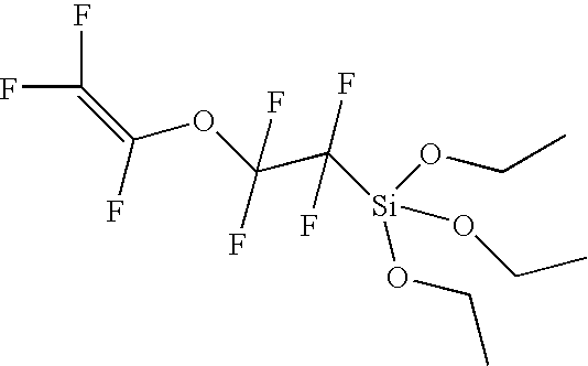
- Follow steps in Example 25, followed by
- 108.1 g (0.300 mol) tetrafluoroethyl trifluorovinyl ether triethoxysilane, 131 mL (1.800 mol, 214.1 g) thionylchloride and 4.51 g (0.039 mol) pyridinium hydrochloride are refluxed and stirred for 16 h. Excess of SOCl 2 is evaporated and tetrafluoroethyl trifluorovinyl ether trichlorosilane is isolated by vacuum-distillation.

- CF≡C—Li+ClSi(OEt)3→CF≡C—Si(OEt)3+LiCl
- 30.80 g (0.155 mol) ClSi(OEt) 3 in Et2O is slowly added to solution of CF≡C—Li (0.155 mol, 7.744 g, prepared in situ) in Et2O at −78° C. Reaction mixture is stirred overnight allowing it slowly warm to room temperature. LiCl is removed by filtration and solution evaporated to dryness to result fluoroacetylenetriethoxysilane.

- (C6F5)2Si(OEt)2+SOCl2→(C6F5)2Si(OEt)Cl+EtCl+SO2
- C6F5Li+(C6F5)2Si(OEt)Cl→(C6F5)3SiOEt+LiCl
- (C6F5)3SiOEt+SOCl2→(C6F5)3SiCl+EtCl+SO2
- 180.93 g (0.400 mol) di(pentafluorophenyl)diethoxysilane, 29 mL (0.400 mol, 47.6 g) thionylchloride and 4.92 g (0.0426 mol) pyridinium hydrochloride are refluxed and stirred for 16 h. Unreacted SOCl 2 is evaporated and di(pentafluorophenyl)chloroethoxysilane isolated by vacuum distillation.

- 88.54 g (0.200 mol) of di(pentafluorophenyl)chloroethoxysilane in Et 2O is slowly added to solution of C6F5-Li (0.200 mol, 34.80 g, prepared in situ) in Et2O at −78° C. The solution is stirred for over night allowing it to warm up to room temperature. Formed clear solution is filtered and evaporated to dryness to result tri(pentafluorophenyl)ethoxysilane, (C6F5)3SiOEt.

- Follow steps in Example 28, followed by
- 114.86 g (0.200 mol) tri(pentafluorophenyl)ethoxysilane, 14.6 mL (0.200 mol, 23.8 g) thionylchloride and 2.46 g (0.0213 mol) pyridinium hydrochloride are refluxed and stirred for 16 h. Unreacted SOCl 2 is evaporated and tri(pentafluorophenyl)chlorosilane isolated by vacuum-distillation.

- In addition to altering the organic groups in the above examples, it is of course also possible to use other reagents in the methods above. For example, in place of diethyl ether, other solvents such as THF could be used. In place of n-heptane (in Method A) other non polar solvents such as n-hexane could be used. And in place of thionyl chloride (for replacing one or more alkoxy groups with a halogen), chlorine, hydrochloric acid, hydrobromic acid, thionylbromide, chlorine or sulfurylchloride could be used. Also, the temperatures and times (and other process parameters) can be varied as desired. In one example, it is preferred that the molar ratio of the starting material to R 2X1 (Methods B or C) is 0.5:1 to 2:1—preferably 1:1. Also, the starting material and R2X1 are preferably mixed at a temperature less than 40C degrees, e.g. between −50C and −10° C. and warmed to a higher temperature over a period of four hours or more (this higher temperature can be room temperature or higher if desired)—or over a longer period of time such as overnight.
- As can be seen from the examples above, Methods B and C involve reacting a first compound (having an M group selected from
group 14 of the periodic table, 0, 1 or 2 organic groups bound to M) with a second compound (having an element from group 1 of the periodic table and a “new” organic group). As can also be seen from the above, such a reaction can take place if the first compound has alkoxy groups bound to M or both alkoxy and halogen groups (0, 1 or 2 halogen groups) bound to M. Method C, as mentioned earlier, is a variation of Method B—and both methods can be viewed as comprising: reacting a compound of the general formula R1 4-mMOR3 m-nXn, where R1 is any nonfluorinated (including deuterated) or partially or fully fluorinated organic group (preferably a partially or fully fluorinated aryl, alkenyl, alkynyl or alkyl group) as set forth above, where M is selected fromgroup 14 of the periodic table, where X is a halogen, where OR3 is an alkoxy group, where m=2 to 4 and n=0 to 2. R1 4-mMOR3 m-nXn is reacted with R2X1 where R2 is selected from alkyl, alkenyl, aryl or alkynyl (and where R2 is fluorinated (fully or partially), and where X1 is an element from group 1 of the periodic table. X1 is preferably Na, Li or K, more preferably Na or Li, and most preferably Li. M is preferably Si, Ge or Sn, more preferably Si or Ge, and most preferably Si. X is preferably Cl, Br or I, more preferably Cl or Br, and most preferably Cl. OR3 is preferably an alkoxy group having from 1 to 4 carbon atoms, more preferably from 1 to 3 carbons, and most preferably 2 carbons (ethoxy). Also, “m” is preferably 3 or 4, whereas “n” is preferably 0 or 1. - R 1 and R2 are independently preferably partially or fully fluorinated (though not necessarily as can be seen in prior examples) organic groups such as an aryl group (by aryl group we mean any organic group having a ring structure) though preferably a five or six carbon ring that is unsubstituted or substituted. For a six carbon ring structure, 1, 2 or 3 substituents can be bound to the ring, which substituents can be actively bound to the ring via a variation on the Method C set forth above (to be described further below). The substituents can be alkyl groups of any desired length, straight or branched chain, preferably fluorinated, and preferably having from 1 to 4 carbon atoms. Or the substituents on the ring structure can comprise a C═C double bond and be an alkenyl group (by alkenyl group we mean any organic group with a C═C double bond) such as an acrylate, vinyl or allyl group. A fluorinated vinyl, methyl or ethyl group on a fluorinated phenyl group are examples. Or, the aryl group could be a multi ring structure (e.g. perfluoronaphthalene or a biphenyl group). Or R1 and R2 could independently be an alkenyl group such as a vinyl or longer chain group having a C═C double bond, or a group having other types of double bonds (e.g C═O double bonds or both C═C and C═O double bonds) such as acrylate and methacrylate groups. R1 and R2 could also be an alkynyl group (by alkynyl group we mean any organic group with a carbon-carbon triple bond) as mentioned previously, as well as an alkyl group. If an alkyl group (by alkyl group we mean a carbon chain of any length), preferably the carbon chain is from 1 to 14, and more preferably from 4 to 8. Perfluorinated alkyl groups from 1 to 8 carbons can be used, as well as fluorinated (e.g. partially fluorinated) groups longer than 8 carbons. All the organic groups above could be deuterated in stead of fluorinated (or partially deuterated and partially fluorinated), though fully or partially fluorinated (particularly fully fluorinated) is preferred.
- In Method C set forth above, an organic (or hybrid) group “R” (e.g. R2) becomes bound to a group 3-6 or 13-16 element “M” by replacing a halogen “X” bound to “M” via the specified reaction. In an alternative to this method (Method D), an organic (or hybrid) group “R” (e.g. R1) comprises the halogen “X”—preferably Cl or Br (rather than “X” being bound to “M”). Thus when the reaction is performed, R2 replaces X bound to R1, such that R2 becomes bound to R1 (which is in turn bound to M). Preferably the other groups bound to M are alkoxy groups (OR3) or other organic groups. More particularly, such a method comprises providing a compound X aR1MOR3 2R4 where a is from 1 to 3, X is a halogen(s) bound to R1, R1 is an organic group (preferably an aryl, alkyl, alkenyl or alkynyl—more preferably an alkyl or aryl group), OR3 is an alkoxy, and R4 is either an additional alkoxy group or an additional organic group (selected from aryl, alkyl, alkenyl or alkynyl), and reacting this compound with R2M1 where M1 is selected from group 1 of the periodic table and R2 is an organic group preferably selected from aryl, alkyl, alkenyl and alkynyl, etc., so as to form R2 aR1MOR3 2R4.
- In one example, R 4 is an alkoxy group the same as OR3, such that the method comprises reacting XaR1MOR3 3 with R2M1 to form R2 aR1MOR3 3 (where R1 and OR3 are bound to M and R2 is bound to R1. In another example, R4 is an organic group selected from aryl, alkyl, alkenyl and alkynyl. Preferably OR3 is a methoxy, ethoxy or propoxy, R1 is an aryl or alkyl (straight or branched chain) having from 1 to 14 carbons, and R2 is an aryl, alkyl, alkenyl or alkynyl, where a=1 or 2 if R1 is an alkyl and a=1, 2 or 3 if R1 is an aryl group. R2 can be an epoxy, acrylate, methacrylate, vinyl, allyl or other group capable of cross linking when exposed to an electron beam or in the presence of a photoinitiator and electromagnetic energy (e.g. UV light).
- 1,4-Br2C6F4+Mg+Si(OEt)4→Br(C6F4)Si(OEt)3 1.
- Br(C6F4)Si(OEt)3+CF2═CFLi→(CF2═CF)(C6F4)Si(OEt)3 2.

- 250 g (0.812 mol) 1,4-dibromotetrafluorobenzene, 21.709 g (0.8932 mol) magnesium powder, small amount of iodine (15 crystals) and 181 mL (0.812 mol, 169.164 g) tetraethoxysilane were mixed together at room temperature and diethylether was added dropwise to the vigorously stirred solution until an exothermic reaction was observed (˜250 mL). After stirring at room temperature for 16 h diethylether was evaporated. An excess of n-heptane (˜600 mL) was added to precipitate the magnesium salts. Solution was filtrated and evaporated to dryness. The residue was fractionally distilled under reduced pressure to yield 4-bromotetrafluorophenyltriethoxysilane.

- 78.246 g (0.200 mol) 4-bromotetrafluorophenyltriethoxysilane in Et 2O is slowly added to solution of CF2═CF−Li (0.200 mol, 17.592 g, prepared in situ) in Et2O at −78° C. Reaction mixture is stirred overnight while it will slowly warm to room temperature. LiBr is removed by filtration and the product, 4-triethoxysilylperfluorostyrene, purified by distillation.

- 117.704 g (0.300 mol) 4-triethoxysilylperfluorostyrene, 131 mL (1.800 mol, 214.1 g) thionylchloride and 4.51 g (0.039 mol) pyridinium hydrochloride were refluxed and stirred for 16 h. Excess of SOCl 2 was evaporated and 4-trichlorosilyl-perfluorostyrene isolated by vacuum-distillation.

- The above example could be modified where 2 or 3 halogens (in this case Br) are bound to the phenyl group so as to result in multiple vinyl substituents. Also, the phenyl group could be another organic group such as an straight or branched chain alkyl group, a multi ring aryl group, etc., whereas the vinyl group could be any suitable organic group capable of binding to a group I element (in the above example Li) and replacing the halogen (in the above example Br). Examples other than vinyl include methyl, ethyl, propyl, phenyl, epoxy and acrylate.
- CF2C1-C(═O)—ONa+ClSi(OEt)3→CF2Cl—C(═O)—O−Si(OEt)3+NaCl
- CF2═CF—Li+CF2Cl—C(═O)—O—Si(OEt)3→CF2═CF—CF2—C(═O)—O—Si(OEt)3+LiCl
- 15.246 g (0.10 mol) sodium chlorodifluoroacetate, is dissolved to 100 mL Et 2O and cooled to −70° C. 19.7 mL (0.10 mol, 19.872 g) chlorotriethoxysilane in Et2O (50 mL) was added dropwise to reaction solution. The solution was stirred for over night allowing it to warm up to room temperature. NaCl is removed by filtration and solution evaporated to dryness to result clear colourless liquid, chlorodifluoroacetic acid, triethoxysilyl ester.

- 29.27 g (0.10 mol) chlorodifluoroacetic acid, triethoxysilyl ester, is dissolved to 100 mL Et 2O and slowly added to solution of CF2═CF—Li (0.10 mol, 8.796 g, prepared in situ) in Et2O at −78° C. Reaction mixture is stirred overnight allowing it slowly warm to room temperature. LiCl is removed by filtration and solution evaporated to dryness to result yellow liquid, crude perfluoro-3-butene acid, triethoxysilyl ester.

- Br(C6F4)Si(OEt)3+C6F5—Li→C6F5—C6F4—Si(OEt)3+LiBr

- 78.246 g (0.200 mol) 4-bromotetrafluorophenyltriethoxysilane in Et 2O is slowly added to solution of C6F5-Li (0.200 mol, 34.80 g, prepared in situ) in Et2O at −78° C. Reaction mixture is stirred overnight while it will slowly

- warm to room temperature. LiBr is removed by filtration and the product, perfluorobiphenyltriethoxysilane, purified by distillation.
- 143.516 g (0.300 mol) perfluorobiphenyltriethoxysilane, 131 mL (1.800 mol, 214.1 g) thionylchloride and 4.51 g (0.039 mol) pyridinium hydrochloride were refluxed and stirred for 16 h. Excess of SOCl 2 was evaporated and perfluorobiphenyltrichlorosilane isolated by vacuum-distillation.

- 1,4-Br2C4F8+Mg+Si(OEt)4→Br(CF2)4Si(OEt)3
- Br(CF2)4Si(OEt)3+CF2═CFLi→CF2═CF—(CF2)4—Si(OEt)3

- 143.94 g (0.40 mol) 1,4-dibromooctafluorobutane, 10.69 g (0.44 mol) magnesium powder, small amount of iodine (15 crystals) and 88 mL (0.40 mol, 82.42 g) tetraethoxysilane were mixed together at room temperature and diethylether was added dropwise to the vigorously stirred solution until an exothermic reaction was observed (˜200 mL). After stirring at room temperature for 16 h diethylether was evaporated. An excess of n-heptane (˜400 mL) was added to precipitate the magnesium salts. Solution was filtrated and evaporated to dryness. The residue was fractionally distilled under reduced pressure to yield 4-bromooctafluorobutanetriethoxysilane.

- 88.641 g (0.200 mol) 4-bromooctafluorobutanetriethoxysilane in Et 2O is slowly added to solution of CF2═CF—Li (0.200 mol, 17.592 g, prepared in situ) in Et2O at −78° C. Reaction mixture is stirred overnight while it will slowly warm to room temperature. LiBr is removed by filtration and the product, perfluoro-1-hexenetriethoxysilane, purified by distillation.

- 133.295 g (0.300 mol) perfluoro-1-hexenetriethoxysilane, 131 mL (1.800 mol, 214.1 g) thionylchloride and 4.51 g (0.039 mol) pyridinium hydrochloride were refluxed and stirred for 16 h. Excess of SOCl 2 was evaporated and perfluoro-1-hexenetrichlorosilane isolated by vacuum-distillation.

- In the above “Method D” examples, R 1, R2, R3 and R4 are preferably partially or fully fluorinated.
- Hydrolysis and Condensation of the Compound(s):
- Compounds IV, VII and IX have organic (or hybrid) R group(s) and halogen(s) (preferably Br or Cl) bound to M (selected from groups 3-6 or 13-16—preferably group 14)). These compounds can be hydrolyzed alone or in any combination to result in a material having a -M-O-M-O— backbone with R groups bound to the backbone, and that preferably has a molecular weight of from 500 to 10,000 (more preferably from 500 to 5000). In one example, a compound selected from Compound IV is hydrolyzed with another compound selected from Compound IV. In another example, a single compound from Compound VII is hydrolyzed. Many other combinations are possible, including: a) Compound IV+Compound VII; b) Compound IV+Compound IV+Compound IV; c) Compound VII+Compound VII; d) Compound IV+Compound VII+Compound IX; e) Compound IV+Compound IV+Compound IX; f) Compound VII+Compound IX, etc. Any other combinations, in any desired ratio, can be used for the hydrolysis and eventual deposition.
- The hydrolysis/condensation procedure can comprise five sequential stages: Dissolvement, hydrolysis and co-condensation, neutralization, condensation and stabilization. Not all stages are necessary in all cases. In the hydrolysis, chlorine atoms are replaced with hydroxyl groups in the silane molecule. The following description takes as an example compounds that have chlorine as the halogen that takes part in the hydrolysis reaction, and silicon is the metal in the compound. Hydrochloric acid formed in the hydrolysis is removed in the neutralization stage. Silanols formed in the hydrolysis are attached together for a suitable oligomer in the condensation stage. The oligomer formed in the condensation are stabilized in the end. Each stage can be done with several different ways.
- Dissolvement. Chlorosilanes are mixed together in an appropriate reaction container and the mixture is dissolved into a suitable solvent like tetrahydrofuran. Instead of tetrahydrofuran, other solvents can be used (pure or as a mixture): acetone, chloroform, diethyl ether, ethyl acetate, methyl-isobutyl ketone, methyl ethyl ketone, acetonitrile, ethylene glycol dimethyl ether, triethylamine, formic acid, nitromethane, 1,4-dioxan, pyridine, acetic acid.
- Hydrolysis. The reaction mixture is cooled to 0° C. The hydrolysis is performed by adding water (H 2O) into the reaction mixture. The water is added in 1:4 (volume/volume) water-tetrahydrofuran-solution. Water is used equimolar amount as there are chlorine atoms in the starting reagents. The reaction mixture is held at 0° C. temperature during the addition. The reaction mixture is stirred at room temperature for 1 hour after addition. Instead of tetrahydrofuran, water can be dissolved into pure or mixture of following solvents: acetone, chloroform, diethyl ether, ethyl acetate, methyl-isobutyl ketone, methyl ethyl ketone, acetonitrile, ethylene glycol dimethyl ether, triethylamine, formic acid, nitromethane, 1,4-dioxan, pyridine, acetic acid. In the place of water (H2O) can be used: deuterium oxide (D2O) or HDO. A part of the water can be replaced with alcohols, deuterium alcohols, fluorinated alcohols, chlorinated alcohols, fluorinated deuterated alcohols, and/or chlorinated deuterated alcohols. The reaction mixture may be adjusted to any appropriate temperature. Excess of water can be used. Some level co-condensation can happen during the hydrolysis that can be seen as increment of material molecular mass.
- Neutralization. The reaction mixture is neutralized with pure sodium hydrogen carbonate. NaHCO 3 is added into cooled reaction mixture at 0° C. temperature (NaHCO3 is added equimolar amount as there is hydrochloric acid in the reaction mixture). The mixture is stirred at the room temperature for a while. After the pH of the reaction mixture has reached value 7, the mixture is filtered. The solvent is then evaporated with rotary evaporator (p=250−50 mbar, t(bath)=+30° C.).
- Instead of NaHCO 3 can be used pure potassium hydrogen carbonate (KHCO3), sodium carbonate (Na2CO3), potassium carbonate (K2CO3), sodium hydroxide (NaOH), potassium hydroxide (KOH), calcium hydroxide (Ca(OH)2), magnesium hydroxide (Mg(OH)2) ammonia (NH3), trialkylamines (R3N, where R is hydrogen or straight/branched chain CxHy, x<10, for example triethanolamine), trialkyl ammonium hydroxides (R3NOH, R3N, where R is hydrogen or straight/branched chain CxHy, x<10). All neutralization reagents can be added into the reaction mixture also as a solution of any appropriate solvent. Neutralization can be performed also with solvent-solvent—extraction or with azeotropic water evaporation.
- Procedure for solvent-solvent-extraction: The solvent is evaporated off after the hydrolysis. The material is dissolved into pure or mixture of solvents such as: chloroform, ethyl acetate, diethyl ether, di-isopropyl ether, dichloromethane, methyl-isobutyl ketone, toluene, carbon disulphide, carbon tetrachloride, benzene, nitromethane, mehylcyclohexane, or chlorobenzene. The solution is extracted several times with water or D 2O until the pH of the organic layer is over value 6. The solvent is then evaporated with rotary evaporator (p=250−50 mbar, t(bath)=+30° C.).
- Procedure for azeotropic water evaporation: The solvent is evaporated off after the hydrolysis. The material is dissolved into mixture of water and one of the following solvents (1:10 volume/volume): tetrahydrofuran, ethanol, acetonitrile, 2-propanol, tert-butanol, ethylene glycol dimethyl ether, triethylamine, 2-propanol. The formed solution is evaporated to dryness. The material is dissolved again into the same mixture of water and the solvent. Evaporation and addition cycle is repeated until pH value of the material solution is 7. The solvent is then evaporated with rotary evaporator (p=250−50 mbar, t(bath)=+30° C.).
- Neutralization stage in cases where condensation stage is passed: In the neutralization stage evaporation of the solvent in the end is not necessary always. In these cases this stage is aborted after filtering (the reaction mixture is neutral) and the synthesis is continued in stabilization stage (the condensation stage is passed).
- Condensation. The material is stirred with magnetic stirrer bar under 12 mbar pressure for few hours. Water, which forms during this final condensation, evaporates off. The pressure in this stage can be in a large range. The material can be heated while vacuum treatment. In some cases this stage is not necessary.
- Stabilization. The material is dissolved into cyclohexanone, which is added 30 weight-% of the materials weight. The pH of the solution is adjusted to value 2,0 with acetic acid. In the place of cyclohexanone can be used any of a number of other solvents, (alone or as a mixture), such as methyl-isobutyl ketone, 2-propanol, ethanol, methanol, 1-propanol, tetrahydrofuran, acetone, nitromethane, chlorobenzene, dibutyl ether, mesitylene, 1,1,2,2-tetrachloroethane, trichloroethanes, ethyl lactate, 1,2-propanediol monomethyl ether acetate and/or carbon tetrachloride. In the place of acetic acid can be used regular or deuterated forms of following acids, among others: formic acid, propanoic acid, monofluoro acetic acid, trifluoro acetic acid, trichloro acetic acid, dichloro acetic acid and/or monobromo acetic acid.
- Stabilization in cases when the condensation stage is bypassed: Acetic acid is added into the mixture until a pH value of 3-4 is reached. The solution is evaporated until appropriate concentration of the oligomer in the solution has reached (about 50 w-% oligomer, 49 w-% solvent and 1 w-% acid, “solvent” is the solvent of the dissolvement and hydrolysis stages).
- In Example I above, “chlorosilanes” are initially mixed together with tetrahydrofuran. As mentioned earlier, this can be an almost unlimited number and type of compounds as disclosed in detail earlier herein—including a large number of chlorosilanes and other halo-metal-organic compounds in accordance with the invention and in accordance with the ultimate properties desired in the final material. If one of the compounds to be hydrolyzed and condensed is pentafluorophenyltrichlorosilane, this can be prepared as in the methods set forth above, by:
- C6F5Br+Mg+excess Si(OEt)4→C6F5Si(OEt)3+(C6F5)2Si(OEt)2
- C6F5Si(OEt)3+SOCl2+py.HCl→C6F5SiCl3
- 100 mL (0.8021 mol, 198.088 g) pentafluorobromobenzene, 24.90 g (1.024 mol) magnesium powder and 716 mL (3.2084 mol, 668.403 g) tetraethoxysilane are mixed together at room temperature and diethylether is added dropwise to the vigorously stirred solution until an exothermic reaction is observed (˜200 mL). After stirring at 35° C. for 16 h the mixture is cooled to room temperature and diethylether evaporated. An excess of n-heptane (˜500 mL) is added to precipitate the magnesium salts. Solution is filtrated and evaporated to dryness. The residue is fractionally distilled under reduced pressure to yield pentafluorophenyltriethoxysilane.

- 100 mL (0.375 mol, 124.0 g) pentafluorophenyltriethoxysilane, 167 mL (2.29 mol, 272.0 g) thionylchloride and 5.63 g (0.0487 mol) pyridinium hydrochloride are refluxed and stirred for 24 h. Excess of SOCl 2 is evaporated and pentafluorophenyltrichlorosilane

- isolated by vacuum-distillation.
- If a second of the compounds to be hydrolyzed and condensed is trifluorovinyltrichlorosilane, this can be prepared by:
- 119 mL (0.155 mol) sec-butyllithium (1.3 M solution in cyclohexane) is added under argon with stirring to 18.053 g (0.155 mol) chlorotrifluoroethylene

- dissolved in Et 2O at −80° C. After the addition is complete the reaction mixture is stirred for 15 min to yield lithiumtrifluoroethylene.

- 30.80 g (0.155 mol) ClSi(OEt) 3 in Et2O is slowly added to solution of CF2═CF—Li (0.155 mol, 13.633 g, prepared in situ) in Et2O at −78° C. Reaction mixture is stirred overnight while it will slowly warm to room temperature. LiCl is removed by filtration and the product, trifluorovinyltriethoxysilane,

- is isolated by distillation.
- 24.4 g (0.100 mol) trifluorovinyltriethoxysilane, 44 mL (0.60 mol, 71.4 g) thionylchloride and 0.497 g (0.0045 mol) pyridinium hydrochloride are refluxed and stirred for 24 h. Excess of SOCl 2 is evaporated and trifluorovinyltrichlorosilane

- is purified by distillation.
- Then, to a solution of trifluorovinyltrichlorosilane and pentafluorophenyltrichlorosilane at a molar ratio 1:1 in dehydrated tetrahydrofuran, is added dropwise a stoichiometric amount of water (e.g. H2O or D2O) in THF at 0° C. (nonstoichiometric amounts, higher or lower, can also be used). After stirring for 1 hour, the solution is neutralized with 3 equivalents of sodium hydrogencarbonate. After confirming the completion of generation of carbonic acid gas from the reaction solution, the solution is filtered and volatile compounds are removed by vacuum evaporation to obtain colorless, transparent viscous liquid, poly(pentafluorophenyltrifluorovinyl-siloxane), in a three dimensional network of alternating silicon and oxygen atoms.

- The above is but one example of a method comprising: reacting a compound of the general formula R1MX3 3 with a compound of the general formula R2MX33 where R1 is selected from alkyl, alkenyl, aryl and alkynyl, R2 is selected from alkenyl, aryl or alkynyl, M is an element selected from groups 3-6 or 13-16 though preferably from
group 14 of the periodic table, and X3 is a halogen; with H2O or D2O; so as to form a compound having a molecular weight of from 500 to 10,000 with a -M-O-M-O— backbone with R1 and R2 substituents on each M. In the hydrolysis example above, silicon atoms of the network are modified by pentafluorophenyl and trifluorovinyl groups in an approximate ratio 1:1. Of course other ratios are possible depending upon the ratio of starting materials, and, of course, other three dimensional networks can be achieved by having other (or additional) starting materials selected from Compound IV, VII and IX, along with other hydrolyzable materials. An alternate example is a method comprising: reacting a compound of the general formula R1R2MX32 where R1 is selected from alkyl, alkenyl, aryl and alkynyl, R2 is selected from alkenyl, aryl or alkynyl, M is an element selected fromgroup 14 of the periodic table, and X3 is a halogen; with D2O; so as to form a compound having a molecular weight of from 500 to 10,000 with a -M-O-M-O— backbone with R1 and R2 substituents on each M. As mentioned above, Compounds IV, VII and IX have organic (or hybrid) R group(s) and halogen(s) (preferably Br or Cl) bound to M (selected from groups 3-6 or 13-16—preferably group 14)) and can be combined in almost limitless combinations—e.g. a compound selected from the Compound IV group could be hydrolyzed with another compound selected from Compound IV. In another example, a single compound from Compound VII is hydrolyzed. Many other combinations are possible, including: Compound IV+Compound VII; Compound IV+Compound IV+Compound IV; Compound VII+Compound VII; Compound IV+Compound VII+Compound IX; Compound IV+Compound IV+Compound IX; Compound VII+Compound IX, etc.—which various combinations of compounds will result in a hydrolyzed material having at least one organic substituent bound to an inorganic oxide backbone—preferably from 2 to 6 different organic substituents bound to the backbone prior to deposition and exposure. The presence of the organic groups, preferably all fluorinated, allows for improved optical absorption characteristics due to minimal or absent C—H bonds in the deposited material (preferably the hydrolyzed/condensed material has a hydrogen content of 10% or less, preferably 5% or less, and more preferably 1% or less). - Also, though “M” in the above hydrolysis example is silicon, it is possible to have materials with other M groups, or “dope” one or more silanes to be hydrolyzed with a lesser (though not necessarily lesser) amount of a compound having a different M group such as boron, a metalloid and/or an early transition metal (e.g. B, Al, Si, Ge, Sn, Sb, Pb, Ta, Ti, Zr, Er, Yb and/or Nb). As an example, a material could be formed from hydrolyzing/condensing one or more compounds each formed of silicon, chlorine and one or more fluorinated organic compounds bound to the silicon, whereas another material could be formed by hydrolyzing/condensing such compound with one or more additional compounds that each comprise an element other than silicon (Ge, Nb, Yb etc.), chlorine and one or more fluorinated organic groups. In this way, the inorganic backbone of the hydrolyzed/condensed material will comprise silicon, oxygen and the element(s) other than silicon, with fluorinated organic groups bound to this backbone. This “modified backbone” can result in a material refractive index different than one having an inorganic backbone comprising silicon and oxygen alone. Such an ability to modify the refractive index is desirable for forming core and cladding layers in a waveguide.
- Deposition of the Hydrolyzed and Condensed Material:
- The material formed as above preferably has a molecular weight between 500 and 10,000, more preferably between 500 and 5000. Other molecular weights are possible within the scope of the invention, however a weight between 500 and 5000 provides the best properties for depositing the material on a substrate. The substrate can be any suitable substrate, such as any article of manufacture that could benefit from a hydrophobic and/or transparent layer or coating. In the fields of electronics and optical communications, the material could be deposited as a final passivation layer, as a glob top coating, as an underfill in a flip chip process, as a hermetic packaging layer, etc. Because the material can be patterned as will be discussed further below, the material could be deposited on a substrate (e.g. a glass, quartz, silicon or other wafer) as a buffer/cladding, waveguide/core or other layer within a waveguide or other optoelectronic/photonic device. In general, the siloxane oligomer—the hybrid organic-inorganic material having the molecular weight as set forth above—is mixed with a suitable solvent and deposited. The solvent can be any suitable solvent, such as isopropanol, ethanol, methanol, THF, mesitylene, toluene, cyclohexanone, cyclopentanone, dioxane, methyl isobutyl ketone, or perfluorinated toluene.
- Deposition is generally at a temperature of 200C or less (can be at 150C or less). If the material is annealed after deposition, it is preferably at 200C or less. If the material is to be patterned by exposure to electromagnetic radiation (e.g. UV light) then a photoinitiator can be mixed into the material along with the solvent. There are many suitable types of photoinitiators that could be used, such as Irgacure 184, Irgacure 500, Irgacure 784, Irgacure 819, Irgacure 1300, Irgacure 1800, Darocure 1173 or Darocure 4265. The initiator could be highly fluorinated, such as 1,4-bis(pentafluorobenzoyl)benzene or Rhodosil 2074 photoinitiator. Also, thermal initiators can be applied for thermal crosslinking of organic carbon double bond moieties, such as with Benzoyl peroxide, 2,2′—Azobisisobutyronitrile, or tert-Butyl hydroperoxide. The amount of these photo or thermal initiators may vary from 0.1 to 5 w-%. They may appear in solid or liquid phase. The initiator is carefully mixed with the material that already contains “processing solvent”. (Organic dopants or liquid crystal dopants—or erbium—can be mixed with the material at this point if desired.) Finally the material is filtered through inert semiconductor grade filter to remove all undissolved material.
- Spin-on processing. After hydrolysis and condensation, the material solution is deposited on a substrate in a spin-on process (or by dipping, spray and meniscus coating, etc.). Both static and dynamic deposition can be used. The material is first spread over a wafer or other substrate at low speed (50 to 700 rpm) for 5 to 10 seconds and then the speed is increased by 500 to 5000 rpm/s acceleration to 1000 rpm or higher depending upon starting speed. However, slower speeds may be used if very thick films are required. If 1000 rpm spinning speed is applied film thicknesses from 100 nm to 30,000 nm are achieved depending on material viscosity. Material viscosity can be tuned by increasing the amount of process solvent, which typically have relative low vapor pressure and high boiling point. Spinning is continued for 30 to 60 seconds to obtain uniform film over the wafer. After the spinning, an edge bead removal process is accomplished and the wafer is pre-baked (in nitrogen on hot-plate or in furnace) at temperature around 100 Celsius for 1 minute to remove the process solvent (if used) and improve adhesion to the substrate or to the layer underneath of the current material. Similar spin cycles are applicable for all three main optical layers, which are buffer, core and cladding layers. Adhesion promoter such as 1% aminopropyltrimethoxy silane in IPA or plasma activation may be applied between the main optical layers to improve adhesion between them.
- The substrate can be any suitable substrate or article. In many cases, the substrate will be a planar wafer-type substrate, such as a glass, plastic, quartz, sapphire, ceramic or a semiconductor substrate (e.g. germanium or silicon). The substrate can have electronic or photonic circuitry thereon. For example, the substrate could be an integrated circuit or a printed circuit board. Or, a light emittor or photodetector could be provided on the substrate prior to deposition of the hydrophobic hybrid material of the invention (or such an additional optical component could be “dropped in” after deposition of the material. The photodetector could be an avalanche photodiode or PIN diode, whereas the light emittor could be a laser (e.g. VCSEL) or LED (e.g. OLED). Or, the light emittor could be a monolithic Fabry-Perot laser, a monolithic Bragg laser, a monolithic distributed feedback laser or a semconductor quantum well laser. The light emittor could also be a single frequency laser (e.g. a distributed feedback laser) or a multi-frequency laser (e.g. an integrated cavity laser or an arrayed laser).
- There is essentially no limit to the number or types of photonic or electronic devices that could be integrated with the deposited material—whether the material is used as a simple coating or passivation layer, or as a waveguide (of course, if the material forms the cladding and/or core layers of a waveguide, it is preferable that the other optical component(s) is disposed so as to properly direct or receive light into or out of the waveguide (in a simple example, the waveguide acts as a coupler between a fiber and the photodetector or light emittor). Other optical devices that could be formed on the substrate, or in communication with the waveguide, include N-port splitters with cascading Y couplers, planar crossovers, amplifiers, switches, wavelength division multiplexor receiver assemblies, arrayed waveguide gratings, PIN diode receivers, external modulators, combiners, amplifiers (e.g. multistage EDFA), isolators, resonant couplers, wavelength couplers or splitters, waveguide grating routers, filters, integrated EDWAs, monolithic DCMs, reonfigurable OADMs, optical channel monitors, thermo optic VOAs, dispersion compensators, gain flatterners, tunable waveguide gratings, waveguide polarizers, splitters, interleavers, taps, etc. Or, the material of the invention could be used to form the optical device components themselves, if desired.
- Add 10 w-% of methyl isobutyl ketone and 1 w-% of Darocure 1173 photoinitiator to result in the formation of a spin-coatable and photo-sensitive material. The material is deposited by spin coating, spray coating, dip coating, etc. onto a substrate or other article of manufacture. As mentioned herein, many other organic groups can be used in place of the above groups, though preferably one of the groups in one of the compounds is capable of cross linking when exposed to electromagnetic energy (or an electron beam)—e.g. an organic group with a ring structure (e.g. an epoxy) or a double bond (e.g. vinyl, allyl, acrylate, etc.). And, preferably such a cross linking group is partially or fully fluorinated so that the organic cross linking groups in the material after cross linking will be fluorinated cross linking groups—ideally perfluorocarbon cross linking groups in the finally formed material.
- Exposure:
- One use of the material set forth above is as a layer within a waveguide. However, as mentioned elsewhere herein, many other devices, from simple hydrophobic coatings to complex optical devices, can be formed from the materials and methods described above. Regardless of the article being formed, it will be desirable to cross link the deposited material. As mentioned above, any suitable cross linking agent can be used, including common thermal and photo initiators. Assuming that a photoinitiator has been used, then the deposited core layer material acts as a negative tone photoresist, i.e. exposed regions becomes less soluble in a developer. The deposited material can be exposed with any suitable electromagnetic energy, though preferably having a wavelength from 13 nm to 700 nm, including DUV (210-280 nm), mid-UV (280-310 nm), standard I-line or G-line UV-light. DUV exposure is preferred. A stepper can be used for the UV exposure. Typically contact mask exposure techniques are applied. Exposure times may vary between 1 second to several hundred seconds. After the exposure the unexposed areas are removed by soaking the substrate/article (e.g. wafer) or otherwise exposing the substrate/article to a suitable developer (e.g. spray-development may also be used). A developer such as Dow Chemical DS2100, Isopropanol, methyl isobutyl ketone etc. or their combinations can be used to remove unexposed material. Typically 2 minutes development time is used and a solvent rinse (e.g. an ethanol rinse) is preferred to finalize the development. The rinsing removes development residues from the wafer. The adhesion of the exposed structures and the effectiveness of the exposure can be increased by heat-treating the article/substrate (e.g. a slow anneal at elevated temperature—typically less than 200 C). Other exposure techniques, such as exposure with a laser or with Deep UV, could also be performed in place of the above.
- Post-baking process. The final hardening of the material is achieved by baking (in air, nitrogen, argon or helium) the article/substrate for several hours typically at less than 200 C. Step-wise heating ramp-up and ramp-down are preferred. The material can also be fully or partially hardened with deep UV light curing.
- In the alternative to the above, the material to be patterned is spun on, prebaked, hard baked (typically less than 200 C). Then standard photoresist and RIE etching techniques are applied.
- Waveguide:
- If the article being formed is a waveguide, the substrate could be a PCB, IC, silicon, glass or quartz wafer, etc., upon which is deposited a lower cladding layer. (A buffer layer can first be deposited if desired.) The cladding layer is made by forming Compounds IV, VII and/or IX and hydrolyzing such compound(s), followed by mixing the hydrolyzed material with a solvent and thermal initiator and then depositing onto the substrate, as set forth in further detail above. After deposition, the cladding layer can be exposed to UV light and/or baked to solidify the cladding. On the cladding layer is deposited a core layer that is made and deposited as above, except with a different ratio of compounds or different compounds that are hydrolyzed/condensed to form the material ready for deposition. By modifying the hydrolysable compounds and/or ratios of compounds in the core layer vs. those in the cladding layer, a different index of refraction is achieved. A developer (e.g. e.g. methanol, ethanol, propanol, acetone, methyl isobutyl ketone, tetrahydrofuran, Dow Chemical DS2100, Dow Chemical DS3000, etc.) is then applied to remove unexposed material. In this way, a core for the waveguide is formed. Then an upper cladding layer is made and deposited in the same way as the lower cladding layer. Though in this example the mask is a binary mask (the material is either fully exposed or not exposed to electromagnetic radiation), it is also possible to provide partial exposure (e.g. in a continuum from full exposure to a low or non-exposure level as in a gray scale mask). Such a gray scale exposure can form a vertical taper in the waveguide when the developer is applied.
- More particularly, as can be seen in FIG. 3A, a
substrate 10 is provided, on which is deposited a lower cladding layer 12 (FIG. 3B). A buffer layer could be deposited prior to depositing the lower cladding layer, depending in part on the thickness of the lower cladding layer that is deposited. After depositing the lower cladding layer, acore layer 14 is deposited (FIG. 3C).Core layer 14 preferably has a different refractive index than the lower cladding layer.Core layer 14 is then patterned, preferably by exposure to light (preferably UV light) via a mask 20 (FIG. 3D). Areas that are exposed to light undergo cross linking and hardening. As can be seen in FIG. 3E, application of a developer allows for removal of unexposed areas, with exposedareas 141 of the core layer remaining (now the core). Baking/annealing can be used to stabilize the remaining areas of the core layer. As can be seen in FIG. 3F, anupper cladding layer 16 is deposited, followed by a final hard bake. Preferablyupper cladding layer 16 has a different refractive index thancore 141, which refractive index can be the same as that of thelower cladding layer 12. A cross section photograph of a patterned core, in accordance with the method of FIGS. 3A to 3F, is illustrated in FIG. 5. - An alternate process for forming a waveguide is illustrated in FIG. 4A, a
substrate 30 is provided, upon which is deposited a lower cladding layer 32 (FIG. 4B). As above, a buffer layer could also be provided, prior to depositing the lower cladding layer, if desired. The substrate and any layers thereon can be heated to stabilize the deposited layer(s). As can be seen in FIG. 4C, acore layer 34 is provided preferably having a refractive index different than the refractive index of the lower cladding layer. Then, as can be seen in FIG. 4D, a photoresist layer 36 (e.g. positive tone) is deposited (preferably by spin-on), followed by a pre-bake. Then, the photoresist is exposed to electromagnetic radiation in FIG. 4E (e.g. UV light—wavelength depending upon the type of photoresist selected), and exposed to a developer (FIG. 4F) to remove exposed areas of resist, leaving behind unexposed resistareas 36 1. Then,core layer 34 is etched, such as by reactive ion etching, so as to remove areas of core layer not protected by resistareas 36 1—leaving behindcore layer portion 34 1. Finally, resistportions 36 1 are removed, and, as illustrated in FIG. 4H, anupper cladding layer 38 is deposited, followed by heating of the thus formed waveguide. Any of the cladding layers and core layer (as well as buffer layer if included) can be formed of the hydrophobic material of the invention. Of course, the cladding layers preferably have a different refractive index than the core, which refractive index can be achieved by modifying the inorganic backbone and/or the organic groups bound thereto, as mentioned elsewhere herein. - Material Characteristics:
- Material processed and formed on a substrate as above, was tested to determine various characteristics of the deposited and cross linked material. In a test of the hydrophobicity of the material, a water contact angle measurement can be measured. The phenomenon of wetting or non-wetting of a solid by a liquid can be understood in terms of the contact angle. A drop of a liquid resting on a solid surface forming an angle relative to the surface may be considered as resting in equilibrium by balancing the three forces involved (namely, the interfacial tensions between solid and liquid, that between solid and vapor and that between liquid and vapor). The angle within the liquid phase is known the contact angle or wetting angle. It is the angle included between the tangent plane to the surface of the liquid and the tangent plane to the surface of the solid, at any point along their line of contact. The surface tension of the solid will favor spreading of the liquid, but this is opposed by the solid-liquid interfacial tension and the vector of the surface tension of the liquid in the plane of the solid surface. This angle can be better seen in FIG. 1, where the alpha angle is subtracted from 180 degrees, to result in the contact angle. A photograph of a water droplet on a hydrophobic surface is shown in FIG. 2.
- In the present invention, contact angles of 90 degrees or more, and generally 100 degrees or more are easily achieved (from 50 ul of ultrapure water). Depending upon the compounds selected for hydrolysis/condensation, water contact angles of 125 degrees or more, or even 150 degrees or more can be achieved. Particularly if all organic groups, including those that provide bulk to the final material (e.g. a longer alkyl chain or a single or multi ring aryl group) as well as those that allow for cross linking (e.g. organic groups with unsaturated double bonds), are fully fluorinated—then the resulting material can be highly hydrophobic and result in very large contact angles. The hydrophobicity can easily be tailored depending upon which compounds are selected, and in what amounts, for hydrolysis/condensation.
- The optical loss of the materials were also tested and determined to be less than 0.1 dB/cm at 1550 nm. The optical loss can be less than 0.09 dB/cm (or even less than 0.075 dB/cm or less than 0.05 dB/cm) at 1550 nm, depending upon which compounds and in what amounts are selected for hydrolysis/condensation, and in particular the level of fluorination of the compounds selected. The deposited materials tested also have an optical loss less than 0.1 dB/cm (or even less than 0.075 dB/cm) at 1310 nm, C Band and L Band. The optical bulk loss measurement was carried out from bulk sample of the optical material by using Varian Gary 5 UV-Vis-IR spectrophotometer.
- Polarization Dependent Loss (PDL) measurements were made on a formed waveguide. Equipment used for PDL measurements, included a red light source, a laser source, a coupler, a polarization controller, input and output single mode fibres, a detector, alignment stages, a fibre coupler, a lens and a screen: Align input fibre directly to output fibre, moving fibre holders nearer each other as required. Ensure the red light source is switched off and the polarization controller is not scanning. Dispense a bead of index matching fluid between fibres and optimize the alignment using the laser and power meter. Ensure the averaging time of the detector is 20 ms and the wavelength is 1550 nm. Set the polarization controller scanning on scan speed 5. Wait for 10 s and record the maximum and minimum power levels. Stop the polarization controller scanning. Plot the average and the PDL on the chart. Make sure values are within acceptable limits. Then, turn red light source on and laser off. Wipe the facets of the chip gently with IPA and place it on the holder. Looking through the microscope, roughly align the input fibre to the desired waveguide. Place the lens on the output stage, about 7 mm from the output facet. Align the input fibre vertically until a red line is observed on the screen. Focus the line on the screen by moving the lens nearer or further from the chip. Scan the input fibre across the input of the chip until a spot is observed on the screen. Check using the microscope that the fibre is aligned to the correct waveguide still. Then, remove the lens and replace with the output fibre. Using the microscope, position the fibre near the desired waveguide, about 100 um (the width of the fibre) back from the chip. Turn the red light off and the laser on. Move the output fibre vertically until the power is maximized. Move the output fibre horizontally until the power is maximized. Dispense a bead of index fluid on the input and output facets. Finely adjust all axes until the power is optimized. Then, scan the polarization controller and wait for 10 seconds. Record the maximum and minimum power levels, calculating the average loss and the PDL. To measure the next waveguide, retract the input and output fibres slightly and index the center stage to the next waveguide. The power meter will indicate when the next waveguide is in position. Return to the ‘chip alignment’ stage. Polarization dependent loss was found to be 0.1 dB/cm or less, and generally 0.05 dB/cm or less. In some cases, the PDL was 0.01 dB/cm or less. Birefringence measurements were also performed on the materials.
- Birefringence was found to be less than 5×e-5, and in many cases less than 2×10e-5 (or as low as 1×10e-6) depending upon the compounds selected for hydrolysis/condensation. The birefringence of the slab optical films were measured on a SCI FilmTech 4000. Stability of deposited materials of the invention was determined by the so-called “pressure cooking” testing procedure. In this procedure, the material was deposited on a substrate and, after cross linking (thermal and/or light exposed cross linking depending upon the initiator used), tested for optical properties such as optical absorbance, polarization dependent loss and refractive index. Then, the material was placed into a pressure chamber that contains an amount of water. The chamber was heated up to 120 C and maintained at a pressure of 2 atm, at which point the water formed supercritical water vapor. The material was held in this environment for 2 hours and then removed and tested optically (optical absorbance, polarization dependent loss and refractive index). It was found that the material was still present on the substrate and had not been changed structurally. Also, the optical testing showed that optical absorbance, polarization dependent loss and index of refraction each remained within 5% (in most cases within 1%) of the original values prior to the exposure to the supercritical water. The testing showed a high level of stability not normally found in optical materials having an organic component such as the materials of the present invention.
- Other properties of the materials, such as surface and sidewall roughness, feature size, aspect ratio, and glass transition temperature were also measured. The glass transition temperature, Tg, of the deposited materials was measured using a Mettler-Toledo Differential Scanning Calorimeter (DSC) and found to be 200 C or greater, and generally 250 C or greater (or even 310 C or more). Surface roughness, Rq, of the material (measured by atomic force microscopy and WYKO—white light interferometry) was found to be 10 nm or less, and generally 5 nm or less. In many cases, the surface roughness is 1 nm or less. When the material is patterned, sidewalls are formed in the surface topography that is created. A measurement of the sidewall roughness (measured by atomic force microscopy, SEM and WYKO—white light interferometry) was found to be 50 nm or less, and generally 10 nm or less. Depending upon the compounds used for hydrolysis/condensation, as well as exposure and development technique, a sidewall roughness, Rq, or 5 nm or less, or even 1 nm or less, can be achieved. Patterning of the material was able to create feature sizes (e.g. ridge or trench width) as small as 100 nm or less, or even 50 nm or less, as well as aspect ratios of such features of 2:1, 3:1 or even as high as 10:1 (also measured by atomic force microscopy, SEM and WYKO—white light interferometry).
- Due to the hydrophobic nature of the layer(s) deposited in the present invention, it may be desirable in some cases to first provide an adhesion promoting layer before depositing the hydrophobic material. For example, a 1:100 dilution of SOD could be applied as an adhesion promoting layer before spinning on (or otherwise depositing) the hybrid hydrophobic material. The diluted SOD is very stable (photo, thermal, humidity, 85/85 tests) and easy to detect, spreads well on Silicon and is optically clear all the way to UV
- Other adhesion promoting materials that could be used include Onichem organosilane G602, (N (beta aminoethyl)-gamma aminopropyl dimethyl siloxane (CA 3069-29-2)—high boiling, high R 1(1.454), thermally stable low density and is compatible with acrylics, silicones, epoxies, and phenolics), or Dow AP8000, propyloxysilane (e.g. 3(2 3 epoxy propoxy propyl) trimethoxy silane), Ormocer (low viscosity), Halar, Orion/Dupont Teflon primer, trifluoroacetic acid, barium acetate, fluorethers (from Cytonix), PFC FSM 660 (a fluoroalkyl monosilane in a fluorinated solvent)—can be diluted to 0.1 to 0.05 percent in alcohol or fluorinated solvent, PFC FSM 1770 (a tri-fluoroalkyl monosilane in a fluorinated solvent, providing very low surface energy to oxide surfaces and good adhesion for fluoropolymers)—can be diluted to 0.1 to 0.05 percent in alcohol or fluorinated solvent, and/or HMDS.
- The materials of the invention can be deposited as very thin layers (as thin as from 1 to 10 molecular layers), or in thicker films from 1 nm up to 100 um (or more). Generally, the material is deposited at a thickness of from 0.5 to 50 um, preferably from 1 to 20 um—though of course the thickness depends upon the actual use of the material (waveguide, passivation coating, adhesive, etc.). The thickness of the deposited layer can be controlled by controlling the material viscosity, solvent content and spinning speed (if deposited by spin on). Material thickness can also be controlled by adjusting the deposition temperature of both the deposition solution and the spinner (if spin on deposition). Also, adjusting the solvent vapor pressure and boiling point by selection of solvent can affect the thickness of the deposited material. Spin on deposition can be performed on a Karl Suss Cyrset enhanced RC8 spinner. Spray coating, dip-coating, meniscus coating, screen printing and “doctor blade” methods can also be used to achieve films of varying thickness.
- This invention has been described in connection with the preferred embodiments. Many variations of the above embodiments are contemplated as being within the scope of the invention.
Claims (313)
Priority Applications (1)
| Application Number | Priority Date | Filing Date | Title |
|---|---|---|---|
| US10/150,859 US7062145B2 (en) | 2002-05-17 | 2002-05-17 | Hydrophobic materials for waveguides, optical devices, and other applications |
Applications Claiming Priority (1)
| Application Number | Priority Date | Filing Date | Title |
|---|---|---|---|
| US10/150,859 US7062145B2 (en) | 2002-05-17 | 2002-05-17 | Hydrophobic materials for waveguides, optical devices, and other applications |
Publications (2)
| Publication Number | Publication Date |
|---|---|
| US20030231851A1 true US20030231851A1 (en) | 2003-12-18 |
| US7062145B2 US7062145B2 (en) | 2006-06-13 |
Family
ID=29731774
Family Applications (1)
| Application Number | Title | Priority Date | Filing Date |
|---|---|---|---|
| US10/150,859 Expired - Fee Related US7062145B2 (en) | 2002-05-17 | 2002-05-17 | Hydrophobic materials for waveguides, optical devices, and other applications |
Country Status (1)
| Country | Link |
|---|---|
| US (1) | US7062145B2 (en) |
Cited By (31)
| Publication number | Priority date | Publication date | Assignee | Title |
|---|---|---|---|---|
| US20050201681A1 (en) * | 2004-01-15 | 2005-09-15 | National Semiconductor Corporation | Hybrid waveguide |
| US20050271319A1 (en) * | 2004-06-04 | 2005-12-08 | National Semiconductor Corporation, A Delaware Corporation | Apparatus and method for a molded waveguide for use with touch screen displays |
| US20050271326A1 (en) * | 2004-06-04 | 2005-12-08 | National Semiconductor Corporation | Waveguide with a three-dimensional lens |
| US20050271983A1 (en) * | 2004-06-04 | 2005-12-08 | National Semiconductor Corporation | Techniques for manufacturing a waveguide with a three-dimensional lens |
| WO2006027935A1 (en) * | 2004-08-24 | 2006-03-16 | Sharp Kabushiki Kaisha | Side-chain-containing organosilane compound, organic thin-film transistor, and process for producing the same |
| US20080031584A1 (en) * | 2006-08-02 | 2008-02-07 | National Semiconductor Corporation | Apparatus and method for a singulation of polymer waveguides using photolithography |
| US7369724B2 (en) | 2006-10-03 | 2008-05-06 | National Semiconductor Corporation | Apparatus and method for an improved lens structure for polymer wave guides which maximizes free space light coupling |
| US7551814B1 (en) | 2006-02-21 | 2009-06-23 | National Semiconductor Corporation | Optical detection of user interaction based on external light source |
| US7786983B2 (en) | 2003-04-08 | 2010-08-31 | Poa Sana Liquidating Trust | Apparatus and method for a data input device using a light lamina screen |
| US20110133176A1 (en) * | 2009-12-08 | 2011-06-09 | Samsung Electronics Co., Ltd. | Transistor and electronic apparatus including same |
| WO2014182893A1 (en) * | 2013-05-08 | 2014-11-13 | Colorado State University Research Foundation | Hydrocarbon sensing methods and apparatus |
| US9113214B2 (en) | 2008-05-03 | 2015-08-18 | Cinsay, Inc. | Method and system for generation and playback of supplemented videos |
| US9332302B2 (en) | 2008-01-30 | 2016-05-03 | Cinsay, Inc. | Interactive product placement system and method therefor |
| US20160176130A1 (en) * | 2014-12-21 | 2016-06-23 | Cosemi Technologies, Inc | Method of forming a microlens over an optical active device by injection process |
| US9451010B2 (en) | 2011-08-29 | 2016-09-20 | Cinsay, Inc. | Containerized software for virally copying from one endpoint to another |
| US9607330B2 (en) | 2012-06-21 | 2017-03-28 | Cinsay, Inc. | Peer-assisted shopping |
| US9875489B2 (en) | 2013-09-11 | 2018-01-23 | Cinsay, Inc. | Dynamic binding of video content |
| US10055768B2 (en) | 2008-01-30 | 2018-08-21 | Cinsay, Inc. | Interactive product placement system and method therefor |
| KR20180131313A (en) | 2017-05-30 | 2018-12-10 | 삼성전기주식회사 | Acoustic resonator and method for fabricating the same |
| KR20180131314A (en) | 2017-05-30 | 2018-12-10 | 삼성전기주식회사 | Acoustic resonator and method for fabricating the same |
| US10268994B2 (en) | 2013-09-27 | 2019-04-23 | Aibuy, Inc. | N-level replication of supplemental content |
| CN110581697A (en) * | 2018-06-08 | 2019-12-17 | 三星电机株式会社 | Acoustic wave resonator package and method of manufacturing the same |
| KR102107024B1 (en) | 2018-11-22 | 2020-05-07 | 삼성전기주식회사 | Acoustic resonator |
| US10701127B2 (en) | 2013-09-27 | 2020-06-30 | Aibuy, Inc. | Apparatus and method for supporting relationships associated with content provisioning |
| US10789631B2 (en) | 2012-06-21 | 2020-09-29 | Aibuy, Inc. | Apparatus and method for peer-assisted e-commerce shopping |
| US10965271B2 (en) | 2017-05-30 | 2021-03-30 | Samsung Electro-Mechanics Co., Ltd. | Acoustic resonator and method for fabricating the same |
| CN113039469A (en) * | 2018-10-30 | 2021-06-25 | 奇跃公司 | Polymeric eyepiece assembly for augmented and mixed reality systems |
| US11227315B2 (en) | 2008-01-30 | 2022-01-18 | Aibuy, Inc. | Interactive product placement system and method therefor |
| US11418168B2 (en) | 2017-05-30 | 2022-08-16 | Samsung Electro-Mechanics Co., Ltd. | Acoustic resonator and method for manufacturing the same |
| CN115400926A (en) * | 2021-05-27 | 2022-11-29 | 创兆光有限公司 | Semiconductor laser dielectric layer and manufacturing method of semiconductor laser |
| US11886001B2 (en) * | 2019-12-20 | 2024-01-30 | Snap Inc. | Optical waveguide fabrication process |
Families Citing this family (2)
| Publication number | Priority date | Publication date | Assignee | Title |
|---|---|---|---|---|
| KR100553327B1 (en) * | 2003-11-18 | 2006-02-20 | 광주과학기술원 | Siloxane monomers containing trifluorovinylether group, sol-gel hybrid polymers prepared by using the siloxane monomers |
| JP5950937B2 (en) | 2011-01-21 | 2016-07-13 | フラウンホーファー−ゲゼルシャフト・ツール・フェルデルング・デル・アンゲヴァンテン・フォルシュング・アインゲトラーゲネル・フェライン | Polymerizable composition, cured product obtained therewith and use of these materials |
Citations (3)
| Publication number | Priority date | Publication date | Assignee | Title |
|---|---|---|---|---|
| US3992079A (en) * | 1975-12-11 | 1976-11-16 | The United States Of America As Represented By The Secretary Of The Navy | Frequency tunable acoustooptic mode filter |
| US5459000A (en) * | 1992-10-14 | 1995-10-17 | Canon Kabushiki Kaisha | Image projection method and device manufacturing method using the image projection method |
| US20030161022A1 (en) * | 2001-11-19 | 2003-08-28 | Optiva, Inc. | Electrooptical devices, electrooptical thin crystal films and methods making same |
Family Cites Families (1)
| Publication number | Priority date | Publication date | Assignee | Title |
|---|---|---|---|---|
| US6819845B2 (en) * | 2001-08-02 | 2004-11-16 | Ultradots, Inc. | Optical devices with engineered nonlinear nanocomposite materials |
-
2002
- 2002-05-17 US US10/150,859 patent/US7062145B2/en not_active Expired - Fee Related
Patent Citations (3)
| Publication number | Priority date | Publication date | Assignee | Title |
|---|---|---|---|---|
| US3992079A (en) * | 1975-12-11 | 1976-11-16 | The United States Of America As Represented By The Secretary Of The Navy | Frequency tunable acoustooptic mode filter |
| US5459000A (en) * | 1992-10-14 | 1995-10-17 | Canon Kabushiki Kaisha | Image projection method and device manufacturing method using the image projection method |
| US20030161022A1 (en) * | 2001-11-19 | 2003-08-28 | Optiva, Inc. | Electrooptical devices, electrooptical thin crystal films and methods making same |
Cited By (65)
| Publication number | Priority date | Publication date | Assignee | Title |
|---|---|---|---|---|
| US7786983B2 (en) | 2003-04-08 | 2010-08-31 | Poa Sana Liquidating Trust | Apparatus and method for a data input device using a light lamina screen |
| US20050201681A1 (en) * | 2004-01-15 | 2005-09-15 | National Semiconductor Corporation | Hybrid waveguide |
| US7509011B2 (en) | 2004-01-15 | 2009-03-24 | Poa Sana Liquidating Trust | Hybrid waveguide |
| WO2005121853A1 (en) * | 2004-06-04 | 2005-12-22 | National Semiconductor Corporation | Method of manufacturing a ploymeric waveguide with a three-dimensional lens |
| US7520050B2 (en) | 2004-06-04 | 2009-04-21 | Poasana Liquidating Trust | Apparatus and method for a molded waveguide for use with touch screen displays |
| US20050271319A1 (en) * | 2004-06-04 | 2005-12-08 | National Semiconductor Corporation, A Delaware Corporation | Apparatus and method for a molded waveguide for use with touch screen displays |
| US7267930B2 (en) | 2004-06-04 | 2007-09-11 | National Semiconductor Corporation | Techniques for manufacturing a waveguide with a three-dimensional lens |
| US7676131B2 (en) | 2004-06-04 | 2010-03-09 | Poa Sana Liquidating Trust | Waveguide with a three-dimensional lens |
| US20050271983A1 (en) * | 2004-06-04 | 2005-12-08 | National Semiconductor Corporation | Techniques for manufacturing a waveguide with a three-dimensional lens |
| US20050271326A1 (en) * | 2004-06-04 | 2005-12-08 | National Semiconductor Corporation | Waveguide with a three-dimensional lens |
| US7471865B2 (en) | 2004-06-04 | 2008-12-30 | Poa Sana Liquidating Trust | Apparatus and method for a molded waveguide for use with touch screen displays |
| US7474816B2 (en) | 2004-06-04 | 2009-01-06 | Poa Sana Liquidating Trust | Waveguide with a three dimensional lens |
| US20080303019A1 (en) * | 2004-08-24 | 2008-12-11 | Masatoshi Nakagawa | Side Chain-Containing Type Organic Silane Compound, Thin Film Transistor and Method of Producing Thereof |
| WO2006027935A1 (en) * | 2004-08-24 | 2006-03-16 | Sharp Kabushiki Kaisha | Side-chain-containing organosilane compound, organic thin-film transistor, and process for producing the same |
| US7551814B1 (en) | 2006-02-21 | 2009-06-23 | National Semiconductor Corporation | Optical detection of user interaction based on external light source |
| US20080031584A1 (en) * | 2006-08-02 | 2008-02-07 | National Semiconductor Corporation | Apparatus and method for a singulation of polymer waveguides using photolithography |
| US7369724B2 (en) | 2006-10-03 | 2008-05-06 | National Semiconductor Corporation | Apparatus and method for an improved lens structure for polymer wave guides which maximizes free space light coupling |
| US9674584B2 (en) | 2008-01-30 | 2017-06-06 | Cinsay, Inc. | Interactive product placement system and method therefor |
| US9986305B2 (en) | 2008-01-30 | 2018-05-29 | Cinsay, Inc. | Interactive product placement system and method therefor |
| US11227315B2 (en) | 2008-01-30 | 2022-01-18 | Aibuy, Inc. | Interactive product placement system and method therefor |
| US10425698B2 (en) | 2008-01-30 | 2019-09-24 | Aibuy, Inc. | Interactive product placement system and method therefor |
| US10438249B2 (en) | 2008-01-30 | 2019-10-08 | Aibuy, Inc. | Interactive product system and method therefor |
| US9332302B2 (en) | 2008-01-30 | 2016-05-03 | Cinsay, Inc. | Interactive product placement system and method therefor |
| US9338499B2 (en) | 2008-01-30 | 2016-05-10 | Cinsay, Inc. | Interactive product placement system and method therefor |
| US9338500B2 (en) | 2008-01-30 | 2016-05-10 | Cinsay, Inc. | Interactive product placement system and method therefor |
| US9344754B2 (en) | 2008-01-30 | 2016-05-17 | Cinsay, Inc. | Interactive product placement system and method therefor |
| US9351032B2 (en) | 2008-01-30 | 2016-05-24 | Cinsay, Inc. | Interactive product placement system and method therefor |
| US10055768B2 (en) | 2008-01-30 | 2018-08-21 | Cinsay, Inc. | Interactive product placement system and method therefor |
| US10986412B2 (en) | 2008-05-03 | 2021-04-20 | Aibuy, Inc. | Methods and system for generation and playback of supplemented videos |
| US10225614B2 (en) | 2008-05-03 | 2019-03-05 | Cinsay, Inc. | Method and system for generation and playback of supplemented videos |
| US9813770B2 (en) | 2008-05-03 | 2017-11-07 | Cinsay, Inc. | Method and system for generation and playback of supplemented videos |
| US9210472B2 (en) | 2008-05-03 | 2015-12-08 | Cinsay, Inc. | Method and system for generation and playback of supplemented videos |
| US9113214B2 (en) | 2008-05-03 | 2015-08-18 | Cinsay, Inc. | Method and system for generation and playback of supplemented videos |
| US20110133176A1 (en) * | 2009-12-08 | 2011-06-09 | Samsung Electronics Co., Ltd. | Transistor and electronic apparatus including same |
| US8426852B2 (en) | 2009-12-08 | 2013-04-23 | Samsung Electronics Co., Ltd. | Transistors and electronic apparatuses including same |
| US9451010B2 (en) | 2011-08-29 | 2016-09-20 | Cinsay, Inc. | Containerized software for virally copying from one endpoint to another |
| US11005917B2 (en) | 2011-08-29 | 2021-05-11 | Aibuy, Inc. | Containerized software for virally copying from one endpoint to another |
| US10171555B2 (en) | 2011-08-29 | 2019-01-01 | Cinsay, Inc. | Containerized software for virally copying from one endpoint to another |
| US9607330B2 (en) | 2012-06-21 | 2017-03-28 | Cinsay, Inc. | Peer-assisted shopping |
| US10789631B2 (en) | 2012-06-21 | 2020-09-29 | Aibuy, Inc. | Apparatus and method for peer-assisted e-commerce shopping |
| US10726458B2 (en) | 2012-06-21 | 2020-07-28 | Aibuy, Inc. | Peer-assisted shopping |
| US9739709B2 (en) | 2013-05-08 | 2017-08-22 | Colorado State University Research Foundation | Hydrocarbon sensing methods and apparatus |
| US9857299B2 (en) | 2013-05-08 | 2018-01-02 | Colorado State University Research Foundation | Hydrocarbon sensing methods and apparatus |
| WO2014182893A1 (en) * | 2013-05-08 | 2014-11-13 | Colorado State University Research Foundation | Hydrocarbon sensing methods and apparatus |
| US10175168B2 (en) | 2013-05-08 | 2019-01-08 | Colorado State University Research Foundation | Hydrocarbon sensing methods and apparatus |
| US11074620B2 (en) | 2013-09-11 | 2021-07-27 | Aibuy, Inc. | Dynamic binding of content transactional items |
| US9953347B2 (en) | 2013-09-11 | 2018-04-24 | Cinsay, Inc. | Dynamic binding of live video content |
| US10559010B2 (en) | 2013-09-11 | 2020-02-11 | Aibuy, Inc. | Dynamic binding of video content |
| US11763348B2 (en) | 2013-09-11 | 2023-09-19 | Aibuy, Inc. | Dynamic binding of video content |
| US9875489B2 (en) | 2013-09-11 | 2018-01-23 | Cinsay, Inc. | Dynamic binding of video content |
| US10268994B2 (en) | 2013-09-27 | 2019-04-23 | Aibuy, Inc. | N-level replication of supplemental content |
| US10701127B2 (en) | 2013-09-27 | 2020-06-30 | Aibuy, Inc. | Apparatus and method for supporting relationships associated with content provisioning |
| US11017362B2 (en) | 2013-09-27 | 2021-05-25 | Aibuy, Inc. | N-level replication of supplemental content |
| US20160176130A1 (en) * | 2014-12-21 | 2016-06-23 | Cosemi Technologies, Inc | Method of forming a microlens over an optical active device by injection process |
| KR20180131314A (en) | 2017-05-30 | 2018-12-10 | 삼성전기주식회사 | Acoustic resonator and method for fabricating the same |
| KR20180131313A (en) | 2017-05-30 | 2018-12-10 | 삼성전기주식회사 | Acoustic resonator and method for fabricating the same |
| US10965271B2 (en) | 2017-05-30 | 2021-03-30 | Samsung Electro-Mechanics Co., Ltd. | Acoustic resonator and method for fabricating the same |
| US11418168B2 (en) | 2017-05-30 | 2022-08-16 | Samsung Electro-Mechanics Co., Ltd. | Acoustic resonator and method for manufacturing the same |
| CN110581697A (en) * | 2018-06-08 | 2019-12-17 | 三星电机株式会社 | Acoustic wave resonator package and method of manufacturing the same |
| US11251772B2 (en) | 2018-06-08 | 2022-02-15 | Samsung Electro-Mechanics Co., Ltd. | Acoustic resonator package and method of fabricating the same |
| CN113039469A (en) * | 2018-10-30 | 2021-06-25 | 奇跃公司 | Polymeric eyepiece assembly for augmented and mixed reality systems |
| US11476833B2 (en) | 2018-11-22 | 2022-10-18 | Samsung Electro-Mechanics Co., Ltd. | Acoustic resonator |
| KR102107024B1 (en) | 2018-11-22 | 2020-05-07 | 삼성전기주식회사 | Acoustic resonator |
| US11886001B2 (en) * | 2019-12-20 | 2024-01-30 | Snap Inc. | Optical waveguide fabrication process |
| CN115400926A (en) * | 2021-05-27 | 2022-11-29 | 创兆光有限公司 | Semiconductor laser dielectric layer and manufacturing method of semiconductor laser |
Also Published As
| Publication number | Publication date |
|---|---|
| US7062145B2 (en) | 2006-06-13 |
Similar Documents
| Publication | Publication Date | Title |
|---|---|---|
| US20030231851A1 (en) | Hydrophobic materials for waveguides, optical devices, and other applications | |
| US6832036B2 (en) | Siloxane optical waveguides | |
| US20040012061A1 (en) | Materials and methods for forming hybrid organic-inorganic anti-stiction materials for micro-electromechanical systems | |
| US7473650B2 (en) | Poly(organosiloxane) materials and methods for hybrid organic-inorganic dielectrics for integrated circuit applications | |
| US20040012089A1 (en) | Materials and methods for forming hybrid organic-inorganic dielectric materials for integrated circuit applications | |
| US20100215839A1 (en) | Integrated circuits having organic-inorganic dielectric materials and methods for forming such integrated circuits | |
| US7280731B2 (en) | Stable organic-inorganic materials for waveguides, optical devices, and other applications | |
| JP2007530682A (en) | Compound for optical material and production method | |
| US20110207049A1 (en) | Asymmetric photo-patternable sol-gel precursors and their methods of preparation | |
| US7643717B2 (en) | Hybrid organic-inorganic materials for waveguides, optical devices, and other applications | |
| WO2002088221A1 (en) | Materials for optical applications | |
| US20040005131A1 (en) | Materials having low optical loss for waveguides and other optical devices | |
| US6908723B2 (en) | Photo-patternable mono-phase fluorinated organometallic sol-gels for integrated optics and methods of fabrication | |
| US6421472B1 (en) | Athermalized polymer overclad integrated planar optical waveguide device and method | |
| Eo et al. | Optical characteristics of photo-curable methacryl-oligosiloxane nano hybrid thick films | |
| US20030195321A1 (en) | Metal alkoxide polymers | |
| US6803476B2 (en) | Methods and compounds for making coatings, waveguides and other optical devices | |
| US6831189B2 (en) | Methods and compounds for making coatings, waveguides and other optical devices | |
| US20030162985A1 (en) | Methods and compounds for making coatings, waveguides and other optical devices | |
| US20030171607A1 (en) | Methods and compounds for making coatings, waveguides and other optical devices | |
| US7098346B2 (en) | Methods and compounds for making coatings, waveguides and other optical devices | |
| EP1181600A1 (en) | Athermalized polymer overclad integrated planar optical waveguide device and method | |
| US20040115341A1 (en) | Adhesion promoter and wetting agent | |
| JP3950588B2 (en) | Manufacturing method of optical waveguide device | |
| KR100683938B1 (en) | Temperature Independent Wavelength-Division Multiplexing Device Using Inorganic-Organic Hybrid Materials |
Legal Events
| Date | Code | Title | Description |
|---|---|---|---|
| AS | Assignment |
Owner name: SILECS OY, FINLAND Free format text: ASSIGNMENT OF ASSIGNORS INTEREST;ASSIGNORS:RANTALA, JUHA T.;MAANINEN, ARTO L. T.;TORMANEN, TEEMU T.;AND OTHERS;REEL/FRAME:014127/0713;SIGNING DATES FROM 20030526 TO 20030527 |
|
| FEPP | Fee payment procedure |
Free format text: PAYOR NUMBER ASSIGNED (ORIGINAL EVENT CODE: ASPN); ENTITY STATUS OF PATENT OWNER: SMALL ENTITY |
|
| FPAY | Fee payment |
Year of fee payment: 4 |
|
| FPAY | Fee payment |
Year of fee payment: 8 |
|
| FEPP | Fee payment procedure |
Free format text: MAINTENANCE FEE REMINDER MAILED (ORIGINAL EVENT CODE: REM.) |
|
| LAPS | Lapse for failure to pay maintenance fees |
Free format text: PATENT EXPIRED FOR FAILURE TO PAY MAINTENANCE FEES (ORIGINAL EVENT CODE: EXP.) |
|
| STCH | Information on status: patent discontinuation |
Free format text: PATENT EXPIRED DUE TO NONPAYMENT OF MAINTENANCE FEES UNDER 37 CFR 1.362 |
|
| FP | Lapsed due to failure to pay maintenance fee |
Effective date: 20180613 |