US20040004591A1 - Image display apparatus - Google Patents
Image display apparatus Download PDFInfo
- Publication number
- US20040004591A1 US20040004591A1 US10/438,841 US43884103A US2004004591A1 US 20040004591 A1 US20040004591 A1 US 20040004591A1 US 43884103 A US43884103 A US 43884103A US 2004004591 A1 US2004004591 A1 US 2004004591A1
- Authority
- US
- United States
- Prior art keywords
- power supply
- input terminals
- lines
- signal
- image display
- Prior art date
- Legal status (The legal status is an assumption and is not a legal conclusion. Google has not performed a legal analysis and makes no representation as to the accuracy of the status listed.)
- Granted
Links
- 239000000758 substrate Substances 0.000 claims description 22
- 229910021420 polycrystalline silicon Inorganic materials 0.000 claims description 8
- 239000010409 thin film Substances 0.000 claims 1
- 238000010586 diagram Methods 0.000 description 18
- 239000004973 liquid crystal related substance Substances 0.000 description 9
- 239000003990 capacitor Substances 0.000 description 7
- 239000011521 glass Substances 0.000 description 7
- 239000003086 colorant Substances 0.000 description 6
- 239000011159 matrix material Substances 0.000 description 6
- 238000007796 conventional method Methods 0.000 description 4
- 230000002093 peripheral effect Effects 0.000 description 4
- 230000000717 retained effect Effects 0.000 description 3
- 238000004519 manufacturing process Methods 0.000 description 2
- 238000012986 modification Methods 0.000 description 2
- 230000004048 modification Effects 0.000 description 2
- 230000003287 optical effect Effects 0.000 description 2
- 230000002265 prevention Effects 0.000 description 2
- 238000012545 processing Methods 0.000 description 2
- 229920001621 AMOLED Polymers 0.000 description 1
- XAGFODPZIPBFFR-UHFFFAOYSA-N aluminium Chemical compound [Al] XAGFODPZIPBFFR-UHFFFAOYSA-N 0.000 description 1
- 229910052782 aluminium Inorganic materials 0.000 description 1
- 229910021417 amorphous silicon Inorganic materials 0.000 description 1
- 230000015556 catabolic process Effects 0.000 description 1
- 238000012937 correction Methods 0.000 description 1
- 239000013078 crystal Substances 0.000 description 1
- 238000006731 degradation reaction Methods 0.000 description 1
- 230000005684 electric field Effects 0.000 description 1
- 230000006870 function Effects 0.000 description 1
- 238000000034 method Methods 0.000 description 1
- 229920003023 plastic Polymers 0.000 description 1
- 239000010453 quartz Substances 0.000 description 1
- VYPSYNLAJGMNEJ-UHFFFAOYSA-N silicon dioxide Inorganic materials O=[Si]=O VYPSYNLAJGMNEJ-UHFFFAOYSA-N 0.000 description 1
- 230000006641 stabilisation Effects 0.000 description 1
- 238000011105 stabilization Methods 0.000 description 1
Images


Classifications
-
- G—PHYSICS
- G09—EDUCATION; CRYPTOGRAPHY; DISPLAY; ADVERTISING; SEALS
- G09G—ARRANGEMENTS OR CIRCUITS FOR CONTROL OF INDICATING DEVICES USING STATIC MEANS TO PRESENT VARIABLE INFORMATION
- G09G3/00—Control arrangements or circuits, of interest only in connection with visual indicators other than cathode-ray tubes
- G09G3/20—Control arrangements or circuits, of interest only in connection with visual indicators other than cathode-ray tubes for presentation of an assembly of a number of characters, e.g. a page, by composing the assembly by combination of individual elements arranged in a matrix no fixed position being assigned to or needed to be assigned to the individual characters or partial characters
- G09G3/22—Control arrangements or circuits, of interest only in connection with visual indicators other than cathode-ray tubes for presentation of an assembly of a number of characters, e.g. a page, by composing the assembly by combination of individual elements arranged in a matrix no fixed position being assigned to or needed to be assigned to the individual characters or partial characters using controlled light sources
- G09G3/30—Control arrangements or circuits, of interest only in connection with visual indicators other than cathode-ray tubes for presentation of an assembly of a number of characters, e.g. a page, by composing the assembly by combination of individual elements arranged in a matrix no fixed position being assigned to or needed to be assigned to the individual characters or partial characters using controlled light sources using electroluminescent panels
- G09G3/32—Control arrangements or circuits, of interest only in connection with visual indicators other than cathode-ray tubes for presentation of an assembly of a number of characters, e.g. a page, by composing the assembly by combination of individual elements arranged in a matrix no fixed position being assigned to or needed to be assigned to the individual characters or partial characters using controlled light sources using electroluminescent panels semiconductive, e.g. using light-emitting diodes [LED]
- G09G3/3208—Control arrangements or circuits, of interest only in connection with visual indicators other than cathode-ray tubes for presentation of an assembly of a number of characters, e.g. a page, by composing the assembly by combination of individual elements arranged in a matrix no fixed position being assigned to or needed to be assigned to the individual characters or partial characters using controlled light sources using electroluminescent panels semiconductive, e.g. using light-emitting diodes [LED] organic, e.g. using organic light-emitting diodes [OLED]
- G09G3/3225—Control arrangements or circuits, of interest only in connection with visual indicators other than cathode-ray tubes for presentation of an assembly of a number of characters, e.g. a page, by composing the assembly by combination of individual elements arranged in a matrix no fixed position being assigned to or needed to be assigned to the individual characters or partial characters using controlled light sources using electroluminescent panels semiconductive, e.g. using light-emitting diodes [LED] organic, e.g. using organic light-emitting diodes [OLED] using an active matrix
- G09G3/3258—Control arrangements or circuits, of interest only in connection with visual indicators other than cathode-ray tubes for presentation of an assembly of a number of characters, e.g. a page, by composing the assembly by combination of individual elements arranged in a matrix no fixed position being assigned to or needed to be assigned to the individual characters or partial characters using controlled light sources using electroluminescent panels semiconductive, e.g. using light-emitting diodes [LED] organic, e.g. using organic light-emitting diodes [OLED] using an active matrix with pixel circuitry controlling the voltage across the light-emitting element
-
- G—PHYSICS
- G09—EDUCATION; CRYPTOGRAPHY; DISPLAY; ADVERTISING; SEALS
- G09G—ARRANGEMENTS OR CIRCUITS FOR CONTROL OF INDICATING DEVICES USING STATIC MEANS TO PRESENT VARIABLE INFORMATION
- G09G3/00—Control arrangements or circuits, of interest only in connection with visual indicators other than cathode-ray tubes
- G09G3/20—Control arrangements or circuits, of interest only in connection with visual indicators other than cathode-ray tubes for presentation of an assembly of a number of characters, e.g. a page, by composing the assembly by combination of individual elements arranged in a matrix no fixed position being assigned to or needed to be assigned to the individual characters or partial characters
- G09G3/22—Control arrangements or circuits, of interest only in connection with visual indicators other than cathode-ray tubes for presentation of an assembly of a number of characters, e.g. a page, by composing the assembly by combination of individual elements arranged in a matrix no fixed position being assigned to or needed to be assigned to the individual characters or partial characters using controlled light sources
- G09G3/30—Control arrangements or circuits, of interest only in connection with visual indicators other than cathode-ray tubes for presentation of an assembly of a number of characters, e.g. a page, by composing the assembly by combination of individual elements arranged in a matrix no fixed position being assigned to or needed to be assigned to the individual characters or partial characters using controlled light sources using electroluminescent panels
-
- G—PHYSICS
- G09—EDUCATION; CRYPTOGRAPHY; DISPLAY; ADVERTISING; SEALS
- G09G—ARRANGEMENTS OR CIRCUITS FOR CONTROL OF INDICATING DEVICES USING STATIC MEANS TO PRESENT VARIABLE INFORMATION
- G09G2300/00—Aspects of the constitution of display devices
- G09G2300/04—Structural and physical details of display devices
- G09G2300/0404—Matrix technologies
- G09G2300/0417—Special arrangements specific to the use of low carrier mobility technology
-
- G—PHYSICS
- G09—EDUCATION; CRYPTOGRAPHY; DISPLAY; ADVERTISING; SEALS
- G09G—ARRANGEMENTS OR CIRCUITS FOR CONTROL OF INDICATING DEVICES USING STATIC MEANS TO PRESENT VARIABLE INFORMATION
- G09G2300/00—Aspects of the constitution of display devices
- G09G2300/04—Structural and physical details of display devices
- G09G2300/0421—Structural details of the set of electrodes
- G09G2300/0426—Layout of electrodes and connections
-
- G—PHYSICS
- G09—EDUCATION; CRYPTOGRAPHY; DISPLAY; ADVERTISING; SEALS
- G09G—ARRANGEMENTS OR CIRCUITS FOR CONTROL OF INDICATING DEVICES USING STATIC MEANS TO PRESENT VARIABLE INFORMATION
- G09G2300/00—Aspects of the constitution of display devices
- G09G2300/08—Active matrix structure, i.e. with use of active elements, inclusive of non-linear two terminal elements, in the pixels together with light emitting or modulating elements
- G09G2300/0809—Several active elements per pixel in active matrix panels
- G09G2300/0819—Several active elements per pixel in active matrix panels used for counteracting undesired variations, e.g. feedback or autozeroing
-
- G—PHYSICS
- G09—EDUCATION; CRYPTOGRAPHY; DISPLAY; ADVERTISING; SEALS
- G09G—ARRANGEMENTS OR CIRCUITS FOR CONTROL OF INDICATING DEVICES USING STATIC MEANS TO PRESENT VARIABLE INFORMATION
- G09G2300/00—Aspects of the constitution of display devices
- G09G2300/08—Active matrix structure, i.e. with use of active elements, inclusive of non-linear two terminal elements, in the pixels together with light emitting or modulating elements
- G09G2300/0809—Several active elements per pixel in active matrix panels
- G09G2300/0842—Several active elements per pixel in active matrix panels forming a memory circuit, e.g. a dynamic memory with one capacitor
-
- G—PHYSICS
- G09—EDUCATION; CRYPTOGRAPHY; DISPLAY; ADVERTISING; SEALS
- G09G—ARRANGEMENTS OR CIRCUITS FOR CONTROL OF INDICATING DEVICES USING STATIC MEANS TO PRESENT VARIABLE INFORMATION
- G09G2310/00—Command of the display device
- G09G2310/02—Addressing, scanning or driving the display screen or processing steps related thereto
- G09G2310/0243—Details of the generation of driving signals
- G09G2310/0259—Details of the generation of driving signals with use of an analog or digital ramp generator in the column driver or in the pixel circuit
-
- G—PHYSICS
- G09—EDUCATION; CRYPTOGRAPHY; DISPLAY; ADVERTISING; SEALS
- G09G—ARRANGEMENTS OR CIRCUITS FOR CONTROL OF INDICATING DEVICES USING STATIC MEANS TO PRESENT VARIABLE INFORMATION
- G09G2310/00—Command of the display device
- G09G2310/02—Addressing, scanning or driving the display screen or processing steps related thereto
- G09G2310/0264—Details of driving circuits
- G09G2310/0297—Special arrangements with multiplexing or demultiplexing of display data in the drivers for data electrodes, in a pre-processing circuitry delivering display data to said drivers or in the matrix panel, e.g. multiplexing plural data signals to one D/A converter or demultiplexing the D/A converter output to multiple columns
-
- G—PHYSICS
- G09—EDUCATION; CRYPTOGRAPHY; DISPLAY; ADVERTISING; SEALS
- G09G—ARRANGEMENTS OR CIRCUITS FOR CONTROL OF INDICATING DEVICES USING STATIC MEANS TO PRESENT VARIABLE INFORMATION
- G09G2310/00—Command of the display device
- G09G2310/06—Details of flat display driving waveforms
- G09G2310/066—Waveforms comprising a gently increasing or decreasing portion, e.g. ramp
-
- G—PHYSICS
- G09—EDUCATION; CRYPTOGRAPHY; DISPLAY; ADVERTISING; SEALS
- G09G—ARRANGEMENTS OR CIRCUITS FOR CONTROL OF INDICATING DEVICES USING STATIC MEANS TO PRESENT VARIABLE INFORMATION
- G09G2320/00—Control of display operating conditions
- G09G2320/02—Improving the quality of display appearance
- G09G2320/0223—Compensation for problems related to R-C delay and attenuation in electrodes of matrix panels, e.g. in gate electrodes or on-substrate video signal electrodes
-
- G—PHYSICS
- G09—EDUCATION; CRYPTOGRAPHY; DISPLAY; ADVERTISING; SEALS
- G09G—ARRANGEMENTS OR CIRCUITS FOR CONTROL OF INDICATING DEVICES USING STATIC MEANS TO PRESENT VARIABLE INFORMATION
- G09G2320/00—Control of display operating conditions
- G09G2320/02—Improving the quality of display appearance
- G09G2320/0233—Improving the luminance or brightness uniformity across the screen
-
- G—PHYSICS
- G09—EDUCATION; CRYPTOGRAPHY; DISPLAY; ADVERTISING; SEALS
- G09G—ARRANGEMENTS OR CIRCUITS FOR CONTROL OF INDICATING DEVICES USING STATIC MEANS TO PRESENT VARIABLE INFORMATION
- G09G2320/00—Control of display operating conditions
- G09G2320/04—Maintaining the quality of display appearance
- G09G2320/043—Preventing or counteracting the effects of ageing
-
- G—PHYSICS
- G09—EDUCATION; CRYPTOGRAPHY; DISPLAY; ADVERTISING; SEALS
- G09G—ARRANGEMENTS OR CIRCUITS FOR CONTROL OF INDICATING DEVICES USING STATIC MEANS TO PRESENT VARIABLE INFORMATION
- G09G3/00—Control arrangements or circuits, of interest only in connection with visual indicators other than cathode-ray tubes
- G09G3/20—Control arrangements or circuits, of interest only in connection with visual indicators other than cathode-ray tubes for presentation of an assembly of a number of characters, e.g. a page, by composing the assembly by combination of individual elements arranged in a matrix no fixed position being assigned to or needed to be assigned to the individual characters or partial characters
- G09G3/2007—Display of intermediate tones
- G09G3/2014—Display of intermediate tones by modulation of the duration of a single pulse during which the logic level remains constant
-
- H—ELECTRICITY
- H10—SEMICONDUCTOR DEVICES; ELECTRIC SOLID-STATE DEVICES NOT OTHERWISE PROVIDED FOR
- H10K—ORGANIC ELECTRIC SOLID-STATE DEVICES
- H10K59/00—Integrated devices, or assemblies of multiple devices, comprising at least one organic light-emitting element covered by group H10K50/00
- H10K59/10—OLED displays
- H10K59/12—Active-matrix OLED [AMOLED] displays
Landscapes
- Engineering & Computer Science (AREA)
- Physics & Mathematics (AREA)
- Computer Hardware Design (AREA)
- General Physics & Mathematics (AREA)
- Theoretical Computer Science (AREA)
- Electroluminescent Light Sources (AREA)
- Control Of El Displays (AREA)
- Devices For Indicating Variable Information By Combining Individual Elements (AREA)
- Control Of Indicators Other Than Cathode Ray Tubes (AREA)
Abstract
Description
- The present invention relates to an image display apparatus featuring excellent uniformity in display luminance, even in the case of a relatively large screen size.
- Hereinafter, conventional techniques will be described by referring to FIGS. 11 and 12.
- FIG. 11 is a configuration diagram of a liquid crystal display device as a first prior art employing a conventional technique. Arranged in a display section in a matrix configuration are a plurality of
pixels 205 each of which has aliquid crystal capacitance 204 optical properties of which are controlled by an applied electric field. Thepixels 205 are mutually connected viagate lines 206 andsignal lines 207. One end of each of thegate lines 206 is terminated as agate line terminal 208, and one end of each of thesignal lines 207 is terminated as asignal line terminal 209. In each of thepixels 205, thesignal line 207 is connected to one terminal of theliquid crystal capacitance 204 via an input TFT (Thin-Film-Transistor) 201, and a gate of theinput TFT 201 is connected to thegate line 206. Although omitted in FIG. 11, all the other terminals of theliquid crystal capacitance 204 of all the pixels are connected together to form a common electrode and are connected to the same power supply. The above structure is provided on aglass substrate 200. - In the following, operation of the first prior art will be described. The
gate line terminals 208 are connected to an external gate line driver IC (Integrated Circuit), and the gate line driver IC scans thegate lines 206 successively. Here, thesignal line terminals 209 are connected to an external signal line driver IC, and the signal line driver IC applies signal voltages to thesignal lines 207 in specified timing. The gate line driver IC opens or closes theinput TFTs 201 in an intended pixel row via thegate lines 206 such that the signal voltages supplied to thesignal lines 207 from the signal line driver IC are input into and retained in theliquid crystal capacitances 204. With this configuration, each of theliquid crystal capacitances 204 can produce an optical display in accordance with a corresponding of the signal voltages. Such prior art has been used most typically as a configuration of an active matrix liquid crystal display device using amorphous Si. - Next, a second prior art will be described by referring to FIG. 12.
- FIG. 12 is a configuration diagram of a light emitting display device as the second prior art.
Pixels 215 each provided with an organic light emitting diode (OLED)element 214 as a light emitting element are arranged in a display section in a matrix configuration Here, the OLED is sometimes referred to as an organic EL (electroluminescent) element, but it shall be referred to simply as an OLED element hereunder for simplification. - The
pixels 215 are mutually connected viagate lines 216,signal lines 217,power supply lines 220, etc. Both ends of thegate lines 216 are connected to gateline scanning circuits 218 on the right and left sides of thegate lines 216, respectively. One end of each of thesignal lines 217 is connected to asignal input circuit 219. One end of each of thepower supply lines 220 is terminated as a powersupply input terminal 225 via apower supply bus 221. Aninput line group 222 to the gateline scanning circuit 218 and aninput line group 223 to thesignal input circuit 219 are respectively bundled together to be connected to a gate-line-scanning-circuitinput terminal group 224 and a signal-input-circuitinput terminal group 226, respectively. - In each of the
pixels 215, thesignal line 217 is connected to one terminal of apixel capacitance 212 and a gate of a drive TFT 213 via aninput TFT 211, while the other terminal of thepixel capacitance 212 and a source terminal of the drive TFT 213 are connected to thepower supply line 220. A drain terminal of the drive TFT 213 is connected to a common power supply terminal (omitted in FIG. 12) via theOLED element 214. Here, theinput TFT 211 and thedrive TFT 213 are formed of polycrystalline Si TFTs. The aforementioned structure is disposed on aglass substrate 230. - In the following, operation of the second prior art will be described. When display data fed by the signal-input-circuit
input terminal group 226 are written into thesignal line 217 via thesignal input circuit 219, the gateline scanning circuit 218 successively selects thegate lines 216 based upon drive signals fed from the gate-line-scanning-circuitinput terminal group 224 in synchronization with the above-stated writing. Thereby, the signal voltage fed to thesignal line 217 is input into thepixel capacitance 212 and the gate of thedrive TFT 213 of a corresponding one of thepixels 215 in a selected one of thegate lines 216 via theinput TFT 211 of the corresponding one of thepixels 215, and the signal voltage is retained in thepixel capacitance 212. In thepixel 215, the drive TFT 213 is driven according to the signal voltage thus written, and thereby theOLED element 214 emits light of a specified luminance. - Such prior art is described in detail in Japanese Patent Application Laid-Open No. 2002-14653, etc., for example.
- It has been found that it is difficult to provide an image display apparatus superior in uniformity of display luminance over a relatively large screen area by applying the above-explained conventional techniques to a light emitting display device requiring power supply lines. The following will explain its reason.
- In the liquid crystal display device of the above-explained first prior art, the signal lines are provided with output terminals separate from each other, respectively. This configuration is inevitable because signal voltages to be supplied to the signal lines differ from pixel to pixel.
- On the other hand, in the light emitting display device of the above-explained second prior art, plural
power supply lines 220 are connected together via thepower supply bus 221, and are connected to the powersupply input terminals 225 in common. It is a natural conception that theinput terminals 225 are divided into one or two groups in this way so as to reduce areas occupied by powersupply input terminals 225 because thepower supply lines 220 in all the columns are supplied with the same supply voltage. - However, it has been found that it is difficult to secure uniformity in display luminance in the case of designing a light emitting display device of a medium or larger size by using the above conventional conception. In the following, this problem will be explained in detail.
- Now, assume that each pixel consumes an electric current of 1 μA for generating a high-luminance-level light. Consider a case of designing a light emitting display device having 1,000 (in a vertical direction)×2,000 (in a horizontal direction)×3 colors (red, green and blue) pixels of 100 μm×300 μm in size. Then each of the power supply lines is supplied with a current of 1 μA×1,000 (1 mA). Suppose the current is supplied from the left and right sides of the panel via the
power supply bus 221 as in the case explained in connection with FIG. 12, and that a resistance of thepower supply bus 221 per pixel column (100 μm) is R (Ω). - Since the number of the power supply lines between both ends of a pixel and a centeral part of the
power supply bus 221 is 3,000, the voltage drop ΔV (V) at the central part of thepower supply bus 221 is expressed by the following formula: - ΔV=½×3000×(3000−1)×1 mA×R(Ω) Equation (1)
- Here, as an example, assume that ΔV<100 mV. Then solving the above equation for the resistance R gives R<22.2μΩ.
- Suppose the
power supply bus 221 is made of an aluminum line of 0.1Ω in sheet resistance. Then the width of the power supply bus required for realizing the value of 22.2μΩ per 100 μm turrs out to be 45 cm. The power supply bus of 45 cm in width is not realistic for the display section of 30 cm×60 cm in size. It is apparent from this fact that non-uniformity in light-emission luminance due to the voltage drop caused by thepower supply bus 221 poses a serious problem in a light emitting display device of a medium or larger size employing only an extension of the conventional techniques. - It is thought that production of the active matrix type OLED displays will start with small panels of about 51 mm (2 inches) in size, and it is expected that demand for medium- and large-sized panels will increase before long. Even in that case, it is very difficult to place the medium- and large-sized active matrix OLED displays on the market witout solving the above-explained problem.
- The above problems is solved by an image display apparatus comprising: a display section composed of a plurality of pixels; a plurality of signal lines for supplying display signals into the plurality of pixels; a portion of pixel selecting means for selecting ones from among the plurality of pixels to be supplied with the display signals; and a plurality of power supply lines for supplying display electric powers to the selected ones of the plurality of pixels, wherein the display section, the plurality of signal lines, the portion of pixel selecting means, and the plurality of power supply lines are disposed on a same surface of a substrate, a plurality of signal input terminals for inputting the display signals to the plurality of signal lines, and a plurality of power supply input terminals for supplying the display electric powers to the plurality of power supply lines are disposed on the same substrate, and the plurality of power supply input terminals are arranged such that at least one of the plurality of power supply input terminals is disposed between adjacent ones of the plurality of signal input terminals.
- FIG. 1 is a configuration diagram of an OLED display panel of a first embodiment in accordance with the present invention;
- FIG. 2 is an enlarged view of a pixel provided in the first embodiment;
- FIG. 3 is a horizontal connection diagram provided in the first embodiment;
- FIGS. 4A and 4B are layout diagrams of wiring intersections in the first embodiment, respectively;
- FIG. 5 is a configuration diagram of an OLED display panel of a second embodiment in accordance-with the present invention;
- FIG. 6 is an enlarged view of a pixel provided in the second embodiment;
- FIG. 7 is a configuration diagram of an OLED display panel of a third embodiment in accordance with the present invention;
- FIG. 8 is a configuration diagram of an OLED display panel of a fourth embodiment in accordance with the present invention;
- FIG. 9 a configuration diagram of an OLED display panel of a fifth embodiment in accordance with the present invention;
- FIG. 10 is a configuration diagram of an image display terminal of a sixth embodiment in accordance with the present invention;
- FIG. 11 is a configuration diagram of a liquid crystal display device of a first prior art; and
- FIG. 12 is a configuration diagram of a light emitting display device of a second prior art.
- First Embodiment
- A first embodiment according to the present invention will be described by referring to FIGS. 1 to 4.
- To begin with, the overall configuration of the present embodiment will be described by referring to FIGS. 1 and 2.
- FIG. 1 is a configuration diagram of an OLED (Organic Light Emitting Diode) display panel of a first embodiment, and FIG. 2 is an enlarged view of a
pixel 1. Thepixels 1, each of which has anOLED element 24 used as a pixel light emitting element, are arranged in a display section in a matrix configuration. Each of thepixel 1 is connected to peripheries via asignal gate line 21, a triangularwaveform gate line 22, areset line 23, asignal line 8, atriangular waveform line 4, apower supply line 3, aload line 2, etc, as shown in FIG. 2. In each of thepixels 1, thesignal line 8 and thetriangular waveform line 4 are connected via aninput TFT 25 and atriangular waveform TFT 26, respectively, to one terminal of astorage capacitor 27. The other terminal of thestorage capacitor 27 is connected to one terminal of areset TFT 30 and an input terminal of an inverter circuit formed of a pMOS-TFT 28 and an nMOS-TFT 29. The other terminal of thereset TFT 30 and an output terminal of the inverter circuit are grounded in common to a common grounding terminal (not shown in FIG. 2) via theOLED element 24. In the peripheral area of a pixel section, as shown in FIG. 1, thesignal gate line 21, the trianglewaveform gate line 22, and thereset line 23 are connected togate drive circuits 6, thesignal lines 8 are independently connected to corresponding ones ofsignal line terminals 12 which are arranged at the periphery of theglass substrate 20, thetriangular waveform lines 4 are joined together above the pixel section and are connected to thetriangular waveform terminals 11 provided on the right and left sides, thepower supply lines 3 are joined together above and below the pixel section and are connected topower supply terminals 14, and likewise,load lines 2 are joined together above and below the pixel section and are connected to loadline terminals 13. Thepixels 1 and thegate drive circuits 6 are composed of polycrystalline Si TFTs on theglass substrate 20. - Here, FIG. 1 illustrates 6×4 pixels only to simplify the figure, but actually, pixels of 800 (in a vertical direction)×600 (in a horizontal direction)×three colors (red, green and blue) are arranged in the first embodiment, and therefore a larger number of
signal line terminals 12 and triangularwaveform line terminals 11 are arranged. More specifically, thesignal line terminals 12 are provided in number of 1200, above and below the pixel section, respectively, and theload line terminal 13, the powersupply line terminal 14 and thecommon grounding terminal 15 are arranged alternately in a line between thesignal line terminals 12. Thecommon grounding terminals 15 and a common grounding terminal (not shown in FIG. 1) in each pixel are connected to each other at agrounding contact point 5. A gatedrive line group 7 is connected to thegate drive circuit 6, and is terminated as a gate driveline terminal group 10, but is indicated by simplified representation in FIG. 1. - The polycrystalline Si TFT structure, the OLED structure, the
gate drive circuit 6, etc. in the above-explained configuration employ no special structures in particular, and they are generally used ones as described in many literatures including, for example, aforementioned Japanese Patent Application Laid-Open No. 2002-14653 which has been quoted as the prior art. Therefore, the detailed explanation thereof shall be omitted here. - Next, operation of the
pixel 1 in the first embodiment will be described by referring to FIG. 2. - The
pixel 1 in the first embodiment cancels out variations in characteristics of the pMOS-TFT 28 and the nMOS-TFT 29 which form an inverter circuit, by concurrently executing writing of a signal voltage and resetting of the inverter circuit. In executing writing of a signal into thepixel 1 under consideration, theinput TFT 25 and thereset TFT 30 are turned on simultaneously. At this time, the input voltage to the inverter circuit comprising the pMOS-TFT 28 and the nMOS-TFT 29 is reset to a threshold voltage of the inverter circuit because the input termial and the output terminal of the inverter circuit are short-circuited. On the other hand, a signal voltage is written from thesignal line 8, and a difference in voltage between the threshold voltage and the signal voltage is stored in thestorage capacitor 27. Upon completing of writing, thereset TFT 30 and theinput TFT 25 are turned off successively in this order, and in turn, thetriangular waveform TFT 26 is brought into an all-time-ON mode, thereby a triangular waveform voltage is applied at all times from the triangular waveform line to one terminal of thestorage capacitor 27. Here, the triangular waveform voltage is a sweep voltage containing a signal voltage, and when the triangular waveform voltage is smaller than a previously written signal voltage, the inverter circuit will be turned on by thestorage capacitor 27. That is to say, a value of the signal voltage can be converted into a duration of on-time of the inverter circuit. Here, since the output of the inverter circuit is connected to theOLED element 24, it is possible to perform gray-scale display driving which drives theOLED element 24 only during a time corresponding to the signal voltage by adequately adjusting the drive voltage of the inverter circuit. - Next, the power supply line in the pixel section will be described in further details by referring to FIG. 3. FIG. 3 illustrates a connection in a horizontal direction between two
pixels 1, and in FIG. 3, thick lines show low-resistance lines formed of Al, thin lines indicate lines using a gate-level layer, and open circles between the lines show contact points. - As is apparent from FIG. 3, the
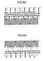
signal gate line 21, the triangularwaveform gate line 22 and thereset line 23 are each formed of a gate-level layer, while thesignal lines 8, thetriangular waveform lines 4, thepower supply lines 3 and theload lines 2 are formed of low-resistance lines formed of Al. Here, since the largest current flows through thepower supply lines 3 in particular for causing theOLED elements 24 to emit light, low-resistance lines are used for vertically extending lines. In addition, the twopower supply lines 3 are mutually connected in the horizontal direction with a line using the gate-level layer. Likewise, the twoload lines 2 are mutually connected in the horizontal direction with a line using the gate-level layer. This arrangement contributes to the prevention of degradation in picture quality which is represented by a blurring problem of images called “vertical smear” which appears in the vertical direction if a voltage drop is caused by thepower supply lines 3 or theload lines 2. - FIGS. 4A and 4B illustrate a line intersection layout above and below the pixel section by using a similar method of describing wiring. Here, FIG. 4A illustrates an area above the pixel section, while FIG. 4B illustrates an area below the pixel section. The
signal lines 8 are marked with an arrow directed toward the signal line terminals 12 (not shown in FIGS. 4A and 4B), and as is apparent from FIGS. 4A and 4B, the lines using a gate-level layer are longest in length. This is because almost no current will flow in thesignal lines 8 and therefore tolerances to wiring resistance are larger. The reason why the line length of theload lines 2 and thepower supply lines 3 using a gate-level layer is designed to be shorter in this order is the same as in the above case. - The first embodiment is not only capable of keeping the voltage drop to the minimum since the
load lines 2 and thepower supply lines 3 are brought out to many terminals provided between thesignal line terminals 12 as described above, but also ensures stabilization of the supply voltage by connecting theload lines 2 and thepower supply lines 3 between the pixels. - Now, in the first embodiment described above, it is possible to make modifications without departing from the scope of the present invention. For example, the
glass substrate 20 is used as the TFT substrate in the first embodiment, this substrate can be replaced with an other transparent insulating substrate such as a quartz substrate or a transparent plastic substrate, and further, an opaque substrate may be used when light emitted from theOLED element 24 is designed to be guided toward the top surface. - As regards each of the TFTs in the first embodiment, it is also possible to interchange the n and p conductivity types of the
input TFT 25 or thereset TFT 30 by changing the drive waveform properly. Further, as regards the inverter circuit disposed within the pixel, it is not limited to the CMOS inverter as employed in the embodiment, but it goes without saying that it is possible to make modifications such as replacing the n-channel TFT with a constant-current-source circuit, and addition of a buffer transistor in the output stage. - In addition, it is also easy to make changes in the number of pixels, and the panel size, etc. in the first embodiment. Further, the voltage at the common terminal of the
OLED element 24 is set at groun potential in this embodiment, and it is needless to say that the voltage value can be varied under specified conditions. - Also in the first embodiment, the
gate drive circuits 6 are composed of low-temperature polycrystalline Si TFTs. However, these peripheral drive circuits or part thereof may be formed of a single-crystal LSI (Large-Scale Integrated circuit) for implementations within the scope of the present invention. - The first embodiment has been explained as the
OLED element 24 used as a light emitting device. Notwithstanding the foregoing, however, it is obvious that the present invention can be realized by using other general light emitting elements including inorganic elements instead of the OLED element. - In a case where an image in color is formed by providing three separate kinds of light emitting devices, one for each of red, green and blue, it is preferable to achieve color balance by vary a light emitting area and driving voltage conditions of each of the three kinds of light emitting devices. Here, when the drive voltage conditions are to be varied, the drive voltage conditions can be adjusted by varying the voltage of the
load lines 2 and thepower supply lines 3 for the three colors, respectively, in this embodfiment. In this case, from the viewpoint of simplifying the wiring routing, it is preferred to arrange three colors in the form of stripes. However, it is obvious that mutual connections of theload lines 2 and mutual connections of thepower supply lines 3 between horizontally adjacent pixels are required for each color, and the input terminals should be divided for each color. As for the arrangement in the first embodiment where the common terminal voltage of theOLED elements 24 is set at ground potential, it is also possible to provide three separate common terminals of theOLED elements 24 for red, green and blue colors, respectively, and to drive the three kinds of light emitting devices at separate appropriate voltages, respectively. Furthermore, it is also possible to achieve a color temperature correction by adjusting the drive voltages properly, based upon display conditions and patterns to be displayed, etc. - Various changes described above can also be applied basically in similar ways to other preferred embodiments to be described subsequently in addition to the first embodiment.
- Second Embodiment
- A second embodiment according to the present invention will be described by referring to FIGS. 5 and 6.
- FIG. 5 is a configuration diagram of an OLED (Organic Light Emitting Diode) display panel in accordance with the second embodiment, and FIG. 6 is an enlarged view of a
pixel 41. Thepixels 41, each of which has anOLED element 54 serving as a pixel-light-emitting element, are arranged in a display sectionin in a matrix configuration. As shown in FIG. 6, thepixel 41 is connected to peripheries via asignal gate line 55, asignal line 48, apower supply line 43, etc. In each of thepixels 41, thesignal line 48 is connected to one terminal of astorage capacitor 92 and a gate of adrive TFT 93 via aninput TFT 91. The other terminal of thestorage capacitor 92 and a source terminal of thedrive TFT 93 are connected to thepower supply line 43. In addition, a drain terminal of thedrive TFT 93 is connected to a common grounding terminal (not shown in FIG. 6) via theOLED element 54. In the peripheral area of a pixel section, as shown in FIG. 5, thesignal gate lines 55 are connected togate drive circuits 46, thesignal lines 48 are connected to signalline terminals 52 arranged at the periphery of theglass substrate 20 separately from each other, thepower supply lines 43 are joined together above and below the pixel section and are connected topower supply terminals 51. Thepixels 41 and thegate drive circuits 46 are fabricated on theglass substrate 20 by using polycrystalline Si TFTs. - Here, FIG. 5 also illustrates 6×4 pixels only to simplify the figure, as in the case of the first embodiment, but actually, pixels of 800 (in a vertical direction)×600 (in a horizontal direction)×three colors (red, green and blue) are arranged in the second embodiment, and a large number of
signal line terminals 52 are arranged. More specifically, thesignal line terminals 52 are provided in number of 1200 above and below the pixel section, respectively, and the powersupply line terminal 51 and thecommon grounding terminals 53 are arranged alternately between thesignal line terminals 52. Thecommon grounding terminals 53 and a common grounding terminal (not shown in FIG. 5) in each of the pixels are connected to each other at grounding contact points 45. Gatedrive line groups 47 are connected to thegate drive circuits 46, and are terminated as gate driveline terminal groups 50, but are illustrated in simplified representation in FIG. 5. - The polycrystalline Si TFT structure, the OLED structure, the
gate drive circuit 6, etc. in the above-explained configuration are approximately similar to those described in the first embodiment. - Next, operation of the
pixel 41 in accordance with the second embodiment will be described by referring to FIG. 6. - When display data fed from an external source are written into the
signal line 48 via thesignal line terminal 52, the gateline drive circuit 46 successively selects thesignal gate lines 55 successively in synchronization with the above-stated writing sequence, by drive signals fed from the gate driveline terminal group 50, Thereby, the signal voltage fed to thesignal line 48 is input to thestorage capacitance 92 of a gate of thedrive TFT 93 in the pixel in the selected row via theinput TFT 91 and is retained in thestorage capacitance 92. In thepixel 41, thedrive TFT 93 is driven according to the written signal voltage, and cnsequently, theOLED element 214 emits light producing a specified luminance. Such an operation principle of thepixel 41 is similar to that of the second prior art explained earlier. - The second embodiment does not function to cancel variations in polycrystalline Si TFTs of the pixels as described in the case of the first embodiment. However, if such variations in the TFTs can be suppressed sufficiently by adequately controlling their manufacturing process, a high yield rate can be expected because of the simpler configuration of the second embodiment. Furthermore, in the second embodiment, it is possible to increase the number of both the
power supply lines 51 and thecommon grounding terminals 53 to half the number ofsignal line terminals 52, respectively, and good uniformity in luminance can be achieved for a larger display panel. - Third Embodiment
- The following will describe a third embodiment according to the present invention by referring to FIG. 7.
- FIG. 7 is a configuration diagram of an OLED display panel in accordance with the third embodiment.
- The configuration and operation of the third embodiment are basically the same as those in the second embodiment. Therefore, explanation of the configuration and operation thereof will be omitted here, and the following will explain the features of the third embodiment, that is, layouts centering upon the
signal lines 48 in relation to signalline terminals 62,power supply lines 61 andcommon grounding terminals 63. - One of the features of the third embodiment as compared with those in the second embodiment is that all the
signal lines 48 extend upward from a pixel section, and thesignal line terminals 62 are concentrated at an edge portion above the pixel section. Accordingly, an edge portion below the pixel section is provided with the powersupply line terminals 61 and thecommon grounding terminals 63 only. - For prevention of a voltage drop caused by a large current driving, it is preferable that the
power supply lines 61 and thecommon grounding terminals 63 are provided at both the top and bottom portions of the panel. However, as in the case of the third embodiment, the placement of thesignal line terminals 62 on one side of the panel provides an advantage of facilitating of mounting of the peripheral circuits on thesignal line terminals 62. - Fourth Embodiment
- The following will explain a fourth embodiment according to the present invention by referring to FIG. 8.
- FIG. 8 is a configuration diagram of an OLED display panel in accordance with the fourth embodiment.
- The configuration and operation of the third embodiment are basically the same as those in the third embodiment. Therefore, explanation of the configuration and operation thereof will be omitted here, and the following will explain the features of the fourth embodiment, that is, layouts of
signal line terminals 62 centering upon asignal line selector 64. - One of the features of the fourth embodiment as compared with those in the third embodiment is that
signal line selectors 64 are provided betweensignal lines 48 andsignal line terminals 62. Thesignal line selectors 64 are connected to thegate drive circuits 46, and also are connected to gate-selectordrive line groups 66 which are terminated as gate-selectordrive terminal groups 65, although they are indicated in simplified representation in FIG. 8. The role of thesignal selectors 64 is to supply signals to threesignal lines 48, respectively, by using a singlesignal line terminal 62 and operating a selector switch during one horizontal scanning period. Here, thesignal line selector 64 is a combination of three polycrystalline Si-TFT CMOS analog switches. - In the fourth embodiment, it is possible to reduce the number of the
signal line terminals 48 to one third by employing the above-explained configuration, and thereby to further reduce labor in mounting the circuits. - In the fourth embodiment, the number of branches of the
signal line selector 64 is arranged to be three, and as the number of branches is increased, the number of the signal line terminals can be reduced as much, but the speed of writing into thesignal lines 48 will increase accordingly. - Fifth Embodiment
- The following will explain a fifth embodiment according to the present invention by referring to FIG. 9.
- FIG. 9 is a configuration diagram of an OLED display panel in accordance with the fifth embodiment.
- The configuration and operation of the fifth embodiment are basically the same as those in the third embodiment. Therefore, explanation of the configuration and operation thereof will be omitted here, and the following explanation will focus on the features of the fifth embodiment, that is, a mounting configuration external to signal
line terminals 62, powersupply line terminals 61, andcommon grounding terminals 63. - One of the features of the fifth embodiment as compared with those in the third embodiment is that all the terminals including the power
supply line terminals 61 and thecommon grounding terminals 63 are concentrated above the pixel section, and that adrive circuit board 75 is provided externally to the terminals via aflexible cable 70. - The
drive circuit board 75 is provided with flexiblecable mounting terminals 71, and further is provided with apanel driver IC 74 and apower supply circuit 73. These are mutually connected to one another viawiring 72 on the substrate, and the signal voltages output from thepanel driver IC 74 and a supply voltage output from thepower supply circuit 73 are rearrange on thedrive circuit substrate 75 so as to be in the order corresponding to thesignal line terminals 62, the powersupply line terminals 61 and thecommon grounding terminals 63. - In the fifth embodiment, it is possible to realize a display panel more economically by using the
panel driver IC 74. Onepanel driver IC 74 is depicted in FIG. 9, but actually, sixpanel driver ICs 74 each having 400 terminals are mounted. - Sixth Embodiment
- The followin will explain a sixth embodiment according to the present invention by referring to FIG. 10.
- FIG. 10 is a configuration diagram of a personal digital assistant (PDA) 80 in accordance with the sixth embodiment.
- Compressed video data or the like are externally supplied to a wireless interface (I/F)
circuit 82 as wireless data complying with the Bluetooth specification, and the output of the wireless interface (I/F)circuit 82 is connected to adata bus 85 via an input/output (I/O)circuit 83. Further, amicroprocessor unit 84, adisplay panel controller 87, aframe memory 86 and others are connected to thedata bus 85. In addition, an output of thedisplay panel controller 87 is input to anOLED display panel 81 and a power supply circuit 88, and further, the output from the power supply circuit 88 is also input to theOLED display panel 81. ThePDA 30 is provided with anotherpower supply 89. TheOLED display panel 81 has the same configuration and perform the same operation as those of the aforementioned first embodiment, and the explanation of the internal configuration as well as the operation is omitted here. - In the followin, operation of the sixth embodiment will be described. First, the wireless I/
F circuit 82 receives compressed video data from the outside based upon a command, and transfers the video data to both themicroprocessor unit 84 and theframe memory 86 via the I/O circuit 83. Upon receiving a command from a user, themicroprocessor unit 84 drives thePDA 80 as required, and executes decoding, signal processing and information display of the compressed video data. The video data having been subjected to signal processing are temporarily stored in theframe memory 86. - Here, when the
microprocessor unit 84 issues a display command, the video data are fed from theframe memory 86 to theOLED display panel 81 via thedisplay panel controller 87 and the voltage supply circuit 88, and thereby theOLED display panel 81 displays the input video data in real time. At this time, thedisplay panel controller 87 also outputs a specified timing pulse and a triangular waveform voltage required for displaying the video image. The sequence in which theOLED display panel 81 uses these signals to display in real time display data derived from six-bit video data on the pixel section is the same as that described in the first embodiment. Incidentally, thepower supply 89 contains a secondary battery to supply power for driving theentire PDA 80. - According to the present embodiment, it is possible to provide the
PDA 80 which exhibits superior uniformity in display luminance and has a large display area. - In the sixth embodiment, the OLED display panel described in the first embodiment is employed. However, it is obvious that any other types of display panels described in the other embodiments according to the present invention may be used.
- According to the present invention, it is possible to provide an image display apparatus which exhibits superior uniformity in display luminance over a relatively large screen area.
Claims (16)
Applications Claiming Priority (2)
| Application Number | Priority Date | Filing Date | Title |
|---|---|---|---|
| JP2002142369A JP4165120B2 (en) | 2002-05-17 | 2002-05-17 | Image display device |
| JP2002-142369 | 2002-05-17 |
Publications (2)
| Publication Number | Publication Date |
|---|---|
| US20040004591A1 true US20040004591A1 (en) | 2004-01-08 |
| US7733309B2 US7733309B2 (en) | 2010-06-08 |
Family
ID=29702671
Family Applications (1)
| Application Number | Title | Priority Date | Filing Date |
|---|---|---|---|
| US10/438,841 Active 2027-02-19 US7733309B2 (en) | 2002-05-17 | 2003-05-16 | Image display apparatus |
Country Status (4)
| Country | Link |
|---|---|
| US (1) | US7733309B2 (en) |
| JP (1) | JP4165120B2 (en) |
| KR (1) | KR100965646B1 (en) |
| TW (1) | TWI272668B (en) |
Cited By (14)
| Publication number | Priority date | Publication date | Assignee | Title |
|---|---|---|---|---|
| US20030214469A1 (en) * | 2002-05-17 | 2003-11-20 | Hiroshi Kageyama | Image display apparatus |
| US20050139841A1 (en) * | 2003-12-30 | 2005-06-30 | Lg.Philips Lcd Co., Ltd. | Organic electroluminescent display device |
| US20050156514A1 (en) * | 2003-12-27 | 2005-07-21 | Lg.Philips Lcd Co., Ltd. | Active matrix organic electroluminescent display device and method of fabricating the same |
| US20050280737A1 (en) * | 2004-06-17 | 2005-12-22 | Isao Takayanagi | Operation stablized pixel bias circuit |
| US20060145969A1 (en) * | 2003-06-26 | 2006-07-06 | Koninklijke Philips Electronics N.V. | Light emitting display devices |
| US20070176886A1 (en) * | 2006-01-31 | 2007-08-02 | Norikazu Nagasawa | Information processing apparatus and luminance control method |
| US20070182672A1 (en) * | 2004-03-10 | 2007-08-09 | Koninklijke Philips Electronics, N.V. | Active matrix display with reduction of power onsumption |
| EP1817764A1 (en) * | 2004-11-30 | 2007-08-15 | Semiconductor Energy Laboratory Co., Ltd. | Display device and driving method thereof, semiconductor device, and electronic apparatus |
| US20080100543A1 (en) * | 2006-10-13 | 2008-05-01 | Naruhiko Kasai | Display device |
| US20080158111A1 (en) * | 2006-12-27 | 2008-07-03 | Sony Corporation | Image display device |
| US20090109147A1 (en) * | 2007-10-29 | 2009-04-30 | Sungcheon Park | Organic light emitting display and power supply method thereof |
| US20130021312A1 (en) * | 2010-04-02 | 2013-01-24 | Sharp Kabushiki Kaisha | Display device and drive method therefor |
| TWI415068B (en) * | 2007-11-09 | 2013-11-11 | Sony Corp | Electroluminescent display panel and electronic device |
| EP4047653A4 (en) * | 2019-10-14 | 2022-11-23 | BOE Technology Group Co., Ltd. | Array substrate and display device |
Families Citing this family (19)
| Publication number | Priority date | Publication date | Assignee | Title |
|---|---|---|---|---|
| JP4780950B2 (en) * | 2003-11-21 | 2011-09-28 | 株式会社半導体エネルギー研究所 | Display device |
| TWI362231B (en) * | 2003-11-21 | 2012-04-11 | Semiconductor Energy Lab | Display device |
| KR100578911B1 (en) | 2003-11-26 | 2006-05-11 | 삼성에스디아이 주식회사 | Current demultiplexing device and current programming display device using the same |
| KR100578913B1 (en) * | 2003-11-27 | 2006-05-11 | 삼성에스디아이 주식회사 | Display device using demultiplexer and driving method thereof |
| KR100578914B1 (en) | 2003-11-27 | 2006-05-11 | 삼성에스디아이 주식회사 | Display device using demultiplexer |
| KR100589381B1 (en) | 2003-11-27 | 2006-06-14 | 삼성에스디아이 주식회사 | Display device using demultiplexer and driving method thereof |
| KR100589376B1 (en) | 2003-11-27 | 2006-06-14 | 삼성에스디아이 주식회사 | Light emitting display device using demultiplexer |
| JP3985788B2 (en) | 2004-01-22 | 2007-10-03 | セイコーエプソン株式会社 | Electro-optical device and electronic apparatus |
| KR100600350B1 (en) | 2004-05-15 | 2006-07-14 | 삼성에스디아이 주식회사 | demultiplexer and Organic electroluminescent display using thereof |
| KR100622217B1 (en) | 2004-05-25 | 2006-09-08 | 삼성에스디아이 주식회사 | Organic electroluminscent display and demultiplexer |
| US7646367B2 (en) | 2005-01-21 | 2010-01-12 | Semiconductor Energy Laboratory Co., Ltd. | Semiconductor device, display device and electronic apparatus |
| US8681077B2 (en) * | 2005-03-18 | 2014-03-25 | Semiconductor Energy Laboratory Co., Ltd. | Semiconductor device, and display device, driving method and electronic apparatus thereof |
| JP5023271B2 (en) * | 2006-02-27 | 2012-09-12 | 株式会社ジャパンディスプレイイースト | Organic EL display device |
| JP2007232795A (en) | 2006-02-27 | 2007-09-13 | Hitachi Displays Ltd | Organic el display device |
| KR100748335B1 (en) | 2006-05-09 | 2007-08-09 | 삼성에스디아이 주식회사 | Data driver and organic light emitting display using the same |
| KR100916911B1 (en) * | 2008-01-18 | 2009-09-09 | 삼성모바일디스플레이주식회사 | Organic Light Emitting Display Device |
| KR100907415B1 (en) * | 2008-01-18 | 2009-07-10 | 삼성모바일디스플레이주식회사 | Organic light emitting display device |
| CN108281107A (en) * | 2018-01-26 | 2018-07-13 | 京东方科技集团股份有限公司 | It is a kind of display color of image compensation method and splicing display device |
| CN109458107B (en) * | 2018-12-21 | 2023-08-22 | 绍兴市上虞区幻想动力机器人科技有限公司 | Unidirectional glass utilizing human eye vision residues |
Citations (9)
| Publication number | Priority date | Publication date | Assignee | Title |
|---|---|---|---|---|
| US4468659A (en) * | 1980-08-25 | 1984-08-28 | Sharp Kabushiki Kaisha | Electroluminescent display panel assembly |
| US20010048408A1 (en) * | 2000-02-22 | 2001-12-06 | Jun Koyama | Image display device and driver circuit therefor |
| US6528950B2 (en) * | 2000-04-06 | 2003-03-04 | Semiconductor Energy Laboratory Co., Ltd. | Electronic device and driving method |
| US6541910B2 (en) * | 2000-04-06 | 2003-04-01 | Seiko Epson Corporation | Organic el display |
| US6714178B2 (en) * | 2000-05-12 | 2004-03-30 | Semiconductor Energy Laboratory Co., Ltd. | Display device |
| US6747617B1 (en) * | 1999-11-18 | 2004-06-08 | Nec Corporation | Drive circuit for an organic EL apparatus |
| US6771258B2 (en) * | 2000-12-11 | 2004-08-03 | Seiko Epson Corporation | Semiconductor device |
| US7164155B2 (en) * | 2002-05-15 | 2007-01-16 | Semiconductor Energy Laboratory Co., Ltd. | Light emitting device |
| US7557779B2 (en) * | 2003-06-13 | 2009-07-07 | Semiconductor Energy Laboratory Co., Ltd. | Display device |
Family Cites Families (6)
| Publication number | Priority date | Publication date | Assignee | Title |
|---|---|---|---|---|
| JP2001092412A (en) * | 1999-09-17 | 2001-04-06 | Pioneer Electronic Corp | Active matrix type display device |
| JP2001109395A (en) * | 1999-10-01 | 2001-04-20 | Sanyo Electric Co Ltd | El display device |
| JP2001312255A (en) * | 2000-05-01 | 2001-11-09 | Toshiba Corp | Display device |
| JP2002032037A (en) * | 2000-05-12 | 2002-01-31 | Semiconductor Energy Lab Co Ltd | Display device |
| JP4593740B2 (en) * | 2000-07-28 | 2010-12-08 | ルネサスエレクトロニクス株式会社 | Display device |
| JP3660216B2 (en) * | 2000-08-22 | 2005-06-15 | シャープ株式会社 | Matrix type display device |
-
2002
- 2002-05-17 JP JP2002142369A patent/JP4165120B2/en not_active Expired - Lifetime
-
2003
- 2003-03-25 KR KR1020030018354A patent/KR100965646B1/en active IP Right Grant
- 2003-04-17 TW TW092108915A patent/TWI272668B/en not_active IP Right Cessation
- 2003-05-16 US US10/438,841 patent/US7733309B2/en active Active
Patent Citations (9)
| Publication number | Priority date | Publication date | Assignee | Title |
|---|---|---|---|---|
| US4468659A (en) * | 1980-08-25 | 1984-08-28 | Sharp Kabushiki Kaisha | Electroluminescent display panel assembly |
| US6747617B1 (en) * | 1999-11-18 | 2004-06-08 | Nec Corporation | Drive circuit for an organic EL apparatus |
| US20010048408A1 (en) * | 2000-02-22 | 2001-12-06 | Jun Koyama | Image display device and driver circuit therefor |
| US6528950B2 (en) * | 2000-04-06 | 2003-03-04 | Semiconductor Energy Laboratory Co., Ltd. | Electronic device and driving method |
| US6541910B2 (en) * | 2000-04-06 | 2003-04-01 | Seiko Epson Corporation | Organic el display |
| US6714178B2 (en) * | 2000-05-12 | 2004-03-30 | Semiconductor Energy Laboratory Co., Ltd. | Display device |
| US6771258B2 (en) * | 2000-12-11 | 2004-08-03 | Seiko Epson Corporation | Semiconductor device |
| US7164155B2 (en) * | 2002-05-15 | 2007-01-16 | Semiconductor Energy Laboratory Co., Ltd. | Light emitting device |
| US7557779B2 (en) * | 2003-06-13 | 2009-07-07 | Semiconductor Energy Laboratory Co., Ltd. | Display device |
Cited By (35)
| Publication number | Priority date | Publication date | Assignee | Title |
|---|---|---|---|---|
| US20030214469A1 (en) * | 2002-05-17 | 2003-11-20 | Hiroshi Kageyama | Image display apparatus |
| US7379044B2 (en) | 2002-05-17 | 2008-05-27 | Hitachi, Ltd. | Image display apparatus |
| US20070222732A1 (en) * | 2002-05-17 | 2007-09-27 | Hiroshi Kageyama | Image display apparatus |
| US7221343B2 (en) * | 2002-05-17 | 2007-05-22 | Hitachi, Ltd. | Image display apparatus |
| US20060145969A1 (en) * | 2003-06-26 | 2006-07-06 | Koninklijke Philips Electronics N.V. | Light emitting display devices |
| US8847859B2 (en) * | 2003-06-26 | 2014-09-30 | Koninklijke Philips N.V. | Light emitting display devices |
| US20050156514A1 (en) * | 2003-12-27 | 2005-07-21 | Lg.Philips Lcd Co., Ltd. | Active matrix organic electroluminescent display device and method of fabricating the same |
| US7446741B2 (en) * | 2003-12-27 | 2008-11-04 | Lg Display Co., Ltd. | Active matrix organic electroluminescent display device and method of fabricating the same |
| US7348605B2 (en) * | 2003-12-30 | 2008-03-25 | Lg.Philips Lcd Co., Ltd. | Organic electroluminescent display device |
| US20050139841A1 (en) * | 2003-12-30 | 2005-06-30 | Lg.Philips Lcd Co., Ltd. | Organic electroluminescent display device |
| US20080136323A1 (en) * | 2003-12-30 | 2008-06-12 | Lg Philips Lcd Co., Ltd. | Organic electroluminescent display device |
| US7764328B2 (en) | 2003-12-30 | 2010-07-27 | Lg Display Co., Ltd. | Organic electroluminescent display device |
| US20070182672A1 (en) * | 2004-03-10 | 2007-08-09 | Koninklijke Philips Electronics, N.V. | Active matrix display with reduction of power onsumption |
| US7777738B2 (en) * | 2004-03-10 | 2010-08-17 | Koninklijke Philips Electronics N.V. | Active matrix display with reduction of power consumption |
| US20050280737A1 (en) * | 2004-06-17 | 2005-12-22 | Isao Takayanagi | Operation stablized pixel bias circuit |
| US7825982B2 (en) * | 2004-06-17 | 2010-11-02 | Aptina Imaging Corporation | Operation stabilized pixel bias circuit |
| US20090051674A1 (en) * | 2004-11-30 | 2009-02-26 | Hajime Kimura | Display device and driving method thereof, semiconductor device, and electronic apparatus |
| US8426866B2 (en) | 2004-11-30 | 2013-04-23 | Semiconductor Energy Laboratory Co., Ltd. | Display device and driving method thereof, semiconductor device, and electronic apparatus |
| EP1817764A4 (en) * | 2004-11-30 | 2009-08-26 | Semiconductor Energy Lab | Display device and driving method thereof, semiconductor device, and electronic apparatus |
| EP1817764A1 (en) * | 2004-11-30 | 2007-08-15 | Semiconductor Energy Laboratory Co., Ltd. | Display device and driving method thereof, semiconductor device, and electronic apparatus |
| US20070176886A1 (en) * | 2006-01-31 | 2007-08-02 | Norikazu Nagasawa | Information processing apparatus and luminance control method |
| US7872632B2 (en) * | 2006-01-31 | 2011-01-18 | Kabushiki Kaisha Toshiba | Information processing apparatus and luminance control method |
| US20080100543A1 (en) * | 2006-10-13 | 2008-05-01 | Naruhiko Kasai | Display device |
| US7982697B2 (en) * | 2006-10-13 | 2011-07-19 | Hitachi Displays, Ltd. | Display device mounted with self-luminous element |
| US8493321B2 (en) * | 2006-12-27 | 2013-07-23 | Sony Corporation | Image display device having a thin display panel |
| US20080158111A1 (en) * | 2006-12-27 | 2008-07-03 | Sony Corporation | Image display device |
| US20090109147A1 (en) * | 2007-10-29 | 2009-04-30 | Sungcheon Park | Organic light emitting display and power supply method thereof |
| US9041626B2 (en) * | 2007-10-29 | 2015-05-26 | Samsung Display Co., Ltd. | Organic light emitting display and power supply method thereof |
| TWI415068B (en) * | 2007-11-09 | 2013-11-11 | Sony Corp | Electroluminescent display panel and electronic device |
| TWI560675B (en) * | 2007-11-09 | 2016-12-01 | Sony Corp | Electroluminescent display panel and electronic device |
| TWI588800B (en) * | 2007-11-09 | 2017-06-21 | 新力股份有限公司 | Electroluminescent display panel and electronic device |
| US20130021312A1 (en) * | 2010-04-02 | 2013-01-24 | Sharp Kabushiki Kaisha | Display device and drive method therefor |
| US9361826B2 (en) * | 2010-04-02 | 2016-06-07 | Sharp Kabushiki Kaisha | Display device and drive method therefor |
| EP4047653A4 (en) * | 2019-10-14 | 2022-11-23 | BOE Technology Group Co., Ltd. | Array substrate and display device |
| US11551609B2 (en) | 2019-10-14 | 2023-01-10 | Chengdu Boe Optoelectronics Technology Co., Ltd. | Array substrate and display device |
Also Published As
| Publication number | Publication date |
|---|---|
| JP4165120B2 (en) | 2008-10-15 |
| TW200410323A (en) | 2004-06-16 |
| US7733309B2 (en) | 2010-06-08 |
| JP2003330386A (en) | 2003-11-19 |
| KR20030089417A (en) | 2003-11-21 |
| TWI272668B (en) | 2007-02-01 |
| KR100965646B1 (en) | 2010-06-23 |
Similar Documents
| Publication | Publication Date | Title |
|---|---|---|
| US7733309B2 (en) | Image display apparatus | |
| KR101060017B1 (en) | Image display | |
| JP3772889B2 (en) | Electro-optical device and driving device thereof | |
| JP3877049B2 (en) | Image display apparatus and driving method thereof | |
| KR100519686B1 (en) | Active matrix display panel and image display device adapting same | |
| US6738034B2 (en) | Picture image display device and method of driving the same | |
| JP4027614B2 (en) | Display device | |
| US7982694B2 (en) | Display apparatus and drive control method | |
| US6801180B2 (en) | Display device | |
| TWI508044B (en) | Display device and electronic apparatus, and driving method of display panel | |
| JP2011112723A (en) | Display device, method of driving the same and electronic equipment | |
| JP2010266848A (en) | El display device and driving method thereof | |
| CN113096600B (en) | Folding display panel, folding display device, driving method of folding display device and electronic equipment | |
| KR20070057020A (en) | Image display device | |
| JP4039441B2 (en) | Electro-optical device and electronic apparatus | |
| KR20200020328A (en) | Organic Light Emitting Diode display panel and Organic Light Emitting Diode display device using the same | |
| JP6417608B2 (en) | Image display device and image display device driving method. | |
| JP2012047894A (en) | Display device | |
| US20060290622A1 (en) | Active matrix display device and method of driving active matrix display device | |
| KR102203773B1 (en) | Display panel and Organic Light Emitting Diode display device using the same | |
| JP7362889B2 (en) | display device | |
| JP4842537B2 (en) | Display device | |
| WO2024088027A1 (en) | Display substrate and driving method therefor, and display apparatus | |
| JP5201712B2 (en) | Display device | |
| JP5442678B2 (en) | Display device |
Legal Events
| Date | Code | Title | Description |
|---|---|---|---|
| AS | Assignment |
Owner name: HITACHI, LTD., JAPAN Free format text: ASSIGNMENT OF ASSIGNORS INTEREST;ASSIGNORS:AKIMOTO, HAJIME;SATO, TOSHIHIRO;MIKAMI, YOSHIROU;AND OTHERS;REEL/FRAME:014087/0621;SIGNING DATES FROM 20030319 TO 20030325 Owner name: HITACHI, LTD.,JAPAN Free format text: ASSIGNMENT OF ASSIGNORS INTEREST;ASSIGNORS:AKIMOTO, HAJIME;SATO, TOSHIHIRO;MIKAMI, YOSHIROU;AND OTHERS;SIGNING DATES FROM 20030319 TO 20030325;REEL/FRAME:014087/0621 |
|
| STCF | Information on status: patent grant |
Free format text: PATENTED CASE |
|
| AS | Assignment |
Owner name: HITACHI DISPLAYS, LTD., JAPAN Free format text: ASSIGNMENT OF ASSIGNORS INTEREST;ASSIGNOR:HITACHI, LTD.;REEL/FRAME:025008/0380 Effective date: 20100823 |
|
| FEPP | Fee payment procedure |
Free format text: PAYOR NUMBER ASSIGNED (ORIGINAL EVENT CODE: ASPN); ENTITY STATUS OF PATENT OWNER: LARGE ENTITY |
|
| AS | Assignment |
Owner name: IPS ALPHA SUPPORT CO., LTD., JAPAN Free format text: COMPANY SPLIT PLAN TRANSFERRING FIFTY (50) PERCENT SHARE OF PATENTS AND PATENT APPLICATIONS;ASSIGNOR:HITACHI DISPLAYS, LTD.;REEL/FRAME:027362/0466 Effective date: 20100630 Owner name: PANASONIC LIQUID CRYSTAL DISPLAY CO., LTD., JAPAN Free format text: MERGER/CHANGE OF NAME;ASSIGNOR:IPS ALPHA SUPPORT CO., LTD.;REEL/FRAME:027363/0315 Effective date: 20101001 Owner name: HITACHI DISPLAYS, LTD., JAPAN Free format text: COMPANY SPLIT PLAN TRANSFERRING ONE HUNDRED (100) PERCENT SHARE OF PATENT AND PATENT APPLICATIONS;ASSIGNOR:HITACHI, LTD.;REEL/FRAME:027362/0612 Effective date: 20021001 |
|
| FPAY | Fee payment |
Year of fee payment: 4 |
|
| MAFP | Maintenance fee payment |
Free format text: PAYMENT OF MAINTENANCE FEE, 8TH YEAR, LARGE ENTITY (ORIGINAL EVENT CODE: M1552) Year of fee payment: 8 |
|
| AS | Assignment |
Owner name: SAMSUNG DISPLAY CO., LTD., KOREA, REPUBLIC OF Free format text: ASSIGNMENT OF ASSIGNORS INTEREST;ASSIGNORS:PANASONIC LIQUID CRYSTAL DISPLAY CO., LTD.;JAPAN DISPLAY INC.;SIGNING DATES FROM 20180731 TO 20180802;REEL/FRAME:046988/0801 |
|
| MAFP | Maintenance fee payment |
Free format text: PAYMENT OF MAINTENANCE FEE, 12TH YEAR, LARGE ENTITY (ORIGINAL EVENT CODE: M1553); ENTITY STATUS OF PATENT OWNER: LARGE ENTITY Year of fee payment: 12 |