US20040134603A1 - Method and apparatus for curing adhesive between substrates, and disc substrate bonding apparatus - Google Patents
Method and apparatus for curing adhesive between substrates, and disc substrate bonding apparatus Download PDFInfo
- Publication number
- US20040134603A1 US20040134603A1 US10/622,357 US62235703A US2004134603A1 US 20040134603 A1 US20040134603 A1 US 20040134603A1 US 62235703 A US62235703 A US 62235703A US 2004134603 A1 US2004134603 A1 US 2004134603A1
- Authority
- US
- United States
- Prior art keywords
- adhesive
- substrates
- light emitting
- disc substrates
- disc
- Prior art date
- Legal status (The legal status is an assumption and is not a legal conclusion. Google has not performed a legal analysis and makes no representation as to the accuracy of the status listed.)
- Abandoned
Links
- 239000000758 substrate Substances 0.000 title claims abstract description 478
- 239000000853 adhesive Substances 0.000 title claims abstract description 236
- 230000001070 adhesive effect Effects 0.000 title claims abstract description 236
- 238000000034 method Methods 0.000 title claims description 32
- 230000007246 mechanism Effects 0.000 claims abstract description 161
- 239000004065 semiconductor Substances 0.000 claims abstract description 103
- 239000012790 adhesive layer Substances 0.000 claims description 53
- 238000012546 transfer Methods 0.000 claims description 42
- 230000003287 optical effect Effects 0.000 claims description 36
- NJPPVKZQTLUDBO-UHFFFAOYSA-N novaluron Chemical compound C1=C(Cl)C(OC(F)(F)C(OC(F)(F)F)F)=CC=C1NC(=O)NC(=O)C1=C(F)C=CC=C1F NJPPVKZQTLUDBO-UHFFFAOYSA-N 0.000 claims description 34
- 239000010410 layer Substances 0.000 claims description 24
- 239000007789 gas Substances 0.000 claims description 21
- 230000008569 process Effects 0.000 claims description 12
- 239000002826 coolant Substances 0.000 claims description 6
- 238000001816 cooling Methods 0.000 claims description 6
- 238000009826 distribution Methods 0.000 claims description 6
- QVGXLLKOCUKJST-UHFFFAOYSA-N atomic oxygen Chemical compound [O] QVGXLLKOCUKJST-UHFFFAOYSA-N 0.000 claims description 3
- 239000001301 oxygen Substances 0.000 claims description 3
- 229910052760 oxygen Inorganic materials 0.000 claims description 3
- 230000001627 detrimental effect Effects 0.000 description 10
- 238000004519 manufacturing process Methods 0.000 description 9
- 229920000515 polycarbonate Polymers 0.000 description 8
- 239000004417 polycarbonate Substances 0.000 description 8
- 230000035945 sensitivity Effects 0.000 description 7
- 230000000694 effects Effects 0.000 description 6
- 229920002379 silicone rubber Polymers 0.000 description 6
- 238000007664 blowing Methods 0.000 description 5
- 239000011521 glass Substances 0.000 description 5
- 238000005192 partition Methods 0.000 description 5
- 230000005855 radiation Effects 0.000 description 5
- 238000003892 spreading Methods 0.000 description 5
- 230000007480 spreading Effects 0.000 description 5
- 238000006243 chemical reaction Methods 0.000 description 4
- 239000010408 film Substances 0.000 description 4
- 230000033001 locomotion Effects 0.000 description 4
- IJGRMHOSHXDMSA-UHFFFAOYSA-N Atomic nitrogen Chemical compound N#N IJGRMHOSHXDMSA-UHFFFAOYSA-N 0.000 description 3
- 229910052782 aluminium Inorganic materials 0.000 description 3
- XAGFODPZIPBFFR-UHFFFAOYSA-N aluminium Chemical compound [Al] XAGFODPZIPBFFR-UHFFFAOYSA-N 0.000 description 3
- 230000005540 biological transmission Effects 0.000 description 3
- 238000010276 construction Methods 0.000 description 3
- 229910001873 dinitrogen Inorganic materials 0.000 description 3
- 230000020169 heat generation Effects 0.000 description 3
- 239000000463 material Substances 0.000 description 3
- 230000001681 protective effect Effects 0.000 description 3
- 229910052724 xenon Inorganic materials 0.000 description 3
- FHNFHKCVQCLJFQ-UHFFFAOYSA-N xenon atom Chemical compound [Xe] FHNFHKCVQCLJFQ-UHFFFAOYSA-N 0.000 description 3
- XKRFYHLGVUSROY-UHFFFAOYSA-N Argon Chemical compound [Ar] XKRFYHLGVUSROY-UHFFFAOYSA-N 0.000 description 2
- 238000010521 absorption reaction Methods 0.000 description 2
- 238000013459 approach Methods 0.000 description 2
- 239000011261 inert gas Substances 0.000 description 2
- 239000000203 mixture Substances 0.000 description 2
- 238000006116 polymerization reaction Methods 0.000 description 2
- 238000003825 pressing Methods 0.000 description 2
- 239000011347 resin Substances 0.000 description 2
- 229920005989 resin Polymers 0.000 description 2
- 230000035939 shock Effects 0.000 description 2
- 239000010409 thin film Substances 0.000 description 2
- 229910052779 Neodymium Inorganic materials 0.000 description 1
- 239000002313 adhesive film Substances 0.000 description 1
- 229910052786 argon Inorganic materials 0.000 description 1
- 230000001174 ascending effect Effects 0.000 description 1
- 230000008901 benefit Effects 0.000 description 1
- 239000003990 capacitor Substances 0.000 description 1
- 238000007796 conventional method Methods 0.000 description 1
- 238000013016 damping Methods 0.000 description 1
- 230000006866 deterioration Effects 0.000 description 1
- 230000005684 electric field Effects 0.000 description 1
- 230000007613 environmental effect Effects 0.000 description 1
- 239000012530 fluid Substances 0.000 description 1
- 230000006870 function Effects 0.000 description 1
- 230000017525 heat dissipation Effects 0.000 description 1
- 239000001307 helium Substances 0.000 description 1
- 229910052734 helium Inorganic materials 0.000 description 1
- SWQJXJOGLNCZEY-UHFFFAOYSA-N helium atom Chemical compound [He] SWQJXJOGLNCZEY-UHFFFAOYSA-N 0.000 description 1
- 230000001678 irradiating effect Effects 0.000 description 1
- 230000031700 light absorption Effects 0.000 description 1
- 239000007788 liquid Substances 0.000 description 1
- 238000012423 maintenance Methods 0.000 description 1
- 229910052751 metal Inorganic materials 0.000 description 1
- 239000002184 metal Substances 0.000 description 1
- 229910001507 metal halide Inorganic materials 0.000 description 1
- 150000005309 metal halides Chemical class 0.000 description 1
- QEFYFXOXNSNQGX-UHFFFAOYSA-N neodymium atom Chemical compound [Nd] QEFYFXOXNSNQGX-UHFFFAOYSA-N 0.000 description 1
- 229910052754 neon Inorganic materials 0.000 description 1
- GKAOGPIIYCISHV-UHFFFAOYSA-N neon atom Chemical compound [Ne] GKAOGPIIYCISHV-UHFFFAOYSA-N 0.000 description 1
- 238000009987 spinning Methods 0.000 description 1
- 239000012780 transparent material Substances 0.000 description 1
- 230000000007 visual effect Effects 0.000 description 1
Images


Classifications
-
- B—PERFORMING OPERATIONS; TRANSPORTING
- B29—WORKING OF PLASTICS; WORKING OF SUBSTANCES IN A PLASTIC STATE IN GENERAL
- B29C—SHAPING OR JOINING OF PLASTICS; SHAPING OF MATERIAL IN A PLASTIC STATE, NOT OTHERWISE PROVIDED FOR; AFTER-TREATMENT OF THE SHAPED PRODUCTS, e.g. REPAIRING
- B29C65/00—Joining or sealing of preformed parts, e.g. welding of plastics materials; Apparatus therefor
- B29C65/02—Joining or sealing of preformed parts, e.g. welding of plastics materials; Apparatus therefor by heating, with or without pressure
- B29C65/14—Joining or sealing of preformed parts, e.g. welding of plastics materials; Apparatus therefor by heating, with or without pressure using wave energy, i.e. electromagnetic radiation, or particle radiation
- B29C65/1429—Joining or sealing of preformed parts, e.g. welding of plastics materials; Apparatus therefor by heating, with or without pressure using wave energy, i.e. electromagnetic radiation, or particle radiation characterised by the way of heating the interface
- B29C65/1464—Joining or sealing of preformed parts, e.g. welding of plastics materials; Apparatus therefor by heating, with or without pressure using wave energy, i.e. electromagnetic radiation, or particle radiation characterised by the way of heating the interface making use of several radiators
- B29C65/1467—Joining or sealing of preformed parts, e.g. welding of plastics materials; Apparatus therefor by heating, with or without pressure using wave energy, i.e. electromagnetic radiation, or particle radiation characterised by the way of heating the interface making use of several radiators at the same time, i.e. simultaneous welding
-
- B—PERFORMING OPERATIONS; TRANSPORTING
- B29—WORKING OF PLASTICS; WORKING OF SUBSTANCES IN A PLASTIC STATE IN GENERAL
- B29C—SHAPING OR JOINING OF PLASTICS; SHAPING OF MATERIAL IN A PLASTIC STATE, NOT OTHERWISE PROVIDED FOR; AFTER-TREATMENT OF THE SHAPED PRODUCTS, e.g. REPAIRING
- B29C65/00—Joining or sealing of preformed parts, e.g. welding of plastics materials; Apparatus therefor
- B29C65/02—Joining or sealing of preformed parts, e.g. welding of plastics materials; Apparatus therefor by heating, with or without pressure
- B29C65/14—Joining or sealing of preformed parts, e.g. welding of plastics materials; Apparatus therefor by heating, with or without pressure using wave energy, i.e. electromagnetic radiation, or particle radiation
- B29C65/1403—Joining or sealing of preformed parts, e.g. welding of plastics materials; Apparatus therefor by heating, with or without pressure using wave energy, i.e. electromagnetic radiation, or particle radiation characterised by the type of electromagnetic or particle radiation
- B29C65/1406—Ultraviolet [UV] radiation
-
- B—PERFORMING OPERATIONS; TRANSPORTING
- B29—WORKING OF PLASTICS; WORKING OF SUBSTANCES IN A PLASTIC STATE IN GENERAL
- B29C—SHAPING OR JOINING OF PLASTICS; SHAPING OF MATERIAL IN A PLASTIC STATE, NOT OTHERWISE PROVIDED FOR; AFTER-TREATMENT OF THE SHAPED PRODUCTS, e.g. REPAIRING
- B29C65/00—Joining or sealing of preformed parts, e.g. welding of plastics materials; Apparatus therefor
- B29C65/02—Joining or sealing of preformed parts, e.g. welding of plastics materials; Apparatus therefor by heating, with or without pressure
- B29C65/14—Joining or sealing of preformed parts, e.g. welding of plastics materials; Apparatus therefor by heating, with or without pressure using wave energy, i.e. electromagnetic radiation, or particle radiation
- B29C65/1429—Joining or sealing of preformed parts, e.g. welding of plastics materials; Apparatus therefor by heating, with or without pressure using wave energy, i.e. electromagnetic radiation, or particle radiation characterised by the way of heating the interface
- B29C65/1435—Joining or sealing of preformed parts, e.g. welding of plastics materials; Apparatus therefor by heating, with or without pressure using wave energy, i.e. electromagnetic radiation, or particle radiation characterised by the way of heating the interface at least passing through one of the parts to be joined, i.e. transmission welding
-
- B—PERFORMING OPERATIONS; TRANSPORTING
- B29—WORKING OF PLASTICS; WORKING OF SUBSTANCES IN A PLASTIC STATE IN GENERAL
- B29C—SHAPING OR JOINING OF PLASTICS; SHAPING OF MATERIAL IN A PLASTIC STATE, NOT OTHERWISE PROVIDED FOR; AFTER-TREATMENT OF THE SHAPED PRODUCTS, e.g. REPAIRING
- B29C65/00—Joining or sealing of preformed parts, e.g. welding of plastics materials; Apparatus therefor
- B29C65/02—Joining or sealing of preformed parts, e.g. welding of plastics materials; Apparatus therefor by heating, with or without pressure
- B29C65/14—Joining or sealing of preformed parts, e.g. welding of plastics materials; Apparatus therefor by heating, with or without pressure using wave energy, i.e. electromagnetic radiation, or particle radiation
- B29C65/1429—Joining or sealing of preformed parts, e.g. welding of plastics materials; Apparatus therefor by heating, with or without pressure using wave energy, i.e. electromagnetic radiation, or particle radiation characterised by the way of heating the interface
- B29C65/1454—Joining or sealing of preformed parts, e.g. welding of plastics materials; Apparatus therefor by heating, with or without pressure using wave energy, i.e. electromagnetic radiation, or particle radiation characterised by the way of heating the interface scanning at least one of the parts to be joined
-
- B—PERFORMING OPERATIONS; TRANSPORTING
- B29—WORKING OF PLASTICS; WORKING OF SUBSTANCES IN A PLASTIC STATE IN GENERAL
- B29C—SHAPING OR JOINING OF PLASTICS; SHAPING OF MATERIAL IN A PLASTIC STATE, NOT OTHERWISE PROVIDED FOR; AFTER-TREATMENT OF THE SHAPED PRODUCTS, e.g. REPAIRING
- B29C65/00—Joining or sealing of preformed parts, e.g. welding of plastics materials; Apparatus therefor
- B29C65/02—Joining or sealing of preformed parts, e.g. welding of plastics materials; Apparatus therefor by heating, with or without pressure
- B29C65/14—Joining or sealing of preformed parts, e.g. welding of plastics materials; Apparatus therefor by heating, with or without pressure using wave energy, i.e. electromagnetic radiation, or particle radiation
- B29C65/1477—Joining or sealing of preformed parts, e.g. welding of plastics materials; Apparatus therefor by heating, with or without pressure using wave energy, i.e. electromagnetic radiation, or particle radiation making use of an absorber or impact modifier
- B29C65/1483—Joining or sealing of preformed parts, e.g. welding of plastics materials; Apparatus therefor by heating, with or without pressure using wave energy, i.e. electromagnetic radiation, or particle radiation making use of an absorber or impact modifier coated on the article
-
- B—PERFORMING OPERATIONS; TRANSPORTING
- B29—WORKING OF PLASTICS; WORKING OF SUBSTANCES IN A PLASTIC STATE IN GENERAL
- B29C—SHAPING OR JOINING OF PLASTICS; SHAPING OF MATERIAL IN A PLASTIC STATE, NOT OTHERWISE PROVIDED FOR; AFTER-TREATMENT OF THE SHAPED PRODUCTS, e.g. REPAIRING
- B29C65/00—Joining or sealing of preformed parts, e.g. welding of plastics materials; Apparatus therefor
- B29C65/48—Joining or sealing of preformed parts, e.g. welding of plastics materials; Apparatus therefor using adhesives, i.e. using supplementary joining material; solvent bonding
- B29C65/4805—Joining or sealing of preformed parts, e.g. welding of plastics materials; Apparatus therefor using adhesives, i.e. using supplementary joining material; solvent bonding characterised by the type of adhesives
- B29C65/483—Reactive adhesives, e.g. chemically curing adhesives
- B29C65/4845—Radiation curing adhesives, e.g. UV light curing adhesives
-
- B—PERFORMING OPERATIONS; TRANSPORTING
- B29—WORKING OF PLASTICS; WORKING OF SUBSTANCES IN A PLASTIC STATE IN GENERAL
- B29C—SHAPING OR JOINING OF PLASTICS; SHAPING OF MATERIAL IN A PLASTIC STATE, NOT OTHERWISE PROVIDED FOR; AFTER-TREATMENT OF THE SHAPED PRODUCTS, e.g. REPAIRING
- B29C66/00—General aspects of processes or apparatus for joining preformed parts
- B29C66/01—General aspects dealing with the joint area or with the area to be joined
- B29C66/05—Particular design of joint configurations
- B29C66/10—Particular design of joint configurations particular design of the joint cross-sections
- B29C66/11—Joint cross-sections comprising a single joint-segment, i.e. one of the parts to be joined comprising a single joint-segment in the joint cross-section
- B29C66/112—Single lapped joints
- B29C66/1122—Single lap to lap joints, i.e. overlap joints
-
- B—PERFORMING OPERATIONS; TRANSPORTING
- B29—WORKING OF PLASTICS; WORKING OF SUBSTANCES IN A PLASTIC STATE IN GENERAL
- B29C—SHAPING OR JOINING OF PLASTICS; SHAPING OF MATERIAL IN A PLASTIC STATE, NOT OTHERWISE PROVIDED FOR; AFTER-TREATMENT OF THE SHAPED PRODUCTS, e.g. REPAIRING
- B29C66/00—General aspects of processes or apparatus for joining preformed parts
- B29C66/40—General aspects of joining substantially flat articles, e.g. plates, sheets or web-like materials; Making flat seams in tubular or hollow articles; Joining single elements to substantially flat surfaces
- B29C66/41—Joining substantially flat articles ; Making flat seams in tubular or hollow articles
- B29C66/45—Joining of substantially the whole surface of the articles
- B29C66/452—Joining of substantially the whole surface of the articles the article having a disc form, e.g. making CDs or DVDs
-
- B—PERFORMING OPERATIONS; TRANSPORTING
- B29—WORKING OF PLASTICS; WORKING OF SUBSTANCES IN A PLASTIC STATE IN GENERAL
- B29C—SHAPING OR JOINING OF PLASTICS; SHAPING OF MATERIAL IN A PLASTIC STATE, NOT OTHERWISE PROVIDED FOR; AFTER-TREATMENT OF THE SHAPED PRODUCTS, e.g. REPAIRING
- B29C66/00—General aspects of processes or apparatus for joining preformed parts
- B29C66/80—General aspects of machine operations or constructions and parts thereof
- B29C66/83—General aspects of machine operations or constructions and parts thereof characterised by the movement of the joining or pressing tools
- B29C66/832—Reciprocating joining or pressing tools
- B29C66/8322—Joining or pressing tools reciprocating along one axis
-
- B—PERFORMING OPERATIONS; TRANSPORTING
- B29—WORKING OF PLASTICS; WORKING OF SUBSTANCES IN A PLASTIC STATE IN GENERAL
- B29C—SHAPING OR JOINING OF PLASTICS; SHAPING OF MATERIAL IN A PLASTIC STATE, NOT OTHERWISE PROVIDED FOR; AFTER-TREATMENT OF THE SHAPED PRODUCTS, e.g. REPAIRING
- B29C66/00—General aspects of processes or apparatus for joining preformed parts
- B29C66/90—Measuring or controlling the joining process
- B29C66/95—Measuring or controlling the joining process by measuring or controlling specific variables not covered by groups B29C66/91 - B29C66/94
- B29C66/954—Measuring or controlling the joining process by measuring or controlling specific variables not covered by groups B29C66/91 - B29C66/94 by measuring or controlling the thickness of the parts to be joined
-
- B—PERFORMING OPERATIONS; TRANSPORTING
- B32—LAYERED PRODUCTS
- B32B—LAYERED PRODUCTS, i.e. PRODUCTS BUILT-UP OF STRATA OF FLAT OR NON-FLAT, e.g. CELLULAR OR HONEYCOMB, FORM
- B32B37/00—Methods or apparatus for laminating, e.g. by curing or by ultrasonic bonding
- B32B37/12—Methods or apparatus for laminating, e.g. by curing or by ultrasonic bonding characterised by using adhesives
-
- C—CHEMISTRY; METALLURGY
- C09—DYES; PAINTS; POLISHES; NATURAL RESINS; ADHESIVES; COMPOSITIONS NOT OTHERWISE PROVIDED FOR; APPLICATIONS OF MATERIALS NOT OTHERWISE PROVIDED FOR
- C09J—ADHESIVES; NON-MECHANICAL ASPECTS OF ADHESIVE PROCESSES IN GENERAL; ADHESIVE PROCESSES NOT PROVIDED FOR ELSEWHERE; USE OF MATERIALS AS ADHESIVES
- C09J5/00—Adhesive processes in general; Adhesive processes not provided for elsewhere, e.g. relating to primers
-
- B—PERFORMING OPERATIONS; TRANSPORTING
- B29—WORKING OF PLASTICS; WORKING OF SUBSTANCES IN A PLASTIC STATE IN GENERAL
- B29C—SHAPING OR JOINING OF PLASTICS; SHAPING OF MATERIAL IN A PLASTIC STATE, NOT OTHERWISE PROVIDED FOR; AFTER-TREATMENT OF THE SHAPED PRODUCTS, e.g. REPAIRING
- B29C35/00—Heating, cooling or curing, e.g. crosslinking or vulcanising; Apparatus therefor
- B29C35/02—Heating or curing, e.g. crosslinking or vulcanizing during moulding, e.g. in a mould
- B29C35/08—Heating or curing, e.g. crosslinking or vulcanizing during moulding, e.g. in a mould by wave energy or particle radiation
- B29C35/0805—Heating or curing, e.g. crosslinking or vulcanizing during moulding, e.g. in a mould by wave energy or particle radiation using electromagnetic radiation
- B29C2035/0827—Heating or curing, e.g. crosslinking or vulcanizing during moulding, e.g. in a mould by wave energy or particle radiation using electromagnetic radiation using UV radiation
-
- B—PERFORMING OPERATIONS; TRANSPORTING
- B29—WORKING OF PLASTICS; WORKING OF SUBSTANCES IN A PLASTIC STATE IN GENERAL
- B29C—SHAPING OR JOINING OF PLASTICS; SHAPING OF MATERIAL IN A PLASTIC STATE, NOT OTHERWISE PROVIDED FOR; AFTER-TREATMENT OF THE SHAPED PRODUCTS, e.g. REPAIRING
- B29C65/00—Joining or sealing of preformed parts, e.g. welding of plastics materials; Apparatus therefor
- B29C65/02—Joining or sealing of preformed parts, e.g. welding of plastics materials; Apparatus therefor by heating, with or without pressure
- B29C65/14—Joining or sealing of preformed parts, e.g. welding of plastics materials; Apparatus therefor by heating, with or without pressure using wave energy, i.e. electromagnetic radiation, or particle radiation
- B29C65/1403—Joining or sealing of preformed parts, e.g. welding of plastics materials; Apparatus therefor by heating, with or without pressure using wave energy, i.e. electromagnetic radiation, or particle radiation characterised by the type of electromagnetic or particle radiation
- B29C65/1409—Visible light radiation
-
- B—PERFORMING OPERATIONS; TRANSPORTING
- B29—WORKING OF PLASTICS; WORKING OF SUBSTANCES IN A PLASTIC STATE IN GENERAL
- B29C—SHAPING OR JOINING OF PLASTICS; SHAPING OF MATERIAL IN A PLASTIC STATE, NOT OTHERWISE PROVIDED FOR; AFTER-TREATMENT OF THE SHAPED PRODUCTS, e.g. REPAIRING
- B29C65/00—Joining or sealing of preformed parts, e.g. welding of plastics materials; Apparatus therefor
- B29C65/02—Joining or sealing of preformed parts, e.g. welding of plastics materials; Apparatus therefor by heating, with or without pressure
- B29C65/14—Joining or sealing of preformed parts, e.g. welding of plastics materials; Apparatus therefor by heating, with or without pressure using wave energy, i.e. electromagnetic radiation, or particle radiation
- B29C65/16—Laser beams
-
- B—PERFORMING OPERATIONS; TRANSPORTING
- B29—WORKING OF PLASTICS; WORKING OF SUBSTANCES IN A PLASTIC STATE IN GENERAL
- B29C—SHAPING OR JOINING OF PLASTICS; SHAPING OF MATERIAL IN A PLASTIC STATE, NOT OTHERWISE PROVIDED FOR; AFTER-TREATMENT OF THE SHAPED PRODUCTS, e.g. REPAIRING
- B29C66/00—General aspects of processes or apparatus for joining preformed parts
- B29C66/001—Joining in special atmospheres
- B29C66/0012—Joining in special atmospheres characterised by the type of environment
- B29C66/0014—Gaseous environments
- B29C66/00141—Protective gases
-
- B—PERFORMING OPERATIONS; TRANSPORTING
- B29—WORKING OF PLASTICS; WORKING OF SUBSTANCES IN A PLASTIC STATE IN GENERAL
- B29C—SHAPING OR JOINING OF PLASTICS; SHAPING OF MATERIAL IN A PLASTIC STATE, NOT OTHERWISE PROVIDED FOR; AFTER-TREATMENT OF THE SHAPED PRODUCTS, e.g. REPAIRING
- B29C66/00—General aspects of processes or apparatus for joining preformed parts
- B29C66/70—General aspects of processes or apparatus for joining preformed parts characterised by the composition, physical properties or the structure of the material of the parts to be joined; Joining with non-plastics material
- B29C66/71—General aspects of processes or apparatus for joining preformed parts characterised by the composition, physical properties or the structure of the material of the parts to be joined; Joining with non-plastics material characterised by the composition of the plastics material of the parts to be joined
-
- B—PERFORMING OPERATIONS; TRANSPORTING
- B29—WORKING OF PLASTICS; WORKING OF SUBSTANCES IN A PLASTIC STATE IN GENERAL
- B29C—SHAPING OR JOINING OF PLASTICS; SHAPING OF MATERIAL IN A PLASTIC STATE, NOT OTHERWISE PROVIDED FOR; AFTER-TREATMENT OF THE SHAPED PRODUCTS, e.g. REPAIRING
- B29C66/00—General aspects of processes or apparatus for joining preformed parts
- B29C66/70—General aspects of processes or apparatus for joining preformed parts characterised by the composition, physical properties or the structure of the material of the parts to be joined; Joining with non-plastics material
- B29C66/72—General aspects of processes or apparatus for joining preformed parts characterised by the composition, physical properties or the structure of the material of the parts to be joined; Joining with non-plastics material characterised by the structure of the material of the parts to be joined
- B29C66/723—General aspects of processes or apparatus for joining preformed parts characterised by the composition, physical properties or the structure of the material of the parts to be joined; Joining with non-plastics material characterised by the structure of the material of the parts to be joined being multi-layered
-
- B—PERFORMING OPERATIONS; TRANSPORTING
- B29—WORKING OF PLASTICS; WORKING OF SUBSTANCES IN A PLASTIC STATE IN GENERAL
- B29C—SHAPING OR JOINING OF PLASTICS; SHAPING OF MATERIAL IN A PLASTIC STATE, NOT OTHERWISE PROVIDED FOR; AFTER-TREATMENT OF THE SHAPED PRODUCTS, e.g. REPAIRING
- B29C66/00—General aspects of processes or apparatus for joining preformed parts
- B29C66/70—General aspects of processes or apparatus for joining preformed parts characterised by the composition, physical properties or the structure of the material of the parts to be joined; Joining with non-plastics material
- B29C66/73—General aspects of processes or apparatus for joining preformed parts characterised by the composition, physical properties or the structure of the material of the parts to be joined; Joining with non-plastics material characterised by the intensive physical properties of the material of the parts to be joined, by the optical properties of the material of the parts to be joined, by the extensive physical properties of the parts to be joined, by the state of the material of the parts to be joined or by the material of the parts to be joined being a thermoplastic or a thermoset
- B29C66/735—General aspects of processes or apparatus for joining preformed parts characterised by the composition, physical properties or the structure of the material of the parts to be joined; Joining with non-plastics material characterised by the intensive physical properties of the material of the parts to be joined, by the optical properties of the material of the parts to be joined, by the extensive physical properties of the parts to be joined, by the state of the material of the parts to be joined or by the material of the parts to be joined being a thermoplastic or a thermoset characterised by the extensive physical properties of the parts to be joined
- B29C66/7352—Thickness, e.g. very thin
- B29C66/73521—Thickness, e.g. very thin of different thickness, i.e. the thickness of one of the parts to be joined being different from the thickness of the other part
-
- B—PERFORMING OPERATIONS; TRANSPORTING
- B29—WORKING OF PLASTICS; WORKING OF SUBSTANCES IN A PLASTIC STATE IN GENERAL
- B29C—SHAPING OR JOINING OF PLASTICS; SHAPING OF MATERIAL IN A PLASTIC STATE, NOT OTHERWISE PROVIDED FOR; AFTER-TREATMENT OF THE SHAPED PRODUCTS, e.g. REPAIRING
- B29C66/00—General aspects of processes or apparatus for joining preformed parts
- B29C66/90—Measuring or controlling the joining process
- B29C66/95—Measuring or controlling the joining process by measuring or controlling specific variables not covered by groups B29C66/91 - B29C66/94
- B29C66/952—Measuring or controlling the joining process by measuring or controlling specific variables not covered by groups B29C66/91 - B29C66/94 by measuring or controlling the wavelength
-
- B—PERFORMING OPERATIONS; TRANSPORTING
- B29—WORKING OF PLASTICS; WORKING OF SUBSTANCES IN A PLASTIC STATE IN GENERAL
- B29K—INDEXING SCHEME ASSOCIATED WITH SUBCLASSES B29B, B29C OR B29D, RELATING TO MOULDING MATERIALS OR TO MATERIALS FOR MOULDS, REINFORCEMENTS, FILLERS OR PREFORMED PARTS, e.g. INSERTS
- B29K2069/00—Use of PC, i.e. polycarbonates or derivatives thereof, as moulding material
-
- B—PERFORMING OPERATIONS; TRANSPORTING
- B29—WORKING OF PLASTICS; WORKING OF SUBSTANCES IN A PLASTIC STATE IN GENERAL
- B29K—INDEXING SCHEME ASSOCIATED WITH SUBCLASSES B29B, B29C OR B29D, RELATING TO MOULDING MATERIALS OR TO MATERIALS FOR MOULDS, REINFORCEMENTS, FILLERS OR PREFORMED PARTS, e.g. INSERTS
- B29K2995/00—Properties of moulding materials, reinforcements, fillers, preformed parts or moulds
- B29K2995/0018—Properties of moulding materials, reinforcements, fillers, preformed parts or moulds having particular optical properties, e.g. fluorescent or phosphorescent
- B29K2995/0026—Transparent
- B29K2995/0027—Transparent for light outside the visible spectrum
-
- B—PERFORMING OPERATIONS; TRANSPORTING
- B29—WORKING OF PLASTICS; WORKING OF SUBSTANCES IN A PLASTIC STATE IN GENERAL
- B29L—INDEXING SCHEME ASSOCIATED WITH SUBCLASS B29C, RELATING TO PARTICULAR ARTICLES
- B29L2017/00—Carriers for sound or information
- B29L2017/001—Carriers of records containing fine grooves or impressions, e.g. disc records for needle playback, cylinder records
- B29L2017/003—Records or discs
- B29L2017/005—CD''s, DVD''s
-
- B—PERFORMING OPERATIONS; TRANSPORTING
- B32—LAYERED PRODUCTS
- B32B—LAYERED PRODUCTS, i.e. PRODUCTS BUILT-UP OF STRATA OF FLAT OR NON-FLAT, e.g. CELLULAR OR HONEYCOMB, FORM
- B32B2429/00—Carriers for sound or information
- B32B2429/02—Records or discs
-
- Y—GENERAL TAGGING OF NEW TECHNOLOGICAL DEVELOPMENTS; GENERAL TAGGING OF CROSS-SECTIONAL TECHNOLOGIES SPANNING OVER SEVERAL SECTIONS OF THE IPC; TECHNICAL SUBJECTS COVERED BY FORMER USPC CROSS-REFERENCE ART COLLECTIONS [XRACs] AND DIGESTS
- Y10—TECHNICAL SUBJECTS COVERED BY FORMER USPC
- Y10T—TECHNICAL SUBJECTS COVERED BY FORMER US CLASSIFICATION
- Y10T156/00—Adhesive bonding and miscellaneous chemical manufacture
- Y10T156/17—Surface bonding means and/or assemblymeans with work feeding or handling means
- Y10T156/1702—For plural parts or plural areas of single part
Definitions
- the present invention relates to a method and an apparatus for curing adhesive, which are suitable for curing adhesive applied between substrates such as those for optical discs and the like, and an apparatus for bonding disc substrates.
- an optical disc such as a DVD or the like has a structure in which two transparent substrates are bonded together by adhesive. Some of them have a recording layer including a reflective layer or a semi-reflective layer formed on only one of the substrates, and some have recording layers formed on both substrates. In the case where a recording layer is formed on only one substrate, the thickness of the two substrates may be the same, or the substrate on which no recording layer is formed may be formed with a thin, transparent sheet. Some have a structure in which two pairs of substrates are bonded together in a laminate of four substrates. Furthermore, in some cases a plurality of sheets of transparent glass or lenses are bonded to each other via intermediate adhesive.
- ultraviolet light is normally radiated onto one or both sides of the substrate to cure the adhesive quickly.
- ultraviolet light radiation ultraviolet light is radiated continuously for a prescribed time using a UV lamp, or pulsed ultraviolet light is radiated using a xenon lamp.
- the uniformity of the tilt and thickness is a major problem for Blu-Ray Disc, which have a very thin, 0.1 mm thick light transmission layer formed from an adhesive layer and a protective sheet, or large capacity optical discs called AOD (Advanced Optical Disc) in which two disc substrates with a thickness of 0.6 mm, which is the same as a DVD, are bonded together, and which require a sufficiently tight tolerance on the thickness of the adhesive film.
- AOD Advanced Optical Disc
- Japanese Unexamined Patent Application, First Publication No. 10-97740 discloses a technique in which disc substrates are transferred after high speed rotation, and the stack of disc substrates is centered, and then cured from above by an emission mechanism moved from a different location, for tacking.
- this method requires a process in which disc substrates are mounted on a mounting stage for centering, and then a retracted emission mechanism is moved over the disc substrates. Accordingly, operating the apparatus at high speed is difficult, and requires appropriate mechanisms. Furthermore, the inside diameters of the center holes of the disc substrates vary, and hence there is a concern that the inside diameters do not match when the two disc substrates are laminated. Conventionally, when the diameter of a metal member formed from a plurality of blocks is expanded, and applies a pressure to the internal circumferences of the center holes of the disc substrates to center them, a high load is applied to disc substrates with a small inside diameter, which affects the tilt of the disc substrates. Therefore, fine pressure adjustment is difficult.
- a method of curing adhesive between substrates comprises a step for emitting ultraviolet light using a light emitting semiconductor element or a gas laser, and a step for radiating the ultraviolet light onto adhesive spread between first and second substrates through at least one of the first substrate and the second substrate to cure or semi-cure the adhesive.
- the ultraviolet light may have wavelengths in a range where a transmissivity of the adhesive before curing is lower than the transmissivity of the adhesive after curing. In this case, since the transmissivity of the ultraviolet light improves as the adhesive cures, it is possible to cure the adhesive more effectively.
- the wavelength of the ultraviolet light may be mainly in a range of 280 to 450 nm. In this case, the influence of heat on the substrates can be reduced, and the transmissivity of the ultraviolet light improves as the adhesive cures. Therefore, it is possible to cure the adhesive more effectively.
- a distance between an emission surface of ultraviolet light from the light emitting semiconductor element or the gas laser and an irradiated surface of the substrate may be 10 mm or less. In this case, the influence of heat on the optical disc can be reduced, and the adhesive can be cured more efficiently. More preferably, it is 7 mm or less.
- the ultraviolet light and the adhesive may be moved relative to each other. In this case, it is possible to cure the adhesive more uniformly.
- a recording layer may be formed on at least one of the first substrate and second substrate, and the ultraviolet light that the light emitting semiconductor element or the gas laser emits may be radiated from the circumference side of the first or second substrates onto the adhesive. In this case, it is possible to cure the adhesive to a more desirable state, and to do it uniformly.
- the substrate may be transferred to a next process, and the adhesive may be cured by irradiation by ultraviolet light. In this case, it is possible to cure the adhesive to a more desirable state. After the adhesive is semi-cured, since the amount of ultraviolet light required to cure the adhesive is small, it is possible to cure the adhesive sufficiently by suitable weak ultraviolet light.
- ultraviolet light may be radiated onto it progressively from the internal circumference of the first substrate and the second substrate to the external circumference, while the substrate is rotated slowly, or while the substrate is stopped. In this case, it is possible to cure the adhesive more efficiently, and hence enable quality to be improved.
- Either one of the first substrate and the second substrate or both may be polycarbonate.
- ultraviolet light of a longer wavelength than the wavelength at which the transmissivity of light saturates for polycarbonate may be radiated.
- the ultraviolet light may be radiated onto the adhesive protruding from between the first substrate and the second substrate in an atmosphere where an oxygen concentration is lower than in air. In this case, it is possible to cure the adhesive protruding from between the substrates more efficiently and more effectively.
- a thickness of an adhesive layer between the first and second substrates may be detected, and the ultraviolet light radiated when the thickness reduces to a preset thickness with the high speed rotation. In this case, it is possible to cure the adhesive more efficiently.
- the thickness of the adhesive layer between the first and second substrates may be detected, and the ultraviolet light radiated progressively from an area whose thickness is reduced to a preset thickness with the high speed rotation.
- a curing apparatus of the present invention radiates ultraviolet light onto an adhesive spread between first and second substrates through at least one of the first substrate and second substrate for curing.
- This apparatus comprises a support mechanism which supports the first substrate and second substrate, a semiconductor light emitting apparatus having a plurality of light emitting semiconductor elements arranged facing a region where the adhesive is cured, and a positioning mechanism which positions the semiconductor light emitting apparatus such that the light emitting semiconductor elements are a predetermined distance away from the adhesive, and the adhesive is cured or semi-cured by ultraviolet light emitted from the plurality of light emitting semiconductor elements.
- the plurality of light emitting semiconductor elements may be arranged along any of a helical, concentric circular, or polygonal pattern. Furthermore, the plurality of light emitting semiconductor elements may be arranged at random.
- the plurality of light emitting semiconductor elements may be arranged in a helical pattern, and the light emitting semiconductor elements may irradiate ultraviolet light from the inside to the outside progressively with time. In this case, it is possible to cure the adhesive more effectively. Furthermore, it is possible to release the stress occurring in the adhesive layer by curing from the internal circumference to the external circumference, and hence the quality of the bonded substrates is improved.
- the plurality of light emitting semiconductor elements may be arranged in a concentric circular pattern, and the light emitting semiconductor elements in the concentric circular pattern, which are adjacent in the radial direction, may radiate ultraviolet light onto the adhesive from the inside toward the outside progressively with time.
- the light emitting semiconductor elements may be connected in parallel. Alternatively, a predetermined number of them may be connected in series, and then those groups of series connections may be connected in parallel. In this case, it is possible to use a low voltage power supply, and hence the reliability is also improved.
- the time duration may be almost the same as the curing time of the adhesive, or it may be longer.
- the semiconductor light emitting devices are preferably within 10 mm from the adhesive, and more preferably within 7 mm.
- the light emitting semiconductor elements of the curing apparatus may be arranged in one row or a plurality of rows so as to extend from the internal circumference to the external circumference of the substrate, and at least one of the support mechanism and the positioning mechanism may rotate the semiconductor light emitting apparatus and the first and second substrates relative to each other.
- the curing apparatus may be provided with a gas blowing mechanism for blowing an inert gas such as nitrogen gas or the like onto the surface of the adhesive where ultraviolet light is radiated.
- a gas blowing mechanism for blowing an inert gas such as nitrogen gas or the like onto the surface of the adhesive where ultraviolet light is radiated.
- the light emitting semiconductor elements may be fixed onto a printed substrate, and connected to a conductive pattern formed on the printed substrate.
- An apparatus for bonding disc substrates of the present invention is provided with a spinner which spreads adhesive placed between a first substrate and second substrate, and a curing device which radiates ultraviolet light onto the adhesive through the substrate to cure it, wherein the curing device comprises; a support mechanism which supports the first substrate and second substrate after the adhesive is spread by the spinner, a semiconductor light emitting apparatus having a plurality of light emitting semiconductor elements arranged facing a region where the adhesive is cured, and a positioning mechanism which positions the semiconductor light emitting apparatus such that the light emitting semiconductor elements are a predetermined distance away from the adhesive, and the adhesive is cured or semi-cured by ultraviolet light emitted from the plurality of light emitting semiconductor elements.
- the ultraviolet light may be radiated onto the adhesive from above the turntable.
- the turntable When the ultraviolet light is radiated onto the adhesive, the turntable may be rotated.
- the turntable When the ultraviolet light is radiated onto the adhesive, the turntable may be located above a partition of the spinner.
- the curing device may further comprise an emitting device which radiates light onto the adhesive spread by the spinner to semi-cure or cure it for tacking the first substrate and second substrate, and a disc transfer mechanism which transfers the tacked first substrate and second substrate to the curing device.
- Tacking may be performed while the spinner is rotating. Tacking may be performed by semi-curing or curing the adhesive in a non-recording region where no recording layer is formed in the internal circumference of the optical disc substrate.
- An apparatus for bonding disc substrates of another aspect of the present invention comprises: a spinner that rotates the disc substrates stacked via an adhesive at high speed to spread the adhesive between the disc substrates; a tacking mechanism that radiates light through the disc substrates and starts to cure the adhesive spread between the disc substrates to tack the disc substrates together; a transfer mechanism which moves the tacked disc substrates to another location; and a curing device which cures the adhesive.
- This apparatus enables high quality discs to be obtained.
- the tacking mechanism may radiate light onto the disc substrates mounted on a disc pedestal of the spinner, for tacking.
- the tacking mechanism may radiate light onto the adhesive in the non-recording region, which is a region on the disc substrates where no information is recorded, to stabilize an internal circumference of the adhesive layer.
- Another aspect of an apparatus for bonding disc substrates comprises: a spinner which rotates the disc substrates stacked via intermediate adhesive at high speed to spread the adhesive between the disc substrates; a transfer mechanism which transfers the bonded disc substrates to a centering location; a centering mechanism, which is positioned at the centering location and has a centering member that is inserted into a center hole of the bonded disc substrates to align the internal circumferences thereof; a tacking mechanism for tacking the disc substrates by radiating light through the centered disc substrates to start curing the adhesive layer between the disc substrates; a transfer mechanism which transfers the tacked disc substrates to a curing location; and a curing device, which is positioned at the curing location and cures the adhesive layer between the disc substrates.
- the tacking mechanism may semi-cure or cure the adhesive in a non-recording region, which is a region on the disc substrates where no information is recorded.
- the tacking mechanism may semi-cure or cure the adhesive in an information recording region of the optical disc substrates.
- the tacking mechanism may emit the light while it is rotated relative to the disc substrates.
- the tacking mechanism may be provided with light emitting diodes, a semiconductor laser, or a gas laser, which generates the light.
- the tacking mechanism may have a tacking emission mechanism which generates light to start curing the adhesive; an arm member at the end of which the tacking emission mechanism is installed; a vertical direction drive unit which supports this arm member and moves it up and down; and a horizontal direction drive mechanism that can support this vertical direction drive mechanism and move it in the horizontal direction.
- the tacking mechanism may radiate light onto the disc substrates mounted on the centering mechanism, for tacking.
- An apparatus for bonding disc substrates comprises: a spinner which rotates a first and second disc substrate stacked via an adhesive at a high speed to spread the adhesive between the disc substrates; a disc mounting stage which is provided with a centering mechanism that is inserted into a center hole of the disc substrates for which the adhesive has been spread, to align the internal circumferences of the first and second disc substrates; and a disc substrate transfer mechanism which transfers the disc substrates from the spinner to the disc mounting stage, and the disc mounting stage is provided with an emission mechanism which radiates light onto the disc substrates whose internal circumferences are aligned to start curing the adhesive layer between the disc substrates.
- the emission mechanism may semi-cure or cure the adhesive on the whole surface or a partial region of the disc substrates. In this case, it is possible to bond or tack the disc substrates efficiently.
- the emission mechanism may semi-cure or cure the adhesive in a non-recording region of the disc substrates.
- the adhesive By curing the adhesive in the non-recording region in the internal circumference of the disc substrates, it is possible to maintain the partially tacked and centered state. Furthermore, it is possible to adjust the spread of the adhesive in the internal circumference of the disc substrates, thus preventing adhesive from protruding from the internal circumference of the center hole of the disc substrates.
- the emission mechanism may have a plurality of light emitting diodes that generates the light. In this case, it is possible to miniaturize the emission mechanism, and reduce power consumption. Furthermore, the lifetime of the emission mechanism is long, and reliability is improved.
- the emission mechanism may have an annular ultraviolet light radiating lamp surrounding the centering mechanism. In this case, it is possible to complete the adhesive curing during centering, and a high quality optical disc can be obtained, and at the same time the production efficiency can be improved.
- the disc mounting stage may have a cooling medium distribution path for cooling the emission mechanism. In this case, it is possible to prevent the conduction of heat generated by the emission mechanism from affecting the disc substrates. Furthermore, it is possible to prevent the light emitting elements from being damaged.
- the centering mechanism may have a shaft which moves up and down inside the center hole of the disc substrates, a drive mechanism which is connected to the shaft, and an elastic body surrounding the shaft, which is put under pressure from above when the drive mechanism lowers the shaft, and expands in a radial direction of the disc substrates, and when the elastic body expands, the elastic force presses against the internal circumferences of the center holes of the first and second disc substrates.
- a drive mechanism which is connected to the shaft
- an elastic body surrounding the shaft which is put under pressure from above when the drive mechanism lowers the shaft, and expands in a radial direction of the disc substrates, and when the elastic body expands, the elastic force presses against the internal circumferences of the center holes of the first and second disc substrates.
- an elastic body surrounding the shaft which is put under pressure from above when the drive mechanism lowers the shaft, and expands in a radial direction of the disc substrates, and when the elastic body expands, the elastic force presses against the internal circumferences of the center holes
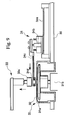
- FIG. 1 is a front view showing an embodiment of an apparatus for bonding disc substrates according to the present invention.
- FIG. 2 and FIG. 3 are graphs showing the wavelength and transmissivity of ultraviolet light.
- FIG. 4 is a graph showing the emission characteristic of a light emitting diode for ultraviolet light emission.
- FIG. 5 is a front view, partially cut away, showing an apparatus for bonding disc substrates according to another aspect.
- FIG. 6A and FIG. 6B are a plan view and a front view of a semiconductor light emitting unit.
- FIG. 7A and FIG. 7B are a plan view and a front view of another example of a semiconductor light emitting unit.
- FIG. 8 to FIG. 13 are front views to explain the operation of an apparatus for bonding disc substrates of another embodiment.
- FIG. 14A and FIG. 14B are a plan view and a sectional view of a tacking mechanism.
- FIG. 15 is a sectional view to explain the function of the tacking mechanism.
- FIG. 16 is a graph showing the thickness of an adhesive layer.
- FIG. 17A and FIG. 17B are plan views of examples of centering members.
- FIG. 18 is a sectional view showing another embodiment of an apparatus for bonding disc substrates of the present invention.
- FIG. 19 is an enlarged sectional view of a disc mounting stage.
- FIG. 20 is a plan view of an emission mechanism.
- FIG. 21 and FIG. 22 are sectional views showing the operation of a centering mechanism.
- FIG. 23 is a sectional view of the centering mechanism.
- FIG. 24A to FIG. 24D are sectional views to explain an embodiment of a bonding method of the present invention.
- FIG. 25 is a sectional view to explain another example of a curing mechanism.
- FIG. 1 to FIG. 3 illustrate embodiment 1 of the present invention.
- reference symbols 1 and 2 denote disc shaped substrates such as disc substrates formed from polycarbonate, and an adhesive layer 3 (uncured state) spread by high speed rotation is formed between the substrates 1 and 2 .
- no recording layer is formed on the substrate 1
- a recording layer including a reflective layer is formed only on the substrate 2 .
- recording layers may be formed on both the substrates 1 and 2 . In this case, a recording layer including a semi-reflective layer is formed on the substrate 1 , and a recording layer including a reflective layer is formed on the substrate 2 .
- the substrates 1 and 2 are mounted on a flat, disc-shaped pedestal 4 , and the pedestal 4 is connected to an elevator unit 6 via an ascending and descending shaft 5 .
- a locating pin 4 a is provided in the center of the pedestal 4 for locating the substrates 1 and 2 . When the substrates 1 and 2 are mounted, the locating pin 4 a is inserted into the center holes of the substrates 1 and 2 .
- a semiconductor light emitting unit 7 is placed above the uppermost substrate 1 coaxially.
- the semiconductor light emitting unit 7 has a slightly larger outside diameter than the substrate 1 .
- the semiconductor light emitting unit 7 has a large number of light emitting diodes 7 a as light emitting semiconductor elements, and a support 7 b for supporting the light emitting diodes 7 a.
- the large number of light emitting diodes 7 a is arranged over the whole of the underside of the support 7 b, and emission faces X of the large number of light emitting diodes 7 a are all on the same plane.
- the light emitting diodes 7 a may be arranged closely at random. However, it is preferable to arrange them in multiple concentric circles having the same center as the substrate 1 . A certain space may be made between adjacent light emitting diodes 7 a, or they may touch each other.
- the light emitting diodes 7 a are all connected in parallel, and a resistor is connected in series with each of the light emitting diodes 7 a for protection.
- surface mount type light emitting diodes and resistors may be surface mounted on a disc shaped printed substrate serving as the support 7 b or part of it. Hence it is possible to assemble them easily even if there are about 350 to 450 of each.
- each of the light emitting diodes is connected to the negative terminal of a DC power supply 8 , and the anode side thereof is connected to the positive terminal via a protective resistor 9 and a switching device 10 .
- the most simple switching device 10 opens and closes the circuit for a fixed period.
- the switching device 10 may be equipped with a simple sequencer or a CPU in order to turn a prescribed number of light emitting diodes 7 a on and off sequentially.
- each emission surface X of the light emitting diodes 7 a is positioned so as to not touch the top surface of the uppermost substrate 1 , and the spacing from the surface of the uppermost substrate 1 is as small as possible. This is because light diminishes in proportion to the inverse square of the distance.
- the spacing between the emission surface X and the surface of the uppermost substrate 1 is 10 mm or less, and more preferably 1 to 7 mm.
- FIG. 2 and FIG. 3 the horizontal axis represents light wavelength, and the vertical axis transmissivity.
- Curve A shows the transmissivity of a polycarbonate substrate
- curve B the transmissivity of adhesive before being irradiated by ultraviolet light
- curve C the transmissivity of adhesive after curing by irradiation by ultraviolet light.
- Polycarbonate material is used for current optical disc substrates, and the transmissivity of a substrate formed from polycarbonate material increases rapidly when the wavelength is longer than approximately 280 nm.
- ultraviolet light since ultraviolet light is radiated onto the adhesive 3 through the substrate 1 or 2 of the optical disc to cure it, ultraviolet light whose wavelength is shorter than 280 nm is difficult to use because the transmissivity is low, and hence ultraviolet light with a wavelength of 280 nm or greater, preferably 300 nm or greater, is used, whose transmissivity is high.
- FIG. 2 and FIG. 3 there is a wavelength region where the transmissivity of ultraviolet light through the adhesive is lower before irradiation than after being cured by irradiation.
- the wavelength region where the transmissivity before irradiation by ultraviolet light from the light emitting diodes is lower than after irradiation is approximately 280 nm to 450 nm, and in this region the transmissivity of the adhesive increases as the adhesive cures by light irradiation.
- wavelengths where the absorption rate of ultraviolet light is high are effective for accelerating curing.
- a wavelength region of 280 nm to 600 nm was selected.
- the results of radiation of light with a range of wavelengths in this wavelength region onto adhesive through a substrate made of polycarbonate confirmed that a photopolymerization reaction of the adhesive occurred when the light wavelength emitted by the light emitting diodes was between 280 nm and 450 nm.
- the photopolymerization reaction of the adhesive occurred successfully, and it was also confirmed that there was no detrimental effect on the substrates, the recording layers and the like.
- the wavelength region of 280 to 450 nm is almost the same as the wavelength region where the transmissivity of ultraviolet light before curing adhesive is lower than the transmissivity of ultraviolet light after curing it.
- FIG. 4 shows the characteristics of a commercial ultraviolet light emitting semiconductor element, wherein the horizontal axis represents wavelength, and the vertical axis relative emission intensity.
- the ultraviolet light emitting semiconductor element emits light within a narrow wavelength width, approximately 360 nm to 420 nm, and the peak is at approximately 380 nm.
- This ultraviolet light at a wavelength of approximately 380 nm is within the desirable wavelength range of 300 nm to 420 nm, so it is clear that this commercial ultraviolet light emitting semiconductor element is suitable as a source of ultraviolet light emission.
- a light source for emitting ultraviolet light it is desirable to use ultraviolet light emitting diodes that emit ultraviolet light with wavelengths as shown in FIG. 4. Almost all light emitted from ultraviolet light emitting diodes that emit ultraviolet light with wavelengths as shown in FIG. 4 can be used for curing the adhesive layer between substrates.
- the operation of the apparatus will be described. After the substrates 1 and 2 are joined together via the intermediate adhesive layer 3 , the adhesive is spread uniformly by high speed rotation using a typical spinner, which is not shown in the figure.
- the substrates 1 and 2 are mounted on a substrate pedestal 4 using a typical substrate transfer mechanism, which is not shown in the figure.
- the elevator unit 6 raises an elevator shaft 5 , and when the surface of the uppermost substrate comes within a distance of 1 mm to 10 mm, preferably 7 mm, of the emission surface X of the semiconductor light emitting unit 7 , the elevator unit 6 is stopped.
- the switching device 10 operates, current flows from a DC power supply 8 through a switching element, which is not shown in the figure, the protective resistor 9 , and all of the light emitting diodes 7 a of the semiconductor light emitting unit 7 .
- all of the light emitting diodes 7 a emit ultraviolet light mainly in a wavelength range of 280 to 450 nm.
- the ultraviolet light is radiated onto the adhesive layer 3 through the uppermost substrate 1 to cure the adhesive layer 3 . This may be semi-cured.
- the elevator unit 6 operates again, and lowers the elevator shaft 5 , and the substrates 1 and 2 on the substrate pedestal 4 are then removed by the typical substrate transfer mechanism.
- the light emitting diodes 7 a Although the light emitted by the light emitting diodes 7 a is not strong, the light emitting diodes 7 a generate smaller heat, and have less thermal effect on substrates than an ultraviolet light emitting lamp such as a typical xenon lamp. Accordingly, it is possible to reduce the distance between the emission surface X of the semiconductor light emitting unit 7 and the uppermost substrate 1 significantly as described above, compared with the case of using a lamp. Accordingly, it is possible for light from the light emitting diodes of the semiconductor light emitting unit 7 to cure adhesive in approximately the same time as in the case of the conventional lamp.
- the light emitting diodes are arranged closely, so that light from adjacent, surrounding light emitting diodes overlaps. Accordingly, even if one of the adjacent light emitting diodes is damaged, it is possible to reduce the effects to a minimum, and there is no physical, detrimental effect on curing the adhesive.
- the semiconductor light emitting unit 7 is larger than the outer circumferences of the substrates 1 and 2 by one light emitting diode, it is also possible to cure adhesive protruding between the outer edges of the substrates 1 and 2 .
- one or a plurality of light emitting diodes may be arranged at a location 1 mm to 10 mm away from the circumferences of the substrates 1 and 2 with identical spacing, and light from the light emitting diodes may be radiated onto the adhesive protruding between the substrates 1 and 2 effectively.
- a gas blowing nozzle for blowing an inexpensive, inert gas such as nitrogen gas may be provided in the location where the light emitting diodes, which are not shown in the figure, radiate, to surround the adhesive to be irradiated with nitrogen gas. In this case, curing of the adhesive in contact with the gas is promoted, and the curing time is reduced.
- the distance between the emission surface X of the semiconductor light emitting unit 7 and the substrates 1 and 2 is narrowed or widened by raising or lowering the pedestal 4 a.
- the arrangement may be such that the substrates 1 and 2 are mounted conventionally on a substrate pedestal on a turntable, which is not shown in the figure, and the turntable is rotated in the horizontal direction intermittently or continuously, so that the substrates 1 and 2 pass through a location a predetermined distance below the emission surface X of the semiconductor light emitting unit 7 .
- ultraviolet light from the semiconductor light emitting unit is radiated onto the adhesive while the substrates 1 and 2 are rotated by a spinner.
- a typical optical disc manufacturing process will be described.
- adhesive is typically applied to the internal circumference of one substrate in an annular pattern, then the other substrate is stacked on top of it. Afterwards, the stacked substrates are transferred to the spinner by a substrate transfer mechanism, which is not shown in the figure.
- a voltage may be applied between the substrates as required to deform the adhesive into a tapered form with the attractive force of the electric field.
- the outline of the spinner is as shown in FIG. 5, and has a turntable 11 , which supports a pair of substrates 10 stacked via intermediate adhesive and rotates them, a shaft 13 connecting the turntable 11 with a rotation drive unit 12 such as a motor, and a partition 14 surrounding the area around the substrates 10 on the turntable 11 , excluding the above.
- the spinner generally rotates the substrates 10 at a high rotation speed of 2000 to 6000 revolutions per minute for a predetermined time, thus removing excess adhesive from between the substrates by its centrifugal force, and forms an adhesive layer of a uniform desired thickness.
- the substrates 10 are removed from the spinner by a substrate transfer mechanism, which is not shown in the figure, transferred to an ultraviolet light irradiation mechanism, which is not shown in the figure, and irradiated by ultraviolet light to cure the adhesive between the substrates.
- the semiconductor light emitting unit 7 is placed above the substrates 10 .
- the semiconductor light emitting unit 7 may be the same as in the embodiment described previously.
- the excess adhesive between the substrates 10 is removed, and when the substrates 10 stop rotating, or at the point of time when the rotation speed slows before rotation stops, the semiconductor light emitting unit 7 is lowered by a vertical motion drive unit 15 and a vertical motion shaft mechanism 16 such that the emission surface X arrives at a location 1 to 10 mm, or preferably 1 to 5 mm, from the surface of the substrates 10 .
- the semiconductor light emitting unit 7 radiates ultraviolet light with a wavelength range of 280 to 450 nm onto the substrates 10 to cure the adhesive between the substrates.
- the substrates 10 in which the substrates 1 and 2 are bonded together completely in this manner, are removed from the spinner by the substrate transfer mechanism, which is not shown in the figure.
- Ultraviolet light may be radiated onto the substrates 10 while the substrates are stopped. However, in order to achieve uniformity of the amount of ultraviolet light irradiation, it is preferable to radiate ultraviolet light while rotating the substrates 10 at low speed. While the substrates 10 are rotating, ultraviolet light is radiated, and the substrates 10 may stop during irradiation.
- some ultraviolet light may leak from the semiconductor light emitting unit 7 and cure part of the adhesive attached to the inside of the partition 14 of the spinner.
- the semiconductor light emitting unit 7 is fixed above the spinner, and the substrates 10 may be lifted from the spinner to radiate ultraviolet light onto the substrates 10 from outside the spinner.
- an elevator unit which moves the shaft 13 and the turntable 11 up and down, is provided in addition to the rotation drive unit 12 .
- the elevator unit 15 and the elevator shaft 16 are not required to drive the semiconductor light emitting unit 7 up and down.
- the semiconductor light emitting unit 7 is fixed above the partition 14 of the spinner. In the spinner, when high speed rotation stops, the elevator unit raises the rotation drive unit 12 , the shaft 13 , the turntable 11 and the substrates 10 , and stops them in the vicinity of the semiconductor light emitting unit 7 .
- the semiconductor light emitting unit 7 then radiates ultraviolet light in the aforementioned region onto the substrates 10 to cure the adhesive between the substrates when the surface of the substrates 10 arrives at the location 1 to 7 mm from the emission surface X.
- the adhesive inside the partition 14 is not cured by ultraviolet light.
- the substrate transfer mechanism which is not shown in the figure, attracts and holds the surface of the substrates to remove them from the spinner, there is a possibility of detrimental effects occurring such as a slight shift of the substrates, distortion and the like.
- the substrates are removed from the spinner after the adhesive layer between them is cured, such detrimental effects do not occur.
- FIG. 6A shows an example of an arrangement of light emitting semiconductor elements 7 a, wherein the lines a, b, c to n are arranged in concentric circles in the disc shaped support 7 b.
- Line a represents the innermost circle
- line b represents the second circle from the inside
- line n represents the outermost circle.
- the support 7 b is a disc shaped, printed substrate.
- the concentric circular lines a, b, c to n the light emitting diodes on each of the lines a, b, c to n are all connected in parallel by a conductive pattern P.
- the innermost line a is connected to line b in series by connecting a light emitting diode a 1 to a light emitting diode b 1 of line b, which is the next line out, by a conductive pattern P 1 .
- Line b and line c which is the third line from the inside, are connected in series by connecting a light emitting diode b 1 and a light emitting diode c 1 of line c by a conductive pattern P 2 .
- Line c and the fourth line d are connected in series by connecting a light emitting diode c 1 and a light emitting diode d 1 of line d by a conductive pattern P 3 .
- the other adjacent lines are similarly connected in series by conductive patterns.
- T 1 and T 2 are input terminals, and when a predetermined voltage is applied to the input terminals T 1 and T 2 , the light emitting diodes of each of the lines a, b, c to n all emit at the same time
- switching elements 20 a, 20 b, to 20 n may be installed between the light emitting diodes a 1 and b 1 , between b 2 and c 2 , and so on to between n ⁇ 1 and n, respectively, such that they connect between them in series.
- a drive unit 21 may be installed at the back of the disc shaped, printed substrate 7 b to switch the switching elements 20 a, 20 b, to 20 n on and off sequentially.
- the switching element 20 a is installed between the light emitting diode a 1 and the light emitting diode b 1 , one end of the switching element 20 a is connected to the light emitting diode a 1 via a through hole BH formed on the printed substrate 7 b, and the other end of the switching element 20 a is connected to the light emitting diode b 1 via another through hole BH formed on the printed substrate 7 b.
- the switching element 20 b is provided between the light emitting diode b 2 and the light emitting diode c 2 , and one end of the switching element 20 b is connected to the light emitting diode a 2 via a through hole BH formed on the printed substrate 7 b, and the other end of the switching element 20 b is connected to the light emitting diode c 2 via another through hole BH formed on the printed substrate 7 b.
- Switching elements connected between the other predetermined light emitting diodes are located behind the switching elements 20 a and 20 b in FIG. 6B.
- the drive unit 21 switches the switching elements 20 a, 20 b etc. on for a certain time at fixed intervals. Accordingly, all of the light emitting diodes on line a emit first, and after a predetermined time, 20 ms for example, the switching element 20 a is turned on, so that all of the light emitting diodes on line b also emit. Similarly, by switching the switching elements on, lines a, b, c to n emit in sequence. When a predetermined on time has elapsed, the switches are turned off in sequence every 20 ms from the switching element 20 a, and the light emitting diodes on line n stop emitting last. If a fixed sequential delay time is determined in advance, and the on time is also predetermined in this manner, it is also possible to use a delay circuit comprising a capacitor and a resistor for example, instead of switching elements.
- the emission time of the light emitting diodes corresponding to the regions which are difficult to cure is made longer than that of the light emitting diodes corresponding to the regions which are easy cure, and it is also possible to cure uniformly in the shortest photo-irradiation time.
- lines a, b, c to n are connected in series via the switching elements 20 .
- Lines a, b, c to n may be connected in parallel via each of the switching elements 20 .
- a photo-irradiation mechanism in which lines a, b, c to n are connected in parallel via switching elements, and a spinner as shown in FIG. 5, may be combined, and also a sensor may be installed that can measure the thickness of the adhesive layer from the innermost circle to the adhesive on the outermost circle.
- the thickness of the adhesive layer is measured from the innermost circle to the outermost circle, the measured value is compared with the set value stored in the CPU, and by switching on the switching elements of a line corresponding to a region where the thickness has reached the set value, firstly the light emitting diodes on this line are turned on, then the switching element corresponding to a region where the thickness of the adhesive layer next reaches the set value is turned on.
- the switching element corresponding to a region where the thickness of the adhesive layer next reaches the set value is turned on.
- the arrangement may be such that lines of light emitting diodes connected in series, or connected in parallel, or a predetermined plurality of them connected in series and then connected in parallel, are arranged in a spiral pattern.
- the diameter of the innermost side of the spiral pattern arrangement is smaller than the inner diameter of the adhesive layer between substrates, and the diameter on the outermost side is larger than the outer diameter of the adhesive layer between the substrates.
- delay elements which generate a delay for a predetermined time, or switching elements
- the emission surface in order for the emission surface to be equal to or slightly larger than the surface of the adhesive layer to be cured, a large number of light emitting diodes is arranged in a concentric circular pattern or a spiral pattern.
- the light emitting diodes may be arranged at random and close to each other, in a hexagonal pattern such that the spacing between adjacent light emitting diodes is a fixed distance, in a concentric circular pattern, a spiral pattern or the like.
- the light emitting diodes may be arranged such that the emission surface is made to be a part of the surface of the adhesive layer to be cured.
- the support 7 b of the semiconductor light emitting unit 7 has a fan-shaped printed substrate 7 b.
- a plurality of light emitting diodes 7 a is arranged at high density on this printed substrate 7 b, and they are all connected in parallel by a conductive pattern (not shown in the figure) formed on the printed substrate 7 b. Accordingly, all of the light emitting diodes 7 a are turned on and off at the same time.
- Their emission surface X is at a predetermined distance of 10 mm or less from the surface of the substrate 10 .
- the semiconductor light emitting unit 7 and the substrate 10 are rotated at a certain rotation speed relative to each other.
- a rotation drive mechanism is required to rotate the substrate 10 .
- the support 7 b is fan shaped, the number of light emitting diodes 7 a arranged on the external outer arc is larger than that on the inner arc in proportion to the radius. Therefore, the irradiation time can be equal although the circumferential speeds are different between the inner arc and the outer arc.
- This semiconductor light emitting unit 7 can reduce the number of light emitting diodes required significantly compared with the aforementioned embodiment, and can reduce the cost. However, if light emitting diodes with the same characteristics are used, the time to cure the adhesive layer is longer.
- the light emitting diodes emit light continuously, but they may emit light in a pulse pattern, that is intermittently.
- a high peak current to flow into the light emitting diodes to generate ultraviolet light of high luminous intensity.
- a curing adhesive of higher quality may be expected.
- the width and peak value of the current pulse supplied to each of the light emitting diodes, or the width of the dead time between current pulses, as required it is possible to cure the adhesive more uniformly and with higher quality.
- Adhesive suitable for the present invention will be described.
- commercial ultraviolet light curing type adhesive usually contains photoinitiator which reduces the sensitivity to ultraviolet light so that curing does not start during handling.
- a light emitting diode has a lower luminous intensity of ultraviolet light than a flash lamp, it is preferable to increase the amount of photoinitiator which enhances the sensitivity to ultraviolet light.
- the photoinitiator added to the adhesive is increased to enhance the sensitivity to ultraviolet light, it is not possible to handle the adhesive in a conventional environment, and hence red light emitting diodes are used, preferably, for the environment lighting in this case.
- red light emitting diodes emit ultraviolet light with a wavelength of tens of nm centered at 645 nm, and do not contain wavelengths in a wavelength range of 300 to 420 nm, so that adhesive with high sensitivity can be used in an environment lit by red light emitting diodes similarly to the conventional method. Furthermore, since yellow light emitting diodes emitting a yellow light with a wavelength of around 590 nm, and green light emitting diodes emitting a green light with a wavelength of around 520 nm do not contain wavelengths in a wavelength range of 300 to 420 nm fundamentally, it is possible to use them for lighting.
- ultraviolet light emitting diodes in an apparatus for curing adhesive whose sensitivity to ultraviolet light is increased, and by using light emitting semiconductor elements that do not contain wavelengths in a wavelength range of 280 to 450 nm, such as red light emitting diodes, yellow light emitting diodes, or the like for the lighting of areas where the adhesive is handled, it is possible to reduce power usage costs significantly, it is very desirable environmentally, and the costs also can be reduced.
- the description in the above embodiment uses optical disc substrates for the substrates.
- the substrates may be other transparent sheet type materials, such as glass, lenses, and the like, whose light transmissivity is high, and it is possible to bond them by curing similarly to the above.
- a semiconductor light emitting unit comprises light emitting diodes.
- solid-state lasers such as semiconductor lasers, which generate visible light laser beams with similar wavelengths may also be used.
- solid-state lasers are arranged such that the light focus of the solid-state lasers is soft, and the spacing between the semiconductor light emitting unit and the irradiation surface is large, so that a uniform light is radiated onto the irradiation surface.
- an argon gas laser which generates a laser beam with a wavelength of primarily 488.5 nm
- a gas laser such as a helium/neon gas laser, which generates a laser beam with a wavelength of 632.8 nm
- a dye laser of an appropriate color, or the like as a light source.
- a part or the whole of the adhesive may be semi-cured or cured by radiating ultraviolet light with a peak wavelength in the range of 280 to 450 nm for tacking purposes.
- a semiconductor laser with a wavelength peak in a wavelength range of 280 to 450 nm for example a bluish purple laser, which generates a laser beam with a wavelength of 405 nm
- a gas laser such as a YAG laser doped with neodymium (Nd), which generates a laser beam with a wavelength whose third harmonic is 355 nm, an Ar laser (diatomic ion) with a wavelength of about 351 nm or 364 nm, or the like may be used. It is also possible to perform tacking efficiently by using a gas laser, and radiating a laser beam onto the adhesive in only a non-recording region on the internal circumference side of the optical disc substrates while rotating the optical substrates to semi-cure or cure them.
- a lamp such as a fluorescent lamp may be combined with a bandpass filter that blocks wavelengths of and around 405 nm.
- the bandpass filter irradiates onto the optical disc substrates, visible light of wavelengths longer than 405 nm, being the wavelength of light emitted by a bluish purple laser that records on the recording film of the optical disc, and neighboring wavelengths, and preferably only visible light of wavelengths 430 nm or greater. At least light equal to or shorter than the wavelengths of and around 405 nm are blocked, and are not radiated onto the optical disc substrates.
- a spinner 31 rotates two disc substrates 32 stacked via intermediate adhesive at high speed to spread the adhesive between the two disc substrates and remove excess adhesive.
- the spinner 31 has a disc pedestal 31 a, which receives the two disc substrates 32 from a transfer mechanism 33 and attracts and holds them, a rotation drive unit 31 b such as an electric motor for rotating the disc pedestal 31 at high speed, a cylindrical outer wall 31 c for preventing removed adhesive from splashing, and a center pin 31 d.
- the transfer mechanism 33 transfers the two disc substrates stacked via intermediate adhesive from another place to the disc pedestal 31 a, mounts them, and transfers the bonded disc substrates 32 to a different place.
- the transfer mechanism 33 has an attraction head section 33 a for attracting or releasing the disc substrates, a handling section 33 b for moving the attraction head section 33 a in the vertical direction and horizontal direction, and a drive section (omitted in the figure) for driving the handling section 33 b.
- the tacking mechanism 34 is an essential element in this embodiment.
- the tacking mechanism 34 has a horizontal direction drive unit 34 a, such as a cylinder fixed on a base 35 , a vertical direction drive unit 34 b, such as a cylinder installed on the horizontal direction drive unit 34 a, an arm section 34 c fixed on the moving part of the vertical direction drive unit 34 b, and a tacking emission mechanism 34 d fitted at the end of the arm section 34 c.
- FIG. 14A and FIG. 14B show an example of a tacking emission mechanism 34 d.
- This tacking emission mechanism 34 d has a support member A 3 , which is fixed at the end of the arm 34 c, and a plurality of light emitting diodes B 3 , which are arranged in an annular pattern on the support member A 3 , and that are connected electrically in series or in parallel.
- the light emitting diodes B 3 are mounted on a ring shaped printed circuit board C 3 on which conductive patterns connected in parallel or series are formed.
- An input cable D 3 is installed for supplying direct current to the light emitting diodes.
- the disc substrates 32 have center holes, and have an internal circumference region of a predetermined width centered on the center holes, widely known as a non-recording region (for example, L shown in FIG. 15), where no information is recorded. Information is stored in the area outside the non-recording region L, which is an information recording region to be recorded on later.
- the light emitting diodes B 3 arranged in an annular pattern are arranged on an imaginary circle facing the non-recording region of the disc substrates 32 .
- One layer of light emitting diodes B 3 is fitted in the figure. However, since light such as ultraviolet light may be radiated onto the adhesive in the non-recording region of the disc substrates 32 , two or more rows of light emitting diodes B 3 may be fitted.
- the transfer mechanism 33 attracts the disc substrates 32 stacked via intermediate adhesive applied in a doughnut shape, using the attraction head section 33 a to move the substrates 32 directly above the disc pedestal 31 a of the spinner 31 .
- the handling section 33 b is lowered, and the handling section 33 b stops immediately before the disc substrates 32 touch the disc pedestal 31 a.
- the attraction head section 33 a stops attraction, and the disc substrates 32 are mounted on the disc pedestal 31 a.
- the disc substrates 32 are centered by the centering member 31 d located in the center of the disc pedestal 31 a.
- the handling section 33 b of the transfer mechanism 33 starts to ascend, and at the same time the rotation drive unit 31 b rotates the disc pedestal 31 a at high speed while the disc substrates 32 are attracted to the disc pedestal 31 a of the spinner 31 . In this manner, the disc substrates 32 are rotated at high speed to spread adhesive between the disc substrates, and remove excess adhesive.
- the horizontal direction drive unit 34 a of the tacking mechanism 34 operates, and moves the vertical direction drive unit 34 b and the arm section 34 c fixed thereon in the direction of the arrow, that is to say towards the left in the figure, moves the tacking emission mechanism 34 d at the end to a predetermined location, and then the horizontal direction drive unit 34 a stops operation.
- the vertical direction drive unit 34 b starts to descend, moves the arm section 34 c down vertically as shown in FIG. 10, and stops at a location where it does not touch the disc substrates 32 , for example at a location 0.4 mm or more from the top surface of the disc substrates.
- the tacking emission mechanism 34 d starts emission after the adhesive layer is spread between the disc substrates by high speed rotation, and radiates ultraviolet light onto only an adhesive layer formed in the non-recording region of the disc substrates 32 to semi-cure or cure the adhesive layer.
- the disc substrates 32 are preferably rotated at high speed at this time, which enables the adhesive layer to be semi-cured or cured uniformly. Although it depends on how long is required for tacking, in the case where a longer time is required for tacking than the time of high speed rotation, an appropriate low speed rotation time may be provided after the high speed rotation finishes.
- the tacking emission mechanism 34 d stops emitting ultraviolet light, and the vertical direction drive unit 34 b raises the arm section 34 c vertically upwards slightly as shown in FIG. 11.
- the horizontal direction drive unit 34 a operates to move the arm section 34 c to the initial position in the direction of the arrow, that is towards the right in the figure, and stops.
- the transfer mechanism 33 attracts and holds the tacked disc substrates 32 by the attraction head section 33 a, and lifts it to transfer it to the next location, for example a location for curing by ultraviolet light irradiation, which is not shown in the figure, and cures the adhesive sufficiently. Afterwards the same operations are repeated.
- the tacking emission mechanism 34 d as shown in FIG. 15 starts emitting ultraviolet light when a predetermined time has elapsed after the spinner 31 starts rotating at high speed.
- the predetermined time cannot be set to an absolute value since it is affected by characteristics such as the viscosity of adhesive, temperature, humidity of the environment, and the like, but is determined by the conditions at the time using experimental data obtained and stored in advance in a CPU.
- the predetermined time can also be set according to the characteristics of the adhesive to be used, by maintaining the environment at a constant temperature, humidity and the like.
- light emitting diodes are used for the tacking light emitting mechanism 34 d of the tacking mechanism 34 .
- semiconductor lasers or gas lasers may be used.
- the arrangement may be such that one semiconductor laser, or a plurality of them arranged at equal spacing or in a zigzag, replaces the light emitting diodes.
- gas lasers since greater power can be obtained than from semiconductor lasers, using one gas laser, the gas laser may be arranged such that the laser beam is radiated onto the non-recording region of the disc substrates, and the disc substrates may be rotated.
- the disc substrates are not necessarily rotated, and it is also possible to rotate the tacking light emitting mechanism 34 d of the tacking mechanism 34 .
- the tacking power can be improved without using a laser beam by forming the disc pedestal 31 a from a transparent material such as glass, arranging another tacking light emitting mechanism 34 d below the disc pedestal 31 a, and radiating ultraviolet light onto the adhesive layer from both sides of the disc substrates 32 , which enables the tacking to be performed in a shorter time.
- the adhesive layer of the disc substrates on the disc pedestal of the spinner is tacked.
- the diameter of the centering member must be sufficiently smaller than the center hole of the disc substrates 32 .
- the construction is such that a centering mechanism is provided at a location where the substrates are mounted temporarily, and the diameter of the centering member 31 d of a pedestal, which is not shown in the figure, can be expanded and contracted.
- the centering member 31 d has a structure consisting of three 120° segments around its center, and it expands and contracts the fan shaped centering pieces 1 d 1 , 1 d 2 and 1 d 3 using a drive unit, which is not shown in the figure.
- a normal state as shown in FIG. 17A, the diameter of the centering pieces 1 d 1 , 1 d 2 and 1 d 3 is contracted, so the outline of the centering member 31 d is small.
- the disc substrates 32 are mounted on the pedestal, which is not shown in the figure, while the diameter is contracted, so that the centering member 31 d is inserted into the center hole H 3 of the disc substrates 32 .
- the tacking light emitting mechanism 34 d of the tacking mechanism is arranged as shown in FIG. 15, and ultraviolet light is radiated onto the adhesive layer in the non-recording region for tacking.
- the centering member 31 d is not limited to the structures shown in FIG. 17A and FIG. 17B provided that it expands and contracts its diameter. The embodiments of FIG. 17A and FIG.
- FIG. 17B show constructions in which the diameter of the centering member 31 d of the pedestal, which is not shown in the figure, being a temporary mounting location, can be expanded and contracted.
- the construction may be such that the diameter of the centering member of the spinner can be expanded and contracted.
- the adhesive layer in the non-recording region on the inner side of the disc substrates is semi-cured or cured, it has no effect on curing the adhesive layer later, compared with the case where the adhesive layer in the non-recording region on the outer side is semi-cured or cured.
- the disc substrates 32 and the tacking light emitting mechanism 34 d do not always rotate relative to each other, and the tacking light emitting mechanism 34 d may touch the surface of the non-recording region of the disc substrates 32 .
- the tacking light emitting mechanism 34 d radiating ultraviolet light onto the whole surface or part of the non-recording region and the information recording region of the disc substrates 32 to semi-cure or cure the adhesive layer between the disc substrates corresponding to the non-recording region and the information recording region of the disc substrates.
- Each of the disc substrates may consist of two disc substrates bonded together.
- One disc substrate may be a thin film, which will become a cover layer of a next generation DVD.
- an attraction head is described. However, other types such as those that hold mechanically may also be used instead of the attraction type.
- FIG. 18 shows a disc mounting stage used in a third embodiment of a disc substrate bonding apparatus.
- the disc mounting stage basically comprises a mounting stage 43 for supporting disc substrates 41 a and 41 b stacked via intermediate adhesive, and a centering mechanism 44 , which is inserted into the center holes of the disc substrates 41 a and 41 b, and an emission mechanism 45 , which encircles it and is fitted on the mounting stage 43 .
- the emission mechanism 45 comprises a plurality of light emitting diodes 46 arranged in an annular pattern, and the light emitting diodes 46 are mounted on an annular shaped printed circuit board 47 on which a conductive pattern is formed.
- the light emitting diodes 46 arranged in an annular pattern are arranged inside the mounting stage 43 facing toward a non-recording region (for example, L as shown in FIG. 19) of a predetermined width centered on the center holes of the disc substrates 41 and 41 b.
- the light wavelength region in which the light emitting diodes emit light is preferably from 280 nm to 450 nm, considering the wavelength characteristics of the disc substrates, the wavelength region where the photopolymerization reaction of adhesive occurs, and the like.
- a thin heat sink made of aluminum which is not shown in the figure, is provided at the back of the printed circuit board 47 where the light emitting diodes 46 are mounted. Furthermore, the printed circuit board 47 where the light emitting diodes 46 are mounted is held in an annular shaped support member 48 .
- a cooling medium distribution path 410 through which air is passed is provided under the heat sink. Cooling air which is supplied from a supply port 411 a, cools the heat sink while passing through the annular shaped cooling medium distribution path 410 , and is then exhausted from an exhaust vent 411 b.
- Heat generated by the light emitting diodes 46 is dissipated by the aluminum heat sink. Furthermore, since the surface of the heat sink is cooled, the cooling efficiency is high, so that it is possible to prevent the disc substrates from being affected by heat conduction and the light emitting diodes 46 from being damaged by the heat generated.
- the emission mechanism 45 where the light emitting diodes 46 are mounted on the support member 48 can be handled as a single component. Accordingly, in the case where the light emitting diodes 46 are damaged, the whole emission mechanism can be changed, which makes maintenance easy.
- Numeral 49 shown in FIG. 18 denotes a cylinder having a cylinder rod 49 a, operating as an up-and-down drive unit.
- the centering mechanism 44 comprises a shaft 412 , which is moved up and down, and an elastic body 413 .
- the shaft 412 is column shaped, and has an umbrella section 412 a on the top, which expands radially from the shaft 412 like an umbrella.
- the bottom of the shaft 412 is connected to the cylinder rod 49 a of the cylinder 49 , being a drive mechanism that moves the shaft 412 up and down.
- the elastic body 413 is made of a resin having an appropriate elasticity and hardness, such as silicon rubber for example. As shown in FIG. 18, the elastic body 413 is installed around the shaft 412 , and the top of the elastic body 413 is pressed down by the bottom of the umbrella section 412 a. The elastic body 413 has an appropriate thickness, and there is a gap 415 between the elastic body 413 and the side face of the shaft 412 .
- the silicon rubber elastic body 413 inserted into the center holes of the two disc substrates 41 a and 41 b stacked via intermediate adhesive 42 , expands radially, thus pressing the internal circumference side faces 416 a and 416 b of the disc substrates 41 a and 41 b to correct any shift.
- the silicon rubber elastic body 413 When the silicon rubber elastic body 413 is expanded in the radial direction, it is preferable that the arc of the side face of the elastic body 413 is large, and the closer it is to flat, the better. In the case of a small arc, since optimal pressure cannot be applied to the internal circumference side faces 416 a and 416 b of the center holes of the stacked disc substrates 41 a and 41 b, there is a possibility in that force applied to the stacked disc substrates pulls them apart. Therefore, the elastic body 413 needs to be a certain height, so the elastic body 413 of the present embodiment has a height of around 10 mm from the surface of the disc substrate 41 a mounted on the mounting stage 43 .
- FIG. 24A An example of a method for bonding disc substrates will be described using FIG. 24A to FIG. 24D.
- the two disc substrates 41 a and 41 b stacked via intermediate adhesive 42 are mounted on the mounting stage 17 of the spinner for high speed rotation to spread the adhesive 42 between the disc substrates uniformly, and remove excess adhesive.
- the disc substrates are mounted on the disc mounting stage 43 of the present invention by a transfer mechanism, which is not shown in the figure, and the center holes of the disc substrates are inserted into a centering mechanism 44 .
- the disc mounting stage 43 is located between the spinner of a bonding apparatus and an ultraviolet light irradiation apparatus.
- a cylinder rod 49 a of a cylinder 49 operates to lower a shaft 412 , so that the elastic body 413 is pressed down from the top, and expands in the radial direction of the disc substrates.
- the shift between the disc substrates is corrected for accurate centering with no detrimental effect on the tilt.
- the centered and tacked disc substrates are transferred to a mounting stage 418 of an ultraviolet light curing apparatus at another location, and irradiated by ultraviolet light from an ultraviolet light radiating lamp 419 , so that the adhesive 42 of the whole area between the substrates is completely cured.
- the stacked disc substrates are centered accurately on the disc mounting stage 43 of the present invention.
- the centering mechanism 44 is not limited to this embodiment.
- an emission mechanism 45 is described in which light emitting diodes are arranged in a location corresponding to the internal circumference of the disc substrates.
- the emission mechanism 45 may have light emitting diodes arranged over a surface area corresponding to the whole surface of the disc substrates, light emitting diodes arranged in an annular pattern in the center, light emitting diodes arranged radially in one or more rows at 90° spacing or at 120° spacing, or the like.
- the emission mechanism 45 is installed in the disc mounting stage 43 .
- the disc mounting stage 43 may move up and down as required.
- the emission mechanism 45 is not limited to light emitting diodes.
- Semiconductor lasers, or an ultraviolet light radiating lamp such as a xenon lamp, a metal halide lamp, or the like may be used.
- a plurality of semiconductor lasers arranged at equal spacing may be used instead of light emitting diodes.
- an ultraviolet light radiating lamp a small sized, annular shaped one may be utilized.
- FIG. 25 an embodiment is shown in which ultraviolet light is radiated onto the whole surface of adhesive spread between disc substrates to cure it at the same time as centering is performed.
- one or more annular shaped ultraviolet light radiating lamps 420 which are smaller than conventional ones, are provided inside a disc mounting stage 43 , and the whole surface of adhesive 42 spread between the disc substrates is cured by irradiation from the ultraviolet light radiating lamps 420 .
- the ultraviolet light radiating lamps 420 are inside the disc mounting stage 43 , whose inner diameter is almost the same as the outer diameter of the disc substrates 41 a and 41 b, the surface of the disc mounting stage 43 facing the disc substrates is open, or covered by heat-resistant glass, and its other surface is in a condition close to a mirror finished surface. As a result, ultraviolet light is radiated onto the disc substrates efficiently.
- the arrangement may be such that a plurality of ultraviolet light irradiation mechanisms with a structure as shown in FIG. 25 is installed in a rotating transfer mechanism such as a turntable, so that the whole surface of the adhesive can be cured completely during a process of transferring to a predetermined location.
- the arrangement may also be such that a plurality of disc mounting stages is installed in which light emitting diodes are arranged on a surface area corresponding to the whole surface of the disc substrates, so that the whole surface of the adhesive can be cured completely.
- disc substrates to be bonded the effects of the present invention can be obtained even in a case where disc substrates have different thicknesses, for example, one disc substrate is a thin film.
Abstract
An apparatus for bonding disc substrates is provided with a spinner which spreads adhesive placed between a first substrate and second substrate, and a curing device which radiates ultraviolet light onto the adhesive through the substrate to cure it. The curing device includes; a support mechanism which supports the first substrate and second substrate after the adhesive is spread by the spinner, a semiconductor light emitting apparatus having a plurality of light emitting semiconductor elements arranged facing a region where the adhesive is cured, and a positioning mechanism which positions the semiconductor light emitting apparatus such that the light emitting semiconductor elements are a predetermined distance away from the adhesive. The adhesive is cured or semi-cured by ultraviolet light emitted from the plurality of light emitting semiconductor elements.
Description
- 1. Field of the Invention
- The present invention relates to a method and an apparatus for curing adhesive, which are suitable for curing adhesive applied between substrates such as those for optical discs and the like, and an apparatus for bonding disc substrates.
- 2. Description of Related Art
- In general, an optical disc such as a DVD or the like has a structure in which two transparent substrates are bonded together by adhesive. Some of them have a recording layer including a reflective layer or a semi-reflective layer formed on only one of the substrates, and some have recording layers formed on both substrates. In the case where a recording layer is formed on only one substrate, the thickness of the two substrates may be the same, or the substrate on which no recording layer is formed may be formed with a thin, transparent sheet. Some have a structure in which two pairs of substrates are bonded together in a laminate of four substrates. Furthermore, in some cases a plurality of sheets of transparent glass or lenses are bonded to each other via intermediate adhesive.
- When manufacturing such an optical disc, after two substrates have been stacked via intermediate adhesive, the adhesive is spread evenly over the substrates by high speed rotation, and excess adhesive is removed. Afterwards, ultraviolet light is normally radiated onto one or both sides of the substrate to cure the adhesive quickly. Regarding the ultraviolet light radiation, ultraviolet light is radiated continuously for a prescribed time using a UV lamp, or pulsed ultraviolet light is radiated using a xenon lamp.
- However, the method of curing using these lamps has the following problems.
- (1) Since ultraviolet light emitting lamps have low luminous efficiency, and generate significant heat, there is a possibility of the heat distorting the substrates. Furthermore, since a suitable heat dissipation mechanism is required, the size of the apparatus increases, and the cost is high.
- (2) Since ultraviolet light emitting lamps are expensive, and their lifetime is short, the running costs are high. Those with a short lifetime must be changed after several tens of hours, which has a detrimental effect on productivity.
- (3) In the case of radiating pulsed ultraviolet light, there is an advantage in regard to heat compared with continuous radiation. However, the shock during irradiation is great, so there is a possibility in that vibration during that time may damage the objects to be bonded, such as glass, or have a detrimental effect on adhesiveness. Furthermore, the sound caused by the shocks during irradiation increases the ambient noise level and is not desirable environmentally. In order to solve these problems, conventionally a damping mechanism or a noise control mechanism has been installed. However, this invites a further increase in the size of the apparatus and increases costs.
- (4) In the case of lamps, power loss is considerable, so there are disadvantages from both environmental and cost standpoints.
- Examples of a conventional DVD manufacturing apparatus and its manufacturing method are described in Japanese Unexamined Patent Application, First Publication No. 2002-245692 (
pages 6 to 8, FIG. 1), and Japanese Unexamined Patent Application, First Publication No. 09-231625 (pages 3 to 5, FIG. 1). - In the apparatus described in the references above, adhesive is placed between two disc substrates, the adhesive is spread by a spinner, and the disc substrates are transferred to a pedestal by a transfer mechanism. During this transfer process the adhesive is not cured, and hence there is a possibility in that disc substrates newly bonded together may move. If this happens, they will cure in this state, which causes a drop in quality. Furthermore, there is also a concern that the area around the center hole of the stacked disc substrates may be pulled apart and contaminated by bubbles when the center holes of the disc substrates are mounted on the center pin of a mounting stage in an ultraviolet light irradiating apparatus. Consequently, the uniformity in the tilt and thickness of the completed optical disc is affected, and there is a problem that the quality of the optical disc and the production efficiency deteriorate.
- Especially, the uniformity of the tilt and thickness is a major problem for Blu-Ray Disc, which have a very thin, 0.1 mm thick light transmission layer formed from an adhesive layer and a protective sheet, or large capacity optical discs called AOD (Advanced Optical Disc) in which two disc substrates with a thickness of 0.6 mm, which is the same as a DVD, are bonded together, and which require a sufficiently tight tolerance on the thickness of the adhesive film.
- In order to solve the above problems, Japanese Unexamined Patent Application, First Publication No. 10-97740 discloses a technique in which disc substrates are transferred after high speed rotation, and the stack of disc substrates is centered, and then cured from above by an emission mechanism moved from a different location, for tacking.
- However, this method requires a process in which disc substrates are mounted on a mounting stage for centering, and then a retracted emission mechanism is moved over the disc substrates. Accordingly, operating the apparatus at high speed is difficult, and requires appropriate mechanisms. Furthermore, the inside diameters of the center holes of the disc substrates vary, and hence there is a concern that the inside diameters do not match when the two disc substrates are laminated. Conventionally, when the diameter of a metal member formed from a plurality of blocks is expanded, and applies a pressure to the internal circumferences of the center holes of the disc substrates to center them, a high load is applied to disc substrates with a small inside diameter, which affects the tilt of the disc substrates. Therefore, fine pressure adjustment is difficult.
- A method of curing adhesive between substrates according to the present invention comprises a step for emitting ultraviolet light using a light emitting semiconductor element or a gas laser, and a step for radiating the ultraviolet light onto adhesive spread between first and second substrates through at least one of the first substrate and the second substrate to cure or semi-cure the adhesive.
- According to this method, since a light emitting semiconductor element or a gas laser is used, heat generation can be lower than from a conventional lamp, and hence the influence of heat on the substrates can be reduced. Since the lifetime is significantly longer than a lamp, running costs can be reduced. Furthermore, the electrical energy used for the emission is small, so that influences on the environment can be reduced.
- The ultraviolet light may have wavelengths in a range where a transmissivity of the adhesive before curing is lower than the transmissivity of the adhesive after curing. In this case, since the transmissivity of the ultraviolet light improves as the adhesive cures, it is possible to cure the adhesive more effectively.
- The wavelength of the ultraviolet light may be mainly in a range of 280 to 450 nm. In this case, the influence of heat on the substrates can be reduced, and the transmissivity of the ultraviolet light improves as the adhesive cures. Therefore, it is possible to cure the adhesive more effectively.
- A distance between an emission surface of ultraviolet light from the light emitting semiconductor element or the gas laser and an irradiated surface of the substrate may be 10 mm or less. In this case, the influence of heat on the optical disc can be reduced, and the adhesive can be cured more efficiently. More preferably, it is 7 mm or less.
- During irradiation by the ultraviolet light, the ultraviolet light and the adhesive may be moved relative to each other. In this case, it is possible to cure the adhesive more uniformly.
- A recording layer may be formed on at least one of the first substrate and second substrate, and the ultraviolet light that the light emitting semiconductor element or the gas laser emits may be radiated from the circumference side of the first or second substrates onto the adhesive. In this case, it is possible to cure the adhesive to a more desirable state, and to do it uniformly.
- After the adhesive is semi-cured or cured, the substrate may be transferred to a next process, and the adhesive may be cured by irradiation by ultraviolet light. In this case, it is possible to cure the adhesive to a more desirable state. After the adhesive is semi-cured, since the amount of ultraviolet light required to cure the adhesive is small, it is possible to cure the adhesive sufficiently by suitable weak ultraviolet light.
- After spreading the adhesive applied between the first and second substrates by high speed rotation, ultraviolet light may be radiated onto it progressively from the internal circumference of the first substrate and the second substrate to the external circumference, while the substrate is rotated slowly, or while the substrate is stopped. In this case, it is possible to cure the adhesive more efficiently, and hence enable quality to be improved.
- Either one of the first substrate and the second substrate or both may be polycarbonate. In this case, ultraviolet light of a longer wavelength than the wavelength at which the transmissivity of light saturates for polycarbonate may be radiated. In this case, it is possible to cure the adhesive more efficiently, and hence enable the influence of heat on the substrate to be reduced.
- The ultraviolet light may be radiated onto the adhesive protruding from between the first substrate and the second substrate in an atmosphere where an oxygen concentration is lower than in air. In this case, it is possible to cure the adhesive protruding from between the substrates more efficiently and more effectively.
- A thickness of an adhesive layer between the first and second substrates may be detected, and the ultraviolet light radiated when the thickness reduces to a preset thickness with the high speed rotation. In this case, it is possible to cure the adhesive more efficiently.
- The thickness of the adhesive layer between the first and second substrates may be detected, and the ultraviolet light radiated progressively from an area whose thickness is reduced to a preset thickness with the high speed rotation.
- A curing apparatus of the present invention radiates ultraviolet light onto an adhesive spread between first and second substrates through at least one of the first substrate and second substrate for curing. This apparatus comprises a support mechanism which supports the first substrate and second substrate, a semiconductor light emitting apparatus having a plurality of light emitting semiconductor elements arranged facing a region where the adhesive is cured, and a positioning mechanism which positions the semiconductor light emitting apparatus such that the light emitting semiconductor elements are a predetermined distance away from the adhesive, and the adhesive is cured or semi-cured by ultraviolet light emitted from the plurality of light emitting semiconductor elements.
- According to this apparatus, heat generation is far less than from a conventional lamp, so the influence of heat on the substrates can be reduced. Furthermore, since the lifetime is significantly longer than an ultraviolet light lamp, running costs are reduced, and the electrical energy used for emission is low.
- The plurality of light emitting semiconductor elements may be arranged along any of a helical, concentric circular, or polygonal pattern. Furthermore, the plurality of light emitting semiconductor elements may be arranged at random.
- The plurality of light emitting semiconductor elements may be arranged in a helical pattern, and the light emitting semiconductor elements may irradiate ultraviolet light from the inside to the outside progressively with time. In this case, it is possible to cure the adhesive more effectively. Furthermore, it is possible to release the stress occurring in the adhesive layer by curing from the internal circumference to the external circumference, and hence the quality of the bonded substrates is improved.
- The plurality of light emitting semiconductor elements may be arranged in a concentric circular pattern, and the light emitting semiconductor elements in the concentric circular pattern, which are adjacent in the radial direction, may radiate ultraviolet light onto the adhesive from the inside toward the outside progressively with time.
- The light emitting semiconductor elements may be connected in parallel. Alternatively, a predetermined number of them may be connected in series, and then those groups of series connections may be connected in parallel. In this case, it is possible to use a low voltage power supply, and hence the reliability is also improved.
- The time duration may be almost the same as the curing time of the adhesive, or it may be longer.
- The semiconductor light emitting devices are preferably within 10 mm from the adhesive, and more preferably within 7 mm.
- The light emitting semiconductor elements of the curing apparatus may be arranged in one row or a plurality of rows so as to extend from the internal circumference to the external circumference of the substrate, and at least one of the support mechanism and the positioning mechanism may rotate the semiconductor light emitting apparatus and the first and second substrates relative to each other.
- The curing apparatus may be provided with a gas blowing mechanism for blowing an inert gas such as nitrogen gas or the like onto the surface of the adhesive where ultraviolet light is radiated.
- The light emitting semiconductor elements may be fixed onto a printed substrate, and connected to a conductive pattern formed on the printed substrate.
- An apparatus for bonding disc substrates of the present invention is provided with a spinner which spreads adhesive placed between a first substrate and second substrate, and a curing device which radiates ultraviolet light onto the adhesive through the substrate to cure it, wherein the curing device comprises; a support mechanism which supports the first substrate and second substrate after the adhesive is spread by the spinner, a semiconductor light emitting apparatus having a plurality of light emitting semiconductor elements arranged facing a region where the adhesive is cured, and a positioning mechanism which positions the semiconductor light emitting apparatus such that the light emitting semiconductor elements are a predetermined distance away from the adhesive, and the adhesive is cured or semi-cured by ultraviolet light emitted from the plurality of light emitting semiconductor elements.
- After the adhesive between the first substrate and second substrate is spread by high speed rotation of the spinner turntable, the ultraviolet light may be radiated onto the adhesive from above the turntable.
- When the ultraviolet light is radiated onto the adhesive, the turntable may be rotated.
- When the ultraviolet light is radiated onto the adhesive, the turntable may be located above a partition of the spinner.
- The curing device may further comprise an emitting device which radiates light onto the adhesive spread by the spinner to semi-cure or cure it for tacking the first substrate and second substrate, and a disc transfer mechanism which transfers the tacked first substrate and second substrate to the curing device.
- Tacking may be performed while the spinner is rotating. Tacking may be performed by semi-curing or curing the adhesive in a non-recording region where no recording layer is formed in the internal circumference of the optical disc substrate.
- An apparatus for bonding disc substrates of another aspect of the present invention comprises: a spinner that rotates the disc substrates stacked via an adhesive at high speed to spread the adhesive between the disc substrates; a tacking mechanism that radiates light through the disc substrates and starts to cure the adhesive spread between the disc substrates to tack the disc substrates together; a transfer mechanism which moves the tacked disc substrates to another location; and a curing device which cures the adhesive. This apparatus enables high quality discs to be obtained.
- The tacking mechanism may radiate light onto the disc substrates mounted on a disc pedestal of the spinner, for tacking.
- While the disc substrates are rotating at high speed in the spinner, the tacking mechanism may radiate light onto the adhesive in the non-recording region, which is a region on the disc substrates where no information is recorded, to stabilize an internal circumference of the adhesive layer.
- Another aspect of an apparatus for bonding disc substrates comprises: a spinner which rotates the disc substrates stacked via intermediate adhesive at high speed to spread the adhesive between the disc substrates; a transfer mechanism which transfers the bonded disc substrates to a centering location; a centering mechanism, which is positioned at the centering location and has a centering member that is inserted into a center hole of the bonded disc substrates to align the internal circumferences thereof; a tacking mechanism for tacking the disc substrates by radiating light through the centered disc substrates to start curing the adhesive layer between the disc substrates; a transfer mechanism which transfers the tacked disc substrates to a curing location; and a curing device, which is positioned at the curing location and cures the adhesive layer between the disc substrates.
- The tacking mechanism may semi-cure or cure the adhesive in a non-recording region, which is a region on the disc substrates where no information is recorded.
- The tacking mechanism may semi-cure or cure the adhesive in an information recording region of the optical disc substrates.
- The tacking mechanism may emit the light while it is rotated relative to the disc substrates.
- The tacking mechanism may be provided with light emitting diodes, a semiconductor laser, or a gas laser, which generates the light.
- The tacking mechanism may have a tacking emission mechanism which generates light to start curing the adhesive; an arm member at the end of which the tacking emission mechanism is installed; a vertical direction drive unit which supports this arm member and moves it up and down; and a horizontal direction drive mechanism that can support this vertical direction drive mechanism and move it in the horizontal direction.
- The tacking mechanism may radiate light onto the disc substrates mounted on the centering mechanism, for tacking.
- An apparatus for bonding disc substrates according to another aspect of the present invention comprises: a spinner which rotates a first and second disc substrate stacked via an adhesive at a high speed to spread the adhesive between the disc substrates; a disc mounting stage which is provided with a centering mechanism that is inserted into a center hole of the disc substrates for which the adhesive has been spread, to align the internal circumferences of the first and second disc substrates; and a disc substrate transfer mechanism which transfers the disc substrates from the spinner to the disc mounting stage, and the disc mounting stage is provided with an emission mechanism which radiates light onto the disc substrates whose internal circumferences are aligned to start curing the adhesive layer between the disc substrates.
- Using this apparatus, by providing a disc mounting stage, which has both a centering mechanism and an adhesive curing mechanism, at a separate location from the spinner, it is possible to realize accurate centering after a uniform adhesive layer is created by the spinner rotating at high speed, and to improve the production efficiency, thus enabling high quality optical discs to be obtained. Moreover, it is possible to start curing the adhesive almost at the same time as the accurate centering, so that it is possible to improve the quality and efficiency of producing the optical disc substrates.
- The emission mechanism may semi-cure or cure the adhesive on the whole surface or a partial region of the disc substrates. In this case, it is possible to bond or tack the disc substrates efficiently.
- The emission mechanism may semi-cure or cure the adhesive in a non-recording region of the disc substrates. By curing the adhesive in the non-recording region in the internal circumference of the disc substrates, it is possible to maintain the partially tacked and centered state. Furthermore, it is possible to adjust the spread of the adhesive in the internal circumference of the disc substrates, thus preventing adhesive from protruding from the internal circumference of the center hole of the disc substrates.
- The emission mechanism may have a plurality of light emitting diodes that generates the light. In this case, it is possible to miniaturize the emission mechanism, and reduce power consumption. Furthermore, the lifetime of the emission mechanism is long, and reliability is improved.
- The emission mechanism may have an annular ultraviolet light radiating lamp surrounding the centering mechanism. In this case, it is possible to complete the adhesive curing during centering, and a high quality optical disc can be obtained, and at the same time the production efficiency can be improved.
- The disc mounting stage may have a cooling medium distribution path for cooling the emission mechanism. In this case, it is possible to prevent the conduction of heat generated by the emission mechanism from affecting the disc substrates. Furthermore, it is possible to prevent the light emitting elements from being damaged.
- The centering mechanism may have a shaft which moves up and down inside the center hole of the disc substrates, a drive mechanism which is connected to the shaft, and an elastic body surrounding the shaft, which is put under pressure from above when the drive mechanism lowers the shaft, and expands in a radial direction of the disc substrates, and when the elastic body expands, the elastic force presses against the internal circumferences of the center holes of the first and second disc substrates. In this case, it is possible to apply optimal pressure to the internal circumferences of the center holes of both the first and second disc substrates for accurate centering.
- FIG. 1 is a front view showing an embodiment of an apparatus for bonding disc substrates according to the present invention.
- FIG. 2 and FIG. 3 are graphs showing the wavelength and transmissivity of ultraviolet light.
- FIG. 4 is a graph showing the emission characteristic of a light emitting diode for ultraviolet light emission.
- FIG. 5 is a front view, partially cut away, showing an apparatus for bonding disc substrates according to another aspect.
- FIG. 6A and FIG. 6B are a plan view and a front view of a semiconductor light emitting unit.
- FIG. 7A and FIG. 7B are a plan view and a front view of another example of a semiconductor light emitting unit.
- FIG. 8 to FIG. 13 are front views to explain the operation of an apparatus for bonding disc substrates of another embodiment.
- FIG. 14A and FIG. 14B are a plan view and a sectional view of a tacking mechanism.
- FIG. 15 is a sectional view to explain the function of the tacking mechanism.
- FIG. 16 is a graph showing the thickness of an adhesive layer.
- FIG. 17A and FIG. 17B are plan views of examples of centering members.
- FIG. 18 is a sectional view showing another embodiment of an apparatus for bonding disc substrates of the present invention.
- FIG. 19 is an enlarged sectional view of a disc mounting stage.
- FIG. 20 is a plan view of an emission mechanism.
- FIG. 21 and FIG. 22 are sectional views showing the operation of a centering mechanism.
- FIG. 23 is a sectional view of the centering mechanism.
- FIG. 24A to FIG. 24D are sectional views to explain an embodiment of a bonding method of the present invention.
- FIG. 25 is a sectional view to explain another example of a curing mechanism.
- Hereunder is a description of a plurality of embodiments of the present invention. However, the present invention is not limited to these embodiments and the structures of parts of the embodiments may be replaced with other known structures, and also the structures of the embodiments may be interchanged. Furthermore, the following embodiments use the present invention for bonding disc substrates. However, the present invention is not limited to this, and it can be used for any other application provided the application is to bond a pair of substrates with adhesive.
- [Embodiment 1]
- FIG. 1 to FIG. 3 illustrate embodiment 1 of the present invention. In FIG. 1,
reference symbols 1 and 2 denote disc shaped substrates such as disc substrates formed from polycarbonate, and an adhesive layer 3 (uncured state) spread by high speed rotation is formed between thesubstrates 1 and 2. In this example, no recording layer is formed on the substrate 1, and a recording layer including a reflective layer is formed only on thesubstrate 2. However, recording layers may be formed on both thesubstrates 1 and 2. In this case, a recording layer including a semi-reflective layer is formed on the substrate 1, and a recording layer including a reflective layer is formed on thesubstrate 2. - The
substrates 1 and 2 are mounted on a flat, disc-shapedpedestal 4, and thepedestal 4 is connected to anelevator unit 6 via an ascending and descendingshaft 5. A locatingpin 4 a is provided in the center of thepedestal 4 for locating thesubstrates 1 and 2. When thesubstrates 1 and 2 are mounted, the locatingpin 4 a is inserted into the center holes of thesubstrates 1 and 2. - A semiconductor
light emitting unit 7 is placed above the uppermost substrate 1 coaxially. The semiconductorlight emitting unit 7 has a slightly larger outside diameter than the substrate 1. The semiconductorlight emitting unit 7 has a large number oflight emitting diodes 7 a as light emitting semiconductor elements, and asupport 7 b for supporting thelight emitting diodes 7 a. The large number oflight emitting diodes 7 a is arranged over the whole of the underside of thesupport 7 b, and emission faces X of the large number oflight emitting diodes 7 a are all on the same plane. - The
light emitting diodes 7 a may be arranged closely at random. However, it is preferable to arrange them in multiple concentric circles having the same center as the substrate 1. A certain space may be made between adjacentlight emitting diodes 7 a, or they may touch each other. Thelight emitting diodes 7 a are all connected in parallel, and a resistor is connected in series with each of thelight emitting diodes 7 a for protection. During physical assembly, surface mount type light emitting diodes and resistors may be surface mounted on a disc shaped printed substrate serving as thesupport 7 b or part of it. Hence it is possible to assemble them easily even if there are about 350 to 450 of each. - One reason why the
light emitting diodes 7 a are connected in parallel rather than in series is that failure of alight emitting diode 7 a may be of a short circuit type or an open circuit type, and if connected in series, emission of the semiconductorlight emitting unit 7 may be disrupted if the failure is an open circuit type. An other reason is that since the voltage drop of each light emitting diode is several volts, if 350 to 450 diodes are connected in series, a high voltage of over 1000V is required. - The cathode side of each of the light emitting diodes is connected to the negative terminal of a
DC power supply 8, and the anode side thereof is connected to the positive terminal via aprotective resistor 9 and aswitching device 10. The mostsimple switching device 10 opens and closes the circuit for a fixed period. The switchingdevice 10 may be equipped with a simple sequencer or a CPU in order to turn a prescribed number oflight emitting diodes 7 a on and off sequentially. For greater efficiency, each emission surface X of thelight emitting diodes 7 a is positioned so as to not touch the top surface of the uppermost substrate 1, and the spacing from the surface of the uppermost substrate 1 is as small as possible. This is because light diminishes in proportion to the inverse square of the distance. Preferably the spacing between the emission surface X and the surface of the uppermost substrate 1 is 10 mm or less, and more preferably 1 to 7 mm. - Preferred characteristics of the
light emitting diodes 7 a used for this invention are described using FIG. 2 to FIG. 4. In FIG. 2 and FIG. 3, the horizontal axis represents light wavelength, and the vertical axis transmissivity. Curve A shows the transmissivity of a polycarbonate substrate, curve B the transmissivity of adhesive before being irradiated by ultraviolet light, and curve C the transmissivity of adhesive after curing by irradiation by ultraviolet light. Polycarbonate material is used for current optical disc substrates, and the transmissivity of a substrate formed from polycarbonate material increases rapidly when the wavelength is longer than approximately 280 nm. In this embodiment, since ultraviolet light is radiated onto the adhesive 3 through thesubstrate 1 or 2 of the optical disc to cure it, ultraviolet light whose wavelength is shorter than 280 nm is difficult to use because the transmissivity is low, and hence ultraviolet light with a wavelength of 280 nm or greater, preferably 300 nm or greater, is used, whose transmissivity is high. - As shown in FIG. 2 and FIG. 3, there is a wavelength region where the transmissivity of ultraviolet light through the adhesive is lower before irradiation than after being cured by irradiation. The wavelength region where the transmissivity before irradiation by ultraviolet light from the light emitting diodes is lower than after irradiation is approximately 280 nm to 450 nm, and in this region the transmissivity of the adhesive increases as the adhesive cures by light irradiation. Considering absorption by the adhesive, wavelengths where the absorption rate of ultraviolet light is high are effective for accelerating curing. However, it has been found that even if the adhesive has a high ultraviolet light absorption rate, if the ultraviolet light transmissivity of a substrate made of polycarbonate is too low, the substrate deteriorates. The light wavelength at this time was below 280 nm. Furthermore, it was also found that when sufficient light of wavelengths over 600 nm was radiated for a sufficient time to cure the adhesive, problems occurred such as deterioration or damage to the organic dye film of the optical disc recording layer.
- Since the wavelengths when problems occur in the optical disc itself are 280 nm or less, or 600 nm or more, a wavelength region of 280 nm to 600 nm was selected. The results of radiation of light with a range of wavelengths in this wavelength region onto adhesive through a substrate made of polycarbonate confirmed that a photopolymerization reaction of the adhesive occurred when the light wavelength emitted by the light emitting diodes was between 280 nm and 450 nm. Especially when the wavelength of light emitted by the light emitting diodes was between 300 nm and 420 nm, the photopolymerization reaction of the adhesive occurred successfully, and it was also confirmed that there was no detrimental effect on the substrates, the recording layers and the like. The wavelength region of 280 to 450 nm is almost the same as the wavelength region where the transmissivity of ultraviolet light before curing adhesive is lower than the transmissivity of ultraviolet light after curing it.
- FIG. 4 shows the characteristics of a commercial ultraviolet light emitting semiconductor element, wherein the horizontal axis represents wavelength, and the vertical axis relative emission intensity. As shown in FIG. 4, the ultraviolet light emitting semiconductor element emits light within a narrow wavelength width, approximately 360 nm to 420 nm, and the peak is at approximately 380 nm. This ultraviolet light at a wavelength of approximately 380 nm is within the desirable wavelength range of 300 nm to 420 nm, so it is clear that this commercial ultraviolet light emitting semiconductor element is suitable as a source of ultraviolet light emission. Accordingly, as a light source for emitting ultraviolet light, it is desirable to use ultraviolet light emitting diodes that emit ultraviolet light with wavelengths as shown in FIG. 4. Almost all light emitted from ultraviolet light emitting diodes that emit ultraviolet light with wavelengths as shown in FIG. 4 can be used for curing the adhesive layer between substrates.
- The operation of the apparatus will be described. After the
substrates 1 and 2 are joined together via the intermediateadhesive layer 3, the adhesive is spread uniformly by high speed rotation using a typical spinner, which is not shown in the figure. Thesubstrates 1 and 2 are mounted on asubstrate pedestal 4 using a typical substrate transfer mechanism, which is not shown in the figure. At the same time, theelevator unit 6 raises anelevator shaft 5, and when the surface of the uppermost substrate comes within a distance of 1 mm to 10 mm, preferably 7 mm, of the emission surface X of the semiconductorlight emitting unit 7, theelevator unit 6 is stopped. At the same time as this stops, in other words at the point of time that the surface of the uppermost substrate 1 approaches the predetermined distance within 10 mm of the emission surface X of the semiconductorlight emitting unit 7, the switchingdevice 10 operates, current flows from aDC power supply 8 through a switching element, which is not shown in the figure, theprotective resistor 9, and all of thelight emitting diodes 7 a of the semiconductorlight emitting unit 7. Thus all of thelight emitting diodes 7 a emit ultraviolet light mainly in a wavelength range of 280 to 450 nm. The ultraviolet light is radiated onto theadhesive layer 3 through the uppermost substrate 1 to cure theadhesive layer 3. This may be semi-cured. Afterwards, theelevator unit 6 operates again, and lowers theelevator shaft 5, and thesubstrates 1 and 2 on thesubstrate pedestal 4 are then removed by the typical substrate transfer mechanism. - Although the light emitted by the
light emitting diodes 7 a is not strong, thelight emitting diodes 7 a generate smaller heat, and have less thermal effect on substrates than an ultraviolet light emitting lamp such as a typical xenon lamp. Accordingly, it is possible to reduce the distance between the emission surface X of the semiconductorlight emitting unit 7 and the uppermost substrate 1 significantly as described above, compared with the case of using a lamp. Accordingly, it is possible for light from the light emitting diodes of the semiconductorlight emitting unit 7 to cure adhesive in approximately the same time as in the case of the conventional lamp. - Furthermore, in this embodiment, the light emitting diodes are arranged closely, so that light from adjacent, surrounding light emitting diodes overlaps. Accordingly, even if one of the adjacent light emitting diodes is damaged, it is possible to reduce the effects to a minimum, and there is no physical, detrimental effect on curing the adhesive.
- Furthermore, since the semiconductor
light emitting unit 7 is larger than the outer circumferences of thesubstrates 1 and 2 by one light emitting diode, it is also possible to cure adhesive protruding between the outer edges of thesubstrates 1 and 2. - In order to cure the adhesive protruding between the
substrates 1 and 2 in a short time efficiently, one or a plurality of light emitting diodes, which is not shown in the figure, may be arranged at a location 1 mm to 10 mm away from the circumferences of thesubstrates 1 and 2 with identical spacing, and light from the light emitting diodes may be radiated onto the adhesive protruding between thesubstrates 1 and 2 effectively. In this case, it is desirable to rotate thesubstrates 1 and 2 and the light emitting diodes relative to each other. Normally, thesubstrates 1 and 2 are rotated. Since the speed for curing the adhesive slows in the presence of oxygen, a gas blowing nozzle for blowing an inexpensive, inert gas such as nitrogen gas may be provided in the location where the light emitting diodes, which are not shown in the figure, radiate, to surround the adhesive to be irradiated with nitrogen gas. In this case, curing of the adhesive in contact with the gas is promoted, and the curing time is reduced. - In this embodiment, the distance between the emission surface X of the semiconductor
light emitting unit 7 and thesubstrates 1 and 2 is narrowed or widened by raising or lowering thepedestal 4 a. However, the arrangement may be such that thesubstrates 1 and 2 are mounted conventionally on a substrate pedestal on a turntable, which is not shown in the figure, and the turntable is rotated in the horizontal direction intermittently or continuously, so that thesubstrates 1 and 2 pass through a location a predetermined distance below the emission surface X of the semiconductorlight emitting unit 7. - In another embodiment of the present invention, ultraviolet light from the semiconductor light emitting unit is radiated onto the adhesive while the
substrates 1 and 2 are rotated by a spinner. This embodiment will be described using FIG. 5. However, beforehand, a typical optical disc manufacturing process will be described. In a manufacturing process of an optical disc such as a DVD, adhesive is typically applied to the internal circumference of one substrate in an annular pattern, then the other substrate is stacked on top of it. Afterwards, the stacked substrates are transferred to the spinner by a substrate transfer mechanism, which is not shown in the figure. In the stacking process, a voltage may be applied between the substrates as required to deform the adhesive into a tapered form with the attractive force of the electric field. - The outline of the spinner is as shown in FIG. 5, and has a
turntable 11, which supports a pair ofsubstrates 10 stacked via intermediate adhesive and rotates them, ashaft 13 connecting theturntable 11 with arotation drive unit 12 such as a motor, and apartition 14 surrounding the area around thesubstrates 10 on theturntable 11, excluding the above. The spinner generally rotates thesubstrates 10 at a high rotation speed of 2000 to 6000 revolutions per minute for a predetermined time, thus removing excess adhesive from between the substrates by its centrifugal force, and forms an adhesive layer of a uniform desired thickness. After it stops rotating, thesubstrates 10 are removed from the spinner by a substrate transfer mechanism, which is not shown in the figure, transferred to an ultraviolet light irradiation mechanism, which is not shown in the figure, and irradiated by ultraviolet light to cure the adhesive between the substrates. - In this embodiment, while the spinner is operating, the semiconductor
light emitting unit 7 is placed above thesubstrates 10. The semiconductorlight emitting unit 7 may be the same as in the embodiment described previously. The excess adhesive between thesubstrates 10 is removed, and when thesubstrates 10 stop rotating, or at the point of time when the rotation speed slows before rotation stops, the semiconductorlight emitting unit 7 is lowered by a verticalmotion drive unit 15 and a verticalmotion shaft mechanism 16 such that the emission surface X arrives at a location 1 to 10 mm, or preferably 1 to 5 mm, from the surface of thesubstrates 10. When the emission surface X arrives at the location 1 to 5 mm from the surface of thesubstrates 10, the semiconductorlight emitting unit 7 radiates ultraviolet light with a wavelength range of 280 to 450 nm onto thesubstrates 10 to cure the adhesive between the substrates. Thesubstrates 10, in which thesubstrates 1 and 2 are bonded together completely in this manner, are removed from the spinner by the substrate transfer mechanism, which is not shown in the figure. - Ultraviolet light may be radiated onto the
substrates 10 while the substrates are stopped. However, in order to achieve uniformity of the amount of ultraviolet light irradiation, it is preferable to radiate ultraviolet light while rotating thesubstrates 10 at low speed. While thesubstrates 10 are rotating, ultraviolet light is radiated, and thesubstrates 10 may stop during irradiation. - In this embodiment, some ultraviolet light may leak from the semiconductor
light emitting unit 7 and cure part of the adhesive attached to the inside of thepartition 14 of the spinner. In order to avoid this, the semiconductorlight emitting unit 7 is fixed above the spinner, and thesubstrates 10 may be lifted from the spinner to radiate ultraviolet light onto thesubstrates 10 from outside the spinner. - In this case, an elevator unit, which moves the
shaft 13 and theturntable 11 up and down, is provided in addition to therotation drive unit 12. In this case, theelevator unit 15 and theelevator shaft 16 are not required to drive the semiconductorlight emitting unit 7 up and down. The semiconductorlight emitting unit 7 is fixed above thepartition 14 of the spinner. In the spinner, when high speed rotation stops, the elevator unit raises therotation drive unit 12, theshaft 13, theturntable 11 and thesubstrates 10, and stops them in the vicinity of the semiconductorlight emitting unit 7. The semiconductorlight emitting unit 7 then radiates ultraviolet light in the aforementioned region onto thesubstrates 10 to cure the adhesive between the substrates when the surface of thesubstrates 10 arrives at the location 1 to 7 mm from the emission surface X. By so doing, the adhesive inside thepartition 14 is not cured by ultraviolet light. Before the adhesive layer between the substrates cures, if the substrate transfer mechanism, which is not shown in the figure, attracts and holds the surface of the substrates to remove them from the spinner, there is a possibility of detrimental effects occurring such as a slight shift of the substrates, distortion and the like. However, in this embodiment, since the substrates are removed from the spinner after the adhesive layer between them is cured, such detrimental effects do not occur. - An example of the semiconductor
light emitting unit 7 will be described using FIG. 6A and FIG. 6B. FIG. 6A shows an example of an arrangement of light emittingsemiconductor elements 7 a, wherein the lines a, b, c to n are arranged in concentric circles in the disc shapedsupport 7 b. Line a represents the innermost circle, line b represents the second circle from the inside, and similarly, line n represents the outermost circle. In this embodiment, thesupport 7 b is a disc shaped, printed substrate. Regarding the concentric circular lines a, b, c to n, the light emitting diodes on each of the lines a, b, c to n are all connected in parallel by a conductive pattern P. The innermost line a is connected to line b in series by connecting a light emitting diode a1 to a light emitting diode b1 of line b, which is the next line out, by a conductive pattern P1. Line b and line c, which is the third line from the inside, are connected in series by connecting a light emitting diode b1 and a light emitting diode c1 of line c by a conductive pattern P2. Line c and the fourth line d are connected in series by connecting a light emitting diode c1 and a light emitting diode d1 of line d by a conductive pattern P3. The other adjacent lines are similarly connected in series by conductive patterns. T1 and T2 are input terminals, and when a predetermined voltage is applied to the input terminals T1 and T2, the light emitting diodes of each of the lines a, b, c to n all emit at the same time. - By all of the light emitting diodes of the lines a, b, c to n emitting at the same time, ultraviolet light is radiated onto the whole surface of substrate 1 at the same time, and the whole surface of the
adhesive layer 3 is cured at the same time. However, since theadhesive layer 3 is cured by a photopolymerization reaction, a considerable amount of heat occurs at the time of polymerization, and the temperature of thesubstrates 1 and 2 rises, which may cause distortion. It was found that in order to reduce distortion of thesubstrates 1 and 2 by reducing heat generation during curing, it is effective for the light emitting diodes to emit in the order of the lines a, b, c to n from the internal circumference side towards the external circumference side. - In order for the lines a, b, c to n to emit in order, a switching element such as a MOSFET is provided between adjacent lines. In this case, switching
elements drive unit 21 may be installed at the back of the disc shaped, printedsubstrate 7 b to switch theswitching elements element 20 a is installed between the light emitting diode a1 and the light emitting diode b1, one end of the switchingelement 20 a is connected to the light emitting diode a1 via a through hole BH formed on the printedsubstrate 7 b, and the other end of the switchingelement 20 a is connected to the light emitting diode b1 via another through hole BH formed on the printedsubstrate 7 b. Similarly, the switchingelement 20 b is provided between the light emitting diode b2 and the light emitting diode c2, and one end of the switchingelement 20 b is connected to the light emitting diode a2 via a through hole BH formed on the printedsubstrate 7 b, and the other end of the switchingelement 20 b is connected to the light emitting diode c2 via another through hole BH formed on the printedsubstrate 7 b. Switching elements connected between the other predetermined light emitting diodes are located behind the switchingelements - The
drive unit 21 switches the switchingelements element 20 a is turned on, so that all of the light emitting diodes on line b also emit. Similarly, by switching the switching elements on, lines a, b, c to n emit in sequence. When a predetermined on time has elapsed, the switches are turned off in sequence every 20 ms from the switchingelement 20 a, and the light emitting diodes on line n stop emitting last. If a fixed sequential delay time is determined in advance, and the on time is also predetermined in this manner, it is also possible to use a delay circuit comprising a capacitor and a resistor for example, instead of switching elements. - For example, by measuring in advance which regions of the adhesive layer are difficult to cure, and which are easy to cure, and by storing in advance the length of the on time of each switching
element 20, the timing of the on time, the order of on, and the like in memory, the emission time of the light emitting diodes corresponding to the regions which are difficult to cure is made longer than that of the light emitting diodes corresponding to the regions which are easy cure, and it is also possible to cure uniformly in the shortest photo-irradiation time. In the embodiment, lines a, b, c to n are connected in series via theswitching elements 20. However, since the light emitting diodes are connected in parallel in each of lines a, b, c to n, the voltage from a commercial power supply is sufficient. Lines a, b, c to n may be connected in parallel via each of the switchingelements 20. - Furthermore, a photo-irradiation mechanism in which lines a, b, c to n are connected in parallel via switching elements, and a spinner as shown in FIG. 5, may be combined, and also a sensor may be installed that can measure the thickness of the adhesive layer from the innermost circle to the adhesive on the outermost circle. In this case, when rotated at high speed in order to spread the adhesive applied between the
substrates 10, the thickness of the adhesive layer is measured from the innermost circle to the outermost circle, the measured value is compared with the set value stored in the CPU, and by switching on the switching elements of a line corresponding to a region where the thickness has reached the set value, firstly the light emitting diodes on this line are turned on, then the switching element corresponding to a region where the thickness of the adhesive layer next reaches the set value is turned on. Thus it is possible to radiate ultraviolet light in sequence from the region where the thickness first reaches the set value. By so doing, it is possible to obtain an adhesive layer of which all parts are closer to the set value, and thus it is possible to obtain an optical disc with higher quality. - As another embodiment, the arrangement may be such that lines of light emitting diodes connected in series, or connected in parallel, or a predetermined plurality of them connected in series and then connected in parallel, are arranged in a spiral pattern. Preferably, the diameter of the innermost side of the spiral pattern arrangement is smaller than the inner diameter of the adhesive layer between substrates, and the diameter on the outermost side is larger than the outer diameter of the adhesive layer between the substrates. This is adequate in itself, but delay elements, which generate a delay for a predetermined time, or switching elements, may be connected between the light emitting diodes connected in series or connected in parallel, or the switching elements or the delay elements may be connected at intervals of a plurality of light emitting diodes, for example, every 10 light emitting diodes. By switching the delay elements or the switching elements on sequentially, it is possible for the light emitting diodes arranged in a spiral pattern to emit one at a time, or a plurality of them at a time, from the internal circumference side towards the external circumference side. This enables an optical disc with higher quality to be obtained.
- In the above embodiment, in order for the emission surface to be equal to or slightly larger than the surface of the adhesive layer to be cured, a large number of light emitting diodes is arranged in a concentric circular pattern or a spiral pattern. However, the light emitting diodes may be arranged at random and close to each other, in a hexagonal pattern such that the spacing between adjacent light emitting diodes is a fixed distance, in a concentric circular pattern, a spiral pattern or the like. Instead of arranging a large number of light emitting diodes so as to create an emission surface equal to or slightly larger than the surface of the adhesive layer to be cured, the light emitting diodes may be arranged such that the emission surface is made to be a part of the surface of the adhesive layer to be cured.
- This embodiment will be described with reference to FIG. 7. The
support 7 b of the semiconductorlight emitting unit 7 has a fan-shaped printedsubstrate 7 b. A plurality oflight emitting diodes 7 a is arranged at high density on this printedsubstrate 7 b, and they are all connected in parallel by a conductive pattern (not shown in the figure) formed on the printedsubstrate 7 b. Accordingly, all of thelight emitting diodes 7 a are turned on and off at the same time. Their emission surface X is at a predetermined distance of 10 mm or less from the surface of thesubstrate 10. In this embodiment, the semiconductorlight emitting unit 7 and thesubstrate 10 are rotated at a certain rotation speed relative to each other. A rotation drive mechanism is required to rotate thesubstrate 10. However, if a spinner is used also as mentioned previously, no specific rotation drive mechanism is required. Since thesupport 7 b is fan shaped, the number oflight emitting diodes 7 a arranged on the external outer arc is larger than that on the inner arc in proportion to the radius. Therefore, the irradiation time can be equal although the circumferential speeds are different between the inner arc and the outer arc. This semiconductorlight emitting unit 7 can reduce the number of light emitting diodes required significantly compared with the aforementioned embodiment, and can reduce the cost. However, if light emitting diodes with the same characteristics are used, the time to cure the adhesive layer is longer. However, by blowing cooling air onto the region of the substrate where there is no semiconductorlight emitting unit 7, it is possible to reduce the influence of the heat from the photo-polymerization reaction, so that it is possible for the emission surface X to approach closer to thesubstrate 10. - In the above embodiment, the light emitting diodes emit light continuously, but they may emit light in a pulse pattern, that is intermittently. In this case, compared with the case of emitting continuously, it is possible for a high peak current to flow into the light emitting diodes to generate ultraviolet light of high luminous intensity. By having a higher peak current than when emitting continuously, flowing sequentially from the light emitting diodes on the inner circumference to the light emitting diodes on the outer circumference, a curing adhesive of higher quality may be expected. Furthermore, by controlling the width and peak value of the current pulse supplied to each of the light emitting diodes, or the width of the dead time between current pulses, as required, it is possible to cure the adhesive more uniformly and with higher quality.
- Adhesive suitable for the present invention will be described. At present, commercial ultraviolet light curing type adhesive usually contains photoinitiator which reduces the sensitivity to ultraviolet light so that curing does not start during handling. However, since a light emitting diode has a lower luminous intensity of ultraviolet light than a flash lamp, it is preferable to increase the amount of photoinitiator which enhances the sensitivity to ultraviolet light. Furthermore, if the photoinitiator added to the adhesive is increased to enhance the sensitivity to ultraviolet light, it is not possible to handle the adhesive in a conventional environment, and hence red light emitting diodes are used, preferably, for the environment lighting in this case. These red light emitting diodes emit ultraviolet light with a wavelength of tens of nm centered at 645 nm, and do not contain wavelengths in a wavelength range of 300 to 420 nm, so that adhesive with high sensitivity can be used in an environment lit by red light emitting diodes similarly to the conventional method. Furthermore, since yellow light emitting diodes emitting a yellow light with a wavelength of around 590 nm, and green light emitting diodes emitting a green light with a wavelength of around 520 nm do not contain wavelengths in a wavelength range of 300 to 420 nm fundamentally, it is possible to use them for lighting. In this manner, by using ultraviolet light emitting diodes in an apparatus for curing adhesive whose sensitivity to ultraviolet light is increased, and by using light emitting semiconductor elements that do not contain wavelengths in a wavelength range of 280 to 450 nm, such as red light emitting diodes, yellow light emitting diodes, or the like for the lighting of areas where the adhesive is handled, it is possible to reduce power usage costs significantly, it is very desirable environmentally, and the costs also can be reduced.
- In the case where ultraviolet light emitting diodes are used in an apparatus for curing adhesive whose sensitivity to ultraviolet light is increased, and light emitting semiconductor elements, which have no wavelength in the wavelength range of 300 to 420 nm, are used for the lighting of areas where the adhesive is used, the process for applying the high sensitivity adhesive onto the substrates and the processes for stacking the substrates with the adhesive in-between, and bonding them together by spinning, are performed under the lighting generated by the light emitting semiconductor elements.
- The description in the above embodiment uses optical disc substrates for the substrates. However, the substrates may be other transparent sheet type materials, such as glass, lenses, and the like, whose light transmissivity is high, and it is possible to bond them by curing similarly to the above.
- Furthermore, in the above embodiment, an example is described in which a semiconductor light emitting unit comprises light emitting diodes. However, solid-state lasers, such as semiconductor lasers, which generate visible light laser beams with similar wavelengths may also be used. In this case, solid-state lasers are arranged such that the light focus of the solid-state lasers is soft, and the spacing between the semiconductor light emitting unit and the irradiation surface is large, so that a uniform light is radiated onto the irradiation surface. Moreover, it is also possible to use an argon gas laser which generates a laser beam with a wavelength of primarily 488.5 nm, a gas laser such as a helium/neon gas laser, which generates a laser beam with a wavelength of 632.8 nm, a dye laser of an appropriate color, or the like, as a light source.
- Before removing the disc substrates from the spinner used for spreading the adhesive, a part or the whole of the adhesive may be semi-cured or cured by radiating ultraviolet light with a peak wavelength in the range of 280 to 450 nm for tacking purposes. In this case, it is preferable to perform the tacking while the spinner is rotating, because the tacking can be performed uniformly, and no extra time for tacking is required. Especially in order not to affect the optical discs, it is preferable to perform the tacking by radiating ultraviolet light with a peak wavelength in the range of 280 to 450 nm onto the adhesive in only a non-recording region on the internal circumference side of the disc substrates to semi-cure or cure them. In this case, since there is hardly any detrimental effect on the other areas by ultraviolet light irradiation, it is possible to perform the tacking by ultraviolet light irradiation in the spinner. In this manner, if the optical disc substrates are removed from the spinner after tacking by a typical transfer mechanism, which is not shown in the figure, and transferred to the next process, there is no shift between an optical transmission layer and the disc substrates, or between the disc substrates themselves, and hence it is possible to obtain an optical disc with high quality.
- In the above embodiment an example is described in which light emitting diodes are used as light emitting semiconductor elements. However, a semiconductor laser with a wavelength peak in a wavelength range of 280 to 450 nm, for example a bluish purple laser, which generates a laser beam with a wavelength of 405 nm may be used. Furthermore, a gas laser, such as a YAG laser doped with neodymium (Nd), which generates a laser beam with a wavelength whose third harmonic is 355 nm, an Ar laser (diatomic ion) with a wavelength of about 351 nm or 364 nm, or the like may be used. It is also possible to perform tacking efficiently by using a gas laser, and radiating a laser beam onto the adhesive in only a non-recording region on the internal circumference side of the optical disc substrates while rotating the optical substrates to semi-cure or cure them.
- Furthermore, a lamp such as a fluorescent lamp may be combined with a bandpass filter that blocks wavelengths of and around 405 nm. In this case, the bandpass filter irradiates onto the optical disc substrates, visible light of wavelengths longer than 405 nm, being the wavelength of light emitted by a bluish purple laser that records on the recording film of the optical disc, and neighboring wavelengths, and preferably only visible light of wavelengths 430 nm or greater. At least light equal to or shorter than the wavelengths of and around 405 nm are blocked, and are not radiated onto the optical disc substrates.
- In this embodiment, similarly to the embodiment described previously, it is possible to cure an optical transmission layer, or an adhesive of a visible light curing type composition without damaging the recording film of an optical disc to be recorded on and played back by bluish purple laser beams. Furthermore, it is possible to provide an optical disc which employs a visible light curing type composition, which has high transmissivity of light with wavelengths of and around 405 nm, even after curing.
- [Embodiment 2]
- Next is a description of
embodiment 2 of the present invention. In FIG. 8 through FIG. 15, aspinner 31 rotates twodisc substrates 32 stacked via intermediate adhesive at high speed to spread the adhesive between the two disc substrates and remove excess adhesive. Thespinner 31 has adisc pedestal 31 a, which receives the twodisc substrates 32 from atransfer mechanism 33 and attracts and holds them, arotation drive unit 31 b such as an electric motor for rotating thedisc pedestal 31 at high speed, a cylindricalouter wall 31 c for preventing removed adhesive from splashing, and acenter pin 31 d. - The
transfer mechanism 33 transfers the two disc substrates stacked via intermediate adhesive from another place to thedisc pedestal 31 a, mounts them, and transfers the bondeddisc substrates 32 to a different place. Thetransfer mechanism 33 has anattraction head section 33 a for attracting or releasing the disc substrates, ahandling section 33 b for moving theattraction head section 33 a in the vertical direction and horizontal direction, and a drive section (omitted in the figure) for driving thehandling section 33 b. - The tacking
mechanism 34 is an essential element in this embodiment. The tackingmechanism 34 has a horizontaldirection drive unit 34 a, such as a cylinder fixed on abase 35, a verticaldirection drive unit 34 b, such as a cylinder installed on the horizontaldirection drive unit 34 a, anarm section 34 c fixed on the moving part of the verticaldirection drive unit 34 b, and a tackingemission mechanism 34 d fitted at the end of thearm section 34 c. - FIG. 14A and FIG. 14B show an example of a tacking
emission mechanism 34 d. This tackingemission mechanism 34 d has a support member A3, which is fixed at the end of thearm 34 c, and a plurality of light emitting diodes B3, which are arranged in an annular pattern on the support member A3, and that are connected electrically in series or in parallel. The light emitting diodes B3 are mounted on a ring shaped printed circuit board C3 on which conductive patterns connected in parallel or series are formed. An input cable D3 is installed for supplying direct current to the light emitting diodes. The disc substrates 32 have center holes, and have an internal circumference region of a predetermined width centered on the center holes, widely known as a non-recording region (for example, L shown in FIG. 15), where no information is recorded. Information is stored in the area outside the non-recording region L, which is an information recording region to be recorded on later. The light emitting diodes B3 arranged in an annular pattern are arranged on an imaginary circle facing the non-recording region of thedisc substrates 32. One layer of light emitting diodes B3 is fitted in the figure. However, since light such as ultraviolet light may be radiated onto the adhesive in the non-recording region of thedisc substrates 32, two or more rows of light emitting diodes B3 may be fitted. - Next, an example of a tacking method will be described using FIG. 8 through FIG. 14A and FIG. 14B. Firstly, the
transfer mechanism 33 attracts thedisc substrates 32 stacked via intermediate adhesive applied in a doughnut shape, using theattraction head section 33 a to move thesubstrates 32 directly above thedisc pedestal 31 a of thespinner 31. Next, thehandling section 33 b is lowered, and thehandling section 33 b stops immediately before thedisc substrates 32 touch thedisc pedestal 31 a. At the same time, theattraction head section 33 a stops attraction, and thedisc substrates 32 are mounted on thedisc pedestal 31 a. At this time, thedisc substrates 32 are centered by the centeringmember 31 d located in the center of thedisc pedestal 31 a. - Next, as shown in FIG. 9, the
handling section 33 b of thetransfer mechanism 33 starts to ascend, and at the same time therotation drive unit 31 b rotates thedisc pedestal 31 a at high speed while thedisc substrates 32 are attracted to thedisc pedestal 31 a of thespinner 31. In this manner, thedisc substrates 32 are rotated at high speed to spread adhesive between the disc substrates, and remove excess adhesive. In this process, the horizontaldirection drive unit 34 a of the tackingmechanism 34 operates, and moves the verticaldirection drive unit 34 b and thearm section 34 c fixed thereon in the direction of the arrow, that is to say towards the left in the figure, moves the tackingemission mechanism 34 d at the end to a predetermined location, and then the horizontaldirection drive unit 34 a stops operation. - The vertical
direction drive unit 34 b starts to descend, moves thearm section 34 c down vertically as shown in FIG. 10, and stops at a location where it does not touch thedisc substrates 32, for example at a location 0.4 mm or more from the top surface of the disc substrates. The tackingemission mechanism 34 d starts emission after the adhesive layer is spread between the disc substrates by high speed rotation, and radiates ultraviolet light onto only an adhesive layer formed in the non-recording region of thedisc substrates 32 to semi-cure or cure the adhesive layer. The disc substrates 32 are preferably rotated at high speed at this time, which enables the adhesive layer to be semi-cured or cured uniformly. Although it depends on how long is required for tacking, in the case where a longer time is required for tacking than the time of high speed rotation, an appropriate low speed rotation time may be provided after the high speed rotation finishes. - When the adhesive layer is semi-cured or cured, and tacking finishes, the tacking
emission mechanism 34 d stops emitting ultraviolet light, and the verticaldirection drive unit 34 b raises thearm section 34 c vertically upwards slightly as shown in FIG. 11. Next, the horizontaldirection drive unit 34 a operates to move thearm section 34 c to the initial position in the direction of the arrow, that is towards the right in the figure, and stops. At this time, as shown in FIG. 13, thetransfer mechanism 33 attracts and holds the tackeddisc substrates 32 by theattraction head section 33 a, and lifts it to transfer it to the next location, for example a location for curing by ultraviolet light irradiation, which is not shown in the figure, and cures the adhesive sufficiently. Afterwards the same operations are repeated. - As described above, in this embodiment, after adhesive is spread between the
disc substrates 32 by high speed rotation using thespinner 31, ultraviolet light is immediately radiated only onto an adhesive layer formed in the non-recording region of thedisc substrates 32 to semi-cure or cure it for tacking purposes, and they are then transferred to the next location. Accordingly, there is no detrimental effect on the information recording region, and no shift occurs between thedisc substrates 32 during transfer. Furthermore, since tacking is performed in a condition where the twodisc substrates 32 are substantially centered by high speed rotation, it is possible to obtain a disc with higher quality than conventionally. - Another embodiment will be described. The tacking
emission mechanism 34 d as shown in FIG. 15 starts emitting ultraviolet light when a predetermined time has elapsed after thespinner 31 starts rotating at high speed. The predetermined time cannot be set to an absolute value since it is affected by characteristics such as the viscosity of adhesive, temperature, humidity of the environment, and the like, but is determined by the conditions at the time using experimental data obtained and stored in advance in a CPU. The predetermined time can also be set according to the characteristics of the adhesive to be used, by maintaining the environment at a constant temperature, humidity and the like. In this manner, when detecting that the predetermined time has elapsed using a timer, which is not shown in the figure, after thespinner 31 starts rotating at high speed, current is supplied from the input cable D3, and the tacking light emittingmechanism 34 d emits light. Thus it is possible to cure the adhesive 32 c in the non-recording region between thedisc substrates disc substrates mechanism 34 d starts emitting light, it is possible to control the spread of adhesive toward the internal circumference side. Thus it is also possible to spread it to locations closer to the edge of the internal circumference than that shown in FIG. 15. - In general, as shown by the chain lines in FIG. 16, if adhesive is rotated at high speed to spread it between the disc substrates, there is a tendency for the thickness of the adhesive layer to be thinner toward the inside than toward the outside due to centrifugal force, as shown by curve x. However, as mentioned previously, while the disc substrates are rotating at high speed, for example from when half of the high speed rotation time has elapsed to when four fifths has elapsed, if ultraviolet light emitted by the tacking light emitting
mechanism 34 d is radiated onto only the adhesive layer formed in the non-recording region of the disc substrates to semi-cure or cure it for tacking purposes, spreading toward the internal circumference is limited. As a result, it is possible to thicken the adhesive layer spreading toward the internal circumference as shown by curve y. That is to say, it is possible to control the thickness of the adhesive on the internal circumference side of the disc substrates. - In the above embodiments, light emitting diodes are used for the tacking light emitting
mechanism 34 d of the tackingmechanism 34. However, semiconductor lasers or gas lasers may be used. In the case of semiconductor lasers, the arrangement may be such that one semiconductor laser, or a plurality of them arranged at equal spacing or in a zigzag, replaces the light emitting diodes. In the case of gas lasers, since greater power can be obtained than from semiconductor lasers, using one gas laser, the gas laser may be arranged such that the laser beam is radiated onto the non-recording region of the disc substrates, and the disc substrates may be rotated. However, the disc substrates are not necessarily rotated, and it is also possible to rotate the tacking light emittingmechanism 34 d of the tackingmechanism 34. - The tacking power can be improved without using a laser beam by forming the
disc pedestal 31 a from a transparent material such as glass, arranging another tacking light emittingmechanism 34 d below thedisc pedestal 31 a, and radiating ultraviolet light onto the adhesive layer from both sides of thedisc substrates 32, which enables the tacking to be performed in a shorter time. - In the case of radiating only from the top side, if an ultraviolet light reflecting film is formed in the ultraviolet light irradiation region on the surface of the
disc pedestal 31 a, tacking can be performed efficiently by the reflected ultraviolet light. - In the above embodiment, the adhesive layer of the disc substrates on the disc pedestal of the spinner is tacked. However, as shown in FIG. 15, in the case where the centering member is pin shaped, the diameter of the centering member must be sufficiently smaller than the center hole of the
disc substrates 32. As a result, it is not possible to center the twodisc substrates member 31 d of a pedestal, which is not shown in the figure, can be expanded and contracted. - The centering
member 31 d has a structure consisting of three 120° segments around its center, and it expands and contracts the fan shaped centering pieces 1 d 1, 1d 2 and 1d 3 using a drive unit, which is not shown in the figure. In a normal state, as shown in FIG. 17A, the diameter of the centering pieces 1 d 1, 1d 2 and 1d 3 is contracted, so the outline of the centeringmember 31 d is small. The disc substrates 32 are mounted on the pedestal, which is not shown in the figure, while the diameter is contracted, so that the centeringmember 31 d is inserted into the center hole H3 of thedisc substrates 32. Next, when the drive unit, which is not shown in the figure, expands the diameter of the centeringmember 31 d, the diameter of the centering pieces 1 d 1, 1d 2 and 1d 3 expands outward radially as shown in FIG. 17B, and the arc sections press outwards against the internal circumference of thedisc substrates 32 radially. This pressure enables thedisc substrates 32 to be centered with considerable accuracy. - In this highly accurate centered state, the tacking light emitting
mechanism 34 d of the tacking mechanism is arranged as shown in FIG. 15, and ultraviolet light is radiated onto the adhesive layer in the non-recording region for tacking. Thus there is no shift observed at all between the disc substrates even when they are transferred to a curing apparatus, which is not shown in the figure, by a transfer mechanism, which is not shown in the figure. Therefore, it is possible to obtain a DVD with highly accurate centering. The centeringmember 31 d is not limited to the structures shown in FIG. 17A and FIG. 17B provided that it expands and contracts its diameter. The embodiments of FIG. 17A and FIG. 17B show constructions in which the diameter of the centeringmember 31 d of the pedestal, which is not shown in the figure, being a temporary mounting location, can be expanded and contracted. However, the construction may be such that the diameter of the centering member of the spinner can be expanded and contracted. - In the above embodiment, since the adhesive layer in the non-recording region on the inner side of the disc substrates is semi-cured or cured, it has no effect on curing the adhesive layer later, compared with the case where the adhesive layer in the non-recording region on the outer side is semi-cured or cured. At the time of tacking, the
disc substrates 32 and the tacking light emittingmechanism 34 d do not always rotate relative to each other, and the tacking light emittingmechanism 34 d may touch the surface of the non-recording region of thedisc substrates 32. Furthermore, it is also possible to obtain the desired effect of the present invention by the tacking light emittingmechanism 34 d radiating ultraviolet light onto the whole surface or part of the non-recording region and the information recording region of thedisc substrates 32 to semi-cure or cure the adhesive layer between the disc substrates corresponding to the non-recording region and the information recording region of the disc substrates. Each of the disc substrates may consist of two disc substrates bonded together. One disc substrate may be a thin film, which will become a cover layer of a next generation DVD. In the above embodiment, an attraction head is described. However, other types such as those that hold mechanically may also be used instead of the attraction type. - [Embodiment 3]
- FIG. 18 shows a disc mounting stage used in a third embodiment of a disc substrate bonding apparatus. The disc mounting stage basically comprises a mounting
stage 43 for supportingdisc substrates mechanism 44, which is inserted into the center holes of thedisc substrates emission mechanism 45, which encircles it and is fitted on the mountingstage 43. - As shown in FIG. 19 and FIG. 20, the
emission mechanism 45 comprises a plurality oflight emitting diodes 46 arranged in an annular pattern, and thelight emitting diodes 46 are mounted on an annular shaped printedcircuit board 47 on which a conductive pattern is formed. Thelight emitting diodes 46 arranged in an annular pattern are arranged inside the mountingstage 43 facing toward a non-recording region (for example, L as shown in FIG. 19) of a predetermined width centered on the center holes of thedisc substrates 41 and 41 b. The light wavelength region in which the light emitting diodes emit light is preferably from 280 nm to 450 nm, considering the wavelength characteristics of the disc substrates, the wavelength region where the photopolymerization reaction of adhesive occurs, and the like. - When the
light emitting diodes 46 are mounted at high density, the amount of heat generated cannot be ignored. Accordingly, in this embodiment, a thin heat sink made of aluminum, which is not shown in the figure, is provided at the back of the printedcircuit board 47 where thelight emitting diodes 46 are mounted. Furthermore, the printedcircuit board 47 where thelight emitting diodes 46 are mounted is held in an annular shapedsupport member 48. In order to cool the aluminum heat sink, which is not shown in the figure, a coolingmedium distribution path 410 through which air is passed is provided under the heat sink. Cooling air which is supplied from asupply port 411 a, cools the heat sink while passing through the annular shaped coolingmedium distribution path 410, and is then exhausted from anexhaust vent 411 b. - Heat generated by the
light emitting diodes 46 is dissipated by the aluminum heat sink. Furthermore, since the surface of the heat sink is cooled, the cooling efficiency is high, so that it is possible to prevent the disc substrates from being affected by heat conduction and thelight emitting diodes 46 from being damaged by the heat generated. - The
emission mechanism 45 where thelight emitting diodes 46 are mounted on thesupport member 48 can be handled as a single component. Accordingly, in the case where thelight emitting diodes 46 are damaged, the whole emission mechanism can be changed, which makes maintenance easy.Numeral 49 shown in FIG. 18 denotes a cylinder having acylinder rod 49 a, operating as an up-and-down drive unit. - As shown in FIG. 18, the centering
mechanism 44 comprises ashaft 412, which is moved up and down, and anelastic body 413. Theshaft 412 is column shaped, and has anumbrella section 412 a on the top, which expands radially from theshaft 412 like an umbrella. The bottom of theshaft 412 is connected to thecylinder rod 49 a of thecylinder 49, being a drive mechanism that moves theshaft 412 up and down. - The
elastic body 413 is made of a resin having an appropriate elasticity and hardness, such as silicon rubber for example. As shown in FIG. 18, theelastic body 413 is installed around theshaft 412, and the top of theelastic body 413 is pressed down by the bottom of theumbrella section 412 a. Theelastic body 413 has an appropriate thickness, and there is agap 415 between theelastic body 413 and the side face of theshaft 412. - When the
shaft 412 is lowered by backward movement of thecylinder rod 49 a of thecylinder 49, theelastic body 413 is pressed by theumbrella section 412 a of theshaft 412, and contracts in the central axis direction of the center holes of thedisc substrates elastic body 413 expands in the radial direction of thedisc substrates - As shown in FIG. 21 and FIG. 22, the silicon rubber
elastic body 413, inserted into the center holes of the twodisc substrates intermediate adhesive 42, expands radially, thus pressing the internal circumference side faces 416 a and 416 b of thedisc substrates - When the
elastic body 413 expands radially, since there is agap 415 between theelastic body 413 and the side face of theshaft 412, then as theelastic body 413 is put under load from the internal circumference side faces 416 a and 416 b of the center holes of thedisc substrates elastic body 413 can release the pressure towards thegap 415. As a result, no more stress than necessary is applied to the internal circumference side faces 416 a and 416 b. - Afterwards, when the
shaft 412 is raised by forward movement of thecylinder rod 49 a of thecylinder 49, the silicon rubberelastic body 413 returns to its original shape due to its elasticity, and pressure is released from the internal circumference side faces 416 a and 416 b of the center holes of thedisc substrates - In order to correct the shift between the
disc substrates elastic body 413 expands in the radial direction of the disc substrates, theelastic body 413 is distorted flexibly along the internal circumference side faces 416 a and 416 b of the center holes of two disc substrates whose inner diameters are different, and by applying pressure along the whole length of the two internal circumference side faces 416 a and 416 b, it is possible to correct the shift and center them accurately without loading one, or part of one, side face. As a result, there is no detrimental effect on the tilt of thedisc substrates - When the silicon rubber
elastic body 413 is expanded in the radial direction, it is preferable that the arc of the side face of theelastic body 413 is large, and the closer it is to flat, the better. In the case of a small arc, since optimal pressure cannot be applied to the internal circumference side faces 416 a and 416 b of the center holes of the stackeddisc substrates elastic body 413 needs to be a certain height, so theelastic body 413 of the present embodiment has a height of around 10 mm from the surface of thedisc substrate 41 a mounted on the mountingstage 43. - An example of a method for bonding disc substrates will be described using FIG. 24A to FIG. 24D. As shown in FIG. 24A, the two
disc substrates intermediate adhesive 42 are mounted on the mounting stage 17 of the spinner for high speed rotation to spread the adhesive 42 between the disc substrates uniformly, and remove excess adhesive. - Next, as shown in FIG. 24B, after the adhesive 42 is spread between the disc substrates uniformly by high speed rotation, the disc substrates are mounted on the
disc mounting stage 43 of the present invention by a transfer mechanism, which is not shown in the figure, and the center holes of the disc substrates are inserted into a centeringmechanism 44. Thedisc mounting stage 43 is located between the spinner of a bonding apparatus and an ultraviolet light irradiation apparatus. - Next, as shown in FIG. 24C, when the disc substrates are mounted, a
cylinder rod 49 a of acylinder 49 operates to lower ashaft 412, so that theelastic body 413 is pressed down from the top, and expands in the radial direction of the disc substrates. As a result, the shift between the disc substrates is corrected for accurate centering with no detrimental effect on the tilt. - After centering, a plurality of
light emitting diodes 46 of anemission mechanism 45 installed in the periphery of the centeringmechanism 44 of thedisc mounting stage 43 starts emitting light to cure the adhesive layer in the non-recording region of the disc substrates. - By curing the adhesive layer in the non-recording region, as well as maintaining centering, there is also an effect of preventing the adhesive 42 from leaking from the internal circumference side faces 416 a and 416 b of the center holes of the
disc substrates light emitting diodes 46 start emitting light, it is possible to prevent the adhesive 42 from spreading toward the internal circumference. As a result, it is possible to enhance the adhesive strength in the internal circumference of the disc substrates, thus enabling an optical disc with an excellent visual appearance to be obtained. - It is preferable to ventilate cooling air into the cooling
medium distribution path 410 installed below thelight emitting diodes 46 so that the temperature of the disc substrates does not increase due to the heat generated by the emission from thelight emitting diodes 46. - Afterwards, as shown in FIG. 24D, the centered and tacked disc substrates are transferred to a mounting
stage 418 of an ultraviolet light curing apparatus at another location, and irradiated by ultraviolet light from an ultravioletlight radiating lamp 419, so that the adhesive 42 of the whole area between the substrates is completely cured. - In this embodiment, after the adhesive 42 is spread by high speed rotation, and before curing the adhesive 42 of the whole area between the stacked disc substrates, the stacked disc substrates are centered accurately on the
disc mounting stage 43 of the present invention. Thus it is possible to partially cure the adhesive between the substrates for tacking, without reducing the production efficiency. - The centering
mechanism 44 is not limited to this embodiment. For example, it is possible to use an elastic body made of resin that expands in the radial direction of the disc substrates when supplied with a fluid such as air or liquid. - In the above embodiment, an
emission mechanism 45 is described in which light emitting diodes are arranged in a location corresponding to the internal circumference of the disc substrates. However, theemission mechanism 45 may have light emitting diodes arranged over a surface area corresponding to the whole surface of the disc substrates, light emitting diodes arranged in an annular pattern in the center, light emitting diodes arranged radially in one or more rows at 90° spacing or at 120° spacing, or the like. In any case, theemission mechanism 45 is installed in thedisc mounting stage 43. Thedisc mounting stage 43 may move up and down as required. - The
emission mechanism 45 is not limited to light emitting diodes. Semiconductor lasers, or an ultraviolet light radiating lamp such as a xenon lamp, a metal halide lamp, or the like may be used. In the case of semiconductor lasers, a plurality of semiconductor lasers arranged at equal spacing may be used instead of light emitting diodes. In the case of an ultraviolet light radiating lamp, a small sized, annular shaped one may be utilized. - As another embodiment, an embodiment is shown in FIG. 25 in which ultraviolet light is radiated onto the whole surface of adhesive spread between disc substrates to cure it at the same time as centering is performed. In this case, as shown in FIG. 25, one or more annular shaped ultraviolet
light radiating lamps 420, which are smaller than conventional ones, are provided inside adisc mounting stage 43, and the whole surface of adhesive 42 spread between the disc substrates is cured by irradiation from the ultravioletlight radiating lamps 420. - The ultraviolet
light radiating lamps 420 are inside thedisc mounting stage 43, whose inner diameter is almost the same as the outer diameter of thedisc substrates disc mounting stage 43 facing the disc substrates is open, or covered by heat-resistant glass, and its other surface is in a condition close to a mirror finished surface. As a result, ultraviolet light is radiated onto the disc substrates efficiently. - In order to shield against heat generated by the ultraviolet
light radiating lamps 420, it is preferable to cool thedisc mounting stage 43 and the ultravioletlight radiating lamps 420 by providing a cooling medium distribution path to supply air into thedisc mounting stage 43. - In this embodiment, in order to cure the whole surface of the adhesive spread between the disc substrates at the same time as centering is performed, in a case where a process is required to cure the whole surface of the adhesive completely in a later process, since curing of the adhesive has started it is possible to cure it completely in a short time. Furthermore, miniaturization of an ultraviolet light curing apparatus can be achieved.
- In this apparatus, since small sized, ultraviolet light radiating lamps are used, the amount of ultraviolet light radiation is smaller than that in a curing apparatus (for example, an ultraviolet light curing apparatus as shown in FIG. 24D) using normal ultraviolet light radiation. Accordingly, in order to cure the adhesive almost completely instead of only tacking, the arrangement may be such that a plurality of ultraviolet light irradiation mechanisms with a structure as shown in FIG. 25 is installed in a rotating transfer mechanism such as a turntable, so that the whole surface of the adhesive can be cured completely during a process of transferring to a predetermined location. Needless to say, the arrangement may also be such that a plurality of disc mounting stages is installed in which light emitting diodes are arranged on a surface area corresponding to the whole surface of the disc substrates, so that the whole surface of the adhesive can be cured completely.
- Regarding disc substrates to be bonded, the effects of the present invention can be obtained even in a case where disc substrates have different thicknesses, for example, one disc substrate is a thin film.
Claims (39)
1. A method of curing adhesive between substrates, comprising the steps of:
emitting ultraviolet light using a light emitting semiconductor element or a gas laser, and
radiating said ultraviolet light onto adhesive spread between first and second substrates through at least one of said first substrate and said second substrate to cure or semi-cure said adhesive.
2. A method of curing adhesive between substrates according to claim 1 , wherein said ultraviolet light has wavelengths in a range where a transmissivity of said adhesive before curing is lower than the transmissivity of said adhesive after curing.
3. A method of curing adhesive between substrates according to claim 1 , wherein the wavelength of said ultraviolet light is mainly in a range of 280 to 450 nm.
4. A method of curing adhesive between substrates according to claim 1 , wherein distance between an emission surface of ultraviolet light from said light emitting semiconductor element or said gas laser and an irradiated surface of said substrate is 10 mm or less.
5. A method of curing adhesive between substrates according to claim 1 , wherein during irradiation by said ultraviolet light, said ultraviolet light and said adhesive are moved relative to each other.
6. A method of curing adhesive between substrates according to claim 1 , wherein a recording layer is formed on at least one of said first substrate and second substrate, and the ultraviolet light that said light emitting semiconductor element or said gas laser emits is radiated from the circumference side of said first or second substrates onto said adhesive.
7. A method of curing adhesive between substrates according to claim 1 , further comprising a step wherein after said adhesive is semi-cured or cured by irradiation of said ultraviolet light, said substrate is transferred to a next process, and said adhesive is cured by irradiation by ultraviolet light.
8. A method of curing adhesive between substrates according to claim 1 , further comprising the step of:
rotating said first and second substrates at high speed to spread said adhesive applied between said first and second substrates; and
on completion of said high speed rotation, radiating said ultraviolet light progressively from the internal circumference of said first substrate or said second substrate to the external circumference, while said substrate is rotated slowly, or stopped.
9. A method of curing adhesive between substrates according to claim 1 , further comprising the step of:
radiating said ultraviolet light onto said adhesive protruding from between said first substrate and said second substrate in an atmosphere where an oxygen concentration is lower than in air.
10. A method of curing adhesive between substrates according to claim 1 , wherein a thickness of an adhesive layer between said first and second substrates is detected, and said ultraviolet light is radiated when said thickness reduces to a preset thickness with said high speed rotation.
11. An apparatus for curing adhesive between substrates which radiates ultraviolet light onto an adhesive spread between first and second substrates through at least one of said first substrate and second substrate for curing, comprising:
a support mechanism which supports said first substrate and second substrate;
a semiconductor light emitting apparatus having a plurality of light emitting semiconductor elements arranged facing a region where said adhesive is cured; and
a positioning mechanism which positions said semiconductor light emitting apparatus such that said light emitting semiconductor elements are a predetermined distance away from said adhesive,
wherein said adhesive is cured or semi-cured by ultraviolet light emitted from said plurality of light emitting semiconductor elements.
12. An apparatus for curing adhesive between substrates according to claim 11 , wherein said positioning mechanism positions said semiconductor light emitting apparatus so that a distance between said light emitting semiconductor elements and said adhesive is within 10 mm.
13. An apparatus for curing adhesive between substrates according to claim 11 , wherein said light emitting semiconductor elements emit ultraviolet light having a wavelength in a range where a transmissivity of said adhesive before curing is lower than the transmissivity of said adhesive after curing.
14. An apparatus for curing adhesive between substrates according to claim 11 , wherein said light emitting semiconductor elements are light emitting diodes which mainly emit light with a wavelength within a wavelength range of 280 to 450 nm.
15. An apparatus for bonding disc substrates, comprising:
a spinner which spreads adhesive placed between a first substrate and second substrate, and
a curing device which radiates ultraviolet light onto said adhesive through said substrate to cure it,
wherein said curing device comprises;
a support mechanism which supports said first substrate and second substrate after said adhesive is spread by said spinner,
a semiconductor light emitting apparatus having a plurality of light emitting semiconductor elements arranged facing a region where said adhesive is cured, and
a positioning mechanism which positions said semiconductor light emitting apparatus such that said light emitting semiconductor elements are a predetermined distance away from said adhesive, and
said adhesive is cured or semi-cured by ultraviolet light emitted from said plurality of light emitting semiconductor elements.
16. An apparatus for bonding disc substrates according to claim 15 , wherein
said light emitting semiconductor elements of said curing apparatus are arranged in one row or a plurality of rows so as to extend from the internal circumference to the external circumference of said substrate, and
at least one of said support mechanism and said positioning mechanism rotates said semiconductor light emitting apparatus and said first and second substrates relative to each other.
17. An apparatus for bonding disc substrates according to claim 15 , wherein said light emitting semiconductor elements are fixed onto a printed substrate, and connected to a conductive pattern formed on said printed substrate.
18. An apparatus for bonding disc substrates according to claim 15 , wherein said light emitting semiconductor elements are light emitting diodes which mainly emit light within a wavelength range of 280 to 450 nm.
19. An apparatus for bonding disc substrates according to claim 15 , wherein said support mechanism is the turntable of said spinner, and after the adhesive between said first substrate and second substrate is spread by high speed rotation of said turntable, said ultraviolet light is radiated onto said adhesive from above said turntable.
20. An apparatus for bonding disc substrates according to claim 19 , wherein when said ultraviolet light is radiated onto said adhesive, said turntable is rotated.
21. An apparatus for bonding disc substrates according to claim 15 , further comprising an emitting device which radiates light onto said adhesive spread by said spinner to semi-cure or cure it for tacking said first substrate and second substrate, and a disc transfer mechanism which transfers the tacked first substrate and second substrate to said curing device.
22. An apparatus for bonding disc substrates according to claim 21 , wherein said emitting device radiates ultraviolet light onto said adhesive located in a non-recording region of the internal circumference of said substrate to semi-cure or cure it for tacking.
23. An apparatus for bonding disc substrates which bonds disc substrates via an adhesive, comprising:
a spinner that rotates said disc substrates stacked via said adhesive at high speed to spread said adhesive between said disc substrates;
a tacking mechanism that radiates light through said disc substrates and starts to cure said adhesive spread between said disc substrates to tack said disc substrates together;
a transfer mechanism which moves the tacked disc substrates to another location; and
a curing device which cures said adhesive.
24. An apparatus for bonding disc substrates according to claim 23 , wherein said tacking mechanism radiates light onto said disc substrates mounted on a disc pedestal of said spinner, for tacking.
25. An apparatus for bonding disc substrates according to claim 24 , wherein while said disc substrates are rotating at high speed in said spinner, said tacking mechanism radiates light onto said adhesive in a non-recording region of said disc substrates, to stabilize an internal circumference of said adhesive layer.
26. An apparatus for bonding disc substrates according to claim 23 , further comprising:
a transfer mechanism which transfers the bonded disc substrates to a centering location;
a centering mechanism, which is positioned at said centering location and has a centering member that is inserted into a center hole of said bonded disc substrates to align the internal circumferences thereof; and
a transfer mechanism which transfers the tacked disc substrates to said curing device,
wherein said tacking mechanism radiates light through said centered disc substrates and starts to cure said adhesive between said disc substrates to tack said disc substrates together, said transfer mechanism transfers the tacked disc substrates to a curing location, and said curing device cures said adhesive layer between said disc substrates.
27. An apparatus for bonding disc substrates according to claim 23 , wherein said tacking mechanism semi-cures or cures said adhesive in a non-recording region, which is a region on said disc substrates where no information is recorded.
28. An apparatus for bonding disc substrates according to claim 23 , wherein said tacking mechanism semi-cures or cures said adhesive in an information recording region of said optical disc substrates.
29. An apparatus for bonding disc substrates according to claim 23 , wherein said tacking mechanism emits said light while it is rotated relative to said disc substrates.
30. An apparatus for bonding disc substrates according to claim 23 , wherein said tacking mechanism is provided with light emitting diodes, a semiconductor laser, or a gas laser, which generates said light.
31. An apparatus for bonding disc substrates according to claim 23 , wherein said tacking mechanism comprises; a tacking emission mechanism which generates light to start curing said adhesive; an arm member at the end of which said tacking emission mechanism is installed; a vertical direction drive unit which supports said arm member and moves it up and down; and a horizontal direction drive mechanism that can support said vertical direction drive mechanism and move it in the horizontal direction.
32. An apparatus for bonding disc substrates according to claim 26 , wherein said tacking mechanism radiates light onto said disc substrates mounted on said centering mechanism, for tacking.
33. An apparatus for bonding disc substrates, comprising:
a spinner which rotates a first and second disc substrate stacked via an adhesive at a high speed to spread said adhesive between said disc substrates;
a disc mounting stage which is provided with a centering mechanism that is inserted into a center hole of the disc substrates for which said adhesive has been spread, to align the internal circumferences of said first and second disc substrates; and
a disc substrate transfer mechanism which transfers said disc substrates from said spinner to said disc mounting stage,
wherein said disc mounting stage is provided with an emission mechanism which radiates light onto the disc substrates whose internal circumferences are aligned to start curing the adhesive layer between said disc substrates.
34. An apparatus for bonding disc substrates according to claim 33 , wherein said emission mechanism semi-cures or cures said adhesive on the whole surface or a partial region of said disc substrates.
35. An apparatus for bonding disc substrates according to claim 33 , wherein said emission mechanism semi-cures or cures said adhesive in a non-recording region of said disc substrates.
36. An apparatus for bonding disc substrates according to claim 33 , wherein said emission mechanism has a plurality of light emitting diodes that generates said light.
37. An apparatus for bonding disc substrates according to claim 33 , wherein said emission mechanism has an annular ultraviolet light radiating lamp surrounding said centering mechanism.
38. An apparatus for bonding disc substrates according to claim 33 , wherein said disc mounting stage has a cooling medium distribution path for cooling said emission mechanism.
39. An apparatus for bonding disc substrates according to claim 33 , wherein
said centering mechanism comprises;
a shaft which moves up and down inside the center hole of said disc substrates,
a drive mechanism which is connected to said shaft, and
an elastic body surrounding said shaft, which is put under pressure from above when said drive mechanism lowers said shaft, and expands in a radial direction of said disc substrates, and
when said elastic body expands, the elastic force presses against the internal circumferences of said center holes of said first and second disc substrates.
Priority Applications (1)
| Application Number | Priority Date | Filing Date | Title |
|---|---|---|---|
| US11/807,084 US7828030B2 (en) | 2002-07-18 | 2007-05-24 | Method and apparatus for curing adhesive between substrates, and disc substrate bonding apparatus |
Applications Claiming Priority (8)
| Application Number | Priority Date | Filing Date | Title |
|---|---|---|---|
| JP2002-209897 | 2002-07-18 | ||
| JP2002209897 | 2002-07-18 | ||
| JP2002307385A JP4079747B2 (en) | 2002-07-18 | 2002-10-22 | Optical disk laminating device |
| JP2002-307283 | 2002-10-22 | ||
| JP2002307283A JP4023674B2 (en) | 2002-10-22 | 2002-10-22 | Disk substrate bonding equipment |
| JP2002-307385 | 2002-10-22 | ||
| JP2003188734A JP2005025828A (en) | 2003-06-30 | 2003-06-30 | Disk substrate bonding apparatus |
| JP2003-188734 | 2003-06-30 |
Related Child Applications (1)
| Application Number | Title | Priority Date | Filing Date |
|---|---|---|---|
| US11/807,084 Division US7828030B2 (en) | 2002-07-18 | 2007-05-24 | Method and apparatus for curing adhesive between substrates, and disc substrate bonding apparatus |
Publications (1)
| Publication Number | Publication Date |
|---|---|
| US20040134603A1 true US20040134603A1 (en) | 2004-07-15 |
Family
ID=32719336
Family Applications (2)
| Application Number | Title | Priority Date | Filing Date |
|---|---|---|---|
| US10/622,357 Abandoned US20040134603A1 (en) | 2002-07-18 | 2003-07-17 | Method and apparatus for curing adhesive between substrates, and disc substrate bonding apparatus |
| US11/807,084 Expired - Fee Related US7828030B2 (en) | 2002-07-18 | 2007-05-24 | Method and apparatus for curing adhesive between substrates, and disc substrate bonding apparatus |
Family Applications After (1)
| Application Number | Title | Priority Date | Filing Date |
|---|---|---|---|
| US11/807,084 Expired - Fee Related US7828030B2 (en) | 2002-07-18 | 2007-05-24 | Method and apparatus for curing adhesive between substrates, and disc substrate bonding apparatus |
Country Status (3)
| Country | Link |
|---|---|
| US (2) | US20040134603A1 (en) |
| DE (1) | DE10332994B4 (en) |
| TW (1) | TWI226634B (en) |
Cited By (50)
| Publication number | Priority date | Publication date | Assignee | Title |
|---|---|---|---|---|
| US20040011457A1 (en) * | 2002-07-18 | 2004-01-22 | Hideo Kobayashi | Adhesive curing method, curing apparatus, and optical disc lamination apparatus using the curing apparatus |
| US20040135159A1 (en) * | 2003-01-09 | 2004-07-15 | Siegel Stephen B. | Light emitting apparatus and method for curing inks, coatings and adhesives |
| US20040166249A1 (en) * | 2003-01-09 | 2004-08-26 | Con-Trol-Cure, Inc. | UV curing method and apparatus |
| US20040164325A1 (en) * | 2003-01-09 | 2004-08-26 | Con-Trol-Cure, Inc. | UV curing for ink jet printer |
| US20050042390A1 (en) * | 2003-01-09 | 2005-02-24 | Siegel Stephen B. | Rotary UV curing method and apparatus |
| GB2407369A (en) * | 2003-10-07 | 2005-04-27 | Uv Tek Products Ltd | An ultraviolet light and thermal curing unit |
| US20050104946A1 (en) * | 2003-01-09 | 2005-05-19 | Con-Trol-Cure, Inc. | Ink jet UV curing |
| WO2005068511A1 (en) * | 2004-01-07 | 2005-07-28 | Con-Trol-Cure, Inc. | Rotary uv curing method and apparatus |
| US20050222295A1 (en) * | 2003-01-09 | 2005-10-06 | Con-Trol-Cure, Inc. | UV Curing System and Process with Increased Light Intensity |
| US20050231713A1 (en) * | 2004-04-19 | 2005-10-20 | Owen Mark D | Imaging semiconductor structures using solid state illumination |
| US20050230600A1 (en) * | 2004-03-30 | 2005-10-20 | Olson Steven J | LED array having array-based LED detectors |
| US20060121208A1 (en) * | 2003-01-09 | 2006-06-08 | Siegel Stephen B | Multiple wavelength UV curing |
| US20060127594A1 (en) * | 2003-01-09 | 2006-06-15 | Con-Trol-Cure, Inc. | Light emitting apparatus and method for curing inks, coatings and adhesives |
| WO2006072071A2 (en) | 2004-12-30 | 2006-07-06 | Phoseon Technology Inc. | Methods and systems relating to light sources for use in industrial processes |
| WO2006093495A1 (en) * | 2005-03-02 | 2006-09-08 | Thomson Licensing | An apparatus and method for improving center hole radial runout control in optical disk manufacturing |
| US20060204670A1 (en) * | 2003-01-09 | 2006-09-14 | Con-Trol-Cure, Inc. | UV curing method and apparatus |
| US20060216865A1 (en) * | 2004-03-18 | 2006-09-28 | Phoseon Technology, Inc. | Direct cooling of leds |
| US20070030678A1 (en) * | 2003-10-31 | 2007-02-08 | Phoseon Technology, Inc. | Series wiring of highly reliable light sources |
| US20070051964A1 (en) * | 2004-04-12 | 2007-03-08 | Owen Mark D | High density led array |
| US20070098947A1 (en) * | 2005-11-03 | 2007-05-03 | Mueller William R | Multi-purpose high-density optical disc |
| DE102005052241A1 (en) * | 2005-11-02 | 2007-05-03 | Saia-Burgess Oldenburg Gmbh & Co. Kg | Welding equipment tool for joining two or more plastic components uses LED arrangement to heat components |
| US20070109790A1 (en) * | 2003-10-31 | 2007-05-17 | Phoseon Technology, Inc. | Collection optics for led array with offset hemispherical or faceted surfaces |
| EP1792310A1 (en) * | 2004-09-14 | 2007-06-06 | FUJIFILM Corporation | Method of manufacturing optical information recording medium |
| EP1804243A2 (en) | 2005-12-30 | 2007-07-04 | Phoseon Technology, Inc. | Multi-attribute light effects for use in curing and other applications involving photoreactions |
| US20070249143A1 (en) * | 2006-04-19 | 2007-10-25 | Hiroshi Ido | Method and device of manufacturing thin substrate |
| US20080057181A1 (en) * | 2004-09-14 | 2008-03-06 | Origin Electric Company, Limited | Resin Layer Forming Method And Apparatus For The Same |
| US20080230960A1 (en) * | 2007-03-19 | 2008-09-25 | Tdk Corporation | Method for manufacturing information recording medium, method for forming resin mask, transferring apparatus, and light-transmitting stamper |
| US7465909B2 (en) | 2003-01-09 | 2008-12-16 | Con-Trol-Cure, Inc. | UV LED control loop and controller for causing emitting UV light at a much greater intensity for UV curing |
| US20090029063A1 (en) * | 2006-02-07 | 2009-01-29 | Hideyuki Kokaji | Resin Film Forming Device, Method and Program of the Same |
| US7498065B2 (en) | 2003-01-09 | 2009-03-03 | Con-Trol-Cure, Inc. | UV printing and curing of CDs, DVDs, Golf Balls And Other Products |
| US20100028558A1 (en) * | 2006-09-04 | 2010-02-04 | Origin Electric Company, Limited | Method and apparatus for forming resin film |
| US7740729B1 (en) * | 2007-02-01 | 2010-06-22 | Dongguan Anwell Digital Machinery Co., Ltd. | Method and system for controlling the eccentricity of bonded multiple optical discs |
| US20110019527A1 (en) * | 2005-11-03 | 2011-01-27 | Cinram International Inc | Dual sided optical storage media and method for making same |
| US7910191B1 (en) | 2006-03-09 | 2011-03-22 | Cinram International Inc. | Method for forming light-transmitting cover layer for optical recording medium |
| US20110096655A1 (en) * | 2006-03-09 | 2011-04-28 | Cinram International Inc. | Forming light-transmitting cover layer for recording medium |
| US7986611B1 (en) | 2007-03-22 | 2011-07-26 | Cinram International Inc. | High-density optical recording media and method for making same |
| CN102190968A (en) * | 2010-03-02 | 2011-09-21 | 特斯拉汽车公司 | Selective cure of adhesive in modular assemblies |
| US20110292623A1 (en) * | 2010-05-28 | 2011-12-01 | Craig Matthew Stanley | Methods for assembling electronic devices by internally curing light-sensitive adhesive |
| US8192053B2 (en) | 2002-05-08 | 2012-06-05 | Phoseon Technology, Inc. | High efficiency solid-state light source and methods of use and manufacture |
| US20120247644A1 (en) * | 2009-10-07 | 2012-10-04 | Sony Chemical & Information Device Corporation | Bonding device and method for producing plate-shaped bonded assembly |
| US8314408B2 (en) | 2008-12-31 | 2012-11-20 | Draka Comteq, B.V. | UVLED apparatus for curing glass-fiber coatings |
| US8637332B2 (en) | 2004-03-18 | 2014-01-28 | Phoseon Technology, Inc. | Micro-reflectors on a substrate for high-density LED array |
| US8739299B1 (en) | 2009-12-24 | 2014-05-27 | Cinram Group, Inc. | Content unlocking |
| US8871311B2 (en) | 2010-06-03 | 2014-10-28 | Draka Comteq, B.V. | Curing method employing UV sources that emit differing ranges of UV radiation |
| US9187367B2 (en) | 2010-05-20 | 2015-11-17 | Draka Comteq, B.V. | Curing apparatus employing angled UVLEDs |
| US9266310B2 (en) | 2011-12-16 | 2016-02-23 | Apple Inc. | Methods of joining device structures with adhesive |
| US10029942B2 (en) | 2010-08-10 | 2018-07-24 | Draka Comteq B.V. | Method and apparatus providing increased UVLED intensity and uniform curing of optical-fiber coatings |
| CN110014663A (en) * | 2019-03-20 | 2019-07-16 | 武汉格罗夫氢能汽车有限公司 | A kind of vehicle body carbon fiber device processing method |
| US11167310B2 (en) * | 2015-05-13 | 2021-11-09 | The Boeing Company | Sealing assembly for forming sealant coating on a fastener, the sealing assembly comprising a light generator and a forming cup associated with the light generator |
| US20220352014A1 (en) * | 2021-04-29 | 2022-11-03 | Canon Kabushiki Kaisha | Planarization system, planarization process, and method of manufacturing an article |
Families Citing this family (3)
| Publication number | Priority date | Publication date | Assignee | Title |
|---|---|---|---|---|
| JP4746003B2 (en) * | 2007-05-07 | 2011-08-10 | リンテック株式会社 | Transfer device and transfer method |
| JP5386232B2 (en) * | 2009-05-26 | 2014-01-15 | 日東電工株式会社 | UV irradiation equipment |
| US8129220B2 (en) * | 2009-08-24 | 2012-03-06 | Hong Kong Polytechnic University | Method and system for bonding electrical devices using an electrically conductive adhesive |
Citations (14)
| Publication number | Priority date | Publication date | Assignee | Title |
|---|---|---|---|---|
| US5169675A (en) * | 1987-07-02 | 1992-12-08 | The Standard Oil Company | Bonding of high nitrile resins onto surface plasma treated plastics |
| US5698305A (en) * | 1994-06-03 | 1997-12-16 | Nippon Paper Industries Co., Ltd. | Newsprint paper |
| US5779855A (en) * | 1995-08-30 | 1998-07-14 | Kitano Engineering Co., Ltd. | Apparatus for curing an optical disc |
| US5785793A (en) * | 1996-05-31 | 1998-07-28 | Ushiodenki Kabushiki Kaisha | Process and device for bonding discs to one another |
| US6108933A (en) * | 1997-05-27 | 2000-08-29 | Vromans; Petrus H. G. M. | Device for curing an adhesive between two layers of an information carrier |
| US6231705B1 (en) * | 1996-03-28 | 2001-05-15 | Matsushita Electric Industrial Co., Ltd. | Method for laminating boards |
| US6294239B1 (en) * | 1995-04-28 | 2001-09-25 | Nippon Kayaku Kabushiki Kaisha | Ultraviolet-curable adhesive composition |
| US6309485B1 (en) * | 1996-04-19 | 2001-10-30 | Matsushita Electric Industrial Co., Ltd. | Method and apparatus for manufacture of laminated optical disc |
| US6402880B1 (en) * | 1999-02-22 | 2002-06-11 | M2 Engineering Ab | Method of gluing together first and second disc elements in the manufacture of a DVD |
| US6485808B2 (en) * | 2000-01-12 | 2002-11-26 | Hitachi, Ltd. | Method of manufacturing an optical disk substrate, an apparatus of manufacturing an optical disk and an optical disk substrate |
| US6561640B1 (en) * | 2001-10-31 | 2003-05-13 | Xerox Corporation | Systems and methods of printing with ultraviolet photosensitive resin-containing materials using light emitting devices |
| US6613170B1 (en) * | 2000-01-26 | 2003-09-02 | Matsushita Electric Industrial Co., Ltd. | Optical information recording medium and its manufacturing method and apparatus |
| US20040011457A1 (en) * | 2002-07-18 | 2004-01-22 | Hideo Kobayashi | Adhesive curing method, curing apparatus, and optical disc lamination apparatus using the curing apparatus |
| US6730917B2 (en) * | 2002-01-11 | 2004-05-04 | The United States Of America As Represented By The Secretary Of The Navy | Miniature high intensity led illumination source |
Family Cites Families (20)
| Publication number | Priority date | Publication date | Assignee | Title |
|---|---|---|---|---|
| JPS62155965A (en) | 1985-12-27 | 1987-07-10 | Sony Corp | Spin coater for ultraviolet-curing type resin |
| JPH081079B2 (en) * | 1987-10-12 | 1996-01-10 | 大和ハウス工業株式会社 | Multi-story structure |
| DE69520920T2 (en) * | 1994-10-03 | 2001-09-27 | Matsushita Electric Ind Co Ltd | Optical information medium, as well as unit and method for its production |
| JPH09153234A (en) | 1995-11-30 | 1997-06-10 | Matsushita Electric Ind Co Ltd | Optical disk and its production and its sticking device |
| DE19545943C1 (en) * | 1995-12-08 | 1997-05-07 | Steag Hamatech Gmbh Machines | Device for coating disc-shaped information storage media |
| JP3449848B2 (en) | 1995-12-11 | 2003-09-22 | 株式会社ソニー・ディスクテクノロジー | Apparatus and method for forming light transmitting layer in optical disc |
| JP3468972B2 (en) * | 1996-02-27 | 2003-11-25 | オリジン電気株式会社 | Disk bonding device |
| JP3277989B2 (en) | 1996-07-31 | 2002-04-22 | 日本政策投資銀行 | Correction method of misalignment in storage disk |
| JP3414950B2 (en) * | 1996-10-29 | 2003-06-09 | ウシオ電機株式会社 | UV curing equipment |
| JPH10334521A (en) | 1997-05-30 | 1998-12-18 | Sanshin:Kk | Dvd sticking method and its device |
| US5968305A (en) * | 1997-10-24 | 1999-10-19 | Sony Corporation | Laser scanning applied to bonding of multi-layered optical recording mediums |
| EP1031147A1 (en) * | 1997-11-12 | 2000-08-30 | First Light Technology, Inc. | System and method of forming bonded storage disks with low power light assembly |
| JPH11339331A (en) | 1998-05-21 | 1999-12-10 | Dainippon Ink & Chem Inc | Method and device to manufacture disk |
| JP3280313B2 (en) | 1998-06-01 | 2002-05-13 | 北野エンジニアリング株式会社 | Optical disc manufacturing method |
| JP2000113530A (en) * | 1998-10-02 | 2000-04-21 | Jsr Corp | Production of information recording medium and information recording medium |
| JP2000123427A (en) | 1998-10-16 | 2000-04-28 | Matsushita Electric Ind Co Ltd | Production of optical information recording medium and apparatus for production therefor |
| JP2002528846A (en) * | 1998-11-04 | 2002-09-03 | ゼノン・コーポレーション | Spiral lamp for UV curing of coatings and joining digital versatile discs (DVD) or compact discs (CD) |
| JP2000268416A (en) | 1999-03-17 | 2000-09-29 | Global Mach Kk | Optical disk adhering apparatus |
| JP2001283476A (en) * | 2000-03-31 | 2001-10-12 | Sanshin:Kk | Method and device for lamination of substrate for dvd |
| JP3647757B2 (en) | 2001-02-16 | 2005-05-18 | オリジン電気株式会社 | Optical disc manufacturing apparatus and manufacturing method |
-
2003
- 2003-07-17 US US10/622,357 patent/US20040134603A1/en not_active Abandoned
- 2003-07-18 DE DE10332994A patent/DE10332994B4/en not_active Expired - Fee Related
- 2003-07-18 TW TW092119633A patent/TWI226634B/en not_active IP Right Cessation
-
2007
- 2007-05-24 US US11/807,084 patent/US7828030B2/en not_active Expired - Fee Related
Patent Citations (14)
| Publication number | Priority date | Publication date | Assignee | Title |
|---|---|---|---|---|
| US5169675A (en) * | 1987-07-02 | 1992-12-08 | The Standard Oil Company | Bonding of high nitrile resins onto surface plasma treated plastics |
| US5698305A (en) * | 1994-06-03 | 1997-12-16 | Nippon Paper Industries Co., Ltd. | Newsprint paper |
| US6294239B1 (en) * | 1995-04-28 | 2001-09-25 | Nippon Kayaku Kabushiki Kaisha | Ultraviolet-curable adhesive composition |
| US5779855A (en) * | 1995-08-30 | 1998-07-14 | Kitano Engineering Co., Ltd. | Apparatus for curing an optical disc |
| US6231705B1 (en) * | 1996-03-28 | 2001-05-15 | Matsushita Electric Industrial Co., Ltd. | Method for laminating boards |
| US6309485B1 (en) * | 1996-04-19 | 2001-10-30 | Matsushita Electric Industrial Co., Ltd. | Method and apparatus for manufacture of laminated optical disc |
| US5785793A (en) * | 1996-05-31 | 1998-07-28 | Ushiodenki Kabushiki Kaisha | Process and device for bonding discs to one another |
| US6108933A (en) * | 1997-05-27 | 2000-08-29 | Vromans; Petrus H. G. M. | Device for curing an adhesive between two layers of an information carrier |
| US6402880B1 (en) * | 1999-02-22 | 2002-06-11 | M2 Engineering Ab | Method of gluing together first and second disc elements in the manufacture of a DVD |
| US6485808B2 (en) * | 2000-01-12 | 2002-11-26 | Hitachi, Ltd. | Method of manufacturing an optical disk substrate, an apparatus of manufacturing an optical disk and an optical disk substrate |
| US6613170B1 (en) * | 2000-01-26 | 2003-09-02 | Matsushita Electric Industrial Co., Ltd. | Optical information recording medium and its manufacturing method and apparatus |
| US6561640B1 (en) * | 2001-10-31 | 2003-05-13 | Xerox Corporation | Systems and methods of printing with ultraviolet photosensitive resin-containing materials using light emitting devices |
| US6730917B2 (en) * | 2002-01-11 | 2004-05-04 | The United States Of America As Represented By The Secretary Of The Navy | Miniature high intensity led illumination source |
| US20040011457A1 (en) * | 2002-07-18 | 2004-01-22 | Hideo Kobayashi | Adhesive curing method, curing apparatus, and optical disc lamination apparatus using the curing apparatus |
Cited By (90)
| Publication number | Priority date | Publication date | Assignee | Title |
|---|---|---|---|---|
| US8192053B2 (en) | 2002-05-08 | 2012-06-05 | Phoseon Technology, Inc. | High efficiency solid-state light source and methods of use and manufacture |
| US10401012B2 (en) | 2002-05-08 | 2019-09-03 | Phoseon Technology, Inc. | High efficiency solid-state light source and methods of use and manufacture |
| US8496356B2 (en) | 2002-05-08 | 2013-07-30 | Phoseon Technology, Inc. | High efficiency solid-state light source and methods of use and manufacture |
| US20040011457A1 (en) * | 2002-07-18 | 2004-01-22 | Hideo Kobayashi | Adhesive curing method, curing apparatus, and optical disc lamination apparatus using the curing apparatus |
| US7279069B2 (en) | 2002-07-18 | 2007-10-09 | Origin Electric Company Limited | Adhesive curing method, curing apparatus, and optical disc lamination apparatus using the curing apparatus |
| US20050104946A1 (en) * | 2003-01-09 | 2005-05-19 | Con-Trol-Cure, Inc. | Ink jet UV curing |
| US20040164325A1 (en) * | 2003-01-09 | 2004-08-26 | Con-Trol-Cure, Inc. | UV curing for ink jet printer |
| US7671346B2 (en) | 2003-01-09 | 2010-03-02 | Con-Trol-Cure, Inc. | Light emitting apparatus and method for curing inks, coatings and adhesives |
| US20050222295A1 (en) * | 2003-01-09 | 2005-10-06 | Con-Trol-Cure, Inc. | UV Curing System and Process with Increased Light Intensity |
| US7498065B2 (en) | 2003-01-09 | 2009-03-03 | Con-Trol-Cure, Inc. | UV printing and curing of CDs, DVDs, Golf Balls And Other Products |
| US20040135159A1 (en) * | 2003-01-09 | 2004-07-15 | Siegel Stephen B. | Light emitting apparatus and method for curing inks, coatings and adhesives |
| US20060121208A1 (en) * | 2003-01-09 | 2006-06-08 | Siegel Stephen B | Multiple wavelength UV curing |
| US20060127594A1 (en) * | 2003-01-09 | 2006-06-15 | Con-Trol-Cure, Inc. | Light emitting apparatus and method for curing inks, coatings and adhesives |
| US7465909B2 (en) | 2003-01-09 | 2008-12-16 | Con-Trol-Cure, Inc. | UV LED control loop and controller for causing emitting UV light at a much greater intensity for UV curing |
| US20050042390A1 (en) * | 2003-01-09 | 2005-02-24 | Siegel Stephen B. | Rotary UV curing method and apparatus |
| US20060204670A1 (en) * | 2003-01-09 | 2006-09-14 | Con-Trol-Cure, Inc. | UV curing method and apparatus |
| US7399982B2 (en) | 2003-01-09 | 2008-07-15 | Con-Trol-Cure, Inc | UV curing system and process with increased light intensity |
| US7137696B2 (en) | 2003-01-09 | 2006-11-21 | Con-Trol-Cure, Inc. | Ink jet UV curing |
| US20070139504A1 (en) * | 2003-01-09 | 2007-06-21 | Con-Trol-Cure, Inc. | Ink Jet UV Curing |
| US7175712B2 (en) | 2003-01-09 | 2007-02-13 | Con-Trol-Cure, Inc. | Light emitting apparatus and method for curing inks, coatings and adhesives |
| US20040166249A1 (en) * | 2003-01-09 | 2004-08-26 | Con-Trol-Cure, Inc. | UV curing method and apparatus |
| US7211299B2 (en) | 2003-01-09 | 2007-05-01 | Con-Trol-Cure, Inc. | UV curing method and apparatus |
| GB2407369B (en) * | 2003-10-07 | 2007-09-12 | Uv Tek Products Ltd | Photo reactive thermal curing unit and apparatus therefor |
| GB2407369A (en) * | 2003-10-07 | 2005-04-27 | Uv Tek Products Ltd | An ultraviolet light and thermal curing unit |
| US20070109790A1 (en) * | 2003-10-31 | 2007-05-17 | Phoseon Technology, Inc. | Collection optics for led array with offset hemispherical or faceted surfaces |
| US7819550B2 (en) | 2003-10-31 | 2010-10-26 | Phoseon Technology, Inc. | Collection optics for led array with offset hemispherical or faceted surfaces |
| US20110063840A1 (en) * | 2003-10-31 | 2011-03-17 | Phoseon Technology, Inc. | Collection optics for led array with offset hemispherical or faceted surfaces |
| US20070030678A1 (en) * | 2003-10-31 | 2007-02-08 | Phoseon Technology, Inc. | Series wiring of highly reliable light sources |
| US8523387B2 (en) | 2003-10-31 | 2013-09-03 | Phoseon Technology, Inc. | Collection optics for LED array with offset hemispherical or faceted surfaces |
| WO2005068511A1 (en) * | 2004-01-07 | 2005-07-28 | Con-Trol-Cure, Inc. | Rotary uv curing method and apparatus |
| US20060216865A1 (en) * | 2004-03-18 | 2006-09-28 | Phoseon Technology, Inc. | Direct cooling of leds |
| US7235878B2 (en) | 2004-03-18 | 2007-06-26 | Phoseon Technology, Inc. | Direct cooling of LEDs |
| US8637332B2 (en) | 2004-03-18 | 2014-01-28 | Phoseon Technology, Inc. | Micro-reflectors on a substrate for high-density LED array |
| US7285445B2 (en) | 2004-03-18 | 2007-10-23 | Phoseon Technology, Inc. | Direct cooling of LEDs |
| US7816638B2 (en) | 2004-03-30 | 2010-10-19 | Phoseon Technology, Inc. | LED array having array-based LED detectors |
| US20050230600A1 (en) * | 2004-03-30 | 2005-10-20 | Olson Steven J | LED array having array-based LED detectors |
| US20070051964A1 (en) * | 2004-04-12 | 2007-03-08 | Owen Mark D | High density led array |
| US20050231713A1 (en) * | 2004-04-19 | 2005-10-20 | Owen Mark D | Imaging semiconductor structures using solid state illumination |
| US8077305B2 (en) | 2004-04-19 | 2011-12-13 | Owen Mark D | Imaging semiconductor structures using solid state illumination |
| EP1792310A4 (en) * | 2004-09-14 | 2009-06-10 | Fujifilm Corp | Method of manufacturing optical information recording medium |
| US20080076845A1 (en) * | 2004-09-14 | 2008-03-27 | Fujifilm Corporation | Method of Manufacturing Optical Information Recording Medium |
| EP1792310A1 (en) * | 2004-09-14 | 2007-06-06 | FUJIFILM Corporation | Method of manufacturing optical information recording medium |
| US20080057181A1 (en) * | 2004-09-14 | 2008-03-06 | Origin Electric Company, Limited | Resin Layer Forming Method And Apparatus For The Same |
| US9281001B2 (en) | 2004-11-08 | 2016-03-08 | Phoseon Technology, Inc. | Methods and systems relating to light sources for use in industrial processes |
| US20090233003A1 (en) * | 2004-11-08 | 2009-09-17 | Phoseon Technology, Inc. | Methods and systems relating to light sources for use in industrial processes |
| WO2006072071A2 (en) | 2004-12-30 | 2006-07-06 | Phoseon Technology Inc. | Methods and systems relating to light sources for use in industrial processes |
| EP1866954A2 (en) * | 2004-12-30 | 2007-12-19 | Phoseon Technology, Inc. | Methods and systems relating to light sources for use in industrial processes |
| EP1866954A4 (en) * | 2004-12-30 | 2011-09-07 | Phoseon Technology Inc | Methods and systems relating to light sources for use in industrial processes |
| US8696858B2 (en) | 2005-03-02 | 2014-04-15 | Thomson Licensing | Apparatus and method for improving center hole radial runout control in optical disk manufacturing |
| US20080149266A1 (en) * | 2005-03-02 | 2008-06-26 | Daniel Jay Sanocki | Apparatus and Method for Improving Center Hole Radial Runout Control in Optical Disk Manufacturing |
| WO2006093495A1 (en) * | 2005-03-02 | 2006-09-08 | Thomson Licensing | An apparatus and method for improving center hole radial runout control in optical disk manufacturing |
| DE102005052241A1 (en) * | 2005-11-02 | 2007-05-03 | Saia-Burgess Oldenburg Gmbh & Co. Kg | Welding equipment tool for joining two or more plastic components uses LED arrangement to heat components |
| US20070095479A1 (en) * | 2005-11-02 | 2007-05-03 | Martin Koepsell | Device for permanently joining at least two components, comprising at least one power source |
| US8675464B2 (en) | 2005-11-03 | 2014-03-18 | Cinram Group, Inc. | Dual sided optical storage media and method for making same |
| US7684309B2 (en) | 2005-11-03 | 2010-03-23 | Cinram International Inc. | Multi-purpose high-density optical disc |
| US20110019527A1 (en) * | 2005-11-03 | 2011-01-27 | Cinram International Inc | Dual sided optical storage media and method for making same |
| US7986601B2 (en) | 2005-11-03 | 2011-07-26 | Cinram International Inc. | Multi-purpose high-density optical disc |
| US20070098947A1 (en) * | 2005-11-03 | 2007-05-03 | Mueller William R | Multi-purpose high-density optical disc |
| EP1804243A2 (en) | 2005-12-30 | 2007-07-04 | Phoseon Technology, Inc. | Multi-attribute light effects for use in curing and other applications involving photoreactions |
| EP1804243A3 (en) * | 2005-12-30 | 2009-04-15 | Phoseon Technology, Inc. | Multi-attribute light effects for use in curing and other applications involving photoreactions |
| US20070154823A1 (en) * | 2005-12-30 | 2007-07-05 | Phoseon Technology, Inc. | Multi-attribute light effects for use in curing and other applications involving photoreactions and processing |
| US20090029063A1 (en) * | 2006-02-07 | 2009-01-29 | Hideyuki Kokaji | Resin Film Forming Device, Method and Program of the Same |
| US7910191B1 (en) | 2006-03-09 | 2011-03-22 | Cinram International Inc. | Method for forming light-transmitting cover layer for optical recording medium |
| US20110096655A1 (en) * | 2006-03-09 | 2011-04-28 | Cinram International Inc. | Forming light-transmitting cover layer for recording medium |
| US20070249143A1 (en) * | 2006-04-19 | 2007-10-25 | Hiroshi Ido | Method and device of manufacturing thin substrate |
| US20100028558A1 (en) * | 2006-09-04 | 2010-02-04 | Origin Electric Company, Limited | Method and apparatus for forming resin film |
| US8409671B2 (en) * | 2006-09-04 | 2013-04-02 | Origin Electric Company, Limited | Method and apparatus for forming resin film |
| US7740729B1 (en) * | 2007-02-01 | 2010-06-22 | Dongguan Anwell Digital Machinery Co., Ltd. | Method and system for controlling the eccentricity of bonded multiple optical discs |
| US20080230960A1 (en) * | 2007-03-19 | 2008-09-25 | Tdk Corporation | Method for manufacturing information recording medium, method for forming resin mask, transferring apparatus, and light-transmitting stamper |
| US7986611B1 (en) | 2007-03-22 | 2011-07-26 | Cinram International Inc. | High-density optical recording media and method for making same |
| US9067241B2 (en) | 2008-12-31 | 2015-06-30 | Draka Comteq, B.V. | Method for curing glass-fiber coatings |
| US8314408B2 (en) | 2008-12-31 | 2012-11-20 | Draka Comteq, B.V. | UVLED apparatus for curing glass-fiber coatings |
| US8604448B2 (en) | 2008-12-31 | 2013-12-10 | Draka Comteq, B.V. | UVLED apparatus for curing glass-fiber coatings |
| US20120247644A1 (en) * | 2009-10-07 | 2012-10-04 | Sony Chemical & Information Device Corporation | Bonding device and method for producing plate-shaped bonded assembly |
| US9789674B2 (en) * | 2009-10-07 | 2017-10-17 | Dexerials Corporation | Bonding device and method for producing plate-shaped bonded assembly |
| US10737477B2 (en) | 2009-10-07 | 2020-08-11 | Dexerials Corporation | Bonding device and method for producing plate-shaped bonded assembly |
| US8739299B1 (en) | 2009-12-24 | 2014-05-27 | Cinram Group, Inc. | Content unlocking |
| CN102190968B (en) * | 2010-03-02 | 2014-11-26 | 特斯拉汽车公司 | Selective cure of adhesive in modular assemblies |
| US8322393B2 (en) * | 2010-03-02 | 2012-12-04 | Tesla Motors, Inc. | Selective cure of adhesive in modular assemblies |
| CN102190968A (en) * | 2010-03-02 | 2011-09-21 | 特斯拉汽车公司 | Selective cure of adhesive in modular assemblies |
| US9187367B2 (en) | 2010-05-20 | 2015-11-17 | Draka Comteq, B.V. | Curing apparatus employing angled UVLEDs |
| US9687875B2 (en) | 2010-05-20 | 2017-06-27 | Draka Comteq, B.V. | Curing apparatus employing angled UVLEDs |
| US20110292623A1 (en) * | 2010-05-28 | 2011-12-01 | Craig Matthew Stanley | Methods for assembling electronic devices by internally curing light-sensitive adhesive |
| US9456508B2 (en) * | 2010-05-28 | 2016-09-27 | Apple Inc. | Methods for assembling electronic devices by internally curing light-sensitive adhesive |
| US8871311B2 (en) | 2010-06-03 | 2014-10-28 | Draka Comteq, B.V. | Curing method employing UV sources that emit differing ranges of UV radiation |
| US10029942B2 (en) | 2010-08-10 | 2018-07-24 | Draka Comteq B.V. | Method and apparatus providing increased UVLED intensity and uniform curing of optical-fiber coatings |
| US9266310B2 (en) | 2011-12-16 | 2016-02-23 | Apple Inc. | Methods of joining device structures with adhesive |
| US11167310B2 (en) * | 2015-05-13 | 2021-11-09 | The Boeing Company | Sealing assembly for forming sealant coating on a fastener, the sealing assembly comprising a light generator and a forming cup associated with the light generator |
| CN110014663A (en) * | 2019-03-20 | 2019-07-16 | 武汉格罗夫氢能汽车有限公司 | A kind of vehicle body carbon fiber device processing method |
| US20220352014A1 (en) * | 2021-04-29 | 2022-11-03 | Canon Kabushiki Kaisha | Planarization system, planarization process, and method of manufacturing an article |
Also Published As
| Publication number | Publication date |
|---|---|
| TW200403669A (en) | 2004-03-01 |
| DE10332994B4 (en) | 2011-04-28 |
| US20070227670A1 (en) | 2007-10-04 |
| TWI226634B (en) | 2005-01-11 |
| DE10332994A1 (en) | 2004-08-12 |
| US7828030B2 (en) | 2010-11-09 |
Similar Documents
| Publication | Publication Date | Title |
|---|---|---|
| US7828030B2 (en) | Method and apparatus for curing adhesive between substrates, and disc substrate bonding apparatus | |
| US7279069B2 (en) | Adhesive curing method, curing apparatus, and optical disc lamination apparatus using the curing apparatus | |
| KR100713987B1 (en) | Substrate close adhesion apparatus and method for sealing organic light emitting display device using the same | |
| JP3986383B2 (en) | Manufacturing method and manufacturing apparatus of plate-like body | |
| KR20210075070A (en) | Repair cell, micro LED display and repair cell manufacturing method | |
| JP4043907B2 (en) | Optical disk manufacturing equipment | |
| JP4079747B2 (en) | Optical disk laminating device | |
| JP4036367B2 (en) | Method and apparatus for forming resin film | |
| WO2019215829A1 (en) | Method and apparatus for manufacturing flexible light-emitting device | |
| JP4023674B2 (en) | Disk substrate bonding equipment | |
| EP1662498B1 (en) | Method and apparatus for manufacturing optical disk | |
| JP2003091887A (en) | Method of manufacturing multilayered optical recording medium and apparatus for manufacturing multilayered optical recording medium | |
| JP2003099991A (en) | Method and device for manufacturing optical recording medium | |
| JP2005025828A (en) | Disk substrate bonding apparatus | |
| JP3666797B2 (en) | Optical disk laminating method and apparatus | |
| JP4179502B2 (en) | Method and apparatus for forming coating film | |
| JPH11273164A (en) | Production of disk and disk production apparatus | |
| JPH11339331A (en) | Method and device to manufacture disk | |
| JP7188221B2 (en) | Liquid crystal panel manufacturing equipment | |
| JP2004079231A (en) | Sealing method of organic el element and sealing device | |
| JP2006048828A (en) | Disk bonding method and optical disk manufacturing device | |
| KR20050000478A (en) | cap joining device for fabricating Organic Electro-Luminescence Display | |
| JPH11189748A (en) | Pasting together, device therefor, and production of light disk | |
| JPH11283287A (en) | Production of laminated disk, and sticking device to be used therefor | |
| JP2004179108A (en) | Organic electroluminescence device |
Legal Events
| Date | Code | Title | Description |
|---|---|---|---|
| AS | Assignment |
Owner name: ORIGIN ELECTRIC COMPANY, LIMITED, JAPAN Free format text: ASSIGNMENT OF ASSIGNORS INTEREST;ASSIGNORS:KOBAYASHI, HIDEO;SHINOHARA, SHINICHI;NISHIMURA, HIRONOBU;AND OTHERS;REEL/FRAME:014914/0976 Effective date: 20031226 |
|
| STCB | Information on status: application discontinuation |
Free format text: ABANDONED -- FAILURE TO RESPOND TO AN OFFICE ACTION |