US20040143357A1 - Method, system, and medium for handling misrepresentative metrology data within an advanced process control system - Google Patents
Method, system, and medium for handling misrepresentative metrology data within an advanced process control system Download PDFInfo
- Publication number
- US20040143357A1 US20040143357A1 US10/632,107 US63210703A US2004143357A1 US 20040143357 A1 US20040143357 A1 US 20040143357A1 US 63210703 A US63210703 A US 63210703A US 2004143357 A1 US2004143357 A1 US 2004143357A1
- Authority
- US
- United States
- Prior art keywords
- data point
- outlier
- current data
- previous
- measurements
- Prior art date
- Legal status (The legal status is an assumption and is not a legal conclusion. Google has not performed a legal analysis and makes no representation as to the accuracy of the status listed.)
- Granted
Links
Images


Classifications
-
- G—PHYSICS
- G05—CONTROLLING; REGULATING
- G05B—CONTROL OR REGULATING SYSTEMS IN GENERAL; FUNCTIONAL ELEMENTS OF SUCH SYSTEMS; MONITORING OR TESTING ARRANGEMENTS FOR SUCH SYSTEMS OR ELEMENTS
- G05B23/00—Testing or monitoring of control systems or parts thereof
- G05B23/02—Electric testing or monitoring
- G05B23/0205—Electric testing or monitoring by means of a monitoring system capable of detecting and responding to faults
- G05B23/0218—Electric testing or monitoring by means of a monitoring system capable of detecting and responding to faults characterised by the fault detection method dealing with either existing or incipient faults
- G05B23/0221—Preprocessing measurements, e.g. data collection rate adjustment; Standardization of measurements; Time series or signal analysis, e.g. frequency analysis or wavelets; Trustworthiness of measurements; Indexes therefor; Measurements using easily measured parameters to estimate parameters difficult to measure; Virtual sensor creation; De-noising; Sensor fusion; Unconventional preprocessing inherently present in specific fault detection methods like PCA-based methods
-
- G—PHYSICS
- G05—CONTROLLING; REGULATING
- G05B—CONTROL OR REGULATING SYSTEMS IN GENERAL; FUNCTIONAL ELEMENTS OF SUCH SYSTEMS; MONITORING OR TESTING ARRANGEMENTS FOR SUCH SYSTEMS OR ELEMENTS
- G05B23/00—Testing or monitoring of control systems or parts thereof
- G05B23/02—Electric testing or monitoring
-
- G—PHYSICS
- G05—CONTROLLING; REGULATING
- G05B—CONTROL OR REGULATING SYSTEMS IN GENERAL; FUNCTIONAL ELEMENTS OF SUCH SYSTEMS; MONITORING OR TESTING ARRANGEMENTS FOR SUCH SYSTEMS OR ELEMENTS
- G05B15/00—Systems controlled by a computer
- G05B15/02—Systems controlled by a computer electric
Definitions
- the present invention relates to improved feedback controllers designed for manufacturing semiconductor devices.
- the feedback controllers of the present invention include features to detect erroneous data points and to prevent those data points from affecting the operation of the feedback controllers.
- FIG. 1 An example of a feedback controller system 100 , shown in FIG. 1, includes a tool 103 and a feedback controller 107 coupled each other.
- the tool 103 can be one or any combination of semiconductor-manufacturing tools such as a chemical mechanical planarization (CMP) tool, a depositor, an etcher, etc.
- CMP chemical mechanical planarization
- the tool 103 receives wafers as input 101 and processes them according to a set of control parameters 109 , e.g., recipes received from the controller 107 .
- the processed wafers are referred to as outputs 105 . Examples of processes are depositing a new layer of film, etching a layer, etc.
- one or more metrology stations make measurements on the processed wafer.
- the measurements are communicated to the controller 107 .
- the controller 107 compares the measurements to predicted values calculated previously. Based on the comparison, the controller 107 makes adjustments to the control parameters 109 . For example, if the thickness of a newly deposited layer is outside of a desired range when the measurement is compared with the predicted value, the controller 107 adjusts one or more of the control parameters 109 , e.g., the amount of gas flow, the length of processing time, etc., to deposit a thinner film on the next wafer.
- the tool 103 receives another wafer and processes the wafer using the adjusted control parameters.
- the performance of the feedback controller depends on, in part, receiving accurate measurements from the metrology stations. When inaccurate or erroneous measurements are received, the feedback controller needs to identify such measurements and have a mechanism to prevent such measurements from affecting the operation. In conventional feedback controllers, no robust mechanism was provided to address erroneous measurements. When erroneous measurements are entered repeatedly to the controller 107 , they cause increased defects, low yields, or both in devices formed on processed wafers.
- Embodiments of the present invention advantageously identify erroneous measurements and prevent the erroneous measurements from being input to a feedback controller.
- embodiments of the present invention provide a system, method and medium for initially identifying erroneous data points and preventing them from affecting the operation of the feedback controller.
- Embodiments of the present invention include features for receiving data points relating to an output of the tool.
- the data points include a current data point and at least one previous data point. The at least one previous data point is received before the current data point.
- Embodiments of the present invention also include features for determining whether the current data point is an erroneous outlier by comparing the current data point to a statistical representation of the at least one previous data point, and based on whether the at least one previous data point was also an outlier. Embodiments of the present invention further include features for disregarding the current data point in calculating a feedback value of the feedback control mechanism if the current data point is determined as an erroneous outlier.
- FIG. 1 is a block diagram illustrating a conventional feedback control system
- FIG. 2 is a graph illustrating an example outlier data point
- FIG. 3 is a graph illustrating an example step change
- FIG. 4 is a block diagram illustrating a feedback controller that includes an optimizer and an estimator according to embodiments of the present invention
- FIG. 5 is a flow chart illustrating high level features of the estimator according to embodiments of the present invention.
- FIG. 6 is a flow chart illustrating features of the estimator with respect to determining an outlier according to embodiments of the present invention
- FIG. 7 is a flow chart illustrating features of the estimator with respect to adjusting measurements according to embodiments of the present invention.
- FIGS. 8A and 8B are flow charts illustrating features of overall sequence of steps according to embodiments of the present invention.
- FIG. 9 is a graph illustrating example measurement values processed according to embodiments of the present invention.
- FIG. 10 is a block diagram representation of a computer within which an example embodiment of the feedback controller can operate according to embodiments of the present invention.
- a feedback system for a semiconductor manufacturing tool typically includes a metrology station (which can be internal to or external of the tool) to make measurements on one or more characteristics of outputs (e.g., processed wafers) of the tool and a feedback controller to change the operation of the tool based on data points (where a data point is calculated from or equivalent to one or more measurements of a wafer or wafers).
- a metrology station which can be internal to or external of the tool
- a feedback controller to change the operation of the tool based on data points (where a data point is calculated from or equivalent to one or more measurements of a wafer or wafers).
- Various embodiments of the present invention relate to feedback controllers that include features for identifying outlier data points (i.e., data points that are substantially different from one or more previous data points), for differentiating the outlier data points into erroneous outlier data points and non-erroneous outlier data points (e.g., outliers representing a change in the status of the tool), and for removing the erroneous data points from affecting the operation of the feedback controller and its tool.
- outlier data points i.e., data points that are substantially different from one or more previous data points
- non-erroneous outlier data points e.g., outliers representing a change in the status of the tool
- these outlier measurements are identified and removed before calculating any data points for the wafer. These embodiments are described in connection with FIG. 7. In at least some embodiments of the present invention, portions or all of the features of the above-mentioned embodiments relating to identifying and removing outliers from measurements and data points can be combined into one system. These embodiments are described in connection with FIGS. 8 A- 8 B.
- an outlier is a data point that is significantly different from previous data points.
- the significance of the difference can be measured in terms of statistics, e.g., average, median, standard deviation, etc.
- An outlier data point may indicate that a change has occurred in the tool and that a response by the feedback controller may be required (e.g., adjusting control parameters).
- an outlier data point may indicate that the measurements made by the metrology station are erroneous (i.e., an erroneous outlier data point). In such a case, the erroneous outlier data point is removed from affecting the operation of the feedback controller.
- FIG. 2 an example of an erroneous outlier is illustrated in FIG. 2
- an outlier data point representing a non-erroneous outlier is illustrated in FIG. 3.
- a black line 201 depicts a trace of differences between data points and their respective predicted values in a sequence of processed wafers.
- the predicted values are calculated based on, in part, previous data points.
- difference values, F(k) of the processed wafers are shown.
- Processed wafer 20 has its difference value at 1, while wafers 1 - 19 and 21 - 40 have their difference values at zero.
- the data point for wafer 20 depicted in FIG. 2 misrepresents or incorrectly characterizes the processes that took place in the tool because the difference value jumps to 1 for wafer 20 and drops back to zero. It may also represent an error in calculating the data point that was the basis for calculating the difference value.
- Such a data point is preferably treated as an erroneous input. Accordingly, it is desirable to prevent such a data point from being input to the feedback controller.
- FIG. 3 a similar change occurs at processed wafer 20 , but the difference values stay at 1 for wafers 21 - 40 . In such a case, the difference value for wafer 20 most likely represents the leading edge of a change rather than an erroneous outlier.
- the change illustrated in FIG. 3 contains relevant information regarding the processes that took place in the tool. Accordingly, it is desirable to input the data point at the leading edge of the change to the feedback controller in order to make appropriate adjustments.
- embodiments of the present invention include, among other features, a tool 401 , one or more metrology stations 403 , and a feedback controller 406 that includes an estimator 405 and an optimizer 407 as illustrated in FIG. 4.
- the tool 401 is similar to that described above in connection with FIG. 1.
- the metrology stations 403 (which can be part of, or external to, tool 401 ) are configured to make one or more measurements on the processed wafers.
- the measurements can be of different categories, e.g., the thickness of deposited films, various features of transitions, etc.
- the metrology stations 403 can also make one or more measurements for each category measurement. For instance, the metrology stations 403 can measure the thickness of a wafer at multiple points on a processed wafer.
- the values of the measurements made by the metrology stations 403 are communicated to the controller 406 .
- the estimator 405 calculates one or more data points from the measurements.
- the estimator 405 is configured to improve prediction capabilities of the controller 406 based on new information, e.g., data points, etc.
- the estimator 405 determines if the new data point is significantly different from the predicted value, and can thus be considered a “candidate” outlier (step 503 ). If so, the data point is designated as a candidate outlier (step 504 ). It is called a candidate because whether the outlier is an erroneous data point or a data point representing a change is determined later. If the data point is not a candidate outlier, then the estimator 405 calculates and communicates a feedback value of the data point to the optimizer 407 (step 509 ).
- the feedback value is a value proportional to the difference (if any) between the value of the data point and the predicted value calculated by the controller 406 .
- the optimizer 407 uses the feedback value in calculating a new set of control parameters.
- the optimizer 407 is configured to produce control parameters in an optimal way (e.g., minimal changes to the control parameters while meeting all targets in driving the tool to produce desired outputs).
- the data point is a candidate outlier, and the previous data point was not marked as a candidate outlier (as determined by step 505 in processing the previous data point), the data point is most likely an erroneous data point (i.e., an erroneous outlier) similar to the one depicted in FIG. 2. As such, no feedback value is communicated to the optimizer 407 (step 511 ( a )). In other words, such a data point is removed from affecting the operation of the optimizer 407 . It follows that if the previous data point is not a candidate outlier, the data point is a candidate, and a subsequent data point is not a candidate, then the data point is an erroneous data point.
- the estimator 405 determines if two or more previous data points were marked as outliers instead of just one previous data point. In such embodiments, if the two or more previous data points were not marked as outliers, the data point is designated as an erroneous outlier.
- no feedback value is communicated to the optimizer 407 .
- the optimizer 407 can use the previous set of control parameters in controlling the tool 401 .
- a threshold test is first performed. In these embodiments of the present invention, even if the new data point is determined to be a candidate outlier, if the difference between the data point and the predicted value falls below/above the threshold value, then a feedback value is communicated to the optimizer 407 to be used in calculating the control parameters. It should be noted that the threshold can also be a range as well.
- the estimator 405 determines that the previous data point was also an outlier (or a candidate outlier), this condition is similar to the one depicted in FIG. 3 because the change that took place with the previous data point continues in the current data point. In such a case, the feedback value of the previous data point would not have been communicated to the optimizer 407 for the previous data point, when it should have been because it represented a change. Hence, the estimator 405 first calculates the feedback value of the previous data point, and the feedback value of the new data point is then calculated. The latter value is communicated to the optimizer 407 to be used in calculating the control parameters (step 507 ).
- the optimizer 407 is configured to receive any number of feedback values from the estimator 405 . More specifically, when it receives the feedback values from the estimator 405 , the optimizer 407 calculates a new set of control parameters. In calculating the new set of control parameters, the optimizer 407 may simply make adjustments to the previous set of control parameters based on the feedback values received.
- a statistical filter in order to determine if a data point is a candidate outlier, a statistical filter is used.
- an exponentially-weighted moving average (EWMA) filter is used.
- other types of filters can also be used, e.g., finite-impulse response, infinite-impulse response, or wavelet-based filters.
- the exponentially-weighted moving average for variance of prediction value can be expressed as:
- ⁇ is a coefficient used for the EWMA filter
- F k is the difference between the data point and predicted value for wafer k, and it can be expressed as y k ⁇ 1 actual ⁇ y k ⁇ 1 predicated , where
- y k ⁇ 1 actual is the actual value measured at time/wafer k ⁇ 1;
- y k ⁇ 1 predicted is the predicted value at time/wafer k ⁇ 1;
- ⁇ k is a feedback value for time k, ⁇ k .
- One example set of equations for calculating a feedback value is as follows:
- ⁇ k+1 ⁇ k F k +(1 ⁇ k ) ⁇ k
- ⁇ k is a coefficient used for the EWMA-based filter, which is optionally a function of time and/or other processing events (the value of ⁇ k may also be set to be a function of wafer number, distance from target or another type of process related event such as the beginning of a new lot or change in process condition); and
- K n is a value called outlier coefficient, which can be set to a certain value, e.g., 0.1.
- the feedback value is updated when the difference between F k and the feedback value is greater than a specified threshold value, K n s k . This places a limit on the size of adjustments the optimizer 407 may make.
- step 601 Using the above-described equations, the step of determining whether the data point is a candidate outlier is described. First, when a data point is received, a moving average and its square-root values are updated (step 601 ). Using these values, a threshold test is performed to determine when the data point is a candidate outlier. For instance:
- the data point is marked as a candidate outlier if
- K is set to a certain value, e.g., 3.
- the actual marking is designated as follows:
- the estimator 405 determines a state of the data point.
- a state indicates whether the previous data point was marked as an outlier (step 603 ):
- the outlier measurements may occur due to problems related to the metrology stations such as misalignment of the measurement coordinates or due to physical phenomena such as the presence of particles. These problems negatively influence the measurement accuracy. Therefore, it is desirable to identify and remove outlier measurements before they are used in calculating data points.
- measurements and information needed to determine outliers are resource specific. This means the information is retained based upon which specific tool or chamber the wafer was processed. Also, the values for the statistical analysis are advantageously maintained as relative values rather than as absolute values.
- data sets are designated as set j and run/wafer i;
- M i is the mean
- V i is the variance.
- the mean and variance values can be calculated using a portion or all of the population of the measurements collected for the run/wafer i.
- a scaling operation i.e., dividing the variance by a squared mean
- D i a scaled variance
- a check is performed before the scaling operation to determine if the mean is too small to perform a scaling operation, e.g., a half of a squared mean value is smaller than the variance (step 705 ). If the scaling is performed, a register called “FLAG” is set to one (step 709 ). If the scaling is not performed, the “FLAG” register and the scaled variance are set to zero (step 707 ).
- the following is a set of equations describing these features:
- the estimator 405 then calculates a filtered estimate of the D i and V i , which are designated as D i+1 f and V f i+1 , respectively (step 711 ).
- One example filter is the EWMA.
- V i+1 f ⁇ min (V i+1 , V i )+(1 ⁇ ) ⁇ V i f
- the estimator 405 then calculates the standard deviation, ⁇ i . This value is calculated in two different ways based on to which value the “FLAG” was set (step 713 ).
- the estimator 405 which receives a reliability level from a user (step 715 ), calculates a sigma coefficient K f , based on the reliability level.
- the estimator 405 also calculates the median, R ji , of the measurement values (step 717 ). Using the median, R ji , for run/wafer i data set j, the sigma coefficient K f , and the filtered estimate of the standard deviation ⁇ i , the estimator 405 calculates an interval (step 719 ).
- An example of the interval can be expressed as:
- the estimator 405 calculates the average of the set of measurement values that fall within the interval (step 721 ).
- the estimator 405 replaces all measurements in set j that lie outside the interval with the average value, and sets these points to be outliers (step 723 ).
- the estimator 405 then recalculates and stores the filtered estimate values (step 725 ).
- the value of X is configurable in a graphical user interface.
- measurements that include the value of goodness-of-fit are received from the metrology stations 403 (step 801 ).
- the estimator 405 conducts a measurement outlier screening (step 803 ). This step is similar to the steps described above in connection with calculating an interval for the measurements;
- the GOF and statistical outlier limits for specifically controlled output are provided from memory ( 805 ). If all measurements are outside the interval, then the measurements are not used in calculating a feedback value (step 809 ). If all measurements are not outside the interval, then the estimator 405 calculates the average value of the measurements that fall within the interval (step 811 ). The estimator 405 then updates statistical information (step 813 ), which can then be stored as an array of statistical information for specific controlled output from previous runs (step 815 ).
- the average value calculated in step 811 is used as a data point.
- the estimator 405 performs a data point outlier screen step, which determines whether the data point is a candidate outlier similar to the steps described above in connection with FIGS. 5 - 6 .
- the estimator 405 determines if the data point is an outlier. If it is an outlier, then the data point is not used in calculating a feedback value (step 825 ). A state of the data point is determined similar to the steps described above in connection with steps 603 , 605 and 607 (step 821 ). The estimator 405 stores the current state of the data point (step 823 ). If the data point is not an outlier, the estimator 405 performs a feedback value screening (step 827 ), which is similar to the threshold test described above in connection with FIGS. 5 - 6 . Based on the feedback value screening, the estimator 405 determines whether the feedback value is within noise limits (step 829 ).
- the estimator updates statistical information of relating to the data point (step 835 ).
- the resulting values are stored as statistical information for specific controlled output from previous runs to be used in performing the feedback outlier screening (step 837 ) and noise screening steps (step 839 ).
- each data point represents a wafer being processed by Chemical Vapor Deposition (CVD).
- a metrology station collects thickness measurements of the processed wafers. For the measurements within normal operation, the average values of the measurements are used as the data points.
- the measurements are out of range 907 (e.g., above a threshold value set to detect catastrophic cases)
- the tool is halted and a message (e.g., an e-mail message and/or page) is sent to an operator.
- a message e.g., an e-mail message and/or page
- such a set of measurements is not used in calculating a feedback value.
- one of the measurements is out of an interval (e.g., 905 )
- the measurement is replaced with the average of the measurements within the interval and the filter values are stored.
- Embodiments of the present invention can be implemented as a set of computer executable codes (e.g., computer programs), implemented using computer hardware, or any combination of them.
- embodiments of the present invention are described in terms of various flow charts as shown in FIGS. 5 - 8 A, B.
- Various acts depicted in the flow charts can be implemented as codes in computer programs or using computer hardware.
- FIG. 10 illustrates a block diagram of such embodiments.
- a bus 1056 serves as the main information highway interconnecting various components.
- CPU 1058 is the central processing unit, performing calculations and logic operations required to execute the processes of the present invention as well as other programs.
- Read only memory (ROM) 1060 and random access memory (RAM) 1062 constitute the main memory.
- Disk controller 1064 interfaces one or more disk drives to the system bus 1056 . These disk drives are, for example, floppy disk drives 1070 , or CD ROM or DVD (digital video disks) drives 1066 , or internal or external hard drives 1068 . These various disk drives and disk controllers are optional devices.
- a display interface 1072 interfaces display 1048 and permits information from the bus 1056 to be displayed on display 1048 . Communications with external devices such as the other components of the system described above, occur utilizing, for example, communication port 1074 .
- Optical fibers and/or electrical cables and/or conductors and/or optical communication (e.g., infrared, and the like) and/or wireless communication (e.g., radio frequency (RF), and the like) can be used as the transport medium between the external devices and communication port 1074 .
- Peripheral interface 1054 interfaces the keyboard 1050 and mouse 1052 , permitting input data to be transmitted to bus 1056 .
- the analyzer also optionally includes an infrared transmitter and/or infrared receiver.
- Infrared transmitters are optionally utilized when the computer system is used in conjunction with one or more of the processing components/stations that transmits/receives data via infrared signal transmission.
- the computer system may also optionally use a low power radio transmitter 1080 and/or a low power radio receiver 1082 .
- the low power radio transmitter transmits the signal for reception by components of the production process, and receives signals from the components via the low power radio receiver.
- the low power radio transmitter and/or receiver are standard devices in the industry.
- the analyzer is optionally suitably equipped with any multitude or combination of processors or storage devices.
- the various embodiments may be replaced by, or combined with, any suitable processing system operative in accordance with the principles of embodiments of the present invention, including sophisticated calculators, and hand-held, laptop/notebook, mini, mainframe and super computers, as well as processing system network combinations of the same.
- Computer readable memory medium stores computer readable code or instructions.
- the medium may be used with disk drives illustrated in FIG. 10.
- memory media such as a CD ROM, a digital video disk, or floppy disks will contain, for example, a multi-byte locale for a single byte language and the program information for controlling the modeler to enable the computer to perform the functions described herein.
- ROM 1060 and/or RAM 1062 illustrated in FIG. 10 can also be used to store the program information that is used to instruct the central processing unit 1058 to perform the operations associated with various automated processes of the present invention.
- suitable computer readable media for storing information include magnetic, electronic, or optical (including holographic) storage, some combination thereof, etc.
Abstract
A system, method and medium of controlling a semiconductor manufacturing tool using a feedback control mechanism. The feedback control mechanism includes features for receiving data points relating to an output of the tool. The data points include a current data point and at least one previous data point. The feedback control mechanism also includes features for determining whether the current data point is an erroneous outlier by comparing the current data point to a statistical representation of the at least one previous data point, and based on whether the at least one previous data point is an outlier. The feedback control mechanism further includes features for disregarding the current data point in calculating a feedback value of the feedback control mechanism if the current data point is determined as an erroneous outlier.
Description
- This application claims priority from U.S. Provisional Application No. 60/399,695, filed Aug. 1, 2002, which is incorporated herein by reference.
- The present invention relates to improved feedback controllers designed for manufacturing semiconductor devices. In particular, the feedback controllers of the present invention include features to detect erroneous data points and to prevent those data points from affecting the operation of the feedback controllers.
- There is a constant drive within the semiconductor industry to increase the quality, reliability and throughput of integrated circuit devices, e.g., microprocessors, memory devices, and the like, while lowering the costs of manufacturing such devices. This drive is, in part, fueled by consumer demands for faster, higher quality computers and electronic devices at lower prices. These demands have resulted in continual improvements in the manufacturing of semiconductor devices.
- In manufacturing semiconductor devices, it is a well-known practice to use feedback controllers to ensure high quality and low cost. An example of a
feedback controller system 100, shown in FIG. 1, includes atool 103 and afeedback controller 107 coupled each other. Thetool 103 can be one or any combination of semiconductor-manufacturing tools such as a chemical mechanical planarization (CMP) tool, a depositor, an etcher, etc. In particular, thetool 103 receives wafers asinput 101 and processes them according to a set ofcontrol parameters 109, e.g., recipes received from thecontroller 107. The processed wafers are referred to asoutputs 105. Examples of processes are depositing a new layer of film, etching a layer, etc. - Once the
tool 103 processes a wafer, one or more metrology stations, not shown in FIG. 1, make measurements on the processed wafer. The measurements are communicated to thecontroller 107. Thecontroller 107 then compares the measurements to predicted values calculated previously. Based on the comparison, thecontroller 107 makes adjustments to thecontrol parameters 109. For example, if the thickness of a newly deposited layer is outside of a desired range when the measurement is compared with the predicted value, thecontroller 107 adjusts one or more of thecontrol parameters 109, e.g., the amount of gas flow, the length of processing time, etc., to deposit a thinner film on the next wafer. Thetool 103 then receives another wafer and processes the wafer using the adjusted control parameters. - The performance of the feedback controller depends on, in part, receiving accurate measurements from the metrology stations. When inaccurate or erroneous measurements are received, the feedback controller needs to identify such measurements and have a mechanism to prevent such measurements from affecting the operation. In conventional feedback controllers, no robust mechanism was provided to address erroneous measurements. When erroneous measurements are entered repeatedly to the
controller 107, they cause increased defects, low yields, or both in devices formed on processed wafers. - Embodiments of the present invention advantageously identify erroneous measurements and prevent the erroneous measurements from being input to a feedback controller. In particular, embodiments of the present invention provide a system, method and medium for initially identifying erroneous data points and preventing them from affecting the operation of the feedback controller. Embodiments of the present invention include features for receiving data points relating to an output of the tool. The data points include a current data point and at least one previous data point. The at least one previous data point is received before the current data point. Embodiments of the present invention also include features for determining whether the current data point is an erroneous outlier by comparing the current data point to a statistical representation of the at least one previous data point, and based on whether the at least one previous data point was also an outlier. Embodiments of the present invention further include features for disregarding the current data point in calculating a feedback value of the feedback control mechanism if the current data point is determined as an erroneous outlier.
- The detailed description of the present application showing various distinctive features may be best understood when the detailed description is read in reference to the appended drawing in which:
- FIG. 1 is a block diagram illustrating a conventional feedback control system;
- FIG. 2 is a graph illustrating an example outlier data point;
- FIG. 3 is a graph illustrating an example step change;
- FIG. 4 is a block diagram illustrating a feedback controller that includes an optimizer and an estimator according to embodiments of the present invention;
- FIG. 5 is a flow chart illustrating high level features of the estimator according to embodiments of the present invention;
- FIG. 6 is a flow chart illustrating features of the estimator with respect to determining an outlier according to embodiments of the present invention;
- FIG. 7 is a flow chart illustrating features of the estimator with respect to adjusting measurements according to embodiments of the present invention;
- FIGS. 8A and 8B are flow charts illustrating features of overall sequence of steps according to embodiments of the present invention;
- FIG. 9 is a graph illustrating example measurement values processed according to embodiments of the present invention; and
- FIG. 10 is a block diagram representation of a computer within which an example embodiment of the feedback controller can operate according to embodiments of the present invention.
- A feedback system for a semiconductor manufacturing tool typically includes a metrology station (which can be internal to or external of the tool) to make measurements on one or more characteristics of outputs (e.g., processed wafers) of the tool and a feedback controller to change the operation of the tool based on data points (where a data point is calculated from or equivalent to one or more measurements of a wafer or wafers). Various embodiments of the present invention relate to feedback controllers that include features for identifying outlier data points (i.e., data points that are substantially different from one or more previous data points), for differentiating the outlier data points into erroneous outlier data points and non-erroneous outlier data points (e.g., outliers representing a change in the status of the tool), and for removing the erroneous data points from affecting the operation of the feedback controller and its tool. These embodiments are illustrated in connection with FIGS. 5-6. As noted above, a data point can be calculated from one or more measurements of a single wafer. These measurements can also contain outliers that are substantially different from other measurements taken from the wafer. In at least some embodiments of the present invention, these outlier measurements are identified and removed before calculating any data points for the wafer. These embodiments are described in connection with FIG. 7. In at least some embodiments of the present invention, portions or all of the features of the above-mentioned embodiments relating to identifying and removing outliers from measurements and data points can be combined into one system. These embodiments are described in connection with FIGS. 8A-8B.
- Before various embodiments of the present invention are described, the general concept of outliers is first described in more detail. As noted above, an outlier is a data point that is significantly different from previous data points. The significance of the difference can be measured in terms of statistics, e.g., average, median, standard deviation, etc. An outlier data point may indicate that a change has occurred in the tool and that a response by the feedback controller may be required (e.g., adjusting control parameters). In other instances, an outlier data point may indicate that the measurements made by the metrology station are erroneous (i.e., an erroneous outlier data point). In such a case, the erroneous outlier data point is removed from affecting the operation of the feedback controller. To further explain these concepts, an example of an erroneous outlier is illustrated in FIG. 2, and an outlier data point representing a non-erroneous outlier is illustrated in FIG. 3.
- More specifically, in FIG. 2, a
black line 201 depicts a trace of differences between data points and their respective predicted values in a sequence of processed wafers. In the present invention, the predicted values are calculated based on, in part, previous data points. In the y-axis, difference values, F(k), of the processed wafers are shown.Processed wafer 20 has its difference value at 1, while wafers 1-19 and 21-40 have their difference values at zero. The data point forwafer 20 depicted in FIG. 2 misrepresents or incorrectly characterizes the processes that took place in the tool because the difference value jumps to 1 forwafer 20 and drops back to zero. It may also represent an error in calculating the data point that was the basis for calculating the difference value. Such a data point is preferably treated as an erroneous input. Accordingly, it is desirable to prevent such a data point from being input to the feedback controller. - In FIG. 3, a similar change occurs at processed
wafer 20, but the difference values stay at 1 for wafers 21-40. In such a case, the difference value forwafer 20 most likely represents the leading edge of a change rather than an erroneous outlier. The change illustrated in FIG. 3 contains relevant information regarding the processes that took place in the tool. Accordingly, it is desirable to input the data point at the leading edge of the change to the feedback controller in order to make appropriate adjustments. - To distinguish erroneous outliers from non-erroneous outliers, embodiments of the present invention include, among other features, a
tool 401, one ormore metrology stations 403, and afeedback controller 406 that includes anestimator 405 and anoptimizer 407 as illustrated in FIG. 4. Thetool 401 is similar to that described above in connection with FIG. 1. The metrology stations 403 (which can be part of, or external to, tool 401) are configured to make one or more measurements on the processed wafers. In particular, the measurements can be of different categories, e.g., the thickness of deposited films, various features of transitions, etc. Themetrology stations 403 can also make one or more measurements for each category measurement. For instance, themetrology stations 403 can measure the thickness of a wafer at multiple points on a processed wafer. - The values of the measurements made by the
metrology stations 403 are communicated to thecontroller 406. Upon receiving the measurement values, theestimator 405 calculates one or more data points from the measurements. Theestimator 405 is configured to improve prediction capabilities of thecontroller 406 based on new information, e.g., data points, etc. - Once a data point is calculated, it is processed as shown in FIG. 5. In particular, the
estimator 405 determines if the new data point is significantly different from the predicted value, and can thus be considered a “candidate” outlier (step 503). If so, the data point is designated as a candidate outlier (step 504). It is called a candidate because whether the outlier is an erroneous data point or a data point representing a change is determined later. If the data point is not a candidate outlier, then theestimator 405 calculates and communicates a feedback value of the data point to the optimizer 407 (step 509). Here, the feedback value is a value proportional to the difference (if any) between the value of the data point and the predicted value calculated by thecontroller 406. Theoptimizer 407 then uses the feedback value in calculating a new set of control parameters. In embodiments of the present invention, theoptimizer 407 is configured to produce control parameters in an optimal way (e.g., minimal changes to the control parameters while meeting all targets in driving the tool to produce desired outputs). - If the data point is a candidate outlier, and the previous data point was not marked as a candidate outlier (as determined by
step 505 in processing the previous data point), the data point is most likely an erroneous data point (i.e., an erroneous outlier) similar to the one depicted in FIG. 2. As such, no feedback value is communicated to the optimizer 407 (step 511(a)). In other words, such a data point is removed from affecting the operation of theoptimizer 407. It follows that if the previous data point is not a candidate outlier, the data point is a candidate, and a subsequent data point is not a candidate, then the data point is an erroneous data point. - In at least some embodiments of the present invention, the
estimator 405 determines if two or more previous data points were marked as outliers instead of just one previous data point. In such embodiments, if the two or more previous data points were not marked as outliers, the data point is designated as an erroneous outlier. Once again, no feedback value is communicated to theoptimizer 407. When no feedback value is communicated, theoptimizer 407 can use the previous set of control parameters in controlling thetool 401. - In at least some embodiments, instead of preventing the feedback value of every candidate outlier from being input to the
optimizer 407, a threshold test is first performed. In these embodiments of the present invention, even if the new data point is determined to be a candidate outlier, if the difference between the data point and the predicted value falls below/above the threshold value, then a feedback value is communicated to theoptimizer 407 to be used in calculating the control parameters. It should be noted that the threshold can also be a range as well. - If the
estimator 405 determines that the previous data point was also an outlier (or a candidate outlier), this condition is similar to the one depicted in FIG. 3 because the change that took place with the previous data point continues in the current data point. In such a case, the feedback value of the previous data point would not have been communicated to theoptimizer 407 for the previous data point, when it should have been because it represented a change. Hence, theestimator 405 first calculates the feedback value of the previous data point, and the feedback value of the new data point is then calculated. The latter value is communicated to theoptimizer 407 to be used in calculating the control parameters (step 507). - Although the above description is provided for processing one data point to calculate one feedback value, any number of data points can be used in calculating any number of feedback values. Hence, the
optimizer 407 is configured to receive any number of feedback values from theestimator 405. More specifically, when it receives the feedback values from theestimator 405, theoptimizer 407 calculates a new set of control parameters. In calculating the new set of control parameters, theoptimizer 407 may simply make adjustments to the previous set of control parameters based on the feedback values received. - The above-described features of the
controller 406 are now described in more detail by referring to FIG. 6. More specifically, in at least some embodiments of the present invention, in order to determine if a data point is a candidate outlier, a statistical filter is used. In at least some embodiments of the present invention, an exponentially-weighted moving average (EWMA) filter is used. In embodiments of the present invention, other types of filters can also be used, e.g., finite-impulse response, infinite-impulse response, or wavelet-based filters. In the following example, the exponentially-weighted moving average for variance of prediction value can be expressed as: - Sk=β(Fk−Δk)2+(1−β)Sk−1
- The corresponding value of standard deviation is expressed as:
- Sk={square root}{square root over (Sk)}
- where,
- 1. β is a coefficient used for the EWMA filter;
- 2. F k is the difference between the data point and predicted value for wafer k, and it can be expressed as yk−1 actual−yk−1 predicated, where
- y k−1 actual is the actual value measured at time/wafer k−1; and
- y k−1 predicted is the predicted value at time/wafer k−1; and
- 3. Δ k is a feedback value for time k, Δk. One example set of equations for calculating a feedback value is as follows:
- if |F k−Δk|≦Knsk
- Δ k+1=λkFk+(1−λk)Δk
- else
- Δ k+1=Δk
- where, λ k is a coefficient used for the EWMA-based filter, which is optionally a function of time and/or other processing events (the value of λk may also be set to be a function of wafer number, distance from target or another type of process related event such as the beginning of a new lot or change in process condition); and
- K n is a value called outlier coefficient, which can be set to a certain value, e.g., 0.1.
- As the above equations for the feedback value indicate, the feedback value is updated when the difference between F k and the feedback value is greater than a specified threshold value, Kn s k. This places a limit on the size of adjustments the
optimizer 407 may make. - Using the above-described equations, the step of determining whether the data point is a candidate outlier is described. First, when a data point is received, a moving average and its square-root values are updated (step 601). Using these values, a threshold test is performed to determine when the data point is a candidate outlier. For instance:
- if (F k−Δk)≧KSk−1, the data point can be marked as “candidate=1”;
- if (F k−Δk)≦−Ksk−1, the data point is marked as “candidate =−1”; and
- in all other cases the data point is marked as “candidate =0”.
- In other words, the data point is marked as a candidate outlier if |F k−Δk| is greater than Ksk−1, and it is not marked as an outlier otherwise. Here, K is set to a certain value, e.g., 3. The actual marking is designated as follows:
- “0” if the data point is not a candidate;
- “1” if actual value for the data point is significantly higher than predicted value and feed back (a candidate); and
- “−1” if actual value for the data point is significantly lower than predicted value and feed back (a candidate).
- After determining whether a data point is a candidate or not, the
estimator 405 determines a state of the data point. Here, a state indicates whether the previous data point was marked as an outlier (step 603): - if the data point is not a candidate outlier, the state is set to ‘regular’;
- if the data point is a candidate outlier and the previous data point was not marked as an outlier, then the data point is meanwhile regarded as an outlier, and the state is set to ‘ignore’; and
- if the data point is a candidate outlier and the previous data point was not marked as an outlier, both points are used for the filter calculations, and the state is set to ‘two’.
- The following is a set of pseudo codes that capture the above-described feature of setting the state of the data point:
If candidate == 0 State = ‘regular’ If candidate != 0 and candidate*prev_candidate != 1 State = ‘ignore’ If candidate != 0 and candidate*prev_candidate == 1 State = ‘two’ capture pos and neg. - Once the state is set as described above, the
estimator 405 performs the steps described in connection with FIG. 5 in calculating the feedback value. In addition, theestimator 405 also calculates various values of the exponentially-weighted moving average filter and its variance to be used when the next data point arrives: If state==‘two’ and new data point was marked as “−1” or “+1”: The following equations calculate the values for the previous and the present data points (steps 605 and 607) and feedback values.
- If state==‘regular’: The following equations calculate the values for the present data points (step 607) and feedback values.

- If state==‘ignore’ (implemented also if no wafer arrived in case of missing data): The previously set values are as indicated below.

- Now turning to describe embodiments relating to identifying and removing outlier measurements in calculating data points, the outlier measurements may occur due to problems related to the metrology stations such as misalignment of the measurement coordinates or due to physical phenomena such as the presence of particles. These problems negatively influence the measurement accuracy. Therefore, it is desirable to identify and remove outlier measurements before they are used in calculating data points. In at least some embodiments of the present invention, measurements and information needed to determine outliers are resource specific. This means the information is retained based upon which specific tool or chamber the wafer was processed. Also, the values for the statistical analysis are advantageously maintained as relative values rather than as absolute values.
- In these embodiments, the
estimator 405 receives a number of measurements from one or more of metrology stations 403 (step 701). In particular, theestimator 405 retains sufficient information to determine in which specific tool or chamber the wafer was processed. After receiving the measurements from the metrology stations, theestimator 405 calculates their mean and variance values (step 703). In particular, the mean and variance are expressed as: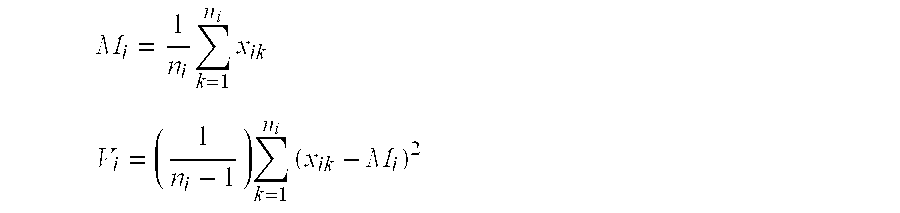
- where,
- data sets are designated as set j and run/wafer i;
- M i is the mean; and
- V i is the variance.
- The mean and variance values can be calculated using a portion or all of the population of the measurements collected for the run/wafer i. The set i corresponds to data which is a subset of the total measurements performed, defined as x ik where k=1, . . . , ni, with ni being the fraction of the total data collected for the run/wafer i.
- Since in most semiconductor manufacturing processes the variation of the metrology scales with the average value, a scaling operation (i.e., dividing the variance by a squared mean) can be performed and stored as a scaled variance, D i. However, a check is performed before the scaling operation to determine if the mean is too small to perform a scaling operation, e.g., a half of a squared mean value is smaller than the variance (step 705). If the scaling is performed, a register called “FLAG” is set to one (step 709). If the scaling is not performed, the “FLAG” register and the scaled variance are set to zero (step 707). The following is a set of equations describing these features:
- if (V i<M2 i/2)
- FLAG=1

- else
- D i=0
- FLAG=0
- The
estimator 405 then calculates a filtered estimate of the Di and Vi, which are designated as Di+1 f and Vf i+1, respectively (step 711). One example filter is the EWMA. - if i=1
- D i+1 f=Di
- V i+1+Vi
- else
- D i+1 f=λ·min(Di+1, Di)+(1−λ)·Di f
- V i+1 f=λ·min (Vi+1, Vi)+(1−λ)·Vi f
- The
estimator 405 then calculates the standard deviation, σi. This value is calculated in two different ways based on to which value the “FLAG” was set (step 713). - if i=1
- if FLAG=1
- σ i={square root}{square root over (Di)}
- else
- σ i={square root}{square root over (Vi)}
- else
- if FLAG=1
- σ i={square root}{square root over (D)}i
- else
- σ i={square root}{square root over (V)}i
- The
estimator 405, which receives a reliability level from a user (step 715), calculates a sigma coefficient Kf, based on the reliability level. Theestimator 405 also calculates the median, Rji, of the measurement values (step 717). Using the median, Rji, for run/wafer i data set j, the sigma coefficient Kf, and the filtered estimate of the standard deviation σi, theestimator 405 calculates an interval (step 719). An example of the interval can be expressed as: - if FLAG=1
- R ji−KfσiRji≦xki<Rji+KfσiRji
- else
- R ji−Kfσi≦xki≦Rji+KfσiRji
- The
estimator 405 calculates the average of the set of measurement values that fall within the interval (step 721). Theestimator 405 replaces all measurements in set j that lie outside the interval with the average value, and sets these points to be outliers (step 723). Theestimator 405 then recalculates and stores the filtered estimate values (step 725). The value of X is configurable in a graphical user interface. - Although embodiments described above in connection with FIG. 7 have been separately described from the embodiments describe above in connection with FIGS. 5-6, it should be noted that features of these embodiments can be combined. For instance, when one or more metrology stations make a number of measurements on a processed wafer, these measurements can first undergo the calculations as illustrated in FIG. 7. Subsequently, the calculated averages are designated as data points, and then can undergo the processes as illustrated in FIGS. 5-6. Example embodiments of the present invention that combine the features mentioned above are described below in connection with FIGS. 8A and 8B.
- As illustrated in FIG. 8A, measurements that include the value of goodness-of-fit (GOF) are received from the metrology stations 403 (step 801). The
estimator 405 conducts a measurement outlier screening (step 803). This step is similar to the steps described above in connection with calculating an interval for the measurements; - however, in these embodiments, the GOF and statistical outlier limits for specifically controlled output are provided from memory ( 805). If all measurements are outside the interval, then the measurements are not used in calculating a feedback value (step 809). If all measurements are not outside the interval, then the
estimator 405 calculates the average value of the measurements that fall within the interval (step 811). Theestimator 405 then updates statistical information (step 813), which can then be stored as an array of statistical information for specific controlled output from previous runs (step 815). - The average value calculated in
step 811 is used as a data point. Theestimator 405 performs a data point outlier screen step, which determines whether the data point is a candidate outlier similar to the steps described above in connection with FIGS. 5-6. - Based on
step 817, theestimator 405 determines if the data point is an outlier. If it is an outlier, then the data point is not used in calculating a feedback value (step 825). A state of the data point is determined similar to the steps described above in connection withsteps estimator 405 stores the current state of the data point (step 823). If the data point is not an outlier, theestimator 405 performs a feedback value screening (step 827), which is similar to the threshold test described above in connection with FIGS. 5-6. Based on the feedback value screening, theestimator 405 determines whether the feedback value is within noise limits (step 829). If the feedback value is within the noise limits, then the feedback value is not communicated to the optimizer 407 (step 831). Otherwise, the feedback value is communicated to the optimizer (step 833). Regardless of whether the feedback value falls within the noise limits, the estimator updates statistical information of relating to the data point (step 835). The resulting values are stored as statistical information for specific controlled output from previous runs to be used in performing the feedback outlier screening (step 837) and noise screening steps (step 839). - The results of performing the above-described embodiments of the present invention are graphically illustrated in FIG. 9. In particular, each data point represents a wafer being processed by Chemical Vapor Deposition (CVD). A metrology station collects thickness measurements of the processed wafers. For the measurements within normal operation, the average values of the measurements are used as the data points. When the measurements are out of range 907 (e.g., above a threshold value set to detect catastrophic cases), then the tool is halted and a message (e.g., an e-mail message and/or page) is sent to an operator. Moreover, such a set of measurements is not used in calculating a feedback value. When one of the measurements is out of an interval (e.g., 905), then the measurement is replaced with the average of the measurements within the interval and the filter values are stored.
- Embodiments of the present invention can be implemented as a set of computer executable codes (e.g., computer programs), implemented using computer hardware, or any combination of them. In particular, embodiments of the present invention are described in terms of various flow charts as shown in FIGS. 5-8A, B. Various acts depicted in the flow charts can be implemented as codes in computer programs or using computer hardware.
- Now turning to describe the software implemented embodiments of the present invention, FIG. 10 illustrates a block diagram of such embodiments. A
bus 1056 serves as the main information highway interconnecting various components.CPU 1058 is the central processing unit, performing calculations and logic operations required to execute the processes of the present invention as well as other programs. Read only memory (ROM) 1060 and random access memory (RAM) 1062 constitute the main memory.Disk controller 1064 interfaces one or more disk drives to thesystem bus 1056. These disk drives are, for example,floppy disk drives 1070, or CD ROM or DVD (digital video disks) drives 1066, or internal or external hard drives 1068. These various disk drives and disk controllers are optional devices. - A
display interface 1072 interfaces display 1048 and permits information from thebus 1056 to be displayed on display 1048. Communications with external devices such as the other components of the system described above, occur utilizing, for example,communication port 1074. Optical fibers and/or electrical cables and/or conductors and/or optical communication (e.g., infrared, and the like) and/or wireless communication (e.g., radio frequency (RF), and the like) can be used as the transport medium between the external devices andcommunication port 1074.Peripheral interface 1054 interfaces thekeyboard 1050 andmouse 1052, permitting input data to be transmitted tobus 1056. In addition to these components, the analyzer also optionally includes an infrared transmitter and/or infrared receiver. Infrared transmitters are optionally utilized when the computer system is used in conjunction with one or more of the processing components/stations that transmits/receives data via infrared signal transmission. Instead of utilizing an infrared transmitter or infrared receiver, the computer system may also optionally use a lowpower radio transmitter 1080 and/or a lowpower radio receiver 1082. The low power radio transmitter transmits the signal for reception by components of the production process, and receives signals from the components via the low power radio receiver. The low power radio transmitter and/or receiver are standard devices in the industry. - Although the embodiments depicted in FIG. 10 are illustrated having a single processor, a single hard disk drive and a single local memory, the analyzer is optionally suitably equipped with any multitude or combination of processors or storage devices. For example, the various embodiments may be replaced by, or combined with, any suitable processing system operative in accordance with the principles of embodiments of the present invention, including sophisticated calculators, and hand-held, laptop/notebook, mini, mainframe and super computers, as well as processing system network combinations of the same.
- Computer readable memory medium stores computer readable code or instructions. As one example, the medium may be used with disk drives illustrated in FIG. 10. Typically, memory media such as a CD ROM, a digital video disk, or floppy disks will contain, for example, a multi-byte locale for a single byte language and the program information for controlling the modeler to enable the computer to perform the functions described herein. Alternatively,
ROM 1060 and/orRAM 1062 illustrated in FIG. 10 can also be used to store the program information that is used to instruct thecentral processing unit 1058 to perform the operations associated with various automated processes of the present invention. Other examples of suitable computer readable media for storing information include magnetic, electronic, or optical (including holographic) storage, some combination thereof, etc. - In general, it should be emphasized that the various components of embodiments of the present invention can be implemented in hardware, software or a combination thereof. In such embodiments, the various components and steps would be implemented in hardware and/or software to perform the functions of embodiments of the present invention. Any presently available or future developed computer software language and/or hardware components can be employed in such embodiments of the present invention. For example, at least some of the functionality mentioned above could be implemented using Visual Basic, C, C++, or any computer language appropriate in view of the processor(s) being used. It could also be written in an interpretive environment such as Java and transported to multiple destinations to various users.
- The many features and advantages of embodiments of the present invention are apparent from the detailed specification, and thus, it is intended by the appended claims to cover all such features and advantages of the invention, which fall within the true spirit, and scope of the invention. Further, since numerous modifications and variations will readily occur to those skilled in the art, it is not desired to limit the invention to the exact construction and operation illustrated and described, and accordingly, all suitable modifications and equivalents may be resorted to, falling within the scope of the invention.
Claims (68)
1. A method of controlling a semiconductor manufacturing tool using a feedback control mechanism, comprising:
(a) receiving a plurality of data points relating to an output of the tool including a current data point and at least one previous data point;
(b) determining whether the current data point is an outlier based on:
(b-1) comparing the current data point to a statistical representation of the at least one previous data point; and
(b-2) whether the at least one previous data point is an outlier; and
(c) disregarding the current data point in calculating a feedback value of the feedback control mechanism if the current data point is determined as an outlier.
2. The method of claim 1 , wherein (b) further comprises:
determining the current data point as an outlier only if the at least one previous data point is not an outlier.
3. The method of claim 1 or 2, further comprising:
(d) calculating the feedback value of the feedback control mechanism using the current data point and the at least one previous data point if the current data point is determined as not an outlier.
4. The method of claim 1 or 2, further comprising:
(d) calculating a previous feedback value for the at least one previous data point and then calculating the feedback value based on the previous feedback value and the current data point if the at least one previous data point is an outlier and the current data point is an outlier.
5. The method of claim 1 or 2, wherein the statistical representation of (b-1) is a weighted moving average of the at least one previous data point.
6. The method of claim 1 or 2, wherein the statistical representation of (b-I) is an exponentially-weighted moving average of the at least one previous data point.
7. The method of claim 1 or 2, wherein the statistical representation of (b-1) is expressed as:
Sk=β(Fk−Δk)2+(1−β)Sk−1
where,
β is a coefficient;
Fk is the difference between the current data point and predicted values for wafer k; and
Δk is a feedback value for time k.
8. The method of claim 7 , wherein the value of Ak is calculated as:
if |Fk−Δk≦Knsk
Δk+1=λkFk+(1-λk)Δk
else
Δk+1=Δk
where, λk is a coefficient;
Kn is an outlier coefficient; and
sk={square root}{square root over (Sk)}.
9. The method of claim 7 , further comprising:
updating Sk as Sk=β(Fk−Δk)2+(1−β)Sk-1when the current data point is determined as not an outlier.
10. The method of claim 7 , further comprising:
updating Sk as Sk=Sk-1when the current data point is determined as an outlier.
11. The method of claim 6 , further comprising:
updating Sk as Sk-1=β(Fk−1−Δk−1)2+(1−β)Sk-1; and then
updating Sk as Sk=β(Fk−Δk)2+(1−β)Sk-1, when the current data point is determined as not an outlier and the previous data was not determined as an outliner.
12. The method of claim 1 or 2, further comprising:
making a plurality of measurements on the output of the tool using at least one metrology station; and
calculating the current data point based on the plurality of measurements.
13. The method of claim 12 , further comprising:
calculating an interval based on statistical information relating to the plurality of measurements;
identifying a subset among the plurality of measurements that fall within the interval; and
calculating the current data point from the subset of the plurality of the measurements.
14. The method of claim 13 , wherein the statistical information relates to at least one of a median and a standard deviation of the plurality of measurements.
15. The method of claim 14 , further comprising:
calculating the standard deviation based on one of a variance and a scaled variance of the plurality of measurements.
16. A system of controlling a semiconductor manufacturing tool using a feedback control mechanism, comprising:
an estimator configured to receive a plurality of data points relating to an output of the tool including a current data point and at least one previous data point,
wherein the estimator is further configured to determine whether the current data point is an outlier based on comparing the current data point to a statistical representation of the at least one previous data point, and whether the at least one previous data point is an outlier, and
wherein the estimator is further configured to disregard the current data point in calculating a feedback value of the feedback control mechanism if the current data point is determined as an outlier.
17. The system of claim 16 , wherein the estimator is further configure to determine the current data point as an outlier only if the at least one previous data point is an outlier.
18. The system of claim 16 , wherein the estimator is further configured to calculate the feedback value of the feedback control mechanism using the current data point and the at least one previous data point if the current data point is determined as not an outlier.
19. The system of claim 16 , wherein the estimator is further configured to calculate a previous feedback value for the at least one previous data point and then calculate the feedback value based on the previous feedback value and the current data point if the at least one previous data point is an outlier and the current data point is an outlier.
20. The system of claim 16 , wherein the statistical representation of is a weighted moving average of the at least one previous data point.
21. The system of claim 16 , wherein the statistical representation of is an exponentially-weighted moving average of the at least one previous data point.
22. The system of claim 16 , wherein the statistical representation of is expressed as:
Sk=β(Fk−Δk)2+(1−β)Sk-1
where,
β is a coefficient;
Fk is the difference between the current data point and predicted values for wafer k; and
Δk is a feedback value for time k.
23. The system of claim 22 , wherein the value of Δk is calculated as:
if |Fk−Δk|≦Knsk
Δk+1=λkFk+(1−λk)Δk
else Δk+1=Δk
where, λk is a coefficient;
Kn is an outlier coefficient; and
sk={square root}{square root over (Sk)}.
24. The system of claim 22 , wherein the estimator is further configured to update Sk as Sk=β(Fk−Δk)2+(1−β)Sk−1 when the current data point is determined as not an outlier.
25. The system of claim 22 , wherein the estimator is further configured to update Sk as Sk=Sk−1 when the current data point is determined as an outlier.
26. The system of claim 22 , wherein the estimator is further configured to update
Sk as Sk−1=β(Fk−1−Δk−1)2+(1−β)Sk−1; and
Sk as Sk=β(Fk−Δk)2+(1−β)Sk−1, when the current data point is determined as not an outlier and the previous data was not determined as an outliner.
27. The system of claim 16 , further comprising:
at least one metrology station configured to make a plurality of measurements on the output of the tool, wherein the estimator is further configured to calculate the current data point based on the plurality of measurements.
28. The system of claim 27 , the estimator is further configured to calculate an interval based on statistical information relating to the plurality of measurements, configured to identify a subset among the plurality of measurements that fall within the interval, and configured to calculate the current data point from the subset of the plurality of the measurements.
29. The system of claim 28 , wherein the statistical information relates to at least one of a median and a standard deviation of the plurality of measurements.
30. The system of claim 29 , the estimator is further configured to calculate the standard deviation based on one of a variance and a scaled variance of the plurality of measurements.
31. A system of controlling a semiconductor manufacturing tool using a feedback control mechanism, comprising:
(a) means for receiving a plurality of data points relating to an output of the tool including a current data point and at least one previous data point, where in the at least one previous data point is received before the current data point;
(b) means for determining whether the current data point is an outlier based on:
(b-1) comparing the current data point to a statistical representation of the at least one previous data point; and
(b-2) whether the at least one previous data point is an outlier; and
(c) means for disregarding the current data point in calculating a feedback value of the feedback control mechanism if the current data point is determined as an outlier.
32. The method of claim 31 , further comprising:
means for determining the current data point as an outlier only if the at least one previous data point is an outlier.
33. The system of claim 31 , further comprising:
(d) means for calculating the feedback value of the feedback control mechanism using the current data point and the at least one previous data point if the current data point is determined as not an outlier.
34. The system of claim 31 , further comprising:
(d) means for calculating a previous feedback value for the at least one previous data point and then calculating the feedback value based on the previous feedback value and the current data point if the at least one previous data point is an outlier and the current data point is an outlier.
35. The system of claim 31 , wherein the statistical representation of is a weighted moving average of the at least one previous data point.
36. The system of claim 31 , wherein the statistical representation of is an exponentially-weighted moving average of the at least one previous data point.
37. The system of claim 31 , wherein the statistical representation of is expressed as:
Sk=β(Fk−Δk)2+(1−β)Sk−1
where,
β is a coefficient;
Fk is the difference between the current data point and predicted values for wafer k; and
Δk is a feedback value for time k.
38. The system of claim 37 , wherein the value of Δk is calculated as:
if |Fk−Δk|≦Knsk
Δk+1=λkFk+(1−λk)Δk
else
Δk+1Δk
where, λk is a coefficient;
Kn is an outlier coefficient; and
sk={square root}{square root over (Sk)}.
39. The system of claim 39 , further comprising:
means for updating Sk as Sk=β(Fk−Δk)2+(1−β)Sk-1 when the current data point is determined as not an outlier.
40. The system of claim 37 , further comprising:
means for updating Sk as Sk=Sk-1 when the current data point is determined as an outlier.
41. The system of claim 37 , further comprising:
means for updating Sk as Sk−1=β(Fk−1−Δk−1)2+(1−β)Sk−1; and then
means for updating Sk as Sk=β(Fk−Δk)2+(1−β)Sk−1, when the current data point is determined as not an outlier and the previous data was not determined as an outliner.
42. The system of claim 31 , further comprising:
means for making a plurality of measurements on the output of the tool using at least one metrology station; and
means for calculating the current data point based on the plurality of measurements.
43. The system of claim 42 , further comprising:
means for calculating an interval based on statistical information relating to the plurality of measurements;
means for identifying a subset among the plurality of measurements that fall within the interval; and
means for calculating the current data point from the subset of the plurality of the measurements.
44. The system of claim 43 , wherein the statistical information relates to at least one of a median and a standard deviation of the plurality of measurements.
45. The system of claim 44 , further comprising:
means for calculating the standard deviation based on one of a variance and a scaled variance of the plurality of measurements.
46. A computer readable medium for storing instructions being executed by one or more computers, the instructions directing the one or more computers for controlling a semiconductor manufacturing tool using a feedback control mechanism, the instructions comprising implementation of the steps of:
(a) receiving a plurality of data points relating to an output of the tool including a current data point and at least one previous data point;
(b) determining whether the current data point is an outlier based on:
(b-1) comparing the current data point to a statistical representation of the at least one previous data point; and
(b-2) whether the at least one previous data point is an outlier; and
(c) disregarding the current data point in calculating a feedback value of the feedback control mechanism if the current data point is determined as an outlier.
47. The method of claim 46 , further comprising:
determining the current data point as an outlier only if the at least one previous data point is an outlier.
48. The medium of claim 46 , further comprising:
(d) calculating the feedback value of the feedback control mechanism using the current data point and the at least one previous data point if the current data point is determined as not an outlier.
49. The medium of claim 46 , further comprising:
(d) calculating a previous feedback value for the at least one previous data point and then calculating the feedback value based on the previous feedback value and the current data point if the at least one previous data point is an outlier and the current data point is an outlier.
50. The medium of claim 46 , wherein the statistical representation of (b-1) is a weighted moving average of the at least one previous data point.
51. The medium of claim 46 , wherein the statistical representation of (b-I) is an exponentially-weighted moving average of the at least one previous data point.
52. The medium of claim 46 , wherein the statistical representation of (b-1) is expressed as:
Sk=β(Fk−Δk)2+(1−β)Sk−1
where,
β is a coefficient;
Fk is the difference between the current data point and predicted values for wafer k; and
Δk is a feedback value for time k.
53. The medium of claim 52 , wherein the value of Δk is calculated as:
if |Fk−Δk|≦Knsk
Δk+1=λkFk+(1−λk)Δk
else
Δk+1=Δk
where, λk is a coefficient;
Kn is an outlier coefficient; and
Sk={square root}{square root over (Sk)}.
54. The medium of claim 52 , further comprising:
updating Sk as Sk=β(Fk−Δk)2+(1−β)Sk−1 when the current data point is determined as not an outlier.
55. The medium of claim 52 , further comprising:
updating Sk as Sk=Sk−1 when the current data point is determined as an outlier.
56. The medium of claim 52 , further comprising:
updating Sk as Sk-1=β(Fk−1−Δk−1)2+(1−β)Sk−1; and then
updating Sk as Sk=β(Fk−Δk)2+(1−β)Sk−1, when the current data point is determined as not an outlier and the previous data was not determined as an outliner.
57. The medium of claim 46 , further comprising:
making a plurality of measurements on the output of the tool using at least one metrology station; and
calculating the current data point based on the plurality of measurements.
58. The medium of claim 57 , further comprising:
calculating an interval based on statistical information relating to the plurality of measurements;
identifying a subset among the plurality of measurements that fall within the interval; and
calculating the current data point from the subset of the plurality of the measurements.
59. The medium of claim 58 , wherein the statistical information relates to at least one of a median and a standard deviation of the plurality of measurements.
60. The medium of claim 59 , further comprising:
calculating the standard deviation based on one of a variance and a scaled variance of the plurality of measurements.
61. A system of manufacturing semiconductor devices using a feedback control mechanism, comprising:
at least one processing tool configured to perform at least one semiconductor fabrication step on at least one wafer;
at least one metrology station coupled to the at least one processing tool and configured to make measurements on the at least one wafer;
an estimator configured to receive a plurality of data points relating to an output of the at least one tool including a current data point and at least one previous data point calculated base on the measurements made by the at least one metrology station,
wherein the estimator is further configured to determine whether the current data point is an outlier based on comparing the current data point to a statistical representation of the at least one previous data point, and whether the at least one previous data point is an outlier, and
wherein the estimator is further configured to disregard the current data point in calculating a feedback value of the feedback control mechanism if the current data point is determined as an outlier.
62. The system of claim 61 , wherein the estimator is further configure to determine the current data point as an outlier only if the at least one previous data point is an outlier.
63. The system of claim 61 , further comprising:
an optimizer coupled to the estimator to receive the feedback value and configured to generate at least one control parameter for operating the at least one tool based on the feedback value.
64. The system of claim 61 , wherein the at least one tool is an etcher.
65. A method of controlling a semiconductor manufacturing tool using a feedback control mechanism, comprising:
(a) receiving a plurality of data points relating to an output of the tool including a current data point, a subsequent data point, and at least one previous data point;
(b) determining the current data point as an erroneous outlier:
(b-1) if a difference between the current data point and a predicted value, which is calculated from a statistical representation of the at least one previous data point, is outside of a threshold;
(b-2) if the at least one previous data point is not an outlier; and
(b-3) if the subsequent data point is not an outlier; and
(c) disregarding the current data point in calculating a feedback value of the feedback control mechanism if the current data point is determined as an erroneous outlier.
66. The method of claim 65 , wherein the statistical representation of (b-1) is an exponentially-weighted moving average of the at least one previous data point.
67. The method of claim 66 , wherein the statistical representation of (b-1) is expressed as:
Sk=β(Fk−Δk)2+(1−β)Sk−1
where,
β is a coefficient;
Fk is the difference between the current data point and predicted values for wafer k; and
Δk is a feedback value for time k.
68. The method of claim 67 , wherein the threshold is calculated as:
|Fk−Δk|≦Knsk
where, λk is a coefficient;
Kn is an outlier coefficient; and
sk={square root}{square root over (Sk)}.
Priority Applications (1)
| Application Number | Priority Date | Filing Date | Title |
|---|---|---|---|
| US10/632,107 US6999836B2 (en) | 2002-08-01 | 2003-08-01 | Method, system, and medium for handling misrepresentative metrology data within an advanced process control system |
Applications Claiming Priority (2)
| Application Number | Priority Date | Filing Date | Title |
|---|---|---|---|
| US39969502P | 2002-08-01 | 2002-08-01 | |
| US10/632,107 US6999836B2 (en) | 2002-08-01 | 2003-08-01 | Method, system, and medium for handling misrepresentative metrology data within an advanced process control system |
Publications (2)
| Publication Number | Publication Date |
|---|---|
| US20040143357A1 true US20040143357A1 (en) | 2004-07-22 |
| US6999836B2 US6999836B2 (en) | 2006-02-14 |
Family
ID=31495751
Family Applications (1)
| Application Number | Title | Priority Date | Filing Date |
|---|---|---|---|
| US10/632,107 Expired - Fee Related US6999836B2 (en) | 2002-08-01 | 2003-08-01 | Method, system, and medium for handling misrepresentative metrology data within an advanced process control system |
Country Status (7)
| Country | Link |
|---|---|
| US (1) | US6999836B2 (en) |
| EP (1) | EP1546828A1 (en) |
| JP (1) | JP2005535130A (en) |
| KR (1) | KR20050026099A (en) |
| CN (1) | CN100351725C (en) |
| AU (1) | AU2003254283A1 (en) |
| WO (1) | WO2004013715A1 (en) |
Cited By (8)
| Publication number | Priority date | Publication date | Assignee | Title |
|---|---|---|---|---|
| US6917849B1 (en) * | 2002-12-18 | 2005-07-12 | Advanced Micro Devices, Inc. | Method and apparatus for predicting electrical parameters using measured and predicted fabrication parameters |
| US20070094196A1 (en) * | 2005-09-14 | 2007-04-26 | Fujitsu Limited | Manufacture data analysis method and manufacture data analyzer apparatus |
| CN103092074A (en) * | 2012-12-30 | 2013-05-08 | 重庆邮电大学 | Parameter optimization control method of semiconductor advance process control |
| US20130178989A1 (en) * | 2012-01-11 | 2013-07-11 | Hamilton Sundstrand Corporation | Air temperature controller |
| US20150162166A1 (en) * | 2013-12-06 | 2015-06-11 | Taiwan Semiconductor Manufacturing Co., Ltd. | System and method for controlling ion implanter |
| US10239635B2 (en) * | 2017-06-08 | 2019-03-26 | The Boeing Company | Methods for balancing aircraft engines based on flight data |
| US20190108422A1 (en) * | 2017-10-05 | 2019-04-11 | Applied Materials, Inc. | Fault detection classification |
| WO2019075217A1 (en) | 2017-10-11 | 2019-04-18 | Littelfuse, Inc. | Arc detection based on variance of current flow |
Families Citing this family (40)
| Publication number | Priority date | Publication date | Assignee | Title |
|---|---|---|---|---|
| US6863771B2 (en) * | 2001-07-25 | 2005-03-08 | Micron Technology, Inc. | Differential pressure application apparatus for use in polishing layers of semiconductor device structures and methods |
| US7545531B2 (en) * | 2004-05-18 | 2009-06-09 | Xerox Corporation | Method and apparatus for implementing statistical process control (SPC) in a printing environment |
| US20060129257A1 (en) * | 2004-12-13 | 2006-06-15 | Taiwan Semiconductor Manufacturing Co., Ltd. | Novel method and apparatus for integrating fault detection and real-time virtual metrology in an advanced process control framework |
| US7477958B2 (en) * | 2005-05-11 | 2009-01-13 | International Business Machines Corporation | Method of release and product flow management for a manufacturing facility |
| US7359759B2 (en) * | 2005-10-31 | 2008-04-15 | Taiwan Semiconductor Manufacturing Company | Method and system for virtual metrology in semiconductor manufacturing |
| US7200523B1 (en) * | 2005-11-30 | 2007-04-03 | Taiwan Semiconductor Manufacturing Company, Ltd. | Method and system for filtering statistical process data to enhance process performance |
| US7536371B2 (en) * | 2005-12-05 | 2009-05-19 | Insyst Ltd. | Apparatus and method for the analysis of a process having parameter-based faults |
| US7292959B1 (en) * | 2006-01-30 | 2007-11-06 | Advanced Mirco Devices, Inc. | Total tool control for semiconductor manufacturing |
| US7522968B2 (en) * | 2006-07-10 | 2009-04-21 | Applied Materials, Inc. | Scheduling method for processing equipment |
| US20080051930A1 (en) * | 2006-07-10 | 2008-02-28 | Oh Hilario L | Scheduling method for processing equipment |
| WO2008008727A2 (en) * | 2006-07-10 | 2008-01-17 | Applied Materials, Inc. | Scheduling method for processing equipment |
| US7899627B2 (en) * | 2006-09-28 | 2011-03-01 | Lam Research Corporation | Automatic dynamic baseline creation and adjustment |
| JP5242906B2 (en) * | 2006-10-17 | 2013-07-24 | 東京エレクトロン株式会社 | Substrate processing apparatus control device, control method, and storage medium storing control program |
| JP2009008072A (en) * | 2007-05-30 | 2009-01-15 | Yamaha Motor Co Ltd | Running controlling apparatus and ship including the same |
| US20080319565A1 (en) * | 2007-06-25 | 2008-12-25 | International Business Machines Corporation | System and methods for managing process flow changes |
| JP5117818B2 (en) | 2007-10-30 | 2013-01-16 | ルネサスエレクトロニクス株式会社 | Management apparatus and method for foreign matter inspection / analysis of surface processing apparatus or film forming apparatus |
| US20090200674A1 (en) * | 2008-02-07 | 2009-08-13 | International Business Machines Corporation | Structure and method of forming transitional contacts between wide and thin beol wirings |
| US8269960B2 (en) | 2008-07-24 | 2012-09-18 | Kla-Tencor Corp. | Computer-implemented methods for inspecting and/or classifying a wafer |
| US8229588B2 (en) * | 2009-03-03 | 2012-07-24 | Taiwan Semiconductor Manufacturing Company, Ltd. | Method and system for tuning advanced process control parameters |
| US8073556B2 (en) | 2009-12-16 | 2011-12-06 | General Electric Company | System and method for controlling a machine |
| US8670857B2 (en) * | 2010-02-02 | 2014-03-11 | Applied Materials, Inc. | Flexible process condition monitoring |
| JP5600503B2 (en) * | 2010-07-06 | 2014-10-01 | 株式会社日立国際電気 | Statistical analysis method, substrate processing system, and program |
| US9052709B2 (en) * | 2010-07-30 | 2015-06-09 | Kla-Tencor Corporation | Method and system for providing process tool correctables |
| JP5855841B2 (en) | 2011-04-01 | 2016-02-09 | 株式会社日立国際電気 | Management device |
| US8420531B2 (en) | 2011-06-21 | 2013-04-16 | International Business Machines Corporation | Enhanced diffusion barrier for interconnect structures |
| US9146551B2 (en) * | 2012-11-29 | 2015-09-29 | Asm Ip Holding B.V. | Scheduler for processing system |
| US9070591B2 (en) * | 2012-12-24 | 2015-06-30 | Taiwan Semiconductor Manufacturing Company Limited | Adjusting intensity of laser beam during laser operation on a semiconductor device |
| US10289109B2 (en) * | 2015-10-01 | 2019-05-14 | Globalfoundries Inc. | Methods of error detection in fabrication processes |
| US9406617B1 (en) | 2015-11-19 | 2016-08-02 | International Business Machines Corporation | Structure and process for W contacts |
| US10177091B2 (en) | 2016-02-19 | 2019-01-08 | Globalfoundries Inc. | Interconnect structure and method of forming |
| US9761484B1 (en) | 2016-07-25 | 2017-09-12 | International Business Machines Corporation | Interconnect structure and fabrication thereof |
| US9773735B1 (en) | 2016-08-16 | 2017-09-26 | International Business Machines Corporation | Geometry control in advanced interconnect structures |
| US9953864B2 (en) | 2016-08-30 | 2018-04-24 | International Business Machines Corporation | Interconnect structure |
| US9768118B1 (en) | 2016-09-19 | 2017-09-19 | International Business Machines Corporation | Contact having self-aligned air gap spacers |
| US9786603B1 (en) | 2016-09-22 | 2017-10-10 | International Business Machines Corporation | Surface nitridation in metal interconnects |
| US9721895B1 (en) | 2016-10-06 | 2017-08-01 | International Business Machines Corporation | Self-formed liner for interconnect structures |
| JP6917879B2 (en) * | 2017-12-19 | 2021-08-11 | 株式会社日立ハイテク | Measuring device and measurement data processing method |
| US11133216B2 (en) | 2018-06-01 | 2021-09-28 | International Business Machines Corporation | Interconnect structure |
| US10916503B2 (en) | 2018-09-11 | 2021-02-09 | International Business Machines Corporation | Back end of line metallization structure |
| US10714382B2 (en) | 2018-10-11 | 2020-07-14 | International Business Machines Corporation | Controlling performance and reliability of conductive regions in a metallization network |
Citations (97)
| Publication number | Priority date | Publication date | Assignee | Title |
|---|---|---|---|---|
| US17256A (en) * | 1857-05-12 | Portable barrack | ||
| US640596A (en) * | 1899-05-12 | 1900-01-02 | Frank Henry Stahl | Automatic adjustable die. |
| US3229198A (en) * | 1962-09-28 | 1966-01-11 | Hugo L Libby | Eddy current nondestructive testing device for measuring multiple parameter variables of a metal sample |
| US4207520A (en) * | 1978-04-06 | 1980-06-10 | The United States Of America As Represented By The Secretary Of The Air Force | Multiple frequency digital eddy current inspection system |
| US4209744A (en) * | 1976-04-29 | 1980-06-24 | Fedosenko Jury K | Eddy current device for automatically testing the quality of elongated electrically conductive objects by non-destructive techniques |
| US4368510A (en) * | 1980-10-20 | 1983-01-11 | Leeds & Northrup Company | Automatic identification system for self tuning process controller |
| US4663703A (en) * | 1985-10-02 | 1987-05-05 | Westinghouse Electric Corp. | Predictive model reference adaptive controller |
| US4750141A (en) * | 1985-11-26 | 1988-06-07 | Ade Corporation | Method and apparatus for separating fixture-induced error from measured object characteristics and for compensating the measured object characteristic with the error, and a bow/warp station implementing same |
| US4796194A (en) * | 1986-08-20 | 1989-01-03 | Atherton Robert W | Real world modeling and control process |
| US4901218A (en) * | 1987-08-12 | 1990-02-13 | Renishaw Controls Limited | Communications adaptor for automated factory system |
| US5089970A (en) * | 1989-10-05 | 1992-02-18 | Combustion Engineering, Inc. | Integrated manufacturing system |
| US5108570A (en) * | 1990-03-30 | 1992-04-28 | Applied Materials, Inc. | Multistep sputtering process for forming aluminum layer over stepped semiconductor wafer |
| US5179495A (en) * | 1990-08-02 | 1993-01-12 | Furnas Electric Company | Solid state overload relay |
| US5208765A (en) * | 1990-07-20 | 1993-05-04 | Advanced Micro Devices, Inc. | Computer-based method and system for product development |
| US5220517A (en) * | 1990-08-31 | 1993-06-15 | Sci Systems, Inc. | Process gas distribution system and method with supervisory control |
| US5283141A (en) * | 1992-03-05 | 1994-02-01 | National Semiconductor | Photolithography control system and method using latent image measurements |
| US5295242A (en) * | 1990-11-02 | 1994-03-15 | Consilium, Inc. | Apparatus and method for viewing relationships in a factory management system |
| US5309221A (en) * | 1991-12-31 | 1994-05-03 | Corning Incorporated | Measurement of fiber diameters with high precision |
| US5398336A (en) * | 1990-10-16 | 1995-03-14 | Consilium, Inc. | Object-oriented architecture for factory floor management |
| US5402367A (en) * | 1993-07-19 | 1995-03-28 | Texas Instruments, Incorporated | Apparatus and method for model based process control |
| US5408405A (en) * | 1993-09-20 | 1995-04-18 | Texas Instruments Incorporated | Multi-variable statistical process controller for discrete manufacturing |
| US5410473A (en) * | 1992-01-07 | 1995-04-25 | Fukuda Denshi Kabushiki Kaisha | Method and apparatus for recording electrocardiogram information |
| US5420796A (en) * | 1993-12-23 | 1995-05-30 | Vlsi Technology, Inc. | Method of inspecting planarity of wafer surface after etchback step in integrated circuit fabrication |
| US5427878A (en) * | 1991-06-26 | 1995-06-27 | Digital Equipment Corporation | Semiconductor wafer processing with across-wafer critical dimension monitoring using optical endpoint detection |
| US5485082A (en) * | 1990-04-11 | 1996-01-16 | Micro-Epsilon Messtechnik Gmbh & Co. Kg | Method of calibrating a thickness measuring device and device for measuring or monitoring the thickness of layers, tapes, foils, and the like |
| US5490097A (en) * | 1993-03-22 | 1996-02-06 | Fujitsu Limited | System and method for modeling, analyzing and executing work process plans |
| US5495417A (en) * | 1990-08-14 | 1996-02-27 | Kabushiki Kaisha Toshiba | System for automatically producing different semiconductor products in different quantities through a plurality of processes along a production line |
| US5497381A (en) * | 1993-10-15 | 1996-03-05 | Analog Devices, Inc. | Bitstream defect analysis method for integrated circuits |
| US5506707A (en) * | 1993-07-30 | 1996-04-09 | Sony Corporation | Electrode substrate having double layers of indium tin oxide and method for making the same |
| US5511005A (en) * | 1994-02-16 | 1996-04-23 | Ade Corporation | Wafer handling and processing system |
| US5519605A (en) * | 1994-10-24 | 1996-05-21 | Olin Corporation | Model predictive control apparatus and method |
| US5525808A (en) * | 1992-01-23 | 1996-06-11 | Nikon Corporaton | Alignment method and alignment apparatus with a statistic calculation using a plurality of weighted coordinate positions |
| US5526293A (en) * | 1993-12-17 | 1996-06-11 | Texas Instruments Inc. | System and method for controlling semiconductor wafer processing |
| US5599423A (en) * | 1995-06-30 | 1997-02-04 | Applied Materials, Inc. | Apparatus and method for simulating and optimizing a chemical mechanical polishing system |
| US5602492A (en) * | 1992-03-13 | 1997-02-11 | The United States Of America As Represented By The Secretary Of Commerce | Electrical test structure and method for measuring the relative locations of conducting features on an insulating substrate |
| US5603707A (en) * | 1995-11-28 | 1997-02-18 | The Procter & Gamble Company | Absorbent article having a rewet barrier |
| US5617023A (en) * | 1995-02-02 | 1997-04-01 | Otis Elevator Company | Industrial contactless position sensor |
| US5627083A (en) * | 1993-08-03 | 1997-05-06 | Nec Corporation | Method of fabricating semiconductor device including step of forming superposition error measuring patterns |
| US5629216A (en) * | 1994-06-30 | 1997-05-13 | Seh America, Inc. | Method for producing semiconductor wafers with low light scattering anomalies |
| US5642296A (en) * | 1993-07-29 | 1997-06-24 | Texas Instruments Incorporated | Method of diagnosing malfunctions in semiconductor manufacturing equipment |
| US5719796A (en) * | 1995-12-04 | 1998-02-17 | Advanced Micro Devices, Inc. | System for monitoring and analyzing manufacturing processes using statistical simulation with single step feedback |
| US5737055A (en) * | 1996-08-22 | 1998-04-07 | Bausch & Lomb Incorporated | Nosepiece for eyewear |
| US5740429A (en) * | 1995-07-07 | 1998-04-14 | Advanced Micro Devices, Inc. | E10 reporting tool |
| US5751582A (en) * | 1995-09-25 | 1998-05-12 | Texas Instruments Incorporated | Controlling process modules using site models and monitor wafer control |
| US5754297A (en) * | 1994-01-28 | 1998-05-19 | Applied Materials, Inc. | Method and apparatus for monitoring the deposition rate of films during physical vapor deposition |
| US5761065A (en) * | 1995-03-30 | 1998-06-02 | Advanced Micro Devices, Inc. | Arrangement and method for detecting sequential processing effects in manufacturing |
| US5761064A (en) * | 1995-10-06 | 1998-06-02 | Advanced Micro Devices, Inc. | Defect management system for productivity and yield improvement |
| US5764543A (en) * | 1995-06-16 | 1998-06-09 | I2 Technologies, Inc. | Extensible model network representation system for process planning |
| US5859964A (en) * | 1996-10-25 | 1999-01-12 | Advanced Micro Devices, Inc. | System and method for performing real time data acquisition, process modeling and fault detection of wafer fabrication processes |
| US5859777A (en) * | 1996-05-14 | 1999-01-12 | Toshiba Kikai Kabushiki Kaisha | Casting control support system for die casting machines |
| US5857258A (en) * | 1992-03-13 | 1999-01-12 | The United States Of America As Represented By The Secretary Of Commerce | Electrical test structure and method for measuring the relative locations of conductive features on an insulating substrate |
| US5859975A (en) * | 1993-12-15 | 1999-01-12 | Hewlett-Packard, Co. | Parallel processing computer system having shared coherent memory and interconnections utilizing separate undirectional request and response lines for direct communication or using crossbar switching device |
| US5862054A (en) * | 1997-02-20 | 1999-01-19 | Taiwan Semiconductor Manufacturing Company, Ltd. | Process monitoring system for real time statistical process control |
| US5863807A (en) * | 1995-09-20 | 1999-01-26 | Samsung Electronics Co., Ltd. | Manufacturing method of a semiconductor integrated circuit |
| US5867389A (en) * | 1995-11-29 | 1999-02-02 | Dainippon Screen Mfg. Co., Ltd. | Substrate processing management system with recipe copying functions |
| US5870306A (en) * | 1996-06-13 | 1999-02-09 | Mitsubishi Denki Kabushiki Kaisha | Automatic programming method and device for multi-system machine tool |
| US5871805A (en) * | 1996-04-08 | 1999-02-16 | Lemelson; Jerome | Computer controlled vapor deposition processes |
| US5883437A (en) * | 1994-12-28 | 1999-03-16 | Hitachi, Ltd. | Method and apparatus for inspection and correction of wiring of electronic circuit and for manufacture thereof |
| US5889991A (en) * | 1996-12-06 | 1999-03-30 | International Business Machines Corp. | Method and system for customizing a palette using any java class |
| US5901313A (en) * | 1991-03-01 | 1999-05-04 | Ast Research, Inc. | Application management system |
| US5903455A (en) * | 1996-02-06 | 1999-05-11 | Fisher-Rosemount Systems, Inc. | Interface controls for use in a field device management system |
| US5910846A (en) * | 1996-05-16 | 1999-06-08 | Micron Technology, Inc. | Method and apparatus for detecting the endpoint in chemical-mechanical polishing of semiconductor wafers |
| US5910011A (en) * | 1997-05-12 | 1999-06-08 | Applied Materials, Inc. | Method and apparatus for monitoring processes using multiple parameters of a semiconductor wafer processing system |
| US5912678A (en) * | 1997-04-14 | 1999-06-15 | Texas Instruments Incorporated | Process flow design at the module effects level through the use of acceptability regions |
| US6012048A (en) * | 1997-05-30 | 2000-01-04 | Capital Security Systems, Inc. | Automated banking system for dispensing money orders, wire transfer and bill payment |
| US6037664A (en) * | 1997-08-20 | 2000-03-14 | Sematech Inc | Dual damascene interconnect structure using low dielectric constant material for an inter-level dielectric layer |
| US6059636A (en) * | 1997-07-11 | 2000-05-09 | Tokyo Seimitsu Co., Ltd. | Wafer polishing apparatus |
| US6181013B1 (en) * | 1999-06-25 | 2001-01-30 | Taiwan Semiconductor Manufacturing Company | Method for selective growth of Cu3Ge or Cu5Si for passivation of damascene copper structures and device manufactured thereby |
| US6212961B1 (en) * | 1999-02-11 | 2001-04-10 | Nova Measuring Instruments Ltd. | Buffer system for a wafer handling system |
| US6226563B1 (en) * | 1998-01-14 | 2001-05-01 | Samsung Electronics Co., Ltd. | Method for controlling unit process conditions of semiconductor fabricating equipment arranged in a processing line |
| US6228280B1 (en) * | 1998-05-06 | 2001-05-08 | International Business Machines Corporation | Endpoint detection by chemical reaction and reagent |
| US6226961B1 (en) * | 1998-08-07 | 2001-05-08 | Gigi C. Gordon | Cleaning articles |
| US6230069B1 (en) * | 1998-06-26 | 2001-05-08 | Advanced Micro Devices, Inc. | System and method for controlling the manufacture of discrete parts in semiconductor fabrication using model predictive control |
| US6237050B1 (en) * | 1997-12-26 | 2001-05-22 | Samsung Electronics Co., Ltd. | Method for controlling components of semiconductor fabricating equipment arranged in a processing line |
| US6339727B1 (en) * | 1998-12-21 | 2002-01-15 | Recot, Inc. | Apparatus and method for controlling distribution of product in manufacturing process |
| US6346426B1 (en) * | 2000-11-17 | 2002-02-12 | Advanced Micro Devices, Inc. | Method and apparatus for characterizing semiconductor device performance variations based on independent critical dimension measurements |
| US6355559B1 (en) * | 1999-11-18 | 2002-03-12 | Texas Instruments Incorporated | Passivation of inlaid metallization |
| US6368883B1 (en) * | 1999-08-10 | 2002-04-09 | Advanced Micro Devices, Inc. | Method for identifying and controlling impact of ambient conditions on photolithography processes |
| US6368884B1 (en) * | 2000-04-13 | 2002-04-09 | Advanced Micro Devices, Inc. | Die-based in-fab process monitoring and analysis system for semiconductor processing |
| US6381564B1 (en) * | 1998-05-28 | 2002-04-30 | Texas Instruments Incorporated | Method and system for using response-surface methodologies to determine optimal tuning parameters for complex simulators |
| US6391780B1 (en) * | 1999-08-23 | 2002-05-21 | Taiwan Semiconductor Manufacturing Company | Method to prevent copper CMP dishing |
| US6515368B1 (en) * | 2001-12-07 | 2003-02-04 | Advanced Micro Devices, Inc. | Semiconductor device with copper-filled via includes a copper-zinc/alloy film for reduced electromigration of copper |
| US6517414B1 (en) * | 2000-03-10 | 2003-02-11 | Appied Materials, Inc. | Method and apparatus for controlling a pad conditioning process of a chemical-mechanical polishing apparatus |
| US6529789B1 (en) * | 1999-06-17 | 2003-03-04 | Advanced Micro Devices, Inc. | Method and apparatus for automatic routing for reentrant processes |
| US6528409B1 (en) * | 2002-04-29 | 2003-03-04 | Advanced Micro Devices, Inc. | Interconnect structure formed in porous dielectric material with minimized degradation and electromigration |
| US6532555B1 (en) * | 1999-10-29 | 2003-03-11 | Advanced Micro Devices, Inc. | Method and apparatus for integration of real-time tool data and in-line metrology for fault detection in an advanced process control (APC) framework |
| US6535783B1 (en) * | 2001-03-05 | 2003-03-18 | Advanced Micro Devices, Inc. | Method and apparatus for the integration of sensor data from a process tool in an advanced process control (APC) framework |
| US6537912B1 (en) * | 2000-08-25 | 2003-03-25 | Micron Technology Inc. | Method of forming an encapsulated conductive pillar |
| US6541401B1 (en) * | 2000-07-31 | 2003-04-01 | Applied Materials, Inc. | Wafer pretreatment to decrease rate of silicon dioxide deposition on silicon nitride compared to silicon substrate |
| US6546508B1 (en) * | 1999-10-29 | 2003-04-08 | Advanced Micro Devices, Inc. | Method and apparatus for fault detection of a processing tool in an advanced process control (APC) framework |
| US6556881B1 (en) * | 1999-09-09 | 2003-04-29 | Advanced Micro Devices, Inc. | Method and apparatus for integrating near real-time fault detection in an APC framework |
| US6678570B1 (en) * | 2001-06-26 | 2004-01-13 | Advanced Micro Devices, Inc. | Method and apparatus for determining output characteristics using tool state data |
| US6708074B1 (en) * | 2000-08-11 | 2004-03-16 | Applied Materials, Inc. | Generic interface builder |
| US6708075B2 (en) * | 2001-11-16 | 2004-03-16 | Advanced Micro Devices | Method and apparatus for utilizing integrated metrology data as feed-forward data |
| US6725402B1 (en) * | 2000-07-31 | 2004-04-20 | Advanced Micro Devices, Inc. | Method and apparatus for fault detection of a processing tool and control thereof using an advanced process control (APC) framework |
| US6728587B2 (en) * | 2000-12-27 | 2004-04-27 | Insyst Ltd. | Method for global automated process control |
| US6735492B2 (en) * | 2002-07-19 | 2004-05-11 | International Business Machines Corporation | Feedback method utilizing lithographic exposure field dimensions to predict process tool overlay settings |
Family Cites Families (56)
| Publication number | Priority date | Publication date | Assignee | Title |
|---|---|---|---|---|
| US3205485A (en) | 1960-10-21 | 1965-09-07 | Ti Group Services Ltd | Screening vane electro-mechanical transducer |
| US3767900A (en) | 1971-06-23 | 1973-10-23 | Cons Paper Inc | Adaptive controller having optimal filtering |
| CH569321A5 (en) | 1973-10-03 | 1975-11-14 | Siemens Ag | |
| US4000458A (en) | 1975-08-21 | 1976-12-28 | Bell Telephone Laboratories, Incorporated | Method for the noncontacting measurement of the electrical conductivity of a lamella |
| US4302721A (en) | 1978-05-08 | 1981-11-24 | Tencor Instruments | Non-contacting resistivity instrument with structurally related conductance and distance measuring transducers |
| US4609870A (en) | 1981-03-27 | 1986-09-02 | Hocking Electronics Limited | Lift off compensation of eddy current crack detection system by controlling damping resistance of oscillator |
| US4616308A (en) | 1983-11-15 | 1986-10-07 | Shell Oil Company | Dynamic process control |
| DE3581000D1 (en) | 1984-05-19 | 1991-02-07 | British Aerospace | INDUSTRIAL PROCESSING AND MANUFACTURING PROCESSES. |
| US4967381A (en) | 1985-04-30 | 1990-10-30 | Prometrix Corporation | Process control interface system for managing measurement data |
| FR2589566A1 (en) | 1985-11-06 | 1987-05-07 | Cegedur | METHOD FOR NON-CONTACT SCALE MEASUREMENT OF THE THICKNESS AND TEMPERATURE OF THIN METAL SHEETS USING FOUCAULT CURRENTS |
| US4755753A (en) | 1986-07-23 | 1988-07-05 | General Electric Company | Eddy current surface mapping system for flaw detection |
| US5260868A (en) | 1986-08-11 | 1993-11-09 | Texas Instruments Incorporate | Method for calendaring future events in real-time |
| US5016186A (en) * | 1988-02-09 | 1991-05-14 | Mitsubishi Jukogyo Kabushiki Kaisha | Method of detecting noise disappearance and detecting device therefor |
| US4938600A (en) | 1989-02-09 | 1990-07-03 | Interactive Video Systems, Inc. | Method and apparatus for measuring registration between layers of a semiconductor wafer |
| US4957605A (en) | 1989-04-17 | 1990-09-18 | Materials Research Corporation | Method and apparatus for sputter coating stepped wafers |
| JP2780814B2 (en) | 1989-06-22 | 1998-07-30 | 株式会社日立製作所 | production management system |
| US5236868A (en) | 1990-04-20 | 1993-08-17 | Applied Materials, Inc. | Formation of titanium nitride on semiconductor wafer by reaction of titanium with nitrogen-bearing gas in an integrated processing system |
| US5270222A (en) | 1990-12-31 | 1993-12-14 | Texas Instruments Incorporated | Method and apparatus for semiconductor device fabrication diagnosis and prognosis |
| US5226118A (en) | 1991-01-29 | 1993-07-06 | Prometrix Corporation | Data analysis system and method for industrial process control systems |
| US5347446A (en) | 1991-02-08 | 1994-09-13 | Kabushiki Kaisha Toshiba | Model predictive control apparatus |
| US5469361A (en) | 1991-08-08 | 1995-11-21 | The Board Of Regents Acting For And On Behalf Of The University Of Michigan | Generic cell controlling method and apparatus for computer integrated manufacturing system |
| US5240552A (en) | 1991-12-11 | 1993-08-31 | Micron Technology, Inc. | Chemical mechanical planarization (CMP) of a semiconductor wafer using acoustical waves for in-situ end point detection |
| FR2700403B1 (en) | 1993-01-12 | 1995-04-07 | Sextant Avionique | Method for structuring information used in an industrial process and its application to assistance in piloting an aerodyne. |
| US5586039A (en) | 1993-03-29 | 1996-12-17 | Texas Instruments Incorporated | Computer-aided manufacturing support method and system for specifying relationships and dependencies between process type components |
| US5369544A (en) | 1993-04-05 | 1994-11-29 | Ford Motor Company | Silicon-on-insulator capacitive surface micromachined absolute pressure sensor |
| US5367624A (en) | 1993-06-11 | 1994-11-22 | Consilium, Inc. | Interface for controlling transactions in a manufacturing execution system |
| US5546312A (en) | 1993-09-20 | 1996-08-13 | Texas Instruments Incorporated | Use of spatial models for simultaneous control of various non-uniformity metrics |
| US5503707A (en) | 1993-09-22 | 1996-04-02 | Texas Instruments Incorporated | Method and apparatus for process endpoint prediction based on actual thickness measurements |
| DE69425100T2 (en) | 1993-09-30 | 2001-03-15 | Koninkl Philips Electronics Nv | Dynamic neural network |
| US5375064A (en) | 1993-12-02 | 1994-12-20 | Hughes Aircraft Company | Method and apparatus for moving a material removal tool with low tool accelerations |
| US5664987A (en) | 1994-01-31 | 1997-09-09 | National Semiconductor Corporation | Methods and apparatus for control of polishing pad conditioning for wafer planarization |
| JPH07225608A (en) * | 1994-02-09 | 1995-08-22 | Meidensha Corp | Fault predictive maintenance system and data base structuring method for information used for the same |
| US5666297A (en) | 1994-05-13 | 1997-09-09 | Aspen Technology, Inc. | Plant simulation and optimization software apparatus and method using dual execution models |
| JP3307095B2 (en) * | 1994-08-23 | 2002-07-24 | 株式会社日立製作所 | Control system diagnosis / analysis apparatus and method |
| JP3402412B2 (en) | 1994-09-20 | 2003-05-06 | 株式会社リコー | Process simulation input data setting device |
| EP0706209A3 (en) | 1994-10-06 | 1996-12-27 | Applied Materials Inc | Sheet resistance measurement |
| DE4446966A1 (en) | 1994-12-28 | 1996-07-04 | Itt Ind Gmbh Deutsche | Production control information system |
| US5534289A (en) | 1995-01-03 | 1996-07-09 | Competitive Technologies Inc. | Structural crack monitoring technique |
| US5646870A (en) | 1995-02-13 | 1997-07-08 | Advanced Micro Devices, Inc. | Method for setting and adjusting process parameters to maintain acceptable critical dimensions across each die of mass-produced semiconductor wafers |
| US5541510A (en) | 1995-04-06 | 1996-07-30 | Kaman Instrumentation Corporation | Multi-Parameter eddy current measuring system with parameter compensation technical field |
| US5665214A (en) | 1995-05-03 | 1997-09-09 | Sony Corporation | Automatic film deposition control method and system |
| US5649169A (en) | 1995-06-20 | 1997-07-15 | Advanced Micro Devices, Inc. | Method and system for declustering semiconductor defect data |
| US5665199A (en) | 1995-06-23 | 1997-09-09 | Advanced Micro Devices, Inc. | Methodology for developing product-specific interlayer dielectric polish processes |
| US5655951A (en) | 1995-09-29 | 1997-08-12 | Micron Technology, Inc. | Method for selectively reconditioning a polishing pad used in chemical-mechanical planarization of semiconductor wafers |
| US5777901A (en) | 1995-09-29 | 1998-07-07 | Advanced Micro Devices, Inc. | Method and system for automated die yield prediction in semiconductor manufacturing |
| US5654903A (en) | 1995-11-07 | 1997-08-05 | Lucent Technologies Inc. | Method and apparatus for real time monitoring of wafer attributes in a plasma etch process |
| US5674787A (en) | 1996-01-16 | 1997-10-07 | Sematech, Inc. | Selective electroless copper deposited interconnect plugs for ULSI applications |
| US5735055A (en) | 1996-04-23 | 1998-04-07 | Aluminum Company Of America | Method and apparatus for measuring the thickness of an article at a plurality of points |
| US5663797A (en) | 1996-05-16 | 1997-09-02 | Micron Technology, Inc. | Method and apparatus for detecting the endpoint in chemical-mechanical polishing of semiconductor wafers |
| US5667424A (en) | 1996-09-25 | 1997-09-16 | Chartered Semiconductor Manufacturing Pte Ltd. | New chemical mechanical planarization (CMP) end point detection apparatus |
| US5695810A (en) | 1996-11-20 | 1997-12-09 | Cornell Research Foundation, Inc. | Use of cobalt tungsten phosphide as a barrier material for copper metallization |
| KR100269942B1 (en) * | 1998-02-03 | 2000-10-16 | 윤종용 | Management Method for semiconductor manufacturung equipment |
| KR100303321B1 (en) * | 1999-05-20 | 2001-09-26 | 박종섭 | Appratus for controlling abnormal lot in automization system to produce semiconductor and control method using the same |
| US6248602B1 (en) * | 1999-11-01 | 2001-06-19 | Amd, Inc. | Method and apparatus for automated rework within run-to-run control semiconductor manufacturing |
| US6774998B1 (en) * | 2001-12-27 | 2004-08-10 | Advanced Micro Devices, Inc. | Method and apparatus for identifying misregistration in a complimentary phase shift mask process |
| US6751518B1 (en) * | 2002-04-29 | 2004-06-15 | Advanced Micro Devices, Inc. | Dynamic process state adjustment of a processing tool to reduce non-uniformity |
-
2003
- 2003-08-01 KR KR1020057001888A patent/KR20050026099A/en not_active Application Discontinuation
- 2003-08-01 EP EP03767017A patent/EP1546828A1/en not_active Withdrawn
- 2003-08-01 WO PCT/US2003/023964 patent/WO2004013715A1/en active Application Filing
- 2003-08-01 JP JP2004526262A patent/JP2005535130A/en active Pending
- 2003-08-01 CN CNB038208393A patent/CN100351725C/en not_active Expired - Fee Related
- 2003-08-01 AU AU2003254283A patent/AU2003254283A1/en not_active Abandoned
- 2003-08-01 US US10/632,107 patent/US6999836B2/en not_active Expired - Fee Related
Patent Citations (99)
| Publication number | Priority date | Publication date | Assignee | Title |
|---|---|---|---|---|
| US17256A (en) * | 1857-05-12 | Portable barrack | ||
| US640596A (en) * | 1899-05-12 | 1900-01-02 | Frank Henry Stahl | Automatic adjustable die. |
| US3229198A (en) * | 1962-09-28 | 1966-01-11 | Hugo L Libby | Eddy current nondestructive testing device for measuring multiple parameter variables of a metal sample |
| US4209744A (en) * | 1976-04-29 | 1980-06-24 | Fedosenko Jury K | Eddy current device for automatically testing the quality of elongated electrically conductive objects by non-destructive techniques |
| US4207520A (en) * | 1978-04-06 | 1980-06-10 | The United States Of America As Represented By The Secretary Of The Air Force | Multiple frequency digital eddy current inspection system |
| US4368510A (en) * | 1980-10-20 | 1983-01-11 | Leeds & Northrup Company | Automatic identification system for self tuning process controller |
| US4663703A (en) * | 1985-10-02 | 1987-05-05 | Westinghouse Electric Corp. | Predictive model reference adaptive controller |
| US4750141A (en) * | 1985-11-26 | 1988-06-07 | Ade Corporation | Method and apparatus for separating fixture-induced error from measured object characteristics and for compensating the measured object characteristic with the error, and a bow/warp station implementing same |
| US4796194A (en) * | 1986-08-20 | 1989-01-03 | Atherton Robert W | Real world modeling and control process |
| US4901218A (en) * | 1987-08-12 | 1990-02-13 | Renishaw Controls Limited | Communications adaptor for automated factory system |
| US5089970A (en) * | 1989-10-05 | 1992-02-18 | Combustion Engineering, Inc. | Integrated manufacturing system |
| US5108570A (en) * | 1990-03-30 | 1992-04-28 | Applied Materials, Inc. | Multistep sputtering process for forming aluminum layer over stepped semiconductor wafer |
| US5485082A (en) * | 1990-04-11 | 1996-01-16 | Micro-Epsilon Messtechnik Gmbh & Co. Kg | Method of calibrating a thickness measuring device and device for measuring or monitoring the thickness of layers, tapes, foils, and the like |
| US5208765A (en) * | 1990-07-20 | 1993-05-04 | Advanced Micro Devices, Inc. | Computer-based method and system for product development |
| US5179495A (en) * | 1990-08-02 | 1993-01-12 | Furnas Electric Company | Solid state overload relay |
| US5495417A (en) * | 1990-08-14 | 1996-02-27 | Kabushiki Kaisha Toshiba | System for automatically producing different semiconductor products in different quantities through a plurality of processes along a production line |
| US5220517A (en) * | 1990-08-31 | 1993-06-15 | Sci Systems, Inc. | Process gas distribution system and method with supervisory control |
| US5508947A (en) * | 1990-08-31 | 1996-04-16 | Sci Systems, Inc. | Process gas distribution system and method with automatic transducer zero calibration |
| US5497316A (en) * | 1990-08-31 | 1996-03-05 | Sci Systems, Inc. | Process gas distribution system and method |
| US5398336A (en) * | 1990-10-16 | 1995-03-14 | Consilium, Inc. | Object-oriented architecture for factory floor management |
| US5295242A (en) * | 1990-11-02 | 1994-03-15 | Consilium, Inc. | Apparatus and method for viewing relationships in a factory management system |
| US5901313A (en) * | 1991-03-01 | 1999-05-04 | Ast Research, Inc. | Application management system |
| US5427878A (en) * | 1991-06-26 | 1995-06-27 | Digital Equipment Corporation | Semiconductor wafer processing with across-wafer critical dimension monitoring using optical endpoint detection |
| US5309221A (en) * | 1991-12-31 | 1994-05-03 | Corning Incorporated | Measurement of fiber diameters with high precision |
| US5410473A (en) * | 1992-01-07 | 1995-04-25 | Fukuda Denshi Kabushiki Kaisha | Method and apparatus for recording electrocardiogram information |
| US5525808A (en) * | 1992-01-23 | 1996-06-11 | Nikon Corporaton | Alignment method and alignment apparatus with a statistic calculation using a plurality of weighted coordinate positions |
| US5283141A (en) * | 1992-03-05 | 1994-02-01 | National Semiconductor | Photolithography control system and method using latent image measurements |
| US5857258A (en) * | 1992-03-13 | 1999-01-12 | The United States Of America As Represented By The Secretary Of Commerce | Electrical test structure and method for measuring the relative locations of conductive features on an insulating substrate |
| US5602492A (en) * | 1992-03-13 | 1997-02-11 | The United States Of America As Represented By The Secretary Of Commerce | Electrical test structure and method for measuring the relative locations of conducting features on an insulating substrate |
| US5490097A (en) * | 1993-03-22 | 1996-02-06 | Fujitsu Limited | System and method for modeling, analyzing and executing work process plans |
| US5402367A (en) * | 1993-07-19 | 1995-03-28 | Texas Instruments, Incorporated | Apparatus and method for model based process control |
| US5642296A (en) * | 1993-07-29 | 1997-06-24 | Texas Instruments Incorporated | Method of diagnosing malfunctions in semiconductor manufacturing equipment |
| US5506707A (en) * | 1993-07-30 | 1996-04-09 | Sony Corporation | Electrode substrate having double layers of indium tin oxide and method for making the same |
| US5627083A (en) * | 1993-08-03 | 1997-05-06 | Nec Corporation | Method of fabricating semiconductor device including step of forming superposition error measuring patterns |
| US5408405A (en) * | 1993-09-20 | 1995-04-18 | Texas Instruments Incorporated | Multi-variable statistical process controller for discrete manufacturing |
| US5497381A (en) * | 1993-10-15 | 1996-03-05 | Analog Devices, Inc. | Bitstream defect analysis method for integrated circuits |
| US5859975A (en) * | 1993-12-15 | 1999-01-12 | Hewlett-Packard, Co. | Parallel processing computer system having shared coherent memory and interconnections utilizing separate undirectional request and response lines for direct communication or using crossbar switching device |
| US5526293A (en) * | 1993-12-17 | 1996-06-11 | Texas Instruments Inc. | System and method for controlling semiconductor wafer processing |
| US5420796A (en) * | 1993-12-23 | 1995-05-30 | Vlsi Technology, Inc. | Method of inspecting planarity of wafer surface after etchback step in integrated circuit fabrication |
| US5754297A (en) * | 1994-01-28 | 1998-05-19 | Applied Materials, Inc. | Method and apparatus for monitoring the deposition rate of films during physical vapor deposition |
| US5511005A (en) * | 1994-02-16 | 1996-04-23 | Ade Corporation | Wafer handling and processing system |
| US5629216A (en) * | 1994-06-30 | 1997-05-13 | Seh America, Inc. | Method for producing semiconductor wafers with low light scattering anomalies |
| US5519605A (en) * | 1994-10-24 | 1996-05-21 | Olin Corporation | Model predictive control apparatus and method |
| US5883437A (en) * | 1994-12-28 | 1999-03-16 | Hitachi, Ltd. | Method and apparatus for inspection and correction of wiring of electronic circuit and for manufacture thereof |
| US5617023A (en) * | 1995-02-02 | 1997-04-01 | Otis Elevator Company | Industrial contactless position sensor |
| US5761065A (en) * | 1995-03-30 | 1998-06-02 | Advanced Micro Devices, Inc. | Arrangement and method for detecting sequential processing effects in manufacturing |
| US5764543A (en) * | 1995-06-16 | 1998-06-09 | I2 Technologies, Inc. | Extensible model network representation system for process planning |
| US5599423A (en) * | 1995-06-30 | 1997-02-04 | Applied Materials, Inc. | Apparatus and method for simulating and optimizing a chemical mechanical polishing system |
| US5740429A (en) * | 1995-07-07 | 1998-04-14 | Advanced Micro Devices, Inc. | E10 reporting tool |
| US5863807A (en) * | 1995-09-20 | 1999-01-26 | Samsung Electronics Co., Ltd. | Manufacturing method of a semiconductor integrated circuit |
| US5751582A (en) * | 1995-09-25 | 1998-05-12 | Texas Instruments Incorporated | Controlling process modules using site models and monitor wafer control |
| US5761064A (en) * | 1995-10-06 | 1998-06-02 | Advanced Micro Devices, Inc. | Defect management system for productivity and yield improvement |
| US5603707A (en) * | 1995-11-28 | 1997-02-18 | The Procter & Gamble Company | Absorbent article having a rewet barrier |
| US5867389A (en) * | 1995-11-29 | 1999-02-02 | Dainippon Screen Mfg. Co., Ltd. | Substrate processing management system with recipe copying functions |
| US5719796A (en) * | 1995-12-04 | 1998-02-17 | Advanced Micro Devices, Inc. | System for monitoring and analyzing manufacturing processes using statistical simulation with single step feedback |
| US5903455A (en) * | 1996-02-06 | 1999-05-11 | Fisher-Rosemount Systems, Inc. | Interface controls for use in a field device management system |
| US5871805A (en) * | 1996-04-08 | 1999-02-16 | Lemelson; Jerome | Computer controlled vapor deposition processes |
| US5859777A (en) * | 1996-05-14 | 1999-01-12 | Toshiba Kikai Kabushiki Kaisha | Casting control support system for die casting machines |
| US5910846A (en) * | 1996-05-16 | 1999-06-08 | Micron Technology, Inc. | Method and apparatus for detecting the endpoint in chemical-mechanical polishing of semiconductor wafers |
| US5870306A (en) * | 1996-06-13 | 1999-02-09 | Mitsubishi Denki Kabushiki Kaisha | Automatic programming method and device for multi-system machine tool |
| US5737055A (en) * | 1996-08-22 | 1998-04-07 | Bausch & Lomb Incorporated | Nosepiece for eyewear |
| US5859964A (en) * | 1996-10-25 | 1999-01-12 | Advanced Micro Devices, Inc. | System and method for performing real time data acquisition, process modeling and fault detection of wafer fabrication processes |
| US5889991A (en) * | 1996-12-06 | 1999-03-30 | International Business Machines Corp. | Method and system for customizing a palette using any java class |
| US5862054A (en) * | 1997-02-20 | 1999-01-19 | Taiwan Semiconductor Manufacturing Company, Ltd. | Process monitoring system for real time statistical process control |
| US5912678A (en) * | 1997-04-14 | 1999-06-15 | Texas Instruments Incorporated | Process flow design at the module effects level through the use of acceptability regions |
| US5910011A (en) * | 1997-05-12 | 1999-06-08 | Applied Materials, Inc. | Method and apparatus for monitoring processes using multiple parameters of a semiconductor wafer processing system |
| US6012048A (en) * | 1997-05-30 | 2000-01-04 | Capital Security Systems, Inc. | Automated banking system for dispensing money orders, wire transfer and bill payment |
| US6059636A (en) * | 1997-07-11 | 2000-05-09 | Tokyo Seimitsu Co., Ltd. | Wafer polishing apparatus |
| US6037664A (en) * | 1997-08-20 | 2000-03-14 | Sematech Inc | Dual damascene interconnect structure using low dielectric constant material for an inter-level dielectric layer |
| US6237050B1 (en) * | 1997-12-26 | 2001-05-22 | Samsung Electronics Co., Ltd. | Method for controlling components of semiconductor fabricating equipment arranged in a processing line |
| US6226563B1 (en) * | 1998-01-14 | 2001-05-01 | Samsung Electronics Co., Ltd. | Method for controlling unit process conditions of semiconductor fabricating equipment arranged in a processing line |
| US6228280B1 (en) * | 1998-05-06 | 2001-05-08 | International Business Machines Corporation | Endpoint detection by chemical reaction and reagent |
| US6381564B1 (en) * | 1998-05-28 | 2002-04-30 | Texas Instruments Incorporated | Method and system for using response-surface methodologies to determine optimal tuning parameters for complex simulators |
| US6230069B1 (en) * | 1998-06-26 | 2001-05-08 | Advanced Micro Devices, Inc. | System and method for controlling the manufacture of discrete parts in semiconductor fabrication using model predictive control |
| US6226961B1 (en) * | 1998-08-07 | 2001-05-08 | Gigi C. Gordon | Cleaning articles |
| US6339727B1 (en) * | 1998-12-21 | 2002-01-15 | Recot, Inc. | Apparatus and method for controlling distribution of product in manufacturing process |
| US6212961B1 (en) * | 1999-02-11 | 2001-04-10 | Nova Measuring Instruments Ltd. | Buffer system for a wafer handling system |
| US6529789B1 (en) * | 1999-06-17 | 2003-03-04 | Advanced Micro Devices, Inc. | Method and apparatus for automatic routing for reentrant processes |
| US6181013B1 (en) * | 1999-06-25 | 2001-01-30 | Taiwan Semiconductor Manufacturing Company | Method for selective growth of Cu3Ge or Cu5Si for passivation of damascene copper structures and device manufactured thereby |
| US6368883B1 (en) * | 1999-08-10 | 2002-04-09 | Advanced Micro Devices, Inc. | Method for identifying and controlling impact of ambient conditions on photolithography processes |
| US6391780B1 (en) * | 1999-08-23 | 2002-05-21 | Taiwan Semiconductor Manufacturing Company | Method to prevent copper CMP dishing |
| US6556881B1 (en) * | 1999-09-09 | 2003-04-29 | Advanced Micro Devices, Inc. | Method and apparatus for integrating near real-time fault detection in an APC framework |
| US6532555B1 (en) * | 1999-10-29 | 2003-03-11 | Advanced Micro Devices, Inc. | Method and apparatus for integration of real-time tool data and in-line metrology for fault detection in an advanced process control (APC) framework |
| US6546508B1 (en) * | 1999-10-29 | 2003-04-08 | Advanced Micro Devices, Inc. | Method and apparatus for fault detection of a processing tool in an advanced process control (APC) framework |
| US6355559B1 (en) * | 1999-11-18 | 2002-03-12 | Texas Instruments Incorporated | Passivation of inlaid metallization |
| US6517414B1 (en) * | 2000-03-10 | 2003-02-11 | Appied Materials, Inc. | Method and apparatus for controlling a pad conditioning process of a chemical-mechanical polishing apparatus |
| US6368884B1 (en) * | 2000-04-13 | 2002-04-09 | Advanced Micro Devices, Inc. | Die-based in-fab process monitoring and analysis system for semiconductor processing |
| US6541401B1 (en) * | 2000-07-31 | 2003-04-01 | Applied Materials, Inc. | Wafer pretreatment to decrease rate of silicon dioxide deposition on silicon nitride compared to silicon substrate |
| US6725402B1 (en) * | 2000-07-31 | 2004-04-20 | Advanced Micro Devices, Inc. | Method and apparatus for fault detection of a processing tool and control thereof using an advanced process control (APC) framework |
| US6708074B1 (en) * | 2000-08-11 | 2004-03-16 | Applied Materials, Inc. | Generic interface builder |
| US6537912B1 (en) * | 2000-08-25 | 2003-03-25 | Micron Technology Inc. | Method of forming an encapsulated conductive pillar |
| US6346426B1 (en) * | 2000-11-17 | 2002-02-12 | Advanced Micro Devices, Inc. | Method and apparatus for characterizing semiconductor device performance variations based on independent critical dimension measurements |
| US6728587B2 (en) * | 2000-12-27 | 2004-04-27 | Insyst Ltd. | Method for global automated process control |
| US6535783B1 (en) * | 2001-03-05 | 2003-03-18 | Advanced Micro Devices, Inc. | Method and apparatus for the integration of sensor data from a process tool in an advanced process control (APC) framework |
| US6678570B1 (en) * | 2001-06-26 | 2004-01-13 | Advanced Micro Devices, Inc. | Method and apparatus for determining output characteristics using tool state data |
| US6708075B2 (en) * | 2001-11-16 | 2004-03-16 | Advanced Micro Devices | Method and apparatus for utilizing integrated metrology data as feed-forward data |
| US6515368B1 (en) * | 2001-12-07 | 2003-02-04 | Advanced Micro Devices, Inc. | Semiconductor device with copper-filled via includes a copper-zinc/alloy film for reduced electromigration of copper |
| US6528409B1 (en) * | 2002-04-29 | 2003-03-04 | Advanced Micro Devices, Inc. | Interconnect structure formed in porous dielectric material with minimized degradation and electromigration |
| US6735492B2 (en) * | 2002-07-19 | 2004-05-11 | International Business Machines Corporation | Feedback method utilizing lithographic exposure field dimensions to predict process tool overlay settings |
Cited By (14)
| Publication number | Priority date | Publication date | Assignee | Title |
|---|---|---|---|---|
| US6917849B1 (en) * | 2002-12-18 | 2005-07-12 | Advanced Micro Devices, Inc. | Method and apparatus for predicting electrical parameters using measured and predicted fabrication parameters |
| US20070094196A1 (en) * | 2005-09-14 | 2007-04-26 | Fujitsu Limited | Manufacture data analysis method and manufacture data analyzer apparatus |
| US7584162B2 (en) * | 2005-09-14 | 2009-09-01 | Fujitsu Microelectronics Limited | Manufacture data analysis method and manufacture data analyzer apparatus |
| US20130178989A1 (en) * | 2012-01-11 | 2013-07-11 | Hamilton Sundstrand Corporation | Air temperature controller |
| CN103092074A (en) * | 2012-12-30 | 2013-05-08 | 重庆邮电大学 | Parameter optimization control method of semiconductor advance process control |
| US9870896B2 (en) * | 2013-12-06 | 2018-01-16 | Taiwan Semiconductor Manufacturing Co., Ltd. | System and method for controlling ion implanter |
| US20150162166A1 (en) * | 2013-12-06 | 2015-06-11 | Taiwan Semiconductor Manufacturing Co., Ltd. | System and method for controlling ion implanter |
| US10239635B2 (en) * | 2017-06-08 | 2019-03-26 | The Boeing Company | Methods for balancing aircraft engines based on flight data |
| US20190108422A1 (en) * | 2017-10-05 | 2019-04-11 | Applied Materials, Inc. | Fault detection classification |
| US11275975B2 (en) * | 2017-10-05 | 2022-03-15 | Applied Materials, Inc. | Fault detection classification |
| WO2019075217A1 (en) | 2017-10-11 | 2019-04-18 | Littelfuse, Inc. | Arc detection based on variance of current flow |
| CN111095712A (en) * | 2017-10-11 | 2020-05-01 | 力特保险丝公司 | Arc detection based on current variance |
| US10804688B2 (en) | 2017-10-11 | 2020-10-13 | Littelfuse, Inc. | Arc detection based on variance of current flow |
| EP3695476A4 (en) * | 2017-10-11 | 2020-12-09 | Littelfuse, Inc. | Arc detection based on variance of current flow |
Also Published As
| Publication number | Publication date |
|---|---|
| KR20050026099A (en) | 2005-03-14 |
| CN100351725C (en) | 2007-11-28 |
| WO2004013715A1 (en) | 2004-02-12 |
| EP1546828A1 (en) | 2005-06-29 |
| JP2005535130A (en) | 2005-11-17 |
| AU2003254283A1 (en) | 2004-02-23 |
| CN1678965A (en) | 2005-10-05 |
| US6999836B2 (en) | 2006-02-14 |
Similar Documents
| Publication | Publication Date | Title |
|---|---|---|
| US6999836B2 (en) | Method, system, and medium for handling misrepresentative metrology data within an advanced process control system | |
| US11410891B2 (en) | Anomaly detection and remedial recommendation | |
| US7221990B2 (en) | Process control by distinguishing a white noise component of a process variance | |
| US7356377B2 (en) | System, method, and medium for monitoring performance of an advanced process control system | |
| US8117001B2 (en) | Measurement system for correcting overlay measurement error | |
| US5864773A (en) | Virtual sensor based monitoring and fault detection/classification system and method for semiconductor processing equipment | |
| US6952657B2 (en) | Industrial process fault detection using principal component analysis | |
| Spanos | Statistical process control in semiconductor manufacturing | |
| CN100498615C (en) | Adjusting a sampling rate based on state estimation results | |
| US7542880B2 (en) | Time weighted moving average filter | |
| US6424876B1 (en) | Statistical process control system with normalized control charting | |
| US20040225377A1 (en) | Method, system and medium for controlling manufacture process having multivariate input parameters | |
| Chien et al. | A novel approach to hedge and compensate the critical dimension variation of the developed-and-etched circuit patterns for yield enhancement in semiconductor manufacturing | |
| WO2023134188A1 (en) | Index determination method and apparatus, and electronic device and computer-readable medium | |
| JP2019537788A (en) | Quantify and reduce total measurement uncertainty | |
| US6456736B1 (en) | Automatic field sampling for CD measurement | |
| US6821792B1 (en) | Method and apparatus for determining a sampling plan based on process and equipment state information | |
| US6376261B1 (en) | Method for varying nitride strip makeup process based on field oxide loss and defect count | |
| CN100476661C (en) | Method and system for prioritizing material to clear abnormal conditions | |
| US10309013B2 (en) | Method and system for identifying a clean endpoint time for a chamber | |
| TW200817891A (en) | Adaptive multivariate fault detection | |
| US6985825B1 (en) | Method and apparatus for adaptive sampling based on process covariance | |
| Spanos | Statistical process control in semiconductor manufacturing | |
| CN113761782A (en) | Method for predicting machine processing event and virtual measurement application thereof | |
| CN108268987B (en) | Method for estimating quality of various products |
Legal Events
| Date | Code | Title | Description |
|---|---|---|---|
| AS | Assignment |
Owner name: APPLIED MATERIALS ISRAEL LTD., ISRAEL Free format text: ASSIGNMENT OF ASSIGNORS INTEREST;ASSIGNORS:SCHWARM, ALEXANDER T.;SHANMUGASUNDRAM, ARULKUMAR P.;SEROR, JACQUES;AND OTHERS;REEL/FRAME:015128/0592;SIGNING DATES FROM 20031013 TO 20040308 |
|
| REMI | Maintenance fee reminder mailed | ||
| LAPS | Lapse for failure to pay maintenance fees | ||
| STCH | Information on status: patent discontinuation |
Free format text: PATENT EXPIRED DUE TO NONPAYMENT OF MAINTENANCE FEES UNDER 37 CFR 1.362 |
|
| FP | Lapsed due to failure to pay maintenance fee |
Effective date: 20100214 |