US20040224715A1 - System and method for correcting transmitter impairments - Google Patents
System and method for correcting transmitter impairments Download PDFInfo
- Publication number
- US20040224715A1 US20040224715A1 US10/790,525 US79052504A US2004224715A1 US 20040224715 A1 US20040224715 A1 US 20040224715A1 US 79052504 A US79052504 A US 79052504A US 2004224715 A1 US2004224715 A1 US 2004224715A1
- Authority
- US
- United States
- Prior art keywords
- signal
- power
- indication
- signal component
- component
- Prior art date
- Legal status (The legal status is an assumption and is not a legal conclusion. Google has not performed a legal analysis and makes no representation as to the accuracy of the status listed.)
- Abandoned
Links
- 238000000034 method Methods 0.000 title claims abstract description 45
- 230000006735 deficit Effects 0.000 title claims abstract description 31
- 238000012937 correction Methods 0.000 claims abstract description 106
- 238000001228 spectrum Methods 0.000 claims description 35
- 238000004891 communication Methods 0.000 claims description 17
- 230000003595 spectral effect Effects 0.000 claims description 9
- 230000000694 effects Effects 0.000 claims description 3
- 230000000116 mitigating effect Effects 0.000 claims description 2
- 238000007493 shaping process Methods 0.000 claims 1
- 238000005259 measurement Methods 0.000 description 22
- 230000006870 function Effects 0.000 description 8
- 230000004044 response Effects 0.000 description 7
- 238000013459 approach Methods 0.000 description 6
- 230000005540 biological transmission Effects 0.000 description 6
- 230000008569 process Effects 0.000 description 6
- 238000010586 diagram Methods 0.000 description 5
- 238000009499 grossing Methods 0.000 description 4
- 230000001934 delay Effects 0.000 description 3
- 238000001514 detection method Methods 0.000 description 3
- 238000001914 filtration Methods 0.000 description 3
- 238000005457 optimization Methods 0.000 description 3
- 239000004065 semiconductor Substances 0.000 description 3
- 230000009471 action Effects 0.000 description 2
- 230000008901 benefit Effects 0.000 description 2
- 230000001419 dependent effect Effects 0.000 description 2
- 238000012360 testing method Methods 0.000 description 2
- 230000032683 aging Effects 0.000 description 1
- 230000004075 alteration Effects 0.000 description 1
- 230000002238 attenuated effect Effects 0.000 description 1
- 230000009286 beneficial effect Effects 0.000 description 1
- 230000015572 biosynthetic process Effects 0.000 description 1
- 238000004364 calculation method Methods 0.000 description 1
- 230000015556 catabolic process Effects 0.000 description 1
- 230000008859 change Effects 0.000 description 1
- 230000008878 coupling Effects 0.000 description 1
- 238000010168 coupling process Methods 0.000 description 1
- 238000005859 coupling reaction Methods 0.000 description 1
- 230000007423 decrease Effects 0.000 description 1
- 238000006731 degradation reaction Methods 0.000 description 1
- 230000008713 feedback mechanism Effects 0.000 description 1
- 238000012986 modification Methods 0.000 description 1
- 230000004048 modification Effects 0.000 description 1
- 230000010363 phase shift Effects 0.000 description 1
- 230000001629 suppression Effects 0.000 description 1
- 238000003786 synthesis reaction Methods 0.000 description 1
- 238000012546 transfer Methods 0.000 description 1
Images


Classifications
-
- H—ELECTRICITY
- H03—ELECTRONIC CIRCUITRY
- H03G—CONTROL OF AMPLIFICATION
- H03G3/00—Gain control in amplifiers or frequency changers without distortion of the input signal
- H03G3/20—Automatic control
- H03G3/30—Automatic control in amplifiers having semiconductor devices
- H03G3/3036—Automatic control in amplifiers having semiconductor devices in high-frequency amplifiers or in frequency-changers
- H03G3/3042—Automatic control in amplifiers having semiconductor devices in high-frequency amplifiers or in frequency-changers in modulators, frequency-changers, transmitters or power amplifiers
Definitions
- the present invention relates generally to communications devices and more particularly to systems and methods for correcting transmitter impairments.
- Wireless local area networks have been developed for various commercial and residential applications. Such networks allow for mobile terminals to be moved within a particular service area without regard to a physical connection to the network.
- WLAN wireless local area networks
- various wireless standards have been developed, including the IEEE 802.11x standard, Blue Tooth, and hiperlan, to name a few.
- the architectural and operational parameters associated with these and other types of wireless communications systems can cause significant distortions in the signals. Both the radio transmitter and receiver can contribute to these distortions.
- I and Q in-phase and quadrature (Q) phase and amplitude imbalance, attenuation distortion in the transmit band and carrier level.
- Some possible sources of phase and gain mismatches in WLAN radios include differences in filter characteristics between the I and Q paths (e.g., due to semi-conductor process variations), which can result in both gain and phase imbalances that are generally frequency dependent. Additionally, differences in the I and Q path delays can cause phase imbalance that is proportional to frequency.
- a quadrature mixer that combines the I and Q components for transmission can also contribute to the total imbalance because of the gain and phase imbalance of the quadrature mixing signals.
- Many transmitter architectures employ multiple stages of filtering, each of which can contribute to amplitude distortion of the signal, such as due to ripple characteristics across the band for orthogonal frequency division multiplexing (OFDM) signals.
- the amplitude distortion may cause some OFDM tones to be attenuated several DB below other tones. This can result in a lower signal-to-noise ratio for the tones in the band thereby increasing the packet error rate. While the amplitude distortions in the OFDM tones can be equalized in the receiver, such equalization in the receiver also tends to enhance associated noise.
- An additional source of error in many WLAN architectures relates to an amplitude spike at the carrier frequency.
- many transmitter implementations cause leakage at the center frequency component.
- WLAN standards specify requirements of the level for the center frequency component with respect to the overall power of the WLAN signal.
- Factory calibration typically is implemented to set the set of frequency components within the specified standard.
- the carrier level may change during operation due to changes in temperature or due to parts aging to the extent where the transmitter no longer meets the standard specifications.
- a correction system includes a power detector that provides an indication of power associated with a transmitter output signal.
- a compensation system employs the indication of power to compensate for at least one transmitter impairment affecting the transmitter output signal.
- the transmitter impairment corrected by the compensation system can include, for example, spikes in a carrier signal, equalization errors, as well as gain and/or phase mismatch in in-phase and quadrature signal components.
- the correction system can be implemented as hardware, software or a combination of hardware and software.
- a communications apparatus can include a baseband system that provides in-phase (I) and quadrature (Q) signal components.
- a correction system associated with the baseband system is operative to adjust at least one of the I and Q signal components based on an indication of power of a transmit signal to compensate for impairments associated with the communications apparatus.
- a power detector detects power provides the indication of power.
- a transmitter thus provides the transmit signal based on the adjusted I and Q signal components. As a result, the impairments are mitigated.
- Still another aspect of the present invention provides a method to correct impairments associated with a communications apparatus.
- the method includes detecting an indication of power associated with a transmit signal (e.g., by a power detector).
- An in-phase (I) signal component and/or a quadrature (Q) signal component is adjusted based on the indication of power to compensate for impairments associated with the communications apparatus that affect the transmit signal.
- the method can also implement calibration to set the adjustments to the I and/or Q signal components, which calibration can be implemented as an online or offline process.
- FIG. 1 depicts a transmitter system implementing a calibration system in accordance with an aspect of the present invention.
- FIG. 2 depicts an example of a transmitter configured to implement error correction in accordance with an aspect of the present invention.
- FIG. 3 depicts a block diagram of a carrier correction system in accordance with an aspect of the present invention.
- FIG. 4 depicts an example of a system for correcting I/Q mismatch errors.
- FIG. 5 depicts an example of an equalization system in accordance with an aspect of the present invention.
- FIG. 6 depicts an example of a sample transmit spectrum before equalization.
- FIG. 7 depicts a graph depicting a power detector response that can be utilized in accordance with an aspect of the present invention.
- FIG. 8 is a flow diagram illustrating a compensation method that can be implemented in accordance with an aspect of the present invention.
- FIG. 9 is a flow diagram depicting a methodology for implementing carrier correction in accordance with an aspect of the present invention.
- FIG. 10 is a flow diagram depicting a methodology for correcting I/Q mismatches in accordance with an aspect of the present invention.
- FIG. 11 is a flow diagram depicting a methodology for implementing equalization in accordance with an aspect of the present invention.
- FIG. 1 depicts an example of a communications system 10 that can be implemented in accordance with an aspect of the present invention.
- the system 10 can be implemented as a transmitter or a transceiver that includes a transmitter 12 configured to transmit a wireless output signal 14 .
- a baseband system 16 provides in-phase (I) and quadrature (Q) signal components to the transmitter, based on which the transmitter provides the signal 14 .
- a correction system 18 is associated with the baseband system 16 to correct for impairments in the system 10 .
- the corrections can compensate for impairments associated with various aspects of system operation, such as by selectively adjusting characteristics of the I and/or Q signal components that are provided to the transmitter 12 .
- the correction system 18 can be implemented as part of the baseband system 16 or separate from the baseband system.
- the correction system 18 estimates correction based on a measure of energy in the transmitter output signal 14 .
- the system 10 thus employs a power detector 20 that is coupled to detect the power associated with the output signal 14 provided by the transmitter 12 .
- the power detector 20 provides an indication of the output power to the baseband system 16 .
- the correction system 18 employs the indication of output power provided by the power detector 20 to implement the desired correction.
- circuitry that can be utilized to detect power associated with the output signal 14 . For example, many transmitter systems already implement power detectors utilized as feedback mechanisms for controlling the transmit power. Accordingly, the correction system 18 can leverage existing power detection circuitry.
- the correction system 18 can be configured during a calibration mode.
- the calibration mode can involve one or more calibration phases based on the number and type of impairments to be corrected.
- the correction system can be programmed in a first phase to correct for spikes in the carrier level, in a second phase to correct for I/Q mismatches and in a third phase to equalize the signal spectrum.
- the power level of individual tones or sets of tones provided by the baseband system 16 can be measured to estimate impairments in the transmitter system 10 .
- the corrections can be implemented based on relative measurements within the system, such as by employing power ratios (e.g., between the respective I and Q signal components) rather than based on the absolute detected power levels.
- the correction system 18 can utilize the estimated impairment to selectively adjust the I and Q signal components to correct for such impairments without requiring calibration of the power detector.
- the correction system 18 can be adapted to correct for spikes in the carrier signal. Spikes in the carrier signal can be mitigated by selectively adjusting DC levels of one or both of the I and Q signal components based on the indication of power provided by the power detector 20 . This can be implemented during a first calibration mode in which data and other information has been removed from the I and Q signal components provided to the transmitter 12 . The correction module 18 can then adjust the DC level of the I and Q signal components until a desired signal level is achieved for the carrier.
- the correction system 18 can correct for I/Q mismatches in the transmitter system 10 .
- the I/Q mismatches can correspond to phase and gain mismatches due to variations between the signal paths associated with the respective I and Q signal components. These mismatches can corrupt the transmitted signal thereby increasing the bit error rate when the signal is finally demodulated at a receiver (not shown).
- phase and gain imbalances in the quadrature mixer of the radio device can combine with the signal path differences to further exacerbate the degradation.
- One possible source of the mismatch include semiconductor process variations, which can result in both gain and phase imbalances that are generally frequency dependent. Additionally, differences in the I and Q path delays can impose a phase imbalance generally proportional to frequency.
- a quadrature mixer in the transmitter 12 can further contribute to the total imbalance because of gain and phase imbalances of the quadrature mixing signals.
- the correction system 18 can employ the power detector 20 to measure the power associated with each of the I and Q signal components.
- the correction system 18 can independently control the relative magnitude and sign of the respective I and Q signal components over a plurality of signals.
- the corresponding measure of power provided by the power detector 20 can in turn be utilized to ascertain both the phase imbalance and the gain mismatch associated with the respective I and Q signal components.
- the correction system 18 can also compensate for attenuation distortion associated within the signal spectrum or band.
- the correction system 18 can control the baseband system 16 to provide desired calibration tones, with the power detector 20 measuring corresponding power for each tone.
- the correction system 18 can compute factors or weights to pre-correct the transmit tone levels based on the indication of power provided by the power detector for each individual tone.
- a reference tone e.g., corresponding to one of the calibration tones
- the correction system 18 thus can employ the weight factors to achieve a desired shape for the signal spectrum (e.g., equalization).
- the transmitter system 10 can be configured to implement any one or more of the modes of correction described herein.
- the calibration of the transmitter system 10 can be implemented by the correction system 18 at power up and/or intermittently during normal operation to achieve desired performance.
- FIG. 2 depicts an example of a communication system (e.g., a transmitter portion) 50 that can be implemented in accordance with an aspect of the present invention.
- the system 50 includes a control system 52 that is programmed and/or configured to implement desired correction to improve operation of the system 50 .
- the control system 52 includes a correction component 54 that is operative to calibrate characteristics of the communication system 50 based on an output power level, namely a transmit power.
- the control system 52 employs the correction component 54 to provide compensated quadrature baseband input signals, namely an in-phase (I) signal component and a quadrature (Q) signal component.
- the correction component 54 is operative to mitigate errors or impairments by implementing desired compensation on one or both of the I and Q components.
- the correction component 54 can include a carrier correction component 56 , an I/Q gain and/or phase correction component 58 and an equalization component 60 . It will be understood and appreciated that improved performance can be achieved by utilizing one or any combination of such correction components 56 - 60 .
- the communications system 50 includes separate paths 62 and 64 for the respective I and Q signal components.
- the control system 52 provides the I signal component to a baseband filter block (H I ) 66 , which can include one or more filters.
- the baseband filter block 66 is configured to provide a desired frequency response for the I-signal component.
- the baseband filter block 66 provides a corresponding output signal to an amplifier 68 having a gain (G i ) that amplifies the signal to a desired level.
- G i gain
- the amplified output signal is provided to a mixer 70 .
- the mixer 70 mixes the output signal from the amplifier 68 with a signal provided by a local oscillator 72 .
- the mixer 70 thus combines the amplified output signal with the carrier provided by the local oscillator 72 to produce corresponding I signal component for the I-signal path 62 .
- the control system 52 provides the Q signal component to a baseband filter block 74 (H Q ) (e.g., one or more filters) that implements a desired frequency response on the Q signal component.
- the baseband filter block 74 provides a corresponding output signal to an amplifier 76 having a gain (G Q ) that amplifies the filtered Q signal component to a desired level.
- the amplifier 76 provides the amplified signal to a mixer 78 , which combines the amplified signal with a phase shifted carrier signal.
- the local oscillator 72 provides the carrier signal to a quadrature phase shift component 80 that provides a phase shifted carrier signal to the mixer 78 .
- the mixer provides the Q signal component at a desired frequency (e.g., an intermediate frequency) to a combiner 82 .
- the combiner 82 combines the I and Q signal components and provides the aggregate signal to a variable gain amplifier 84 .
- the control system 52 can provide a control signal to the amplifier 84 to selectively set the gain of the amplifier.
- the amplifier 84 provides an amplified aggregate signal to another mixer 86 that combines the aggregate amplified signal with a desired carrier frequency provided by a radio frequency (RF) synthesis component 88 .
- the mixer 86 produces a signal having a desired transmission frequency that is provided to a filter 90 .
- the filter 90 implements a transfer function (e.g., a bandpass filter) to achieve a desired frequency response.
- the filter 90 provides a filtered output signal to an associated power amplifier (PA) 92 .
- the power amplifier 92 provides the corresponding amplified output signal to an antenna 94 through a directional coupler (DC) 96 .
- the power amplifier 92 is configured to amplify the filtered signal to a desired level for transmission.
- a power detector 98 is operatively coupled to the directional coupler 96 to detect transmission power.
- the power detector 98 provides a power detection signal to the control system 52 indicative of a measure of energy associated with the transmit signal.
- the power detector 98 can be implemented by circuitry implementing a squaring function (or an absolute value function) 100 that is provided to a low pass filter 102 to remove high frequency signal components from the signal.
- the control system 52 employs the measure of energy provided by the power detector 98 to implement appropriate compensation and calibration of one or more transmitter impairments associated with distortion in the output signal.
- the compensation implemented by the correction module 54 can correct for one or more of carrier spikes, I/Q gain and/or phase mismatches as well as adjust the spectral shape of the transmit output signal.
- the carrier correction component 56 can be programmed or configured during a calibration mode for each of the I and Q signal components. For instance, a test signal having no information (e.g., only DC signals) can be provided to the I signal path 62 while no signal is provided to the Q signal path 64 .
- the carrier correction component 56 can optimize the I signal component based on the measure of energy provided by the power detector 98 . After a desired power level is achieved for the I signal component, the carrier correction component 56 can apply a DC signal to the Q signal component path 64 , while no signal is provided to the I signal path 62 .
- the carrier correction component 56 can then implement desired compensation/optimization for the Q signal path 64 based on the measure of power indicated by the signal provided by the power detector 98 .
- the I/Q correction component 58 can correct one or both I/Q gain and phase mismatch based on an indication of the I/Q mismatch determined during an associated calibration process.
- the calibration process can include providing suitable calibration tones to the I and/or Q signal paths 62 and 64 .
- the I/Q correction component 58 can estimate gain and phase mismatch based on the power detection signal provided by the power detector 98 for respective calibration tones for each of the I and Q signal paths 62 and 64 .
- the gain and phase estimates calculated by the I/Q correction component 58 can modify the respective I and Q signal components during normal operation to compensate for the mismatches determined during calibration.
- the transmit signals can be dynamically adjusted during normal operation to compensate for imbalances in the gain and phase associated with the respective signal paths 62 and 64 .
- the equalization correction component 60 employs a series of calibration tones for a given frequency spectrum (or band) to ascertain an appropriate level of correction for each tone in the frequency band based on power detector measurements for each tone.
- the equalization correction component 60 determines a weighting factor to apply to the respective tones to compensate for signal attenuation across the frequency spectrum, thereby equalizing the transmit levels relative to that of a reference tone selected during calibration.
- the equalization component 60 applies pre-correction to the transmit tone levels, such that the frequency band or spectrum can maintain an improved equalization across the band.
- the correction system 54 also can include a bias correction component 61 programmed and/or configured to compensate for DC bias associated with the power detector 98 .
- the bias correction component 61 determines a value indicative of DC bias associated with operation of the power detector 98 .
- the equalization component 60 and the I/Q correction component 58 can, in turn, employ the detector bias value when performing corresponding compensation implemented by such components. That is, these components 58 and 60 can mitigate error injected into the power measurements by the power detector based on the detector bias value.
- correction system 54 is implemented to include carrier correction component 56 , I/Q correction component 58 and equalization correction component 60 , it is desirable to calibrate the correction system 54 for carrier level first, for I/Q mismatch next and for equalization after carrier level and I/Q mismatch calibration. This approach mitigates the impact that each of the previously corrected impairments may have on the subsequently calibrated features.
- transmitter architectures that can implement correction based on the teachings contained herein. For example, not all transmitter designs may require implementing each of the modes of compensation, including carrier suppression, I/Q mismatch correction, and equalization. Accordingly, those skilled in the art will understand how to implement appropriate aspects of correction as well as how to implement calibration thereof based on the teachings contained herein.
- FIG. 3 depicts an example of a carrier correction system 150 that can be implemented in accordance with an aspect of the present invention.
- the carrier correction system 150 includes a signal generator 152 that is operative to provide I and Q signal components.
- the signal generator 152 includes a DC I block 154 that is operative to provide a DC bias to the I-signal path and a DC Q block 156 that is operative to provide a DC bias to the Q signal path.
- a carrier offset correction module 158 controls the DC I and DC Q blocks 154 and 156 , respectively.
- the carrier offset correction module 158 can perform optimization for the I and Q channels to compensate for low frequency leakage associated with the transmitter to which the I and Q signal components are provided.
- the carrier offset correction module 158 implements the adjustments to the I and Q signal based on a measure of energy associated with a transmit power based on the I and Q signal components provided by the signal generator 152 , such as determined during a calibration mode.
- the carrier correction system 150 receives a POWER signal indicative of a measure of transmitter carrier energy, such as from a power detector (see, e.g., FIG. 2).
- An analog-to-digital converter 160 converts the POWER signal to a digital representation thereof.
- a power measurement component 162 determines an indication of measured power based on the digital representation of power provided by the A/D converter 160 .
- the power measurement component provides the indication of power to the carrier offset correction module 158 .
- the carrier offset correction module 158 in turn employs the calculated power to control the DC offset for each of the I and Q signal paths.
- the carrier offset correction module 158 adjusts the DC bias for the I-signal path to achieve a desired power level while no signal is provided to the Q signal path. After achieving a desired power level with the I-signal path, the carrier offset correction module 158 selectively adjusts the DC bias for the Q signal by adjusting the DC bias for the I-signal path (DC I ) and the DC bias signal for the Q signal path (DC Q ).
- the signal generator 152 employs the DC I and DC Q blocks 154 and 156 to provide signals without energy in the in-band frequencies, such that only the carrier frequency remains.
- the carrier offset correction module 158 can ascertain a set of DC inputs that minimizes the carrier component in the transmission signal based on the calculated power provided by the power measurement component 162 for each of the adjusted DC bias levels.
- carrier offset can be controlled by adjusting complex I and Q signal components, indicated at I T and Q T .
- the signal S(t) provided e.g., by a power amplifier to a power detector
- ⁇ c corresponds to the carrier frequency
- ⁇ denotes an arbitrary phase of the transmit signal.
- a set of DC inputs can be determined to minimize the carrier component in the transmit signal.
- the set of DC inputs can be determined, for example, by the carrier offset correction module 158 selectively adjusting DC I and DC Q while measuring an indication of the power (e.g., corresponding to the carrier level) with the power detector for each adjustment.
- a desired set of DC inputs can be determined to configure DC inputs that provide a minimum carrier level during normal operation.
- FIG. 4 depicts an example of an I/Q mismatch correction system 200 .
- the system 200 is programmed and/or configured to ascertain an indication of gain and phase mismatch for I and Q signal paths of an associated transmitter.
- the mismatches between the I and Q signal components can be associated with different filter characteristics in the I and Q signal paths, such as may be due to semiconductor process variations. Additionally, there can be different path delays associated with the I and Q signal paths that can cause further imbalances which may be proportional to frequency.
- a quadrature mixer employed by transmitter circuitry further can contribute to the total imbalance of the gain and phase of the mixing between the signals.
- the system 200 receives a POWER signal indicative of a measure of energy associated with a transmit signal based on I and/or Q signal components provided by the system 200 .
- the system 200 includes a signal generator 202 that includes signal generator block 204 for the I-signal path and a signal generator block 206 for the Q signal path.
- An I/Q phase control 208 is operative to control the signal generator blocks 204 and 206 to achieve desired calibration to mitigate impairments, such as due to gain and phase mismatches.
- the I/Q phase control 208 ascertains gain and phase mismatches, for example, based on measures of energy provided by a power detector in conjunction with selected signals provided to the transmitter on the I and Q signal paths during an I/Q calibration mode.
- an A/D converter 209 provides a digital indication of power to a power measurement component 210 .
- the measurement component 210 determines an indication of power for the respective calibration tones provided by the signal generator for each of the I and Q signal paths. By independently applying each calibration tone to each of the I and Q signal paths, a measure of power can be obtained separately for the I-signal path and for the Q signal path.
- the power measurement component 210 can also receive a detector bias signal corresponding to DC bias associated with operation of a power detector that provides the power signal. The power measurement component thus can employ the detector bias signal to compensate for detector bias when computing the indication of power.
- the respective power measurements for the I and Q signal paths can be stored in memory 212 .
- the memory 212 includes registers or other storage devices 214 and 216 that store the measured power for the I and Q signal paths, respectively.
- a comparator 218 compares the stored I power and Q power measurements to ascertain a mismatch between the power levels for a given calibration tone.
- the comparator 218 provides a comparator output signal to the I/Q phase control 208 that can implement further adjustments to the I and Q signal components based on the comparator output signal.
- the I/Q phase control 208 can be programmed to implement an algorithm to ascertain gain and phase mismatches between the I and Q signal components. For instance, regardless of what components of the transmitter contribute to phase and/or gain mismatch, the mismatch can be modeled at any particular frequency as a distortion of the baseband input signal components I T and Q T , which are provided by the signal generator 202 .
- Q T ′ I T ⁇ sin ⁇ ( ⁇ / 2 ) + G ⁇ ⁇ Q T ⁇ cos ⁇ ( ⁇ ⁇ / 2 ) ⁇ I T ⁇ ⁇ 2 + G ⁇ ⁇ Q T Eq . ⁇ 3
- G and ⁇ are the gain and phase imbalances, respectively.
- a small angle approximation i.e., cos( ⁇ /2) ⁇ 1, sin( ⁇ /2) ⁇ ( i . e . , cos ⁇ ( ⁇ / 2 ) ⁇ 1 , sin ⁇ ( ⁇ / 2 ) ⁇ ⁇ 2 )
- Eq. 4 can be considered an indication the output power of an ideal transmitter with distorted inputs I′ T and Q′ T , which can be re-presented as:
- the I/Q phase control 208 can estimate phase and gain imbalances by measuring the magnitudes of the respective signals at the output of the power detector.
- phase imbalance and the gain imbalance can be computed during calibration of the I/Q correction system 200 for different frequencies.
- the I/Q phase control 208 can thus adjust the respective I and Q signal components to compensate for the computed mismatch at each of the respective frequencies.
- FIG. 5 depicts an example of an equalization system 250 that can be implemented in accordance of an aspect of the present invention.
- the system 250 can mitigate attenuation across a given frequency band as tends to occur due to filtering at baseband, at the intermediate frequency as well as at RF prior to the signal being sent to the antenna for transmission.
- the system 250 includes a signal generator 252 that provides I and Q signal components at baseband.
- a control 254 is operative to control each of the I and Q signal components based on calibration performed for each of a plurality of tones in a given frequency band.
- OFDM orthogonal frequency division multiplexing
- control 254 controls the signal generator 252 to provide I and Q signal components for each respective tone, there being 52 OFDM tones in an OFDM signal.
- the system 250 receives an analog indication of POWER (e.g., from a transmit power detector) for each OFDM tone during a calibration phase.
- the analog indication of POWER is converted to a digital representation thereof by an A/D converter 256 .
- a power measurement component 258 computes a relative power for a given respective tone based on the digital representation thereof provided by the A/D converter 256 .
- the power measurement component 258 can also receive a detector bias signal indicative of a bias associated with operation of a power detector (not shown), which is coupled to measure the transmit power at the output of the power amplifier.
- the power measurement component 258 thus can employ the detector bias signal to compensate power measurements for the bias associated with the power detector (e.g., subtracting out the bias from the indication of power) and thereby enable improved equalization correction by the system 250 .
- the power measurement component 258 also provides the indication of power to a power data module 262 .
- the power data module 262 is operative to store the computed power as power values for each respective tone (e.g., indicated at P 1 through P n ).
- the power data module 262 can also employ a smoothing block 263 to remove possible standing wave ripple components perceived by the power detector (e.g., on the line between the power amplifier 92 and the antenna 94 of FIG. 2).
- a smoothing block 263 to remove possible standing wave ripple components perceived by the power detector (e.g., on the line between the power amplifier 92 and the antenna 94 of FIG. 2).
- the smoothing block can be implemented in software as a filter.
- a reference power value P ref is obtained from the measured power values P 1 through P n corresponding to the power measurement for a reference tone.
- the reference power P ref is utilized as a basis for a reference tone that provides a desired output power level to which the other reference tones are calibrated.
- the reference power value P ref can correspond to the tone determined to have the lowest associated transmit energy level from the set of calibration tones.
- a calibration system 264 employs the power data from the power data module 262 to calibrate the power levels for each respective tone 1-n relative to the reference power value Pref.
- the calibration system 264 includes a comparator 266 that compares the indication of power associated with each tone P 1 through P n with Pref.
- a weighting component 268 computes weighting factors that are to be applied to each tone to pre-weight the power so that the power level for each respective tone matches that of the reference tone indicated by P ref .
- the pre-weight factors are stored as power control data 270 .
- the power control data associates weighting factors W 1 through W n with the respective frequencies f 1 through f n for the n OFDM tones in the signal spectrum.
- the control 254 can employ the pre-weight factors W 1 through W n to perform an equalization function so that the power levels for each of the respective frequencies f 1 through f n in the signal spectrum are substantially equalized relative to the reference tone.
- FIG. 6 depicts an example of transmit signal spectrum 280 prior to employing the equalization system 250 .
- two test tones 282 and 284 are provided by the signal generator 252 with equal amplitudes ⁇ 0 .
- FIG. 7 illustrates a square law response, indicated at 292 and 294 , for the power associated with each of the respective tones 282 and 284 , such as can be provided by a transmit power detector.
- the output of the power detector for the two tones (corresponding to the square law responses shown in FIG. 7) 292 and 294 can be represented as:
- tone 282 can be equalized to the level of tone 284 at the output of the power amplifier by multiplying the baseband inputs I T1 and Q T1 by the correction factor f.
- baseband inputs I T1 and Q T1 for tone 282 can be represented as:
- a similar approach can be employed to equalize any set of two or more tones, such as the set of OFDM tones that comprise an entire transmit bandwidth. Any one (or more) tones thus can be selected as the reference tone and appropriate correction factors can be computed (e.g., by the weighting function 268 ).
- the approach can be extended to achieve any desired spectral shape. For example, a particular spectral profile may be determined to be more beneficial in certain circumstances than a flat response. Additionally, after equalizing the individual tones to a desired reference power level, it may be necessary to scale the entire transmit signal to maintain a suitable transmit level.
- FIGS. 8-11 While, for purposes of simplicity of explanation, the methodologies of FIGS. 8-11 are shown and described as being implemented serially, it is to be understood and appreciated that the illustrated actions, in other embodiments, may occur in different orders and/or concurrently with other actions. Moreover, not all illustrated features may be required to implement a method according to an aspect of the present invention. It is to be further understood that the following methodology can be implemented in hardware, such as one or more integrated circuits, software, or any combination of hardware and software.
- FIG. 8 depicts a methodology that can be utilized to compensate for impairments in a communications system.
- the methodology can be utilized at a transmitter to reduce transmitter impairments associated with, for example, I/Q phase and amplitude imbalance, attenuation distortion in the transmit band and distortion (e.g., spikes) in the carrier level.
- the methodology can be implemented during a calibration mode (e.g., off line) as well as during normal operation.
- the methodology begins at 300 in which a transmit power is detected.
- the transmit power provides an indication of the measured energy associated with a signal spectrum and/or individual tones in the signal spectrum.
- carrier correction is implemented.
- the carrier correction can be implemented based on the detected power at 300 for a transmit signal containing no data (e.g., carrier only).
- the carrier correction can be implemented by adjusting the DC levels of I and Q signal components so as to minimize the carrier level in the transmit signal, such as to a level generally commensurate with the level of the tones in the signal spectrum.
- I/Q mismatch correction is performed.
- the I/Q signal component mismatch can be implemented by measuring the power at 300 associated with calibration tones provided separately for respective I and Q signal components. Based on the measured energy levels for the respective I and Q signal components for various calibration tones, gain and phase mismatch associated with the respective I and Q channels (e.g., represented as a ratio between the respective I and Q channel) can be ascertained. The detected mismatch can then be utilized to provide compensation signals for each of the respective I and Q components during the normal operating mode.
- equalization correction is performed.
- the equalization correction can be implemented based on the detected power at 300 for each of the plurality of tones (or at least a selected subset thereof), for a given signal spectrum. Power associated with each of the tones can be compared to a measured power value for a selected reference tone and the other tones can then be weighted accordingly to provide a desired spectral (e.g., an equalized or curved) shape across the signal spectrum.
- FIG. 9 depicts an example of a methodology that can be utilized to implement carrier correction in accordance with an aspect of the present invention.
- the methodology begins at 400 in which DC signals are generated for I and Q components, indicated at DC I and DC Q .
- output power is measured for the transmit signal based on the DC I and DC Q signal components generated at 400 .
- FIG. 10 depicts a methodology that can be utilized for I and Q compensation in accordance with an aspect of the present invention.
- a corresponding power P 1 is measured at 510 based on the generated transmit component associated with the S 1 signal.
- the measured power P 1 can be stored for subsequent calculations.
- the measured power P 2 corresponds to the transmit signal S 2 .
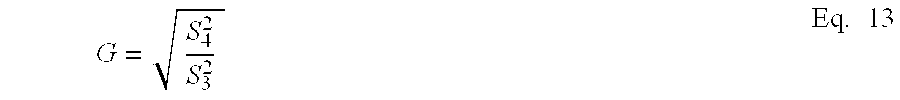
- a gain imbalance (G) can be determined as a function of the powers measured at 550 and 570 , such as indicated above in Eq. 13.
- a phase imbalance ( ⁇ ) is determined based on the measured powers P 1 and P 2 and the gain G determined at 580 .
- the phase imbalance or mismatch ( ⁇ ) thus can be computed based on the Eq. 10 indicated above. Accordingly, by using the gain and phase estimates determined at 580 and 590 , the I and Q signal components can be adjusted for each transmit signal to pre-correct or compensate for the relative gain and/or phase imbalances associated with the I and Q signal channels.
- FIG. 11 depicts a methodology that can be utilized to perform equalization correction in accordance with an aspect of the present invention.
- the methodology begins at 600 in which a signal (S i ) is generated for a selected one of a plurality of frequency tones in a given signal spectrum, where i denotes the selected tone.
- the power P i is measured for the signal generated at 600 .
- a reference measured power is determined for a selected one of the signals S i generated at 600 .
- the reference power P REF can correspond to a minimum power level detected at 610 for a corresponding one of the signals S i (e.g., a reference frequency tone).
- weight factors are computed for each of the other tones as a function of the reference power P REF .
- the weight factors for each of the frequency tones can provide an indication of the reference power P REF relative to the measured power P i for each of the other respective tones.
- the weight factor can correspond to a ratio of P REF and P i for each of the respective i tones (e.g., see Eq. 21).
- the weight factors can be computed to provide other spectral shapes.
- the weight factors can be stored for use during normal operation.
Abstract
Systems and methods are disclosed to improve a transmitter output signal. In one aspect, a correction system includes a power detector that provides an indication of power associated with a transmitter output signal. A compensation system employs the indication of power to compensate for at least one transmitter impairment affecting the transmitter output signal.
Description
- This patent application claims the benefit of U.S. Provisional Patent Application No. 60/468,753, which was filed May 7, 2003 and entitled WLAN Radio Transmitter Calibration Using A Transmit Power Detector, the entire contents of which is incorporated herein by reference.
- The present invention relates generally to communications devices and more particularly to systems and methods for correcting transmitter impairments.
- Wireless local area networks (WLANs) have been developed for various commercial and residential applications. Such networks allow for mobile terminals to be moved within a particular service area without regard to a physical connection to the network. To enable communications in the WLAN, various wireless standards have been developed, including the IEEE 802.11x standard, Blue Tooth, and hiperlan, to name a few. The architectural and operational parameters associated with these and other types of wireless communications systems can cause significant distortions in the signals. Both the radio transmitter and receiver can contribute to these distortions.
- Of particular interest are impairments in a WLAN system caused by a transmitter, including in-phase (I) and quadrature (Q) phase and amplitude imbalance, attenuation distortion in the transmit band and carrier level. Some possible sources of phase and gain mismatches in WLAN radios include differences in filter characteristics between the I and Q paths (e.g., due to semi-conductor process variations), which can result in both gain and phase imbalances that are generally frequency dependent. Additionally, differences in the I and Q path delays can cause phase imbalance that is proportional to frequency. A quadrature mixer that combines the I and Q components for transmission can also contribute to the total imbalance because of the gain and phase imbalance of the quadrature mixing signals.
- Many transmitter architectures employ multiple stages of filtering, each of which can contribute to amplitude distortion of the signal, such as due to ripple characteristics across the band for orthogonal frequency division multiplexing (OFDM) signals. The amplitude distortion may cause some OFDM tones to be attenuated several DB below other tones. This can result in a lower signal-to-noise ratio for the tones in the band thereby increasing the packet error rate. While the amplitude distortions in the OFDM tones can be equalized in the receiver, such equalization in the receiver also tends to enhance associated noise.
- An additional source of error in many WLAN architectures relates to an amplitude spike at the carrier frequency. For example, many transmitter implementations cause leakage at the center frequency component. WLAN standards specify requirements of the level for the center frequency component with respect to the overall power of the WLAN signal. Factory calibration typically is implemented to set the set of frequency components within the specified standard. However, the carrier level may change during operation due to changes in temperature or due to parts aging to the extent where the transmitter no longer meets the standard specifications.
- The present invention relates to systems and methods for correcting transmitter impairments. According to one embodiment of the present invention, a correction system includes a power detector that provides an indication of power associated with a transmitter output signal. A compensation system employs the indication of power to compensate for at least one transmitter impairment affecting the transmitter output signal. The transmitter impairment corrected by the compensation system can include, for example, spikes in a carrier signal, equalization errors, as well as gain and/or phase mismatch in in-phase and quadrature signal components. The correction system can be implemented as hardware, software or a combination of hardware and software.
- According to another embodiment of the present invention, a communications apparatus can include a baseband system that provides in-phase (I) and quadrature (Q) signal components. A correction system associated with the baseband system is operative to adjust at least one of the I and Q signal components based on an indication of power of a transmit signal to compensate for impairments associated with the communications apparatus. A power detector detects power provides the indication of power. A transmitter thus provides the transmit signal based on the adjusted I and Q signal components. As a result, the impairments are mitigated.
- Still another aspect of the present invention provides a method to correct impairments associated with a communications apparatus. The method includes detecting an indication of power associated with a transmit signal (e.g., by a power detector). An in-phase (I) signal component and/or a quadrature (Q) signal component is adjusted based on the indication of power to compensate for impairments associated with the communications apparatus that affect the transmit signal. The method can also implement calibration to set the adjustments to the I and/or Q signal components, which calibration can be implemented as an online or offline process.
- The foregoing and other aspects of the present invention will become apparent to those skilled in the art to which the present invention relates upon reading the following description with reference to the accompanying drawings.
- FIG. 1 depicts a transmitter system implementing a calibration system in accordance with an aspect of the present invention.
- FIG. 2 depicts an example of a transmitter configured to implement error correction in accordance with an aspect of the present invention.
- FIG. 3 depicts a block diagram of a carrier correction system in accordance with an aspect of the present invention.
- FIG. 4 depicts an example of a system for correcting I/Q mismatch errors.
- FIG. 5 depicts an example of an equalization system in accordance with an aspect of the present invention.
- FIG. 6 depicts an example of a sample transmit spectrum before equalization.
- FIG. 7 depicts a graph depicting a power detector response that can be utilized in accordance with an aspect of the present invention.
- FIG. 8 is a flow diagram illustrating a compensation method that can be implemented in accordance with an aspect of the present invention.
- FIG. 9 is a flow diagram depicting a methodology for implementing carrier correction in accordance with an aspect of the present invention.
- FIG. 10 is a flow diagram depicting a methodology for correcting I/Q mismatches in accordance with an aspect of the present invention.
- FIG. 11 is a flow diagram depicting a methodology for implementing equalization in accordance with an aspect of the present invention.
- FIG. 1 depicts an example of a
communications system 10 that can be implemented in accordance with an aspect of the present invention. Thesystem 10 can be implemented as a transmitter or a transceiver that includes atransmitter 12 configured to transmit awireless output signal 14. Abaseband system 16 provides in-phase (I) and quadrature (Q) signal components to the transmitter, based on which the transmitter provides thesignal 14. Acorrection system 18 is associated with thebaseband system 16 to correct for impairments in thesystem 10. The corrections can compensate for impairments associated with various aspects of system operation, such as by selectively adjusting characteristics of the I and/or Q signal components that are provided to thetransmitter 12. Thecorrection system 18 can be implemented as part of thebaseband system 16 or separate from the baseband system. - According to an aspect of the present invention, the
correction system 18 estimates correction based on a measure of energy in thetransmitter output signal 14. To measure the energy, thesystem 10 thus employs apower detector 20 that is coupled to detect the power associated with theoutput signal 14 provided by thetransmitter 12. Thepower detector 20 provides an indication of the output power to thebaseband system 16. Thecorrection system 18 employs the indication of output power provided by thepower detector 20 to implement the desired correction. Those skilled in the art will understand and appreciate various types of circuitry that can be utilized to detect power associated with theoutput signal 14. For example, many transmitter systems already implement power detectors utilized as feedback mechanisms for controlling the transmit power. Accordingly, thecorrection system 18 can leverage existing power detection circuitry. - By way of further example, the
correction system 18 can be configured during a calibration mode. The calibration mode can involve one or more calibration phases based on the number and type of impairments to be corrected. For instance, the correction system can be programmed in a first phase to correct for spikes in the carrier level, in a second phase to correct for I/Q mismatches and in a third phase to equalize the signal spectrum. - By amplifying the output of the power detector 20 (the indication of power) sufficiently, the power level of individual tones or sets of tones provided by the
baseband system 16 can be measured to estimate impairments in thetransmitter system 10. To facilitate implementing desired correction for thesystem 10, the corrections can be implemented based on relative measurements within the system, such as by employing power ratios (e.g., between the respective I and Q signal components) rather than based on the absolute detected power levels. Thus, thecorrection system 18 can utilize the estimated impairment to selectively adjust the I and Q signal components to correct for such impairments without requiring calibration of the power detector. - As an example, the
correction system 18 can be adapted to correct for spikes in the carrier signal. Spikes in the carrier signal can be mitigated by selectively adjusting DC levels of one or both of the I and Q signal components based on the indication of power provided by thepower detector 20. This can be implemented during a first calibration mode in which data and other information has been removed from the I and Q signal components provided to thetransmitter 12. Thecorrection module 18 can then adjust the DC level of the I and Q signal components until a desired signal level is achieved for the carrier. - Additionally, the
correction system 18 can correct for I/Q mismatches in thetransmitter system 10. The I/Q mismatches, for example, can correspond to phase and gain mismatches due to variations between the signal paths associated with the respective I and Q signal components. These mismatches can corrupt the transmitted signal thereby increasing the bit error rate when the signal is finally demodulated at a receiver (not shown). In addition, phase and gain imbalances in the quadrature mixer of the radio device can combine with the signal path differences to further exacerbate the degradation. One possible source of the mismatch include semiconductor process variations, which can result in both gain and phase imbalances that are generally frequency dependent. Additionally, differences in the I and Q path delays can impose a phase imbalance generally proportional to frequency. A quadrature mixer in thetransmitter 12 can further contribute to the total imbalance because of gain and phase imbalances of the quadrature mixing signals. - Thus, to compensate for the I/Q mismatches, the
correction system 18 can employ thepower detector 20 to measure the power associated with each of the I and Q signal components. For example, thecorrection system 18 can independently control the relative magnitude and sign of the respective I and Q signal components over a plurality of signals. The corresponding measure of power provided by thepower detector 20 can in turn be utilized to ascertain both the phase imbalance and the gain mismatch associated with the respective I and Q signal components. - The
correction system 18 can also compensate for attenuation distortion associated within the signal spectrum or band. For example, thecorrection system 18 can control thebaseband system 16 to provide desired calibration tones, with thepower detector 20 measuring corresponding power for each tone. Thecorrection system 18 can compute factors or weights to pre-correct the transmit tone levels based on the indication of power provided by the power detector for each individual tone. For example, a reference tone (e.g., corresponding to one of the calibration tones) can be utilized as a basis to which all the other tones are corrected by applying suitable weighting parameters to adjust their respective power levels. Thecorrection system 18 thus can employ the weight factors to achieve a desired shape for the signal spectrum (e.g., equalization). - It is to be understood and appreciated that the
transmitter system 10 can be configured to implement any one or more of the modes of correction described herein. The calibration of thetransmitter system 10 can be implemented by thecorrection system 18 at power up and/or intermittently during normal operation to achieve desired performance. - FIG. 2 depicts an example of a communication system (e.g., a transmitter portion) 50 that can be implemented in accordance with an aspect of the present invention. The
system 50 includes acontrol system 52 that is programmed and/or configured to implement desired correction to improve operation of thesystem 50. In particular, thecontrol system 52 includes acorrection component 54 that is operative to calibrate characteristics of thecommunication system 50 based on an output power level, namely a transmit power. Thecontrol system 52 employs thecorrection component 54 to provide compensated quadrature baseband input signals, namely an in-phase (I) signal component and a quadrature (Q) signal component. As described herein, thecorrection component 54 is operative to mitigate errors or impairments by implementing desired compensation on one or both of the I and Q components. - According to an aspect of the present invention, the
correction component 54 can include acarrier correction component 56, an I/Q gain and/orphase correction component 58 and anequalization component 60. It will be understood and appreciated that improved performance can be achieved by utilizing one or any combination of such correction components 56-60. - The
communications system 50 includesseparate paths control system 52 provides the I signal component to a baseband filter block (HI) 66, which can include one or more filters. Thebaseband filter block 66 is configured to provide a desired frequency response for the I-signal component. Thebaseband filter block 66 provides a corresponding output signal to anamplifier 68 having a gain (Gi) that amplifies the signal to a desired level. The amplified output signal is provided to amixer 70. Themixer 70 mixes the output signal from theamplifier 68 with a signal provided by alocal oscillator 72. Themixer 70 thus combines the amplified output signal with the carrier provided by thelocal oscillator 72 to produce corresponding I signal component for the I-signal path 62. - With regard to the
Q signal path 64, thecontrol system 52 provides the Q signal component to a baseband filter block 74 (HQ) (e.g., one or more filters) that implements a desired frequency response on the Q signal component. Thebaseband filter block 74 provides a corresponding output signal to anamplifier 76 having a gain (GQ) that amplifies the filtered Q signal component to a desired level. Theamplifier 76 provides the amplified signal to amixer 78, which combines the amplified signal with a phase shifted carrier signal. In this example, thelocal oscillator 72 provides the carrier signal to a quadraturephase shift component 80 that provides a phase shifted carrier signal to themixer 78. The mixer provides the Q signal component at a desired frequency (e.g., an intermediate frequency) to acombiner 82. - The
combiner 82 combines the I and Q signal components and provides the aggregate signal to avariable gain amplifier 84. Thecontrol system 52 can provide a control signal to theamplifier 84 to selectively set the gain of the amplifier. Theamplifier 84 provides an amplified aggregate signal to anothermixer 86 that combines the aggregate amplified signal with a desired carrier frequency provided by a radio frequency (RF)synthesis component 88. Themixer 86 produces a signal having a desired transmission frequency that is provided to afilter 90. Thefilter 90 implements a transfer function (e.g., a bandpass filter) to achieve a desired frequency response. Thefilter 90 provides a filtered output signal to an associated power amplifier (PA) 92. Thepower amplifier 92 provides the corresponding amplified output signal to anantenna 94 through a directional coupler (DC) 96. Thepower amplifier 92 is configured to amplify the filtered signal to a desired level for transmission. - A
power detector 98 is operatively coupled to thedirectional coupler 96 to detect transmission power. Thepower detector 98 provides a power detection signal to thecontrol system 52 indicative of a measure of energy associated with the transmit signal. By way of example, thepower detector 98 can be implemented by circuitry implementing a squaring function (or an absolute value function) 100 that is provided to alow pass filter 102 to remove high frequency signal components from the signal. - The
control system 52 employs the measure of energy provided by thepower detector 98 to implement appropriate compensation and calibration of one or more transmitter impairments associated with distortion in the output signal. As mentioned above, the compensation implemented by thecorrection module 54 can correct for one or more of carrier spikes, I/Q gain and/or phase mismatches as well as adjust the spectral shape of the transmit output signal. - For example, the
carrier correction component 56 can be programmed or configured during a calibration mode for each of the I and Q signal components. For instance, a test signal having no information (e.g., only DC signals) can be provided to theI signal path 62 while no signal is provided to theQ signal path 64. Thecarrier correction component 56 can optimize the I signal component based on the measure of energy provided by thepower detector 98. After a desired power level is achieved for the I signal component, thecarrier correction component 56 can apply a DC signal to the Qsignal component path 64, while no signal is provided to theI signal path 62. Thecarrier correction component 56 can then implement desired compensation/optimization for theQ signal path 64 based on the measure of power indicated by the signal provided by thepower detector 98. - The I/
Q correction component 58 can correct one or both I/Q gain and phase mismatch based on an indication of the I/Q mismatch determined during an associated calibration process. The calibration process can include providing suitable calibration tones to the I and/orQ signal paths Q correction component 58 can estimate gain and phase mismatch based on the power detection signal provided by thepower detector 98 for respective calibration tones for each of the I andQ signal paths Q correction component 58 can modify the respective I and Q signal components during normal operation to compensate for the mismatches determined during calibration. As a result, the transmit signals can be dynamically adjusted during normal operation to compensate for imbalances in the gain and phase associated with therespective signal paths - The
equalization correction component 60 employs a series of calibration tones for a given frequency spectrum (or band) to ascertain an appropriate level of correction for each tone in the frequency band based on power detector measurements for each tone. Theequalization correction component 60 determines a weighting factor to apply to the respective tones to compensate for signal attenuation across the frequency spectrum, thereby equalizing the transmit levels relative to that of a reference tone selected during calibration. During normal operation, theequalization component 60 applies pre-correction to the transmit tone levels, such that the frequency band or spectrum can maintain an improved equalization across the band. - The
correction system 54 also can include abias correction component 61 programmed and/or configured to compensate for DC bias associated with thepower detector 98. Thebias correction component 61, for example, determines a value indicative of DC bias associated with operation of thepower detector 98. Theequalization component 60 and the I/Q correction component 58 can, in turn, employ the detector bias value when performing corresponding compensation implemented by such components. That is, thesecomponents - Where the
correction system 54 is implemented to includecarrier correction component 56, I/Q correction component 58 andequalization correction component 60, it is desirable to calibrate thecorrection system 54 for carrier level first, for I/Q mismatch next and for equalization after carrier level and I/Q mismatch calibration. This approach mitigates the impact that each of the previously corrected impairments may have on the subsequently calibrated features. - Those skilled in the art will appreciate various types of transmitter architectures that can implement correction based on the teachings contained herein. For example, not all transmitter designs may require implementing each of the modes of compensation, including carrier suppression, I/Q mismatch correction, and equalization. Accordingly, those skilled in the art will understand how to implement appropriate aspects of correction as well as how to implement calibration thereof based on the teachings contained herein.
- By way of further example, FIG. 3 depicts an example of a
carrier correction system 150 that can be implemented in accordance with an aspect of the present invention. Thecarrier correction system 150 includes asignal generator 152 that is operative to provide I and Q signal components. In particular, thesignal generator 152 includes a DCI block 154 that is operative to provide a DC bias to the I-signal path and a DCQ block 156 that is operative to provide a DC bias to the Q signal path. A carrier offsetcorrection module 158 controls the DCI and DCQ blocks 154 and 156, respectively. - The carrier offset
correction module 158 can perform optimization for the I and Q channels to compensate for low frequency leakage associated with the transmitter to which the I and Q signal components are provided. The carrier offsetcorrection module 158 implements the adjustments to the I and Q signal based on a measure of energy associated with a transmit power based on the I and Q signal components provided by thesignal generator 152, such as determined during a calibration mode. Thecarrier correction system 150 receives a POWER signal indicative of a measure of transmitter carrier energy, such as from a power detector (see, e.g., FIG. 2). An analog-to-digital converter 160 converts the POWER signal to a digital representation thereof. Apower measurement component 162 determines an indication of measured power based on the digital representation of power provided by the A/D converter 160. The power measurement component provides the indication of power to the carrier offsetcorrection module 158. The carrier offsetcorrection module 158 in turn employs the calculated power to control the DC offset for each of the I and Q signal paths. - By way of example, the carrier offset
correction module 158 adjusts the DC bias for the I-signal path to achieve a desired power level while no signal is provided to the Q signal path. After achieving a desired power level with the I-signal path, the carrier offsetcorrection module 158 selectively adjusts the DC bias for the Q signal by adjusting the DC bias for the I-signal path (DCI) and the DC bias signal for the Q signal path (DCQ). Thus, thesignal generator 152 employs the DCI and DCQ blocks 154 and 156 to provide signals without energy in the in-band frequencies, such that only the carrier frequency remains. The carrier offsetcorrection module 158 can ascertain a set of DC inputs that minimizes the carrier component in the transmission signal based on the calculated power provided by thepower measurement component 162 for each of the adjusted DC bias levels. - By way of further example, in transmitter devices that employ DC coupling to the baseband inputs, carrier offset can be controlled by adjusting complex I and Q signal components, indicated at I T and QT. For instance, by setting IT=DCI and QT=DCQ, the signal S(t) provided (e.g., by a power amplifier to a power detector) can be represented as:
- S(t)∝DC I cos(ωc t+φ)−DC Q sin(ωc t+φ) Eq. 1
- where ω c corresponds to the carrier frequency, and
- φ denotes an arbitrary phase of the transmit signal.
- From Eq. 1, it will be appreciated that a set of DC inputs can be determined to minimize the carrier component in the transmit signal. The set of DC inputs can be determined, for example, by the carrier offset
correction module 158 selectively adjusting DCI and DCQ while measuring an indication of the power (e.g., corresponding to the carrier level) with the power detector for each adjustment. As a result, a desired set of DC inputs can be determined to configure DC inputs that provide a minimum carrier level during normal operation. - Those skilled in the art will appreciate various optimization algorithms that can be utilized to determine suitable DC bias levels for the respective I and Q signal components to mitigate the carrier spikes that might otherwise occur. Since erroneous energy in the carrier might corrupt measurements associated with the I/Q signal phases, it is desirable to calibrate the
carrier correction system 150 prior to calibrating for I/Q gain and phase mismatches, as described herein. - FIG. 4 depicts an example of an I/Q
mismatch correction system 200. Thesystem 200 is programmed and/or configured to ascertain an indication of gain and phase mismatch for I and Q signal paths of an associated transmitter. The mismatches between the I and Q signal components, for example, can be associated with different filter characteristics in the I and Q signal paths, such as may be due to semiconductor process variations. Additionally, there can be different path delays associated with the I and Q signal paths that can cause further imbalances which may be proportional to frequency. A quadrature mixer employed by transmitter circuitry further can contribute to the total imbalance of the gain and phase of the mixing between the signals. - The
system 200 receives a POWER signal indicative of a measure of energy associated with a transmit signal based on I and/or Q signal components provided by thesystem 200. Thesystem 200 includes asignal generator 202 that includessignal generator block 204 for the I-signal path and asignal generator block 206 for the Q signal path. An I/Q phase control 208 is operative to control the signal generator blocks 204 and 206 to achieve desired calibration to mitigate impairments, such as due to gain and phase mismatches. The I/Q phase control 208 ascertains gain and phase mismatches, for example, based on measures of energy provided by a power detector in conjunction with selected signals provided to the transmitter on the I and Q signal paths during an I/Q calibration mode. - During the calibration mode, for example, an A/
D converter 209 provides a digital indication of power to apower measurement component 210. Themeasurement component 210 determines an indication of power for the respective calibration tones provided by the signal generator for each of the I and Q signal paths. By independently applying each calibration tone to each of the I and Q signal paths, a measure of power can be obtained separately for the I-signal path and for the Q signal path. Thepower measurement component 210 can also receive a detector bias signal corresponding to DC bias associated with operation of a power detector that provides the power signal. The power measurement component thus can employ the detector bias signal to compensate for detector bias when computing the indication of power. The respective power measurements for the I and Q signal paths can be stored inmemory 212. For example, thememory 212 includes registers orother storage devices comparator 218 compares the stored I power and Q power measurements to ascertain a mismatch between the power levels for a given calibration tone. Thecomparator 218 provides a comparator output signal to the I/Q phase control 208 that can implement further adjustments to the I and Q signal components based on the comparator output signal. - The I/
Q phase control 208 can be programmed to implement an algorithm to ascertain gain and phase mismatches between the I and Q signal components. For instance, regardless of what components of the transmitter contribute to phase and/or gain mismatch, the mismatch can be modeled at any particular frequency as a distortion of the baseband input signal components IT and QT, which are provided by thesignal generator 202. - By way of example and with reference back to FIG. 2, the baseband I T signal component can be represented as:

- and the baseband Q T signal component can be represented as:

- where G and Δ are the gain and phase imbalances, respectively. In the second set of Eqs. 2 and 3, a small angle approximation (i.e., cos(Δ/2)≈1, sin(Δ/2)≈

- is utilized to provide a shorthand representation for I T and QT. By mixing these signals (IT and QT) to passband, the output S(t) of a power amplifier can be represented as:

- In Eq. 4, A represents any gain added after the quadrature mixer and ω c is the carrier frequency. Eq. 4 can be considered an indication the output power of an ideal transmitter with distorted inputs I′T and Q′T, which can be re-presented as:
- S(t)=AI′ T cos(ωc t)−AQ′ T sin(ωc t) Eq. 5
- The magnitude squared of the transmit signal is the sum of the squares of the components. Accordingly, at the output of the power detector (e.g., 98 in FIG. 2) after low pass filtering, the power measurement provided by the power detector reduces to:

- Assuming that Δ 2/4 is much less than 1, the terms proportional to Δ2/4 can be dropped to provide that:

- In Eq. 7, if the sign of either I T or QT is changed, the magnitude of the transmitted signal decreases. Accordingly, by selecting the transmit signals appropriately, the I/
Q phase control 208 can estimate phase and gain imbalances by measuring the magnitudes of the respective signals at the output of the power detector. - By way of further example, if the same baseband signal is applied to both the I T and QT signal components at the input to the radio transmitter (e.g., IT=QT=Ψ), then, from Eq. 7, the square magnitude of the vector at the output of the power detector (S1) becomes:

- Similarly, by changing the sign of the signal on either the I or Q rail (e.g., I T=−Ψ, QT=Ψ) the output of the power detector (S2) can be expressed as:

- Solving Eqs. 8 and 9 for the phase imbalance Δ yields:

- The gain imbalance G can be determined by generating two additional power detector signals S 3 and S4 associated with transmitter inputs IT=Ψ, QT=0 and IT=0, QT=Ψ, respectively. The square magnitude of the signals generated from these inputs can be expressed as:

- Eqs. 11 and 12 can be solved for G to provide:
- From the foregoing, it will be appreciated that the phase imbalance and the gain imbalance can be computed during calibration of the I/
Q correction system 200 for different frequencies. The I/Q phase control 208 can thus adjust the respective I and Q signal components to compensate for the computed mismatch at each of the respective frequencies. - FIG. 5 depicts an example of an
equalization system 250 that can be implemented in accordance of an aspect of the present invention. Thesystem 250 can mitigate attenuation across a given frequency band as tends to occur due to filtering at baseband, at the intermediate frequency as well as at RF prior to the signal being sent to the antenna for transmission. In the example of FIG. 5, thesystem 250 includes asignal generator 252 that provides I and Q signal components at baseband. Acontrol 254 is operative to control each of the I and Q signal components based on calibration performed for each of a plurality of tones in a given frequency band. The following example assumes the signal provided by combining the I and Q signal components corresponds to an orthogonal frequency division multiplexing (OFDM) signal, although it is to be understood and appreciated that theequalization system 250 is equally applicable to other types of modulation. - By way of example, the
control 254 controls thesignal generator 252 to provide I and Q signal components for each respective tone, there being 52 OFDM tones in an OFDM signal. Thesystem 250 receives an analog indication of POWER (e.g., from a transmit power detector) for each OFDM tone during a calibration phase. The analog indication of POWER is converted to a digital representation thereof by an A/D converter 256. - A
power measurement component 258 computes a relative power for a given respective tone based on the digital representation thereof provided by the A/D converter 256. Thepower measurement component 258 can also receive a detector bias signal indicative of a bias associated with operation of a power detector (not shown), which is coupled to measure the transmit power at the output of the power amplifier. Thepower measurement component 258 thus can employ the detector bias signal to compensate power measurements for the bias associated with the power detector (e.g., subtracting out the bias from the indication of power) and thereby enable improved equalization correction by thesystem 250. Thepower measurement component 258 also provides the indication of power to apower data module 262. - The
power data module 262 is operative to store the computed power as power values for each respective tone (e.g., indicated at P1 through Pn). Thepower data module 262 can also employ asmoothing block 263 to remove possible standing wave ripple components perceived by the power detector (e.g., on the line between thepower amplifier 92 and theantenna 94 of FIG. 2). Those skilled in the art will understand and appreciate various approaches (e.g., hardware and/or software algorithms) that can be implemented to achieve suitable smoothing of the transmit signal monitored by the power detector. For example, the smoothing block can be implemented in software as a filter. By mitigating the effects of the detector bias and implementing desired smoothing to reduce ripple effects, the power measurements P1 through Pn can correspond to raw power values associated with respective tones, less any bias added by the power detector. - A reference power value P ref is obtained from the measured power values P1 through Pn corresponding to the power measurement for a reference tone. The reference power Pref is utilized as a basis for a reference tone that provides a desired output power level to which the other reference tones are calibrated. For example, the reference power value Pref can correspond to the tone determined to have the lowest associated transmit energy level from the set of calibration tones.
- A
calibration system 264 employs the power data from thepower data module 262 to calibrate the power levels for each respective tone 1-n relative to the reference power value Pref. For example, thecalibration system 264 includes acomparator 266 that compares the indication of power associated with each tone P1 through Pn with Pref. Aweighting component 268 computes weighting factors that are to be applied to each tone to pre-weight the power so that the power level for each respective tone matches that of the reference tone indicated by Pref. The pre-weight factors are stored aspower control data 270. The power control data associates weighting factors W1 through Wn with the respective frequencies f1 through fn for the n OFDM tones in the signal spectrum. - After the pre-weight factors W 1 through Wn have been computed by the
weighting function 268, thecontrol 254 can employ the pre-weight factors W1 through Wn to perform an equalization function so that the power levels for each of the respective frequencies f1 through fn in the signal spectrum are substantially equalized relative to the reference tone. - By way of further example, FIG. 6 depicts an example of transmit
signal spectrum 280 prior to employing theequalization system 250. In order to demonstrate one approach that can be utilized to implement desired equalization, assume twotest tones signal generator 252 with equal amplitudes α0. - FIG. 7 illustrates a square law response, indicated at 292 and 294, for the power associated with each of the
respective tones - P 1=λ1α0 2 Eq. 14
- P 2=λ2α0 2 Eq. 15
- A correction factor f that can be applied to equalize the two tones at the output of the transmitter (wherein
tone 284 is utilized as the reference tone) can be expressed as:
- Thus,
tone 282 can be equalized to the level oftone 284 at the output of the power amplifier by multiplying the baseband inputs IT1 and QT1 by the correction factor f. For example, baseband inputs IT1 and QT1 fortone 282 can be represented as: - I T1(t)=fα 0 cos(ωt) Eq. 17
- Q T1(t)=fα 0 sin(ωt) Eq. 18
- and for
tone 284 as: - I T2=α0 cos(ωt) Eq. 19
- Q T2=α0 sin(ωt) Eq. 20
- From the foregoing two-tone example, those skilled in the art will understand and appreciate that a similar approach can be employed to equalize any set of two or more tones, such as the set of OFDM tones that comprise an entire transmit bandwidth. Any one (or more) tones thus can be selected as the reference tone and appropriate correction factors can be computed (e.g., by the weighting function 268). For example, to achieve a substantially equalized spectrum, a correction factor fi can be computed for each tone, as follows:

- While the above example describes an approach to achieve a substantially equalized spectrum, the approach can be extended to achieve any desired spectral shape. For example, a particular spectral profile may be determined to be more beneficial in certain circumstances than a flat response. Additionally, after equalizing the individual tones to a desired reference power level, it may be necessary to scale the entire transmit signal to maintain a suitable transmit level.
- In view of the foregoing structural and functional features described above, certain methodologies that can be implemented will be better appreciated with reference to FIGS. 8-11. While, for purposes of simplicity of explanation, the methodologies of FIGS. 8-11 are shown and described as being implemented serially, it is to be understood and appreciated that the illustrated actions, in other embodiments, may occur in different orders and/or concurrently with other actions. Moreover, not all illustrated features may be required to implement a method according to an aspect of the present invention. It is to be further understood that the following methodology can be implemented in hardware, such as one or more integrated circuits, software, or any combination of hardware and software.
- FIG. 8 depicts a methodology that can be utilized to compensate for impairments in a communications system. In one particular aspect, the methodology can be utilized at a transmitter to reduce transmitter impairments associated with, for example, I/Q phase and amplitude imbalance, attenuation distortion in the transmit band and distortion (e.g., spikes) in the carrier level. The methodology can be implemented during a calibration mode (e.g., off line) as well as during normal operation. The methodology begins at 300 in which a transmit power is detected. The transmit power provides an indication of the measured energy associated with a signal spectrum and/or individual tones in the signal spectrum.
- At 310, carrier correction is implemented. The carrier correction can be implemented based on the detected power at 300 for a transmit signal containing no data (e.g., carrier only). The carrier correction can be implemented by adjusting the DC levels of I and Q signal components so as to minimize the carrier level in the transmit signal, such as to a level generally commensurate with the level of the tones in the signal spectrum.
- At 320, I/Q mismatch correction is performed. The I/Q signal component mismatch can be implemented by measuring the power at 300 associated with calibration tones provided separately for respective I and Q signal components. Based on the measured energy levels for the respective I and Q signal components for various calibration tones, gain and phase mismatch associated with the respective I and Q channels (e.g., represented as a ratio between the respective I and Q channel) can be ascertained. The detected mismatch can then be utilized to provide compensation signals for each of the respective I and Q components during the normal operating mode.
- At 330, equalization correction is performed. The equalization correction can be implemented based on the detected power at 300 for each of the plurality of tones (or at least a selected subset thereof), for a given signal spectrum. Power associated with each of the tones can be compared to a measured power value for a selected reference tone and the other tones can then be weighted accordingly to provide a desired spectral (e.g., an equalized or curved) shape across the signal spectrum.
- It is to be appreciated that additional benefits can be utilized by performing the compensation with carrier correction ( 310) first, I/Q mismatch correction (320) next and equalization (330) thereafter. This is because energy in the carrier can further affect the measurements associated with the I/Q phase mismatch. Additionally, the I/Q phase mismatch can extend into the equalization. Thus, by performing the different phase of correction in order can further improve transmitter performance. Those skilled in the art will appreciate that the compensation can also be performed in different orders from that described herein.
- FIG. 9 depicts an example of a methodology that can be utilized to implement carrier correction in accordance with an aspect of the present invention. The methodology begins at 400 in which DC signals are generated for I and Q components, indicated at DCI and DCQ. At 410, output power is measured for the transmit signal based on the DCI and DCQ signal components generated at 400.
- At 420, a determination is made as to whether the output power is within expected parameters. If the output power is not within expected parameters (NO), the methodology proceeds to 430. At 430, the DCI and DCQ signal components are adjusted and the methodology returns to 400 in which the adjusted DC levels are utilized to generate additional DC signals for the I and Q signal components. If the output power at 420 is within expected operating parameters (YES), the methodology proceeds to 440 in which the DC offset components are calibrated for the I and Q signal components. The calibrated DCI and DCQ signal components can be utilized during normal operation to mitigate carrier spikes that can be associated with the transmit signal.
- FIG. 10 depicts a methodology that can be utilized for I and Q compensation in accordance with an aspect of the present invention. The methodology begins at 500 in which transmit signal S1 is generated, such as at baseband in which I and Q signal components are substantially equal (e.g., IT=QT=Ψ). At 510, a corresponding power P1 is measured at 510 based on the generated transmit component associated with the S1 signal. The measured power P1 can be stored for subsequent calculations. At 520, a transmit signal is generated, such as at baseband in which I and Q-signal components are substantially equal in magnitude, but have opposite signs (IT=QT=−Ψ), and a corresponding power P2 is measured at 530. The measured power P2 corresponds to the transmit signal S2.
- At 540, an additional transmit signal S3 is generated, such as based on a baseband inputs for an I-signal component having a desired magnitude (e.g., IT=Ψ and QT=0). Associated power P3 is measured at 550 for the signal generated at 540. At 560, another signal S4 is generated, such as in which QT=Ψ and the in-phase signal component 0IT==0. The power of P4 is measured at 570 for the signal S4 generated at 560. At 580, a gain imbalance (G) can be determined as a function of the powers measured at 550 and 570, such as indicated above in Eq. 13. At 590, a phase imbalance (Δ) is determined based on the measured powers P1 and P2 and the gain G determined at 580. The phase imbalance or mismatch (Δ) thus can be computed based on the Eq. 10 indicated above. Accordingly, by using the gain and phase estimates determined at 580 and 590, the I and Q signal components can be adjusted for each transmit signal to pre-correct or compensate for the relative gain and/or phase imbalances associated with the I and Q signal channels.
- FIG. 11 depicts a methodology that can be utilized to perform equalization correction in accordance with an aspect of the present invention. The methodology begins at 600 in which a signal (Si) is generated for a selected one of a plurality of frequency tones in a given signal spectrum, where i denotes the selected tone. At 610, the power Pi is measured for the signal generated at 600. At 620, a determination is made as to whether power has been measured for each of the plurality of signal tones in the spectrum. If additional tones exist (NO), the methodology proceeds to 630 in which the signal Si is incremented (i=i+1) to provide a next signal tone. The methodology then returns to 600. After signals Si have been generated at 600 and power has been measured at 610 for each of the plurality of tones (YES), the methodology proceeds from 620 to 640. At 640, a reference measured power (PREF) is determined for a selected one of the signals Si generated at 600. The reference power PREF, for example, can correspond to a minimum power level detected at 610 for a corresponding one of the signals Si (e.g., a reference frequency tone).
- At 650, weight factors are computed for each of the other tones as a function of the reference power PREF. The weight factors for each of the frequency tones can provide an indication of the reference power PREF relative to the measured power Pi for each of the other respective tones. For example, the weight factor can correspond to a ratio of PREF and Pi for each of the respective i tones (e.g., see Eq. 21). Thus, by multiplying the weight factor by the power levels for a given tone, such as during normal operation, the signal spectrum can be substantially equalized to substantially the same the level as the reference tone. Those skilled in the art will appreciate that different weight factors can be computed to provide other spectral shapes. At 660, the weight factors can be stored for use during normal operation.
- What has been described above includes examples and implementations of the present invention. Because it is not possible to describe every conceivable combination of components, circuitry or methodologies for purposes of describing the present invention, one of ordinary skill in the art will recognize that many further combinations and permutations of the present invention are possible. Accordingly, the present invention is intended to embrace all such alterations, modifications and variations that fall within the spirit and scope of the appended claims.
Claims (33)
1. A correction system comprising:
a power detector that provides an indication of power associated with a transmitter output signal; and
a compensation system that employs the indication of power to compensate for at least one transmitter impairment affecting the transmitter output signal.
2. The system of claim 1 , the compensation system being configured to selectively adjust at least one of an in-phase (I) signal component and a quadrature (Q) signal component based on the indication of power to mitigate distortion characteristics in the transmitter output signal.
3. The system of claim 2 , the indication of power further comprising a relative power measured by the power detector associated with the respective I and Q signal components.
4. The system of claim 1 , the compensation system further comprising a carrier correction system that adjusts DC offset of at least one of an in-phase (I) signal component and a quadrature (Q) signal component utilized to provide the transmitter output signal based on the indication of power to mitigate spikes in the carrier level of the transmitter output signal.
5. The system of claim 1 , the compensation system further comprising an equalization system that adjusts tones in a signal spectrum employed to provide the transmitter output signal so that the signal spectrum has a desired spectral shape, the equalization system adjusting the tones in the signal spectrum during calibration based on the indication of power.
6. The system of claim 5 , the equalization system selectively weighting tones in the signal spectrum based on an indication of power associated with the tones in the signal spectrum relative to an indication of power associated with a reference tone in the signal spectrum.
7. The system of claim 6 , further comprising:
a comparator that compares a power characteristic associated with each of the tones in the signal spectrum relative to a power characteristic of the reference tone to provide an indication of relative power for each respective tone; and
a weighting function that employs the indication of relative power for each respective tone to adjust each respective tone to a desired level relative to the reference tone.
8. The system of claim 7 , the weighting function being applied to adjust at least one of the I-signal component and the Q-signal component of the transmitter output signal to provide the desired spectral shape.
9. The system of claim 1 , further comprising a detector bias component configured to determine a DC bias associated with operation of the power detector, the compensation system employing the DC bias to mitigate effects of the DC bias in the indication of power.
10. The system of claim 1 , the compensation system is operative to adjust at least one of an in-phase (I) signal component and a quadrature (Q) signal component based on the indication of power to compensate for at least one of a gain and phase mismatch between a signal path for the I-signal component and a signal path for the Q-signal component.
11. The system of claim 1 , further comprising a mismatch correction system operative to ascertain an indication of at least one of a gain and phase mismatch between an in-phase (I) signal component and a quadrature (Q) signal component based on the indication of power, the mismatch correction system adjusting at least one of the I-signal component and the Q-signal component based on the indication of the mismatch between I and Q signal components.
12. The system of claim 11 , the mismatch correction system further comprising:
a comparator that compares the indication of power associated with the I-signal component and the indication of power associated with Q-signal component to provide an indication of relative power characteristics corresponding to the mismatch associated with a signal path for the I-signal component and a signal path for the Q-signal component; and
a control operative to adjust at least one of the I and Q signal components based on the indication of the relative power characteristics.
13. An integrated circuit comprising the system of claim 1 .
14. A communications apparatus comprising:
a baseband system that provides in-phase (I) and quadrature (Q) signal components;
a correction system associated with the baseband system for adjusting at least one of the I and Q signal components based on an indication of power of a transmit signal to compensate for impairments associated with the communications apparatus;
a transmitter that provides the transmit signal based on the adjusted I and Q signal components; and
a power detector that detects power associated with the transmit signal and provides the indication of power.
15. The apparatus of claim 14 , the correction system further comprising a carrier correction system that adjusts a level of at least one of the I and Q signal components based on the indication of power to compensate for an impairment associated with the communications apparatus that affects a level of the carrier signal in the transmit signal.
16. The apparatus of claim 15 , the correction system further comprising an equalization system that adjusts tones in a signal spectrum corresponding to the transmit signal based on the indication of power so that the signal spectrum has a desired spectral shape.
17. The apparatus of claim 16 , the equalization system selectively weighting tones in the signal spectrum based on an indication of power associated with the tones in the signal spectrum relative to the indication of power associated with a reference tone in the signal spectrum.
18. The apparatus of claim 16 , the correction system further comprising a mismatch correction system operative to ascertain, based on the indication of power, an indication of mismatch associated with a signal path for the I-signal component and a signal path for the Q-signal component, the mismatch correction system adjusting at least one of the I-signal component and the Q-signal component based on the indication of the mismatch between I and Q signal components.
19. The apparatus of claim 18 , wherein the mismatch further comprises at least one of a phase imbalance and a gain mismatch caused by circuitry in the signal path for the I-signal component and the signal path for the Q-signal component.
20. An integrated circuit comprising the system of claim 14 .
21. A transmitter system comprising:
means for determining an indication of power associated with a transmit output signal; and
means for compensating for distortion in the transmit output signal based on the indication of power.
22. The system of claim 21 , further comprising means for shaping a signal spectrum in the transmit output signal by adjusting at least one of an in-phase (I) signal component and a quadrature (Q) signal component based on the indication of power.
23. The system of claim 21 , further comprising means for, based on the indication of power, compensating for at least one of gain and phase mismatch associated with an in-phase signal path and a quadrature signal path of the transmitter system.
24. The system of claim 21 , further comprising means for mitigating spikes in a carrier signal of the transmit signal by applying a DC signal to, based on the indication of power, adjust at least one of an in-phase (I) signal component and a quadrature (Q) signal component.
25. The system of claim 21 , wherein the impairments comprise at least one of spikes in a carrier signal of the transmit signal, attenuation distortion in a signal spectrum corresponding to at least a portion of the transmit signal, a gain mismatch associated with an in-phase (I) signal path and a quadrature (Q) signal path, and a phase mismatch associated with the I-signal path and the Q-signal-path.
26. The system of claim 25 , further comprising means for calibrating the means for compensating to mitigate the impairments.
27. The system of claim 26 , the means for calibrating further comprising:
means for providing at least one calibration tone having an I-signal component and a Q-signal component; and
means for adjusting at least one of the I-signal component and the Q-signal component based on the indication power, the means for compensating employing the adjusted at least one of the I-signal component and the Q-signal component to mitigate the impairments.
28. A method to correct impairments associated with a communications apparatus, the method comprising:
detecting an indication of power associated with a transmit signal; and
selectively adjusting at least one of an in-phase (I) signal component and a quadrature (Q) signal component based on the indication of power to compensate for impairments associated with the communications apparatus that affect the transmit signal.
29. The method of claim 28 , further comprising applying a DC offset for at least one of the I-signal component and the Q-signal component to mitigate spikes in a carrier for the transmit signal.
30. The method of claim 28 , further comprising adjusting at least one of the I-signal component and the Q-signal component based on the indication of power to mitigate at least one of gain and phase mismatches associated with an I-signal path and a Q-signal path to which the respective I-signal component and the Q signal component are provided.
31. The method of claim 30 , further comprising:
determining an indication of a phase imbalance associated with the I-signal path and the Q-signal path;
determining an indication of a gain mismatch associated with the I-signal path and the Q-signal path; and
calibrating the adjustments to the at least one of the I-signal component and the Q-signal component based on the indication of the phase imbalance and the indication of the gain mismatch.
32. The method of claim 28 , further comprising applying weight factors to at least one of the I-signal component and the Q-signal component for tones that form a signal spectrum of the transmit signal for adjusting a spectral shape of the transmit signal.
33. The method of claim 32 , further comprising determining a weight factor for each of the tones based on an indication of power associated with each respective one of the tones relative to an indication of power associated with a reference one of the tones.
Priority Applications (1)
| Application Number | Priority Date | Filing Date | Title |
|---|---|---|---|
| US10/790,525 US20040224715A1 (en) | 2003-05-07 | 2004-03-01 | System and method for correcting transmitter impairments |
Applications Claiming Priority (2)
| Application Number | Priority Date | Filing Date | Title |
|---|---|---|---|
| US46875303P | 2003-05-07 | 2003-05-07 | |
| US10/790,525 US20040224715A1 (en) | 2003-05-07 | 2004-03-01 | System and method for correcting transmitter impairments |
Publications (1)
| Publication Number | Publication Date |
|---|---|
| US20040224715A1 true US20040224715A1 (en) | 2004-11-11 |
Family
ID=33423768
Family Applications (1)
| Application Number | Title | Priority Date | Filing Date |
|---|---|---|---|
| US10/790,525 Abandoned US20040224715A1 (en) | 2003-05-07 | 2004-03-01 | System and method for correcting transmitter impairments |
Country Status (1)
| Country | Link |
|---|---|
| US (1) | US20040224715A1 (en) |
Cited By (40)
| Publication number | Priority date | Publication date | Assignee | Title |
|---|---|---|---|---|
| US20050163249A1 (en) * | 2004-01-27 | 2005-07-28 | Crestcom, Inc. | Predistortion circuit and method for compensating linear distortion in a digital RF communications transmitter |
| US20060025081A1 (en) * | 2004-07-30 | 2006-02-02 | Alireza Zolfaghari | Transmitter signal strength indicator |
| US20060029150A1 (en) * | 2004-08-05 | 2006-02-09 | Stmicroelectronics S.R.L. | Method for receiving an OFDM signal |
| US20070201567A1 (en) * | 2005-05-27 | 2007-08-30 | Jianhua Liu | Device and method for clipping multicarrier signal |
| US20100158022A1 (en) * | 2008-12-22 | 2010-06-24 | Broadcom Corporation | SYSTEMS AND METHODS FOR PROVIDING A MoCA IMPROVED PERFORMANCE FOR SHORT BURST PACKETS |
| US20100232493A1 (en) * | 2009-03-12 | 2010-09-16 | Freescale Semiconductor, Inc. | Radio transmitter iq imbalance measurement and correction methods and apparatus |
| US20100238932A1 (en) * | 2009-03-19 | 2010-09-23 | Broadcom Corporation | Method and apparatus for enhanced packet aggregation |
| US20100254278A1 (en) * | 2009-04-07 | 2010-10-07 | Broadcom Corporation | Assessment in an information network |
| US20110013633A1 (en) * | 2009-07-14 | 2011-01-20 | Broadcom Corporation | MoCA MULTICAST HANDLING |
| US8090043B2 (en) * | 2006-11-20 | 2012-01-03 | Broadcom Corporation | Apparatus and methods for compensating for signal imbalance in a receiver |
| US8098770B2 (en) | 2008-05-06 | 2012-01-17 | Broadcom Corporation | Unbiased signal-to-noise ratio estimation for receiver having channel estimation error |
| US8174999B2 (en) | 2000-08-30 | 2012-05-08 | Broadcom Corporation | Home network system and method |
| US8213309B2 (en) | 2008-12-22 | 2012-07-03 | Broadcom Corporation | Systems and methods for reducing latency and reservation request overhead in a communications network |
| US8254413B2 (en) | 2008-12-22 | 2012-08-28 | Broadcom Corporation | Systems and methods for physical layer (“PHY”) concatenation in a multimedia over coax alliance network |
| US20120293252A1 (en) * | 2007-06-19 | 2012-11-22 | Sorrells David F | Systems and Methods of RF Power Transmission, Modulation, and Amplification, Including Varying Weights of Control Signals |
| US8345553B2 (en) | 2007-05-31 | 2013-01-01 | Broadcom Corporation | Apparatus and methods for reduction of transmission delay in a communication network |
| US8358663B2 (en) | 2006-11-20 | 2013-01-22 | Broadcom Corporation | System and method for retransmitting packets over a network of communication channels |
| US8514860B2 (en) | 2010-02-23 | 2013-08-20 | Broadcom Corporation | Systems and methods for implementing a high throughput mode for a MoCA device |
| US8526429B2 (en) | 2006-11-20 | 2013-09-03 | Broadcom Corporation | MAC to PHY interface apparatus and methods for transmission of packets through a communications network |
| US8553547B2 (en) | 2009-03-30 | 2013-10-08 | Broadcom Corporation | Systems and methods for retransmitting packets over a network of communication channels |
| US8611327B2 (en) | 2010-02-22 | 2013-12-17 | Broadcom Corporation | Method and apparatus for policing a QoS flow in a MoCA 2.0 network |
| US8724485B2 (en) | 2000-08-30 | 2014-05-13 | Broadcom Corporation | Home network system and method |
| US8730798B2 (en) | 2009-05-05 | 2014-05-20 | Broadcom Corporation | Transmitter channel throughput in an information network |
| US8755454B2 (en) | 2011-06-02 | 2014-06-17 | Parkervision, Inc. | Antenna control |
| US8755289B2 (en) | 2000-08-30 | 2014-06-17 | Broadcom Corporation | Home network system and method |
| US8781418B2 (en) | 2004-10-22 | 2014-07-15 | Parkervision, Inc. | Power amplification based on phase angle controlled reference signal and amplitude control signal |
| US8884694B2 (en) | 2007-06-28 | 2014-11-11 | Parkervision, Inc. | Systems and methods of RF power transmission, modulation, and amplification |
| US8913691B2 (en) | 2006-08-24 | 2014-12-16 | Parkervision, Inc. | Controlling output power of multiple-input single-output (MISO) device |
| US8942250B2 (en) | 2009-10-07 | 2015-01-27 | Broadcom Corporation | Systems and methods for providing service (“SRV”) node selection |
| US9094085B2 (en) | 2005-10-24 | 2015-07-28 | Parkervision, Inc. | Control of MISO node |
| US9106500B2 (en) | 2006-04-24 | 2015-08-11 | Parkervision, Inc. | Systems and methods of RF power transmission, modulation, and amplification, including embodiments for error correction |
| US9106316B2 (en) | 2005-10-24 | 2015-08-11 | Parkervision, Inc. | Systems and methods of RF power transmission, modulation, and amplification |
| US9112717B2 (en) | 2008-07-31 | 2015-08-18 | Broadcom Corporation | Systems and methods for providing a MoCA power management strategy |
| US9166528B2 (en) | 2004-10-22 | 2015-10-20 | Parkervision, Inc. | RF power transmission, modulation, and amplification embodiments |
| US9608677B2 (en) | 2005-10-24 | 2017-03-28 | Parker Vision, Inc | Systems and methods of RF power transmission, modulation, and amplification |
| US10069577B1 (en) * | 2017-12-20 | 2018-09-04 | National Chung Shan Institute Of Science And Technology | I/Q imbalance calibration apparatus, method and transmitter system using the same |
| TWI657671B (en) * | 2017-12-26 | 2019-04-21 | 國家中山科學研究院 | I/Q imbalance calibration device |
| TWI657670B (en) * | 2017-12-26 | 2019-04-21 | 國家中山科學研究院 | I/Q imbalance calibration device |
| US10278131B2 (en) | 2013-09-17 | 2019-04-30 | Parkervision, Inc. | Method, apparatus and system for rendering an information bearing function of time |
| TWI813496B (en) * | 2022-11-07 | 2023-08-21 | 瑞昱半導體股份有限公司 | Radio frequency circuit and calibration method therefor |
Citations (12)
| Publication number | Priority date | Publication date | Assignee | Title |
|---|---|---|---|---|
| US6054894A (en) * | 1998-06-19 | 2000-04-25 | Datum Telegraphic Inc. | Digital control of a linc linear power amplifier |
| US6272336B1 (en) * | 1998-12-30 | 2001-08-07 | Samsung Electronics Co., Ltd. | Traffic-weighted closed loop power detection system for use with an RF power amplifier and method of operation |
| US6366622B1 (en) * | 1998-12-18 | 2002-04-02 | Silicon Wave, Inc. | Apparatus and method for wireless communications |
| US20020102941A1 (en) * | 2001-01-31 | 2002-08-01 | Nokia Mobile Phones Ltd. | Measurement method and device for activating interfrequency handover in a wireless telecommunication network |
| US6463295B1 (en) * | 1996-10-11 | 2002-10-08 | Arraycomm, Inc. | Power control with signal quality estimation for smart antenna communication systems |
| US20030104792A1 (en) * | 2001-12-04 | 2003-06-05 | Nec Corporation | Distortion compensating circuit for compensating distortion occurring in power amplifier |
| US20030130002A1 (en) * | 2002-01-09 | 2003-07-10 | Tao Chen | Method and apparatus for coherently combining power control commands to initialize communication |
| US20040095907A1 (en) * | 2000-06-13 | 2004-05-20 | Agee Brian G. | Method and apparatus for optimization of wireless multipoint electromagnetic communication networks |
| US20040223553A1 (en) * | 2003-02-07 | 2004-11-11 | Kumar Derek D. | Method and system for wireless audio transmission using low bit-weight words |
| US6909881B2 (en) * | 2001-01-19 | 2005-06-21 | Matsushita Electric Industrial Co., Ltd. | Base station apparatus and radio transmission method |
| US7010280B1 (en) * | 1998-11-19 | 2006-03-07 | Cadence Design Systems Inc. | Linear RF power amplifier and transmitter |
| US7013257B1 (en) * | 2000-07-21 | 2006-03-14 | Interdigital Technology Corporation | Communication transmission impairment emulator |
-
2004
- 2004-03-01 US US10/790,525 patent/US20040224715A1/en not_active Abandoned
Patent Citations (12)
| Publication number | Priority date | Publication date | Assignee | Title |
|---|---|---|---|---|
| US6463295B1 (en) * | 1996-10-11 | 2002-10-08 | Arraycomm, Inc. | Power control with signal quality estimation for smart antenna communication systems |
| US6054894A (en) * | 1998-06-19 | 2000-04-25 | Datum Telegraphic Inc. | Digital control of a linc linear power amplifier |
| US7010280B1 (en) * | 1998-11-19 | 2006-03-07 | Cadence Design Systems Inc. | Linear RF power amplifier and transmitter |
| US6366622B1 (en) * | 1998-12-18 | 2002-04-02 | Silicon Wave, Inc. | Apparatus and method for wireless communications |
| US6272336B1 (en) * | 1998-12-30 | 2001-08-07 | Samsung Electronics Co., Ltd. | Traffic-weighted closed loop power detection system for use with an RF power amplifier and method of operation |
| US20040095907A1 (en) * | 2000-06-13 | 2004-05-20 | Agee Brian G. | Method and apparatus for optimization of wireless multipoint electromagnetic communication networks |
| US7013257B1 (en) * | 2000-07-21 | 2006-03-14 | Interdigital Technology Corporation | Communication transmission impairment emulator |
| US6909881B2 (en) * | 2001-01-19 | 2005-06-21 | Matsushita Electric Industrial Co., Ltd. | Base station apparatus and radio transmission method |
| US20020102941A1 (en) * | 2001-01-31 | 2002-08-01 | Nokia Mobile Phones Ltd. | Measurement method and device for activating interfrequency handover in a wireless telecommunication network |
| US20030104792A1 (en) * | 2001-12-04 | 2003-06-05 | Nec Corporation | Distortion compensating circuit for compensating distortion occurring in power amplifier |
| US20030130002A1 (en) * | 2002-01-09 | 2003-07-10 | Tao Chen | Method and apparatus for coherently combining power control commands to initialize communication |
| US20040223553A1 (en) * | 2003-02-07 | 2004-11-11 | Kumar Derek D. | Method and system for wireless audio transmission using low bit-weight words |
Cited By (72)
| Publication number | Priority date | Publication date | Assignee | Title |
|---|---|---|---|---|
| US9160555B2 (en) | 2000-08-30 | 2015-10-13 | Broadcom Corporation | Home network system and method |
| US8724485B2 (en) | 2000-08-30 | 2014-05-13 | Broadcom Corporation | Home network system and method |
| US8761200B2 (en) | 2000-08-30 | 2014-06-24 | Broadcom Corporation | Home network system and method |
| US9184984B2 (en) | 2000-08-30 | 2015-11-10 | Broadcom Corporation | Network module |
| US8174999B2 (en) | 2000-08-30 | 2012-05-08 | Broadcom Corporation | Home network system and method |
| US9094226B2 (en) | 2000-08-30 | 2015-07-28 | Broadcom Corporation | Home network system and method |
| US8755289B2 (en) | 2000-08-30 | 2014-06-17 | Broadcom Corporation | Home network system and method |
| US20050163249A1 (en) * | 2004-01-27 | 2005-07-28 | Crestcom, Inc. | Predistortion circuit and method for compensating linear distortion in a digital RF communications transmitter |
| US20060025081A1 (en) * | 2004-07-30 | 2006-02-02 | Alireza Zolfaghari | Transmitter signal strength indicator |
| US7620371B2 (en) * | 2004-07-30 | 2009-11-17 | Broadcom Corporation | Transmitter signal strength indicator |
| US20060029150A1 (en) * | 2004-08-05 | 2006-02-09 | Stmicroelectronics S.R.L. | Method for receiving an OFDM signal |
| US7864878B2 (en) * | 2004-08-05 | 2011-01-04 | St-Ericsson Sa | Method for receiving an OFDM signal |
| US8781418B2 (en) | 2004-10-22 | 2014-07-15 | Parkervision, Inc. | Power amplification based on phase angle controlled reference signal and amplitude control signal |
| US9197163B2 (en) | 2004-10-22 | 2015-11-24 | Parkvision, Inc. | Systems, and methods of RF power transmission, modulation, and amplification, including embodiments for output stage protection |
| US9143088B2 (en) | 2004-10-22 | 2015-09-22 | Parkervision, Inc. | Control modules |
| US9768733B2 (en) | 2004-10-22 | 2017-09-19 | Parker Vision, Inc. | Multiple input single output device with vector signal and bias signal inputs |
| US9166528B2 (en) | 2004-10-22 | 2015-10-20 | Parkervision, Inc. | RF power transmission, modulation, and amplification embodiments |
| US8913974B2 (en) | 2004-10-22 | 2014-12-16 | Parkervision, Inc. | RF power transmission, modulation, and amplification, including direct cartesian 2-branch embodiments |
| US9197164B2 (en) | 2004-10-22 | 2015-11-24 | Parkervision, Inc. | RF power transmission, modulation, and amplification, including direct cartesian 2-branch embodiments |
| US7885343B2 (en) * | 2005-05-27 | 2011-02-08 | Huawei Technologies Co., Ltd. | Device and method for clipping multicarrier signal |
| US20070201567A1 (en) * | 2005-05-27 | 2007-08-30 | Jianhua Liu | Device and method for clipping multicarrier signal |
| US9614484B2 (en) | 2005-10-24 | 2017-04-04 | Parkervision, Inc. | Systems and methods of RF power transmission, modulation, and amplification, including control functions to transition an output of a MISO device |
| US9419692B2 (en) | 2005-10-24 | 2016-08-16 | Parkervision, Inc. | Antenna control |
| US9106316B2 (en) | 2005-10-24 | 2015-08-11 | Parkervision, Inc. | Systems and methods of RF power transmission, modulation, and amplification |
| US9705540B2 (en) | 2005-10-24 | 2017-07-11 | Parker Vision, Inc. | Control of MISO node |
| US9094085B2 (en) | 2005-10-24 | 2015-07-28 | Parkervision, Inc. | Control of MISO node |
| US9608677B2 (en) | 2005-10-24 | 2017-03-28 | Parker Vision, Inc | Systems and methods of RF power transmission, modulation, and amplification |
| US9106500B2 (en) | 2006-04-24 | 2015-08-11 | Parkervision, Inc. | Systems and methods of RF power transmission, modulation, and amplification, including embodiments for error correction |
| US8913691B2 (en) | 2006-08-24 | 2014-12-16 | Parkervision, Inc. | Controlling output power of multiple-input single-output (MISO) device |
| US8090043B2 (en) * | 2006-11-20 | 2012-01-03 | Broadcom Corporation | Apparatus and methods for compensating for signal imbalance in a receiver |
| US20120093244A1 (en) * | 2006-11-20 | 2012-04-19 | Broadcom Corporation | Apparatus and methods for compensating for signal imbalance in a receiver |
| US8537925B2 (en) * | 2006-11-20 | 2013-09-17 | Broadcom Corporation | Apparatus and methods for compensating for signal imbalance in a receiver |
| US9008086B2 (en) | 2006-11-20 | 2015-04-14 | Broadcom Corporation | MAC to PHY interface apparatus and methods for transmission of packets through a communications network |
| US8526429B2 (en) | 2006-11-20 | 2013-09-03 | Broadcom Corporation | MAC to PHY interface apparatus and methods for transmission of packets through a communications network |
| US8358663B2 (en) | 2006-11-20 | 2013-01-22 | Broadcom Corporation | System and method for retransmitting packets over a network of communication channels |
| US8831028B2 (en) | 2006-11-20 | 2014-09-09 | Broadcom Corporation | System and method for retransmitting packets over a network of communication channels |
| US9641456B2 (en) | 2007-05-31 | 2017-05-02 | Avago Technologies General Ip (Singapore) Pte. Ltd. | Apparatus and methods for reduction of transmission delay in a communication network |
| US8345553B2 (en) | 2007-05-31 | 2013-01-01 | Broadcom Corporation | Apparatus and methods for reduction of transmission delay in a communication network |
| US8766717B2 (en) * | 2007-06-19 | 2014-07-01 | Parkervision, Inc. | Systems and methods of RF power transmission, modulation, and amplification, including varying weights of control signals |
| US20120293252A1 (en) * | 2007-06-19 | 2012-11-22 | Sorrells David F | Systems and Methods of RF Power Transmission, Modulation, and Amplification, Including Varying Weights of Control Signals |
| US8884694B2 (en) | 2007-06-28 | 2014-11-11 | Parkervision, Inc. | Systems and methods of RF power transmission, modulation, and amplification |
| US8098770B2 (en) | 2008-05-06 | 2012-01-17 | Broadcom Corporation | Unbiased signal-to-noise ratio estimation for receiver having channel estimation error |
| US9807692B2 (en) | 2008-07-31 | 2017-10-31 | Avago Technologies General Ip (Singapore) Pte. Ltd. | Systems and methods for providing power management |
| US9112717B2 (en) | 2008-07-31 | 2015-08-18 | Broadcom Corporation | Systems and methods for providing a MoCA power management strategy |
| US8254413B2 (en) | 2008-12-22 | 2012-08-28 | Broadcom Corporation | Systems and methods for physical layer (“PHY”) concatenation in a multimedia over coax alliance network |
| US8238227B2 (en) | 2008-12-22 | 2012-08-07 | Broadcom Corporation | Systems and methods for providing a MoCA improved performance for short burst packets |
| US20100158022A1 (en) * | 2008-12-22 | 2010-06-24 | Broadcom Corporation | SYSTEMS AND METHODS FOR PROVIDING A MoCA IMPROVED PERFORMANCE FOR SHORT BURST PACKETS |
| US8811403B2 (en) | 2008-12-22 | 2014-08-19 | Broadcom Corporation | Systems and methods for physical layer (“PHY”) concatenation in a multimedia over coax alliance network |
| US8804480B2 (en) | 2008-12-22 | 2014-08-12 | Broadcom Corporation | Systems and methods for providing a MoCA improved performance for short burst packets |
| US8213309B2 (en) | 2008-12-22 | 2012-07-03 | Broadcom Corporation | Systems and methods for reducing latency and reservation request overhead in a communications network |
| US8737254B2 (en) | 2008-12-22 | 2014-05-27 | Broadcom Corporation | Systems and methods for reducing reservation request overhead in a communications network |
| US20100232493A1 (en) * | 2009-03-12 | 2010-09-16 | Freescale Semiconductor, Inc. | Radio transmitter iq imbalance measurement and correction methods and apparatus |
| US8233524B2 (en) * | 2009-03-12 | 2012-07-31 | Freescale Semiconductor, Inc. | Radio transmitter IQ imbalance measurement and correction methods and apparatus |
| US20100238932A1 (en) * | 2009-03-19 | 2010-09-23 | Broadcom Corporation | Method and apparatus for enhanced packet aggregation |
| US9554177B2 (en) | 2009-03-30 | 2017-01-24 | Broadcom Corporation | Systems and methods for retransmitting packets over a network of communication channels |
| US8553547B2 (en) | 2009-03-30 | 2013-10-08 | Broadcom Corporation | Systems and methods for retransmitting packets over a network of communication channels |
| US20100254278A1 (en) * | 2009-04-07 | 2010-10-07 | Broadcom Corporation | Assessment in an information network |
| US9531619B2 (en) | 2009-04-07 | 2016-12-27 | Broadcom Corporation | Channel assessment in an information network |
| US8730798B2 (en) | 2009-05-05 | 2014-05-20 | Broadcom Corporation | Transmitter channel throughput in an information network |
| US20110013633A1 (en) * | 2009-07-14 | 2011-01-20 | Broadcom Corporation | MoCA MULTICAST HANDLING |
| US8867355B2 (en) | 2009-07-14 | 2014-10-21 | Broadcom Corporation | MoCA multicast handling |
| US8942250B2 (en) | 2009-10-07 | 2015-01-27 | Broadcom Corporation | Systems and methods for providing service (“SRV”) node selection |
| US8611327B2 (en) | 2010-02-22 | 2013-12-17 | Broadcom Corporation | Method and apparatus for policing a QoS flow in a MoCA 2.0 network |
| US8942220B2 (en) | 2010-02-22 | 2015-01-27 | Broadcom Corporation | Method and apparatus for policing a flow in a network |
| US8953594B2 (en) | 2010-02-23 | 2015-02-10 | Broadcom Corporation | Systems and methods for increasing preambles |
| US8514860B2 (en) | 2010-02-23 | 2013-08-20 | Broadcom Corporation | Systems and methods for implementing a high throughput mode for a MoCA device |
| US8755454B2 (en) | 2011-06-02 | 2014-06-17 | Parkervision, Inc. | Antenna control |
| US10278131B2 (en) | 2013-09-17 | 2019-04-30 | Parkervision, Inc. | Method, apparatus and system for rendering an information bearing function of time |
| US10069577B1 (en) * | 2017-12-20 | 2018-09-04 | National Chung Shan Institute Of Science And Technology | I/Q imbalance calibration apparatus, method and transmitter system using the same |
| TWI657671B (en) * | 2017-12-26 | 2019-04-21 | 國家中山科學研究院 | I/Q imbalance calibration device |
| TWI657670B (en) * | 2017-12-26 | 2019-04-21 | 國家中山科學研究院 | I/Q imbalance calibration device |
| TWI813496B (en) * | 2022-11-07 | 2023-08-21 | 瑞昱半導體股份有限公司 | Radio frequency circuit and calibration method therefor |
Similar Documents
| Publication | Publication Date | Title |
|---|---|---|
| US20040224715A1 (en) | System and method for correcting transmitter impairments | |
| US7236750B2 (en) | Techniques for correcting for phase and amplitude offsets in a MIMO radio device | |
| US8774738B2 (en) | Closed loop power control for a wireless transmitter | |
| US7567788B2 (en) | Transmitter and receiver gain calibration by means of feedback in a transceiver | |
| US8340167B2 (en) | Method and apparatus for measuring and correcting receiver parameters | |
| US7965988B2 (en) | Apparatus and method for calibration of gain and/or phase imbalance and/or DC offset in a communication system | |
| KR100539874B1 (en) | Method and apparatus for self-calibrating in a mobile transceiver | |
| US8526896B2 (en) | Feedback compensation detector for a direct conversion transmitter | |
| US8010064B2 (en) | Systems and methods for transmitter calibration | |
| EP2223485B1 (en) | I-q mismatch calibration and method | |
| US7333788B2 (en) | Method for calibrating automatic gain control in wireless devices | |
| US8705595B2 (en) | Digital output power measurement in radio communication systems | |
| US9344041B2 (en) | Polar amplification transmitter distortion reduction | |
| US8867596B2 (en) | Methods and apparatuses of calibrating I/Q mismatch in communication circuit | |
| KR101200601B1 (en) | Method and system for determining the amplitude and/or phase of the output signal for a transmission body depending on the amplitude of the input signal | |
| JP2005538666A5 (en) | ||
| EP1438768A1 (en) | Frequency dependent calibration of a wideband radio system using narrowband channels | |
| US8774316B2 (en) | Transmitter including calibration of an in-phase/quadrature (I/Q) modulator and associated methods | |
| KR20190143035A (en) | Method and apparatus for calibration of an in-phase/quadrature mismatch in wireless communication system | |
| EP3300267B1 (en) | Method for increasing an accuracy of a transceiver loopback calibration and transceiver circuit | |
| US7480346B2 (en) | Method and apparatus for improving sector to sector isolation in a Fourier transform matrix system | |
| AU2002362566A1 (en) | Frequency dependent calibration of a wideband radio system using narrowband channels |
Legal Events
| Date | Code | Title | Description |
|---|---|---|---|
| AS | Assignment |
Owner name: TEXAS INSTRUMENTS INCORPORATED, TEXAS Free format text: ASSIGNMENT OF ASSIGNORS INTEREST;ASSIGNORS:ROSENLOF, JOHN R.;ASIRVATHAM, KIRUPAIRAJ;REEL/FRAME:015040/0774 Effective date: 20040227 |
|
| STCB | Information on status: application discontinuation |
Free format text: ABANDONED -- FAILURE TO RESPOND TO AN OFFICE ACTION |