US20050093436A1 - Light emitting device - Google Patents
Light emitting device Download PDFInfo
- Publication number
- US20050093436A1 US20050093436A1 US11/003,381 US338104A US2005093436A1 US 20050093436 A1 US20050093436 A1 US 20050093436A1 US 338104 A US338104 A US 338104A US 2005093436 A1 US2005093436 A1 US 2005093436A1
- Authority
- US
- United States
- Prior art keywords
- light emitting
- formed over
- insulating film
- emitting element
- partition layers
- Prior art date
- Legal status (The legal status is an assumption and is not a legal conclusion. Google has not performed a legal analysis and makes no representation as to the accuracy of the status listed.)
- Granted
Links
Images


Classifications
-
- H—ELECTRICITY
- H01—ELECTRIC ELEMENTS
- H01L—SEMICONDUCTOR DEVICES NOT COVERED BY CLASS H10
- H01L27/00—Devices consisting of a plurality of semiconductor or other solid-state components formed in or on a common substrate
- H01L27/02—Devices consisting of a plurality of semiconductor or other solid-state components formed in or on a common substrate including semiconductor components specially adapted for rectifying, oscillating, amplifying or switching and having at least one potential-jump barrier or surface barrier; including integrated passive circuit elements with at least one potential-jump barrier or surface barrier
- H01L27/12—Devices consisting of a plurality of semiconductor or other solid-state components formed in or on a common substrate including semiconductor components specially adapted for rectifying, oscillating, amplifying or switching and having at least one potential-jump barrier or surface barrier; including integrated passive circuit elements with at least one potential-jump barrier or surface barrier the substrate being other than a semiconductor body, e.g. an insulating body
- H01L27/1214—Devices consisting of a plurality of semiconductor or other solid-state components formed in or on a common substrate including semiconductor components specially adapted for rectifying, oscillating, amplifying or switching and having at least one potential-jump barrier or surface barrier; including integrated passive circuit elements with at least one potential-jump barrier or surface barrier the substrate being other than a semiconductor body, e.g. an insulating body comprising a plurality of TFTs formed on a non-semiconducting substrate, e.g. driving circuits for AMLCDs
- H01L27/1248—Devices consisting of a plurality of semiconductor or other solid-state components formed in or on a common substrate including semiconductor components specially adapted for rectifying, oscillating, amplifying or switching and having at least one potential-jump barrier or surface barrier; including integrated passive circuit elements with at least one potential-jump barrier or surface barrier the substrate being other than a semiconductor body, e.g. an insulating body comprising a plurality of TFTs formed on a non-semiconducting substrate, e.g. driving circuits for AMLCDs with a particular composition or shape of the interlayer dielectric specially adapted to the circuit arrangement
-
- H—ELECTRICITY
- H05—ELECTRIC TECHNIQUES NOT OTHERWISE PROVIDED FOR
- H05B—ELECTRIC HEATING; ELECTRIC LIGHT SOURCES NOT OTHERWISE PROVIDED FOR; CIRCUIT ARRANGEMENTS FOR ELECTRIC LIGHT SOURCES, IN GENERAL
- H05B33/00—Electroluminescent light sources
- H05B33/12—Light sources with substantially two-dimensional radiating surfaces
- H05B33/22—Light sources with substantially two-dimensional radiating surfaces characterised by the chemical or physical composition or the arrangement of auxiliary dielectric or reflective layers
-
- H—ELECTRICITY
- H10—SEMICONDUCTOR DEVICES; ELECTRIC SOLID-STATE DEVICES NOT OTHERWISE PROVIDED FOR
- H10K—ORGANIC ELECTRIC SOLID-STATE DEVICES
- H10K50/00—Organic light-emitting devices
- H10K50/80—Constructional details
- H10K50/84—Passivation; Containers; Encapsulations
- H10K50/844—Encapsulations
-
- H—ELECTRICITY
- H10—SEMICONDUCTOR DEVICES; ELECTRIC SOLID-STATE DEVICES NOT OTHERWISE PROVIDED FOR
- H10K—ORGANIC ELECTRIC SOLID-STATE DEVICES
- H10K59/00—Integrated devices, or assemblies of multiple devices, comprising at least one organic light-emitting element covered by group H10K50/00
- H10K59/10—OLED displays
- H10K59/12—Active-matrix OLED [AMOLED] displays
- H10K59/122—Pixel-defining structures or layers, e.g. banks
-
- H—ELECTRICITY
- H10—SEMICONDUCTOR DEVICES; ELECTRIC SOLID-STATE DEVICES NOT OTHERWISE PROVIDED FOR
- H10K—ORGANIC ELECTRIC SOLID-STATE DEVICES
- H10K59/00—Integrated devices, or assemblies of multiple devices, comprising at least one organic light-emitting element covered by group H10K50/00
- H10K59/10—OLED displays
- H10K59/12—Active-matrix OLED [AMOLED] displays
- H10K59/124—Insulating layers formed between TFT elements and OLED elements
-
- H—ELECTRICITY
- H10—SEMICONDUCTOR DEVICES; ELECTRIC SOLID-STATE DEVICES NOT OTHERWISE PROVIDED FOR
- H10K—ORGANIC ELECTRIC SOLID-STATE DEVICES
- H10K50/00—Organic light-emitting devices
- H10K50/80—Constructional details
- H10K50/805—Electrodes
- H10K50/82—Cathodes
- H10K50/826—Multilayers, e.g. opaque multilayers
Definitions
- the present invention relates to a phosphor in which luminescence generated by applying electric field (electro luminescence) and to a light emitting device using the phosphor.
- the present invention relates to a light emitting device in which an organic compound is used for a phosphor. Fluorescence and phosphorescence are included in the electro luminescence.
- the present invention relates to a light emitting device to which light emission by one or both of the fluorescence and phosphorescence is applied.
- a back light or a front light is used as the typical form of a display device using liquid crystal, and the structure is such that an image is displayed by-means of the light.
- the liquid crystal display device is adopted as an image displaying means in various electronic devices, but has a defect from the viewpoint of its structure that a viewing angle is narrow.
- a display device using a phosphor in which electro luminescence is obtained has a wide viewing angle and is excellent in visibility.
- the display device using a phosphor has attracted attention as the display device in the next generation.
- a light emitting element in which an organic compound is used for a phosphor (hereinafter referred to as organic light emitting element) is structured by appropriately combining a hole injecting layer, a hole transporting layer, a light emitting layer, an electron transporting layer, and an electron injecting layer, which are formed by the organic compound, between a cathode and an anode.
- the hole injecting layer and the hole transporting layer are separately shown, but these are the same in a meaning that a hole transporting property (hole mobility) is particularly an important characteristic.
- the hole injecting layer indicates the layer that contacts the anode, and the layer that contacts the light emitting layer is referred to as the hole transporting layer.
- the layer that contacts the cathode is referred to as the electron injecting layer, and the layer that contacts the light emitting layer is referred to as the electron transporting layer.
- the light emitting layer may also serve as the electron transporting layer, and thus, is also referred to as a light emitting electron transporting layer.
- the light emitting element formed by combining these layers shows a rectification characteristic, and has the same structure as a diode.
- the light emitting mechanism is considered such that an electron injected from the cathode and a hole injected from the anode are recombined in a layer comprised of a phosphor (light emitting layer) to form an exciton, and the exciton emits light when returning to a base state.
- a phosphor light emitting layer
- Luminance reaches several thousands to several tens of thousands cd/m 2 .
- the light emission mechanism can be applied to a display device and the like in principle.
- various types of deterioration phenomena exist, and remain as a problem that impedes putting of the display device and the like to practical use.
- the deterioration of the phosphor comprised of the organic compound or the organic light emitting element is considered to arise from the five factors mentioned below.
- the factors are (1) chemical deterioration of the organic compound (through the excitation state), (2) melting of the organic compound due to heat generation at the time of drive, (3) dielectric breakdown caused by a macro defect, (4) deterioration of an electrode or an interface of the electrode and an organic layer and (5) deterioration that arises from instability in an amorphous structure of the organic compound.
- the above factors (1) to (3) are caused by driving the organic light emitting element. Heat is inevitably generated by such that a current in the element is converted into Joule heat. It is considered that melting occurs when the melting point or the glass transition temperature of the organic compound is low. Further, electric field is concentrated on the portion where a pin hole or a scratch exists, whereby the dielectric breakdown occurs. As to the factors (4) and (5), the deterioration progresses even if the phosphor comprised of the organic compound or organic light emitting element is preserved at a room temperature.
- the factor (4) is known as a dark spot, and arises from oxidization and reaction with moisture of a cathode.
- the organic compound used in the organic light emitting element is an amorphous material, and it is considered that almost no amorphous material exists in which the amorphous structure is kept stable since amorphous materials are crystallized by the long preservation, change through the elapse of time and heat generation.
- the dark spot has been considerably suppressed because of the improvement of a sealing technique.
- the typical sealing technique is known as a method of making an organic light emitting element formed on a substrate airtight by a sealing member and providing a drying agent in the space.
- the phenomenon in which not only the current flowing through the organic light emitting element but also the emission luminance are lowered when a constant voltage is continuously applied, originates in the property of the organic compound.
- a low molecular weight organic compound and a polymer organic compound are both known as an organic compound for forming an organic light emitting element.
- the low molecular weight organic compound copper phthalocyanine (CuPc), or á-NPD (4,4′-bis-[N-(naphthyl)-N-phenyl-amino]biphenyl) or MTDATA (4,4′,4′′-tris(N-3-methylphenyl-N-phenyl-amino) triphenylamine), which is an aromatic amine-based material is known as the hole injecting layer, and tris-8-quinolinolate-aluminium complex (Alq 3 ) or the like is known as the light emitting layer.
- the polymer organic light emitting material polyaniline, polythiophene derivative (PEDOT) or the like is known.
- the low molecular weight organic compound formed by an evaporation method has remarkable variety in comparison with the polymer organic material from the viewpoint of the variety of materials.
- the organic compound constituted of only a basic structural unit is rare.
- an impurity is mixed into the organic compound in a manufacturing process, and various additives such as a pigment are added to the organic compound.
- various additives such as a pigment are added to the organic compound.
- a material deteriorated due to moisture, a material easily oxidized and the like are included. Moisture and oxygen can be easily mixed from an atmosphere. Thus, care needs to be taken in handling the materials.
- Oxygen molecules are peculiar molecules in a base state and also in a triplet state since a highest occupied molecular orbital (HOMO) is in condensation polymerization. Generally, the excitation process from triplet to singlet is forbidden transition (spin forbidden), and thus, is hard to occur. Therefore, oxygen molecules in the singlet state are not generated. However, when the molecules in the triplet excitation state ( 3 M*) that is a state with higher energy than that of the singlet state exist around the oxygen molecules, energy transfer such as the following occurs. Thus, the reaction in which the oxygen molecules in the singlet state are generated can be found. 3 M*+ 3 O 2 ⁇ 1 M+O 2 Formura 1
- the present inventor has found that an impurity such as oxygen or H 2 O contained in an organic compound causes various types of deterioration such as reduction of luminance in an organic light emitting element and an organic light emitting device using the same based on the study described above.
- the organic light emitting element having the layer comprised of the organic compound between a cathode and an anode, and in the light emitting device structured using the organic light emitting element, it is necessary to reduce oxygen concentration that brings about the reduction of luminance and deterioration of an electrode material, such as a dark spot.
- a preferred applied example using the organic light emitting element is an active matrix drive light emitting device, in which a pixel portion is formed in the organic light emitting element.
- a thin film transistor hereinafter referred to as TFT
- TFT thin film transistor
- characteristic values such as threshold voltage fluctuate due to contamination of an alkali metal with respect to the TFT formed using a semiconductor film.
- an appropriate structure for forming the pixel portion by combining the organic light emitting element, in which an alkali metal with a small working function is used in a cathode, and the TFT is required.
- the active matrix drive light emitting device in which the pixel portion is formed by combining the organic light emitting element and the TFT is structured by appropriately combining a semiconductor material containing silicon as its main constituent and an inorganic or organic insulating material containing silicon as its constituent.
- the external quantum efficiency of the organic light emitting element does not still reach 50%.
- most of injected carriers are converted into heat, whereby the light emitting element is heated.
- thermal stress is applied to the light emitting element and acts on the respective layers forming a pixel. There occurs a defect that a crack is generated if the thermal stress is large.
- the present invention has been made in view of the above, and an object of the present invention is therefore to prevent deterioration that arises from chemical and physical factors in a light emitting device and to improve the reliability.
- the present invention is characterized in that an impurity containing oxygen, such as oxygen or H 2 O which is contained in an organic compound that forms an organic light emitting element is reduced.
- oxygen, hydrogen and the like are included as the structural elements of the organic compound.
- the impurity to the organic compound refers to an extrinsic impurity which is not included in the original molecular structure.
- Such an impurity is considered to be present in the organic compound as an atomic impurity, a molecular impurity, a free radical or an oligomer.
- the structure for preventing fluctuation of a threshold voltage due to contamination of a TFT by an alkali metal such as sodium or potassium is provided.
- the impurity concentration of the layers formed of the organic compound that is used for forming the organic light emitting element such as a hole injecting layer, a hole transporting layer, a light emitting layer, an electron transporting layer and an electron injecting layer is reduced to 5 ⁇ 10 19 atoms/cm 3 or less, preferably, 1 ⁇ 10 19 atoms/cm 3 or less as the average concentration.
- the oxygen concentration in the light emitting layer and in the vicinity thereof is reduced.
- the organic light emitting element When the organic light emitting element emits light with luminance of 1000 Cd/cm 2 , if this is converted into photons, the resultant corresponds to an emission amount of 10 16 photons/sec cm 2 . Assuming that the quantum efficiency of the organic light emitting element is 1%, a current density of 100 mA/cm 2 is required. In accordance with an empirical rule based on a semiconductor element such as a solar battery or a photo diode using an amorphous semiconductor, the defect level density needs to be set to 10 16 atoms/cm 2 or less in order to obtain satisfactory characteristics in the element through which the above current flows. For realizing the value, it is required that the concentration of a vicious impurity element forming the defect level is reduced to 5 ⁇ 10 19 atoms/cm 3 or less, preferably, 1 ⁇ 10 19 atoms/cm 3 or less as described above.
- a manufacturing device for forming the organic light emitting element comprises the following structure.
- an evaporation device for forming a layer comprised of a low molecular weight organic compound wall surfaces of the inside of a reaction chamber is made specular by electropolishing to reduce a gas emission amount.
- Stainless steel or aluminum is used as the material for the reaction chamber.
- a heater is provided outside the reaction chamber and a baking process is conducted. The gas emission can be considerably reduced by the baking process.
- cooling is preferably conducted by means of a coolant at the time of evaporation.
- a turbo molecular pump and a dry pump are used for an exhaust system, and reverse diffusion of oil vapor from the exhaust system is prevented.
- a cryopump may be provided in order to remove remaining H 2 O.
- An evaporation source is basically resistance heating type, but Knudsen cell may be used.
- a material for evaporation is brought into from a load lock type exchanging chamber attendant on the reaction chamber. Thus, the exposure to an atmosphere of the reaction chamber is avoided as much as possible at the time of loading the material for evaporation.
- the evaporation source is mainly comprised of the organic material, and the purification by sublimation is performed at the inside of the reaction chamber before evaporation.
- a zone refining method may be applied.
- a TFT is formed in advance on the substrate on which the organic light emitting element is to be formed.
- nitrogen gas or argon gas which is introduced into the reaction chamber, is refined at a supply port.
- one embodiment of the structure is such that a TFT having a semiconductor film, a gate insulating film and a gate electrode is formed on a substrate and an organic light emitting element is formed above the TFT.
- a TFT having a semiconductor film, a gate insulating film and a gate electrode is formed on a substrate and an organic light emitting element is formed above the TFT.
- the substrate to be used is a glass substrate, and a small amount of alkali metal is contained in barium borosilicate glass or alumino borosilicate glass.
- the semiconductor film is coated by silicon nitride or silicon oxynitride in order to prevent contamination due to the alkali metal from the glass substrate on the lower layer side and the organic light emitting element on the upper layer side.
- the organic light emitting element that is desirably formed on the leveled surface is formed on a leveling film comprised of an organic resin material such as polyimide or acrylic.
- an organic resin material such as polyimide or acrylic.
- an organic resin material has hygroscopic property.
- the organic light emitting element that is deteriorated by oxygen or H 2 O is coated with silicon nitride, silicon oxynitride or diamond-like carbon (DLC) having a gas-barrier property.
- DLC diamond-like carbon
- FIG. 12 is a diagram explaining the concept of the active matrix drive light emitting device according to the present invention.
- a TFT 1201 and an organic light emitting element 1202 are formed on the same substrate.
- the structural components of the TFT 1201 are a semiconductor film, a gate insulating film, a gate electrode and the like, and the elements contained in those are silicon, hydrogen, oxygen, nitrogen, metal forming a gate electrode, and the like.
- the organic light emitting element 1202 contains an alkali metal such as lithium as the element in addition to carbon that is a main structural component of an organic compound material.
- Silicon nitride or silicon oxynitride 1205 is formed as a blocking layer on the lower layer side of the TFT 1201 (glass substrate 1203 side).
- Silicon oxynitride 1206 is formed as a protective film on the opposite and upper layer side.
- silicon nitride or silicon oxynitride 1207 is formed as a protective film on the lower layer side of the organic light emitting element 1202 .
- As the protective film aluminum oxide, aluminum nitride, aluminum oxynitride can also be applied.
- a DLC film 1208 is formed as a protective film on the upper layer side.
- An organic resin interlayer insulating film 1204 is formed between the TFT and the organic light emitting element and is integrated therewith.
- the alkali metal such as sodium that most easily affects the TFT 1201 is blocked by the silicon nitride or silicon oxynitride 1205 or the silicon oxynitride 1206 .
- the silicon nitride or silicon oxynitride 1207 and the DLC film 1208 are formed in order to block oxygen or H 2 O. Further, the silicon nitride or silicon oxynitride 1207 and the DLC film 1208 have functions of not letting the alkali metal element of the organic light emitting element 1202 out.
- the light emitting device structured by combining the TFT with the organic light emitting element is formed by cleverly combining the insulating films having a blocking property against oxygen or H 2 O in order to satisfy opposite properties with respect to impurity contamination.
- the light emitting element having an anode, an organic compound layer, and a cathode containing an alkali metal is formed between partition layers comprised of an insulating material.
- the partition layer has a shape in which the upper portion protrudes in a direction parallel to the substrate (so-called overhang shape) and takes a structure in which the organic compound layer and the cathode layer of the organic light emitting element do not contact with each other.
- the organic compound material forming the light emitting element is refined, the impurity mixing is prevented in the film formation, and the organic compound layer is highly purified, whereby the reduction of luminance and the deterioration of the cathode layer can be prevented.
- an inorganic insulating layer comprised of silicon nitride or silicon oxynitride or the like is provided between the light emitting element and the TFT, and thus, the alkali metal element forming the cathode layer can be prevented from diffusing into the semiconductor film that constitutes the TFT.
- the partition layer has the overhang shape, and the structure is taken in which the organic compound layer and the cathode layer of the organic light emitting element do not contact with each other.
- the light emitting device throughout this specification indicates the whole devices using the phosphor.
- a module in which an element having a layer comprising the phosphor between an anode and a cathode (hereinafter referred to as light emitting element) is attached with a TAB (tape automated bonding) tape or a TCP (tape carrier package), a module in which a printed wiring board is attached to the end of the TAB tape or the TCP, or a module in which an IC is mounted to the substrate, on which the light emitting element is formed, by a COG (chip on glass) method are all included in the light emitting devices.
- TAB tape automated bonding
- TCP tape carrier package
- COG chip on glass
- concentration of oxygen as the impurity element in this specification indicates the minimum concentration measured by a secondary ion mass spectrometry (SIMS).
- FIG. 1 is a diagram explaining a structure of a film forming device of the present invention
- FIG. 2 is a diagram explaining a structure of the film forming device of the present invention.
- FIG. 3 is a diagram explaining a relationship between an impurity contained in an organic compound material and a vapor pressure thereof;
- FIGS. 4A to 4 C are diagrams explaining a method of conducting sublimation purification in the film forming device
- FIGS. 5A to 5 C are diagrams explaining a structure of an organic light emitting element
- FIG. 6 is a fragmentary sectional view explaining a structure of an organic light emitting device provided with a pixel portion and a driver circuit portion;
- FIG. 7 is a cross sectional view explaining a structure of a pixel portion of the organic light emitting device
- FIG. 8 is a cross sectional view explaining a structure of the pixel portion of the organic light emitting device
- FIG. 9 is a top view explaining a structure of the pixel portion of the organic light emitting device.
- FIG. 10 is a cross sectional view explaining a structure of an organic light emitting device
- FIG. 11 is a perspective view explaining an outer appearance of the organic light emitting device
- FIG. 12 is a diagram explaining a concept of a light emitting device according to the present invention.
- FIGS. 13A to 13 G are diagrams explaining with examples of electronic devices to which the light emitting device of the present invention is applied.
- FIG. 1 shows a device for conducting the formation of a layer comprised of an organic compound and a cathode and conducting sealing.
- a conveying chamber 101 is coupled to a load chamber 104 , a pre-processing chamber 105 , a middle chamber 106 , film forming chambers 107 to 109 through gates 100 a to 100 f , respectively.
- the pre-processing chamber 105 is provided with the purpose of processing of releasing gas and surface reforming of a substrate to be processed, and a heating process in vacuum and a plasma process using an inert gas are possible in the pre-processing chamber 105 .
- the film forming chambers 107 and 108 are processing chambers for forming a film mainly comprised of a low molecular weight organic compound by an evaporation method
- the film forming chamber 109 is a processing chamber for forming a cathode containing an alkali metal by the evaporation method.
- the film forming chambers 107 to 109 are connected to material exchanging chambers 112 to 114 for loading a material for evaporation into an evaporation source through gates 100 h to 100 j .
- the material exchanging chambers 112 to 114 are used for loading the evaporation material while the film forming chambers 107 to 109 not being exposed to an atmosphere.
- a substrate 103 on which a film is deposited is mounted to the load chamber 104 , and is moved to the pre-processing chamber or respective reaction chambers by a conveying mechanism (A) 102 in the conveying chamber 101 .
- the load chamber 104 , the conveying chamber 101 , the pre-processing chamber 105 , the middle chamber 106 , the film forming chambers 107 to 109 and the material exchanging chambers 112 to 114 are kept in a decompression state by an exhaust means.
- vacuum exhaust is performed with a degree of approximately 1 Pa from an atmospheric pressure by an oil-free dry pump, and the pressure more than the above is vacuum-exhausted by a magnetic levitation type turbo molecular pump or composite molecular pump.
- the reaction chamber may be provided with a cryopump in order to remove H 2 O. Thus, reverse diffusion of oil vapor from the exhaust means is prevented.
- Inner wall surfaces of the chamber in which the vacuum exhaust is conducted are subjected to specular processing by electropolishing, and the surface area is reduced to prevent gas emission.
- Stainless steel or aluminum is used as the material for the inner wall surfaces. It is desirable that a heater is provided outside the reaction chamber and a baking process is conducted for the purpose of reducing the gas emission from the inner walls. The gas emission can be considerably reduced by the baking process. Further, cooling may be conducted using a coolant at the time of evaporation in order to prevent impurity contamination due to the gas emission. Thus, the degree of vacuum of 1 ⁇ 10 ⁇ 6 Pa is realized.
- the middle chamber 106 is connected to an application chamber 110 provided with a spinner 111 through a gate 110 g .
- the application chamber 110 is a processing chamber for forming a film formed of an organic compound mainly comprised of a polymer material by a spin coating method. This process is conducted at the atmospheric pressure. Therefore, carrying out and bringing in the substrate are conducted through the middle chamber 106 , and this is conducted by adjusting the pressure of the middle chamber 106 to the pressure of the chamber to which the substrate is moved.
- the polymer organic material to be supplied to the application chamber is refined by dialysis, electrodialysis or high-performance liquid chromatography to thereby be supplied. The refinement is performed at a supply port.
- gas emission processing by heating and surface processing by argon plasma are conducted in the pre-processing chamber 105 to reduce the impurity emitted from the substrate as much as possible.
- H 2 O or the like occluded by the organic resin material is emitted under decompression. and thus, the inside of the reaction chamber is contaminated. Therefore, the gas emission processing is conducted by heating the substrate or the surface is made close by performing plasma processing in the pre-processing chamber 105 , whereby the gas emission amount is reduced.
- nitrogen gas and argon gas which are introduced into the reaction chamber are refined by a refining means using a getter material.
- the evaporation method is resistance heating type.
- Knudsen cell may be used for controlling temperature with high precision and controlling an evaporation amount.
- the material for evaporation is introduced from a dedicated material exchanging chamber attendant on the reaction chamber.
- the film forming chamber is exposed to an atmosphere, whereby various gases such as H 2 O are adsorbed into the inner walls. Then, the gases are emitted again by conducting vacuum exhaust.
- gases are emitted again by conducting vacuum exhaust.
- Several tens to several hundred hours are required for the time until the emission of the adsorbed gas is settled and the degree of vacuum becomes stable at an equilibrium value. Therefore, the time required is reduced by conducting the baking process to the walls of the film forming chamber.
- the dedicated material exchanging chamber is provided as shown in FIG. 1 .
- the evaporation source is mainly comprised of the organic material, but the sublimation purification is performed at the inside of the reaction chamber before evaporation.
- a zone refining method may be applied.
- a sealing chamber 115 separated by the load chamber 104 processing for sealing the substrate completed through the formation of the cathode by a sealing member without being exposed to the atmosphere is performed.
- An ultraviolet irradiation mechanism 116 is used for the sealing member in the case where an ultraviolet cured resin is used for fixing.
- a delivering chamber 117 is provided with a conveying mechanism (B) 118 and stores the substrate completed through the sealing in the sealing chamber 115 .
- FIG. 2 is a diagram explaining the detailed structure of the conveying chamber 101 , the pre-processing chamber 105 and the film forming chamber 107 .
- the conveying chamber 101 is provided with the conveying means 102 , a composite molecular pump 207 a , and a dry pump 208 a as the exhaust means.
- the pre-processing chamber 105 and the film forming chamber 107 are coupled to the conveying chamber 101 through the gates 100 b and 100 d , respectively.
- the pre-processing chamber 105 is provided with a high frequency electrode 201 connected with a high frequency power source 216 , and the substrate 103 is held by an opposing electrode provided with substrate heating means 104 a and 104 b.
- the impurity such as moisture adsorbed on the substrate 103 can be desorbed by heating the substrate in vacuum at about 50 to 120° C. with the substrate and heating means.
- a gas introducing means connected to the pre-processing chamber 105 is constituted of a cylinder 216 a , a flow controller 216 b and a refiner 203 formed by a getter material and the like.
- Surface processing by plasma is conducted by such that an inert gas such as helium, argon, krypton or neon, or a gas in which the inert gas is mixed with hydrogen is refined by the refiner 203 and that the substrate is exposed into an atmosphere made into plasma by applying high frequency power.
- the purity of the gas to be used is 2 ppm or less, preferably 1 ppm or less with respect to the concentration of each of CH 4 , CO, CO 2 , H 2 O and O 2 .
- the exhaust means is composed of a magnetic levitation type composite molecular pump 207 b and a dry pump 208 b.
- Pressure control in the pre-processing chamber 105 at the time of surface processing is conducted by controlling an exhaust speed by a control valve provided in the exhaust means.
- the film forming chamber 107 is provided with an evaporation source 211 , an adsorption plate 212 , a shutter 218 and a shadow mask 217 .
- the substrate 103 is provided on the shadow mask 217 .
- the shutter 218 opens at the time of evaporation in an opening and shutting manner.
- the evaporation source 211 and the adsorption plate 212 are controlled with respect to temperature, and are connected to heating means 213 d and 213 c , respectively.
- An exhaust system corresponds to the turbo molecular pump 207 c and the dry pump 208 c, and the exhaust system and a cryopump 209 enable removal of residual moisture in the film forming chamber.
- the reaction chamber it is possible to reduce the amount of gas emitted from the inner walls of the film forming chamber by conducting the baking process using the heating means 215 a and 215 b.
- vacuum exhaust is conducted by the exhaust system connected to the turbo molecular pump or cryopump while the reaction chamber is heated at about 50 to 120° C. Thereafter, the reaction chamber is cooled to a room temperature or approximately to the temperature of liquid nitrogen by a coolant, whereby the vacuum exhaust to about 1 ⁇ 10 ⁇ 6 Pa is possible.
- the material exchanging chamber 112 separated by the gate 100 h is provided with the evaporation sources 210 and 211 , and its temperature is controlled by the heating means 213 a and 213 b.
- a turbo molecular pump 207 d and a dry pump 208 d are used for an exhaust system.
- the evaporation source 211 is movable between the material exchanging chamber 112 and the film forming chamber 107 , and is used as a means for refining the material for evaporation to be supplied.
- FIG. 3 and FIGS. 4A to 4 C are diagrams explaining a method of conducting sublimation purification in the film forming device described in FIG. 2 .
- FIG. 3 is a diagram explaining the concept of sublimation purification of the organic compound material. Assuming that the organic compound that is the original objective is represented by M 2 and the vapor pressure under a certain constant pressure exists between temperatures T 1 and T 2 . The organic compound with a vapor pressure at a temperature lower than T 1 is represented by M 1 , and the impurity such as H 2 O corresponds to M 1 . Further, M 3 that is the organic compound with a vapor pressure at a temperature higher than T 2 corresponds to an impurity such as a transition metal or an organic metal.
- the material containing M 1 , M 2 and M 3 with different vapor pressures, respectively, is put into the first evaporation source 210 , and is heated at the temperature lower than T 2 as shown in FIG. 4A
- the materials that sublime from the first evaporation source are MI and M 2 .
- the second evaporation source 211 is provided above the first evaporation source 210 and is kept at the temperature lower than T 1 , the materials can be adsorbed into the second evaporation source 211 .
- FIG. 4B when the second evaporation source 211 is heated at the temperature of T 1 , M 1 sublimes and is adsorbed into the adsorption plate 212 .
- M 1 and M 3 are removed and M 2 remains in the second evaporation source 211 . Thereafter, as shown in FIG. 4C , the second evaporation source 211 is heated at the temperature of approximately T 2 to form a layer of the organic compound on the substrate.
- the process of sublimation purification shown in FIGS. 4A to 4 C can be conducted in the material exchanging chamber 112 and the film forming chamber 107 in the film forming device described in FIG. 2 .
- the degree of cleanliness in the film forming chamber is raised by mirror finishing of the inner walls or exhaust with the turbo molecular pump or the cryopump.
- the oxygen concentration in the organic compound evaporated on the substrate can be reduced to 5 ⁇ 10 19 atoms/cm 3 or less, preferably to 1 ⁇ 10 19 atoms/cm 3 or less.
- the organic light emitting element manufactured by using the film forming device in Embodiment 1 is not limited in terms of structure.
- the organic light emitting element is composed of an anode formed of a conductive film with a light transmitting property, a cathode containing an alkali metal and a layer comprised of an organic compound therebetween.
- the layer comprised of the organic compound consists of one layer or a plurality of layers.
- the respective layers are separately referred to as a hole injecting layer, a hole transporting layer, a light emitting layer, an electron transporting layer, an electron injecting layer and the like in accordance with the purpose and function.
- These layers can be formed of either a low molecular weight organic compound material or a polymer organic compound material or formed by appropriately combining both the materials.
- the organic compound material excellent in a hole transporting property is selected for the hole injecting layer or the hole transporting layer, and a phthalocyanine-based or aromatic amine-based material is typically adopted. Further, a metal complex or the like which is excellent in an electron transporting property is used in the electron injecting layer.
- FIGS. 5A to 5 C show an example of a structure of the organic light emitting element.
- FIG. 5A shows an example of the organic light emitting element comprised of the low molecular weight organic compound, and an anode 300 formed of indium-tin oxide (ITO), a hole injecting layer 301 formed of copper phthalocyanine (CuPc), hole transporting layers 302 and 303 formed of MTDATA and a-NPD which are aromatic amine-based materials, an electron injecting and light emitting layer 304 formed of tris-8-quinolinolate-aluminium complex (Alq 3 ) and a cathode 305 formed of ytterbium (Yb) are laminated. Alq 3 enables emission from a singlet excitation state (fluorescence).
- ITO indium-tin oxide
- CuPc copper phthalocyanine
- MTDATA copper phthalocyanine
- a-NPD aromatic amine-based materials
- an electron injecting and light emitting layer 304 formed of tris-8-quinolinolate-aluminium complex (Alq 3
- FIG. 5B shows an example of such an element structure.
- a light emitting layer 313 is formed by using carbazole-based CBP+Ir (ppy) 3 on an anode 310 formed of ITO, a hole injecting layer 311 formed of CuPc that is a phthalocyanine-based material and a hole transporting layer 312 formed of á-NPD that is an aromatic amine-based material.
- a hole blocking layer 314 is formed by using basocuproin (BCP), and an electron injecting layer 315 is formed by using Alq 3 .
- BCP basocuproin
- FIG. 5C shows an example thereof, and a hole injecting layer 321 is formed of polythiophene derivative (PEDOT) that is the polymer organic compound, a hole transporting layer 322 is formed of á-NPD, a light emitting layer 323 is formed of CBP+Ir (ppy) 3 , a hole blocking layer 324 is formed of BCP, and an electron injecting layer 325 is formed of Alq 3 .
- PEDOT polythiophene derivative
- a hole transporting layer 322 is formed of á-NPD
- a light emitting layer 323 is formed of CBP+Ir (ppy) 3
- a hole blocking layer 324 is formed of BCP
- an electron injecting layer 325 is formed of Alq 3 .
- Carbazole-based CBP+Ir (ppy) 3 used for the light emitting layer is an organic compound in which the emission from the triplet excitation state (phosphorescence) can be obtained.
- the organic compounds described in the following theses can be given as the typical triplet compounds.
- the light emitting material expressed by the following molecular formulae (specifically, metal complex or organic compound) can be used.
- M indicates an element that belongs to Groups 8 to 10 of the periodic table
- Et indicated an ethyl group.
- platinum and iridium are used.
- nickel, cobalt and palladium are preferable in the reduction of manufacturing cost of a display device since they are cheaper than platinum or iridium.
- nickel is considered to be preferable because nickel is easy to form complex and has high productivity.
- the emission from the triplet excitation state (phosphorescence) has higher emission efficiency than the emission from the singlet excitation state (fluorescence), and thus, can lower operation voltage (voltage required for emission of the organic light emitting element) in obtaining the same emission luminance.
- Phthalocyanine-based CuPc, aromatic amine-based á-NPD and MTDATA, carbazole-based CBP and the like are the organic compounds in which oxygen is not included in the molecules.
- oxygen or H 2 O is mixed into such an organic compound, the change of the bond state as described using the chemical formulae 1 and 2 occurs, which leads to the deterioration of a hole transporting property and a light emitting property.
- the film forming device and the film forming method which are described using FIGS. 1 to 3 in Embodiment 1, are adopted.
- the oxygen concentration of the light emitting element can be set to 1 ⁇ 10 19 atoms/cm 3 or less.
- the oxygen concentration of the hole injecting layer or hole transporting layer and in the vicinity thereof can be set to 1 ⁇ 10 19 atoms/cm 3 or less.
- FIG. 6 shows an example of a structure of an active matrix drive light emitting device.
- TFTs are provided in a pixel portion and various function circuits in the vicinity thereof.
- either amorphous silicon or polycrystalline silicon can be selected for the material of a semiconductor film that forms a channel forming region.
- any of amorphous silicon and polycrystalline silicon may be adopted.
- a glass substrate or an organic resin substrate is adopted for a substrate 601 .
- An organic resin material is lighter than a glass material, and thus, gives a good effect on the reduction in weight of the light emitting device itself.
- the organic resin materials such as polyimide, polyethylene terephthalate (PET), polyethylene naphthalate (PEN), polyether sulfone (PES) and aramide can be applied in manufacturing the light emitting device.
- the glass substrate with a thickness of 0.5 to 1.1 mm is adopted, but the thickness needs to be thinned in case of setting the purpose of attaining the reduction in weight. Further, it is desirable to adopt the glass substrate with a small specific gravity of 2.37 g/cc in order to further attain the reduction in weight.
- an n-channel TFT 652 and a p-channel TFT 653 are formed in a driver circuit portion 650 .
- a switching TFT 654 and a current control TFT 655 are formed in a pixel portion 651 .
- These TFTs are formed on a first insulating layer 602 comprised of silicon nitride or silicon oxynitride (expressed by SiO x N y ) by using semiconductor films 603 to 606 , a gate insulating film 607 , gate electrodes 608 to 611 and the like.
- a second insulating layer 618 comprised of silicon nitride or silicon oxynitride is formed above the gate electrodes and is used as a protective film. Further, a first interlayer insulating film 619 comprised of an organic resin material such as polyimide or acrylic is formed as a leveling film.
- the circuit structure of the driver circuit portion 650 differs between a gate signal side driver circuit and a data signal side driver circuit, but is omitted here.
- the n-channel TFT 652 and the p-channel TFT 653 are connected to wirings 612 and 613 , respectively, and a shift register circuit, a latch circuit, a buffer circuit and the like are formed using these TFTs.
- a data wiring 614 is connected to the source side of the switching TFT 654 , and a wiring 615 on the drain side is connected to the gate electrode 611 of the current control TFT 655 . Further, the source side of the current control TFT 655 is connected to a power source supply wiring 617 , and an electrode 616 on the drain side is connected to an anode of the light emitting element.
- a second interlayer insulating film 627 comprised of an organic insulating material such as silicon nitride is formed on these wirings.
- the organic resin material is hygroscopic and has property in which H 2 O is occluded.
- H 2 O is emitted again, oxygen is supplied to the organic compound, which becomes a cause of deterioration of the organic light emitting element.
- a third insulating film 620 comprised of silicon nitride or silicon oxynitride is formed on the second interlayer insulating film 627 .
- the second interlayer insulating film 627 is omitted and only the third insulating film 620 is formed.
- afuminum oxide, aluminum nitride, aluminum oxynitride and the like can be applied to the third insulating film 620 .
- the film formed of each of the above substances can be formed by a sputtering method using aluminum oxide or aluminum nitride as a target.
- An organic light emitting element 656 is formed on the third insulating film 620 and is composed of an anode 621 formed of a transparent conductive material such as ITO (indium-tin oxide), an organic compound layer 623 having a hole injecting layer, a hole transporting layer, a light emitting layer and the like and a cathode 624 formed by using alkali metals or alkaline-earth metals such as MgAg and LiF.
- the detailed structure of the organic compound layer 623 is arbitrarily adopted, but an example thereof is shown in FIGS. 5A to 5 C in Embodiment 2.
- the organic compound layer 623 and the cathode 624 can not be subjected to a wet process (process such as etching with liquid medicine or washing in water).
- a partition layer 622 formed of a photosensitive resin material is provided on the organic insulating film 619 in accordance with the anode 621 .
- the partition layer 622 is formed so as to cover an end portion of the anode 621 .
- the partition layer 622 is applied with a negative resist and is formed to have a thickness of approximately 1 to 2 ⁇ m after baking. Thereafter, a photo mask provided with a predetermined pattern is used, and ultraviolet rays are irradiated to thereby conduct exposure.
- the ratio of the film exposed to light in the thickness direction changes.
- an end portion of the pattern can be made to have an inverse tapered shape as shown in FIG. 6 .
- the partition layer may be formed using photosensitive polyimide.
- FIG. 8 is a detailed diagram of a portion where the organic light emitting element is formed.
- the organic compound layer 623 and the cathode layer 624 are formed by an evaporation method, whereby the organic compound layer 623 and the cathode layer 624 can be formed without turning under a bottom portion of the partition layer 622 that contacts the anode 621 . Since the material for evaporation from the evaporation source adheres to the substrate with directivity in the evaporation method, the organic compound layer and the cathode layer can be formed on the cathode 621 with the state shown in FIG. 8 owing to the step of a top portion and the bottom portion of the partition layer 622 having the inverse tapered shape.
- FIG. 9 is a top view explaining the structure of the pixel portion, and the cross-sectional structure of a G-G′ line corresponds to FIG. 8 .
- the anode 621 is separately formed in accordance with the TFT provided in each pixel.
- the partition layer 622 is formed so as to cover the end portion of the anode 621 and to have a stripe shape over a plurality of pixels.
- the organic compound layer is formed inside a region 690 surrounded by a dotted line by evaporation.
- the organic compound layer is formed in accordance with the partition layer 622 having the inverse tapered shape as shown in FIG. 8 .
- the cathode 624 is similarly formed, but is formed so as to be coupled in the region external to the region where the partition layer 622 is formed, that is, the outside of the pixel portion.
- a material containing magnesium (Mg), lithium (Li) or calcium (Ca) with a small working function is used for the cathode 624 .
- LiAl, LiFAl, magnesium, magnesium alloy and magnesium compound can also be applied.
- a fourth insulating film 625 with a thickness of 2 to 30 nm, preferably 3 to 10 nm is formed on the cathode 624 by using silicon nitride or a DLC film.
- the DLC film can be formed by a plasma CVD method, and even if formed at a temperature of 100° C.
- the DLC film can be formed covering the end portion of the partition layer 622 with a satisfactory covering property.
- the internal stress of the DLC film can be relaxed by mixing a small amount of oxygen or nitrogen into the DLC film, and the DLC film can be used as a protective film.
- the DLC film has a high gas-barrier property with respect to oxygen, CO, CO 2 and H 2 O.
- the fourth insulating film 625 is desirably formed in succession without exposure to an atmosphere after the cathode 624 is formed. This is because the interface state of the cathode 624 and the organic compound layer 623 has a great influence on the emission efficiency of the organic light emitting element.
- the organic compound layer 623 and the cathode layer 624 are formed without contacting the partition layer 622 to form the organic light emitting element, whereby the generation of a crack due to thermal stress can be prevented.
- silicon nitride or silicon oxynitride and a DLC film 625 are formed in order to block oxygen and H 2 O.
- the silicon nitride or silicon oxynitride and the DLC film 625 have also functions of not letting an alkali metal element of the organic light emitting element out.
- the switching TFT 654 takes a multi-gate structure, and a low density drain (LDD) that overlaps the gate electrode is provided in the current control TFT 655 .
- LDD low density drain
- the TFT using polycrystalline silicon easily brings about deterioration due to hot carrier injection or the like because of the high operation speed. Therefore, the formation of the TFTs having different structures (the switching TFT with sufficiently low off current and the current control TFT that withstands the hot carrier injection) in accordance with functions in a pixel, as shown in FIG. 6 , is extremely effective in manufacturing a display device which has high reliability and enables satisfactory image display (with high operation performance).
- the first insulating film 602 is formed on the lower layer side (substrate 601 side) of the semiconductor film that forms the TFTs 654 and 655 .
- the second insulating film 618 is formed on the opposite and upper layer side.
- the third insulating film 620 is formed on the lower layer side of the organic light emitting element 656 .
- the fourth insulating film 625 is formed on the upper layer side.
- the organic insulating film 619 is formed between the TFTs 654 and 655 side and the organic light emitting element 656 side to integrate both the sides.
- the substrate 601 and the organic light emitting element 656 are considered to be the contamination source of the alkali metal such as sodium that becomes a killer impurity to the TFTs 654 and 655 .
- the TFTs 654 and 655 are surrounded by the first insulating film 602 and the second insulating film 618 , whereby the killer impurity is blocked.
- the organic light emitting element 656 since the organic light emitting element 656 most dislikes oxygen and H 2 O, the third insulating film 620 and the fourth insulating film 625 are formed in order to block oxygen and H 2 O.
- the third insulating film 620 and the fourth insulating film 625 also have functions such that the alkali metal element of the organic light emitting element 656 do not escape.
- a step of continuously forming the third insulating film 620 and the anode 621 made of a transparent conductive film typified by ITO by a sputtering method can be adopted as one example of the effective manufacturing method.
- the sputtering method is suitable for the formation of a fine silicon nitride film or silicon oxynitride film without remarkable damage on the surface of the organic insulating film 619 .
- the pixel portion is formed by combining the TFT and the organic light emitting device to complete the light emitting device.
- the driver circuit using the TFT may be formed on the same substrate.
- the semiconductor film, the gate insulating film and the gate electrode, which are the main structural components of the TFT are surrounded by the blocking layer and the protective film which are made of silicon nitride or silicon oxynitride on the lower and upper layer sides.
- the TFT has the structure for preventing contamination due to the alkali metal or organic material.
- the organic light emitting element partially contains the alkali metal and is surrounded by the protective film formed of silicon nitride or silicon oxynitride and a gas-barrier layer formed of the insulating film containing silicon nitride or carbon as its main constituent.
- the organic light emitting element has the structure for preventing permeation of oxygen and H 2 O from the outside.
- the light emitting device can be completed by combining elements with different characteristics to the impurities without the mutual interference of the elements. Further, the influence due to the stress is eliminated to improve the reliability.
- a top gate type TFT structure is explained in Embodiment 3. However, a bottom gate or inverted stagger type TFT may also be applied, of course.
- a switching TFT 754 and a current control TFT 755 are formed in a pixel portion 751 by using the inverted stagger type TFTs.
- Gate electrodes 702 and 703 and a wiring 704 formed of molybdenum or tantalum are provided on a substrate 701 , and a first insulating film 705 functioning as a gate insulating film is formed thereon.
- the first insulating film 705 is formed using silicon oxide or silicon nitride with a thickness of 100 to 200 nm.
- a source or drain region and an LDD region are formed in semiconductor films 706 and 707 .
- Insulating films 708 and 709 are provided in order to form the above regions and to protect the channel forming region.
- a second insulating film 710 is formed of silicon nitride or silicon oxynitride and is provided such that the semiconductor films are not contaminated by an alkali metal, organic material or the like.
- a first interlayer insulating film 711 formed of an organic resin material such as polyimide is formed. Then, after contact holes are formed, wirings 713 to 716 are formed, and a second interlayer insulating film 719 is formed.
- the second interlayer insulating film 719 is also formed of the organic resin material such as polyimide.
- a third insulating film 712 comprised of silicon nitride or silicon oxide is formed thereon.
- the wirings 713 to 716 are formed on the third insulating film 712 .
- An anode 717 of an organic light emitting element 756 is formed on the third insulating film 712 , and then, a partition layer 718 is formed of polyimide.
- the surface of the partition layer 718 may be subjected to a plasma pre-processing by argon to make the surface finer.
- the insulating film 719 comprised of a silicon nitride film is formed, and a gas emission preventing process may be conducted.
- the structures of an organic compound layer 720 , a cathode 721 and a fourth insulating film are the same as in Embodiment 2.
- the light emitting device can be completed by using the inverted stagger type TFTs.
- a driver circuit may be formed on the same substrate by using the inverted stagger type TFTs.
- the semiconductor film as the main structural component of the TFT is surrounded by the first insulating film and the second insulating film which are formed of silicon nitride or silicon oxynitride on the lower and upper layer sides.
- the TFT has the structure for preventing contamination of the alkali metal or organic material.
- the organic light emitting element partially contains the alkali metal and has the structure for preventing invasion of oxygen and H 2 O from the outside by the third insulating film 712 and the fourth insulating film 757 .
- FIG. 10 shows the state that an element substrate 401 on which a driver circuit 408 and a pixel portion 409 are formed using TFTs and a sealing substrate 402 are fixed by a sealing member 405 .
- An organic light emitting element 403 is formed in a sealed region between the element substrate 401 and the sealing substrate 402 , and a drying agent 407 is provided on the driver circuit 408 or in the vicinity of the sealing member 405 .
- the organic light emitting element 403 is formed being sandwiched by the partition layers 412 .
- An organic resin material such as polyimide, polyethylene terephthalate (PET), polyethylene naphthalate (PEN), polyether sulfone (PES) or aramide is used for the sealing substrate. It is possible that the substrate with a thickness of about 30 to 120 ⁇ m is adopted such that the substrate has flexibility.
- the DLC film (fourth insulating film) 408 as a gas-barrier layer is formed at the end portion of the sealing substrate. However, the DLC film is not formed in an external input terminal 404 .
- An epoxy-based adhesive is used for the sealing member.
- the DLC film 408 is formed along the sealing member 405 and also along the end portions of the element substrate 401 and the sealing substrate 402 , whereby it is possible to prevent H 2 O from permeating from the above portions.
- FIG. 11 is a diagram showing an outer appearance of such a display device.
- the direction in which an image is displayed differs depending on the structure of the organic light emitting element.
- the display is performed with the light emission toward the top.
- the element substrate 401 on which the driver circuit portion 408 and the pixel portion 409 are formed using the TFTs and the sealing substrate 402 are bonded by the sealing member 405 .
- the partition layers 412 are formed in the pixel portion 409 .
- the input terminal 404 is provided at the end portion of the element substrate 401 and is connected to a flexible printed circuit (FPC).
- FPC flexible printed circuit
- the terminals for inputting an image data signal, various timing signals and a power source from an external circuit are provided at 500 ⁇ m intervals in the input terminal 404 .
- the input terminal 404 is connected to the driver circuit portion through a wiring 410 .
- an IC chip 411 in which a CPU, a memory and the like are formed may be mounted to the element substrate 401 by a COG (chip on glass) method if necessary.
- the DLC film is formed at the end portions of the substrates and prevents deterioration of the organic light emitting element due to permeation of water vapor, oxygen and the like from the sealed portion.
- the DLC film may be formed over the entire surface except the input terminal portion.
- the input terminal portion may be covered in advance by using a masking tape or a shadow mask.
- the light emitting device can be formed by sealing the organic light emitting element formed in Embodiment 3 or 4.
- the structure of the light emitting device is such that the TFT and the organic light emitting element are both surrounded by the insulating films and the impurities do not permeate from the outside. Further, the element substrate and the sealing substrate are bonded to each other by using the sealing member, and the end portions are covered with the DLC film to thereby improve airtightness. Thus, the deterioration of the light emitting device can be prevented.
- the present invention can be applied to a display medium used in various electronic devices.
- a portable information terminal electronic notebook, mobile computer, portable telephone or the like
- a video camera video camera
- a digital camera digital camera
- personal computer a television set
- a portable telephone and the like
- FIGS. 13A to 13 G Examples thereof are shown in FIGS. 13A to 13 G.
- FIG. 13A shows a television set completed by applying the light emitting device of the present invention, which is constituted of a casing 3001 , a support base 3002 , a display portion 3003 and the like.
- the light emitting device of the present invention is applied to the display portion 3003 .
- FIG. 13B shows a video camera completed by applying the light emitting device of the present invention, which is constituted of a main body 3011 , a display portion 3012 , a sound input portion 3013 , operation switches 3014 , a battery 3015 , an image receiving portion 3016 and the like.
- the light emitting device of the present invention is applied to the display portion 3012 .
- FIG. 13C shows a note-type personal computer completed by applying the light emitting device of the present invention, which is constituted of a main body 3021 , a casing 3022 , a display portion 3023 , a keyboard 3024 and the like.
- the light emitting device of the present invention is applied to the display portion 3023 .
- FIG. 13D shows a PDA (personal digital assistant) completed by applying the light emitting device of the present invention, which is constituted of a main body 3031 , a stylus 3032 , a display portion 3033 , operation buttons 3034 , an external interface 3035 and the like.
- the light emitting device of the present invention can be applied to the display portion 3033 .
- FIG. 13E shows a sound playback device completed by applying the light emitting device of the present invention, specifically, an audio device for automobile, which is constituted of a main body 3041 , a display portion 3042 , operation switches 3043 , 3044 and the like.
- the light emitting device of the present invention can be applied to the display portion 3042 .
- FIG. 13F shows a digital camera completed by applying the light emitting device of the present invention, which is constituted of a main body 3051 , a display portion (A) 3052 , an eyepiece portion 3053 , operation switches 3054 , a display portion (B) 3055 , a battery 3056 and the like.
- the light emitting device of the present invention can be applied to the display portion (A) 3052 and the display portion (B) 3055 .
- FIG. 13G shows a portable telephone completed by applying the light emitting device of the present invention, which is constituted of a main body 3061 , a sound output portion 3062 , a sound input portion 3063 , a display portion 3064 , operation switches 3065 , an antenna 3066 and the like.
- the light emitting device of the present invention can be applied to the display portion 3064 .
- the semiconductor film, the gate insulating film and the gate electrode which are the main structural components of the TFT, are surrounded by the first insulating layer and the second insulating layer which are formed of silicon nitride or silicon oxynitride on the lower layer side and the upper layer side.
- the TFT has the structure for preventing contamination due to the alkali metal or organic material.
- the organic light emitting element partially contains the alkali metal and is surrounded by the third insulating layer formed of silicon nitride or silicon oxynitride and the fourth insulating layer formed of the insulating film containing carbon as its main constituent.
- the structure for preventing permeation of oxygen and H 2 O from the outside is realized in the organic light emitting element. Accordingly, the light emitting device can be completed by combining the elements with different characteristics to the impurities without the mutual interference of the elements.
Abstract
Description
- 1. Field of the Invention
- The present invention relates to a phosphor in which luminescence generated by applying electric field (electro luminescence) and to a light emitting device using the phosphor. In particular, the present invention relates to a light emitting device in which an organic compound is used for a phosphor. Fluorescence and phosphorescence are included in the electro luminescence. The present invention relates to a light emitting device to which light emission by one or both of the fluorescence and phosphorescence is applied.
- 2. Description of the Related Art
- A back light or a front light is used as the typical form of a display device using liquid crystal, and the structure is such that an image is displayed by-means of the light. The liquid crystal display device is adopted as an image displaying means in various electronic devices, but has a defect from the viewpoint of its structure that a viewing angle is narrow. On the contrary, a display device using a phosphor in which electro luminescence is obtained has a wide viewing angle and is excellent in visibility. Thus, the display device using a phosphor has attracted attention as the display device in the next generation.
- A light emitting element in which an organic compound is used for a phosphor (hereinafter referred to as organic light emitting element) is structured by appropriately combining a hole injecting layer, a hole transporting layer, a light emitting layer, an electron transporting layer, and an electron injecting layer, which are formed by the organic compound, between a cathode and an anode. Here, the hole injecting layer and the hole transporting layer are separately shown, but these are the same in a meaning that a hole transporting property (hole mobility) is particularly an important characteristic. In order to distinguish these layers for convenience, the hole injecting layer indicates the layer that contacts the anode, and the layer that contacts the light emitting layer is referred to as the hole transporting layer. Further, the layer that contacts the cathode is referred to as the electron injecting layer, and the layer that contacts the light emitting layer is referred to as the electron transporting layer. The light emitting layer may also serve as the electron transporting layer, and thus, is also referred to as a light emitting electron transporting layer. The light emitting element formed by combining these layers shows a rectification characteristic, and has the same structure as a diode.
- The light emitting mechanism is considered such that an electron injected from the cathode and a hole injected from the anode are recombined in a layer comprised of a phosphor (light emitting layer) to form an exciton, and the exciton emits light when returning to a base state. There are emission of light from a singlet excitation state (fluorescence) and emission of light from a triplet excitation state (phosphorescence). Luminance reaches several thousands to several tens of thousands cd/m2. Thus, it is considered that the light emission mechanism can be applied to a display device and the like in principle. However, various types of deterioration phenomena exist, and remain as a problem that impedes putting of the display device and the like to practical use.
- The deterioration of the phosphor comprised of the organic compound or the organic light emitting element is considered to arise from the five factors mentioned below. The factors are (1) chemical deterioration of the organic compound (through the excitation state), (2) melting of the organic compound due to heat generation at the time of drive, (3) dielectric breakdown caused by a macro defect, (4) deterioration of an electrode or an interface of the electrode and an organic layer and (5) deterioration that arises from instability in an amorphous structure of the organic compound.
- The above factors (1) to (3) are caused by driving the organic light emitting element. Heat is inevitably generated by such that a current in the element is converted into Joule heat. It is considered that melting occurs when the melting point or the glass transition temperature of the organic compound is low. Further, electric field is concentrated on the portion where a pin hole or a scratch exists, whereby the dielectric breakdown occurs. As to the factors (4) and (5), the deterioration progresses even if the phosphor comprised of the organic compound or organic light emitting element is preserved at a room temperature. The factor (4) is known as a dark spot, and arises from oxidization and reaction with moisture of a cathode. As to the factor (5), the organic compound used in the organic light emitting element is an amorphous material, and it is considered that almost no amorphous material exists in which the amorphous structure is kept stable since amorphous materials are crystallized by the long preservation, change through the elapse of time and heat generation.
- The dark spot has been considerably suppressed because of the improvement of a sealing technique. However, the actual deterioration is occurred with the combination of the above factors, and thus, it is difficult to commonly understand the actual deterioration. The typical sealing technique is known as a method of making an organic light emitting element formed on a substrate airtight by a sealing member and providing a drying agent in the space. However, it is considered that the phenomenon, in which not only the current flowing through the organic light emitting element but also the emission luminance are lowered when a constant voltage is continuously applied, originates in the property of the organic compound.
- A low molecular weight organic compound and a polymer organic compound are both known as an organic compound for forming an organic light emitting element. As one example of the low molecular weight organic compound, copper phthalocyanine (CuPc), or á-NPD (4,4′-bis-[N-(naphthyl)-N-phenyl-amino]biphenyl) or MTDATA (4,4′,4″-tris(N-3-methylphenyl-N-phenyl-amino) triphenylamine), which is an aromatic amine-based material is known as the hole injecting layer, and tris-8-quinolinolate-aluminium complex (Alq3) or the like is known as the light emitting layer. As the polymer organic light emitting material, polyaniline, polythiophene derivative (PEDOT) or the like is known.
- It is considered that the low molecular weight organic compound formed by an evaporation method has remarkable variety in comparison with the polymer organic material from the viewpoint of the variety of materials. However, in any case, the organic compound constituted of only a basic structural unit is rare. There may be the cases where different kinds of the organic compounds are combined, an impurity is mixed into the organic compound in a manufacturing process, and various additives such as a pigment are added to the organic compound. Further, among these materials, a material deteriorated due to moisture, a material easily oxidized and the like are included. Moisture and oxygen can be easily mixed from an atmosphere. Thus, care needs to be taken in handling the materials.
- It is known that chemical bond is changed into double bond and the structure containing oxygen (—OH, —OOH, >C═O, —COOH and the like) when the organic compound is subjected to light deterioration. Therefore, in the case where the organic compound is provided in the atmosphere containing oxygen, or in the case where oxygen or H2O as an impurity is included in the organic compound, it is considered that the bond state changes, and the deterioration is promoted.
- In the field of a semiconductor technique, in a semiconductor element having semiconductor junction, such as a diode, an impurity that arises from oxygen forms a local level in a forbidden band, which is a cause of junction leakage reduction and lifetime of or carrier. Thus, it is known that the impurity remarkably reduces the characteristics of the semiconductor element.
- Oxygen molecules are peculiar molecules in a base state and also in a triplet state since a highest occupied molecular orbital (HOMO) is in condensation polymerization. Generally, the excitation process from triplet to singlet is forbidden transition (spin forbidden), and thus, is hard to occur. Therefore, oxygen molecules in the singlet state are not generated. However, when the molecules in the triplet excitation state (3M*) that is a state with higher energy than that of the singlet state exist around the oxygen molecules, energy transfer such as the following occurs. Thus, the reaction in which the oxygen molecules in the singlet state are generated can be found.
3M*+3O2→1M+O2Formura 1 - It is said that 75% of the excitation state of molecules in a light emitting layer of an organic light emitting element corresponds to the triplet state. Therefore, in the case where oxygen molecules are mixed in the organic light emitting element, the oxygen molecules in the singlet state can be generated by the energy transfer in the
formula 1. The oxygen molecules in the singlet excitation state have ion properties (there is polarization in electric charge). Thus, it is considered there is a possibility that the oxygen molecules react with the charge polarization generated in the organic compound - For example, since a methyl group is electron donor in basocuproin (hereinafter referred to as BCP), carbon directly bonded to a conjugate ring is electrified in positive. As shown in the following
chemical formula 1, singlet oxygen having ion properties reacts with oxygen molecules in positive electrification if the oxygen molecules exist. Thus, there is a possibility that carboxylic acid and hydrogen are generated as shown in the following chemical formula 2. As a result, it is expected that the electron transporting property is lowered.
- The present inventor has found that an impurity such as oxygen or H2O contained in an organic compound causes various types of deterioration such as reduction of luminance in an organic light emitting element and an organic light emitting device using the same based on the study described above.
- In the organic light emitting element having the layer comprised of the organic compound between a cathode and an anode, and in the light emitting device structured using the organic light emitting element, it is necessary to reduce oxygen concentration that brings about the reduction of luminance and deterioration of an electrode material, such as a dark spot.
- A preferred applied example using the organic light emitting element is an active matrix drive light emitting device, in which a pixel portion is formed in the organic light emitting element. A thin film transistor (hereinafter referred to as TFT) as an active element is provided in each pixel. However, it is known that characteristic values such as threshold voltage fluctuate due to contamination of an alkali metal with respect to the TFT formed using a semiconductor film. In the present invention, an appropriate structure for forming the pixel portion by combining the organic light emitting element, in which an alkali metal with a small working function is used in a cathode, and the TFT is required.
- The active matrix drive light emitting device in which the pixel portion is formed by combining the organic light emitting element and the TFT is structured by appropriately combining a semiconductor material containing silicon as its main constituent and an inorganic or organic insulating material containing silicon as its constituent. The external quantum efficiency of the organic light emitting element does not still reach 50%. Thus, most of injected carriers are converted into heat, whereby the light emitting element is heated. As a result, thermal stress is applied to the light emitting element and acts on the respective layers forming a pixel. There occurs a defect that a crack is generated if the thermal stress is large.
- The present invention has been made in view of the above, and an object of the present invention is therefore to prevent deterioration that arises from chemical and physical factors in a light emitting device and to improve the reliability.
- In order to prevent the deterioration of the light emitting device, the present invention is characterized in that an impurity containing oxygen, such as oxygen or H2O which is contained in an organic compound that forms an organic light emitting element is reduced. Of course, oxygen, hydrogen and the like are included as the structural elements of the organic compound. However, in the present invention, the impurity to the organic compound refers to an extrinsic impurity which is not included in the original molecular structure. Such an impurity is considered to be present in the organic compound as an atomic impurity, a molecular impurity, a free radical or an oligomer.
- Further, according to the present invention, in the active matrix drive light emitting device, the structure for preventing fluctuation of a threshold voltage due to contamination of a TFT by an alkali metal such as sodium or potassium is provided.
- According to the present invention, such an impurity is removed, and the impurity concentration of the layers formed of the organic compound that is used for forming the organic light emitting element, such as a hole injecting layer, a hole transporting layer, a light emitting layer, an electron transporting layer and an electron injecting layer is reduced to 5×10¹⁹ atoms/cm3 or less, preferably, 1×10¹⁹ atoms/cm3 or less as the average concentration. In particular, it is required that the oxygen concentration in the light emitting layer and in the vicinity thereof is reduced.
- When the organic light emitting element emits light with luminance of 1000 Cd/cm2, if this is converted into photons, the resultant corresponds to an emission amount of 1016 photons/sec cm2. Assuming that the quantum efficiency of the organic light emitting element is 1%, a current density of 100 mA/cm2 is required. In accordance with an empirical rule based on a semiconductor element such as a solar battery or a photo diode using an amorphous semiconductor, the defect level density needs to be set to 1016 atoms/cm2 or less in order to obtain satisfactory characteristics in the element through which the above current flows. For realizing the value, it is required that the concentration of a vicious impurity element forming the defect level is reduced to 5×10¹⁹ atoms/cm3 or less, preferably, 1×10¹⁹ atoms/cm3 or less as described above.
- In order to reduce the impurity of the organic compound forming the organic light emitting element, a manufacturing device for forming the organic light emitting element comprises the following structure.
- In an evaporation device for forming a layer comprised of a low molecular weight organic compound, wall surfaces of the inside of a reaction chamber is made specular by electropolishing to reduce a gas emission amount. Stainless steel or aluminum is used as the material for the reaction chamber. For the purpose of preventing the gas emission from the inner walls, a heater is provided outside the reaction chamber and a baking process is conducted. The gas emission can be considerably reduced by the baking process. Further, cooling is preferably conducted by means of a coolant at the time of evaporation. A turbo molecular pump and a dry pump are used for an exhaust system, and reverse diffusion of oil vapor from the exhaust system is prevented. Moreover, a cryopump may be provided in order to remove remaining H2O.
- An evaporation source is basically resistance heating type, but Knudsen cell may be used. A material for evaporation is brought into from a load lock type exchanging chamber attendant on the reaction chamber. Thus, the exposure to an atmosphere of the reaction chamber is avoided as much as possible at the time of loading the material for evaporation. The evaporation source is mainly comprised of the organic material, and the purification by sublimation is performed at the inside of the reaction chamber before evaporation. In addition, a zone refining method may be applied.
- With respect to the pre-processing of a substrate to be introduced into the reaction chamber, gas emission processing by heating and plasma processing using argon are conducted, and this, the impurity emitted from the substrate is reduced as much as possible. In the active matrix drive light emitting device, a TFT is formed in advance on the substrate on which the organic light emitting element is to be formed. In the case where an insulating layer, etc. using an organic resin material are appropriately used as the structural components of the substrate, it is necessary to reduce gas emission from the member. Further, nitrogen gas or argon gas, which is introduced into the reaction chamber, is refined at a supply port.
- On the other hand, in the case where a layer comprised of a polymer organic compound is formed, control on degree of polymerization cannot be completely conducted, and thus, a range of molecular weight develops. Therefore, the melting point may not be determined with only one meaning. A dialysis or high-performance liquid chromatography is appropriate for such a case. Particularly, in the dialysis, an electrodialysis is suitable for efficiently removing an ion impurity.
- In an active matrix drive method in which a pixel portion is formed by an organic light emitting element formed as described above and each pixel is controlled by an active element, one embodiment of the structure is such that a TFT having a semiconductor film, a gate insulating film and a gate electrode is formed on a substrate and an organic light emitting element is formed above the TFT. A typified example of the substrate to be used is a glass substrate, and a small amount of alkali metal is contained in barium borosilicate glass or alumino borosilicate glass. The semiconductor film is coated by silicon nitride or silicon oxynitride in order to prevent contamination due to the alkali metal from the glass substrate on the lower layer side and the organic light emitting element on the upper layer side.
- On the other hand, the organic light emitting element that is desirably formed on the leveled surface is formed on a leveling film comprised of an organic resin material such as polyimide or acrylic. However, such an organic resin material has hygroscopic property. The organic light emitting element that is deteriorated by oxygen or H2O is coated with silicon nitride, silicon oxynitride or diamond-like carbon (DLC) having a gas-barrier property.
-
FIG. 12 is a diagram explaining the concept of the active matrix drive light emitting device according to the present invention. As the structural components of alight emitting device 1200, aTFT 1201 and an organic light emitting element 1202 are formed on the same substrate. The structural components of theTFT 1201 are a semiconductor film, a gate insulating film, a gate electrode and the like, and the elements contained in those are silicon, hydrogen, oxygen, nitrogen, metal forming a gate electrode, and the like. On the other hand, the organic light emitting element 1202 contains an alkali metal such as lithium as the element in addition to carbon that is a main structural component of an organic compound material. - Silicon nitride or
silicon oxynitride 1205 is formed as a blocking layer on the lower layer side of the TFT 1201 (glass substrate 1203 side).Silicon oxynitride 1206 is formed as a protective film on the opposite and upper layer side. On the other hand, silicon nitride orsilicon oxynitride 1207 is formed as a protective film on the lower layer side of the organic light emitting element 1202. As the protective film, aluminum oxide, aluminum nitride, aluminum oxynitride can also be applied. ADLC film 1208 is formed as a protective film on the upper layer side. - An organic resin
interlayer insulating film 1204 is formed between the TFT and the organic light emitting element and is integrated therewith. The alkali metal such as sodium that most easily affects theTFT 1201 is blocked by the silicon nitride orsilicon oxynitride 1205 or thesilicon oxynitride 1206. On the other hand, since the organic light emitting element 1202 most dislikes oxygen or H2O, the silicon nitride orsilicon oxynitride 1207 and theDLC film 1208 are formed in order to block oxygen or H2O. Further, the silicon nitride orsilicon oxynitride 1207 and theDLC film 1208 have functions of not letting the alkali metal element of the organic light emitting element 1202 out. - As described above, the light emitting device structured by combining the TFT with the organic light emitting element is formed by cleverly combining the insulating films having a blocking property against oxygen or H2O in order to satisfy opposite properties with respect to impurity contamination.
- With the above-described structural components as the basis, the light emitting element having an anode, an organic compound layer, and a cathode containing an alkali metal is formed between partition layers comprised of an insulating material. The partition layer has a shape in which the upper portion protrudes in a direction parallel to the substrate (so-called overhang shape) and takes a structure in which the organic compound layer and the cathode layer of the organic light emitting element do not contact with each other.
- The organic compound material forming the light emitting element is refined, the impurity mixing is prevented in the film formation, and the organic compound layer is highly purified, whereby the reduction of luminance and the deterioration of the cathode layer can be prevented. Further, an inorganic insulating layer comprised of silicon nitride or silicon oxynitride or the like is provided between the light emitting element and the TFT, and thus, the alkali metal element forming the cathode layer can be prevented from diffusing into the semiconductor film that constitutes the TFT. In the light emitting element, the partition layer has the overhang shape, and the structure is taken in which the organic compound layer and the cathode layer of the organic light emitting element do not contact with each other. Thus, thermal stress acts on the respective layers that constitute the light emitting device with the thermal stress, and the generation of physical damage such as a crack can be prevented. With the above action, the reliability of the light emitting device can be enhanced.
- Note that the light emitting device throughout this specification indicates the whole devices using the phosphor. Further, a module in which an element having a layer comprising the phosphor between an anode and a cathode (hereinafter referred to as light emitting element) is attached with a TAB (tape automated bonding) tape or a TCP (tape carrier package), a module in which a printed wiring board is attached to the end of the TAB tape or the TCP, or a module in which an IC is mounted to the substrate, on which the light emitting element is formed, by a COG (chip on glass) method are all included in the light emitting devices.
- Further, the concentration of oxygen as the impurity element in this specification indicates the minimum concentration measured by a secondary ion mass spectrometry (SIMS).
- In the accompanying drawings:
-
FIG. 1 is a diagram explaining a structure of a film forming device of the present invention; -
FIG. 2 is a diagram explaining a structure of the film forming device of the present invention; -
FIG. 3 is a diagram explaining a relationship between an impurity contained in an organic compound material and a vapor pressure thereof; -
FIGS. 4A to 4C are diagrams explaining a method of conducting sublimation purification in the film forming device; -
FIGS. 5A to 5C are diagrams explaining a structure of an organic light emitting element; -
FIG. 6 is a fragmentary sectional view explaining a structure of an organic light emitting device provided with a pixel portion and a driver circuit portion; -
FIG. 7 is a cross sectional view explaining a structure of a pixel portion of the organic light emitting device; -
FIG. 8 is a cross sectional view explaining a structure of the pixel portion of the organic light emitting device; -
FIG. 9 is a top view explaining a structure of the pixel portion of the organic light emitting device; -
FIG. 10 is a cross sectional view explaining a structure of an organic light emitting device; -
FIG. 11 is a perspective view explaining an outer appearance of the organic light emitting device; -
FIG. 12 is a diagram explaining a concept of a light emitting device according to the present invention; and -
FIGS. 13A to 13G are diagrams explaining with examples of electronic devices to which the light emitting device of the present invention is applied. - One example of an organic light emitting element manufacturing device in which the concentration of an impurity such as oxygen or H2O which is contained in an organic compound can be reduced is explained with reference to
FIG. 1 .FIG. 1 shows a device for conducting the formation of a layer comprised of an organic compound and a cathode and conducting sealing. A conveyingchamber 101 is coupled to aload chamber 104, apre-processing chamber 105, a middle chamber 106,film forming chambers 107 to 109 throughgates 100 a to 100 f, respectively. Thepre-processing chamber 105 is provided with the purpose of processing of releasing gas and surface reforming of a substrate to be processed, and a heating process in vacuum and a plasma process using an inert gas are possible in thepre-processing chamber 105. - The
film forming chambers film forming chamber 109 is a processing chamber for forming a cathode containing an alkali metal by the evaporation method. Thefilm forming chambers 107 to 109 are connected tomaterial exchanging chambers 112 to 114 for loading a material for evaporation into an evaporation source throughgates 100 h to 100 j. Thematerial exchanging chambers 112 to 114 are used for loading the evaporation material while thefilm forming chambers 107 to 109 not being exposed to an atmosphere. - First, a
substrate 103 on which a film is deposited is mounted to theload chamber 104, and is moved to the pre-processing chamber or respective reaction chambers by a conveying mechanism (A) 102 in the conveyingchamber 101. Theload chamber 104, the conveyingchamber 101, thepre-processing chamber 105, the middle chamber 106, thefilm forming chambers 107 to 109 and thematerial exchanging chambers 112 to 114 are kept in a decompression state by an exhaust means. As to the exhaust means, vacuum exhaust is performed with a degree of approximately 1 Pa from an atmospheric pressure by an oil-free dry pump, and the pressure more than the above is vacuum-exhausted by a magnetic levitation type turbo molecular pump or composite molecular pump. The reaction chamber may be provided with a cryopump in order to remove H2O. Thus, reverse diffusion of oil vapor from the exhaust means is prevented. - Inner wall surfaces of the chamber in which the vacuum exhaust is conducted are subjected to specular processing by electropolishing, and the surface area is reduced to prevent gas emission. Stainless steel or aluminum is used as the material for the inner wall surfaces. It is desirable that a heater is provided outside the reaction chamber and a baking process is conducted for the purpose of reducing the gas emission from the inner walls. The gas emission can be considerably reduced by the baking process. Further, cooling may be conducted using a coolant at the time of evaporation in order to prevent impurity contamination due to the gas emission. Thus, the degree of vacuum of 1×10⁻⁶ Pa is realized.
- The middle chamber 106 is connected to an
application chamber 110 provided with aspinner 111 through a gate 110 g. Theapplication chamber 110 is a processing chamber for forming a film formed of an organic compound mainly comprised of a polymer material by a spin coating method. This process is conducted at the atmospheric pressure. Therefore, carrying out and bringing in the substrate are conducted through the middle chamber 106, and this is conducted by adjusting the pressure of the middle chamber 106 to the pressure of the chamber to which the substrate is moved. The polymer organic material to be supplied to the application chamber is refined by dialysis, electrodialysis or high-performance liquid chromatography to thereby be supplied. The refinement is performed at a supply port. - With respect to the pre-processing of the substrate to be introduced into the reaction chamber, gas emission processing by heating and surface processing by argon plasma are conducted in the
pre-processing chamber 105 to reduce the impurity emitted from the substrate as much as possible. Particularly in the case where an interlayer insulating film comprised of an organic resin material or a pattern is formed on the substrate, H2O or the like occluded by the organic resin material is emitted under decompression. and thus, the inside of the reaction chamber is contaminated. Therefore, the gas emission processing is conducted by heating the substrate or the surface is made close by performing plasma processing in thepre-processing chamber 105, whereby the gas emission amount is reduced. Here, nitrogen gas and argon gas which are introduced into the reaction chamber are refined by a refining means using a getter material. - The evaporation method is resistance heating type. However, Knudsen cell may be used for controlling temperature with high precision and controlling an evaporation amount. The material for evaporation is introduced from a dedicated material exchanging chamber attendant on the reaction chamber. Thus, the exposure to an atmosphere of the reaction chamber is avoided as much as possible. The film forming chamber is exposed to an atmosphere, whereby various gases such as H2O are adsorbed into the inner walls. Then, the gases are emitted again by conducting vacuum exhaust. Several tens to several hundred hours are required for the time until the emission of the adsorbed gas is settled and the degree of vacuum becomes stable at an equilibrium value. Therefore, the time required is reduced by conducting the baking process to the walls of the film forming chamber. However, repeating the exposure to the atmosphere is not efficient. Thus, it is desirable that the dedicated material exchanging chamber is provided as shown in
FIG. 1 . The evaporation source is mainly comprised of the organic material, but the sublimation purification is performed at the inside of the reaction chamber before evaporation. In addition, a zone refining method may be applied. - On the other hand, in a sealing
chamber 115 separated by theload chamber 104, processing for sealing the substrate completed through the formation of the cathode by a sealing member without being exposed to the atmosphere is performed. Anultraviolet irradiation mechanism 116 is used for the sealing member in the case where an ultraviolet cured resin is used for fixing. A deliveringchamber 117 is provided with a conveying mechanism (B) 118 and stores the substrate completed through the sealing in the sealingchamber 115. -
FIG. 2 is a diagram explaining the detailed structure of the conveyingchamber 101, thepre-processing chamber 105 and thefilm forming chamber 107. The conveyingchamber 101 is provided with the conveying means 102, a compositemolecular pump 207 a, and adry pump 208 a as the exhaust means. Thepre-processing chamber 105 and thefilm forming chamber 107 are coupled to the conveyingchamber 101 through thegates pre-processing chamber 105 is provided with ahigh frequency electrode 201 connected with a highfrequency power source 216, and thesubstrate 103 is held by an opposing electrode provided with substrate heating means 104 a and 104 b. The impurity such as moisture adsorbed on thesubstrate 103 can be desorbed by heating the substrate in vacuum at about 50 to 120° C. with the substrate and heating means. A gas introducing means connected to thepre-processing chamber 105 is constituted of acylinder 216 a, aflow controller 216 b and arefiner 203 formed by a getter material and the like. - Surface processing by plasma is conducted by such that an inert gas such as helium, argon, krypton or neon, or a gas in which the inert gas is mixed with hydrogen is refined by the
refiner 203 and that the substrate is exposed into an atmosphere made into plasma by applying high frequency power. The purity of the gas to be used is 2 ppm or less, preferably 1 ppm or less with respect to the concentration of each of CH4, CO, CO2, H2O and O2. - The exhaust means is composed of a magnetic levitation type composite
molecular pump 207 b and adry pump 208 b. Pressure control in thepre-processing chamber 105 at the time of surface processing is conducted by controlling an exhaust speed by a control valve provided in the exhaust means. - The
film forming chamber 107 is provided with anevaporation source 211, anadsorption plate 212, ashutter 218 and ashadow mask 217. Thesubstrate 103 is provided on theshadow mask 217. Theshutter 218 opens at the time of evaporation in an opening and shutting manner. Theevaporation source 211 and theadsorption plate 212 are controlled with respect to temperature, and are connected to heating means 213 d and 213 c, respectively. An exhaust system corresponds to the turbomolecular pump 207 c and thedry pump 208 c, and the exhaust system and acryopump 209 enable removal of residual moisture in the film forming chamber. In the reaction chamber, it is possible to reduce the amount of gas emitted from the inner walls of the film forming chamber by conducting the baking process using the heating means 215 a and 215 b. In the baking process, vacuum exhaust is conducted by the exhaust system connected to the turbo molecular pump or cryopump while the reaction chamber is heated at about 50 to 120° C. Thereafter, the reaction chamber is cooled to a room temperature or approximately to the temperature of liquid nitrogen by a coolant, whereby the vacuum exhaust to about 1×10⁻⁶ Pa is possible. - The
material exchanging chamber 112 separated by thegate 100 h is provided with theevaporation sources molecular pump 207 d and adry pump 208 d are used for an exhaust system. Theevaporation source 211 is movable between thematerial exchanging chamber 112 and thefilm forming chamber 107, and is used as a means for refining the material for evaporation to be supplied. - There is no limitation on a method of refining the material for evaporation, but it is preferable to adopt the sublimation refining method in order to conduct the refinement in the film forming device. Of course, the zone refining method may also be performed.
FIG. 3 andFIGS. 4A to 4C are diagrams explaining a method of conducting sublimation purification in the film forming device described inFIG. 2 . - Many organic compounds for forming an organic light emitting element are deteriorated by oxygen or H2O. Particularly, the tendency is conspicuous with respect to the low molecular weight organic compound. Therefore, even if the organic compound is sufficiently refined and highly purified in the beginning, there is a possibility that oxygen or H2O is easily taken into the organic compound in accordance with later handling. As described above, oxygen taken into the organic compound is considered to be a vicious impurity that changes the bond state of molecules. The impurity is a cause of the change through the elapse of time and deterioration of the characteristics of the organic light emitting element.
-
FIG. 3 is a diagram explaining the concept of sublimation purification of the organic compound material. Assuming that the organic compound that is the original objective is represented by M2 and the vapor pressure under a certain constant pressure exists between temperatures T1 and T2. The organic compound with a vapor pressure at a temperature lower than T1 is represented by M1, and the impurity such as H2O corresponds to M1. Further, M3 that is the organic compound with a vapor pressure at a temperature higher than T2 corresponds to an impurity such as a transition metal or an organic metal. - As described above, the material containing M1, M2 and M3 with different vapor pressures, respectively, is put into the
first evaporation source 210, and is heated at the temperature lower than T2 as shown inFIG. 4A The materials that sublime from the first evaporation source are MI and M2. At this time, if thesecond evaporation source 211 is provided above thefirst evaporation source 210 and is kept at the temperature lower than T1, the materials can be adsorbed into thesecond evaporation source 211. Next, as shown inFIG. 4B , when thesecond evaporation source 211 is heated at the temperature of T1, M1 sublimes and is adsorbed into theadsorption plate 212. M1 and M3 are removed and M2 remains in thesecond evaporation source 211. Thereafter, as shown inFIG. 4C , thesecond evaporation source 211 is heated at the temperature of approximately T2 to form a layer of the organic compound on the substrate. - The process of sublimation purification shown in
FIGS. 4A to 4C can be conducted in thematerial exchanging chamber 112 and thefilm forming chamber 107 in the film forming device described inFIG. 2 . The degree of cleanliness in the film forming chamber is raised by mirror finishing of the inner walls or exhaust with the turbo molecular pump or the cryopump. Thus, the oxygen concentration in the organic compound evaporated on the substrate can be reduced to 5×10¹⁹ atoms/cm3 or less, preferably to 1×10¹⁹ atoms/cm3 or less. - The organic light emitting element manufactured by using the film forming device in
Embodiment 1 is not limited in terms of structure. The organic light emitting element is composed of an anode formed of a conductive film with a light transmitting property, a cathode containing an alkali metal and a layer comprised of an organic compound therebetween. The layer comprised of the organic compound consists of one layer or a plurality of layers. The respective layers are separately referred to as a hole injecting layer, a hole transporting layer, a light emitting layer, an electron transporting layer, an electron injecting layer and the like in accordance with the purpose and function. These layers can be formed of either a low molecular weight organic compound material or a polymer organic compound material or formed by appropriately combining both the materials. - The organic compound material excellent in a hole transporting property is selected for the hole injecting layer or the hole transporting layer, and a phthalocyanine-based or aromatic amine-based material is typically adopted. Further, a metal complex or the like which is excellent in an electron transporting property is used in the electron injecting layer.
-
FIGS. 5A to 5C show an example of a structure of the organic light emitting element. -
FIG. 5A shows an example of the organic light emitting element comprised of the low molecular weight organic compound, and ananode 300 formed of indium-tin oxide (ITO), ahole injecting layer 301 formed of copper phthalocyanine (CuPc),hole transporting layers layer 304 formed of tris-8-quinolinolate-aluminium complex (Alq3) and acathode 305 formed of ytterbium (Yb) are laminated. Alq3 enables emission from a singlet excitation state (fluorescence). - It is preferable to use emission from a triplet excitation state (phosphorescence) in order to enhance luminance.
FIG. 5B shows an example of such an element structure. In the element structure, alight emitting layer 313 is formed by using carbazole-based CBP+Ir (ppy)3 on ananode 310 formed of ITO, ahole injecting layer 311 formed of CuPc that is a phthalocyanine-based material and ahole transporting layer 312 formed of á-NPD that is an aromatic amine-based material. Further, ahole blocking layer 314 is formed by using basocuproin (BCP), and anelectron injecting layer 315 is formed by using Alq3. - The above two structures are examples in which the low molecular weight organic compound is used. However, the organic light emitting element formed by combining the polymer organic compound and the low molecular weight organic compound can be realized.
FIG. 5C shows an example thereof, and ahole injecting layer 321 is formed of polythiophene derivative (PEDOT) that is the polymer organic compound, ahole transporting layer 322 is formed of á-NPD, alight emitting layer 323 is formed of CBP+Ir (ppy)3, ahole blocking layer 324 is formed of BCP, and anelectron injecting layer 325 is formed of Alq3. The adoption of the hole injecting layer formed of PEDOT enables the improvement of a hole injecting property, which leads to the improvement of emission efficiency. - Carbazole-based CBP+Ir (ppy)3 used for the light emitting layer is an organic compound in which the emission from the triplet excitation state (phosphorescence) can be obtained. The organic compounds described in the following theses can be given as the typical triplet compounds. (1) T. Tsutsui, C. Adachi, S. Saito, Photochemical Processes in Organized Molecular Systems, ed. K. Honda, (Elsevier Sci. Pub., Tokyo, 1991) p. 437. (2) M. A. Baldo, D. F. O'Brien, Y. You, A. Shoustikov, S. Sibley, M. E. Thompson, S. R. Forrest, Nature 395 (1998) p. 151. The organic compound shown by the following formula is disclosed in this thesis. (3) M. A. Baldo, S. Lamansky, P. E. Burrows, M. E. Thompson, S. R. Forrest, Appl. Phys. Lett., 75 (1999) p. 4. (4) T. Tsutsui, M. J. Yang, M. Yahiro, K Nakamura, T. Watanabe, T. Tsuji, Y. Fukuda, T. Wakimoto, S. Mayaguchi, Jpn. Appl. Phys., 38 (12B) (1999) L1502.
- Further, in addition to the light emitting materials described in the above theses, the light emitting material expressed by the following molecular formulae (specifically, metal complex or organic compound) can be used.
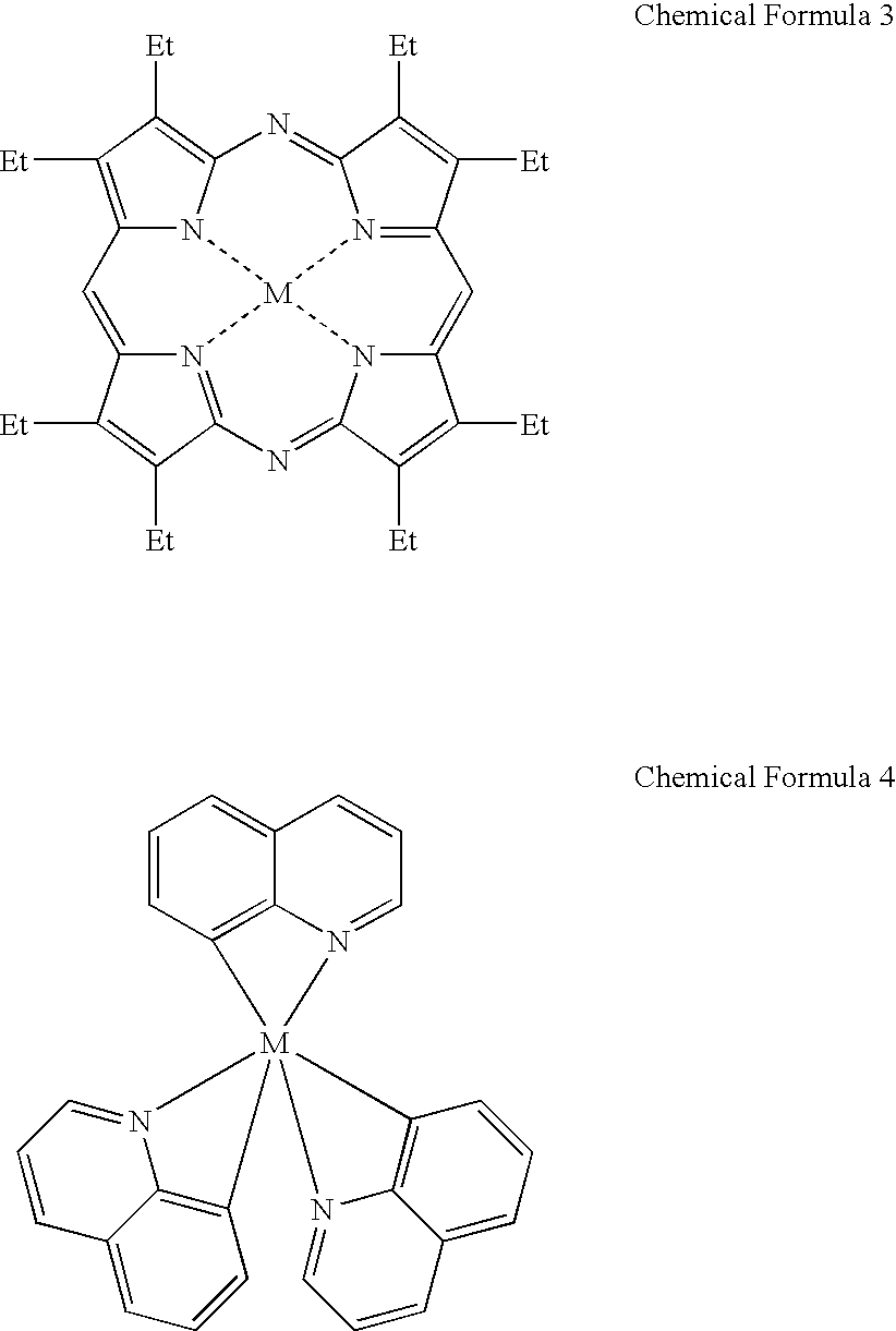
- In the above molecular formulae, M indicates an element that belongs to Groups 8 to 10 of the periodic table, Et indicated an ethyl group. In the above theses, platinum and iridium are used. Further, the inventors considers that nickel, cobalt and palladium are preferable in the reduction of manufacturing cost of a display device since they are cheaper than platinum or iridium. In particular, nickel is considered to be preferable because nickel is easy to form complex and has high productivity. In any case, the emission from the triplet excitation state (phosphorescence) has higher emission efficiency than the emission from the singlet excitation state (fluorescence), and thus, can lower operation voltage (voltage required for emission of the organic light emitting element) in obtaining the same emission luminance.
- Phthalocyanine-based CuPc, aromatic amine-based á-NPD and MTDATA, carbazole-based CBP and the like are the organic compounds in which oxygen is not included in the molecules. When oxygen or H2O is mixed into such an organic compound, the change of the bond state as described using the
chemical formulae 1 and 2 occurs, which leads to the deterioration of a hole transporting property and a light emitting property. In the formation of the layer of such an organic compound, the film forming device and the film forming method, which are described using FIGS. 1 to 3 inEmbodiment 1, are adopted. Thus, the oxygen concentration of the light emitting element can be set to 1×10¹⁹ atoms/cm3 or less. Alternatively, in the organic light emitting element having the phthalocyanine-based or aromatic amine-based hole injecting layer or hole transporting layer or the carbazole-based light emitting layer, the oxygen concentration of the hole injecting layer or hole transporting layer and in the vicinity thereof can be set to 1×10¹⁹ atoms/cm3 or less. -
FIG. 6 shows an example of a structure of an active matrix drive light emitting device. TFTs are provided in a pixel portion and various function circuits in the vicinity thereof. With respect to the TFT, either amorphous silicon or polycrystalline silicon can be selected for the material of a semiconductor film that forms a channel forming region. In the present invention, any of amorphous silicon and polycrystalline silicon may be adopted. - A glass substrate or an organic resin substrate is adopted for a
substrate 601. An organic resin material is lighter than a glass material, and thus, gives a good effect on the reduction in weight of the light emitting device itself. The organic resin materials such as polyimide, polyethylene terephthalate (PET), polyethylene naphthalate (PEN), polyether sulfone (PES) and aramide can be applied in manufacturing the light emitting device. Barium borosilicate glass or alumino borosilicate glass, which is called non-alkali glass, is desirably used for the glass substrate. The glass substrate with a thickness of 0.5 to 1.1 mm is adopted, but the thickness needs to be thinned in case of setting the purpose of attaining the reduction in weight. Further, it is desirable to adopt the glass substrate with a small specific gravity of 2.37 g/cc in order to further attain the reduction in weight. - In
FIG. 6 , an n-channel TFT 652 and a p-channel TFT 653 are formed in adriver circuit portion 650. A switchingTFT 654 and acurrent control TFT 655 are formed in apixel portion 651. These TFTs are formed on a first insulatinglayer 602 comprised of silicon nitride or silicon oxynitride (expressed by SiOxNy) by usingsemiconductor films 603 to 606, agate insulating film 607,gate electrodes 608 to 611 and the like. - A second insulating
layer 618 comprised of silicon nitride or silicon oxynitride is formed above the gate electrodes and is used as a protective film. Further, a firstinterlayer insulating film 619 comprised of an organic resin material such as polyimide or acrylic is formed as a leveling film. - The circuit structure of the
driver circuit portion 650 differs between a gate signal side driver circuit and a data signal side driver circuit, but is omitted here. The n-channel TFT 652 and the p-channel TFT 653 are connected to wirings 612 and 613, respectively, and a shift register circuit, a latch circuit, a buffer circuit and the like are formed using these TFTs. - In the
pixel portion 651, adata wiring 614 is connected to the source side of the switchingTFT 654, and awiring 615 on the drain side is connected to thegate electrode 611 of thecurrent control TFT 655. Further, the source side of thecurrent control TFT 655 is connected to a powersource supply wiring 617, and anelectrode 616 on the drain side is connected to an anode of the light emitting element. - A second
interlayer insulating film 627 comprised of an organic insulating material such as silicon nitride is formed on these wirings. The organic resin material is hygroscopic and has property in which H2O is occluded. When H2O is emitted again, oxygen is supplied to the organic compound, which becomes a cause of deterioration of the organic light emitting element. Thus, in order to prevent occlusion and re-emission of H2O, a thirdinsulating film 620 comprised of silicon nitride or silicon oxynitride is formed on the secondinterlayer insulating film 627. Alternatively, it is possible that the secondinterlayer insulating film 627 is omitted and only the thirdinsulating film 620 is formed. - Further, afuminum oxide, aluminum nitride, aluminum oxynitride and the like can be applied to the third
insulating film 620. The film formed of each of the above substances can be formed by a sputtering method using aluminum oxide or aluminum nitride as a target. - An organic
light emitting element 656 is formed on the thirdinsulating film 620 and is composed of ananode 621 formed of a transparent conductive material such as ITO (indium-tin oxide), anorganic compound layer 623 having a hole injecting layer, a hole transporting layer, a light emitting layer and the like and acathode 624 formed by using alkali metals or alkaline-earth metals such as MgAg and LiF. The detailed structure of theorganic compound layer 623 is arbitrarily adopted, but an example thereof is shown inFIGS. 5A to 5C in Embodiment 2. - The
organic compound layer 623 and thecathode 624 can not be subjected to a wet process (process such as etching with liquid medicine or washing in water). Thus, apartition layer 622 formed of a photosensitive resin material is provided on the organic insulatingfilm 619 in accordance with theanode 621. Thepartition layer 622 is formed so as to cover an end portion of theanode 621. Specifically, thepartition layer 622 is applied with a negative resist and is formed to have a thickness of approximately 1 to 2 μm after baking. Thereafter, a photo mask provided with a predetermined pattern is used, and ultraviolet rays are irradiated to thereby conduct exposure. If the negative resist material with low transmissivity is used, the ratio of the film exposed to light in the thickness direction changes. When the partition layer is developed, an end portion of the pattern can be made to have an inverse tapered shape as shown inFIG. 6 . Of course, the partition layer may be formed using photosensitive polyimide. -
FIG. 8 is a detailed diagram of a portion where the organic light emitting element is formed. After the end portion of thepartition layer 622 is formed to have the inverse tapered shape, theorganic compound layer 623 and thecathode layer 624 are formed by an evaporation method, whereby theorganic compound layer 623 and thecathode layer 624 can be formed without turning under a bottom portion of thepartition layer 622 that contacts theanode 621. Since the material for evaporation from the evaporation source adheres to the substrate with directivity in the evaporation method, the organic compound layer and the cathode layer can be formed on thecathode 621 with the state shown inFIG. 8 owing to the step of a top portion and the bottom portion of thepartition layer 622 having the inverse tapered shape. - Further,
FIG. 9 is a top view explaining the structure of the pixel portion, and the cross-sectional structure of a G-G′ line corresponds toFIG. 8 . Theanode 621 is separately formed in accordance with the TFT provided in each pixel. Thepartition layer 622 is formed so as to cover the end portion of theanode 621 and to have a stripe shape over a plurality of pixels. The organic compound layer is formed inside aregion 690 surrounded by a dotted line by evaporation. The organic compound layer is formed in accordance with thepartition layer 622 having the inverse tapered shape as shown inFIG. 8 . Thecathode 624 is similarly formed, but is formed so as to be coupled in the region external to the region where thepartition layer 622 is formed, that is, the outside of the pixel portion. - A material containing magnesium (Mg), lithium (Li) or calcium (Ca) with a small working function is used for the
cathode 624. An electrode formed of MgAg (the material in which Mg and Ag are mixed with a ratio of Mg:Ag=10:1) is preferably used. MgAgAl. LiAl, LiFAl, magnesium, magnesium alloy and magnesium compound can also be applied. Further, a fourthinsulating film 625 with a thickness of 2 to 30 nm, preferably 3 to 10 nm is formed on thecathode 624 by using silicon nitride or a DLC film. The DLC film can be formed by a plasma CVD method, and even if formed at a temperature of 100° C. or less, the DLC film can be formed covering the end portion of thepartition layer 622 with a satisfactory covering property. The internal stress of the DLC film can be relaxed by mixing a small amount of oxygen or nitrogen into the DLC film, and the DLC film can be used as a protective film. Moreover, it is known that the DLC film has a high gas-barrier property with respect to oxygen, CO, CO2 and H2O. The fourthinsulating film 625 is desirably formed in succession without exposure to an atmosphere after thecathode 624 is formed. This is because the interface state of thecathode 624 and theorganic compound layer 623 has a great influence on the emission efficiency of the organic light emitting element. - As described above, the
organic compound layer 623 and thecathode layer 624 are formed without contacting thepartition layer 622 to form the organic light emitting element, whereby the generation of a crack due to thermal stress can be prevented. Further, since an organic light emitting element most dislikes oxygen and H2O, silicon nitride or silicon oxynitride and aDLC film 625 are formed in order to block oxygen and H2O. In addition, the silicon nitride or silicon oxynitride and theDLC film 625 have also functions of not letting an alkali metal element of the organic light emitting element out. - In
FIG. 6 , the switchingTFT 654 takes a multi-gate structure, and a low density drain (LDD) that overlaps the gate electrode is provided in thecurrent control TFT 655. The TFT using polycrystalline silicon easily brings about deterioration due to hot carrier injection or the like because of the high operation speed. Therefore, the formation of the TFTs having different structures (the switching TFT with sufficiently low off current and the current control TFT that withstands the hot carrier injection) in accordance with functions in a pixel, as shown inFIG. 6 , is extremely effective in manufacturing a display device which has high reliability and enables satisfactory image display (with high operation performance). - As shown in
FIG. 6 , the first insulatingfilm 602 is formed on the lower layer side (substrate 601 side) of the semiconductor film that forms theTFTs insulating film 618 is formed. On the other hand, the thirdinsulating film 620 is formed on the lower layer side of the organiclight emitting element 656. The fourthinsulating film 625 is formed on the upper layer side. Further, the organic insulatingfilm 619 is formed between theTFTs light emitting element 656 side to integrate both the sides. Thesubstrate 601 and the organiclight emitting element 656 are considered to be the contamination source of the alkali metal such as sodium that becomes a killer impurity to theTFTs TFTs film 602 and the secondinsulating film 618, whereby the killer impurity is blocked. On the other hand, since the organiclight emitting element 656 most dislikes oxygen and H2O, the thirdinsulating film 620 and the fourth insulatingfilm 625 are formed in order to block oxygen and H2O. The thirdinsulating film 620 and the fourth insulatingfilm 625 also have functions such that the alkali metal element of the organiclight emitting element 656 do not escape. - In an organic light emitting device with the structure shown in
FIG. 6 , a step of continuously forming the thirdinsulating film 620 and theanode 621 made of a transparent conductive film typified by ITO by a sputtering method can be adopted as one example of the effective manufacturing method. The sputtering method is suitable for the formation of a fine silicon nitride film or silicon oxynitride film without remarkable damage on the surface of the organic insulatingfilm 619. - As described above, the pixel portion is formed by combining the TFT and the organic light emitting device to complete the light emitting device. In such a light emitting device, the driver circuit using the TFT may be formed on the same substrate. As shown in
FIG. 6 or 7, the semiconductor film, the gate insulating film and the gate electrode, which are the main structural components of the TFT, are surrounded by the blocking layer and the protective film which are made of silicon nitride or silicon oxynitride on the lower and upper layer sides. Thus, the TFT has the structure for preventing contamination due to the alkali metal or organic material. On the other hand, the organic light emitting element partially contains the alkali metal and is surrounded by the protective film formed of silicon nitride or silicon oxynitride and a gas-barrier layer formed of the insulating film containing silicon nitride or carbon as its main constituent. Thus, the organic light emitting element has the structure for preventing permeation of oxygen and H2O from the outside. - As described above, according to the present invention, the light emitting device can be completed by combining elements with different characteristics to the impurities without the mutual interference of the elements. Further, the influence due to the stress is eliminated to improve the reliability.
- A top gate type TFT structure is explained in
Embodiment 3. However, a bottom gate or inverted stagger type TFT may also be applied, of course. InFIG. 7 , a switchingTFT 754 and acurrent control TFT 755 are formed in apixel portion 751 by using the inverted stagger type TFTs.Gate electrodes wiring 704 formed of molybdenum or tantalum are provided on asubstrate 701, and a firstinsulating film 705 functioning as a gate insulating film is formed thereon. The firstinsulating film 705 is formed using silicon oxide or silicon nitride with a thickness of 100 to 200 nm. - In addition to a channel forming region, a source or drain region and an LDD region are formed in
semiconductor films films insulating film 710 is formed of silicon nitride or silicon oxynitride and is provided such that the semiconductor films are not contaminated by an alkali metal, organic material or the like. Further, a firstinterlayer insulating film 711 formed of an organic resin material such as polyimide is formed. Then, after contact holes are formed,wirings 713 to 716 are formed, and a secondinterlayer insulating film 719 is formed. The secondinterlayer insulating film 719 is also formed of the organic resin material such as polyimide. A thirdinsulating film 712 comprised of silicon nitride or silicon oxide is formed thereon. Thewirings 713 to 716 are formed on the thirdinsulating film 712. - An
anode 717 of an organiclight emitting element 756 is formed on the thirdinsulating film 712, and then, apartition layer 718 is formed of polyimide. The surface of thepartition layer 718 may be subjected to a plasma pre-processing by argon to make the surface finer. However, as shown inFIG. 7 , the insulatingfilm 719 comprised of a silicon nitride film is formed, and a gas emission preventing process may be conducted. The structures of anorganic compound layer 720, acathode 721 and a fourth insulating film are the same as in Embodiment 2. Thus, the light emitting device can be completed by using the inverted stagger type TFTs. - Further, a driver circuit may be formed on the same substrate by using the inverted stagger type TFTs. As shown in
FIG. 7 , the semiconductor film as the main structural component of the TFT is surrounded by the first insulating film and the second insulating film which are formed of silicon nitride or silicon oxynitride on the lower and upper layer sides. Thus, the TFT has the structure for preventing contamination of the alkali metal or organic material. On the other hand, the organic light emitting element partially contains the alkali metal and has the structure for preventing invasion of oxygen and H2O from the outside by the thirdinsulating film 712 and the fourth insulatingfilm 757. As described above, there is provided a technique of forming the light emitting device by combining elements with different characteristics to the impurities without the mutual interference of the elements even in case of using the inverted stagger type TFTs. - A structure for sealing the organic light emitting element formed in
Embodiment 3 or 4 is shown in the figure.FIG. 10 shows the state that anelement substrate 401 on which adriver circuit 408 and apixel portion 409 are formed using TFTs and a sealingsubstrate 402 are fixed by a sealingmember 405. An organiclight emitting element 403 is formed in a sealed region between theelement substrate 401 and the sealingsubstrate 402, and adrying agent 407 is provided on thedriver circuit 408 or in the vicinity of the sealingmember 405. The organiclight emitting element 403 is formed being sandwiched by the partition layers 412. - An organic resin material such as polyimide, polyethylene terephthalate (PET), polyethylene naphthalate (PEN), polyether sulfone (PES) or aramide is used for the sealing substrate. It is possible that the substrate with a thickness of about 30 to 120 μm is adopted such that the substrate has flexibility. The DLC film (fourth insulating film) 408 as a gas-barrier layer is formed at the end portion of the sealing substrate. However, the DLC film is not formed in an
external input terminal 404. An epoxy-based adhesive is used for the sealing member. TheDLC film 408 is formed along the sealingmember 405 and also along the end portions of theelement substrate 401 and the sealingsubstrate 402, whereby it is possible to prevent H2O from permeating from the above portions. -
FIG. 11 is a diagram showing an outer appearance of such a display device. The direction in which an image is displayed differs depending on the structure of the organic light emitting element. Here, the display is performed with the light emission toward the top. In the structure shown inFIG. 11 , theelement substrate 401 on which thedriver circuit portion 408 and thepixel portion 409 are formed using the TFTs and the sealingsubstrate 402 are bonded by the sealingmember 405. The partition layers 412 are formed in thepixel portion 409. Theinput terminal 404 is provided at the end portion of theelement substrate 401 and is connected to a flexible printed circuit (FPC). The terminals for inputting an image data signal, various timing signals and a power source from an external circuit are provided at 500 μm intervals in theinput terminal 404. Theinput terminal 404 is connected to the driver circuit portion through awiring 410. Further, anIC chip 411 in which a CPU, a memory and the like are formed may be mounted to theelement substrate 401 by a COG (chip on glass) method if necessary. - The DLC film is formed at the end portions of the substrates and prevents deterioration of the organic light emitting element due to permeation of water vapor, oxygen and the like from the sealed portion. In the case where the organic resin material is used for the
element substrate 401 or the sealingsubstrate 402, the DLC film may be formed over the entire surface except the input terminal portion. When the DLC film is formed, the input terminal portion may be covered in advance by using a masking tape or a shadow mask. - As described above, the light emitting device can be formed by sealing the organic light emitting element formed in
Embodiment 3 or 4. The structure of the light emitting device is such that the TFT and the organic light emitting element are both surrounded by the insulating films and the impurities do not permeate from the outside. Further, the element substrate and the sealing substrate are bonded to each other by using the sealing member, and the end portions are covered with the DLC film to thereby improve airtightness. Thus, the deterioration of the light emitting device can be prevented. - The present invention can be applied to a display medium used in various electronic devices. As such electronic devices, a portable information terminal (electronic notebook, mobile computer, portable telephone or the like), a video camera, a digital camera, a personal computer, a television set, a portable telephone, and the like can be given. Examples thereof are shown in
FIGS. 13A to 13G. -
FIG. 13A shows a television set completed by applying the light emitting device of the present invention, which is constituted of acasing 3001, asupport base 3002, adisplay portion 3003 and the like. The light emitting device of the present invention is applied to thedisplay portion 3003. -
FIG. 13B shows a video camera completed by applying the light emitting device of the present invention, which is constituted of amain body 3011, adisplay portion 3012, asound input portion 3013, operation switches 3014, abattery 3015, animage receiving portion 3016 and the like. The light emitting device of the present invention is applied to thedisplay portion 3012. -
FIG. 13C shows a note-type personal computer completed by applying the light emitting device of the present invention, which is constituted of amain body 3021, acasing 3022, adisplay portion 3023, akeyboard 3024 and the like. The light emitting device of the present invention is applied to thedisplay portion 3023. -
FIG. 13D shows a PDA (personal digital assistant) completed by applying the light emitting device of the present invention, which is constituted of amain body 3031, astylus 3032, adisplay portion 3033,operation buttons 3034, anexternal interface 3035 and the like. The light emitting device of the present invention can be applied to thedisplay portion 3033. -
FIG. 13E shows a sound playback device completed by applying the light emitting device of the present invention, specifically, an audio device for automobile, which is constituted of amain body 3041, adisplay portion 3042, operation switches 3043, 3044 and the like. The light emitting device of the present invention can be applied to thedisplay portion 3042. -
FIG. 13F shows a digital camera completed by applying the light emitting device of the present invention, which is constituted of amain body 3051, a display portion (A) 3052, aneyepiece portion 3053, operation switches 3054, a display portion (B) 3055, abattery 3056 and the like. The light emitting device of the present invention can be applied to the display portion (A) 3052 and the display portion (B) 3055. -
FIG. 13G shows a portable telephone completed by applying the light emitting device of the present invention, which is constituted of amain body 3061, asound output portion 3062, asound input portion 3063, adisplay portion 3064, operation switches 3065, anantenna 3066 and the like. The light emitting device of the present invention can be applied to thedisplay portion 3064. - Note that the electronic devices shown here are some examples, and the present invention is not limited to these applications.
- As described above, the deterioration due to the stress of the organic light emitting element can be prevented by applying the present invention. Further, in the present invention, the semiconductor film, the gate insulating film and the gate electrode, which are the main structural components of the TFT, are surrounded by the first insulating layer and the second insulating layer which are formed of silicon nitride or silicon oxynitride on the lower layer side and the upper layer side. Thus, the TFT has the structure for preventing contamination due to the alkali metal or organic material. On the other hand, the organic light emitting element partially contains the alkali metal and is surrounded by the third insulating layer formed of silicon nitride or silicon oxynitride and the fourth insulating layer formed of the insulating film containing carbon as its main constituent. Thus, the structure for preventing permeation of oxygen and H2O from the outside is realized in the organic light emitting element. Accordingly, the light emitting device can be completed by combining the elements with different characteristics to the impurities without the mutual interference of the elements.
Claims (31)
Priority Applications (1)
| Application Number | Priority Date | Filing Date | Title |
|---|---|---|---|
| US11/003,381 US7633223B2 (en) | 2000-11-10 | 2004-12-06 | Organic light emitting device provided with drying agent at side surfaces of a sealing member |
Applications Claiming Priority (4)
| Application Number | Priority Date | Filing Date | Title |
|---|---|---|---|
| JP2000342739 | 2000-11-10 | ||
| JP2000-342739 | 2000-11-10 | ||
| US09/986,425 US6828727B2 (en) | 2000-11-10 | 2001-11-08 | Light emitting device comprising a partition layer having an overhang shape |
| US11/003,381 US7633223B2 (en) | 2000-11-10 | 2004-12-06 | Organic light emitting device provided with drying agent at side surfaces of a sealing member |
Related Parent Applications (1)
| Application Number | Title | Priority Date | Filing Date |
|---|---|---|---|
| US09/986,425 Continuation US6828727B2 (en) | 2000-11-10 | 2001-11-08 | Light emitting device comprising a partition layer having an overhang shape |
Publications (2)
| Publication Number | Publication Date |
|---|---|
| US20050093436A1 true US20050093436A1 (en) | 2005-05-05 |
| US7633223B2 US7633223B2 (en) | 2009-12-15 |
Family
ID=18817231
Family Applications (2)
| Application Number | Title | Priority Date | Filing Date |
|---|---|---|---|
| US09/986,425 Expired - Lifetime US6828727B2 (en) | 2000-11-10 | 2001-11-08 | Light emitting device comprising a partition layer having an overhang shape |
| US11/003,381 Expired - Fee Related US7633223B2 (en) | 2000-11-10 | 2004-12-06 | Organic light emitting device provided with drying agent at side surfaces of a sealing member |
Family Applications Before (1)
| Application Number | Title | Priority Date | Filing Date |
|---|---|---|---|
| US09/986,425 Expired - Lifetime US6828727B2 (en) | 2000-11-10 | 2001-11-08 | Light emitting device comprising a partition layer having an overhang shape |
Country Status (4)
| Country | Link |
|---|---|
| US (2) | US6828727B2 (en) |
| KR (2) | KR100838504B1 (en) |
| CN (2) | CN1905206B (en) |
| TW (1) | TW522577B (en) |
Cited By (13)
| Publication number | Priority date | Publication date | Assignee | Title |
|---|---|---|---|---|
| US20030089913A1 (en) * | 2001-06-18 | 2003-05-15 | Semiconductor Energy Laboratory Co., Ltd. | Light emitting device and method of fabricating the same |
| US20040079950A1 (en) * | 2002-09-20 | 2004-04-29 | Toru Takayama | Light-emitting apparatus and fabrication method of the same |
| US20050005848A1 (en) * | 2003-04-25 | 2005-01-13 | Shunpei Yamazaki | Apparatus for forming a film and an electroluminescence device |
| US20050212420A1 (en) * | 2004-03-26 | 2005-09-29 | Semiconductor Energy Laboratory Co., Ltd. | Light emitting device and manufacturing method thereof |
| US20060186399A1 (en) * | 2002-10-18 | 2006-08-24 | Semiconductor Energy Laboratory Co., Ltd., A Japan Corporation | Semiconductor apparatus and fabrication method of the same |
| US20060186413A1 (en) * | 2004-10-01 | 2006-08-24 | Semiconductor Energy Laboratory Co., Ltd. | Display device and manufacturing method of the same |
| US20070164667A1 (en) * | 2006-01-16 | 2007-07-19 | Samsung Electronics Co., Ltd | Display device and manufacturing method of the same |
| US20070187761A1 (en) * | 2001-01-19 | 2007-08-16 | Semiconductor Energy Laboratory Co., Ltd. | Semiconductor device and method of manufacturing the same |
| US20070228382A1 (en) * | 2002-06-11 | 2007-10-04 | Shunpei Yamazaki | Light emitting device and manufacturing method thereof |
| US20090001886A1 (en) * | 2007-06-28 | 2009-01-01 | Semiconductor Energy Laboratory Co., Ltd. | Light-emitting element, light-emitting device, electronic device, and method for fabricating light-emitting element |
| US9105855B2 (en) | 2004-05-20 | 2015-08-11 | Semiconductor Energy Laboratory Co., Ltd. | Light-emitting element and display device |
| US9166180B2 (en) | 2001-06-20 | 2015-10-20 | Semiconductor Energy Laboratory Co., Ltd. | Light emitting device having an organic light emitting diode that emits white light |
| CN107799564A (en) * | 2016-08-31 | 2018-03-13 | 乐金显示有限公司 | Organic light emitting array and use its organic light-emitting display device |
Families Citing this family (63)
| Publication number | Priority date | Publication date | Assignee | Title |
|---|---|---|---|---|
| US6664732B2 (en) * | 2000-10-26 | 2003-12-16 | Semiconductor Energy Laboratory Co., Ltd. | Light emitting device and manufacturing method thereof |
| SG143942A1 (en) * | 2001-02-19 | 2008-07-29 | Semiconductor Energy Lab | Light emitting device and method of manufacturing the same |
| US7211828B2 (en) | 2001-06-20 | 2007-05-01 | Semiconductor Energy Laboratory Co., Ltd. | Light emitting device and electronic apparatus |
| US6852997B2 (en) | 2001-10-30 | 2005-02-08 | Semiconductor Energy Laboratory Co., Ltd. | Light emitting device |
| US6903377B2 (en) * | 2001-11-09 | 2005-06-07 | Semiconductor Energy Laboratory Co., Ltd. | Light emitting apparatus and method for manufacturing the same |
| US7042024B2 (en) * | 2001-11-09 | 2006-05-09 | Semiconductor Energy Laboratory Co., Ltd. | Light emitting apparatus and method for manufacturing the same |
| US6822264B2 (en) * | 2001-11-16 | 2004-11-23 | Semiconductor Energy Laboratory Co., Ltd. | Light emitting device |
| JP4101511B2 (en) * | 2001-12-27 | 2008-06-18 | 株式会社半導体エネルギー研究所 | Light emitting device and manufacturing method thereof |
| US7098069B2 (en) | 2002-01-24 | 2006-08-29 | Semiconductor Energy Laboratory Co., Ltd. | Light emitting device, method of preparing the same and device for fabricating the same |
| TWI275319B (en) * | 2002-02-05 | 2007-03-01 | Semiconductor Energy Lab | Manufacturing method and method of operating a manufacturing apparatus |
| TWI286044B (en) * | 2002-02-22 | 2007-08-21 | Semiconductor Energy Lab | Light-emitting device and method of manufacturing the same, and method of operating manufacturing apparatus |
| JP4017441B2 (en) * | 2002-04-26 | 2007-12-05 | 三洋電機株式会社 | Organic EL panel and manufacturing method thereof |
| KR100474906B1 (en) * | 2002-06-07 | 2005-03-10 | 엘지전자 주식회사 | Active Matrix Organic Electro-Luminescence Device |
| KR100864001B1 (en) | 2002-06-14 | 2008-10-16 | 삼성전자주식회사 | Organic electroluminescent device |
| CN100385705C (en) * | 2002-07-12 | 2008-04-30 | 铼宝科技股份有限公司 | Initiative driving type organic electric excitation lighting equipment |
| JP2004095482A (en) * | 2002-09-03 | 2004-03-25 | Chi Mei Electronics Corp | Image display device |
| WO2004026002A1 (en) | 2002-09-11 | 2004-03-25 | Semiconductor Energy Laboratory Co., Ltd. | Light-emitting apparatus and fabrication method of the same |
| WO2004025999A1 (en) * | 2002-09-12 | 2004-03-25 | Ifire Technology Corp. | Silicon oxynitride passivated rare earth activated thioaluminate phosphors for electroluminescent displays |
| US20040124421A1 (en) * | 2002-09-20 | 2004-07-01 | Semiconductor Energy Laboratory Co., Ltd. | Light-emitting device and manufacturing method thereof |
| JP2004119016A (en) * | 2002-09-20 | 2004-04-15 | Semiconductor Energy Lab Co Ltd | Light emitting device |
| US20040099926A1 (en) * | 2002-11-22 | 2004-05-27 | Semiconductor Energy Laboratory Co., Ltd. | Semiconductor device, display device, and light-emitting device, and methods of manufacturing the same |
| CN1820551B (en) | 2002-12-20 | 2010-10-06 | 伊菲雷知识产权公司 | Aluminum nitride passivated phosphors for electroluminescent displays |
| JP4170138B2 (en) * | 2003-04-28 | 2008-10-22 | 三菱電機株式会社 | Organic electroluminescent device and manufacturing method thereof |
| SG142140A1 (en) | 2003-06-27 | 2008-05-28 | Semiconductor Energy Lab | Display device and method of manufacturing thereof |
| US20050057154A1 (en) * | 2003-07-30 | 2005-03-17 | Optrex Corporation | Organic EL display device and method for fabricating the same |
| JP4823478B2 (en) * | 2003-09-19 | 2011-11-24 | 株式会社半導体エネルギー研究所 | Method for manufacturing light emitting device |
| US7619258B2 (en) * | 2004-03-16 | 2009-11-17 | Semiconductor Energy Laboratory Co., Ltd. | Display device |
| CN100358172C (en) * | 2004-04-14 | 2007-12-26 | 友达光电股份有限公司 | Active organic electrolumniescence device and its mfg. method |
| JP2005317229A (en) * | 2004-04-27 | 2005-11-10 | Seiko Epson Corp | Manufacturing method of organic el device, and electronic apparatus |
| KR100700012B1 (en) * | 2004-11-25 | 2007-03-26 | 삼성에스디아이 주식회사 | Organic electro luminescence display and methode for manufacturing the same |
| US8101990B2 (en) * | 2005-05-31 | 2012-01-24 | Semiconductor Energy Laboratory Co., Ltd. | Semiconductor device |
| KR20070054806A (en) * | 2005-11-24 | 2007-05-30 | 삼성전자주식회사 | Organic light emitting diode display |
| US20080006819A1 (en) * | 2006-06-19 | 2008-01-10 | 3M Innovative Properties Company | Moisture barrier coatings for organic light emitting diode devices |
| JP4531850B2 (en) * | 2007-03-23 | 2010-08-25 | パイオニア株式会社 | Organic transistor and manufacturing method thereof |
| KR101296656B1 (en) * | 2008-06-24 | 2013-08-14 | 엘지디스플레이 주식회사 | Organic Light Emitting Display Device and Method For Fabricating the Same |
| KR101147428B1 (en) * | 2009-02-09 | 2012-05-23 | 삼성모바일디스플레이주식회사 | Organic light emitting diode display |
| KR101653844B1 (en) * | 2010-04-19 | 2016-09-02 | 가부시키가이샤 제이올레드 | Organic el display panel and oraganic el display apparatus having the same and method of manufacturing organic el display panel |
| WO2012115016A1 (en) | 2011-02-25 | 2012-08-30 | Semiconductor Energy Laboratory Co., Ltd. | Light-emitting device and electronic device using light-emitting device |
| US9142598B2 (en) | 2011-06-24 | 2015-09-22 | Semiconductor Energy Laboratory Co., Ltd. | Light-emitting panel, light-emitting device using the light-emitting panel, and method for manufacturing the light-emitting panel |
| KR101933952B1 (en) | 2011-07-01 | 2018-12-31 | 가부시키가이샤 한도오따이 에네루기 켄큐쇼 | Light-emitting device, electronic device, and lighting device |
| KR102082793B1 (en) | 2012-05-10 | 2020-02-28 | 가부시키가이샤 한도오따이 에네루기 켄큐쇼 | Display device and method for manufacturing the same |
| US8658444B2 (en) | 2012-05-16 | 2014-02-25 | International Business Machines Corporation | Semiconductor active matrix on buried insulator |
| EP2879466B1 (en) * | 2012-07-27 | 2019-10-09 | Mitsui Mining and Smelting Co., Ltd. | Metal foil and electronic device |
| JP6302186B2 (en) * | 2012-08-01 | 2018-03-28 | 株式会社半導体エネルギー研究所 | Display device |
| KR101967600B1 (en) * | 2012-11-09 | 2019-04-10 | 엘지디스플레이 주식회사 | Flexible organic electroluminescent device and method for fabricating the same |
| KR102493535B1 (en) | 2013-07-12 | 2023-02-01 | 가부시키가이샤 한도오따이 에네루기 켄큐쇼 | Light-emitting device |
| KR102288238B1 (en) | 2013-09-03 | 2021-08-09 | 가부시키가이샤 한도오따이 에네루기 켄큐쇼 | Light-emitting device |
| KR102358935B1 (en) | 2014-02-12 | 2022-02-04 | 가부시키가이샤 한도오따이 에네루기 켄큐쇼 | Electronic device |
| TWI654736B (en) | 2014-02-14 | 2019-03-21 | 日商半導體能源研究所股份有限公司 | Illuminating device |
| WO2015128778A1 (en) | 2014-02-28 | 2015-09-03 | Semiconductor Energy Laboratory Co., Ltd. | Electronic device |
| US10372163B2 (en) | 2014-05-30 | 2019-08-06 | Semiconductor Energy Laboratory Co., Ltd. | Input device comprising sensor panel, information processing device comprising input device |
| JP6594013B2 (en) * | 2014-06-17 | 2019-10-23 | キヤノン株式会社 | Organic light emitting device and method for manufacturing the same |
| KR20160047673A (en) * | 2014-10-22 | 2016-05-03 | 삼성디스플레이 주식회사 | Organic light emitting display apparatus and the fabrication method thereof |
| KR20210068638A (en) | 2014-10-28 | 2021-06-09 | 가부시키가이샤 한도오따이 에네루기 켄큐쇼 | Light-emitting device |
| KR102357269B1 (en) * | 2014-12-12 | 2022-02-03 | 삼성디스플레이 주식회사 | Organic light emitting display device and method of manufacturing the same |
| KR102365778B1 (en) * | 2015-02-24 | 2022-02-21 | 삼성디스플레이 주식회사 | Organic light emitting display device and method for manufacturing the same |
| CN105826355B (en) * | 2016-05-03 | 2017-03-08 | 京东方科技集团股份有限公司 | A kind of preparation method of display floater |
| CN106531768A (en) * | 2016-12-07 | 2017-03-22 | 厦门天马微电子有限公司 | Organic electroluminescence display panel and preparation method thereof |
| CN106920828B (en) * | 2017-03-29 | 2019-11-05 | 京东方科技集团股份有限公司 | A kind of organic electroluminescent display panel and preparation method |
| CN109920816B (en) * | 2017-12-12 | 2021-03-30 | 京东方科技集团股份有限公司 | Display substrate, manufacturing method thereof and display device |
| CN108110037B (en) * | 2017-12-29 | 2020-09-04 | 昆山国显光电有限公司 | Flexible display screen |
| CN108962964B (en) * | 2018-08-01 | 2020-06-30 | 京东方科技集团股份有限公司 | Display panel, preparation method thereof and display device |
| WO2020208774A1 (en) * | 2019-04-11 | 2020-10-15 | シャープ株式会社 | Light-emitting element and display device |
Citations (25)
| Publication number | Priority date | Publication date | Assignee | Title |
|---|---|---|---|---|
| US5684365A (en) * | 1994-12-14 | 1997-11-04 | Eastman Kodak Company | TFT-el display panel using organic electroluminescent media |
| US5701055A (en) * | 1994-03-13 | 1997-12-23 | Pioneer Electronic Corporation | Organic electoluminescent display panel and method for manufacturing the same |
| US5952037A (en) * | 1995-03-13 | 1999-09-14 | Pioneer Electronic Corporation | Organic electroluminescent display panel and method for manufacturing the same |
| US5952708A (en) * | 1995-11-17 | 1999-09-14 | Semiconductor Energy Laboratory Co., Ltd. | Display device |
| US6016033A (en) * | 1997-07-11 | 2000-01-18 | Fed Corporation | Electrode structure for high resolution organic light-emitting diode displays and method for making the same |
| US6037712A (en) * | 1996-06-10 | 2000-03-14 | Tdk Corporation | Organic electroluminescence display device and producing method thereof |
| US6057647A (en) * | 1998-02-24 | 2000-05-02 | Casio Computer Co., Ltd. | Light emitting device used for display device |
| US6069443A (en) * | 1997-06-23 | 2000-05-30 | Fed Corporation | Passive matrix OLED display |
| US6114183A (en) * | 1996-12-11 | 2000-09-05 | Sanyo Electric Co., Ltd. | Display apparatus using electroluminescence elements and method of manufacturing same |
| US6115090A (en) * | 1997-03-26 | 2000-09-05 | Semiconductor Energy Laboratory Co., Ltd. | Display device |
| US6157127A (en) * | 1996-03-12 | 2000-12-05 | Idemitsu Kosan Co., Ltd. | Organic electroluminescent element and organic electroluminescent display |
| US6225750B1 (en) * | 1999-01-29 | 2001-05-01 | Seiko Epson Corporation | Display device |
| US20010002144A1 (en) * | 1997-03-26 | 2001-05-31 | Shunpei Yamazaki | Display device |
| US6281634B1 (en) * | 1998-12-01 | 2001-08-28 | Sanyo Electric Co., Ltd. | Color electroluminescence display device |
| US20020000551A1 (en) * | 2000-03-06 | 2002-01-03 | Shunpei Yamazaki | Semiconductor device and manufacturing method thereof |
| US20020024096A1 (en) * | 2000-08-18 | 2002-02-28 | Shunpei Yamazaki | Light-emitting device and display device |
| US6359606B1 (en) * | 1997-08-29 | 2002-03-19 | Seiko Epson Corporation | Active matrix display |
| US20020057055A1 (en) * | 2000-10-26 | 2002-05-16 | Shunpei Yamazaki | Light emitting device and manufacturing method thereof |
| US6429599B1 (en) * | 1998-12-01 | 2002-08-06 | Sanyo Electric Co., Ltd. | Color electroluminescence display device |
| US6433486B1 (en) * | 1998-12-01 | 2002-08-13 | Sanyo Electric Co., Ltd. | Color electroluminescence display device |
| US6498049B1 (en) * | 1998-02-23 | 2002-12-24 | Cambridge Display Technology | Display devices |
| US6621213B2 (en) * | 2000-08-22 | 2003-09-16 | Sony Corporation | Organic electroluminescence device and manufacturing method therefor |
| US6630784B2 (en) * | 1998-02-27 | 2003-10-07 | Sanyo Electric Co., Ltd. | Electroluminescence display apparatus having an opaque anode electrode and manufacturing method thereof |
| US20050197031A1 (en) * | 1999-06-04 | 2005-09-08 | Semiconductor Energy Laboratory Co., Ltd. | Method for manufacturing an electro-optical device |
| US7015503B2 (en) * | 1998-03-17 | 2006-03-21 | Seiko Epson Corporation | Method of forming thin film patterning substrate including formation of banks |
Family Cites Families (23)
| Publication number | Priority date | Publication date | Assignee | Title |
|---|---|---|---|---|
| JPS5835639B2 (en) | 1980-04-21 | 1983-08-03 | 株式会社 キヨウシン | Solid fuel manufacturing method |
| JP3197305B2 (en) | 1991-10-08 | 2001-08-13 | ティーディーケイ株式会社 | Protection of electroluminescent element |
| JPH06124785A (en) | 1992-10-08 | 1994-05-06 | Idemitsu Kosan Co Ltd | Organic el element |
| JPH0736024A (en) | 1993-07-20 | 1995-02-07 | Sharp Corp | Production of substrate |
| JP3813217B2 (en) | 1995-03-13 | 2006-08-23 | パイオニア株式会社 | Method for manufacturing organic electroluminescence display panel |
| US6175186B1 (en) * | 1996-02-26 | 2001-01-16 | Idemitsu Kosan Co., Ltd. | Organic electroluminescent element and method for manufacturing the same |
| JP4011649B2 (en) | 1996-06-11 | 2007-11-21 | 出光興産株式会社 | Multicolor light emitting device and manufacturing method thereof |
| JPH1039334A (en) * | 1996-07-24 | 1998-02-13 | Toshiba Corp | Array substrate and liquid crystal display device |
| JP3524711B2 (en) | 1997-03-18 | 2004-05-10 | 三洋電機株式会社 | Organic electroluminescence device and method of manufacturing the same |
| JP3570857B2 (en) | 1997-05-20 | 2004-09-29 | パイオニア株式会社 | Organic EL display panel and manufacturing method thereof |
| JP3886219B2 (en) * | 1997-07-29 | 2007-02-28 | 株式会社アルバック | Organic EL device |
| JP3663876B2 (en) * | 1998-01-08 | 2005-06-22 | 松下電器産業株式会社 | Organic electroluminescent device and method for manufacturing the same |
| TW420964B (en) * | 1998-02-25 | 2001-02-01 | Toppan Printing Co Ltd | Organic electroluminescence display substrate, method of manufacturing it and organic electroluminescent display element |
| JP3910303B2 (en) * | 1998-02-25 | 2007-04-25 | 凸版印刷株式会社 | Method for manufacturing substrate for organic electroluminescence display element |
| WO2000072637A1 (en) | 1998-03-09 | 2000-11-30 | Tdk Corporation | Organic el color display |
| JPH11260562A (en) | 1998-03-09 | 1999-09-24 | Tdk Corp | Organic el color display |
| JPH11317288A (en) * | 1998-04-30 | 1999-11-16 | Toyota Motor Corp | Manufacture of organic el display panel |
| JP2000133460A (en) | 1998-10-21 | 2000-05-12 | Toyota Motor Corp | El display panel and its manufacture |
| TW439387B (en) * | 1998-12-01 | 2001-06-07 | Sanyo Electric Co | Display device |
| JP2000243557A (en) | 1998-12-22 | 2000-09-08 | Toray Ind Inc | Organic electroluminescence element and its manufacture |
| JP4186289B2 (en) | 1998-12-24 | 2008-11-26 | 凸版印刷株式会社 | Method for producing substrate for organic electroluminescence display element and method for producing organic electroluminescence display element |
| JP3814102B2 (en) | 1999-05-24 | 2006-08-23 | 東北パイオニア株式会社 | Organic EL display panel and manufacturing method thereof |
| KR20010109639A (en) * | 2000-05-31 | 2001-12-12 | 주식회사 현대 디스플레이 테크놀로지 | Method for manufacturing organic el display |
-
2001
- 2001-10-25 TW TW090126437A patent/TW522577B/en not_active IP Right Cessation
- 2001-11-08 US US09/986,425 patent/US6828727B2/en not_active Expired - Lifetime
- 2001-11-10 KR KR1020010069922A patent/KR100838504B1/en not_active IP Right Cessation
- 2001-11-12 CN CN2006101090369A patent/CN1905206B/en not_active Expired - Fee Related
- 2001-11-12 CN CNB011374527A patent/CN1276520C/en not_active Expired - Fee Related
-
2004
- 2004-12-06 US US11/003,381 patent/US7633223B2/en not_active Expired - Fee Related
-
2006
- 2006-11-10 KR KR1020060111121A patent/KR100868667B1/en active IP Right Grant
Patent Citations (45)
| Publication number | Priority date | Publication date | Assignee | Title |
|---|---|---|---|---|
| US5701055A (en) * | 1994-03-13 | 1997-12-23 | Pioneer Electronic Corporation | Organic electoluminescent display panel and method for manufacturing the same |
| US5684365A (en) * | 1994-12-14 | 1997-11-04 | Eastman Kodak Company | TFT-el display panel using organic electroluminescent media |
| US5952037A (en) * | 1995-03-13 | 1999-09-14 | Pioneer Electronic Corporation | Organic electroluminescent display panel and method for manufacturing the same |
| US5952708A (en) * | 1995-11-17 | 1999-09-14 | Semiconductor Energy Laboratory Co., Ltd. | Display device |
| US6239470B1 (en) * | 1995-11-17 | 2001-05-29 | Semiconductor Energy Laboratory Co., Ltd. | Active matrix electro-luminescent display thin film transistor |
| US6169293B1 (en) * | 1995-11-17 | 2001-01-02 | Semiconductor Energy Labs | Display device |
| US6157127A (en) * | 1996-03-12 | 2000-12-05 | Idemitsu Kosan Co., Ltd. | Organic electroluminescent element and organic electroluminescent display |
| US6037712A (en) * | 1996-06-10 | 2000-03-14 | Tdk Corporation | Organic electroluminescence display device and producing method thereof |
| US6114183A (en) * | 1996-12-11 | 2000-09-05 | Sanyo Electric Co., Ltd. | Display apparatus using electroluminescence elements and method of manufacturing same |
| US6115090A (en) * | 1997-03-26 | 2000-09-05 | Semiconductor Energy Laboratory Co., Ltd. | Display device |
| US20010002144A1 (en) * | 1997-03-26 | 2001-05-31 | Shunpei Yamazaki | Display device |
| US6069443A (en) * | 1997-06-23 | 2000-05-30 | Fed Corporation | Passive matrix OLED display |
| US6016033A (en) * | 1997-07-11 | 2000-01-18 | Fed Corporation | Electrode structure for high resolution organic light-emitting diode displays and method for making the same |
| US6359606B1 (en) * | 1997-08-29 | 2002-03-19 | Seiko Epson Corporation | Active matrix display |
| US6734839B2 (en) * | 1997-08-29 | 2004-05-11 | Seiko Epson Corporation | Active matrix display device |
| US6498049B1 (en) * | 1998-02-23 | 2002-12-24 | Cambridge Display Technology | Display devices |
| US6057647A (en) * | 1998-02-24 | 2000-05-02 | Casio Computer Co., Ltd. | Light emitting device used for display device |
| US6951495B2 (en) * | 1998-02-27 | 2005-10-04 | Sanyo Electric Co., Ltd. | Display apparatus having electroluminescence elements |
| US6630784B2 (en) * | 1998-02-27 | 2003-10-07 | Sanyo Electric Co., Ltd. | Electroluminescence display apparatus having an opaque anode electrode and manufacturing method thereof |
| US7214959B2 (en) * | 1998-03-17 | 2007-05-08 | Seiko Epson Corporation | Method of forming thin film patterning substrate including formation of banks |
| US7273801B2 (en) * | 1998-03-17 | 2007-09-25 | Seiko Epson Corporation | Method of forming thin film patterning substrate including formation of banks |
| US7015503B2 (en) * | 1998-03-17 | 2006-03-21 | Seiko Epson Corporation | Method of forming thin film patterning substrate including formation of banks |
| US7442955B2 (en) * | 1998-03-17 | 2008-10-28 | Seiko Epson Corporation | Method of forming thin film patterning substrate including formation of banks |
| US20090020751A1 (en) * | 1998-03-17 | 2009-01-22 | Seiko Epson Corporation | Method of forming thin film patterning substrate including formation of banks |
| US6433486B1 (en) * | 1998-12-01 | 2002-08-13 | Sanyo Electric Co., Ltd. | Color electroluminescence display device |
| US6995517B2 (en) * | 1998-12-01 | 2006-02-07 | Sanyo Electric Co., Ltd. | Color electroluminescence display device |
| US6281634B1 (en) * | 1998-12-01 | 2001-08-28 | Sanyo Electric Co., Ltd. | Color electroluminescence display device |
| US7339559B2 (en) * | 1998-12-01 | 2008-03-04 | Sanyo Electric Co., Ltd. | Color electroluminescence display device |
| US7315131B2 (en) * | 1998-12-01 | 2008-01-01 | Sanyo Electric Co., Ltd. | Color electroluminescence display device |
| US6429599B1 (en) * | 1998-12-01 | 2002-08-06 | Sanyo Electric Co., Ltd. | Color electroluminescence display device |
| US6690118B2 (en) * | 1998-12-01 | 2004-02-10 | Sanyo Electric Co., Ltd. | Color electroluminescence display device |
| US6642665B2 (en) * | 1999-01-29 | 2003-11-04 | Seiko Epson Corporation | Display device |
| US6225750B1 (en) * | 1999-01-29 | 2001-05-01 | Seiko Epson Corporation | Display device |
| US6388389B2 (en) * | 1999-01-29 | 2002-05-14 | Seiko Epson Corporation | Display device |
| US6469450B2 (en) * | 1999-01-29 | 2002-10-22 | Seiko Epson Corporation | Display device |
| US20050197031A1 (en) * | 1999-06-04 | 2005-09-08 | Semiconductor Energy Laboratory Co., Ltd. | Method for manufacturing an electro-optical device |
| US20050206313A1 (en) * | 1999-06-04 | 2005-09-22 | Semiconductor Energy Laboratory Co., Ltd. | Method for manufacturing an electro-optical device |
| US7393707B2 (en) * | 1999-06-04 | 2008-07-01 | Semiconductor Energy Laboratory Co., Ltd. | Method for manufacturing an electro-optical device |
| US7288420B1 (en) * | 1999-06-04 | 2007-10-30 | Semiconductor Energy Laboratory Co., Ltd. | Method for manufacturing an electro-optical device |
| US20020000551A1 (en) * | 2000-03-06 | 2002-01-03 | Shunpei Yamazaki | Semiconductor device and manufacturing method thereof |
| US20020024096A1 (en) * | 2000-08-18 | 2002-02-28 | Shunpei Yamazaki | Light-emitting device and display device |
| US6605826B2 (en) * | 2000-08-18 | 2003-08-12 | Semiconductor Energy Laboratory Co., Ltd. | Light-emitting device and display device |
| US6621213B2 (en) * | 2000-08-22 | 2003-09-16 | Sony Corporation | Organic electroluminescence device and manufacturing method therefor |
| US6664732B2 (en) * | 2000-10-26 | 2003-12-16 | Semiconductor Energy Laboratory Co., Ltd. | Light emitting device and manufacturing method thereof |
| US20020057055A1 (en) * | 2000-10-26 | 2002-05-16 | Shunpei Yamazaki | Light emitting device and manufacturing method thereof |
Cited By (39)
| Publication number | Priority date | Publication date | Assignee | Title |
|---|---|---|---|---|
| US20070187761A1 (en) * | 2001-01-19 | 2007-08-16 | Semiconductor Energy Laboratory Co., Ltd. | Semiconductor device and method of manufacturing the same |
| US20030089913A1 (en) * | 2001-06-18 | 2003-05-15 | Semiconductor Energy Laboratory Co., Ltd. | Light emitting device and method of fabricating the same |
| US9276224B2 (en) | 2001-06-20 | 2016-03-01 | Semiconductor Energy Laboratory Co., Ltd. | Organic light emitting device having dual flexible substrates |
| US9178168B2 (en) | 2001-06-20 | 2015-11-03 | Semiconductor Energy Laboratory Co., Ltd. | White light emitting device |
| US9166180B2 (en) | 2001-06-20 | 2015-10-20 | Semiconductor Energy Laboratory Co., Ltd. | Light emitting device having an organic light emitting diode that emits white light |
| US8362487B2 (en) | 2002-06-11 | 2013-01-29 | Semiconductor Energy Laboratory Co., Ltd. | Light emitting device comprising film having hygroscopic property and transparency |
| US20070228382A1 (en) * | 2002-06-11 | 2007-10-04 | Shunpei Yamazaki | Light emitting device and manufacturing method thereof |
| US7453094B2 (en) | 2002-09-20 | 2008-11-18 | Semiconductor Energy Laboratory Co., Ltd. | Light-emitting apparatus and fabrication method of the same |
| US20040079950A1 (en) * | 2002-09-20 | 2004-04-29 | Toru Takayama | Light-emitting apparatus and fabrication method of the same |
| US20090152539A1 (en) * | 2002-10-18 | 2009-06-18 | Semiconductor Energy Laboratory Co., Ltd. | Semiconductor Apparatus and Fabrication Method of the Same |
| US9093324B2 (en) | 2002-10-18 | 2015-07-28 | Semiconductor Energy Laboratory Co., Ltd. | Semiconductor apparatus and fabrication method of the same |
| US7495256B2 (en) | 2002-10-18 | 2009-02-24 | Semiconductor Energy Laboratory Co., Ltd. | Semiconductor apparatus and fabrication method of the same |
| US20060186399A1 (en) * | 2002-10-18 | 2006-08-24 | Semiconductor Energy Laboratory Co., Ltd., A Japan Corporation | Semiconductor apparatus and fabrication method of the same |
| US8525171B2 (en) | 2002-10-18 | 2013-09-03 | Semiconductor Energy Laboratory Co., Ltd. | Semiconductor apparatus and fabrication method of the same |
| US20110180797A1 (en) * | 2002-10-18 | 2011-07-28 | Semiconductor Energy Laboratory Co., Ltd. | Semiconductor Apparatus and Fabrication Method of the Same |
| US8013335B2 (en) | 2002-10-18 | 2011-09-06 | Semiconductor Energy Laboratory Co., Ltd. | Semiconductor apparatus and fabrication method of the same |
| US8134153B2 (en) | 2002-10-18 | 2012-03-13 | Semiconductor Energy Laboratory Co., Ltd. | Semiconductor apparatus and fabrication method of the same |
| US20050005848A1 (en) * | 2003-04-25 | 2005-01-13 | Shunpei Yamazaki | Apparatus for forming a film and an electroluminescence device |
| US8778809B2 (en) | 2003-04-25 | 2014-07-15 | Semiconductor Energy Laboratory Co., Ltd. | Apparatus for forming a film and an electroluminescence device |
| US8034182B2 (en) | 2003-04-25 | 2011-10-11 | Semiconductor Energy Laboratory Co., Ltd. | Apparatus for forming a film and an electroluminescence device |
| US8399362B2 (en) | 2003-04-25 | 2013-03-19 | Semiconductor Energy Laboratory Co., Ltd. | Apparatus for forming a film and an electroluminescence device |
| US7423373B2 (en) | 2004-03-26 | 2008-09-09 | Semiconductor Energy Laboratory Co., Ltd. | Light emitting device and manufacturing method thereof |
| US8038496B2 (en) | 2004-03-26 | 2011-10-18 | Semiconductor Energy Laboratory Co., Ltd. | Method of manufacturing a light emitting device and using an electrode layer as a mask during manufacturing |
| US20080293322A1 (en) * | 2004-03-26 | 2008-11-27 | Semiconductor Energy Laboratory Co., Ltd. | Light emitting device and manufacturing method thereof |
| US20050212420A1 (en) * | 2004-03-26 | 2005-09-29 | Semiconductor Energy Laboratory Co., Ltd. | Light emitting device and manufacturing method thereof |
| US9349775B2 (en) | 2004-05-20 | 2016-05-24 | Semiconductor Energy Laboratory Co., Ltd. | Light-emitting element and display device |
| US11683952B2 (en) | 2004-05-20 | 2023-06-20 | Semiconductor Energy Laboratory Co., Ltd. | Light-emitting element and display device |
| US11063236B2 (en) | 2004-05-20 | 2021-07-13 | Semiconductor Energy Laboratory Co., Ltd. | Light-emitting element and display device |
| US10784465B2 (en) | 2004-05-20 | 2020-09-22 | Semiconductor Energy Laboratory Co., Ltd. | Light-emitting device having white light emission |
| US9105855B2 (en) | 2004-05-20 | 2015-08-11 | Semiconductor Energy Laboratory Co., Ltd. | Light-emitting element and display device |
| US9614012B2 (en) | 2004-05-20 | 2017-04-04 | Semiconductor Energy Laboratory Co., Ltd. | Light-emitting element and display device |
| US8148895B2 (en) | 2004-10-01 | 2012-04-03 | Semiconductor Energy Laboratory Co., Ltd. | Display device and manufacturing method of the same |
| US20060186413A1 (en) * | 2004-10-01 | 2006-08-24 | Semiconductor Energy Laboratory Co., Ltd. | Display device and manufacturing method of the same |
| US20070164667A1 (en) * | 2006-01-16 | 2007-07-19 | Samsung Electronics Co., Ltd | Display device and manufacturing method of the same |
| US7825589B2 (en) * | 2006-01-16 | 2010-11-02 | Samsung Electronics Co., Ltd. | Display device and manufacturing method of the same |
| US8253327B2 (en) | 2007-06-28 | 2012-08-28 | Semiconductor Energy Laboratory Co., Ltd. | Light-emitting element, light-emitting device, and electronic device |
| US8941301B2 (en) | 2007-06-28 | 2015-01-27 | Semiconductor Energy Laboratory Co., Ltd. | Light-emitting element, light-emitting device, electronic device, and method for fabricating light-emitting element |
| US20090001886A1 (en) * | 2007-06-28 | 2009-01-01 | Semiconductor Energy Laboratory Co., Ltd. | Light-emitting element, light-emitting device, electronic device, and method for fabricating light-emitting element |
| CN107799564A (en) * | 2016-08-31 | 2018-03-13 | 乐金显示有限公司 | Organic light emitting array and use its organic light-emitting display device |
Also Published As
| Publication number | Publication date |
|---|---|
| KR20020036765A (en) | 2002-05-16 |
| CN1276520C (en) | 2006-09-20 |
| KR20060134880A (en) | 2006-12-28 |
| US6828727B2 (en) | 2004-12-07 |
| KR100868667B1 (en) | 2008-11-13 |
| TW522577B (en) | 2003-03-01 |
| US20020056842A1 (en) | 2002-05-16 |
| US7633223B2 (en) | 2009-12-15 |
| CN1353464A (en) | 2002-06-12 |
| CN1905206A (en) | 2007-01-31 |
| KR100838504B1 (en) | 2008-06-17 |
| CN1905206B (en) | 2010-12-08 |
Similar Documents
| Publication | Publication Date | Title |
|---|---|---|
| US7633223B2 (en) | Organic light emitting device provided with drying agent at side surfaces of a sealing member | |
| US8202743B2 (en) | Light emitting device and manufacturing method thereof | |
| US6803246B2 (en) | Light emitting device and method of manufacturing the same | |
| US9406903B2 (en) | Light emitting device | |
| US7468285B2 (en) | Method of manufacturing a light emitting device | |
| US7629025B2 (en) | Film formation apparatus and film formation method | |
| JP2004095551A (en) | Light emitting device and its manufacturing method | |
| JP4632337B2 (en) | Light emitting device | |
| JP2002203682A (en) | Light-emitting device and its manufacturing method | |
| JP4011337B2 (en) | Light emitting device and manufacturing method thereof. | |
| JP4467876B2 (en) | Light emitting device | |
| JP2001345180A (en) | Method of manufacturing light emitting device | |
| JP4160053B2 (en) | Method for manufacturing light emitting device and method for preventing deterioration of light emitting device | |
| JP2005100992A (en) | Light-emitting device |
Legal Events
| Date | Code | Title | Description |
|---|---|---|---|
| STCF | Information on status: patent grant |
Free format text: PATENTED CASE |
|
| FEPP | Fee payment procedure |
Free format text: PAYOR NUMBER ASSIGNED (ORIGINAL EVENT CODE: ASPN); ENTITY STATUS OF PATENT OWNER: LARGE ENTITY |
|
| CC | Certificate of correction | ||
| FPAY | Fee payment |
Year of fee payment: 4 |
|
| FPAY | Fee payment |
Year of fee payment: 8 |
|
| FEPP | Fee payment procedure |
Free format text: MAINTENANCE FEE REMINDER MAILED (ORIGINAL EVENT CODE: REM.); ENTITY STATUS OF PATENT OWNER: LARGE ENTITY |
|
| LAPS | Lapse for failure to pay maintenance fees |
Free format text: PATENT EXPIRED FOR FAILURE TO PAY MAINTENANCE FEES (ORIGINAL EVENT CODE: EXP.); ENTITY STATUS OF PATENT OWNER: LARGE ENTITY |
|
| STCH | Information on status: patent discontinuation |
Free format text: PATENT EXPIRED DUE TO NONPAYMENT OF MAINTENANCE FEES UNDER 37 CFR 1.362 |
|
| FP | Lapsed due to failure to pay maintenance fee |
Effective date: 20211215 |