US20050158641A1 - Electrophotographic photoconductor, and image formation method, image formation apparatus, and process cartridge for image formation apparatus using the same - Google Patents
Electrophotographic photoconductor, and image formation method, image formation apparatus, and process cartridge for image formation apparatus using the same Download PDFInfo
- Publication number
- US20050158641A1 US20050158641A1 US11/033,802 US3380205A US2005158641A1 US 20050158641 A1 US20050158641 A1 US 20050158641A1 US 3380205 A US3380205 A US 3380205A US 2005158641 A1 US2005158641 A1 US 2005158641A1
- Authority
- US
- United States
- Prior art keywords
- group
- substituted
- radical
- layer
- electron transporting
- Prior art date
- Legal status (The legal status is an assumption and is not a legal conclusion. Google has not performed a legal analysis and makes no representation as to the accuracy of the status listed.)
- Granted
Links
Images


Classifications
-
- G—PHYSICS
- G03—PHOTOGRAPHY; CINEMATOGRAPHY; ANALOGOUS TECHNIQUES USING WAVES OTHER THAN OPTICAL WAVES; ELECTROGRAPHY; HOLOGRAPHY
- G03G—ELECTROGRAPHY; ELECTROPHOTOGRAPHY; MAGNETOGRAPHY
- G03G5/00—Recording members for original recording by exposure, e.g. to light, to heat, to electrons; Manufacture thereof; Selection of materials therefor
- G03G5/02—Charge-receiving layers
- G03G5/04—Photoconductive layers; Charge-generation layers or charge-transporting layers; Additives therefor; Binders therefor
- G03G5/05—Organic bonding materials; Methods for coating a substrate with a photoconductive layer; Inert supplements for use in photoconductive layers
- G03G5/0528—Macromolecular bonding materials
- G03G5/0532—Macromolecular bonding materials obtained by reactions only involving carbon-to-carbon unsatured bonds
- G03G5/0546—Polymers comprising at least one carboxyl radical, e.g. polyacrylic acid, polycrotonic acid, polymaleic acid; Derivatives thereof, e.g. their esters, salts, anhydrides, nitriles, amides
-
- G—PHYSICS
- G03—PHOTOGRAPHY; CINEMATOGRAPHY; ANALOGOUS TECHNIQUES USING WAVES OTHER THAN OPTICAL WAVES; ELECTROGRAPHY; HOLOGRAPHY
- G03G—ELECTROGRAPHY; ELECTROPHOTOGRAPHY; MAGNETOGRAPHY
- G03G5/00—Recording members for original recording by exposure, e.g. to light, to heat, to electrons; Manufacture thereof; Selection of materials therefor
- G03G5/02—Charge-receiving layers
- G03G5/04—Photoconductive layers; Charge-generation layers or charge-transporting layers; Additives therefor; Binders therefor
- G03G5/05—Organic bonding materials; Methods for coating a substrate with a photoconductive layer; Inert supplements for use in photoconductive layers
- G03G5/0528—Macromolecular bonding materials
- G03G5/0532—Macromolecular bonding materials obtained by reactions only involving carbon-to-carbon unsatured bonds
- G03G5/0542—Polyvinylalcohol, polyallylalcohol; Derivatives thereof, e.g. polyvinylesters, polyvinylethers, polyvinylamines
-
- G—PHYSICS
- G03—PHOTOGRAPHY; CINEMATOGRAPHY; ANALOGOUS TECHNIQUES USING WAVES OTHER THAN OPTICAL WAVES; ELECTROGRAPHY; HOLOGRAPHY
- G03G—ELECTROGRAPHY; ELECTROPHOTOGRAPHY; MAGNETOGRAPHY
- G03G5/00—Recording members for original recording by exposure, e.g. to light, to heat, to electrons; Manufacture thereof; Selection of materials therefor
- G03G5/02—Charge-receiving layers
- G03G5/04—Photoconductive layers; Charge-generation layers or charge-transporting layers; Additives therefor; Binders therefor
- G03G5/05—Organic bonding materials; Methods for coating a substrate with a photoconductive layer; Inert supplements for use in photoconductive layers
- G03G5/0528—Macromolecular bonding materials
- G03G5/0592—Macromolecular compounds characterised by their structure or by their chemical properties, e.g. block polymers, reticulated polymers, molecular weight, acidity
-
- G—PHYSICS
- G03—PHOTOGRAPHY; CINEMATOGRAPHY; ANALOGOUS TECHNIQUES USING WAVES OTHER THAN OPTICAL WAVES; ELECTROGRAPHY; HOLOGRAPHY
- G03G—ELECTROGRAPHY; ELECTROPHOTOGRAPHY; MAGNETOGRAPHY
- G03G5/00—Recording members for original recording by exposure, e.g. to light, to heat, to electrons; Manufacture thereof; Selection of materials therefor
- G03G5/02—Charge-receiving layers
- G03G5/04—Photoconductive layers; Charge-generation layers or charge-transporting layers; Additives therefor; Binders therefor
- G03G5/06—Photoconductive layers; Charge-generation layers or charge-transporting layers; Additives therefor; Binders therefor characterised by the photoconductive material being organic
- G03G5/07—Polymeric photoconductive materials
- G03G5/071—Polymeric photoconductive materials obtained by reactions only involving carbon-to-carbon unsaturated bonds
- G03G5/072—Polymeric photoconductive materials obtained by reactions only involving carbon-to-carbon unsaturated bonds comprising pending monoamine groups
- G03G5/0732—Polymeric photoconductive materials obtained by reactions only involving carbon-to-carbon unsaturated bonds comprising pending monoamine groups comprising pending alkenylarylamine
-
- G—PHYSICS
- G03—PHOTOGRAPHY; CINEMATOGRAPHY; ANALOGOUS TECHNIQUES USING WAVES OTHER THAN OPTICAL WAVES; ELECTROGRAPHY; HOLOGRAPHY
- G03G—ELECTROGRAPHY; ELECTROPHOTOGRAPHY; MAGNETOGRAPHY
- G03G5/00—Recording members for original recording by exposure, e.g. to light, to heat, to electrons; Manufacture thereof; Selection of materials therefor
- G03G5/02—Charge-receiving layers
- G03G5/04—Photoconductive layers; Charge-generation layers or charge-transporting layers; Additives therefor; Binders therefor
- G03G5/06—Photoconductive layers; Charge-generation layers or charge-transporting layers; Additives therefor; Binders therefor characterised by the photoconductive material being organic
- G03G5/07—Polymeric photoconductive materials
- G03G5/071—Polymeric photoconductive materials obtained by reactions only involving carbon-to-carbon unsaturated bonds
- G03G5/074—Polymeric photoconductive materials obtained by reactions only involving carbon-to-carbon unsaturated bonds comprising pending diamine
-
- G—PHYSICS
- G03—PHOTOGRAPHY; CINEMATOGRAPHY; ANALOGOUS TECHNIQUES USING WAVES OTHER THAN OPTICAL WAVES; ELECTROGRAPHY; HOLOGRAPHY
- G03G—ELECTROGRAPHY; ELECTROPHOTOGRAPHY; MAGNETOGRAPHY
- G03G5/00—Recording members for original recording by exposure, e.g. to light, to heat, to electrons; Manufacture thereof; Selection of materials therefor
- G03G5/02—Charge-receiving layers
- G03G5/04—Photoconductive layers; Charge-generation layers or charge-transporting layers; Additives therefor; Binders therefor
- G03G5/06—Photoconductive layers; Charge-generation layers or charge-transporting layers; Additives therefor; Binders therefor characterised by the photoconductive material being organic
- G03G5/07—Polymeric photoconductive materials
- G03G5/071—Polymeric photoconductive materials obtained by reactions only involving carbon-to-carbon unsaturated bonds
- G03G5/0745—Polymeric photoconductive materials obtained by reactions only involving carbon-to-carbon unsaturated bonds comprising pending hydrazone
-
- G—PHYSICS
- G03—PHOTOGRAPHY; CINEMATOGRAPHY; ANALOGOUS TECHNIQUES USING WAVES OTHER THAN OPTICAL WAVES; ELECTROGRAPHY; HOLOGRAPHY
- G03G—ELECTROGRAPHY; ELECTROPHOTOGRAPHY; MAGNETOGRAPHY
- G03G5/00—Recording members for original recording by exposure, e.g. to light, to heat, to electrons; Manufacture thereof; Selection of materials therefor
- G03G5/14—Inert intermediate or cover layers for charge-receiving layers
- G03G5/147—Cover layers
- G03G5/14708—Cover layers comprising organic material
- G03G5/14713—Macromolecular material
- G03G5/14717—Macromolecular material obtained by reactions only involving carbon-to-carbon unsaturated bonds
- G03G5/1473—Polyvinylalcohol, polyallylalcohol; Derivatives thereof, e.g. polyvinylesters, polyvinylethers, polyvinylamines
-
- G—PHYSICS
- G03—PHOTOGRAPHY; CINEMATOGRAPHY; ANALOGOUS TECHNIQUES USING WAVES OTHER THAN OPTICAL WAVES; ELECTROGRAPHY; HOLOGRAPHY
- G03G—ELECTROGRAPHY; ELECTROPHOTOGRAPHY; MAGNETOGRAPHY
- G03G5/00—Recording members for original recording by exposure, e.g. to light, to heat, to electrons; Manufacture thereof; Selection of materials therefor
- G03G5/14—Inert intermediate or cover layers for charge-receiving layers
- G03G5/147—Cover layers
- G03G5/14708—Cover layers comprising organic material
- G03G5/14713—Macromolecular material
- G03G5/14717—Macromolecular material obtained by reactions only involving carbon-to-carbon unsaturated bonds
- G03G5/14734—Polymers comprising at least one carboxyl radical, e.g. polyacrylic acid, polycrotonic acid, polymaleic acid; Derivatives thereof, e.g. their esters, salts, anhydrides, nitriles, amides
-
- G—PHYSICS
- G03—PHOTOGRAPHY; CINEMATOGRAPHY; ANALOGOUS TECHNIQUES USING WAVES OTHER THAN OPTICAL WAVES; ELECTROGRAPHY; HOLOGRAPHY
- G03G—ELECTROGRAPHY; ELECTROPHOTOGRAPHY; MAGNETOGRAPHY
- G03G5/00—Recording members for original recording by exposure, e.g. to light, to heat, to electrons; Manufacture thereof; Selection of materials therefor
- G03G5/14—Inert intermediate or cover layers for charge-receiving layers
- G03G5/147—Cover layers
- G03G5/14708—Cover layers comprising organic material
- G03G5/14713—Macromolecular material
- G03G5/14717—Macromolecular material obtained by reactions only involving carbon-to-carbon unsaturated bonds
- G03G5/14739—Polymers containing hereto rings in the side chain
-
- G—PHYSICS
- G03—PHOTOGRAPHY; CINEMATOGRAPHY; ANALOGOUS TECHNIQUES USING WAVES OTHER THAN OPTICAL WAVES; ELECTROGRAPHY; HOLOGRAPHY
- G03G—ELECTROGRAPHY; ELECTROPHOTOGRAPHY; MAGNETOGRAPHY
- G03G5/00—Recording members for original recording by exposure, e.g. to light, to heat, to electrons; Manufacture thereof; Selection of materials therefor
- G03G5/14—Inert intermediate or cover layers for charge-receiving layers
- G03G5/147—Cover layers
- G03G5/14708—Cover layers comprising organic material
- G03G5/14713—Macromolecular material
- G03G5/14791—Macromolecular compounds characterised by their structure, e.g. block polymers, reticulated polymers, or by their chemical properties, e.g. by molecular weight or acidity
Definitions
- the present invention relates to an electrophotographic photoconductor that can realize excellent service durability, stable electrical characteristics, and high quality image formation for a long period, using a photoconductive layer with high abrasive resistance, good film surface properties, and good electrical characteristics.
- the present invention relates to an electrophotographic photoconductor that can realize excellent service durability, stable electrical characteristics, and high quality image formation for a long period, using a surface layer with high abrasive resistance, a smooth film surface, and littlie variation in electrical characteristics dependent on the environment.
- the present invention relates to an image formation method, an image formation apparatus and a process cartridge for image formation apparatus using the aforementioned high quality photoconductor with a long operating life.
- an organic photoconductor is frequently used in a copying machine, a facsimile machine, a laser printer, and a complex machine thereof, due to good performance and various advantages of it, instead of an inorganic photoconductor.
- OPC organic photoconductor
- excellent optical properties such as a wider wavelength range for light absorption and higher rate of absorption, (2) excellent electrical characteristics such as high sensitive and stable charging property, (3) a wide scope of material selection, (4) easier manufacturing, (5) lower cost, and (6) no toxicity can be listed.
- the organic photoconductor since a surface layer of the organic photoconductor is based on a low-molecular-weight charge transportation material and an inactive polymer, the organic photoconductor is generally soft, and, therefore, has a disadvantage of easily causing abrasion by mechanical load from a development system or a cleaning system, when the organic photoconductor is used repeatedly in an electrophotographic process.
- the increase of the rubber hardness and the contact pressure of a cleaning blade has to be made for improving a cleaning property, which increase is a factor of accelerating the abrasion of the photoconductor.
- Such abrasion of the photoconductor lowers the sensitivity and degrades electric characteristics such as the charging property, so as to cause the lowering in image density and improper imaging such as background contamination.
- the damage caused by local abrasion results in insufficient cleaning, and therefore, an image with linear contamination.
- the operating life of the photoconductor that is, the replacement of the photoconductor, is regulated by the abrasion and the damage.
- the use of a curable binder tends to elevate a residual potential and cause lowering in image density due to a low compatibility with a charge transportation material and impurities such as a polymerization initiator and an unreacted residue.
- the use of a polymeric charge transportation material and (3) dispersing an inorganic filler can improve abrasive resistance to some extent, but have not satisfied sufficiently the resistance required for an organic photoconductor.
- (3) dispersing an inorganic filler tends to elevate a residual potential and cause lowering in image density due to a trap existing on the surface of the inorganic filler.
- these techniques denoted by (1), (2), and (3) have not satisfied sufficiently the overall durability that includes electric durability and mechanical durability required for an organic photoconductor.
- a photoconductor that contains a material obtained by curing multi-functional acrylate monomers for improving the abrasive resistance and the damage resistance is known (see Japanese Patent No. 3262488).
- the patent discloses that the material obtained by curing multi-functional acrylate monomers is contained in a protective layer provided on a photoconductive layer.
- the protective layer may contain a charge transportation material but no specific explanation. Further, when a low-molecular-weight charge transportation material is simply contained in a surface layer, there is a problem of the compatibility with the cured material, whereby the precipitation of the low-molecular-weight charge transportation material and the production of a crack can be caused to lower the mechanical strength.
- the patent also discloses that a polycarbonate resin is contained for improving the compatibility, the content of the acryl monomers to be cured is reduced and, consequently, sufficient abrasive resistance cannot be achieved.
- the surface layer is made be a thin film against the lowering in the electric potential of a light-exposed portion.
- the film thickness is small, the operating life of the photoconductor is short.
- the environmental stability of charging electric potential and the electric potential of a light-exposed portion is low and the values of them varies widely dependent on the environment factors such as temperature and humidity and cannot be kept at a sufficient values at present.
- a charge transportation layer formed from a coating liquid that contains a monomer having a carbon-carbon double bond, a charge transportation material having a carbon-carbon double bond and a binder resin is provided (ex. see Japanese Patent No. 3194392).
- the binder resin includes that of having a carbon-carbon double bond and reactivity to the charge transportation material and that of having no carbon-carbon double bond and no reactivity to the charge transportation material.
- the photoconductor attracts attention since the photoconductor has both abrasive resistance and good electrical characteristics, but when a binder resin having no reactivity is used, the compatibility of the binder resin with a cured material produced by the reaction of the aforementioned monomers and the charge transportation material is low and layer separation or the production of surface irregularity are made at the time of cross-linking. As the result, it is observed that the photoconductor tends to cause improper cleaning.
- the binder resin disturbs the curing of the monomers.
- the patent discloses a two-functional monomer as the monomer used in the photoconductor but sufficient cross-link density cannot be obtained by the two-functional monomers since the number of functional groups of the monomer is small and the photoconductor does not satisfy the sufficient abrasive resistance.
- the binder resin having reactivity due to the small number of functional groups contained in the monomer and the binder resin, it is difficult to balance the extent of monomer coupling in the charge transportation material and the cross-link density of the charge transportation material, and the electrical characteristics and the abrasive resistance are insufficient.
- a photoconductive layer that contains a compound obtained by curing hole transportation compounds having more than one chain-polymerizable functional group in the molecule thereof is known (ex. see Japanese Laid-Open Patent Application No. 2000-66425).
- the bulky hole transportation compound in the photoconductive layer has more than one chain-polymerizable functional group, distortion is caused and the internal stress increases in the cured compound. As the result, the surface layer may easily become rough or produce a crack with time, so that the surface layer does not have sufficient durability.
- the photoconductor having a cross-linked photoconductive layer obtained by chemically bonding the electron transporting structures in these conventional techniques does not have the sufficient overall characteristics at present.
- One of the objects of the present invention to provide an electrophotographic photoconductor that can realize excellent service durability and stable electrical characteristics for a long period, using a photoconductive layer with high abrasive resistance, good film surface properties, and good electrical characteristics.
- an electrophotographic photoconductor having at least a photoconductive layer on an electrically conductive support, in which a surface layer of the photoconductive layer can be obtained by curing at least a free-radical-polymerizable monomer having no electron transporting structure, represented by general formula (A) and a one-functional free-radical-polymerizable compound having an electron transporting structure, wherein each of R 71 , R 72 , R 73 , R 74 , R 75 , and R 76 is a hydrogen atom or , R 77 is a single bond, an alkylene group, an alkylene ether group, or an alkyleneoxycarbonyl group, R 78 is a hydrogen atom or a methyl group, and one or none of R 71 through R 76 is a hydrogen atom.
- A free-radical-polymerizable monomer having no electron transporting structure
- Another object of the present invention is to provide an electrophotographic photoconductor that can realize excellent service durability, highly stable electrical characteristics, and high quality image formation for a long period, using a surface layer with high abrasive resistance, a smooth film surface, and littlie variation in electrical characteristics dependent on the environment.
- an electrophotographic photoconductor having at least a photoconductive layer on an electrically conductive support, in which a surface layer of the photoconductive layer can be obtained by curing at least a free-radical-polymerizable monomer having no electron transporting structure, represented by general formula (A) and a one-functional free-radical-polymerizable compound having an electron transporting structure, wherein three through five of R 71 , R 72 , R 73 , R 74 , R 75 , and R 76 are represented by a general formula (B) , R 77 is a single bond, an alkylene group, an alkylene ether group, or an alkyleneoxycarbonyl group, R 78 is a hydrogen atom or a methyl group, functional groups represented by general formula (B) may be identical to or different from each other, a functional group except the functional groups represented by general formula (B) among R 71 , R 72 , R 73 , R 74 , R 75 ,
- Further objects of the present invention are to provide an image formation method, an image formation apparatus and a process cartridge for image formation apparatus using the aforementioned high quality photoconductor with a long operating life.
- One of the objects described above is achieved by an image formation method in which at least charging process, image-wise light exposure process, developing process, and transcription process are repeated using the electrophotographic photoconductor described above.
- a process cartridge for image formation apparatus detachable from a main body of an image formation apparatus, having the electrophotographic photoconductor described above and at least one device selected from the group consisting of a charging device, a developing device, a transcription device, a cleaning device, and a charge elimination device.
- FIGS. 1A and 1B are cross-sectional views of examples of an electrophotographic photoconductor according to the present invention.
- FIGS. 2A and 2B are cross-sectional views of other examples of an electrophotographic photoconductor according to the present invention.
- FIG. 3 is a schematic diagram showing an example of an image formation apparatus according to the present invention.
- FIG. 4 is a schematic diagram showing an example of a process cartridge for image formation apparatus according to the present invention.
- the first embodiment of the present invention is an electrophotographic photoconductor having at least a photoconductive layer on an electrically conductive support, in which a surface layer of the photoconductive layer can be obtained by curing at least a free-radical-polymerizable monomer having no electron transporting structure, represented by general formula (A) and a one-functional free-radical-polymerizable compound having an electron transporting structure, wherein each of R 71 , R 72 , R 73 , R 74 , R 75 , and R 76 is a hydrogen atom or , R 77 is a single bond, an alkylene group, an alkylene ether group, or an alkyleneoxycarbonyl group, R 78 is a hydrogen atom or a methyl group, and one or none of R 71 through R 76 is a hydrogen atom.
- A free-radical-polymerizable monomer having no electron transporting structure
- a three-dimensional network structure can be improved by the free-radical-polymerizable monomer having no electron transporting structure so that a highly hard cross-linked surface layer with a significantly high cross-link density can be obtained.
- high abrasive resistance can be achieved.
- the second embodiment of the present invention is an electrophotographic photoconductor having at least a photoconductive layer on an electrically conductive support, in which a surface layer of the photoconductive layer can be obtained by curing at least a free-radical-polymerizable monomer having no electron transporting structure, represented by general formula (A) and a one-functional free-radical-polymerizable compound having an electron transporting structure, wherein three through five of R 71 , R 72 , R 73 , R 74 , R 75 , and R 76 are represented by a general formula (B) , R 77 is a single bond, an alkylene group, an alkylene ether group, or an alkyleneoxycarbonyl group, R 78 is a hydrogen atom or a methyl group, functional groups represented by general formula (B) may be identical to or different from each other, a functional group except the functional groups represented by general formula (B) among R 71 , R 72 , R 73 , R 74 , R 75
- the number of carbons of the alkyl group which may have a substituent in which the number of carbons is equal to or less than 6 in any of R 71 through R 76 is equal to or less than 6, preferably, equal to or less than 4, more preferably equal to or less than 2, from the viewpoint of the number of radical-polymerizable functional groups per one molecule. Then, highly dense cross-linking can be realized by increasing the number of radical-polymerizable functional groups per one molecule, so as to be able to obtain high abrasive resistance.
- the number of carbons contained in an alkyl moiety of an alkylene group, an alkylene ether group, and an alkyleneoxycarbonyl group as R 77 is equal to or less than 15, preferably, equal to or less than 10, more preferably equal to or less than 5, from the viewpoint of ensuring the number of radical-polymerizable functional groups per one molecule, as similar to the above description.
- a three-dimensional network structure can be also improved by the free-radical-polymerizable monomer having no electron transporting structure so that a highly hard cross-linked surface layer with significantly high cross-link density can be obtained.
- high abrasive resistance can be achieved.
- the compatibility of the polymer material with a cured material produced by a reaction of the contained polymer material and a radical-polymerizable composition (the free-radical-polymerizable monomer having no electron transporting structure represented by general formula (A) and the free-radical-polymerizable compound having an electron transporting structure) is low, local abrasion due to layer separation occurs, resulting in the damage of the photoconductor surface.
- the one-functional free-radical-polymerizable compound having an electron transporting structure as well as the free-radical-polymerizable monomer having no electron transporting structure represented by general formula (A) is employed. Accordingly, the compound and the monomer are simultaneously cured at short times, so that highly hard cross-linked surface layer is formed and a photoconductor having a high durability can be obtained. In addition, the problem of the compatibility that occurs in the case of containing the charge transportation material in the cross-linked surface layer is solved. Further, due to the improvement of curing rate, the formation of a smooth surface layer can be realized and a good cleaning property can be maintained for a long period.
- a uniform cross-linked film with little distortion can be provided as the cross-linked layer by curing the free-radical-polymerizable monomer having no electron transporting structure represented by general formula (A) and having relatively many reactive functional groups and a high curing rate, and the one-functional free-radical-polymerizable compound having an electron transporting structure.
- unreacted charge transportation material in the cross-linked surface layer is reduced so as to significantly improve the homogeneity inside the cross-linked film. Accordingly, both the improvement of the abrasive resistance and the stable electrostatic characteristics can be simultaneously realized.
- the one-functional free-radical-polymerizable compound having an electron transporting structure is incorporated in the cross-linked layer, stable electrical characteristics sre exhibited for a long period.
- a two- or more-functional electron transporting compound is employed, the compound is secured in the cross-linking structure via plural bondings.
- the electron transporting structure is very bulky, distortion occurs in a cured resin and the internal stress of the cross-linked surface layer becomes high, so that the cracks or the damages frequently generates due to carrier adhesion, etc.
- an intermediate structure a cationic radical
- the compound is secured in the cross-linking structure via plural bondings, an intermediate structure (a cationic radical) at the time of charge transportation cannot stably maintained and, therefore, the lowering in the sensitivity and the elevation of the residual potential of the photoconductor are caused by charge trapping. Such degradation of the electrical characteristics results in lowering image density, thinning character images, etc.
- an electrophotographic photoconductor can be realized, which can solve such problems of the conventional techniques and maintain both the improvement of abrasive resistance and the achievement of high quality image simultaneously for a long period.
- the present invention is characterized in that a resin component constituting the cross-linked surface layer is obtained by simultaneously polymerizing compounds having a reactive functional group, more specifically, the free-radical-polymerizable monomer having no electron transporting structure represented by general formula (A) and the one-functional free-radical-polymerizable compound having an electron transporting structure. Accordingly, the improvement of abrasive resistance, the stability of electrical characteristics for a long term, and the improvement of the maintenance of high quality image formation can be realized.
- the free-radical-polymerizable monomer represented by general formula (A) has an alkyl group as a non-polar group in the molecular structure thereof, so as to reduce affinity to a polar solvent (such as an alcohol and water) and exhibit high durability against an acid or an alkali. Therefore, the hygroscopocity of a cured material in the cross-linked surface layer can be controlled and deformation and the lowering in electrical characteristics caused by moisture absorption can be suppressed. That is, the tolerance for environmental variation, for example, to high temperature and high humidity or low temperature and low humidity, which tolerance is considered to depend on a polar group, is greatly improved using the free-radical-polymerizable monomer represented by general formula (A).
- a resin component constituting the cross-linked surface layer is obtained by simultaneously polymerizing compounds having a reactive functional group, more specifically, the free-radical-polymerizable monomer having no electron transporting structure represented by general formula (A) and the one-functional free-radical-polymerizable compound having an electron transporting structure, an electrophotographic photoconductor can be realized, which can simultaneously achieve both the improvement of abrasive resistance and the maintenance of high quality image for a long term and greatly improve the tolerance against the environmental variation.
- the free-radical-polymerizable monomer having no electron transporting structure used for the present invention is represented by general formula (A), for which a monomer having 5 or more radical-polymerizable functional groups such as an acryloyloxy group or an methacryloyloxy group can be provided.
- the compound having 5 or more acryloyloxy groups can be obtained, for example, by esterification reaction or transesterification reaction using a compound having 5 or more hydroxyl groups in the molecule thereof and an acrylic acid, an acrylate salt, an acryloyl halide, or an acrylate ester. Also, the compound having 5 or more methacryloyloxy groups can be obtained can be similarly obtained. Additionally, radical-porymerizable functional groups in a monomer having 5 or more radical-porymerizable functional group may be identical to or different from each other.
- the free-radical-polymerizable monomer having no electron transporting structure used for the present invention is represented by general formula (A), for which a monomer having 3 through 5 radical-porymerizable functional groups such as an acryloyloxy group or a methacryloyloxy group can be provided.
- the compound having 3 through 5 acryloyloxy groups can be obtained, for example, by esterification reaction or transesterification reaction using a compound having 3 through 5 hydroxyl groups in the molecule thereof and an acrylic acid, an acrylate salt, an acryloyl halide, or an acrylate ester. Also, the compound having 3 through 5 methacryloyloxy groups can be obtained can be similarly obtained. Additionally, radical-porymerizable functional groups in a monomer having 3 through 5 radical-porymerizable functional group may be identical to or different from each other.
- the free-radical-polymerizable monomer having no electron transporting structure represented by general formula (A) the following compound can be illustrated but the monomer is not limited to these compounds.
- alkyl-modified di-penta-erythritol pentaacrylate (KAYARAD D-310 produced by NIPPON KAYAKU CO., LTD.)
- alkyl-modified di-penta-erythritol tetraacrylate (KAYARAD D-320 produced by NIPPON KAYAKU CO., LTD.)
- alkyl-modified di-penta-erythritol triacrylate (KAYARAD D-330 produced by NIPPON KAYAKU CO., LTD.)
- the content of the free-radical-polymerizable monomer having no electron transporting structure represented by general formula (A) used for the cross-linked surface layer is 5 through 80% by weight, preferably 10 through 70% by weight of the total weight of the cross-linked surface layer. If the monomer content is less than 5% by weight, the three-dimensional cross-link density of the cross-linked surface layer is low and, therefore, significant abrasive resistance is not achieved, compared to the use of conventional thermoplastic binder resin. On the other hand, if the monomer content is over 80% by weight, the content of the charge transportation compound is low and, therefore, the electrical characteristics degrade.
- the one-functional free-radical-polymerizable compound having an electron transporting structure used for the present invention is a compound having a hole transporting structure such as triarylamine, hydrazone, pyrazoline, and carbazole or an electron transporting structure such as condensed polycyclic quinone, diphenoquinone, and an electron-withdrawing aromatic ring with a cyano group or a nitro group, and having a radical-polymerizable functional group.
- the radical-polymerizable functional group is not particularly limited if the radical-polymerizable functional group has a carbon-carbon double bond and is a radical-polymerizable group.
- radical-porymerizable functional group for example, 1-substituted ethylene functional group and 1,1-substituted ethylene functional group described below are provided.
- a functional group represented by the following formula (4): CH 2 ⁇ CH—X 1 — can be provided.
- X 1 is an arylene group such as phenylene group and naphthylene group which may have a substituent, an alkenylene group which may have a substituent, —CO— group, —COO— group, —CON(R 10 )— group, or —S— group, wherein R 10 is hydrogen, an alkyl group such as methyl group and ethyl group, an aralkyl group such as benzyl group, naphthylmethyl group, and phenethyl group, and an aryl group such as phenyl group and naphthyl group.
- vinyl group styryl group, 2-methyl-1,3-butadienyl group, vinylcarbonyl group, acryloyloxy group, acryloylamide group, and vinylthioethr group can be provided.
- a functional group represented by the following formula (5): CH 2 ⁇ C(Y)—X 2 — can be provided.
- Y is an alkyl group which may have a substituent, an aralkyl group which may have a substituent, an aryl group such as phenyl group and naphthyl group which may have a substituent, a halogen atom, cyano group, nitro group, an alkoxy group such as methoxy group and ethoxy group, —COOR 11 group, or —CONR 12 R 13 , wherein R 11 is a hydrogen atom, an alkyl group such as methyl group and ethyl group which may have a substituent, an aralkyl group such as benzyl group and phenethyl group which may have a substituent or an aryl group such as phenyl group and naphthyl group which may have a substituent, each of R 12 and R 13 is an hydrogen atom, an alkyl group such as methyl group and ethyl group which may have a substituent, an aralkyl group such as
- X 2 is the same substitutent as X 1 in formula (4), a single bond, or an alkylene group.
- at least one of Y and X 2 is oxycarbonyl group, cyano group, an alkenylene group or an aromatic ring.
- ⁇ -acryloyloxy chloride group methacryloyloxy group, ⁇ -cyanoethylene group, ⁇ -cyanoacryloyloxy group, ⁇ -cyanophenylene group, and methacryloylamino group can be provided.
- substituents X 1 , X 2 , and Y for example, a halogen atom, nitro group, cyano group, an alkyl group such as methyl group and ethyl group, an alkoxy group such as methoxy group and ethoxy group, an aryloxy group such as phenoxy group, an aryl group such as phenyl group and naphthyl group, and an aralkyl group such as benzyl group and phenethyl group can be provided.
- radical-polymerizable functional groups particularly, acryloyloxy group and methacryloyloxy group are useful. Also, as the electron transporting structure, a triarylamine structure is highly effective.
- R 1 is a hydrogen atom, a halogen atom, an alkyl group which may have a substituent, an aralkyl group which may have a substituent, an aryl group which may have a substituent, cyano group, nitro group, an alkoxy group, —COOR 7 , a carbonyl halide group, or —CONR 8 R 9 , wherein R 7 is a hydrogen atom, an alkyl group which may have a substituent, an aralkyl group which may have a substituent, or an aryl group which may have a substituent, each of R 8 and R 9 is a hydrogen atom, a halogen atom, an alkyl group which may have a substituent, an aralkyl group which may have a substituent, or an aryl group which may have a substituent, and R 8 and R 9 may be identical to or different from each other.
- Each of Ar 1 and Ar 2 is a substituted or non-substituted arylene group, and Ar 1 and Ar 2 may be identical to or different from each other.
- Each of Ar 3 and Ar 4 is a substituted or non-substituted aryl group, and Ar 3 and Ar 4 may be identical to or different from each other.
- X is a single bond, a substituted or non-substituted alkylene group, a substituted or non-substituted cycloalkylene group, a substituted or non-substituted alkylene ether group, oxygen atom, sulfur atom, or vinylene group.
- Z is a substituted or non-substituted alkylene group, a substituted or non-substituted alkylene ether group, or alkyleneoxycarbonyl group.
- Each of m and n is an integer of 0 through 3.
- R 1 in general formulas (1) and (2) for example, as the alkyl group, methyl group, ethyl group, propyl group, butyl group, etc. can be provided. As the aryl group, phenyl group and naphthyl group, etc. can be provided. As the aralkyl group, benzyl group, phenethyl group, naphthylmethyl group, etc. can be provided. As the alkoxy group, methoxy group, ethoxy group, propoxy group, etc. can be provided.
- R 1 may be further substituted with a halogen atom, nitro group, cyano group, an alkyl group such as methyl group and ethyl group, an alkoxy group such as methoxy group and ethoxy group, an aryloxy group such as phenoxy group, an aryl group such as phenyl group and naphthyl group, or an aralkyl group such as benzyl group and phenethyl group.
- a halogen atom such as methyl group and ethyl group
- an alkoxy group such as methoxy group and ethoxy group
- an aryloxy group such as phenoxy group
- an aryl group such as phenyl group and naphthyl group
- an aralkyl group such as benzyl group and phenethyl group.
- substituents R 1 a hydrogen atom and a methyl group are particularly preferable.
- Ar 3 and Ar 4 are substituted or non-substituted aryl groups and as the aryl group, a condensed polycyclic hydrocarbon group, a not-condensed cyclic hydrocarbon group, and a heterocyclic group can be provided.
- the number of carbons that form a ring thereof is preferably equal to or less than 18, and, for example, pentanyl group, indenyl group, naphthyl group, azulenyl group, heptalenyl group, biphenylenyl group, as-indacenyl group, s-indacenyl group, fluorenyl group, acenaphthylenyl group, pleiadenyl group, acenaphthenyl group, phenalenyl group, phenanthryl group, anthryl group, fluoranthenyl group, acephenanthrylenyl group, aceanthrylenyl group, triphenylenyl group, pyrenyl group, chrysenyl group, and naphthacenyl group can be provided.
- the not-condensed cyclic hydrocarbon group monovalent groups of a monocyclic hydrocarbon compound such as benzene, diphenyl ether, poly(ethylene-diphenylether), diphenylthioether, and diphenylsulfone, monovalent groups of a not-condensed polycyclic hydrocarbon compound such as biphenyl, polyphenyl, a diphenylalkane, a diphenylalkene, a diphenylalkyne, triphenylmethane, distyrylbenzene, 1,1-diphenylcycloalkane, polyphenylalkane, and a polyphenylalkene, and monovalent groups of a ring assembly hydrocarbon compound such as 9,9-diphenylfluorene can be provided.
- a monocyclic hydrocarbon compound such as benzene, diphenyl ether, poly(ethylene-diphenylether), diphenylthioether, and diphenylsulf
- heterocyclic group monovalent groups of carbazole, dibenzofuran, dibenzothiophene, oxadiazole, and thiadiazole can be provided.
- the aryl group represented by Ar 3 and Ar 4 may have a substituent, for example, as shown below.
- the alkyl group is preferably C 1 -C 12 , more preferably C 1 -C 8 , most preferably C 1 -C 4 straight or branched alkyl group, and the alkyl group may have a fluorine atom, hydroxyl group, a cyano group, a C 1 -C 4 alkoxy group, phenyl group, or a phenyl group substituted with a halogen atom, a C 1 -C 4 alkyl group, or a C 1 -C 4 alkoxy group.
- methyl group, ethyl group, n-butyl group, i-propyl group, t-butyl group, s-butyl group, n-propyl group, trifluoromethyl group, 2-hydroxyethyl group, 2-ethoxyethyl group, 2-cyanoethyl group, 2-methoxyethyl group, benzyl group, 4-chlorobenzyl group, 4-methylbenzyl group, and 4-phenylbenzyl group can be provided.
- methoxy group, ethoxy group, n-propoxy group, i-propoxy group, t-butoxy group, n-butoxy group, s-butoxy group, i-butoxy group, 2-hydroxyethoxy group, benzyloxy group, and trifluoromethoxy group can be provided.
- aryl group phenyl group and naphthyl group can be provided.
- the aryloxy group may contain a C 1 -C 4 alkoxy group, a C 1 -C 4 alkyl group, or a halogen atom as a substituent.
- phenoxy group, 1-naphthyloxy group, 2-naphthyloxy group, 4-methoxyphenoxy group, and 4-methylphenoxy group can be provided.
- methylthio group ethylthio group, phenylthio group, and p-methylphenylthio group can be provided.
- each of R 3 and R 4 is independently a hydrogen atom, an alkyl group defined in (2), or an aryl group.
- the aryl group for example, phenyl group, biphenyl group, and naphthyl group can be provided and the aryl group may contain a C 1 -C 4 alkoxy group, a C 1 -C 4 alkyl group, or a halogen atom as a substituent.
- R 3 and R 4 may collectively form a ring.
- amino group, diethylamino group, N-methyl-N-phenylamino group, N,N-diphenylamino group, N,N-di(tolyl)amino group, dibenzylamino group, piperidino group, morpholino group, and pyrrolidino group can be provided.
- arylene group represented by Ar 1 and Ar 2 divalent groups derived from the aryl groups represented by Ar 3 and Ar 4 .
- X is a single bond, a substituted or non-substituted alkylene group, a substituted or non-substituted cycloalkylene group, a substituted or non-substituted alkylene ether group, an oxygen atom, a sulfur atom, or vinylene group.
- the substituted or non-substituted alkylene group is C 1 -C 12 , preferably C 1 -C 8 , more preferably C 1 -C 4 straight or branched alkylene group and, further, the alkylene group may have a fluorine atom, hydroxyl group, cyano group, a C 1 -C 4 alkoxy group, a phenyl group, or a phenyl group substituted with a halogen atom, a C 1 -C 4 alkyl group, or a C 1 -C 4 alkoxy group.
- methylene group, ethylene group, n-butylene group, i-propylene group, t-butylene group, s-butylene group, n-propylene group, trifluoromethylene group, 2-hydroxyethylene group, 2-ethoxyethylene group, 2-cyanoethylene group, 2-methoxyethylene group, benzylidene group, phenylethylene group, 4-chlorophenylethylene group, 4-methylphenylethylene group, and 4-biphenylethylene group can be provided.
- the substituted or non-substituted cycloalkylene group is a C 5 -C 7 cyclic alkylene group and the cyclic alkylene group may have a fluorine atom, hydroxyl group, a C 1 -C 4 alkyl group, or a C 1 -C 4 alkoxy group.
- cyclohexylidene group, cyclohexylene group, and 3,3-dimethylcyclohexylidene group can be provided.
- an alkyleneoxy group such as ethyleneoxy group and propyleneoxy group, an alkylenedioxy group derived from ethylene glycol or propyleneglycol, and a di- or poly-(oxyalkylene)oxy group derived from diethylene glycol, tetraethylene glycol, or tripropylene glycol
- an alkylene group of the alkylene ether group may have a substituent such as hydroxyl group, methyl group, or ethyl group.
- R 5 is hydrogen, an alkyl group (being the same alkyl group as that defined in (2)), an aryl group (being the same aryl group as that represented by Ar 3 or Ar 4 ), a is 1 or 2, and b is 1 through 3.
- Z is a substituted or non-substituted alkylene group, a substituted or non-substituted alkylene ether group, or alkyleneoxycarbonyl group.
- the alkylene group as X can be provided.
- the alkylene ether group as X can be provided.
- a caprolactone-modified group can be provided.
- a compound represented by general formula can be provide, wherein each of o, p, and q is an integer of 0 or 1, Ra is a hydrogen atom or a methyl group, each of Rb and Rc is a alkyl group in which the number of carbons is 1 through 6, where if the number of Rb or Rc is a plural number, the plural Rbs or Rcs may be different from each other, each of s and t is an integer of 0 through 3, and Za is a single bond, a methylene group, an ethylene group,
- the one-functional free-radical-polymerizable compound having an electron transporting structure represented by general formula (1), (2), or (3) (especially (3)) used for the present invention does not become a terminal structure and is incorporated in a chaining polymer since the carbon-carbon double bond opens toward both sides thereof for polymerization.
- the one-functional free-radical-polymerizable compound having an electron transporting structure is incorporated in a main chain of the polymer or a cross-linking chain between main chains.
- the cross-linking chain includes an intermolecular cross-linking chain between a main chain of one polymer molecule and a main chain of another polymer molecule and an intramolecular cross-linking chain between the first portion of a main chain of a folded polymer molecule and the second portion of it, which is away from the first portion.
- a triarylamine structure bonding to the chain has three aryl groups extending toward three radial directions from a nitrogen atom and is bulky but bonds to the chain indirectly via a carbonyl group, etc.
- the triarylamine structures are secured flexibly in regard to the configuration and located spatially adjacent to each other in moderation in the polymer, so that structural distortion of the molecule is small.
- the polymer is used as a material for a surface layer of an electrophotographic photoconductor, it is considered that the molecular structure of the polymer can be comparatively free from breaking of a route for charge transportation.
- the one-functional free-radical-polymerizable compound having an electron transporting structure used for the present invention is important for giving charge transportation ability to the cross-linked surface layer and the content of the compound is 20-80% by weight, preferably 30 -70% by weight of the total weight of the cross-linked surface layer. If the content is less then 20% by weight, the charge transportation performance of the cross-linked surface layer cannot be maintained sufficiently and the degradation of the electrical characteristics such as lowering in the sensitivity and the elevation of the residual potential are caused in repeated use. On the other hand, if the content is over 80% by weight, the content of the free-radical-polymerizable monomer having no electron transporting structure represented by general formula (A) is reduced.
- the content of the compound is most preferably in a range of 30-70% by weight, although it depends on used processes that may require different electrical characteristics or abrasive resistance.
- the surface layer in the present invention is a cross-linked surface layer obtained by simultaneously curing at least the free-radical-polymerizable monomer having no electron transporting structure represented by general formula (A) and the one-functional free-radical-polymerizable compound having an electron transporting structure.
- a one-through four-functional free-radical-polymerizable monomer and a radical-polymerizable oligomer can be used in combination for the purpose of giving a function such as the control of the viscosity of a coating liquid for the surface layer, stress relaxation for the cross-linked surface layer, the reduction of surface free energy, and the reduction of a friction coefficient.
- a well-known free-radical-polymerizable monomer and a well-known oligomer can be used.
- the one-through four-functional free-radical-polymerizable monomer the following compounds are exemplified but the monomer is not limited to these compounds.
- TMPTA trimethylolpropane triacrylate
- HPA-modified trimethylolpropane triacrylate EO-modified trimethylolpropane triacrylate
- PO-modified trimethylolpropane triacrylate caprolactone-modified trimethylolpropane triacrylate
- penta-erythritol triacrylate penta-erythritol tetraacrylate
- PETTA penta-erythritol triacrylate
- PETTA penta-erythritol tetraacrylate
- glycerole triacrylate ECH-modified glycerole triacrylate
- EO-modified glycerole triacrylate PO-modified glycerole triacrylate
- tris(acryloxyethyl)isocyanurate alkyl-modified di-penta-erythyl
- a reactive additive having a fluorine atom as a substituent or a radical-polymerizable functional group such as octafluoropentyl acrylate, 2-perfluorooctylethyl acrylate, 2-perfluorooctylethyl methacrylate, and 2-perfluoroisononylethyl acrylate and a reactive silicone-based additive such as PO-modified 2-neopentylglycol diacrylate can be effectively used.
- the functional monomers may be used singularly or in combination as a mixture.
- the content of the functional monomer is 0.01-30% by weight, preferably 0.05-20% by weight of a solid content of coating liquid for forming a cross-linked layer.
- radical-polymerizable oligomer for example, epoxyacrylate-type oligomer, urethane acrylate-type oligomer, and polyester acrylate-type oligomer can be provided.
- the three-dimensional cross-link density of the cross-linked surface layer substantially lowers so that the lowering in the abrasive resistance is caused.
- the content of the monomer and the oligomer is regulated to be equal to or less than 150 parts by weight, preferably equal to or less than 100 parts by weight per 100 parts by weight of the free-radical-polymerizable monomer having no electron transporting structure represented by general formula (A).
- the surface layer in the present invention is a cross-linked surface layer obtained by simultaneously curing at least the free-radical-polymerizable monomer having no electron transporting structure represented by general formula (A) and the one-functional free-radical-polymerizable compound having an electron transporting structure
- a polymerization initiator may be used for the cross-linked surface layer according to need, for example, for promoting the cross-linking reaction efficiently.
- peroxide-type initiators such as 2,5-dimethylhexane-2,5-dihydroperoxide, dicumylperoxide, benzoyl peroxide, t-butylcumylperoxide, 2,5-dimethyl-2,5-di(peroxybenzoyl)hexyne-3,3-di-t-butylperoxide, t-butylhydroperoxide, cumene hydroperoxide, and lauroyl peroxide, and azoic initiators such as azobis(isobutylnitrile), azobis(cyclohexanecarbonitrile), azobis(methyl isobutyrate), azobis(isobutylamidine hydrochloride), and 4,4′-azobis(4-cyanovaleric acid) can be provided.
- peroxide-type initiators such as 2,5-dimethylhexane-2,5-dihydroperoxide, dicumylperoxide, be
- acetophenone-based or ketal-type photo-polymerization initiators such as diethoxyacetophenone, 2,2-dimethoxy-1,2-diphenylthene-1-one, 1-hydroxycyclohexyl-phenylketone, 4-(2-hydroxyethoxy)phenyl(2-hydroxy-2-propyl)ketone, 2-benzyl-2-dimethylamino-1-(4-morpholinophenyl)butanone-1,2-hydroxy-2-methyl-1-phenylpropane-1-one, 2-methyl-2-morpholino(4-methylthiophenyl)propane-1-one, and 1-phenyl-1,2-propanedione-2-(o-ethoxycarbonyl)oxime, benzoin ether-type photo-polymerization initiators such as benzoin, benzoin methyl ether, benzoin ethyl ether, benzoin isobutyl ether, and benzoin
- additives having photo-polymerization promoting effect can be employed singularly or in combination with the photo-polymerization initiator.
- triethanolamine, methyldiethanolamine, ethyl 4-dimethylaminobenzoate, isoamyl 4-dimethylaminonemzoate, (2-dimethylamino)ethyl benzoate, and 4,4′-dimethylaminobenzophenone can be provided.
- the polymerization initiators may be used singularly or in combination as a mixture.
- the content of the polymerization initiator is 0.5-40 parts by weight, preferably 1-20 parts by weight per 100 parts by weight of total contents having a radical polymerizing property.
- the surface layer in the present invention is a cross-linked surface layer obtained by simultaneously curing at least the free-radical-polymerizable monomer having no electron transporting structure represented by general formula (A) and the one-functional free-radical-polymerizable compound having an electron transporting structure, filler particles can be contained for the purpose of improving the abrasive resistance.
- the average primary particle size of the filler is preferably 0.01-0.5 ⁇ m on the points of light transmittance of the surface layer and the abrasive resistance. If the average primary particle size of the filler is less than 0.01 ⁇ m, the degradation of the dispersiveness of the filler is caused and the effect of improving the abrasive resistance is not sufficiently exerted. On the other hand, if the average primary particle size of the filler is over 0.5 ⁇ m, the precipitation of the filler may be promoted in a liquid dispersion and toner filming may be caused.
- the concentration of the filler material in the surface layer is, the abrasive resistance is advantageously high. However, if the concentration is too high, a side effect such as the elevation of the residual potential and the reduction of the transmittance of writing light through the surface layer may be caused. Therefore, the concentration is generally equal to or less than 50% by weight, preferably equal to or less than 30% by weight of total solid content.
- the filler can be surface-treated by using at least one kind of surface treatments and such surface treatment is preferable with respect to the dispersiveness of the filler.
- the reduction of the dispesiveness of the filler does not only cause the elevation of the residual potential but also the reduction of the transparency of a coated film, the generation of defects on a coated film, and further the reduction of the abrasive resistance, which may cause the serious problem of disturbing the attainment of high durability and high quality image.
- the surface treatment although all conventionally used surface treatments can be used, a surface treatment capable of keeping the insulation properties of the filler is preferable.
- the amount of the surface treatment is suitably 3-30% by weight, preferably 5-20% by weight of the weight of filler although it depends on the primary particle size of the used filler. If the amount of the surface treatment is less than 3% by weight, the effect of the dispersion of the filler cannot be obtained. Also, if the amount of the surface treatment is over 30% by weight, significant elevation of the residual potential is caused.
- the filler materials are used singularly or in combination as a mixture.
- coating liquid used for the present invention can contain an additive such as each kind of plasticizer (for the purpose of stress relaxation or the improvement of adhesive properties) and a leveling agent according to need.
- an additive such as each kind of plasticizer (for the purpose of stress relaxation or the improvement of adhesive properties) and a leveling agent according to need.
- plasticizer a plasticizer generally used for resin, such as dibutyl phthalate, dioctyl phthalate, etc. can be used and the usage of the plasticizer is equal to or less than 20% by weight, preferably equal to or less than 10% by weight of total solid content contained in coating liquid.
- silicone oils such as dimethylsilicone oil, methylphenylsilicone oil, etc. and a polymer or oligomer that contain a perfluoroalkyl group in a side chain thereof can be used and the usage of the leveling agent is appropriately equal to or less than 3% by weight of total solid content contained in coating liquid.
- a binder resin can be contained in a quantity such that surface smoothness, electrical characteristics, or durability of the photoconductor are preserved.
- a polymer material such as a binder resin
- phase separation occurs due to the low compatibility with a polymer produced by the curing reaction of a radical-polymerizable composition (the free-radical-polymerizable monomer and the free-radical-polymerizable compound having an electron transporting structure) and, as the result, the irregularity of the surface of the cross-linked surface layer become markedly uneven. Accordingly, no use of a binder resin is preferable.
- the cross-linked surface layer of the present invention is formed by coating and curing coating liquid that contains the free-radical-polymerizable monomer having no electron transporting structure represented by general formula (A) and the one-functional free-radical-polymerizable compound having an electron transporting structure.
- the free-radical-polymerizable monomer is in a liquid state, such coating liquid in which another component can be dissolved can be coated but coating liquid diluted with solvent according to need is coated.
- solvent alcohols such as methanol, ethanol, propanol, and butanol, ketones such as acetone, ethyl methyl ketone, isobutyl methyl ketone, and cyclohexanone, esters such as ethyl acetate and butyl acetate, ethers such as tetrahydrofuran, dioxane, propylether, halogenated hydrocarbons such as dichloromethane, dichloroethane, trichloroethane, and chlorobenzene, aromatic hydrocarbons such as benzene, toluene, and xylene, and cellosolves such as methylcellosolve, ethylcellosolve, and cellosolve acetate can be
- the solvents are used singularly or in combination as a mixture.
- the dilution ratio of the coating liquid with the solvent is arbitrary decided dependent on the solubility of the composition, a coating method, and objective film thickness.
- the coating can be carried out using a dip coating method, a spray coat method, a bead coat method, or a ring coat method.
- the coated liquid is cured providing external energy, so as to form the cross-linked surface layer.
- external energy thermal energy, light energy, and radiation energy can be used.
- the coated liquid is heated from the side of a coated surface or a support using air, a gas such as nitrogen, a vapor, each kind of thermal medium, infrared rays, or electromagnetic waves.
- the heating temperature is preferably equal to or greater than 100° C. and equal to or less than 170° C. If the temperature is less than 100° C., the reaction rate of curing is slow so that the reaction does not complete perfectly. If the temperature is over 170° C., the reaction promotes inhomogeneously, so that marked distortion occurs in the cross-linked surface layer.
- a method of heating at a comparatively low temperature less than 100° C. and subsequently heating up to a temperature equal to or greater then 100° C. so as to complete the reaction is useful.
- an UV light source such as a high-pressure mercury-vapor lamp and a metal halide lamp, which having emission wavelength mainly in a ultraviolet region can be used but a visible light source may be selected in accordance with absorption wavelength of the radical-polymerizable content or photo-polymerization initiator.
- the illuminance of irradiating light is preferably equal to or greater than 50 mW/cm 2 and equal to or less than 1,000 mW/cm 2 . If the illuminance is less than 50 mW/cm 2 , it takes a long time to complete the curing reaction. If the illuminance is over 1,000 mW/cm 2 , the reaction promotes inhomogeneously, so that the irregularity of the cross-linked surface layer is enhanced.
- an electron beam can be used.
- the film thickness of the cross-linked surface layer used for the present invention depends on the layer structure of the photoconductor in which the cross-linked surface layer is employed, the film thickness is explained with a description of the layer structure below.
- FIGS. 1A and 1B illustrate electrophotographic photocondctors having a single layer structure according to the present invention, in which a photoconductive layer having both a charge generation function and a charge transportation function is provided on an electrically conductive support.
- FIG. 1A illustrates a cross-linked surface layer obtained by cross-linking or curing the entire photoconductive layer and
- FIG. 1B illustrates a cross-linked surface layer provided on the surface of a photoconductive layer.
- FIGS. 2A and 2B illustrate electrophotographic photocondctors having a laminated layer structure according to the present invention, in which a charge generation layer having a charge generation function and a charge transportation layer having a charge transportation function are laminated on an electrically conductive support.
- FIG. 2A illustrates a cross-linked surface layer obtained by cross-linking or curing the entire charge transportation layer and
- FIG. 2B illustrates a cross-linked surface layer provided on the surface of a charge transportation layer.
- an electrically conductive support obtained by applying a film-shaped or cylindrical plastic or paper with an electrically conductive material with a volumetric resistivity of 10 10 ⁇ cm, for example, a metal such as aluminum, nickel, chromium, nichrome, copper, gold, silver, and platinum, and a metal oxide such as tin oxide and indium oxide by means of vapor-depositing or sputtering, a electrically conductive plate made of aluminum, aluminum alloy, nickel, or stainless, and an electrically conductive pipe produced by applying surface treatment such as cutting, super finishing, and polishing to an unfinished pipe obtained by extruding or drawing aluminum, aluminum alloy, nickel, or stainless can be used.
- a metal such as aluminum, nickel, chromium, nichrome, copper, gold, silver, and platinum
- a metal oxide such as tin oxide and indium oxide
- an endless nickel belt and an endless stainless belt that are disclosed in Japanese Laid-Open Patent Application No. 52-36016 can be used as the electrically conductive support.
- an electrically conductive support obtained by applying a liquid dispersion containing electrically conductive powder in a proper binder resin on the aforementioned electrically conductive support can be also used.
- electrically conductive powder carbon black powder, acetylene black powder, metal powders such as aluminum powder, nickel powder, iron powder, nichrome powder, copper powder, zinc powder, and silver powder, and metal oxide powders such as electrically conductive tin oxide powder and ITO (indium tin oxide) powder.
- metal powders such as aluminum powder, nickel powder, iron powder, nichrome powder, copper powder, zinc powder, and silver powder
- metal oxide powders such as electrically conductive tin oxide powder and ITO (indium tin oxide) powder.
- thermoplastic resin a thermosetting resin, and a photosetting resin, such as poly(styrene), styrene-acrylonitrile copolymer, styrene-butadiene copolymer, styrene-maleic anhydride copolymer, polyester, poly(vinyl chloride), vinyl chloride-vinyl acetate copolymer, poly(vinyl acetate), poly(vinylidene chloride), polyallylate resin, phenoxy resin, polycarbonate, cellulose acetate resin, ethylcellulose resin, poly(vinyl butyral), poly(vinyl formal), poly(vinyltoluene), poly(N-vinylcarbazole), acrylic resin, silicone resin, epoxy resin, melamine resin, urethane resin, phenol resin, and alkyd resin can be provided.
- a thermoplastic resin such as poly(styrene), styrene-acrylonitrile copolymer,
- Such electrically conductive layer can be provided by applying the dispersion liquid obtained by dispersing the electrically conductive powder and the binder resin in a proper solvent such as tetrahydrofuran, dichloromethane, ethyl methyl ketone, and toluene, onto the aforementioned electrically conductive support.
- a proper solvent such as tetrahydrofuran, dichloromethane, ethyl methyl ketone, and toluene
- the electrically conductive support used for the present invention may be an electrically conductive support obtained by providing an electrically conductive layer made of a heat-shrinkable tubing that contains the aforementioned electrically conductive powder in a material such as poly(vinyl chloride), poly(propylene), polyester, poly(styrene), poly(vinylidene chloride), poly(ethylene), chlorinated rubber, and Teflon (Trade Mark) on a proper cylindrical substrate.
- a material such as poly(vinyl chloride), poly(propylene), polyester, poly(styrene), poly(vinylidene chloride), poly(ethylene), chlorinated rubber, and Teflon (Trade Mark) on a proper cylindrical substrate.
- the photoconductive layer may have either the laminated structure or the single layer structure.
- a photoconductive layer having the laminated structure includes a charge generation layer having a charge generation function and a charge transportation layer having a charge transportation function.
- a photoconductive layer having the single layer structure is a layer having both a charge generation function and a charge transportation function.
- a charge generation layer is a layer based on a charge generation material having a charge generation function, for which a binder resin can be used in combination according to need.
- charge generation material either an inorganic charge generation material or an organic charge generation material can be employed.
- the inorganic charge generation material crystalline selenium, amorphous selenium, selenium-tellurium, a selenium-tellurium-halogen, a selenium-arsenic compound, and amorphous silicon can be provided.
- the dangling bond of the amorphous silicon may be terminated with a hydrogen atom or a halogen atom and the amorphous silicon may be doped with a boron atom, phosphorus atom, or the like.
- a phthalocyanine-based pigment such as metal phthalocyanine and an azo pigment containing a triphenylamine skeleton, no-metal phthalocyanine, an azulenium salt pigment, a methyl squarate pigment, an azo pigment containing a carbazole skeleton, an azo pigment containing a triphenylamine skeleton, an azo pigment containing a diphenylamine skeleton, an azo pigment containing a dibenzothiophene skeleton, an azo pigment containing a fluorenone skeleton, an azo pigment containing an oxadiazole skeleton, an azo pigment containing a bis(stilbene) skeleton, an azo pigment containing an distyryloxadiazole skeleton, an azo pigment containing an distyrylcarbazole skeleton, a perylene-based pigment,
- a phthalocyanine-based pigment such as metal phthalocyanine and an
- the charge generation materials can be used singularly or in combination as a mixture.
- binder resin used for the charge generation layer polyamide, polyurethane, epoxy resin, polyketone, polycarbonate, silicone resin, acrylic resin, poly(vinyl butyral), poly(vinyl formal), poly(vinyl ketone), polystyrene, poly(N-vinylcarbazole), and polyacrylamide can be provided.
- the binder resins can be used singularly or in combination as a mixture.
- a polymeric charge transportation material having a charge transportation function for example, a polymer material such as polycarbonate, polyester, polyurethane, polyether, polysiloxane, and an acrylic resin, and a polymer material conatining a polysilane skeleton, all of which have an arylamine skeleton, a benzidine skeleton, a hydrazone skeleton, a carbazole skeleton, a stilbene skeleton, or a pyrazoline skeleton, can be also used.
- a polymeric charge transportation material having a charge transportation function for example, a polymer material such as polycarbonate, polyester, polyurethane, polyether, polysiloxane, and an acrylic resin, and a polymer material conatining a polysilane skeleton, all of which have an arylamine skeleton, a benzidine skeleton, a hydrazone skeleton, a carbazole skeleton, a stilbene skeleton,
- polymeric charger transportation materials disclosed in Japanese Laid-Open Patent Application No. 01-001728, Japanese Laid-Open Patent Application No. 01-009964, Japanese Laid-Open Patent Application No. 01-013061, Japanese Laid-Open Patent Application No. 01-019049, Japanese Laid-Open Patent Application No. 01-241559, Japanese Laid-Open Patent Application No. 04-011627, Japanese Laid-Open Patent Application No. 04-175337, Japanese Laid-Open Patent Application No. 04-183719, Japanese Laid-Open Patent Application No. 04-225014, Japanese Laid-Open Patent Application No. 04-230767, Japanese Laid-Open Patent Application No.
- a low-molecular-weight charge transportation material can be contained in the charge generation layer.
- a hole transportation material and a electron transportation material can be provided.
- an electron accepting material such as chloroanil, bromoanil, tetracyanoethylene, tetracyanoquinodimethane, 2,4,7-trinitro-9-fluorenone, 2,4,5,7-tetranitro-9-fluorenone, 2,4,5,7-tetranitroxanthone, 2,4,8-trinitrothioxanthone, 2,6,8-trinitro-4H-indeno[1,2-b]thiophene-4-one, 1,3,7-trinitrodibenzothiophene-5,5-dioxide, and diphenoquinone derivatives can be provided.
- the electron transportation materials can be used singularly or in combination as a mixture.
- an electron donating material as described below can be provided and preferably used.
- oxazole derivatives As the hole transportation material, oxazole derivatives, oxadiaxole derivatives, imidazole derivatives, monoarylamine derivatives, diarylamine derivatives, triarylamine derivatives, stilbene derivatives, ⁇ -phenylstilbene derivatives, benzidine derivatives, diarylmethane derivatives, triarylmethane derivatives, 9-styrylanthracene derivatives, pyrazoline derivatives, divinylbenzene derivatives, hydrazone derivatives, indene derivatives, butadiene derivatives, pyrene derivatives, bis(stilbene) derivatives, enamine derivatives, and other well-known materials can be provided.
- the hole transportation materials can be used singularly or in combination as a mixture.
- a method of producing a thin film in vacuum and a method of casting from solution or liquid dispersion can be provided.
- a vapor deposition method As the former method, a vapor deposition method, a glow discharge decomposition method, an ion plating method, a sputtering method, a reactive sputtering method, a CVD method can be provided and a charge generation layer that contains the inorganic charge generation material or the organic charge generation material can be formed well.
- the charge generation layer can be formed by dispersing the inorganic or organic charge generation material, if necessary, with the binder resin, into a solvent such as tetrahydrofuran, dioxane, dioxoran, toluene, dichloromethane, monochlorobenzene, dichloroethane, cyclohexanone, cyclopentanone, anisole, xylene, ethyl methyl ketone, acetone, ethyl acetate, and butyl acetate, by means of ball-mill, AttrIter, sand mill, or beads mill, then moderately diluting the obtained liquid dispersion and applying the diluted dispersion.
- a leveling agent such as dimethylsilicone oil and methylphenylsilicone oil can be added according to need.
- Application of coating liquid can be carried out by means of dip coating, spray coating, beads coating, or ring coating.
- the film thickness of the charge generation layer provided as described above is appropriately 0.01-5 ⁇ m, preferably 0.05-2 ⁇ m.
- a charge transportation layer is a layer having a charge transportation function and a cross-linked surface layer having a charge transporting structure is used as the charge transportation layer in the present invention.
- the cross-linked surface layer is the whole of a charge transportation layer, as described in the aforementioned method of producing a cross-linked surface layer, the cross-linked surface layer is formed by applying coating liquid that contains a radical-polymerizable composition for the present invention (the radical polymerizable monomer having no charge transporting structure represented by general formula (A) and the one-functional radical-polymerizable compound having a charge transporting structure) onto the charge generation layer, drying the coating liquid according to need, and initiating a curing reaction due to external energy.
- a radical-polymerizable composition for the present invention the radical polymerizable monomer having no charge transporting structure represented by general formula (A) and the one-functional radical-polymerizable compound having a charge transporting structure
- the film thickness of the cross-linked surface layer is 10-30 ⁇ m, preferably 10-25 ⁇ m. If the film thickness is less than 10 ⁇ m, a sufficient charging electrical potential cannot be maintained. On the other hand, if the film thickness is over 30 ⁇ m, the cross-linked surface layer easily separates from an under layer due to the volume shrinkage at the time of curing.
- a charge transportation layer portion which is an under layer of the cross-linked surface layer, can be formed by dissolving or dispersing a charge transportation material having a charge transportation function and a binder resin into a proper solvent, applying the obtained solution or dispersion liquid onto a charge generation layer and drying the applied solution or dispersion liquid. Subsequently, the coating liquid containing a radical-polymerizable composition for the present invention is applied on the charge transportation layer portion and cross-linked or cured by using external energy so as to obtain a cross-linked surface layer.
- the charge transportation material the electron transportation materials, the hole transportation materials, and the polymeric charge transportation materials, described for the charge generation layer, can be used.
- the use of the polymeric charge transportation material is particularly useful since the solubility of the under layer portion of the charge transportation layer at the time of applying the coating liquid for the cross-linked surface layer can be reduced.
- thermoplastic resin and a thermosetting resin such as poly(styrene), styrene-acrylonitrile copolymer, styrene-butadiene copolymer, styrene-maleic anhydride copolymer, polyester, poly(vinyl chloride), vinyl chloride-vinyl acetate copolymer, poly(vinyl acetate), poly(vinylidene chloride), polyallylate resin, phenoxy resin, polycarbonate, cellulose acetate resin, ethylcellulose resin, poly(vinyl butyral), poly(vinyl formal), poly(vinyltoluene), poly(N-vinylcarbazole), acrylic resin, silicone resin, epoxy resin, melamine resin, urethane resin, phenol resin, and alkyd resin can be provided.
- a thermoplastic resin and a thermosetting resin such as poly(styrene), styrene-acrylonitrile copolymer, s
- the content of the charge transportation material is appropriately 20-300 parts by weight, preferably 40-150 parts by weight per 100 parts by weight of the binder resin. Additionally, when the polymeric charge transportation material is used, the polymeric charge transportation materials can be used singularly or in combination with the binder resin.
- a solvent used in the coating liquid for the under layer portion of the charge transportation layer a solvent for the charge generation layer can be similarly used but a solvent that can dissolve the charge transportation material and the binder resin well is preferable.
- the solvents may be used singularly or in combination as a mixture.
- the coating methods for the charge generation layer can be used similarly.
- a plasticizer or a leveling agent can be added according to need.
- a plasticizer used for a general resin such as dibutyl phthalate and dioctyl phthalate
- the usage of the plasticizer is appropriately 0-30 parts by weight per 100 parts by weight of the binder resin.
- silicone oils such as dimethylsilicone oil and methylphenylsilicone oil and a polymer oligomer containing a perfluoroalkyl group in side chain thereof can be provided and the usage of the leveling agent is appropriately 0-1 parts by weight per 100 parts by weight of the binder resin.
- the film thickness of the under layer portion of the charge transportation layer is approximately 5-40 ⁇ m, preferably 10-30 ⁇ m.
- the cross-linked surface layer is a surface portion of charge transportation layer, as described in the aforementioned method of producing a cross-linked surface layer, the cross-linked surface layer is formed by applying the coating liquid that contains a radical-polymerizable composition for the present invention onto the under layer portion of the charge transportation layer, drying the applied coating liquid according to need, and initiating a curing reaction due to external thermal or light energy.
- the film thickness of the cross-linked surface layer is 1-20 ⁇ m, preferably 2-10 ⁇ m. If the film thickness is less than 1 ⁇ m, the durability of the cross-linked surface layer is variable dependent on the ununiformity of the film thickness. On the other hand, if the film thickness is over 20 ⁇ m, the film thickness of the whole of charge transportation layer becomes large, whereby the diffusion of charges increases and the reproducibility of an image decreases.
- a single-layer-structure photoconductive layer is a layer having both a charge generation function and a charge transportation function.
- the cross-linked surface layer having a charge transporting structure used for the present invention contains a charge generation material having a charge generation function and is usefully used as a single-layer-structure photoconductive layer.
- the cross-linked surface layer is formed by dispersing the charge generation material into coating liquid containing the radical-polymerizable composition, applying the coating liquid onto a electrically conductive support, drying the applied coating liquid according to need, and initiating a curing reaction by external energy.
- liquid dispersion in which the charge generation material is previously dispersed in a solvent may be added into the coating liquid for cross-linked surface layer.
- the film thickness of the cross-linked surface layer is 10-30 ⁇ m, preferably 10-25 ⁇ m. If the film thickness is less than 10 ⁇ m, a sufficient charging electrical potential cannot be maintained. On the other hand, if the film thickness is over 30 ⁇ m, the cross-linked surface layer easily separates from an electrically conductive substrate or an underlying layer due to the volume shrinkage at the time of curing.
- a photoconductive layer portion which is an under layer of the cross-linked surface layer, can be formed by dissolving or dispersing a charge generation material having a charge generation function, a charge transportation material having a charge transportation function, and a binder resin into a proper solvent, applying the obtained solution or dispersion liquid onto an electrically conductive support or an underlying layer, and drying the applied solution or dispersion liquid.
- a plasticizer and a leveling agent can be added according to need.
- those provided for the charge generation layer and the charge transportation layer can be similarly used.
- the binder resin beside the binder resin provided for the charge transportation layer, the binder resin provided for the charge generation layer may be used in combination.
- the aforementioned polymeric charge transportation material can be used and is useful in that mixing of the composition contained in the under layer portion of the photoconductive layer into the cross-linked surface layer can be reduced.
- the film thickness of the under layer portion of the photoconductive layer is approximately 5-30 ⁇ m, preferably 10-25 ⁇ m.
- the cross-linked surface layer is a surface portion of the single-layer-structure photoconductive layer, as described above, the cross-linked surface layer is formed by applying the coating liquid that contains a radical-polymerizable composition for the present invention and the charge generation material onto the under layer portion of the photoconductive layer, drying the applied coating liquid according to need, and curing the dried coating liquid due to external thermal or light energy.
- the film thickness of the cross-linked surface layer is 1-20 ⁇ m, preferably 2-10 ⁇ m. If the film thickness is less than 1 ⁇ m, the durability of the cross-linked surface layer is variable dependent on the ununiformity of the film thickness. On the other hand, if the film thickness is over 20 ⁇ m, the film thickness of the whole of charge transportation layer becomes large, whereby the diffusion of charges increases and the reproducibility of an image decreases.
- the content of the charge generation material contained in the single-layer-structure photoconductive layer is preferably 1-30% by weight of the total quantity of the photoconductive layer. Also, the content of the binder resin contained in the under layer portion of the photoconductive layer is preferably 20-80% by weight of the total quantity of the photoconductive layer. Further, the content of the charge transportation material is preferably 10-70% by weight of the total quantity of the photoconductive layer.
- the cross-linked surface layer is a surface portion of photoconductive layer
- an intermediate layer can be provided between the cross-linked surface layer and the under layer portion of the photoconductive layer for the purpose of suppressing the contamination of a component of the under layer portion into the cross-linked surface layer or improving the adhesive property to the under layer portion.
- the intermediate layer prevents the inhibition of the curing reaction and the generation of irregularities of the cross-linked surface layer, which are caused by the contamination of the composition contained in the under layer portion of the photoconductive layer into the outermost surface layer that contains the radical-polymerizable composition.
- the adhesive property of the cross-linked surface layer to the under layer portion of the photoconductive layer can be improved.
- the intermediate layer is generally based on a binder resin.
- binder resin polyamide, alcohol-soluble nylon, water-soluble poly(vinyl butyral), poly(vinyl butyral), and poly(vinyl alcohol) can be provided.
- a method for forming an intermediate layer a commonly used coating method is employed as described above. Additionally, the thickness of the intermediate layer is appropriately 0.05-2 ⁇ m.
- an underlying layer can be provided between the electrically conductive support and the photoconductive layer.
- the underlying layer is generally based on a resin
- such resin is desirably a resin having a high solvent resistance against a general organic solvent, considering the application of coating liquid for photoconductive layer in a solvent on the underlying layer.
- a water-soluble resin such as poly(vinyl alcohol), casein, and poly(sodium acrylate), an alcohol-soluble resin such as copolymerized nylon and methoxymethylated nylon, and a curing-type resin in which a three-dimensional network structure such as polyurethane, melamine resin, phenol resin, alkyd-melamine resin, and epoxy resin can be provided.
- a fine powder pigment of a metal oxide such as titanium oxide, silica, alumina, zirconium oxide, tin oxide, and indium oxide, may be added into the underlying layer for preventing the generation of a moire pattern and reducing the residual electric potential.
- the underlying layer can be formed be using a proper solvent and a coating method as used for the aforementioned photoconductive layer. Further, a silane coupling agent, titanium coupling agent, chromium coupling agent, etc. can be used for the underlying layer in the present invention. Beside the aforementioned underlying layer, anodized Al 2 O 3 , an underlying layer made of an organic material such as poly(para-xylene) (parylene) or an inorganic material such as SiO 2 , SnO 2 , TiO 2 , ITO, and CeO 2 , by using a method of producing a thin film in vacuum, and a well-known underlying layer can be used well as the underlying layer in the present invention. The thickness of the underlying layer is appropriately 0-5 ⁇ m.
- an antioxidant can be added into each layer such as the cross-linked surface layer, the charge generation layer, the charge transportation layer, the underlying layer, and the intermediate layer, for improving an environmental resistance and, particularly, preventing the lowering in the sensitivity and the elevation of the residual electric potential.
- antioxidant used for the present invention the following antioxidants can be provided.
- N-phenyl-N′-isopropyl-p-phenylenediamine N,N′-di-sec-butyl-p-phenylenediamine, N-phenyl-N-sec-butyl-p-phenylenediamine, N,N′-di-isopropyl-p-phenylenediamine, N,N′-dimethyl-N,N′-di-t-butyl-p-phenylenediamine, etc.
- triphenylphosphine tri(nonylphenyl)phosphine, tri(dinonylphenyl)phosphine, tricresylphosphine, tri(2,4-dibutylphenoxy)phosphine, etc.
- antioxidants for a rubber, a plastic, a fat and a fatty oil and a commercially available product thereof can be easily obtained.
- the content of the antioxidant is 0.01-10% by weight of the total weight of a layer to which the antioxidant is added.
- the image formation method and the image formation apparatus involve the use of a photoconductor having a smooth charge-transporting cross-linked surface layer with low surface energy and a process including, generally at least, a charging step, an image-wise light exposure step, and a developing step for the photoconductor, subsequently, a transcription step and a fixing step, which transcribes and fixes a toner image to an image supporter (a transcription paper), respectively, and a cleaning step of cleaning the surface of the photoconductor.
- a transcription step and a fixing step which transcribes and fixes a toner image to an image supporter (a transcription paper), respectively, and a cleaning step of cleaning the surface of the photoconductor.
- FIG. 3 is a schematic diagram showing an example of the image formation apparatus.
- An electrically charging charger 3 is employed as means for uniformly charging the photoconductor.
- a corotron device, a scorotron device, a solid discharge device, a needle electrode device, a roller charging device, and an electrically conductive brush device can be employed and well-known charging methods can be used.
- an image-wise light exposure part 5 is employed for forming an electrostatic latent image on the uniformly charged photoconductor 1 .
- a light source of the image-wise light exposure part 5 all light emitters such as a fluorescent lamp, a tungsten lamp, a halogen lamp, a mercury vapor lamp, a sodium vapor lamp, a light-emitting diode (LED), a semiconductor laser diode (LD), and an electroluminescent (EL) device can be used.
- each kind of filters such as a sharp cut filter, a bandpass filter, a near-infrared cut filter, a dichroic filter, an interference filter, and a color conversion filter can be employed.
- a development unit 6 is used for visualizing the electrostatic latent image formed on the photoconductor 1 .
- a development method a one-component development method and a two-component development method, which use dry-type toner, and a wet-process development method, which uses wet-type toner, can be provided.
- positive (negative) charging is applied on the photoconductor and image-wise light exposure is performed, a positive (negative) electrostatic latent image is formed on the surface of the photoconductor.
- the electrostatic latent image is developed with negatively (positively)—charged toner (charge detecting fine particles), a positive image can be obtained.
- the electrostatic latent image is developed with positively (negatively)—charged toner, a negative image can be obtained.
- a transcription charger 10 is used for transcribing the visualized toner image on the photoconductor to a transcription medium 9 .
- a pre-transcription charger 7 may be used in order to perform better transcription.
- electrostatic transcription means such as a transcription charger and a bias roller
- mechanical transcription means such as adhesion transcription means and pressure transcription means
- magnetic transcription means can be used.
- the electrostatic transcription means the aforementioned charging means can be also used.
- a separation charger 11 and a separation claw 12 can be used as means for separating the transcription medium 9 from the photoconductor 1 .
- a separation charger 11 and a separation claw 12 can be used as means for separating the transcription medium 9 from the photoconductor 1 .
- a separation charger 11 As other separation means, a electrostatic adsorption induced separation means, side end belt separation means, a tip grip conveyor, and curvature separation means can be used.
- the separation charger 11 the aforementioned charging means can be also used as the separation charger 11 .
- a fur brush 14 and a cleaning blade 15 can be used for cleaning the photoconductor after the transcription on which the toner remains.
- a pre-cleaning charger 13 can be employed in order to perform more efficient cleaning.
- web cleaning means and magnetic brush means can be used.
- the cleaning means can be used singularly or in combination.
- a charge elimination means may be used for eliminating the latent image remaining on the photoconductor according to need.
- a charge elimination lamp 2 and a charge elimination charger can be used, and the aforementioned light source for light exposure and the aforementioned charging means can be used, respectively.
- the image formation method and the image formation apparatus according to the present invention use the electrophotographic photoconductor according to the present invention in an image formation means as mentioned above.
- the image formation means may be incorporated and fixed in a copying machine, a facsimile machine, or a printer.
- the image formation machine may be incorporated in the aforementioned apparatus as a process cartridge, which are detachable from the main body of the apparatus.
- An example of the process cartridge is shown in FIG. 4 .
- a process cartridge for image formation apparatus incorporates a photoconductor 101 , and at least one of charging means 102 , developing means 104 , transcription means 106 , cleaning means 107 , and charge elimination means (not shown in the drawings) and a unit (a component) that is detachable from the main body of an image formation apparatus.
- the photoconductor 101 rotates along a direction denoted by an arrow and an electrostatic latent image is formed on the surface of the photoconductor by charging with charging means 102 and light exposure with light exposure means 103 , which electrostatic latent image corresponds to a light exposure image.
- the electrostatic latent image is developed by the develop means 104 and the toner-developed image is transcribed onto a transcription medium 105 by using transcription means 106 and printed out.
- the surface of the photoconductor after the image transcription is cleaned by cleaning means 107 and is charge-eliminated by charge elimination means (not shown in the drawings). Again, the process as described above is repeated.
- the present invention also provides a process cartridge for image formation apparatus, in which a photoconductor having a polymeric charge transportation layer and the aforementioned cross-linked surface layer and at least one of charging means, developing means, transcription means, cleaning means, and charge elimination means are integrated.
- an electrophotographic photoconductor according to the present invention are not only utilized in an electrophotographic copying machine but also can be widely used in the field of an electrophotograhic application such as a laser beam printer, a CRT printer, a LED printer, a liquid crystal printer and a laser plate making.
- a one-functional free-radical-polymerizable compound having an electron transporting structure in the present invention can be synthesized by a method disclosed in Japanese Patent No. 3164426, one example of which is described below.
- Alkyd resin 6 parts
- Titanium oxide 40 parts
- Bisazo pigment having the following structure: 2.5 parts
- Low-molecular-weight charge transportation material having the following structure: 7 parts
- Coating liquid for cross-linked surface layer having the following composition was spray-coated on the charge transportation layer.
- Light irradiation was carried out by using a metal halide lamp under the condition of irradiation intensity of 500 mW/cm 2 and irradiation time of 20 seconds. Further, drying at 130° C. for 30 minutes was applied so as to provide 4.0 ⁇ m of a cross-linked surface layer, so that an electrophotographic photoconductor according to the present invention was obtained.
- Free-radical-polymerizable monomers having no electron transporting structure 95 parts
- One-functional free-radical-polymerizable compound having an electron transporting structure 95 parts
- An electrophotographic photoconductor was produced similar to example 1-1 except that the free-radical-polymerizable monomer having no electron transporting structure contained in the coating liquid for cross-linked surface layer in example 1-1 was changed to the following compound.
- An electrophotographic photoconductor was produced similar to example 1-1 except that the free-radical-polymerizable monomer having no electron transporting structure contained in the coating liquid for cross-linked surface layer in example 1-1 was changed to the following compound.
- An electrophotographic photoconductor was produced similar to example 1-1 except that the free-radical-polymerizable monomer having no electron transporting structure contained in the coating liquid for cross-linked surface layer in example 1-1 was changed to the following compound.
- Free-radical-polymerizable monomer having no electron transporting structure 95 parts
- An electrophotographic photoconductor was produced similar to example 1-1 except that the free-radical-polymerizable compound having an electron transporting structure contained in the coating liquid for cross-linked surface layer in example 1-1 was changed to illustrated compound No. 16.
- An electrophotographic photoconductor was produced similar to example 1-1 except that the free-radical-polymerizable compound having an electron transporting structure contained in the coating liquid for cross-linked surface layer in example 1-1 was changed to illustrated compound No. 24.
- An electrophotographic photoconductor was produced similar to example 1-1 except that the coating liquid for cross-linked surface layer in example 1-1 was changed to the following liquid.
- Free-radical-polymerizable monomer having no electron transporting structure 90 parts
- One-functional free-radical-polymerizable compound having an electron transporting structure 90 parts
- Alumina filler (AA03 produced by SUMITOMO CHEMICAL CO., LTD.)
- An electrophotographic photoconductor was produced similar to example 1-1 except that the free-radical-polymerizable monomer having no electron transporting structure in example 1-1 was not added.
- An electrophotographic photoconductor was produced similar to example 1-1 except that the free-radical-polymerizable monomer having no electron transporting structure contained in the coating liquid for cross-linked surface layer in example 1-1 was changed to the following material.
- Free-radical-polymerizable monomer having no electron transporting structure represented by the following structural formula: 95 parts
- Two-functional acrylate KAYARAD NPGDA produced by NIPPON KAYAKU CO., LTD.
- An electrophotographic photoconductor was produced similar to example 1-1 except that the one-functional free-radical-polymerizable compound having an electron transporting structure contained in the coating liquid for cross-linked surface layer in example 1-1 was not added.
- An electrophotographic photoconductor was produced similar to example 1-1 except that the free-radical-polymerizable compound having an electron transporting structure contained in the coating liquid for cross-linked surface layer in example 1-1 was changed to the following material.
- Free-radical-polymerizable compound having an electron transporting structure represented by the following structural formula: 95 parts
- An electrophotographic photoconductor was produced similar to example 1-1 except that the free-radical-polymerizable compound having an electron transporting structure contained in the coating liquid for cross-linked surface layer in example 1-1 was changed to the following material.
- An electrophotographic photoconductor was produced similar to example 1-1 except that the cross-linked layer was not provided and the film thickness of the charge transportation layer was 27 ⁇ m in example 1-1.
- An electrophotographic photoconductor was produced similar to example 1-1 except that the coating liquid for cross-linked surface layer was changed to the following liquid in example 1-1.
- Free-radical-polymerizable monomer having no electron transporting structure 5 parts
- Polycarbonate resin (bisphenol A-type) 15 parts
- the electrophotographic photoconductor produced as described above was installed into a electrophotographic process cartridge and the electric potential on dark portions was set at 700 ( ⁇ V) in IPSiO Color 7100 produced by Ricoh Company, Ltd., in which an AC non-contacting roller type charging device and 655 nm semiconductor laser as a light source for image-wise light exposure are employed.
- Alkyd resin 6 parts
- Titanium oxide 40 parts
- Bisazo pigment having the following structure: 2.5 parts
- Coating liquid for cross-linked surface layer having the following composition was spray-coated on the charge transportation layer.
- Light irradiation was carried out by using a metal halide lamp under the condition of irradiation intensity of 500 mW/cm 2 and irradiation time of 20 seconds. Further, drying at 130° C. for 30 minutes was applied so as to provide 4.0 ⁇ m of a cross-linked surface layer, so that an electrophotographic photoconductor was produced.
- Free-radical-polymerizable monomers having no electron transporting structure represented by the following formula: 95 parts
- One-functional free-radical-polymerizable compound having an electron transporting structure 95 parts
- An electrophotographic photoconductor was produced similar to example 2-1 except that the free-radical-polymerizable monomer having no electron transporting structure contained in the coating liquid for cross-linked surface layer in example 2-1 was changed to the following compound.
- Alkyl-modified di-penta-erythritol tetraacrylate represented by the following formula
- An electrophotographic photoconductor was produced similar to example 2-1 except that the free-radical-polymerizable monomer having no electron transporting structure contained in the coating liquid for cross-linked surface layer in example 2-1 was changed to the following two kinds of compounds.
- Free-radical-polymerizable monomer having no electron transporting structure total 95 parts
- Alkyl-modified di-penta-erythritol pentaacrylate represented by the following formula: 47.5 parts
- An electrophotographic photoconductor was produced similar to example 2-1 except that the free-radical-polymerizable monomer having no electron transporting structure contained in the coating liquid for cross-linked surface layer in example 2-1 was changed to the following two kinds of compounds.
- Free-radical-polymerizable monomer having no electron transporting structure total 95 parts
- An electrophotographic photoconductor was produced similar to example 2-1 except that the one-functional free-radical-polymerizable compound having an electron transporting structure contained in the coating liquid for cross-linked surface layer in example 2-1 was changed to illustrated compound No. 16.
- An electrophotographic photoconductor was produced similar to example 2-1 except that the one-functional free-radical-polymerizable compound having an electron transporting structure contained in the coating liquid for cross-linked surface layer in example 2-1 was changed to illustrated compound No. 24.
- An electrophotographic photoconductor was produced similar to example 2-1 except that the coating liquid for cross-linked surface layer in example 2-1 was changed to the following liquid.
- Free-radical-polymerizable monomer having no electron transporting structure represented by the following formula: 90 parts
- One-functional free-radical-polymerizable compound having an electron transporting structure 90 parts
- Alumina filler (AA03 produced by SUMITOMO CHEMICAL CO., LTD.)
- An electrophotographic photoconductor was produced similar to example 2-1 except that the free-radical-polymerizable monomer having no electron transporting structure contained in the coating liquid for cross-linked surface layer in example 2-1 was not added.
- An electrophotographic photoconductor was produced similar to example 2-1 except that the free-radical-polymerizable monomer having no electron transporting structure contained in the coating liquid for cross-linked surface layer in example 2-1 was changed to the following material.
- Free-radical-polymerizable monomer having no electron transporting structure represented by the following structural formula: 95 parts
- Two-functional acrylate KAYARAD NPGDA produced by NIPPON KAYAKU CO., LTD.
- An electrophotographic photoconductor was produced similar to example 2-1 except that the one-functional free-radical-polymerizable compound having an electron transporting structure contained in the coating liquid for cross-linked surface layer in example 2-1 was not added.
- An electrophotographic photoconductor was produced similar to example 2-1 except that the one-functional free-radical-polymerizable compound having an electron transporting structure contained in the coating liquid for cross-linked surface layer in example 2-1 was changed to the following material.
- Free-radical-polymerizable compound having an electron transporting structure represented by the following structural formula: 95 parts
- An electrophotographic photoconductor was produced similar to example 2-1 except that the free-radical-polymerizable compound having an electron transporting structure contained in the coating liquid for cross-linked surface layer in example 2-1 was changed to the following material.
- An electrophotographic photoconductor was produced similar to example 2-1 except that the cross-linked surface layer was not provided and the film thickness of the charge transportation layer was 27 ⁇ m in example 2-1.
- An electrophotographic photoconductor was produced similar to example 2-1 except that the free-radical-polymerizable monomer having no electron transporting structure contained in the coating liquid for cross-linked surface layer in example 2-1 was changed to the following compound.
- Free-radical-polymerizable monomer having no electron transporting structure represented by the following formula: 5 parts
- Di-penta-erythritol hexaacrylate KAYARAD DPHA produced by NIPPON KAYAKU CO., LTD.
- An electrophotographic photoconductor was produced similar to example 2-9 except that the free-radical-polymerizable monomer having no electron transporting structure contained in the coating liquid for cross-linked surface layer in example 2-9 was changed to the following compound.
- Free-radical-polymerizable monomer having no electron transporting structure represented by the following formula: 95 parts
- Di-penta-erythritol hexaacrylate KAYARAD DPHA produced by NIPPON KAYAKU CO., LTD.
- the electrophotographic photoconductor produced as described above was installed into a electrophotographic process cartridge and a grid voltage was set at 1000 ( ⁇ V) in a copying machine obtained by remodeling the light source for light exposure in imagio MF 8570 produced by Ricoh Company, Ltd., into a light source for 655 nm. Then, the electric potential on a bright portion was obtained as an initial value at the time of outputting 10 recording papers with A4 size on the condition of light irradiation for the whole surface. Further, continuous test printing on total 500,000 papers was performed for durability evaluation in the actual machine and an abrasive loss of the photoconductor, an electric potential in the machine, and outputted images were evaluated.
- An electrophotographic photoconductor having at least a photoconductive layer on an electrically conductive support, in which a surface layer of the photoconductive layer can be obtained by curing at least a free-radical-polymerizable monomer having no electron transporting structure, represented by general formula (A) and a one-functional free-radical-polymerizable compound having an electron transporting structure, wherein each of R 71 , R 72 , R 73 , R 74 , R 75 , and R 76 is a hydrogen atom or , R 77 is a single bond, an alkylene group, an alkylene ether group, or an alkyleneoxycarbonyl group, R 78 is a hydrogen atom or a methyl group, and one or none of R 71 through R 76 is a hydrogen atom.
- A free-radical-polymerizable monomer having no electron transporting structure
- a process cartridge for image formation apparatus detachable from a main body of an image formation apparatus having the electrophotographic photoconductor described in any of [1] through [7] and at least one device selected from the group consisting of a charging device, a developing device, a transcription device, a cleaning device, and a charge elimination device.
- An electrophotographic photoconductor having at least a photoconductive layer on an electrically conductive support, in which a surface layer of the photoconductive layer can be obtained by curing at least a free-radical-polymerizable monomer having no electron transporting structure, represented by general formula (A) and a one-functional free-radical-polymerizable compound having an electron transporting structure, wherein three through five of R 71 , R 72 , R 73 , R 74 , R 75 , and R 76 are represented by a general formula (B) , R 77 is a single bond, an alkylene group, an alkylene ether group, or an alkyleneoxycarbonyl group, R 78 is a hydrogen atom or a methyl group, functional groups represented by general formula (B) may be identical to or different from each other, a functional group except the functional groups represented by general formula (B) among R 71 , R 72 , R 73 , R 74 , R 75 , and R 76
- a process cartridge for image formation apparatus detachable from a main body of an image formation apparatus having the electrophotographic photoconductor described in any of [11] through [17] and at least one device selected from the group consisting of a charging device, a developing device, a transcription device, a cleaning device, and a charge elimination device.
- a photoconductor with high service durability, good electrical characteristics, and good image formation for a long period can be provided using a resin obtained by mixing, polymerizing, and curing compounds with a reactive functional group, more specifically, a free-radical-polymerizable monomer having no electron transporting structure, represented by general formula (A) and a one-functional free-radical-polymerizable monomer having an electron transporting structure, as a resin component of a cross-linked surface layer of a photoconductive layer.
- a resin obtained by mixing, polymerizing, and curing compounds with a reactive functional group more specifically, a free-radical-polymerizable monomer having no electron transporting structure, represented by general formula (A) and a one-functional free-radical-polymerizable monomer having an electron transporting structure, as a resin component of a cross-linked surface layer of a photoconductive layer.
- a photoconductor with high service durability, good electrical characteristics, and excellent environmental resistance for a long period using a resin obtained by mixing, polymerizing, and curing compounds with a reactive functional group, more specifically, a free-radical-polymerizable monomer having no electron transporting structure, represented by general formula (A) and a one-functional free-radical-polymerizable monomer having an electron transporting structure, as a resin component of a cross-linked surface layer of a photoconductive layer.
- a resin obtained by mixing, polymerizing, and curing compounds with a reactive functional group more specifically, a free-radical-polymerizable monomer having no electron transporting structure, represented by general formula (A) and a one-functional free-radical-polymerizable monomer having an electron transporting structure, as a resin component of a cross-linked surface layer of a photoconductive layer.
- an image formation process, an image formation apparatus, and a process cartridge for image formation apparatus which have high performance and high reliability and can provide higher quality image for a long period, can be provided using one of the aforementioned photoconductors.
Abstract

and a one-functional free-radical-polymerizable compound having an electron transporting structure, wherein R71, R72, R73, R74, R75, and R76 are described in the specification.
Description
- 1. Field of the Invention
- First, the present invention relates to an electrophotographic photoconductor that can realize excellent service durability, stable electrical characteristics, and high quality image formation for a long period, using a photoconductive layer with high abrasive resistance, good film surface properties, and good electrical characteristics.
- Second, the present invention relates to an electrophotographic photoconductor that can realize excellent service durability, stable electrical characteristics, and high quality image formation for a long period, using a surface layer with high abrasive resistance, a smooth film surface, and littlie variation in electrical characteristics dependent on the environment.
- Further, the present invention relates to an image formation method, an image formation apparatus and a process cartridge for image formation apparatus using the aforementioned high quality photoconductor with a long operating life.
- 2. Description of the Related Art
- Recently, an organic photoconductor (OPC) is frequently used in a copying machine, a facsimile machine, a laser printer, and a complex machine thereof, due to good performance and various advantages of it, instead of an inorganic photoconductor. As the reasons, for example, (1) excellent optical properties such as a wider wavelength range for light absorption and higher rate of absorption, (2) excellent electrical characteristics such as high sensitive and stable charging property, (3) a wide scope of material selection, (4) easier manufacturing, (5) lower cost, and (6) no toxicity can be listed.
- On the other hand, recently, the achievement of high durability of a photoconductor has been desired for the miniaturization of a photoconductor promoted in accordance with the miniaturization of an image formation apparatus, the speeding up of a machine, and the tendency of maintenance-free.
- From this viewpoint, since a surface layer of the organic photoconductor is based on a low-molecular-weight charge transportation material and an inactive polymer, the organic photoconductor is generally soft, and, therefore, has a disadvantage of easily causing abrasion by mechanical load from a development system or a cleaning system, when the organic photoconductor is used repeatedly in an electrophotographic process.
- In addition, with the miniaturization of the particle diameters of toner particles for the requirement of achieving a high quality image, the increase of the rubber hardness and the contact pressure of a cleaning blade has to be made for improving a cleaning property, which increase is a factor of accelerating the abrasion of the photoconductor. Such abrasion of the photoconductor lowers the sensitivity and degrades electric characteristics such as the charging property, so as to cause the lowering in image density and improper imaging such as background contamination. Also, the damage caused by local abrasion results in insufficient cleaning, and therefore, an image with linear contamination. In the present circumstances, the operating life of the photoconductor, that is, the replacement of the photoconductor, is regulated by the abrasion and the damage.
- Accordingly, it is necessary to reduce the aforementioned abrasion for achieving the high durability of an organic photoconductor, and further, an organic photoconductor having good surface properties are required for giving an excellent cleaning property and a transcription property to the organic photoconductor. These problems are required to be solved in the art.
- As techniques for improving abrasive resistance of a photoconductive layer, (1) the use of a curable binder in a surface layer (ex. see Japanese Laid-Open Patent Application No. 56-48637), (2) the use of a polymeric charge transportation material (ex. see Japanese Laid-Open Patent Application No. 64-1728), (3) dispersing an inorganic filler in a surface layer (ex. see Japanese Laid-Open Patent Application No. 4-281461) can be provided.
- Among these techniques, (1) the use of a curable binder tends to elevate a residual potential and cause lowering in image density due to a low compatibility with a charge transportation material and impurities such as a polymerization initiator and an unreacted residue. Also, (2) the use of a polymeric charge transportation material and (3) dispersing an inorganic filler can improve abrasive resistance to some extent, but have not satisfied sufficiently the resistance required for an organic photoconductor. Additionally, (3) dispersing an inorganic filler tends to elevate a residual potential and cause lowering in image density due to a trap existing on the surface of the inorganic filler. Moreover, these techniques denoted by (1), (2), and (3) have not satisfied sufficiently the overall durability that includes electric durability and mechanical durability required for an organic photoconductor.
- Furthermore, a photoconductor that contains a material obtained by curing multi-functional acrylate monomers for improving the abrasive resistance and the damage resistance is known (see Japanese Patent No. 3262488). With respect to the photoconductor, the patent discloses that the material obtained by curing multi-functional acrylate monomers is contained in a protective layer provided on a photoconductive layer. Also, the patent discloses that the protective layer may contain a charge transportation material but no specific explanation. Further, when a low-molecular-weight charge transportation material is simply contained in a surface layer, there is a problem of the compatibility with the cured material, whereby the precipitation of the low-molecular-weight charge transportation material and the production of a crack can be caused to lower the mechanical strength.
- Although the patent also discloses that a polycarbonate resin is contained for improving the compatibility, the content of the acryl monomers to be cured is reduced and, consequently, sufficient abrasive resistance cannot be achieved. Additionally, with respect to a photoconductor that contains no charge transportation material in the surface layer, the patent discloses that the surface layer is made be a thin film against the lowering in the electric potential of a light-exposed portion. However, since the film thickness is small, the operating life of the photoconductor is short. Further, the environmental stability of charging electric potential and the electric potential of a light-exposed portion is low and the values of them varies widely dependent on the environment factors such as temperature and humidity and cannot be kept at a sufficient values at present.
- Instead, as a technique for improving an abrasive resistance of a photoconductive layer, it is known that a charge transportation layer formed from a coating liquid that contains a monomer having a carbon-carbon double bond, a charge transportation material having a carbon-carbon double bond and a binder resin is provided (ex. see Japanese Patent No. 3194392). The binder resin includes that of having a carbon-carbon double bond and reactivity to the charge transportation material and that of having no carbon-carbon double bond and no reactivity to the charge transportation material.
- The photoconductor attracts attention since the photoconductor has both abrasive resistance and good electrical characteristics, but when a binder resin having no reactivity is used, the compatibility of the binder resin with a cured material produced by the reaction of the aforementioned monomers and the charge transportation material is low and layer separation or the production of surface irregularity are made at the time of cross-linking. As the result, it is observed that the photoconductor tends to cause improper cleaning.
- As described above, the binder resin disturbs the curing of the monomers. Further, the patent discloses a two-functional monomer as the monomer used in the photoconductor but sufficient cross-link density cannot be obtained by the two-functional monomers since the number of functional groups of the monomer is small and the photoconductor does not satisfy the sufficient abrasive resistance.
- Also, when the binder resin having reactivity, due to the small number of functional groups contained in the monomer and the binder resin, it is difficult to balance the extent of monomer coupling in the charge transportation material and the cross-link density of the charge transportation material, and the electrical characteristics and the abrasive resistance are insufficient.
- Moreover, a photoconductive layer that contains a compound obtained by curing hole transportation compounds having more than one chain-polymerizable functional group in the molecule thereof is known (ex. see Japanese Laid-Open Patent Application No. 2000-66425).
- However, since the bulky hole transportation compound in the photoconductive layer has more than one chain-polymerizable functional group, distortion is caused and the internal stress increases in the cured compound. As the result, the surface layer may easily become rough or produce a crack with time, so that the surface layer does not have sufficient durability.
- Thus, the photoconductor having a cross-linked photoconductive layer obtained by chemically bonding the electron transporting structures in these conventional techniques does not have the sufficient overall characteristics at present.
- One of the objects of the present invention to provide an electrophotographic photoconductor that can realize excellent service durability and stable electrical characteristics for a long period, using a photoconductive layer with high abrasive resistance, good film surface properties, and good electrical characteristics.
- The object described above is achieved by an electrophotographic photoconductor having at least a photoconductive layer on an electrically conductive support, in which a surface layer of the photoconductive layer can be obtained by curing at least a free-radical-polymerizable monomer having no electron transporting structure, represented by general formula (A)

and a one-functional free-radical-polymerizable compound having an electron transporting structure, wherein each of R71, R72, R73, R74, R75, and R76 is a hydrogen atom or
, R77 is a single bond, an alkylene group, an alkylene ether group, or an alkyleneoxycarbonyl group, R78 is a hydrogen atom or a methyl group, and one or none of R71 through R76 is a hydrogen atom. - Another object of the present invention is to provide an electrophotographic photoconductor that can realize excellent service durability, highly stable electrical characteristics, and high quality image formation for a long period, using a surface layer with high abrasive resistance, a smooth film surface, and littlie variation in electrical characteristics dependent on the environment.
- The object described above is achieved by an electrophotographic photoconductor having at least a photoconductive layer on an electrically conductive support, in which a surface layer of the photoconductive layer can be obtained by curing at least a free-radical-polymerizable monomer having no electron transporting structure, represented by general formula (A)

and a one-functional free-radical-polymerizable compound having an electron transporting structure, wherein three through five of R71, R72, R73, R74, R75, and R76 are represented by a general formula (B)
, R77 is a single bond, an alkylene group, an alkylene ether group, or an alkyleneoxycarbonyl group, R78 is a hydrogen atom or a methyl group, functional groups represented by general formula (B) may be identical to or different from each other, a functional group except the functional groups represented by general formula (B) among R71, R72, R73, R74, R75, and R76 is independently a functional group such as an alkyl group which may have a substituent in which the number of carbons is equal to or less than 6. - Further objects of the present invention are to provide an image formation method, an image formation apparatus and a process cartridge for image formation apparatus using the aforementioned high quality photoconductor with a long operating life.
- One of the objects described above is achieved by an image formation method in which at least charging process, image-wise light exposure process, developing process, and transcription process are repeated using the electrophotographic photoconductor described above.
- Furthermore, one of the objects described above is achieved by an image formation apparatus having the electrophotographic photoconductor described above.
- Moreover, one of the objects described above is achieved by a process cartridge for image formation apparatus detachable from a main body of an image formation apparatus, having the electrophotographic photoconductor described above and at least one device selected from the group consisting of a charging device, a developing device, a transcription device, a cleaning device, and a charge elimination device.
- Other objects, features and advantages of the present invention will become more apparent from the following detailed description when read in conjunction with the accompanying drawings, in which:
-
FIGS. 1A and 1B are cross-sectional views of examples of an electrophotographic photoconductor according to the present invention; -
FIGS. 2A and 2B are cross-sectional views of other examples of an electrophotographic photoconductor according to the present invention; -
FIG. 3 is a schematic diagram showing an example of an image formation apparatus according to the present invention; and -
FIG. 4 is a schematic diagram showing an example of a process cartridge for image formation apparatus according to the present invention. - The present invention is described in detail below.
- The first embodiment of the present invention is an electrophotographic photoconductor having at least a photoconductive layer on an electrically conductive support, in which a surface layer of the photoconductive layer can be obtained by curing at least a free-radical-polymerizable monomer having no electron transporting structure, represented by general formula (A)

and a one-functional free-radical-polymerizable compound having an electron transporting structure, wherein each of R71, R72, R73, R74, R75, and R76 is a hydrogen atom or
, R77 is a single bond, an alkylene group, an alkylene ether group, or an alkyleneoxycarbonyl group, R78 is a hydrogen atom or a methyl group, and one or none of R71 through R76 is a hydrogen atom. - According to the first embodiment of the present invention, a three-dimensional network structure can be improved by the free-radical-polymerizable monomer having no electron transporting structure so that a highly hard cross-linked surface layer with a significantly high cross-link density can be obtained. Thus, high abrasive resistance can be achieved.
- The second embodiment of the present invention is an electrophotographic photoconductor having at least a photoconductive layer on an electrically conductive support, in which a surface layer of the photoconductive layer can be obtained by curing at least a free-radical-polymerizable monomer having no electron transporting structure, represented by general formula (A)

and a one-functional free-radical-polymerizable compound having an electron transporting structure, wherein three through five of R71, R72, R73, R74, R75, and R76 are represented by a general formula (B)
, R77 is a single bond, an alkylene group, an alkylene ether group, or an alkyleneoxycarbonyl group, R78 is a hydrogen atom or a methyl group, functional groups represented by general formula (B) may be identical to or different from each other, a functional group except the functional groups represented by general formula (B) among R71, R72, R73, R74, R75, and R76 is independently a functional group such as an alkyl group which may have a substituent in which the number of carbons is equal to or less than 6. If there are plural functional groups except the functional groups represented by general formula (B) among R71, R72, R73, R74, R75, and R76, the plural functional groups are identical to or different from each other. - In general formula (A), the number of carbons of the alkyl group which may have a substituent in which the number of carbons is equal to or less than 6 in any of R71 through R76, is equal to or less than 6, preferably, equal to or less than 4, more preferably equal to or less than 2, from the viewpoint of the number of radical-polymerizable functional groups per one molecule. Then, highly dense cross-linking can be realized by increasing the number of radical-polymerizable functional groups per one molecule, so as to be able to obtain high abrasive resistance.
- Also, the number of carbons contained in an alkyl moiety of an alkylene group, an alkylene ether group, and an alkyleneoxycarbonyl group as R77 is equal to or less than 15, preferably, equal to or less than 10, more preferably equal to or less than 5, from the viewpoint of ensuring the number of radical-polymerizable functional groups per one molecule, as similar to the above description.
- According to the second embodiment of the present invention, a three-dimensional network structure can be also improved by the free-radical-polymerizable monomer having no electron transporting structure so that a highly hard cross-linked surface layer with significantly high cross-link density can be obtained. Thus, high abrasive resistance can be achieved.
- On the other hand, when a monomer having fewer radical-polymerizable functional group is employed, fewer cross-linkage in cross-linked surface layer is made and, therefore, no significant improvement of the abrasive resistance is achieved.
- Furthermore, when a polymer material is contained in the cross-linked surface layer, the improvement of the three-dimensional network structure is disturbed so that the cross-link density lowers, and significant abrasive resistance cannot be obtained in contrast to the present invention.
- Also, since the compatibility of the polymer material with a cured material produced by a reaction of the contained polymer material and a radical-polymerizable composition (the free-radical-polymerizable monomer having no electron transporting structure represented by general formula (A) and the free-radical-polymerizable compound having an electron transporting structure) is low, local abrasion due to layer separation occurs, resulting in the damage of the photoconductor surface.
- In the present invention, for forming the cross-linked surface layer, the one-functional free-radical-polymerizable compound having an electron transporting structure as well as the free-radical-polymerizable monomer having no electron transporting structure represented by general formula (A) is employed. Accordingly, the compound and the monomer are simultaneously cured at short times, so that highly hard cross-linked surface layer is formed and a photoconductor having a high durability can be obtained. In addition, the problem of the compatibility that occurs in the case of containing the charge transportation material in the cross-linked surface layer is solved. Further, due to the improvement of curing rate, the formation of a smooth surface layer can be realized and a good cleaning property can be maintained for a long period.
- Also, a uniform cross-linked film with little distortion can be provided as the cross-linked layer by curing the free-radical-polymerizable monomer having no electron transporting structure represented by general formula (A) and having relatively many reactive functional groups and a high curing rate, and the one-functional free-radical-polymerizable compound having an electron transporting structure. As the result, unreacted charge transportation material in the cross-linked surface layer is reduced so as to significantly improve the homogeneity inside the cross-linked film. Accordingly, both the improvement of the abrasive resistance and the stable electrostatic characteristics can be simultaneously realized.
- That is, various kinds of properties of photoconductor such as the abrasive resistance, the cleaning property, and the electrical characteristics do not degrade due to the influence of the environmental conditions such as temperature and humidity in a location for storage or setting of the photoconductor, according to the present invention. Therefore, both the stable abrasive resistance and the high quality image formation can be also realized in the case of printing for a long period.
- Also, since the one-functional free-radical-polymerizable compound having an electron transporting structure is incorporated in the cross-linked layer, stable electrical characteristics sre exhibited for a long period.
- On the other hand, when a low-molecular-weight charge transportation material having no functional group is contained in the cross-linked surface layer, the precipitation of the low-molecular-weight charge transportation material or white turbidity occurs due to the low compatibility and the mechanical strength of the cross-linked surface layer lowers.
- Furthermore, a two- or more-functional electron transporting compound is employed, the compound is secured in the cross-linking structure via plural bondings. However, since the electron transporting structure is very bulky, distortion occurs in a cured resin and the internal stress of the cross-linked surface layer becomes high, so that the cracks or the damages frequently generates due to carrier adhesion, etc. Also, since the compound is secured in the cross-linking structure via plural bondings, an intermediate structure (a cationic radical) at the time of charge transportation cannot stably maintained and, therefore, the lowering in the sensitivity and the elevation of the residual potential of the photoconductor are caused by charge trapping. Such degradation of the electrical characteristics results in lowering image density, thinning character images, etc.
- Therefore, According to the present invention, an electrophotographic photoconductor can be realized, which can solve such problems of the conventional techniques and maintain both the improvement of abrasive resistance and the achievement of high quality image simultaneously for a long period.
- In other words, the present invention is characterized in that a resin component constituting the cross-linked surface layer is obtained by simultaneously polymerizing compounds having a reactive functional group, more specifically, the free-radical-polymerizable monomer having no electron transporting structure represented by general formula (A) and the one-functional free-radical-polymerizable compound having an electron transporting structure. Accordingly, the improvement of abrasive resistance, the stability of electrical characteristics for a long term, and the improvement of the maintenance of high quality image formation can be realized.
- Moreover, the free-radical-polymerizable monomer represented by general formula (A) has an alkyl group as a non-polar group in the molecular structure thereof, so as to reduce affinity to a polar solvent (such as an alcohol and water) and exhibit high durability against an acid or an alkali. Therefore, the hygroscopocity of a cured material in the cross-linked surface layer can be controlled and deformation and the lowering in electrical characteristics caused by moisture absorption can be suppressed. That is, the tolerance for environmental variation, for example, to high temperature and high humidity or low temperature and low humidity, which tolerance is considered to depend on a polar group, is greatly improved using the free-radical-polymerizable monomer represented by general formula (A).
- Therefore, according to the present invention, since a resin component constituting the cross-linked surface layer is obtained by simultaneously polymerizing compounds having a reactive functional group, more specifically, the free-radical-polymerizable monomer having no electron transporting structure represented by general formula (A) and the one-functional free-radical-polymerizable compound having an electron transporting structure, an electrophotographic photoconductor can be realized, which can simultaneously achieve both the improvement of abrasive resistance and the maintenance of high quality image for a long term and greatly improve the tolerance against the environmental variation.
- Next, component materials of coating liquid for cross-linked surface layer used in the present invention are explained.
- The free-radical-polymerizable monomer having no electron transporting structure used for the present invention is represented by general formula (A), for which a monomer having 5 or more radical-polymerizable functional groups such as an acryloyloxy group or an methacryloyloxy group can be provided.
- The compound having 5 or more acryloyloxy groups can be obtained, for example, by esterification reaction or transesterification reaction using a compound having 5 or more hydroxyl groups in the molecule thereof and an acrylic acid, an acrylate salt, an acryloyl halide, or an acrylate ester. Also, the compound having 5 or more methacryloyloxy groups can be obtained can be similarly obtained. Additionally, radical-porymerizable functional groups in a monomer having 5 or more radical-porymerizable functional group may be identical to or different from each other.
- The free-radical-polymerizable monomer having no electron transporting structure used for the present invention is represented by general formula (A), for which a monomer having 3 through 5 radical-porymerizable functional groups such as an acryloyloxy group or a methacryloyloxy group can be provided.
- The compound having 3 through 5 acryloyloxy groups can be obtained, for example, by esterification reaction or transesterification reaction using a compound having 3 through 5 hydroxyl groups in the molecule thereof and an acrylic acid, an acrylate salt, an acryloyl halide, or an acrylate ester. Also, the compound having 3 through 5 methacryloyloxy groups can be obtained can be similarly obtained. Additionally, radical-porymerizable functional groups in a monomer having 3 through 5 radical-porymerizable functional group may be identical to or different from each other.
- As the free-radical-polymerizable monomer having no electron transporting structure represented by general formula (A), the following compound can be illustrated but the monomer is not limited to these compounds.

- alkyl-modified di-penta-erythritol pentaacrylate (KAYARAD D-310 produced by NIPPON KAYAKU CO., LTD.)
- alkyl-modified di-penta-erythritol tetraacrylate (KAYARAD D-320 produced by NIPPON KAYAKU CO., LTD.)
- alkyl-modified di-penta-erythritol triacrylate (KAYARAD D-330 produced by NIPPON KAYAKU CO., LTD.)
- These compounds may be used singularly or in combination.
- Also, the content of the free-radical-polymerizable monomer having no electron transporting structure represented by general formula (A) used for the cross-linked surface layer is 5 through 80% by weight, preferably 10 through 70% by weight of the total weight of the cross-linked surface layer. If the monomer content is less than 5% by weight, the three-dimensional cross-link density of the cross-linked surface layer is low and, therefore, significant abrasive resistance is not achieved, compared to the use of conventional thermoplastic binder resin. On the other hand, if the monomer content is over 80% by weight, the content of the charge transportation compound is low and, therefore, the electrical characteristics degrade.
- The one-functional free-radical-polymerizable compound having an electron transporting structure used for the present invention is a compound having a hole transporting structure such as triarylamine, hydrazone, pyrazoline, and carbazole or an electron transporting structure such as condensed polycyclic quinone, diphenoquinone, and an electron-withdrawing aromatic ring with a cyano group or a nitro group, and having a radical-polymerizable functional group.
- The radical-polymerizable functional group is not particularly limited if the radical-polymerizable functional group has a carbon-carbon double bond and is a radical-polymerizable group.
- As the radical-porymerizable functional group, for example, 1-substituted ethylene functional group and 1,1-substituted ethylene functional group described below are provided.
- (1) As the 1-substituted ethylene functional group, for example, a functional group represented by the following formula (4):
CH2═CH—X1—
can be provided. In formula (4), X1 is an arylene group such as phenylene group and naphthylene group which may have a substituent, an alkenylene group which may have a substituent, —CO— group, —COO— group, —CON(R10)— group, or —S— group, wherein R10 is hydrogen, an alkyl group such as methyl group and ethyl group, an aralkyl group such as benzyl group, naphthylmethyl group, and phenethyl group, and an aryl group such as phenyl group and naphthyl group. - As these substituents are specifically explained with examples, vinyl group, styryl group, 2-methyl-1,3-butadienyl group, vinylcarbonyl group, acryloyloxy group, acryloylamide group, and vinylthioethr group can be provided.
- (2) As the 1,1-substituted ethylene functional group, for example, a functional group represented by the following formula (5):
CH2═C(Y)—X2—
can be provided. - In formula (5), Y is an alkyl group which may have a substituent, an aralkyl group which may have a substituent, an aryl group such as phenyl group and naphthyl group which may have a substituent, a halogen atom, cyano group, nitro group, an alkoxy group such as methoxy group and ethoxy group, —COOR11 group, or —CONR12R13, wherein R11 is a hydrogen atom, an alkyl group such as methyl group and ethyl group which may have a substituent, an aralkyl group such as benzyl group and phenethyl group which may have a substituent or an aryl group such as phenyl group and naphthyl group which may have a substituent, each of R12 and R13 is an hydrogen atom, an alkyl group such as methyl group and ethyl group which may have a substituent, an aralkyl group such as benzyl group, naphthylmethyl group, and phenethyl group which may have a substituent, or an aryl group such as phenyl group and naphthyl group which may have a substituent, and R12 and R13 may be identical to or different from each other.
- Also, X2 is the same substitutent as X1 in formula (4), a single bond, or an alkylene group. Herein, at least one of Y and X2 is oxycarbonyl group, cyano group, an alkenylene group or an aromatic ring.
- As these substituents are specifically explained with examples, α-acryloyloxy chloride group, methacryloyloxy group, α-cyanoethylene group, α-cyanoacryloyloxy group, α-cyanophenylene group, and methacryloylamino group can be provided.
- Herein, as a substituent for substituting these substituents X1, X2, and Y, for example, a halogen atom, nitro group, cyano group, an alkyl group such as methyl group and ethyl group, an alkoxy group such as methoxy group and ethoxy group, an aryloxy group such as phenoxy group, an aryl group such as phenyl group and naphthyl group, and an aralkyl group such as benzyl group and phenethyl group can be provided.
- Among these radical-polymerizable functional groups, particularly, acryloyloxy group and methacryloyloxy group are useful. Also, as the electron transporting structure, a triarylamine structure is highly effective.
- Furthermore, when a compound represented by the general formula (1)

or the general formula (2)
is employed, the electrical characteristics such as the sensitivity and the residual potential of the photoconductor are maintained well. - In the formulas (1) and (2), R1 is a hydrogen atom, a halogen atom, an alkyl group which may have a substituent, an aralkyl group which may have a substituent, an aryl group which may have a substituent, cyano group, nitro group, an alkoxy group, —COOR7, a carbonyl halide group, or —CONR8R9, wherein R7 is a hydrogen atom, an alkyl group which may have a substituent, an aralkyl group which may have a substituent, or an aryl group which may have a substituent, each of R8 and R9 is a hydrogen atom, a halogen atom, an alkyl group which may have a substituent, an aralkyl group which may have a substituent, or an aryl group which may have a substituent, and R8 and R9 may be identical to or different from each other.
- Each of Ar1 and Ar2 is a substituted or non-substituted arylene group, and Ar1 and Ar2 may be identical to or different from each other.
- Each of Ar3 and Ar4 is a substituted or non-substituted aryl group, and Ar3 and Ar4 may be identical to or different from each other.
- X is a single bond, a substituted or non-substituted alkylene group, a substituted or non-substituted cycloalkylene group, a substituted or non-substituted alkylene ether group, oxygen atom, sulfur atom, or vinylene group.
- Z is a substituted or non-substituted alkylene group, a substituted or non-substituted alkylene ether group, or alkyleneoxycarbonyl group.
- Each of m and n is an integer of 0 through 3.
- Examples of the substituents in general formulas (1) and (2) are shown below.
- With respect to a substituent for R1 in general formulas (1) and (2), for example, as the alkyl group, methyl group, ethyl group, propyl group, butyl group, etc. can be provided. As the aryl group, phenyl group and naphthyl group, etc. can be provided. As the aralkyl group, benzyl group, phenethyl group, naphthylmethyl group, etc. can be provided. As the alkoxy group, methoxy group, ethoxy group, propoxy group, etc. can be provided.
- The substituents for R1 may be further substituted with a halogen atom, nitro group, cyano group, an alkyl group such as methyl group and ethyl group, an alkoxy group such as methoxy group and ethoxy group, an aryloxy group such as phenoxy group, an aryl group such as phenyl group and naphthyl group, or an aralkyl group such as benzyl group and phenethyl group.
- Among substituents R1, a hydrogen atom and a methyl group are particularly preferable.
- Ar3 and Ar4 are substituted or non-substituted aryl groups and as the aryl group, a condensed polycyclic hydrocarbon group, a not-condensed cyclic hydrocarbon group, and a heterocyclic group can be provided.
- As the condensed polycyclic hydrocarbon group, the number of carbons that form a ring thereof is preferably equal to or less than 18, and, for example, pentanyl group, indenyl group, naphthyl group, azulenyl group, heptalenyl group, biphenylenyl group, as-indacenyl group, s-indacenyl group, fluorenyl group, acenaphthylenyl group, pleiadenyl group, acenaphthenyl group, phenalenyl group, phenanthryl group, anthryl group, fluoranthenyl group, acephenanthrylenyl group, aceanthrylenyl group, triphenylenyl group, pyrenyl group, chrysenyl group, and naphthacenyl group can be provided.
- As the not-condensed cyclic hydrocarbon group, monovalent groups of a monocyclic hydrocarbon compound such as benzene, diphenyl ether, poly(ethylene-diphenylether), diphenylthioether, and diphenylsulfone, monovalent groups of a not-condensed polycyclic hydrocarbon compound such as biphenyl, polyphenyl, a diphenylalkane, a diphenylalkene, a diphenylalkyne, triphenylmethane, distyrylbenzene, 1,1-diphenylcycloalkane, polyphenylalkane, and a polyphenylalkene, and monovalent groups of a ring assembly hydrocarbon compound such as 9,9-diphenylfluorene can be provided.
- As the heterocyclic group, monovalent groups of carbazole, dibenzofuran, dibenzothiophene, oxadiazole, and thiadiazole can be provided.
- The aryl group represented by Ar3 and Ar4 may have a substituent, for example, as shown below.
- (1) A halogen atom, cyano group, nitro group, etc.
- (2) An alkyl group
- The alkyl group is preferably C1-C12, more preferably C1-C8, most preferably C1-C4 straight or branched alkyl group, and the alkyl group may have a fluorine atom, hydroxyl group, a cyano group, a C1-C4 alkoxy group, phenyl group, or a phenyl group substituted with a halogen atom, a C1-C4 alkyl group, or a C1-C4 alkoxy group. Specifically, methyl group, ethyl group, n-butyl group, i-propyl group, t-butyl group, s-butyl group, n-propyl group, trifluoromethyl group, 2-hydroxyethyl group, 2-ethoxyethyl group, 2-cyanoethyl group, 2-methoxyethyl group, benzyl group, 4-chlorobenzyl group, 4-methylbenzyl group, and 4-phenylbenzyl group can be provided.
- (3) An alkoxy groups (—OR2)
- (wherein R2 is an alkyl group defined in (2))
- Specifically, methoxy group, ethoxy group, n-propoxy group, i-propoxy group, t-butoxy group, n-butoxy group, s-butoxy group, i-butoxy group, 2-hydroxyethoxy group, benzyloxy group, and trifluoromethoxy group can be provided.
- (4) An aryloxy group
- As the aryl group, phenyl group and naphthyl group can be provided. The aryloxy group may contain a C1-C4 alkoxy group, a C1-C4 alkyl group, or a halogen atom as a substituent. Specifically, phenoxy group, 1-naphthyloxy group, 2-naphthyloxy group, 4-methoxyphenoxy group, and 4-methylphenoxy group can be provided.
- (5) An alkylmercapto group or an arylmercapto group
- Specifically, methylthio group, ethylthio group, phenylthio group, and p-methylphenylthio group can be provided.
- (6) A substituent represented by the following formula

- (wherein each of R3 and R4 is independently a hydrogen atom, an alkyl group defined in (2), or an aryl group. As the aryl group, for example, phenyl group, biphenyl group, and naphthyl group can be provided and the aryl group may contain a C1-C4 alkoxy group, a C1-C4 alkyl group, or a halogen atom as a substituent. R3 and R4 may collectively form a ring.)
- Specifically, amino group, diethylamino group, N-methyl-N-phenylamino group, N,N-diphenylamino group, N,N-di(tolyl)amino group, dibenzylamino group, piperidino group, morpholino group, and pyrrolidino group can be provided.
- (7) An alkylenedioxy group and an alkylenedithio group such as methylenedioxy group and methylenedithio group
- (8) A substituted or non-substituted styrylgroup, a substituted or non-substituted β-phenylstyryl group, diphenylaminophenyl group, ditolylaminophenyl group, etc.
- As the arylene group represented by Ar1 and Ar2, divalent groups derived from the aryl groups represented by Ar3 and Ar4.
- X is a single bond, a substituted or non-substituted alkylene group, a substituted or non-substituted cycloalkylene group, a substituted or non-substituted alkylene ether group, an oxygen atom, a sulfur atom, or vinylene group.
- The substituted or non-substituted alkylene group is C1-C12, preferably C1-C8, more preferably C1-C4 straight or branched alkylene group and, further, the alkylene group may have a fluorine atom, hydroxyl group, cyano group, a C1-C4 alkoxy group, a phenyl group, or a phenyl group substituted with a halogen atom, a C1-C4 alkyl group, or a C1-C4 alkoxy group.
- Specifically, methylene group, ethylene group, n-butylene group, i-propylene group, t-butylene group, s-butylene group, n-propylene group, trifluoromethylene group, 2-hydroxyethylene group, 2-ethoxyethylene group, 2-cyanoethylene group, 2-methoxyethylene group, benzylidene group, phenylethylene group, 4-chlorophenylethylene group, 4-methylphenylethylene group, and 4-biphenylethylene group can be provided.
- The substituted or non-substituted cycloalkylene group is a C5-C7 cyclic alkylene group and the cyclic alkylene group may have a fluorine atom, hydroxyl group, a C1-C4 alkyl group, or a C1-C4 alkoxy group. Specifically, cyclohexylidene group, cyclohexylene group, and 3,3-dimethylcyclohexylidene group can be provided.
- As the substituted or non-substituted alkylene ether group, an alkyleneoxy group such as ethyleneoxy group and propyleneoxy group, an alkylenedioxy group derived from ethylene glycol or propyleneglycol, and a di- or poly-(oxyalkylene)oxy group derived from diethylene glycol, tetraethylene glycol, or tripropylene glycol can be provided and an alkylene group of the alkylene ether group may have a substituent such as hydroxyl group, methyl group, or ethyl group.
- As the vinylene group, a substituent represented by the following general formula

can be provided, wherein R5 is hydrogen, an alkyl group (being the same alkyl group as that defined in (2)), an aryl group (being the same aryl group as that represented by Ar3 or Ar4), a is 1 or 2, and b is 1 through 3. - Z is a substituted or non-substituted alkylene group, a substituted or non-substituted alkylene ether group, or alkyleneoxycarbonyl group.
- As the substituted or non-substituted alkylene group, the alkylene group as X can be provided.
- As the substituted or non-substituted alkylene ether group, the alkylene ether group as X can be provided.
- As the alkyleneoxycarbonyl group, a caprolactone-modified group can be provided.
- Also, as the one-functional free-radical-polymerizable compound having an electron transporting structure in the present invention, more preferably, a compound represented by general formula

can be provide, wherein each of o, p, and q is an integer of 0 or 1, Ra is a hydrogen atom or a methyl group, each of Rb and Rc is a alkyl group in which the number of carbons is 1 through 6, where if the number of Rb or Rc is a plural number, the plural Rbs or Rcs may be different from each other, each of s and t is an integer of 0 through 3, and Za is a single bond, a methylene group, an ethylene group,
- In the compound represented by general formula (3), a compound in which substituents Rb and Rc are independently methyl group or ethyl group is particularly preferable.
- The one-functional free-radical-polymerizable compound having an electron transporting structure represented by general formula (1), (2), or (3) (especially (3)) used for the present invention does not become a terminal structure and is incorporated in a chaining polymer since the carbon-carbon double bond opens toward both sides thereof for polymerization. In the cross-linked polymer by the polymerization with the free-radical-polymerizable monomer having no electron transporting structure represented by general formula (A), the one-functional free-radical-polymerizable compound having an electron transporting structure is incorporated in a main chain of the polymer or a cross-linking chain between main chains. Herein, the cross-linking chain includes an intermolecular cross-linking chain between a main chain of one polymer molecule and a main chain of another polymer molecule and an intramolecular cross-linking chain between the first portion of a main chain of a folded polymer molecule and the second portion of it, which is away from the first portion. Whether the one-functional free-radical-polymerizable compound is incorporated in the main chain or the cross-linking chain, a triarylamine structure bonding to the chain has three aryl groups extending toward three radial directions from a nitrogen atom and is bulky but bonds to the chain indirectly via a carbonyl group, etc. Accordingly, the triarylamine structures are secured flexibly in regard to the configuration and located spatially adjacent to each other in moderation in the polymer, so that structural distortion of the molecule is small. Then, the polymer is used as a material for a surface layer of an electrophotographic photoconductor, it is considered that the molecular structure of the polymer can be comparatively free from breaking of a route for charge transportation.
- Specific examples of the one-functional free-radical-polymerizable compound having an electron transporting structure for the present invention are shown below but the compound is not limited to these examples.


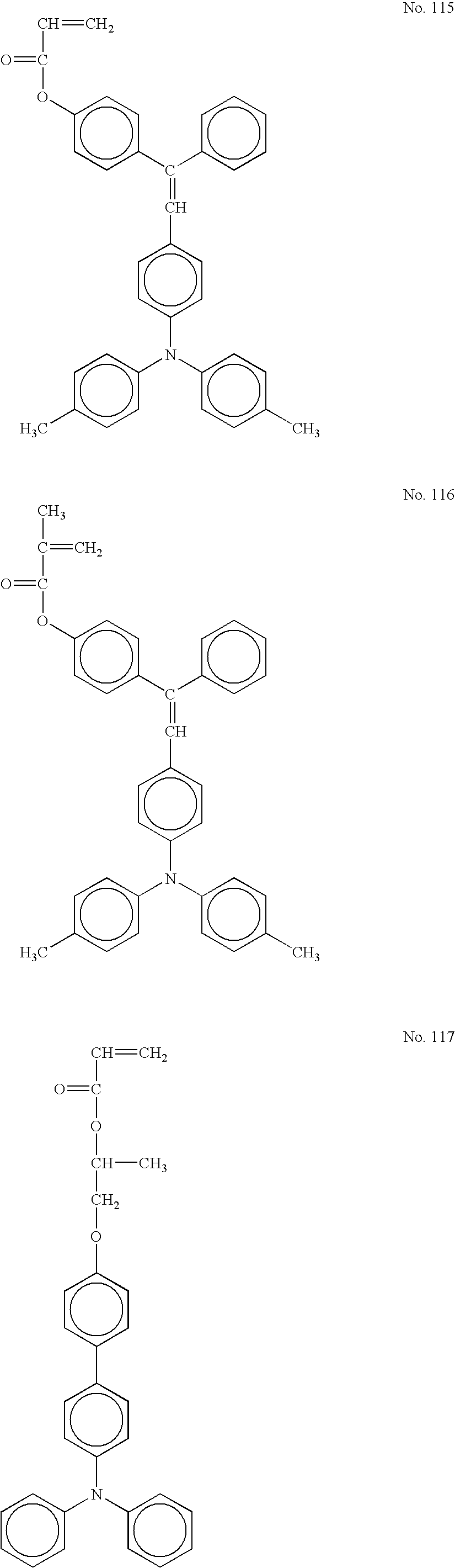


- Also, the one-functional free-radical-polymerizable compound having an electron transporting structure used for the present invention is important for giving charge transportation ability to the cross-linked surface layer and the content of the compound is 20-80% by weight, preferably 30 -70% by weight of the total weight of the cross-linked surface layer. If the content is less then 20% by weight, the charge transportation performance of the cross-linked surface layer cannot be maintained sufficiently and the degradation of the electrical characteristics such as lowering in the sensitivity and the elevation of the residual potential are caused in repeated use. On the other hand, if the content is over 80% by weight, the content of the free-radical-polymerizable monomer having no electron transporting structure represented by general formula (A) is reduced. As the result, the lowering in the cross-link density is caused so that the abrasive resistance is insufficient. As the balance of the electrical characteristics and the abrasive resistance is considered, the content of the compound is most preferably in a range of 30-70% by weight, although it depends on used processes that may require different electrical characteristics or abrasive resistance.
- The surface layer in the present invention is a cross-linked surface layer obtained by simultaneously curing at least the free-radical-polymerizable monomer having no electron transporting structure represented by general formula (A) and the one-functional free-radical-polymerizable compound having an electron transporting structure. Herein, a one-through four-functional free-radical-polymerizable monomer and a radical-polymerizable oligomer can be used in combination for the purpose of giving a function such as the control of the viscosity of a coating liquid for the surface layer, stress relaxation for the cross-linked surface layer, the reduction of surface free energy, and the reduction of a friction coefficient.
- A well-known free-radical-polymerizable monomer and a well-known oligomer can be used.
- As the one-through four-functional free-radical-polymerizable monomer, the following compounds are exemplified but the monomer is not limited to these compounds.
- That is, as the free-radical-polymerizable monomer used in the present invention, for example, trimethylolpropane triacrylate (TMPTA), trimethylolpropane trimethacrylate, HPA-modified trimethylolpropane triacrylate, EO-modified trimethylolpropane triacrylate, PO-modified trimethylolpropane triacrylate, caprolactone-modified trimethylolpropane triacrylate, HPA-modified trimethylolpropane trimethacrylate, penta-erythritol triacrylate, penta-erythritol tetraacrylate (PETTA), glycerole triacrylate, ECH-modified glycerole triacrylate, EO-modified glycerole triacrylate, PO-modified glycerole triacrylate, tris(acryloxyethyl)isocyanurate, alkyl-modified di-penta-erythritol tetraacrylate, alkyl-modified di-penta-erythritol triacrylate, dimethylolpropane tetraacrylate (DTMPTA), penta-erythritol ethoxytetraacrylate, EO-modified phosphate triacrylate, 2,2,5,5-tetrahydroxymethylcyclopentanone tetraacrylate, 2-ethylhexyl acrylate, 2-hydroxyethyl acrylate, 2-hydroxypropyl acrylate, tetrahydrofurfuryl acrylate, 2-ethylhexylCarbitol acrylate, 3-methoxybutyl acrylate, benzyl acrylate, cyclohexyl acrylate, isoamyl acrylate, isobutyl acrylate, methoxytriethylene glycol acrylate, phenoxytetraethylene glycol acrylate, cetyl acrylate, isostearyl acrylate, stearyl acrylate, styrene monomer, 1,3-butanediol diacrylate, 1,4-butanediol diacrylate, 1,4-butanediol dimethacrylate, 1,6-hexanediol diacrylate, 1,6-hexanediol dimethacrylate, diethyleneglycol diacrylate, neopentylglycol diacrylate, EO-modified bisphenol A diacrylate, EO-modified bisphenol F diacrylate, neopentylglycol diacrylate, di-penta-erythritol pentaacrylate, di-penta-erythritol hexaacrylate, and caprolactone-modified di-penta-erythritol hexaacrylate can be provided.
- As the functional monomer, for example, a reactive additive having a fluorine atom as a substituent or a radical-polymerizable functional group such as octafluoropentyl acrylate, 2-perfluorooctylethyl acrylate, 2-perfluorooctylethyl methacrylate, and 2-perfluoroisononylethyl acrylate and a reactive silicone-based additive such as PO-modified 2-neopentylglycol diacrylate can be effectively used.
- The functional monomers may be used singularly or in combination as a mixture. The content of the functional monomer is 0.01-30% by weight, preferably 0.05-20% by weight of a solid content of coating liquid for forming a cross-linked layer.
- As the radical-polymerizable oligomer, for example, epoxyacrylate-type oligomer, urethane acrylate-type oligomer, and polyester acrylate-type oligomer can be provided. Herein, if a one-functional or two-functional free-radical-polymerizable monomer or a radical-polymerizable oligomer is much contained, the three-dimensional cross-link density of the cross-linked surface layer substantially lowers so that the lowering in the abrasive resistance is caused. Therefore, the content of the monomer and the oligomer is regulated to be equal to or less than 150 parts by weight, preferably equal to or less than 100 parts by weight per 100 parts by weight of the free-radical-polymerizable monomer having no electron transporting structure represented by general formula (A).
- Also, although the surface layer in the present invention is a cross-linked surface layer obtained by simultaneously curing at least the free-radical-polymerizable monomer having no electron transporting structure represented by general formula (A) and the one-functional free-radical-polymerizable compound having an electron transporting structure, a polymerization initiator may be used for the cross-linked surface layer according to need, for example, for promoting the cross-linking reaction efficiently.
- As a thermal polymerization initiator, peroxide-type initiators such as 2,5-dimethylhexane-2,5-dihydroperoxide, dicumylperoxide, benzoyl peroxide, t-butylcumylperoxide, 2,5-dimethyl-2,5-di(peroxybenzoyl)hexyne-3,3-di-t-butylperoxide, t-butylhydroperoxide, cumene hydroperoxide, and lauroyl peroxide, and azoic initiators such as azobis(isobutylnitrile), azobis(cyclohexanecarbonitrile), azobis(methyl isobutyrate), azobis(isobutylamidine hydrochloride), and 4,4′-azobis(4-cyanovaleric acid) can be provided.
- As a photo-polymerization initiator, acetophenone-based or ketal-type photo-polymerization initiators such as diethoxyacetophenone, 2,2-dimethoxy-1,2-diphenylthene-1-one, 1-hydroxycyclohexyl-phenylketone, 4-(2-hydroxyethoxy)phenyl(2-hydroxy-2-propyl)ketone, 2-benzyl-2-dimethylamino-1-(4-morpholinophenyl)butanone-1,2-hydroxy-2-methyl-1-phenylpropane-1-one, 2-methyl-2-morpholino(4-methylthiophenyl)propane-1-one, and 1-phenyl-1,2-propanedione-2-(o-ethoxycarbonyl)oxime, benzoin ether-type photo-polymerization initiators such as benzoin, benzoin methyl ether, benzoin ethyl ether, benzoin isobutyl ether, and benzoin isopropyl ether, benzophenone-based photo-polymerization initiators such as benzophenone, 4-hydroxybenzophenone, methyl o-benzoylbenzoate, 2-benzoylnaphthalene, 4-benzoylbiphenyl, 4-benzoyl phenyl ether, acrylated benzophenone, and 1,4-benzoylbenzene, thioxanthone-based photo-polymerization initiators such as 2-isopropylthioxanthone, 2-chlorothioxanthone, 2,4 -dimethylthioxanthone, 2,4-diethylthioxanthone, and 2,4-dichlorothioxanthone, and other photo-polymerization initiators such as ethylanthraquinone, 2,4,6-trimethylbenzoyldiphenylphosphine oxide, 2,4,6-trimethylbenzoylphenylethoxyphosphine oxide, bis(2,4,6-trimethylbenzoyl)phenylphosphine oxide, bis(2,4-dimethoxybenzoyl)-2,4,4-trimethylpentylphosphine oxide, methylphenylglyoxy ester, 9,10-phenanthrene, acridine-based compounds, triazine-based compounds, and imidazole-based compounds, can be provided.
- Also, additives having photo-polymerization promoting effect can be employed singularly or in combination with the photo-polymerization initiator. For example, triethanolamine, methyldiethanolamine, ethyl 4-dimethylaminobenzoate, isoamyl 4-dimethylaminonemzoate, (2-dimethylamino)ethyl benzoate, and 4,4′-dimethylaminobenzophenone can be provided.
- The polymerization initiators may be used singularly or in combination as a mixture. The content of the polymerization initiator is 0.5-40 parts by weight, preferably 1-20 parts by weight per 100 parts by weight of total contents having a radical polymerizing property.
- Although the surface layer in the present invention is a cross-linked surface layer obtained by simultaneously curing at least the free-radical-polymerizable monomer having no electron transporting structure represented by general formula (A) and the one-functional free-radical-polymerizable compound having an electron transporting structure, filler particles can be contained for the purpose of improving the abrasive resistance.
- The average primary particle size of the filler is preferably 0.01-0.5 μm on the points of light transmittance of the surface layer and the abrasive resistance. If the average primary particle size of the filler is less than 0.01 μm, the degradation of the dispersiveness of the filler is caused and the effect of improving the abrasive resistance is not sufficiently exerted. On the other hand, if the average primary particle size of the filler is over 0.5 μm, the precipitation of the filler may be promoted in a liquid dispersion and toner filming may be caused.
- The higher the concentration of the filler material in the surface layer is, the abrasive resistance is advantageously high. However, if the concentration is too high, a side effect such as the elevation of the residual potential and the reduction of the transmittance of writing light through the surface layer may be caused. Therefore, the concentration is generally equal to or less than 50% by weight, preferably equal to or less than 30% by weight of total solid content.
- Furthermore, the filler can be surface-treated by using at least one kind of surface treatments and such surface treatment is preferable with respect to the dispersiveness of the filler. The reduction of the dispesiveness of the filler does not only cause the elevation of the residual potential but also the reduction of the transparency of a coated film, the generation of defects on a coated film, and further the reduction of the abrasive resistance, which may cause the serious problem of disturbing the attainment of high durability and high quality image.
- As the surface treatment, although all conventionally used surface treatments can be used, a surface treatment capable of keeping the insulation properties of the filler is preferable.
- The amount of the surface treatment is suitably 3-30% by weight, preferably 5-20% by weight of the weight of filler although it depends on the primary particle size of the used filler. If the amount of the surface treatment is less than 3% by weight, the effect of the dispersion of the filler cannot be obtained. Also, if the amount of the surface treatment is over 30% by weight, significant elevation of the residual potential is caused. The filler materials are used singularly or in combination as a mixture.
- Moreover, coating liquid used for the present invention can contain an additive such as each kind of plasticizer (for the purpose of stress relaxation or the improvement of adhesive properties) and a leveling agent according to need. For such additives, well-known additives is can be used. As the plasticizer, a plasticizer generally used for resin, such as dibutyl phthalate, dioctyl phthalate, etc. can be used and the usage of the plasticizer is equal to or less than 20% by weight, preferably equal to or less than 10% by weight of total solid content contained in coating liquid. Also, as the leveling agent, silicone oils such as dimethylsilicone oil, methylphenylsilicone oil, etc. and a polymer or oligomer that contain a perfluoroalkyl group in a side chain thereof can be used and the usage of the leveling agent is appropriately equal to or less than 3% by weight of total solid content contained in coating liquid.
- For a composition contained in coating liquid for cross-linked surface layer, a binder resin can be contained in a quantity such that surface smoothness, electrical characteristics, or durability of the photoconductor are preserved. However, when a polymer material such as a binder resin is contained in coating liquid, phase separation occurs due to the low compatibility with a polymer produced by the curing reaction of a radical-polymerizable composition (the free-radical-polymerizable monomer and the free-radical-polymerizable compound having an electron transporting structure) and, as the result, the irregularity of the surface of the cross-linked surface layer become markedly uneven. Accordingly, no use of a binder resin is preferable.
- The cross-linked surface layer of the present invention is formed by coating and curing coating liquid that contains the free-radical-polymerizable monomer having no electron transporting structure represented by general formula (A) and the one-functional free-radical-polymerizable compound having an electron transporting structure.
- If the free-radical-polymerizable monomer is in a liquid state, such coating liquid in which another component can be dissolved can be coated but coating liquid diluted with solvent according to need is coated. As the used solvent, alcohols such as methanol, ethanol, propanol, and butanol, ketones such as acetone, ethyl methyl ketone, isobutyl methyl ketone, and cyclohexanone, esters such as ethyl acetate and butyl acetate, ethers such as tetrahydrofuran, dioxane, propylether, halogenated hydrocarbons such as dichloromethane, dichloroethane, trichloroethane, and chlorobenzene, aromatic hydrocarbons such as benzene, toluene, and xylene, and cellosolves such as methylcellosolve, ethylcellosolve, and cellosolve acetate can be provided.
- The solvents are used singularly or in combination as a mixture. The dilution ratio of the coating liquid with the solvent is arbitrary decided dependent on the solubility of the composition, a coating method, and objective film thickness. The coating can be carried out using a dip coating method, a spray coat method, a bead coat method, or a ring coat method.
- In the present invention, after such coating liquid is coated, the coated liquid is cured providing external energy, so as to form the cross-linked surface layer. As the external energy, thermal energy, light energy, and radiation energy can be used.
- As a method for applying the thermal energy, the coated liquid is heated from the side of a coated surface or a support using air, a gas such as nitrogen, a vapor, each kind of thermal medium, infrared rays, or electromagnetic waves. The heating temperature is preferably equal to or greater than 100° C. and equal to or less than 170° C. If the temperature is less than 100° C., the reaction rate of curing is slow so that the reaction does not complete perfectly. If the temperature is over 170° C., the reaction promotes inhomogeneously, so that marked distortion occurs in the cross-linked surface layer. In order to promote the curing reaction homogeneously, a method of heating at a comparatively low temperature less than 100° C. and subsequently heating up to a temperature equal to or greater then 100° C. so as to complete the reaction is useful.
- For providing the light energy, an UV light source such as a high-pressure mercury-vapor lamp and a metal halide lamp, which having emission wavelength mainly in a ultraviolet region can be used but a visible light source may be selected in accordance with absorption wavelength of the radical-polymerizable content or photo-polymerization initiator. The illuminance of irradiating light is preferably equal to or greater than 50 mW/cm2 and equal to or less than 1,000 mW/cm2. If the illuminance is less than 50 mW/cm2, it takes a long time to complete the curing reaction. If the illuminance is over 1,000 mW/cm2, the reaction promotes inhomogeneously, so that the irregularity of the cross-linked surface layer is enhanced.
- For providing the radiation energy, an electron beam can be used.
- Among the aforementioned energies, it is useful to employ thermal or light energy because of easy control of the reaction rate and the simplicity of a device.
- Since the film thickness of the cross-linked surface layer used for the present invention depends on the layer structure of the photoconductor in which the cross-linked surface layer is employed, the film thickness is explained with a description of the layer structure below.
- Now, the layer structure of the photoconductor according to the present invention is described below.
- Layer Structure of an Electrophotographic Photoconductor
- An electrophotographic photocondctor according to the present invention is illustrated based on the drawings.
-
FIGS. 1A and 1B illustrate electrophotographic photocondctors having a single layer structure according to the present invention, in which a photoconductive layer having both a charge generation function and a charge transportation function is provided on an electrically conductive support.FIG. 1A illustrates a cross-linked surface layer obtained by cross-linking or curing the entire photoconductive layer andFIG. 1B illustrates a cross-linked surface layer provided on the surface of a photoconductive layer. -
FIGS. 2A and 2B illustrate electrophotographic photocondctors having a laminated layer structure according to the present invention, in which a charge generation layer having a charge generation function and a charge transportation layer having a charge transportation function are laminated on an electrically conductive support.FIG. 2A illustrates a cross-linked surface layer obtained by cross-linking or curing the entire charge transportation layer andFIG. 2B illustrates a cross-linked surface layer provided on the surface of a charge transportation layer. - Electrically Conductive Support
- As the electrically conductive support, an electrically conductive support obtained by applying a film-shaped or cylindrical plastic or paper with an electrically conductive material with a volumetric resistivity of 1010 Ωcm, for example, a metal such as aluminum, nickel, chromium, nichrome, copper, gold, silver, and platinum, and a metal oxide such as tin oxide and indium oxide by means of vapor-depositing or sputtering, a electrically conductive plate made of aluminum, aluminum alloy, nickel, or stainless, and an electrically conductive pipe produced by applying surface treatment such as cutting, super finishing, and polishing to an unfinished pipe obtained by extruding or drawing aluminum, aluminum alloy, nickel, or stainless can be used. Furthermore, an endless nickel belt and an endless stainless belt that are disclosed in Japanese Laid-Open Patent Application No. 52-36016 can be used as the electrically conductive support. Moreover, an electrically conductive support obtained by applying a liquid dispersion containing electrically conductive powder in a proper binder resin on the aforementioned electrically conductive support can be also used.
- As the electrically conductive powder, carbon black powder, acetylene black powder, metal powders such as aluminum powder, nickel powder, iron powder, nichrome powder, copper powder, zinc powder, and silver powder, and metal oxide powders such as electrically conductive tin oxide powder and ITO (indium tin oxide) powder.
- As the binder material used with the electrically conductive powder, a thermoplastic resin, a thermosetting resin, and a photosetting resin, such as poly(styrene), styrene-acrylonitrile copolymer, styrene-butadiene copolymer, styrene-maleic anhydride copolymer, polyester, poly(vinyl chloride), vinyl chloride-vinyl acetate copolymer, poly(vinyl acetate), poly(vinylidene chloride), polyallylate resin, phenoxy resin, polycarbonate, cellulose acetate resin, ethylcellulose resin, poly(vinyl butyral), poly(vinyl formal), poly(vinyltoluene), poly(N-vinylcarbazole), acrylic resin, silicone resin, epoxy resin, melamine resin, urethane resin, phenol resin, and alkyd resin can be provided. Such electrically conductive layer can be provided by applying the dispersion liquid obtained by dispersing the electrically conductive powder and the binder resin in a proper solvent such as tetrahydrofuran, dichloromethane, ethyl methyl ketone, and toluene, onto the aforementioned electrically conductive support.
- Advantageously, the electrically conductive support used for the present invention may be an electrically conductive support obtained by providing an electrically conductive layer made of a heat-shrinkable tubing that contains the aforementioned electrically conductive powder in a material such as poly(vinyl chloride), poly(propylene), polyester, poly(styrene), poly(vinylidene chloride), poly(ethylene), chlorinated rubber, and Teflon (Trade Mark) on a proper cylindrical substrate.
- Photoconductive Layer
- Next, a photoconductive layer is described. The photoconductive layer may have either the laminated structure or the single layer structure.
- A photoconductive layer having the laminated structure includes a charge generation layer having a charge generation function and a charge transportation layer having a charge transportation function. On the other hand, a photoconductive layer having the single layer structure is a layer having both a charge generation function and a charge transportation function.
- Both the laminated-layer-structure photoconductive layer and the single-layer-structure photoconductive layer are described below.
- Laminated-Layer-Structure Photoconductive Layer
- (Charge Generation Layer)
- A charge generation layer is a layer based on a charge generation material having a charge generation function, for which a binder resin can be used in combination according to need.
- As the charge generation material, either an inorganic charge generation material or an organic charge generation material can be employed.
- As the inorganic charge generation material, crystalline selenium, amorphous selenium, selenium-tellurium, a selenium-tellurium-halogen, a selenium-arsenic compound, and amorphous silicon can be provided. Advantageously, the dangling bond of the amorphous silicon may be terminated with a hydrogen atom or a halogen atom and the amorphous silicon may be doped with a boron atom, phosphorus atom, or the like.
- On the other hand, as the organic charge generation material, well-known materials can be used. For example, a phthalocyanine-based pigment such as metal phthalocyanine and an azo pigment containing a triphenylamine skeleton, no-metal phthalocyanine, an azulenium salt pigment, a methyl squarate pigment, an azo pigment containing a carbazole skeleton, an azo pigment containing a triphenylamine skeleton, an azo pigment containing a diphenylamine skeleton, an azo pigment containing a dibenzothiophene skeleton, an azo pigment containing a fluorenone skeleton, an azo pigment containing an oxadiazole skeleton, an azo pigment containing a bis(stilbene) skeleton, an azo pigment containing an distyryloxadiazole skeleton, an azo pigment containing an distyrylcarbazole skeleton, a perylene-based pigment, a polycyclic quinone-based pigment such as an anthraquinone-based pigment, a quinoneimine-based pigment, a diphenylmethane-based pigment, a triphenylmethane-based pigement, a benzoquinone-based pigment, a naphthoquinone-based pigment, a cyanine-based pigment, an azomethyne-based pigment, an indigoid-based pigment, and a bis(benzimidazole)-based pigment can be provided.
- The charge generation materials can be used singularly or in combination as a mixture.
- As the binder resin used for the charge generation layer according to need, polyamide, polyurethane, epoxy resin, polyketone, polycarbonate, silicone resin, acrylic resin, poly(vinyl butyral), poly(vinyl formal), poly(vinyl ketone), polystyrene, poly(N-vinylcarbazole), and polyacrylamide can be provided. The binder resins can be used singularly or in combination as a mixture.
- In addition, as a binder resin for the charge generation layer, beside the aforementioned binder resin, a polymeric charge transportation material having a charge transportation function, for example, a polymer material such as polycarbonate, polyester, polyurethane, polyether, polysiloxane, and an acrylic resin, and a polymer material conatining a polysilane skeleton, all of which have an arylamine skeleton, a benzidine skeleton, a hydrazone skeleton, a carbazole skeleton, a stilbene skeleton, or a pyrazoline skeleton, can be also used.
- Provided as the specific examples of the former are, for example, polymeric charger transportation materials disclosed in Japanese Laid-Open Patent Application No. 01-001728, Japanese Laid-Open Patent Application No. 01-009964, Japanese Laid-Open Patent Application No. 01-013061, Japanese Laid-Open Patent Application No. 01-019049, Japanese Laid-Open Patent Application No. 01-241559, Japanese Laid-Open Patent Application No. 04-011627, Japanese Laid-Open Patent Application No. 04-175337, Japanese Laid-Open Patent Application No. 04-183719, Japanese Laid-Open Patent Application No. 04-225014, Japanese Laid-Open Patent Application No. 04-230767, Japanese Laid-Open Patent Application No. 04-320420, Japanese Laid-Open Patent Application No. 05-232727, Japanese Laid-Open Patent Application No. 05-310904, Japanese Laid-Open Patent Application No. 06-234836, Japanese Laid-Open Patent Application No. 06-234837, Japanese Laid-Open Patent Application No. 06-234838, Japanese Laid-Open Patent Application No. 06-234839, Japanese Laid-Open Patent Application No. 06-234840, Japanese Laid-Open Patent Application No. 06-234841, Japanese Laid-Open Patent Application No. 06-239049, Japanese Laid-Open Patent Application No. 06-236050, Japanese Laid-Open Patent Application No. 06-236051, Japanese Laid-Open Patent Application No. 06-295077, Japanese Laid-Open Patent Application No. 07-056374, Japanese Laid-Open Patent Application No. 08-176293, Japanese Laid-Open Patent Application No. 08-208820, Japanese Laid-Open Patent Application No. 08-211640, Japanese Laid-Open Patent Application No. 08-253568, Japanese Laid-Open Patent Application No. 08-269183, Japanese Laid-Open Patent Application No. 09-062019, Japanese Laid-Open Patent Application No. 09-043883, Japanese Laid-Open Patent Application No. 09-71642, Japanese Laid-Open Patent Application No. 09-87376, Japanese Laid-Open Patent Application No. 09-104746, Japanese Laid-Open Patent Application No. 09-110974, Japanese Laid-Open Patent Application No. 09-110976, Japanese Laid-Open Patent Application No. 09-157378, Japanese Laid-Open Patent Application No. 09-221544, Japanese Laid-Open Patent Application No. 09-227669, Japanese Laid-Open Patent Application No. 09-235367, Japanese Laid-Open Patent Application No. 09-241369, Japanese Laid-Open Patent Application No. 09-268226, Japanese Laid-Open Patent Application No. 09-272735, Japanese Laid-Open Patent Application No. 09-302084, Japanese Laid-Open Patent Application No. 09-302085, and Japanese Laid-Open Patent Application No. 09-328539.
- Also, provided as the specific examples of the latter are, for example, polysilylenes disclosed in Japanese Laid-Open Patent Application No. 63-285552, Japanese Laid-Open Patent Application No. 05-19497, Japanese Laid-Open Patent Application No. 05-70595, and Japanese Laid-Open Patent Application No. 10-73944.
- Additionally, a low-molecular-weight charge transportation material can be contained in the charge generation layer. As the low-molecular-weight charge transportation material used for the charge generation layer, a hole transportation material and a electron transportation material can be provided.
- As the electron transportation material, an electron accepting material such as chloroanil, bromoanil, tetracyanoethylene, tetracyanoquinodimethane, 2,4,7-trinitro-9-fluorenone, 2,4,5,7-tetranitro-9-fluorenone, 2,4,5,7-tetranitroxanthone, 2,4,8-trinitrothioxanthone, 2,6,8-trinitro-4H-indeno[1,2-b]thiophene-4-one, 1,3,7-trinitrodibenzothiophene-5,5-dioxide, and diphenoquinone derivatives can be provided. The electron transportation materials can be used singularly or in combination as a mixture.
- As the hole transportation material, an electron donating material as described below can be provided and preferably used.
- As the hole transportation material, oxazole derivatives, oxadiaxole derivatives, imidazole derivatives, monoarylamine derivatives, diarylamine derivatives, triarylamine derivatives, stilbene derivatives, α-phenylstilbene derivatives, benzidine derivatives, diarylmethane derivatives, triarylmethane derivatives, 9-styrylanthracene derivatives, pyrazoline derivatives, divinylbenzene derivatives, hydrazone derivatives, indene derivatives, butadiene derivatives, pyrene derivatives, bis(stilbene) derivatives, enamine derivatives, and other well-known materials can be provided. The hole transportation materials can be used singularly or in combination as a mixture.
- As a representative method for forming the charge generation layer, a method of producing a thin film in vacuum and a method of casting from solution or liquid dispersion can be provided.
- As the former method, a vapor deposition method, a glow discharge decomposition method, an ion plating method, a sputtering method, a reactive sputtering method, a CVD method can be provided and a charge generation layer that contains the inorganic charge generation material or the organic charge generation material can be formed well.
- When a charge generation layer is formed by the latter casting method, the charge generation layer can be formed by dispersing the inorganic or organic charge generation material, if necessary, with the binder resin, into a solvent such as tetrahydrofuran, dioxane, dioxoran, toluene, dichloromethane, monochlorobenzene, dichloroethane, cyclohexanone, cyclopentanone, anisole, xylene, ethyl methyl ketone, acetone, ethyl acetate, and butyl acetate, by means of ball-mill, AttrIter, sand mill, or beads mill, then moderately diluting the obtained liquid dispersion and applying the diluted dispersion. Additionally, a leveling agent such as dimethylsilicone oil and methylphenylsilicone oil can be added according to need. Application of coating liquid can be carried out by means of dip coating, spray coating, beads coating, or ring coating.
- The film thickness of the charge generation layer provided as described above is appropriately 0.01-5 μm, preferably 0.05-2 μm.
- (Charge Transportation Layer)
- A charge transportation layer is a layer having a charge transportation function and a cross-linked surface layer having a charge transporting structure is used as the charge transportation layer in the present invention. When the cross-linked surface layer is the whole of a charge transportation layer, as described in the aforementioned method of producing a cross-linked surface layer, the cross-linked surface layer is formed by applying coating liquid that contains a radical-polymerizable composition for the present invention (the radical polymerizable monomer having no charge transporting structure represented by general formula (A) and the one-functional radical-polymerizable compound having a charge transporting structure) onto the charge generation layer, drying the coating liquid according to need, and initiating a curing reaction due to external energy. Herein, the film thickness of the cross-linked surface layer is 10-30 μm, preferably 10-25 μm. If the film thickness is less than 10 μm, a sufficient charging electrical potential cannot be maintained. On the other hand, if the film thickness is over 30 μm, the cross-linked surface layer easily separates from an under layer due to the volume shrinkage at the time of curing.
- When the cross-linked surface layer is formed on the surface of a charge transportation layer, or, in other words, a charge transportation layer has a laminated structure, a charge transportation layer portion, which is an under layer of the cross-linked surface layer, can be formed by dissolving or dispersing a charge transportation material having a charge transportation function and a binder resin into a proper solvent, applying the obtained solution or dispersion liquid onto a charge generation layer and drying the applied solution or dispersion liquid. Subsequently, the coating liquid containing a radical-polymerizable composition for the present invention is applied on the charge transportation layer portion and cross-linked or cured by using external energy so as to obtain a cross-linked surface layer.
- As the charge transportation material, the electron transportation materials, the hole transportation materials, and the polymeric charge transportation materials, described for the charge generation layer, can be used. As described above, the use of the polymeric charge transportation material is particularly useful since the solubility of the under layer portion of the charge transportation layer at the time of applying the coating liquid for the cross-linked surface layer can be reduced.
- As the binder resin used in combination with the charge transportation material, a thermoplastic resin and a thermosetting resin, such as poly(styrene), styrene-acrylonitrile copolymer, styrene-butadiene copolymer, styrene-maleic anhydride copolymer, polyester, poly(vinyl chloride), vinyl chloride-vinyl acetate copolymer, poly(vinyl acetate), poly(vinylidene chloride), polyallylate resin, phenoxy resin, polycarbonate, cellulose acetate resin, ethylcellulose resin, poly(vinyl butyral), poly(vinyl formal), poly(vinyltoluene), poly(N-vinylcarbazole), acrylic resin, silicone resin, epoxy resin, melamine resin, urethane resin, phenol resin, and alkyd resin can be provided.
- The content of the charge transportation material is appropriately 20-300 parts by weight, preferably 40-150 parts by weight per 100 parts by weight of the binder resin. Additionally, when the polymeric charge transportation material is used, the polymeric charge transportation materials can be used singularly or in combination with the binder resin.
- As a solvent used in the coating liquid for the under layer portion of the charge transportation layer, a solvent for the charge generation layer can be similarly used but a solvent that can dissolve the charge transportation material and the binder resin well is preferable. The solvents may be used singularly or in combination as a mixture. Also, in order to form the under layer portion of the charge transportation layer, the coating methods for the charge generation layer can be used similarly.
- Additionally, a plasticizer or a leveling agent can be added according to need. As the palsticizer used for the under layer portion of the charge transportation layer, a plasticizer used for a general resin, such as dibutyl phthalate and dioctyl phthalate, can be directly used and the usage of the plasticizer is appropriately 0-30 parts by weight per 100 parts by weight of the binder resin. As the leveling agent used for the under layer portion of the charge transportation layer, silicone oils such as dimethylsilicone oil and methylphenylsilicone oil and a polymer oligomer containing a perfluoroalkyl group in side chain thereof can be provided and the usage of the leveling agent is appropriately 0-1 parts by weight per 100 parts by weight of the binder resin.
- The film thickness of the under layer portion of the charge transportation layer is approximately 5-40 μm, preferably 10-30 μm.
- When the cross-linked surface layer is a surface portion of charge transportation layer, as described in the aforementioned method of producing a cross-linked surface layer, the cross-linked surface layer is formed by applying the coating liquid that contains a radical-polymerizable composition for the present invention onto the under layer portion of the charge transportation layer, drying the applied coating liquid according to need, and initiating a curing reaction due to external thermal or light energy. In this case, the film thickness of the cross-linked surface layer is 1-20 μm, preferably 2-10 μm. If the film thickness is less than 1 μm, the durability of the cross-linked surface layer is variable dependent on the ununiformity of the film thickness. On the other hand, if the film thickness is over 20 μm, the film thickness of the whole of charge transportation layer becomes large, whereby the diffusion of charges increases and the reproducibility of an image decreases.
- Single-Layer-Structure Photoconductive Layer
- A single-layer-structure photoconductive layer is a layer having both a charge generation function and a charge transportation function. The cross-linked surface layer having a charge transporting structure used for the present invention contains a charge generation material having a charge generation function and is usefully used as a single-layer-structure photoconductive layer. As described in the method for forming the charge generation layer by means of casting, the cross-linked surface layer is formed by dispersing the charge generation material into coating liquid containing the radical-polymerizable composition, applying the coating liquid onto a electrically conductive support, drying the applied coating liquid according to need, and initiating a curing reaction by external energy. Herein, liquid dispersion in which the charge generation material is previously dispersed in a solvent may be added into the coating liquid for cross-linked surface layer.
- In this case, the film thickness of the cross-linked surface layer is 10-30 μm, preferably 10-25 μm. If the film thickness is less than 10 μm, a sufficient charging electrical potential cannot be maintained. On the other hand, if the film thickness is over 30 μm, the cross-linked surface layer easily separates from an electrically conductive substrate or an underlying layer due to the volume shrinkage at the time of curing.
- Also, when the cross-linked surface layer is a surface portion of single-layer-structure photoconductive layer, a photoconductive layer portion, which is an under layer of the cross-linked surface layer, can be formed by dissolving or dispersing a charge generation material having a charge generation function, a charge transportation material having a charge transportation function, and a binder resin into a proper solvent, applying the obtained solution or dispersion liquid onto an electrically conductive support or an underlying layer, and drying the applied solution or dispersion liquid.
- Additionally, a plasticizer and a leveling agent can be added according to need. For the method of dispersing a charge generation material, the charge generation material, the charge transportation material, a plasticizer, and a leveling agent, those provided for the charge generation layer and the charge transportation layer can be similarly used. As the binder resin, beside the binder resin provided for the charge transportation layer, the binder resin provided for the charge generation layer may be used in combination. Also, the aforementioned polymeric charge transportation material can be used and is useful in that mixing of the composition contained in the under layer portion of the photoconductive layer into the cross-linked surface layer can be reduced. The film thickness of the under layer portion of the photoconductive layer is approximately 5-30 μm, preferably 10-25 μm.
- When the cross-linked surface layer is a surface portion of the single-layer-structure photoconductive layer, as described above, the cross-linked surface layer is formed by applying the coating liquid that contains a radical-polymerizable composition for the present invention and the charge generation material onto the under layer portion of the photoconductive layer, drying the applied coating liquid according to need, and curing the dried coating liquid due to external thermal or light energy. In this case, the film thickness of the cross-linked surface layer is 1-20 μm, preferably 2-10 μm. If the film thickness is less than 1 μm, the durability of the cross-linked surface layer is variable dependent on the ununiformity of the film thickness. On the other hand, if the film thickness is over 20 μm, the film thickness of the whole of charge transportation layer becomes large, whereby the diffusion of charges increases and the reproducibility of an image decreases.
- The content of the charge generation material contained in the single-layer-structure photoconductive layer is preferably 1-30% by weight of the total quantity of the photoconductive layer. Also, the content of the binder resin contained in the under layer portion of the photoconductive layer is preferably 20-80% by weight of the total quantity of the photoconductive layer. Further, the content of the charge transportation material is preferably 10-70% by weight of the total quantity of the photoconductive layer.
- Intermediate Layer
- In the photoconductor according to the present invention, the cross-linked surface layer is a surface portion of photoconductive layer, an intermediate layer can be provided between the cross-linked surface layer and the under layer portion of the photoconductive layer for the purpose of suppressing the contamination of a component of the under layer portion into the cross-linked surface layer or improving the adhesive property to the under layer portion. The intermediate layer prevents the inhibition of the curing reaction and the generation of irregularities of the cross-linked surface layer, which are caused by the contamination of the composition contained in the under layer portion of the photoconductive layer into the outermost surface layer that contains the radical-polymerizable composition. Also, the adhesive property of the cross-linked surface layer to the under layer portion of the photoconductive layer can be improved.
- The intermediate layer is generally based on a binder resin. As such binder resin, polyamide, alcohol-soluble nylon, water-soluble poly(vinyl butyral), poly(vinyl butyral), and poly(vinyl alcohol) can be provided. As a method for forming an intermediate layer, a commonly used coating method is employed as described above. Additionally, the thickness of the intermediate layer is appropriately 0.05-2 μm.
- Underlying Layer
- In the photoconductor according to the present invention, an underlying layer can be provided between the electrically conductive support and the photoconductive layer. Although the underlying layer is generally based on a resin, such resin is desirably a resin having a high solvent resistance against a general organic solvent, considering the application of coating liquid for photoconductive layer in a solvent on the underlying layer. As such resin, a water-soluble resin such as poly(vinyl alcohol), casein, and poly(sodium acrylate), an alcohol-soluble resin such as copolymerized nylon and methoxymethylated nylon, and a curing-type resin in which a three-dimensional network structure such as polyurethane, melamine resin, phenol resin, alkyd-melamine resin, and epoxy resin can be provided. In addition, a fine powder pigment of a metal oxide such as titanium oxide, silica, alumina, zirconium oxide, tin oxide, and indium oxide, may be added into the underlying layer for preventing the generation of a moire pattern and reducing the residual electric potential.
- The underlying layer can be formed be using a proper solvent and a coating method as used for the aforementioned photoconductive layer. Further, a silane coupling agent, titanium coupling agent, chromium coupling agent, etc. can be used for the underlying layer in the present invention. Beside the aforementioned underlying layer, anodized Al2O3, an underlying layer made of an organic material such as poly(para-xylene) (parylene) or an inorganic material such as SiO2, SnO2, TiO2, ITO, and CeO2, by using a method of producing a thin film in vacuum, and a well-known underlying layer can be used well as the underlying layer in the present invention. The thickness of the underlying layer is appropriately 0-5 μm.
- Addition of Antioxidant into Each Layer
- In the present invention, an antioxidant can be added into each layer such as the cross-linked surface layer, the charge generation layer, the charge transportation layer, the underlying layer, and the intermediate layer, for improving an environmental resistance and, particularly, preventing the lowering in the sensitivity and the elevation of the residual electric potential.
- As the antioxidant used for the present invention, the following antioxidants can be provided.
- (Phenol-Based Compounds)
- 2,6-di-t-butyl-p-crezol, butylated hydroxyanisole, 2,6-di-t-butyl-4-ethylphenol, stearyl β-(3,5-di-t-butyl-4-hydroxyphenyl)propionate, 2,2′-methylene-bis(4-methyl-6-t-butylphenol), 2,2′-methylene-bis(4-ethyl-6-t-butylphenol), 4,4′-thiobis(3-methyl-6-t-butylphenol), 4,4′-butylidene-bis(3-methyl-6-t-butylphenol), 1,1,3-tris(2-methyl-4-hydroxy-5-t-butylphenyl)butane, 1,3,5-trimethyl-2,4,6-tris(3,5-di-t-butyl-4-hydroxybenzyl)benzene, tetrakis[methylene-3-(3′,5′-di-t-butyl4′-hydroxyphenyl)propionate]methane, bis[3,3′-bis(4′-hydroxy-3′-t-butylphenyl)butyric acid] glycol ester, tocopherols, etc.
- (Paraphenylenediamines)
- N-phenyl-N′-isopropyl-p-phenylenediamine, N,N′-di-sec-butyl-p-phenylenediamine, N-phenyl-N-sec-butyl-p-phenylenediamine, N,N′-di-isopropyl-p-phenylenediamine, N,N′-dimethyl-N,N′-di-t-butyl-p-phenylenediamine, etc.
- (Hydroquinones)
- 2,5-di-t-octylhydroquinone, 2,6-didodecylhydroquinone, 2-dodecylhydroquinone, 2-dodecyl-5-chlorohydroquinone, 2-t-octyl-5-methylhydroquinone, 2-(2-octadecenyl)-5-methylhydroquinone, etc.
- (Organic Sulfur Compounds)
- dilauryl-3,3′-thiodipropionate, distearyl-3,3′-thiodipropionate, ditetradecyl-3,3′-thiodipropionate, etc.
- (Organic Phosphorus Compounds)
- triphenylphosphine, tri(nonylphenyl)phosphine, tri(dinonylphenyl)phosphine, tricresylphosphine, tri(2,4-dibutylphenoxy)phosphine, etc.
- These compounds are well-known as antioxidants for a rubber, a plastic, a fat and a fatty oil and a commercially available product thereof can be easily obtained.
- In the present invention, the content of the antioxidant is 0.01-10% by weight of the total weight of a layer to which the antioxidant is added.
- Image Formation Method and Apparatus
- Next, an image formation method and an image formation apparatus according to the present invention are illustrated in detail based on the drawings.
- The image formation method and the image formation apparatus according to the present invention involve the use of a photoconductor having a smooth charge-transporting cross-linked surface layer with low surface energy and a process including, generally at least, a charging step, an image-wise light exposure step, and a developing step for the photoconductor, subsequently, a transcription step and a fixing step, which transcribes and fixes a toner image to an image supporter (a transcription paper), respectively, and a cleaning step of cleaning the surface of the photoconductor. However, in an image formation method in which an electrostatic latent mage is directly transcribed onto and developed on a transcription medium, not all steps in the process for the photoconductor is required.
-
FIG. 3 is a schematic diagram showing an example of the image formation apparatus. An electrically charging charger 3 is employed as means for uniformly charging the photoconductor. As the charging means, a corotron device, a scorotron device, a solid discharge device, a needle electrode device, a roller charging device, and an electrically conductive brush device can be employed and well-known charging methods can be used. - Next, an image-wise
light exposure part 5 is employed for forming an electrostatic latent image on the uniformly charged photoconductor 1. As a light source of the image-wiselight exposure part 5, all light emitters such as a fluorescent lamp, a tungsten lamp, a halogen lamp, a mercury vapor lamp, a sodium vapor lamp, a light-emitting diode (LED), a semiconductor laser diode (LD), and an electroluminescent (EL) device can be used. Additionally, in order to irradiate the photoconductor with light of a desired wavelength region, each kind of filters such as a sharp cut filter, a bandpass filter, a near-infrared cut filter, a dichroic filter, an interference filter, and a color conversion filter can be employed. - Next, a
development unit 6 is used for visualizing the electrostatic latent image formed on the photoconductor 1. As a development method, a one-component development method and a two-component development method, which use dry-type toner, and a wet-process development method, which uses wet-type toner, can be provided. When positive (negative) charging is applied on the photoconductor and image-wise light exposure is performed, a positive (negative) electrostatic latent image is formed on the surface of the photoconductor. When the electrostatic latent image is developed with negatively (positively)—charged toner (charge detecting fine particles), a positive image can be obtained. On the contrary, when the electrostatic latent image is developed with positively (negatively)—charged toner, a negative image can be obtained. - Next, a
transcription charger 10 is used for transcribing the visualized toner image on the photoconductor to atranscription medium 9. In addition, apre-transcription charger 7 may be used in order to perform better transcription. As the transcription means, electrostatic transcription means such as a transcription charger and a bias roller, mechanical transcription means such as adhesion transcription means and pressure transcription means, and magnetic transcription means can be used. As the electrostatic transcription means, the aforementioned charging means can be also used. - Next, as means for separating the
transcription medium 9 from the photoconductor 1, aseparation charger 11 and aseparation claw 12 can be used. As other separation means, a electrostatic adsorption induced separation means, side end belt separation means, a tip grip conveyor, and curvature separation means can be used. As theseparation charger 11, the aforementioned charging means can be also used. - Next, a
fur brush 14 and acleaning blade 15 can be used for cleaning the photoconductor after the transcription on which the toner remains. In addition, apre-cleaning charger 13 can be employed in order to perform more efficient cleaning. As other cleaning means, web cleaning means and magnetic brush means can be used. The cleaning means can be used singularly or in combination. - Next, a charge elimination means may be used for eliminating the latent image remaining on the photoconductor according to need. As the charge elimination means, a charge elimination lamp 2 and a charge elimination charger can be used, and the aforementioned light source for light exposure and the aforementioned charging means can be used, respectively.
- Furthermore, as original copy reading means, paper feeding means, fixing means, and paper delivering means, which are not adjacent to the photoconductor, well-known means can be used, respectively.
- The image formation method and the image formation apparatus according to the present invention use the electrophotographic photoconductor according to the present invention in an image formation means as mentioned above.
- The image formation means may be incorporated and fixed in a copying machine, a facsimile machine, or a printer. However, the image formation machine may be incorporated in the aforementioned apparatus as a process cartridge, which are detachable from the main body of the apparatus. An example of the process cartridge is shown in
FIG. 4 . - A process cartridge for image formation apparatus incorporates a
photoconductor 101, and at least one of charging means 102, developing means 104, transcription means 106, cleaning means 107, and charge elimination means (not shown in the drawings) and a unit (a component) that is detachable from the main body of an image formation apparatus. - In an image formation process using a unit illustrated in
FIG. 4 , thephotoconductor 101 rotates along a direction denoted by an arrow and an electrostatic latent image is formed on the surface of the photoconductor by charging with charging means 102 and light exposure with light exposure means 103, which electrostatic latent image corresponds to a light exposure image. The electrostatic latent image is developed by the develop means 104 and the toner-developed image is transcribed onto atranscription medium 105 by using transcription means 106 and printed out. Then, the surface of the photoconductor after the image transcription is cleaned by cleaning means 107 and is charge-eliminated by charge elimination means (not shown in the drawings). Again, the process as described above is repeated. - The present invention also provides a process cartridge for image formation apparatus, in which a photoconductor having a polymeric charge transportation layer and the aforementioned cross-linked surface layer and at least one of charging means, developing means, transcription means, cleaning means, and charge elimination means are integrated.
- As apparent from the above description, an electrophotographic photoconductor according to the present invention are not only utilized in an electrophotographic copying machine but also can be widely used in the field of an electrophotograhic application such as a laser beam printer, a CRT printer, a LED printer, a liquid crystal printer and a laser plate making.
- Synthesis Example of a One-Functional Free-Radical-Polymerizable Compound Having Electron Transporting Structure
- For example, a one-functional free-radical-polymerizable compound having an electron transporting structure in the present invention can be synthesized by a method disclosed in Japanese Patent No. 3164426, one example of which is described below.
- (1) The synthesis of a hydroxyl-group-substituted triarylamine compound (represented by the following structural formula B).
- 240 ml of sulfolane was added into 113.85 g (0.3 mol) of a methoxy-group-substituted triarylamine compound (represented by the following structural formula A) and 138 g (0.92 mol) of sodium iodide and the mixture was heated to 60° C. in nitrogen stream. 99 g (0.91 mol) of chlorotrimethylsilane was dropped into the liquid for 1 hour and stirring for 4 and half hours was performed at the temperature of approximately 60° C. to complete the reaction. Approximately 1.5 L of toluene was added into the reaction liquid, which was cooled to the room temperature and washed with water or an aqueous solution of sodium carbonate repeatedly. Then, solvent was removed from the toluene solution and the purification by a column chromatographic treatment (adhesion medium; silica gel, developing solvent; toluene:ethyl acetate=20:1) was carried out. Cyclohexane was added into the obtained pale-yellow oil so as to precipitate a crystal. Thus, 88.1 g (yield=80.4%) of a white crystal represented by the following structural formula B was obtained.
- Melting point: 64.0° C.-66.0° C.
TABLE 1 Results of elemental analysis (%) C H N Found value 85.06 6.41 3.73 Calculated value 85.44 6.34 3.83 Structural formula A 
Structural formula B 
- (2) Triarylamino-group-substituted acrylate compound (illustrated compound No. 54)
- 82.9 g (0.227 mol) of the hydroxyl-group-substituted triarylamine compound (structural formula B) obtained in (1) was dissolved in 400 ml of tetrahydrofuran and an aqueous solution of sodium hydroxide (NaOH: 12.4 g, water: 100 ml) was dropped into the terahydrofuran solution in nitrogen stream. The obtained solution was cooled to 5° C. and 25.2 g (0.272 mol) of acryloyl chloride was dropped into the solution for 40 minutes. Then, stirring for 3 hours was performed at 5° C. to complete the reaction. Water was poured into the reaction liquid and extraction with toluene was performed. The extracted liquid was washed with an aqueous solution of sodium bicarbonate or water repeatedly. Then, solvent was removed from the toluene solution and the purification by a column chromatographic treatment (adhesion medium; silica gel, developing solvent; toluene) was carried out. n-hexane was added into the obtained colorless oil so as to precipitate a crystal. Thus, 80.73 g (yield=84.8%) of a white crystal of illustrated compound No. 54 was obtained.
- Melting point: 117.5° C.-119.0° C.
TABLE 2 Results of elemental analysis (%) C H N Found value 83.13 6.01 3.16 Calculated value 83.02 6.00 3.33 - Next, the present invention is further explained by examples in detail but the present invention is not limited to the following examples. Herein, all “part” used in the examples mean “part by weight”.
- Coating liquid for underlying layer, coating liquid for charge generation layer, and coating liquid for charge transportation layer, which had the following compositions, were applied on an aluminum cylinder in the order by dip coating and dried so as to form 3.5 μm of an underlying layer, 0.2 μm of an charge generation layer, and 23 μm of an charge transportation layer.
- {Coating Liquid for Underlying Layer}
- Alkyd resin: 6 parts
- (Beckosol 1307-60-EL produced by DAINIPPON INK AND CHEMICALS, INCORPORATED)
- Melamine resin: 4 parts
- (Superbeckamine G-821-60 produced by DAINIPPON INK AND CHEMICALS, INCORPORATED)
- Titanium oxide: 40 parts
- (CR-EL: ISHIHARA SANGYO KAISHA, LTD.)
- Ethyl methyl ketone: 50 parts
- {Coating Liquid for Charge Generation Layer}
- Bisazo pigment having the following structure: 2.5 parts

- Polyvinyl butyral: 0.5 parts
- (XYHL produced by UCC)
- Cyclohexanone: 200 parts
- Ethyl methyl ketone: 80 parts
- {Coating Liquid for Charge Transportation Layer}
- Bisphenol Z-typed polycarbonate: 10 parts
- (Panlite TS-2050 produced by TEIJIN CHEMICALS LTD.)
- Low-molecular-weight charge transportation material having the following structure: 7 parts

- Tetrahydrofuran: 100 parts
- Tetrahydrofuran solution of 1% silicone oil: 1 part
- (KF50-100CS produced by Shin-Etsu Chemical Co., Ltd.)
- Coating liquid for cross-linked surface layer having the following composition was spray-coated on the charge transportation layer. Light irradiation was carried out by using a metal halide lamp under the condition of irradiation intensity of 500 mW/cm2 and irradiation time of 20 seconds. Further, drying at 130° C. for 30 minutes was applied so as to provide 4.0 μm of a cross-linked surface layer, so that an electrophotographic photoconductor according to the present invention was obtained.
- {Coating Liquid for Cross-Linked Surface Layer}
- Free-radical-polymerizable monomers having no electron transporting structure: 95 parts
- Di-penta-erythritol hexaacrylate
- (a mixture with pentaacrylate based on hexaacrylate; KAYARAD DPHA produced by NIPPON KAYAKU CO., LTD.)

- (wherein a=5 and b=1 or a=6 and b=0.)
- One-functional free-radical-polymerizable compound having an electron transporting structure: 95 parts
- (Illustrated Compound No. 54)
- Photo-polymerization initiator: 10 parts
- 1-hydroxy-cyclohexyl phenyl ketone
- (Irgacure 184 produced by Ciba Specialty Chemicals)
- Tetrahydrofuran: 1200 parts
- An electrophotographic photoconductor was produced similar to example 1-1 except that the free-radical-polymerizable monomer having no electron transporting structure contained in the coating liquid for cross-linked surface layer in example 1-1 was changed to the following compound.
- Caprolactone-modifieddi-penta-erythritol hexaacrylate
- (KAYARAD DPCA-60 produced by NIPPON KAYAKU CO., LTD.)

- An electrophotographic photoconductor was produced similar to example 1-1 except that the free-radical-polymerizable monomer having no electron transporting structure contained in the coating liquid for cross-linked surface layer in example 1-1 was changed to the following compound.
- EO-modified di-penta-erythritol hexaacrylate
- (KAYARAD DPEA-12 produced by NIPPON KAYAKU CO., LTD.)

- (Herein, the mean average of n is 12.)
- An electrophotographic photoconductor was produced similar to example 1-1 except that the free-radical-polymerizable monomer having no electron transporting structure contained in the coating liquid for cross-linked surface layer in example 1-1 was changed to the following compound.
- Free-radical-polymerizable monomer having no electron transporting structure: 95 parts
- (1) Caprolactone-modified di-penta-erythritol hexaacrylate: 47.5 parts
- (KAYARAD DPCA-120 produced by NIPPON KAYAKU CO., LTD.)

- (2) Trimethylol propane triacrylate: 47.5 parts
- (TMPTA produced by Tokyo Kasei Kogyo Co., Ltd.)

- An electrophotographic photoconductor was produced similar to example 1-1 except that the free-radical-polymerizable monomer having no electron transporting structure contained in the coating liquid for cross-linked surface layer in example 1-1 was changed to the following compound.
- Free-radical-polymerizable monomer having no electron transporting structure: 95 parts
- (1) Di-penta-erythritol hexaacrylate: 47.5 parts
- (a mixture with pentaacrylate based on hexaacrylate; KAYARAD DPHA produced by NIPPON KAYAKU CO., LTD.)

- (wherein a=5 and b=1 or a=6 and b=0.)
- (2) Trimethylol propane triacrylate: 47.5 parts
- (TMPTA produced by Tokyo Kasei Kogyo Co., Ltd.)

- An electrophotographic photoconductor was produced similar to example 1-1 except that the free-radical-polymerizable monomer having no electron transporting structure contained in the coating liquid for cross-linked surface layer in example 1-1 was changed to the following compound.
- Free-radical-polymerizable monomer having no electron transporting structure: 95 parts
- (1) Di-penta-erythritol hexaacrylate: 47.5 parts
- (A mixture with pentaacrylate based on hexaacrylate; KAYARAD DPHA produced by NIPPON KAYAKU CO., LTD.)

- (wherein a=5 and b=1 or a=6 and b=0.)
- (2) Caprolactone-modified di-penta-erythritol hexaacrylate: 47.5 parts
- (KAYARAD DPCA-120 produced by NIPPON KAYAKU CO., LTD.)

- An electrophotographic photoconductor was produced similar to example 1-1 except that the free-radical-polymerizable compound having an electron transporting structure contained in the coating liquid for cross-linked surface layer in example 1-1 was changed to illustrated compound No. 16.
- An electrophotographic photoconductor was produced similar to example 1-1 except that the free-radical-polymerizable compound having an electron transporting structure contained in the coating liquid for cross-linked surface layer in example 1-1 was changed to illustrated compound No. 24.
- An electrophotographic photoconductor was produced similar to example 1-1 except that the coating liquid for cross-linked surface layer in example 1-1 was changed to the following liquid.
- {Coating Liquid for Cross-Linked Surface Layer}
- Free-radical-polymerizable monomer having no electron transporting structure: 90 parts
- Caprolactone-modified di-penta-erythritol hexaacrylate
- (KAYARAD DPCA-120 produced by NIPPON KAYAKU CO., LTD.)

- One-functional free-radical-polymerizable compound having an electron transporting structure: 90 parts
- (Illustrated Compound No. 54)
- Photo-polymerization initiator: 20 parts
- 1-hydroxy-cyclohexyl phenyl ketone
- (Irgacure 184 produced by Ciba Specialty Chemicals)
- Tetrahydrofuran: 90 parts
- Filler fine particles: 20 parts
- Alumina filler (AA03 produced by SUMITOMO CHEMICAL CO., LTD.)
- (Comparison 1-1)
- An electrophotographic photoconductor was produced similar to example 1-1 except that the free-radical-polymerizable monomer having no electron transporting structure in example 1-1 was not added.
- (Comparison 1-2)
- An electrophotographic photoconductor was produced similar to example 1-1 except that the free-radical-polymerizable monomer having no electron transporting structure contained in the coating liquid for cross-linked surface layer in example 1-1 was changed to the following material.
- Free-radical-polymerizable monomer having no electron transporting structure represented by the following structural formula: 95 parts

- Two-functional acrylate: KAYARAD NPGDA produced by NIPPON KAYAKU CO., LTD.
- Molecular weight: 212
- Number of functional groups: two-functionality
- Molecular weight/Number of
functional groups 106 - (Comparison 1-3)
- An electrophotographic photoconductor was produced similar to example 1-1 except that the one-functional free-radical-polymerizable compound having an electron transporting structure contained in the coating liquid for cross-linked surface layer in example 1-1 was not added.
- (Comparison 1-4)
- An electrophotographic photoconductor was produced similar to example 1-1 except that the free-radical-polymerizable compound having an electron transporting structure contained in the coating liquid for cross-linked surface layer in example 1-1 was changed to the following material.
- Free-radical-polymerizable compound having an electron transporting structure represented by the following structural formula: 95 parts

- (Comparison 1-5)
- An electrophotographic photoconductor was produced similar to example 1-1 except that the free-radical-polymerizable compound having an electron transporting structure contained in the coating liquid for cross-linked surface layer in example 1-1 was changed to the following material.
- Charge transportation material represented by the following structural formula: 10 parts

- (Comparison 1-6)
- An electrophotographic photoconductor was produced similar to example 1-1 except that the cross-linked layer was not provided and the film thickness of the charge transportation layer was 27 μm in example 1-1.
- (Comparison 1-7)
- An electrophotographic photoconductor was produced similar to example 1-1 except that the coating liquid for cross-linked surface layer was changed to the following liquid in example 1-1.
- {Coating Liquid for Cross-Linked Surface Layer}
- Free-radical-polymerizable monomer having no electron transporting structure: 5 parts
- Di-penta-erythritol hexaacrylate
- (a mixture with pentaacrylate based on hexaacrylate; KAYARAD DPHA produced by NIPPON KAYAKU CO., LTD.)

- (wherein a=5 and b=1 or a=6 and b=0.)
- Charge transportation material represented by the following structural formula: 20 parts

- Photo-polymerization initiator: 0.15 parts
- 1-hydroxy-cyclohexyl phenyl ketone
- (Irgacure 184 produced by Ciba Specialty Chemicals)
- Polycarbonate resin (bisphenol A-type) 15 parts
- Monochlorobenzene: 300 parts
- The electrophotographic photoconductor produced as described above was installed into a electrophotographic process cartridge and the electric potential on dark portions was set at 700 (−V) in IPSiO Color 7100 produced by Ricoh Company, Ltd., in which an AC non-contacting roller type charging device and 655 nm semiconductor laser as a light source for image-wise light exposure are employed.
- Then, continuous test printing on totally 50,000 papers was performed in the actual machine and an abrasive loss and an electric potential in the machine were evaluated. The results are shown in Table 3.
TABLE 3 Results of test printing on papers in actual machine Electric potential in machine (−V) Initial After 50,000 printing Electric Electric Electric Electric Abrasive potential potential potential potential loss on dark on bright on dark on bright (μm) portion portion portion portion Example 1.20 700 80 700 85 1-1 Example 1.11 695 85 695 90 1-2 Example 1.15 700 85 700 90 1-3 Example 1.31 700 75 700 80 1-4 Example 1.35 700 75 700 85 1-5 Example 1.24 700 80 700 85 1-6 Example 1.22 700 90 700 90 1-7 Example 1.19 695 85 695 85 1-8 Example 0.98 700 115 700 125 1-9 Comparison No cross-linked layer could be formed. 1-1 Comparison 2.44 695 105 695 125 1-2 Comparison 1.44 685 350 655 244 1-3 Comparison 2.42 690 110 690 115 1-4 Comparison 3.02 690 85 685 95 1-5 Comparison 6.02 700 45 655 50 1-6 Comparison 2.28 700 90 690 105 1-7 - Also, crack development tests for the photoconductive layers in examples 1-1,1-2, 1-4 and comparisons 1-2,1-4, and 1-7 were performed. As an evaluation method, after finger oil was provided on the surface of the electrophotographic photoconductor and left to stand for 3 days under 50° C. and the ordinary pressure, the crystallization conditions of the photoconductive layers were observed. The results are shown in Table 4.
TABLE 4 Results of crack development tests After leaving to stand Initial for 3 days Example Gloss was found on Gloss was found on 1-1 photoconductor photoconductor surface. surface. Example Gloss was found on Gloss was found on 1-2 photoconductor photoconductor surface. surface. Example Gloss was found on Gloss was found on 1-4 photoconductor photoconductor surface. surface. Comparison No gloss and a dent A crack was made. 1-2 were found. Comparison No gloss was found on A crack was made. 1-4 photoconductor surface. Comparison Gloss was found on A crack was made. 1-7 photoconductor surface. - As seen in the results of Table 3, both the improvement of abrasive resistance for a long period and the keeping of high quality image could not be simultaneously achieved in any comparison.
- Also, it is understood from Table 4 that no crack was produced and the compound having an electron transporting structure was uniformly incorporated into the cross-linked film with respect to the electrophotographic photoconductor of which the cross-linked surface layer was formed by curing a free-radical-polymerizable monomer having no electron transporting structure, represented by general formula (A) and an one-functional free-radical-polymerizable compound having an electron transporting structure. As the result, it is also understood that both the improvement of the abrasive resistance for a long period and the keeping of high quality image output can be realized.
- Coating liquid for underlying layer, coating liquid for charge generation layer, and coating liquid for charge transportation layer, which had the following compositions, were applied on an aluminum cylinder in the order by dip coating and dried so as to form 3.5 μm of an underlying layer, 0.2 μm of an charge generation layer, and 23 μm of an charge transportation layer.
- {Coating Liquid for Underlying Layer}
- Alkyd resin: 6 parts
- (Beckosol 1307-60-EL produced by DAINIPPON INK AND CHEMICALS, INCORPORATED)
- Melamine resin: 4 parts
- (Superbeckamine G-821-60 produced by DAINIPPON INK AND CHEMICALS, INCORPORATED)
- Titanium oxide: 40 parts
- Ethyl methyl ketone: 50 parts
- {Coating Liquid for Charge Generation Layer}
- Bisazo pigment having the following structure: 2.5 parts
- Polyvinyl butyral: 0.5 parts
- (XYHL produced by UCC)
- Cyclohexanone: 200 parts
- Ethyl methyl ketone: 80 parts
- {Coating Liquid for Charge Transportation Layer}
- Bisphenol Z-typed polycarbonate: 10 parts
- (Panlite TS-2050 produced by TEIJIN CHEMICALS LTD.)
- Charge transportation material represented by the following structural formula: 7 parts

- Tetrahydrofuran: 100 parts
- Tetrahydrofuran solution of 1% silicone oil: 1 part
- (KF50-100CS produced by Shin-Etsu Chemical Co., Ltd.)
- Coating liquid for cross-linked surface layer having the following composition was spray-coated on the charge transportation layer. Light irradiation was carried out by using a metal halide lamp under the condition of irradiation intensity of 500 mW/cm2 and irradiation time of 20 seconds. Further, drying at 130° C. for 30 minutes was applied so as to provide 4.0 μm of a cross-linked surface layer, so that an electrophotographic photoconductor was produced.
- {Coating Liquid for Cross-Linked Surface Layer}
- Free-radical-polymerizable monomers having no electron transporting structure represented by the following formula: 95 parts
- Alkyl-modified di-penta-erythritol pentaacrylate
- (KAYARAD D-310 produced by NIPPON KAYAKU CO., LTD., average molecular weight: 580)

- (wherein R is an alkyl group.)
- One-functional free-radical-polymerizable compound having an electron transporting structure: 95 parts
- Illustrated compound No. 54
- Photo-polymerization initiator: 10 parts
- 1-hydroxy-cyclohexyl phenyl ketone
- (Irgacure 184 produced by Ciba Specialty Chemicals)
- Tetrahydrofuran: 1200 parts
- An electrophotographic photoconductor was produced similar to example 2-1 except that the free-radical-polymerizable monomer having no electron transporting structure contained in the coating liquid for cross-linked surface layer in example 2-1 was changed to the following compound.
- Alkyl-modified di-penta-erythritol tetraacrylate represented by the following formula
- (KAYARAD D-320 produced by NIPPON KAYAKU CO., LTD., average molecular weight: 582)

- (wherein R is an alkyl group.)
- An electrophotographic photoconductor was produced similar to example 2-1 except that the free-radical-polymerizable monomer having no electron transporting structure contained in the coating liquid for cross-linked surface layer in example 2-1 was changed to the following compound.
- Alkyl-modified di-penta-erythritol tetraacrylate represented by the following formula
- (KAYARAD D-330 produced by NIPPON KAYAKU CO., LTD., average molecular weight: 584)

- (wherein R is an alkyl group.)
- An electrophotographic photoconductor was produced similar to example 2-1 except that the free-radical-polymerizable monomer having no electron transporting structure contained in the coating liquid for cross-linked surface layer in example 2-1 was changed to the following two kinds of compounds.
- Free-radical-polymerizable monomer having no electron transporting structure: total 95 parts
- (1) Alkyl-modified di-penta-erythritol pentaacrylate represented by the following formula: 47.5 parts
- (KAYARAD D-310 produced by NIPPON KAYAKU CO., LTD., average molecular weight: 580)

- (wherein R is an alkyl group.)
- (2) Trimethylol propane triacrylate: 47.5 parts
- (TMPTA produced by Tokyo Kasei Kogyo Co., Ltd.)

- An electrophotographic photoconductor was produced similar to example 2-1 except that the free-radical-polymerizable monomer having no electron transporting structure contained in the coating liquid for cross-linked surface layer in example 2-1 was changed to the following two kinds of compounds.
- Free-radical-polymerizable monomer having no electron transporting structure: total 95 parts
- (1) Alkyl-modified di-penta-erythritol pentaacrylate represented by the following formula: 47.5 parts
- (KAYARAD D-320 produced by NIPPON KAYAKU CO., LTD., average molecular weight: 582)

- (wherein R is an alkyl group.)
- (2) Trimethylol propane triacrylate represented by the following formula: 47.5 parts
- (TMPTA produced by Tokyo Kasei Kogyo Co., Ltd.)

- An electrophotographic photoconductor was produced similar to example 2-1 except that the free-radical-polymerizable monomer having no electron transporting structure contained in the coating liquid for cross-linked surface layer in example 2-1 was changed to the following two kinds of compounds.
- Free-radical-polymerizable monomer having no electron transporting structure: total 95 parts
- (1) Di-penta-erythritol pentaacrylate represented by the following formula: 47.5 parts
- (KAYARAD D-330 produced by NIPPON KAYAKU CO., LTD., average molecular weight: 584)

- (wherein R is an alkyl group.)
- (2) Caprolactone-modified di-penta-erythritol hexaacrylate: 47.5 parts
- (KAYARAD DPCA-120 produced by NIPPON KAYAKU CO., LTD.)

- An electrophotographic photoconductor was produced similar to example 2-1 except that the one-functional free-radical-polymerizable compound having an electron transporting structure contained in the coating liquid for cross-linked surface layer in example 2-1 was changed to illustrated compound No. 16.
- An electrophotographic photoconductor was produced similar to example 2-1 except that the one-functional free-radical-polymerizable compound having an electron transporting structure contained in the coating liquid for cross-linked surface layer in example 2-1 was changed to illustrated compound No. 24.
- An electrophotographic photoconductor was produced similar to example 2-1 except that the coating liquid for cross-linked surface layer in example 2-1 was changed to the following liquid.
- {Coating Liquid for Cross-Linked Surface Layer}
- Free-radical-polymerizable monomer having no electron transporting structure represented by the following formula: 90 parts
- Caprolactone-modified di-penta-erythritol hexaacrylate
- (KAYARAD D-310 produced by NIPPON KAYAKU CO., LTD., average molecular weigth: 580)

- (wherein R is an alkyl group.)
- One-functional free-radical-polymerizable compound having an electron transporting structure: 90 parts
- Illustrated compound No. 54
- Photo-polymerization initiator: 20 parts
- 1-hydroxy-cyclohexyl phenyl ketone
- (Irgacure 184 produced by Ciba. Specialty Chemicals)
- Tetrahydrofuran: 90 parts
- Filler fine particles: 20 parts
- Alumina filler (AA03 produced by SUMITOMO CHEMICAL CO., LTD.)
- (Comparison 2-1)
- An electrophotographic photoconductor was produced similar to example 2-1 except that the free-radical-polymerizable monomer having no electron transporting structure contained in the coating liquid for cross-linked surface layer in example 2-1 was not added.
- (Comparison 2-2)
- An electrophotographic photoconductor was produced similar to example 2-1 except that the free-radical-polymerizable monomer having no electron transporting structure contained in the coating liquid for cross-linked surface layer in example 2-1 was changed to the following material.
- Free-radical-polymerizable monomer having no electron transporting structure represented by the following structural formula: 95 parts

- Two-functional acrylate: KAYARAD NPGDA produced by NIPPON KAYAKU CO., LTD.
- Molecular weight: 212
- Number of functional groups: two-functionality
- Molecular weight/Number of functional groups=106
- (Comparison 2-3)
- An electrophotographic photoconductor was produced similar to example 2-1 except that the one-functional free-radical-polymerizable compound having an electron transporting structure contained in the coating liquid for cross-linked surface layer in example 2-1 was not added.
- (Comparison 2-4)
- An electrophotographic photoconductor was produced similar to example 2-1 except that the one-functional free-radical-polymerizable compound having an electron transporting structure contained in the coating liquid for cross-linked surface layer in example 2-1 was changed to the following material.
- Free-radical-polymerizable compound having an electron transporting structure represented by the following structural formula: 95 parts

- (Comparison 2-5)
- An electrophotographic photoconductor was produced similar to example 2-1 except that the free-radical-polymerizable compound having an electron transporting structure contained in the coating liquid for cross-linked surface layer in example 2-1 was changed to the following material.
- Charge transportation material represented by the following structural formula: 10 parts

- (Comparison 2-6)
- An electrophotographic photoconductor was produced similar to example 2-1 except that the cross-linked surface layer was not provided and the film thickness of the charge transportation layer was 27 μm in example 2-1.
- (Comparison 2-7)
- An electrophotographic photoconductor was produced similar to example 2-1 except that the free-radical-polymerizable monomer having no electron transporting structure contained in the coating liquid for cross-linked surface layer in example 2-1 was changed to the following compound.
- Free-radical-polymerizable monomer having no electron transporting structure represented by the following formula: 5 parts
- Di-penta-erythritol hexaacrylate: KAYARAD DPHA produced by NIPPON KAYAKU CO., LTD.

- wherein a=5.5 and b=0.5.
- (Comparison 2-8)
- An electrophotographic photoconductor was produced similar to example 2-9 except that the free-radical-polymerizable monomer having no electron transporting structure contained in the coating liquid for cross-linked surface layer in example 2-9 was changed to the following compound.
- Free-radical-polymerizable monomer having no electron transporting structure represented by the following formula: 95 parts
- Di-penta-erythritol hexaacrylate: KAYARAD DPHA produced by NIPPON KAYAKU CO., LTD.

- wherein a=5.5 and b=0.5.
- The electrophotographic photoconductor produced as described above was installed into a electrophotographic process cartridge and a grid voltage was set at 1000 (−V) in a copying machine obtained by remodeling the light source for light exposure in imagio MF 8570 produced by Ricoh Company, Ltd., into a light source for 655 nm. Then, the electric potential on a bright portion was obtained as an initial value at the time of outputting 10 recording papers with A4 size on the condition of light irradiation for the whole surface. Further, continuous test printing on total 500,000 papers was performed for durability evaluation in the actual machine and an abrasive loss of the photoconductor, an electric potential in the machine, and outputted images were evaluated. In addition, ten-point height of irregularities (Rz) was measured by using surface roughness tester SURFCOM 1400D produced by TOKYO SEIMITSU CO., LTD., for evaluating the surface property of the produced photoconductor. The results are shown in Table 5.
TABLE 5 Results of test printing on papers in actual machine Electric potential in machine (−V) Initial After 50,000 printing Electric Electric Electric Electric Abrasive potential potential potential potential loss on dark on bright on dark on bright (μm) portion portion portion portion Image evaluation Rz (μm) Example 1.00 800 80 800 85 Good 0.32 2-1 Example 1.15 795 85 795 90 Good 0.33 2-2 Example 1.21 800 85 800 90 Good 0.33 2-3 Example 1.15 800 75 800 80 Good 0.34 2-4 Example 1.23 800 75 800 85 Good 0.35 2-5 Example 1.28 800 80 800 85 Good 0.31 2-6 Example 1.08 800 90 800 90 Good 0.32 2-7 Example 1.06 795 85 795 85 Good 0.32 2-8 Example 0.97 800 115 800 125 Good 0.38 2-9 Comparison No cross-linked layer could be formed. No cross-linked layer could 2-1 be formed. Comparison 2.44 795 105 795 125 Good 0.35 2-2 Comparison 1.44 785 350 755 355 Lowering 0.30 2-3 in image density Comparison 2.42 790 110 790 115 Slight lowering 0.53 2-4 in image density Comparison 3.02 790 85 785 95 Slight lowering 0.35 2-5 in image density Comparison 6.02 800 45 755 50 Slight lowering 0.27 2-6 in image density Comparison 1.03 800 90 790 105 Good 0.33 2-7 Comparison 0.96 800 120 800 125 Good 0.39 2-8 - Also, similar test printing for durability evaluation on totally 50,000 papers was performed under the environmental condition of high temperature and high humidity, that is, at the temperature of 30° C. and the humidity of 90%, and electric potential in the machine and outputted image were evaluated with respect to examples 2-1,2-2, 2-4 and comparisons 2-4, 2-7, and 2-8. The results are shown in Table 6.
TABLE 6 Evaluation results of environment resistance tests under 30° C. and 90% Electric potential in machine (−V) After 100,000 Initial printing Electric Electric Electric Electric Abrasive potential potential potential potential loss on dark on bright on dark on bright (μm) portion portion portion portion Image evaluation Example 1.02 800 75 800 85 Good 2-1 Example 1.12 800 75 800 85 Good 2-2 Example 1.00 800 80 800 85 Good 2-4 Comparison 2.45 790 110 790 115 Slight lowering in image 2-4 density Comparison 1.08 790 90 740 110 Lowering in image density 2-7 Comparison 0.99 790 120 745 135 Lowering in image density 2-8 - Furthermore, similar test printing for durability evaluation was performed under the environmental condition of low temperature and low humidity, that is, at the temperature of 10° C. and the humidity of 15%. Similarly, the obtained images were visually evaluated. The results are shown in Table 7.
TABLE 7 Evaluation results of environment resistance tests under 10° C. and 15% Electric potential in machine (−V) After 100,000 Initial printing Electric Electric Electric Electric Abrasive potential potential potential potential loss on dark on bright on dark on bright (μm) portion portion portion portion Image evaluation Example 0.95 800 85 800 95 Good 2-1 Example 1.02 800 85 800 95 Good 2-2 Example 0.97 800 90 800 95 Good 2-4 Comparison 2.25 790 110 790 115 Slight lowering in image 2-4 density Comparison 1.05 790 140 745 180 Lowering in image density 2-7 Comparison 0.97 790 160 750 185 Lowering in image density 2-8 - As seen in the results of Table 5, both the improvement of abrasive resistance for a long period and the keeping of high quality image could not be achieved simultaneously in any comparison.
- Additionally, it is understood that good results were obtained in Table 5 but a high quality image cannot be obtained under the environmental condition of high temperature and high humidity in Table 6 with respect to
comparisons - Also, it is understood from Table 6 and 7 that stable photoconductor properties can be obtained under the environmental condition of high temperature and high humidity or under the environmental condition of low temperature and low humidity with respect to the electrophotographic photoconductor of which the cross-linked surface layer was formed by curing a free-radical-polymerizable monomer having no electron transporting structure, represented by general formula (A) and an one-functional free-radical-polymerizable compound having an electron transporting structure. As the result, it is also understood that the enhancement of the durability against the environment can be realized and both the improvement of the abrasive resistance for a long period and the keeping of high quality image output can be achieved.
- Further, the present invention is not limited to these embodiments, but various variations and modifications may be made without departing from the scope of the present invention.
- The present application is based on Japanese priority applications No. 2004-007871 filed on Jan. 15, 2004, No. 2004-148853 filed on May 19, 2004, and No. 2004-372872 filed on Dec. 24, 2004, the entire contents of which are hereby incorporated by reference.
- (Appendix)
- [1] An electrophotographic photoconductor having at least a photoconductive layer on an electrically conductive support, in which a surface layer of the photoconductive layer can be obtained by curing at least a free-radical-polymerizable monomer having no electron transporting structure, represented by general formula (A)

and a one-functional free-radical-polymerizable compound having an electron transporting structure, wherein each of R71, R72, R73, R74, R75, and R76 is a hydrogen atom or
, R77 is a single bond, an alkylene group, an alkylene ether group, or an alkyleneoxycarbonyl group, R78 is a hydrogen atom or a methyl group, and one or none of R71 through R76 is a hydrogen atom. - [2] The electrophotographic photoconductor described in [1], wherein a functional group(s) of the one-functional free-radical-polymerizable compound having an electron transporting structure is/are an acryloyloxy group or/and a methacryloyloxy group.
- [3] The electrophotographic photoconductor described in [1] or [2], wherein an electron transporting structure of the one-functional free-radical-polymerizable compound having an electron transporting structure is a triarylamine structure.
- [4] The electrophotographic photoconductor described in any of [1] through [3], wherein the one-functional free-radical-polymerizable compound(s) having an electron transporting structure is/are at least one of compounds represented by general formula (1)

and general formula (2)
, wherein R1 is a hydrogen atom, a halogen atom, an alkyl group which may have a substituent, an aralkyl group which may have a substituent, an aryl group which may have a substituent, a cyano group, a nitro group, an alkoxy group, —COOR7, a carbonyl halide group, or CONR8R9, R7 is a hydrogen atom, an alkyl group which may have a substituent, an aralkyl group which may have a substituent, or an aryl group which may have a substituent, each of R8 and R9 is a hydrogen atom, a halogen atom, an alkyl group which may have a substituent, an aralkyl group which may have a substituent, or an aryl group which may have a substituent, which may be identical to or different from each other, each of Ar1 and Ar2 is a substituted or non-substituted arylene group, which may be identical to or different from each other, each of Ar3 and Ar4 is a substituted or non-substituted aryl group, which may be identical to or different from each other, X is a single bond, a substituted or non-substituted alkylene group, a substituted or non-substituted cycloalkylene group, a substituted or non-substituted alkylene ether group, an oxygen atom, a sulfur atom, or a vinylene group, Z is a substituted or non-substituted alkylene group, a substituted or non-substituted alkylene ether group, or an alkyleneoxycarbonyl group, and each of m and n is an integer of 0 through 3. - [5] The electrophotographic photoconductor described in any of [1] through [4], wherein the one-functional free-radical-polymerizable compound(s) having an electron transporting structure is/are at least one of compounds represented by general formula

, wherein each of o, p, and q is an integer of 0 or 1, Ra is a hydrogen atom or a methyl group, each of Rb and Rc is a alkyl group in which the number of carbons is 1 through 6, where if the number of Rb or Rc is a plural number, the plural Rbs or Rcs may be different from each other, each of s and t is an integer of 0 through 3, and Za is a single bond, a methylene group, an ethylene group,
- [6] The electrophotographic photoconductor described in any of [1] through [5], wherein a curing device for the surface layer is a heating device or a light energy irradiation device.
- [7] The electrophotographic photoconductor described in any of [1] through [6], wherein the photoconductive layer has a laminated layer structure of a charge generation layer, a charge transportation layer, and a cross-linked surface layer on the support.
- [8] An image formation method in which at least charging, image-wise light exposure, developing, and transcription are repeated using the electrophotographic photoconductor described in any of [1] through [7].
- [9] An image formation apparatus having the electrophotographic photoconductor described in any of [1] through [7].
- [10] A process cartridge for image formation apparatus detachable from a main body of an image formation apparatus, having the electrophotographic photoconductor described in any of [1] through [7] and at least one device selected from the group consisting of a charging device, a developing device, a transcription device, a cleaning device, and a charge elimination device.
- [11] An electrophotographic photoconductor having at least a photoconductive layer on an electrically conductive support, in which a surface layer of the photoconductive layer can be obtained by curing at least a free-radical-polymerizable monomer having no electron transporting structure, represented by general formula (A)

and a one-functional free-radical-polymerizable compound having an electron transporting structure, wherein three through five of R71, R72, R73, R74, R75, and R76 are represented by a general formula (B)
, R77 is a single bond, an alkylene group, an alkylene ether group, or an alkyleneoxycarbonyl group, R78 is a hydrogen atom or a methyl group, functional groups represented by general formula (B) may be identical to or different from each other, a functional group except the functional groups represented by general formula (B) among R71, R72, R73, R74, R75, and R76 is independently a functional group such as an alkyl group which may have a substituent in which the number of carbons is equal to or less than 6. - [12] The electrophotographic photoconductor described in [11], wherein a functional group(s) of the one-functional free-radical-polymerizable compound having an electron transporting structure is/are an acryloyloxy group or/and a methacryloyloxy group.
- [13] The electrophotographic photoconductor described in [11] or [12], wherein an electron transporting structure of the one-functional free-radical-polymerizable compound having an electron transporting structure is a triarylamine structure.
- [14] The electrophotographic photoconductor described in any of [11] through [13], wherein the one-functional free-radical-polymerizable compound(s) having an electron transporting structure is/are at least one of compounds represented by general formula

and general formula (2)
, wherein R1 is a hydrogen atom, a halogen atom, an alkyl group which may have a substituent, an aralkyl group which may have a substituent, an aryl group which may have a substituent, a cyano group, a nitro group, an alkoxy group, —COOR7, a carbonyl halide group, or CONR8R9, R7 is a hydrogen atom, an alkyl group which may have a substituent, an aralkyl group which may have a substituent, or an aryl group which may have a substituent, each of RB and R9 is a hydrogen atom, a halogen atom, an alkyl group which may have a substituent, an aralkyl group which may have a substituent, or an aryl group which may have a substituent, which may be identical to or different from each other, each of Ar1 and Ar2 is a substituted or non-substituted arylene group, which may be identical to or different from each other, each of Ar3 and Ar4 is a substituted or non-substituted aryl group, which may be identical to or different from each other, X is a single bond, a substituted or non-substituted alkylene group, a substituted or non-substituted cycloalkylene group, a substituted or non-substituted alkylene ether group, an oxygen atom, a sulfur atom, or a vinylene group, Z is a substituted or non-substituted alkylene group, a substituted or non-substituted alkylene ether group, or an alkyleneoxycarbonyl group, and each of m and n is an integer of 0 through 3. - [15] The electrophotographic photoconductor described in any of [11] through [14], wherein the one-functional free-radical-polymerizable compound(s) having an electron transporting structure is/are at least one of compounds represented by general formula

, wherein each of o, p, and q is an integer of 0 or 1, Ra is a hydrogen atom or a methyl group, each of Rb and Rc is a alkyl group in which the number of carbons is 1 through 6, where if the number of Rb or Rc is a plural number, the plural Rbs or Rcs may be different from each other, each of s and t is an integer of 0 through 3, and Za is a single bond, a methylene group, an ethylene group,
- [16] The electrophotographic photoconductor described in any of [11] through [15], wherein a curing device for the surface layer is a heating device or a light energy irradiation device.
- [17] The electrophotographic photoconductor described in any of [11] through [16], wherein the photoconductive layer has a laminated layer structure of a charge generation layer, a charge transportation layer, and a cross-linked surface layer on the support.
- [18] An image formation method in which at least charging, image-wise light exposure, developing, and transcription are repeated using the electrophotographic photoconductor described in any of [11] through [17].
- [19] An image formation apparatus having the electrophotographic photoconductor described in any of [11] through [17].
- [20] A process cartridge for image formation apparatus detachable from a main body of an image formation apparatus, having the electrophotographic photoconductor described in any of [11] through [17] and at least one device selected from the group consisting of a charging device, a developing device, a transcription device, a cleaning device, and a charge elimination device.
- According to the present invention, a photoconductor with high service durability, good electrical characteristics, and good image formation for a long period can be provided using a resin obtained by mixing, polymerizing, and curing compounds with a reactive functional group, more specifically, a free-radical-polymerizable monomer having no electron transporting structure, represented by general formula (A) and a one-functional free-radical-polymerizable monomer having an electron transporting structure, as a resin component of a cross-linked surface layer of a photoconductive layer.
- According to the present invention, a photoconductor with high service durability, good electrical characteristics, and excellent environmental resistance for a long period, using a resin obtained by mixing, polymerizing, and curing compounds with a reactive functional group, more specifically, a free-radical-polymerizable monomer having no electron transporting structure, represented by general formula (A) and a one-functional free-radical-polymerizable monomer having an electron transporting structure, as a resin component of a cross-linked surface layer of a photoconductive layer.
- Therefore, an image formation process, an image formation apparatus, and a process cartridge for image formation apparatus, which have high performance and high reliability and can provide higher quality image for a long period, can be provided using one of the aforementioned photoconductors.
Claims (20)


Applications Claiming Priority (6)
| Application Number | Priority Date | Filing Date | Title |
|---|---|---|---|
| JP2004007871 | 2004-01-15 | ||
| JP2004-007871 | 2004-01-15 | ||
| JP2004-148853 | 2004-05-19 | ||
| JP2004148853 | 2004-05-19 | ||
| JP2004372872A JP4194996B2 (en) | 2004-05-19 | 2004-12-24 | Electrophotographic photosensitive member, image forming method using the same, image forming apparatus, and process cartridge for image forming apparatus |
| JP2004-372872 | 2004-12-24 |
Publications (2)
| Publication Number | Publication Date |
|---|---|
| US20050158641A1 true US20050158641A1 (en) | 2005-07-21 |
| US7416823B2 US7416823B2 (en) | 2008-08-26 |
Family
ID=34753497
Family Applications (1)
| Application Number | Title | Priority Date | Filing Date |
|---|---|---|---|
| US11/033,802 Active 2026-01-23 US7416823B2 (en) | 2004-01-15 | 2005-01-13 | Electrophotographic photoconductor, and image formation method, image formation apparatus, and process cartridge for image formation apparatus using the same |
Country Status (1)
| Country | Link |
|---|---|
| US (1) | US7416823B2 (en) |
Cited By (43)
| Publication number | Priority date | Publication date | Assignee | Title |
|---|---|---|---|---|
| US20050287452A1 (en) * | 2004-06-24 | 2005-12-29 | Hiroshi Tamura | Photoconductor, image forming process, image forming apparatus, and process cartridge |
| US20060093955A1 (en) * | 2004-11-01 | 2006-05-04 | Kohichi Ohshima | Image forming method, and image forming apparatus and process cartridge using the image forming method |
| US20060110668A1 (en) * | 2004-11-19 | 2006-05-25 | Yoshiaki Kawasaki | Electrophotographic photoreceptor and method of preparing the photoreceptor, and image forming method, image forming apparatus and process cartridge therefor using the photoreceptor |
| US20060122303A1 (en) * | 2004-11-10 | 2006-06-08 | Hongguo Li | Organic-inorganic hybrid material and method of preparing the organic-inorganic hybrid material, and electrophotographic photoreceptor, process cartridge, image forming apparatus and image forming method using the organic-inorganic hybrid material |
| US20060177749A1 (en) * | 2005-01-14 | 2006-08-10 | Nozomu Tamoto | Electrophotographic photoreceptor, and image forming apparatus and process cartridge therefor using the electrophotographic photoreceptor |
| US20060197823A1 (en) * | 2005-03-04 | 2006-09-07 | Katsuichi Ohta | Image forming apparatus |
| US20060240346A1 (en) * | 2005-04-13 | 2006-10-26 | Naohiro Toda | Image bearing member, and image forming apparatus and process cartridge using the same |
| US20070009818A1 (en) * | 2005-07-06 | 2007-01-11 | Yoshiki Yanagawa | Electrophotographic photoreceptor and method of preparing the photoreceptor, and image forming method, image forming apparatus and process cartridge therefor using the photoreceptor |
| US20070031746A1 (en) * | 2005-08-08 | 2007-02-08 | Tetsuya Toshine | Electrophotographic photoconductor, process cartridge, and image forming method |
| JP2007041202A (en) * | 2005-08-02 | 2007-02-15 | Ricoh Co Ltd | Transfer evaluating device, image forming method using the same and image forming apparatus |
| US20070117033A1 (en) * | 2005-11-21 | 2007-05-24 | Akihiro Sugino | Electrostatic latent image bearing member, and image forming apparatus, process cartridge, and image forming method using the same |
| US20070128530A1 (en) * | 2005-12-01 | 2007-06-07 | Kazukiyo Nagai | Tetrahydroxy compound, method for preparing the tetrahydroxy compound, and photoreceptor using the tetrahydroxy compound |
| US20070196749A1 (en) * | 2005-11-28 | 2007-08-23 | Yoshinori Inaba | Image bearing member, image forming method, and image forming apparatus |
| US20070196750A1 (en) * | 2005-12-27 | 2007-08-23 | Yukio Fujiwara | Image bearing member, and image forming apparatus and process cartridge using the same |
| US20070212625A1 (en) * | 2006-03-10 | 2007-09-13 | Yasuo Suzuki | Image bearing member and image forming method using thereof, and image forming apparatus and process cartridge |
| US20070212626A1 (en) * | 2006-03-10 | 2007-09-13 | Tetsuya Toshine | Electrophotographic photoreceptor, and image forming apparatus and process cartridge using the same |
| US20070231720A1 (en) * | 2006-03-29 | 2007-10-04 | Mori Nobuya | Electrophotographic photoconductor, image forming method, image forming apparatus, and process cartridge |
| US20070297836A1 (en) * | 2006-04-17 | 2007-12-27 | Yoshiaki Kawasaki | Image forming apparatus, image forming method, and process cartridge |
| US20080038649A1 (en) * | 2006-08-10 | 2008-02-14 | Mitsuaki Hirose | Electrophotographic photoreceptor and method of preparing the photoreceptor, and image forming method, image forming apparatus and process cartridge therefor using the photoreceptor |
| US20080124638A1 (en) * | 2006-11-28 | 2008-05-29 | Mitsuaki Hirose | Electrophotographic photoreceptor, method of preparing the photoreceptor, and image forming method, image forming apparatus and process cartridge therefor using the photoreceptor |
| US20080138725A1 (en) * | 2006-12-11 | 2008-06-12 | Yukio Fujiwara | Electrophotographic photoreceptor, and image forming method and apparatus using the same |
| US20080153021A1 (en) * | 2006-11-16 | 2008-06-26 | Hiroshi Ikuno | Image bearing member, image forming apparatus and process cartridge |
| US20080199217A1 (en) * | 2007-02-21 | 2008-08-21 | Iwamoto Takafumi | Electrophotographic photoconductor, electrophotographic process cartridge incorporating the same, and image forming apparatus incorporating the same |
| US7416823B2 (en) | 2004-01-15 | 2008-08-26 | Ricoh Company, Ltd. | Electrophotographic photoconductor, and image formation method, image formation apparatus, and process cartridge for image formation apparatus using the same |
| US20080241716A1 (en) * | 2006-11-21 | 2008-10-02 | Masahiko Ishikawa | Image forming apparatus, image forming method and process cartridge |
| US20080255297A1 (en) * | 2007-04-12 | 2008-10-16 | Chisso Corporation | Ink-jet ink |
| US20080292981A1 (en) * | 2007-02-15 | 2008-11-27 | Naohiro Toda | Image bearing member and image forming apparatus using the same |
| US20080311499A1 (en) * | 2007-06-13 | 2008-12-18 | Ricoh Company, Ltd. | Electrophotographic photoreceptor, and process cartridge and image forming apparatus using the photoreceptor |
| US20080318142A1 (en) * | 2007-06-19 | 2008-12-25 | Ricoh Company, Ltd. | Electrophotographic photoreceptor, method for preparing the electrophotographic photoreceptor, and image forming method and apparatus and process cartridge using the electrophotographic photoreceptor |
| US20090004588A1 (en) * | 2007-06-27 | 2009-01-01 | Xia Sheng | Photoconductor structure processing methods and imaging device photoconductor structures |
| US20090067876A1 (en) * | 2007-09-10 | 2009-03-12 | Takuya Seshita | Image forming method, image forming apparatus and process cartridge |
| US20090148180A1 (en) * | 2007-07-02 | 2009-06-11 | Yukio Fujiwara | Image bearing member, process cartridge, image forming apparatus and method of forming image bearing member |
| US7550238B2 (en) | 2004-04-21 | 2009-06-23 | Ricoh Company, Ltd. | Process cartridge, image forming apparatus, and image forming process |
| US7629094B2 (en) | 2004-12-24 | 2009-12-08 | Ricoh Company, Ltd. | Electrophotographic photoreceptor, and image forming method, image forming apparatus and process cartridge therefor using the electrophotographic photoreceptor |
| EP2202582A1 (en) * | 2008-12-25 | 2010-06-30 | Fuji Xerox Co., Ltd. | Electrophotographic photoreceptor, manufacturing method of eletrcophotographic photoreceptor, processing cartridge, and image forming apparatus |
| US7855040B2 (en) | 2006-10-31 | 2010-12-21 | Ricoh Company Limited | Method for preparing photoreceptor, photoreceptor prepared by the method, and image forming method and apparatus and process cartridge using the photoreceptor |
| US7858278B2 (en) | 2006-05-18 | 2010-12-28 | Ricoh Company Limited | Electrophotographic photoreceptor, and image forming apparatus and process cartridge using the electrophotographic photoreceptor |
| US20110111335A1 (en) * | 2005-09-13 | 2011-05-12 | Keisuke Shimoyama | Electrophotographic photoconductor, image forming apparatus, image forming method, and process cartridge |
| US8084170B2 (en) | 2007-03-13 | 2011-12-27 | Ricoh Company, Ltd. | Electrophotographic photoconductor, electrophotographic process cartridge containing the same and electrophotographic apparatus containing the same |
| US20130243483A1 (en) * | 2012-03-14 | 2013-09-19 | Mitsuaki Hirose | Photoreceptor, method for preparing photoreceptor, and image forming apparatus and process cartridge using the photoreceptor |
| US9291924B2 (en) | 2013-12-13 | 2016-03-22 | Ricoh Company, Ltd. | Electrophotographic photoconductor, and image forming method, image forming apparatus, and process cartridge using the electrophotographic photoconductor |
| WO2017100803A1 (en) * | 2015-12-12 | 2017-06-15 | Lexmark International, Inc. | Photoconductor overcoat having crosslinkable hole transport molecules having four radical polymerizable groups and method to make the same |
| US20180291218A1 (en) * | 2015-12-18 | 2018-10-11 | Fujifilm Corporation | Ink-jet-printer liquid composition |
Families Citing this family (13)
| Publication number | Priority date | Publication date | Assignee | Title |
|---|---|---|---|---|
| JP5205941B2 (en) | 2007-11-29 | 2013-06-05 | 株式会社リコー | Electrophotographic photosensitive member, image forming method, image forming apparatus, and process cartridge for image forming apparatus |
| JP4762223B2 (en) * | 2007-12-06 | 2011-08-31 | 株式会社リコー | Temperature control device for electrophotographic photosensitive member substrate |
| EP2071411B1 (en) | 2007-12-10 | 2011-04-27 | Ricoh Company, Ltd. | Corona charger, and process cartridge and image forming apparatus using same |
| JP2010235909A (en) * | 2008-07-09 | 2010-10-21 | Ricoh Co Ltd | Method for producing complex-azo pigment and complex-azo pigment obtained thereby |
| JP5482123B2 (en) * | 2008-11-26 | 2014-04-23 | コニカミノルタ株式会社 | Electrophotographic photosensitive member, method for producing electrophotographic photosensitive member, and image forming apparatus |
| JP2011048102A (en) * | 2009-08-26 | 2011-03-10 | Fuji Xerox Co Ltd | Optical writing type display medium and optical writing type display device |
| DE102010011401A1 (en) * | 2010-03-15 | 2011-09-15 | Oerlikon Textile Components Gmbh | idler pulley |
| JP5578423B2 (en) * | 2010-07-30 | 2014-08-27 | 株式会社リコー | Electrophotographic photosensitive member, image forming method using the same, image forming apparatus, and process cartridge for image forming apparatus |
| US20150185641A1 (en) * | 2013-03-15 | 2015-07-02 | Lexmark International, Inc. | Overcoat Formulation for Long-Life Electrophotographic Photoconductors and Method for Making the Same |
| CN104516218B (en) * | 2013-10-04 | 2019-12-24 | 柯尼卡美能达株式会社 | Electrophotographic photoreceptor, method for producing the same, and image forming apparatus and method |
| EP3218185B1 (en) | 2014-11-12 | 2021-03-24 | HP Indigo B.V. | Flexible packaging material |
| CN107206749A (en) | 2014-11-12 | 2017-09-26 | 惠普印迪戈股份公司 | Flexible packages |
| WO2016074717A1 (en) | 2014-11-12 | 2016-05-19 | Hewlett-Packard Indigo B.V. | Flexible packaging material |
Citations (24)
| Publication number | Priority date | Publication date | Assignee | Title |
|---|---|---|---|---|
| US3286704A (en) * | 1964-01-10 | 1966-11-22 | Eaton Yale & Towne | Engine valve |
| US4772525A (en) * | 1987-05-01 | 1988-09-20 | Xerox Corporation | Photoresponsive imaging members with high molecular weight polysilylene hole transporting compositions |
| US5322753A (en) * | 1991-07-12 | 1994-06-21 | Ricoh Company, Ltd. | Electrophotographic photoconductor and acrylic acid ester polymer for use in the same |
| US5492784A (en) * | 1992-08-07 | 1996-02-20 | Ricoh Company, Ltd. | Positively-chargeable single-layered type electrophotographic photoconductor |
| US5871876A (en) * | 1996-05-24 | 1999-02-16 | Ricoh Company, Ltd. | Electrophotographic photoconductor |
| US5976746A (en) * | 1997-06-11 | 1999-11-02 | Ricoh Company, Ltd. | Electrophotographic photoconductor and aromatic polycarbonate resin for use therein |
| US6027846A (en) * | 1995-06-30 | 2000-02-22 | Ricoh Company, Ltd. | Electrophotographic photoconductor and aromatic polycarbonate resin for use therein |
| US6030733A (en) * | 1998-02-03 | 2000-02-29 | Ricoh Company, Ltd. | Electrophotographic photoconductor with water vapor permeability |
| US6066428A (en) * | 1997-06-19 | 2000-05-23 | Ricoh Company, Ltd. | Electrophotographic photoconductor and aromatic polycarbonate resin for use therein |
| US6187492B1 (en) * | 1998-07-07 | 2001-02-13 | Ricoh Company, Ltd. | Electrophotographic photoconductor and method of producing aromatic polycarbonate resin for use in the photoconductor |
| US6210848B1 (en) * | 1999-04-30 | 2001-04-03 | Ricoh Company, Ltd. | Electrophotographic photoconductor, and process cartridge and image forming apparatus using the same |
| US6432596B2 (en) * | 2000-04-05 | 2002-08-13 | Ricoh Company Limited | Electrophotographic photoreceptor and image forming method and apparatus using the photoreceptor |
| US6444387B2 (en) * | 1999-12-24 | 2002-09-03 | Ricoh Company Limited | Image bearing material, electrophotographic photoreceptor using the image bearing material, and image forming apparatus using the photoreceptor |
| US6548216B2 (en) * | 2000-03-24 | 2003-04-15 | Ricoh Company, Ltd. | Electrophotographic photoconductor, image forming method and apparatus, and process cartridge using the photoconductor, and long-chain alkyl group containing bisphenol compound and polymer made therefrom |
| US20030077531A1 (en) * | 2001-03-23 | 2003-04-24 | Tetsuro Suzuki | Electrophotographic photoreceptor, and image forming method, image forming apparatus, and image forming apparatus processing unit using same |
| US6576386B1 (en) * | 1999-08-10 | 2003-06-10 | Ricoh Company, Ltd. | Aromatic block polycarbonate resin, diphenol compound for preparation of the polycarbonate resin, electrophotographic photoconductor, electrophotographic image forming apparatus and process, and process cartridge |
| US20030190540A1 (en) * | 2001-09-14 | 2003-10-09 | Masayuki Shoshi | Electrophotographic photoconductor, process for forming an image, image forming apparatus and a process cartridge for the same |
| US20030224268A1 (en) * | 2002-02-21 | 2003-12-04 | Hiroshi Ikuno | Electrophotographic photoreceptor, and electrophotographic apparatus, process cartridge and method using the photoreceptor |
| US6686114B2 (en) * | 2001-03-15 | 2004-02-03 | Ricoh Company, Ltd. | Electrophotographic image forming method and apparatus |
| US20040048177A1 (en) * | 2002-04-03 | 2004-03-11 | Nozomu Tamoto | Electrophotographic photoconductor, electrophotographic apparatus and process cartridge |
| US20040053152A1 (en) * | 2002-06-12 | 2004-03-18 | Kazukiyo Nagai | Electrophotographic photoconductor and method of preparing same |
| US6790571B2 (en) * | 1999-07-06 | 2004-09-14 | Ricoh Company, Ltd. | Aromatic polycarbonate resin, electrophotographic photoconductor, process cartridge, and electrophotographic image forming method and apparatus |
| US20040248024A1 (en) * | 2003-03-20 | 2004-12-09 | Tetsuro Suzuki | Electrophotographic photoconductor, and image forming process, image forming apparatus and process cartridge for an image forming apparatus using the same |
| US20040253527A1 (en) * | 2003-03-20 | 2004-12-16 | Tetsuro Suzuki | Electrophotographic photoconductor, and image forming process, image forming apparatus and process cartridge for an image forming apparatus using the same |
Family Cites Families (56)
| Publication number | Priority date | Publication date | Assignee | Title |
|---|---|---|---|---|
| JPS5648637A (en) | 1979-09-28 | 1981-05-01 | Canon Inc | Electrophotographic receptor |
| US4818650A (en) | 1987-06-10 | 1989-04-04 | Xerox Corporation | Arylamine containing polyhydroxy ether resins and system utilizing arylamine containing polyhydroxyl ether resins |
| JPS649964U (en) | 1987-07-06 | 1989-01-19 | ||
| JPS6413061U (en) | 1987-07-13 | 1989-01-24 | ||
| JPS6419049U (en) | 1987-07-27 | 1989-01-31 | ||
| JPH01241559A (en) | 1988-03-22 | 1989-09-26 | Canon Inc | Electrophotographic sensitive body |
| US5030532A (en) | 1990-04-20 | 1991-07-09 | Xerox Corporation | Electrophotographic imaging member utilizing polyarylamine polymers |
| US5155200A (en) | 1990-04-20 | 1992-10-13 | Xerox Corporation | Polyarylamine polymers |
| JP2889652B2 (en) | 1990-05-01 | 1999-05-10 | 出光興産株式会社 | Polycarbonate polymer, method for producing the same, and electrophotographic photoreceptor using the same |
| DE4025861C1 (en) | 1990-08-16 | 1991-11-07 | Mercedes-Benz Aktiengesellschaft, 7000 Stuttgart, De | |
| JP2958100B2 (en) | 1990-11-09 | 1999-10-06 | 出光興産株式会社 | Carbazole-based polycarbonate, method for producing the same, and electrophotographic photoreceptor using the same |
| JP2958101B2 (en) | 1990-11-16 | 1999-10-06 | 出光興産株式会社 | Carbazole-based polycarbonate, method for producing the same, and electrophotographic photoreceptor using the same |
| JP3286711B2 (en) | 1991-03-08 | 2002-05-27 | 株式会社リコー | Electrophotographic photoreceptor |
| JPH0519497A (en) | 1991-07-10 | 1993-01-29 | Konica Corp | Electrophotographic sensitive body |
| JP3164426B2 (en) | 1991-07-12 | 2001-05-08 | 株式会社リコー | Acrylic or methacrylic acid ester having novel triphenylamine skeleton, novel polymer obtained therefrom, and electrophotographic photoreceptor using the polymer |
| JPH0570595A (en) | 1991-09-11 | 1993-03-23 | Konica Corp | Hole-transporting high-molecular substance |
| JP3189914B2 (en) | 1991-11-25 | 2001-07-16 | ゼロックス コーポレーション | Electrophotographic imaging member containing polyarylamine polyester |
| JP3194392B2 (en) | 1992-01-31 | 2001-07-30 | 株式会社リコー | Electrophotographic photoreceptor |
| JP3096354B2 (en) | 1992-05-01 | 2000-10-10 | 出光興産株式会社 | Polycarbonate polymer, method for producing the same, and electrophotographic photoreceptor using the same |
| JPH06234839A (en) | 1993-02-09 | 1994-08-23 | Mitsubishi Gas Chem Co Inc | New polycarbonate and its production |
| JPH06236051A (en) | 1993-02-09 | 1994-08-23 | Canon Inc | Photoreceptor and electrophotographic image forming method using same |
| JPH06234841A (en) | 1993-02-09 | 1994-08-23 | Mitsubishi Gas Chem Co Inc | New polycarbonate and its production |
| JPH06234836A (en) | 1993-02-09 | 1994-08-23 | Mitsubishi Gas Chem Co Inc | New polycarbonate and its production |
| JPH06234837A (en) | 1993-02-09 | 1994-08-23 | Mitsubishi Gas Chem Co Inc | New polycarbonate and its production |
| JPH06236050A (en) | 1993-02-09 | 1994-08-23 | Canon Inc | Photoreceptor and electrophotographic image forming method using same |
| JP3253209B2 (en) | 1993-02-09 | 2002-02-04 | キヤノン株式会社 | Electrophotographic photoreceptor and image forming method using the electrophotographic photoreceptor |
| JPH06234838A (en) | 1993-02-09 | 1994-08-23 | Mitsubishi Gas Chem Co Inc | New polycarbonate and its production |
| JPH06234840A (en) | 1993-02-09 | 1994-08-23 | Mitsubishi Gas Chem Co Inc | New polycarbonate and its production |
| JP3252241B2 (en) | 1993-08-10 | 2002-02-04 | コニカ株式会社 | Electrophotographic photoreceptor |
| JP2865020B2 (en) | 1994-06-10 | 1999-03-08 | 富士ゼロックス株式会社 | Novel charge transporting polymer and organic electronic device using the same |
| JP2827976B2 (en) | 1994-10-18 | 1998-11-25 | 富士ゼロックス株式会社 | Organic electronic devices using charge transporting copolyester |
| JP2894257B2 (en) | 1994-10-24 | 1999-05-24 | 富士ゼロックス株式会社 | Novel charge transporting polymer, method for producing the same, and organic electronic device using the same |
| JP2865029B2 (en) | 1994-10-24 | 1999-03-08 | 富士ゼロックス株式会社 | Organic electronic device using charge transporting polyester |
| JPH08269183A (en) | 1994-11-25 | 1996-10-15 | Ricoh Co Ltd | Aromatic polycarbonate resin and its production |
| JP3352323B2 (en) | 1995-07-13 | 2002-12-03 | 株式会社リコー | Aromatic polycarbonate resin |
| JP3368415B2 (en) | 1995-06-21 | 2003-01-20 | 株式会社リコー | Aromatic polycarbonate resin |
| JP3351960B2 (en) | 1995-08-04 | 2002-12-03 | 株式会社リコー | Aromatic polycarbonate resin |
| JP3352326B2 (en) | 1995-06-30 | 2002-12-03 | 株式会社リコー | Aromatic polycarbonate resin |
| JP3471170B2 (en) | 1995-07-13 | 2003-11-25 | 株式会社リコー | Aromatic polycarbonate resin |
| JPH0943883A (en) | 1995-07-25 | 1997-02-14 | Fuji Xerox Co Ltd | Electrophotographic photoreceptor and picture forming device using the photoreceptor |
| JP3358140B2 (en) | 1995-08-14 | 2002-12-16 | 株式会社リコー | Aromatic polycarbonate resin |
| JP3422140B2 (en) | 1995-08-25 | 2003-06-30 | 富士ゼロックス株式会社 | Organic electronic device using charge-transporting polyester resin randomly copolymerized |
| JP3058069B2 (en) | 1995-10-18 | 2000-07-04 | 富士ゼロックス株式会社 | Novel charge transporting polymer and organic electronic device using the same |
| JP3351944B2 (en) | 1995-12-12 | 2002-12-03 | 株式会社リコー | Aromatic polycarbonate resin |
| JP3357557B2 (en) | 1995-12-15 | 2002-12-16 | 株式会社リコー | Aromatic polycarbonate resin |
| JP3350381B2 (en) | 1995-12-19 | 2002-11-25 | 株式会社リコー | Aromatic polycarbonate resin |
| JP3379880B2 (en) | 1996-01-29 | 2003-02-24 | 株式会社リコー | Aromatic polycarbonate resin |
| JP3262488B2 (en) * | 1996-02-19 | 2002-03-04 | キヤノン株式会社 | Electrophotographic photoreceptor, electrophotographic apparatus and apparatus unit using the same |
| JP3351952B2 (en) | 1996-03-07 | 2002-12-03 | 株式会社リコー | Aromatic polycarbonate resin |
| JPH09302084A (en) | 1996-05-14 | 1997-11-25 | Ricoh Co Ltd | Aromatic polycarbonate resin |
| JP3350350B2 (en) | 1996-05-14 | 2002-11-25 | 株式会社リコー | Aromatic polycarbonate resin |
| JP3500485B2 (en) | 1996-06-10 | 2004-02-23 | 株式会社リコー | Aromatic polycarbonate resin |
| JP3689534B2 (en) | 1996-07-04 | 2005-08-31 | キヤノン株式会社 | Electrophotographic photosensitive member, process cartridge having the electrophotographic photosensitive member, and electrophotographic apparatus |
| JP4011791B2 (en) | 1998-06-12 | 2007-11-21 | キヤノン株式会社 | Method for producing electrophotographic photosensitive member |
| JP2001175016A (en) * | 1999-12-13 | 2001-06-29 | Canon Inc | Electrophotographic photoreceptor, process cartridge and electrophotographic device |
| US7416823B2 (en) | 2004-01-15 | 2008-08-26 | Ricoh Company, Ltd. | Electrophotographic photoconductor, and image formation method, image formation apparatus, and process cartridge for image formation apparatus using the same |
-
2005
- 2005-01-13 US US11/033,802 patent/US7416823B2/en active Active
Patent Citations (34)
| Publication number | Priority date | Publication date | Assignee | Title |
|---|---|---|---|---|
| US3286704A (en) * | 1964-01-10 | 1966-11-22 | Eaton Yale & Towne | Engine valve |
| US4772525A (en) * | 1987-05-01 | 1988-09-20 | Xerox Corporation | Photoresponsive imaging members with high molecular weight polysilylene hole transporting compositions |
| US5322753A (en) * | 1991-07-12 | 1994-06-21 | Ricoh Company, Ltd. | Electrophotographic photoconductor and acrylic acid ester polymer for use in the same |
| US5488137A (en) * | 1991-07-12 | 1996-01-30 | Ricoh Company, Ltd. | Acrylic acid ester derivative having a triphenyl amine skeleton |
| US5608010A (en) * | 1991-07-12 | 1997-03-04 | Ricoh Company, Ltd. | Polymers of acrylic acid ester derivatives having a triphenyl amine skeleton |
| US5492784A (en) * | 1992-08-07 | 1996-02-20 | Ricoh Company, Ltd. | Positively-chargeable single-layered type electrophotographic photoconductor |
| US6316577B1 (en) * | 1995-06-30 | 2001-11-13 | Hodogaya Chemical Co., Ltd. | Electrophotographic photoconductor and aromatic polycarbonate resin for use therein |
| US6027846A (en) * | 1995-06-30 | 2000-02-22 | Ricoh Company, Ltd. | Electrophotographic photoconductor and aromatic polycarbonate resin for use therein |
| US5871876A (en) * | 1996-05-24 | 1999-02-16 | Ricoh Company, Ltd. | Electrophotographic photoconductor |
| US6172176B1 (en) * | 1997-06-11 | 2001-01-09 | Ricoh Company, Ltd. | Electrophotographic photoconductor and aromatic polycarbonate resin for use therein |
| US5976746A (en) * | 1997-06-11 | 1999-11-02 | Ricoh Company, Ltd. | Electrophotographic photoconductor and aromatic polycarbonate resin for use therein |
| US6066428A (en) * | 1997-06-19 | 2000-05-23 | Ricoh Company, Ltd. | Electrophotographic photoconductor and aromatic polycarbonate resin for use therein |
| US6194535B1 (en) * | 1997-06-19 | 2001-02-27 | Ricoh Company, Ltd. | Electrophotographic photoconductor and aromatic polycarbonate resin for use therein |
| US6030733A (en) * | 1998-02-03 | 2000-02-29 | Ricoh Company, Ltd. | Electrophotographic photoconductor with water vapor permeability |
| US6151468A (en) * | 1998-02-03 | 2000-11-21 | Ricoh Company, Ltd. | Electrophotographic photoconductor |
| US6486293B1 (en) * | 1998-07-07 | 2002-11-26 | Ricoh Company, Ltd. | Electrophotographic photoconductor and method of producing aromatic polycarbonate resin for use in the photoconductor |
| US6187492B1 (en) * | 1998-07-07 | 2001-02-13 | Ricoh Company, Ltd. | Electrophotographic photoconductor and method of producing aromatic polycarbonate resin for use in the photoconductor |
| US6210848B1 (en) * | 1999-04-30 | 2001-04-03 | Ricoh Company, Ltd. | Electrophotographic photoconductor, and process cartridge and image forming apparatus using the same |
| US6790571B2 (en) * | 1999-07-06 | 2004-09-14 | Ricoh Company, Ltd. | Aromatic polycarbonate resin, electrophotographic photoconductor, process cartridge, and electrophotographic image forming method and apparatus |
| US20040002574A1 (en) * | 1999-07-25 | 2004-01-01 | Ricoh Company, Ltd. | Aromatic block polycarbonate resin, diphenol compound for preparation of the polycarbonate resin, electro-photographic photoconductor, electro-photographic image forming apparatus and process, and process cartridge |
| US6576386B1 (en) * | 1999-08-10 | 2003-06-10 | Ricoh Company, Ltd. | Aromatic block polycarbonate resin, diphenol compound for preparation of the polycarbonate resin, electrophotographic photoconductor, electrophotographic image forming apparatus and process, and process cartridge |
| US6444387B2 (en) * | 1999-12-24 | 2002-09-03 | Ricoh Company Limited | Image bearing material, electrophotographic photoreceptor using the image bearing material, and image forming apparatus using the photoreceptor |
| US20030198881A1 (en) * | 2000-03-24 | 2003-10-23 | Ricoh Company, Ltd. | Electrophotographic photoconductor, image forming method and apparatus, and process cartridge using the photoconductor, and long-chain alkyl group containing bisphenol compound and polymer made therefrom |
| US6548216B2 (en) * | 2000-03-24 | 2003-04-15 | Ricoh Company, Ltd. | Electrophotographic photoconductor, image forming method and apparatus, and process cartridge using the photoconductor, and long-chain alkyl group containing bisphenol compound and polymer made therefrom |
| US20040131960A1 (en) * | 2000-03-24 | 2004-07-08 | Ricoh Company, Ltd. | Electrophotographic photoconductor, image forming method and apparatus, and process cartridge using the photoconductor, and long-chain alkyl group containing bisphenol compound and polymer made therefrom |
| US6432596B2 (en) * | 2000-04-05 | 2002-08-13 | Ricoh Company Limited | Electrophotographic photoreceptor and image forming method and apparatus using the photoreceptor |
| US6686114B2 (en) * | 2001-03-15 | 2004-02-03 | Ricoh Company, Ltd. | Electrophotographic image forming method and apparatus |
| US20030077531A1 (en) * | 2001-03-23 | 2003-04-24 | Tetsuro Suzuki | Electrophotographic photoreceptor, and image forming method, image forming apparatus, and image forming apparatus processing unit using same |
| US20030190540A1 (en) * | 2001-09-14 | 2003-10-09 | Masayuki Shoshi | Electrophotographic photoconductor, process for forming an image, image forming apparatus and a process cartridge for the same |
| US20030224268A1 (en) * | 2002-02-21 | 2003-12-04 | Hiroshi Ikuno | Electrophotographic photoreceptor, and electrophotographic apparatus, process cartridge and method using the photoreceptor |
| US20040048177A1 (en) * | 2002-04-03 | 2004-03-11 | Nozomu Tamoto | Electrophotographic photoconductor, electrophotographic apparatus and process cartridge |
| US20040053152A1 (en) * | 2002-06-12 | 2004-03-18 | Kazukiyo Nagai | Electrophotographic photoconductor and method of preparing same |
| US20040248024A1 (en) * | 2003-03-20 | 2004-12-09 | Tetsuro Suzuki | Electrophotographic photoconductor, and image forming process, image forming apparatus and process cartridge for an image forming apparatus using the same |
| US20040253527A1 (en) * | 2003-03-20 | 2004-12-16 | Tetsuro Suzuki | Electrophotographic photoconductor, and image forming process, image forming apparatus and process cartridge for an image forming apparatus using the same |
Cited By (75)
| Publication number | Priority date | Publication date | Assignee | Title |
|---|---|---|---|---|
| US7416823B2 (en) | 2004-01-15 | 2008-08-26 | Ricoh Company, Ltd. | Electrophotographic photoconductor, and image formation method, image formation apparatus, and process cartridge for image formation apparatus using the same |
| US7550238B2 (en) | 2004-04-21 | 2009-06-23 | Ricoh Company, Ltd. | Process cartridge, image forming apparatus, and image forming process |
| US20050287452A1 (en) * | 2004-06-24 | 2005-12-29 | Hiroshi Tamura | Photoconductor, image forming process, image forming apparatus, and process cartridge |
| US20060093955A1 (en) * | 2004-11-01 | 2006-05-04 | Kohichi Ohshima | Image forming method, and image forming apparatus and process cartridge using the image forming method |
| US20060122303A1 (en) * | 2004-11-10 | 2006-06-08 | Hongguo Li | Organic-inorganic hybrid material and method of preparing the organic-inorganic hybrid material, and electrophotographic photoreceptor, process cartridge, image forming apparatus and image forming method using the organic-inorganic hybrid material |
| US7691931B2 (en) | 2004-11-10 | 2010-04-06 | Ricoh Company Ltd. | Organic-inorganic hybrid material and method of preparing the organic-inorganic hybrid material, and electrophotographic photoreceptor, process cartridge, image forming apparatus and image forming method using the organic-inorganic hybrid material |
| US7449272B2 (en) * | 2004-11-19 | 2008-11-11 | Ricoh Company, Ltd. | Electrophotographic photoreceptor and method of preparing the photoreceptor, and image forming method, image forming apparatus and process cartridge therefor using the photoreceptor |
| US20060110668A1 (en) * | 2004-11-19 | 2006-05-25 | Yoshiaki Kawasaki | Electrophotographic photoreceptor and method of preparing the photoreceptor, and image forming method, image forming apparatus and process cartridge therefor using the photoreceptor |
| US7629094B2 (en) | 2004-12-24 | 2009-12-08 | Ricoh Company, Ltd. | Electrophotographic photoreceptor, and image forming method, image forming apparatus and process cartridge therefor using the electrophotographic photoreceptor |
| US20060177749A1 (en) * | 2005-01-14 | 2006-08-10 | Nozomu Tamoto | Electrophotographic photoreceptor, and image forming apparatus and process cartridge therefor using the electrophotographic photoreceptor |
| US7507511B2 (en) | 2005-01-14 | 2009-03-24 | Ricoh Company Ltd. | Electrophotographic photoreceptor, and image forming apparatus and process cartridge therefor using the electrophotographic photoreceptor |
| US20060197823A1 (en) * | 2005-03-04 | 2006-09-07 | Katsuichi Ohta | Image forming apparatus |
| US20080145778A1 (en) * | 2005-03-04 | 2008-06-19 | Katsuichi Ohta | Image forming apparatus |
| US7670743B2 (en) | 2005-03-04 | 2010-03-02 | Ricoh Company, Ltd. | Image forming method |
| US20060240346A1 (en) * | 2005-04-13 | 2006-10-26 | Naohiro Toda | Image bearing member, and image forming apparatus and process cartridge using the same |
| US7537872B2 (en) | 2005-04-13 | 2009-05-26 | Ricoh Company Limited | Image bearing member with charge blocking layer and moire prevention layer, and image forming apparatus and process cartridge using the same |
| US20100209842A1 (en) * | 2005-07-06 | 2010-08-19 | Yoshiki Yanagawa | Electrophotographic photoreceptor and method of preparing the photoreceptor, and image forming method, image forming apparatus and process cartridge therefor using the photoreceptor |
| US20070009818A1 (en) * | 2005-07-06 | 2007-01-11 | Yoshiki Yanagawa | Electrophotographic photoreceptor and method of preparing the photoreceptor, and image forming method, image forming apparatus and process cartridge therefor using the photoreceptor |
| JP2007041202A (en) * | 2005-08-02 | 2007-02-15 | Ricoh Co Ltd | Transfer evaluating device, image forming method using the same and image forming apparatus |
| US20070031746A1 (en) * | 2005-08-08 | 2007-02-08 | Tetsuya Toshine | Electrophotographic photoconductor, process cartridge, and image forming method |
| US20110111335A1 (en) * | 2005-09-13 | 2011-05-12 | Keisuke Shimoyama | Electrophotographic photoconductor, image forming apparatus, image forming method, and process cartridge |
| US8227156B2 (en) * | 2005-09-13 | 2012-07-24 | Ricoh Company, Ltd. | Electrophotographic photoconductor, image forming apparatus, image forming method, and process cartridge |
| US7851114B2 (en) | 2005-11-21 | 2010-12-14 | Ricoh Company Limited | Electrostatic latent image bearing member, and image forming apparatus, process cartridge, and image forming method using the same |
| US20070117033A1 (en) * | 2005-11-21 | 2007-05-24 | Akihiro Sugino | Electrostatic latent image bearing member, and image forming apparatus, process cartridge, and image forming method using the same |
| US7914959B2 (en) | 2005-11-28 | 2011-03-29 | Ricoh Company, Limited | Image bearing member, image forming method, and image forming apparatus |
| US20070196749A1 (en) * | 2005-11-28 | 2007-08-23 | Yoshinori Inaba | Image bearing member, image forming method, and image forming apparatus |
| US20070128530A1 (en) * | 2005-12-01 | 2007-06-07 | Kazukiyo Nagai | Tetrahydroxy compound, method for preparing the tetrahydroxy compound, and photoreceptor using the tetrahydroxy compound |
| US8017807B2 (en) | 2005-12-01 | 2011-09-13 | Ricoh Company Limited | Tetrahydroxy compound, method for preparing the tetrahydroxy compound, and photoreceptor using the tetrahydroxy compound |
| US20070196750A1 (en) * | 2005-12-27 | 2007-08-23 | Yukio Fujiwara | Image bearing member, and image forming apparatus and process cartridge using the same |
| US7718335B2 (en) | 2005-12-27 | 2010-05-18 | Ricoh Company Limited | Image bearing member, and image forming apparatus and process cartridge using the same |
| US7862969B2 (en) | 2006-03-10 | 2011-01-04 | Ricoh Company, Ltd. | Image bearing member and image forming method using thereof, and image forming apparatus and process cartridge |
| US20070212625A1 (en) * | 2006-03-10 | 2007-09-13 | Yasuo Suzuki | Image bearing member and image forming method using thereof, and image forming apparatus and process cartridge |
| US20070212626A1 (en) * | 2006-03-10 | 2007-09-13 | Tetsuya Toshine | Electrophotographic photoreceptor, and image forming apparatus and process cartridge using the same |
| US7838188B2 (en) | 2006-03-29 | 2010-11-23 | Ricoh Company, Ltd. | Electrophotographic photoconductor, image forming method, image forming apparatus, and process cartridge |
| US20070231720A1 (en) * | 2006-03-29 | 2007-10-04 | Mori Nobuya | Electrophotographic photoconductor, image forming method, image forming apparatus, and process cartridge |
| US8335456B2 (en) | 2006-04-17 | 2012-12-18 | Ricoh Company, Ltd. | Image forming apparatus, image forming method, and process cartridge |
| US20070297836A1 (en) * | 2006-04-17 | 2007-12-27 | Yoshiaki Kawasaki | Image forming apparatus, image forming method, and process cartridge |
| US7858278B2 (en) | 2006-05-18 | 2010-12-28 | Ricoh Company Limited | Electrophotographic photoreceptor, and image forming apparatus and process cartridge using the electrophotographic photoreceptor |
| US8114563B2 (en) | 2006-08-10 | 2012-02-14 | Ricoh Company, Limited | Electrophotographic photoreceptor and method of preparing the photoreceptor, and image forming method, image forming apparatus and process cartridge therefor using the photoreceptor |
| US20080038649A1 (en) * | 2006-08-10 | 2008-02-14 | Mitsuaki Hirose | Electrophotographic photoreceptor and method of preparing the photoreceptor, and image forming method, image forming apparatus and process cartridge therefor using the photoreceptor |
| US7855040B2 (en) | 2006-10-31 | 2010-12-21 | Ricoh Company Limited | Method for preparing photoreceptor, photoreceptor prepared by the method, and image forming method and apparatus and process cartridge using the photoreceptor |
| US8043773B2 (en) | 2006-11-16 | 2011-10-25 | Ricoh Company, Limited | Image bearing member, image forming apparatus and process cartridge |
| US20080153021A1 (en) * | 2006-11-16 | 2008-06-26 | Hiroshi Ikuno | Image bearing member, image forming apparatus and process cartridge |
| US7865114B2 (en) | 2006-11-21 | 2011-01-04 | Ricoh Company Limited | Image forming apparatus, image forming method and process cartridge |
| US20080241716A1 (en) * | 2006-11-21 | 2008-10-02 | Masahiko Ishikawa | Image forming apparatus, image forming method and process cartridge |
| US8097394B2 (en) | 2006-11-28 | 2012-01-17 | Ricoh Company, Ltd. | Electrophotographic photoreceptor, method of preparing the photoreceptor, and image forming method, image forming apparatus and process cartridge therefor using the photoreceptor |
| US20080124638A1 (en) * | 2006-11-28 | 2008-05-29 | Mitsuaki Hirose | Electrophotographic photoreceptor, method of preparing the photoreceptor, and image forming method, image forming apparatus and process cartridge therefor using the photoreceptor |
| US8669030B2 (en) | 2006-12-11 | 2014-03-11 | Ricoh Company, Limited | Electrophotographic photoreceptor, and image forming method and apparatus using the same |
| US20080138725A1 (en) * | 2006-12-11 | 2008-06-12 | Yukio Fujiwara | Electrophotographic photoreceptor, and image forming method and apparatus using the same |
| US7879519B2 (en) | 2007-02-15 | 2011-02-01 | Ricoh Company Limited | Image bearing member and image forming apparatus using the same |
| US20080292981A1 (en) * | 2007-02-15 | 2008-11-27 | Naohiro Toda | Image bearing member and image forming apparatus using the same |
| US20080199217A1 (en) * | 2007-02-21 | 2008-08-21 | Iwamoto Takafumi | Electrophotographic photoconductor, electrophotographic process cartridge incorporating the same, and image forming apparatus incorporating the same |
| US8084170B2 (en) | 2007-03-13 | 2011-12-27 | Ricoh Company, Ltd. | Electrophotographic photoconductor, electrophotographic process cartridge containing the same and electrophotographic apparatus containing the same |
| US20080255297A1 (en) * | 2007-04-12 | 2008-10-16 | Chisso Corporation | Ink-jet ink |
| US20080311499A1 (en) * | 2007-06-13 | 2008-12-18 | Ricoh Company, Ltd. | Electrophotographic photoreceptor, and process cartridge and image forming apparatus using the photoreceptor |
| US8119317B2 (en) | 2007-06-13 | 2012-02-21 | Ricoh Company, Ltd. | Electrophotographic photoreceptor, and process cartridge and image forming apparatus using the photoreceptor |
| US8927183B2 (en) | 2007-06-19 | 2015-01-06 | Ricoh Company, Ltd. | Electrophotographic photoreceptor, method for preparing the electrophotographic photoreceptor, and image forming method and apparatus and process cartridge using the electrophotographic photoreceptor |
| US20080318142A1 (en) * | 2007-06-19 | 2008-12-25 | Ricoh Company, Ltd. | Electrophotographic photoreceptor, method for preparing the electrophotographic photoreceptor, and image forming method and apparatus and process cartridge using the electrophotographic photoreceptor |
| WO2009005727A2 (en) * | 2007-06-27 | 2009-01-08 | Hewlett-Packard Development Company, L.P. | Photoconductor structure processing methods and imaging device photoconductor structures |
| GB2462976B (en) * | 2007-06-27 | 2011-06-22 | Hewlett Packard Development Co | Photoconductor structure processing methods and imaging device photoconductor structures |
| US20090004588A1 (en) * | 2007-06-27 | 2009-01-01 | Xia Sheng | Photoconductor structure processing methods and imaging device photoconductor structures |
| WO2009005727A3 (en) * | 2007-06-27 | 2009-02-26 | Hewlett Packard Development Co | Photoconductor structure processing methods and imaging device photoconductor structures |
| US8137887B2 (en) | 2007-06-27 | 2012-03-20 | Hewlett-Packard Development Company, L.P. | Photoconductor structure processing methods and imaging device photoconductor structures |
| GB2462976A (en) * | 2007-06-27 | 2010-03-03 | Hewlett Packard Development Co | Photoconductor structure processing methods and imaging device photoconductor structures |
| US20090148180A1 (en) * | 2007-07-02 | 2009-06-11 | Yukio Fujiwara | Image bearing member, process cartridge, image forming apparatus and method of forming image bearing member |
| US8148038B2 (en) | 2007-07-02 | 2012-04-03 | Ricoh Company, Ltd. | Image bearing member, process cartridge, image forming apparatus and method of forming image bearing member |
| US20090067876A1 (en) * | 2007-09-10 | 2009-03-12 | Takuya Seshita | Image forming method, image forming apparatus and process cartridge |
| US20100167193A1 (en) * | 2008-12-25 | 2010-07-01 | Fuji Xerox Co., Ltd. | Electrophotographic photoreceptor, manufacturing method of electrophotographic photoreceptor, processing cartridge, and image forming apparatus |
| EP2202582A1 (en) * | 2008-12-25 | 2010-06-30 | Fuji Xerox Co., Ltd. | Electrophotographic photoreceptor, manufacturing method of eletrcophotographic photoreceptor, processing cartridge, and image forming apparatus |
| US8273511B2 (en) | 2008-12-25 | 2012-09-25 | Fuji Xerox Co., Ltd. | Electrophotographic photoreceptor, manufacturing method of electrophotographic photoreceptor, processing cartridge, and image forming apparatus |
| US20130243483A1 (en) * | 2012-03-14 | 2013-09-19 | Mitsuaki Hirose | Photoreceptor, method for preparing photoreceptor, and image forming apparatus and process cartridge using the photoreceptor |
| US9146483B2 (en) * | 2012-03-14 | 2015-09-29 | Ricoh Company, Ltd. | Photoreceptor, method for preparing photoreceptor, and image forming apparatus and process cartridge using the photoreceptor |
| US9291924B2 (en) | 2013-12-13 | 2016-03-22 | Ricoh Company, Ltd. | Electrophotographic photoconductor, and image forming method, image forming apparatus, and process cartridge using the electrophotographic photoconductor |
| WO2017100803A1 (en) * | 2015-12-12 | 2017-06-15 | Lexmark International, Inc. | Photoconductor overcoat having crosslinkable hole transport molecules having four radical polymerizable groups and method to make the same |
| US20180291218A1 (en) * | 2015-12-18 | 2018-10-11 | Fujifilm Corporation | Ink-jet-printer liquid composition |
Also Published As
| Publication number | Publication date |
|---|---|
| US7416823B2 (en) | 2008-08-26 |
Similar Documents
| Publication | Publication Date | Title |
|---|---|---|
| US7416823B2 (en) | Electrophotographic photoconductor, and image formation method, image formation apparatus, and process cartridge for image formation apparatus using the same | |
| US7399563B2 (en) | Electrophotographic photoconductor, and image forming process, image forming apparatus and process cartridge for an image forming apparatus using the same | |
| US20050221210A1 (en) | Electrophotographic photoconductor and image formation method, image formation apparatus, and process cartridge for image formation apparatus using the electrophotographic photoconductor | |
| US7175957B2 (en) | Electrophotographic photoconductor, and image forming process, image forming apparatus and process cartridge for an image forming apparatus using the same | |
| US7473504B2 (en) | Electrophotographic photoreceptor, and image forming method, apparatus and process cartridge therefor using the photoreceptor | |
| US7449272B2 (en) | Electrophotographic photoreceptor and method of preparing the photoreceptor, and image forming method, image forming apparatus and process cartridge therefor using the photoreceptor | |
| US7251437B2 (en) | Image formation apparatus having a body to be charged with specified properties and including the use of a protective material | |
| JP4144755B2 (en) | Electrophotographic photosensitive member, image forming method using the same, image forming apparatus, and process cartridge for image forming apparatus | |
| US8043773B2 (en) | Image bearing member, image forming apparatus and process cartridge | |
| JP4987546B2 (en) | Electrophotographic photosensitive member, image forming method using the same, image forming apparatus, and process cartridge for image forming apparatus | |
| JP4224008B2 (en) | Electrophotographic photosensitive member, image forming method using the same, image forming apparatus, and image forming process cartridge | |
| JP2006010757A (en) | Electrophotographic photoreceptor, method for manufacturing same, image forming method using same, image forming apparatus and process cartridge for image forming apparatus | |
| JP4216228B2 (en) | Electrophotographic photosensitive member, image forming method using the same, image forming apparatus, and process cartridge for image forming apparatus | |
| JP5049109B2 (en) | Electrophotographic photosensitive member, image forming method using the same, image forming apparatus, and process cartridge for image forming apparatus | |
| US8927183B2 (en) | Electrophotographic photoreceptor, method for preparing the electrophotographic photoreceptor, and image forming method and apparatus and process cartridge using the electrophotographic photoreceptor | |
| JP4512495B2 (en) | Electrophotographic photosensitive member, image forming method using the same, image forming apparatus, and process cartridge for image forming apparatus | |
| JP4246113B2 (en) | Electrophotographic photosensitive member, image forming method using the same, image forming apparatus, and process cartridge for image forming apparatus | |
| JP4118258B2 (en) | Electrophotographic photosensitive member, image forming method using the same, image forming apparatus, and process cartridge for image forming apparatus | |
| JP4712329B2 (en) | Electrophotographic photosensitive member, image forming method using the same, image forming apparatus, and process cartridge for image forming apparatus | |
| JP5038839B2 (en) | Image carrier, image forming method using the same, image forming apparatus, and process cartridge for image forming apparatus | |
| JP4194996B2 (en) | Electrophotographic photosensitive member, image forming method using the same, image forming apparatus, and process cartridge for image forming apparatus | |
| JP2006038978A (en) | Electrophotographic photoreceptor, method for manufacturing the same, image forming method using the same, image forming apparatus and process cartridge for image forming apparatus | |
| JP4873714B2 (en) | Electrophotographic photosensitive member, image forming method using the same, image forming apparatus, and process cartridge for image forming apparatus | |
| JP4187689B2 (en) | Electrophotographic photoreceptor, method for producing the same, image forming method using the same, image forming apparatus, and process cartridge for image forming apparatus | |
| JP4187690B2 (en) | Electrophotographic photoreceptor, method for producing the same, image forming method using the same, image forming apparatus, and process cartridge for image forming apparatus |
Legal Events
| Date | Code | Title | Description |
|---|---|---|---|
| AS | Assignment |
Owner name: RICOH COMPANY, LTD., JAPAN Free format text: ASSIGNMENT OF ASSIGNORS INTEREST;ASSIGNORS:YANAGAWA, YOSHIKI;IKUNO, HIROSHI;LI, HONGGUO;AND OTHERS;REEL/FRAME:016378/0923;SIGNING DATES FROM 20050217 TO 20050222 |
|
| STCF | Information on status: patent grant |
Free format text: PATENTED CASE |
|
| FEPP | Fee payment procedure |
Free format text: PAYOR NUMBER ASSIGNED (ORIGINAL EVENT CODE: ASPN); ENTITY STATUS OF PATENT OWNER: LARGE ENTITY |
|
| FPAY | Fee payment |
Year of fee payment: 4 |
|
| FPAY | Fee payment |
Year of fee payment: 8 |
|
| MAFP | Maintenance fee payment |
Free format text: PAYMENT OF MAINTENANCE FEE, 12TH YEAR, LARGE ENTITY (ORIGINAL EVENT CODE: M1553); ENTITY STATUS OF PATENT OWNER: LARGE ENTITY Year of fee payment: 12 |