US20060103777A1 - Optical film having a structured surface with rectangular based prisms - Google Patents
Optical film having a structured surface with rectangular based prisms Download PDFInfo
- Publication number
- US20060103777A1 US20060103777A1 US10/989,161 US98916104A US2006103777A1 US 20060103777 A1 US20060103777 A1 US 20060103777A1 US 98916104 A US98916104 A US 98916104A US 2006103777 A1 US2006103777 A1 US 2006103777A1
- Authority
- US
- United States
- Prior art keywords
- optical film
- along
- substrate portion
- light
- predetermined angle
- Prior art date
- Legal status (The legal status is an assumption and is not a legal conclusion. Google has not performed a legal analysis and makes no representation as to the accuracy of the status listed.)
- Abandoned
Links
Images


Classifications
-
- G—PHYSICS
- G02—OPTICS
- G02B—OPTICAL ELEMENTS, SYSTEMS OR APPARATUS
- G02B5/00—Optical elements other than lenses
- G02B5/04—Prisms
-
- G—PHYSICS
- G02—OPTICS
- G02B—OPTICAL ELEMENTS, SYSTEMS OR APPARATUS
- G02B6/00—Light guides; Structural details of arrangements comprising light guides and other optical elements, e.g. couplings
- G02B6/0001—Light guides; Structural details of arrangements comprising light guides and other optical elements, e.g. couplings specially adapted for lighting devices or systems
- G02B6/0011—Light guides; Structural details of arrangements comprising light guides and other optical elements, e.g. couplings specially adapted for lighting devices or systems the light guides being planar or of plate-like form
- G02B6/0033—Means for improving the coupling-out of light from the light guide
- G02B6/005—Means for improving the coupling-out of light from the light guide provided by one optical element, or plurality thereof, placed on the light output side of the light guide
- G02B6/0053—Prismatic sheet or layer; Brightness enhancement element, sheet or layer
-
- G—PHYSICS
- G02—OPTICS
- G02B—OPTICAL ELEMENTS, SYSTEMS OR APPARATUS
- G02B5/00—Optical elements other than lenses
- G02B5/04—Prisms
- G02B5/045—Prism arrays
-
- G—PHYSICS
- G02—OPTICS
- G02B—OPTICAL ELEMENTS, SYSTEMS OR APPARATUS
- G02B6/00—Light guides; Structural details of arrangements comprising light guides and other optical elements, e.g. couplings
- G02B6/0001—Light guides; Structural details of arrangements comprising light guides and other optical elements, e.g. couplings specially adapted for lighting devices or systems
- G02B6/0011—Light guides; Structural details of arrangements comprising light guides and other optical elements, e.g. couplings specially adapted for lighting devices or systems the light guides being planar or of plate-like form
- G02B6/0033—Means for improving the coupling-out of light from the light guide
- G02B6/0056—Means for improving the coupling-out of light from the light guide for producing polarisation effects, e.g. by a surface with polarizing properties or by an additional polarizing elements
-
- G—PHYSICS
- G02—OPTICS
- G02F—OPTICAL DEVICES OR ARRANGEMENTS FOR THE CONTROL OF LIGHT BY MODIFICATION OF THE OPTICAL PROPERTIES OF THE MEDIA OF THE ELEMENTS INVOLVED THEREIN; NON-LINEAR OPTICS; FREQUENCY-CHANGING OF LIGHT; OPTICAL LOGIC ELEMENTS; OPTICAL ANALOGUE/DIGITAL CONVERTERS
- G02F1/00—Devices or arrangements for the control of the intensity, colour, phase, polarisation or direction of light arriving from an independent light source, e.g. switching, gating or modulating; Non-linear optics
- G02F1/01—Devices or arrangements for the control of the intensity, colour, phase, polarisation or direction of light arriving from an independent light source, e.g. switching, gating or modulating; Non-linear optics for the control of the intensity, phase, polarisation or colour
- G02F1/13—Devices or arrangements for the control of the intensity, colour, phase, polarisation or direction of light arriving from an independent light source, e.g. switching, gating or modulating; Non-linear optics for the control of the intensity, phase, polarisation or colour based on liquid crystals, e.g. single liquid crystal display cells
- G02F1/133—Constructional arrangements; Operation of liquid crystal cells; Circuit arrangements
- G02F1/1333—Constructional arrangements; Manufacturing methods
- G02F1/1335—Structural association of cells with optical devices, e.g. polarisers or reflectors
Definitions
- the invention relates generally to light-transmissive optical films and in particular, to optical films with rectangular-based prisms.
- Display devices such as liquid crystal display (“LCD”) devices, are used in a variety of applications including, for example, televisions, hand-held devices, digital still cameras, video cameras, and computer monitors.
- An LCD offers several advantages over a traditional cathode ray tube (“CRT”) display such as decreased weight, unit size and power consumption, as well as increased brightness.
- CRT cathode ray tube
- a backlight typically couples light from a substantially linear source (e.g., a cold cathode fluorescent tube (“CCFT”)) or light emitting diode (“LED”) to a substantially planar output. The planar output is then coupled to the LCD panel.
- a substantially linear source e.g., a cold cathode fluorescent tube (“CCFT”)
- LED light emitting diode
- the performance of an LCD is often judged by its brightness. Brightness of an LCD may be enhanced by using more or brighter light sources.
- Brightness of an LCD may be enhanced by using more or brighter light sources.
- LCD televisions typically use a direct-lit backlight instead of a light-guide edge-lit type LCD backlight.
- Additional light sources and/or a brighter light source may consume more energy, which is counter to the ability to decrease the power allocation to the display device. For portable devices this may correlate to decreased battery life.
- adding a light source to the display device may increase the product cost and sometimes can lead to reduced reliability of the display device.
- Brightness of an LCD may also be enhanced by efficiently utilizing the light that is available within the LCD device (e.g., to direct more of the available light within the display device along a preferred viewing axis).
- VikuitiTM Brightness Enhancement Film (“BEF”), available from 3M Corporation, has prismatic surface structures, which redirect some of the light exiting the backlight outside the viewing range to be substantially along the viewing axis. At least some of the remaining light is recycled via multiple reflections of some of the light between BEF and reflective components of the backlight, such as its back reflector. This results in optical gain substantially along the viewing axis, and also results in improved spatial uniformity of the illumination of the LCD.
- BEF is advantageous, for example, because it enhances brightness and improves spatial uniformity. For a battery powered portable device, this may translate to longer running times or smaller battery size, and a display that provides a better viewing experience.
- the present disclosure is directed to an optical film including a body having an axis and a structured surface including a plurality of prismatic structures, each prismatic structure having a base comprising at least two longer sides disposed opposite to each other along a first general direction and at least two shorter sides disposed opposite to each other along a second general direction.
- the body transmits a substantial portion of light incident thereon along the first general direction when an angle of incidence is within a first predetermined angle range with respect to the axis and reflects a substantial portion of light when the angle of incidence is outside the first predetermined angle range.
- the body further transmits a substantial portion of light incident thereon along the second general direction when an angle of incidence is within a second predetermined angle range with respect to the axis and reflects a substantial portion of light when the angle of incidence is outside the second predetermined angle range.
- the optical film further comprises a substrate portion having an additional optical characteristic different from an optical characteristic of the structured surface.
- the present disclosure is also directed to a display device including a case having a window; a backlight situated in the case, an optical film situated between the backlight and the window; and a light valve arrangement situated between the optical film and the optical window.
- the optical film includes a body having an axis and a structured surface including a plurality of prismatic structures, each prismatic structure having a base including two longer sides disposed opposite to each other along a first general direction and two shorter sides disposed opposite to each other along a second general direction.
- the body transmits a substantial portion of light incident thereon along the first general direction when an angle of incidence is within a first predetermined angle range with respect to the axis and reflects a substantial portion of light when the angle of incidence is outside the first predetermined angle range.
- the body further transmits a substantial portion of light incident thereon along the second general direction when an angle of incidence is within a second predetermined angle range with respect to the axis and reflects a substantial portion of light when the angle of incidence is outside the second predetermined angle range.
- the optical film further comprises a substrate portion having an additional optical characteristic different from an optical characteristic of the structured surface.
- FIG. 1A shows schematically a flat light-guide edge-lit LCD backlight
- FIG. 1B shows schematically a wedge light-guide edge-lit LCD backlight
- FIG. 1C shows schematically an LCD backlight utilizing an extended light source
- FIG. 1D shows schematically a direct-lit type LCD backlight
- FIG. 2A shows schematically an exemplary embodiment of an optical film according to the present disclosure positioned over an LCD backlight
- FIG. 3A shows schematically an isometric view of an exemplary embodiment of an optical film according to the present disclosure
- FIG. 3B shows schematically a cross-sectional view of the optical film illustrated in FIG. 3A ;
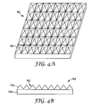
- FIG. 4A shows schematically an isometric view of another exemplary embodiment of an optical film according to the present disclosure
- FIG. 4B shows schematically a cross-sectional view of the optical film illustrated in FIG. 4A ;
- FIG. 5A shows schematically an isometric view of a further exemplary embodiment of an optical film according to the present disclosure
- FIG. 5B shows schematically a cross-sectional view of the optical film illustrated in FIG. 5A ;
- FIG. 6A shows schematically a top view of a rectangular-based prism of an exemplary optical film according to the present disclosure
- FIG. 6B shows schematically a cross-sectional view of the prism illustrated in FIG. 6A ;
- FIG. 6C shows schematically another cross-sectional view of the prism illustrated in FIG. 6A ;
- FIG. 7A shows schematically a cross-sectional view of a rectangular-based prism of an exemplary optical film according to the present disclosure, positioned over an LCD backlight;
- FIG. 7B shows schematically another cross-sectional view of the prism illustrated in FIG. 7A ;
- FIG. 8A shows schematically a top view of a rectangular-based prism of an exemplary optical film according to the present disclosure
- FIG. 8B shows schematically a top view of another rectangular-based prism of an exemplary optical film according to the present disclosure
- FIG. 9A shows schematically an isometric view of a further exemplary embodiment of an optical film according to the present disclosure.
- FIG. 9B shows a polar iso-candela plot for the optical film illustrated in FIG. 9A ;
- FIG. 9C shows a rectangular candela distribution plot for the optical film illustrated in FIG. 9A ;
- FIG. 10A shows schematically an isometric view of a further exemplary embodiment of an optical film according to the present disclosure
- FIG. 10B shows a polar iso-candela plot for the optical film illustrated in FIG. 10A ;
- FIG. 10C shows a rectangular candela distribution plot for the optical film illustrated in FIG. 10A ;
- FIG. 11A shows schematically an isometric view of a further exemplary embodiment of an optical film according to the present disclosure
- FIG. 11B shows a polar iso-candela plot for the optical film illustrated in FIG. 11A ;
- FIG. 11C shows a rectangular candela distribution plot for the optical film illustrated in FIG. 11A .
- the present disclosure is directed to an optical film for controlling the distribution of light from a light source and, in particular, for controlling light distribution along two different directions.
- the optical film according to the present disclosure may be useful in controlling the light distribution for an LCD backlight (e.g., LCD backlights shown in FIGS. 1A-1D ).
- FIGS. 1A-1D show several examples of backlights that may be used in LCDs.
- FIG. 1A shows a backlight 2 a .
- the backlight 2 a includes two light sources 4 a , such as two cold cathode fluorescent tubes (“CCFT”), that provide light from opposite sides or edges of the backlight, lamp reflectors 4 a ′ disposed about the light sources 4 a , a lightguide 3 a , which is illustrated as a substantially planar lightguide, a back reflector 3 a ′ and optical films 3 a ′′, which may be any suitable optical films.
- FIG. 1A shows a backlight 2 a .
- the backlight 2 a includes two light sources 4 a , such as two cold cathode fluorescent tubes (“CCFT”), that provide light from opposite sides or edges of the backlight, lamp reflectors 4 a ′ disposed about the light sources 4 a , a lightguide 3 a , which is illustrated as a substantially planar lightguide,
- FIG. 1B shows a backlight 2 b including a single light source 4 b , such as a CCFT, a lamp reflector 4 b ′ disposed about the light source 4 b , a lightguide 3 b , which is illustrated as a wedge-shaped lightguide, a back reflector 3 b ′ and optical films 3 b ′′, which may be any suitable optical films.
- FIG. 1C shows a backlight 2 c , which includes an extended light source 4 c .
- Exemplary suitable extended light sources include surface emission-type light sources.
- FIG. 1D shows schematically a partial view of a backlight 2 d , which includes three or more elongated linear light sources (e.g. CCFTs) 4 d , a back reflector 5 a , a diffuser plate 4 d ′ and optical films 4 d ′′, which may be any suitable optical films.
- Such backlights may be used in various display devices, such as LCD devices (e.g., televisions, monitors, etc).
- a display device may include a case having a window, a backlight situated in the case, an optical film according to the present disclosure, other suitable optical films, and a light valve arrangement, such as an LCD panel, situated between the optical film and the optical window.
- the optical film according to the present disclosure also may be used in conjunction with any other light source known to those of ordinary skill in the art and may include any other suitable elements.
- FIG. 2A shows a cross-sectional view of a backlight 2 e and an optical film 6 a according to the present disclosure.
- the backlight 2 e may include a light source 4 e , a lightguide 3 c , and a back reflector 5 b .
- the optical film 6 a may be positioned above the backlight 2 e .
- the optical film 6 a according to the present disclosure has a body that includes a structured surface 10 a and a substrate portion 12 a .
- the body of the optical film 6 a may be characterized by an axis, which in some exemplary embodiments is substantially perpendicular to the substrate portion 12 a and in other exemplary embodiments the axis makes a different angle with respect to the substrate portion 12 a.
- the body axis is substantially collinear with a viewing direction of a display device in which the optical films of the present disclosure can be used.
- the structured surface 10 a includes a plurality of prismatic structures 8 a , such as pyramidal prisms, which in some exemplary embodiments are rectangular-based prisms.
- the prismatic structures 8 a are arranged on the structured surface 10 a , in close proximity to one another, and, in some exemplary embodiments, in substantial contact or immediately adjacent with one another.
- the prismatic structures 8 a may be spaced from each other at any suitable distance (e.g., about ten (10) microns or more) provided that the gain of the optical film 6 a is at least about 1.1.
- gain is defined as the ratio of the axial output luminance of an optical system with an optical film constructed according to the present disclosure to the axial output luminance of the same optical system without such optical film.
- the size, shape and angles of the prismatic structures are selected to provide an optical gain of at least about 1.1.
- the spacing, size, shape and angles of the prismatic structures may be selected based on the desired output distribution of light.
- the prismatic structures should not be so small as to cause diffraction and should not be so large as to be seen with an unaided eye. The latter typically occurs for structures of about 100 micron in size.
- the spacing, size, shape and angles of the prismatic structures can be chosen so that the optical films of the present disclosure aid in hiding from the viewer light sources used in a direct-lit backlight.
- the structured surface 10 a is disposed on the substrate portion 12 a .
- the optical film 6 a may be used to change the direction and, in some cases, other characteristics of light rays emitted from the backlight 2 e .
- some embodiments of the present disclosure allow for the control of the angular spread of light using the prismatic structures 8 a of the optical film 6 a.
- the substrate portion 12 a has an additional optical characteristic that is different from the optical characteristics of the structured surface 10 a , such that the substrate portion manipulates light in a way that is different from the way light is manipulated by the structured surface 10 a .
- Such manipulation may include polarization, diffusion or additional redirection of light entering the optical films of the present disclosure. This may be accomplished, for example, by including in the substrate portion an optical film having such an additional optical characteristic or constructing the substrate portion itself to impart such an additional optical characteristic.
- Exemplary suitable films having such additional optical characteristics include, but are not limited to, a polarizer film, a diffuser film, a brightness enhancing film such as BEF, a turning film and any combination thereof.
- Turning film may be, for example, a reversed prism film (e.g., inverted BEF) or another structure that redirects light in a manner generally similar to that of a reversed prism film.
- the substrate portion 12 a may include a multilayer reflective polarizer, such as VikuitiTM Dual Brightness Enhancement Film (“DBEF”), or a diffuse reflective polarizer having a continuous phase and a disperse phase, such as VikuitiTM Diffuse Reflective Polarizer Film (“DRPF”), both available from 3M Company.
- DBEF VikuitiTM Dual Brightness Enhancement Film
- DRPF VikuitiTM Diffuse Reflective Polarizer Film
- the substrate portion may include a polycarbonate layer (“PC”), a poly methyl methacrylate layer (“PMMA”), a polyethylene terephthalate (“PET”) or any other suitable film or material known to those of ordinary skill in the art.
- PC polycarbonate layer
- PMMA poly methyl methacrylate layer
- PET polyethylene terephthalate
- FIGS. 3A and 3B show an exemplary embodiment of an optical film 6 c according to the present disclosure.
- a structured surface 10 c and a substrate portion 12 c may be parts of a single film, as shown in FIGS. 3A and 3B .
- the structured surface 10 c and the substrate portion 12 c may be formed as a single part, and in some cases from the same material, to produce the optical film 6 c , or they may be formed separately and then joined together to produce a single part, for example, using a suitable adhesive.
- the optical film 6 c may be manufactured by any method known to those of ordinary skill in the art including, but not limited to, embossing, casting, compression molding, and batch processes.
- a micro-structured form tool may be utilized to form the optical film (e.g. optical film 6 c ).
- the micro-structured form tool may be made, for example, by cutting groves in two directions on a suitable substrate.
- the resultant micro-structured form tool will include a plurality of prismatic structures resembling the desired optical film. The depth of the cut and spacing between each parallel cut may be adjusted depending on whether prismatic structures with sharp points, flats, or sharp lines along the peaks are desired and depending on other relevant parameters.
- An intermediary form tool with a reverse or opposite structure to the micro-structured form tool may be manufactured from the micro-structured form tool using, for example, an electro-plating method or polymer replication.
- the intermediary form tool may be comprised of polymers including, for example, polyurethane, polypropylene, acrylic, polycarbonate, polystyrene, a UV cured resin, etc.
- the intermediate tool may also be coated with a release layer in order to facilitate release of the final optical film.
- the intermediary form tool may be used to manufacture the optical film (e.g. optical film 6 c ) via direct replication or a batch process.
- the intermediary form tool may be used to batch process the optical film 6 c by such methods as injection molding, UV curing, or thermoplastic molding, such as compression molding.
- the optical film according to the present disclosure may be formed of or include any suitable material known to those of ordinary skill in the art including, for example, inorganic materials such as silica-based polymers, and organic materials, such as polymeric materials, including monomers, copolymers, grafted polymers, and mixtures or blends thereof.
- FIGS. 4A and 4B show another exemplary embodiment of an optical film 6 d according to the present disclosure.
- the optical film 6 d may be formed from two separate portions: a portion having a structured surface 10 d and a substrate portion 12 d .
- Such exemplary embodiments may be produced, for example, by coating the substrate portion with a curable material, imparting the structured surface into the curable material, and curing the optical film.
- a portion having a structured surface 10 e and a substrate portion 12 e of an optical film 6 e may be two separate films bonded together with a suitable adhesive 28 , for example, as illustrated in FIGS. 5A and 5B .
- the adhesive 28 may include, but is not limited to, a pressure sensitive adhesive (PSA) or an ultraviolet (UV) light curable adhesive.
- PSA pressure sensitive adhesive
- UV ultraviolet
- FIGS. 6A-6C An exemplary embodiment of prismatic structures 8 f according to the present disclosure is shown in FIGS. 6A-6C .
- FIG. 6A shows a top view of a prismatic structure 8 f .
- the base of the prismatic structure 8 f may be a four-sided shape with two first sides A 1 , disposed generally opposite to each other along a direction shown as 6 C, and two second sides B 1 , disposed generally opposite to each other along a direction shown as 6 B.
- the length of A 1 is less than the length of B 1
- the two first sides A 1 are substantially parallel to each other
- the two second sides B 1 are substantially parallel to each other.
- the first sides A 1 are substantially perpendicular to the second sides B 1 .
- the base of the prismatic structure 8 f may be substantially rectangular.
- FIG. 6B shows a cross-sectional view of an exemplary embodiment of a prismatic structure 8 f in the 6 B- 6 B plane as shown in FIG. 6A .
- the prismatic structure 8 f includes two surfaces 16 a .
- the prismatic structure 8 f also includes an angle ⁇ 1 (alpha) measured between one of the surfaces 16 a and a plane parallel to a substrate portion 12 f .
- FIG. 6C shows a cross-sectional view of an exemplary embodiment of the prismatic structure 8 f in the 6 C- 6 C plane as shown in FIG. 6A .
- the prismatic structure 8 f comprises two surfaces 14 a .
- the prismatic structure 8 f also includes an angle ⁇ 1 (beta) measured between one of the surfaces 14 a and a plane parallel to the substrate portion 12 f .
- the angle ⁇ 1 is preferably at least as great as the angle ⁇ 1 , and typically it is larger.
- FIGS. 6B and 6C show a light ray 18 traveling within the prismatic structure 8 f .
- the surface 16 a and the surface 14 a may reflect or refract the light ray 18 depending on an incident angle ⁇ 1 (delta) or ⁇ 2 of the light ray 18 with respect to a normal to the surface 16 a or the surface 14 a .
- ⁇ 1 and ⁇ 1 allows one to control the angular spread of light transmitted through the prismatic structures 8 f of an optical film 6 (e.g., optical film 6 a - 6 e ).
- the angles between the opposing pairs of surfaces and a plane parallel to a substrate portion are not equal to each other, which may be advantageous where a viewing axis that is tilted with respect to a normal to the substrate portion is desired.
- FIG. 7A shows a cross-sectional view of an exemplary embodiment of a prismatic structure 8 g similar to the prismatic structure 8 f shown in FIG. 6B .
- FIG. 7B shows a cross-sectional view of the exemplary embodiment of the prismatic structure 8 g similar to the prismatic structure 8 f shown in FIG. 6C .
- a light ray 20 b , a light ray 22 b , and a light ray 24 b which have the same directions as light rays 20 a , 22 a , and 24 a respectively, shown in FIG. 7A , originate from the backlight 2 g and propagate in the prismatic structure 8 g.
- FIGS. 7A and 7B show how a light ray may behave differently depending on whether it first impacts one of the surfaces 16 b or one of the surfaces 14 b , and how the angular spread of light may be controlled in two separate directions by selecting an angle ⁇ 2 of a surface 16 b and an angle ⁇ 2 of a surface 14 b .
- the light rays 20 - 24 are not drawn to precisely illustrate the angles of reflection and refraction of the light rays 20 - 24 .
- the light rays 20 - 24 are only shown to illustrate schematically the general direction of travel of the light rays through the prismatic structure 8 g.
- the light ray 20 a originating from the backlight display 2 g travels in the prismatic structure 8 g in a direction perpendicular to the surface 16 b .
- the light ray 20 a encounters the surface 16 b in a direction perpendicular (or normal) to the surface 16 b and an incident angle of the light ray 20 a relative to the normal of the surface 16 b is equal to zero (0) degrees.
- a medium above the optical film 6 (e.g., optical film 6 a - 6 e ) and the surfaces 16 b and 14 b may be, for example, comprised substantially of air.
- the medium above the optical film 6 and the surfaces 16 b and 14 b may be comprised of any medium, material, or film known to those of ordinary skill in the art.
- air has a refractive index less than most known materials. Based on the principles of Snell's Law, when light encounters, or is incident upon, a medium having a lesser refraction index, the light ray is bent away from the normal at an exit angle ⁇ relative to the normal that is greater than an incident angle ⁇ .
- n i the refractive index of the material on the side of incident light
- n t the refractive index of the material on the side of transmitted light
- ⁇ the exit angle
- FIG. 7B shows the light ray 20 b traveling in substantially the same direction as the light ray 20 a .
- the light ray 20 b encounters the surface 14 b at the incident angle ⁇ 3 relative to a normal to the surface 14 b .
- the angle ⁇ 2 of the surface 14 b is preferably less than the angle ⁇ 2 of the surface 16 b .
- the incident angle ⁇ 3 of the light ray 20 b is therefore not equal to the incident angle ⁇ of the light ray 20 a .
- the incident angle ⁇ 3 of the light ray 20 b is not equal to zero (0) as shown in FIG. 7B , and the light ray 20 b does not encounter the material-air boundary perpendicular to the surface 14 b .
- the light ray 20 b is refracted at an exit angle ⁇ 3 different from the incident angle ⁇ 3 at which it impacted the surface 14 b based on the formula of Snell's Law.
- the light ray 22 a travels into the prismatic structure 8 g and encounters the surface 16 b at the incident angle ⁇ 4 relative to the normal to the surface 16 b .
- the incident angle ⁇ 4 for the light ray 22 a is greater than the critical angle ⁇ c at the surface 16 b .
- the light ray 22 a does not exit the prismatic structure 8 g and is reflected back into the prismatic structure 8 g . This is referred to as “total internal reflection.”
- the light ray will behave according to the formula for refraction set forth above when traveling from a material having a higher refractive index to a material having a lower refractive index.
- the exit angle ⁇ will approach 90 degrees as the incident angle increases. However, at the critical angle ⁇ c , and for all angles greater than the critical angle ⁇ c , there will be total internal reflection (e.g., the light ray will be reflected back into the prismatic structure 8 g rather than being refracted and transmitted through the surface).
- the critical angle ⁇ c may be determined according to the Snell's Law (described above) by setting the exit angle (e.g., refraction angle) to ninety (90) degrees and solving for the incident angle ⁇ .
- the light ray 22 b traveling in substantially the same direction as the light ray 22 a , encounters the surface 14 b . Because the angle ⁇ 2 of the surface 14 b is less than the angle ⁇ 2 of the surface 16 b , the light ray 22 b encounters the surface 14 b at a different incident angle ⁇ 5 than the incident angle ⁇ 4 at which the light ray 22 a encountered the surface 16 b .
- the incident angle of light ray 22 b is less than the critical angle ⁇ c and, therefore, the light ray 22 b is refracted at the surface 14 b and transmitted through the surface 14 b.
- the light ray 24 a and the light ray 24 b travel in the prismatic structure 8 g in a direction perpendicular to the substrate portion 12 g .
- the light rays 24 a and 24 b encounter the surface 16 b and the surface 14 b , respectively, at incident angles ⁇ less than the critical angle ⁇ c .
- the incident angle ⁇ 6 of the light ray 24 a relative to the normal of the surface 16 b is greater than the incident angle ⁇ 7 of the light ray 24 b relative to the normal of the surface 14 b .
- the exit angle ⁇ 6 of the light ray 24 a relative to the normal of the surface 16 b will be different than the exit angle ⁇ 7 of the light ray relative to the normal to the surface 14 b .
- the exit angle ⁇ 6 of the light ray 24 a relative to the normal of the surface 16 b will be greater than the exit angle ⁇ 7 of the light ray 24 b relative to the normal of the surface 14 b.
- the surface 14 b with the lesser angle ⁇ 2 may generally “focus” more light toward a direction perpendicular to the backlight 2 g than the surface 16 b with the greater angle ⁇ 2 .
- the optical film 6 e.g., optical film 6 a - 6 e
- prismatic structures 8 e.g., prismatic structures 8 a - 8 g
- the optical film 6 may allow a greater angular spread of light along one direction and a lesser angular spread of light along another direction.
- the optical film 6 of the present disclosure may be employed in an LCD television to provide a wider angular spread of light in a first direction, e.g., the horizontal direction, and a lesser but still substantial angular spread of light in a second direction, e.g., the vertical direction.
- a first direction e.g., the horizontal direction
- a second direction e.g., the vertical direction.
- This may be advantageous to accommodate the normally wider field of view in the horizontal direction (e.g., viewers on either side of the television) than in the vertical direction (e.g., viewers standing or sitting).
- the viewing axis may be tilted downward, such as where a viewer may be sitting on the floor.
- FIGS. 8A and 8B illustrate further exemplary embodiments of the prismatic structures 8 according to the present disclosure.
- FIG. 8A shows a prismatic structure 8 h having two opposing first sides A 3 and two opposing second sides B 3 ; the length of A 3 is less than the length of B 3 .
- the prismatic structure 8 h also includes two surfaces 14 c and two surfaces 16 c .
- the prismatic structure 8 h further includes a substantially flat surface 26 a which is, preferably, 5% or less of a groove pitch to minimize gain loss.
- the flat surface 26 a may be useful, for example, when bonding a substrate portion 12 (e.g., substrate portion 12 a - 12 g ) or a further film on top of the prismatic structures 8 h of the structured surface 10 (e.g., structured surface 10 a - 10 e ). Furthermore, the flat surface may aid in transmitting more light in the direction perpendicular to the display (i.e., the direction along which a viewer is likely to view the screen).
- the surface 26 a may be raised or it may be depressed. In some exemplary embodiments, the surface 26 a may be rounded.
- FIG. 8B shows a prismatic structure 8 i having two opposing first sides A 4 and two opposing second sides B 4 .
- the two surfaces 14 d are of a substantially triangular shape and the two surfaces 16 d are of a substantially trapezoidal shape. It is contemplated that the prismatic structure 8 i may be of any other construction with two opposing first sides A 4 and two opposing second sides B 4 .
- FIGS. 9A, 10A , and 11 A show schematic partial perspective views of three additional exemplary embodiments of the optical film 6 j , 6 k , and 6 l , respectively, according to the present disclosure.
- the exemplary optical films 6 j / 6 k / 6 l include a portion having a structured surface 10 j / 10 k / 10 l with a refractive index of approximately 1.58, and a substrate portion 12 j / 12 k / 12 l having a refractive index of approximately 1.66.
- the structured surfaces 10 j / 10 k / 10 l include a plurality of prismatic structures 8 j / 8 k / 8 l .
- a base of the prismatic structures 8 j / 8 k / 8 l may be a four-sided shape with two first sides A 9 /A 10 /A 11 , disposed generally opposite to each other along a direction Y, and two second sides B 9 /B 10 /B 11 , disposed generally opposite to each other along a direction X.
- Each prismatic structure 8 j / 8 k / 8 l may also include two surfaces 14 j / 14 k / 14 l and two surfaces 16 j / 16 k / 16 l . As shown in FIGS.
- each of the surfaces 14 j / 14 k / 14 l meets one of the first side A 9 /A 10 /A 11 and each of the surfaces 16 j / 16 k / 16 l meets one of the second side B 9 /B 10 /B 11 .
- the surfaces 16 j / 16 k / 16 l and 14 j / 14 k / 14 l in the exemplary embodiments may be situated at a surface angle of about forty-five (45) degrees.
- the exemplary optical films 6 j / 6 k / 6 l and prismatic structures 8 j / 8 k / 8 l are further described in Table 1.
- the variable between the optical films 6 j , 6 k , and 6 l is the length of the second side B 9 /B 10 /B 11 of the base of each prismatic structure 8 j / 8 k / 8 l .
- the prism ratio in Table 1 is ratio of the length (e.g., B 9 /B 10 /B 11 ) of the base to the width (e.g., A 9 /A 10 /A 11 ) of the base.
- each optical film 6 j / 6 k / 6 l shown in Table 1 is the ratio of the peak axial luminance with the optical film 6 j / 6 k / 6 l divided to the peak axial luminance of light without the optical film 6 j / 6 k / 6 l .
- differences in the prism ratio do not significantly affect the axial gain of the exemplary embodiments of the optical film 6 j / 6 k / 6 l , while they can produce differences in angular distribution of light exiting the optical films of the present disclosure along two different directions.
- FIGS. 9B, 10B , and 11 B show polar iso-candela distribution plots for prismatic structures 8 j , 8 k , and 8 l , respectively.
- the candela distribution plots show a three hundred and sixty (360) degree pattern of detected incident light rays having passed through an optical film including prismatic structures, such as prismatic structures 8 j / 8 k / 8 l of the optical film 6 j / 6 k / 6 l .
- An exemplary prismatic structure 8 j / 8 k / 8 l is shown on each candela distribution plot for directional reference. As shown in FIGS.
- the light distribution differs for each of the optical films 6 j / 6 k / 6 l .
- the plot for the optical film 6 j shown in FIG. 9B which has the smallest prism ratio, shows a more symmetric distribution (i.e., the distribution of light along the X direction is more similar to distribution along the Y direction than those of FIGS. 10B and 11B ).
- the plot for the optical film 6 l shown in FIG. 11B which has the largest prism ratio of the three embodiments illustrated, shows the least symmetric distribution of the three (i.e., the distribution of light along the X direction is less than the distribution of light along the Y direction).
- the polar iso-candela distribution plots shown in FIGS. 9B, 10B , and 11 B demonstrate the ability of the exemplary embodiments to control the distribution of light along two different directions. As discussed above, this may be useful, for example, in devices such as LCD TVs or monitors to provide an extended viewing angle in one direction in a continuous manner.
- FIGS. 9C, 10C , and 11 C show rectangular candela distribution plots each corresponding to the polar plots shown in FIGS. 9B, 10B , and 11 B for the prismatic structures 8 j / 8 k / 8 l respectively.
- the rectangular candela distribution plots show the light intensity through the optical film 6 j / 6 k / 6 l at different angles. Each curve on the rectangular distribution plots corresponds to a different cross-section of the respective polar plot.
- the curves designated as 0 degrees represent the cross-section of the polar plots along the line passing through the center that connects 0 and 180 degrees
- the curves designated as 90 degrees represent the cross-section of the polar plots along the line passing through the center that connects 90 and 180 degrees
- the curves designated as 135 degrees represent the cross-section of the polar plots along the line passing through the center that connects 135 and 315 degrees.
- the plots for the optical film 6 l shown in FIG. 11C which has the largest prism ratio of the three embodiments illustrated, show the least symmetric distribution of the three (i.e., the distribution of light along the 0 degree direction is less than the distribution of light along the 90 degree direction).
Abstract
Described is an optical film having a structured surface including a plurality of prismatic structures. Each prismatic structure has a base including at least two longer sides disposed opposite to each other along a first general direction and at least two shorter sides disposed opposite to each other along a second general direction. The body transmits light incident thereon along the first general direction when an angle of incidence is within a first predetermined angle range with respect to the axis and reflects light when the angle of incidence is outside the first predetermined angle range. The body transmits light incident thereon along the second general direction when an angle of incidence is within a second predetermined angle range with respect to the axis and reflects light when the angle of incidence is outside the second predetermined angle range. The optical film further includes a substrate portion having an additional optical characteristic different from an optical characteristic of the structured surface. Display devices including such optical films are also disclosed.
Description
- The invention relates generally to light-transmissive optical films and in particular, to optical films with rectangular-based prisms.
- Display devices, such as liquid crystal display (“LCD”) devices, are used in a variety of applications including, for example, televisions, hand-held devices, digital still cameras, video cameras, and computer monitors. An LCD offers several advantages over a traditional cathode ray tube (“CRT”) display such as decreased weight, unit size and power consumption, as well as increased brightness. However, an LCD panel is not self-illuminating and, therefore, requires a backlighting assembly or a “backlight.” A backlight typically couples light from a substantially linear source (e.g., a cold cathode fluorescent tube (“CCFT”)) or light emitting diode (“LED”) to a substantially planar output. The planar output is then coupled to the LCD panel.
- The performance of an LCD is often judged by its brightness. Brightness of an LCD may be enhanced by using more or brighter light sources. In large area displays it is often necessary to use a direct-lit type LCD backlight to maintain brightness, because the space available for light sources grows linearly with the perimeter while the illuminated area grows as the square of the perimeter. Therefore, LCD televisions typically use a direct-lit backlight instead of a light-guide edge-lit type LCD backlight. Additional light sources and/or a brighter light source may consume more energy, which is counter to the ability to decrease the power allocation to the display device. For portable devices this may correlate to decreased battery life. Also, adding a light source to the display device may increase the product cost and sometimes can lead to reduced reliability of the display device.
- Brightness of an LCD may also be enhanced by efficiently utilizing the light that is available within the LCD device (e.g., to direct more of the available light within the display device along a preferred viewing axis). For example, Vikuiti™ Brightness Enhancement Film (“BEF”), available from 3M Corporation, has prismatic surface structures, which redirect some of the light exiting the backlight outside the viewing range to be substantially along the viewing axis. At least some of the remaining light is recycled via multiple reflections of some of the light between BEF and reflective components of the backlight, such as its back reflector. This results in optical gain substantially along the viewing axis, and also results in improved spatial uniformity of the illumination of the LCD. Thus, BEF is advantageous, for example, because it enhances brightness and improves spatial uniformity. For a battery powered portable device, this may translate to longer running times or smaller battery size, and a display that provides a better viewing experience.
- The present disclosure is directed to an optical film including a body having an axis and a structured surface including a plurality of prismatic structures, each prismatic structure having a base comprising at least two longer sides disposed opposite to each other along a first general direction and at least two shorter sides disposed opposite to each other along a second general direction. The body transmits a substantial portion of light incident thereon along the first general direction when an angle of incidence is within a first predetermined angle range with respect to the axis and reflects a substantial portion of light when the angle of incidence is outside the first predetermined angle range. The body further transmits a substantial portion of light incident thereon along the second general direction when an angle of incidence is within a second predetermined angle range with respect to the axis and reflects a substantial portion of light when the angle of incidence is outside the second predetermined angle range. The optical film further comprises a substrate portion having an additional optical characteristic different from an optical characteristic of the structured surface.
- The present disclosure is also directed to a display device including a case having a window; a backlight situated in the case, an optical film situated between the backlight and the window; and a light valve arrangement situated between the optical film and the optical window. The optical film includes a body having an axis and a structured surface including a plurality of prismatic structures, each prismatic structure having a base including two longer sides disposed opposite to each other along a first general direction and two shorter sides disposed opposite to each other along a second general direction. The body transmits a substantial portion of light incident thereon along the first general direction when an angle of incidence is within a first predetermined angle range with respect to the axis and reflects a substantial portion of light when the angle of incidence is outside the first predetermined angle range. The body further transmits a substantial portion of light incident thereon along the second general direction when an angle of incidence is within a second predetermined angle range with respect to the axis and reflects a substantial portion of light when the angle of incidence is outside the second predetermined angle range. The optical film further comprises a substrate portion having an additional optical characteristic different from an optical characteristic of the structured surface.
- So that those of ordinary skill in the art to which the subject invention pertains will more readily understand how to make and use the subject invention, exemplary embodiments thereof are described in detail below with reference to the drawings, wherein:
-
FIG. 1A shows schematically a flat light-guide edge-lit LCD backlight; -
FIG. 1B shows schematically a wedge light-guide edge-lit LCD backlight; -
FIG. 1C shows schematically an LCD backlight utilizing an extended light source; -
FIG. 1D shows schematically a direct-lit type LCD backlight; -
FIG. 2A shows schematically an exemplary embodiment of an optical film according to the present disclosure positioned over an LCD backlight; -
FIG. 3A shows schematically an isometric view of an exemplary embodiment of an optical film according to the present disclosure; -
FIG. 3B shows schematically a cross-sectional view of the optical film illustrated inFIG. 3A ; -
FIG. 4A shows schematically an isometric view of another exemplary embodiment of an optical film according to the present disclosure; -
FIG. 4B shows schematically a cross-sectional view of the optical film illustrated inFIG. 4A ; -
FIG. 5A shows schematically an isometric view of a further exemplary embodiment of an optical film according to the present disclosure; -
FIG. 5B shows schematically a cross-sectional view of the optical film illustrated inFIG. 5A ; -
FIG. 6A shows schematically a top view of a rectangular-based prism of an exemplary optical film according to the present disclosure; -
FIG. 6B shows schematically a cross-sectional view of the prism illustrated inFIG. 6A ; -
FIG. 6C shows schematically another cross-sectional view of the prism illustrated inFIG. 6A ; -
FIG. 7A shows schematically a cross-sectional view of a rectangular-based prism of an exemplary optical film according to the present disclosure, positioned over an LCD backlight; -
FIG. 7B shows schematically another cross-sectional view of the prism illustrated inFIG. 7A ; -
FIG. 8A shows schematically a top view of a rectangular-based prism of an exemplary optical film according to the present disclosure; -
FIG. 8B shows schematically a top view of another rectangular-based prism of an exemplary optical film according to the present disclosure; -
FIG. 9A shows schematically an isometric view of a further exemplary embodiment of an optical film according to the present disclosure; -
FIG. 9B shows a polar iso-candela plot for the optical film illustrated inFIG. 9A ; -
FIG. 9C shows a rectangular candela distribution plot for the optical film illustrated inFIG. 9A ; -
FIG. 10A shows schematically an isometric view of a further exemplary embodiment of an optical film according to the present disclosure; -
FIG. 10B shows a polar iso-candela plot for the optical film illustrated inFIG. 10A ; -
FIG. 10C shows a rectangular candela distribution plot for the optical film illustrated inFIG. 10A ; -
FIG. 11A shows schematically an isometric view of a further exemplary embodiment of an optical film according to the present disclosure; -
FIG. 11B shows a polar iso-candela plot for the optical film illustrated inFIG. 11A ; and -
FIG. 11C shows a rectangular candela distribution plot for the optical film illustrated inFIG. 11A . - The present disclosure is directed to an optical film for controlling the distribution of light from a light source and, in particular, for controlling light distribution along two different directions. The optical film according to the present disclosure may be useful in controlling the light distribution for an LCD backlight (e.g., LCD backlights shown in
FIGS. 1A-1D ). -
FIGS. 1A-1D show several examples of backlights that may be used in LCDs.FIG. 1A shows abacklight 2 a. Thebacklight 2 a includes twolight sources 4 a, such as two cold cathode fluorescent tubes (“CCFT”), that provide light from opposite sides or edges of the backlight,lamp reflectors 4 a′ disposed about thelight sources 4 a, alightguide 3 a, which is illustrated as a substantially planar lightguide, aback reflector 3 a′ andoptical films 3 a″, which may be any suitable optical films.FIG. 1B shows abacklight 2 b including a singlelight source 4 b, such as a CCFT, alamp reflector 4 b′ disposed about thelight source 4 b, alightguide 3 b, which is illustrated as a wedge-shaped lightguide, aback reflector 3 b′ andoptical films 3 b″, which may be any suitable optical films.FIG. 1C shows abacklight 2 c, which includes an extendedlight source 4 c. Exemplary suitable extended light sources include surface emission-type light sources.FIG. 1D shows schematically a partial view of abacklight 2 d, which includes three or more elongated linear light sources (e.g. CCFTs) 4 d, aback reflector 5 a, adiffuser plate 4 d′ andoptical films 4 d″, which may be any suitable optical films. - Such backlights may be used in various display devices, such as LCD devices (e.g., televisions, monitors, etc). As one of ordinary skill in the art will understand, a display device may include a case having a window, a backlight situated in the case, an optical film according to the present disclosure, other suitable optical films, and a light valve arrangement, such as an LCD panel, situated between the optical film and the optical window. The optical film according to the present disclosure also may be used in conjunction with any other light source known to those of ordinary skill in the art and may include any other suitable elements.
-
FIG. 2A shows a cross-sectional view of abacklight 2 e and anoptical film 6 a according to the present disclosure. Thebacklight 2 e may include alight source 4 e, alightguide 3 c, and aback reflector 5 b. Theoptical film 6 a may be positioned above thebacklight 2 e. Theoptical film 6 a according to the present disclosure has a body that includes a structuredsurface 10 a and asubstrate portion 12 a. The body of theoptical film 6 a may be characterized by an axis, which in some exemplary embodiments is substantially perpendicular to thesubstrate portion 12 a and in other exemplary embodiments the axis makes a different angle with respect to thesubstrate portion 12 a. - In typical embodiments of the present disclosure, the body axis is substantially collinear with a viewing direction of a display device in which the optical films of the present disclosure can be used. The structured
surface 10 a includes a plurality ofprismatic structures 8 a, such as pyramidal prisms, which in some exemplary embodiments are rectangular-based prisms. Theprismatic structures 8 a are arranged on the structuredsurface 10 a, in close proximity to one another, and, in some exemplary embodiments, in substantial contact or immediately adjacent with one another. However, in other exemplary embodiments, theprismatic structures 8 a may be spaced from each other at any suitable distance (e.g., about ten (10) microns or more) provided that the gain of theoptical film 6 a is at least about 1.1. - For the purposes of the present disclosure, “gain” is defined as the ratio of the axial output luminance of an optical system with an optical film constructed according to the present disclosure to the axial output luminance of the same optical system without such optical film. In typical embodiments of the present disclosure, the size, shape and angles of the prismatic structures are selected to provide an optical gain of at least about 1.1. In addition, the spacing, size, shape and angles of the prismatic structures may be selected based on the desired output distribution of light. However, the prismatic structures should not be so small as to cause diffraction and should not be so large as to be seen with an unaided eye. The latter typically occurs for structures of about 100 micron in size. In some exemplary embodiments that are particularly suitable for use in direct-lit backlights, the spacing, size, shape and angles of the prismatic structures can be chosen so that the optical films of the present disclosure aid in hiding from the viewer light sources used in a direct-lit backlight. In the exemplary embodiment shown in
FIG. 2A , the structuredsurface 10 a is disposed on thesubstrate portion 12 a. As one of ordinary skill in the art would understand, theoptical film 6 a may be used to change the direction and, in some cases, other characteristics of light rays emitted from thebacklight 2 e. For example, some embodiments of the present disclosure allow for the control of the angular spread of light using theprismatic structures 8 a of theoptical film 6 a. - The
substrate portion 12 a has an additional optical characteristic that is different from the optical characteristics of the structuredsurface 10 a, such that the substrate portion manipulates light in a way that is different from the way light is manipulated by the structuredsurface 10 a. Such manipulation may include polarization, diffusion or additional redirection of light entering the optical films of the present disclosure. This may be accomplished, for example, by including in the substrate portion an optical film having such an additional optical characteristic or constructing the substrate portion itself to impart such an additional optical characteristic. Exemplary suitable films having such additional optical characteristics include, but are not limited to, a polarizer film, a diffuser film, a brightness enhancing film such as BEF, a turning film and any combination thereof. Turning film may be, for example, a reversed prism film (e.g., inverted BEF) or another structure that redirects light in a manner generally similar to that of a reversed prism film. In some exemplary embodiments, thesubstrate portion 12 a may include a multilayer reflective polarizer, such as Vikuiti™ Dual Brightness Enhancement Film (“DBEF”), or a diffuse reflective polarizer having a continuous phase and a disperse phase, such as Vikuiti™ Diffuse Reflective Polarizer Film (“DRPF”), both available from 3M Company. In other exemplary embodiments, the substrate portion may include a polycarbonate layer (“PC”), a poly methyl methacrylate layer (“PMMA”), a polyethylene terephthalate (“PET”) or any other suitable film or material known to those of ordinary skill in the art. -
FIGS. 3A and 3B show an exemplary embodiment of anoptical film 6 c according to the present disclosure. Astructured surface 10 c and asubstrate portion 12 c may be parts of a single film, as shown inFIGS. 3A and 3B . As one of ordinary skill in the art would understand, the structuredsurface 10 c and thesubstrate portion 12 c may be formed as a single part, and in some cases from the same material, to produce theoptical film 6 c, or they may be formed separately and then joined together to produce a single part, for example, using a suitable adhesive. Theoptical film 6 c may be manufactured by any method known to those of ordinary skill in the art including, but not limited to, embossing, casting, compression molding, and batch processes. - In an exemplary method of manufacturing an optical film according to the present disclosure, a micro-structured form tool, and optionally an intermediate form tool, may be utilized to form the optical film (e.g.
optical film 6 c). The micro-structured form tool may be made, for example, by cutting groves in two directions on a suitable substrate. As one of ordinary skill in the art will understand, the resultant micro-structured form tool will include a plurality of prismatic structures resembling the desired optical film. The depth of the cut and spacing between each parallel cut may be adjusted depending on whether prismatic structures with sharp points, flats, or sharp lines along the peaks are desired and depending on other relevant parameters. - An intermediary form tool with a reverse or opposite structure to the micro-structured form tool (e.g. inverted prismatic structures) may be manufactured from the micro-structured form tool using, for example, an electro-plating method or polymer replication. The intermediary form tool may be comprised of polymers including, for example, polyurethane, polypropylene, acrylic, polycarbonate, polystyrene, a UV cured resin, etc. The intermediate tool may also be coated with a release layer in order to facilitate release of the final optical film.
- As one of ordinary skill in the art will understand, the intermediary form tool may be used to manufacture the optical film (e.g.
optical film 6 c) via direct replication or a batch process. For example, the intermediary form tool may be used to batch process theoptical film 6 c by such methods as injection molding, UV curing, or thermoplastic molding, such as compression molding. The optical film according to the present disclosure may be formed of or include any suitable material known to those of ordinary skill in the art including, for example, inorganic materials such as silica-based polymers, and organic materials, such as polymeric materials, including monomers, copolymers, grafted polymers, and mixtures or blends thereof. -
FIGS. 4A and 4B show another exemplary embodiment of anoptical film 6 d according to the present disclosure. In particular, theoptical film 6 d may be formed from two separate portions: a portion having a structuredsurface 10 d and asubstrate portion 12 d. Such exemplary embodiments may be produced, for example, by coating the substrate portion with a curable material, imparting the structured surface into the curable material, and curing the optical film. Alternatively, a portion having a structuredsurface 10 e and asubstrate portion 12 e of anoptical film 6 e may be two separate films bonded together with asuitable adhesive 28, for example, as illustrated inFIGS. 5A and 5B . The adhesive 28 may include, but is not limited to, a pressure sensitive adhesive (PSA) or an ultraviolet (UV) light curable adhesive. In such exemplary embodiments, it is sometimes advantageous to make the portion having a structured surface from a material with a refractive index lower than the refractive index of the substrate portion. - An exemplary embodiment of
prismatic structures 8 f according to the present disclosure is shown inFIGS. 6A-6C .FIG. 6A shows a top view of aprismatic structure 8 f. The base of theprismatic structure 8 f may be a four-sided shape with two first sides A1, disposed generally opposite to each other along a direction shown as 6C, and two second sides B1, disposed generally opposite to each other along a direction shown as 6B. In typical embodiments of the present disclosure, the length of A1 is less than the length of B1, the two first sides A1 are substantially parallel to each other, and the two second sides B1 are substantially parallel to each other. In some exemplary embodiments, the first sides A1 are substantially perpendicular to the second sides B1. Thus, the base of theprismatic structure 8 f may be substantially rectangular. -
FIG. 6B shows a cross-sectional view of an exemplary embodiment of aprismatic structure 8 f in the 6B-6B plane as shown inFIG. 6A . Theprismatic structure 8 f includes twosurfaces 16 a. Theprismatic structure 8 f also includes an angle α1 (alpha) measured between one of thesurfaces 16 a and a plane parallel to asubstrate portion 12 f.FIG. 6C shows a cross-sectional view of an exemplary embodiment of theprismatic structure 8 f in the 6C-6C plane as shown inFIG. 6A . Theprismatic structure 8 f comprises twosurfaces 14 a. Theprismatic structure 8 f also includes an angle β1 (beta) measured between one of thesurfaces 14 a and a plane parallel to thesubstrate portion 12 f. The angle α1 is preferably at least as great as the angle β1, and typically it is larger. -
FIGS. 6B and 6C show alight ray 18 traveling within theprismatic structure 8 f. Thesurface 16 a and thesurface 14 a may reflect or refract thelight ray 18 depending on an incident angle δ1 (delta) or δ2 of thelight ray 18 with respect to a normal to thesurface 16 a or thesurface 14 a. As one of ordinary skill in the art will understand from the present disclosure, selecting different angles α1 and β1 allows one to control the angular spread of light transmitted through theprismatic structures 8 f of an optical film 6 (e.g., optical film 6 a-6 e). In some exemplary embodiments, the angles between the opposing pairs of surfaces and a plane parallel to a substrate portion are not equal to each other, which may be advantageous where a viewing axis that is tilted with respect to a normal to the substrate portion is desired. -
FIG. 7A shows a cross-sectional view of an exemplary embodiment of a prismatic structure 8 g similar to theprismatic structure 8 f shown inFIG. 6B . Alight ray 20 a, alight ray 22 a, and alight ray 24 a, emitted from abacklight 2 g, propagate in the prismatic structure 8 g.FIG. 7B shows a cross-sectional view of the exemplary embodiment of the prismatic structure 8 g similar to theprismatic structure 8 f shown inFIG. 6C . Alight ray 20 b, alight ray 22 b, and alight ray 24 b, which have the same directions aslight rays FIG. 7A , originate from thebacklight 2 g and propagate in the prismatic structure 8 g. - The following describes the travel of each of the light rays 20-24, originating from the
LCD backlight 2 g, through the prismatic structures 8 g of an optical film 6 of the present disclosure (e.g., optical film 6 a-6 e).FIGS. 7A and 7B show how a light ray may behave differently depending on whether it first impacts one of thesurfaces 16 b or one of thesurfaces 14 b, and how the angular spread of light may be controlled in two separate directions by selecting an angle δ2 of asurface 16 b and an angle δ2 of asurface 14 b. It should be noted that the light rays 20-24 are not drawn to precisely illustrate the angles of reflection and refraction of the light rays 20-24. The light rays 20-24 are only shown to illustrate schematically the general direction of travel of the light rays through the prismatic structure 8 g. - In
FIG. 7A , thelight ray 20 a originating from thebacklight display 2 g travels in the prismatic structure 8 g in a direction perpendicular to thesurface 16 b. Thus, thelight ray 20 a encounters thesurface 16 b in a direction perpendicular (or normal) to thesurface 16 b and an incident angle of thelight ray 20 a relative to the normal of thesurface 16 b is equal to zero (0) degrees. - A medium above the optical film 6 (e.g., optical film 6 a-6 e) and the
surfaces surfaces light ray 20 a) is not bent and continues to travel in a straight line as shown inFIG. 7A . Snell's Law can be expressed by the formula:
n i*sin δ=n t*sin θ, - where,
- ni=the refractive index of the material on the side of incident light,
- δ=the incident angle,
- nt=the refractive index of the material on the side of transmitted light, and
- θ=the exit angle.
- Those of ordinary skill in the art will understand that a certain amount of the incident light will also be reflected back into the prismatic structure 8 g.
-
FIG. 7B shows thelight ray 20 b traveling in substantially the same direction as thelight ray 20 a. Thelight ray 20 b encounters thesurface 14 b at the incident angle δ3 relative to a normal to thesurface 14 b. As discussed above, the angle β2 of thesurface 14 b is preferably less than the angle α2 of thesurface 16 b. Thus, the incident angle δ3 of thelight ray 20 b is therefore not equal to the incident angle δ of thelight ray 20 a. The incident angle δ3 of thelight ray 20 b is not equal to zero (0) as shown inFIG. 7B , and thelight ray 20 b does not encounter the material-air boundary perpendicular to thesurface 14 b. Thelight ray 20 b is refracted at an exit angle θ3 different from the incident angle δ3 at which it impacted thesurface 14 b based on the formula of Snell's Law. - As shown in
FIG. 7A , thelight ray 22 a travels into the prismatic structure 8 g and encounters thesurface 16 b at the incident angle δ4 relative to the normal to thesurface 16 b. The incident angle δ4 for thelight ray 22 a is greater than the critical angle δc at thesurface 16 b. Thelight ray 22 a does not exit the prismatic structure 8 g and is reflected back into the prismatic structure 8 g. This is referred to as “total internal reflection.” As described above, the light ray will behave according to the formula for refraction set forth above when traveling from a material having a higher refractive index to a material having a lower refractive index. According to the formula, the exit angle θ will approach 90 degrees as the incident angle increases. However, at the critical angle δc, and for all angles greater than the critical angle δc, there will be total internal reflection (e.g., the light ray will be reflected back into the prismatic structure 8 g rather than being refracted and transmitted through the surface). As one of ordinary skill in the art would understand, the critical angle δc may be determined according to the Snell's Law (described above) by setting the exit angle (e.g., refraction angle) to ninety (90) degrees and solving for the incident angle δ. - As shown in
FIG. 7B , thelight ray 22 b, traveling in substantially the same direction as thelight ray 22 a, encounters thesurface 14 b. Because the angle β2 of thesurface 14 b is less than the angle α2 of thesurface 16 b, thelight ray 22 b encounters thesurface 14 b at a different incident angle δ5 than the incident angle δ4 at which thelight ray 22 a encountered thesurface 16 b. The incident angle oflight ray 22 b is less than the critical angle δc and, therefore, thelight ray 22 b is refracted at thesurface 14 b and transmitted through thesurface 14 b. - The
light ray 24 a and thelight ray 24 b, shown inFIGS. 7A and 7B respectively, travel in the prismatic structure 8 g in a direction perpendicular to thesubstrate portion 12 g. The light rays 24 a and 24 b encounter thesurface 16 b and thesurface 14 b, respectively, at incident angles δ less than the critical angle δc. However, the incident angle δ6 of thelight ray 24 a relative to the normal of thesurface 16 b is greater than the incident angle δ7 of thelight ray 24 b relative to the normal of thesurface 14 b. Hence, according to Snell's Law, the exit angle θ6 of thelight ray 24 a relative to the normal of thesurface 16 b will be different than the exit angle θ7 of the light ray relative to the normal to thesurface 14 b. As one of ordinary skill in the art would understand, the exit angle θ6 of thelight ray 24 a relative to the normal of thesurface 16 b will be greater than the exit angle θ7 of thelight ray 24 b relative to the normal of thesurface 14 b. - As one of ordinary skill in the art would understand, the
surface 14 b with the lesser angle β2 may generally “focus” more light toward a direction perpendicular to thebacklight 2 g than thesurface 16 b with the greater angle α2. Thus, the optical film 6 (e.g., optical film 6 a-6 e) with prismatic structures 8 (e.g., prismatic structures 8 a-8 g) as described may allow a greater angular spread of light along one direction and a lesser angular spread of light along another direction. For example, the optical film 6 of the present disclosure may be employed in an LCD television to provide a wider angular spread of light in a first direction, e.g., the horizontal direction, and a lesser but still substantial angular spread of light in a second direction, e.g., the vertical direction. This may be advantageous to accommodate the normally wider field of view in the horizontal direction (e.g., viewers on either side of the television) than in the vertical direction (e.g., viewers standing or sitting). In some exemplary embodiments, the viewing axis may be tilted downward, such as where a viewer may be sitting on the floor. By reducing the angular spread of light in the vertical direction, a resultant optical gain may be experienced in a desired viewing angle range. -
FIGS. 8A and 8B illustrate further exemplary embodiments of the prismatic structures 8 according to the present disclosure.FIG. 8A shows aprismatic structure 8 h having two opposing first sides A3 and two opposing second sides B3; the length of A3 is less than the length of B3. Theprismatic structure 8 h also includes twosurfaces 14 c and twosurfaces 16 c. In this exemplary embodiment, theprismatic structure 8 h further includes a substantiallyflat surface 26 a which is, preferably, 5% or less of a groove pitch to minimize gain loss. Theflat surface 26 a may be useful, for example, when bonding a substrate portion 12 (e.g., substrate portion 12 a-12 g) or a further film on top of theprismatic structures 8 h of the structured surface 10 (e.g., structured surface 10 a-10 e). Furthermore, the flat surface may aid in transmitting more light in the direction perpendicular to the display (i.e., the direction along which a viewer is likely to view the screen). Thesurface 26 a may be raised or it may be depressed. In some exemplary embodiments, thesurface 26 a may be rounded. -
FIG. 8B shows aprismatic structure 8 i having two opposing first sides A4 and two opposing second sides B4. In this exemplary embodiment, the twosurfaces 14 d are of a substantially triangular shape and the two surfaces 16 d are of a substantially trapezoidal shape. It is contemplated that theprismatic structure 8 i may be of any other construction with two opposing first sides A4 and two opposing second sides B4. -
FIGS. 9A, 10A , and 11A show schematic partial perspective views of three additional exemplary embodiments of theoptical film 6 j, 6 k, and 6 l, respectively, according to the present disclosure. The exemplary optical films 6 j/6 k/6 l include a portion having a structuredsurface 10 j/10 k/10 l with a refractive index of approximately 1.58, and asubstrate portion 12 j/12 k/12 l having a refractive index of approximately 1.66. The structured surfaces 10 j/10 k/10 l include a plurality ofprismatic structures 8 j/8 k/8 l. A base of theprismatic structures 8 j/8 k/8 l may be a four-sided shape with two first sides A9/A10/A11, disposed generally opposite to each other along a direction Y, and two second sides B9/B10/B11, disposed generally opposite to each other along a direction X. Eachprismatic structure 8 j/8 k/8 l may also include twosurfaces 14 j/14 k/14 l and twosurfaces 16 j/16 k/16 l. As shown inFIGS. 9A, 10A , and 11A, each of thesurfaces 14 j/14 k/14 l meets one of the first side A9/A10/A11 and each of thesurfaces 16 j/16 k/16 l meets one of the second side B9/B10/B11. Thesurfaces 16 j/16 k/16 l and 14 j/14 k/14 l in the exemplary embodiments may be situated at a surface angle of about forty-five (45) degrees. The exemplary optical films 6 j/6 k/6 l andprismatic structures 8 j/8 k/8 l are further described in Table 1.TABLE 1 Optical Films 6j, 6k, 6l6j 6k 6l Number of Prisms long 20 20 20 Number of Prisms wide 20 20 20 Prism Length, B (mils) 2.2 2.8 6 Prism Width, A (mils) 2 2 2 Prism ratio (Length B/width A) 1.1 1.4 3 Optical film length (mils) 44 56 120 Optical film width (mils) 40 40 40 Optical film thickness (mils) 4 4 4 Light source length (mils) 22 28 60 Light source width (mils) 20 20 20 Light source position, length (mils) 22 28 60 Light source position, width (mils) 20 20 20 Peak light (Watts/steradian) 0.28857 0.28838 0.28703 Efficiency (% light flux) 0.43431 0.43065 0.43832 Gain 1.612665 1.620833 1.60381 - As shown in Table 1, the variable between the
optical films 6 j, 6 k, and 6 l is the length of the second side B9/B10/B11 of the base of eachprismatic structure 8 j/8 k/8 l. The prism ratio in Table 1 is ratio of the length (e.g., B9/B10/B11) of the base to the width (e.g., A9/A10/A11) of the base. The gain of each optical film 6 j/6 k/6 l shown in Table 1 is the ratio of the peak axial luminance with the optical film 6 j/6 k/6 l divided to the peak axial luminance of light without the optical film 6 j/6 k/6 l. As one of ordinary skill in the art will understand from Table 1, differences in the prism ratio do not significantly affect the axial gain of the exemplary embodiments of the optical film 6 j/6 k/6 l, while they can produce differences in angular distribution of light exiting the optical films of the present disclosure along two different directions. -
FIGS. 9B, 10B , and 11B show polar iso-candela distribution plots forprismatic structures prismatic structures 8 j/8 k/8 l of the optical film 6 j/6 k/6 l. An exemplaryprismatic structure 8 j/8 k/8 l is shown on each candela distribution plot for directional reference. As shown inFIGS. 9B, 10B , and 11B, the light distribution differs for each of the optical films 6 j/6 k/6 l. For example, the plot for the optical film 6 j shown inFIG. 9B , which has the smallest prism ratio, shows a more symmetric distribution (i.e., the distribution of light along the X direction is more similar to distribution along the Y direction than those ofFIGS. 10B and 11B ). The plot for the optical film 6 l shown inFIG. 11B , which has the largest prism ratio of the three embodiments illustrated, shows the least symmetric distribution of the three (i.e., the distribution of light along the X direction is less than the distribution of light along the Y direction). - As one of ordinary skill in the art will understand, the polar iso-candela distribution plots shown in
FIGS. 9B, 10B , and 11B demonstrate the ability of the exemplary embodiments to control the distribution of light along two different directions. As discussed above, this may be useful, for example, in devices such as LCD TVs or monitors to provide an extended viewing angle in one direction in a continuous manner. -
FIGS. 9C, 10C , and 11C show rectangular candela distribution plots each corresponding to the polar plots shown inFIGS. 9B, 10B , and 11B for theprismatic structures 8 j/8 k/8 l respectively. As one of ordinary skill in the art will understand, the rectangular candela distribution plots show the light intensity through the optical film 6 j/6 k/6 l at different angles. Each curve on the rectangular distribution plots corresponds to a different cross-section of the respective polar plot. For example, the curves designated as 0 degrees represent the cross-section of the polar plots along the line passing through the center that connects 0 and 180 degrees, the curves designated as 90 degrees represent the cross-section of the polar plots along the line passing through the center that connects 90 and 180 degrees, and the curves designated as 135 degrees represent the cross-section of the polar plots along the line passing through the center that connects 135 and 315 degrees. As in the previous set of graphs, the plots for the optical film 6 l shown inFIG. 11C , which has the largest prism ratio of the three embodiments illustrated, show the least symmetric distribution of the three (i.e., the distribution of light along the 0 degree direction is less than the distribution of light along the 90 degree direction). - It will be apparent to those skilled in the art that various modifications and variations can be made in the structure and the methodology of the present disclosure, without departing from the spirit or scope of the invention. Thus, it is intended that the present disclosure cover the modifications and variations of the exemplary embodiments described herein, provided that they come within the scope of the appended claims and their equivalents.
Claims (31)
1. An optical film, comprising:
a body having an axis and a structured surface including a plurality of prismatic structures, each prismatic structure having a base including at least two longer sides disposed opposite to each other along a first general direction and at least two shorter sides disposed opposite to each other along a second general direction,
wherein the body transmits a substantial portion of light incident thereon along the first general direction when an angle of incidence is within a first predetermined angle range with respect to the axis and reflects a substantial portion of light when the angle of incidence is outside the first predetermined angle range, and
wherein the body transmits a substantial portion of light incident thereon along the second general direction when an angle of incidence is within a second predetermined angle range with respect to the axis and reflects a substantial portion of light when the angle of incidence is outside the second predetermined angle range; and
the body comprises a substrate portion having an additional optical characteristic different from an optical characteristic of the structured surface.
2. The optical film according to claim 1 , wherein the base has a substantially rectangular shape.
3. The optical film according to claim 1 , wherein each prismatic structure is arranged in a substantial contact with at least one other prismatic structure.
4. The optical film according to claim 1 , wherein the bases of the plurality of prismatic structures are aligned with the two longer sides of each of the bases extending along the first general direction substantially parallel to one another.
5. The optical film according to claim 1 , wherein the substrate portion comprises at least one of: a polarizer film, a diffuser film, a brightness enhancing film, and a turning film.
6. The optical film according to claim 1 , wherein the structured surface is disposed on a body portion that is different from the substrate portion, said substrate portion and the body portion are attached to each other.
7. The optical film according to claim 6 , wherein the body portion and the substrate portion each have a refractive index, the refractive index of the body portion being lower than the refractive index of the substrate portion.
8. The optical film according to claim 1 , wherein the structured surface is disposed on the substrate portion.
9. The optical film according to claim 1 , wherein each of the prismatic structures includes at least four surfaces, each of the four surfaces being attached to the base.
10. The optical film according to claim 9 , wherein at least four surfaces meet.
11. The optical film according to claim 9 , wherein two of the at least four surfaces meet.
12. The optical film according to claim 1 , wherein each of the prismatic structures comprises five surfaces, four surfaces being attached to the base, a fifth surface being adjacent to the four surfaces and situated substantially parallel to the base.
13. The backlight display device according to claim 1 , wherein the first predetermined angle range is greater than the second predetermined angle range.
14. A display device comprising:
a case having a window;
a backlight situated in the case,
an optical film situated between the backlight and the window, and
a light valve arrangement situated between the optical film and the optical window;
wherein the optical film includes a body having an axis and a structured surface including a plurality of prismatic structures, each prismatic structure having a base including two longer sides disposed opposite to each other along a first general direction and two shorter sides disposed opposite to each other along a second general direction,
wherein the body transmits a substantial portion of light incident thereon along the first general direction when an angle of incidence is within a first predetermined angle range with respect to the axis and reflects a substantial portion of light when the angle of incidence is outside the first predetermined angle range,
wherein the body transmits a substantial portion of light incident thereon along the second general direction when an angle of incidence is within a second predetermined angle with respect to the axis and reflects a substantial portion of light when the angle of incidence is outside the second predetermined angle range, and
wherein the body further comprises a substrate portion having an additional optical characteristic different from an optical characteristic of the structured surface.
15. The backlight display device according to claim 14 , wherein the backlight panel is side lit.
16. The backlight display device according to claim 14 , wherein the backlight panel is direct lit.
17. The backlight display device according to claim 14 , wherein the light valve arrangement is a liquid crystal display panel.
18. The backlight display device according to claim 14 , wherein the base of the prismatic structure has a substantially rectangular shape.
19. The backlight display device according to claim 14 , wherein each prismatic structure is arranged in a substantial contact with each other.
20. The backlight display device according to claim 14 , wherein the rectangular bases of the plurality of prismatic structures are aligned with the two longer sides of each of the bases extending along the first general direction substantially parallel to one another.
21. The backlight display device according to claim 14 , wherein the substrate portion comprises at least one of a polarizer film, a diffuser film, a brightness enhancing film, and a turning film.
22. The optical film according to claim 14 , wherein the structured surface is disposed on a body portion that is different from the substrate portion, said substrate portion and the body portion are attached to each other.
23. The optical film according to claim 22 , wherein the body portion and the substrate portion each have a refractive index, the refractive index of the body portion being lower than the refractive index of the substrate portion.
24. The backlight display device according to claim 14 , wherein the structured surface is dispposed on the substrate portion.
25. The backlight display device according to claim 14 , wherein the first predetermined angle range is greater than the second predetermined angle range.
26. An optical film comprising:
a substrate portion; and
a structured surface including a plurality of prismatic structures, each prismatic structure having a substantially rectangular base, first surfaces meeting the rectangular base along a width thereof and second surfaces meeting the rectangular base along a length thereof,
wherein at least one of the surfaces reflects light incident thereon when an angle of incidence is between a first predetermined angle and a first axis parallel to the surface and redirects and transmits light there through when the angle of incidence is between the first predetermined angle and a second axis normal to the surface,
wherein the length of each of the rectangular bases is greater than the width thereof to achieve a selected first orientation relative to the substrate portion of the first surfaces and a selected second orientation relative to the substrate portion of the second surfaces, and
wherein the substrate portion has an additional optical characteristic different from an optical characteristic of the structured surface.
27. The optical film according to claim 26 , wherein the first and second orientations are selected to achieve a first light reflection/redirection characteristic along a first dimension of the substrate portion and a second light reflection/redirection characteristic along a second dimension of the substrate portion.
28. The optical film according to claim 27 , wherein the first light reflection/redirection characteristic is selected to generate more reflection along a first direction and more redirection along a second direction, the first direction being along the width of the base and the second direction being along the length of the base.
29. The optical film according to claim 26 , wherein the rectangular bases of the plurality of prismatic structures are aligned with the lengths of each of the rectangular bases extending along the substrate portion substantially parallel to one another.
30. The optical film according to claim 26 , wherein the lengths of the rectangular bases are substantially equal to one another, and wherein the widths of the rectangular bases are substantially equal to one another.
31. The optical film according to claim 26 , wherein the substrate portion comprises at least one of a polarizer film, a diffuser film, a brightness enhancing film, and a turning film.
Priority Applications (7)
| Application Number | Priority Date | Filing Date | Title |
|---|---|---|---|
| US10/989,161 US20060103777A1 (en) | 2004-11-15 | 2004-11-15 | Optical film having a structured surface with rectangular based prisms |
| CNA2005800390514A CN101057168A (en) | 2004-11-15 | 2005-10-05 | Optical film having a structured surface with rectangular based prisms |
| EP05804261A EP1812815A1 (en) | 2004-11-15 | 2005-10-05 | Optical film having a structured surface with rectangular based prisms |
| KR1020077010867A KR20070085349A (en) | 2004-11-15 | 2005-10-05 | Optical film having a structured surface with rectangular based prisms |
| JP2007541182A JP2008521030A (en) | 2004-11-15 | 2005-10-05 | Optical film having a structured surface with a rectangular bottom prism |
| PCT/US2005/036132 WO2006055112A1 (en) | 2004-11-15 | 2005-10-05 | Optical film having a structured surface with rectangular based prisms |
| TW094137526A TW200632383A (en) | 2004-11-15 | 2005-10-26 | Optical film having a structured surface with rectangular based prisms |
Applications Claiming Priority (1)
| Application Number | Priority Date | Filing Date | Title |
|---|---|---|---|
| US10/989,161 US20060103777A1 (en) | 2004-11-15 | 2004-11-15 | Optical film having a structured surface with rectangular based prisms |
Publications (1)
| Publication Number | Publication Date |
|---|---|
| US20060103777A1 true US20060103777A1 (en) | 2006-05-18 |
Family
ID=35788992
Family Applications (1)
| Application Number | Title | Priority Date | Filing Date |
|---|---|---|---|
| US10/989,161 Abandoned US20060103777A1 (en) | 2004-11-15 | 2004-11-15 | Optical film having a structured surface with rectangular based prisms |
Country Status (7)
| Country | Link |
|---|---|
| US (1) | US20060103777A1 (en) |
| EP (1) | EP1812815A1 (en) |
| JP (1) | JP2008521030A (en) |
| KR (1) | KR20070085349A (en) |
| CN (1) | CN101057168A (en) |
| TW (1) | TW200632383A (en) |
| WO (1) | WO2006055112A1 (en) |
Cited By (37)
| Publication number | Priority date | Publication date | Assignee | Title |
|---|---|---|---|---|
| US20060282399A1 (en) * | 2005-05-09 | 2006-12-14 | Richard Ackermann | Digital sound recording personalized at a time and place remote from initial delivery to a retail customer |
| US20070086086A1 (en) * | 2006-01-13 | 2007-04-19 | Optical Research Associates | Light enhancing structures with three or more arrays of elongate features |
| US20070086207A1 (en) * | 2006-01-13 | 2007-04-19 | Optical Research Associates | Display systems including light enhancing structures with arrays of elongate features |
| US20070091616A1 (en) * | 2006-01-13 | 2007-04-26 | Optical Research Associates | Light enhancing structures with multiple arrays of elongate features of varying characteristics |
| US20070091617A1 (en) * | 2006-01-13 | 2007-04-26 | Optical Research Associates | Light enhancing structures with a plurality of arrays of elongate features |
| US20070188861A1 (en) * | 2006-02-10 | 2007-08-16 | Samsung Electronics Co., Ltd. | Optical sheet and display device having the same |
| US20080252980A1 (en) * | 2007-04-16 | 2008-10-16 | 3M Innovative Properties Company | Optical article and method of making |
| US20090046478A1 (en) * | 2007-08-15 | 2009-02-19 | Horng-Jou Wang | Backlight module and optical film thereof |
| US7545569B2 (en) | 2006-01-13 | 2009-06-09 | Avery Dennison Corporation | Optical apparatus with flipped compound prism structures |
| US20090147539A1 (en) * | 2007-12-07 | 2009-06-11 | Hsu-Tsu Wang | Optical assembly |
| KR100908427B1 (en) * | 2007-05-04 | 2009-07-21 | (주)이즈소프트 | Prism sheet |
| US20100020262A1 (en) * | 2008-07-22 | 2010-01-28 | Sung-Hwan Hong | Prism sheet and liquid crystal display having the same |
| US20100165001A1 (en) * | 2007-05-20 | 2010-07-01 | Savvateev Vadim N | White light backlights and the like with efficient utilization of colored led sources |
| US20100165621A1 (en) * | 2007-05-20 | 2010-07-01 | Hoffend Jr Thomas R | Collimating light injectors for edge-lit backlights |
| US20100252961A1 (en) * | 2009-04-06 | 2010-10-07 | 3M Innovative Properties Company | Optical film replication on low thermal diffusivity tooling with conformal coating |
| US20110051047A1 (en) * | 2008-02-07 | 2011-03-03 | O'neill Mark B | Hollow backlight with structured films |
| US20110096529A1 (en) * | 2008-02-22 | 2011-04-28 | Wheatley John A | Backlights having selected output light flux distributions and display systems using same |
| US20110103036A1 (en) * | 2008-03-31 | 2011-05-05 | Boesl Ellen R | Optical film |
| US20110102891A1 (en) * | 2008-03-31 | 2011-05-05 | Derks Kristopher J | Low layer count reflective polarizer with optimized gain |
| US20110134659A1 (en) * | 2008-06-04 | 2011-06-09 | Aastuen David J W | Hollow backlight with tilted light source |
| US20110176085A1 (en) * | 2010-01-15 | 2011-07-21 | Lg Innotek Co., Ltd. | Backlight unit and display device having the same |
| US8469575B2 (en) | 2007-05-20 | 2013-06-25 | 3M Innovative Properties Company | Backlight and display system using same |
| US8523419B2 (en) | 2007-05-20 | 2013-09-03 | 3M Innovative Properties Company | Thin hollow backlights with beneficial design characteristics |
| US8608363B2 (en) | 2007-05-20 | 2013-12-17 | 3M Innovative Properties Company | Recycling backlights with semi-specular components |
| US8766526B2 (en) * | 2010-06-28 | 2014-07-01 | Lg Innotek Co., Ltd. | Light-emitting device package providing improved luminous efficacy and uniform distribution |
| US8899775B2 (en) | 2013-03-15 | 2014-12-02 | Lighting Science Group Corporation | Low-angle thoroughfare surface lighting device |
| US8899776B2 (en) | 2012-05-07 | 2014-12-02 | Lighting Science Group Corporation | Low-angle thoroughfare surface lighting device |
| US9127818B2 (en) | 2012-10-03 | 2015-09-08 | Lighting Science Group Corporation | Elongated LED luminaire and associated methods |
| US9255670B2 (en) | 2013-03-15 | 2016-02-09 | Lighting Science Group Corporation | Street lighting device for communicating with observers and associated methods |
| US9255685B2 (en) | 2012-05-03 | 2016-02-09 | Lighting Science Group Corporation | Luminaire with prismatic optic |
| US9322516B2 (en) | 2012-11-07 | 2016-04-26 | Lighting Science Group Corporation | Luminaire having vented optical chamber and associated methods |
| US9429294B2 (en) | 2013-11-11 | 2016-08-30 | Lighting Science Group Corporation | System for directional control of light and associated methods |
| US20160266285A1 (en) * | 2005-06-09 | 2016-09-15 | Ubright Optronics Corporation | Light directing film |
| US9459397B2 (en) | 2013-03-12 | 2016-10-04 | Lighting Science Group Corporation | Edge lit lighting device |
| US9644814B2 (en) | 2012-05-03 | 2017-05-09 | Lighting Science Group Corporation | Luminaire with prismatic optic |
| US10295728B2 (en) | 2014-10-23 | 2019-05-21 | Corning Incorporated | Light diffusing component and a method of manufacturing a light diffusing component |
| US11921314B2 (en) * | 2022-04-01 | 2024-03-05 | Radiant Opto-Electronics Corporation | Display device and backlight module thereof |
Families Citing this family (16)
| Publication number | Priority date | Publication date | Assignee | Title |
|---|---|---|---|---|
| US7220026B2 (en) | 2004-12-30 | 2007-05-22 | 3M Innovative Properties Company | Optical film having a structured surface with offset prismatic structures |
| US7320538B2 (en) | 2004-12-30 | 2008-01-22 | 3M Innovative Properties Company | Optical film having a structured surface with concave pyramid-shaped structures |
| US7416309B2 (en) | 2004-12-30 | 2008-08-26 | 3M Innovative Properties Company | Optical film having a surface with rounded structures |
| US20060250707A1 (en) * | 2005-05-05 | 2006-11-09 | 3M Innovative Properties Company | Optical film having a surface with rounded pyramidal structures |
| JP2008298839A (en) * | 2007-05-29 | 2008-12-11 | Toppan Printing Co Ltd | Optical sheet, back light unit using the same, and display device |
| JP5375618B2 (en) * | 2008-01-29 | 2013-12-25 | 凸版印刷株式会社 | Backlight unit and display device |
| WO2009139084A1 (en) * | 2008-05-13 | 2009-11-19 | 凸版印刷株式会社 | Lens sheet, optical sheet, backlight unit using the optical sheet, and display device |
| JP5267098B2 (en) * | 2008-12-17 | 2013-08-21 | 凸版印刷株式会社 | Lens sheet and display device |
| JP5293177B2 (en) * | 2008-12-26 | 2013-09-18 | 大日本印刷株式会社 | Optical sheet, surface light source device and display device |
| JP5120728B2 (en) * | 2009-05-14 | 2013-01-16 | 住友化学株式会社 | Polarizing plate, and liquid crystal panel and liquid crystal display device using the same |
| JP5458772B2 (en) * | 2009-09-24 | 2014-04-02 | 凸版印刷株式会社 | Depolarization sheet, backlight unit and display device |
| CN104100852A (en) * | 2013-04-09 | 2014-10-15 | 中蓝光电科技(上海)有限公司 | LED illuminating device with micro-structure optical film |
| CN104614791B (en) * | 2015-01-23 | 2017-05-24 | 东莞市纳利光学材料有限公司 | Birghtness enhancement film with pyramid structure and manufacture method thereof |
| CN105334669B (en) * | 2015-12-09 | 2018-12-28 | 青岛海信电器股份有限公司 | A kind of backlight module and liquid crystal display |
| CN106996544B (en) | 2016-01-26 | 2019-09-06 | 瑞仪光电(苏州)有限公司 | Prismatic lens, backlight module |
| CN109827147A (en) * | 2019-03-14 | 2019-05-31 | 华域视觉科技(上海)有限公司 | Special-shaped decorative pattern unit |
Citations (41)
| Publication number | Priority date | Publication date | Assignee | Title |
|---|---|---|---|---|
| US3213753A (en) * | 1962-01-24 | 1965-10-26 | Polaroid Corp | Multilayer lenticular light polarizing device |
| US3349238A (en) * | 1964-12-31 | 1967-10-24 | Smithcraft Corp | Glare-free office lighting device and the like |
| US3532876A (en) * | 1963-10-17 | 1970-10-06 | Josef Muller | Light fitting having at least one tubular lamp and a transparent covering of synthetic resin glass with a prismatic surface |
| US3912021A (en) * | 1972-12-27 | 1975-10-14 | Jean Cloup | Drilling and boring heads |
| US4576850A (en) * | 1978-07-20 | 1986-03-18 | Minnesota Mining And Manufacturing Company | Shaped plastic articles having replicated microstructure surfaces |
| US5254390A (en) * | 1990-11-15 | 1993-10-19 | Minnesota Mining And Manufacturing Company | Plano-convex base sheet for retroreflective articles and method for making same |
| US5592332A (en) * | 1992-12-25 | 1997-01-07 | Dai Nippon Printing Co., Ltd. | Renticular lens, surface light source, and liquid crystal display apparatus |
| US5919551A (en) * | 1996-04-12 | 1999-07-06 | 3M Innovative Properties Company | Variable pitch structured optical film |
| US5932626A (en) * | 1997-05-09 | 1999-08-03 | Minnesota Mining And Manufacturing Company | Optical product prepared from high index of refraction brominated monomers |
| US6157486A (en) * | 1998-01-13 | 2000-12-05 | 3M Innovative Properties Company | Retroreflective dichroic reflector |
| US6174064B1 (en) * | 1997-12-29 | 2001-01-16 | Nippon Denyo Company | Light guide panel and plane illuminator apparatus |
| US6208466B1 (en) * | 1998-11-25 | 2001-03-27 | 3M Innovative Properties Company | Multilayer reflector with selective transmission |
| US6280063B1 (en) * | 1997-05-09 | 2001-08-28 | 3M Innovative Properties Company | Brightness enhancement article |
| US20010028412A1 (en) * | 2000-01-28 | 2001-10-11 | Yoshitaka Ito | Projector |
| US20010046134A1 (en) * | 2000-04-27 | 2001-11-29 | Dai Nippon Printing Co., Ltd. | Directional diffusing film |
| US20010053075A1 (en) * | 1999-02-23 | 2001-12-20 | Parker Jeffery R. | Light redirecting films and film systems |
| US20020008899A1 (en) * | 2000-04-26 | 2002-01-24 | Mitsuhiro Tanaka | Optical film, light reflective film, liquid crystal display panel, method and apparatus for producing an optical film, method of producing a die roller, and method and apparatus for laminating an optical film |
| US6347874B1 (en) * | 2000-02-16 | 2002-02-19 | 3M Innovative Properties Company | Wedge light extractor with risers |
| US6368699B1 (en) * | 1995-06-26 | 2002-04-09 | 3M Innovative Properties Company | Multilayer polymer film with additional coatings or layers |
| US20020080595A1 (en) * | 2000-12-22 | 2002-06-27 | Dirk Kaltenbach | Electronic device |
| US20020080598A1 (en) * | 1999-02-23 | 2002-06-27 | Parker Jeffery R. | Transreflectors, transreflector systems and displays and methods of making transreflectors |
| US20020097496A1 (en) * | 2000-12-15 | 2002-07-25 | Reflexite Corporation | Light redirecting film |
| US6429919B1 (en) * | 1997-07-29 | 2002-08-06 | Alps Electric Co., Ltd. | Reflector having pits and projection on a surface thereof, manufacturing method for the same, and reflection-type liquid crystal display device employing the reflector |
| US6469755B1 (en) * | 1998-10-29 | 2002-10-22 | Hitachi, Ltd. | Illuminating arrangement with reflector having inclined irregularities or corrugations |
| US20030082314A1 (en) * | 2001-07-02 | 2003-05-01 | Sumitomo Chemical Company, Limited | Transflective film, transflective polarizer, and polarizing light source device and liquid crystal display device using the same |
| US20030117791A1 (en) * | 2001-12-26 | 2003-06-26 | Lg.Philips Lcd Co., Ltd. | Backlight unit |
| US6602596B2 (en) * | 2000-05-16 | 2003-08-05 | Kimoto Co., Ltd. | Light diffusion sheet |
| US6606133B1 (en) * | 1999-02-04 | 2003-08-12 | Keiwa Inc. | Light diffusing sheet with direction-dependent diffusing ability |
| US20030164906A1 (en) * | 1997-02-18 | 2003-09-04 | Dai Nippon Printing Co., Ltd. | Polarization light splitting film, backlight system and liquid crystal display |
| US6709143B2 (en) * | 2001-02-22 | 2004-03-23 | Keiwa Kabushiki Kaisha | Light diffusion sheet and backlight unit using the same |
| US20040130790A1 (en) * | 2002-09-20 | 2004-07-08 | Sales Tasso R. M. | Random microlens array for optical beam shaping and homogenization |
| US6825984B2 (en) * | 1997-04-22 | 2004-11-30 | Dai Nippon Printing Co., Ltd. | Optical sheet lamination |
| US20050024754A1 (en) * | 2001-08-03 | 2005-02-03 | 3M Innovative Properties Company | Optical film having microeplicated structures; and methods |
| US20050099823A1 (en) * | 2003-11-12 | 2005-05-12 | Choi Yun H. | Backlight assembly of liquid crystal display |
| US20050099822A1 (en) * | 2003-11-12 | 2005-05-12 | Choi Yun H. | Backlight assembly of liquid crystal display |
| US20050248848A1 (en) * | 2004-05-07 | 2005-11-10 | The University Of British Columbia | Brightness enhancement film for backlit image displays |
| US20060002149A1 (en) * | 2004-07-02 | 2006-01-05 | Lee Sang G | Prism sheet of liquid crystal display device and backlight unit using the same |
| US6997595B2 (en) * | 2003-08-18 | 2006-02-14 | Eastman Kodak Company | Brightness enhancement article having trapezoidal prism surface |
| US20060039073A1 (en) * | 2004-08-23 | 2006-02-23 | Sang Gon Lee | Prism sheet of liquid crystal display and back light unit using the same |
| US20060146566A1 (en) * | 2004-12-30 | 2006-07-06 | Byung-Soo Ko | Optical film having a structured surface with concave pyramid-shaped structures |
| US20060152943A1 (en) * | 2004-12-30 | 2006-07-13 | Byung-Soo Ko | Optical film having a structured surface with offset prismatic structures |
Family Cites Families (2)
| Publication number | Priority date | Publication date | Assignee | Title |
|---|---|---|---|---|
| JPH06308485A (en) * | 1993-04-21 | 1994-11-04 | Hitachi Ltd | Display device |
| JP2005063926A (en) * | 2003-06-27 | 2005-03-10 | Toyota Industries Corp | Light emitting device |
-
2004
- 2004-11-15 US US10/989,161 patent/US20060103777A1/en not_active Abandoned
-
2005
- 2005-10-05 JP JP2007541182A patent/JP2008521030A/en not_active Withdrawn
- 2005-10-05 EP EP05804261A patent/EP1812815A1/en not_active Withdrawn
- 2005-10-05 CN CNA2005800390514A patent/CN101057168A/en active Pending
- 2005-10-05 KR KR1020077010867A patent/KR20070085349A/en not_active Application Discontinuation
- 2005-10-05 WO PCT/US2005/036132 patent/WO2006055112A1/en active Application Filing
- 2005-10-26 TW TW094137526A patent/TW200632383A/en unknown
Patent Citations (45)
| Publication number | Priority date | Publication date | Assignee | Title |
|---|---|---|---|---|
| US3213753A (en) * | 1962-01-24 | 1965-10-26 | Polaroid Corp | Multilayer lenticular light polarizing device |
| US3532876A (en) * | 1963-10-17 | 1970-10-06 | Josef Muller | Light fitting having at least one tubular lamp and a transparent covering of synthetic resin glass with a prismatic surface |
| US3349238A (en) * | 1964-12-31 | 1967-10-24 | Smithcraft Corp | Glare-free office lighting device and the like |
| US3912021A (en) * | 1972-12-27 | 1975-10-14 | Jean Cloup | Drilling and boring heads |
| US4576850A (en) * | 1978-07-20 | 1986-03-18 | Minnesota Mining And Manufacturing Company | Shaped plastic articles having replicated microstructure surfaces |
| US5254390A (en) * | 1990-11-15 | 1993-10-19 | Minnesota Mining And Manufacturing Company | Plano-convex base sheet for retroreflective articles and method for making same |
| US5254390B1 (en) * | 1990-11-15 | 1999-05-18 | Minnesota Mining & Mfg | Plano-convex base sheet for retroreflective articles |
| US5592332A (en) * | 1992-12-25 | 1997-01-07 | Dai Nippon Printing Co., Ltd. | Renticular lens, surface light source, and liquid crystal display apparatus |
| US6368699B1 (en) * | 1995-06-26 | 2002-04-09 | 3M Innovative Properties Company | Multilayer polymer film with additional coatings or layers |
| US5919551A (en) * | 1996-04-12 | 1999-07-06 | 3M Innovative Properties Company | Variable pitch structured optical film |
| US20030164906A1 (en) * | 1997-02-18 | 2003-09-04 | Dai Nippon Printing Co., Ltd. | Polarization light splitting film, backlight system and liquid crystal display |
| US6825984B2 (en) * | 1997-04-22 | 2004-11-30 | Dai Nippon Printing Co., Ltd. | Optical sheet lamination |
| US5932626A (en) * | 1997-05-09 | 1999-08-03 | Minnesota Mining And Manufacturing Company | Optical product prepared from high index of refraction brominated monomers |
| US6280063B1 (en) * | 1997-05-09 | 2001-08-28 | 3M Innovative Properties Company | Brightness enhancement article |
| US6429919B1 (en) * | 1997-07-29 | 2002-08-06 | Alps Electric Co., Ltd. | Reflector having pits and projection on a surface thereof, manufacturing method for the same, and reflection-type liquid crystal display device employing the reflector |
| US6174064B1 (en) * | 1997-12-29 | 2001-01-16 | Nippon Denyo Company | Light guide panel and plane illuminator apparatus |
| US6157486A (en) * | 1998-01-13 | 2000-12-05 | 3M Innovative Properties Company | Retroreflective dichroic reflector |
| US6469755B1 (en) * | 1998-10-29 | 2002-10-22 | Hitachi, Ltd. | Illuminating arrangement with reflector having inclined irregularities or corrugations |
| US6208466B1 (en) * | 1998-11-25 | 2001-03-27 | 3M Innovative Properties Company | Multilayer reflector with selective transmission |
| US6606133B1 (en) * | 1999-02-04 | 2003-08-12 | Keiwa Inc. | Light diffusing sheet with direction-dependent diffusing ability |
| US6752505B2 (en) * | 1999-02-23 | 2004-06-22 | Solid State Opto Limited | Light redirecting films and film systems |
| US20010053075A1 (en) * | 1999-02-23 | 2001-12-20 | Parker Jeffery R. | Light redirecting films and film systems |
| US20040114346A1 (en) * | 1999-02-23 | 2004-06-17 | Parker Jeffery R. | Light redirecting films and film systems |
| US20020080598A1 (en) * | 1999-02-23 | 2002-06-27 | Parker Jeffery R. | Transreflectors, transreflector systems and displays and methods of making transreflectors |
| US20010028412A1 (en) * | 2000-01-28 | 2001-10-11 | Yoshitaka Ito | Projector |
| US6347874B1 (en) * | 2000-02-16 | 2002-02-19 | 3M Innovative Properties Company | Wedge light extractor with risers |
| US20020008899A1 (en) * | 2000-04-26 | 2002-01-24 | Mitsuhiro Tanaka | Optical film, light reflective film, liquid crystal display panel, method and apparatus for producing an optical film, method of producing a die roller, and method and apparatus for laminating an optical film |
| US6505959B2 (en) * | 2000-04-27 | 2003-01-14 | Dai Nippon Printing Co., Ltd. | Directional diffusing film |
| US20010046134A1 (en) * | 2000-04-27 | 2001-11-29 | Dai Nippon Printing Co., Ltd. | Directional diffusing film |
| US6602596B2 (en) * | 2000-05-16 | 2003-08-05 | Kimoto Co., Ltd. | Light diffusion sheet |
| US20020097496A1 (en) * | 2000-12-15 | 2002-07-25 | Reflexite Corporation | Light redirecting film |
| US20020080595A1 (en) * | 2000-12-22 | 2002-06-27 | Dirk Kaltenbach | Electronic device |
| US6709143B2 (en) * | 2001-02-22 | 2004-03-23 | Keiwa Kabushiki Kaisha | Light diffusion sheet and backlight unit using the same |
| US20030082314A1 (en) * | 2001-07-02 | 2003-05-01 | Sumitomo Chemical Company, Limited | Transflective film, transflective polarizer, and polarizing light source device and liquid crystal display device using the same |
| US20050024754A1 (en) * | 2001-08-03 | 2005-02-03 | 3M Innovative Properties Company | Optical film having microeplicated structures; and methods |
| US20030117791A1 (en) * | 2001-12-26 | 2003-06-26 | Lg.Philips Lcd Co., Ltd. | Backlight unit |
| US20040130790A1 (en) * | 2002-09-20 | 2004-07-08 | Sales Tasso R. M. | Random microlens array for optical beam shaping and homogenization |
| US6997595B2 (en) * | 2003-08-18 | 2006-02-14 | Eastman Kodak Company | Brightness enhancement article having trapezoidal prism surface |
| US20050099823A1 (en) * | 2003-11-12 | 2005-05-12 | Choi Yun H. | Backlight assembly of liquid crystal display |
| US20050099822A1 (en) * | 2003-11-12 | 2005-05-12 | Choi Yun H. | Backlight assembly of liquid crystal display |
| US20050248848A1 (en) * | 2004-05-07 | 2005-11-10 | The University Of British Columbia | Brightness enhancement film for backlit image displays |
| US20060002149A1 (en) * | 2004-07-02 | 2006-01-05 | Lee Sang G | Prism sheet of liquid crystal display device and backlight unit using the same |
| US20060039073A1 (en) * | 2004-08-23 | 2006-02-23 | Sang Gon Lee | Prism sheet of liquid crystal display and back light unit using the same |
| US20060146566A1 (en) * | 2004-12-30 | 2006-07-06 | Byung-Soo Ko | Optical film having a structured surface with concave pyramid-shaped structures |
| US20060152943A1 (en) * | 2004-12-30 | 2006-07-13 | Byung-Soo Ko | Optical film having a structured surface with offset prismatic structures |
Cited By (56)
| Publication number | Priority date | Publication date | Assignee | Title |
|---|---|---|---|---|
| US20060282399A1 (en) * | 2005-05-09 | 2006-12-14 | Richard Ackermann | Digital sound recording personalized at a time and place remote from initial delivery to a retail customer |
| US10379268B2 (en) * | 2005-06-09 | 2019-08-13 | Ubright Optronics Corporation | Light directing film |
| US20160266285A1 (en) * | 2005-06-09 | 2016-09-15 | Ubright Optronics Corporation | Light directing film |
| US7545569B2 (en) | 2006-01-13 | 2009-06-09 | Avery Dennison Corporation | Optical apparatus with flipped compound prism structures |
| US20070091617A1 (en) * | 2006-01-13 | 2007-04-26 | Optical Research Associates | Light enhancing structures with a plurality of arrays of elongate features |
| US20070091616A1 (en) * | 2006-01-13 | 2007-04-26 | Optical Research Associates | Light enhancing structures with multiple arrays of elongate features of varying characteristics |
| US20070086207A1 (en) * | 2006-01-13 | 2007-04-19 | Optical Research Associates | Display systems including light enhancing structures with arrays of elongate features |
| US9075177B2 (en) | 2006-01-13 | 2015-07-07 | Avery Dennison Corporation | Light enhancing structures with a plurality of arrays of elongate features |
| US7674028B2 (en) | 2006-01-13 | 2010-03-09 | Avery Dennison Corporation | Light enhancing structures with multiple arrays of elongate features of varying characteristics |
| US20070086086A1 (en) * | 2006-01-13 | 2007-04-19 | Optical Research Associates | Light enhancing structures with three or more arrays of elongate features |
| US7866871B2 (en) | 2006-01-13 | 2011-01-11 | Avery Dennison Corporation | Light enhancing structures with a plurality of arrays of elongate features |
| US20070188861A1 (en) * | 2006-02-10 | 2007-08-16 | Samsung Electronics Co., Ltd. | Optical sheet and display device having the same |
| US7777831B2 (en) * | 2006-02-10 | 2010-08-17 | Samsung Electronics Co., Ltd. | Optical sheet and display device having the same |
| US20080252980A1 (en) * | 2007-04-16 | 2008-10-16 | 3M Innovative Properties Company | Optical article and method of making |
| US7604381B2 (en) | 2007-04-16 | 2009-10-20 | 3M Innovative Properties Company | Optical article and method of making |
| KR100908427B1 (en) * | 2007-05-04 | 2009-07-21 | (주)이즈소프트 | Prism sheet |
| US8740442B2 (en) | 2007-05-20 | 2014-06-03 | 3M Innovative Properties Company | Backlight and display system using same |
| US9028108B2 (en) | 2007-05-20 | 2015-05-12 | 3M Innovative Properties Company | Collimating light injectors for edge-lit backlights |
| US20100165621A1 (en) * | 2007-05-20 | 2010-07-01 | Hoffend Jr Thomas R | Collimating light injectors for edge-lit backlights |
| US9091408B2 (en) | 2007-05-20 | 2015-07-28 | 3M Innovative Properties Company | Recycling backlights with semi-specular components |
| US8926159B2 (en) | 2007-05-20 | 2015-01-06 | 3M Innovative Properties Company | Thin hollow backlights with beneficial design characteristics |
| US20100165001A1 (en) * | 2007-05-20 | 2010-07-01 | Savvateev Vadim N | White light backlights and the like with efficient utilization of colored led sources |
| US8608363B2 (en) | 2007-05-20 | 2013-12-17 | 3M Innovative Properties Company | Recycling backlights with semi-specular components |
| US8523419B2 (en) | 2007-05-20 | 2013-09-03 | 3M Innovative Properties Company | Thin hollow backlights with beneficial design characteristics |
| US8469575B2 (en) | 2007-05-20 | 2013-06-25 | 3M Innovative Properties Company | Backlight and display system using same |
| US20090046478A1 (en) * | 2007-08-15 | 2009-02-19 | Horng-Jou Wang | Backlight module and optical film thereof |
| US20090147539A1 (en) * | 2007-12-07 | 2009-06-11 | Hsu-Tsu Wang | Optical assembly |
| US8848132B2 (en) | 2008-02-07 | 2014-09-30 | 3M Innovative Properties Company | Hollow backlight with structured films |
| US20110051047A1 (en) * | 2008-02-07 | 2011-03-03 | O'neill Mark B | Hollow backlight with structured films |
| US9541698B2 (en) | 2008-02-22 | 2017-01-10 | 3M Innovative Properties Company | Backlights having selected output light flux distributions and display systems using same |
| US20110096529A1 (en) * | 2008-02-22 | 2011-04-28 | Wheatley John A | Backlights having selected output light flux distributions and display systems using same |
| US9110245B2 (en) | 2008-03-31 | 2015-08-18 | 3M Innovative Properties Company | Low layer count reflective polarizer with optimized gain |
| US20110103036A1 (en) * | 2008-03-31 | 2011-05-05 | Boesl Ellen R | Optical film |
| US9513420B2 (en) | 2008-03-31 | 2016-12-06 | 3M Innovative Properties Company | Low layer count reflective polarizer with optimized gain |
| US20110102891A1 (en) * | 2008-03-31 | 2011-05-05 | Derks Kristopher J | Low layer count reflective polarizer with optimized gain |
| US9664834B2 (en) | 2008-03-31 | 2017-05-30 | 3M Innovative Properties Company | Optical film |
| US8757858B2 (en) | 2008-06-04 | 2014-06-24 | 3M Innovative Properties Company | Hollow backlight with tilted light source |
| US20110134659A1 (en) * | 2008-06-04 | 2011-06-09 | Aastuen David J W | Hollow backlight with tilted light source |
| US20100020262A1 (en) * | 2008-07-22 | 2010-01-28 | Sung-Hwan Hong | Prism sheet and liquid crystal display having the same |
| US9052441B2 (en) | 2008-07-22 | 2015-06-09 | Samsung Display Co., Ltd. | Prism sheet and liquid crystal display having the same |
| US20100252961A1 (en) * | 2009-04-06 | 2010-10-07 | 3M Innovative Properties Company | Optical film replication on low thermal diffusivity tooling with conformal coating |
| US20110176085A1 (en) * | 2010-01-15 | 2011-07-21 | Lg Innotek Co., Ltd. | Backlight unit and display device having the same |
| US8766526B2 (en) * | 2010-06-28 | 2014-07-01 | Lg Innotek Co., Ltd. | Light-emitting device package providing improved luminous efficacy and uniform distribution |
| US9255685B2 (en) | 2012-05-03 | 2016-02-09 | Lighting Science Group Corporation | Luminaire with prismatic optic |
| US9644814B2 (en) | 2012-05-03 | 2017-05-09 | Lighting Science Group Corporation | Luminaire with prismatic optic |
| US8899776B2 (en) | 2012-05-07 | 2014-12-02 | Lighting Science Group Corporation | Low-angle thoroughfare surface lighting device |
| US9353916B2 (en) | 2012-10-03 | 2016-05-31 | Lighting Science Group Corporation | Elongated LED luminaire and associated methods |
| US9127818B2 (en) | 2012-10-03 | 2015-09-08 | Lighting Science Group Corporation | Elongated LED luminaire and associated methods |
| US9322516B2 (en) | 2012-11-07 | 2016-04-26 | Lighting Science Group Corporation | Luminaire having vented optical chamber and associated methods |
| US9459397B2 (en) | 2013-03-12 | 2016-10-04 | Lighting Science Group Corporation | Edge lit lighting device |
| US8899775B2 (en) | 2013-03-15 | 2014-12-02 | Lighting Science Group Corporation | Low-angle thoroughfare surface lighting device |
| US9631780B2 (en) | 2013-03-15 | 2017-04-25 | Lighting Science Group Corporation | Street lighting device for communicating with observers and associated methods |
| US9255670B2 (en) | 2013-03-15 | 2016-02-09 | Lighting Science Group Corporation | Street lighting device for communicating with observers and associated methods |
| US9429294B2 (en) | 2013-11-11 | 2016-08-30 | Lighting Science Group Corporation | System for directional control of light and associated methods |
| US10295728B2 (en) | 2014-10-23 | 2019-05-21 | Corning Incorporated | Light diffusing component and a method of manufacturing a light diffusing component |
| US11921314B2 (en) * | 2022-04-01 | 2024-03-05 | Radiant Opto-Electronics Corporation | Display device and backlight module thereof |
Also Published As
| Publication number | Publication date |
|---|---|
| TW200632383A (en) | 2006-09-16 |
| KR20070085349A (en) | 2007-08-27 |
| WO2006055112A1 (en) | 2006-05-26 |
| CN101057168A (en) | 2007-10-17 |
| JP2008521030A (en) | 2008-06-19 |
| EP1812815A1 (en) | 2007-08-01 |
Similar Documents
| Publication | Publication Date | Title |
|---|---|---|
| US20060103777A1 (en) | Optical film having a structured surface with rectangular based prisms | |
| US7320538B2 (en) | Optical film having a structured surface with concave pyramid-shaped structures | |
| US7220026B2 (en) | Optical film having a structured surface with offset prismatic structures | |
| US20060250707A1 (en) | Optical film having a surface with rounded pyramidal structures | |
| US20070024994A1 (en) | Structured optical film with interspersed pyramidal structures | |
| US7416309B2 (en) | Optical film having a surface with rounded structures | |
| US7448787B2 (en) | Prism sheet and backlight unit employing the same | |
| US7623293B2 (en) | Optical element and the light source apparatus utilizing the same | |
| US20110141765A1 (en) | Planar light source module and optical film | |
| US20080037283A1 (en) | Backlight apparatus with particular light-redirecting film | |
| US20090040424A1 (en) | Optical plate and liquid crystal display device using the same | |
| US20070041701A1 (en) | Light guide plate and a backlight system | |
| WO2013101553A2 (en) | Light management film | |
| US8136975B2 (en) | Optical film applied to a side-emitting backlight module | |
| JP2007047257A (en) | Optical sheet, backlight unit using the same and display | |
| US20090052036A1 (en) | Prism sheet and liquid crystal display device using the same | |
| US20090033829A1 (en) | Prism sheet and liquid crystal display device using the same | |
| US20100165663A1 (en) | Optical plate and backlight module using the same | |
| KR102591781B1 (en) | Display appartus | |
| KR101850428B1 (en) | Light emitting module, display device including the same | |
| US20070291356A1 (en) | Polarization separating film and backlight unit including the same |
Legal Events
| Date | Code | Title | Description |
|---|---|---|---|
| AS | Assignment |
Owner name: 3M INNOATIVE PROPERTIES COMPANY, MINNESOTA Free format text: ASSIGNMENT OF ASSIGNORS INTEREST;ASSIGNORS:KO, BYUNGSOO;CHAE, DONGWON;WHITNEY, LELAND R.;AND OTHERS;REEL/FRAME:015999/0559;SIGNING DATES FROM 20041111 TO 20041115 |
|
| STCB | Information on status: application discontinuation |
Free format text: ABANDONED -- FAILURE TO RESPOND TO AN OFFICE ACTION |