US20060186401A1 - Carbonyl-functionalized thiophene compounds and related device structures - Google Patents
Carbonyl-functionalized thiophene compounds and related device structures Download PDFInfo
- Publication number
- US20060186401A1 US20060186401A1 US11/227,559 US22755905A US2006186401A1 US 20060186401 A1 US20060186401 A1 US 20060186401A1 US 22755905 A US22755905 A US 22755905A US 2006186401 A1 US2006186401 A1 US 2006186401A1
- Authority
- US
- United States
- Prior art keywords
- compound
- alkyl
- fluorosubstituted
- integer
- compounds
- Prior art date
- Legal status (The legal status is an assumption and is not a legal conclusion. Google has not performed a legal analysis and makes no representation as to the accuracy of the status listed.)
- Granted
Links
- 150000003577 thiophenes Chemical class 0.000 title description 3
- 150000001875 compounds Chemical class 0.000 claims abstract description 76
- 239000004065 semiconductor Substances 0.000 claims abstract description 41
- 125000000217 alkyl group Chemical group 0.000 claims description 31
- 239000000203 mixture Substances 0.000 claims description 26
- 230000037230 mobility Effects 0.000 claims description 25
- 125000003118 aryl group Chemical group 0.000 claims description 15
- 125000001997 phenyl group Chemical group [H]C1=C([H])C([H])=C(*)C([H])=C1[H] 0.000 claims description 14
- 229920000642 polymer Polymers 0.000 claims description 11
- 230000005669 field effect Effects 0.000 claims description 9
- 239000002904 solvent Substances 0.000 claims description 9
- 125000005062 perfluorophenyl group Chemical group FC1=C(C(=C(C(=C1F)F)F)F)* 0.000 claims description 8
- 230000001747 exhibiting effect Effects 0.000 claims description 7
- 230000002708 enhancing effect Effects 0.000 claims description 4
- 125000001544 thienyl group Chemical group 0.000 claims description 4
- 125000000623 heterocyclic group Chemical group 0.000 claims description 3
- 229910052739 hydrogen Inorganic materials 0.000 claims description 2
- 125000005005 perfluorohexyl group Chemical group FC(F)(F)C(F)(F)C(F)(F)C(F)(F)C(F)(F)C(F)(F)* 0.000 claims description 2
- 125000005010 perfluoroalkyl group Chemical group 0.000 claims 4
- 125000004051 hexyl group Chemical group [H]C([H])([H])C([H])([H])C([H])([H])C([H])([H])C([H])([H])C([H])([H])* 0.000 claims 1
- 229920000123 polythiophene Polymers 0.000 abstract description 8
- 239000010408 film Substances 0.000 description 44
- 239000000243 solution Substances 0.000 description 35
- VYPSYNLAJGMNEJ-UHFFFAOYSA-N Silicium dioxide Chemical compound O=[Si]=O VYPSYNLAJGMNEJ-UHFFFAOYSA-N 0.000 description 34
- VLKZOEOYAKHREP-UHFFFAOYSA-N n-Hexane Chemical compound CCCCCC VLKZOEOYAKHREP-UHFFFAOYSA-N 0.000 description 34
- OKKJLVBELUTLKV-UHFFFAOYSA-N Methanol Chemical compound OC OKKJLVBELUTLKV-UHFFFAOYSA-N 0.000 description 30
- CSNNHWWHGAXBCP-UHFFFAOYSA-L Magnesium sulfate Chemical compound [Mg+2].[O-][S+2]([O-])([O-])[O-] CSNNHWWHGAXBCP-UHFFFAOYSA-L 0.000 description 22
- YTPLMLYBLZKORZ-UHFFFAOYSA-N Thiophene Chemical compound C=1C=CSC=1 YTPLMLYBLZKORZ-UHFFFAOYSA-N 0.000 description 21
- 239000000758 substrate Substances 0.000 description 21
- WYURNTSHIVDZCO-UHFFFAOYSA-N Tetrahydrofuran Chemical compound C1CCOC1 WYURNTSHIVDZCO-UHFFFAOYSA-N 0.000 description 20
- HEDRZPFGACZZDS-MICDWDOJSA-N Trichloro(2H)methane Chemical compound [2H]C(Cl)(Cl)Cl HEDRZPFGACZZDS-MICDWDOJSA-N 0.000 description 20
- 239000013078 crystal Substances 0.000 description 19
- IAZDPXIOMUYVGZ-UHFFFAOYSA-N Dimethylsulphoxide Chemical compound CS(C)=O IAZDPXIOMUYVGZ-UHFFFAOYSA-N 0.000 description 18
- 239000000463 material Substances 0.000 description 16
- 238000000034 method Methods 0.000 description 16
- NFHFRUOZVGFOOS-UHFFFAOYSA-N palladium;triphenylphosphane Chemical compound [Pd].C1=CC=CC=C1P(C=1C=CC=CC=1)C1=CC=CC=C1.C1=CC=CC=C1P(C=1C=CC=CC=1)C1=CC=CC=C1.C1=CC=CC=C1P(C=1C=CC=CC=1)C1=CC=CC=C1.C1=CC=CC=C1P(C=1C=CC=CC=1)C1=CC=CC=C1 NFHFRUOZVGFOOS-UHFFFAOYSA-N 0.000 description 16
- 239000007787 solid Substances 0.000 description 16
- QGJOPFRUJISHPQ-UHFFFAOYSA-N Carbon disulfide Chemical compound S=C=S QGJOPFRUJISHPQ-UHFFFAOYSA-N 0.000 description 15
- 238000004768 lowest unoccupied molecular orbital Methods 0.000 description 15
- 238000005160 1H NMR spectroscopy Methods 0.000 description 13
- 239000000377 silicon dioxide Substances 0.000 description 13
- IJGRMHOSHXDMSA-UHFFFAOYSA-N Atomic nitrogen Chemical compound N#N IJGRMHOSHXDMSA-UHFFFAOYSA-N 0.000 description 12
- YMWUJEATGCHHMB-UHFFFAOYSA-N Dichloromethane Chemical compound ClCCl YMWUJEATGCHHMB-UHFFFAOYSA-N 0.000 description 12
- 230000015572 biosynthetic process Effects 0.000 description 12
- 238000000151 deposition Methods 0.000 description 12
- FFUAGWLWBBFQJT-UHFFFAOYSA-N hexamethyldisilazane Chemical compound C[Si](C)(C)N[Si](C)(C)C FFUAGWLWBBFQJT-UHFFFAOYSA-N 0.000 description 12
- 238000003786 synthesis reaction Methods 0.000 description 12
- 239000008096 xylene Substances 0.000 description 12
- 0 [1*]C(=O)C1=CC(C([2*])=O)=C(C2=CC=C(C3=CC(C([3*])=O)=C(C4=C(C([2*])=O)C=C(C([1*])=O)S4)S3)S2)S1 Chemical compound [1*]C(=O)C1=CC(C([2*])=O)=C(C2=CC=C(C3=CC(C([3*])=O)=C(C4=C(C([2*])=O)C=C(C([1*])=O)S4)S3)S2)S1 0.000 description 11
- 229910052681 coesite Inorganic materials 0.000 description 11
- 229910052906 cristobalite Inorganic materials 0.000 description 11
- 238000001914 filtration Methods 0.000 description 11
- 238000004770 highest occupied molecular orbital Methods 0.000 description 11
- 229910052943 magnesium sulfate Inorganic materials 0.000 description 11
- 229910052682 stishovite Inorganic materials 0.000 description 11
- 229910052905 tridymite Inorganic materials 0.000 description 11
- RTZKZFJDLAIYFH-UHFFFAOYSA-N Diethyl ether Chemical compound CCOCC RTZKZFJDLAIYFH-UHFFFAOYSA-N 0.000 description 10
- 125000002915 carbonyl group Chemical group [*:2]C([*:1])=O 0.000 description 10
- 239000011541 reaction mixture Substances 0.000 description 10
- 238000003756 stirring Methods 0.000 description 10
- 239000010409 thin film Substances 0.000 description 10
- 150000003738 xylenes Chemical class 0.000 description 10
- 230000008021 deposition Effects 0.000 description 9
- 230000003287 optical effect Effects 0.000 description 9
- 238000000859 sublimation Methods 0.000 description 9
- 230000008022 sublimation Effects 0.000 description 9
- XLYOFNOQVPJJNP-UHFFFAOYSA-N water Substances O XLYOFNOQVPJJNP-UHFFFAOYSA-N 0.000 description 9
- HEDRZPFGACZZDS-UHFFFAOYSA-N Chloroform Chemical compound ClC(Cl)Cl HEDRZPFGACZZDS-UHFFFAOYSA-N 0.000 description 8
- VEXZGXHMUGYJMC-UHFFFAOYSA-N Hydrochloric acid Chemical compound Cl VEXZGXHMUGYJMC-UHFFFAOYSA-N 0.000 description 8
- VSCWAEJMTAWNJL-UHFFFAOYSA-K aluminium trichloride Chemical compound Cl[Al](Cl)Cl VSCWAEJMTAWNJL-UHFFFAOYSA-K 0.000 description 8
- 238000004519 manufacturing process Methods 0.000 description 8
- 239000002244 precipitate Substances 0.000 description 8
- 229930192474 thiophene Natural products 0.000 description 8
- WGRAVZUKNJQBQM-UHFFFAOYSA-N (5-bromothiophen-2-yl)-(2,3,5,6-tetrafluorophenyl)methanone Chemical compound FC1=CC(F)=C(F)C(C(=O)C=2SC(Br)=CC=2)=C1F WGRAVZUKNJQBQM-UHFFFAOYSA-N 0.000 description 7
- 239000003153 chemical reaction reagent Substances 0.000 description 7
- 238000001816 cooling Methods 0.000 description 7
- 238000002330 electrospray ionisation mass spectrometry Methods 0.000 description 7
- 150000002500 ions Chemical class 0.000 description 7
- 239000012044 organic layer Substances 0.000 description 7
- 238000012856 packing Methods 0.000 description 7
- 230000009467 reduction Effects 0.000 description 7
- TUCRZHGAIRVWTI-UHFFFAOYSA-N 2-bromothiophene Chemical compound BrC1=CC=CS1 TUCRZHGAIRVWTI-UHFFFAOYSA-N 0.000 description 6
- CSCPPACGZOOCGX-UHFFFAOYSA-N Acetone Chemical compound CC(C)=O CSCPPACGZOOCGX-UHFFFAOYSA-N 0.000 description 6
- UHOVQNZJYSORNB-UHFFFAOYSA-N Benzene Chemical compound C1=CC=CC=C1 UHOVQNZJYSORNB-UHFFFAOYSA-N 0.000 description 6
- XEKOWRVHYACXOJ-UHFFFAOYSA-N Ethyl acetate Chemical compound CCOC(C)=O XEKOWRVHYACXOJ-UHFFFAOYSA-N 0.000 description 6
- XUIMIQQOPSSXEZ-UHFFFAOYSA-N Silicon Chemical compound [Si] XUIMIQQOPSSXEZ-UHFFFAOYSA-N 0.000 description 6
- HEMHJVSKTPXQMS-UHFFFAOYSA-M Sodium hydroxide Chemical compound [OH-].[Na+] HEMHJVSKTPXQMS-UHFFFAOYSA-M 0.000 description 6
- YXFVVABEGXRONW-UHFFFAOYSA-N Toluene Chemical compound CC1=CC=CC=C1 YXFVVABEGXRONW-UHFFFAOYSA-N 0.000 description 6
- 230000008901 benefit Effects 0.000 description 6
- 238000005266 casting Methods 0.000 description 6
- YMWUJEATGCHHMB-DICFDUPASA-N dichloromethane-d2 Chemical compound [2H]C([2H])(Cl)Cl YMWUJEATGCHHMB-DICFDUPASA-N 0.000 description 6
- 238000007306 functionalization reaction Methods 0.000 description 6
- 239000010931 gold Substances 0.000 description 6
- 239000010410 layer Substances 0.000 description 6
- 238000005259 measurement Methods 0.000 description 6
- 229910052757 nitrogen Inorganic materials 0.000 description 6
- -1 poly(3-hexyl) Polymers 0.000 description 6
- 229910052710 silicon Inorganic materials 0.000 description 6
- 239000010703 silicon Substances 0.000 description 6
- 238000012546 transfer Methods 0.000 description 6
- 238000004293 19F NMR spectroscopy Methods 0.000 description 5
- 238000012512 characterization method Methods 0.000 description 5
- 230000000694 effects Effects 0.000 description 5
- 238000001704 evaporation Methods 0.000 description 5
- 238000012986 modification Methods 0.000 description 5
- 230000004048 modification Effects 0.000 description 5
- 230000008569 process Effects 0.000 description 5
- 230000002441 reversible effect Effects 0.000 description 5
- 239000000523 sample Substances 0.000 description 5
- 239000000126 substance Substances 0.000 description 5
- 238000004736 wide-angle X-ray diffraction Methods 0.000 description 5
- XKRFYHLGVUSROY-UHFFFAOYSA-N Argon Chemical compound [Ar] XKRFYHLGVUSROY-UHFFFAOYSA-N 0.000 description 4
- UIIMBOGNXHQVGW-UHFFFAOYSA-M Sodium bicarbonate Chemical compound [Na+].OC([O-])=O UIIMBOGNXHQVGW-UHFFFAOYSA-M 0.000 description 4
- 239000002800 charge carrier Substances 0.000 description 4
- 238000006243 chemical reaction Methods 0.000 description 4
- 238000011065 in-situ storage Methods 0.000 description 4
- 230000001965 increasing effect Effects 0.000 description 4
- 238000002347 injection Methods 0.000 description 4
- 239000007924 injection Substances 0.000 description 4
- 239000012212 insulator Substances 0.000 description 4
- 239000000047 product Substances 0.000 description 4
- 229920006395 saturated elastomer Polymers 0.000 description 4
- 239000000741 silica gel Substances 0.000 description 4
- 229910002027 silica gel Inorganic materials 0.000 description 4
- 235000012431 wafers Nutrition 0.000 description 4
- QTBSBXVTEAMEQO-UHFFFAOYSA-N Acetic acid Chemical compound CC(O)=O QTBSBXVTEAMEQO-UHFFFAOYSA-N 0.000 description 3
- ZMANZCXQSJIPKH-UHFFFAOYSA-N Triethylamine Chemical compound CCN(CC)CC ZMANZCXQSJIPKH-UHFFFAOYSA-N 0.000 description 3
- 238000002441 X-ray diffraction Methods 0.000 description 3
- BCGOAEVQIBPZCC-UHFFFAOYSA-N ac1l8rd4 Chemical compound O1CCOC21C(C=CS1)=C1C1=C2C=CS1 BCGOAEVQIBPZCC-UHFFFAOYSA-N 0.000 description 3
- 239000008186 active pharmaceutical agent Substances 0.000 description 3
- 238000000137 annealing Methods 0.000 description 3
- 238000013459 approach Methods 0.000 description 3
- 229940126214 compound 3 Drugs 0.000 description 3
- 125000006575 electron-withdrawing group Chemical group 0.000 description 3
- 230000008020 evaporation Effects 0.000 description 3
- 230000002349 favourable effect Effects 0.000 description 3
- 238000005424 photoluminescence Methods 0.000 description 3
- 239000000843 powder Substances 0.000 description 3
- 238000000746 purification Methods 0.000 description 3
- 238000001228 spectrum Methods 0.000 description 3
- 238000006467 substitution reaction Methods 0.000 description 3
- 238000002371 ultraviolet--visible spectrum Methods 0.000 description 3
- 239000012808 vapor phase Substances 0.000 description 3
- ZIUJIYCXMLALPJ-UHFFFAOYSA-N 1,2,2,3,3,4,4,5,5,6,6,7,7,7-tetradecafluoro-1-(3,4,5-trifluorothiophen-2-yl)heptan-1-ol Chemical compound FC(F)(F)C(F)(F)C(F)(F)C(F)(F)C(F)(F)C(F)(F)C(F)(O)C=1SC(F)=C(F)C=1F ZIUJIYCXMLALPJ-UHFFFAOYSA-N 0.000 description 2
- RELMFMZEBKVZJC-UHFFFAOYSA-N 1,2,3-trichlorobenzene Chemical compound ClC1=CC=CC(Cl)=C1Cl RELMFMZEBKVZJC-UHFFFAOYSA-N 0.000 description 2
- ZJWXFGUWJLJSKB-UHFFFAOYSA-N 1-(5-bromo-3,4-difluorothiophen-2-yl)-1,2,2,3,3,4,4,5,5,6,6,7,7,7-tetradecafluoroheptan-1-ol Chemical compound FC(F)(F)C(F)(F)C(F)(F)C(F)(F)C(F)(F)C(F)(F)C(F)(O)C=1SC(Br)=C(F)C=1F ZJWXFGUWJLJSKB-UHFFFAOYSA-N 0.000 description 2
- KTMDNZQVQKNMMA-UHFFFAOYSA-N 1-(5-bromothiophen-2-yl)heptan-1-one Chemical compound CCCCCCC(=O)C1=CC=C(Br)S1 KTMDNZQVQKNMMA-UHFFFAOYSA-N 0.000 description 2
- 241000349731 Afzelia bipindensis Species 0.000 description 2
- WKBOTKDWSSQWDR-UHFFFAOYSA-N Bromine atom Chemical compound [Br] WKBOTKDWSSQWDR-UHFFFAOYSA-N 0.000 description 2
- 238000003775 Density Functional Theory Methods 0.000 description 2
- CTQNGGLPUBDAKN-UHFFFAOYSA-N O-Xylene Chemical compound CC1=CC=CC=C1C CTQNGGLPUBDAKN-UHFFFAOYSA-N 0.000 description 2
- 238000010521 absorption reaction Methods 0.000 description 2
- 238000009825 accumulation Methods 0.000 description 2
- 229910052786 argon Inorganic materials 0.000 description 2
- GDTBXPJZTBHREO-UHFFFAOYSA-N bromine Substances BrBr GDTBXPJZTBHREO-UHFFFAOYSA-N 0.000 description 2
- 229910052794 bromium Inorganic materials 0.000 description 2
- 238000007385 chemical modification Methods 0.000 description 2
- 238000004440 column chromatography Methods 0.000 description 2
- 238000004891 communication Methods 0.000 description 2
- 229940125782 compound 2 Drugs 0.000 description 2
- 230000021615 conjugation Effects 0.000 description 2
- 239000002178 crystalline material Substances 0.000 description 2
- 238000002484 cyclic voltammetry Methods 0.000 description 2
- 238000011161 development Methods 0.000 description 2
- 238000010586 diagram Methods 0.000 description 2
- 238000002050 diffraction method Methods 0.000 description 2
- SNRUBQQJIBEYMU-UHFFFAOYSA-N dodecane Chemical group CCCCCCCCCCCC SNRUBQQJIBEYMU-UHFFFAOYSA-N 0.000 description 2
- 239000000428 dust Substances 0.000 description 2
- 230000005518 electrochemistry Effects 0.000 description 2
- 238000000921 elemental analysis Methods 0.000 description 2
- 238000005516 engineering process Methods 0.000 description 2
- 239000000706 filtrate Substances 0.000 description 2
- 125000003709 fluoroalkyl group Chemical group 0.000 description 2
- 230000006870 function Effects 0.000 description 2
- PCHJSUWPFVWCPO-UHFFFAOYSA-N gold Chemical compound [Au] PCHJSUWPFVWCPO-UHFFFAOYSA-N 0.000 description 2
- 229910052737 gold Inorganic materials 0.000 description 2
- 230000005525 hole transport Effects 0.000 description 2
- DKAGJZJALZXOOV-UHFFFAOYSA-N hydrate;hydrochloride Chemical compound O.Cl DKAGJZJALZXOOV-UHFFFAOYSA-N 0.000 description 2
- 238000003780 insertion Methods 0.000 description 2
- 229910052740 iodine Inorganic materials 0.000 description 2
- 230000002427 irreversible effect Effects 0.000 description 2
- IHLVCKWPAMTVTG-UHFFFAOYSA-N lithium;carbanide Chemical compound [Li+].[CH3-] IHLVCKWPAMTVTG-UHFFFAOYSA-N 0.000 description 2
- NUJOXMJBOLGQSY-UHFFFAOYSA-N manganese dioxide Chemical class O=[Mn]=O NUJOXMJBOLGQSY-UHFFFAOYSA-N 0.000 description 2
- 229910052753 mercury Inorganic materials 0.000 description 2
- 230000005693 optoelectronics Effects 0.000 description 2
- 150000002894 organic compounds Chemical class 0.000 description 2
- 239000003960 organic solvent Substances 0.000 description 2
- 230000003647 oxidation Effects 0.000 description 2
- 238000007254 oxidation reaction Methods 0.000 description 2
- 238000000103 photoluminescence spectrum Methods 0.000 description 2
- 238000000053 physical method Methods 0.000 description 2
- 239000010453 quartz Substances 0.000 description 2
- 230000005855 radiation Effects 0.000 description 2
- 238000004626 scanning electron microscopy Methods 0.000 description 2
- 229910000030 sodium bicarbonate Inorganic materials 0.000 description 2
- 238000004528 spin coating Methods 0.000 description 2
- 238000002233 thin-film X-ray diffraction Methods 0.000 description 2
- 125000000026 trimethylsilyl group Chemical group [H]C([H])([H])[Si]([*])(C([H])([H])[H])C([H])([H])[H] 0.000 description 2
- RIOQSEWOXXDEQQ-UHFFFAOYSA-N triphenylphosphine Chemical compound C1=CC=CC=C1P(C=1C=CC=CC=1)C1=CC=CC=C1 RIOQSEWOXXDEQQ-UHFFFAOYSA-N 0.000 description 2
- 238000007738 vacuum evaporation Methods 0.000 description 2
- 238000002061 vacuum sublimation Methods 0.000 description 2
- DHPVOIIUHSEYJY-UHFFFAOYSA-N (5-bromothiophen-2-yl)-phenylmethanone Chemical compound S1C(Br)=CC=C1C(=O)C1=CC=CC=C1 DHPVOIIUHSEYJY-UHFFFAOYSA-N 0.000 description 1
- BULLJMKUVKYZDJ-UHFFFAOYSA-N 1,1,1,2,2,3,3,4,4,5,5,6,6-tridecafluoro-6-iodohexane Chemical compound FC(F)(F)C(F)(F)C(F)(F)C(F)(F)C(F)(F)C(F)(F)I BULLJMKUVKYZDJ-UHFFFAOYSA-N 0.000 description 1
- 238000000902 119Sn nuclear magnetic resonance spectroscopy Methods 0.000 description 1
- MCSXGCZMEPXKIW-UHFFFAOYSA-N 3-hydroxy-4-[(4-methyl-2-nitrophenyl)diazenyl]-N-(3-nitrophenyl)naphthalene-2-carboxamide Chemical compound Cc1ccc(N=Nc2c(O)c(cc3ccccc23)C(=O)Nc2cccc(c2)[N+]([O-])=O)c(c1)[N+]([O-])=O MCSXGCZMEPXKIW-UHFFFAOYSA-N 0.000 description 1
- CSDQQAQKBAQLLE-UHFFFAOYSA-N 4-(4-chlorophenyl)-4,5,6,7-tetrahydrothieno[3,2-c]pyridine Chemical compound C1=CC(Cl)=CC=C1C1C(C=CS2)=C2CCN1 CSDQQAQKBAQLLE-UHFFFAOYSA-N 0.000 description 1
- 229920001621 AMOLED Polymers 0.000 description 1
- RFMQVVHQFOHUKT-UHFFFAOYSA-N BrC1=CC=CS1.C.C.C.C.CC.CC(=O)C1=CC=C(C2=CC3=C(S2)C2=C(C=C(C4=CC=C(C(=O)C#CC#CC#C(F)(F)(F)(F)(F)(F)(F)(F)(F)(F)(F)(F)F)S4)S2)C32OCCO2)S1.CC1=CC2=C(S1)C1=C(C=C(C)S1)C21OCCO1.CCCCCCC(=O)C1=CC=C(Br)S1.CCCC[Sn](CCCC)(CCCC)C1=CC=C(C2=CC=C(C)S2)S1.O=C(C#CC#CC#C(F)(F)(F)(F)(F)(F)(F)(F)(F)(F)(F)(F)F)C1=CC=C(Br)S1.O=CC1=CC=CS1.OC(C#CC#CC#C(F)(F)(F)(F)(F)(F)(F)(F)(F)(F)(F)(F)F)C1=CC=C(Br)S1.OC(C#CC#CC#C(F)(F)(F)(F)(F)(F)(F)(F)(F)(F)(F)(F)F)C1=CC=CS1 Chemical compound BrC1=CC=CS1.C.C.C.C.CC.CC(=O)C1=CC=C(C2=CC3=C(S2)C2=C(C=C(C4=CC=C(C(=O)C#CC#CC#C(F)(F)(F)(F)(F)(F)(F)(F)(F)(F)(F)(F)F)S4)S2)C32OCCO2)S1.CC1=CC2=C(S1)C1=C(C=C(C)S1)C21OCCO1.CCCCCCC(=O)C1=CC=C(Br)S1.CCCC[Sn](CCCC)(CCCC)C1=CC=C(C2=CC=C(C)S2)S1.O=C(C#CC#CC#C(F)(F)(F)(F)(F)(F)(F)(F)(F)(F)(F)(F)F)C1=CC=C(Br)S1.O=CC1=CC=CS1.OC(C#CC#CC#C(F)(F)(F)(F)(F)(F)(F)(F)(F)(F)(F)(F)F)C1=CC=C(Br)S1.OC(C#CC#CC#C(F)(F)(F)(F)(F)(F)(F)(F)(F)(F)(F)(F)F)C1=CC=CS1 RFMQVVHQFOHUKT-UHFFFAOYSA-N 0.000 description 1
- XIHWGAWVIUVFFB-KFLKOTHYSA-N BrC1=CC=CS1.C.C.CCCCCCC(=O)C1=CC=C(Br)S1.CCCC[Sn](CCCC)(CCCC)C1=CC=C(C2=CC=C(C)S2)S1.O=C(C#CC#CC#C(F)(F)(F)(F)(F)(F)(F)(F)(F)(F)(F)(F)F)C1=CC=C(Br)S1.O=CC1=CC=CS1.OC(C#CC#CC#C(F)(F)(F)(F)(F)(F)(F)(F)(F)(F)(F)(F)F)C1=CC=C(Br)S1.OC(C#CC#CC#C(F)(F)(F)(F)(F)(F)(F)(F)(F)(F)(F)(F)F)C1=CC=CS1.[2H]F.[3H]C([3H])[O-].[3H][3H] Chemical compound BrC1=CC=CS1.C.C.CCCCCCC(=O)C1=CC=C(Br)S1.CCCC[Sn](CCCC)(CCCC)C1=CC=C(C2=CC=C(C)S2)S1.O=C(C#CC#CC#C(F)(F)(F)(F)(F)(F)(F)(F)(F)(F)(F)(F)F)C1=CC=C(Br)S1.O=CC1=CC=CS1.OC(C#CC#CC#C(F)(F)(F)(F)(F)(F)(F)(F)(F)(F)(F)(F)F)C1=CC=C(Br)S1.OC(C#CC#CC#C(F)(F)(F)(F)(F)(F)(F)(F)(F)(F)(F)(F)F)C1=CC=CS1.[2H]F.[3H]C([3H])[O-].[3H][3H] XIHWGAWVIUVFFB-KFLKOTHYSA-N 0.000 description 1
- 229910014271 BrF5 Inorganic materials 0.000 description 1
- DIDDTMRNSWUCKI-UHFFFAOYSA-N C.CC(=O)C1=CC=C(C2=CC=C(C3=CC=C(C4=CC=C(C(=O)C#CC#CC#C(F)(F)(F)(F)(F)(F)(F)(F)(F)(F)(F)(F)F)S4)S3)S2)S1.CCCCCCC(=O)C1=CC=C(C2=CC=C(C3=CC=C(C4=CC=C(C(=O)CCCCCC)S4)S3)S2)S1 Chemical compound C.CC(=O)C1=CC=C(C2=CC=C(C3=CC=C(C4=CC=C(C(=O)C#CC#CC#C(F)(F)(F)(F)(F)(F)(F)(F)(F)(F)(F)(F)F)S4)S3)S2)S1.CCCCCCC(=O)C1=CC=C(C2=CC=C(C3=CC=C(C4=CC=C(C(=O)CCCCCC)S4)S3)S2)S1 DIDDTMRNSWUCKI-UHFFFAOYSA-N 0.000 description 1
- MCUATODEEKZWLX-XLFCOUOKSA-N CC(=O)C1=CC=C(C2=CC=C(C3=CC=C(C4=CC=C(C(=O)C#CC#CC#C(F)(F)(F)(F)(F)(F)(F)(F)(F)(F)(F)(F)F)S4)S3)S2)S1.CCCCCCC(=O)C1=CC=C(C2=CC=C(C3=CC=C(C4=CC=C(C(=O)CCCCCC)S4)S3)S2)S1.[2H]C[O-4][3H].[2H]F.[3H]C=[O-4] Chemical compound CC(=O)C1=CC=C(C2=CC=C(C3=CC=C(C4=CC=C(C(=O)C#CC#CC#C(F)(F)(F)(F)(F)(F)(F)(F)(F)(F)(F)(F)F)S4)S3)S2)S1.CCCCCCC(=O)C1=CC=C(C2=CC=C(C3=CC=C(C4=CC=C(C(=O)CCCCCC)S4)S3)S2)S1.[2H]C[O-4][3H].[2H]F.[3H]C=[O-4] MCUATODEEKZWLX-XLFCOUOKSA-N 0.000 description 1
- YQIOPNNMVXTXSO-UHFFFAOYSA-N CC1=C(F)C(F)=C(C(=O)C2=CC=C(C3=CC4=C(S3)C3=C(/C=C(/C5=CC=C(C6=CC=C(C7=CC8=C(S7)C7=C(/C=C(/C9=CC=C(C(=O)C%10=C(F)C(F)=C(C)C(F)=C%10F)S9)S7)C8=O)S6)S5)S3)C4=O)S2)C(F)=C1F Chemical compound CC1=C(F)C(F)=C(C(=O)C2=CC=C(C3=CC4=C(S3)C3=C(/C=C(/C5=CC=C(C6=CC=C(C7=CC8=C(S7)C7=C(/C=C(/C9=CC=C(C(=O)C%10=C(F)C(F)=C(C)C(F)=C%10F)S9)S7)C8=O)S6)S5)S3)C4=O)S2)C(F)=C1F YQIOPNNMVXTXSO-UHFFFAOYSA-N 0.000 description 1
- HDASRKBEBXAGAF-UHFFFAOYSA-N CC1=CC=C(C2=CC=C(C(=O)C3=C(F)C(F)=C(C(=O)C4=CC=C(C5=CC=C(C)S5)S4)C(F)=C3F)S2)S1 Chemical compound CC1=CC=C(C2=CC=C(C(=O)C3=C(F)C(F)=C(C(=O)C4=CC=C(C5=CC=C(C)S5)S4)C(F)=C3F)S2)S1 HDASRKBEBXAGAF-UHFFFAOYSA-N 0.000 description 1
- CURLTUGMZLYLDI-UHFFFAOYSA-N Carbon dioxide Chemical compound O=C=O CURLTUGMZLYLDI-UHFFFAOYSA-N 0.000 description 1
- VEXZGXHMUGYJMC-UHFFFAOYSA-M Chloride anion Chemical compound [Cl-] VEXZGXHMUGYJMC-UHFFFAOYSA-M 0.000 description 1
- 238000004057 DFT-B3LYP calculation Methods 0.000 description 1
- 238000005481 NMR spectroscopy Methods 0.000 description 1
- UUMKSWKRDHZZAC-UHFFFAOYSA-N O=C(C1=CC=C(C2=CC=C(C3=CC=C(C4=CC=C(C(=O)C5=C(F)C(F)=C(F)C(F)=C5F)S4)S3)S2)S1)C1=C(F)C(F)=C(F)C(F)=C1F.O=C(C1=CC=CC=C1)C1=CC=C(C2=CC=C(C3=CC=C(C4=CC=C(C(=O)C5=CC=CC=C5)S4)S3)S2)S1 Chemical compound O=C(C1=CC=C(C2=CC=C(C3=CC=C(C4=CC=C(C(=O)C5=C(F)C(F)=C(F)C(F)=C5F)S4)S3)S2)S1)C1=C(F)C(F)=C(F)C(F)=C1F.O=C(C1=CC=CC=C1)C1=CC=C(C2=CC=C(C3=CC=C(C4=CC=C(C(=O)C5=CC=CC=C5)S4)S3)S2)S1 UUMKSWKRDHZZAC-UHFFFAOYSA-N 0.000 description 1
- 239000004793 Polystyrene Substances 0.000 description 1
- 238000004639 Schlenk technique Methods 0.000 description 1
- GCTFWCDSFPMHHS-UHFFFAOYSA-M Tributyltin chloride Chemical compound CCCC[Sn](Cl)(CCCC)CCCC GCTFWCDSFPMHHS-UHFFFAOYSA-M 0.000 description 1
- LIRQZLZDMXKCFX-UHFFFAOYSA-N [4-(5-bromothiophene-2-carbonyl)-2,3,5,6-tetrafluorophenyl]-(5-bromothiophen-2-yl)methanone Chemical compound FC=1C(F)=C(C(=O)C=2SC(Br)=CC=2)C(F)=C(F)C=1C(=O)C1=CC=C(Br)S1 LIRQZLZDMXKCFX-UHFFFAOYSA-N 0.000 description 1
- 125000004448 alkyl carbonyl group Chemical group 0.000 description 1
- 238000004458 analytical method Methods 0.000 description 1
- QVGXLLKOCUKJST-UHFFFAOYSA-N atomic oxygen Chemical compound [O] QVGXLLKOCUKJST-UHFFFAOYSA-N 0.000 description 1
- 239000012965 benzophenone Substances 0.000 description 1
- RWCCWEUUXYIKHB-UHFFFAOYSA-N benzophenone Chemical compound C=1C=CC=CC=1C(=O)C1=CC=CC=C1 RWCCWEUUXYIKHB-UHFFFAOYSA-N 0.000 description 1
- PASDCCFISLVPSO-UHFFFAOYSA-N benzoyl chloride Chemical compound ClC(=O)C1=CC=CC=C1 PASDCCFISLVPSO-UHFFFAOYSA-N 0.000 description 1
- 238000007068 beta-elimination reaction Methods 0.000 description 1
- 238000009835 boiling Methods 0.000 description 1
- 150000001728 carbonyl compounds Chemical class 0.000 description 1
- 230000015556 catabolic process Effects 0.000 description 1
- 150000001768 cations Chemical class 0.000 description 1
- 239000011248 coating agent Substances 0.000 description 1
- 238000000576 coating method Methods 0.000 description 1
- 239000004020 conductor Substances 0.000 description 1
- 238000007796 conventional method Methods 0.000 description 1
- 230000007812 deficiency Effects 0.000 description 1
- 230000002950 deficient Effects 0.000 description 1
- 238000006731 degradation reaction Methods 0.000 description 1
- 238000010511 deprotection reaction Methods 0.000 description 1
- 238000000113 differential scanning calorimetry Methods 0.000 description 1
- 238000007416 differential thermogravimetric analysis Methods 0.000 description 1
- 238000004090 dissolution Methods 0.000 description 1
- 238000001035 drying Methods 0.000 description 1
- 230000005684 electric field Effects 0.000 description 1
- 239000003792 electrolyte Substances 0.000 description 1
- KYUSWLIIGNEYCF-UHFFFAOYSA-N ethenylideneazanide Chemical compound [CH2-]C#N KYUSWLIIGNEYCF-UHFFFAOYSA-N 0.000 description 1
- 238000002474 experimental method Methods 0.000 description 1
- 229920002457 flexible plastic Polymers 0.000 description 1
- 125000001153 fluoro group Chemical group F* 0.000 description 1
- NBVXSUQYWXRMNV-UHFFFAOYSA-N fluoromethane Chemical group FC NBVXSUQYWXRMNV-UHFFFAOYSA-N 0.000 description 1
- 238000004773 frontier orbital Methods 0.000 description 1
- 150000002367 halogens Chemical group 0.000 description 1
- UCVODTZQZHMTPN-UHFFFAOYSA-N heptanoyl chloride Chemical compound CCCCCCC(Cl)=O UCVODTZQZHMTPN-UHFFFAOYSA-N 0.000 description 1
- 150000002390 heteroarenes Chemical class 0.000 description 1
- 125000005343 heterocyclic alkyl group Chemical group 0.000 description 1
- 125000004435 hydrogen atom Chemical group [H]* 0.000 description 1
- 239000012535 impurity Substances 0.000 description 1
- 238000010348 incorporation Methods 0.000 description 1
- 230000037431 insertion Effects 0.000 description 1
- 230000009878 intermolecular interaction Effects 0.000 description 1
- DLEDOFVPSDKWEF-UHFFFAOYSA-N lithium butane Chemical compound [Li+].CCC[CH2-] DLEDOFVPSDKWEF-UHFFFAOYSA-N 0.000 description 1
- 238000003760 magnetic stirring Methods 0.000 description 1
- 238000010907 mechanical stirring Methods 0.000 description 1
- 238000005442 molecular electronic Methods 0.000 description 1
- 238000010905 molecular spectroscopy Methods 0.000 description 1
- MZRVEZGGRBJDDB-UHFFFAOYSA-N n-Butyllithium Substances [Li]CCCC MZRVEZGGRBJDDB-UHFFFAOYSA-N 0.000 description 1
- 239000003921 oil Substances 0.000 description 1
- 238000005457 optimization Methods 0.000 description 1
- 230000001590 oxidative effect Effects 0.000 description 1
- 239000001301 oxygen Substances 0.000 description 1
- 229910052760 oxygen Inorganic materials 0.000 description 1
- KDLHZDBZIXYQEI-UHFFFAOYSA-N palladium Substances [Pd] KDLHZDBZIXYQEI-UHFFFAOYSA-N 0.000 description 1
- 239000008188 pellet Substances 0.000 description 1
- SLIUAWYAILUBJU-UHFFFAOYSA-N pentacene Chemical compound C1=CC=CC2=CC3=CC4=CC5=CC=CC=C5C=C4C=C3C=C21 SLIUAWYAILUBJU-UHFFFAOYSA-N 0.000 description 1
- MYHOHFDYWMPGJY-UHFFFAOYSA-N pentafluorobenzoyl chloride Chemical compound FC1=C(F)C(F)=C(C(Cl)=O)C(F)=C1F MYHOHFDYWMPGJY-UHFFFAOYSA-N 0.000 description 1
- 239000012071 phase Substances 0.000 description 1
- 229920006254 polymer film Polymers 0.000 description 1
- 229920002223 polystyrene Polymers 0.000 description 1
- 239000002243 precursor Substances 0.000 description 1
- 238000002360 preparation method Methods 0.000 description 1
- 238000007639 printing Methods 0.000 description 1
- 238000012545 processing Methods 0.000 description 1
- 238000006862 quantum yield reaction Methods 0.000 description 1
- 238000011946 reduction process Methods 0.000 description 1
- 238000010992 reflux Methods 0.000 description 1
- 238000011160 research Methods 0.000 description 1
- 238000000518 rheometry Methods 0.000 description 1
- 150000003384 small molecules Chemical class 0.000 description 1
- 238000010129 solution processing Methods 0.000 description 1
- 230000006641 stabilisation Effects 0.000 description 1
- 238000011105 stabilization Methods 0.000 description 1
- 125000001424 substituent group Chemical group 0.000 description 1
- 239000000725 suspension Substances 0.000 description 1
- 238000012360 testing method Methods 0.000 description 1
- YLQBMQCUIZJEEH-UHFFFAOYSA-N tetrahydrofuran Natural products C=1C=COC=1 YLQBMQCUIZJEEH-UHFFFAOYSA-N 0.000 description 1
- 238000002076 thermal analysis method Methods 0.000 description 1
- ULIAPOFMBCCSPE-UHFFFAOYSA-N tridecan-7-one Chemical group CCCCCCC(=O)CCCCCC ULIAPOFMBCCSPE-UHFFFAOYSA-N 0.000 description 1
- 238000007740 vapor deposition Methods 0.000 description 1
- 238000002424 x-ray crystallography Methods 0.000 description 1
Images


Classifications
-
- C—CHEMISTRY; METALLURGY
- C07—ORGANIC CHEMISTRY
- C07D—HETEROCYCLIC COMPOUNDS
- C07D333/00—Heterocyclic compounds containing five-membered rings having one sulfur atom as the only ring hetero atom
- C07D333/02—Heterocyclic compounds containing five-membered rings having one sulfur atom as the only ring hetero atom not condensed with other rings
- C07D333/04—Heterocyclic compounds containing five-membered rings having one sulfur atom as the only ring hetero atom not condensed with other rings not substituted on the ring sulphur atom
- C07D333/06—Heterocyclic compounds containing five-membered rings having one sulfur atom as the only ring hetero atom not condensed with other rings not substituted on the ring sulphur atom with only hydrogen atoms, hydrocarbon or substituted hydrocarbon radicals, directly attached to the ring carbon atoms
- C07D333/22—Radicals substituted by doubly bound hetero atoms, or by two hetero atoms other than halogen singly bound to the same carbon atom
-
- C—CHEMISTRY; METALLURGY
- C07—ORGANIC CHEMISTRY
- C07D—HETEROCYCLIC COMPOUNDS
- C07D409/00—Heterocyclic compounds containing two or more hetero rings, at least one ring having sulfur atoms as the only ring hetero atoms
- C07D409/14—Heterocyclic compounds containing two or more hetero rings, at least one ring having sulfur atoms as the only ring hetero atoms containing three or more hetero rings
-
- H—ELECTRICITY
- H01—ELECTRIC ELEMENTS
- H01L—SEMICONDUCTOR DEVICES NOT COVERED BY CLASS H10
- H01L29/00—Semiconductor devices adapted for rectifying, amplifying, oscillating or switching, or capacitors or resistors with at least one potential-jump barrier or surface barrier, e.g. PN junction depletion layer or carrier concentration layer; Details of semiconductor bodies or of electrodes thereof ; Multistep manufacturing processes therefor
- H01L29/02—Semiconductor bodies ; Multistep manufacturing processes therefor
- H01L29/06—Semiconductor bodies ; Multistep manufacturing processes therefor characterised by their shape; characterised by the shapes, relative sizes, or dispositions of the semiconductor regions ; characterised by the concentration or distribution of impurities within semiconductor regions
- H01L29/08—Semiconductor bodies ; Multistep manufacturing processes therefor characterised by their shape; characterised by the shapes, relative sizes, or dispositions of the semiconductor regions ; characterised by the concentration or distribution of impurities within semiconductor regions with semiconductor regions connected to an electrode carrying current to be rectified, amplified or switched and such electrode being part of a semiconductor device which comprises three or more electrodes
-
- H—ELECTRICITY
- H10—SEMICONDUCTOR DEVICES; ELECTRIC SOLID-STATE DEVICES NOT OTHERWISE PROVIDED FOR
- H10K—ORGANIC ELECTRIC SOLID-STATE DEVICES
- H10K85/00—Organic materials used in the body or electrodes of devices covered by this subclass
- H10K85/10—Organic polymers or oligomers
- H10K85/111—Organic polymers or oligomers comprising aromatic, heteroaromatic, or aryl chains, e.g. polyaniline, polyphenylene or polyphenylene vinylene
- H10K85/113—Heteroaromatic compounds comprising sulfur or selene, e.g. polythiophene
-
- H—ELECTRICITY
- H10—SEMICONDUCTOR DEVICES; ELECTRIC SOLID-STATE DEVICES NOT OTHERWISE PROVIDED FOR
- H10K—ORGANIC ELECTRIC SOLID-STATE DEVICES
- H10K85/00—Organic materials used in the body or electrodes of devices covered by this subclass
- H10K85/60—Organic compounds having low molecular weight
- H10K85/649—Aromatic compounds comprising a hetero atom
- H10K85/655—Aromatic compounds comprising a hetero atom comprising only sulfur as heteroatom
-
- H—ELECTRICITY
- H10—SEMICONDUCTOR DEVICES; ELECTRIC SOLID-STATE DEVICES NOT OTHERWISE PROVIDED FOR
- H10K—ORGANIC ELECTRIC SOLID-STATE DEVICES
- H10K10/00—Organic devices specially adapted for rectifying, amplifying, oscillating or switching; Organic capacitors or resistors having a potential-jump barrier or a surface barrier
- H10K10/40—Organic transistors
- H10K10/46—Field-effect transistors, e.g. organic thin-film transistors [OTFT]
- H10K10/462—Insulated gate field-effect transistors [IGFETs]
- H10K10/466—Lateral bottom-gate IGFETs comprising only a single gate
-
- H—ELECTRICITY
- H10—SEMICONDUCTOR DEVICES; ELECTRIC SOLID-STATE DEVICES NOT OTHERWISE PROVIDED FOR
- H10K—ORGANIC ELECTRIC SOLID-STATE DEVICES
- H10K10/00—Organic devices specially adapted for rectifying, amplifying, oscillating or switching; Organic capacitors or resistors having a potential-jump barrier or a surface barrier
- H10K10/40—Organic transistors
- H10K10/46—Field-effect transistors, e.g. organic thin-film transistors [OTFT]
- H10K10/462—Insulated gate field-effect transistors [IGFETs]
- H10K10/484—Insulated gate field-effect transistors [IGFETs] characterised by the channel regions
- H10K10/486—Insulated gate field-effect transistors [IGFETs] characterised by the channel regions the channel region comprising two or more active layers, e.g. forming pn heterojunctions
-
- H—ELECTRICITY
- H10—SEMICONDUCTOR DEVICES; ELECTRIC SOLID-STATE DEVICES NOT OTHERWISE PROVIDED FOR
- H10K—ORGANIC ELECTRIC SOLID-STATE DEVICES
- H10K71/00—Manufacture or treatment specially adapted for the organic devices covered by this subclass
- H10K71/40—Thermal treatment, e.g. annealing in the presence of a solvent vapour
Definitions
- FET field-effect transistor
- the simplest and most common OFET device configuration is that of a thin-film transistor (TFT), in which a thin film of the organic semiconductor is deposited on top of a dielectric with an underlying gate (G) electrode.
- TFT thin-film transistor
- G gate
- D-S charge-injecting drain-source
- the OFETs operate in p-type accumulation mode, meaning that the semiconductor acts as a hole-transporting material.
- the semiconductor acts as a hole-transporting material.
- high-performing electron-transporting (n-type) materials are needed as well.
- the mobility of the field-induced charges should be about 0.1-1 cm 2 /Vs or greater.
- the organic semiconductors should satisfy stringent criteria relating to both the injection and current-carrying phenomena, in particular: (i) the HOMO/LUMO energies of the individual molecules (perturbed by their placement in a crystalline solid) should be at levels where holes/electrons may be added at accessible applied voltages; (ii) the crystal structure of the material should provide sufficient overlap of the frontier orbitals ( ⁇ stacking and edge-to-face contacts) to allow charge to migrate among neighboring molecules; (iii) the compound should be highly pure since impurities act as charge carrier traps; (iv) the molecules (in particular the conjugated core axes) should be preferentially oriented with their long axes close to the FET substrate normal, as the most efficient charge transport occurs along the direction of intermolecular ⁇ - ⁇ stacking; and (v) the domains of the crystalline semiconductor should cover uniformly the area between source and drain contacts, hence the film should have a single crystal-like morphology.
- fluoroalkyl functionalization of the nT core significantly alters the electronic, film growth, and semiconducting properties of the resulting films, and that a TFT device with these system as active layer operates in the n-type accumulation mode, indicating facile electron injection into the semiconducting material.
- film growth morphologies were shown to strongly depend on growth temperature and substrate functionalization.
- the field effect mobilities measured in the saturated regime (V d >V g ) approach ⁇ 0.3 cm 2 /Vs, the highest reported so far for organic n-type semiconductors. See, U.S. Pat. No. 6,585,914 incorporated herein by reference in its entirety.
- fluorocarbon substituents limit subsequent structural modification and, in certain environments, present concerns regarding chemical stability.
- FIG. 1 Schematic diagram of a thin film field effect transistor geometry, known in the art.
- FIGS. 2 A-D UV-vis/PL spectra of Ia (DFHCO-4T) and Ib (DHCO-4T).
- FIG. 3 FET current-voltage characteristics of Ia and Ib under different positive gate-source biases (e.g., OV, 80V and 100V).
- FIGS. 4 A-B UV-vis/Photoluminescence (PL) spectra of DHCO-4T, DFHCO-4T and DFHCO-4TCO.
- FIG. 5 Schematic diagram of an OFET device, with non-limiting semiconductor compound(s), in accordance with this invention.
- FIGS. 6 A-D I DS -V plots for: A. DHCO-4T (n-type, vacuum). B. DHCO-4T (p-type). C. DFHCO-4T in vacuum (black) and air (gray). D. DFHCO-4TCO transfer plots in vacuum (black) and air (light) at different drain-source/gate biases.
- FIG. 7 Electron ⁇ e and hole ⁇ h mobilities vs. film deposition temperature (T D ) for DHCO-4T ( ⁇ ), DFHCO-4T (*), and DFHCO-4TCO (•) in vacuum.
- T D film deposition temperature
- ⁇ e for DFHCO-4T is after I 2 vapor treatment.
- FIG. 8 Illustrations of crystal structure and packing of a dioxolane-protected quaterthiophene.
- FIG. 9 UV-vis spectra of DFHCO-4TCO and 10 films and that of film 10 after H 2 O—HCl vapor treatment and annealing.
- FIGS. 10 A-D With reference to examples 13a-13e, crystal structures of 1 (A) and 2 (B) viewed perpendicular to the long axis of the unit cell (hydrogen atoms not shown). Note the remarkably similar herringbone packing motif in 1 (C) and 2 (D) viewed along the long crystallographic axis.
- FIGS. 11 A-B Thin film x-ray diffraction patterns of 1 (A) and 2 (B) films vacuum deposited at indicated temperatures onto HMDS treated SiO 2 (300 nm)/Si(100) substrates. All data beyond 2 ⁇ of 6.4° (dotted line) are expanded by a factor of 10 for clarity. Peaks are assigned from the powder pattern calculated from the single c crystal structures using the program Mercury version 1.3.
- FIGS. 14 A-B Output (A) and transfer (B) plots of an OFET fabricated with 1 solution cast at 120° C.
- FIGS. 16 A-B Optimized DFT (Q-Chem 2.0 ⁇ /DFT/B3LYP/6-31G*) geometies of 1 ( a ) and 2 ( b ) viewed above the plane of the thiophene core (top) and in the thiophene core plane (bottom).
- this invention can comprise compounds represented by structural formulas I-V, as shown below.
- R 1 , R 2 and R 3 can be independently selected from H, alkyl, fluorosubstituted alkyl, aryl, heterocyclic and fluorosubstituted aryl moieties, said alkyl and fluorosubstituted alkyl moieties ranging from about C 2 to about C 10 ; each said x can be an integer independently ranging from about 0 to about 8; and z can be an integer selected from 0 and integers greater than 0, where at least one of x, y an z can be selected from 2 and integers greater than 2; wherein R 1 can be selected from H, alkyl, fluorosubstituted heterocyclic alkyl, aryl and fluorosubstituted aryl moieties, said alkyl and fluorosubstituted alkyl moieties ranging from about C 2 to about C 10 ; each said x can be
- oligothiophene compounds of this invention can be represented by structural formula V, below, where variables corresponding structures I-IV are as described above and Ar can be selected from a y and/or y′ number of the aryl and fused aryl (e.g., phenyl and/or thiophenyl) moieties shown in structures II-IV.
- Ar can be selected from a y and/or y′ number of the aryl and fused aryl (e.g., phenyl and/or thiophenyl) moieties shown in structures II-IV.
- R 1 , R 2 and R 3 can be independently selected from H, alkyl, fluorosubstituted alkyl, aryl heterocyclic, and fluorosubstituted aryl moieties, said alkyl and fluorosubstituted alkyl moieties ranging from about C 2 to about C 10 ; each said Ar can be an aryl moiety independently selected from phenyl, perfluorophenyl, diacylphenyl, diacylperfluorophenyl, and thiophenyl moieties; each said x can be an integer independently selected from 0 to about 4; y and y′ can be integers independently selected from 0 to about 4; z can be an integer selected from 0 to about 8; and a can be an integer ranging from 0 to about 4, wherein at least one of said x, z and a is selected from 2 and integers greater than 2; and each said w is an integer selected from 0 and 1; and further, R 2
- each of x can be 2, R 1 and R 2 can be H, y can be 1, y′, z, w and a can be 0, and Ar can be diacylperfluorophenyl.
- a corresponding polymer of such a compound can be of a formula and prepared as discussed more fully below.
- the 3- and/or 4-positions of one or more thiophenyl moieties can be substituted with alkyl, fluorosubstituted alkyl, and/or fluorosubstituted alkylcarbonyl moieties, such moieties as described above.
- the diacyl moiety can, in the alternative, be phenyl or substituted at one or more positions with one or more other halogen moieties.
- Such compounds can be used as described below, alone or in combination with one or more other compounds of this invention, in the fabrication of OFET devices—including those comprising semiconductor components comprising one or more of the inventive compounds exhibiting hole mobility, electron mobility, or both under operating conditions.
- the present invention relates to novel classes of thiophene-based materials substituted with one or more carbonyl moieties on the periphery, on the terminal or lateral positions, and at positions along the oligo/polythiophene backbone.
- the choice of any carbonyl moiety of the sort described herein, or understood by those skilled in the art made aware of this invention can be considered for any one of the following reasons: 1) it is one of the strongest electron-withdrawing groups (EWG), 2) in contrast to e.g., CN and NO 2 groups, such a moiety allows additional synthetic modifications/functionalization, 3) it can be part of the n-conjugated core, and 4) it prevents ⁇ -elimination of fluorine atoms when positioned in between a fluoroalkyl chain and a carbanion site.
- EWG electron-withdrawing groups
- CN and NO 2 groups such a moiety allows additional synthetic modifications/functionalization
- the compounds of this invention have been characterized by a combination of techniques including thermal analysis (DSC, TGA), molecular spectroscopy (NMR, UV-Vis, PL), and electrochemistry (CV, DPP). Results confirm that all the thiophene-carbonyl modified systems are more chemically and thermally stable than the corresponding ⁇ -isoelectronic olgothiophenes and are highly volatile and soluble in common organic solvents.
- FIG. 2 shows optical spectrum of THF solution and vacuum-deposited films.
- Table 1 summarizes for purposes of comparison and illustration, the electrochemical data of compounds Ia and Ib to that for the corresponding non-carbonyl compounds of the prior art, DFH-4T and DH-4T.
- the reduction potential values decease of about 0.7-0.9 V. Reversible oxidation potentials were not observed for the carbonyl series, possibly but without limitation because of the low cation stability.
- TABLE 1 Electrochemical data (vs. SCE) for the investigate oligothiophenes.
- absolute orbital energies can be estimated.
- LUMO energies can be determined from the first reduction potentials and HOMO energies considering the optical gap.
- modification of an all-thiophene framework by introduction of powerful carbonyl-containing electron-withdrawing groups was found to decrease MO energy levels, allowing for an easier electron injection.
- substitution on the morphology of corresponding thin films and single crystals of several compounds was examined by X-ray crystallography.
- deposition method evaporation, spin-coating, casing
- substrate temperature and pretreatment either highly ordered or amorphous solids can be produced and incorporated into various semi-conductor components and related device structures.
- the LUMO fully extends to the C ⁇ O groups via S thiophene ⁇ C ⁇ O intramolecular charge transfer, enhancing substituent ⁇ / ⁇ -EWD effects. Therefore, greater perturbation of the 1-3 LUMOs is expected, in excellent agreement with the present electrochemical and optical data.
- Such carbonyl-substituted oligothiophenes are thermally stable and undergo quantitative sublimation.
- Thin films are readily grown from the vapor phase under vacuum and have been characterized by XRD (revealing molecular edge-on-substrate growth orientation), scanning electron microscopy, and FET I-V measurements.
- Top-contact FET devices were fabricated as described in the literature and elsewhere herein. Briefly, with respect to examples 10a-10i and 11, semiconductors 1-3 ( ⁇ 50 nm) were vapor-deposited on HMDS-treated p-doped Si/SiO 2 substrates maintained at temperatures (T D ) between 25-90° C. OFET fabrication was completed by vapor-depositing source-drain Au contacts ( ⁇ 50 nm). (See, schematically, FIG. 5 .) Measurements were performed in air and vacuum ( ⁇ 10 ⁇ 5 Torr), and the standard saturation FET equation (Eq. 1, below) employed to calculate carrier mobilities.
- FIG. 6 shows typical drain-source current-voltage plots for 1-3-based OFETs under different conditions. All of the new oligothiophenes exhibit very high electron mobilities ( ⁇ e ) in vacuum, with average values as a function of deposition temperature (T D ) shown in FIG. 7 . For some devices ⁇ e as high as ⁇ 0.65 cm 2 V ⁇ 1 s ⁇ 1 has been measured. Interestingly, DHCO-4T films also exhibit relatively large hole (i.e., p-type) mobilities ( ⁇ h up to 0.01 cm 2 V ⁇ 1 s ⁇ 1 ) at all deposition temperatures.
- p-type mobilities ⁇ h up to 0.01 cm 2 V ⁇ 1 s ⁇ 1
- DHCO-4T is the first organic conductor exhibiting unoptimized ⁇ e / ⁇ h values as high as ⁇ 0.1/0.01 cm 2 V ⁇ 1 s ⁇ 1 .
- DFHCO-4T also exhibits ambipolar behavior but only after I 2 vapor treatment. More electron-deficient DFHCO-4T and DFHCO-4TCO are air-stable with ⁇ e 's exhibiting the same T D dependence as in vacuum but with ⁇ 5/10 ⁇ lower magnitudes.
- DFHCO-4TCO-based devices can be cycled many times in air without obvious degradation. From the transfer plots, very high I on :I off ratios are observed for electrons, >10 7 . Maximum current gains for holes is >10 8 for DHCO-4T.
- the sub-threshold swings (S), indicating how sharply the devices turn on, are in the 1.3-4.9 V/decade range and turn-on voltages
- the present invention provides a new class of soluble oligothiophenes having high electron/hole mobilities both in solution-cast (e.g., ⁇ e ⁇ 0.25 cm 2 V ⁇ 1 s ⁇ 1 ) and vapor-deposited (e.g., ⁇ e ⁇ 0.5 cm 2 V ⁇ 1 s ⁇ 1 ) films with very high current modulation (e.g., I on :I off >10 5 and 10 8 , respectively).
- I on :I off >10 5 and 10 8 respectively.
- the structure and energetics of these molecular motifs can also be used as models for the synthesis/characteristics of other n-type polythiophenes, in accordance with this invention.
- quaterthiophenes 1 and 2 and polythiophene 3, therein, were synthesized according to Scheme 4 and characterized by conventional chemical and physical methods. Crystals of 1 and 2 suitable for X-ray diffraction were obtained by sublimation. They both crystallize in a herringbone motif ( FIG. 10 ), with the shortest inter-core distance being 3.50 ⁇ (C14-C15) and 3.43 ⁇ (C14-C16), respectively. The average dihedral angle between the phenyl substitutent and the adjacent thiophene subunit is ⁇ 53° in 1 and ⁇ 49° in 2.
- the quaterthiophene core of 2 is more planar than that of 1 with a maximum inter-thiophene torsional angle of ⁇ 4° versus ⁇ 13° in 1.
- the 1 carbonyl groups lie ⁇ 6° out of the plane of the adjacent thiophene ring while in 2 this angle increases considerably to ⁇ 17°.
- Both semiconductors are thermally stable and undergo quantative sublimation at reduced pressure as indicated by differential scanning calorimetry and thermogravimetric analysis.
- Films can be grown from the vapor phase and by solution casting from common solvents such as thiophene, toluene, and xylenes.
- Wide angle x-ray diffraction (WAXRD) indicates that vapor-deposited films are highly crystalline, having the same phase observed in the crystal structure ( FIG. 11 ).
- the progression of Bragg reflections corresponds to a d-spacing of 27.62 ⁇ (1) and 26.87 ⁇ (2). These spacings are consistent with half of the unit cell long axis (shown in FIG.
- field effect transistors of 1, 2, and 3 were fabricated with Au top-contact electrodes.
- Semiconductor films 50 nm were deposited onto temperature controlled HMDS-treated SiO 2 /p + —Si substrates by vapor deposition and drop casting.
- a 50 nm layer of Au was then deposited through a shadow mask to define the source and drain electrodes. (See example 14.)
- OFET characterization was preformed in a high vacuum probe station back-filled with Argon.
- polymer 3 (scheme 4, example 13e) is found to have good solubility in common solvents and forms high-quality films when spun cast from xylenes.
- 3 undergoes a reversible two electron reduction at ⁇ 1.23 V plus an additional irreversible reduction at ⁇ 1.60 V and three single electron oxidations at +0.96/+1.13 V (reversible) and +1.40 V.
- spin cast films of the neat polymer exhibit ⁇ e ⁇ 10 ⁇ 6 cm 2 V ⁇ 1 s ⁇ 1 (optimization in progress)
- an initial study revealed that blends of 1 and 3 (500-1000 ppm, 1:1 wt.
- 2-Thiophenylaldehyde and 2-bromothiophene are commercially available.
- the reagent 5,5′-bis(tri-b-butylstannyl)-2,2′-dithiophene was prepared according to the known procedure (Wei, Y.; Yang, Y.; Yeh, J,-M. Chem. Mater. 1996, 8, 2659).
- compounds 1-4 are prepared as described below, enroute to the diperfluorohexyl and dihexyl compounds, DFHCO-4T and DHCO-4T, respectively.
- oligothiophene compounds of structures I-IV and/or V can be prepared using synthetic techniques of the sort described in the aforementioned incorporated '914 patent or straight-forward modifications thereof, depending upon choice of reagent or thiophene core, as would be understood by those skilled in the art made aware of this invention.
- Field effect transistor devices were fabricated for compounds of the preceding examples using a top-contact configuration. These semiconductors were vacuum-deposited on top of HMDS-treated Si/SiO 2 substrates kept at the temperature (T D ) of 25 and 70° C. To show the precision of each measurement, the reported data are an average of at least three devices tested at different area of the semiconductor layer. The electrical measurements were performed under vacuum ( ⁇ 10 ⁇ 4 Torr).
- FIG. 3 shows typical drain-source current/voltage plots of compounds Ia and Ib operating at different gate bias. For the purposes of comparison with other organic FETs, the mobilities were calculated by standard field effect transistor equations.
- I DS sat ( WC i /2 L ) ⁇ ( V G ⁇ V t ) 2 (1)
- L and W are the device channel length and width, respectively
- C i is the capacitance of the insulator (1 ⁇ 10 ⁇ 8 F/cm 2 for 300 nm SiO 2 ).
- FIG. 3 shows I-V electrical characteristics of Ia and Ib. From these data n-type mobilities approaching 0.5 cm 2 /Vs, current on/off ratio of 10 6 -10 7 , and Vt of ⁇ 20V were obtained. Furthermore, devices of Ib exhibit ambipolar characteristics, meaning that a channel of both electrons and holes can be induced upon applying a positive and negative bias to the gate-source contacts, respectively.
- the reagent 2-thiophenylaldehyde and 2-bromothiophene are commercially available.
- the reagent 5,5′-bis(tri-b-butylstannyl)-2,2′-dithiophene was prepared according to the known procedure (Wei, Y.; Yang, Y.; Yeh, J.-M. Chem. Mater. 1996, 8, 2659).
- Compound 8 was prepared following a known procedure (Brzezinski, J. Z.; Reynolds, J. R. Synthesis 2002, 8, 1053, respectively).
- n-doped silicon wafers 100 having 300 nm thermally grown oxide (Process Specialties Inc.) were used as device substrates. They were rinsed with water, methanol, and acetone before film deposition. Trimethylsilyl functionalization of the Si/SiO 2 surface was carried out by exposing the silicon wafers to hexamethyldisilazane (HMDS) vapor at room temperature in a closed container under nitrogen overnight.
- HMDS hexamethyldisilazane
- Organic compounds were deposited by either vacuum evaporation (pressures ⁇ 10 ⁇ 5 Torr) at a growth rate of 0.2-0.3 ⁇ s ⁇ 1 , or by casting films from THF solutions (concentrations 200-400 ppm, 10 ⁇ 4 -10 ⁇ 2 M). Evaporated films were 500 ⁇ thick (as determined by a calibrated in situ quartz crystal monitor), and solution-cast films were variable and thicker, on the order of microns. For solution depositions, a region of the substrate surface ( ⁇ 1-2 cm 2 ) was defined using 3M NovecTM EGC-1700 electronic coating (comparable to the previously used 3M FC-722 product) before casting.
- top-contact electrodes 500 ⁇ were deposited by evaporating gold (pressure ⁇ 10 ⁇ 5 Torr); channel dimensions were 50/100 ⁇ m (L) by 5.0 mm (W).
- the capacitance of the insulator is 2 ⁇ 10 ⁇ 8 F/cm 2 for 300 nm SiO 2 .
- TFT device measurements were carried out in a customized vacuum probe station (8 ⁇ 10 ⁇ 5 Torr) or in air. Coaxial and/or triaxial shielding was incorporated into Signaton probe stations to minimize the noise level. TFT characterization was performed with a Keithly 6430 subfemtoammeter and a Keithly 2400 source meter, operated by a locally written Labview program and GPIB communication.
- Thin films were analyzed by X-ray film diffractometry (XRD), using standard ⁇ -2 ⁇ techniques, with Cu K ⁇ radiation and a monochromator. All ⁇ -2 ⁇ scans were calibrated in situ with the reflection of the Si (100) substrates. Films were coated with 3 nm of sputtered Au before analysis by scanning electron microscopy (SEM) using a Hitachi S4500 FE microscope.
- XRD X-ray film diffractometry
- reaction mixture was heated to 80° C. for 10 h with stirring. A red-brown precipitate formed and upon cooling was collected by filtration, washed with hexanes (3 ⁇ 10 mL) and methanol (3 ⁇ 10 mL). Gradient sublimation (2 ⁇ ) afforded a bright orange crystalline material (0.305 g, 60%) with some crystals suitable for x-ray diffraction.
- P(COFCO-4T) (3) A mixture of 4,4′-dioctyl-5,5′-bis(tributylstannyl)-2,2′-dithiophene (0.969 g, 1.00 mmol), 1,4-bis((5-bromothien-2-yl)carbonyl)-2,3,5,6-tetrafluorobenzene (0.530 g, 1.00 mmol), and tetrakis(triphenylphosphine)palladium(0) (34.7 mg, 0.0300 mmol, 0.03 equiv.) was degassed with nitrogen three times before 10 mL anhydrous DMF was added. The reaction mixture was then heated to 110° C.
- This material has a M w of 15,300 and M n of 6100 by HT-GPC (140° C., trichlorobenzene, calibrated vs. polystyrene).
- 1 H NMR (CDCl 3 ) ⁇ 7.51 (m, 2H), 7.13 (s, 1H); 19 F NMR (CDCl 3 ): ⁇ ⁇ 138.97 (s), ⁇ 139.03 (s); 119 Sn NMR ⁇ ⁇ 4.2 (s); Anal. Calcd for C 40 H 40 F 4 O 2 S 4 : C 63.46, H 5.33. Found: C 63.20, H 5.44.
- Organic compounds were deposited by either vacuum evaporation (pressures ⁇ 10 ⁇ 5 Torr) at a growth rate of 0.2-0.3 ⁇ s ⁇ 1 , or by drop casting films from xylenes solutions (concentrations 200-1000 ppm).
- Polymer films were spin cast from xylenes or drop cast from a xylenes/triethylamine mixture (7:3 v/v), before being annealed under high vacuum for 1 h at 100° C. Films of polymer and molecule blends were cast from xylenes before annealing under the same conditions.
- Evaporated films were 500 ⁇ thick (as determined by a calibrated in situ quartz crystal monitor), and solution-cast films were variable and thicker, on the order of microns.
- top-contact electrodes 500 ⁇ were deposited by evaporating gold (pressure ⁇ 10 ⁇ 5 Torr); channel dimensions were 50/100 ⁇ m (L) by 5.0 mm (W).
- the capacitance of the insulator is 2 ⁇ 10 ⁇ 8 F/cm 2 for 300 nm SiO 2 .
- TFT device measurements were carried out in a customized vacuum probe station pumped down to (8 ⁇ 10 ⁇ 6 Torr) before being backfilled with Argon or in air.
- Coaxial and/or triaxial shielding was incorporated into Signatone probe stations to minimize the noise level.
- TFT characterization was performed with a Keithly 6430 sub-femtoamp meter and a Keithly 2400 source meter, operated by a locally written Labview program and GPIB communication.
- Thin films were analyzed by wide-angle X-ray film diffractometry (WAXRD) on a Rikagu ATX-G using standard ⁇ -2 ⁇ techniques, with Cu K ⁇ radiation and a monochromator. All ⁇ -2 ⁇ scans were calibrated in situ with the reflection of the Si (100) substrates.
- WAXRD wide-angle X-ray film diffractometry
Abstract
Description
- This application-claims priority benefit of prior provisional application Ser. No. 60/609,678 filed Sep. 14, 2004, the entirety of which is incorporated herein by reference.
- The United States government has certain rights to this invention pursuant to Grant Nos. DMR-0076097, N00014-02-1-0909 and NCC 2-3163 from the National Science Foundation, the Office of Naval Research and the NASA Institute for Nanoelectronics and Computing, respectively, to Northwestern University.
- The formidable building block for the development of (micro)electronics during the last one-half of the century is the field-effect transistor (FET) based on inorganic electrodes, insulators, and semiconductors. These materials have proven to be reliable, highly efficient, and with performance that increases periodically according to the well-known Moore's law. Rather than competing with conventional silicon technologies, an organic FET (OFET) based on molecular and polymeric materials may find large scale applications in low-performance memory elements as well as integrated optoelectronic devices, such as pixel drive and switching elements in active-matrix organic light-emitting diode (LED) displays, RF-ID tags, smart-ID tags and sensors. These systems have been widely pursued since they offer numerous advantages for easy evaporation/solution processing and good compatibility with a variety of substrates including flexible plastics, and great opportunities for facile structural modifications. This trend is driven by the demand for low-cost, large area, flexible, and lightweight devices and the possibility to process these materials at much lower substrate temperatures as compared to the high substrate temperatures for typical inorganic semiconductors.
- The simplest and most common OFET device configuration is that of a thin-film transistor (TFT), in which a thin film of the organic semiconductor is deposited on top of a dielectric with an underlying gate (G) electrode. (See
FIG. 1 , with dimensions for purpose of illustration only; and other configurations are possible.) In the example shown, charge-injecting drain-source (D-S) electrodes providing the contacts are defined either on top of the organic film (top-configuration) or on the surface of the FET substrate prior to the deposition of the semiconductor (bottom-configuration). The current between S and D electrodes is low when no voltage is applied between G and D electrodes, and the device is in the so called ‘off’ state. When a voltage is applied to the gate, charges can be induced into the semiconductor at the interface with the dielectric layer. As a result, the D-S current increases due to the increased number of charge carriers, providing the ‘on’ state of a transistor. Key parameters in characterizing a FET are the field-effect mobility (μ) which quantifies the average charge carrier drift velocity per unit electric field and the on/off ratio (Ion:Ioff) defined as the D-S current ratio between the ‘on’ and ‘off’ states. For a high performance OFET, the field-effect mobility and on/off ratio should both be as high as possible. - Most of the OFETs operate in p-type accumulation mode, meaning that the semiconductor acts as a hole-transporting material. However, for the full development of the field, and for organic CMOS devices, high-performing electron-transporting (n-type) materials are needed as well. For most practical applications, the mobility of the field-induced charges should be about 0.1-1 cm2/Vs or greater. To achieve high performance, the organic semiconductors should satisfy stringent criteria relating to both the injection and current-carrying phenomena, in particular: (i) the HOMO/LUMO energies of the individual molecules (perturbed by their placement in a crystalline solid) should be at levels where holes/electrons may be added at accessible applied voltages; (ii) the crystal structure of the material should provide sufficient overlap of the frontier orbitals (π stacking and edge-to-face contacts) to allow charge to migrate among neighboring molecules; (iii) the compound should be highly pure since impurities act as charge carrier traps; (iv) the molecules (in particular the conjugated core axes) should be preferentially oriented with their long axes close to the FET substrate normal, as the most efficient charge transport occurs along the direction of intermolecular π-π stacking; and (v) the domains of the crystalline semiconductor should cover uniformly the area between source and drain contacts, hence the film should have a single crystal-like morphology.
- Among the organic semiconductors used in OFETs, the class of (oligo, poly)thiophenes are certainly one of the most investigated. The first report on a polyheterocycle-based FET was on polythiophene, and poly(3-hexyl)thiophene and α,ω-dialkyloligothiophenes were the first high-mobility polymer and small molecules, respectively. Over the years, chemical modification(s) of the thiophene core, variations in ring-to-ring connectivity and substitution pattern have resulted in the production and testing of a considerably large number of thiophene-based materials. However, with the exception of very few α,ω-di(cyanomethanide-, perfluorohexyl, and perfluorophenyl)-substituted nTs, all of these materials are p-type semiconductors.
- The synthesis of a large number of fluorocarbon-functionalized oligothiophenes was recently described and compared the molecular/solid-state properties with the corresponding alkyl-substituted and the parent unsubstituted oligothiophenes. All fluorocarbon-substituted oligothiophenes considered had large chemical/thermal stabilities, exhibit similar packing characteristics, strong π-π intermolecular interactions, and comparable LUMO energies across conjugation length. Furthermore, fluoroalkyl functionalization of the nT core significantly alters the electronic, film growth, and semiconducting properties of the resulting films, and that a TFT device with these system as active layer operates in the n-type accumulation mode, indicating facile electron injection into the semiconducting material. In addition, film growth morphologies were shown to strongly depend on growth temperature and substrate functionalization. The field effect mobilities measured in the saturated regime (Vd>Vg) approach ≈0.3 cm2/Vs, the highest reported so far for organic n-type semiconductors. See, U.S. Pat. No. 6,585,914 incorporated herein by reference in its entirety. However, such fluorocarbon substituents limit subsequent structural modification and, in certain environments, present concerns regarding chemical stability.
-
FIG. 1 . Schematic diagram of a thin film field effect transistor geometry, known in the art. - FIGS. 2A-D. UV-vis/PL spectra of Ia (DFHCO-4T) and Ib (DHCO-4T).
-
FIG. 3 . FET current-voltage characteristics of Ia and Ib under different positive gate-source biases (e.g., OV, 80V and 100V). - FIGS. 4A-B. UV-vis/Photoluminescence (PL) spectra of DHCO-4T, DFHCO-4T and DFHCO-4TCO.
-
FIG. 5 . Schematic diagram of an OFET device, with non-limiting semiconductor compound(s), in accordance with this invention. - FIGS. 6A-D. IDS-V plots for: A. DHCO-4T (n-type, vacuum). B. DHCO-4T (p-type). C. DFHCO-4T in vacuum (black) and air (gray). D. DFHCO-4TCO transfer plots in vacuum (black) and air (light) at different drain-source/gate biases. VG(V); a=0−±40, b=±60, c=±80, d=±100.
-
FIG. 7 . Electron μe and hole μh mobilities vs. film deposition temperature (TD) for DHCO-4T (Δ), DFHCO-4T (*), and DFHCO-4TCO (•) in vacuum. μe for DFHCO-4T is after I2 vapor treatment. -
FIG. 8 . Illustrations of crystal structure and packing of a dioxolane-protected quaterthiophene. -
FIG. 9 . UV-vis spectra of DFHCO-4TCO and 10 films and that offilm 10 after H2O—HCl vapor treatment and annealing. - FIGS. 10A-D. With reference to examples 13a-13e, crystal structures of 1 (A) and 2 (B) viewed perpendicular to the long axis of the unit cell (hydrogen atoms not shown). Note the remarkably similar herringbone packing motif in 1 (C) and 2 (D) viewed along the long crystallographic axis.
- FIGS. 11A-B. Thin film x-ray diffraction patterns of 1 (A) and 2 (B) films vacuum deposited at indicated temperatures onto HMDS treated SiO2 (300 nm)/Si(100) substrates. All data beyond 2θ of 6.4° (dotted line) are expanded by a factor of 10 for clarity. Peaks are assigned from the powder pattern calculated from the single c crystal structures using the program Mercury version 1.3.
-
FIG. 12 . Thin film x-ray diffraction pattern of 1 solution cast from xylenes (SC-120° C., purple) at 120° C. and vapor-deposited at TD=90° C. (90° C., green) onto HMDS-treated SiO2 (300 nm)/Si(100) substrates. All data beyond 2θ of 6.4° (dotted line) are expanded by a factor of 7 for clarity. Peaks are assigned form the powder pattern calculated form the single crystal structure using the program Mercury version 1.3. - FIGS. 13A-B. Output (A) and transfer (B) plots of an OFET fabricated with 1 vapor deposited at TD=80° C.
- FIGS. 14A-B. Output (A) and transfer (B) plots of an OFET fabricated with 1 solution cast at 120° C.
- FIGS. 15A-B. Output (A) and transfer (B) plots of an OFET fabricated with 2 vapor deposited at TD=90° C.
- FIGS. 16A-B. Optimized DFT (Q-Chem 2.0‡/DFT/B3LYP/6-31G*) geometies of 1(a) and 2(b) viewed above the plane of the thiophene core (top) and in the thiophene core plane (bottom).
- In light of the foregoing, it is an object of the present invention to provide a range of compounds and/or related device structures, thereby overcoming various deficiencies and shortcomings of the prior art, including those outlined above. It will be understood by those skilled in the art that one or more aspects of this invention can meet certain objectives, while one or more other aspects can meet certain other objectives. Each objective may not apply equally, in all its respects, to every aspect of this invention. As such, the following objects can be viewed in the alternative with respect to any one aspect of this invention.
- It is an object of the present invention to provide various oligo/polythiophene compounds exhibiting improved stability and charge transport characteristics.
- It can be an object of the present invention to provide one or more compounds having an appropriate functionality, optionally meeting one or more of the aforementioned criteria, for ready incorporation into a conjugated core, and as can be used for possible subsequent chemical modification.
- It can be another object of the present invention to provide one or more electrical/transistor devises, including OFET devices, fabricated to comprise a semi-conductor component comprising one or more such compounds, to promote electron mobility or a combination of electron and hole mobilities.
- Other objects, features, benefits and advantages of the present invention will be apparent from this summary and the following descriptions of certain embodiments, and will be readily apparent to those skilled in the art having knowledge of various semi-conducting compounds and related device structures. Such objects, features, benefits and advantages will be apparent from the above as taken in conjunction with the accompanying examples, data, figures and all reasonable inferences to be drawn therefrom, alone or with consideration of the references incorporated herein.
- In part, this invention can comprise compounds represented by structural formulas I-V, as shown below.

wherein R1, R2 and R3 can be independently selected from H, alkyl, fluorosubstituted alkyl, aryl, heterocyclic and fluorosubstituted aryl moieties, said alkyl and fluorosubstituted alkyl moieties ranging from about C2 to about C10; each said x can be an integer independently ranging from about 0 to about 8; and z can be an integer selected from 0 and integers greater than 0, where at least one of x, y an z can be selected from 2 and integers greater than 2;
wherein R1 can be selected from H, alkyl, fluorosubstituted heterocyclic alkyl, aryl and fluorosubstituted aryl moieties, said alkyl and fluorosubstituted alkyl moieties ranging from about C2 to about C10; each said x can be an integer independently ranging from 0 to about 4; y and y′ can be integers independently selected from 1 and integers greater than 1; z can be an integer selected from 0 and integers greater than 0; each said v can be an integer independently selected from 1 and 2; and each said w can be an integer independently selected from 0 and 1, wherein at least one of said x and z can be 1, at least one of y and y′ is 1, and at least one of said v and said w is 1; and where v can be 2
and where R1 can be fluoro-substitutedphenyl
Two representative non-limiting examples of oligothiophene I are shown below: The diperfluorohexyl carbonyl (DFHCO) and dihexyl carbonyl (DHCO) substituted quaterthiophene (4T) compounds Ia and Ib, respectively.
- More generally, the oligothiophene compounds of this invention can be represented by structural formula V, below, where variables corresponding structures I-IV are as described above and Ar can be selected from a y and/or y′ number of the aryl and fused aryl (e.g., phenyl and/or thiophenyl) moieties shown in structures II-IV.

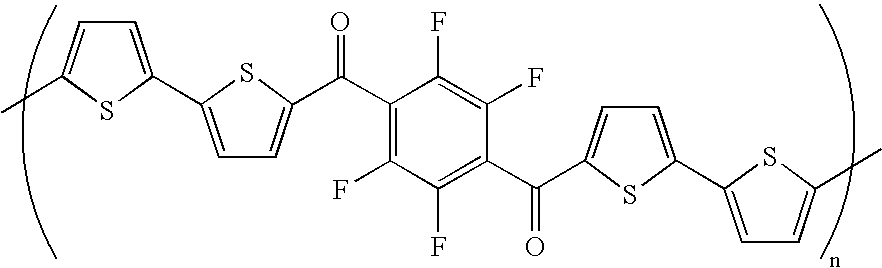
wherein R1, R2 and R3 can be independently selected from H, alkyl, fluorosubstituted alkyl, aryl heterocyclic, and fluorosubstituted aryl moieties, said alkyl and fluorosubstituted alkyl moieties ranging from about C2 to about C10; each said Ar can be an aryl moiety independently selected from phenyl, perfluorophenyl, diacylphenyl, diacylperfluorophenyl, and thiophenyl moieties; each said x can be an integer independently selected from 0 to about 4; y and y′ can be integers independently selected from 0 to about 4; z can be an integer selected from 0 to about 8; and a can be an integer ranging from 0 to about 4, wherein at least one of said x, z and a is selected from 2 and integers greater than 2; and each said w is an integer selected from 0 and 1; and further, R2 can be independently selected from C(O)R1. - Without limitation, in certain embodiments, each of x can be 2, R1 and R2 can be H, y can be 1, y′, z, w and a can be 0, and Ar can be diacylperfluorophenyl. A corresponding polymer of such a compound can be of a formula
and prepared as discussed more fully below. In certain other embodiments of such compounds/polymers, the 3- and/or 4-positions of one or more thiophenyl moieties can be substituted with alkyl, fluorosubstituted alkyl, and/or fluorosubstituted alkylcarbonyl moieties, such moieties as described above. Likewise, in certain other embodiments, alone or in conjunction with the foregoing, the diacyl moiety can, in the alternative, be phenyl or substituted at one or more positions with one or more other halogen moieties. Such compounds can be used as described below, alone or in combination with one or more other compounds of this invention, in the fabrication of OFET devices—including those comprising semiconductor components comprising one or more of the inventive compounds exhibiting hole mobility, electron mobility, or both under operating conditions. - The present invention relates to novel classes of thiophene-based materials substituted with one or more carbonyl moieties on the periphery, on the terminal or lateral positions, and at positions along the oligo/polythiophene backbone. With reference to
Scheme 1, the choice of any carbonyl moiety of the sort described herein, or understood by those skilled in the art made aware of this invention, can be considered for any one of the following reasons: 1) it is one of the strongest electron-withdrawing groups (EWG), 2) in contrast to e.g., CN and NO2 groups, such a moiety allows additional synthetic modifications/functionalization, 3) it can be part of the n-conjugated core, and 4) it prevents β-elimination of fluorine atoms when positioned in between a fluoroalkyl chain and a carbanion site.
Scheme 1. Effect of Carbonyl Substitution/Insertion. - The compounds of this invention have been characterized by a combination of techniques including thermal analysis (DSC, TGA), molecular spectroscopy (NMR, UV-Vis, PL), and electrochemistry (CV, DPP). Results confirm that all the thiophene-carbonyl modified systems are more chemically and thermally stable than the corresponding π-isoelectronic olgothiophenes and are highly volatile and soluble in common organic solvents.
FIG. 2 shows optical spectrum of THF solution and vacuum-deposited films. These data demonstrate that carbonyl-insertion allows for an effective modulation of optical absorption-emission maximum, optical gap, and photoluminescent efficiencies (quantum yields) both in solution and as thin-deposited films. The effect on the optical spectra is much larger than that found for the corresponding diperfluorohexyl and dihexyl carbonyl-free systems, DFH-4T and DH-4T, whose UV-Vis/PL spectra are almost superimposable. - Table 1 summarizes for purposes of comparison and illustration, the electrochemical data of compounds Ia and Ib to that for the corresponding non-carbonyl compounds of the prior art, DFH-4T and DH-4T. The reduction potential values decease of about 0.7-0.9 V. Reversible oxidation potentials were not observed for the carbonyl series, possibly but without limitation because of the low cation stability.
TABLE 1 Electrochemical data (vs. SCE) for the investigate oligothiophenes. Reduction Cathodic Anodic Half Compound Ec1 Ec2 Ea1 Ea2 E1/2 1 E1/2 2 DFH-4T −1.58 −1.82 −1.49 −1.69 −1.53 −1.75 DH-4T −2.01 −2.35 −1.89 −2.24 −1.95 −2.29 DFHCO-4T −0.93 −1.04 −0.83 −0.97 −0.88 −1.01 DHCO-4T −1.19 −1.52 −0.93 −1.42 −1.06 −1.47 - By combining such electrochemical and optical data, absolute orbital energies can be estimated. LUMO energies can be determined from the first reduction potentials and HOMO energies considering the optical gap. As further shown below, modification of an all-thiophene framework by introduction of powerful carbonyl-containing electron-withdrawing groups was found to decrease MO energy levels, allowing for an easier electron injection. The impact of substitution on the morphology of corresponding thin films and single crystals of several compounds was examined by X-ray crystallography. Depending on chemical nature of the system, deposition method (evaporation, spin-coating, casing), substrate temperature and pretreatment, either highly ordered or amorphous solids can be produced and incorporated into various semi-conductor components and related device structures.
- More specifically, several new quaterthiophenes were synthesized according to
Scheme 3 and examples 10, 10a-10i, and characterized by conventional chemical and physical methods.
- With reference to examples 10a-10i, cyclic voltammetry (Versus Fc+/Fc (0.54 vs. SCE/THF) using 0.1 M TBAPF6 electrolyte), of 1-3 in THF reveals two reversible one-electron reduction processes [E1/E2 (V): DHCO-4T −1.06/−1.47; DFHCO-4T −0.88/−1.01; DFHCO-4TCO −0.65/−0.78], considerably less negative than unsubstituted α4T (−1.94/−2.07 V). UV-vis/PL data (
FIG. 4 ) indicate that the C═O groups are effectively conjugated with the 4T core, and exhibit substantially red-shifted absorption/emission maxima [λabs/λem (nm): DHCO-4T 430/530; DFHCO-4T 465/550; DFHCO-4TCO 545/615] and HOMO-LUMO gap reductions [Eg (eV): DHCO-4T 2.6; DFHCO-4T 2.4; DFHCO-4TCO 2.2] vs. 4T [λabs/λem=391/450 m-n, Eg=2.8 eV]. From the electrochemical/optical data HOMO/LUMO energies [EHOMO/ELUMO (eV)] are estimated as follows for DHCO-4T (−6.38/−3.78), DFHCO-4T (−6.36/−3.96) and DFHCO-4TCO (−6.39/−4.19) vs. α4T (EHOMO/ELUMO=−5.79/−2.90 eV). Note that compared to p-type α4T, the new systems exhibit a considerably larger depression of LUMO (˜0.9-1.3 eV) vs. HOMO (˜0.6 eV) energies, suggesting that carbonyl functionalization of the core should more affect electron than hole transport. In contrast, on going from α4T to DFH-4T (EHOMO/ELUMO=−6.19/−3.31 eV) or DH-4T (EHOMO/ELUMO=−5.80/−2.89 eV) a uniform EHOMO/ELUMO shift is observed in agreement with σ-EWD substituent effects. Theoretical and experimental studies on carbonyl-functionalized (oligo)heteroaromatics indicate that HOMO energies are less affected than LUMO's, since the latter are more localized on the molecular core. In marked contrast, the LUMO fully extends to the C═O groups via Sthiophene→C═O intramolecular charge transfer, enhancing substituent σ/π-EWD effects. Therefore, greater perturbation of the 1-3 LUMOs is expected, in excellent agreement with the present electrochemical and optical data. - Such carbonyl-substituted oligothiophenes are thermally stable and undergo quantitative sublimation. Thin films are readily grown from the vapor phase under vacuum and have been characterized by XRD (revealing molecular edge-on-substrate growth orientation), scanning electron microscopy, and FET I-V measurements. Top-contact FET devices were fabricated as described in the literature and elsewhere herein. Briefly, with respect to examples 10a-10i and 11, semiconductors 1-3 (˜50 nm) were vapor-deposited on HMDS-treated p-doped Si/SiO2 substrates maintained at temperatures (TD) between 25-90° C. OFET fabrication was completed by vapor-depositing source-drain Au contacts (˜50 nm). (See, schematically,
FIG. 5 .) Measurements were performed in air and vacuum (˜10−5 Torr), and the standard saturation FET equation (Eq. 1, below) employed to calculate carrier mobilities. -
FIG. 6 shows typical drain-source current-voltage plots for 1-3-based OFETs under different conditions. All of the new oligothiophenes exhibit very high electron mobilities (μe) in vacuum, with average values as a function of deposition temperature (TD) shown inFIG. 7 . For some devices μe as high as ˜0.65 cm2 V−1s−1 has been measured. Interestingly, DHCO-4T films also exhibit relatively large hole (i.e., p-type) mobilities (μh up to 0.01 cm2 V−1s−1) at all deposition temperatures. Ambipolar transport has been observed previously in blend/bilayers and single component OFETs but with modest figures of merit, large imbalances between μe and μh, and only for narrow TD ranges. DHCO-4T is the first organic conductor exhibiting unoptimized μe/μh values as high as ˜0.1/0.01 cm2 V−1s−1. DFHCO-4T also exhibits ambipolar behavior but only after I2 vapor treatment. More electron-deficient DFHCO-4T and DFHCO-4TCO are air-stable with μe's exhibiting the same TD dependence as in vacuum but with ˜5/10× lower magnitudes. Thus, DFHCO-4TCO-based devices can be cycled many times in air without obvious degradation. From the transfer plots, very high Ion:Ioff ratios are observed for electrons, >107. Maximum current gains for holes is >108 for DHCO-4T. The sub-threshold swings (S), indicating how sharply the devices turn on, are in the 1.3-4.9 V/decade range and turn-on voltages |V0| are ˜5-30 V. - Solution-processable semiconductors are attractive for low-cost printed electronics applications. Toward that goal, it has been shown that dioxolane-protected quaterthiophenes (e.g., 10, in
scheme 3, the precursor of DFHCO-4TCO) exhibit very high solubility in common organic solvents due to reduced π-π core stacking (see crystal structure inFIG. 8 ). Preliminary results, films of 10 can be readily converted to DFHCO-4TCO films by deprotection via H2O—HCl vapor treatment/annealing (FIG. 9 ), affording films with μe˜10−4 cm2 V−1s−1. - The combination of electron (n-type) materials with hole-transporters (p-type), or concurrent function from one or a combination of materials, will enable inexpensive, high throughput organic CMOS fabrication via spin-coating, drop casting, and/or printing—in contrast to traditional approaches which are high cost, low throughput, and not readily scalable. Two primary challenges exist for achieving such properties: (i) obtaining favorable crystal packing while allowing dissolution by certain solvents, (ii) achieving n-type transport via appropriate molecular electronic structure/orbital energetics and low-defect density films.3 Post-deposition film processing and chemistries have been explored to address these issues with mixed results, since high purity and highly regular film morphology are essential. As further discussed, below, the present invention provides a new class of soluble oligothiophenes having high electron/hole mobilities both in solution-cast (e.g., μe˜0.25 cm2V−1s−1) and vapor-deposited (e.g., μe˜0.5 cm2V−1s−1) films with very high current modulation (e.g., Ion:Ioff>105 and 108, respectively). Furthermore, the structure and energetics of these molecular motifs can also be used as models for the synthesis/characteristics of other n-type polythiophenes, in accordance with this invention.
- With reference to examples 13a-13e, below, quaterthiophenes 1 and 2 and
polythiophene 3, therein, were synthesized according to Scheme 4 and characterized by conventional chemical and physical methods. Crystals of 1 and 2 suitable for X-ray diffraction were obtained by sublimation. They both crystallize in a herringbone motif (FIG. 10 ), with the shortest inter-core distance being 3.50 Å (C14-C15) and 3.43Å (C14-C16), respectively. The average dihedral angle between the phenyl substitutent and the adjacent thiophene subunit is ˜53° in 1 and ˜49° in 2. The quaterthiophene core of 2 is more planar than that of 1 with a maximum inter-thiophene torsional angle of ˜4° versus ˜13° in 1. However, the 1 carbonyl groups lie ˜6° out of the plane of the adjacent thiophene ring while in 2 this angle increases considerably to ˜17°. - Both semiconductors are thermally stable and undergo quantative sublimation at reduced pressure as indicated by differential scanning calorimetry and thermogravimetric analysis. Films can be grown from the vapor phase and by solution casting from common solvents such as thiophene, toluene, and xylenes. Wide angle x-ray diffraction (WAXRD) indicates that vapor-deposited films are highly crystalline, having the same phase observed in the crystal structure (
FIG. 11 ). The progression of Bragg reflections corresponds to a d-spacing of 27.62 Å(1) and 26.87 Å(2). These spacings are consistent with half of the unit cell long axis (shown inFIG. 10 ), indicating an end-on-substrate molecular orientation, favorable for in-plane charge transport. As the substrate temperature during vapor phase film deposition (TD) is increased from 25 to 90° C., the films become more crystalline and minority crystallite orientations, present at lower TD, are no longer observable by WAXRD. Diffraction patterns similar to the high TD vapor-deposited films are also observed for solution deposited films of 1 (FIG. 12 ). - As described elsewhere, herein, field effect transistors of 1, 2, and 3 were fabricated with Au top-contact electrodes. Semiconductor films (50 nm) were deposited onto temperature controlled HMDS-treated SiO2/p+—Si substrates by vapor deposition and drop casting. A 50 nm layer of Au was then deposited through a shadow mask to define the source and drain electrodes. (See example 14.) OFET characterization was preformed in a high vacuum probe station back-filled with Argon. High electron mobilities (μe) off ˜0.5 cm2V−1s−1 are observed for vapor deposited 1 films (TD=80° C.) with a threshold voltage (VT) of ˜30 V (Ion:Ioff>108,
FIG. 13 ). This highly reproducible μe value is one of the largest reported to date, doubtless reflecting the favorable crystal packing of this molecule. In solution cast devices, μe is exceptionally high with a maximum of ˜0.25 cm2V−1s−1 (Ion:Ioff=105; VT=50-70 V,FIG. 14 ). This is the highest OFET electron mobility for a solution cast semiconductor reported to date, surpassing that of the highest mobility n-type molecular1n (0.01 cm2V−1s−1) and polymeric (0.1 cm2V−1s−1) solution processable semiconductors. The non-fluorinated system, 2, exhibits hole mobilities (μh) in vapor deposited films up to ˜0.04 cm2V−1s−1 (Ion:Ioff=105; VT˜−20 V,FIG. 15 ), but no electron conduction is been observed. Films of this material drop-cast from xylenes haveμ h3×10−4 cm2V−1 s−1. Similar dependencies of mobility on TD are observed in both semiconductors, consistent with the trend, observed by WAXRD, of increased crystallinity with increasing TD. - Cyclic voltammetry of the semiconductors in THF reveals two reversible single-electron reductions (E1/E2 (V) vs. S.C.E.) at −1.05/−1.16 in 1 and at −0.95/−1.30 in 2. Irreversible oxidative features are observed at +1.07/+1.22 for 1. UV-vis absorption in THF indicates that the optical band gap (Eg) is ˜2.40 eV for 1 and ˜2.46 eV for 2. Surprisingly, E1 of n-
type 1 is slightly more negative (0.1 V) than that of p-type 2. Based upon conventional understanding, redox processes, related to MO energetics, are primary factors in determining majority charge carrier type—therefore, it is surprising that 1 exhibits electron mobility in the solid state, while 2 preferentially conducts holes. Without limitation, an explanation may lie in subtle crystal structure molecular conformational differences—the dihedral angle between the electron-withdrawing carbonyl groups and the thiophene core (intrinsically p-type) is much greater in 2 than in 1. This may be a result of crystal packing forces as the DFT-derived vacuum geometry (FIG. 16 ) indicates that the carbonyl oxygen lies closer in the thiophene plane for both molecules. The resulting greater conjugation in 1 should enhance stabilization of the negatively charged core in the solid-state. Since such packing effects are not present in solution, the molecular geometry and hence the electronic structure/energetics are more similar—in agreement with MO computation and the electrochemistry experiment. - Finally, polymer 3 (scheme 4, example 13e) is found to have good solubility in common solvents and forms high-quality films when spun cast from xylenes. In THF, 3 undergoes a reversible two electron reduction at −1.23 V plus an additional irreversible reduction at −1.60 V and three single electron oxidations at +0.96/+1.13 V (reversible) and +1.40 V. While spin cast films of the neat polymer exhibit μe˜10−6 cm2V−1s−1 (optimization in progress), an initial study revealed that blends of 1 and 3 (500-1000 ppm, 1:1 wt. ratio from xylenes) yield films with a μe of ˜0.01 cm2V−1s−1 (Ion:Ioff=104; VT˜60 V). Such blends are promising for OFET printing since the polymer adjusts solution rheology, while the molecular semiconductor enhances charge transport.
- As discussed above, new carbonyl-functionalized oligo/polythiophenes have been prepared and characterized. A combination of one or more carbonyl substituent(s) affects molecular and solid-state properties and affords materials with unique properties. The results summarized above demonstrate the relationship between connectivity at the molecular level and the collective electro-optical properties of organic solids, and show compounds of this invention, in particular compounds I-V, are extremely useful materials for a range of opto-electronic applications. These materials possess low-lying LUMOs which allow/facilitate electron injection/transport as well as HOMO energies compatible with respectable hole transport. For instance, OFETs fabricated by conventional methods exhibit the largest oligothiophene thin-film μe's found to date and approach the performance of pentacene/SiO2 OFETs.
- The following non-limiting examples and data illustrate various aspects and features relating to the compounds and/or device structures of the present invention, including preparation of n-type thiophene semiconductor compounds, as are available through the synthetic methodologies described herein and by incorporated reference. In comparison with the prior art, the present compounds and related devices provide results and data which are surprising, unexpected and contrary thereto. While the utility of this invention is illustrated through the use of several compounds and related semiconductor components made therefrom, it will be understood by those skilled in the art that comparable results are obtainable with various oligo/poly compounds and/or semiconductor components, as are commensurate with the scope of this invention.
- Generally, 2-Thiophenylaldehyde and 2-bromothiophene are commercially available. The reagent 5,5′-bis(tri-b-butylstannyl)-2,2′-dithiophene was prepared according to the known procedure (Wei, Y.; Yang, Y.; Yeh, J,-M. Chem. Mater. 1996, 8, 2659). With reference to Scheme 2 and examples 2-7, compounds 1-4 are prepared as described below, enroute to the diperfluorohexyl and dihexyl compounds, DFHCO-4T and DHCO-4T, respectively.

- While the synthetic techniques schematically illustrated here are provided with reference to the compounds of examples 1-7, analogous procedures or variations thereof—as provided elsewhere herein—can be used or modified as would be understood by those skilled in the art en route to other carbonyl substituted/functionalized oligo/polythiophenes, in accordance with this invention.
- Perfluorohexyl-thien-2-yl-methanol (1). 1.6 M MeLi (15.9 mL) was added dropwise to a solution of 5-thiophenyl aldehyde (2.80 g, 25.0 mmol) and perfluorohexyliodide (11.73 g, 26.3 g) in dry Et2O (70 mL) at −78° C. with stirring. The mixture was stirred for additional 40 min and quenched with 3N HCl (70 mL). The organic layer was separated, washed with water twice, dried over MgSO4, and concentrated in vacuo. Column chromatography of the residue over silica gel (hexane:ethyl acetate=1:1) yielded 1(6.20 g, 57%).
- Perfluorohexyl-(5-bromothien-2-yl)-methanol (2). Bromine (0.698 g) was added to a solution of 1 (1.80 g, 4.16 mmol) in CH2Cl2 (15 mL). After stirring overnight at room temperature, the mixture was neutralized with saturated aqueous NaHCO3 solution and extracted with CH2Cl2 (3×20 mL). The organic layers were combined, dried over MgSO4, and concentrated in vacuo (1.90 g, 89%).
- 2-Perfluorohexylcarbonyl-5-bromothiophene (3). A CH2Cl2 solution of compound 2 (1.90 g, 3.72 mmol) and activated MnO2 (5 g) was stirred overnight. The mixture was filtered with celite. The filtrate was dried over MgSO4, and the solvent was evaporated in vacuum (1.85 g, 98%).
- 5, 5′″-Diperfluorohexylcarbonyl-2,2′:5′,2″:5″,2′″-quaterhiophene, DFHCO-4T, (Ia). A mixture of compound 3 (1.86 g, 3.66 mmol), 5,5′-bis(tri-b-butylstannyl)-2,2′-dithiophene (1.36 g, 1.83 mmol), and tetrakis(triphenylphosphine)palladium(0) (0.13 g, 0.11 mmol) in dry DMF (10 mL) was deaerated three times with N2. The reaction mixture was stirred overnight at 100. ° C. during which time a precipitate formed. After cooling, the dark red solid was collected by filtration and washed several times with hexane, MeOH. Further purification was achieved by gradient vacuum sublimation (1.22 g, 65%). Elemental Analysis calcd for C30H8F26O2S4 (%): C 35.24, H 0.79, F 48.30; found: C 35.13, H 0.84, F 48.51; MS (EI): m/z (%) 1021.5 (100) [M+].
- 2-Heptanoyl-5-bromothiophene (4). 2-Bromothiophene (1.63 g, 10.0 mmol) and heptanoyl chloride (1.78 g, 12.0 mmol) were dissolved in dry benzene (15 mL) and AlCl3 was added in portions with stirring over 10 min. The resulting dark brown solution was refluxed for 1 hr and left to cool down to room temperature. The mixture was quenched with 2M HCl (15 mL) carefully while stirred. The organic layer was separated, washed with 2M HCl, 2M NaOH, and water, and passed through silica column (d=3 cm, I=8 cm). The solution was dried over MgSO4, and concentrated in vacuo (2.40 g, 87%).
- 5,5′″-Diheptanoyl-2,2′:5′,2″:5″,2′″-quaterhiophene, DHCO-4T, (Ib). A mixture of compound 4 (0.64 g, 2.33 mmol), 5,5′-bis(tri-b-butylstannyl)-2,2′-dithiophene (0.744 g, 1.00 mmol), and tetrakis(triphenylphosphine)palladium(0) (0.07 g, 0.06 mmol) in dry DMF (5 mL) was deaerated three times with N2. The reaction mixture was stirred overnight at 100° C. during which time a precipitate formed. After cooling, the orange solid was collected by filtration and washed several times with hexane, MeOH. The solid was recrystalized in xylene and dried in vacuum oven (120° C.) yielding pure compound (0.36 g, 65%). Elemental Analysis calcd for C30H34O2S4 (%): C 64.94, H 6.18; found: C 64.80, H 6.21; MS (EI): m/z (%) 553.9 (100) [M+].
- In accordance with the preceding and following examples, various other carbonyl-functionalized (e.g., heterocylacyl, etc.) oligothiophene compounds of structures I-IV and/or V can be prepared using synthetic techniques of the sort described in the aforementioned incorporated '914 patent or straight-forward modifications thereof, depending upon choice of reagent or thiophene core, as would be understood by those skilled in the art made aware of this invention.
- Field effect transistor devices were fabricated for compounds of the preceding examples using a top-contact configuration. These semiconductors were vacuum-deposited on top of HMDS-treated Si/SiO2 substrates kept at the temperature (TD) of 25 and 70° C. To show the precision of each measurement, the reported data are an average of at least three devices tested at different area of the semiconductor layer. The electrical measurements were performed under vacuum (˜10−4 Torr).
FIG. 3 shows typical drain-source current/voltage plots of compounds Ia and Ib operating at different gate bias. For the purposes of comparison with other organic FETs, the mobilities were calculated by standard field effect transistor equations. In traditional metal-insulator-semiconductor FETs (MISFETs) there is typically a linear and saturated regime in the IDS vs VDS curves at different VG. At large VDS the current saturates and is given by equation (1)
(I DS)sat=(WC i/2L)μ(V G −V t)2 (1)
where L and W are the device channel length and width, respectively, Ci is the capacitance of the insulator (1×10⁻⁸ F/cm2 for 300 nm SiO2). The mobility and the threshold voltage (Vt) can be calculated from the slope and intercept, respectively, of the linear section of the plot of VG versus (Isd)1/2 (at Vsd=−100 V).FIG. 3 shows I-V electrical characteristics of Ia and Ib. From these data n-type mobilities approaching 0.5 cm2/Vs, current on/off ratio of 106-107, and Vt of ˜20V were obtained. Furthermore, devices of Ib exhibit ambipolar characteristics, meaning that a channel of both electrons and holes can be induced upon applying a positive and negative bias to the gate-source contacts, respectively. - With respect to
Scheme 3, below, and examples 10a-10i and 11, the reagent 2-thiophenylaldehyde and 2-bromothiophene are commercially available. The reagent 5,5′-bis(tri-b-butylstannyl)-2,2′-dithiophene was prepared according to the known procedure (Wei, Y.; Yang, Y.; Yeh, J.-M. Chem. Mater. 1996, 8, 2659). Compound 8 was prepared following a known procedure (Brzezinski, J. Z.; Reynolds, J. R. Synthesis 2002, 8, 1053, respectively).
- Synthesis of 5, 5′″-diheptanoyl-2,2′:5′,2″:5″,2′″-quaterhiophene (DHCO-4T, 1). A mixture of compound 4 (0.64 g, 2.33 mmol), 5,5′-bis(tri-n-butylstannyl)-2,2′-dithiophene (0.744 g, 1.00 mmol), and tetrakis(triphenylphosphine)palladium(0) (0.07 g, 0.06 mmol) in dry DMF (5 mL) was deaerated three times with N2. The reaction mixture was stirred overnight at 100° C. during which time a precipitate formed. After cooling, the orange solid was collected by filtration and washed several times with hexane, then MeOH. The solid was recrystalized from xylene and dried in vacuum oven (120° C.) yielding pure compound (0.36 g, 65%). mp 290° C.; 1H NMR (CD2Cl2) δ 7.60 (d, 2H, 2J=3.6 Hz), 7.25 (d, 2H, 2J=3.6 Hz), 7.19 (d, 2H, 2J=3.6 Hz), 7.16 (d, 2H, 2J=3.6 Hz), 2.85 (t, 4H, 3J=7.6 Hz), 1.72-1.70 (m, 4H), 1.36-1.31 (m, 12H), 0.88 (t, 4H, 3J=6.0 Hz); Anal. Calcd for C30H34O2S4: C 64.94, H 6.18. Found: C 64.80, H 6.21; MS (EI): m/z (%) 553.9 (100) [M+].
- Synthesis of 5,5′″-diperfluorohexylcarbonyl-2,2′:5′,2″:5″, 2′″-quaterhiophene (DFHCO-4T, 2). A mixture of compound 3 (1.86 g, 3.66 mmol), 5,5′-bis(tri-b-butylstannyl)-2,2′-dithiophene (1.36 g, 1.83 mmol), and tetrakis(triphenylphosphine)palladium(0) (0.13 g, 0.11 mmol) in dry DMF (10 mL) was deaerated three times with N2. The reaction mixture was stirred overnight at 100° C. during which time a precipitate formed. After cooling, the dark red solid was collected by filtration and washed several times with hexane, then MeOH. Further purification was achieved by gradient vacuum sublimation (1.22 g, 65%). mp 248. ° C.; 1HNMR (CD2Cl2) 120° C. δ 7.93 (2H), 7.39 (2H), 7.32 (2H), 7.27 (2H); 19FNMR (CD2Cl2) 120° C. δ −79.88 (6F), −113.42 (4F), −120.18 (8F), −121.62 (4F), −124.90 (4F). Anal. Calcd for C30H8F26O2S4: C 35.24, H 0.79, F 48.30. Found: C 35.13, H 0.84, F 48.51; MS (EI): m/z (%) 1021.5 (100) [M+].
- Synthesis of 2, 7-[bis-(5-perfluorohexylcarbonylthien-2-yl)]-4H-cyclopenta[2,1-b:3,4-b′]-dithiophen-4-one (DFHCO-4TCO, 3). Molecule 7 (0.50 g, 0.46 mmol) was dissolved in 75 mL acetic acid while refluxing. After addition of concentrated HCl (2 mL), the solution turned from purple to brown, and a dark green precipitate formed immediately. The reaction was quenched with H2O (20 mL). The solution was then decanted off while warm and the product was collected as a dark green solid (0.45 g). The solid was washed with acetone (2×10 mL) and chloroform (6×10 mL), dried overnight in vacuum oven, and purified by gradient sublimation twice. The pure portion was collected and washed with boiling chloroform (20 mL). The red solution was decanted leaving the product as a black solid. It was washed with chloroform and purified by gradient sublimation (0.265 g, 60% yield): mp 297° C.; Anal. Calcd for C31H6F26O3S4: C 35.51, H 0.58. Found: C 35.40, H 0.71; MS (EI, 70 eV) m/z: calcd (M+) for C31H6F26S4O3, 1048.0; found, 1048.0.
- Synthesis of 2-heptanoyl-5-bromothiophene (4). The reagent of 2-bromothiophene (1.63 g, 10.0 mmol) and heptanolyl chloride (1.78 g, 12.0 mmol) were dissolved in dry benzene (15 mL) and AlCl3 was added in portions with stirring over a period of 10 min. The resulting dark brown solution was refluxed for 1 h and left to cool down to room temperature. The reaction mixture was quenched with 2M HCl (15 mL) while carefully stirring. The organic layer was separated, washed with 2M HCl, 2M NaOH, and water, and passed through silica column (d=3 cm, I=8 cm). The collected solution was dried over MgSO4, and concentrated in vacuo (2.40 g, 87%). 1H NMR (CDCl3): δ 7.44 (d, 1H, 2J=3.8 Hz), 7.10 (d, 1H, 2J=3.8 Hz), 2.81 (t, 2H, 3J=7.4 Hz), 1.74-1.68 (m, 2H), 1.38-1.23 (m, 6H), 0.89 (t, 3H, 3J=6.4 Hz); HRMS (EI, 70 eV) m/z: calcd (M+) for C11H15BrOS, 274.00; found, 274.0016.
- Synthesis of perfluorohexyl-thien-2-yl-methanol (5). MeLi (1.6 M, 15.9 mL) was added dropwise to a solution of 5-thiophenyl aldehyde (2.80 g, 25.0 mmol) and perfluorohexyliode (11.73 g, 26.3 g) in dry Et2O (70 mL) at −78° C. with stirring. The mixture was stirred for additional 40 min and quenched with 3N HCl (70 mL). The organic layer was separated, washed with water twice, dried over MgSO4, filtered, and concentrated in vacuo. Column chromatography of the residue over silica gel (hexane:ethyl acetate=1:1) yielded 5 (6.20 g, 57%). 1HNMR (CDCl3): δ 7.45 (d, 1H, 2J=4.5 Hz), 7.24 (d, 1H, 2J=3.0 Hz), 7.10-7.06 (dd, 1H, J=4.5, 3.8 Hz), 5.54-5.46 (m, 1H), 2.56 (d, 1H, 2J=5.7 Hz); HRMS (EI, 70 eV) m/z: calcd (M+) for C11H5F13OS, 431.99; found, 431.9838.
- Synthesis of perfluorohexyl-(5-bromothien-2-yl)-methanol (6). Bromine (0.698 g, 4.37 mmol) was added to a solution of 1 (1.80 g, 4.16 mmol) in CH2Cl2 (15 mL). After stirring overnight at room temperature, the mixture was neutralized with saturated aqueous NaHCO3 solution and extracted with CH2Cl2 (3×20 mL). The organic layers were combined, dried over MgSO4, filtered, and concentrated in vacuo (1.90 g, 89%). 1H NMR (CDCl3): δ 7.02 (d, 1H, 2J=3.7 Hz), 6.97 (d, 1H, 2J=3.8 Hz), 5.46-5.38 (m, 1H), 2.64 (d, 1H, 2J=5.2 Hz); HRMS (EI, 70 eV) m/z: calcd (M+) for C11H4F13BrOS, 509.90; found, 509.8945.
- Synthesis of 2-perfluorohexylcarbonyl-5-bromothiophene (7). A solution of compound 2 (1.90 g, 3.72 mmol) and activated MnO2 (5 g) was stirred overnight. The mixture was filtered through Celite. The filtrate was dried over MgSO4, and the solvent evaporated in vacuum (1.85 g, 98%). The mixture was purified by sublimation; mp 27° C.; 1H NMR (CDCl3): δ 7.74 (d, 1H, 2J=3.8. Hz), 7.23 (d, 1H, 2J=3.8 Hz); 19F NMR (CDCl3) δ −81.20 (3F), −115.20 (2F), −121.77 (4F), −123.18 (2F), −126.53 (2F); Anal. Calcd for C11H2BrF13OS: C 25.95, H 0.40. Found: C 26.11, H 0.54; MS (EI, 70 eV) m/z: (M+) calcd for C11H2BrF13OS 509.8; found 509.8.
- Synthesis of spiro[4H-cyclopenta[2,1-b:3,4-b′]dithiophene-4,2′-[1,3]dioxolane], 2,6-bis(tri-n-butylstannyl) (9). Spiro[4H-cyclopenta[2,1-b:3,4-b′]dithiophene-4,2′-[1,3]dioxolane] (1.71 g, 7.35 mmol) was dissolved in dry THF (20 mL) under nitrogen and cooled to −78° C. Two equivalents of n-BuLi were added dropwise (5.92 mL, 14.85 mmol) and the reaction mixture stirred for 30 min. The solution was allowed to warm to room temperature and stirred for an additional 1.5 h. The resulting thick brown suspension was cooled again to −78° C. and tri-n-butyltin chloride (4.78 g, 14.7 mmol) was added. The solution was then stirred at room temperature for 4 h. The reaction was quenched with 100 mL H2O and extracted with hexane. The organic layer was washed with H2O (6×50 mL) and dried over MgSO4. After filtration, evaporation of the solvent left a brown oil (5.7 g, 95. % yield): 1H NMR (CDCl3): δ 6.96 (s, 2H), 4.33 (s, 4H), 1.57 (m, 12H), 1.33 (m, 12H), 1.10 (m, 12H), 0.91, (t, 18H, 3J=6.8. Hz); HRMS (ACP1, CH2Cl2) m/z: ((M+H)+) calcd for C35H60S2O2Sn2, 814.4; found, 815.2.
- Synthesis of spiro[4H-cyclopenta[2,1-b:3,4-b′]dithiophene-4,2′-[1,3]dioxolane], 2,6-bis-(5-perfluorohexyl carbonylthien-2-yl) (10). A mixture of compound 6 (2.00 g, 2.46 mmol), compound 3 (2.50 g, 4.91 mmol), and Pd[PPh3]4 (0.193 g, 0.167 mmol) in dry DMF (60 mL) was stirred at 90° C. for 6 h. After 15 min a purple solid precipitated. Filtration of the red solution left the disubstituted product as a dark green solid (2.18 g, 81.04% yield). The solid was washed with ether (3×20 mL) and hexane (3×10 mL), dried overnight in vacuum oven, and purified by gradient sublimation: mp 218° C.; 1H NMR (CDCl3): δ 7.88 (2H), 7.32 (4H), 4.39 (4H); 19F NMR (DMSO) −85.88 (6F), −119.69 (4H), −126.43 (8F), −127.85 (4F), −131.21 (4F); Anal. Calcd for C33H10F26O4S4: C 36.27, H 0.92. Found: C 36.15, H 1.01; MS (EI, 70 eV) m/z: (M+) calcd for C33H10F26S4O4, 1092.4; found 1092.2.
- Device Fabrication and Thin Film Characterization. Prime grade n-doped silicon wafers (100) having 300 nm thermally grown oxide (Process Specialties Inc.) were used as device substrates. They were rinsed with water, methanol, and acetone before film deposition. Trimethylsilyl functionalization of the Si/SiO2 surface was carried out by exposing the silicon wafers to hexamethyldisilazane (HMDS) vapor at room temperature in a closed container under nitrogen overnight. Organic compounds were deposited by either vacuum evaporation (pressures <10−5 Torr) at a growth rate of 0.2-0.3 Ås−1, or by casting films from THF solutions (concentrations 200-400 ppm, 10−4-10−2M). Evaporated films were 500 Å thick (as determined by a calibrated in situ quartz crystal monitor), and solution-cast films were variable and thicker, on the order of microns. For solution depositions, a region of the substrate surface (˜1-2 cm2) was defined using 3M Novec™ EGC-1700 electronic coating (comparable to the previously used 3M FC-722 product) before casting. The room temperature or warm solution was transferred inside the defined area and allowed to evaporate, with no special care taken to avoid dust in the environment (a clean hood is optional). For FET device fabrication, top-contact electrodes (500 Å) were deposited by evaporating gold (pressure <10−5 Torr); channel dimensions were 50/100 μm (L) by 5.0 mm (W). The capacitance of the insulator is 2×10⁻⁸ F/cm2 for 300 nm SiO2. TFT device measurements were carried out in a customized vacuum probe station (8×10⁻⁵ Torr) or in air. Coaxial and/or triaxial shielding was incorporated into Signaton probe stations to minimize the noise level. TFT characterization was performed with a Keithly 6430 subfemtoammeter and a Keithly 2400 source meter, operated by a locally written Labview program and GPIB communication.
- Thin films were analyzed by X-ray film diffractometry (XRD), using standard θ-2θ techniques, with Cu Kα radiation and a monochromator. All θ-2θ scans were calibrated in situ with the reflection of the Si (100) substrates. Films were coated with 3 nm of sputtered Au before analysis by scanning electron microscopy (SEM) using a Hitachi S4500 FE microscope.
- With reference to examples 13a-13e, and 14, and Scheme 4, all reagents were purchased from commercial sources and used without further purification unless otherwise noted. Ether and tetrahydrofuran were distilled from Na/benzophenone, and carbon disulfide was distilled from calcium hydride prior to use. Conventional Schlenk techniques were used and reactions carried out under N2 unless otherwise noted. The reagents 5,5′-bis(tributylstannyl)-2,2′-dithiophene and 4,4′-dioctyl-2,2′-dithiophene were prepared following known procedures (Wei, Y.; Yang, Y.; Yeh, J.-M. Chem. Mater. 1996, 8, 2659).

- (2,3,5,6-tetrafluorophenyl) (5-bromothien-2-yl)methanone. To a mixture of perfluorobenzoyl chloride (2.51 g, 10.9 mmol) and 2-bromothiophene (1.86 g, 11.4 mmol) in carbon disulfide (80 mL), aluminum chloride (2.90 g, 21.8, mmol) was added in portions over 10 min with vigorous mechanical stirring. The reaction mixture turned red and was stirred for 2.5 h before being quenched with water (80 mL). The organics were then separated, the aqueous layer extracted with carbon disulfide (3×50 mL), and the combined organics washed with water (3×100 mL) and dried over MgSO4. After filtration, the organics were concentrated in vacuo and the chromatographed on a silica gel column (hexane:ether=9:1) to yield 1.23 g (32%) green crystals. mp 51-54° C.; 1H NMR (DMSO): δ 7.78 (d, 2H, 3J=3.6 Hz), 7.54 (d, 2H, 3J=4.4 Hz); 19F NMR (DMSO): δ −142.1 (m, 2H), −151.6 (m, 1H), −160.6 (m, 2H) Anal. Calcd for C11H2BrF5OS: C 37.00, H 0.56. Found: C 37.37, H 0.83; MS (EI): m/z (%) 355.8 (92) [M+].
- 5,5′″-bis(perfluorophenylcarbonyl)-2,2′,5′, 2″:5″,2′″-quaterthiophene (DFCO-4T, 1). A mixture of (2,3,5,6-tetrafluorophenyl)(5-bromothien-2-yl)methanone (6) (0.511 g, 1.43 mmol), 5,5′-bis(tributylstannyl)-2,2′-dithiophene (0.532 g, 7.15 mmol), and tetrakis(triphenylphosphine)palladium(0) (0.0250 g, 0.0215 mmol) was degassed with nitrogen three times before 8 mL anhydrous DMF was added. The reaction mixture was heated to 80° C. for 10 h with stirring. A red-brown precipitate formed and upon cooling was collected by filtration, washed with hexanes (3×10 mL) and methanol (3×10 mL). Gradient sublimation (2×) afforded a bright orange crystalline material (0.305 g, 60%) with some crystals suitable for x-ray diffraction. mp 291-294° C.; 1H NMR (DMSO): δ 7.87 (d, 2H, 3J=3.2 Hz), 7.70 (d, 2H, 3J=3.2 Hz), 7.60 (d, 2H, 3J=4.4 Hz), 7.54 (d, 2H, 3J=4.0 Hz); 19F NMR (DMSO): δ −142.3 (m), −152.0 (m), −160.7 (m); Anal. Calcd for C30H8F10O2S4: C 50.14, H 1.12, F 26.11. Found: C 50.00, H 1.30, F 26.11; MS (EI): m/z (%) 717.8 (100) [M+].
- (5-bromothien-2-yl)(phenyl)methanone. To a mixture of benzoyl chloride (2.81 g, 20.0 mmol) and 2-bromothiophene (3.42 g, 21.0 mmol) in carbon disulfide (120 mL) aluminum chloride (5.34 g, 40.0 mmol), was added in portions over 10 min with vigorous magnetic stirring. The reaction was next allowed to stir for 2.5 h before being quenched with 100 mL 1 M HCl (aq). The organics were separated, the aqueous layer extracted with carbon disulfide (3×50 mL), and the combined organics washed with water (3×100 mL) and dried over MgSO4. After filtration, the organics were concentrated in vacuo and the residue chromatographed on a silica gel column (hexane:ether=9:1) to yield 5.14 g (96%) of yellow crystals. mp 41-43° C.; 1H NMR (CDCl3): δ 7.84 (d, 2H, 3J=8.0 Hz), 7.62 (t, 1H, 3J=7.2 Hz), 7.52 (t, 2H, 3J=7.5 Hz), 7.40 (d, 2H, 3J=3.5 Hz), 7.15 (d, 2H, 3J=4.0 Hz).
- 5,5′″-bis(phenylcarbonyl)-2,2′:5′,2″:5″, 2′″-quaterthiophene (DPCO-4T, 2). A mixture of 2-bromo-5-benzoylthiohene (1.07 g, 4.00 mmol), 5,5′-bis(tributylstannyl)-2,2′-dithiophene (1.49 g, 2.00 mmol), and tetrakis(triphenylphosphine)palladium(0) (0.0693 g, 0.0600 mmol) was degassed with nitrogen three times before 20 mL anhydrous DMF was added. The reaction mixture was heated to 80° C. for 15 h with stirring. A deep red precipitate formed and upon cooling and was collected by filtration, then washed with hexanes (3×10 mL) and methanol (3×10 mL). Gradient sublimation (2×) afforded an orange-red crystalline material (0.689 g, 64%) with some crystals suitable for x-ray diffraction. mp 307-310° C.; 1H NMR (DMSO): δ 7.85 (2H), 7.84 (2H), 7.67 (4H), 7.59 (2H), 7.53 (2H), 7.48 (1H), 7.44 (1H); Anal. Calcd for C30H18O2S4: C 66.88, H 3.37. Found: C 66.93, H 3.42; MS (EI): m/z (%) 538.0 (100) [M+].
- P(COFCO-4T) (3). A mixture of 4,4′-dioctyl-5,5′-bis(tributylstannyl)-2,2′-dithiophene (0.969 g, 1.00 mmol), 1,4-bis((5-bromothien-2-yl)carbonyl)-2,3,5,6-tetrafluorobenzene (0.530 g, 1.00 mmol), and tetrakis(triphenylphosphine)palladium(0) (34.7 mg, 0.0300 mmol, 0.03 equiv.) was degassed with nitrogen three times before 10 mL anhydrous DMF was added. The reaction mixture was then heated to 110° C. for an additional 72 h during which time four equal amounts of tetrakis(triphenylphosphine)palladium(0) (34.7 mg, 0.0300 mmol, 0.03 equiv.) were added at intervals of 12 h. After cooling, a red precipitate was isolated by filtration through a 0.45 um filter and washed with methanol (200 mL). The powder was next dissolved in CHCl3, precipitated with methanol, and centrifuged to give black pellets which became translucent red upon drying in a vacuum oven. This process was repeated three times to give 3 (342 mg) as translucent red flakes soluble in toluene, xylenes, trichlorobenzene, thiophene, and THF. This material has a Mw of 15,300 and Mn of 6100 by HT-GPC (140° C., trichlorobenzene, calibrated vs. polystyrene). 1H NMR (CDCl3): δ 7.51 (m, 2H), 7.13 (s, 1H); 19F NMR (CDCl3): δ −138.97 (s), −139.03 (s); 119Sn NMR δ −4.2 (s); Anal. Calcd for C40H40F4O2S4: C 63.46, H 5.33. Found: C 63.20, H 5.44.
- Device Fabrication and Thin Film Characterization. Prime grade p-doped silicon wafers (100) having 300 nm thermally grown oxide (Process Specialties Inc. and Montco Silicon Technologies Inc.) were used as device substrates. They were first rinsed with water, methanol, and acetone before film deposition. Trimethylsilyl functionalization of the Si/SiO2 surface was carried out by exposing the silicon wafers to hexamethyldisilazane (HMDS) vapor at room temperature in a closed container under nitrogen overnight. Organic compounds were deposited by either vacuum evaporation (pressures <10−5 Torr) at a growth rate of 0.2-0.3 Ås−1, or by drop casting films from xylenes solutions (concentrations 200-1000 ppm). Polymer films were spin cast from xylenes or drop cast from a xylenes/triethylamine mixture (7:3 v/v), before being annealed under high vacuum for 1 h at 100° C. Films of polymer and molecule blends were cast from xylenes before annealing under the same conditions. Evaporated films were 500 Å thick (as determined by a calibrated in situ quartz crystal monitor), and solution-cast films were variable and thicker, on the order of microns. For solution depositions, the room temperature or warm solution was transferred onto the temperature controlled substrate and allowed to slowly evaporate, with no special care taken to avoid dust or oxygen in the environment (a clean hood is optional). For FET device fabrication, top-contact electrodes (500 Å) were deposited by evaporating gold (pressure <10−5 Torr); channel dimensions were 50/100 μm (L) by 5.0 mm (W). The capacitance of the insulator is 2×10⁻⁸ F/cm2 for 300 nm SiO2. TFT device measurements were carried out in a customized vacuum probe station pumped down to (8×10⁻⁶ Torr) before being backfilled with Argon or in air. Coaxial and/or triaxial shielding was incorporated into Signatone probe stations to minimize the noise level. TFT characterization was performed with a Keithly 6430 sub-femtoamp meter and a Keithly 2400 source meter, operated by a locally written Labview program and GPIB communication. Thin films were analyzed by wide-angle X-ray film diffractometry (WAXRD) on a Rikagu ATX-G using standard θ-2θ techniques, with Cu Kα radiation and a monochromator. All θ-2θ scans were calibrated in situ with the reflection of the Si (100) substrates.
Claims (28)


Priority Applications (2)
| Application Number | Priority Date | Filing Date | Title |
|---|---|---|---|
| US11/227,559 US7528176B2 (en) | 2004-09-14 | 2005-09-14 | Carbonyl-functionalized thiophene compounds and related device structures |
| US12/432,063 US7964650B2 (en) | 2004-09-14 | 2009-04-29 | Carbonyl-functionalized thiophene compounds and related device structures |
Applications Claiming Priority (2)
| Application Number | Priority Date | Filing Date | Title |
|---|---|---|---|
| US60967804P | 2004-09-14 | 2004-09-14 | |
| US11/227,559 US7528176B2 (en) | 2004-09-14 | 2005-09-14 | Carbonyl-functionalized thiophene compounds and related device structures |
Related Child Applications (1)
| Application Number | Title | Priority Date | Filing Date |
|---|---|---|---|
| US12/432,063 Division US7964650B2 (en) | 2004-09-14 | 2009-04-29 | Carbonyl-functionalized thiophene compounds and related device structures |
Publications (2)
| Publication Number | Publication Date |
|---|---|
| US20060186401A1 true US20060186401A1 (en) | 2006-08-24 |
| US7528176B2 US7528176B2 (en) | 2009-05-05 |
Family
ID=37968075
Family Applications (2)
| Application Number | Title | Priority Date | Filing Date |
|---|---|---|---|
| US11/227,559 Active 2026-11-06 US7528176B2 (en) | 2004-09-14 | 2005-09-14 | Carbonyl-functionalized thiophene compounds and related device structures |
| US12/432,063 Expired - Fee Related US7964650B2 (en) | 2004-09-14 | 2009-04-29 | Carbonyl-functionalized thiophene compounds and related device structures |
Family Applications After (1)
| Application Number | Title | Priority Date | Filing Date |
|---|---|---|---|
| US12/432,063 Expired - Fee Related US7964650B2 (en) | 2004-09-14 | 2009-04-29 | Carbonyl-functionalized thiophene compounds and related device structures |
Country Status (7)
| Country | Link |
|---|---|
| US (2) | US7528176B2 (en) |
| EP (1) | EP1831205A4 (en) |
| JP (1) | JP2008513544A (en) |
| KR (1) | KR20070106976A (en) |
| CN (1) | CN101056873A (en) |
| CA (1) | CA2579407A1 (en) |
| WO (1) | WO2007050049A1 (en) |
Cited By (17)
| Publication number | Priority date | Publication date | Assignee | Title |
|---|---|---|---|---|
| US20060205172A1 (en) * | 2005-03-09 | 2006-09-14 | 3M Innovative Properties Company | Perfluoroether acyl oligothiophene compounds |
| US20060202195A1 (en) * | 2004-12-23 | 2006-09-14 | Marks Tobin J | Siloxane-polymer dielectric compositions and related organic field-effect transistors |
| US20070141747A1 (en) * | 2005-12-16 | 2007-06-21 | Xerox Corporation | Electronic device fabrication process |
| US20070243658A1 (en) * | 2006-04-14 | 2007-10-18 | Katsura Hirai | Production method of crystalline organic semiconductor thin film, organic semiconductor thin film, electronic device, and thin film transistor |
| US20070282094A1 (en) * | 2006-05-11 | 2007-12-06 | Marks Tobin J | Silole-based polymers and semiconductor materials prepared from the same |
| US20080142793A1 (en) * | 2006-11-10 | 2008-06-19 | Tang Ming L | Organic Semiconductors |
| US20080161524A1 (en) * | 2006-11-28 | 2008-07-03 | He Yan | Photopolymer-based dielectric materials and methods of preparation and use thereof |
| US20080161464A1 (en) * | 2006-06-28 | 2008-07-03 | Marks Tobin J | Crosslinked polymeric dielectric materials and methods of manufacturing and use thereof |
| WO2009098254A1 (en) * | 2008-02-05 | 2009-08-13 | Basf Se | SEMICONDUCTOR MATERIALS PREPARED FROM RYLENE-(π-ACCEPTOR) COPOLYMERS |
| US20100171102A1 (en) * | 2007-03-09 | 2010-07-08 | Sumitomo Chemical Company, Limited | Fluorine-containing polycyclic aromatic compound, fluorine-containing polymer, organic thin film and organic thin film device |
| WO2010136385A1 (en) | 2009-05-25 | 2010-12-02 | Basf Se | Crosslinkable dielectrics and methods of preparation and use thereof |
| US20100301314A1 (en) * | 2007-11-30 | 2010-12-02 | Osaka University | Conjugated compound, nitrogenated condensed-ring compound, nitrogenated condensed-ring polymer, organic thin film, and organic thin film element |
| WO2011088343A2 (en) | 2010-01-17 | 2011-07-21 | Polyera Corporation | Dielectric materials and methods of preparation and use thereof |
| US20110215334A1 (en) * | 2008-11-24 | 2011-09-08 | Basf Se | Photocurable polymeric dielectrics and methods of preparation and use thereof |
| WO2012013508A1 (en) | 2010-07-30 | 2012-02-02 | Basf Se | Amphiphilic protein in printed electronics |
| WO2016116552A1 (en) * | 2015-01-21 | 2016-07-28 | Ludwig-Maximilians-Universität München | Terminally keto-substituted oligothiophenes and use thereof in optical signal transmission |
| WO2019144082A1 (en) | 2018-01-19 | 2019-07-25 | Flexterra, Inc. | Organic dielectric materials and devices including them |
Families Citing this family (32)
| Publication number | Priority date | Publication date | Assignee | Title |
|---|---|---|---|---|
| EP1794218B1 (en) * | 2004-10-01 | 2020-05-13 | Merck Patent GmbH | Electronic devices containing organic semi-conductors |
| JP5039998B2 (en) * | 2007-01-15 | 2012-10-03 | ダイキン工業株式会社 | Fluorine-containing thiophene polymer |
| JP5342852B2 (en) * | 2007-11-30 | 2013-11-13 | 国立大学法人大阪大学 | Conjugated compound, organic thin film and organic thin film element using the same |
| KR101555076B1 (en) * | 2008-03-17 | 2015-09-22 | 바스프 에스이 | Substituted oligo- or polythiophenes |
| JP2010209264A (en) * | 2009-03-11 | 2010-09-24 | Sumitomo Chemical Co Ltd | Fluorine-containing polymer and organic thin film using the same |
| US8895963B2 (en) | 2009-05-11 | 2014-11-25 | Dainichiseika Color & Chemicals Mfg. Co., Ltd. | Organic semiconductor material, organic semiconductor thin film, and organic thin-film transistor |
| KR101648072B1 (en) | 2009-07-03 | 2016-08-12 | 삼성전자 주식회사 | Organic semiconductor polymer, and transistor including the same |
| US20140221664A1 (en) | 2011-08-10 | 2014-08-07 | Georgia Tech Research Corporation | Coupled heteroaryl compounds via rearrangement of halogenated heteroaromatics followed by oxidative coupling (electron withdrawing groups) |
| WO2013023106A1 (en) | 2011-08-10 | 2013-02-14 | Georgia Tech Research Corporation | Coupled heteroaryl compounds via rearrangement of halogenated heteroaromatics followed by oxidative coupling (acyl moieties) |
| WO2013023109A1 (en) | 2011-08-10 | 2013-02-14 | Georgia Tech Research Corporation | Coupled heteroaryl compounds via rearrangement of halogenated heteroaromatics followed by oxidative coupling (coupled tricyclic core compounds) |
| WO2013023108A1 (en) | 2011-08-10 | 2013-02-14 | Georgia Tech Research Corporation | Coupled heteroaryl compounds via rearrangement of halogenated heteroaromatics followed by oxidative coupling (heteroarylene spacer moiety) |
| TWI589602B (en) | 2012-02-07 | 2017-07-01 | 飛利斯有限公司 | Photocurable polymeric materials and related electronic devices |
| ITMI20120284A1 (en) | 2012-02-27 | 2013-08-28 | E T C Srl | ELECTROLUMINESCENT ORGANIC AMBIPULAR TRANSISTOR WITH FIELD EFFECT WITH DISTRIBUTED LUMINOUS EMISSION |
| CN105659310B (en) | 2013-08-13 | 2021-02-26 | 飞利斯有限公司 | Optimization of electronic display area |
| WO2015031426A1 (en) | 2013-08-27 | 2015-03-05 | Polyera Corporation | Flexible display and detection of flex state |
| TWI655807B (en) | 2013-08-27 | 2019-04-01 | 飛利斯有限公司 | Attachable device having a flexible electronic component |
| WO2015038684A1 (en) | 2013-09-10 | 2015-03-19 | Polyera Corporation | Attachable article with signaling, split display and messaging features |
| CN104513513B (en) * | 2013-10-04 | 2018-11-06 | 日产化学工业株式会社 | Charge-transporting varnish, charge-transporting film and organic electroluminescent device |
| KR20150040216A (en) * | 2013-10-04 | 2015-04-14 | 닛산 가가쿠 고교 가부시키 가이샤 | Charge-transporting varnish, charge-transporting thin film, and organic electroluminescent device |
| EP3087559B1 (en) | 2013-12-24 | 2021-05-05 | Flexterra, Inc. | Support structures for a flexible electronic component |
| KR20160103072A (en) | 2013-12-24 | 2016-08-31 | 폴리에라 코퍼레이션 | Support structures for a flexible electronic component |
| WO2015100224A1 (en) | 2013-12-24 | 2015-07-02 | Polyera Corporation | Flexible electronic display with user interface based on sensed movements |
| WO2015100333A1 (en) | 2013-12-24 | 2015-07-02 | Polyera Corporation | Support structures for an attachable, two-dimensional flexible electronic device |
| CN103772665B (en) * | 2014-01-23 | 2016-03-23 | 中国科学院化学研究所 | A kind of polythiofuran derivative and preparation method thereof and application |
| US20150227245A1 (en) | 2014-02-10 | 2015-08-13 | Polyera Corporation | Attachable Device with Flexible Electronic Display Orientation Detection |
| KR102311596B1 (en) * | 2014-02-18 | 2021-10-12 | 닛산 가가쿠 가부시키가이샤 | Charge-transporting varnish |
| US10261634B2 (en) | 2014-03-27 | 2019-04-16 | Flexterra, Inc. | Infrared touch system for flexible displays |
| TWI692272B (en) | 2014-05-28 | 2020-04-21 | 美商飛利斯有限公司 | Device with flexible electronic components on multiple surfaces |
| WO2015183567A1 (en) | 2014-05-28 | 2015-12-03 | Polyera Corporation | Low power display updates |
| WO2016138356A1 (en) | 2015-02-26 | 2016-09-01 | Polyera Corporation | Attachable device having a flexible electronic component |
| JP6245577B2 (en) * | 2015-03-10 | 2017-12-13 | 国立大学法人山口大学 | Thiophene compound having ferrocenylthiocarbonyl group |
| US10254795B2 (en) | 2015-05-06 | 2019-04-09 | Flexterra, Inc. | Attachable, flexible display device with flexible tail |
Citations (17)
| Publication number | Priority date | Publication date | Assignee | Title |
|---|---|---|---|---|
| US5834100A (en) * | 1996-06-25 | 1998-11-10 | Northwestern University | Organic light-emitting dioddes and methods for assembly and emission control |
| US6399221B1 (en) * | 1996-06-25 | 2002-06-04 | Northwestern University | Organic light-emitting diodes and methods for assembly and emission control |
| US6585914B2 (en) * | 2000-07-24 | 2003-07-01 | Northwestern University | N-type thiophene semiconductors |
| US6608323B2 (en) * | 2000-07-24 | 2003-08-19 | Northwestern University | n-type thiophene semiconductors |
| US6716995B2 (en) * | 2000-08-17 | 2004-04-06 | Lumera Corporation | Design and synthesis of advanced NLO materials for electro-optic applications |
| US6723394B1 (en) * | 1999-06-21 | 2004-04-20 | Cambridge University Technical Services Limited | Aligned polymers for an organic TFT |
| US6878801B2 (en) * | 1999-03-11 | 2005-04-12 | Japan Science And Technology | Optically active polythiophenes |
| US6913710B2 (en) * | 2002-04-24 | 2005-07-05 | Merck Patent Gmbh | Reactive mesogenic benzodithiophenes |
| US6936190B2 (en) * | 2001-10-15 | 2005-08-30 | Fujitsu Limited | Electrically conductive organic compound and electronic device |
| US6939625B2 (en) * | 1996-06-25 | 2005-09-06 | Nôrthwestern University | Organic light-emitting diodes and methods for assembly and enhanced charge injection |
| US20050234256A1 (en) * | 1996-06-25 | 2005-10-20 | Marks Tobin J | Organic light-emitting diodes and related hole transport compounds |
| US6998068B2 (en) * | 2003-08-15 | 2006-02-14 | 3M Innovative Properties Company | Acene-thiophene semiconductors |
| US7029945B2 (en) * | 2001-12-19 | 2006-04-18 | Merck Patent Gmbh | Organic field effect transistor with an organic dielectric |
| US7057054B2 (en) * | 2001-03-05 | 2006-06-06 | Japan Science And Technology Corporation | Photochromic material |
| US7078536B2 (en) * | 2001-03-14 | 2006-07-18 | Genesoft Pharmaceuticals, Inc. | Charged compounds comprising a nucleic acid binding moiety and uses therefor |
| US7081210B2 (en) * | 2002-04-22 | 2006-07-25 | Konica Minolta Holdings, Inc. | Organic semiconductor composition |
| US20070282094A1 (en) * | 2006-05-11 | 2007-12-06 | Marks Tobin J | Silole-based polymers and semiconductor materials prepared from the same |
Family Cites Families (6)
| Publication number | Priority date | Publication date | Assignee | Title |
|---|---|---|---|---|
| US3642631A (en) * | 1970-11-24 | 1972-02-15 | Us Army | Surstituted bithiophenes |
| JPH04164370A (en) * | 1990-04-13 | 1992-06-10 | Idemitsu Kosan Co Ltd | Thiophene derivative, organic semiconductor composed of the thiophene derivative, semiconductor element using the organic semiconductor, and diode element using the organic semiconductor |
| US5602170A (en) * | 1992-02-19 | 1997-02-11 | Industrial Technology Research Institute | Medicinal thiophene compounds |
| KR0176331B1 (en) * | 1996-05-16 | 1999-04-01 | 박원훈 | Floren based shift copolymer for electroluminescent device and electroluminescent device using same as light emitting material |
| WO1998023269A1 (en) * | 1996-11-26 | 1998-06-04 | Purdue Research Foundation | Polythiophene anti-tumor agents |
| JP2001233872A (en) * | 2000-02-28 | 2001-08-28 | Dainippon Printing Co Ltd | Asymmetric liquid crystalline charge transport material having terthiophene skeleton |
-
2005
- 2005-09-14 KR KR1020077008413A patent/KR20070106976A/en not_active Application Discontinuation
- 2005-09-14 US US11/227,559 patent/US7528176B2/en active Active
- 2005-09-14 CN CNA2005800387812A patent/CN101056873A/en active Pending
- 2005-09-14 CA CA002579407A patent/CA2579407A1/en not_active Abandoned
- 2005-09-14 JP JP2007543027A patent/JP2008513544A/en active Pending
- 2005-09-14 WO PCT/US2005/032833 patent/WO2007050049A1/en active Application Filing
- 2005-09-14 EP EP05820820A patent/EP1831205A4/en not_active Withdrawn
-
2009
- 2009-04-29 US US12/432,063 patent/US7964650B2/en not_active Expired - Fee Related
Patent Citations (19)
| Publication number | Priority date | Publication date | Assignee | Title |
|---|---|---|---|---|
| US5834100A (en) * | 1996-06-25 | 1998-11-10 | Northwestern University | Organic light-emitting dioddes and methods for assembly and emission control |
| US6399221B1 (en) * | 1996-06-25 | 2002-06-04 | Northwestern University | Organic light-emitting diodes and methods for assembly and emission control |
| US20050234256A1 (en) * | 1996-06-25 | 2005-10-20 | Marks Tobin J | Organic light-emitting diodes and related hole transport compounds |
| US6939625B2 (en) * | 1996-06-25 | 2005-09-06 | Nôrthwestern University | Organic light-emitting diodes and methods for assembly and enhanced charge injection |
| US6878801B2 (en) * | 1999-03-11 | 2005-04-12 | Japan Science And Technology | Optically active polythiophenes |
| US6723394B1 (en) * | 1999-06-21 | 2004-04-20 | Cambridge University Technical Services Limited | Aligned polymers for an organic TFT |
| US7374702B2 (en) * | 2000-07-24 | 2008-05-20 | Northwestern University | n-Type thiophene semiconductors |
| US6608323B2 (en) * | 2000-07-24 | 2003-08-19 | Northwestern University | n-type thiophene semiconductors |
| US6585914B2 (en) * | 2000-07-24 | 2003-07-01 | Northwestern University | N-type thiophene semiconductors |
| US6991749B2 (en) * | 2000-07-24 | 2006-01-31 | Northwestern University | n-Type thiophene semiconductors |
| US6716995B2 (en) * | 2000-08-17 | 2004-04-06 | Lumera Corporation | Design and synthesis of advanced NLO materials for electro-optic applications |
| US7057054B2 (en) * | 2001-03-05 | 2006-06-06 | Japan Science And Technology Corporation | Photochromic material |
| US7078536B2 (en) * | 2001-03-14 | 2006-07-18 | Genesoft Pharmaceuticals, Inc. | Charged compounds comprising a nucleic acid binding moiety and uses therefor |
| US6936190B2 (en) * | 2001-10-15 | 2005-08-30 | Fujitsu Limited | Electrically conductive organic compound and electronic device |
| US7029945B2 (en) * | 2001-12-19 | 2006-04-18 | Merck Patent Gmbh | Organic field effect transistor with an organic dielectric |
| US7081210B2 (en) * | 2002-04-22 | 2006-07-25 | Konica Minolta Holdings, Inc. | Organic semiconductor composition |
| US6913710B2 (en) * | 2002-04-24 | 2005-07-05 | Merck Patent Gmbh | Reactive mesogenic benzodithiophenes |
| US6998068B2 (en) * | 2003-08-15 | 2006-02-14 | 3M Innovative Properties Company | Acene-thiophene semiconductors |
| US20070282094A1 (en) * | 2006-05-11 | 2007-12-06 | Marks Tobin J | Silole-based polymers and semiconductor materials prepared from the same |
Cited By (36)
| Publication number | Priority date | Publication date | Assignee | Title |
|---|---|---|---|---|
| US20060202195A1 (en) * | 2004-12-23 | 2006-09-14 | Marks Tobin J | Siloxane-polymer dielectric compositions and related organic field-effect transistors |
| US8093588B2 (en) | 2004-12-23 | 2012-01-10 | Northwestern University | Siloxane-polymer dielectric compositions and related organic field-effect transistors |
| US7605394B2 (en) | 2004-12-23 | 2009-10-20 | Northwestern University | Siloxane-polymer dielectric compositions and related organic field-effect transistors |
| US20060205172A1 (en) * | 2005-03-09 | 2006-09-14 | 3M Innovative Properties Company | Perfluoroether acyl oligothiophene compounds |
| US7211679B2 (en) * | 2005-03-09 | 2007-05-01 | 3M Innovative Properties Company | Perfluoroether acyl oligothiophene compounds |
| US20070141747A1 (en) * | 2005-12-16 | 2007-06-21 | Xerox Corporation | Electronic device fabrication process |
| US7651885B2 (en) * | 2005-12-16 | 2010-01-26 | Xerox Corporation | Electronic device fabrication process |
| US20070243658A1 (en) * | 2006-04-14 | 2007-10-18 | Katsura Hirai | Production method of crystalline organic semiconductor thin film, organic semiconductor thin film, electronic device, and thin film transistor |
| US7605225B2 (en) | 2006-05-11 | 2009-10-20 | Northwestern University | Silole-based polymers and semiconductor materials prepared from the same |
| US20100024883A1 (en) * | 2006-05-11 | 2010-02-04 | Marks Tobin J | Silole-Based Polymers and Semiconductor Materials Prepared from the Same |
| US7816480B2 (en) | 2006-05-11 | 2010-10-19 | Northwestern University | Silole-based polymers and semiconductor materials prepared from the same |
| US20070282094A1 (en) * | 2006-05-11 | 2007-12-06 | Marks Tobin J | Silole-based polymers and semiconductor materials prepared from the same |
| US20080161464A1 (en) * | 2006-06-28 | 2008-07-03 | Marks Tobin J | Crosslinked polymeric dielectric materials and methods of manufacturing and use thereof |
| US8274075B2 (en) | 2006-06-28 | 2012-09-25 | Northwestern University | Crosslinked polymeric dielectric materials and electronic devices incorporating same |
| US20110024729A1 (en) * | 2006-06-28 | 2011-02-03 | Marks Tobin J | Crosslinked Polymeric Dielectric Materials And Electronic Devices Incorporating Same |
| US20080142793A1 (en) * | 2006-11-10 | 2008-06-19 | Tang Ming L | Organic Semiconductors |
| US7981989B2 (en) | 2006-11-28 | 2011-07-19 | Polyera Corporation | Photopolymer-based dielectric materials and methods of preparation and use thereof |
| US20080161524A1 (en) * | 2006-11-28 | 2008-07-03 | He Yan | Photopolymer-based dielectric materials and methods of preparation and use thereof |
| US8338555B2 (en) | 2006-11-28 | 2012-12-25 | Polyera Corporation | Photopolymers and their use in organic thin film transistors |
| US20100171102A1 (en) * | 2007-03-09 | 2010-07-08 | Sumitomo Chemical Company, Limited | Fluorine-containing polycyclic aromatic compound, fluorine-containing polymer, organic thin film and organic thin film device |
| US8378338B2 (en) * | 2007-11-30 | 2013-02-19 | Sumitomo Chemical Company, Limited | Conjugated compound, nitrogenated condensed-ring compound, nitrogenated condensed-ring polymer, organic thin film, and organic thin film element |
| US20100301314A1 (en) * | 2007-11-30 | 2010-12-02 | Osaka University | Conjugated compound, nitrogenated condensed-ring compound, nitrogenated condensed-ring polymer, organic thin film, and organic thin film element |
| WO2009098254A1 (en) * | 2008-02-05 | 2009-08-13 | Basf Se | SEMICONDUCTOR MATERIALS PREPARED FROM RYLENE-(π-ACCEPTOR) COPOLYMERS |
| US9219233B2 (en) | 2008-02-05 | 2015-12-22 | Basf Se | Semiconductor materials prepared from rylene-(π-acceptor)copolymers |
| US20110120558A1 (en) * | 2008-02-05 | 2011-05-26 | Basf Se | Semiconductor materials prepared from rylene-(pi-acceptor)copolymers |
| KR101535696B1 (en) * | 2008-02-05 | 2015-07-09 | 바스프 에스이 | SEMICONDUCTOR MATERIALS PREPARED FROM RYLENE-(π-ACCEPTOR) COPOLYMERS |
| US8937301B2 (en) | 2008-11-24 | 2015-01-20 | Basf Se | Photocurable polymeric dielectrics containing 6-substituted coumarin moieties and methods of preparation and use thereof |
| EP2660889A2 (en) | 2008-11-24 | 2013-11-06 | Basf Se | Photocurable polymeric dielectrics and methods of preparation and use thereof |
| US20110215334A1 (en) * | 2008-11-24 | 2011-09-08 | Basf Se | Photocurable polymeric dielectrics and methods of preparation and use thereof |
| US9923158B2 (en) | 2008-11-24 | 2018-03-20 | Basf Se | Photocurable polymeric dielectrics and methods of preparation and use thereof |
| WO2010136385A1 (en) | 2009-05-25 | 2010-12-02 | Basf Se | Crosslinkable dielectrics and methods of preparation and use thereof |
| US8853820B2 (en) | 2009-05-25 | 2014-10-07 | Basf Se | Crosslinkable dielectrics and methods of preparation and use thereof |
| WO2011088343A2 (en) | 2010-01-17 | 2011-07-21 | Polyera Corporation | Dielectric materials and methods of preparation and use thereof |
| WO2012013508A1 (en) | 2010-07-30 | 2012-02-02 | Basf Se | Amphiphilic protein in printed electronics |
| WO2016116552A1 (en) * | 2015-01-21 | 2016-07-28 | Ludwig-Maximilians-Universität München | Terminally keto-substituted oligothiophenes and use thereof in optical signal transmission |
| WO2019144082A1 (en) | 2018-01-19 | 2019-07-25 | Flexterra, Inc. | Organic dielectric materials and devices including them |
Also Published As
| Publication number | Publication date |
|---|---|
| WO2007050049A1 (en) | 2007-05-03 |
| EP1831205A1 (en) | 2007-09-12 |
| CN101056873A (en) | 2007-10-17 |
| EP1831205A4 (en) | 2010-12-01 |
| US20090267061A1 (en) | 2009-10-29 |
| CA2579407A1 (en) | 2006-03-14 |
| JP2008513544A (en) | 2008-05-01 |
| KR20070106976A (en) | 2007-11-06 |
| US7528176B2 (en) | 2009-05-05 |
| US7964650B2 (en) | 2011-06-21 |
Similar Documents
| Publication | Publication Date | Title |
|---|---|---|
| US7528176B2 (en) | Carbonyl-functionalized thiophene compounds and related device structures | |
| EP2307424B1 (en) | HIGH PERFORMANCE SOLUTION PROCESSABLE SEMINCONDUCTOR BASED ON DITHIENO [2,3-d:2',3'-d']BENZO[1,2-b:4,5-b'] DITHIOPHENE | |
| US6585914B2 (en) | N-type thiophene semiconductors | |
| US8110690B2 (en) | Substituted indolocarbazoles | |
| EP2910556B1 (en) | Novel condensed polycyclic aromatic compound and use thereof | |
| US7731796B2 (en) | Nitrogen semiconductor compound and device fabricated using the same | |
| US9187493B2 (en) | Heterocyclic compound and use thereof | |
| US20100006830A1 (en) | Organic semiconductor compound based on 2,7-bis-(vinyl)[1]benzothieno[3,2-b]benzothiophene, organic semiconductor thin film and transistor using the same and methods of forming the same | |
| KR101443189B1 (en) | Novel Diketopyrrolopyrrole polymers and organic electronic device using the same | |
| EP2411378B1 (en) | Tetrathiafulvalene derivative, and organic film and organic transistor using the same | |
| Shan et al. | Organic field-effect transistors based on biselenophene derivatives as active layers | |
| JP2015199716A (en) | Polycyclic fused ring compound, organic semiconductor material, organic semiconductor device, and organic transistor | |
| Duan et al. | Organic field-effect transistors based on two phenylene–thiophene oligomer derivatives with a biphenyl or fluorene core | |
| US8362464B2 (en) | Organic nanofiber structure based on self-assembled organogel, organic nanofiber transistor using the same, and method of manufacturing the organic nanofiber transistor | |
| Um et al. | High-performance organic semiconductors for thin-film transistors based on 2, 7-divinyl [1] benzothieno [3, 2-b] benzothiophene | |
| Chen et al. | An easily made thienoacene comprising seven fused rings for ambient-stable organic thin film transistors | |
| Cuadrado et al. | Air stable organic semiconductors based on diindolo [3, 2-a: 3′, 2′-c] carbazole | |
| US20100224869A1 (en) | Organic semiconductor material, organic semiconductor structure and organic semiconductor apparatus | |
| TW201529580A (en) | Novel condensed polycycloaromatic compound and use thereof | |
| KR100865703B1 (en) | Organic semiconductor containing arylacetylene group, and Organic thin film transistor | |
| Agustin | Soluble Dithienothiophene (DTT) Derived Small Molecules for Organic Thin Film Transistor (OTFT) Application | |
| Castrillo | Preparation and characterization of p-type organic thin film transistors based on a novel triindole derivative |
Legal Events
| Date | Code | Title | Description |
|---|---|---|---|
| AS | Assignment |
Owner name: NATIONAL SCIENCE FOUNDATION, VIRGINIA Free format text: CONFIRMATORY LICENSE;ASSIGNOR:NORTHWESTERN UNIVERSITY;REEL/FRAME:016886/0050 Effective date: 20051107 |
|
| AS | Assignment |
Owner name: NORTHWESTERN UNIVERSITY, ILLINOIS Free format text: ASSIGNMENT OF ASSIGNORS INTEREST;ASSIGNORS:MARKS, TOBIN J.;FACCHETTI, ANTONIO;REEL/FRAME:017543/0352 Effective date: 20051206 |
|
| AS | Assignment |
Owner name: NAVY, SECRETARY OF THE UNITED STATES OF AMERICA, V Free format text: CONFIRMATORY LICENSE;ASSIGNOR:NORTHWESTERN UNIVERSITY;REEL/FRAME:017569/0145 Effective date: 20051107 |
|
| AS | Assignment |
Owner name: NAVY, SECRETARY OF THE UNITED STATES OF AMERICA, V Free format text: CONFIRMATORY LICENSE;ASSIGNOR:NORTHWESTERN UNIVERSITY;REEL/FRAME:018641/0841 Effective date: 20051102 |
|
| STCF | Information on status: patent grant |
Free format text: PATENTED CASE |
|
| AS | Assignment |
Owner name: SOLVAY NORTH AMERICA INVESTMENTS, LLC, TEXAS Free format text: SECURITY AGREEMENT;ASSIGNOR:POLYERA CORPORATION;REEL/FRAME:026658/0146 Effective date: 20110715 |
|
| AS | Assignment |
Owner name: POLYERA CORPORATION, ILLINOIS Free format text: RELEASE BY SECURED PARTY;ASSIGNOR:SOLVAY NORTH AMERICA INVESTMENTS, LLC;REEL/FRAME:028323/0253 Effective date: 20120401 |
|
| FPAY | Fee payment |
Year of fee payment: 4 |
|
| FPAY | Fee payment |
Year of fee payment: 8 |
|
| FEPP | Fee payment procedure |
Free format text: ENTITY STATUS SET TO SMALL (ORIGINAL EVENT CODE: SMAL); ENTITY STATUS OF PATENT OWNER: SMALL ENTITY |
|
| MAFP | Maintenance fee payment |
Free format text: PAYMENT OF MAINTENANCE FEE, 12TH YR, SMALL ENTITY (ORIGINAL EVENT CODE: M2553); ENTITY STATUS OF PATENT OWNER: SMALL ENTITY Year of fee payment: 12 |