US20060247404A1 - Apparatus, precursors and deposition methods for silicon-containing materials - Google Patents
Apparatus, precursors and deposition methods for silicon-containing materials Download PDFInfo
- Publication number
- US20060247404A1 US20060247404A1 US11/117,988 US11798805A US2006247404A1 US 20060247404 A1 US20060247404 A1 US 20060247404A1 US 11798805 A US11798805 A US 11798805A US 2006247404 A1 US2006247404 A1 US 2006247404A1
- Authority
- US
- United States
- Prior art keywords
- porogen
- containing film
- film
- group
- precursor
- Prior art date
- Legal status (The legal status is an assumption and is not a legal conclusion. Google has not performed a legal analysis and makes no representation as to the accuracy of the status listed.)
- Granted
Links
- 0 *O[Si]([4*])([5*])C.C.[1*]O[Si](C)(C)O[2*] Chemical compound *O[Si]([4*])([5*])C.C.[1*]O[Si](C)(C)O[2*] 0.000 description 8
- AGLGXCMMSLJCMB-UHFFFAOYSA-N C.CBrC(C)C.CC(C)(C)Br.CC(C)(C)O[Si](Br)(Br)OC(C)(C)C.CO[Si](C)=O Chemical compound C.CBrC(C)C.CC(C)(C)Br.CC(C)(C)O[Si](Br)(Br)OC(C)(C)C.CO[Si](C)=O AGLGXCMMSLJCMB-UHFFFAOYSA-N 0.000 description 1
- HPKRMROUQZCXRH-UHFFFAOYSA-M C.CC(C)(C)Cl.CO[SiH2]C.[H][Si]([H])(Cl)OC(C)(C)C.[V]I Chemical compound C.CC(C)(C)Cl.CO[SiH2]C.[H][Si]([H])(Cl)OC(C)(C)C.[V]I HPKRMROUQZCXRH-UHFFFAOYSA-M 0.000 description 1
- YPFNXIMGLIFNSX-UHFFFAOYSA-N CC(C)(C)O[Si](Br)(Br)OC(C)(C)C.CC(C)(C)O[Si](Cl)(Cl)OC(C)(C)C Chemical compound CC(C)(C)O[Si](Br)(Br)OC(C)(C)C.CC(C)(C)O[Si](Cl)(Cl)OC(C)(C)C YPFNXIMGLIFNSX-UHFFFAOYSA-N 0.000 description 1
- QUGJSAHKNBUABX-UHFFFAOYSA-N [H][Si]([H])(Br)OC(C)(C)C.[H][Si]([H])(Cl)OC(C)(C)C Chemical compound [H][Si]([H])(Br)OC(C)(C)C.[H][Si]([H])(Cl)OC(C)(C)C QUGJSAHKNBUABX-UHFFFAOYSA-N 0.000 description 1
Images


Classifications
-
- C—CHEMISTRY; METALLURGY
- C23—COATING METALLIC MATERIAL; COATING MATERIAL WITH METALLIC MATERIAL; CHEMICAL SURFACE TREATMENT; DIFFUSION TREATMENT OF METALLIC MATERIAL; COATING BY VACUUM EVAPORATION, BY SPUTTERING, BY ION IMPLANTATION OR BY CHEMICAL VAPOUR DEPOSITION, IN GENERAL; INHIBITING CORROSION OF METALLIC MATERIAL OR INCRUSTATION IN GENERAL
- C23C—COATING METALLIC MATERIAL; COATING MATERIAL WITH METALLIC MATERIAL; SURFACE TREATMENT OF METALLIC MATERIAL BY DIFFUSION INTO THE SURFACE, BY CHEMICAL CONVERSION OR SUBSTITUTION; COATING BY VACUUM EVAPORATION, BY SPUTTERING, BY ION IMPLANTATION OR BY CHEMICAL VAPOUR DEPOSITION, IN GENERAL
- C23C16/00—Chemical coating by decomposition of gaseous compounds, without leaving reaction products of surface material in the coating, i.e. chemical vapour deposition [CVD] processes
- C23C16/22—Chemical coating by decomposition of gaseous compounds, without leaving reaction products of surface material in the coating, i.e. chemical vapour deposition [CVD] processes characterised by the deposition of inorganic material, other than metallic material
- C23C16/30—Deposition of compounds, mixtures or solid solutions, e.g. borides, carbides, nitrides
- C23C16/40—Oxides
- C23C16/401—Oxides containing silicon
-
- C—CHEMISTRY; METALLURGY
- C09—DYES; PAINTS; POLISHES; NATURAL RESINS; ADHESIVES; COMPOSITIONS NOT OTHERWISE PROVIDED FOR; APPLICATIONS OF MATERIALS NOT OTHERWISE PROVIDED FOR
- C09D—COATING COMPOSITIONS, e.g. PAINTS, VARNISHES OR LACQUERS; FILLING PASTES; CHEMICAL PAINT OR INK REMOVERS; INKS; CORRECTING FLUIDS; WOODSTAINS; PASTES OR SOLIDS FOR COLOURING OR PRINTING; USE OF MATERIALS THEREFOR
- C09D183/00—Coating compositions based on macromolecular compounds obtained by reactions forming in the main chain of the macromolecule a linkage containing silicon, with or without sulfur, nitrogen, oxygen, or carbon only; Coating compositions based on derivatives of such polymers
- C09D183/04—Polysiloxanes
-
- C—CHEMISTRY; METALLURGY
- C09—DYES; PAINTS; POLISHES; NATURAL RESINS; ADHESIVES; COMPOSITIONS NOT OTHERWISE PROVIDED FOR; APPLICATIONS OF MATERIALS NOT OTHERWISE PROVIDED FOR
- C09D—COATING COMPOSITIONS, e.g. PAINTS, VARNISHES OR LACQUERS; FILLING PASTES; CHEMICAL PAINT OR INK REMOVERS; INKS; CORRECTING FLUIDS; WOODSTAINS; PASTES OR SOLIDS FOR COLOURING OR PRINTING; USE OF MATERIALS THEREFOR
- C09D4/00—Coating compositions, e.g. paints, varnishes or lacquers, based on organic non-macromolecular compounds having at least one polymerisable carbon-to-carbon unsaturated bond ; Coating compositions, based on monomers of macromolecular compounds of groups C09D183/00 - C09D183/16
-
- Y—GENERAL TAGGING OF NEW TECHNOLOGICAL DEVELOPMENTS; GENERAL TAGGING OF CROSS-SECTIONAL TECHNOLOGIES SPANNING OVER SEVERAL SECTIONS OF THE IPC; TECHNICAL SUBJECTS COVERED BY FORMER USPC CROSS-REFERENCE ART COLLECTIONS [XRACs] AND DIGESTS
- Y10—TECHNICAL SUBJECTS COVERED BY FORMER USPC
- Y10T—TECHNICAL SUBJECTS COVERED BY FORMER US CLASSIFICATION
- Y10T428/00—Stock material or miscellaneous articles
- Y10T428/249921—Web or sheet containing structurally defined element or component
- Y10T428/249953—Composite having voids in a component [e.g., porous, cellular, etc.]
- Y10T428/249967—Inorganic matrix in void-containing component
- Y10T428/249969—Of silicon-containing material [e.g., glass, etc.]
Definitions
- This application relates generally to the deposition of silicon-containing materials in semiconductor and microelectromechanical systems (MEMS) processing. More particularly, this application relates to the production of activated Si precursors and to the polymerization of those precursors to form Si-containing films.
- MEMS microelectromechanical systems
- An aspect provides a method for forming a film, comprising: pyrolyzing a vaporized Si precursor in a first zone to thereby form an activated Si-containing intermediate; transporting the activated Si-containing intermediate to a second zone; and polymerizing the activated Si-containing intermediate in the second zone to thereby form a Si-containing film; the Si precursor being selected from the group consisting of
- X 1 and X 2 are each individually a halogen, deuterium or H;
- X 3 is a halogen;
- R 1 , R 2 and R 3 are each individually selected from the group consisting of —C(CH 3 ) 3 , —C 6 H 5 , and —NR 5 R 6 ;
- R 4 , R 5 and R 6 are each individually selected from the group consisting of hydrogen, deuterium, fluorine, optionally fluorinated C 1 to C 6 alkyl, optionally fluorinated C 1 to C 6 cycloalkyl, optionally fluorinated C 1 to C 6 alkoxy, and optionally fluorinated C 6 to C 10 aryl.
- Another aspect provides a Si-containing film made by such a method.
- Another aspect provides a method for forming a film, comprising: transporting a pyrolyzed Si precursor to a substrate; and polymerizing the pyrolyzed Si precursor in the presence of a porogen to form a Si-containing film on the substrate, the Si-containing film comprising a least a portion of the porogen.
- Another aspect provides a porogen-containing Si-containing film made by such a method.
- Another aspect provides a method for forming a porous film, comprising: transporting a pyrolyzed Si precursor to a substrate; polymerizing the pyrolyzed Si precursor in the presence of a porogen to form a Si-containing polymer; and forming a porous Si-containing film on the substrate, the porous Si-containing film comprising the Si-containing polymer.
- the method comprises depositing the Si-containing polymer and the porogen on the substrate to thereby form a porogen-containing Si-containing film on the substrate; and removing at least a portion of the porogen from the porogen-containing Si-containing film to thereby form the porous Si-containing film.
- Another aspect provides a porous Si-containing film made by such a method.
- thermal transport apparatus comprising a reaction chamber and a storage vessel operably attached to the reaction chamber, the storage vessel being configured to contain at least one reactant source selected from the group consisting of a Si precursor and a porogen;
- the Si precursor being selected from the group consisting of
- X 1 and X 2 are each individually a halogen, deuterium or H;
- X 3 is a halogen
- R 1 , R 2 and R 3 are each individually selected from the group consisting of —C(CH 3 ) 3 , —C 6 H 5 , and —NR 5 R 6 ;
- R 4 , R 5 and R 6 are each individually selected from the group consisting of hydrogen, deuterium, fluorine, optionally fluorinated C 1 to C 6 alkyl, optionally fluorinated C 1 to C 6 cycloalkyl, optionally fluorinated C 1 to C 6 alkoxy, and optionally fluorinated C 6 to C 10 aryl;
- the reaction chamber comprising a hot zone, a transport region downstream of the hot zone, and a polymerization zone downstream of the transport region, the hot zone being configured to accept the reactant source from the storage vessel.
- FIG. 1 illustrates aspects of an embodiment for making a porous Si-containing film.
- FIG. 2 illustrates an embodiment of an apparatus suitable for depositing a Si-containing film.
- FIG. 3 shows FTIR spectra of embodiments of Si-containing films.
- FIG. 4 shows FTIR spectra of embodiments of Si-containing films.
- FIG. 5 shows FTIR spectra of embodiments of Si-containing films.
- FIG. 6 shows an FTIR spectrum of an embodiment of a Si-containing film.
- FIG. 7 shows an FTIR spectrum of an embodiment of a Si-containing film.
- FIG. 8 shows an FTIR spectrum of an embodiment of a Si-containing film.
- FIG. 9 shows FTIR spectra of embodiments of Si-containing films.
- FIG. 10 shows FTIR spectra of embodiments of Si-containing films.
- FIG. 11 shows a scanning electron micrograph of an embodiment of a porous Si-containing film.
- FIG. 12 shows an FTIR spectrum of an embodiment of a porogen-containing Si-containing film.
- FIG. 13 shows an FTIR spectrum of an embodiment of a porogen-containing Si-containing film.
- FIG. 14 shows an FTIR spectrum of an embodiment of a porous Si-containing film.
- FIG. 15 shows an FTIR spectrum of an embodiment of a Si-containing film.
- FIG. 16 shows an FTIR spectrum of an embodiment of a Si-containing film.
- An embodiment provides a method for making a porous Si-containing film.
- the preferred embodiments involve forming a pyrolyzed Si precursor, transporting the pyrolyzed Si precursor to a substrate, polymerizing the pyrolyzed Si precursor in the presence of a porogen to form a porogen-containing Si-containing film on the substrate; and removing the porogen from the Si-containing film to thereby form a porous Si-containing film.
- FIG. 1 schematically illustrates an embodiment.
- FIG. 1 illustrates in general terms a method that begins with a Si precursor of the formula (I):
- X 1 and X 2 are preferably each individually a halogen, deuterium or H; and R 1 and R 2 are each individually selected from the group consisting of —C(CH 3 ) 3 , —C 6 H 5 , and —NR 5 R 6 ; where R 5 and R 6 are each individually selected from the group consisting of hydrogen, deuterium, fluorine, optionally fluorinated C 1 to C 6 alkyl, optionally fluorinated C 1 to C 6 cycloalkyl, optionally fluorinated C 1 to C 6 alkoxy, and optionally fluorinated C 6 to C 10 aryl.
- FIG. 1 illustrates pyrolyzing the Si precursor (I) to form an activated Si-containing intermediate represented by “SiO x *”.
- the activated Si-containing intermediate represented by SiO x * is a Si-containing fragment of the Si precursor (I) in which x is typically in the range of about 1 to 2.
- the SiO x * intermediate is “activated” in the sense that it is capable of polymerizing to form a largely inorganic polymer that comprises a network of silicon and oxygen atoms as discussed in greater detail below.
- SiO x * SiO 2 *
- SiO* SiH 2 O*
- activated Si-containing intermediate pyrolyzed Si precursor
- FIG. 1 further illustrates transporting the SiO x * in the gas or vapor phase to the vicinity of a substrate 105 .
- a porogen 110 is also present in the vicinity of the substrate 105 .
- Polymerization of the SiO x * in the presence of the porogen 110 results in the formation of a Si-containing film 115 a on the substrate 105 , the Si-containing film 115 a trapping at least a portion of the porogen 110 therein.
- FIG. 1 further illustrates removing the porogen 110 from the film 115 a to thereby form a porous Si-containing film 115 b .
- the porous film 115 b comprises pores 120 that were previously occupied by the porogen 110 .
- FIG. 1 Having illustrated an embodiment in general terms in FIG. 1 , a number of aspects, embodiments and variants will now be described in greater detail. It will be appreciated that the aspects, embodiments and variants described below may be practiced separately from one another or in various combinations with one another, e.g., as generally illustrated in FIG. 1 .
- An embodiment provides a method for forming a film that includes pyrolyzing a vaporized Si precursor in a first zone to thereby form an activated Si-containing intermediate, transporting the activated Si-containing intermediate to a second zone, and polymerizing the activated Si-containing intermediate in the second zone to thereby form a Si-containing film.
- the pyrolyzing, transporting and polymerizing steps may be accomplished in various ways, including by thermal transport polymerization (“TP”), see, e.g., U.S. Patent Publication No. 2003/0051662 A1 and U.S. Pat. No. 6,534,616, both of which are hereby incorporated by reference and particularly for the purpose of described thermal TP.
- the Si precursor is selected from the group consisting of a Si precursor of the formula (I) and a Si precursor of the formula (II):
- X 1 and X 2 are each individually a halogen, deuterium or H;
- X 3 is a halogen;
- R 1 , R 2 and R 3 are each individually selected from the group consisting of —C(CH 3 ) 3 , —C 6 H 5 , and —NR 5 R 6 ;
- R 4 , R 5 and R 6 are each individually selected from the group consisting of hydrogen, deuterium, fluorine, optionally fluorinated C 1 to C 6 alkyl, optionally fluorinated C 1 to C 6 cycloalkyl, optionally fluorinated C 1 to C 6 alkoxy, and optionally fluorinated C 6 to C 10 aryl.
- FIG. 2 illustrates an apparatus 200 suitable for pyrolyzing a vaporized Si precursor to form an activated Si-containing intermediate (e.g., as represented by SiO x * in FIG. 1 ), transporting the activated Si-containing intermediate, and polymerizing the activated Si-containing intermediate to form a Si-containing film.
- the apparatus 200 illustrated in FIG. 2 includes a Si precursor 205 in a storage vessel 210 .
- the Si precursor 205 comprises bis-tertiarybutoxy dibromosilane.
- a second vessel 215 contains a nitrogen carrier gas; other carrier gases such as helium, argon, and/or neon may also be suitable.
- a feed line 216 equipped with a valve 217 connects the second vessel 215 to the vessel 210 .
- the vessel 210 is a bubbler 218 by which, during operation, the nitrogen carrier gas supplied by the feed line 216 bubbles through the Si precursor 205 in the storage vessel 210 , thereby vaporizing the Si precursor 205 to form a vaporized Si precursor.
- a feed line 220 equipped with a valve 222 connects the storage vessel 210 to a reaction chamber 225 .
- the bubbler configuration illustrated in FIG. 2 for the supply of the Si precursor 205 is optional and may be omitted as desired, e.g., when the Si precursor 205 has a vapor pressure that is sufficiently high that suitable growth rates may be achieved by, e.g., direct draw of the Si precursor 205 into the reaction chamber 225 .
- the storage vessel 210 is equipped with a heater, and the vaporization of the Si precursor 205 in the storage vessel 210 is controlled by manipulating the amount of heat supplied to the storage vessel 210 by the heater.
- the partial pressure of the Si precursor 205 in the reaction chamber 225 is controlled by manipulating the vacuum applied to the chamber 225 and the temperature of the Si precursor 205 in the storage vessel 210 , without using a carrier gas.
- the reaction chamber 225 is equipped with a heater 230 proximal to the feed line 220 . During operation, the heater 230 heats the reaction chamber 225 , thereby defining a hot zone 235 of the reaction chamber 225 .
- the reaction chamber 225 comprises a substrate 240 and a substrate holder 242 situated within a cool zone 245 of the reaction chamber 225 distal to the feed line 220 , the cool zone 245 being spaced from the hot zone 235 .
- the substrate holder 242 contains internal channels configured to circulate a cooling fluid through feed lines 244 a , 244 b from a temperature control unit 243 , for the purpose of controlling the temperature of the substrate holder 242 and the substrate 240 during operation. While depicted as having separate hot and cool zones within the same reaction chamber, the skilled artisan will appreciate that separate pyrolyzation and deposition chambers can alternatively be provided.
- the vaporized Si precursor (e.g., formed in the vessel 210 by direct draw or by bubbling nitrogen through the Si precursor 205 ) passes through the feed line 220 (via the valve 222 ) and into the hot zone 235 of the reaction chamber 225 .
- the heater 230 heats the reaction chamber 225 to produce a temperature in the hot zone 235 that is effective to pyrolyze the vaporized Si precursor, thereby producing an activated Si-containing intermediate.
- the temperature in the hot zone 235 is about 725° C. In other embodiments, the temperature in the hot zone is preferably in the range of about 500° C.
- the flow of the nitrogen carrier gas transports the activated Si-containing intermediate to the cool zone 245 .
- the temperature of the substrate 240 in the cool zone 245 is effective to polymerize the activated Si-containing intermediate onto the substrate 240 to form a Si-containing film 250 .
- the temperature of the substrate 240 in the cool zone 245 is maintained at about 50° C. by circulating a cooling fluid through the substrate holder 242 using the temperature control unit 243 and the cooling fluid lines 244 a , 244 b .
- the temperature control unit 243 is part of an open loop system, e.g., a system in which the temperature control unit 243 comprises a source of cool water that is fed into the substrate holder 242 through the cooling fluid line 244 a and drains from the substrate holder 242 through the cooling fluid line 244 b .
- the temperature control unit 243 is part of a closed loop system, e.g., a system in which the temperature control unit 243 comprises a refrigeration/pump unit that cools and circulates a cooling fluid such as ethylene glycol from the temperature control unit 243 , through the cooling fluid line 244 a , the substrate holder 242 , and the cooling fluid line 244 b back to the temperature control unit 243 .
- the temperature control unit 243 is equipped with a thermostatic control unit (not shown) to facilitate selection and control of the temperature of the substrate 240 .
- Suitable open loop and closed loop cooling units are known to those skilled in the art and may be obtained from commercial sources.
- the substrate 240 is cooled, rather than the walls of the reaction chamber 225 , to facilitate deposition of the Si-containing film 250 on the substrate 240 and to minimize deposition on the walls of the reaction chamber 225 .
- the walls of the reaction chamber 225 are heated to minimize deposition on the walls.
- the temperature control unit 243 may also be used to heat the substrate 240 , in which case a heating fluid is circulated through the fluid line 244 a , the substrate holder 242 , and the fluid line 244 b in the same general manner as described above.
- Heating of the substrate 240 may be appropriate in various circumstances, e.g., to minimize deposition of undesirable by-products, to maintain the temperature of the substrate 240 above the melting point of a porogen, and/or to remove a porogen from a porogen-containing film deposited on the substrate (discussed below).
- the difference in temperature between the hot zone and the cool zone is at least about 100° C., more preferably at least about 300° C., even more preferably at least about 500° C.
- FIG. 2 further illustrates that the reaction chamber 225 is equipped with an exhaust line 255 proximal to the cool zone 245 .
- the exhaust line 255 is operably attached to a cold trap 260 .
- the cold trap 260 is cooled in liquid nitrogen 262 ; other coolants and cooling configurations may also be used.
- the cold trap 260 is equipped with an outlet 265 that leads to a vacuum pump 270 .
- the outlet 265 is equipped with a valve 267 to control the amount of vacuum applied to the outlet 265 .
- uncondensed by-products flow from the cool zone 245 into the exhaust line 255 and the cold trap 260 .
- Condensable by-products 264 are collected in the trap 260 and thus are prevented from entering the vacuum pump 270 .
- Use of the vacuum pump 270 to apply reduced pressure to the outlet 265 facilitates flow of the vaporized Si precursor, activated Si-containing intermediate, and by-products (and, optionally, carrier gas) through the apparatus 200 .
- the vacuum pump 270 is a diffusion pump capable of applying a vacuum of about 1 ⁇ 10 ⁇ 5 Torr to the outlet 265 .
- Si precursors of the formula (I) include bis-tertiarybutoxy dibromosilane of the formula (III) and bis-tertiarybutoxy dichlorosilane of the formula (IV):
- deposition using Si precursor (III) produces a Si-containing film that comprises —(SiO 2 )— recurring units and a by-product that comprises Br—C(CH 3 ) 3 as illustrated in Scheme (A):
- Si precursors of the formula (I) may be used to form Si-containing films in a manner similar to that illustrated in Scheme (A).
- By-products of such polymerizations preferably comprise R 1 X 1 , R 1 X 2 , R 2 X 1 , and R 2 X 2 .
- Mixtures comprising two or more Si precursors of the formulas (I) and/or (II) may also be used.
- SiO 2 * in Scheme (A) represents various molecular fragments in which the ratio of silicon to oxygen may vary from fragment to fragment, and thus use of “SiO 2 *” does not imply a particular stoichiometry for all such fragments.
- Si precursors of the formula (II) include tertiarybutoxy-bromosilane of the formula (V) and tertiarybutoxy-chlorosilane of the formula (VI):
- deposition using Si precursor (VI) produces a Si-containing film that comprises —(SiH 2 O)— recurring units and Cl—C(CH 3 ) 3 as a by-product as illustrated in Scheme (B):
- Si precursors of the formula (II) may be used to form Si-containing films of the general formula —(SiR 4 R 5 O)— in a manner similar to that illustrated in Scheme (B).
- By-products of such polymerizations preferably comprise R 3 X 3 .
- X 3 is fluorine and neither R 4 nor R 5 are fluorine.
- Mixtures comprising two or more Si precursors of the formulas (I) and/or (II) may be used to form Si-containing films.
- Si-containing films that comprise recurring units of the general formula —[Si(R 4 R 5 )O]-[Si(R 4′ R 5′ )O]— may be formed from a mixture that comprises two different Si precursors of the formula (II), where the definitions for R 4, and R 5, are generally the same as those provided above for R 4 and R 5 , respectively, but where R 4 ⁇ R 4′ and/or R 5 ⁇ R 5′ for the two different precursors.
- Si-containing films comprising recurring units of the general formula —(SiO 2 )—(Si(R 4 R 5 )O)— may be formed from a mixture that comprises a Si precursors of the formula (I) and a Si precursor of the formula (II).
- the Si-containing film is crosslinked.
- the —SiO 2 — recurring units may form crosslinks.
- SiH 2 O* in Scheme (B) represents various molecular fragments in which the relative ratios of silicon, oxygen and hydrogen may vary from fragment to fragment, and thus use of “SiH 2 O*” does not imply a particular stoichiometry for all such fragments.
- the temperature for pyrolyzing a Si precursor to form an activated Si-containing intermediate varies, depending on the nature of the Si precursor, and may be identified by routine experimentation in view of the guidance provided herein.
- Pyrolysis temperatures e.g., temperatures in the hot zone 235
- temperatures in the hot zone 235 in the range of about 500° C. to about 850° C., preferably in the range of about 650° to about 750° C., are suitable for a variety of Si precursors of the formulas (I) and (II), although in particular cases higher or lower temperatures may be used.
- the heater 230 preferably heats the reaction chamber 225 to produce a temperature in the hot zone 235 of about 725° C.
- the activated Si-containing intermediate may consist essentially of silicon and oxygen.
- the pyrolysis temperature is preferably effective to result in the removal of R 1 , R 2 , X 1 and X 2 from Si precursor (I).
- the activated Si-containing intermediate may consist essentially of silicon, oxygen, R 4 and R 5 .
- the pyrolysis temperature is preferably effective to result in the removal R 3 and X 3 from Si precursor (II).
- the pyrolysis temperature (e.g., the temperature in the hot zone 235 ) facilitates formation of a volatile by-product that does not undesirably contaminate the Si-containing film (e.g., the Si-containing film 250 that forms on the substrate 240 in the cool zone 245 ).
- the temperature in the hot zone 235 is preferably lower than the temperature at which reactive by-products (e.g., by-products capable of undesirably reacting with the film 250 ) are formed.
- the pyrolysis conditions are preferably controlled so that any reactive by-products react with one another to form relatively non-reactive volatile by-products, e.g., volatile by-products that do not undergo significant or undesirable chemical reactions with the deposited Si-containing film.
- X 1 , X 2 , X 3 , R 1 , R 2 and R 3 are preferably each individually leaving groups capable of reacting with one or more of each other to form a volatile by-product.
- R 3 , R 4 , R 5 , and X 3 are each individually chemical groups selected such that the R 4 —Si and R 5 —Si chemical bonds are more stable during the pyrolyzing of the Si precursor than the X 3 —Si and R 3 —O bonds.
- X 1 and X 2 are each individually a halogen or H; X 3 is a halogen; R 1 , R 2 and R 3 are each individually selected from the group consisting of —C(CH 3 ) 3 , —C 6 H 5 , and —NR 5 R 6 ; and R 4 , R 5 and R 6 are each individually selected from the group consisting of hydrogen, deuterium, fluorine, optionally fluorinated C 1 to C 6 alkyl, optionally fluorinated C 1 to C 6 cycloalkyl, optionally fluorinated C 1 to C 6 alkoxy, and optionally fluorinated C 6 to C 10 aryl.
- R 1 and R 2 are each individually selected from the group consisting of —C(CH 3 ) 3 and —CF 3
- X 1 and X 2 are each individually selected from the group consisting of hydrogen, deuterium, fluorine, methyl, and ethyl.
- a Si-containing film may be formed on a substrate by transporting a pyrolyzed Si precursor to a substrate and polymerizing the pyrolyzed Si precursor.
- Such transport of the pyrolyzed Si precursor is typically from a hot zone (e.g., the hot zone 235 ) through a transport region downstream of the hot zone to a cool zone (e.g., the cool zone 245 ) downstream of the transport region.
- the conditions for transporting the pyrolyzed Si precursor are preferably selected to minimize polymerization of the pyrolyzed Si precursor at the pyrolysis temperature (e.g., in the hot zone 235 ) or in the gas phase (e.g., during transport through the transport region situated between the hot zone 235 and the cool zone 245 ).
- the substrate 240 is preferably maintained at a temperature that is lower than in the transport region between the hot zone 235 and the substrate 240 .
- transport of the pyrolyzed Si precursor is conducted by use of an inert carrier gas to sweep the pyrolyzed Si precursor from a first zone (e.g., the hot zone 235 ) to a second zone (e.g., the cool zone 245 ).
- an inert carrier gas tends to dilute the pyrolyzed Si precursor, thereby reducing the rate of gas phase polymerization among activated Si-containing intermediates, and tends to separate activated Si-containing intermediates from other reactive species (such as reactive by-products), thereby reducing the rate of formation of potential Si-containing film contaminants.
- an inert carrier gas such as N 2 , Ar, Xe, and He
- a reactive carrier gas instead of a reactive carrier gas
- the carrier gas it is preferable for the carrier gas to contain a minor amount of an oxygen source, e.g., to facilitate production of activated Si-containing intermediates that primarily consist of silicon and oxygen and/or to oxidize the deposited Si-containing film.
- suitable oxygen sources include O 2 , O 3 , N 2 O and mixtures thereof.
- polymerization to form a Si-containing film typically occurs spontaneously on a substrate that is at a temperature at which polymerization is thermodynamically favorable.
- the temperature of the substrate e.g., the substrate 240
- the substrate is typically selected to facilitate polymerization and is often in the range of about ⁇ 50° C. to about 300° C., although higher or lower substrate temperatures may be suitable in particular cases.
- the substrate is maintained at a relatively low temperature (e.g., in the range of about ⁇ 25° C. to about 50° C.) to facilitate formation of a Si-containing film that comprises a porogen (discussed in greater detail below) and/or to achieve relatively higher deposition rates.
- the substrate 240 may be cooled by the substrate holder 242 and the temperature control unit 243 as discussed above with respect to FIG. 2 .
- cooling may result in the entrapment of by-products (such as Br—C(CH 3 ) 3 , Scheme (A)) within the Si-containing film and such entrapped by-products may act as porogens
- the temperature of the substrate is preferably selected so that the by-products are relatively volatile, so that little if any of the by-products of pyrolysis or polymerization are entrapped within the Si-containing film.
- the Si-containing film consists essentially of the polymerization product(s) of the activated Si-containing intermediate(s) formed from the Si precursor(s).
- the substrate temperature is selected to be above the boiling temperature of the by-product(s), but below the boiling temperature of the porogen (at the deposition pressure), to facilitate removal of the by-product and incorporation of the porogen. Such embodiments are discussed in greater detail below.
- Pyrolysis, transport and polymerization to form a Si-containing film as described above is preferably conducted in a chamber, e.g., the reaction chamber 225 illustrated in FIG. 2 , although activated Si-containing intermediates may also be transported between separate pyrolysis and polymerization chambers.
- the pressure in the reaction chamber 225 may be controlled by manipulating the partial pressures of the various constituents (e.g., Si precursor, activated Si-containing intermediate, optional carrier gas, optional oxygen source, and optional porogen), the temperatures in the hot zone 235 and the cool zone 245 , and the vacuum applied by the vacuum pump 270 .
- pressures at various stages of the overall process may vary over a broad range from about 1 ⁇ 10 ⁇ 4 Torr to about 7,600 Torr, depending on the nature of the Si precursor and by-product(s), and the structure desired for the resulting Si-containing film (e.g., non-porous, porogen-containing, porous) as described in greater detail below.
- Deposition rates tend to be a function of pressure (and particularly Si precursor partial pressure), and thus relatively higher deposition rates are typically obtained at relatively higher overall pressures and/or relatively higher Si precursor partial pressures.
- higher Si precursor partial pressures may be achieved at lower overall pressures because such lower pressures may lead to increased volatilization of the Si precursor.
- Methods for forming Si-containing films may further comprise various post-deposition film treatments such as annealing and/or oxidizing.
- the as-deposited Si-containing film may be annealed for various reasons, e.g., to reduce stress, to volatilize porogens and/or by-products, and/or to remove or alter undesirable chemical groups. Porogen removal is discussed in greater detail below.
- Annealing temperatures are typically in the range of about 50° C. to about 600° C., preferably in the range of about 150° C. to about 450° C.
- the chamber pressure during annealing is preferably about 600 Torr or less.
- Annealing times are typically in the range of 10 minutes to about 3 hours, preferably in the range of about 30 minutes to two hours.
- Annealing may be conducted in the deposition chamber, e.g., without exposing the as-deposited Si-containing film to ambient, and/or may be conducted by annealing an as-deposited or previously treated film after the film is removed from the deposition chamber, e.g., in a separate anneal station.
- at least a part of the annealing is conducted under an inert gas (e.g., N 2 , He, Ar, Ne).
- at least a part of the annealing is conducted under a gas selected from the group consisting of nitrogen, helium, hydrogen, a nitrogen/helium mixture, and a nitrogen/hydrogen mixture.
- Oxidation of the Si-containing films may be carried out with or without annealing, and may be carried out for various purposes, e.g., to alter and/or remove undesirable chemical groups from the Si-containing films.
- elements such as carbon that may be present in the as-deposited film may be oxidized to form volatile carbon oxides (e.g., CO, CO 2 ) and thereby removed from the film.
- Oxidation of the Si-containing films may be conducted by exposing the Si-containing film to an oxygen-containing gas (e.g., O 2 , O 3 , N 2 O and mixtures thereof), with or without plasma activation, preferably with annealing, either within the deposition chamber after removing the as-deposited or previously treated film from the deposition chamber.
- an oxygen-containing gas e.g., O 2 , O 3 , N 2 O and mixtures thereof
- An embodiment provides a method for forming a film that includes transporting a pyrolyzed Si precursor to a substrate and polymerizing the pyrolyzed Si precursor in the presence of a porogen to form a Si-containing film on the substrate, the Si-containing film comprising at least a portion of the porogen.
- Various suitable methods for making and transporting a pyrolyzed Si precursor to a substrate are discussed above. Polymerization of a pyrolyzed Si precursor in the presence of a porogen to form a porogen-containing Si-containing film is conceptually illustrated in FIG. 1 as discussed above.
- Si-containing film that consists essentially of —(SiO 2 )— recurring units.
- Si-containing film is an amorphous, relatively non-porous material that is chemically and structurally similar to silicon dioxide.
- Si precursor (VI) as illustrated in Scheme (B) produces a pyrolyzed Si precursor represented by SiH 2 O* that primarily consists essentially of silicon, hydrogen and oxygen atoms. Subsequent polymerization of the SiH 2 O* produces a Si-containing film that primarily consists essentially of —SiH 2 )— recurring units.
- a Si-containing film is a relatively non-porous material.
- Other Si precursors of the formula (II) may be pyrolyzed similarly to produce pyrolyzed Si precursors that primarily consist of silicon, oxygen, R 4 and R 5 , and polymerized similarly to form Si-containing films that primarily consist of the same elements as the precursors. In an embodiment, such Si-containing films are also relatively non-porous.
- the porogen 110 becomes entrapped within the polymerization matrix, resulting in the formation of a Si-containing film 115 a that comprises at least a portion of the porogen 110 that is present during the polymerization.
- the porogen 110 is capable of being removed from the film to form a porous film 115 b comprising pores 120 previously occupied by the porogen 110 .
- porogen refers to a substance or mixture of substances that, when present during the polymerization of a pyrolyzed Si precursor to form a Si-containing film, becomes incorporated into the film in such a way as to permit it to be subsequently removed from the film to produce a porous Si-containing film that has greater porosity than an otherwise comparable Si-containing film formed by formed by an otherwise substantially identical process but in the absence of the porogen.
- Porogens preferably have a molecular weight of less than about 1,000 Daltons, to facilitate removal from the film. The porogen may be removed from the film during film deposition, and thus it is not necessary to detect a particular substance within a film in order to conclude that it is a porogen.
- Porogens or portions thereof may become chemically bonded to the film, in which case subsequent removal may involve chemical bond scission.
- at least a portion of the porogen is not chemically bonded to the Si-containing film; more preferably, substantially all of the porogen is not chemically bonded to the Si-containing film.
- porogens examples include optionally halogenated C 2 -C 10 alcohol, optionally halogenated C 2 -C 10 diol, optionally halogenated C 2 -C 10 ether, optionally halogenated C 2 -C 10 ketone, optionally halogenated C 2 -C 10 ester, optionally halogenated C 2 -C 10 aldehyde, optionally halogenated C 1 -C 10 hydrocarbon, optionally halogenated C 2 -C 10 carboxylic acid, optionally halogenated C 2 -C 10 anhydride, carbon monoxide, carbon dioxide, and mixtures thereof.
- preferred porogens include dimethyl oxalate, di-tertiarybutyl oxalate, carbon tetrabromide, benzene, methanol, t-butanol and mixtures thereof.
- FIG. 2 illustrates an apparatus 200 suitable for transporting a pyrolyzed Si precursor to a substrate and polymerizing the pyrolyzed Si precursor in the presence of a porogen to form a porogen-containing Si-containing film on the substrate.
- the apparatus 200 includes a vessel 275 and a feed line 276 running from the vessel 275 to a transport region of the reaction chamber 225 between the hot zone 235 and the cool zone 245 .
- the vessel 275 contains a porogen 280 , which in the illustrated embodiment comprises di-tertiarybutyl oxalate.
- a bubbler configuration similar to that used to supply the Si precursor 205 to the reaction chamber 225 is used to supply the porogen 280 to the reaction chamber 225 .
- another vessel 215 a contains a nitrogen carrier gas; other carrier gases such as helium, argon, and/or neon may also be suitable.
- a feed line 216 a equipped with a valve 217 a connects the vessel 215 a to the vessel 210 .
- the vessel 275 is a bubbler 218 a by which, during operation, the nitrogen carrier gas supplied by the feed line 216 a bubbles through the porogen 280 in the storage vessel 275 , thereby vaporizing the porogen 280 to form a vaporized porogen.
- a feed line 220 a equipped with a valve 222 a connects the storage vessel 275 to the reaction chamber 225 . It will be understood that the bubbler configuration illustrated in FIG.
- the storage vessel 275 is equipped with a heater, and the vaporization of the porogen 280 in the storage vessel 275 is controlled by manipulating the amount of heat supplied to the storage vessel 275 by the heater.
- the partial pressure of the porogen 280 in the reaction chamber 225 is controlled by manipulating the vacuum applied to the chamber 225 and the temperature of the porogen 280 in the storage vessel 275 , without using a carrier gas.
- the porogen 280 enters the reaction chamber 225 via the feed line 220 a and the valve 222 a .
- the porogen 280 flows into the cool zone 245 and into the presence of the pyrolyzed Si precursor at the substrate 240 .
- Polymerization of the pyrolyzed Si precursor to form the Si-containing film 250 on the substrate 240 takes place in the general manner described above, except that at least a portion of the porogen 280 is entrapped within the Si-containing film 250 during the polymerization, thereby forming a Si-containing film that comprises a least a portion of the porogen 280 .
- Methods for forming porogen-containing Si-containing films may further comprise various post-deposition film treatments such as annealing and/or oxidizing.
- the as-deposited porogen-containing Si-containing film may be annealed for various reasons, e.g., to reduce stress, to remove trapped porogens and/or by-products, and/or to remove or alter undesirable chemical groups.
- Annealing temperatures are typically in the range of about 50° C. to about 600° C., preferably in the range of about 150° C. to about 450° C.
- Annealing times are typically in the range of 10 minutes to about 3 hours, preferably in the range of about 30 minutes to two hours.
- Annealing may be conducted in the deposition chamber, e.g., without exposing the as-deposited porogen-containing Si-containing film to ambient, and/or may be conducted by annealing an as-deposited or previously treated film after the film is removed from the deposition chamber in a separate anneal station, with or without exposure to ambient.
- annealing may be accomplished by heating the substrate 240 and the Si-containing film 250 using the temperature control unit 243 .
- the pressure during annealing may be controlled by manipulating the vacuum applied by the vacuum pump 270 via valve 267 .
- the chamber may also be pressurized by filling the reaction chamber 225 with a gas e.g., by attaching a third gas source 285 to the reaction chamber 225 via a valve 287 , using appropriate precautions for dealing with pressurized systems.
- a gas e.g., by attaching a third gas source 285 to the reaction chamber 225 via a valve 287 .
- at least a part of the annealing is conducted under an inert annealing gas (e.g., N 2 , He, Ar, Ne).
- at least a part of the annealing is conducted under an annealing gas selected from the group consisting of nitrogen, helium, hydrogen, a nitrogen/helium mixture, and a nitrogen/hydrogen mixture.
- the third gas source 285 may comprise such an annealing gas or gases.
- Oxidation of the porogen-containing Si-containing films may be carried out with or without annealing, and may be carried out for various purposes, e.g., to alter and/or remove undesirable chemical groups from the Si-containing films and/or to remove the porogen by oxidation.
- oxidation may be preferred in an embodiment in which removal of the porogen by volatilization is difficult or inconvenient and in which the oxidation of the porogen produces oxides having greater volatility.
- Oxidation of the Si-containing films and/or porogens contained therein may be conducted by exposing the porogen-containing Si-containing film to an oxygen-containing gas (e.g., O 2 , O 3 , N 2 O and mixtures thereof), with or without plasma activation, preferably with annealing, either within the deposition chamber after removing the as-deposited or previously treated film from the deposition chamber.
- oxygen-containing gases may comprise the third gas source 285 and thus may be introduced into the reaction chamber 225 via the valve 287 .
- the chamber pressure may be varied over a broad range, e.g., from about 7,600 Torr to about 1 ⁇ 10 ⁇ 4 Torr, depending on the stage of the overall process.
- the pressure during annealing is relatively low to facilitate removal of the porogen, as discussed in greater detail below.
- the pressure during annealing or during an annealing stage is relatively high, e.g. in the range of about 760 Torr to about 7,600 Torr.
- Such pressures may be applied during annealing to minimize or prevent volatilization of an entrapped porogen from a Si-containing film during annealing. For example, prior to removing the porogen, it may be desirable to anneal a porogen-containing Si-containing film to stabilize the structure of the Si-containing film surrounding the porogen.
- Porogen-containing Si-containing films preferably contain an amount of porogen that is effective to produce a porous film (e.g., the film 115 b in FIG. 1 ) having the desired degree of porosity upon removal of the porogen.
- Amounts of porogen in the porogen-containing Si-containing film may vary over a broad range, e.g., form about 0.001% to about 70% by weight, based on total film weight, depending on the application.
- the dielectric constants of porous films generally decrease as the degree of porosity increases, but in many cases the mechanical properties of porous films also tend to decrease as the degree of porosity increases.
- preferred levels of porogen in a particular porogen-containing Si-containing film typically represent a balance between dielectric and mechanical properties, and may be in the range of about 0.01% to about 40%, more preferably about 1% to about 30%, by weight based on total film weight.
- the porogen may be distributed relatively uniformly throughout the film or varied as a function of position within the film.
- the amount of porogen in the porogen-containing Si-containing film is varied as a function of depth in the film.
- One way of making such a graded film is from a similarly graded porogen-containing Si-containing film.
- the amount of porogen incorporated into the porogen-containing Si-containing at any particular film depth is a function of the relative amount of porogen present during the polymerization of the pyrolyzed Si precursor.
- the relative amount of porogen may be controlled in various ways.
- the valve 222 a and/or the flow of the nitrogen carrier gas 215 a may be manipulated during deposition to control the flow of the porogen 280 into the reaction chamber 225 .
- the relative amount of porogen present during polymerization may also be controlled by varying the amount of Si precursor, e.g., by reducing the flow of the Si precursor 215 (e.g., by manipulation of the valve 217 and/or the valve 222 ), thereby increasing the relative amount of the porogen 280 at the substrate 240 , or vice-versa.
- Mass flow controllers MFC's
- the concentration of porogen in the film is graded, e.g., the concentration of porogen is lower near a surface of a porogen-containing Si-containing film as compared to the concentration of porogen near the center of the porogen-containing Si-containing film.
- concentration of porogen in the film is graded, e.g., the concentration of porogen is lower near a surface of a porogen-containing Si-containing film as compared to the concentration of porogen near the center of the porogen-containing Si-containing film.
- An embodiment provides a method for forming a porous film, comprising: transporting a pyrolyzed Si precursor to a substrate; polymerizing the pyrolyzed Si precursor in the presence of a porogen to form a Si-containing polymer; and forming a porous Si-containing film on the substrate, the porous Si-containing film comprising the Si-containing polymer.
- a pyrolyzed Si precursor transporting it to a substrate, and polymerizing it in the presence of a porogen are discussed above. In some embodiments, such polymerization results in the formation of a porous Si-containing film, without the formation of a discrete intermediate porogen-containing Si-containing film.
- the method involves forming a porogen-containing intermediate film 115 a and then removing the porogen 110 to create the porous Si-containing film 115 b .
- the method further comprises depositing the Si-containing polymer and the porogen on the substrate to thereby form the porogen-containing Si-containing film 115 a on the substrate 105 ; and removing at least a portion of the porogen 110 from the porogen-containing Si-containing film 115 a to thereby form the porous Si-containing film 115 b.
- Porogens may be removed in various ways from porogen-containing Si-containing films to form porous Si-containing films. It has been found that a number of factors may affect porogen removal including porogen volatility, time, temperature, pressure, and/or environmental conditions (e.g., presence or absence of water, oxygen, hydrogen, inert gas, etc., during porogen removal). In most cases, removal of the porogen may be accomplished by establishing suitable volatilization conditions, e.g., by manipulating the temperature and pressure applied to the porogen-containing Si-containing film so that the film is at a temperature that is near or above the boiling point or sublimation temperature of the porogen at the applied pressure.
- suitable volatilization conditions e.g., by manipulating the temperature and pressure applied to the porogen-containing Si-containing film so that the film is at a temperature that is near or above the boiling point or sublimation temperature of the porogen at the applied pressure.
- volatilization conditions e.g., temperature and pressure
- Temperatures lower than the boiling or sublimation point of the particular porogen at the applied pressure may be suitable, but result in slower volatilization.
- relatively faster and more complete volatilization is typically achieved by applying relatively higher temperatures and/or lower pressures.
- the porous Si-containing film may be formed in the same chamber as the porogen-containing Si-containing film.
- the as-deposited Si-containing film 250 may be heated for various reasons, e.g., to reduce stress, to volatilize porogens and/or by-products, and/or to remove or alter undesirable chemical groups.
- the Si-containing film 250 comprises a porogen 280
- the porogen 280 may be removed while the Si-containing film 250 remains in the reaction chamber 225 .
- porogen removal may be accomplished by heating the substrate 240 and the Si-containing film 250 using the temperature control unit 243 . Manipulating the vacuum applied by the vacuum pump 270 via valve 267 may control the pressure during removal.
- the chamber may also be pressurized by filling the reaction chamber 225 with a gas (e.g., the nitrogen gas 215 , 215 a , and/or the third gas 285 ), optionally with heating, using appropriate precautions for dealing with pressurized systems.
- a gas e.g., the nitrogen gas 215 , 215 a , and/or the third gas 285
- the third gas 285 may be selected from the group consisting of N 2 , He, Ar, Ne, hydrogen, and mixtures thereof such as nitrogen/helium and nitrogen/hydrogen.
- porogen removal may be accomplished after removing the Si-containing film 250 from the reaction chamber 225 , e.g., by allowing porogen volatilization under ambient conditions and/or by placing the Si-containing film 250 into a second chamber (not shown), with or without exposure to ambient, and applying the appropriate temperature/pressure/time conditions.
- Temperatures during porogen removal are typically in the range of about 50° C. to about 600° C., preferably in the range of about 150° C. to about 450° C.
- Porogen removal times are typically in the range of 10 minutes to about 3 hours, preferably in the range of about 30 minutes to two hours.
- Pressure during porogen removal may be in the range of about 7,600 Torr to about 1 ⁇ 10 ⁇ 4 Torr, preferably about 600 Torr or less, more preferably about 50 Torr or less, even more preferably about 1 Torr or less.
- Removal of the porogen from the porogen-containing Si-containing film may also be accomplished by chemically reacting the porogen (e.g., by exposing the porogen-containing Si-containing film to a reactive gas), thereby forming porogen by-products that may then be removed from the film.
- the third gas 285 may comprise an oxygen-containing gas (e.g., O 2 , O 3 , N 2 O and mixtures thereof) or a gas that comprises hydrogen such as hydrogen itself or a nitrogen/hydrogen mixture.
- the third gas 285 may be introduced to the reaction chamber 225 during all or a portion of the time that the porogen is being removed from the porogen-containing film, thereby reacting with the porogen to form volatile by-products.
- Temperatures during such reactive removal of the porogen are typically in the range of about 50° C. to about 600° C., preferably in the range of about 150° C. to about 450° C.
- the porogen-containing Si-containing film may be exposed to the reactive gas for periods of time in the range of 10 minutes to about 3 hours, preferably in the range of about 30 minutes to two hours.
- Pressure during reactive removal may be in the range of about 7,600 Torr to about 1 ⁇ 10 ⁇ 4 Torr, preferably about 600 Torr or less, more preferably about 50 Torr or less, even more preferably about 1 Torr or less.
- Reactive removal is preferred when the porogen is chemically bonded to the porogen-containing Si-containing film.
- the porosity of the porous Si-containing film may be varied over a broad range by controlling the amount of the porogen 110 incorporated into the porogen-containing film 115 a and by controlling the amount of porogen 110 removed from the porogen-containing film 115 a during porogen removal.
- the porogen-containing Si-containing films 115 a preferably contain an amount of porogen that is effective to produce a porous film 115 b having the desired degree of porosity upon removal of the porogen.
- porous Si-containing films are suitable for use as low-k films in semiconductor and MEMS applications.
- the dielectric constants of porous films generally decrease as the degree of porosity increases, but in many cases the mechanical properties of porous films also tend to decrease as the degree of porosity increases.
- the dielectric constant of the porous Si-containing film may vary over a broad range from about 1.8 to about 4.0, preferably from about 2.0 to about 3.8.
- the methods described herein may be used to incorporate the porogen into the porogen-containing film in highly uniform manner that minimizes undesirable levels of clustering or agglomeration of the porogen within film.
- the porogen may be finely dispersed within the porogen containing film at the molecular level. Such uniformity may be maintained upon removal, such that a substantial fraction of the pores in the resulting porous Si-containing film have a size that corresponds to size of the porogen molecule that previously occupied the pore.
- the porous Si-containing film comprises nanopores.
- Preferred porous Si-containing films comprise nanopores having a size that corresponds to about 10 porogen molecules or less, more preferably about 5 porogen molecules or less, even more preferably about 2 porogen molecules or less.
- the number average volume of the pores in the Si-containing film may be about 10 nm 3 or less, preferably about 5 nm 3 or less, even more preferably about one nm 3 or less.
- Porosity may be characterized by atomic force microscopy of cross-sectioned samples. The density of the porous Si-containing films may also vary over a broad range, depending on the degree of porosity.
- porous Si-containing films have a density of about 2.34 g/cm ⁇ 3 or less, preferably about 2.08 g/cm ⁇ 3 or less, more preferably about 1.82 g/cm ⁇ 3 or less, even more preferably about 1.56 g/cm ⁇ 3 or less.
- the porous Si-containing film has a degree of porosity that changes as a function of depth in the film.
- a film may be prepared by volatilizing the porogen from a porogen-containing Si-containing film in which the amount of porogen is varied as a function of depth in the film. Methods for making such graded porogen-containing films are described above. The general methods described above for volatilizing the porogen from porogen-containing films also apply to graded porogen-containing films.
- the degree of porosity is lower near a surface of a porous Si-containing film as compared to the degree of porosity near the center of the porous Si-containing film.
- Such porous Si-containing films may have a graded mechanical property profile in which the mechanical properties are higher near the surface (where porosity is lower). In some cases, uniform porous materials may have correspondingly weaker mechanical properties, and thus may have undesirably weaker surface interactions (such as bond strengths) with other materials. In an embodiment, graded porous Si-containing films (having a degree of porosity that is lower near a surface than near the center) have relatively low dielectric constants (e.g., in the range of about 3.3 to about 3.8) and acceptable surface interactions (such as bond strength) with other materials, comparable to or only slightly less (e.g., less than 10% reduction) than bulk SiO 2 .
- dielectric constants e.g., in the range of about 3.3 to about 3.8
- acceptable surface interactions such as bond strength
- FIG. 1 conceptually illustrates forming the porous film 115 b that contains pores 120 previously occupied by the porogen 110 .
- the illustrated embodiment involves the formation of an intermediate porogen-containing Si-containing film 115 a that comprises at least a portion of the porogen 110 that is present during the polymerization of SiO x *.
- the porogen 110 may be trapped within the film 115 a for relatively short periods of time, e.g., for a time that is less than the formation time for the porous film 115 b , and/or the presence of the porogen may initiate the formation of pores in the resulting film 115 b without the porogen becoming trapped in the film 115 a , and/or the structure and porogen content of the film 115 a may change during deposition.
- the intermediate porogen-containing film 115 a is difficult to characterize, short-lived, transient or variable in nature.
- the porous film 115 b is formed directly from the polymerization of SiO x * in the presence of the porogen 110 , without the formation of the discrete intermediate porogen-containing Si-containing film 115 a per se.
- methods described herein for making porous films from intermediate porogen-containing film also apply to porous films formed directly from the polymerization of SiO x * in the presence of the porogen.
- Depositions described in the Examples below were carried out using a deposition system of the general design illustrated in FIG. 2 .
- the system was cleaned and thoroughly dried using heating and pumping overnight under vacuum (diffusion pump, nominal vacuum 10 ⁇ 5 Torr) using a cold trap (liquid nitrogen, about ⁇ 196° C.) prior to deposition.
- the precursor was fed by unimpeded direct vapor draw at the nominal pressure applied by the diffusion pump, the temperature in the hot zone was about 725° C., and the cold trap was maintained at about ⁇ 196° C., unless otherwise stated.
- Si-precursor, porogen, substrate temperature, and annealing conditions were varied as described below.
- the resulting Si-containing films were characterized by infrared spectroscopy (FTIR) as shown in FIG. 3 .
- FTIR infrared spectroscopy
- the FTIR spectra shown in FIG. 3 confirm that the deposited film was a three-dimensional network of silicon and oxygen atoms comprising —(SiO 2 )— recurring units.
- a Si-containing film was deposited using bis-tertiarybutoxy dibromosilane of the formula (III). No porogen was used. The substrate temperature was about 0° C. By-product Br—C(CH 3 ) 3 was isolated from the cold trap, indicating that SiO x * was formed and subsequently polymerized to form the Si-containing film (comprising —(SiO 2 )— recurring units as illustrated in Scheme (A)).
- the resulting Si-containing film was characterized by FTIR before annealing (Example 3) and after annealing at 400° C. for one hour under vacuum (Example 4) as shown in FIG. 4 .
- a Si-containing film was deposited in the same manner described for Examples 3-4 and characterized by FTIR before annealing (Example 5) and after annealing at 400° C. for one hour under a gas mixture containing 5% H 2 and 95% N 2 (Example 6) as shown in FIG. 5 .
- the FTIR spectra shown in FIG. 5 confirm that both of the films were three-dimensional networks of silicon and oxygen atoms comprising —(SiO 2 )— recurring units.
- the spectra also show that the as-deposited film (Example 5) contained Si—OH bonds after exposure to air as indicated by the Si—OH stretching-bending mode observed near 925 cm ⁇ 1, and that annealing under H 2 /N 2 (Example 6) changed the structure of the film by reducing the amount of hydroxyl groups in the network.
- a Si-containing film was deposited using tertiarybutoxy chlorosilane of the formula (VI). No porogen was used. The substrate temperature was about 20° C. By-product Cl—C(CH 3 ) 3 was isolated from the cold trap, indicating that SiH 2 O* was formed and subsequently polymerized to form the Si-containing film (comprising —(SiH 2 O)— recurring units) in the manner illustrated in Scheme (B).
- the Si-containing film was characterized by FTIR as shown in FIG. 6 . The FTIR spectrum shown in FIG.
- a Si-containing film was deposited using bis-tertiarybutoxy silane of the formula H 2 Si(OC(CH 3 ) 3 ) 2 at a hot zone temperature of about 650° C. No porogen was used. The substrate temperature was about 20° C.
- the Si-containing film was characterized by FTIR as shown in FIG. 7 .
- the FTIR spectrum shown in FIG. 7 is very similar to that of FIG. 6 , indicating that the deposited film comprised —SiH 2 O)— recurring units and lacked a three-dimensional SiO 2 structure.
- a Si-containing film was deposited using a mixture of bis-tertiarybutoxy dibromosilane of the formula (III) and bis-tertiarybutoxy silane of the formula H 2 Si(OC(CH 3 ) 3 ) 2 at a hot zone temperature of about 700° C. No porogen was used. The substrate temperature was about 0° C.
- the Si-containing film was characterized by FTIR as shown in FIG. 8 .
- the FTIR spectrum shown in FIG. 8 confirms that the film comprises both —(SiO 2 )— and —(SiH 2 O)— recurring units (compare to FIG. 4 and FIG. 7 ).
- the Si-containing film of Example 10 was deposited using bis-tertiarybutoxy dibromosilane (without bis-tertiarybutoxy silane); the Si-containing film of Example 14 was deposited using bis-tertiarybutoxy silane (without bis-tertiarybutoxy dibromosilane); and the Si-containing films of Examples 11-13 were deposited using both Si-precursors, at various intermediate ratios.
- the resulting Si-containing films were characterized by FTIR as shown in FIG. 9 .
- the FTIR spectra shown in FIG. 9 demonstrate that the compositions of the films varied in accordance with the partial pressures of the Si precursors.
- a Si-containing film was deposited using bis-tertiarybutoxy dibromosilane of the formula (III).
- the substrate temperature was about 0° C.
- By-product Br—C(CH 3 ) 3 was isolated from the cold trap, indicating that SiO x * was formed and subsequently polymerized to form the Si-containing film (comprising —(SiO 2 )— recurring units as illustrated in Scheme (A)).
- a dimethyl oxalate porogen was introduced to the chamber and was present at the substrate during the polymerization of the SiO x *.
- the resulting porogen-containing Si-containing film was characterized by FTIR soon after deposition (Example 15) and after exposure to air at room temperature for several days (Example 16) as shown in FIG.
- the FTIR spectra shown in FIG. 10 confirm that both of the films were three-dimensional networks of silicon and oxygen atoms comprising —(SiO 2 )— recurring units.
- the FTIR spectra also confirm that the as-deposited film (Example 15) contained the dimethyl oxalate porogen (as indicated by carbonyl bands at about ⁇ 1700 cm ⁇ 1 ) and that the dimethyl oxalate porogen was removed by exposure to air at room temperature for several days (Example 16). Characterization of the air-exposed film (Example 16) by scanning electron microscopy (SEM) as illustrated in FIG. 11 revealed morphology changes consistent with the formation of porosity in the Si-containing film by the removal of the porogen.
- SEM scanning electron microscopy
- a Si-containing film was deposited using bis-tertiarybutoxy dibromosilane of the formula (III).
- the substrate temperature was about 0° C.
- By-product Br—C(CH 3 ) 3 was isolated from the cold trap, indicating that SiO x * was formed and subsequently polymerized to form the Si-containing film (comprising —(SiO 2 )— recurring units as illustrated in Scheme (A).
- a di-tertiarybutyl oxalate porogen was introduced to the chamber and was present at the substrate during the polymerization of the SiO x *.
- the resulting porogen-containing Si-containing film was characterized by FTIR before annealing (Example 17, FIG.
- FIGS. 12-14 confirm that all three of the films were three-dimensional networks of silicon and oxygen atoms comprising —(SiO 2 )— recurring units.
- the FTIR spectra shown in FIGS. 12-13 also confirm that the as-deposited film (Example 17, FIG.
- Example 12 contained the di-tertiarybutyl oxalate porogen (as indicated by carbonyl bands at about ⁇ 1700 cm ⁇ 1 ) and that at least a portion of the di-tertiarybutyl oxalate porogen remained in the film after several days exposure to air at room temperature (Example 18, FIG. 13 ).
- the FTIR spectrum shown in FIG. 14 confirms that the porogen was removed by annealing the porogen-containing film at 425° C. for one hour in air. Characterization of the annealed film (Example 19) by SEM reveals morphology changes consistent with the formation of porosity in the Si-containing film by the removal of the porogen.
- a Si-containing film was deposited using a mixture of bis-tertiarybutoxy dibromosilane of the formula (III) and tertiarybutoxy-dimethylchlorosilane of the formula Cl(CH 3 ) 2 SiOC(CH 3 ) 3 . No porogen was used.
- the substrate temperature was about 0° C.
- the as-deposited Si-containing film (Example 20) was characterized by FTIR as shown in FIG. 14 .
- the FTIR spectrum shown in FIG. 14 confirms that the film comprised both —(SiO 2 )— and —(CH 3 ) 2 SiO)— recurring units.
- the as-deposited Si-containing film was annealed in air at 450° C. for one hour (Example 21) and characterized by FTIR as shown in FIG. 15 .
- the FTIR spectrum shown in FIG. 15 confirms that annealing changed the structure of the as-deposited film by reducing the amount of hydroxyl groups.
Abstract
Description
- 1. Field of the Invention
- This application relates generally to the deposition of silicon-containing materials in semiconductor and microelectromechanical systems (MEMS) processing. More particularly, this application relates to the production of activated Si precursors and to the polymerization of those precursors to form Si-containing films.
- 2. Description of the Related Art
- In recent years, microelectronics manufacturers have been shrinking transistor size in integrated circuits (IC's) to improve device performance. This has resulted in increased speed and device density. The speed of an electrical signal in an IC is primarily governed by two components—the switching time of an individual transistor, known as transistor gate delay, and the signal propagation time between transistors, known as RC delay. In past years, the RC delay was negligible in comparison with the signal propagation delay. For modern sub-micron technology, however, the RC delay has become the dominant factor.
- To reduce RC delay, semiconductor IC manufacturers have sought to replace the SiO2 materials used in the interlevel dielectrics (ILD's) of IC's with materials having lower dielectric constants. For example, in some cases performance gains were achieved by replacing SiO2 (k=3.9) with fluorinated silica glass (k˜3.5). In addition, a variety of low-k porous polymeric materials have been developed for use in IC's. See, e.g., U.S. Patent Publication No. 2003/0100691 A1. However, the integration of polymeric porous materials into semiconductor device manufacturing flows has been problematic, see R. Wilson, “Session Spotlights Challenges of Low-k Materials,” EE Times, July 2002. As a result, the semiconductor industry has postponed three times the transition to low-k ILD's, see “Technology Readiness Overview—Low-k Interlevel Dielectrics Technology—Brief description of low-k technology,” NASA Electronic Parts and Packaging Program, August 2003. Thus, there is a long-felt need for new low-k materials and methods for making them, suitable for use in semiconductor manufacturing.
- An aspect provides a method for forming a film, comprising: pyrolyzing a vaporized Si precursor in a first zone to thereby form an activated Si-containing intermediate; transporting the activated Si-containing intermediate to a second zone; and polymerizing the activated Si-containing intermediate in the second zone to thereby form a Si-containing film; the Si precursor being selected from the group consisting of

- wherein: X1 and X2 are each individually a halogen, deuterium or H; X3 is a halogen; R1, R2 and R3 are each individually selected from the group consisting of —C(CH3)3, —C6H5, and —NR5R6; and R4, R5 and R6 are each individually selected from the group consisting of hydrogen, deuterium, fluorine, optionally fluorinated C1 to C6 alkyl, optionally fluorinated C1 to C6 cycloalkyl, optionally fluorinated C1 to C6 alkoxy, and optionally fluorinated C6 to C10 aryl. Another aspect provides a Si-containing film made by such a method.
- Another aspect provides a method for forming a film, comprising: transporting a pyrolyzed Si precursor to a substrate; and polymerizing the pyrolyzed Si precursor in the presence of a porogen to form a Si-containing film on the substrate, the Si-containing film comprising a least a portion of the porogen. Another aspect provides a porogen-containing Si-containing film made by such a method.
- Another aspect provides a method for forming a porous film, comprising: transporting a pyrolyzed Si precursor to a substrate; polymerizing the pyrolyzed Si precursor in the presence of a porogen to form a Si-containing polymer; and forming a porous Si-containing film on the substrate, the porous Si-containing film comprising the Si-containing polymer. In an embodiment, the method comprises depositing the Si-containing polymer and the porogen on the substrate to thereby form a porogen-containing Si-containing film on the substrate; and removing at least a portion of the porogen from the porogen-containing Si-containing film to thereby form the porous Si-containing film. Another aspect provides a porous Si-containing film made by such a method.
- Another aspect provides a thermal transport apparatus comprising a reaction chamber and a storage vessel operably attached to the reaction chamber, the storage vessel being configured to contain at least one reactant source selected from the group consisting of a Si precursor and a porogen;
- the Si precursor being selected from the group consisting of

- wherein:
- X1 and X2 are each individually a halogen, deuterium or H;
- X3 is a halogen;
- R1, R2 and R3 are each individually selected from the group consisting of —C(CH3)3, —C6H5, and —NR5R6; and
- R4, R5 and R6 are each individually selected from the group consisting of hydrogen, deuterium, fluorine, optionally fluorinated C1 to C6 alkyl, optionally fluorinated C1 to C6 cycloalkyl, optionally fluorinated C1 to C6 alkoxy, and optionally fluorinated C6 to C10 aryl;
- the reaction chamber comprising a hot zone, a transport region downstream of the hot zone, and a polymerization zone downstream of the transport region, the hot zone being configured to accept the reactant source from the storage vessel.
- These and other aspects and embodiments are described in greater detail below.
- These and other aspects of the invention will be readily apparent from the following description and from the appended drawings (not to scale), which are meant to illustrate and not to limit the invention, and in which:
-
FIG. 1 illustrates aspects of an embodiment for making a porous Si-containing film. -
FIG. 2 illustrates an embodiment of an apparatus suitable for depositing a Si-containing film. -
FIG. 3 shows FTIR spectra of embodiments of Si-containing films. -
FIG. 4 shows FTIR spectra of embodiments of Si-containing films. -
FIG. 5 shows FTIR spectra of embodiments of Si-containing films. -
FIG. 6 shows an FTIR spectrum of an embodiment of a Si-containing film. -
FIG. 7 shows an FTIR spectrum of an embodiment of a Si-containing film. -
FIG. 8 shows an FTIR spectrum of an embodiment of a Si-containing film. -
FIG. 9 shows FTIR spectra of embodiments of Si-containing films. -
FIG. 10 shows FTIR spectra of embodiments of Si-containing films. -
FIG. 11 shows a scanning electron micrograph of an embodiment of a porous Si-containing film. -
FIG. 12 shows an FTIR spectrum of an embodiment of a porogen-containing Si-containing film. -
FIG. 13 shows an FTIR spectrum of an embodiment of a porogen-containing Si-containing film. -
FIG. 14 shows an FTIR spectrum of an embodiment of a porous Si-containing film. -
FIG. 15 shows an FTIR spectrum of an embodiment of a Si-containing film. -
FIG. 16 shows an FTIR spectrum of an embodiment of a Si-containing film. - An embodiment provides a method for making a porous Si-containing film. In general terms, the preferred embodiments involve forming a pyrolyzed Si precursor, transporting the pyrolyzed Si precursor to a substrate, polymerizing the pyrolyzed Si precursor in the presence of a porogen to form a porogen-containing Si-containing film on the substrate; and removing the porogen from the Si-containing film to thereby form a porous Si-containing film. A conceptual overview is provided in
FIG. 1 , which schematically illustrates an embodiment. -
FIG. 1 illustrates in general terms a method that begins with a Si precursor of the formula (I):
- For Si precursor (I), X1 and X2 are preferably each individually a halogen, deuterium or H; and R1 and R2 are each individually selected from the group consisting of —C(CH3)3, —C6H5, and —NR5R6; where R5 and R6 are each individually selected from the group consisting of hydrogen, deuterium, fluorine, optionally fluorinated C1 to C6 alkyl, optionally fluorinated C1 to C6 cycloalkyl, optionally fluorinated C1 to C6 alkoxy, and optionally fluorinated C6 to C10 aryl.
-
FIG. 1 illustrates pyrolyzing the Si precursor (I) to form an activated Si-containing intermediate represented by “SiOx*”. This invention is not bound by theory, but it is believed that the activated Si-containing intermediate represented by SiOx* is a Si-containing fragment of the Si precursor (I) in which x is typically in the range of about 1 to 2. The SiOx* intermediate is “activated” in the sense that it is capable of polymerizing to form a largely inorganic polymer that comprises a network of silicon and oxygen atoms as discussed in greater detail below. The terms “SiOx*”, “SiO2*”, “SiO*”, “SiH2O*”, “activated Si-containing intermediate”, and “pyrolyzed Si precursor” may be used herein to refer in a general way to various activated Si-containing intermediates, and may encompass various polymerizable Si-containing species generated by pyrolyzing vaporous and/or gaseous Si precursors. -
FIG. 1 further illustrates transporting the SiOx* in the gas or vapor phase to the vicinity of asubstrate 105. Aporogen 110 is also present in the vicinity of thesubstrate 105. Polymerization of the SiOx* in the presence of theporogen 110 results in the formation of a Si-containingfilm 115 a on thesubstrate 105, the Si-containingfilm 115 a trapping at least a portion of theporogen 110 therein.FIG. 1 further illustrates removing theporogen 110 from thefilm 115 a to thereby form a porous Si-containingfilm 115 b. Theporous film 115 b comprisespores 120 that were previously occupied by theporogen 110. - Having illustrated an embodiment in general terms in
FIG. 1 , a number of aspects, embodiments and variants will now be described in greater detail. It will be appreciated that the aspects, embodiments and variants described below may be practiced separately from one another or in various combinations with one another, e.g., as generally illustrated inFIG. 1 . - Methods for Forming Si-Containing Films
- An embodiment provides a method for forming a film that includes pyrolyzing a vaporized Si precursor in a first zone to thereby form an activated Si-containing intermediate, transporting the activated Si-containing intermediate to a second zone, and polymerizing the activated Si-containing intermediate in the second zone to thereby form a Si-containing film. The pyrolyzing, transporting and polymerizing steps may be accomplished in various ways, including by thermal transport polymerization (“TP”), see, e.g., U.S. Patent Publication No. 2003/0051662 A1 and U.S. Pat. No. 6,534,616, both of which are hereby incorporated by reference and particularly for the purpose of described thermal TP. In a preferred embodiment, the Si precursor is selected from the group consisting of a Si precursor of the formula (I) and a Si precursor of the formula (II):

- wherein X1 and X2 are each individually a halogen, deuterium or H; X3 is a halogen; R1, R2 and R3 are each individually selected from the group consisting of —C(CH3)3, —C6H5, and —NR5R6; and R4, R5 and R6 are each individually selected from the group consisting of hydrogen, deuterium, fluorine, optionally fluorinated C1 to C6 alkyl, optionally fluorinated C1 to C6 cycloalkyl, optionally fluorinated C1 to C6 alkoxy, and optionally fluorinated C6 to C10 aryl.
-
FIG. 2 illustrates anapparatus 200 suitable for pyrolyzing a vaporized Si precursor to form an activated Si-containing intermediate (e.g., as represented by SiOx* inFIG. 1 ), transporting the activated Si-containing intermediate, and polymerizing the activated Si-containing intermediate to form a Si-containing film. Theapparatus 200 illustrated inFIG. 2 includes aSi precursor 205 in astorage vessel 210. In the illustrated embodiment, theSi precursor 205 comprises bis-tertiarybutoxy dibromosilane. Asecond vessel 215 contains a nitrogen carrier gas; other carrier gases such as helium, argon, and/or neon may also be suitable. Afeed line 216 equipped with avalve 217 connects thesecond vessel 215 to thevessel 210. In the illustrated configuration, thevessel 210 is abubbler 218 by which, during operation, the nitrogen carrier gas supplied by thefeed line 216 bubbles through theSi precursor 205 in thestorage vessel 210, thereby vaporizing theSi precursor 205 to form a vaporized Si precursor. Afeed line 220 equipped with avalve 222 connects thestorage vessel 210 to areaction chamber 225. It will be understood that the bubbler configuration illustrated inFIG. 2 for the supply of theSi precursor 205 is optional and may be omitted as desired, e.g., when theSi precursor 205 has a vapor pressure that is sufficiently high that suitable growth rates may be achieved by, e.g., direct draw of theSi precursor 205 into thereaction chamber 225. In an alternative embodiment (not shown inFIG. 2 ), thestorage vessel 210 is equipped with a heater, and the vaporization of theSi precursor 205 in thestorage vessel 210 is controlled by manipulating the amount of heat supplied to thestorage vessel 210 by the heater. In an embodiment, the partial pressure of theSi precursor 205 in thereaction chamber 225 is controlled by manipulating the vacuum applied to thechamber 225 and the temperature of theSi precursor 205 in thestorage vessel 210, without using a carrier gas. - The
reaction chamber 225 is equipped with aheater 230 proximal to thefeed line 220. During operation, theheater 230 heats thereaction chamber 225, thereby defining ahot zone 235 of thereaction chamber 225. Thereaction chamber 225 comprises asubstrate 240 and asubstrate holder 242 situated within acool zone 245 of thereaction chamber 225 distal to thefeed line 220, thecool zone 245 being spaced from thehot zone 235. In the illustrated embodiment, thesubstrate holder 242 contains internal channels configured to circulate a cooling fluid throughfeed lines temperature control unit 243, for the purpose of controlling the temperature of thesubstrate holder 242 and thesubstrate 240 during operation. While depicted as having separate hot and cool zones within the same reaction chamber, the skilled artisan will appreciate that separate pyrolyzation and deposition chambers can alternatively be provided. - During operation, the vaporized Si precursor (e.g., formed in the
vessel 210 by direct draw or by bubbling nitrogen through the Si precursor 205) passes through the feed line 220 (via the valve 222) and into thehot zone 235 of thereaction chamber 225. Theheater 230 heats thereaction chamber 225 to produce a temperature in thehot zone 235 that is effective to pyrolyze the vaporized Si precursor, thereby producing an activated Si-containing intermediate. In the illustrated embodiment, in which the vaporized Si precursor comprises bis-tertiarybutoxy dibromosilane, the temperature in thehot zone 235 is about 725° C. In other embodiments, the temperature in the hot zone is preferably in the range of about 500° C. to about 850° C., more preferably in the range of about 650° to about 750° C. The flow of the nitrogen carrier gas transports the activated Si-containing intermediate to thecool zone 245. The temperature of thesubstrate 240 in thecool zone 245 is effective to polymerize the activated Si-containing intermediate onto thesubstrate 240 to form a Si-containingfilm 250. - In the illustrated embodiment, the temperature of the
substrate 240 in thecool zone 245 is maintained at about 50° C. by circulating a cooling fluid through thesubstrate holder 242 using thetemperature control unit 243 and the coolingfluid lines temperature control unit 243 is part of an open loop system, e.g., a system in which thetemperature control unit 243 comprises a source of cool water that is fed into thesubstrate holder 242 through the coolingfluid line 244 a and drains from thesubstrate holder 242 through the coolingfluid line 244 b. In other embodiments, thetemperature control unit 243 is part of a closed loop system, e.g., a system in which thetemperature control unit 243 comprises a refrigeration/pump unit that cools and circulates a cooling fluid such as ethylene glycol from thetemperature control unit 243, through the coolingfluid line 244 a, thesubstrate holder 242, and the coolingfluid line 244 b back to thetemperature control unit 243. Preferably, thetemperature control unit 243 is equipped with a thermostatic control unit (not shown) to facilitate selection and control of the temperature of thesubstrate 240. Suitable open loop and closed loop cooling units are known to those skilled in the art and may be obtained from commercial sources. Preferably, thesubstrate 240 is cooled, rather than the walls of thereaction chamber 225, to facilitate deposition of the Si-containingfilm 250 on thesubstrate 240 and to minimize deposition on the walls of thereaction chamber 225. In an embodiment (not shown inFIG. 2 ), the walls of thereaction chamber 225 are heated to minimize deposition on the walls. Thetemperature control unit 243 may also be used to heat thesubstrate 240, in which case a heating fluid is circulated through thefluid line 244 a, thesubstrate holder 242, and thefluid line 244 b in the same general manner as described above. Heating of thesubstrate 240 may be appropriate in various circumstances, e.g., to minimize deposition of undesirable by-products, to maintain the temperature of thesubstrate 240 above the melting point of a porogen, and/or to remove a porogen from a porogen-containing film deposited on the substrate (discussed below). Preferably, the difference in temperature between the hot zone and the cool zone is at least about 100° C., more preferably at least about 300° C., even more preferably at least about 500° C. -
FIG. 2 further illustrates that thereaction chamber 225 is equipped with anexhaust line 255 proximal to thecool zone 245. Theexhaust line 255 is operably attached to acold trap 260. In the illustrated embodiment, thecold trap 260 is cooled inliquid nitrogen 262; other coolants and cooling configurations may also be used. Thecold trap 260 is equipped with anoutlet 265 that leads to avacuum pump 270. Theoutlet 265 is equipped with avalve 267 to control the amount of vacuum applied to theoutlet 265. During operation, uncondensed by-products flow from thecool zone 245 into theexhaust line 255 and thecold trap 260. Condensable by-products 264 are collected in thetrap 260 and thus are prevented from entering thevacuum pump 270. Use of thevacuum pump 270 to apply reduced pressure to theoutlet 265 facilitates flow of the vaporized Si precursor, activated Si-containing intermediate, and by-products (and, optionally, carrier gas) through theapparatus 200. In the illustrated embodiment, thevacuum pump 270 is a diffusion pump capable of applying a vacuum of about 1×10⁻⁵ Torr to theoutlet 265. - Examples of Si precursors of the formula (I) include bis-tertiarybutoxy dibromosilane of the formula (III) and bis-tertiarybutoxy dichlorosilane of the formula (IV):

- In an embodiment, deposition using Si precursor (III) produces a Si-containing film that comprises —(SiO2)— recurring units and a by-product that comprises Br—C(CH3)3 as illustrated in Scheme (A):
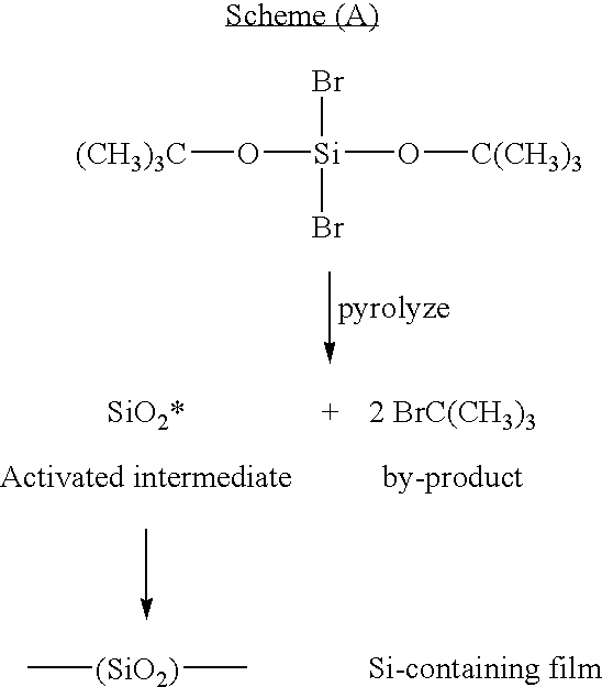
- Other Si precursors of the formula (I) may be used to form Si-containing films in a manner similar to that illustrated in Scheme (A). By-products of such polymerizations preferably comprise R1X1, R1X2, R2X1, and R2X2. Mixtures comprising two or more Si precursors of the formulas (I) and/or (II) may also be used. It will be appreciated that “SiO2*” in Scheme (A) represents various molecular fragments in which the ratio of silicon to oxygen may vary from fragment to fragment, and thus use of “SiO2*” does not imply a particular stoichiometry for all such fragments.
- Examples of Si precursors of the formula (II) include tertiarybutoxy-bromosilane of the formula (V) and tertiarybutoxy-chlorosilane of the formula (VI):

- In another embodiment, deposition using Si precursor (VI) produces a Si-containing film that comprises —(SiH2O)— recurring units and Cl—C(CH3)3 as a by-product as illustrated in Scheme (B):

- Other Si precursors of the formula (II) may be used to form Si-containing films of the general formula —(SiR4R5O)— in a manner similar to that illustrated in Scheme (B). By-products of such polymerizations preferably comprise R3X3. In an embodiment, X3 is fluorine and neither R4 nor R5 are fluorine. Mixtures comprising two or more Si precursors of the formulas (I) and/or (II) may be used to form Si-containing films. For example, in an embodiment, Si-containing films that comprise recurring units of the general formula —[Si(R4R5)O]-[Si(R4′R5′)O]— may be formed from a mixture that comprises two different Si precursors of the formula (II), where the definitions for R4, and R5, are generally the same as those provided above for R4 and R5, respectively, but where R4≠R4′ and/or R5≠R5′ for the two different precursors. In another embodiment, Si-containing films comprising recurring units of the general formula —(SiO2)—(Si(R4R5)O)— may be formed from a mixture that comprises a Si precursors of the formula (I) and a Si precursor of the formula (II). In an embodiment, the Si-containing film is crosslinked. For example, in a Si-containing film that comprises recurring units of the formula —(SiO2)—(Si(R4R5)O)—, the —SiO2— recurring units may form crosslinks. It will be appreciated that “SiH2O*” in Scheme (B) represents various molecular fragments in which the relative ratios of silicon, oxygen and hydrogen may vary from fragment to fragment, and thus use of “SiH2O*” does not imply a particular stoichiometry for all such fragments.
- The temperature for pyrolyzing a Si precursor to form an activated Si-containing intermediate varies, depending on the nature of the Si precursor, and may be identified by routine experimentation in view of the guidance provided herein. Pyrolysis temperatures (e.g., temperatures in the hot zone 235) in the range of about 500° C. to about 850° C., preferably in the range of about 650° to about 750° C., are suitable for a variety of Si precursors of the formulas (I) and (II), although in particular cases higher or lower temperatures may be used. For the embodiment illustrated in
FIG. 2 in which the vaporized Si precursor comprises bis-tertiarybutoxy dibromosilane, theheater 230 preferably heats thereaction chamber 225 to produce a temperature in thehot zone 235 of about 725° C. In some embodiments, e.g., as illustrated in Scheme (A), it may be desirable for the activated Si-containing intermediate to consist essentially of silicon and oxygen. In such embodiments, the pyrolysis temperature is preferably effective to result in the removal of R1, R2, X1 and X2 from Si precursor (I). In other embodiments, e.g., as illustrated in Scheme (B), it may be desirable for the activated Si-containing intermediate to consist essentially of silicon, oxygen, R4 and R5. In such embodiments, the pyrolysis temperature is preferably effective to result in the removal R3 and X3 from Si precursor (II). - Preferably, the pyrolysis temperature (e.g., the temperature in the hot zone 235) facilitates formation of a volatile by-product that does not undesirably contaminate the Si-containing film (e.g., the Si-containing
film 250 that forms on thesubstrate 240 in the cool zone 245). For example, the temperature in thehot zone 235 is preferably lower than the temperature at which reactive by-products (e.g., by-products capable of undesirably reacting with the film 250) are formed. Instead, the pyrolysis conditions are preferably controlled so that any reactive by-products react with one another to form relatively non-reactive volatile by-products, e.g., volatile by-products that do not undergo significant or undesirable chemical reactions with the deposited Si-containing film. - In an embodiment, with reference to the Si precursors of the formulae (I) and (II), X1, X2, X3, R1, R2 and R3 are preferably each individually leaving groups capable of reacting with one or more of each other to form a volatile by-product. Preferably, R3, R4, R5, and X3 are each individually chemical groups selected such that the R4—Si and R5—Si chemical bonds are more stable during the pyrolyzing of the Si precursor than the X3—Si and R3—O bonds. For example, in an embodiment, X1 and X2 are each individually a halogen or H; X3 is a halogen; R1, R2 and R3 are each individually selected from the group consisting of —C(CH3)3, —C6H5, and —NR5R6; and R4, R5 and R6 are each individually selected from the group consisting of hydrogen, deuterium, fluorine, optionally fluorinated C1 to C6 alkyl, optionally fluorinated C1 to C6 cycloalkyl, optionally fluorinated C1 to C6 alkoxy, and optionally fluorinated C6 to C10 aryl. In another embodiment, R1 and R2 are each individually selected from the group consisting of —C(CH3)3 and —CF3, and X1 and X2 are each individually selected from the group consisting of hydrogen, deuterium, fluorine, methyl, and ethyl.
- A Si-containing film may be formed on a substrate by transporting a pyrolyzed Si precursor to a substrate and polymerizing the pyrolyzed Si precursor. Such transport of the pyrolyzed Si precursor is typically from a hot zone (e.g., the hot zone 235) through a transport region downstream of the hot zone to a cool zone (e.g., the cool zone 245) downstream of the transport region. The conditions for transporting the pyrolyzed Si precursor are preferably selected to minimize polymerization of the pyrolyzed Si precursor at the pyrolysis temperature (e.g., in the hot zone 235) or in the gas phase (e.g., during transport through the transport region situated between the
hot zone 235 and the cool zone 245). For example, thesubstrate 240 is preferably maintained at a temperature that is lower than in the transport region between thehot zone 235 and thesubstrate 240. - In an embodiment, transport of the pyrolyzed Si precursor is conducted by use of an inert carrier gas to sweep the pyrolyzed Si precursor from a first zone (e.g., the hot zone 235) to a second zone (e.g., the cool zone 245). This invention is not bound by theory, but it is believed that use of an inert carrier gas tends to dilute the pyrolyzed Si precursor, thereby reducing the rate of gas phase polymerization among activated Si-containing intermediates, and tends to separate activated Si-containing intermediates from other reactive species (such as reactive by-products), thereby reducing the rate of formation of potential Si-containing film contaminants. Use of an inert carrier gas (such as N2, Ar, Xe, and He), instead of a reactive carrier gas, also tends to reduce the formation of species resulting from reaction between the activated Si-containing intermediates and the carrier gas. However, in some embodiments, it is preferable for the carrier gas to contain a minor amount of an oxygen source, e.g., to facilitate production of activated Si-containing intermediates that primarily consist of silicon and oxygen and/or to oxidize the deposited Si-containing film. Examples of suitable oxygen sources include O2, O3, N2O and mixtures thereof.
- After transporting the activated Si-containing intermediate, polymerization to form a Si-containing film typically occurs spontaneously on a substrate that is at a temperature at which polymerization is thermodynamically favorable. The temperature of the substrate (e.g., the substrate 240) is typically selected to facilitate polymerization and is often in the range of about −50° C. to about 300° C., although higher or lower substrate temperatures may be suitable in particular cases. In some embodiments, the substrate is maintained at a relatively low temperature (e.g., in the range of about −25° C. to about 50° C.) to facilitate formation of a Si-containing film that comprises a porogen (discussed in greater detail below) and/or to achieve relatively higher deposition rates. For example, the
substrate 240 may be cooled by thesubstrate holder 242 and thetemperature control unit 243 as discussed above with respect toFIG. 2 . Although cooling may result in the entrapment of by-products (such as Br—C(CH3)3, Scheme (A)) within the Si-containing film and such entrapped by-products may act as porogens, the temperature of the substrate is preferably selected so that the by-products are relatively volatile, so that little if any of the by-products of pyrolysis or polymerization are entrapped within the Si-containing film. Such volatile by-products may be drawn into a cold trap by the vacuum applied to the chamber or may be swept from the deposition chamber by a carrier gas, e.g., as described above with respect toFIG. 2 . In an embodiment, the Si-containing film consists essentially of the polymerization product(s) of the activated Si-containing intermediate(s) formed from the Si precursor(s). In other embodiments, the substrate temperature is selected to be above the boiling temperature of the by-product(s), but below the boiling temperature of the porogen (at the deposition pressure), to facilitate removal of the by-product and incorporation of the porogen. Such embodiments are discussed in greater detail below. - Pyrolysis, transport and polymerization to form a Si-containing film as described above is preferably conducted in a chamber, e.g., the
reaction chamber 225 illustrated inFIG. 2 , although activated Si-containing intermediates may also be transported between separate pyrolysis and polymerization chambers. The pressure in thereaction chamber 225 may be controlled by manipulating the partial pressures of the various constituents (e.g., Si precursor, activated Si-containing intermediate, optional carrier gas, optional oxygen source, and optional porogen), the temperatures in thehot zone 235 and thecool zone 245, and the vacuum applied by thevacuum pump 270. In general, pressures at various stages of the overall process (e.g., during deposition, during subsequent heating, during subsequent porogen removal, see below) may vary over a broad range from about 1×10⁻⁴ Torr to about 7,600 Torr, depending on the nature of the Si precursor and by-product(s), and the structure desired for the resulting Si-containing film (e.g., non-porous, porogen-containing, porous) as described in greater detail below. Deposition rates tend to be a function of pressure (and particularly Si precursor partial pressure), and thus relatively higher deposition rates are typically obtained at relatively higher overall pressures and/or relatively higher Si precursor partial pressures. In certain embodiments, higher Si precursor partial pressures may be achieved at lower overall pressures because such lower pressures may lead to increased volatilization of the Si precursor. - Methods for forming Si-containing films may further comprise various post-deposition film treatments such as annealing and/or oxidizing. The as-deposited Si-containing film may be annealed for various reasons, e.g., to reduce stress, to volatilize porogens and/or by-products, and/or to remove or alter undesirable chemical groups. Porogen removal is discussed in greater detail below. Annealing temperatures are typically in the range of about 50° C. to about 600° C., preferably in the range of about 150° C. to about 450° C. The chamber pressure during annealing is preferably about 600 Torr or less. Annealing times are typically in the range of 10 minutes to about 3 hours, preferably in the range of about 30 minutes to two hours. Annealing may be conducted in the deposition chamber, e.g., without exposing the as-deposited Si-containing film to ambient, and/or may be conducted by annealing an as-deposited or previously treated film after the film is removed from the deposition chamber, e.g., in a separate anneal station. In an embodiment, at least a part of the annealing is conducted under an inert gas (e.g., N2, He, Ar, Ne). In another embodiment, at least a part of the annealing is conducted under a gas selected from the group consisting of nitrogen, helium, hydrogen, a nitrogen/helium mixture, and a nitrogen/hydrogen mixture.
- Oxidation of the Si-containing films may be carried out with or without annealing, and may be carried out for various purposes, e.g., to alter and/or remove undesirable chemical groups from the Si-containing films. For example, in an embodiment in which it is desirable for the Si-containing film to primarily consist essentially of silicon and oxygen, elements such as carbon that may be present in the as-deposited film may be oxidized to form volatile carbon oxides (e.g., CO, CO2) and thereby removed from the film. Oxidation of the Si-containing films may be conducted by exposing the Si-containing film to an oxygen-containing gas (e.g., O2, O3, N2O and mixtures thereof), with or without plasma activation, preferably with annealing, either within the deposition chamber after removing the as-deposited or previously treated film from the deposition chamber.
- Methods for Forming Si-Containing Films that Contain Porogen(s)
- An embodiment provides a method for forming a film that includes transporting a pyrolyzed Si precursor to a substrate and polymerizing the pyrolyzed Si precursor in the presence of a porogen to form a Si-containing film on the substrate, the Si-containing film comprising at least a portion of the porogen. Various suitable methods for making and transporting a pyrolyzed Si precursor to a substrate are discussed above. Polymerization of a pyrolyzed Si precursor in the presence of a porogen to form a porogen-containing Si-containing film is conceptually illustrated in
FIG. 1 as discussed above. Those skilled in the art will appreciate that, in the absence of a porogen or entrapped by-products, polymerization of the pyrolyzed Si precursor typically results in a relatively non-porous film that contains the chemical elements present in the pyrolyzed Si precursor from which it was made. For example, pyrolysis of the Si precursor (III) as illustrated in Scheme (A) produces a pyrolyzed Si precursor represented by SiO2* that consists essentially of silicon and oxygen atoms. Other Si precursors of the formula (I) may be pyrolyzed similarly. Subsequent polymerization of the SiO2* species of Scheme (A) produces a largely inorganic Si-containing film that consists essentially of —(SiO2)— recurring units. In an embodiment, such a Si-containing film is an amorphous, relatively non-porous material that is chemically and structurally similar to silicon dioxide. - Similarly, polymerization of Si precursor (VI) as illustrated in Scheme (B) produces a pyrolyzed Si precursor represented by SiH2O* that primarily consists essentially of silicon, hydrogen and oxygen atoms. Subsequent polymerization of the SiH2O* produces a Si-containing film that primarily consists essentially of —SiH2)— recurring units. In an embodiment, such a Si-containing film is a relatively non-porous material. Other Si precursors of the formula (II) may be pyrolyzed similarly to produce pyrolyzed Si precursors that primarily consist of silicon, oxygen, R4 and R5, and polymerized similarly to form Si-containing films that primarily consist of the same elements as the precursors. In an embodiment, such Si-containing films are also relatively non-porous.
- However, as illustrated conceptually in
FIG. 1 , during polymerization of a pyrolyzed Si precursor represented by SiOx* in the presence of aporogen 110, theporogen 110 becomes entrapped within the polymerization matrix, resulting in the formation of a Si-containingfilm 115 a that comprises at least a portion of theporogen 110 that is present during the polymerization. Theporogen 110 is capable of being removed from the film to form aporous film 115b comprising pores 120 previously occupied by theporogen 110. - As used herein, the term “porogen” refers to a substance or mixture of substances that, when present during the polymerization of a pyrolyzed Si precursor to form a Si-containing film, becomes incorporated into the film in such a way as to permit it to be subsequently removed from the film to produce a porous Si-containing film that has greater porosity than an otherwise comparable Si-containing film formed by formed by an otherwise substantially identical process but in the absence of the porogen. Porogens preferably have a molecular weight of less than about 1,000 Daltons, to facilitate removal from the film. The porogen may be removed from the film during film deposition, and thus it is not necessary to detect a particular substance within a film in order to conclude that it is a porogen. Porogens or portions thereof may become chemically bonded to the film, in which case subsequent removal may involve chemical bond scission. Preferably, at least a portion of the porogen is not chemically bonded to the Si-containing film; more preferably, substantially all of the porogen is not chemically bonded to the Si-containing film.
- Examples of suitable porogens include optionally halogenated C2-C10 alcohol, optionally halogenated C2-C10 diol, optionally halogenated C2-C10 ether, optionally halogenated C2-C10 ketone, optionally halogenated C2-C10 ester, optionally halogenated C2-C10 aldehyde, optionally halogenated C1-C10 hydrocarbon, optionally halogenated C2-C10 carboxylic acid, optionally halogenated C2-C10 anhydride, carbon monoxide, carbon dioxide, and mixtures thereof. Examples of preferred porogens include dimethyl oxalate, di-tertiarybutyl oxalate, carbon tetrabromide, benzene, methanol, t-butanol and mixtures thereof.
-
FIG. 2 illustrates anapparatus 200 suitable for transporting a pyrolyzed Si precursor to a substrate and polymerizing the pyrolyzed Si precursor in the presence of a porogen to form a porogen-containing Si-containing film on the substrate. Theapparatus 200 includes avessel 275 and a feed line 276 running from thevessel 275 to a transport region of thereaction chamber 225 between thehot zone 235 and thecool zone 245. Thevessel 275 contains aporogen 280, which in the illustrated embodiment comprises di-tertiarybutyl oxalate. A bubbler configuration similar to that used to supply theSi precursor 205 to thereaction chamber 225 is used to supply theporogen 280 to thereaction chamber 225. In this configuration, anothervessel 215 a contains a nitrogen carrier gas; other carrier gases such as helium, argon, and/or neon may also be suitable. Afeed line 216 a equipped with avalve 217 a connects thevessel 215 a to thevessel 210. In the illustrated configuration, thevessel 275 is abubbler 218 a by which, during operation, the nitrogen carrier gas supplied by thefeed line 216 a bubbles through theporogen 280 in thestorage vessel 275, thereby vaporizing theporogen 280 to form a vaporized porogen. Afeed line 220 a equipped with avalve 222 a connects thestorage vessel 275 to thereaction chamber 225. It will be understood that the bubbler configuration illustrated inFIG. 2 for the supply of theporogen 280 is optional and may be omitted as desired, e.g., when theporogen 280 has a vapor pressure that is sufficiently high that suitable levels of porogen incorporation into thefilm 250 may be achieved by, e.g., direct draw of theporogen 280 into thereaction chamber 225. In an alternative embodiment (not shown inFIG. 2 ), thestorage vessel 275 is equipped with a heater, and the vaporization of theporogen 280 in thestorage vessel 275 is controlled by manipulating the amount of heat supplied to thestorage vessel 275 by the heater. In an embodiment, the partial pressure of theporogen 280 in thereaction chamber 225 is controlled by manipulating the vacuum applied to thechamber 225 and the temperature of theporogen 280 in thestorage vessel 275, without using a carrier gas. - During operation, the
porogen 280 enters thereaction chamber 225 via thefeed line 220 a and thevalve 222 a. Theporogen 280 flows into thecool zone 245 and into the presence of the pyrolyzed Si precursor at thesubstrate 240. Polymerization of the pyrolyzed Si precursor to form the Si-containingfilm 250 on thesubstrate 240 takes place in the general manner described above, except that at least a portion of theporogen 280 is entrapped within the Si-containingfilm 250 during the polymerization, thereby forming a Si-containing film that comprises a least a portion of theporogen 280. - Methods for forming porogen-containing Si-containing films may further comprise various post-deposition film treatments such as annealing and/or oxidizing. The as-deposited porogen-containing Si-containing film may be annealed for various reasons, e.g., to reduce stress, to remove trapped porogens and/or by-products, and/or to remove or alter undesirable chemical groups. Annealing temperatures are typically in the range of about 50° C. to about 600° C., preferably in the range of about 150° C. to about 450° C. Annealing times are typically in the range of 10 minutes to about 3 hours, preferably in the range of about 30 minutes to two hours. Annealing may be conducted in the deposition chamber, e.g., without exposing the as-deposited porogen-containing Si-containing film to ambient, and/or may be conducted by annealing an as-deposited or previously treated film after the film is removed from the deposition chamber in a separate anneal station, with or without exposure to ambient. For example, annealing may be accomplished by heating the
substrate 240 and the Si-containingfilm 250 using thetemperature control unit 243. The pressure during annealing may be controlled by manipulating the vacuum applied by thevacuum pump 270 viavalve 267. The chamber may also be pressurized by filling thereaction chamber 225 with a gas e.g., by attaching athird gas source 285 to thereaction chamber 225 via avalve 287, using appropriate precautions for dealing with pressurized systems. In an embodiment, at least a part of the annealing is conducted under an inert annealing gas (e.g., N2, He, Ar, Ne). In another embodiment, at least a part of the annealing is conducted under an annealing gas selected from the group consisting of nitrogen, helium, hydrogen, a nitrogen/helium mixture, and a nitrogen/hydrogen mixture. Thus, thethird gas source 285 may comprise such an annealing gas or gases. - Oxidation of the porogen-containing Si-containing films may be carried out with or without annealing, and may be carried out for various purposes, e.g., to alter and/or remove undesirable chemical groups from the Si-containing films and/or to remove the porogen by oxidation. For example, oxidation may be preferred in an embodiment in which removal of the porogen by volatilization is difficult or inconvenient and in which the oxidation of the porogen produces oxides having greater volatility. Oxidation of the Si-containing films and/or porogens contained therein may be conducted by exposing the porogen-containing Si-containing film to an oxygen-containing gas (e.g., O2, O3, N2O and mixtures thereof), with or without plasma activation, preferably with annealing, either within the deposition chamber after removing the as-deposited or previously treated film from the deposition chamber. Such oxygen-containing gases may comprise the
third gas source 285 and thus may be introduced into thereaction chamber 225 via thevalve 287. - As noted above, the chamber pressure may be varied over a broad range, e.g., from about 7,600 Torr to about 1×10⁻⁴ Torr, depending on the stage of the overall process. In one embodiment, the pressure during annealing is relatively low to facilitate removal of the porogen, as discussed in greater detail below. In another embodiment, the pressure during annealing or during an annealing stage is relatively high, e.g. in the range of about 760 Torr to about 7,600 Torr. Such pressures may be applied during annealing to minimize or prevent volatilization of an entrapped porogen from a Si-containing film during annealing. For example, prior to removing the porogen, it may be desirable to anneal a porogen-containing Si-containing film to stabilize the structure of the Si-containing film surrounding the porogen.
- Porogen-containing Si-containing films (e.g., the
film 115 a inFIG. 1 ) preferably contain an amount of porogen that is effective to produce a porous film (e.g., thefilm 115 b inFIG. 1 ) having the desired degree of porosity upon removal of the porogen. Amounts of porogen in the porogen-containing Si-containing film may vary over a broad range, e.g., form about 0.001% to about 70% by weight, based on total film weight, depending on the application. The dielectric constants of porous films generally decrease as the degree of porosity increases, but in many cases the mechanical properties of porous films also tend to decrease as the degree of porosity increases. Thus, preferred levels of porogen in a particular porogen-containing Si-containing film typically represent a balance between dielectric and mechanical properties, and may be in the range of about 0.01% to about 40%, more preferably about 1% to about 30%, by weight based on total film weight. The porogen may be distributed relatively uniformly throughout the film or varied as a function of position within the film. - In an embodiment, the amount of porogen in the porogen-containing Si-containing film is varied as a function of depth in the film. For example, in certain embodiments it may be desirable to form a graded porous Si-containing film having a degree of porosity that changes as a function of depth in the film. One way of making such a graded film is from a similarly graded porogen-containing Si-containing film. The amount of porogen incorporated into the porogen-containing Si-containing at any particular film depth is a function of the relative amount of porogen present during the polymerization of the pyrolyzed Si precursor. The relative amount of porogen may be controlled in various ways. For example, in the illustrated embodiment, the
valve 222 a and/or the flow of thenitrogen carrier gas 215 a (via thevalve 217 a) may be manipulated during deposition to control the flow of theporogen 280 into thereaction chamber 225. The relative amount of porogen present during polymerization may also be controlled by varying the amount of Si precursor, e.g., by reducing the flow of the Si precursor 215 (e.g., by manipulation of thevalve 217 and/or the valve 222), thereby increasing the relative amount of theporogen 280 at thesubstrate 240, or vice-versa. Mass flow controllers (MFC's) may be provided in addition to or in place of each of the indicated valves inFIG. 2 . In an embodiment, the concentration of porogen in the film is graded, e.g., the concentration of porogen is lower near a surface of a porogen-containing Si-containing film as compared to the concentration of porogen near the center of the porogen-containing Si-containing film. Such a graded concentration porogen-containing Si-containing film is useful for making correspondingly graded porous films by removal of the porogen as discussed below. - Methods for Forming Porous Films
- An embodiment provides a method for forming a porous film, comprising: transporting a pyrolyzed Si precursor to a substrate; polymerizing the pyrolyzed Si precursor in the presence of a porogen to form a Si-containing polymer; and forming a porous Si-containing film on the substrate, the porous Si-containing film comprising the Si-containing polymer. Various suitable methods for making a pyrolyzed Si precursor, transporting it to a substrate, and polymerizing it in the presence of a porogen are discussed above. In some embodiments, such polymerization results in the formation of a porous Si-containing film, without the formation of a discrete intermediate porogen-containing Si-containing film. In other embodiments, e.g., as illustrated conceptually in
FIG. 1 , the method involves forming a porogen-containingintermediate film 115 a and then removing theporogen 110 to create the porous Si-containingfilm 115 b. Preferably, in such embodiments, the method further comprises depositing the Si-containing polymer and the porogen on the substrate to thereby form the porogen-containing Si-containingfilm 115 a on thesubstrate 105; and removing at least a portion of theporogen 110 from the porogen-containing Si-containingfilm 115 a to thereby form the porous Si-containingfilm 115 b. - Porogens may be removed in various ways from porogen-containing Si-containing films to form porous Si-containing films. It has been found that a number of factors may affect porogen removal including porogen volatility, time, temperature, pressure, and/or environmental conditions (e.g., presence or absence of water, oxygen, hydrogen, inert gas, etc., during porogen removal). In most cases, removal of the porogen may be accomplished by establishing suitable volatilization conditions, e.g., by manipulating the temperature and pressure applied to the porogen-containing Si-containing film so that the film is at a temperature that is near or above the boiling point or sublimation temperature of the porogen at the applied pressure. The volatilization conditions (e.g., temperature and pressure) for a particular porogen may be readily determined by consulting the appropriate literature references known to those skilled in the art or by routine experimentation. Temperatures lower than the boiling or sublimation point of the particular porogen at the applied pressure may be suitable, but result in slower volatilization. Those skilled in the art will appreciate that relatively faster and more complete volatilization is typically achieved by applying relatively higher temperatures and/or lower pressures.
- The porous Si-containing film may be formed in the same chamber as the porogen-containing Si-containing film. For example, as discussed above with reference to
FIG. 2 , the as-deposited Si-containingfilm 250 may be heated for various reasons, e.g., to reduce stress, to volatilize porogens and/or by-products, and/or to remove or alter undesirable chemical groups. In an embodiment in which the Si-containingfilm 250 comprises aporogen 280, theporogen 280 may be removed while the Si-containingfilm 250 remains in thereaction chamber 225. For example, porogen removal may be accomplished by heating thesubstrate 240 and the Si-containingfilm 250 using thetemperature control unit 243. Manipulating the vacuum applied by thevacuum pump 270 viavalve 267 may control the pressure during removal. The chamber may also be pressurized by filling thereaction chamber 225 with a gas (e.g., thenitrogen gas third gas 285 may be selected from the group consisting of N2, He, Ar, Ne, hydrogen, and mixtures thereof such as nitrogen/helium and nitrogen/hydrogen. In addition to or instead of conducting porogen removal in thereaction chamber 225, porogen removal may be accomplished after removing the Si-containingfilm 250 from thereaction chamber 225, e.g., by allowing porogen volatilization under ambient conditions and/or by placing the Si-containingfilm 250 into a second chamber (not shown), with or without exposure to ambient, and applying the appropriate temperature/pressure/time conditions. Temperatures during porogen removal are typically in the range of about 50° C. to about 600° C., preferably in the range of about 150° C. to about 450° C. Porogen removal times are typically in the range of 10 minutes to about 3 hours, preferably in the range of about 30 minutes to two hours. Pressure during porogen removal may be in the range of about 7,600 Torr to about 1×10⁻⁴ Torr, preferably about 600 Torr or less, more preferably about 50 Torr or less, even more preferably about 1 Torr or less. - Removal of the porogen from the porogen-containing Si-containing film may also be accomplished by chemically reacting the porogen (e.g., by exposing the porogen-containing Si-containing film to a reactive gas), thereby forming porogen by-products that may then be removed from the film. For example, the
third gas 285 may comprise an oxygen-containing gas (e.g., O2, O3, N2O and mixtures thereof) or a gas that comprises hydrogen such as hydrogen itself or a nitrogen/hydrogen mixture. Thethird gas 285 may be introduced to thereaction chamber 225 during all or a portion of the time that the porogen is being removed from the porogen-containing film, thereby reacting with the porogen to form volatile by-products. Temperatures during such reactive removal of the porogen are typically in the range of about 50° C. to about 600° C., preferably in the range of about 150° C. to about 450° C. The porogen-containing Si-containing film may be exposed to the reactive gas for periods of time in the range of 10 minutes to about 3 hours, preferably in the range of about 30 minutes to two hours. Pressure during reactive removal may be in the range of about 7,600 Torr to about 1×10⁻⁴ Torr, preferably about 600 Torr or less, more preferably about 50 Torr or less, even more preferably about 1 Torr or less. Reactive removal is preferred when the porogen is chemically bonded to the porogen-containing Si-containing film. - The porosity of the porous Si-containing film (e.g., the
film 115 b) may be varied over a broad range by controlling the amount of theporogen 110 incorporated into the porogen-containingfilm 115 a and by controlling the amount ofporogen 110 removed from the porogen-containingfilm 115 a during porogen removal. As discussed above, the porogen-containing Si-containingfilms 115 a preferably contain an amount of porogen that is effective to produce aporous film 115 b having the desired degree of porosity upon removal of the porogen. In an embodiment, porous Si-containing films are suitable for use as low-k films in semiconductor and MEMS applications. The dielectric constants of porous films generally decrease as the degree of porosity increases, but in many cases the mechanical properties of porous films also tend to decrease as the degree of porosity increases. Thus, depending on the balance of mechanical and dielectric properties desired for a particular application, the dielectric constant of the porous Si-containing film may vary over a broad range from about 1.8 to about 4.0, preferably from about 2.0 to about 3.8. - It will be appreciated that the methods described herein may be used to incorporate the porogen into the porogen-containing film in highly uniform manner that minimizes undesirable levels of clustering or agglomeration of the porogen within film. For example, the porogen may be finely dispersed within the porogen containing film at the molecular level. Such uniformity may be maintained upon removal, such that a substantial fraction of the pores in the resulting porous Si-containing film have a size that corresponds to size of the porogen molecule that previously occupied the pore. Thus, in an embodiment, the porous Si-containing film comprises nanopores. Preferred porous Si-containing films comprise nanopores having a size that corresponds to about 10 porogen molecules or less, more preferably about 5 porogen molecules or less, even more preferably about 2 porogen molecules or less. Depending on the size of the porogen molecule(s) used to form the porous film, the number average volume of the pores in the Si-containing film may be about 10 nm3 or less, preferably about 5 nm3 or less, even more preferably about one nm3 or less. Porosity may be characterized by atomic force microscopy of cross-sectioned samples. The density of the porous Si-containing films may also vary over a broad range, depending on the degree of porosity. In an embodiment, porous Si-containing films have a density of about 2.34 g/cm−3 or less, preferably about 2.08 g/cm−3 or less, more preferably about 1.82 g/cm−3 or less, even more preferably about 1.56 g/cm−3 or less.
- In an embodiment, the porous Si-containing film has a degree of porosity that changes as a function of depth in the film. Such a film may be prepared by volatilizing the porogen from a porogen-containing Si-containing film in which the amount of porogen is varied as a function of depth in the film. Methods for making such graded porogen-containing films are described above. The general methods described above for volatilizing the porogen from porogen-containing films also apply to graded porogen-containing films. In an embodiment, the degree of porosity is lower near a surface of a porous Si-containing film as compared to the degree of porosity near the center of the porous Si-containing film. Such porous Si-containing films may have a graded mechanical property profile in which the mechanical properties are higher near the surface (where porosity is lower). In some cases, uniform porous materials may have correspondingly weaker mechanical properties, and thus may have undesirably weaker surface interactions (such as bond strengths) with other materials. In an embodiment, graded porous Si-containing films (having a degree of porosity that is lower near a surface than near the center) have relatively low dielectric constants (e.g., in the range of about 3.3 to about 3.8) and acceptable surface interactions (such as bond strength) with other materials, comparable to or only slightly less (e.g., less than 10% reduction) than bulk SiO2.
- As discussed above,
FIG. 1 conceptually illustrates forming theporous film 115 b that containspores 120 previously occupied by theporogen 110. The illustrated embodiment involves the formation of an intermediate porogen-containing Si-containingfilm 115 a that comprises at least a portion of theporogen 110 that is present during the polymerization of SiOx*. However, it will be appreciated that theporogen 110 may be trapped within thefilm 115 a for relatively short periods of time, e.g., for a time that is less than the formation time for theporous film 115 b, and/or the presence of the porogen may initiate the formation of pores in the resultingfilm 115 b without the porogen becoming trapped in thefilm 115 a, and/or the structure and porogen content of thefilm 115 a may change during deposition. Thus, in some embodiments the intermediate porogen-containingfilm 115 a is difficult to characterize, short-lived, transient or variable in nature. In other embodiments, theporous film 115 b is formed directly from the polymerization of SiOx* in the presence of theporogen 110, without the formation of the discrete intermediate porogen-containing Si-containingfilm 115 a per se. Thus, methods described herein for making porous films from intermediate porogen-containing film also apply to porous films formed directly from the polymerization of SiOx* in the presence of the porogen. - Depositions described in the Examples below were carried out using a deposition system of the general design illustrated in
FIG. 2 . The system was cleaned and thoroughly dried using heating and pumping overnight under vacuum (diffusion pump,nominal vacuum 10−5 Torr) using a cold trap (liquid nitrogen, about −196° C.) prior to deposition. During deposition, the precursor was fed by unimpeded direct vapor draw at the nominal pressure applied by the diffusion pump, the temperature in the hot zone was about 725° C., and the cold trap was maintained at about −196° C., unless otherwise stated. Si-precursor, porogen, substrate temperature, and annealing conditions were varied as described below. - Two Si-containing films were deposited using bis-tertiarybutoxy dichlorosilane of the formula (IV). No porogen was used. The substrate temperature was about 0° C. By-product Cl—C(CH3)3 was isolated from the cold trap, indicating that SiOx* was formed and subsequently polymerized to form the Si-containing film (comprising —(SiO2)— recurring units) in a manner similar to that illustrated in Scheme (A) for bis-tertiarybutoxy dibromosilane. After deposition, both films were exposed to air for several days. The films were then thermally annealed at 420° C. for one hour under either air (Example 1) or nitrogen (Example 2). The resulting Si-containing films were characterized by infrared spectroscopy (FTIR) as shown in
FIG. 3 . The FTIR spectra shown inFIG. 3 confirm that the deposited film was a three-dimensional network of silicon and oxygen atoms comprising —(SiO2)— recurring units. - A Si-containing film was deposited using bis-tertiarybutoxy dibromosilane of the formula (III). No porogen was used. The substrate temperature was about 0° C. By-product Br—C(CH3)3 was isolated from the cold trap, indicating that SiOx* was formed and subsequently polymerized to form the Si-containing film (comprising —(SiO2)— recurring units as illustrated in Scheme (A)). The resulting Si-containing film was characterized by FTIR before annealing (Example 3) and after annealing at 400° C. for one hour under vacuum (Example 4) as shown in
FIG. 4 . The FTIR spectra shown inFIG. 4 confirm that both of the films were three-dimensional networks of silicon and oxygen atoms comprising —(SiO2)— recurring units. The spectra also show that the as-deposited film (Example 3) contained Si—OH bonds after exposure to air as indicated by the Si—OH stretching-bending mode observed near 925 cm−1, and that annealing under vacuum (Example 4) changed the structure of the film by reducing the amount of hydroxyl groups in the network. - A Si-containing film was deposited in the same manner described for Examples 3-4 and characterized by FTIR before annealing (Example 5) and after annealing at 400° C. for one hour under a gas mixture containing 5% H2 and 95% N2 (Example 6) as shown in
FIG. 5 . The FTIR spectra shown inFIG. 5 confirm that both of the films were three-dimensional networks of silicon and oxygen atoms comprising —(SiO2)— recurring units. The spectra also show that the as-deposited film (Example 5) contained Si—OH bonds after exposure to air as indicated by the Si—OH stretching-bending mode observed near 925 cm−1, and that annealing under H2/N2 (Example 6) changed the structure of the film by reducing the amount of hydroxyl groups in the network. - A Si-containing film was deposited using tertiarybutoxy chlorosilane of the formula (VI). No porogen was used. The substrate temperature was about 20° C. By-product Cl—C(CH3)3 was isolated from the cold trap, indicating that SiH2O* was formed and subsequently polymerized to form the Si-containing film (comprising —(SiH2O)— recurring units) in the manner illustrated in Scheme (B). The Si-containing film was characterized by FTIR as shown in
FIG. 6 . The FTIR spectrum shown inFIG. 6 exhibits strong Si—H stretching at ˜2189 cm−1, strong Si—O stretching at ˜1106 cm−1, strong Si—H bending at 850 cm−1, and strong Si—O bending at ˜716 cm−1. The FTIR spectrum confirms that the deposited film comprised —SiH2O)— recurring units. The lack of Si—O rocking peaks in the spectrum indicates that the film did not have a three-dimensional SiO2 structure. - A Si-containing film was deposited using bis-tertiarybutoxy silane of the formula H2Si(OC(CH3)3)2 at a hot zone temperature of about 650° C. No porogen was used. The substrate temperature was about 20° C. The Si-containing film was characterized by FTIR as shown in
FIG. 7 . The FTIR spectrum shown inFIG. 7 is very similar to that ofFIG. 6 , indicating that the deposited film comprised —SiH2O)— recurring units and lacked a three-dimensional SiO2 structure. - A Si-containing film was deposited using a mixture of bis-tertiarybutoxy dibromosilane of the formula (III) and bis-tertiarybutoxy silane of the formula H2Si(OC(CH3)3)2 at a hot zone temperature of about 700° C. No porogen was used. The substrate temperature was about 0° C. The Si-containing film was characterized by FTIR as shown in
FIG. 8 . The FTIR spectrum shown inFIG. 8 confirms that the film comprises both —(SiO2)— and —(SiH2O)— recurring units (compare toFIG. 4 andFIG. 7 ). - A series of Si-containing films were deposited in the manner described in Example 9, except that each of the films was deposited using a different ratio for the partial pressure of bis-tertiarybutoxy dibromosilane to bis-tertiarybutoxy silane to thereby control the ratio of —(SiO2)— to —(SiH2O)— recurring units, respectively, incorporated into the film. The Si-containing film of Example 10 was deposited using bis-tertiarybutoxy dibromosilane (without bis-tertiarybutoxy silane); the Si-containing film of Example 14 was deposited using bis-tertiarybutoxy silane (without bis-tertiarybutoxy dibromosilane); and the Si-containing films of Examples 11-13 were deposited using both Si-precursors, at various intermediate ratios. The resulting Si-containing films were characterized by FTIR as shown in
FIG. 9 . The FTIR spectra shown inFIG. 9 demonstrate that the compositions of the films varied in accordance with the partial pressures of the Si precursors. - A Si-containing film was deposited using bis-tertiarybutoxy dibromosilane of the formula (III). The substrate temperature was about 0° C. By-product Br—C(CH3)3 was isolated from the cold trap, indicating that SiOx* was formed and subsequently polymerized to form the Si-containing film (comprising —(SiO2)— recurring units as illustrated in Scheme (A)). A dimethyl oxalate porogen was introduced to the chamber and was present at the substrate during the polymerization of the SiOx*. The resulting porogen-containing Si-containing film was characterized by FTIR soon after deposition (Example 15) and after exposure to air at room temperature for several days (Example 16) as shown in
FIG. 10 . The FTIR spectra shown inFIG. 10 confirm that both of the films were three-dimensional networks of silicon and oxygen atoms comprising —(SiO2)— recurring units. The FTIR spectra also confirm that the as-deposited film (Example 15) contained the dimethyl oxalate porogen (as indicated by carbonyl bands at about ˜1700 cm−1) and that the dimethyl oxalate porogen was removed by exposure to air at room temperature for several days (Example 16). Characterization of the air-exposed film (Example 16) by scanning electron microscopy (SEM) as illustrated inFIG. 11 revealed morphology changes consistent with the formation of porosity in the Si-containing film by the removal of the porogen. - A Si-containing film was deposited using bis-tertiarybutoxy dibromosilane of the formula (III). The substrate temperature was about 0° C. By-product Br—C(CH3)3 was isolated from the cold trap, indicating that SiOx* was formed and subsequently polymerized to form the Si-containing film (comprising —(SiO2)— recurring units as illustrated in Scheme (A). A di-tertiarybutyl oxalate porogen was introduced to the chamber and was present at the substrate during the polymerization of the SiOx*. The resulting porogen-containing Si-containing film was characterized by FTIR before annealing (Example 17,
FIG. 12 ), after several days exposure to air at room temperature (Example 18,FIG. 13 ), and after annealing at 425° C. for one hour in air (Example 19,FIG. 14 ). The FTIR spectra shown inFIGS. 12-14 confirm that all three of the films were three-dimensional networks of silicon and oxygen atoms comprising —(SiO2)— recurring units. The FTIR spectra shown inFIGS. 12-13 also confirm that the as-deposited film (Example 17,FIG. 12 ) contained the di-tertiarybutyl oxalate porogen (as indicated by carbonyl bands at about ˜1700 cm−1) and that at least a portion of the di-tertiarybutyl oxalate porogen remained in the film after several days exposure to air at room temperature (Example 18,FIG. 13 ). The FTIR spectrum shown inFIG. 14 confirms that the porogen was removed by annealing the porogen-containing film at 425° C. for one hour in air. Characterization of the annealed film (Example 19) by SEM reveals morphology changes consistent with the formation of porosity in the Si-containing film by the removal of the porogen. - A Si-containing film was deposited using a mixture of bis-tertiarybutoxy dibromosilane of the formula (III) and tertiarybutoxy-dimethylchlorosilane of the formula Cl(CH3)2SiOC(CH3)3. No porogen was used. The substrate temperature was about 0° C. The as-deposited Si-containing film (Example 20) was characterized by FTIR as shown in
FIG. 14 . The FTIR spectrum shown inFIG. 14 confirms that the film comprised both —(SiO2)— and —(CH3)2SiO)— recurring units. The as-deposited Si-containing film was annealed in air at 450° C. for one hour (Example 21) and characterized by FTIR as shown inFIG. 15 . The FTIR spectrum shown inFIG. 15 confirms that annealing changed the structure of the as-deposited film by reducing the amount of hydroxyl groups. - All patents, patent applications and papers mentioned herein are hereby incorporated by reference in their entireties. It will be appreciated by those skilled in the art that various omissions, additions and modifications may be made to the processes described above without departing from the scope of the invention, and all such modifications and changes are intended to fall within the scope of the invention, as defined by the appended claims.
Claims (81)


Priority Applications (1)
| Application Number | Priority Date | Filing Date | Title |
|---|---|---|---|
| US11/117,988 US7425350B2 (en) | 2005-04-29 | 2005-04-29 | Apparatus, precursors and deposition methods for silicon-containing materials |
Applications Claiming Priority (1)
| Application Number | Priority Date | Filing Date | Title |
|---|---|---|---|
| US11/117,988 US7425350B2 (en) | 2005-04-29 | 2005-04-29 | Apparatus, precursors and deposition methods for silicon-containing materials |
Publications (2)
| Publication Number | Publication Date |
|---|---|
| US20060247404A1 true US20060247404A1 (en) | 2006-11-02 |
| US7425350B2 US7425350B2 (en) | 2008-09-16 |
Family
ID=37235324
Family Applications (1)
| Application Number | Title | Priority Date | Filing Date |
|---|---|---|---|
| US11/117,988 Active 2026-04-02 US7425350B2 (en) | 2005-04-29 | 2005-04-29 | Apparatus, precursors and deposition methods for silicon-containing materials |
Country Status (1)
| Country | Link |
|---|---|
| US (1) | US7425350B2 (en) |
Cited By (247)
| Publication number | Priority date | Publication date | Assignee | Title |
|---|---|---|---|---|
| US20080223455A1 (en) * | 2007-03-16 | 2008-09-18 | Ckd Corporation | Gas supply unit |
| US20110215445A1 (en) * | 2010-02-04 | 2011-09-08 | Air Products And Chemicals, Inc. | Methods to Prepare Silicon-Containing Films |
| US20170207083A1 (en) * | 2016-01-19 | 2017-07-20 | Samsung Electronics Co., Ltd. | Methods of forming a low-k dielectric layer and methods of fabricating a semiconductor device using the same |
| JP2019507750A (en) * | 2016-02-12 | 2019-03-22 | シースター ケミカルズ ユーエルシー | Organometallic compounds and methods |
| US10279959B2 (en) | 2012-12-11 | 2019-05-07 | Versum Materials Us, Llc | Alkoxysilylamine compounds and applications thereof |
| US10685834B2 (en) | 2017-07-05 | 2020-06-16 | Asm Ip Holdings B.V. | Methods for forming a silicon germanium tin layer and related semiconductor device structures |
| US10714350B2 (en) | 2016-11-01 | 2020-07-14 | ASM IP Holdings, B.V. | Methods for forming a transition metal niobium nitride film on a substrate by atomic layer deposition and related semiconductor device structures |
| US10714385B2 (en) | 2016-07-19 | 2020-07-14 | Asm Ip Holding B.V. | Selective deposition of tungsten |
| US10714335B2 (en) | 2017-04-25 | 2020-07-14 | Asm Ip Holding B.V. | Method of depositing thin film and method of manufacturing semiconductor device |
| US10720331B2 (en) | 2016-11-01 | 2020-07-21 | ASM IP Holdings, B.V. | Methods for forming a transition metal nitride film on a substrate by atomic layer deposition and related semiconductor device structures |
| US10734497B2 (en) | 2017-07-18 | 2020-08-04 | Asm Ip Holding B.V. | Methods for forming a semiconductor device structure and related semiconductor device structures |
| US10734223B2 (en) | 2017-10-10 | 2020-08-04 | Asm Ip Holding B.V. | Method for depositing a metal chalcogenide on a substrate by cyclical deposition |
| US10731249B2 (en) | 2018-02-15 | 2020-08-04 | Asm Ip Holding B.V. | Method of forming a transition metal containing film on a substrate by a cyclical deposition process, a method for supplying a transition metal halide compound to a reaction chamber, and related vapor deposition apparatus |
| US10741385B2 (en) | 2016-07-28 | 2020-08-11 | Asm Ip Holding B.V. | Method and apparatus for filling a gap |
| US10755922B2 (en) | 2018-07-03 | 2020-08-25 | Asm Ip Holding B.V. | Method for depositing silicon-free carbon-containing film as gap-fill layer by pulse plasma-assisted deposition |
| US10767789B2 (en) | 2018-07-16 | 2020-09-08 | Asm Ip Holding B.V. | Diaphragm valves, valve components, and methods for forming valve components |
| US10770336B2 (en) | 2017-08-08 | 2020-09-08 | Asm Ip Holding B.V. | Substrate lift mechanism and reactor including same |
| US10784102B2 (en) | 2016-12-22 | 2020-09-22 | Asm Ip Holding B.V. | Method of forming a structure on a substrate |
| US10787741B2 (en) | 2014-08-21 | 2020-09-29 | Asm Ip Holding B.V. | Method and system for in situ formation of gas-phase compounds |
| US10797133B2 (en) | 2018-06-21 | 2020-10-06 | Asm Ip Holding B.V. | Method for depositing a phosphorus doped silicon arsenide film and related semiconductor device structures |
| US10804098B2 (en) | 2009-08-14 | 2020-10-13 | Asm Ip Holding B.V. | Systems and methods for thin-film deposition of metal oxides using excited nitrogen-oxygen species |
| US10811256B2 (en) | 2018-10-16 | 2020-10-20 | Asm Ip Holding B.V. | Method for etching a carbon-containing feature |
| US10818758B2 (en) | 2018-11-16 | 2020-10-27 | Asm Ip Holding B.V. | Methods for forming a metal silicate film on a substrate in a reaction chamber and related semiconductor device structures |
| US10832903B2 (en) | 2011-10-28 | 2020-11-10 | Asm Ip Holding B.V. | Process feed management for semiconductor substrate processing |
| US10829852B2 (en) | 2018-08-16 | 2020-11-10 | Asm Ip Holding B.V. | Gas distribution device for a wafer processing apparatus |
| US10847366B2 (en) | 2018-11-16 | 2020-11-24 | Asm Ip Holding B.V. | Methods for depositing a transition metal chalcogenide film on a substrate by a cyclical deposition process |
| US10847371B2 (en) | 2018-03-27 | 2020-11-24 | Asm Ip Holding B.V. | Method of forming an electrode on a substrate and a semiconductor device structure including an electrode |
| US10844486B2 (en) | 2009-04-06 | 2020-11-24 | Asm Ip Holding B.V. | Semiconductor processing reactor and components thereof |
| US10844484B2 (en) | 2017-09-22 | 2020-11-24 | Asm Ip Holding B.V. | Apparatus for dispensing a vapor phase reactant to a reaction chamber and related methods |
| US10847365B2 (en) | 2018-10-11 | 2020-11-24 | Asm Ip Holding B.V. | Method of forming conformal silicon carbide film by cyclic CVD |
| US10851456B2 (en) | 2016-04-21 | 2020-12-01 | Asm Ip Holding B.V. | Deposition of metal borides |
| US10858737B2 (en) | 2014-07-28 | 2020-12-08 | Asm Ip Holding B.V. | Showerhead assembly and components thereof |
| US10865475B2 (en) | 2016-04-21 | 2020-12-15 | Asm Ip Holding B.V. | Deposition of metal borides and silicides |
| US10867786B2 (en) | 2018-03-30 | 2020-12-15 | Asm Ip Holding B.V. | Substrate processing method |
| US10867788B2 (en) | 2016-12-28 | 2020-12-15 | Asm Ip Holding B.V. | Method of forming a structure on a substrate |
| US10872771B2 (en) | 2018-01-16 | 2020-12-22 | Asm Ip Holding B. V. | Method for depositing a material film on a substrate within a reaction chamber by a cyclical deposition process and related device structures |
| US10886123B2 (en) | 2017-06-02 | 2021-01-05 | Asm Ip Holding B.V. | Methods for forming low temperature semiconductor layers and related semiconductor device structures |
| US10883175B2 (en) | 2018-08-09 | 2021-01-05 | Asm Ip Holding B.V. | Vertical furnace for processing substrates and a liner for use therein |
| US10892156B2 (en) | 2017-05-08 | 2021-01-12 | Asm Ip Holding B.V. | Methods for forming a silicon nitride film on a substrate and related semiconductor device structures |
| US10896820B2 (en) | 2018-02-14 | 2021-01-19 | Asm Ip Holding B.V. | Method for depositing a ruthenium-containing film on a substrate by a cyclical deposition process |
| US10910262B2 (en) | 2017-11-16 | 2021-02-02 | Asm Ip Holding B.V. | Method of selectively depositing a capping layer structure on a semiconductor device structure |
| US10914004B2 (en) | 2018-06-29 | 2021-02-09 | Asm Ip Holding B.V. | Thin-film deposition method and manufacturing method of semiconductor device |
| US10923344B2 (en) | 2017-10-30 | 2021-02-16 | Asm Ip Holding B.V. | Methods for forming a semiconductor structure and related semiconductor structures |
| US10928731B2 (en) | 2017-09-21 | 2021-02-23 | Asm Ip Holding B.V. | Method of sequential infiltration synthesis treatment of infiltrateable material and structures and devices formed using same |
| US10934619B2 (en) | 2016-11-15 | 2021-03-02 | Asm Ip Holding B.V. | Gas supply unit and substrate processing apparatus including the gas supply unit |
| US10941490B2 (en) | 2014-10-07 | 2021-03-09 | Asm Ip Holding B.V. | Multiple temperature range susceptor, assembly, reactor and system including the susceptor, and methods of using the same |
| US10943771B2 (en) | 2016-10-26 | 2021-03-09 | Asm Ip Holding B.V. | Methods for thermally calibrating reaction chambers |
| USD913980S1 (en) | 2018-02-01 | 2021-03-23 | Asm Ip Holding B.V. | Gas supply plate for semiconductor manufacturing apparatus |
| US10975470B2 (en) | 2018-02-23 | 2021-04-13 | Asm Ip Holding B.V. | Apparatus for detecting or monitoring for a chemical precursor in a high temperature environment |
| US11001925B2 (en) | 2016-12-19 | 2021-05-11 | Asm Ip Holding B.V. | Substrate processing apparatus |
| US11004977B2 (en) | 2017-07-19 | 2021-05-11 | Asm Ip Holding B.V. | Method for depositing a group IV semiconductor and related semiconductor device structures |
| US11018047B2 (en) | 2018-01-25 | 2021-05-25 | Asm Ip Holding B.V. | Hybrid lift pin |
| US11018002B2 (en) | 2017-07-19 | 2021-05-25 | Asm Ip Holding B.V. | Method for selectively depositing a Group IV semiconductor and related semiconductor device structures |
| US11015245B2 (en) | 2014-03-19 | 2021-05-25 | Asm Ip Holding B.V. | Gas-phase reactor and system having exhaust plenum and components thereof |
| US11022879B2 (en) | 2017-11-24 | 2021-06-01 | Asm Ip Holding B.V. | Method of forming an enhanced unexposed photoresist layer |
| US11024523B2 (en) | 2018-09-11 | 2021-06-01 | Asm Ip Holding B.V. | Substrate processing apparatus and method |
| US11031242B2 (en) | 2018-11-07 | 2021-06-08 | Asm Ip Holding B.V. | Methods for depositing a boron doped silicon germanium film |
| USD922229S1 (en) | 2019-06-05 | 2021-06-15 | Asm Ip Holding B.V. | Device for controlling a temperature of a gas supply unit |
| US11049751B2 (en) | 2018-09-14 | 2021-06-29 | Asm Ip Holding B.V. | Cassette supply system to store and handle cassettes and processing apparatus equipped therewith |
| US11053591B2 (en) | 2018-08-06 | 2021-07-06 | Asm Ip Holding B.V. | Multi-port gas injection system and reactor system including same |
| US11056344B2 (en) | 2017-08-30 | 2021-07-06 | Asm Ip Holding B.V. | Layer forming method |
| US11056567B2 (en) | 2018-05-11 | 2021-07-06 | Asm Ip Holding B.V. | Method of forming a doped metal carbide film on a substrate and related semiconductor device structures |
| US11069510B2 (en) | 2017-08-30 | 2021-07-20 | Asm Ip Holding B.V. | Substrate processing apparatus |
| US11081345B2 (en) | 2018-02-06 | 2021-08-03 | Asm Ip Holding B.V. | Method of post-deposition treatment for silicon oxide film |
| US11087997B2 (en) | 2018-10-31 | 2021-08-10 | Asm Ip Holding B.V. | Substrate processing apparatus for processing substrates |
| US11088002B2 (en) | 2018-03-29 | 2021-08-10 | Asm Ip Holding B.V. | Substrate rack and a substrate processing system and method |
| US11094582B2 (en) | 2016-07-08 | 2021-08-17 | Asm Ip Holding B.V. | Selective deposition method to form air gaps |
| US11094546B2 (en) | 2017-10-05 | 2021-08-17 | Asm Ip Holding B.V. | Method for selectively depositing a metallic film on a substrate |
| US11101370B2 (en) | 2016-05-02 | 2021-08-24 | Asm Ip Holding B.V. | Method of forming a germanium oxynitride film |
| US11114294B2 (en) | 2019-03-08 | 2021-09-07 | Asm Ip Holding B.V. | Structure including SiOC layer and method of forming same |
| US11114283B2 (en) | 2018-03-16 | 2021-09-07 | Asm Ip Holding B.V. | Reactor, system including the reactor, and methods of manufacturing and using same |
| USD930782S1 (en) | 2019-08-22 | 2021-09-14 | Asm Ip Holding B.V. | Gas distributor |
| US11127589B2 (en) | 2019-02-01 | 2021-09-21 | Asm Ip Holding B.V. | Method of topology-selective film formation of silicon oxide |
| US11127617B2 (en) | 2017-11-27 | 2021-09-21 | Asm Ip Holding B.V. | Storage device for storing wafer cassettes for use with a batch furnace |
| USD931978S1 (en) | 2019-06-27 | 2021-09-28 | Asm Ip Holding B.V. | Showerhead vacuum transport |
| US11139191B2 (en) | 2017-08-09 | 2021-10-05 | Asm Ip Holding B.V. | Storage apparatus for storing cassettes for substrates and processing apparatus equipped therewith |
| US11139308B2 (en) | 2015-12-29 | 2021-10-05 | Asm Ip Holding B.V. | Atomic layer deposition of III-V compounds to form V-NAND devices |
| US11158513B2 (en) | 2018-12-13 | 2021-10-26 | Asm Ip Holding B.V. | Methods for forming a rhenium-containing film on a substrate by a cyclical deposition process and related semiconductor device structures |
| US11171025B2 (en) | 2019-01-22 | 2021-11-09 | Asm Ip Holding B.V. | Substrate processing device |
| USD935572S1 (en) | 2019-05-24 | 2021-11-09 | Asm Ip Holding B.V. | Gas channel plate |
| US11168395B2 (en) | 2018-06-29 | 2021-11-09 | Asm Ip Holding B.V. | Temperature-controlled flange and reactor system including same |
| US11205585B2 (en) | 2016-07-28 | 2021-12-21 | Asm Ip Holding B.V. | Substrate processing apparatus and method of operating the same |
| US11217444B2 (en) | 2018-11-30 | 2022-01-04 | Asm Ip Holding B.V. | Method for forming an ultraviolet radiation responsive metal oxide-containing film |
| US11222772B2 (en) | 2016-12-14 | 2022-01-11 | Asm Ip Holding B.V. | Substrate processing apparatus |
| USD940837S1 (en) | 2019-08-22 | 2022-01-11 | Asm Ip Holding B.V. | Electrode |
| US11227782B2 (en) | 2019-07-31 | 2022-01-18 | Asm Ip Holding B.V. | Vertical batch furnace assembly |
| US11227789B2 (en) | 2019-02-20 | 2022-01-18 | Asm Ip Holding B.V. | Method and apparatus for filling a recess formed within a substrate surface |
| US11232963B2 (en) | 2018-10-03 | 2022-01-25 | Asm Ip Holding B.V. | Substrate processing apparatus and method |
| US11233133B2 (en) | 2015-10-21 | 2022-01-25 | Asm Ip Holding B.V. | NbMC layers |
| US11230766B2 (en) | 2018-03-29 | 2022-01-25 | Asm Ip Holding B.V. | Substrate processing apparatus and method |
| US11242598B2 (en) | 2015-06-26 | 2022-02-08 | Asm Ip Holding B.V. | Structures including metal carbide material, devices including the structures, and methods of forming same |
| US11251068B2 (en) | 2018-10-19 | 2022-02-15 | Asm Ip Holding B.V. | Substrate processing apparatus and substrate processing method |
| US11251040B2 (en) | 2019-02-20 | 2022-02-15 | Asm Ip Holding B.V. | Cyclical deposition method including treatment step and apparatus for same |
| USD944946S1 (en) | 2019-06-14 | 2022-03-01 | Asm Ip Holding B.V. | Shower plate |
| US11270899B2 (en) | 2018-06-04 | 2022-03-08 | Asm Ip Holding B.V. | Wafer handling chamber with moisture reduction |
| US11274369B2 (en) | 2018-09-11 | 2022-03-15 | Asm Ip Holding B.V. | Thin film deposition method |
| US11282698B2 (en) | 2019-07-19 | 2022-03-22 | Asm Ip Holding B.V. | Method of forming topology-controlled amorphous carbon polymer film |
| US11289326B2 (en) | 2019-05-07 | 2022-03-29 | Asm Ip Holding B.V. | Method for reforming amorphous carbon polymer film |
| US11286562B2 (en) | 2018-06-08 | 2022-03-29 | Asm Ip Holding B.V. | Gas-phase chemical reactor and method of using same |
| US11286558B2 (en) | 2019-08-23 | 2022-03-29 | Asm Ip Holding B.V. | Methods for depositing a molybdenum nitride film on a surface of a substrate by a cyclical deposition process and related semiconductor device structures including a molybdenum nitride film |
| USD947913S1 (en) | 2019-05-17 | 2022-04-05 | Asm Ip Holding B.V. | Susceptor shaft |
| US11295980B2 (en) | 2017-08-30 | 2022-04-05 | Asm Ip Holding B.V. | Methods for depositing a molybdenum metal film over a dielectric surface of a substrate by a cyclical deposition process and related semiconductor device structures |
| USD948463S1 (en) | 2018-10-24 | 2022-04-12 | Asm Ip Holding B.V. | Susceptor for semiconductor substrate supporting apparatus |
| USD949319S1 (en) | 2019-08-22 | 2022-04-19 | Asm Ip Holding B.V. | Exhaust duct |
| US11306395B2 (en) | 2017-06-28 | 2022-04-19 | Asm Ip Holding B.V. | Methods for depositing a transition metal nitride film on a substrate by atomic layer deposition and related deposition apparatus |
| US11315794B2 (en) | 2019-10-21 | 2022-04-26 | Asm Ip Holding B.V. | Apparatus and methods for selectively etching films |
| US11342216B2 (en) | 2019-02-20 | 2022-05-24 | Asm Ip Holding B.V. | Cyclical deposition method and apparatus for filling a recess formed within a substrate surface |
| US11339476B2 (en) | 2019-10-08 | 2022-05-24 | Asm Ip Holding B.V. | Substrate processing device having connection plates, substrate processing method |
| US11345999B2 (en) | 2019-06-06 | 2022-05-31 | Asm Ip Holding B.V. | Method of using a gas-phase reactor system including analyzing exhausted gas |
| US11355338B2 (en) | 2019-05-10 | 2022-06-07 | Asm Ip Holding B.V. | Method of depositing material onto a surface and structure formed according to the method |
| US11361990B2 (en) | 2018-05-28 | 2022-06-14 | Asm Ip Holding B.V. | Substrate processing method and device manufactured by using the same |
| US11374112B2 (en) | 2017-07-19 | 2022-06-28 | Asm Ip Holding B.V. | Method for depositing a group IV semiconductor and related semiconductor device structures |
| US11378337B2 (en) | 2019-03-28 | 2022-07-05 | Asm Ip Holding B.V. | Door opener and substrate processing apparatus provided therewith |
| US11387120B2 (en) | 2017-09-28 | 2022-07-12 | Asm Ip Holding B.V. | Chemical dispensing apparatus and methods for dispensing a chemical to a reaction chamber |
| US11393690B2 (en) | 2018-01-19 | 2022-07-19 | Asm Ip Holding B.V. | Deposition method |
| US11390945B2 (en) | 2019-07-03 | 2022-07-19 | Asm Ip Holding B.V. | Temperature control assembly for substrate processing apparatus and method of using same |
| US11390950B2 (en) | 2017-01-10 | 2022-07-19 | Asm Ip Holding B.V. | Reactor system and method to reduce residue buildup during a film deposition process |
| US11390946B2 (en) | 2019-01-17 | 2022-07-19 | Asm Ip Holding B.V. | Methods of forming a transition metal containing film on a substrate by a cyclical deposition process |
| US11401605B2 (en) | 2019-11-26 | 2022-08-02 | Asm Ip Holding B.V. | Substrate processing apparatus |
| US11410851B2 (en) | 2017-02-15 | 2022-08-09 | Asm Ip Holding B.V. | Methods for forming a metallic film on a substrate by cyclical deposition and related semiconductor device structures |
| US11414760B2 (en) | 2018-10-08 | 2022-08-16 | Asm Ip Holding B.V. | Substrate support unit, thin film deposition apparatus including the same, and substrate processing apparatus including the same |
| US11417545B2 (en) | 2017-08-08 | 2022-08-16 | Asm Ip Holding B.V. | Radiation shield |
| US11424119B2 (en) | 2019-03-08 | 2022-08-23 | Asm Ip Holding B.V. | Method for selective deposition of silicon nitride layer and structure including selectively-deposited silicon nitride layer |
| US11430640B2 (en) | 2019-07-30 | 2022-08-30 | Asm Ip Holding B.V. | Substrate processing apparatus |
| US11430674B2 (en) | 2018-08-22 | 2022-08-30 | Asm Ip Holding B.V. | Sensor array, apparatus for dispensing a vapor phase reactant to a reaction chamber and related methods |
| US11437241B2 (en) | 2020-04-08 | 2022-09-06 | Asm Ip Holding B.V. | Apparatus and methods for selectively etching silicon oxide films |
| US11443926B2 (en) | 2019-07-30 | 2022-09-13 | Asm Ip Holding B.V. | Substrate processing apparatus |
| US11447861B2 (en) * | 2016-12-15 | 2022-09-20 | Asm Ip Holding B.V. | Sequential infiltration synthesis apparatus and a method of forming a patterned structure |
| US11447864B2 (en) | 2019-04-19 | 2022-09-20 | Asm Ip Holding B.V. | Layer forming method and apparatus |
| USD965044S1 (en) | 2019-08-19 | 2022-09-27 | Asm Ip Holding B.V. | Susceptor shaft |
| US11453943B2 (en) | 2016-05-25 | 2022-09-27 | Asm Ip Holding B.V. | Method for forming carbon-containing silicon/metal oxide or nitride film by ALD using silicon precursor and hydrocarbon precursor |
| USD965524S1 (en) | 2019-08-19 | 2022-10-04 | Asm Ip Holding B.V. | Susceptor support |
| US11469098B2 (en) | 2018-05-08 | 2022-10-11 | Asm Ip Holding B.V. | Methods for depositing an oxide film on a substrate by a cyclical deposition process and related device structures |
| US11476109B2 (en) | 2019-06-11 | 2022-10-18 | Asm Ip Holding B.V. | Method of forming an electronic structure using reforming gas, system for performing the method, and structure formed using the method |
| US11473195B2 (en) | 2018-03-01 | 2022-10-18 | Asm Ip Holding B.V. | Semiconductor processing apparatus and a method for processing a substrate |
| US11482533B2 (en) | 2019-02-20 | 2022-10-25 | Asm Ip Holding B.V. | Apparatus and methods for plug fill deposition in 3-D NAND applications |
| US11482418B2 (en) | 2018-02-20 | 2022-10-25 | Asm Ip Holding B.V. | Substrate processing method and apparatus |
| US11482412B2 (en) | 2018-01-19 | 2022-10-25 | Asm Ip Holding B.V. | Method for depositing a gap-fill layer by plasma-assisted deposition |
| US11488854B2 (en) | 2020-03-11 | 2022-11-01 | Asm Ip Holding B.V. | Substrate handling device with adjustable joints |
| US11488819B2 (en) | 2018-12-04 | 2022-11-01 | Asm Ip Holding B.V. | Method of cleaning substrate processing apparatus |
| US11492703B2 (en) | 2018-06-27 | 2022-11-08 | Asm Ip Holding B.V. | Cyclic deposition methods for forming metal-containing material and films and structures including the metal-containing material |
| US11495459B2 (en) | 2019-09-04 | 2022-11-08 | Asm Ip Holding B.V. | Methods for selective deposition using a sacrificial capping layer |
| US11501956B2 (en) | 2012-10-12 | 2022-11-15 | Asm Ip Holding B.V. | Semiconductor reaction chamber showerhead |
| US11499222B2 (en) | 2018-06-27 | 2022-11-15 | Asm Ip Holding B.V. | Cyclic deposition methods for forming metal-containing material and films and structures including the metal-containing material |
| US11501968B2 (en) | 2019-11-15 | 2022-11-15 | Asm Ip Holding B.V. | Method for providing a semiconductor device with silicon filled gaps |
| US11499226B2 (en) | 2018-11-02 | 2022-11-15 | Asm Ip Holding B.V. | Substrate supporting unit and a substrate processing device including the same |
| US11515187B2 (en) | 2020-05-01 | 2022-11-29 | Asm Ip Holding B.V. | Fast FOUP swapping with a FOUP handler |
| US11515188B2 (en) | 2019-05-16 | 2022-11-29 | Asm Ip Holding B.V. | Wafer boat handling device, vertical batch furnace and method |
| US11515469B1 (en) | 2018-03-22 | 2022-11-29 | Meta Platforms Technologies, Llc | Multi-element prescription lenses with eye-tracking |
| US11521851B2 (en) | 2020-02-03 | 2022-12-06 | Asm Ip Holding B.V. | Method of forming structures including a vanadium or indium layer |
| US11527403B2 (en) | 2019-12-19 | 2022-12-13 | Asm Ip Holding B.V. | Methods for filling a gap feature on a substrate surface and related semiconductor structures |
| US11527400B2 (en) | 2019-08-23 | 2022-12-13 | Asm Ip Holding B.V. | Method for depositing silicon oxide film having improved quality by peald using bis(diethylamino)silane |
| US11532757B2 (en) | 2016-10-27 | 2022-12-20 | Asm Ip Holding B.V. | Deposition of charge trapping layers |
| US11530483B2 (en) | 2018-06-21 | 2022-12-20 | Asm Ip Holding B.V. | Substrate processing system |
| US11530876B2 (en) | 2020-04-24 | 2022-12-20 | Asm Ip Holding B.V. | Vertical batch furnace assembly comprising a cooling gas supply |
| US11551925B2 (en) | 2019-04-01 | 2023-01-10 | Asm Ip Holding B.V. | Method for manufacturing a semiconductor device |
| US11551912B2 (en) | 2020-01-20 | 2023-01-10 | Asm Ip Holding B.V. | Method of forming thin film and method of modifying surface of thin film |
| USD975665S1 (en) | 2019-05-17 | 2023-01-17 | Asm Ip Holding B.V. | Susceptor shaft |
| US11557474B2 (en) | 2019-07-29 | 2023-01-17 | Asm Ip Holding B.V. | Methods for selective deposition utilizing n-type dopants and/or alternative dopants to achieve high dopant incorporation |
| US11562901B2 (en) | 2019-09-25 | 2023-01-24 | Asm Ip Holding B.V. | Substrate processing method |
| US11572620B2 (en) | 2018-11-06 | 2023-02-07 | Asm Ip Holding B.V. | Methods for selectively depositing an amorphous silicon film on a substrate |
| US11581186B2 (en) | 2016-12-15 | 2023-02-14 | Asm Ip Holding B.V. | Sequential infiltration synthesis apparatus |
| US11587815B2 (en) | 2019-07-31 | 2023-02-21 | Asm Ip Holding B.V. | Vertical batch furnace assembly |
| US11587814B2 (en) | 2019-07-31 | 2023-02-21 | Asm Ip Holding B.V. | Vertical batch furnace assembly |
| USD979506S1 (en) | 2019-08-22 | 2023-02-28 | Asm Ip Holding B.V. | Insulator |
| US11594600B2 (en) | 2019-11-05 | 2023-02-28 | Asm Ip Holding B.V. | Structures with doped semiconductor layers and methods and systems for forming same |
| US11594450B2 (en) | 2019-08-22 | 2023-02-28 | Asm Ip Holding B.V. | Method for forming a structure with a hole |
| USD980813S1 (en) | 2021-05-11 | 2023-03-14 | Asm Ip Holding B.V. | Gas flow control plate for substrate processing apparatus |
| USD980814S1 (en) | 2021-05-11 | 2023-03-14 | Asm Ip Holding B.V. | Gas distributor for substrate processing apparatus |
| US11605528B2 (en) | 2019-07-09 | 2023-03-14 | Asm Ip Holding B.V. | Plasma device using coaxial waveguide, and substrate treatment method |
| US11610774B2 (en) | 2019-10-02 | 2023-03-21 | Asm Ip Holding B.V. | Methods for forming a topographically selective silicon oxide film by a cyclical plasma-enhanced deposition process |
| US11610775B2 (en) | 2016-07-28 | 2023-03-21 | Asm Ip Holding B.V. | Method and apparatus for filling a gap |
| US11615970B2 (en) | 2019-07-17 | 2023-03-28 | Asm Ip Holding B.V. | Radical assist ignition plasma system and method |
| USD981973S1 (en) | 2021-05-11 | 2023-03-28 | Asm Ip Holding B.V. | Reactor wall for substrate processing apparatus |
| US11626308B2 (en) | 2020-05-13 | 2023-04-11 | Asm Ip Holding B.V. | Laser alignment fixture for a reactor system |
| US11626316B2 (en) | 2019-11-20 | 2023-04-11 | Asm Ip Holding B.V. | Method of depositing carbon-containing material on a surface of a substrate, structure formed using the method, and system for forming the structure |
| US11629406B2 (en) | 2018-03-09 | 2023-04-18 | Asm Ip Holding B.V. | Semiconductor processing apparatus comprising one or more pyrometers for measuring a temperature of a substrate during transfer of the substrate |
| US11629407B2 (en) | 2019-02-22 | 2023-04-18 | Asm Ip Holding B.V. | Substrate processing apparatus and method for processing substrates |
| US11637014B2 (en) | 2019-10-17 | 2023-04-25 | Asm Ip Holding B.V. | Methods for selective deposition of doped semiconductor material |
| US11637011B2 (en) | 2019-10-16 | 2023-04-25 | Asm Ip Holding B.V. | Method of topology-selective film formation of silicon oxide |
| US11639548B2 (en) | 2019-08-21 | 2023-05-02 | Asm Ip Holding B.V. | Film-forming material mixed-gas forming device and film forming device |
| US11639811B2 (en) | 2017-11-27 | 2023-05-02 | Asm Ip Holding B.V. | Apparatus including a clean mini environment |
| US11646204B2 (en) | 2020-06-24 | 2023-05-09 | Asm Ip Holding B.V. | Method for forming a layer provided with silicon |
| US11646184B2 (en) | 2019-11-29 | 2023-05-09 | Asm Ip Holding B.V. | Substrate processing apparatus |
| US11643724B2 (en) | 2019-07-18 | 2023-05-09 | Asm Ip Holding B.V. | Method of forming structures using a neutral beam |
| US11646205B2 (en) | 2019-10-29 | 2023-05-09 | Asm Ip Holding B.V. | Methods of selectively forming n-type doped material on a surface, systems for selectively forming n-type doped material, and structures formed using same |
| US11644758B2 (en) | 2020-07-17 | 2023-05-09 | Asm Ip Holding B.V. | Structures and methods for use in photolithography |
| US11649546B2 (en) | 2016-07-08 | 2023-05-16 | Asm Ip Holding B.V. | Organic reactants for atomic layer deposition |
| US11658029B2 (en) | 2018-12-14 | 2023-05-23 | Asm Ip Holding B.V. | Method of forming a device structure using selective deposition of gallium nitride and system for same |
| US11658035B2 (en) | 2020-06-30 | 2023-05-23 | Asm Ip Holding B.V. | Substrate processing method |
| US11658030B2 (en) | 2017-03-29 | 2023-05-23 | Asm Ip Holding B.V. | Method for forming doped metal oxide films on a substrate by cyclical deposition and related semiconductor device structures |
| US11664245B2 (en) | 2019-07-16 | 2023-05-30 | Asm Ip Holding B.V. | Substrate processing device |
| US11664267B2 (en) | 2019-07-10 | 2023-05-30 | Asm Ip Holding B.V. | Substrate support assembly and substrate processing device including the same |
| US11664199B2 (en) | 2018-10-19 | 2023-05-30 | Asm Ip Holding B.V. | Substrate processing apparatus and substrate processing method |
| US11674220B2 (en) | 2020-07-20 | 2023-06-13 | Asm Ip Holding B.V. | Method for depositing molybdenum layers using an underlayer |
| US11676812B2 (en) | 2016-02-19 | 2023-06-13 | Asm Ip Holding B.V. | Method for forming silicon nitride film selectively on top/bottom portions |
| US11680839B2 (en) | 2019-08-05 | 2023-06-20 | Asm Ip Holding B.V. | Liquid level sensor for a chemical source vessel |
| US11685991B2 (en) | 2018-02-14 | 2023-06-27 | Asm Ip Holding B.V. | Method for depositing a ruthenium-containing film on a substrate by a cyclical deposition process |
| USD990534S1 (en) | 2020-09-11 | 2023-06-27 | Asm Ip Holding B.V. | Weighted lift pin |
| US11686887B1 (en) | 2018-03-29 | 2023-06-27 | Meta Platforms Technologies, Llc | Optical lens assemblies and related methods |
| US11688603B2 (en) | 2019-07-17 | 2023-06-27 | Asm Ip Holding B.V. | Methods of forming silicon germanium structures |
| USD990441S1 (en) | 2021-09-07 | 2023-06-27 | Asm Ip Holding B.V. | Gas flow control plate |
| US11693262B1 (en) | 2018-03-22 | 2023-07-04 | Meta Platforms Technologies, Llc | Apparatuses and methods for actuation of optical elements |
| US11705333B2 (en) | 2020-05-21 | 2023-07-18 | Asm Ip Holding B.V. | Structures including multiple carbon layers and methods of forming and using same |
| US11718913B2 (en) | 2018-06-04 | 2023-08-08 | Asm Ip Holding B.V. | Gas distribution system and reactor system including same |
| US11725277B2 (en) | 2011-07-20 | 2023-08-15 | Asm Ip Holding B.V. | Pressure transmitter for a semiconductor processing environment |
| US11725280B2 (en) | 2020-08-26 | 2023-08-15 | Asm Ip Holding B.V. | Method for forming metal silicon oxide and metal silicon oxynitride layers |
| US11735422B2 (en) | 2019-10-10 | 2023-08-22 | Asm Ip Holding B.V. | Method of forming a photoresist underlayer and structure including same |
| US11742198B2 (en) | 2019-03-08 | 2023-08-29 | Asm Ip Holding B.V. | Structure including SiOCN layer and method of forming same |
| US11742189B2 (en) | 2015-03-12 | 2023-08-29 | Asm Ip Holding B.V. | Multi-zone reactor, system including the reactor, and method of using the same |
| US11767589B2 (en) | 2020-05-29 | 2023-09-26 | Asm Ip Holding B.V. | Substrate processing device |
| US11769682B2 (en) | 2017-08-09 | 2023-09-26 | Asm Ip Holding B.V. | Storage apparatus for storing cassettes for substrates and processing apparatus equipped therewith |
| US11776846B2 (en) | 2020-02-07 | 2023-10-03 | Asm Ip Holding B.V. | Methods for depositing gap filling fluids and related systems and devices |
| US11781221B2 (en) | 2019-05-07 | 2023-10-10 | Asm Ip Holding B.V. | Chemical source vessel with dip tube |
| US11781243B2 (en) | 2020-02-17 | 2023-10-10 | Asm Ip Holding B.V. | Method for depositing low temperature phosphorous-doped silicon |
| US11804364B2 (en) | 2020-05-19 | 2023-10-31 | Asm Ip Holding B.V. | Substrate processing apparatus |
| US11802338B2 (en) | 2017-07-26 | 2023-10-31 | Asm Ip Holding B.V. | Chemical treatment, deposition and/or infiltration apparatus and method for using the same |
| US11814747B2 (en) | 2019-04-24 | 2023-11-14 | Asm Ip Holding B.V. | Gas-phase reactor system-with a reaction chamber, a solid precursor source vessel, a gas distribution system, and a flange assembly |
| US11821078B2 (en) | 2020-04-15 | 2023-11-21 | Asm Ip Holding B.V. | Method for forming precoat film and method for forming silicon-containing film |
| US11823876B2 (en) | 2019-09-05 | 2023-11-21 | Asm Ip Holding B.V. | Substrate processing apparatus |
| US11823866B2 (en) | 2020-04-02 | 2023-11-21 | Asm Ip Holding B.V. | Thin film forming method |
| US11828707B2 (en) | 2020-02-04 | 2023-11-28 | Asm Ip Holding B.V. | Method and apparatus for transmittance measurements of large articles |
| US11830730B2 (en) | 2017-08-29 | 2023-11-28 | Asm Ip Holding B.V. | Layer forming method and apparatus |
| US11827981B2 (en) | 2020-10-14 | 2023-11-28 | Asm Ip Holding B.V. | Method of depositing material on stepped structure |
| US11830738B2 (en) | 2020-04-03 | 2023-11-28 | Asm Ip Holding B.V. | Method for forming barrier layer and method for manufacturing semiconductor device |
| US11840761B2 (en) | 2019-12-04 | 2023-12-12 | Asm Ip Holding B.V. | Substrate processing apparatus |
| US11848200B2 (en) | 2017-05-08 | 2023-12-19 | Asm Ip Holding B.V. | Methods for selectively forming a silicon nitride film on a substrate and related semiconductor device structures |
| US11873557B2 (en) | 2020-10-22 | 2024-01-16 | Asm Ip Holding B.V. | Method of depositing vanadium metal |
| US11876356B2 (en) | 2020-03-11 | 2024-01-16 | Asm Ip Holding B.V. | Lockout tagout assembly and system and method of using same |
| US11887857B2 (en) | 2020-04-24 | 2024-01-30 | Asm Ip Holding B.V. | Methods and systems for depositing a layer comprising vanadium, nitrogen, and a further element |
| US11885013B2 (en) | 2019-12-17 | 2024-01-30 | Asm Ip Holding B.V. | Method of forming vanadium nitride layer and structure including the vanadium nitride layer |
| US11885023B2 (en) | 2018-10-01 | 2024-01-30 | Asm Ip Holding B.V. | Substrate retaining apparatus, system including the apparatus, and method of using same |
| US11885020B2 (en) | 2020-12-22 | 2024-01-30 | Asm Ip Holding B.V. | Transition metal deposition method |
| USD1012873S1 (en) | 2020-09-24 | 2024-01-30 | Asm Ip Holding B.V. | Electrode for semiconductor processing apparatus |
| US11891696B2 (en) | 2020-11-30 | 2024-02-06 | Asm Ip Holding B.V. | Injector configured for arrangement within a reaction chamber of a substrate processing apparatus |
| US11898243B2 (en) | 2020-04-24 | 2024-02-13 | Asm Ip Holding B.V. | Method of forming vanadium nitride-containing layer |
| US11901179B2 (en) | 2020-10-28 | 2024-02-13 | Asm Ip Holding B.V. | Method and device for depositing silicon onto substrates |
| US11915929B2 (en) | 2019-11-26 | 2024-02-27 | Asm Ip Holding B.V. | Methods for selectively forming a target film on a substrate comprising a first dielectric surface and a second metallic surface |
| US11923181B2 (en) | 2019-11-29 | 2024-03-05 | Asm Ip Holding B.V. | Substrate processing apparatus for minimizing the effect of a filling gas during substrate processing |
| US11923190B2 (en) | 2018-07-03 | 2024-03-05 | Asm Ip Holding B.V. | Method for depositing silicon-free carbon-containing film as gap-fill layer by pulse plasma-assisted deposition |
| US11929251B2 (en) | 2019-12-02 | 2024-03-12 | Asm Ip Holding B.V. | Substrate processing apparatus having electrostatic chuck and substrate processing method |
| US11946137B2 (en) | 2020-12-16 | 2024-04-02 | Asm Ip Holding B.V. | Runout and wobble measurement fixtures |
| US11959168B2 (en) | 2020-04-29 | 2024-04-16 | Asm Ip Holding B.V. | Solid source precursor vessel |
| US11961741B2 (en) | 2020-03-12 | 2024-04-16 | Asm Ip Holding B.V. | Method for fabricating layer structure having target topological profile |
| US11967488B2 (en) | 2013-02-01 | 2024-04-23 | Asm Ip Holding B.V. | Method for treatment of deposition reactor |
| USD1023959S1 (en) | 2021-05-11 | 2024-04-23 | Asm Ip Holding B.V. | Electrode for substrate processing apparatus |
| US11970766B2 (en) | 2023-01-17 | 2024-04-30 | Asm Ip Holding B.V. | Sequential infiltration synthesis apparatus |
Families Citing this family (40)
| Publication number | Priority date | Publication date | Assignee | Title |
|---|---|---|---|---|
| WO2011044325A2 (en) * | 2009-10-08 | 2011-04-14 | Stewart Engineers, Inc. | Methods of nucleation control in film deposition |
| US9138308B2 (en) | 2010-02-03 | 2015-09-22 | Apollo Endosurgery, Inc. | Mucosal tissue adhesion via textured surface |
| ES2623475T3 (en) | 2010-05-11 | 2017-07-11 | Allergan, Inc. | Porogen compositions, methods for making them and uses |
| TWI529808B (en) | 2010-06-10 | 2016-04-11 | Asm國際股份有限公司 | Method for selectively depositing film on substrate |
| US9112003B2 (en) | 2011-12-09 | 2015-08-18 | Asm International N.V. | Selective formation of metallic films on metallic surfaces |
| US9200167B2 (en) | 2012-01-27 | 2015-12-01 | Air Products And Chemicals, Inc. | Alkoxyaminosilane compounds and applications thereof |
| US9677178B2 (en) | 2012-01-27 | 2017-06-13 | Versum Materials Us, Llc | Alkoxyaminosilane compounds and applications thereof |
| WO2014022657A1 (en) | 2012-08-02 | 2014-02-06 | Allergan, Inc. | Mucosal tissue adhesion via textured surface |
| WO2014052724A1 (en) | 2012-09-28 | 2014-04-03 | Allergan, Inc. | Porogen compositions, methods of making and uses |
| TWI739285B (en) | 2014-02-04 | 2021-09-11 | 荷蘭商Asm Ip控股公司 | Selective deposition of metals, metal oxides, and dielectrics |
| US10047435B2 (en) | 2014-04-16 | 2018-08-14 | Asm Ip Holding B.V. | Dual selective deposition |
| CN105336725A (en) * | 2014-07-23 | 2016-02-17 | 中芯国际集成电路制造(上海)有限公司 | Interconnection structure and formation method thereof |
| US10421766B2 (en) | 2015-02-13 | 2019-09-24 | Versum Materials Us, Llc | Bisaminoalkoxysilane compounds and methods for using same to deposit silicon-containing films |
| US9490145B2 (en) | 2015-02-23 | 2016-11-08 | Asm Ip Holding B.V. | Removal of surface passivation |
| US10428421B2 (en) | 2015-08-03 | 2019-10-01 | Asm Ip Holding B.V. | Selective deposition on metal or metallic surfaces relative to dielectric surfaces |
| US10566185B2 (en) | 2015-08-05 | 2020-02-18 | Asm Ip Holding B.V. | Selective deposition of aluminum and nitrogen containing material |
| US10121699B2 (en) | 2015-08-05 | 2018-11-06 | Asm Ip Holding B.V. | Selective deposition of aluminum and nitrogen containing material |
| US10695794B2 (en) | 2015-10-09 | 2020-06-30 | Asm Ip Holding B.V. | Vapor phase deposition of organic films |
| US10814349B2 (en) | 2015-10-09 | 2020-10-27 | Asm Ip Holding B.V. | Vapor phase deposition of organic films |
| US10343186B2 (en) | 2015-10-09 | 2019-07-09 | Asm Ip Holding B.V. | Vapor phase deposition of organic films |
| US9981286B2 (en) | 2016-03-08 | 2018-05-29 | Asm Ip Holding B.V. | Selective formation of metal silicides |
| KR102182550B1 (en) | 2016-04-18 | 2020-11-25 | 에이에스엠 아이피 홀딩 비.브이. | Method of forming induced self-assembly layer on a substrate |
| US10204782B2 (en) | 2016-04-18 | 2019-02-12 | Imec Vzw | Combined anneal and selective deposition process |
| US11081342B2 (en) | 2016-05-05 | 2021-08-03 | Asm Ip Holding B.V. | Selective deposition using hydrophobic precursors |
| US10373820B2 (en) | 2016-06-01 | 2019-08-06 | Asm Ip Holding B.V. | Deposition of organic films |
| US10453701B2 (en) | 2016-06-01 | 2019-10-22 | Asm Ip Holding B.V. | Deposition of organic films |
| US9803277B1 (en) | 2016-06-08 | 2017-10-31 | Asm Ip Holding B.V. | Reaction chamber passivation and selective deposition of metallic films |
| US10014212B2 (en) | 2016-06-08 | 2018-07-03 | Asm Ip Holding B.V. | Selective deposition of metallic films |
| US11430656B2 (en) | 2016-11-29 | 2022-08-30 | Asm Ip Holding B.V. | Deposition of oxide thin films |
| US11094535B2 (en) | 2017-02-14 | 2021-08-17 | Asm Ip Holding B.V. | Selective passivation and selective deposition |
| US11501965B2 (en) | 2017-05-05 | 2022-11-15 | Asm Ip Holding B.V. | Plasma enhanced deposition processes for controlled formation of metal oxide thin films |
| CN110651064B (en) | 2017-05-16 | 2022-08-16 | Asm Ip 控股有限公司 | Selective PEALD of oxides on dielectrics |
| US10900120B2 (en) | 2017-07-14 | 2021-01-26 | Asm Ip Holding B.V. | Passivation against vapor deposition |
| JP7146690B2 (en) | 2018-05-02 | 2022-10-04 | エーエスエム アイピー ホールディング ビー.ブイ. | Selective layer formation using deposition and removal |
| JP2020056104A (en) | 2018-10-02 | 2020-04-09 | エーエスエム アイピー ホールディング ビー.ブイ. | Selective passivation and selective deposition |
| US11965238B2 (en) | 2019-04-12 | 2024-04-23 | Asm Ip Holding B.V. | Selective deposition of metal oxides on metal surfaces |
| US11139163B2 (en) | 2019-10-31 | 2021-10-05 | Asm Ip Holding B.V. | Selective deposition of SiOC thin films |
| TW202140833A (en) | 2020-03-30 | 2021-11-01 | 荷蘭商Asm Ip私人控股有限公司 | Selective deposition of silicon oxide on dielectric surfaces relative to metal surfaces |
| TW202140832A (en) | 2020-03-30 | 2021-11-01 | 荷蘭商Asm Ip私人控股有限公司 | Selective deposition of silicon oxide on metal surfaces |
| TW202204658A (en) | 2020-03-30 | 2022-02-01 | 荷蘭商Asm Ip私人控股有限公司 | Simultaneous selective deposition of two different materials on two different surfaces |
Citations (53)
| Publication number | Priority date | Publication date | Assignee | Title |
|---|---|---|---|---|
| US3342754A (en) * | 1966-02-18 | 1967-09-19 | Union Carbide Corp | Para-xylylene polymers |
| US5268202A (en) * | 1992-10-09 | 1993-12-07 | Rensselaer Polytechnic Institute | Vapor deposition of parylene-F using 1,4-bis (trifluoromethyl) benzene |
| US5331504A (en) * | 1991-12-27 | 1994-07-19 | Matsushita Electric Industrial Co., Ltd. | Film capacitor and method for manufacturing the same |
| US5470802A (en) * | 1994-05-20 | 1995-11-28 | Texas Instruments Incorporated | Method of making a semiconductor device using a low dielectric constant material |
| US5561318A (en) * | 1994-06-07 | 1996-10-01 | Texas Instruments Incorporated | Porous composites as a low dielectric constant material for electronics applications |
| US5569058A (en) * | 1994-08-19 | 1996-10-29 | Texas Instruments Incorporated | Low density, high porosity material as gate dielectric for field emission device |
| US5700844A (en) * | 1996-04-09 | 1997-12-23 | International Business Machines Corporation | Process for making a foamed polymer |
| US5744378A (en) * | 1993-12-14 | 1998-04-28 | Nec Corporation | Method for fabricating a semiconductor device having multilevel interconnections |
| US5776990A (en) * | 1991-09-13 | 1998-07-07 | International Business Machines Corporation | Foamed polymer for use as dielectric material |
| US5800877A (en) * | 1995-08-18 | 1998-09-01 | Canon Sales Co., Inc. | Method for forming a fluorine containing silicon oxide film |
| US5847443A (en) * | 1994-06-23 | 1998-12-08 | Texas Instruments Incorporated | Porous dielectric material with improved pore surface properties for electronics applications |
| US6022812A (en) * | 1998-07-07 | 2000-02-08 | Alliedsignal Inc. | Vapor deposition routes to nanoporous silica |
| US6045877A (en) * | 1997-07-28 | 2000-04-04 | Massachusetts Institute Of Technology | Pyrolytic chemical vapor deposition of silicone films |
| US6048804A (en) * | 1997-04-29 | 2000-04-11 | Alliedsignal Inc. | Process for producing nanoporous silica thin films |
| US6051321A (en) * | 1997-10-24 | 2000-04-18 | Quester Technology, Inc. | Low dielectric constant materials and method |
| US6171945B1 (en) * | 1998-10-22 | 2001-01-09 | Applied Materials, Inc. | CVD nanoporous silica low dielectric constant films |
| US6208014B1 (en) * | 1998-07-07 | 2001-03-27 | Alliedsignal, Inc. | Use of multifunctional reagents for the surface modification of nanoporous silica films |
| US6261469B1 (en) * | 1998-10-13 | 2001-07-17 | Honeywell International Inc. | Three dimensionally periodic structural assemblies on nanometer and longer scales |
| US6316055B1 (en) * | 1998-05-01 | 2001-11-13 | Virginia Tech Intellectual Properties, Inc. | Near-room temperature thermal chemical vapor deposition of oxide films |
| US6316063B1 (en) * | 1999-12-15 | 2001-11-13 | Intel Corporation | Method for preparing carbon doped oxide insulating layers |
| US6331493B1 (en) * | 1999-08-27 | 2001-12-18 | Micron Technology, Inc. | Process for making low dielectric constant dielectric films |
| US6335296B1 (en) * | 1998-08-06 | 2002-01-01 | Alliedsignal Inc. | Deposition of nanoporous silica films using a closed cup coater |
| US6358863B1 (en) * | 1998-05-01 | 2002-03-19 | Quester Technology, Inc. | Oxide/organic polymer multilayer thin films deposited by chemical vapor deposition |
| US6372666B1 (en) * | 1998-08-31 | 2002-04-16 | Alliedsignal Inc. | Process for producing dielectric thin films |
| US6472079B2 (en) * | 2000-04-17 | 2002-10-29 | Jsr Corporation | Composition for film formation, method of film formation, and silica-based film |
| US20020175393A1 (en) * | 2001-03-30 | 2002-11-28 | Advanced Technology Materials Inc. | Source reagent compositions for CVD formation of gate dielectric thin films using amide precursors and method of using same |
| US20020180028A1 (en) * | 2001-03-30 | 2002-12-05 | Borovik Alexander S. | Silicon source reagent compositions, and method of making and using same for microelectronic device structure |
| US6495208B1 (en) * | 1999-09-09 | 2002-12-17 | Virginia Tech Intellectual Properties, Inc. | Near-room temperature CVD synthesis of organic polymer/oxide dielectric nanocomposites |
| US6500773B1 (en) * | 2000-11-27 | 2002-12-31 | Applied Materials, Inc. | Method of depositing organosilicate layers |
| US6506627B1 (en) * | 1997-07-30 | 2003-01-14 | Hitachi Cable, Ltd. | Semiconductor device, tab tape for semiconductor device, method of manufacturing the tab tape and method of manufacturing the semiconductor device |
| US6534616B2 (en) * | 1997-10-24 | 2003-03-18 | Quester Technology, Inc. | Precursors for making low dielectric constant materials with improved thermal stability |
| US20030051662A1 (en) * | 2001-02-26 | 2003-03-20 | Dielectric Systems, Inc. | Thermal reactor for transport polymerization of low epsilon thin film |
| US6541865B2 (en) * | 1999-11-16 | 2003-04-01 | International Business Machines Corporation | Porous dielectric material and electronic devices fabricated therewith |
| US20030064154A1 (en) * | 2001-08-06 | 2003-04-03 | Laxman Ravi K. | Low-K dielectric thin films and chemical vapor deposition method of making same |
| US20030100691A1 (en) * | 2001-02-26 | 2003-05-29 | Dielectric Systems, Inc. | Porous low k (<2.0) thin film derived from homo-transport-polymerization |
| US6582777B1 (en) * | 2000-02-17 | 2003-06-24 | Applied Materials Inc. | Electron beam modification of CVD deposited low dielectric constant materials |
| US6583048B2 (en) * | 2001-01-17 | 2003-06-24 | Air Products And Chemicals, Inc. | Organosilicon precursors for interlayer dielectric films with low dielectric constants |
| US6593251B2 (en) * | 2000-07-10 | 2003-07-15 | Interuniversitair Microelektronica Centrum (Imec) | Method to produce a porous oxygen-silicon layer |
| US6596404B1 (en) * | 2001-07-26 | 2003-07-22 | Dow Corning Corporation | Siloxane resins |
| US6596627B2 (en) * | 2000-01-18 | 2003-07-22 | Applied Materials Inc. | Very low dielectric constant plasma-enhanced CVD films |
| US6602804B2 (en) * | 1999-10-01 | 2003-08-05 | Shipley Company, L.L.C. | Porous materials |
| US6642157B2 (en) * | 1999-12-28 | 2003-11-04 | Canon Sales Co., Inc. | Film forming method and semiconductor device |
| US20040048960A1 (en) * | 2002-05-30 | 2004-03-11 | Peterson Brian Keith | Compositions for preparing low dielectric materials |
| US20040052948A1 (en) * | 2002-06-03 | 2004-03-18 | Shipley Company, L.L.C. | Electronic device manufacture |
| US20040121139A1 (en) * | 2002-10-29 | 2004-06-24 | Yim Jim Heong | Composition for preparing porous dielectric thin film containing saccharides porogen |
| US20040175957A1 (en) * | 2003-03-04 | 2004-09-09 | Lukas Aaron Scott | Mechanical enhancement of dense and porous organosilicate materials by UV exposure |
| US6797343B2 (en) * | 2001-12-20 | 2004-09-28 | Dielectric Systems, Inc. | Dielectric thin films from fluorinated precursors |
| US20040188846A1 (en) * | 2003-03-27 | 2004-09-30 | Yoshitaka Hamada | Porous film, composition and manufacturing method, interlayer dielectric film, and semiconductor device |
| US20040195660A1 (en) * | 2003-03-27 | 2004-10-07 | Shin-Etsu Chemical Co., Ltd. | Composition for forming porous film, porous film and method for forming the same, interlayer insulator film, and semiconductor device |
| US6825130B2 (en) * | 2002-12-12 | 2004-11-30 | Asm Japan K.K. | CVD of porous dielectric materials |
| US20040241463A1 (en) * | 2003-05-29 | 2004-12-02 | Vincent Jean Louise | Mechanical enhancer additives for low dielectric films |
| US6890605B2 (en) * | 2001-09-25 | 2005-05-10 | Jsr Corporation | Method of film formation, insulating film, and substrate for semiconductor |
| US6905981B1 (en) * | 2000-11-24 | 2005-06-14 | Asm Japan K.K. | Low-k dielectric materials and processes |
Family Cites Families (10)
| Publication number | Priority date | Publication date | Assignee | Title |
|---|---|---|---|---|
| JP3069336B2 (en) | 1998-12-04 | 2000-07-24 | キヤノン販売株式会社 | Film forming equipment |
| EP1252358A4 (en) | 1999-11-19 | 2008-02-13 | Nano Scale Surface Systems Inc | System and method for depositing inorganic/organic dielectric films |
| JP3659104B2 (en) | 1999-12-28 | 2005-06-15 | キヤノン販売株式会社 | Film forming method and semiconductor device |
| JP2001237241A (en) | 2000-02-24 | 2001-08-31 | Hitachi Ltd | Low dielectric constant film and semiconductor device |
| JP4021131B2 (en) | 2000-07-14 | 2007-12-12 | 触媒化成工業株式会社 | Coating liquid for forming low dielectric constant silica-based coating and substrate with low dielectric constant silica-based coating |
| JP2002030248A (en) | 2000-07-18 | 2002-01-31 | Cci Corp | Hard coat composition |
| DE60135540D1 (en) | 2001-03-27 | 2008-10-09 | Samsung Electronics Co Ltd | noporen |
| JP2003163210A (en) | 2001-11-28 | 2003-06-06 | Asahi Kasei Corp | Manufacturing method for insulation thin film |
| JP4591651B2 (en) | 2003-02-27 | 2010-12-01 | 東ソー株式会社 | Insulating film material comprising organosilane compound, method for producing the same, and semiconductor device |
| US20070063188A1 (en) | 2003-04-11 | 2007-03-22 | Rantala Juha T | Low-k dielectric material |
-
2005
- 2005-04-29 US US11/117,988 patent/US7425350B2/en active Active
Patent Citations (54)
| Publication number | Priority date | Publication date | Assignee | Title |
|---|---|---|---|---|
| US3342754A (en) * | 1966-02-18 | 1967-09-19 | Union Carbide Corp | Para-xylylene polymers |
| US5776990A (en) * | 1991-09-13 | 1998-07-07 | International Business Machines Corporation | Foamed polymer for use as dielectric material |
| US5331504A (en) * | 1991-12-27 | 1994-07-19 | Matsushita Electric Industrial Co., Ltd. | Film capacitor and method for manufacturing the same |
| US5268202A (en) * | 1992-10-09 | 1993-12-07 | Rensselaer Polytechnic Institute | Vapor deposition of parylene-F using 1,4-bis (trifluoromethyl) benzene |
| US5744378A (en) * | 1993-12-14 | 1998-04-28 | Nec Corporation | Method for fabricating a semiconductor device having multilevel interconnections |
| US5470802A (en) * | 1994-05-20 | 1995-11-28 | Texas Instruments Incorporated | Method of making a semiconductor device using a low dielectric constant material |
| US5561318A (en) * | 1994-06-07 | 1996-10-01 | Texas Instruments Incorporated | Porous composites as a low dielectric constant material for electronics applications |
| US5847443A (en) * | 1994-06-23 | 1998-12-08 | Texas Instruments Incorporated | Porous dielectric material with improved pore surface properties for electronics applications |
| US5569058A (en) * | 1994-08-19 | 1996-10-29 | Texas Instruments Incorporated | Low density, high porosity material as gate dielectric for field emission device |
| US5800877A (en) * | 1995-08-18 | 1998-09-01 | Canon Sales Co., Inc. | Method for forming a fluorine containing silicon oxide film |
| US5700844A (en) * | 1996-04-09 | 1997-12-23 | International Business Machines Corporation | Process for making a foamed polymer |
| US6048804A (en) * | 1997-04-29 | 2000-04-11 | Alliedsignal Inc. | Process for producing nanoporous silica thin films |
| US6045877A (en) * | 1997-07-28 | 2000-04-04 | Massachusetts Institute Of Technology | Pyrolytic chemical vapor deposition of silicone films |
| US6506627B1 (en) * | 1997-07-30 | 2003-01-14 | Hitachi Cable, Ltd. | Semiconductor device, tab tape for semiconductor device, method of manufacturing the tab tape and method of manufacturing the semiconductor device |
| US6051321A (en) * | 1997-10-24 | 2000-04-18 | Quester Technology, Inc. | Low dielectric constant materials and method |
| US6534616B2 (en) * | 1997-10-24 | 2003-03-18 | Quester Technology, Inc. | Precursors for making low dielectric constant materials with improved thermal stability |
| US6358863B1 (en) * | 1998-05-01 | 2002-03-19 | Quester Technology, Inc. | Oxide/organic polymer multilayer thin films deposited by chemical vapor deposition |
| US6316055B1 (en) * | 1998-05-01 | 2001-11-13 | Virginia Tech Intellectual Properties, Inc. | Near-room temperature thermal chemical vapor deposition of oxide films |
| US6208014B1 (en) * | 1998-07-07 | 2001-03-27 | Alliedsignal, Inc. | Use of multifunctional reagents for the surface modification of nanoporous silica films |
| US6022812A (en) * | 1998-07-07 | 2000-02-08 | Alliedsignal Inc. | Vapor deposition routes to nanoporous silica |
| US6335296B1 (en) * | 1998-08-06 | 2002-01-01 | Alliedsignal Inc. | Deposition of nanoporous silica films using a closed cup coater |
| US6372666B1 (en) * | 1998-08-31 | 2002-04-16 | Alliedsignal Inc. | Process for producing dielectric thin films |
| US6261469B1 (en) * | 1998-10-13 | 2001-07-17 | Honeywell International Inc. | Three dimensionally periodic structural assemblies on nanometer and longer scales |
| US6171945B1 (en) * | 1998-10-22 | 2001-01-09 | Applied Materials, Inc. | CVD nanoporous silica low dielectric constant films |
| US6331493B1 (en) * | 1999-08-27 | 2001-12-18 | Micron Technology, Inc. | Process for making low dielectric constant dielectric films |
| US6495208B1 (en) * | 1999-09-09 | 2002-12-17 | Virginia Tech Intellectual Properties, Inc. | Near-room temperature CVD synthesis of organic polymer/oxide dielectric nanocomposites |
| US6602804B2 (en) * | 1999-10-01 | 2003-08-05 | Shipley Company, L.L.C. | Porous materials |
| US6541865B2 (en) * | 1999-11-16 | 2003-04-01 | International Business Machines Corporation | Porous dielectric material and electronic devices fabricated therewith |
| US6316063B1 (en) * | 1999-12-15 | 2001-11-13 | Intel Corporation | Method for preparing carbon doped oxide insulating layers |
| US6642157B2 (en) * | 1999-12-28 | 2003-11-04 | Canon Sales Co., Inc. | Film forming method and semiconductor device |
| US6596627B2 (en) * | 2000-01-18 | 2003-07-22 | Applied Materials Inc. | Very low dielectric constant plasma-enhanced CVD films |
| US6582777B1 (en) * | 2000-02-17 | 2003-06-24 | Applied Materials Inc. | Electron beam modification of CVD deposited low dielectric constant materials |
| US6472079B2 (en) * | 2000-04-17 | 2002-10-29 | Jsr Corporation | Composition for film formation, method of film formation, and silica-based film |
| US6593251B2 (en) * | 2000-07-10 | 2003-07-15 | Interuniversitair Microelektronica Centrum (Imec) | Method to produce a porous oxygen-silicon layer |
| US6905981B1 (en) * | 2000-11-24 | 2005-06-14 | Asm Japan K.K. | Low-k dielectric materials and processes |
| US6500773B1 (en) * | 2000-11-27 | 2002-12-31 | Applied Materials, Inc. | Method of depositing organosilicate layers |
| US6583048B2 (en) * | 2001-01-17 | 2003-06-24 | Air Products And Chemicals, Inc. | Organosilicon precursors for interlayer dielectric films with low dielectric constants |
| US20030051662A1 (en) * | 2001-02-26 | 2003-03-20 | Dielectric Systems, Inc. | Thermal reactor for transport polymerization of low epsilon thin film |
| US20030100691A1 (en) * | 2001-02-26 | 2003-05-29 | Dielectric Systems, Inc. | Porous low k (<2.0) thin film derived from homo-transport-polymerization |
| US20020180028A1 (en) * | 2001-03-30 | 2002-12-05 | Borovik Alexander S. | Silicon source reagent compositions, and method of making and using same for microelectronic device structure |
| US20020175393A1 (en) * | 2001-03-30 | 2002-11-28 | Advanced Technology Materials Inc. | Source reagent compositions for CVD formation of gate dielectric thin films using amide precursors and method of using same |
| US6869638B2 (en) * | 2001-03-30 | 2005-03-22 | Advanced Tehnology Materials, Inc. | Source reagent compositions for CVD formation of gate dielectric thin films using amide precursors and method of using same |
| US6596404B1 (en) * | 2001-07-26 | 2003-07-22 | Dow Corning Corporation | Siloxane resins |
| US20030064154A1 (en) * | 2001-08-06 | 2003-04-03 | Laxman Ravi K. | Low-K dielectric thin films and chemical vapor deposition method of making same |
| US6890605B2 (en) * | 2001-09-25 | 2005-05-10 | Jsr Corporation | Method of film formation, insulating film, and substrate for semiconductor |
| US6797343B2 (en) * | 2001-12-20 | 2004-09-28 | Dielectric Systems, Inc. | Dielectric thin films from fluorinated precursors |
| US20040048960A1 (en) * | 2002-05-30 | 2004-03-11 | Peterson Brian Keith | Compositions for preparing low dielectric materials |
| US20040052948A1 (en) * | 2002-06-03 | 2004-03-18 | Shipley Company, L.L.C. | Electronic device manufacture |
| US20040121139A1 (en) * | 2002-10-29 | 2004-06-24 | Yim Jim Heong | Composition for preparing porous dielectric thin film containing saccharides porogen |
| US6825130B2 (en) * | 2002-12-12 | 2004-11-30 | Asm Japan K.K. | CVD of porous dielectric materials |
| US20040175957A1 (en) * | 2003-03-04 | 2004-09-09 | Lukas Aaron Scott | Mechanical enhancement of dense and porous organosilicate materials by UV exposure |
| US20040195660A1 (en) * | 2003-03-27 | 2004-10-07 | Shin-Etsu Chemical Co., Ltd. | Composition for forming porous film, porous film and method for forming the same, interlayer insulator film, and semiconductor device |
| US20040188846A1 (en) * | 2003-03-27 | 2004-09-30 | Yoshitaka Hamada | Porous film, composition and manufacturing method, interlayer dielectric film, and semiconductor device |
| US20040241463A1 (en) * | 2003-05-29 | 2004-12-02 | Vincent Jean Louise | Mechanical enhancer additives for low dielectric films |
Cited By (303)
| Publication number | Priority date | Publication date | Assignee | Title |
|---|---|---|---|---|
| US20080223455A1 (en) * | 2007-03-16 | 2008-09-18 | Ckd Corporation | Gas supply unit |
| US10844486B2 (en) | 2009-04-06 | 2020-11-24 | Asm Ip Holding B.V. | Semiconductor processing reactor and components thereof |
| US10804098B2 (en) | 2009-08-14 | 2020-10-13 | Asm Ip Holding B.V. | Systems and methods for thin-film deposition of metal oxides using excited nitrogen-oxygen species |
| US20110215445A1 (en) * | 2010-02-04 | 2011-09-08 | Air Products And Chemicals, Inc. | Methods to Prepare Silicon-Containing Films |
| US8703625B2 (en) | 2010-02-04 | 2014-04-22 | Air Products And Chemicals, Inc. | Methods to prepare silicon-containing films |
| US9502234B2 (en) | 2010-02-04 | 2016-11-22 | Air Products And Chemicals, Inc. | Methods to prepare silicon-containing films |
| US11725277B2 (en) | 2011-07-20 | 2023-08-15 | Asm Ip Holding B.V. | Pressure transmitter for a semiconductor processing environment |
| US10832903B2 (en) | 2011-10-28 | 2020-11-10 | Asm Ip Holding B.V. | Process feed management for semiconductor substrate processing |
| US11501956B2 (en) | 2012-10-12 | 2022-11-15 | Asm Ip Holding B.V. | Semiconductor reaction chamber showerhead |
| US10279959B2 (en) | 2012-12-11 | 2019-05-07 | Versum Materials Us, Llc | Alkoxysilylamine compounds and applications thereof |
| US11967488B2 (en) | 2013-02-01 | 2024-04-23 | Asm Ip Holding B.V. | Method for treatment of deposition reactor |
| US11015245B2 (en) | 2014-03-19 | 2021-05-25 | Asm Ip Holding B.V. | Gas-phase reactor and system having exhaust plenum and components thereof |
| US10858737B2 (en) | 2014-07-28 | 2020-12-08 | Asm Ip Holding B.V. | Showerhead assembly and components thereof |
| US10787741B2 (en) | 2014-08-21 | 2020-09-29 | Asm Ip Holding B.V. | Method and system for in situ formation of gas-phase compounds |
| US10941490B2 (en) | 2014-10-07 | 2021-03-09 | Asm Ip Holding B.V. | Multiple temperature range susceptor, assembly, reactor and system including the susceptor, and methods of using the same |
| US11795545B2 (en) | 2014-10-07 | 2023-10-24 | Asm Ip Holding B.V. | Multiple temperature range susceptor, assembly, reactor and system including the susceptor, and methods of using the same |
| US11742189B2 (en) | 2015-03-12 | 2023-08-29 | Asm Ip Holding B.V. | Multi-zone reactor, system including the reactor, and method of using the same |
| US11242598B2 (en) | 2015-06-26 | 2022-02-08 | Asm Ip Holding B.V. | Structures including metal carbide material, devices including the structures, and methods of forming same |
| US11233133B2 (en) | 2015-10-21 | 2022-01-25 | Asm Ip Holding B.V. | NbMC layers |
| US11956977B2 (en) | 2015-12-29 | 2024-04-09 | Asm Ip Holding B.V. | Atomic layer deposition of III-V compounds to form V-NAND devices |
| US11139308B2 (en) | 2015-12-29 | 2021-10-05 | Asm Ip Holding B.V. | Atomic layer deposition of III-V compounds to form V-NAND devices |
| US20170207083A1 (en) * | 2016-01-19 | 2017-07-20 | Samsung Electronics Co., Ltd. | Methods of forming a low-k dielectric layer and methods of fabricating a semiconductor device using the same |
| US10134583B2 (en) * | 2016-01-19 | 2018-11-20 | Samsung Electronics Co., Ltd. | Methods of forming a low-k dielectric layer and methods of fabricating a semiconductor device using the same |
| JP2019507750A (en) * | 2016-02-12 | 2019-03-22 | シースター ケミカルズ ユーエルシー | Organometallic compounds and methods |
| US11802134B2 (en) | 2016-02-12 | 2023-10-31 | Seastar Chemicals Ulc | Organometallic compound and method |
| JP7072511B2 (en) | 2016-02-12 | 2022-05-20 | シースター ケミカルズ ユーエルシー | Organometallic compounds |
| US11676812B2 (en) | 2016-02-19 | 2023-06-13 | Asm Ip Holding B.V. | Method for forming silicon nitride film selectively on top/bottom portions |
| US10865475B2 (en) | 2016-04-21 | 2020-12-15 | Asm Ip Holding B.V. | Deposition of metal borides and silicides |
| US10851456B2 (en) | 2016-04-21 | 2020-12-01 | Asm Ip Holding B.V. | Deposition of metal borides |
| US11101370B2 (en) | 2016-05-02 | 2021-08-24 | Asm Ip Holding B.V. | Method of forming a germanium oxynitride film |
| US11453943B2 (en) | 2016-05-25 | 2022-09-27 | Asm Ip Holding B.V. | Method for forming carbon-containing silicon/metal oxide or nitride film by ALD using silicon precursor and hydrocarbon precursor |
| US11094582B2 (en) | 2016-07-08 | 2021-08-17 | Asm Ip Holding B.V. | Selective deposition method to form air gaps |
| US11649546B2 (en) | 2016-07-08 | 2023-05-16 | Asm Ip Holding B.V. | Organic reactants for atomic layer deposition |
| US11749562B2 (en) | 2016-07-08 | 2023-09-05 | Asm Ip Holding B.V. | Selective deposition method to form air gaps |
| US10714385B2 (en) | 2016-07-19 | 2020-07-14 | Asm Ip Holding B.V. | Selective deposition of tungsten |
| US11205585B2 (en) | 2016-07-28 | 2021-12-21 | Asm Ip Holding B.V. | Substrate processing apparatus and method of operating the same |
| US11610775B2 (en) | 2016-07-28 | 2023-03-21 | Asm Ip Holding B.V. | Method and apparatus for filling a gap |
| US11107676B2 (en) | 2016-07-28 | 2021-08-31 | Asm Ip Holding B.V. | Method and apparatus for filling a gap |
| US11694892B2 (en) | 2016-07-28 | 2023-07-04 | Asm Ip Holding B.V. | Method and apparatus for filling a gap |
| US10741385B2 (en) | 2016-07-28 | 2020-08-11 | Asm Ip Holding B.V. | Method and apparatus for filling a gap |
| US10943771B2 (en) | 2016-10-26 | 2021-03-09 | Asm Ip Holding B.V. | Methods for thermally calibrating reaction chambers |
| US11532757B2 (en) | 2016-10-27 | 2022-12-20 | Asm Ip Holding B.V. | Deposition of charge trapping layers |
| US11810788B2 (en) | 2016-11-01 | 2023-11-07 | Asm Ip Holding B.V. | Methods for forming a transition metal niobium nitride film on a substrate by atomic layer deposition and related semiconductor device structures |
| US10720331B2 (en) | 2016-11-01 | 2020-07-21 | ASM IP Holdings, B.V. | Methods for forming a transition metal nitride film on a substrate by atomic layer deposition and related semiconductor device structures |
| US10714350B2 (en) | 2016-11-01 | 2020-07-14 | ASM IP Holdings, B.V. | Methods for forming a transition metal niobium nitride film on a substrate by atomic layer deposition and related semiconductor device structures |
| US11396702B2 (en) | 2016-11-15 | 2022-07-26 | Asm Ip Holding B.V. | Gas supply unit and substrate processing apparatus including the gas supply unit |
| US10934619B2 (en) | 2016-11-15 | 2021-03-02 | Asm Ip Holding B.V. | Gas supply unit and substrate processing apparatus including the gas supply unit |
| US11222772B2 (en) | 2016-12-14 | 2022-01-11 | Asm Ip Holding B.V. | Substrate processing apparatus |
| US11581186B2 (en) | 2016-12-15 | 2023-02-14 | Asm Ip Holding B.V. | Sequential infiltration synthesis apparatus |
| US11447861B2 (en) * | 2016-12-15 | 2022-09-20 | Asm Ip Holding B.V. | Sequential infiltration synthesis apparatus and a method of forming a patterned structure |
| US11851755B2 (en) | 2016-12-15 | 2023-12-26 | Asm Ip Holding B.V. | Sequential infiltration synthesis apparatus and a method of forming a patterned structure |
| US11001925B2 (en) | 2016-12-19 | 2021-05-11 | Asm Ip Holding B.V. | Substrate processing apparatus |
| US10784102B2 (en) | 2016-12-22 | 2020-09-22 | Asm Ip Holding B.V. | Method of forming a structure on a substrate |
| US11251035B2 (en) | 2016-12-22 | 2022-02-15 | Asm Ip Holding B.V. | Method of forming a structure on a substrate |
| US10867788B2 (en) | 2016-12-28 | 2020-12-15 | Asm Ip Holding B.V. | Method of forming a structure on a substrate |
| US11390950B2 (en) | 2017-01-10 | 2022-07-19 | Asm Ip Holding B.V. | Reactor system and method to reduce residue buildup during a film deposition process |
| US11410851B2 (en) | 2017-02-15 | 2022-08-09 | Asm Ip Holding B.V. | Methods for forming a metallic film on a substrate by cyclical deposition and related semiconductor device structures |
| US11658030B2 (en) | 2017-03-29 | 2023-05-23 | Asm Ip Holding B.V. | Method for forming doped metal oxide films on a substrate by cyclical deposition and related semiconductor device structures |
| US10714335B2 (en) | 2017-04-25 | 2020-07-14 | Asm Ip Holding B.V. | Method of depositing thin film and method of manufacturing semiconductor device |
| US10950432B2 (en) | 2017-04-25 | 2021-03-16 | Asm Ip Holding B.V. | Method of depositing thin film and method of manufacturing semiconductor device |
| US11848200B2 (en) | 2017-05-08 | 2023-12-19 | Asm Ip Holding B.V. | Methods for selectively forming a silicon nitride film on a substrate and related semiconductor device structures |
| US10892156B2 (en) | 2017-05-08 | 2021-01-12 | Asm Ip Holding B.V. | Methods for forming a silicon nitride film on a substrate and related semiconductor device structures |
| US10886123B2 (en) | 2017-06-02 | 2021-01-05 | Asm Ip Holding B.V. | Methods for forming low temperature semiconductor layers and related semiconductor device structures |
| US11306395B2 (en) | 2017-06-28 | 2022-04-19 | Asm Ip Holding B.V. | Methods for depositing a transition metal nitride film on a substrate by atomic layer deposition and related deposition apparatus |
| US10685834B2 (en) | 2017-07-05 | 2020-06-16 | Asm Ip Holdings B.V. | Methods for forming a silicon germanium tin layer and related semiconductor device structures |
| US11164955B2 (en) | 2017-07-18 | 2021-11-02 | Asm Ip Holding B.V. | Methods for forming a semiconductor device structure and related semiconductor device structures |
| US11695054B2 (en) | 2017-07-18 | 2023-07-04 | Asm Ip Holding B.V. | Methods for forming a semiconductor device structure and related semiconductor device structures |
| US10734497B2 (en) | 2017-07-18 | 2020-08-04 | Asm Ip Holding B.V. | Methods for forming a semiconductor device structure and related semiconductor device structures |
| US11018002B2 (en) | 2017-07-19 | 2021-05-25 | Asm Ip Holding B.V. | Method for selectively depositing a Group IV semiconductor and related semiconductor device structures |
| US11004977B2 (en) | 2017-07-19 | 2021-05-11 | Asm Ip Holding B.V. | Method for depositing a group IV semiconductor and related semiconductor device structures |
| US11374112B2 (en) | 2017-07-19 | 2022-06-28 | Asm Ip Holding B.V. | Method for depositing a group IV semiconductor and related semiconductor device structures |
| US11802338B2 (en) | 2017-07-26 | 2023-10-31 | Asm Ip Holding B.V. | Chemical treatment, deposition and/or infiltration apparatus and method for using the same |
| US11587821B2 (en) | 2017-08-08 | 2023-02-21 | Asm Ip Holding B.V. | Substrate lift mechanism and reactor including same |
| US10770336B2 (en) | 2017-08-08 | 2020-09-08 | Asm Ip Holding B.V. | Substrate lift mechanism and reactor including same |
| US11417545B2 (en) | 2017-08-08 | 2022-08-16 | Asm Ip Holding B.V. | Radiation shield |
| US11769682B2 (en) | 2017-08-09 | 2023-09-26 | Asm Ip Holding B.V. | Storage apparatus for storing cassettes for substrates and processing apparatus equipped therewith |
| US11139191B2 (en) | 2017-08-09 | 2021-10-05 | Asm Ip Holding B.V. | Storage apparatus for storing cassettes for substrates and processing apparatus equipped therewith |
| US11830730B2 (en) | 2017-08-29 | 2023-11-28 | Asm Ip Holding B.V. | Layer forming method and apparatus |
| US11295980B2 (en) | 2017-08-30 | 2022-04-05 | Asm Ip Holding B.V. | Methods for depositing a molybdenum metal film over a dielectric surface of a substrate by a cyclical deposition process and related semiconductor device structures |
| US11069510B2 (en) | 2017-08-30 | 2021-07-20 | Asm Ip Holding B.V. | Substrate processing apparatus |
| US11056344B2 (en) | 2017-08-30 | 2021-07-06 | Asm Ip Holding B.V. | Layer forming method |
| US11581220B2 (en) | 2017-08-30 | 2023-02-14 | Asm Ip Holding B.V. | Methods for depositing a molybdenum metal film over a dielectric surface of a substrate by a cyclical deposition process and related semiconductor device structures |
| US10928731B2 (en) | 2017-09-21 | 2021-02-23 | Asm Ip Holding B.V. | Method of sequential infiltration synthesis treatment of infiltrateable material and structures and devices formed using same |
| US10844484B2 (en) | 2017-09-22 | 2020-11-24 | Asm Ip Holding B.V. | Apparatus for dispensing a vapor phase reactant to a reaction chamber and related methods |
| US11387120B2 (en) | 2017-09-28 | 2022-07-12 | Asm Ip Holding B.V. | Chemical dispensing apparatus and methods for dispensing a chemical to a reaction chamber |
| US11094546B2 (en) | 2017-10-05 | 2021-08-17 | Asm Ip Holding B.V. | Method for selectively depositing a metallic film on a substrate |
| US10734223B2 (en) | 2017-10-10 | 2020-08-04 | Asm Ip Holding B.V. | Method for depositing a metal chalcogenide on a substrate by cyclical deposition |
| US10923344B2 (en) | 2017-10-30 | 2021-02-16 | Asm Ip Holding B.V. | Methods for forming a semiconductor structure and related semiconductor structures |
| US10910262B2 (en) | 2017-11-16 | 2021-02-02 | Asm Ip Holding B.V. | Method of selectively depositing a capping layer structure on a semiconductor device structure |
| US11022879B2 (en) | 2017-11-24 | 2021-06-01 | Asm Ip Holding B.V. | Method of forming an enhanced unexposed photoresist layer |
| US11639811B2 (en) | 2017-11-27 | 2023-05-02 | Asm Ip Holding B.V. | Apparatus including a clean mini environment |
| US11127617B2 (en) | 2017-11-27 | 2021-09-21 | Asm Ip Holding B.V. | Storage device for storing wafer cassettes for use with a batch furnace |
| US11682572B2 (en) | 2017-11-27 | 2023-06-20 | Asm Ip Holdings B.V. | Storage device for storing wafer cassettes for use with a batch furnace |
| US11501973B2 (en) | 2018-01-16 | 2022-11-15 | Asm Ip Holding B.V. | Method for depositing a material film on a substrate within a reaction chamber by a cyclical deposition process and related device structures |
| US10872771B2 (en) | 2018-01-16 | 2020-12-22 | Asm Ip Holding B. V. | Method for depositing a material film on a substrate within a reaction chamber by a cyclical deposition process and related device structures |
| US11393690B2 (en) | 2018-01-19 | 2022-07-19 | Asm Ip Holding B.V. | Deposition method |
| US11482412B2 (en) | 2018-01-19 | 2022-10-25 | Asm Ip Holding B.V. | Method for depositing a gap-fill layer by plasma-assisted deposition |
| US11018047B2 (en) | 2018-01-25 | 2021-05-25 | Asm Ip Holding B.V. | Hybrid lift pin |
| USD913980S1 (en) | 2018-02-01 | 2021-03-23 | Asm Ip Holding B.V. | Gas supply plate for semiconductor manufacturing apparatus |
| US11081345B2 (en) | 2018-02-06 | 2021-08-03 | Asm Ip Holding B.V. | Method of post-deposition treatment for silicon oxide film |
| US11735414B2 (en) | 2018-02-06 | 2023-08-22 | Asm Ip Holding B.V. | Method of post-deposition treatment for silicon oxide film |
| US11685991B2 (en) | 2018-02-14 | 2023-06-27 | Asm Ip Holding B.V. | Method for depositing a ruthenium-containing film on a substrate by a cyclical deposition process |
| US10896820B2 (en) | 2018-02-14 | 2021-01-19 | Asm Ip Holding B.V. | Method for depositing a ruthenium-containing film on a substrate by a cyclical deposition process |
| US11387106B2 (en) | 2018-02-14 | 2022-07-12 | Asm Ip Holding B.V. | Method for depositing a ruthenium-containing film on a substrate by a cyclical deposition process |
| US10731249B2 (en) | 2018-02-15 | 2020-08-04 | Asm Ip Holding B.V. | Method of forming a transition metal containing film on a substrate by a cyclical deposition process, a method for supplying a transition metal halide compound to a reaction chamber, and related vapor deposition apparatus |
| US11482418B2 (en) | 2018-02-20 | 2022-10-25 | Asm Ip Holding B.V. | Substrate processing method and apparatus |
| US11939673B2 (en) | 2018-02-23 | 2024-03-26 | Asm Ip Holding B.V. | Apparatus for detecting or monitoring for a chemical precursor in a high temperature environment |
| US10975470B2 (en) | 2018-02-23 | 2021-04-13 | Asm Ip Holding B.V. | Apparatus for detecting or monitoring for a chemical precursor in a high temperature environment |
| US11473195B2 (en) | 2018-03-01 | 2022-10-18 | Asm Ip Holding B.V. | Semiconductor processing apparatus and a method for processing a substrate |
| US11629406B2 (en) | 2018-03-09 | 2023-04-18 | Asm Ip Holding B.V. | Semiconductor processing apparatus comprising one or more pyrometers for measuring a temperature of a substrate during transfer of the substrate |
| US11114283B2 (en) | 2018-03-16 | 2021-09-07 | Asm Ip Holding B.V. | Reactor, system including the reactor, and methods of manufacturing and using same |
| US11515469B1 (en) | 2018-03-22 | 2022-11-29 | Meta Platforms Technologies, Llc | Multi-element prescription lenses with eye-tracking |
| US11693262B1 (en) | 2018-03-22 | 2023-07-04 | Meta Platforms Technologies, Llc | Apparatuses and methods for actuation of optical elements |
| US11811044B1 (en) | 2018-03-22 | 2023-11-07 | Meta Platforms Technologies, Llc | Electroactive polymer devices, systems, and methods |
| US11665969B2 (en) | 2018-03-22 | 2023-05-30 | Meta Platforms Technologies, Llc | Nanovoided electroactive polymer devices, systems, and methods |
| US11398382B2 (en) | 2018-03-27 | 2022-07-26 | Asm Ip Holding B.V. | Method of forming an electrode on a substrate and a semiconductor device structure including an electrode |
| US10847371B2 (en) | 2018-03-27 | 2020-11-24 | Asm Ip Holding B.V. | Method of forming an electrode on a substrate and a semiconductor device structure including an electrode |
| US11686888B1 (en) | 2018-03-29 | 2023-06-27 | Meta Platforms Technologies, Llc | Optical lens assemblies, head-mounted displays, and related methods |
| US11686887B1 (en) | 2018-03-29 | 2023-06-27 | Meta Platforms Technologies, Llc | Optical lens assemblies and related methods |
| US11762130B1 (en) | 2018-03-29 | 2023-09-19 | Meta Platforms Technologies, Llc | Optical lens assemblies, head-mounted displays, and related methods |
| US11088002B2 (en) | 2018-03-29 | 2021-08-10 | Asm Ip Holding B.V. | Substrate rack and a substrate processing system and method |
| US11740392B1 (en) | 2018-03-29 | 2023-08-29 | Meta Platforms Technologies, Llc | Optical lens assemblies and related methods |
| US11230766B2 (en) | 2018-03-29 | 2022-01-25 | Asm Ip Holding B.V. | Substrate processing apparatus and method |
| US10867786B2 (en) | 2018-03-30 | 2020-12-15 | Asm Ip Holding B.V. | Substrate processing method |
| US11469098B2 (en) | 2018-05-08 | 2022-10-11 | Asm Ip Holding B.V. | Methods for depositing an oxide film on a substrate by a cyclical deposition process and related device structures |
| US11056567B2 (en) | 2018-05-11 | 2021-07-06 | Asm Ip Holding B.V. | Method of forming a doped metal carbide film on a substrate and related semiconductor device structures |
| US11361990B2 (en) | 2018-05-28 | 2022-06-14 | Asm Ip Holding B.V. | Substrate processing method and device manufactured by using the same |
| US11908733B2 (en) | 2018-05-28 | 2024-02-20 | Asm Ip Holding B.V. | Substrate processing method and device manufactured by using the same |
| US11270899B2 (en) | 2018-06-04 | 2022-03-08 | Asm Ip Holding B.V. | Wafer handling chamber with moisture reduction |
| US11837483B2 (en) | 2018-06-04 | 2023-12-05 | Asm Ip Holding B.V. | Wafer handling chamber with moisture reduction |
| US11718913B2 (en) | 2018-06-04 | 2023-08-08 | Asm Ip Holding B.V. | Gas distribution system and reactor system including same |
| US11286562B2 (en) | 2018-06-08 | 2022-03-29 | Asm Ip Holding B.V. | Gas-phase chemical reactor and method of using same |
| US11530483B2 (en) | 2018-06-21 | 2022-12-20 | Asm Ip Holding B.V. | Substrate processing system |
| US10797133B2 (en) | 2018-06-21 | 2020-10-06 | Asm Ip Holding B.V. | Method for depositing a phosphorus doped silicon arsenide film and related semiconductor device structures |
| US11296189B2 (en) | 2018-06-21 | 2022-04-05 | Asm Ip Holding B.V. | Method for depositing a phosphorus doped silicon arsenide film and related semiconductor device structures |
| US11814715B2 (en) | 2018-06-27 | 2023-11-14 | Asm Ip Holding B.V. | Cyclic deposition methods for forming metal-containing material and films and structures including the metal-containing material |
| US11499222B2 (en) | 2018-06-27 | 2022-11-15 | Asm Ip Holding B.V. | Cyclic deposition methods for forming metal-containing material and films and structures including the metal-containing material |
| US11952658B2 (en) | 2018-06-27 | 2024-04-09 | Asm Ip Holding B.V. | Cyclic deposition methods for forming metal-containing material and films and structures including the metal-containing material |
| US11492703B2 (en) | 2018-06-27 | 2022-11-08 | Asm Ip Holding B.V. | Cyclic deposition methods for forming metal-containing material and films and structures including the metal-containing material |
| US10914004B2 (en) | 2018-06-29 | 2021-02-09 | Asm Ip Holding B.V. | Thin-film deposition method and manufacturing method of semiconductor device |
| US11168395B2 (en) | 2018-06-29 | 2021-11-09 | Asm Ip Holding B.V. | Temperature-controlled flange and reactor system including same |
| US11646197B2 (en) | 2018-07-03 | 2023-05-09 | Asm Ip Holding B.V. | Method for depositing silicon-free carbon-containing film as gap-fill layer by pulse plasma-assisted deposition |
| US11923190B2 (en) | 2018-07-03 | 2024-03-05 | Asm Ip Holding B.V. | Method for depositing silicon-free carbon-containing film as gap-fill layer by pulse plasma-assisted deposition |
| US10755922B2 (en) | 2018-07-03 | 2020-08-25 | Asm Ip Holding B.V. | Method for depositing silicon-free carbon-containing film as gap-fill layer by pulse plasma-assisted deposition |
| US10767789B2 (en) | 2018-07-16 | 2020-09-08 | Asm Ip Holding B.V. | Diaphragm valves, valve components, and methods for forming valve components |
| US11053591B2 (en) | 2018-08-06 | 2021-07-06 | Asm Ip Holding B.V. | Multi-port gas injection system and reactor system including same |
| US10883175B2 (en) | 2018-08-09 | 2021-01-05 | Asm Ip Holding B.V. | Vertical furnace for processing substrates and a liner for use therein |
| US10829852B2 (en) | 2018-08-16 | 2020-11-10 | Asm Ip Holding B.V. | Gas distribution device for a wafer processing apparatus |
| US11430674B2 (en) | 2018-08-22 | 2022-08-30 | Asm Ip Holding B.V. | Sensor array, apparatus for dispensing a vapor phase reactant to a reaction chamber and related methods |
| US11274369B2 (en) | 2018-09-11 | 2022-03-15 | Asm Ip Holding B.V. | Thin film deposition method |
| US11804388B2 (en) | 2018-09-11 | 2023-10-31 | Asm Ip Holding B.V. | Substrate processing apparatus and method |
| US11024523B2 (en) | 2018-09-11 | 2021-06-01 | Asm Ip Holding B.V. | Substrate processing apparatus and method |
| US11049751B2 (en) | 2018-09-14 | 2021-06-29 | Asm Ip Holding B.V. | Cassette supply system to store and handle cassettes and processing apparatus equipped therewith |
| US11885023B2 (en) | 2018-10-01 | 2024-01-30 | Asm Ip Holding B.V. | Substrate retaining apparatus, system including the apparatus, and method of using same |
| US11232963B2 (en) | 2018-10-03 | 2022-01-25 | Asm Ip Holding B.V. | Substrate processing apparatus and method |
| US11414760B2 (en) | 2018-10-08 | 2022-08-16 | Asm Ip Holding B.V. | Substrate support unit, thin film deposition apparatus including the same, and substrate processing apparatus including the same |
| US10847365B2 (en) | 2018-10-11 | 2020-11-24 | Asm Ip Holding B.V. | Method of forming conformal silicon carbide film by cyclic CVD |
| US10811256B2 (en) | 2018-10-16 | 2020-10-20 | Asm Ip Holding B.V. | Method for etching a carbon-containing feature |
| US11664199B2 (en) | 2018-10-19 | 2023-05-30 | Asm Ip Holding B.V. | Substrate processing apparatus and substrate processing method |
| US11251068B2 (en) | 2018-10-19 | 2022-02-15 | Asm Ip Holding B.V. | Substrate processing apparatus and substrate processing method |
| USD948463S1 (en) | 2018-10-24 | 2022-04-12 | Asm Ip Holding B.V. | Susceptor for semiconductor substrate supporting apparatus |
| US11735445B2 (en) | 2018-10-31 | 2023-08-22 | Asm Ip Holding B.V. | Substrate processing apparatus for processing substrates |
| US11087997B2 (en) | 2018-10-31 | 2021-08-10 | Asm Ip Holding B.V. | Substrate processing apparatus for processing substrates |
| US11499226B2 (en) | 2018-11-02 | 2022-11-15 | Asm Ip Holding B.V. | Substrate supporting unit and a substrate processing device including the same |
| US11866823B2 (en) | 2018-11-02 | 2024-01-09 | Asm Ip Holding B.V. | Substrate supporting unit and a substrate processing device including the same |
| US11572620B2 (en) | 2018-11-06 | 2023-02-07 | Asm Ip Holding B.V. | Methods for selectively depositing an amorphous silicon film on a substrate |
| US11031242B2 (en) | 2018-11-07 | 2021-06-08 | Asm Ip Holding B.V. | Methods for depositing a boron doped silicon germanium film |
| US10818758B2 (en) | 2018-11-16 | 2020-10-27 | Asm Ip Holding B.V. | Methods for forming a metal silicate film on a substrate in a reaction chamber and related semiconductor device structures |
| US10847366B2 (en) | 2018-11-16 | 2020-11-24 | Asm Ip Holding B.V. | Methods for depositing a transition metal chalcogenide film on a substrate by a cyclical deposition process |
| US11411088B2 (en) | 2018-11-16 | 2022-08-09 | Asm Ip Holding B.V. | Methods for forming a metal silicate film on a substrate in a reaction chamber and related semiconductor device structures |
| US11244825B2 (en) | 2018-11-16 | 2022-02-08 | Asm Ip Holding B.V. | Methods for depositing a transition metal chalcogenide film on a substrate by a cyclical deposition process |
| US11798999B2 (en) | 2018-11-16 | 2023-10-24 | Asm Ip Holding B.V. | Methods for forming a metal silicate film on a substrate in a reaction chamber and related semiconductor device structures |
| US11217444B2 (en) | 2018-11-30 | 2022-01-04 | Asm Ip Holding B.V. | Method for forming an ultraviolet radiation responsive metal oxide-containing film |
| US11488819B2 (en) | 2018-12-04 | 2022-11-01 | Asm Ip Holding B.V. | Method of cleaning substrate processing apparatus |
| US11158513B2 (en) | 2018-12-13 | 2021-10-26 | Asm Ip Holding B.V. | Methods for forming a rhenium-containing film on a substrate by a cyclical deposition process and related semiconductor device structures |
| US11769670B2 (en) | 2018-12-13 | 2023-09-26 | Asm Ip Holding B.V. | Methods for forming a rhenium-containing film on a substrate by a cyclical deposition process and related semiconductor device structures |
| US11658029B2 (en) | 2018-12-14 | 2023-05-23 | Asm Ip Holding B.V. | Method of forming a device structure using selective deposition of gallium nitride and system for same |
| US11959171B2 (en) | 2019-01-17 | 2024-04-16 | Asm Ip Holding B.V. | Methods of forming a transition metal containing film on a substrate by a cyclical deposition process |
| US11390946B2 (en) | 2019-01-17 | 2022-07-19 | Asm Ip Holding B.V. | Methods of forming a transition metal containing film on a substrate by a cyclical deposition process |
| US11171025B2 (en) | 2019-01-22 | 2021-11-09 | Asm Ip Holding B.V. | Substrate processing device |
| US11127589B2 (en) | 2019-02-01 | 2021-09-21 | Asm Ip Holding B.V. | Method of topology-selective film formation of silicon oxide |
| US11227789B2 (en) | 2019-02-20 | 2022-01-18 | Asm Ip Holding B.V. | Method and apparatus for filling a recess formed within a substrate surface |
| US11482533B2 (en) | 2019-02-20 | 2022-10-25 | Asm Ip Holding B.V. | Apparatus and methods for plug fill deposition in 3-D NAND applications |
| US11251040B2 (en) | 2019-02-20 | 2022-02-15 | Asm Ip Holding B.V. | Cyclical deposition method including treatment step and apparatus for same |
| US11342216B2 (en) | 2019-02-20 | 2022-05-24 | Asm Ip Holding B.V. | Cyclical deposition method and apparatus for filling a recess formed within a substrate surface |
| US11615980B2 (en) | 2019-02-20 | 2023-03-28 | Asm Ip Holding B.V. | Method and apparatus for filling a recess formed within a substrate surface |
| US11798834B2 (en) | 2019-02-20 | 2023-10-24 | Asm Ip Holding B.V. | Cyclical deposition method and apparatus for filling a recess formed within a substrate surface |
| US11629407B2 (en) | 2019-02-22 | 2023-04-18 | Asm Ip Holding B.V. | Substrate processing apparatus and method for processing substrates |
| US11742198B2 (en) | 2019-03-08 | 2023-08-29 | Asm Ip Holding B.V. | Structure including SiOCN layer and method of forming same |
| US11901175B2 (en) | 2019-03-08 | 2024-02-13 | Asm Ip Holding B.V. | Method for selective deposition of silicon nitride layer and structure including selectively-deposited silicon nitride layer |
| US11114294B2 (en) | 2019-03-08 | 2021-09-07 | Asm Ip Holding B.V. | Structure including SiOC layer and method of forming same |
| US11424119B2 (en) | 2019-03-08 | 2022-08-23 | Asm Ip Holding B.V. | Method for selective deposition of silicon nitride layer and structure including selectively-deposited silicon nitride layer |
| US11378337B2 (en) | 2019-03-28 | 2022-07-05 | Asm Ip Holding B.V. | Door opener and substrate processing apparatus provided therewith |
| US11551925B2 (en) | 2019-04-01 | 2023-01-10 | Asm Ip Holding B.V. | Method for manufacturing a semiconductor device |
| US11447864B2 (en) | 2019-04-19 | 2022-09-20 | Asm Ip Holding B.V. | Layer forming method and apparatus |
| US11814747B2 (en) | 2019-04-24 | 2023-11-14 | Asm Ip Holding B.V. | Gas-phase reactor system-with a reaction chamber, a solid precursor source vessel, a gas distribution system, and a flange assembly |
| US11289326B2 (en) | 2019-05-07 | 2022-03-29 | Asm Ip Holding B.V. | Method for reforming amorphous carbon polymer film |
| US11781221B2 (en) | 2019-05-07 | 2023-10-10 | Asm Ip Holding B.V. | Chemical source vessel with dip tube |
| US11355338B2 (en) | 2019-05-10 | 2022-06-07 | Asm Ip Holding B.V. | Method of depositing material onto a surface and structure formed according to the method |
| US11515188B2 (en) | 2019-05-16 | 2022-11-29 | Asm Ip Holding B.V. | Wafer boat handling device, vertical batch furnace and method |
| USD975665S1 (en) | 2019-05-17 | 2023-01-17 | Asm Ip Holding B.V. | Susceptor shaft |
| USD947913S1 (en) | 2019-05-17 | 2022-04-05 | Asm Ip Holding B.V. | Susceptor shaft |
| USD935572S1 (en) | 2019-05-24 | 2021-11-09 | Asm Ip Holding B.V. | Gas channel plate |
| USD922229S1 (en) | 2019-06-05 | 2021-06-15 | Asm Ip Holding B.V. | Device for controlling a temperature of a gas supply unit |
| US11345999B2 (en) | 2019-06-06 | 2022-05-31 | Asm Ip Holding B.V. | Method of using a gas-phase reactor system including analyzing exhausted gas |
| US11453946B2 (en) | 2019-06-06 | 2022-09-27 | Asm Ip Holding B.V. | Gas-phase reactor system including a gas detector |
| US11908684B2 (en) | 2019-06-11 | 2024-02-20 | Asm Ip Holding B.V. | Method of forming an electronic structure using reforming gas, system for performing the method, and structure formed using the method |
| US11476109B2 (en) | 2019-06-11 | 2022-10-18 | Asm Ip Holding B.V. | Method of forming an electronic structure using reforming gas, system for performing the method, and structure formed using the method |
| USD944946S1 (en) | 2019-06-14 | 2022-03-01 | Asm Ip Holding B.V. | Shower plate |
| USD931978S1 (en) | 2019-06-27 | 2021-09-28 | Asm Ip Holding B.V. | Showerhead vacuum transport |
| US11390945B2 (en) | 2019-07-03 | 2022-07-19 | Asm Ip Holding B.V. | Temperature control assembly for substrate processing apparatus and method of using same |
| US11746414B2 (en) | 2019-07-03 | 2023-09-05 | Asm Ip Holding B.V. | Temperature control assembly for substrate processing apparatus and method of using same |
| US11605528B2 (en) | 2019-07-09 | 2023-03-14 | Asm Ip Holding B.V. | Plasma device using coaxial waveguide, and substrate treatment method |
| US11664267B2 (en) | 2019-07-10 | 2023-05-30 | Asm Ip Holding B.V. | Substrate support assembly and substrate processing device including the same |
| US11664245B2 (en) | 2019-07-16 | 2023-05-30 | Asm Ip Holding B.V. | Substrate processing device |
| US11615970B2 (en) | 2019-07-17 | 2023-03-28 | Asm Ip Holding B.V. | Radical assist ignition plasma system and method |
| US11688603B2 (en) | 2019-07-17 | 2023-06-27 | Asm Ip Holding B.V. | Methods of forming silicon germanium structures |
| US11643724B2 (en) | 2019-07-18 | 2023-05-09 | Asm Ip Holding B.V. | Method of forming structures using a neutral beam |
| US11282698B2 (en) | 2019-07-19 | 2022-03-22 | Asm Ip Holding B.V. | Method of forming topology-controlled amorphous carbon polymer film |
| US11557474B2 (en) | 2019-07-29 | 2023-01-17 | Asm Ip Holding B.V. | Methods for selective deposition utilizing n-type dopants and/or alternative dopants to achieve high dopant incorporation |
| US11430640B2 (en) | 2019-07-30 | 2022-08-30 | Asm Ip Holding B.V. | Substrate processing apparatus |
| US11443926B2 (en) | 2019-07-30 | 2022-09-13 | Asm Ip Holding B.V. | Substrate processing apparatus |
| US11876008B2 (en) | 2019-07-31 | 2024-01-16 | Asm Ip Holding B.V. | Vertical batch furnace assembly |
| US11587814B2 (en) | 2019-07-31 | 2023-02-21 | Asm Ip Holding B.V. | Vertical batch furnace assembly |
| US11587815B2 (en) | 2019-07-31 | 2023-02-21 | Asm Ip Holding B.V. | Vertical batch furnace assembly |
| US11227782B2 (en) | 2019-07-31 | 2022-01-18 | Asm Ip Holding B.V. | Vertical batch furnace assembly |
| US11680839B2 (en) | 2019-08-05 | 2023-06-20 | Asm Ip Holding B.V. | Liquid level sensor for a chemical source vessel |
| USD965044S1 (en) | 2019-08-19 | 2022-09-27 | Asm Ip Holding B.V. | Susceptor shaft |
| USD965524S1 (en) | 2019-08-19 | 2022-10-04 | Asm Ip Holding B.V. | Susceptor support |
| US11639548B2 (en) | 2019-08-21 | 2023-05-02 | Asm Ip Holding B.V. | Film-forming material mixed-gas forming device and film forming device |
| USD949319S1 (en) | 2019-08-22 | 2022-04-19 | Asm Ip Holding B.V. | Exhaust duct |
| US11594450B2 (en) | 2019-08-22 | 2023-02-28 | Asm Ip Holding B.V. | Method for forming a structure with a hole |
| USD930782S1 (en) | 2019-08-22 | 2021-09-14 | Asm Ip Holding B.V. | Gas distributor |
| USD940837S1 (en) | 2019-08-22 | 2022-01-11 | Asm Ip Holding B.V. | Electrode |
| USD979506S1 (en) | 2019-08-22 | 2023-02-28 | Asm Ip Holding B.V. | Insulator |
| US11827978B2 (en) | 2019-08-23 | 2023-11-28 | Asm Ip Holding B.V. | Methods for depositing a molybdenum nitride film on a surface of a substrate by a cyclical deposition process and related semiconductor device structures including a molybdenum nitride film |
| US11286558B2 (en) | 2019-08-23 | 2022-03-29 | Asm Ip Holding B.V. | Methods for depositing a molybdenum nitride film on a surface of a substrate by a cyclical deposition process and related semiconductor device structures including a molybdenum nitride film |
| US11527400B2 (en) | 2019-08-23 | 2022-12-13 | Asm Ip Holding B.V. | Method for depositing silicon oxide film having improved quality by peald using bis(diethylamino)silane |
| US11898242B2 (en) | 2019-08-23 | 2024-02-13 | Asm Ip Holding B.V. | Methods for forming a polycrystalline molybdenum film over a surface of a substrate and related structures including a polycrystalline molybdenum film |
| US11495459B2 (en) | 2019-09-04 | 2022-11-08 | Asm Ip Holding B.V. | Methods for selective deposition using a sacrificial capping layer |
| US11823876B2 (en) | 2019-09-05 | 2023-11-21 | Asm Ip Holding B.V. | Substrate processing apparatus |
| US11562901B2 (en) | 2019-09-25 | 2023-01-24 | Asm Ip Holding B.V. | Substrate processing method |
| US11610774B2 (en) | 2019-10-02 | 2023-03-21 | Asm Ip Holding B.V. | Methods for forming a topographically selective silicon oxide film by a cyclical plasma-enhanced deposition process |
| US11339476B2 (en) | 2019-10-08 | 2022-05-24 | Asm Ip Holding B.V. | Substrate processing device having connection plates, substrate processing method |
| US11735422B2 (en) | 2019-10-10 | 2023-08-22 | Asm Ip Holding B.V. | Method of forming a photoresist underlayer and structure including same |
| US11637011B2 (en) | 2019-10-16 | 2023-04-25 | Asm Ip Holding B.V. | Method of topology-selective film formation of silicon oxide |
| US11637014B2 (en) | 2019-10-17 | 2023-04-25 | Asm Ip Holding B.V. | Methods for selective deposition of doped semiconductor material |
| US11315794B2 (en) | 2019-10-21 | 2022-04-26 | Asm Ip Holding B.V. | Apparatus and methods for selectively etching films |
| US11646205B2 (en) | 2019-10-29 | 2023-05-09 | Asm Ip Holding B.V. | Methods of selectively forming n-type doped material on a surface, systems for selectively forming n-type doped material, and structures formed using same |
| US11594600B2 (en) | 2019-11-05 | 2023-02-28 | Asm Ip Holding B.V. | Structures with doped semiconductor layers and methods and systems for forming same |
| US11501968B2 (en) | 2019-11-15 | 2022-11-15 | Asm Ip Holding B.V. | Method for providing a semiconductor device with silicon filled gaps |
| US11626316B2 (en) | 2019-11-20 | 2023-04-11 | Asm Ip Holding B.V. | Method of depositing carbon-containing material on a surface of a substrate, structure formed using the method, and system for forming the structure |
| US11915929B2 (en) | 2019-11-26 | 2024-02-27 | Asm Ip Holding B.V. | Methods for selectively forming a target film on a substrate comprising a first dielectric surface and a second metallic surface |
| US11401605B2 (en) | 2019-11-26 | 2022-08-02 | Asm Ip Holding B.V. | Substrate processing apparatus |
| US11646184B2 (en) | 2019-11-29 | 2023-05-09 | Asm Ip Holding B.V. | Substrate processing apparatus |
| US11923181B2 (en) | 2019-11-29 | 2024-03-05 | Asm Ip Holding B.V. | Substrate processing apparatus for minimizing the effect of a filling gas during substrate processing |
| US11929251B2 (en) | 2019-12-02 | 2024-03-12 | Asm Ip Holding B.V. | Substrate processing apparatus having electrostatic chuck and substrate processing method |
| US11840761B2 (en) | 2019-12-04 | 2023-12-12 | Asm Ip Holding B.V. | Substrate processing apparatus |
| US11885013B2 (en) | 2019-12-17 | 2024-01-30 | Asm Ip Holding B.V. | Method of forming vanadium nitride layer and structure including the vanadium nitride layer |
| US11527403B2 (en) | 2019-12-19 | 2022-12-13 | Asm Ip Holding B.V. | Methods for filling a gap feature on a substrate surface and related semiconductor structures |
| US11551912B2 (en) | 2020-01-20 | 2023-01-10 | Asm Ip Holding B.V. | Method of forming thin film and method of modifying surface of thin film |
| US11521851B2 (en) | 2020-02-03 | 2022-12-06 | Asm Ip Holding B.V. | Method of forming structures including a vanadium or indium layer |
| US11828707B2 (en) | 2020-02-04 | 2023-11-28 | Asm Ip Holding B.V. | Method and apparatus for transmittance measurements of large articles |
| US11776846B2 (en) | 2020-02-07 | 2023-10-03 | Asm Ip Holding B.V. | Methods for depositing gap filling fluids and related systems and devices |
| US11781243B2 (en) | 2020-02-17 | 2023-10-10 | Asm Ip Holding B.V. | Method for depositing low temperature phosphorous-doped silicon |
| US11837494B2 (en) | 2020-03-11 | 2023-12-05 | Asm Ip Holding B.V. | Substrate handling device with adjustable joints |
| US11876356B2 (en) | 2020-03-11 | 2024-01-16 | Asm Ip Holding B.V. | Lockout tagout assembly and system and method of using same |
| US11488854B2 (en) | 2020-03-11 | 2022-11-01 | Asm Ip Holding B.V. | Substrate handling device with adjustable joints |
| US11961741B2 (en) | 2020-03-12 | 2024-04-16 | Asm Ip Holding B.V. | Method for fabricating layer structure having target topological profile |
| US11823866B2 (en) | 2020-04-02 | 2023-11-21 | Asm Ip Holding B.V. | Thin film forming method |
| US11830738B2 (en) | 2020-04-03 | 2023-11-28 | Asm Ip Holding B.V. | Method for forming barrier layer and method for manufacturing semiconductor device |
| US11437241B2 (en) | 2020-04-08 | 2022-09-06 | Asm Ip Holding B.V. | Apparatus and methods for selectively etching silicon oxide films |
| US11821078B2 (en) | 2020-04-15 | 2023-11-21 | Asm Ip Holding B.V. | Method for forming precoat film and method for forming silicon-containing film |
| US11887857B2 (en) | 2020-04-24 | 2024-01-30 | Asm Ip Holding B.V. | Methods and systems for depositing a layer comprising vanadium, nitrogen, and a further element |
| US11530876B2 (en) | 2020-04-24 | 2022-12-20 | Asm Ip Holding B.V. | Vertical batch furnace assembly comprising a cooling gas supply |
| US11898243B2 (en) | 2020-04-24 | 2024-02-13 | Asm Ip Holding B.V. | Method of forming vanadium nitride-containing layer |
| US11959168B2 (en) | 2020-04-29 | 2024-04-16 | Asm Ip Holding B.V. | Solid source precursor vessel |
| US11798830B2 (en) | 2020-05-01 | 2023-10-24 | Asm Ip Holding B.V. | Fast FOUP swapping with a FOUP handler |
| US11515187B2 (en) | 2020-05-01 | 2022-11-29 | Asm Ip Holding B.V. | Fast FOUP swapping with a FOUP handler |
| US11626308B2 (en) | 2020-05-13 | 2023-04-11 | Asm Ip Holding B.V. | Laser alignment fixture for a reactor system |
| US11804364B2 (en) | 2020-05-19 | 2023-10-31 | Asm Ip Holding B.V. | Substrate processing apparatus |
| US11705333B2 (en) | 2020-05-21 | 2023-07-18 | Asm Ip Holding B.V. | Structures including multiple carbon layers and methods of forming and using same |
| US11767589B2 (en) | 2020-05-29 | 2023-09-26 | Asm Ip Holding B.V. | Substrate processing device |
| US11646204B2 (en) | 2020-06-24 | 2023-05-09 | Asm Ip Holding B.V. | Method for forming a layer provided with silicon |
| US11658035B2 (en) | 2020-06-30 | 2023-05-23 | Asm Ip Holding B.V. | Substrate processing method |
| US11644758B2 (en) | 2020-07-17 | 2023-05-09 | Asm Ip Holding B.V. | Structures and methods for use in photolithography |
| US11674220B2 (en) | 2020-07-20 | 2023-06-13 | Asm Ip Holding B.V. | Method for depositing molybdenum layers using an underlayer |
| US11725280B2 (en) | 2020-08-26 | 2023-08-15 | Asm Ip Holding B.V. | Method for forming metal silicon oxide and metal silicon oxynitride layers |
| USD990534S1 (en) | 2020-09-11 | 2023-06-27 | Asm Ip Holding B.V. | Weighted lift pin |
| USD1012873S1 (en) | 2020-09-24 | 2024-01-30 | Asm Ip Holding B.V. | Electrode for semiconductor processing apparatus |
| US11827981B2 (en) | 2020-10-14 | 2023-11-28 | Asm Ip Holding B.V. | Method of depositing material on stepped structure |
| US11873557B2 (en) | 2020-10-22 | 2024-01-16 | Asm Ip Holding B.V. | Method of depositing vanadium metal |
| US11901179B2 (en) | 2020-10-28 | 2024-02-13 | Asm Ip Holding B.V. | Method and device for depositing silicon onto substrates |
| US11891696B2 (en) | 2020-11-30 | 2024-02-06 | Asm Ip Holding B.V. | Injector configured for arrangement within a reaction chamber of a substrate processing apparatus |
| US11946137B2 (en) | 2020-12-16 | 2024-04-02 | Asm Ip Holding B.V. | Runout and wobble measurement fixtures |
| US11885020B2 (en) | 2020-12-22 | 2024-01-30 | Asm Ip Holding B.V. | Transition metal deposition method |
| USD981973S1 (en) | 2021-05-11 | 2023-03-28 | Asm Ip Holding B.V. | Reactor wall for substrate processing apparatus |
| USD980814S1 (en) | 2021-05-11 | 2023-03-14 | Asm Ip Holding B.V. | Gas distributor for substrate processing apparatus |
| USD980813S1 (en) | 2021-05-11 | 2023-03-14 | Asm Ip Holding B.V. | Gas flow control plate for substrate processing apparatus |
| USD1023959S1 (en) | 2021-05-11 | 2024-04-23 | Asm Ip Holding B.V. | Electrode for substrate processing apparatus |
| USD990441S1 (en) | 2021-09-07 | 2023-06-27 | Asm Ip Holding B.V. | Gas flow control plate |
| US11972944B2 (en) | 2022-10-21 | 2024-04-30 | Asm Ip Holding B.V. | Method for depositing a gap-fill layer by plasma-assisted deposition |
| US11970766B2 (en) | 2023-01-17 | 2024-04-30 | Asm Ip Holding B.V. | Sequential infiltration synthesis apparatus |
Also Published As
| Publication number | Publication date |
|---|---|
| US7425350B2 (en) | 2008-09-16 |
Similar Documents
| Publication | Publication Date | Title |
|---|---|---|
| US7425350B2 (en) | Apparatus, precursors and deposition methods for silicon-containing materials | |
| US6432846B1 (en) | Silicone polymer insulation film on semiconductor substrate and method for forming the film | |
| US6455445B2 (en) | Silicone polymer insulation film on semiconductor substrate and method for forming the film | |
| US6107184A (en) | Nano-porous copolymer films having low dielectric constants | |
| US7799705B1 (en) | Methods for producing low stress porous low-k dielectric materials using precursors with organic functional groups | |
| EP1666632B1 (en) | Porous low dielectric constant compositions and methods for making and using same | |
| US6559520B2 (en) | Siloxan polymer film on semiconductor substrate | |
| US7241704B1 (en) | Methods for producing low stress porous low-k dielectric materials using precursors with organic functional groups | |
| US7470454B2 (en) | Non-thermal process for forming porous low dielectric constant films | |
| US7384471B2 (en) | Porogens, porogenated precursors and methods for using the same to provide porous organosilica glass films with low dielectric constants | |
| US6846515B2 (en) | Methods for using porogens and/or porogenated precursors to provide porous organosilica glass films with low dielectric constants | |
| US20110143032A1 (en) | Porogens, Porogenated Precursors and Methods for Using the Same to Provide Porous Organosilica Glass Films With Low Dielectric Constants | |
| US7947611B2 (en) | Method of improving initiation layer for low-k dielectric film by digital liquid flow meter | |
| TW201034079A (en) | Dielectric films comprising silicon and methods for making same | |
| US6784123B2 (en) | Insulation film on semiconductor substrate and method for forming same | |
| US20090017639A1 (en) | Novel silicon precursors to make ultra low-k films of k<2.2 with high mechanical properties by plasma enhanced chemical vapor deposition | |
| US8951342B2 (en) | Methods for using porogens for low k porous organosilica glass films | |
| US8105661B2 (en) | Method for forming porous insulation film | |
| JP3197008B2 (en) | Silicon polymer insulating film on semiconductor substrate and method for forming the film | |
| KR100926722B1 (en) | The siloxane polymer film on a semiconductor substrate and its manufacturing method | |
| JP4651076B2 (en) | Method for forming an insulating film on a semiconductor substrate | |
| JP3814797B2 (en) | Method for forming a silicon polymer insulating film on a semiconductor substrate | |
| TW202043542A (en) | Compositions and methods using same for thermal deposition silicon-containing films | |
| US9371430B2 (en) | Porous film with high hardness and a low dielectric constant and preparation method thereof | |
| JP2004288709A (en) | Method of manufacturing semiconductor device |
Legal Events
| Date | Code | Title | Description |
|---|---|---|---|
| AS | Assignment |
Owner name: ASM AMERICA, INC., ARIZONA Free format text: ASSIGNMENT OF ASSIGNORS INTEREST;ASSIGNOR:TODD, MICHAEL A.;REEL/FRAME:016524/0419 Effective date: 20050401 |
|
| AS | Assignment |
Owner name: ASM JAPAN K.K., JAPAN Free format text: ASSIGNMENT OF ASSIGNORS INTEREST;ASSIGNOR:ASM AMERICA, INC;REEL/FRAME:018022/0368 Effective date: 20060417 |
|
| STCF | Information on status: patent grant |
Free format text: PATENTED CASE |
|
| FEPP | Fee payment procedure |
Free format text: PAYER NUMBER DE-ASSIGNED (ORIGINAL EVENT CODE: RMPN); ENTITY STATUS OF PATENT OWNER: LARGE ENTITY Free format text: PAYOR NUMBER ASSIGNED (ORIGINAL EVENT CODE: ASPN); ENTITY STATUS OF PATENT OWNER: LARGE ENTITY |
|
| FPAY | Fee payment |
Year of fee payment: 4 |
|
| FPAY | Fee payment |
Year of fee payment: 8 |
|
| MAFP | Maintenance fee payment |
Free format text: PAYMENT OF MAINTENANCE FEE, 12TH YEAR, LARGE ENTITY (ORIGINAL EVENT CODE: M1553); ENTITY STATUS OF PATENT OWNER: LARGE ENTITY Year of fee payment: 12 |