US20060257684A1 - Organic electroluminescent device - Google Patents
Organic electroluminescent device Download PDFInfo
- Publication number
- US20060257684A1 US20060257684A1 US10/529,238 US52923805A US2006257684A1 US 20060257684 A1 US20060257684 A1 US 20060257684A1 US 52923805 A US52923805 A US 52923805A US 2006257684 A1 US2006257684 A1 US 2006257684A1
- Authority
- US
- United States
- Prior art keywords
- group
- light emitting
- layer
- emitting layer
- ring
- Prior art date
- Legal status (The legal status is an assumption and is not a legal conclusion. Google has not performed a legal analysis and makes no representation as to the accuracy of the status listed.)
- Abandoned
Links
- URLKBWYHVLBVBO-UHFFFAOYSA-N CC1=CC=C(C)C=C1 Chemical compound CC1=CC=C(C)C=C1 URLKBWYHVLBVBO-UHFFFAOYSA-N 0.000 description 73
- JTGMTYWYUZDRBK-UHFFFAOYSA-N CC1=C2C=CC=CC2=C(C)C2=CC=CC=C21 Chemical compound CC1=C2C=CC=CC2=C(C)C2=CC=CC=C21 JTGMTYWYUZDRBK-UHFFFAOYSA-N 0.000 description 42
- OTMSDBZUPAUEDD-UHFFFAOYSA-N CC Chemical compound CC OTMSDBZUPAUEDD-UHFFFAOYSA-N 0.000 description 41
- QIMMUPPBPVKWKM-UHFFFAOYSA-N CC1=CC2=C(C=CC=C2)C=C1 Chemical compound CC1=CC2=C(C=CC=C2)C=C1 QIMMUPPBPVKWKM-UHFFFAOYSA-N 0.000 description 34
- MGKPDVRJFZOSFV-UHFFFAOYSA-N CC1=NC2=C(C=CC=C2)N1C1=CC=CC=C1 Chemical compound CC1=NC2=C(C=CC=C2)N1C1=CC=CC=C1 MGKPDVRJFZOSFV-UHFFFAOYSA-N 0.000 description 34
- YXFVVABEGXRONW-UHFFFAOYSA-N CC1=CC=CC=C1 Chemical compound CC1=CC=CC=C1 YXFVVABEGXRONW-UHFFFAOYSA-N 0.000 description 29
- MWGCAUOQKQEEHM-UHFFFAOYSA-N CC1=C2C=CC=CC2=C(C2=CC3=C(C=CC=C3)C=C2)C2=C1C=CC=C2 Chemical compound CC1=C2C=CC=CC2=C(C2=CC3=C(C=CC=C3)C=C2)C2=C1C=CC=C2 MWGCAUOQKQEEHM-UHFFFAOYSA-N 0.000 description 22
- 0 [2*]C1=N(C)C2=C(OC)C([7*])=C([6*])C([5*])=C2C([4*])=C1[3*] Chemical compound [2*]C1=N(C)C2=C(OC)C([7*])=C([6*])C([5*])=C2C([4*])=C1[3*] 0.000 description 10
- KBSPJIWZDWBDGM-UHFFFAOYSA-N CC1=C2/C=C\C3=CC=CC4=C3C2=C(C=C1)/C=C\4 Chemical compound CC1=C2/C=C\C3=CC=CC4=C3C2=C(C=C1)/C=C\4 KBSPJIWZDWBDGM-UHFFFAOYSA-N 0.000 description 5
- QPUYECUOLPXSFR-UHFFFAOYSA-N CC1=C2C=CC=CC2=CC=C1 Chemical compound CC1=C2C=CC=CC2=CC=C1 QPUYECUOLPXSFR-UHFFFAOYSA-N 0.000 description 5
- DALBHIYZSZZWBS-UHFFFAOYSA-N CC1=CC2=C(C=CC=C2)C2=C1C=CC=C2 Chemical compound CC1=CC2=C(C=CC=C2)C2=C1C=CC=C2 DALBHIYZSZZWBS-UHFFFAOYSA-N 0.000 description 5
- SHHLOTNZRHOQKT-UHFFFAOYSA-N CC1=C2C=CC=CC2=C(C2=CC=CC=C2)C2=C1C=CC=C2 Chemical compound CC1=C2C=CC=CC2=C(C2=CC=CC=C2)C2=C1C=CC=C2 SHHLOTNZRHOQKT-UHFFFAOYSA-N 0.000 description 4
- CTQNGGLPUBDAKN-UHFFFAOYSA-N CC1=C(C)C=CC=C1 Chemical compound CC1=C(C)C=CC=C1 CTQNGGLPUBDAKN-UHFFFAOYSA-N 0.000 description 3
- FNJLLLMNTROXOC-UHFFFAOYSA-N CC1=CC(C2=CC=CC=C2)=CC(C2=CC=CC=C2)=C1 Chemical compound CC1=CC(C2=CC=CC=C2)=CC(C2=CC=CC=C2)=C1 FNJLLLMNTROXOC-UHFFFAOYSA-N 0.000 description 3
- IVSZLXZYQVIEFR-UHFFFAOYSA-N CC1=CC=CC(C)=C1 Chemical compound CC1=CC=CC(C)=C1 IVSZLXZYQVIEFR-UHFFFAOYSA-N 0.000 description 3
- KOSMRJKKIUOEOO-UHFFFAOYSA-N C1=CC=C2C(=C1)C1=C(C=CC=C1)C21C2=C(C=CC=C2)C2=C\C=C/C=C\21.CC.CC.CC1=C(C)C=CC=C1.CC1=CC=C(C)C2=C1C=CC=C2.CC1=CC=C(C)C=C1.CC1=CC=C(C2=CC=C(C)C=C2)C=C1.CC1=CC=CC(C)=C1.CC1=CC=CC(C)=N1.CC1=CN=C(C)C=C1 Chemical compound C1=CC=C2C(=C1)C1=C(C=CC=C1)C21C2=C(C=CC=C2)C2=C\C=C/C=C\21.CC.CC.CC1=C(C)C=CC=C1.CC1=CC=C(C)C2=C1C=CC=C2.CC1=CC=C(C)C=C1.CC1=CC=C(C2=CC=C(C)C=C2)C=C1.CC1=CC=CC(C)=C1.CC1=CC=CC(C)=N1.CC1=CN=C(C)C=C1 KOSMRJKKIUOEOO-UHFFFAOYSA-N 0.000 description 2
- ALLIZEAXNXSFGD-UHFFFAOYSA-N CC1=C(C2=CC=CC=C2)C=CC=C1 Chemical compound CC1=C(C2=CC=CC=C2)C=CC=C1 ALLIZEAXNXSFGD-UHFFFAOYSA-N 0.000 description 2
- XHJKUHDKEFRGSK-UHFFFAOYSA-N CC1=C2C=CC=C3C4=CC=CC=C4C(=C32)C=C1 Chemical compound CC1=C2C=CC=C3C4=CC=CC=C4C(=C32)C=C1 XHJKUHDKEFRGSK-UHFFFAOYSA-N 0.000 description 2
- LTVDTIYSPANMKK-UHFFFAOYSA-N CC1=C2C=CC=CC2=C(C2=CC(C3=CC=CC=C3)=CC=C2)C2=C1C=CC=C2 Chemical compound CC1=C2C=CC=CC2=C(C2=CC(C3=CC=CC=C3)=CC=C2)C2=C1C=CC=C2 LTVDTIYSPANMKK-UHFFFAOYSA-N 0.000 description 2
- VIRFPLJXRDHVEI-UHFFFAOYSA-N CC1=CC2=C3C(=C1)/C=C\C1=CC=CC(=C13)/C=C\2 Chemical compound CC1=CC2=C3C(=C1)/C=C\C1=CC=CC(=C13)/C=C\2 VIRFPLJXRDHVEI-UHFFFAOYSA-N 0.000 description 2
- DXSIFZLOUITCRR-UHFFFAOYSA-N CC1=CC=C2C3=CC=CC=C3C(C)(C)C2=C1 Chemical compound CC1=CC=C2C3=CC=CC=C3C(C)(C)C2=C1 DXSIFZLOUITCRR-UHFFFAOYSA-N 0.000 description 2
- GVEDOIATHPCYGS-UHFFFAOYSA-N CC1=CC=CC(C2=CC=CC(C)=C2)=C1 Chemical compound CC1=CC=CC(C2=CC=CC(C)=C2)=C1 GVEDOIATHPCYGS-UHFFFAOYSA-N 0.000 description 2
- ITQTTZVARXURQS-UHFFFAOYSA-N CC1=CC=CN=C1 Chemical compound CC1=CC=CN=C1 ITQTTZVARXURQS-UHFFFAOYSA-N 0.000 description 2
- QURBNTMNKKDIPA-UHFFFAOYSA-N CC1=NC2=C(C=C(C3=CC=CC=C3)C(C3=CC=CC=C3)=C2)N1C1=CC=CC=C1 Chemical compound CC1=NC2=C(C=C(C3=CC=CC=C3)C(C3=CC=CC=C3)=C2)N1C1=CC=CC=C1 QURBNTMNKKDIPA-UHFFFAOYSA-N 0.000 description 2
- JSFLBNHBOORLTE-UHFFFAOYSA-N BB(B)B(B)B(B(B(B)B)B(B)B)B(B(B(B)B)B(B)B)B(B(B(B(B(B)B)B(B)B)B(B(B)B)B(B)B)B(B(B(B)B)B(B)B)B(B(B)B)B(B)B)P(B(B(B(B(B)B)B(B)B)B(B(B)B)B(B)B)B(B(B(B)B)B(B)B)B(B(B)B)B(B)B)B(B(B(B(B)B)B(B)B)B(B(B)B)B(B)B)B(B(B(B)B)B(B)B)B(B(B)B)B(B)B.C1=CC=C(C2=NC(C3=CC=CC=C3)=NC(C3=CC(N4C5=C(C=CC=C5)C5=C4C=CC=C5)=CC(N4C5=C(C=CC=C5)C5=C4C=CC=C5)=C3)=C2)C=C1 Chemical compound BB(B)B(B)B(B(B(B)B)B(B)B)B(B(B(B)B)B(B)B)B(B(B(B(B(B)B)B(B)B)B(B(B)B)B(B)B)B(B(B(B)B)B(B)B)B(B(B)B)B(B)B)P(B(B(B(B(B)B)B(B)B)B(B(B)B)B(B)B)B(B(B(B)B)B(B)B)B(B(B)B)B(B)B)B(B(B(B(B)B)B(B)B)B(B(B)B)B(B)B)B(B(B(B)B)B(B)B)B(B(B)B)B(B)B.C1=CC=C(C2=NC(C3=CC=CC=C3)=NC(C3=CC(N4C5=C(C=CC=C5)C5=C4C=CC=C5)=CC(N4C5=C(C=CC=C5)C5=C4C=CC=C5)=C3)=C2)C=C1 JSFLBNHBOORLTE-UHFFFAOYSA-N 0.000 description 1
- ZSSBDNBRNLSHTD-UHFFFAOYSA-N BBB(B)B(B(B)B)B(B(B(B(B)B)B(B)B)B(B(B)B)B(B)B)B(B(B(B(B)B)B(B)B)B(B(B)B)B(B)B)P(B(B(B(B(B)B)B(B)B)B(B(B)B)B(B)B)B(B(B(B)B)B(B)B)B(B(B)B)B(B)B)B(B(B(B(B)B)B(B)B)B(B(B)B)B(B)B)B(B(B(B)B)B(B)B)B(B(B)B)B(B)B.C1=CC=C(C2=CC(C3=CC=C(N4C5=C(C=CC=C5)C5=C4C=CC=C5)C=C3)=CC(C3=CC=CC=C3)=N2)C=C1.CC1=CC=C(N(C2=CC=C(C)C=C2)C2=CC=C(C3(C4=CC=C(N(C5=CC=C(C)C=C5)C5=CC=C(C)C=C5)C=C4)CCCCC3)C=C2)C=C1 Chemical compound BBB(B)B(B(B)B)B(B(B(B(B)B)B(B)B)B(B(B)B)B(B)B)B(B(B(B(B)B)B(B)B)B(B(B)B)B(B)B)P(B(B(B(B(B)B)B(B)B)B(B(B)B)B(B)B)B(B(B(B)B)B(B)B)B(B(B)B)B(B)B)B(B(B(B(B)B)B(B)B)B(B(B)B)B(B)B)B(B(B(B)B)B(B)B)B(B(B)B)B(B)B.C1=CC=C(C2=CC(C3=CC=C(N4C5=C(C=CC=C5)C5=C4C=CC=C5)C=C3)=CC(C3=CC=CC=C3)=N2)C=C1.CC1=CC=C(N(C2=CC=C(C)C=C2)C2=CC=C(C3(C4=CC=C(N(C5=CC=C(C)C=C5)C5=CC=C(C)C=C5)C=C4)CCCCC3)C=C2)C=C1 ZSSBDNBRNLSHTD-UHFFFAOYSA-N 0.000 description 1
- UHNUYPOUFQEIFG-UHFFFAOYSA-L BCP.C1=CC2=C(C=C1)N(C1=CC=C(C3=CC=C(N4C5=C(C=CC=C5)C5=C4C=CC=C5)C=C3)C=C1)C1=C2C=CC=C1.CC1=C2C3=C(C=CC=C3O[Al]2OC2=CC=C(C3=CC=CC=C3)C=C2)C=C1 Chemical compound BCP.C1=CC2=C(C=C1)N(C1=CC=C(C3=CC=C(N4C5=C(C=CC=C5)C5=C4C=CC=C5)C=C3)C=C1)C1=C2C=CC=C1.CC1=C2C3=C(C=CC=C3O[Al]2OC2=CC=C(C3=CC=CC=C3)C=C2)C=C1 UHNUYPOUFQEIFG-UHFFFAOYSA-L 0.000 description 1
- GRJJOKBATRCTLA-KYZAMJGNSA-J C1=CC2=C(C=C1)C1=C3/C=C\C=C/C3=CC=N1[Ir]2.C1=CC2=C(C=C1)C1=N(C=C2)[Ir]C2=C1SC=C2.CC1=CC(C)=O[Ir]2(O1)C1=C(C3=CC4=C(C=CC=C4)C=N32)C2=C(C=CC=C2)C=C1.CC1=CC(C)=O[Ir]2(O1)C1=C(C=CN=C1)C1=N2C=CC2=C1C=CC=C2.FC1=CC2=C(C(F)=C1)C1=CC=CC=N1[Ir]21N2N=C(C(F)(F)F)N=C2C2=CC=CC=N21.O=C1O[Ir]2(C3=C(C(F)=CC(F)=C3)C3=CC=CC=N32)N2=CC=CC=C12.O=C1O[Ir]2(C3=C(C=C(C(F)(F)F)C=C3C(F)(F)F)C3=CC=CC=N32)N2=CC=CC=C12 Chemical compound C1=CC2=C(C=C1)C1=C3/C=C\C=C/C3=CC=N1[Ir]2.C1=CC2=C(C=C1)C1=N(C=C2)[Ir]C2=C1SC=C2.CC1=CC(C)=O[Ir]2(O1)C1=C(C3=CC4=C(C=CC=C4)C=N32)C2=C(C=CC=C2)C=C1.CC1=CC(C)=O[Ir]2(O1)C1=C(C=CN=C1)C1=N2C=CC2=C1C=CC=C2.FC1=CC2=C(C(F)=C1)C1=CC=CC=N1[Ir]21N2N=C(C(F)(F)F)N=C2C2=CC=CC=N21.O=C1O[Ir]2(C3=C(C(F)=CC(F)=C3)C3=CC=CC=N32)N2=CC=CC=C12.O=C1O[Ir]2(C3=C(C=C(C(F)(F)F)C=C3C(F)(F)F)C3=CC=CC=N32)N2=CC=CC=C12 GRJJOKBATRCTLA-KYZAMJGNSA-J 0.000 description 1
- AWXGSYPUMWKTBR-UHFFFAOYSA-N C1=CC2=C(C=C1)N(C1=CC=C(N(C3=CC=C(N4C5=C(C=CC=C5)C5=C4C=CC=C5)C=C3)C3=CC=C(N4C5=C(C=CC=C5)C5=C4C=CC=C5)C=C3)C=C1)C1=C2C=CC=C1 Chemical compound C1=CC2=C(C=C1)N(C1=CC=C(N(C3=CC=C(N4C5=C(C=CC=C5)C5=C4C=CC=C5)C=C3)C3=CC=C(N4C5=C(C=CC=C5)C5=C4C=CC=C5)C=C3)C=C1)C1=C2C=CC=C1 AWXGSYPUMWKTBR-UHFFFAOYSA-N 0.000 description 1
- CWZDRAHQWBBVHI-KMYCOHCRSA-N C1=CC=C(N(C2=CC=C(C3=CC=C(N(C4=CC=CC=C4)C4=C5C=CC=CC5=CC=C4)C=C3)C=C2)C2=CC=CC3=C2C=CC=C3)C=C1.CC1=CC=CC(N(C2=CC=CC=C2)C2=CC=C(C3=CC=C(N(C4=CC=CC=C4)C4=CC(C)=CC=C4)C=C3)C=C2)=C1.[2H]N=P.[2H]P[3H] Chemical compound C1=CC=C(N(C2=CC=C(C3=CC=C(N(C4=CC=CC=C4)C4=C5C=CC=CC5=CC=C4)C=C3)C=C2)C2=CC=CC3=C2C=CC=C3)C=C1.CC1=CC=CC(N(C2=CC=CC=C2)C2=CC=C(C3=CC=C(N(C4=CC=CC=C4)C4=CC(C)=CC=C4)C=C3)C=C2)=C1.[2H]N=P.[2H]P[3H] CWZDRAHQWBBVHI-KMYCOHCRSA-N 0.000 description 1
- DCWULBGPRHZQLG-LXUHVUQPSA-N C1=CC=C(N2C(C3=CC(/C4=N/C5=C(C=CC=C5)N4C4=CC=CC=C4)=CC(/C4=N/C5=C(C=CC=C5)N4C4=CC=CC=C4)=C3)=NC3=C2C=CC=C3)C=C1.[3H]P(B)I Chemical compound C1=CC=C(N2C(C3=CC(/C4=N/C5=C(C=CC=C5)N4C4=CC=CC=C4)=CC(/C4=N/C5=C(C=CC=C5)N4C4=CC=CC=C4)=C3)=NC3=C2C=CC=C3)C=C1.[3H]P(B)I DCWULBGPRHZQLG-LXUHVUQPSA-N 0.000 description 1
- KSYCIKKWFPHBOU-MSDJOOQESA-M C1=CC=N2[Ir]C3=C(C=CC=C3)C2=C1.C1=CC=N2[Pt]C3=C(C=CC=C3)C2=C1.CC1=CC(C)=O[Ir]2(O1)C1=C(C=CC(F)=C1)C1=CC(N(C)C)=CC=N12.CC1=CC=N2[Ir]C3=C(C(F)=CC(F)=C3)C2=C1.FC(F)(F)C1=CC2=C(C=C1)C1=CC=CC=N1[Ir]2.FC1=CC2=C(C=C1)C1=CC(N(C3=CC=CC=C3)C3=CC=CC=C3)=CC=N1[Ir]2 Chemical compound C1=CC=N2[Ir]C3=C(C=CC=C3)C2=C1.C1=CC=N2[Pt]C3=C(C=CC=C3)C2=C1.CC1=CC(C)=O[Ir]2(O1)C1=C(C=CC(F)=C1)C1=CC(N(C)C)=CC=N12.CC1=CC=N2[Ir]C3=C(C(F)=CC(F)=C3)C2=C1.FC(F)(F)C1=CC2=C(C=C1)C1=CC=CC=N1[Ir]2.FC1=CC2=C(C=C1)C1=CC(N(C3=CC=CC=C3)C3=CC=CC=C3)=CC=N1[Ir]2 KSYCIKKWFPHBOU-MSDJOOQESA-M 0.000 description 1
- JSLJQIGKHNTSRC-UHFFFAOYSA-N CBP.CC1=CC(C2=CC=CC=C2)=C2C=CC3=C(N=C(C)C=C3C3=CC=CC=C3)C2=N1 Chemical compound CBP.CC1=CC(C2=CC=CC=C2)=C2C=CC3=C(N=C(C)C=C3C3=CC=CC=C3)C2=N1 JSLJQIGKHNTSRC-UHFFFAOYSA-N 0.000 description 1
- FLNPINMBGPGAGU-UHFFFAOYSA-N CC.CC(C)N Chemical compound CC.CC(C)N FLNPINMBGPGAGU-UHFFFAOYSA-N 0.000 description 1
- KAKOUNRRKSHVJO-UHFFFAOYSA-N CC.CC1=CC=CC=C1 Chemical compound CC.CC1=CC=CC=C1 KAKOUNRRKSHVJO-UHFFFAOYSA-N 0.000 description 1
- LWSYSCQGRROTHV-UHFFFAOYSA-N CC.CCC Chemical compound CC.CCC LWSYSCQGRROTHV-UHFFFAOYSA-N 0.000 description 1
- JOLHDSUXDLHIDS-UHFFFAOYSA-N CC1=C2C=CC(C(C)(C)C)=CC2=C(C)C2=CC=C(C(C)(C)C)C=C21 Chemical compound CC1=C2C=CC(C(C)(C)C)=CC2=C(C)C2=CC=C(C(C)(C)C)C=C21 JOLHDSUXDLHIDS-UHFFFAOYSA-N 0.000 description 1
- LQHBTMDXGSSHNS-UHFFFAOYSA-N CC1=C2C=CC(C(C)(C)C)=CC2=C(C)C2=CC=CC=C21 Chemical compound CC1=C2C=CC(C(C)(C)C)=CC2=C(C)C2=CC=CC=C21 LQHBTMDXGSSHNS-UHFFFAOYSA-N 0.000 description 1
- AAAZTZGUEOMCHQ-UHFFFAOYSA-N CC1=C2C=CC(C3=CC=CC=C3)=CC2=C(C)C2=CC=C(C3=CC=CC=C3)C=C21 Chemical compound CC1=C2C=CC(C3=CC=CC=C3)=CC2=C(C)C2=CC=C(C3=CC=CC=C3)C=C21 AAAZTZGUEOMCHQ-UHFFFAOYSA-N 0.000 description 1
- DIZHYXKNYBPNGS-UHFFFAOYSA-N CC1=C2C=CC(C3=CC=CC=C3)=CC2=C(C)C2=CC=CC=C21 Chemical compound CC1=C2C=CC(C3=CC=CC=C3)=CC2=C(C)C2=CC=CC=C21 DIZHYXKNYBPNGS-UHFFFAOYSA-N 0.000 description 1
- NBVZLIRLGHFARL-UHFFFAOYSA-N CC1=C2C=CC=CC2=C(C2=C(C3=CC=CC=C3)C=CC=C2)C2=C1C=CC=C2 Chemical compound CC1=C2C=CC=CC2=C(C2=C(C3=CC=CC=C3)C=CC=C2)C2=C1C=CC=C2 NBVZLIRLGHFARL-UHFFFAOYSA-N 0.000 description 1
- QMBWLEKMJWHANV-UHFFFAOYSA-N CC1=C2C=CC=CC2=C(C2=C3C=CC=C4C5=CC=CC=C5C(=C43)C=C2)C2=C1C=CC=C2 Chemical compound CC1=C2C=CC=CC2=C(C2=C3C=CC=C4C5=CC=CC=C5C(=C43)C=C2)C2=C1C=CC=C2 QMBWLEKMJWHANV-UHFFFAOYSA-N 0.000 description 1
- MJHRJXUGIFPXQP-UHFFFAOYSA-N CC1=C2C=CC=CC2=C(C2=C3C=CC=CC3=CC=C2)C2=C1C=CC=C2 Chemical compound CC1=C2C=CC=CC2=C(C2=C3C=CC=CC3=CC=C2)C2=C1C=CC=C2 MJHRJXUGIFPXQP-UHFFFAOYSA-N 0.000 description 1
- ROODYRYPHDCWDO-UHFFFAOYSA-N CC1=C2C=CC=CC2=C(C2=CC(C3=CC=CC=C3)=CC(C3=CC=CC=C3)=C2)C2=C1C=CC=C2 Chemical compound CC1=C2C=CC=CC2=C(C2=CC(C3=CC=CC=C3)=CC(C3=CC=CC=C3)=C2)C2=C1C=CC=C2 ROODYRYPHDCWDO-UHFFFAOYSA-N 0.000 description 1
- YAYUKFPYXLISMB-UHFFFAOYSA-N CC1=C2C=CC=CC2=C(C2=CC3=C(C=CC=C3)C3=C2C=CC=C3)C2=C1C=CC=C2 Chemical compound CC1=C2C=CC=CC2=C(C2=CC3=C(C=CC=C3)C3=C2C=CC=C3)C2=C1C=CC=C2 YAYUKFPYXLISMB-UHFFFAOYSA-N 0.000 description 1
- DLQFCPGFNAXMIX-UHFFFAOYSA-N CC1=C2C=CC=CC2=C(C2=CC=C(C3=CC=CC=C3)C=C2)C2=C1C=CC=C2 Chemical compound CC1=C2C=CC=CC2=C(C2=CC=C(C3=CC=CC=C3)C=C2)C2=C1C=CC=C2 DLQFCPGFNAXMIX-UHFFFAOYSA-N 0.000 description 1
- ZWXBCXLUNVWMCH-UHFFFAOYSA-N CC1=C2C=CC=CC2=C(C2=CC=C(N(C3=CC=CC=C3)C3=CC=CC=C3)C=C2)C2=C1C=CC=C2 Chemical compound CC1=C2C=CC=CC2=C(C2=CC=C(N(C3=CC=CC=C3)C3=CC=CC=C3)C=C2)C2=C1C=CC=C2 ZWXBCXLUNVWMCH-UHFFFAOYSA-N 0.000 description 1
- LQVZWNFIKSJWFD-UHFFFAOYSA-N CC1=C2C=CC=CC2=C(C2=CC=C3/C=C\C4=CC=CC5=C4C3=C2C=C5)C2=C1C=CC=C2 Chemical compound CC1=C2C=CC=CC2=C(C2=CC=C3/C=C\C4=CC=CC5=C4C3=C2C=C5)C2=C1C=CC=C2 LQVZWNFIKSJWFD-UHFFFAOYSA-N 0.000 description 1
- ZIWFPUHWYSDAES-UHFFFAOYSA-N CC1=C2C=CC=CC2=C(C2=CC=C3C4=CC=CC=C4C(C)(C)C3=C2)C2=C1C=CC=C2 Chemical compound CC1=C2C=CC=CC2=C(C2=CC=C3C4=CC=CC=C4C(C)(C)C3=C2)C2=C1C=CC=C2 ZIWFPUHWYSDAES-UHFFFAOYSA-N 0.000 description 1
- UZEJSXYTPVDWLJ-UHFFFAOYSA-N CC1=C2C=CC=CC2=C2/C=C(/C3=CC=CC=C3)C3=C(C=CC=C3)C2=C1 Chemical compound CC1=C2C=CC=CC2=C2/C=C(/C3=CC=CC=C3)C3=C(C=CC=C3)C2=C1 UZEJSXYTPVDWLJ-UHFFFAOYSA-N 0.000 description 1
- ASVDRLYVNFOSCI-UHFFFAOYSA-N CC1=C2C=CC=CC2=C2/C=C\C3=C(C=CC=C3)C2=C1 Chemical compound CC1=C2C=CC=CC2=C2/C=C\C3=C(C=CC=C3)C2=C1 ASVDRLYVNFOSCI-UHFFFAOYSA-N 0.000 description 1
- XBZGMTSSPZXZAZ-UHFFFAOYSA-N CC1=CC(C)=CC(C)=C1.CC1=CC=C(C(C2=CC=C(C)C=C2)C2=CC=C(C)C=C2)C=C1.CC1=CC=C(C2=CC(C3=CC=C(C)C=C3)=CC(C3=CC=C(C)C=C3)=C2)C=C1.CC1=CC=C(N(C2=CC=C(C)C=C2)C2=CC=C(C)C=C2)C=C1.CC1=CC=C(N2C3=C(C=C(C)C=C3)C3=C2C=CC(C)=C3)C=C1.CN(C)C Chemical compound CC1=CC(C)=CC(C)=C1.CC1=CC=C(C(C2=CC=C(C)C=C2)C2=CC=C(C)C=C2)C=C1.CC1=CC=C(C2=CC(C3=CC=C(C)C=C3)=CC(C3=CC=C(C)C=C3)=C2)C=C1.CC1=CC=C(N(C2=CC=C(C)C=C2)C2=CC=C(C)C=C2)C=C1.CC1=CC=C(N2C3=C(C=C(C)C=C3)C3=C2C=CC(C)=C3)C=C1.CN(C)C XBZGMTSSPZXZAZ-UHFFFAOYSA-N 0.000 description 1
- OCKJJKIQQORMFI-YIHIJRQDSA-H CC1=CC(C)=O[Ir]2(O1)/C1=C(/C(=O)OC3=C1C=CC(N(C)C)=C3)C1=N2C2=CC=CC=C2S1.CC1=CC(C)=O[Ir]2(O1)C1=C(/C3=C(C=CC=C3)\C=C/1)C1=N2C2=C(C=CC=C2)S1.CC1=CC(C)=O[Ir]2(O1)C1=C(/C=C\C=C/1)C1=N2C2=C(C=CC=C2)O1.CC1=CC(C)=O[Ir]2(O1)C1=C(/C=C\C=C/1)C1=N2C2=C(C=CC=C2)S1.CC1=CC(C)=O[Ir]2(O1)C1=C(C=C3/C=C\C=C/C3=C1)C1=C3C=CC=CC3=CC=N12.CC1=CC(C)=O[Ir]2(O1)C1=C(SC=C1)C1=N2C=CC=C1 Chemical compound CC1=CC(C)=O[Ir]2(O1)/C1=C(/C(=O)OC3=C1C=CC(N(C)C)=C3)C1=N2C2=CC=CC=C2S1.CC1=CC(C)=O[Ir]2(O1)C1=C(/C3=C(C=CC=C3)\C=C/1)C1=N2C2=C(C=CC=C2)S1.CC1=CC(C)=O[Ir]2(O1)C1=C(/C=C\C=C/1)C1=N2C2=C(C=CC=C2)O1.CC1=CC(C)=O[Ir]2(O1)C1=C(/C=C\C=C/1)C1=N2C2=C(C=CC=C2)S1.CC1=CC(C)=O[Ir]2(O1)C1=C(C=C3/C=C\C=C/C3=C1)C1=C3C=CC=CC3=CC=N12.CC1=CC(C)=O[Ir]2(O1)C1=C(SC=C1)C1=N2C=CC=C1 OCKJJKIQQORMFI-YIHIJRQDSA-H 0.000 description 1
- PJDWADQIQHDZKD-LEMDDYFSSA-M CC1=CC(C)=O[Ir]2(O1)C1=C(C=CC(F)=C1)C1=CC=CC=N12.COC1=CC=N2[Ir]C3=C(C(F)=CC(F)=C3)C2=C1.COC1=CC=N2[Ir]C3=C(C=CC(F)=C3)C2=C1.FC1=CC2=C(C(F)=C1)C1=CC=CC=N1[Ir]2.FC1=CC2=C(C=C1)C1=CC=CC=N1[Ir]2.FC1=CC2=C(C=C1)C1=CC=CC=N1[Ir]21C2=C(C(F)=CC(F)=C2)C2=CC=CC=N21 Chemical compound CC1=CC(C)=O[Ir]2(O1)C1=C(C=CC(F)=C1)C1=CC=CC=N12.COC1=CC=N2[Ir]C3=C(C(F)=CC(F)=C3)C2=C1.COC1=CC=N2[Ir]C3=C(C=CC(F)=C3)C2=C1.FC1=CC2=C(C(F)=C1)C1=CC=CC=N1[Ir]2.FC1=CC2=C(C=C1)C1=CC=CC=N1[Ir]2.FC1=CC2=C(C=C1)C1=CC=CC=N1[Ir]21C2=C(C(F)=CC(F)=C2)C2=CC=CC=N21 PJDWADQIQHDZKD-LEMDDYFSSA-M 0.000 description 1
- NPDIDUXTRAITDE-UHFFFAOYSA-N CC1=CC(C2=CC=CC=C2)=CC=C1 Chemical compound CC1=CC(C2=CC=CC=C2)=CC=C1 NPDIDUXTRAITDE-UHFFFAOYSA-N 0.000 description 1
- NHLZLIIJLTXSCJ-UHFFFAOYSA-N CC1=CC2=C(C)C3=CC=CC=C3C(C)=C2C=C1 Chemical compound CC1=CC2=C(C)C3=CC=CC=C3C(C)=C2C=C1 NHLZLIIJLTXSCJ-UHFFFAOYSA-N 0.000 description 1
- YGYNBBAUIYTWBF-UHFFFAOYSA-N CC1=CC2=C(C=C1)C=C(C)C=C2 Chemical compound CC1=CC2=C(C=C1)C=C(C)C=C2 YGYNBBAUIYTWBF-UHFFFAOYSA-N 0.000 description 1
- ZRVIQKVNJHJTLF-UHFFFAOYSA-N CC1=CC2=C(C=C1)N(C1=CC=CC=C1)C(C)=N2 Chemical compound CC1=CC2=C(C=C1)N(C1=CC=CC=C1)C(C)=N2 ZRVIQKVNJHJTLF-UHFFFAOYSA-N 0.000 description 1
- DCBIIPCADZFYFR-UHFFFAOYSA-N CC1=CC2=C(C=C1)N=C(C)N2C1=CC=CC=C1 Chemical compound CC1=CC2=C(C=C1)N=C(C)N2C1=CC=CC=C1 DCBIIPCADZFYFR-UHFFFAOYSA-N 0.000 description 1
- APQSQLNWAIULLK-UHFFFAOYSA-N CC1=CC=C(C)C2=C1C=CC=C2 Chemical compound CC1=CC=C(C)C2=C1C=CC=C2 APQSQLNWAIULLK-UHFFFAOYSA-N 0.000 description 1
- RZTDESRVPFKCBH-UHFFFAOYSA-N CC1=CC=C(C2=CC=C(C)C=C2)C=C1 Chemical compound CC1=CC=C(C2=CC=C(C)C=C2)C=C1 RZTDESRVPFKCBH-UHFFFAOYSA-N 0.000 description 1
- RBIDPZJTXCPESJ-UHFFFAOYSA-N CC1=CC=C(C2=CC=CC(C)=C2)C=C1 Chemical compound CC1=CC=C(C2=CC=CC(C)=C2)C=C1 RBIDPZJTXCPESJ-UHFFFAOYSA-N 0.000 description 1
- ZZLCFHIKESPLTH-UHFFFAOYSA-N CC1=CC=C(C2=CC=CC=C2)C=C1 Chemical compound CC1=CC=C(C2=CC=CC=C2)C=C1 ZZLCFHIKESPLTH-UHFFFAOYSA-N 0.000 description 1
- CJHYPSTYAOUCOS-UHFFFAOYSA-N CC1=CC=C2C(=C1)C(C)=C1C=CC(C)=CC1=C2C Chemical compound CC1=CC=C2C(=C1)C(C)=C1C=CC(C)=CC1=C2C CJHYPSTYAOUCOS-UHFFFAOYSA-N 0.000 description 1
- OISVCGZHLKNMSJ-UHFFFAOYSA-N CC1=CC=CC(C)=N1 Chemical compound CC1=CC=CC(C)=N1 OISVCGZHLKNMSJ-UHFFFAOYSA-N 0.000 description 1
- BDRFIFZITJTSER-UHFFFAOYSA-N CC1=CC=CC2=C1N(C1=CC=CC=C1)C(C)=N2 Chemical compound CC1=CC=CC2=C1N(C1=CC=CC=C1)C(C)=N2 BDRFIFZITJTSER-UHFFFAOYSA-N 0.000 description 1
- LTNDNQPIKQHBLD-UHFFFAOYSA-N CC1=CC=CC2=C1N=C(C)N2C1=CC=CC=C1 Chemical compound CC1=CC=CC2=C1N=C(C)N2C1=CC=CC=C1 LTNDNQPIKQHBLD-UHFFFAOYSA-N 0.000 description 1
- BSKHPKMHTQYZBB-UHFFFAOYSA-N CC1=CC=CC=N1 Chemical compound CC1=CC=CC=N1 BSKHPKMHTQYZBB-UHFFFAOYSA-N 0.000 description 1
- FKNQCJSGGFJEIZ-UHFFFAOYSA-N CC1=CC=NC=C1 Chemical compound CC1=CC=NC=C1 FKNQCJSGGFJEIZ-UHFFFAOYSA-N 0.000 description 1
- XWKFPIODWVPXLX-UHFFFAOYSA-N CC1=CN=C(C)C=C1 Chemical compound CC1=CN=C(C)C=C1 XWKFPIODWVPXLX-UHFFFAOYSA-N 0.000 description 1
- HWWYDZCSSYKIAD-UHFFFAOYSA-N CC1=CN=CC(C)=C1 Chemical compound CC1=CN=CC(C)=C1 HWWYDZCSSYKIAD-UHFFFAOYSA-N 0.000 description 1
- AOFZMMUBLBGNSN-UHFFFAOYSA-N CC1=NC2=C(C=C(C3=CC=CC=C3)C=C2)N1C1=CC=CC=C1 Chemical compound CC1=NC2=C(C=C(C3=CC=CC=C3)C=C2)N1C1=CC=CC=C1 AOFZMMUBLBGNSN-UHFFFAOYSA-N 0.000 description 1
- JZRXBPUJEKMRGG-UHFFFAOYSA-N CC1=NC2=C(C=CC(C3=CC=CC=C3)=C2)N1C1=CC=CC=C1 Chemical compound CC1=NC2=C(C=CC(C3=CC=CC=C3)=C2)N1C1=CC=CC=C1 JZRXBPUJEKMRGG-UHFFFAOYSA-N 0.000 description 1
- PJQIBTFOXWGAEN-UHFFFAOYSA-N CC1=NC2=C(C=CC=C2)N1C Chemical compound CC1=NC2=C(C=CC=C2)N1C PJQIBTFOXWGAEN-UHFFFAOYSA-N 0.000 description 1
- DTNMRQGAKXQDKW-UHFFFAOYSA-N CCC1=CN2C(=NC(CC)=C2C)C=C1 Chemical compound CCC1=CN2C(=NC(CC)=C2C)C=C1 DTNMRQGAKXQDKW-UHFFFAOYSA-N 0.000 description 1
- MVTPPEGLIQYLPS-UHFFFAOYSA-N CCC1=CN2C=C(CC)N=C2C=C1 Chemical compound CCC1=CN2C=C(CC)N=C2C=C1 MVTPPEGLIQYLPS-UHFFFAOYSA-N 0.000 description 1
- IPNPFISPYWNXBR-UHFFFAOYSA-N CCN1C(C)=NC2=C1C=CC=C2 Chemical compound CCN1C(C)=NC2=C1C=CC=C2 IPNPFISPYWNXBR-UHFFFAOYSA-N 0.000 description 1
- JNRLEMMIVRBKJE-UHFFFAOYSA-N CN(C)c1ccc(Cc2ccc(N(C)C)cc2)cc1 Chemical compound CN(C)c1ccc(Cc2ccc(N(C)C)cc2)cc1 JNRLEMMIVRBKJE-UHFFFAOYSA-N 0.000 description 1
- YPIWYGWRDXDWRY-UHFFFAOYSA-N CN1C(C2=CC=CC=C2)=NC2=C1C=C(C1=CC=CC=C1)C=C2 Chemical compound CN1C(C2=CC=CC=C2)=NC2=C1C=C(C1=CC=CC=C1)C=C2 YPIWYGWRDXDWRY-UHFFFAOYSA-N 0.000 description 1
- ITFJRIANRFUWBF-UHFFFAOYSA-N CN1C(C2=CC=CC=C2)=NC2=C1C=CC(C1=CC=CC=C1)=C2 Chemical compound CN1C(C2=CC=CC=C2)=NC2=C1C=CC(C1=CC=CC=C1)=C2 ITFJRIANRFUWBF-UHFFFAOYSA-N 0.000 description 1
- POSRBSJJCMKQNU-UHFFFAOYSA-N CN1C(C2=CC=CC=C2)=NC2=C1C=CC=C2 Chemical compound CN1C(C2=CC=CC=C2)=NC2=C1C=CC=C2 POSRBSJJCMKQNU-UHFFFAOYSA-N 0.000 description 1
- UVWUIOFRYBZCAA-UHFFFAOYSA-N CN1c2ccc(N3CCC3)cc2Cc2cc(N3CCC3)ccc21 Chemical compound CN1c2ccc(N3CCC3)cc2Cc2cc(N3CCC3)ccc21 UVWUIOFRYBZCAA-UHFFFAOYSA-N 0.000 description 1
- BIJHOXVSOJUIPD-UHFFFAOYSA-N CNC(C)COC Chemical compound CNC(C)COC BIJHOXVSOJUIPD-UHFFFAOYSA-N 0.000 description 1
- MYSRSGCVSXBWLT-UHFFFAOYSA-N COC.COC(C)(C)C.COC(C)=O Chemical compound COC.COC(C)(C)C.COC(C)=O MYSRSGCVSXBWLT-UHFFFAOYSA-N 0.000 description 1
- SPGNHPCMKOZJNM-UHFFFAOYSA-N c(cc1)ccc1-c1nc(-c2ccccc2)nc(-c2cc(-[n]3c4ccccc4c4ccccc34)cc(-[n]3c(cccc4)c4c4c3cccc4)c2)c1 Chemical compound c(cc1)ccc1-c1nc(-c2ccccc2)nc(-c2cc(-[n]3c4ccccc4c4ccccc34)cc(-[n]3c(cccc4)c4c4c3cccc4)c2)c1 SPGNHPCMKOZJNM-UHFFFAOYSA-N 0.000 description 1
Classifications
-
- C—CHEMISTRY; METALLURGY
- C09—DYES; PAINTS; POLISHES; NATURAL RESINS; ADHESIVES; COMPOSITIONS NOT OTHERWISE PROVIDED FOR; APPLICATIONS OF MATERIALS NOT OTHERWISE PROVIDED FOR
- C09K—MATERIALS FOR MISCELLANEOUS APPLICATIONS, NOT PROVIDED FOR ELSEWHERE
- C09K11/00—Luminescent, e.g. electroluminescent, chemiluminescent materials
- C09K11/06—Luminescent, e.g. electroluminescent, chemiluminescent materials containing organic luminescent materials
-
- H—ELECTRICITY
- H05—ELECTRIC TECHNIQUES NOT OTHERWISE PROVIDED FOR
- H05B—ELECTRIC HEATING; ELECTRIC LIGHT SOURCES NOT OTHERWISE PROVIDED FOR; CIRCUIT ARRANGEMENTS FOR ELECTRIC LIGHT SOURCES, IN GENERAL
- H05B33/00—Electroluminescent light sources
- H05B33/12—Light sources with substantially two-dimensional radiating surfaces
- H05B33/14—Light sources with substantially two-dimensional radiating surfaces characterised by the chemical or physical composition or the arrangement of the electroluminescent material, or by the simultaneous addition of the electroluminescent material in or onto the light source
-
- H—ELECTRICITY
- H05—ELECTRIC TECHNIQUES NOT OTHERWISE PROVIDED FOR
- H05B—ELECTRIC HEATING; ELECTRIC LIGHT SOURCES NOT OTHERWISE PROVIDED FOR; CIRCUIT ARRANGEMENTS FOR ELECTRIC LIGHT SOURCES, IN GENERAL
- H05B33/00—Electroluminescent light sources
- H05B33/12—Light sources with substantially two-dimensional radiating surfaces
- H05B33/22—Light sources with substantially two-dimensional radiating surfaces characterised by the chemical or physical composition or the arrangement of auxiliary dielectric or reflective layers
-
- H—ELECTRICITY
- H10—SEMICONDUCTOR DEVICES; ELECTRIC SOLID-STATE DEVICES NOT OTHERWISE PROVIDED FOR
- H10K—ORGANIC ELECTRIC SOLID-STATE DEVICES
- H10K50/00—Organic light-emitting devices
- H10K50/10—OLEDs or polymer light-emitting diodes [PLED]
- H10K50/11—OLEDs or polymer light-emitting diodes [PLED] characterised by the electroluminescent [EL] layers
-
- H—ELECTRICITY
- H10—SEMICONDUCTOR DEVICES; ELECTRIC SOLID-STATE DEVICES NOT OTHERWISE PROVIDED FOR
- H10K—ORGANIC ELECTRIC SOLID-STATE DEVICES
- H10K50/00—Organic light-emitting devices
- H10K50/10—OLEDs or polymer light-emitting diodes [PLED]
- H10K50/17—Carrier injection layers
- H10K50/171—Electron injection layers
-
- H—ELECTRICITY
- H10—SEMICONDUCTOR DEVICES; ELECTRIC SOLID-STATE DEVICES NOT OTHERWISE PROVIDED FOR
- H10K—ORGANIC ELECTRIC SOLID-STATE DEVICES
- H10K85/00—Organic materials used in the body or electrodes of devices covered by this subclass
- H10K85/30—Coordination compounds
- H10K85/341—Transition metal complexes, e.g. Ru(II)polypyridine complexes
- H10K85/342—Transition metal complexes, e.g. Ru(II)polypyridine complexes comprising iridium
-
- H—ELECTRICITY
- H10—SEMICONDUCTOR DEVICES; ELECTRIC SOLID-STATE DEVICES NOT OTHERWISE PROVIDED FOR
- H10K—ORGANIC ELECTRIC SOLID-STATE DEVICES
- H10K85/00—Organic materials used in the body or electrodes of devices covered by this subclass
- H10K85/60—Organic compounds having low molecular weight
- H10K85/615—Polycyclic condensed aromatic hydrocarbons, e.g. anthracene
-
- H—ELECTRICITY
- H10—SEMICONDUCTOR DEVICES; ELECTRIC SOLID-STATE DEVICES NOT OTHERWISE PROVIDED FOR
- H10K—ORGANIC ELECTRIC SOLID-STATE DEVICES
- H10K85/00—Organic materials used in the body or electrodes of devices covered by this subclass
- H10K85/60—Organic compounds having low molecular weight
- H10K85/649—Aromatic compounds comprising a hetero atom
- H10K85/654—Aromatic compounds comprising a hetero atom comprising only nitrogen as heteroatom
-
- H—ELECTRICITY
- H10—SEMICONDUCTOR DEVICES; ELECTRIC SOLID-STATE DEVICES NOT OTHERWISE PROVIDED FOR
- H10K—ORGANIC ELECTRIC SOLID-STATE DEVICES
- H10K85/00—Organic materials used in the body or electrodes of devices covered by this subclass
- H10K85/60—Organic compounds having low molecular weight
- H10K85/649—Aromatic compounds comprising a hetero atom
- H10K85/657—Polycyclic condensed heteroaromatic hydrocarbons
- H10K85/6572—Polycyclic condensed heteroaromatic hydrocarbons comprising only nitrogen in the heteroaromatic polycondensed ring system, e.g. phenanthroline or carbazole
-
- C—CHEMISTRY; METALLURGY
- C09—DYES; PAINTS; POLISHES; NATURAL RESINS; ADHESIVES; COMPOSITIONS NOT OTHERWISE PROVIDED FOR; APPLICATIONS OF MATERIALS NOT OTHERWISE PROVIDED FOR
- C09K—MATERIALS FOR MISCELLANEOUS APPLICATIONS, NOT PROVIDED FOR ELSEWHERE
- C09K2211/00—Chemical nature of organic luminescent or tenebrescent compounds
- C09K2211/10—Non-macromolecular compounds
- C09K2211/1003—Carbocyclic compounds
- C09K2211/1007—Non-condensed systems
-
- C—CHEMISTRY; METALLURGY
- C09—DYES; PAINTS; POLISHES; NATURAL RESINS; ADHESIVES; COMPOSITIONS NOT OTHERWISE PROVIDED FOR; APPLICATIONS OF MATERIALS NOT OTHERWISE PROVIDED FOR
- C09K—MATERIALS FOR MISCELLANEOUS APPLICATIONS, NOT PROVIDED FOR ELSEWHERE
- C09K2211/00—Chemical nature of organic luminescent or tenebrescent compounds
- C09K2211/10—Non-macromolecular compounds
- C09K2211/1003—Carbocyclic compounds
- C09K2211/1011—Condensed systems
-
- C—CHEMISTRY; METALLURGY
- C09—DYES; PAINTS; POLISHES; NATURAL RESINS; ADHESIVES; COMPOSITIONS NOT OTHERWISE PROVIDED FOR; APPLICATIONS OF MATERIALS NOT OTHERWISE PROVIDED FOR
- C09K—MATERIALS FOR MISCELLANEOUS APPLICATIONS, NOT PROVIDED FOR ELSEWHERE
- C09K2211/00—Chemical nature of organic luminescent or tenebrescent compounds
- C09K2211/10—Non-macromolecular compounds
- C09K2211/1003—Carbocyclic compounds
- C09K2211/1014—Carbocyclic compounds bridged by heteroatoms, e.g. N, P, Si or B
-
- C—CHEMISTRY; METALLURGY
- C09—DYES; PAINTS; POLISHES; NATURAL RESINS; ADHESIVES; COMPOSITIONS NOT OTHERWISE PROVIDED FOR; APPLICATIONS OF MATERIALS NOT OTHERWISE PROVIDED FOR
- C09K—MATERIALS FOR MISCELLANEOUS APPLICATIONS, NOT PROVIDED FOR ELSEWHERE
- C09K2211/00—Chemical nature of organic luminescent or tenebrescent compounds
- C09K2211/10—Non-macromolecular compounds
- C09K2211/1018—Heterocyclic compounds
- C09K2211/1025—Heterocyclic compounds characterised by ligands
- C09K2211/1029—Heterocyclic compounds characterised by ligands containing one nitrogen atom as the heteroatom
- C09K2211/1033—Heterocyclic compounds characterised by ligands containing one nitrogen atom as the heteroatom with oxygen
-
- C—CHEMISTRY; METALLURGY
- C09—DYES; PAINTS; POLISHES; NATURAL RESINS; ADHESIVES; COMPOSITIONS NOT OTHERWISE PROVIDED FOR; APPLICATIONS OF MATERIALS NOT OTHERWISE PROVIDED FOR
- C09K—MATERIALS FOR MISCELLANEOUS APPLICATIONS, NOT PROVIDED FOR ELSEWHERE
- C09K2211/00—Chemical nature of organic luminescent or tenebrescent compounds
- C09K2211/10—Non-macromolecular compounds
- C09K2211/1018—Heterocyclic compounds
- C09K2211/1025—Heterocyclic compounds characterised by ligands
- C09K2211/1029—Heterocyclic compounds characterised by ligands containing one nitrogen atom as the heteroatom
- C09K2211/1037—Heterocyclic compounds characterised by ligands containing one nitrogen atom as the heteroatom with sulfur
-
- C—CHEMISTRY; METALLURGY
- C09—DYES; PAINTS; POLISHES; NATURAL RESINS; ADHESIVES; COMPOSITIONS NOT OTHERWISE PROVIDED FOR; APPLICATIONS OF MATERIALS NOT OTHERWISE PROVIDED FOR
- C09K—MATERIALS FOR MISCELLANEOUS APPLICATIONS, NOT PROVIDED FOR ELSEWHERE
- C09K2211/00—Chemical nature of organic luminescent or tenebrescent compounds
- C09K2211/10—Non-macromolecular compounds
- C09K2211/1018—Heterocyclic compounds
- C09K2211/1025—Heterocyclic compounds characterised by ligands
- C09K2211/1044—Heterocyclic compounds characterised by ligands containing two nitrogen atoms as heteroatoms
-
- C—CHEMISTRY; METALLURGY
- C09—DYES; PAINTS; POLISHES; NATURAL RESINS; ADHESIVES; COMPOSITIONS NOT OTHERWISE PROVIDED FOR; APPLICATIONS OF MATERIALS NOT OTHERWISE PROVIDED FOR
- C09K—MATERIALS FOR MISCELLANEOUS APPLICATIONS, NOT PROVIDED FOR ELSEWHERE
- C09K2211/00—Chemical nature of organic luminescent or tenebrescent compounds
- C09K2211/10—Non-macromolecular compounds
- C09K2211/1018—Heterocyclic compounds
- C09K2211/1025—Heterocyclic compounds characterised by ligands
- C09K2211/1088—Heterocyclic compounds characterised by ligands containing oxygen as the only heteroatom
-
- C—CHEMISTRY; METALLURGY
- C09—DYES; PAINTS; POLISHES; NATURAL RESINS; ADHESIVES; COMPOSITIONS NOT OTHERWISE PROVIDED FOR; APPLICATIONS OF MATERIALS NOT OTHERWISE PROVIDED FOR
- C09K—MATERIALS FOR MISCELLANEOUS APPLICATIONS, NOT PROVIDED FOR ELSEWHERE
- C09K2211/00—Chemical nature of organic luminescent or tenebrescent compounds
- C09K2211/10—Non-macromolecular compounds
- C09K2211/1018—Heterocyclic compounds
- C09K2211/1025—Heterocyclic compounds characterised by ligands
- C09K2211/1092—Heterocyclic compounds characterised by ligands containing sulfur as the only heteroatom
-
- C—CHEMISTRY; METALLURGY
- C09—DYES; PAINTS; POLISHES; NATURAL RESINS; ADHESIVES; COMPOSITIONS NOT OTHERWISE PROVIDED FOR; APPLICATIONS OF MATERIALS NOT OTHERWISE PROVIDED FOR
- C09K—MATERIALS FOR MISCELLANEOUS APPLICATIONS, NOT PROVIDED FOR ELSEWHERE
- C09K2211/00—Chemical nature of organic luminescent or tenebrescent compounds
- C09K2211/18—Metal complexes
- C09K2211/185—Metal complexes of the platinum group, i.e. Os, Ir, Pt, Ru, Rh or Pd
-
- H—ELECTRICITY
- H10—SEMICONDUCTOR DEVICES; ELECTRIC SOLID-STATE DEVICES NOT OTHERWISE PROVIDED FOR
- H10K—ORGANIC ELECTRIC SOLID-STATE DEVICES
- H10K2101/00—Properties of the organic materials covered by group H10K85/00
- H10K2101/10—Triplet emission
-
- H—ELECTRICITY
- H10—SEMICONDUCTOR DEVICES; ELECTRIC SOLID-STATE DEVICES NOT OTHERWISE PROVIDED FOR
- H10K—ORGANIC ELECTRIC SOLID-STATE DEVICES
- H10K2102/00—Constructional details relating to the organic devices covered by this subclass
- H10K2102/10—Transparent electrodes, e.g. using graphene
- H10K2102/101—Transparent electrodes, e.g. using graphene comprising transparent conductive oxides [TCO]
- H10K2102/103—Transparent electrodes, e.g. using graphene comprising transparent conductive oxides [TCO] comprising indium oxides, e.g. ITO
-
- H—ELECTRICITY
- H10—SEMICONDUCTOR DEVICES; ELECTRIC SOLID-STATE DEVICES NOT OTHERWISE PROVIDED FOR
- H10K—ORGANIC ELECTRIC SOLID-STATE DEVICES
- H10K85/00—Organic materials used in the body or electrodes of devices covered by this subclass
- H10K85/30—Coordination compounds
- H10K85/321—Metal complexes comprising a group IIIA element, e.g. Tris (8-hydroxyquinoline) gallium [Gaq3]
- H10K85/324—Metal complexes comprising a group IIIA element, e.g. Tris (8-hydroxyquinoline) gallium [Gaq3] comprising aluminium, e.g. Alq3
-
- H—ELECTRICITY
- H10—SEMICONDUCTOR DEVICES; ELECTRIC SOLID-STATE DEVICES NOT OTHERWISE PROVIDED FOR
- H10K—ORGANIC ELECTRIC SOLID-STATE DEVICES
- H10K85/00—Organic materials used in the body or electrodes of devices covered by this subclass
- H10K85/60—Organic compounds having low molecular weight
- H10K85/631—Amine compounds having at least two aryl rest on at least one amine-nitrogen atom, e.g. triphenylamine
- H10K85/633—Amine compounds having at least two aryl rest on at least one amine-nitrogen atom, e.g. triphenylamine comprising polycyclic condensed aromatic hydrocarbons as substituents on the nitrogen atom
-
- H—ELECTRICITY
- H10—SEMICONDUCTOR DEVICES; ELECTRIC SOLID-STATE DEVICES NOT OTHERWISE PROVIDED FOR
- H10K—ORGANIC ELECTRIC SOLID-STATE DEVICES
- H10K85/00—Organic materials used in the body or electrodes of devices covered by this subclass
- H10K85/60—Organic compounds having low molecular weight
- H10K85/631—Amine compounds having at least two aryl rest on at least one amine-nitrogen atom, e.g. triphenylamine
- H10K85/636—Amine compounds having at least two aryl rest on at least one amine-nitrogen atom, e.g. triphenylamine comprising heteroaromatic hydrocarbons as substituents on the nitrogen atom
-
- Y—GENERAL TAGGING OF NEW TECHNOLOGICAL DEVELOPMENTS; GENERAL TAGGING OF CROSS-SECTIONAL TECHNOLOGIES SPANNING OVER SEVERAL SECTIONS OF THE IPC; TECHNICAL SUBJECTS COVERED BY FORMER USPC CROSS-REFERENCE ART COLLECTIONS [XRACs] AND DIGESTS
- Y10—TECHNICAL SUBJECTS COVERED BY FORMER USPC
- Y10S—TECHNICAL SUBJECTS COVERED BY FORMER USPC CROSS-REFERENCE ART COLLECTIONS [XRACs] AND DIGESTS
- Y10S428/00—Stock material or miscellaneous articles
- Y10S428/917—Electroluminescent
-
- Y—GENERAL TAGGING OF NEW TECHNOLOGICAL DEVELOPMENTS; GENERAL TAGGING OF CROSS-SECTIONAL TECHNOLOGIES SPANNING OVER SEVERAL SECTIONS OF THE IPC; TECHNICAL SUBJECTS COVERED BY FORMER USPC CROSS-REFERENCE ART COLLECTIONS [XRACs] AND DIGESTS
- Y10—TECHNICAL SUBJECTS COVERED BY FORMER USPC
- Y10T—TECHNICAL SUBJECTS COVERED BY FORMER US CLASSIFICATION
- Y10T428/00—Stock material or miscellaneous articles
- Y10T428/24—Structurally defined web or sheet [e.g., overall dimension, etc.]
- Y10T428/24942—Structurally defined web or sheet [e.g., overall dimension, etc.] including components having same physical characteristic in differing degree
Definitions
- the present invention relates to an organic electroluminescent device (an electroluminescent device will be referred to as an electroluminescence device, hereinafter) and, more particularly, to an electroluminescence device which utilizes phosphorescent light emission, exhibits a great efficiency of light emission under the application of lower driving voltage.
- An organic electroluminescence (“electroluminescence” will be occasionally referred to as “EL”, hereinafter) device is a spontaneous light emitting device which utilizes the principle that a fluorescent substance emits light by energy of recombination of holes injected from an anode and electrons injected from a cathode when an electric field is applied. Since an organic EL device of the laminate type driven under a low electric voltage was reported by C. W. Tang of Eastman Kodak Company (C. W. Tang and S. A. Vanslyke, Applied Physics Letters, Volume 51, Pages 913, 1987), many studies have been conducted on organic EL devices using organic materials as the constituting materials. Tang et al.
- the laminate structure using tris(8-hydroxyquinolinol)aluminum for the light emitting layer and a triphenyldiamine derivative for the hole transporting layer.
- Advantages of the laminate structure are that the efficiency of hole injection into the light emitting layer can be increased, that the efficiency of forming excited particles which are formed by blocking and recombining electrons injected from the cathode can be increased, and that excited particles formed among the light emitting layer can be enclosed.
- a two-layered structure having a hole transporting (injecting) layer and an electron transporting and light emitting layer and a three-layered structure having a hole transporting (injecting) layer, a light emitting layer and an electron transporting (injecting) layer are well known.
- the structure of the device and the process for forming the device have been studied.
- chelate complexes such as tris(8-quinolinolato)aluminum, coumarine derivatives, tetraphenylbutadiene derivatives, bisstyrylarylene derivatives and oxadiazole derivatives are known. It is reported that light in the visible region ranging from blue light to red light can be obtained by using these light emitting materials, and development of a device exhibiting color images is expected (For example, Japanese Unexamined Patent Application Laid-Open Nos. Heisei 8(1996)-239655 and Heisei 7(1995)-138561).
- an organic phosphorescent materials is used in the light emitting layer of an organic EL device in combination with a light emitting material (for example, D. F. O'Brien, M. A. Baldo et al., “Improved energy transfer in electrophosphorescent devices”, Applied Physics Letters, Vol. 74, No. 3, Pages 442 to 444, Jan. 18, 1999; and M. A. Baldo et al., “Very high-efficiency green organic light-emitting devices based on electrophosphorescence”, Applied Physics Letters, Vol. 75, No. 1, Pages 4 to 6, Jul. 5, 1999).
- the conventional constructions for electron injection have problems. Namely, because the hole blocking layer has large energy gap, and because it works with great resistance as an energy barrier for charge injection transport from the other layer, the driving voltage elevated. Further, although many compounds used for the hole blocking layer held favorable hole barrier capability, they tended to deteriorate, and failed to provide an organic EL device with long lifetime.
- Japanese Unexamined Patent Application Laid-Open No. 2002-100476 discloses, as a conventional device, an EL device essentially consisting of an electron injecting layer and an adjacent light emitting layer wherein the lowest excited triplet energy level of a host material in the electron injecting layer is higher than the lowest excited triplet energy level of a host material in the light emitting layer.
- the energy gap of electron transporting material becomes extraordinarily great resultantly reaches to 3 eV or greater because single energy is generally 0.3 eV or more greater than triplet energy.
- the present invention has an object of overcoming the above problems and providing an organic EL device utilizing phosphorescent light emission which exhibits a great efficiency of light emission even with relatively lower driving voltage.
- the first aspect of the present invention provides an organic EL device, which comprises an light emitting layer consisting of at least phosphorescent light emitting material and a host material, a cathode, and an electron injecting layer adhered to the light emitting layer and at the same time sandwiched between the light emitting layer and the cathode, without employing any hole blocking layer. Further, the first aspect of the invention made the energy gap of electron transporting material in electron injecting layer smaller than that of the host material in the light emitting layer.
- the above settlement will let the electron injecting layer deactivates the excitation state generated in the light emitting layer and only the EL devices with extremely low efficiency will be provided.
- an electron-hole recombination zone will separate from the interface between the electron injecting layer and the light emitting layer resulting in avoidance of deactivation.
- an EL device with high efficiency without the use of the hole blocking layer in the conventional organic EL device is provided by making the ionization potential of the host material 5.9 eV or lower in order to enable holes easily inject into the host material in the light emitting layer.
- the driving voltage can be decreased because the holes are injected into the host material in the light emitting layer thereby allowing the transportation, and an organic EL device with long lifetime can be obtained because any hole blocking layer that easily deteriorates is not employed. Furthermore, the organic EL device is easily producible because its constitution became simple. Moreover, it was ensured that the energy gap of electron transporting material in electron injecting layer smaller than that of the host material in the light emitting layer has also an effect of promoting injection of electrons from cathode as well as decreasing the driving voltage.
- the second aspect of the invention provides an organic EL device, which comprises an light emitting layer consisting of at least phosphorescent light emitting material and a host material, a cathode, and an electron injecting layer adhered to the light emitting layer and at the same time sandwiched between the light emitting material and the cathode, wherein a triplet energy of an electron transporting material in the electron injecting layer is smaller than that of the host material in the light emitting layer. This reduces the energy gap of electron transporting material and improves the injection of electrons from cathode remarkably.
- the above settlement will let the electron injecting layer deactivates the excitation state generated in the light emitting layer and only the EL devices with extremely low efficiency will be provided.
- an electron-hole recombination zone will separate from the interface between the electron injecting layer and the light emitting layer resulting in avoidance of deactivation.
- an EL device with high efficiency without the use of the electron injecting layer with large energy gap in the conventional organic EL device is provided by making the ionization potential of the host material 5.9 eV or lower in order to enable holes easily inject into the host material in the light emitting layer.
- the organic EL device with improved long lifetime was obtained as the effect of making energy barrier for electron injection smaller. Still further, the driving voltage can be decreased because holes can be injected into the host material in the light emitting layer, thereby allowing transportation. Furthermore, the organic EL device is easily producible because its constitution became simple.
- the first aspect of the present invention provides an organic electroluminescence device comprising a cathode, an anode and at least one layer comprising a phosphorescent light emitting material and a host material which is sandwiched between the cathode and the anode and further comprising an electron injecting layer which is adhered to the light emitting layer and is capable of transporting electrons, wherein an ionization potential of the host material is 5.9 eV or smaller, and wherein an energy gap of the electron transporting material in the electron injecting layer is smaller than that of the host material in the light emitting layer.
- the second aspect of the present invention provides an organic electroluminescence device comprising a cathode, an anode and at least one layer comprising a phosphorescent light emitting material and a host material which is sandwiched between the cathode and the anode and further comprising an electron injecting layer which is adhered to the light emitting layer and is capable of transporting electrons, wherein an ionization potential of the host material is 5.9 eV or smaller, and wherein a triplet energy of the electron transporting material in the electron injecting layer is smaller than that of the host material in the light emitting layer.
- light emitting layer is capable of transporting electrons both in the first aspect of the invention and in the second aspect of the invention (they are expressed as the present invention below), and either (1) or (2) below is defined as electron transporting capability in the present invention.
- the capability of transporting electrons does not mean without capability of transporting holes in the present invention. Therefore, having the capability of transporting electrons does not contradict with having the measured value of hole mobility with 10 ⁇ 7 cm 2 /Vs or more.
- a reductive dopant is added in the electron injecting layer or in the interface zone between the cathode and the layer adhered with the cathode. Any one of the above addition enables decreasing the driving voltage of the EL device.
- a hole transporting layer in which a phosphorescent light emitting material is added may be preferably sandwiched between the cathode and the anode.
- the triplet energy of the hole transporting material in the hole transporting layer is greater than the excitation energy of the phosphorescent light emitting material in the light emitting layer.
- the first aspect of the present invention provides an organic electroluminescence device comprising a cathode, an anode and at least one layer comprising a phosphorescent light emitting material and a host material which is sandwiched between the cathode and the anode and further comprising an electron injecting layer which is adhered to the light emitting layer and is capable of transporting electrons, wherein an ionization potential of the host material is 5.9 eV or smaller (preferably 5.8 eV or smaller) and wherein an energy gap of the electron transporting material in the electron injecting layer is smaller than that of the host material in the light emitting layer.
- the second aspect of the present invention provides an organic electroluminescence device comprising a cathode, an anode and at least one layer comprising a phosphorescent light emitting material and a host material which is sandwiched between the cathode and the anode and further comprising an electron injecting layer which is adhered to the light emitting layer and is capable of transporting electrons, wherein an ionization potential of the host material is 5.9 eV or smaller (preferably 5.8 eV or smaller), and wherein a triplet energy of the electron transporting material in the electron injecting layer is smaller than that of the host material in the light emitting layer.
- the host material in the light emitting layer has electron transporting capability, and that the electron mobility in the host material is 10 ⁇ 6 cm 2 /Vs or greater.
- polycarbazole compounds such as polyvinylcarbazole or biscarbazole has hole transporting capability exclusive of exception, and at the same time, has little electron transporting capability.
- a cathode side interface of the light emitting layer becomes the main recombination zone.
- the excitation state generated mainly on the cathode side interface of the light emitting layer will be deactivated by the electron injecting layer, and as a result, only the EL device with extremely low efficiency is obtained.
- an electron-hole recombination zone will separate from the interface between the electron injecting layer and the light emitting layer, resulting in avoidance of deactivation of the generated excitation state.
- an ionization potential of the host material in the light emitting layer is 5.9 eV or smaller in the present invention.
- an energy barrier can be arranged to ⁇ 0.2 to 0.6 eV because the ionization potential of the hole transporting material is 5.3 to 5.7 eV, which enables to inject holes into the host material.
- those compounds which decrease the driving voltage can be employed because the holes become transportable among the host material.
- the host material in the light emitting layer is a compound which is prepared by coupling either carbazolyl group or azacarbazolyl group with a ring having nitrogen atom, or a compound which is prepared by coupling through an arylene group either carbazolyl group or azacarbazolyl group a ring having nitrogen atom.
- Each of the carbazolyl group, the azacarbazolyl group, the ring having nitrogen atom and the arylene group may be respectively substituted.
- substituents include hydrogen atom, halogen atoms, hydroxyl group, amino group, nitro group, cyano group, alkyl groups, alkenyl groups, cycloalkyl groups, alkoxyl groups, aromatic hydrocarbon groups, aromatic heterocyclic groups, aralkyl groups, aryloxyl groups, alkoxycarbonyl groups and carboxyl group.
- the host material in the light emitting layer is a compound represented by following general formula (1): (Cz-) m A (1) wherein Cz represents a substituted or unsubstituted carbazolyl group or a substituted or unsubstituted azacarbazolyl group, A represents a ring group having nitrogen atom and which is substituted by aryl, a ring group having nitrogen atom and which is substituted by diaryl or a ring group having nitrogen atom and which is substituted by triaryl; and m is an integer of 1 to 3; or following general formula (2): Cz-A n (2) wherein Cz represents a substituted or unsubstituted carbazolyl group or a substituted or unsubstituted azacarbazolyl group, A represents a ring group having nitrogen atom and which is substituted by aryl, a ring group having nitrogen atom and which is substituted by diaryl or a ring group having nitrogen atom and which is substituted
- ring group having nitrogen atom in the host material include rings of pyridine, quinoline, pyrazine, pyrimidine, quinoxaline, triazine, imidazole, imidazopyridine, pyridazine and benzimidazole.
- the ionization potential at the site of Cz in general formulae (1) and (2) fell within the values of from 5.6 eV to 5.8 eV.
- phosphorescent organometallic complexes are preferable since the external quantum efficiency of the device can be improved.
- the metal in the phosphorescent organometallic complex include ruthenium, rhodium, palladium, silver, rhenium, osmium, iridium, platinum and gold. It is preferable that the organometallic complex is an organometallic compound represented by the following general formula (3):
- a 1 represents a substituted or unsubstituted aromatic hydrocarbon cyclic group or aromatic heterocyclic group which is preferably phenyl group, biphenyl group, naphthyl group, anthryl group, thienyl group, pyridyl group, quinolyl group or isoquinolyl group.
- substituents examples include halogen atoms such as fluorine atom; alkyl groups having 1 to 30 carbon atoms such as methyl group and ethyl group; alkenyl groups such as vinyl group; alkoxycarbonyl groups having 1 to 30 carbon atoms such as methoxycarbonyl group and ethoxycarbonyl group; alkoxyl groups having 1 to 30 carbon atoms such as methoxy group and ethoxyl group; aryloxy groups such as phenoxyl group and benzyloxyl group; dialkylamino groups such as dimethylamino group and diethylamino group; acyl groups such as acetyl group; haloalkyl groups such as trifluoromethyl group; and cyano group.
- halogen atoms such as fluorine atom
- alkyl groups having 1 to 30 carbon atoms such as methyl group and ethyl group
- alkenyl groups such as vinyl group
- a 2 represents a substituted or unsubstituted aromatic heterocyclic group having nitrogen atom as the atom forming the heterocyclic ring, which is preferably pyridyl group, pirimidyl group, pyrazine group, triazine group, benzothiazole group, benzoxazole group, benzimidazole group, quinolyl group, isoquinolyl group, quinoxaline group or phenanthridine group.
- substituents described as the examples of the substituent for the group represented by A 1 are examples of the substituent for the group represented by A 1 .
- the ring having the group represented by A 1 and the ring having the group represented by A 2 may form one condensed ring.
- Examples of the condensed ring include 7,8-benzoquinoline group, etc.
- Q represents a metal selected from metals of Groups 7 to 11 of the Periodic Table, which is preferably ruthenium, rhodium, palladium, silver, rhenium, osmium, iridium, platinum or gold.
- L represents a bidentate ligand, which is preferably selected from pyromellitic acid or ligands of the ⁇ -diketone type such as acetylacetonates.
- organometallic complex represented by the above general formula (3) are shown in the following. However, the organometallic complex is not limited to these compounds.
- the electron transporting material employed in the electron injecting layer of the present invention is enhanced in the electron injecting capability by selecting the energy gap of the electron transporting material as smaller than that of the host material in the light emitting layer, or by selecting the triplet energy of the electron transporting material as smaller than that of the host material in the light emitting layer each as the foregoing description.
- the energy gap of the electron transporting material in the electron injecting layer is preferably 2.8 eV or smaller, and more preferably 2.75 eV or smaller.
- the electron transporting material include a heterocyclic compound having nitrogen atom. It is defined as a compound with a heterocyclic structure and having nitrogen atom, examples of which include a complex having a nitrogen atom and a compound with a ring structure and having nitrogen atom.
- Examples of the complex having a nitrogen atom include complexes represented by the following general formulae (4) to (6): M + Q or M + Q′(M + representing a monovalent metal ion) (4) M 2+ Q 2 ,M 2+ QQ′ or M 2+ Q′ 2 (M 2+ representing a divalent metal ion) (5) M 3+ Q 3 ,M 3+ Q 2 Q′, M 3+ QQ′ 2 or M 3+ Q′ 3 (M 3+ representing a trivalent metal ion) (6)
- Examples of the ligands represented by Q and Q′ include ligands represented by the following general formulae (7) and (8a) to (8c). wherein A 1 and A 2 each independently represent a substituted or unsubstituted aromatic cyclic structure. wherein Z represents an atom selected from Si, Ge and Sn and Ar 7 to Ar 11 each independently represent an aromatic hydrocarbon group or an aromatic heterocyclic group which may have substituents. Further examples of the ligands represented by Q and Q′ include benzoazoles such as derivatives of benzimidazole, benzothiazole and benzoxazole.
- ligands represented by Q and Q′ include ligands represented by the following general formula (9): wherein R 2 to R 7 each independently represent hydrogen atom, a halogen atom, an hydroxyl group, a substituted or unsubstituted amino group, a nitro group, a cyano group, a substituted or unsubstituted alkyl group, a substituted or unsubstituted alkenyl group, a substituted or unsubstituted cycloalkyl group, a substituted or unsubstituted alkoxyl group, a substituted or unsubstituted aromatic hydrocarbon group, a substituted or unsubstituted aromatic heterocyclic group, a substituted or unsubstituted aralkyl group, a substituted or unsubstituted aryloxy group, a substituted or unsubstituted aryloxycarbonyl group or carboxyl group.
- R 2 to R 7 any combination of R 2 to
- Examples of the halogen atom represented by R 2 to R 7 in general formula (9) include fluorine atom, chlorine atom, bromine atom and iodine atom.
- the amino group represented by R 2 to R 7 in general formula (9), which may be substituted, is a group represented by —NX 1 X 2 .
- Examples of the atom and the group which X 1 and X 2 each independently represent include hydrogen atom, methyl group, ethyl group, propyl group, isopropyl group, n-butyl group, s-butyl group, isobutyl group, t-butyl group, n-pentyl group, n-hexyl group, n-heptyl group, n-octyl group, hydroxymethyl group, 1-hydroxyethyl group, 2-hydroxyethyl group, 2-hydroxyisobutyl group, 1,2-dihydroxyethyl group, 1,3-dihydroxy-isopropyl group, 2,3-dihydroxy-t-butyl group, 1,2,3-trihydroxypropyl group, chloromethyl group, 1-chloroethyl group, 2-chloroe
- Examples of the substituted or unsubstituted alkyl group described above include methyl group, ethyl group, propyl group, isopropyl group, n-butyl group, s-butyl group, isobutyl group, t-butyl group, n-pentyl group, n-hexyl group, n-heptyl group, n-octyl group, hydroxymethyl group, 1-hydroxyethyl group, 2-hydroxyethyl group, 2-hydroxyisobutyl group, 1,2-dihydroxyethyl group, 1,3-dihydroxy-isopropyl group, 2,3-dihydroxy-t-butyl group, 1,2,3-trihydroxypropyl group, chloromethyl group, 1-chloroethyl group, 2-chloroethyl group, 2-chloroisobutyl group, 1,2-dichloroethyl group, 1,3-dichloroisopropyl group, 2,3
- Examples of the substituted or unsubstituted alkenyl group described above include vinyl group, aryl group, 1-butenyl group, 2-butenyl group, 3-butenyl group, 1,3-butadienyl group, 1-methylvinyl group, styryl group, 2,2-diphenylvinyl group, 1,2-diphenylvinyl group, 1-methylallyl group, 1,1-dimethylallyl group, 2-methylallyl group, 1-phenylallyl group, 2-phenylallyl group, 3-phenylallyl group, 3,3-diphenylallyl group, 1,2-dimethylallyl group, 1-phenyl-1-butenyl group and 3-phenyl-1-butenyl group.
- Examples of the substituted or unsubstituted cycloalkyl group described above include cyclopropyl group, cyclobutyl group, cyclopentyl group, cyclohexyl group and 4-methylcyclohexyl group.
- the substituted or unsubstituted alkoxyl group described above is represented by —OY.
- Examples of the group represented by Y include methyl group, ethyl group, propyl group, isopropyl group, n-butyl group, s-butyl group, isobutyl group, t-butyl group, n-pentyl group, n-hexyl group, n-heptyl group, n-octyl group, hydroxymethyl group, 1-hydroxyethyl group, 2-hydroxyethyl group, 2-hydroxyisobutyl group, 1,2-dihydroxyethyl group, 1,3-dihydroxy-isopropyl group, 2,3-dihydroxy-t-butyl group, 1,2,3-trihydroxypropyl group, chloromethyl group, 1-chloroethyl group, 2-chloroethyl group, 2-chloroisobutyl group, 1,2-dichloroethyl group
- Examples of the substituted or unsubstituted aromatic hydrocarbon group described above include phenyl group, 1-naphthyl group, 2-naphthyl group, 1-anthryl group, 2-anthryl group, 9-anthryl group, 1-phenanthryl group, 2-phenanthryl group, 3-phenanthryl group, 4-phenanthryl group, 9-phenanthryl group, 1-naphthacenyl group, 2-naphthacenyl group, 9-naphthacenyl group, 1-pyrenyl group, 2-pyrenyl group, 4-pyrenyl group, 2-biphenylyl group, 3-biphenylyl group, 4-biphenylyl group, p-terphenyl-4-yl group, p-terphenyl-3-yl group, p-terphenyl-2-yl group, m-terphenyl-4-yl group, m-terphenyl-3-yl group, m-ter
- Examples of the substituted or unsubstituted aromatic heterocyclic group described above include 1-pyrrolyl group, 2-pyrrolyl group, 3-pyrrolyl group, pyradinyl group, 2-pyridinyl group, 3-pyridinyl group, 4-pyridinyl group, 1-indolyl group, 2-indolyl group, 3-indolyl group, 4-indolyl group, 5-indolyl group, 6-indolyl group, 7-indolyl group, 1-isoindolyl group, 2-isoindolyl group, 3-isoindolyl group, 4-isoindolyl group, 5-isoindolyl group, 6-isoindolyl group, 7-isoindolyl group, 2-furyl group, 3-furyl group, 2-benzofuranyl group, 3-benzofuranyl group, 4-benzofuranyl group, 5-benzofuranyl group, 6-benzofuranyl group, 7
- Examples of the substituted or unsubstituted aralkyl group described above include benzyl group, 1-phenylethyl group, 2-phenylethyl group, 1-phenylisopropyl group, 2-phenylisopropyl group, phenyl-t-butyl group, ⁇ -naphthylmethyl group, 1- ⁇ -naphthylethyl group, 2- ⁇ -naphthyl-ethyl group, 1- ⁇ -naphthylisopropyl group, 2- ⁇ -naphthylisopropyl group, ⁇ -naphthylmethyl group, 1- ⁇ -naphthylethyl group, 2- ⁇ -naphthylethyl group, 1- ⁇ -naphthylisopropyl group, 2- ⁇ -naphthylisopropyl group, 1-pyrrolylmethyl group, 2-(1-pyrrolyl)eth
- the substituted or unsubstituted aryloxyl group described above is represented by —OZ′.
- Z′ examples include phenyl group, 1-naphthyl group, 2-naphthyl group, 1-anthryl group, 2-anthryl group, 9-anthryl group, 1-phenanthryl group, 2-phenanthryl group, 3-phenanthryl group, 4-phenanthryl group, 9-phenanthryl group, 1-naphthacenyl group, 2-naphthacenyl group, 9-naphthacenyl group, 1-pyrenyl group, 2-pyrenyl group, 4-pyrenyl group, 2-biphenylyl group, 3-biphenylyl group, 4-biphenylyl group, p-terphenyl-4-yl group, p-terphenyl-3-yl group, p-terphenyl-2-yl group, m-terphenyl-4-yl group,
- the substituted or unsubstituted alkoxycarbonyl group described above is represented by —COOY.
- Examples of the group represented by Y include methyl group, ethyl group, propyl group, isopropyl group, n-butyl group, s-butyl group, isobutyl group, t-butyl group, n-pentyl group, n-hexyl group, n-heptyl group, n-octyl group, hydroxymethyl group, 1-hydroxyethyl group, 2-hydroxyethyl group, 2-hydroxyisobutyl group, 1,2-dihydroxyethyl group, 1,3-dihydroxy-isopropyl group, 2,3-dihydroxy-t-butyl group, 1,2,3-trihydroxypropyl group, chloromethyl group, 1-cliloroethyl group, 2-chloroethyl group, 2-chloroisobutyl group, 1,2-dichloroeth
- Examples of the divalent group in the cyclic structure formed by the bonding of the adjacent groups represented by R 2 to R 7 include tetramethylene group, pentamethylene group, hexamethylene group, diphenylmethan-2,2′-diyl group, diphenylethan-3,3′-diyl group and diphenylpropan-4,4′-yl group.
- Examples of the substituent to the groups represented by R 2 to R 7 in general formula (9) include a hydrogen atom, a halogen atom, an hydroxyl group, an amino group, a nitro group, a cyano group, alkyl groups, alkenyl groups, cycloalkyl groups, alkoxyl groups, aromatic hydrocarbon groups, aromatic heterocyclic groups, aralkyl groups, aryloxyl groups and alkoxycarbonyl groups and carboxyl group. Specific examples are the same as the foregoing description.
- the metallic complex with a ring having nitrogen atom are the metallic complexes coordinated with a single kind of derivatives with a ring having nitrogen atom, and the ring having nitrogen atom is preferably quinoline, phenylpyridine, benzquinoline or phenanthroline. Further, it is preferable that the metallic complex is metallic complex of quinolinol or its derivative.
- Examples of the metallic complex having ligands of 8-quinolinol derivative include tris(8-quinolinol)aluminum complex, tris(5,7-dichloro-8-quinolinol)aluminum complex, tris(5,7-dibromo-8-quinolinol)aluminum complex, tris(2-methyl-8-quinolinol)aluminum complex, tris(5-methyl-8-quinolinol)aluminum complex, tris(8-quinolinol)zinc complex, tris(8-quinolinol)indium complex, tris(8-quinolinol)magnesium complex, tris(8-quinolinol)copper complex, tris(8-quinolinol)calcium complex, tris(8-quinolinol)tin complex, tris(8-quinolinol)gallium complex, tris(8-quinolinol)lead complex, and so on each employed sing
- Examples of the compound with a ring structure and having nitrogen atom which is preferably employed as the electron transporting material include a compound with rings of pyridine, quinoline, pyrazine, pyrimidine, quinoxaline, triazine, imidazole and imidazopyridine.
- a compound obtained by coupling a ring having nitrogen atom with a condensed aromatic ring or a compound obtained by coupling a ring having nitrogen atom through an arylene group with a condensed aromatic ring is particularly preferable because it is possible to decrease the energy gap.
- the ring having nitrogen atom, the condensed aromatic ring or the arylene group may be substituted, for example, with hydrogen atom, halogen atom, hydroxyl group, amino group, nitro group, cyano group, alkyl group, alkenyl group, cycloalkyl group, alkoxyl group, aromatic hydrocarbon group, aromatic heterocyclic group, aralkyl group, aryloxy group, alkoxycarbonyl group, carboxyl group, etc.
- condensed aromatic ring examples include naphthalene, anthracene, pyrene, phenanthrene, fluoranthene, chrysene, perylene, naphthacene or pentacene, etc.
- the more preferable example of the compound with a ring having nitrogen atom as the electron transporting material described above is a condensed compound of the six-membered ring and the five-membered ring each having imidazole ring or such as imidazopyridine or benzimidazole, each having 1 to 4 nitrogen atoms.
- Example of the above condensed ring with benzimidazole structure is a compound represented by the following general formula (A) or (B): wherein L represents a monovalent group or a linking group having a functionality of two or greater, examples of which include carbon atom, silicon atom, nitrogen atom, boron atom, oxygen atom, sulfur atom, metals such as barium and beryllium, aromatic hydrocarbon groups and aromatic heterocyclic groups.
- L represents a monovalent group or a linking group having a functionality of two or greater, examples of which include carbon atom, silicon atom, nitrogen atom, boron atom, oxygen atom, sulfur atom, metals such as barium and beryllium, aromatic hydrocarbon groups and aromatic heterocyclic groups.
- L represents a monovalent group or a linking group having a functionality of two or greater, examples of which include carbon atom, silicon atom, nitrogen atom, boron atom, oxygen atom, sulfur atom, metals such as barium and beryllium, aromatic hydro
- the aromatic hydrocarbon group and the aromatic heterocyclic group represented by the foregoing formula (A) or (B) may have substituents.
- substituents alkyl groups, alkenyl groups, alkynyl groups, aromatic hydrocarbon groups, amino group, alkoxyl groups, aryloxyl groups, acyl groups, alkoxycarbonyl groups, aryloxycarbonyl groups, acyloxyl groups, acylamino groups, alkoxycarbonylamino groups, aryloxycarbonylamino groups, sulfonylamino groups, sulfamoyl groups, carbamoyl groups, alkylthio groups, alkylthio groups, arylthio groups, sulfonyl group, halogen atoms, cyano group and aromatic heterocyclic groups are preferable.
- Alkyl groups, aryl groups, alkoxyl groups, aryloxyl groups, halogen atoms, cyano group and aromatic heterocyclic group are more preferable. Alkyl groups, aryl groups, alkoxyl groups, aryloxyl groups and aromatic heterocyclic groups are still more preferable, and alkyl groups, aryl groups, alkoxyl groups and aromatic heterocyclic groups are most preferable.
- groups represented by -L′-Ar 1 —Ar 2 are preferable as the group represented by L.
- the above group include residues of condensed aromatic ring such as anthracene, naphthalene, chrysene, phenanthrene, fluoranthene, pyrene, perylene; aromatic heterocyclic group such as pyridine, pyrimidine, triazine; or uncondensed aromatic ring such as benzene, biphenyl, terphenyl, etc. These residues may be substituted, and L′ may represent single bond.
- Ar 1 represents preferably, in particular, anthracene residue, naphthalene residue or chrysene residue
- Ar 2 represents preferably, in particular, naphthalene residue, biphenyl residue or benzene residue.
- L represents a linking group having a functionality of two or greater
- general formula (A) or (B) is preferably represented by HAr -L′-Ar 1 -L′-HAr having a functionality of two or greater.
- Preferable examples of L′ or Ar 1 is the same as the above examples, which may be substituted, and L′ may be single bonded.
- R or R′ represents hydrogen atom, an aliphatic hydrocarbon group, an aromatic hydrocarbon group or a heterocyclic group.
- the aliphatic hydrocarbon group represented by R or R′ is a linear, branched or cyclic alkyl group (an alkyl group preferably having 1 to 20 carbon atoms, more preferably having 1 to 12 carbon atoms and most preferably having 1 to 8 carbon atoms, such as methyl group, ethyl group, isopropyl group, t-butyl group, n-octyl group, n-decyl group, n-hexadecyl group, cyclopropyl group, cyclopentyl group and cyclohexyl group), an alkenyl group (an alkenyl group preferably having 2 to 20 carbon atoms, more preferably having 2 to 12 carbon atoms and most preferably having 2 to 8 carbon atoms, such as vinyl group, aryl group, 2-butenyl group and 3-pentenyl group), or an alkynyl group (an alkynyl group preferably having 2 to 20 carbon atoms,
- the aromatic hydrocarbon group represented by R or R′ is a group having a single ring or a condensed ring, which is an aromatic hydrocarbon group preferably having 6 to 30 carbon atoms, more preferably having 6 to 20 carbon atoms and most preferably having 6 to 12 carbon atoms, such as phenyl group, 2-methylphenyl group, 3-methylphenyl group, 4-methylphenyl group, 2-methoxyphenyl group, 3-trifluoromethylphenyl group, pentafluorophenyl group, 1-naphthyl group and 2-naphthyl group.
- the heterocyclic group represented by R or R′ has a single ring or a condensed ring, preferably has 1 to 20 carbon atoms, more preferably having 1 to 12 carbon atoms and most preferably having 2 to 10 carbon atoms and is preferably an aromatic heterocyclic group having at least one of nitrogen atom, oxygen atom, sulfur atom and selenium atom.
- heterocyclic group examples include groups derived from pyrrolidine, piperidine, piperazine, morpholine, thiophene, selenophene, furan, pyrrol, imidazole, pyrazole, pyridine, pyrazine, pyridazine, pyrimidine, triazole, triazine, indole, indazole, purine, thiazoline, thiazole, thiadiazole, oxazoline, oxazole, oxadiazole, quinoline, isoquinoline, phthalazine, naththylidine, quinoxaline, quinazoline, cinnoline, puteridine, acridine, phenanthroline, phenazine, tetrazole, benzimidazole, benzoxazole, benzothiazole, benzotriazole, tetrazaindene, carbazole and azepine.
- Groups derived from furan, thiophene, pyridine, pyrazine, pyrimidine, pyridazine, triazine, quinoline, phthalazine, naphthylidine, quinoxaline and quinazoline are preferable, and groups derived from quinoline are more preferable.
- the aliphatic hydrocarbon group, the aromatic hydrocarbon group and the heterocyclic group which are represented by R or R′ may have substituents.
- substituents include the substituents described as the examples of the substituent to the group represented by L.
- substituents described as the preferable examples of the substituent to the group represented by L include the substituents described as the preferable examples of the substituent to the group represented by L.
- R or R′ represents an aliphatic hydrocarbon group, an aromatic hydrocarbon group or a heterocyclic group. It is more preferable that R or R′ represents an aliphatic hydrocarbon group (preferably having 6 to 30 carbon atoms, more preferably having 6 to 20 carbon atoms and most preferably having 6 to 12 carbon atoms) or an aromatic hydrocarbon. It is most preferable that R or R′ represents an aliphatic hydrocarbon group (preferably having 1 to 20 carbon atoms, more preferably having 1 to 12 carbon atoms and most preferably having 2 to 10 carbon atoms).
- n an integer of one or two.
- Ar 1 ′ represents a substituted or unsubstituted aryl group having 6 to 60 nuclear carbon atoms (preferably having 6 to 40 nuclear carbon atoms) or a substituted or unsubstituted heteroaryl group having 3 to 60 nuclear carbon atoms (preferably having 3 to 40 nuclear carbon atoms).
- Examples of the substituted or unsubstituted aryl group represented by Ar 1 ′ include phenyl group, 1-naphthyl group, 2-naphthyl group, 1-anthryl group, 2-anthryl group, 9-anthryl group, 1-phenanthryl group, 2-phenanthryl group, 3-phenanthryl group, 4-phenanthryl group, 9-phenanthryl group, 1-naphthacenyl group, 2-naphthacenyl group, 9-naphthacenyl group, 1-chrysenyl group, 2-chrysenyl group, 6-chrysenyl group, 1-pyrenyl group, 2-pyrenyl group, 4-pyrenyl group, 2-biphenylyl group, 3-biphenylyl group, 4-biphenylyl group, p-terphenyl-4-yl group, p-terphenyl-3-yl group, p-terphenyl-2-yl group
- phenyl group, naphthyl groups, biphenyl groups, terphenyl groups, 9-(10-phenyl)anthryl group, 9-[10-(1′-naphthyl)]anthryl group and 9-[10-(2′-naphthyl)]anthryl group are preferable.
- Examples of the substituted or unsubstituted heteroaryl group represented by Ar 1 ′ include pyrrolyl group, furyl group, thienyl group, silacyclopentadienyl group, pyridyl group, quinolyl group, isoquinolyl group, benzofuryl group, imidazolyl group, pyrimidyl group, carbazolyl group, selenophenyl group, oxadiazolyl group and triazolyl group.
- pyridyl group, quinolyl group and isoquinolyl group are preferable.
- Ar 2 ′ represents hydrogen atom, a substituted or unsubstituted aryl group having 6 to 60 nuclear carbon atoms (preferably having 6 to 40 nuclear carbon atoms), a substituted or unsubstituted heteroaryl group having 3 to 60 nuclear carbon atoms (preferably having 3 to 40 nuclear carbon atoms), a substituted or unsubstituted alkyl group having 1 to 20 nuclear carbon atoms (preferably having 1 to 6 carbon atoms) or a substituted or unsubstituted alkoxyl group having 1 to 20 nuclear carbon atoms (preferably having 1 to 6 carbon atoms).
- Examples of the substituted or unsubstituted aryl group represented by Ar 2 ′ include the groups described above as the examples of the substituted or unsubstituted aryl group represented by Ar 1 ′.
- Examples of the substituted or unsubstituted heteroaryl group represented by Ar 2 ′ include the groups described above as the examples of the substituted or unsubstituted heteroaryl group represented by Ar 1 ′.
- Examples of the substituted or unsubstituted alkyl group represented by Ar 2 ′ include methyl group, ethyl group, propyl group, isopropyl group, n-butyl group, s-butyl group, isobutyl group, t-butyl group, n-pentyl group, n-hexyl group, n-heptyl group, n-octyl group, hydroxymethyl group, 1-hydroxyethyl group, 2-hydroxyethyl group, 2-hydroxyisobutyl group, 1,2-dihydroxyethyl group, 1,3-dihydroxy-isopropyl group, 2,3-dihydroxy-t-butyl group, 1,2,3-trihydroxypropyl group, chloromethyl group, 1-chloroethyl group, 2-chloroethyl group, 2-chloroisobutyl group, 1,2-dichloroethyl group, 1,3-dichloroisopropyl
- the substituted or unsubstituted alkoxyl group represented by Ar 2 ′ is a group represented by OY.
- the group represented by Y include methyl group, ethyl group, propyl group, isopropyl group, n-butyl group, s-butyl group, isobutyl group, t-butyl group, n-pentyl group, n-hexyl group, n-heptyl group, n-octyl group, hydroxymethyl group, 1-hydroxyethyl group, 2-hydroxyethyl group, 2-hydroxyisobutyl group, 1,2-dihydroxyethyl group, 1,3-dihydroxyisopropyl group, 2,3-dihydroxy-t-butyl group, 1,2,3-trihydroxypropyl group, chloromethyl group, 1-chloroethyl group, 2-chloroethyl group, 2-chloroisobutyl group, 1,2-dich
- At least one of the groups represented by Ar 1 ′ and Ar 2 ′ is a substituted or unsubstituted condensed cyclic group having 10 to 60 nuclear carbon atoms or a substituted or unsubstituted condensed mono-heterocyclic group having 3 to 60 nuclear carbon atoms.
- L 1 and L 2 each independently represent the single bond, a substituted or unsubstituted arylene group having 6 to 60 nuclear carbon atoms (preferably having 6 to 40 nuclear carbon atoms), a substituted or unsubstituted heteroarylene group having 3 to 60 nuclear carbon atoms (preferably having 3 to 40 nuclear carbon atoms) or a substituted or unsubstituted fluorenylene group.
- Examples of the substituted or unsubstituted arylene group represented by L 1 or L 2 include divalent groups formed by removing hydrogen atom from the aryl groups described above as the examples of the substituted or unsubstituted aryl group represented by the above Ar 1 ′.
- Examples of the substituted or unsubstituted heteroarylene group represented by L 1 or L 2 include divalent groups formed by removing hydrogen atom from the heteroaryl groups described above as the examples of the substituted or unsubstituted heteroaryl group represented by the above Ar 1 ′.
- L 1 and/or L 2 represent a group selected from the group consisting of the following:
- Ar 1 ′ represents a group represented by one of the following general formulae (a) to (j): wherein R 1 to R 92 each independently represent hydrogen atom, a halogen atom, a substituted or unsubstituted alkyl group having 1 to 20 carbon atoms, a substituted or unsubstituted alkoxyl group having 1 to 20 carbon atoms, a substituted or unsubstituted aryloxyl group having 6 to 40 nuclear carbon atoms, a substituted or unsubstituted diarylamino group having 12 to 80 nuclear carbon atoms, a substituted or unsubstituted aryl group having 6 to 40 nuclear carbon atoms, a substituted or unsubstituted heteroaryl group having 3 to 40 nuclear carbon atoms or a substituted or unsubstituted diarylamino group having 18 to 120 nuclear carbon atoms, and L 3 represents the single bond or a group selected from the following groups:
- R′′ represents hydrogen atom, a substituted or unsubstituted aryl group having 6 to 60 nuclear carbon atoms, a substituted or unsubstituted heteroaryl group having 3 to 60 nuclear carbon atoms, a substituted or unsubstituted alkyl group having 1 to 20 carbon atoms or a substituted or unsubstituted alkoxyl group having 1 to 20 carbon atoms.
- Examples of the substituted or unsubstituted aryl group represented by R′′ include the groups described above as the examples of the substituted or unsubstituted aryl group represented by the foregoing Ar 1 ′.
- Examples of the substituted or unsubstituted heteroaryl group represented by R′′ include the groups described above as. the examples of the substituted or unsubstituted heteroaryl group represented by the foregoing Ar 1 ′.
- Examples of the substituted or unsubstituted alkyl group represented by R′′ include the groups described above as the examples of the substituted or unsubstituted alkyl group represented by the foregoing Ar 2 ′.
- Examples of the substituted or unsubstituted alkoxyl group represented by R′′ include the groups described above as the examples of the substituted or unsubstituted alkoxyl group represented by the foregoing Ar 2 ′.
- the five-membered cyclic derivative with a ring having nitrogen atom which is represented by general formula (C) has one of the basic skeleton structures shown in the following as the examples.
- the basic skeleton structure is not limited to those shown as the example.
- Ar 1 L 1 L 2 Ar 2 (C-1) (C-2) (C-3) (C-4) (C-5) (C-6) (C-7) (C-8) (C-9) (C-10) (C-11) (C-12) (C-13) (C-14) (C-15) (C-16) (C-18) (C-17) (C-19) (C-20) 3-1 (C-21) (C-22) (C-23) (C-24) (C-25) (C-26) (C-27) (C-28) (C-29) (C-30) (C-31) (C-32) (C-33) (C-34) (C-35) (C-36) (C-37) (C-38) (C-39)
- the compound with a ring having a nitrogen atom represented by the foregoing general formula (C) may have substituents.
- substituents alkyl groups, alkenyl groups, alkynyl groups, aromatic hydrocarbon groups, amino group, alkoxyl groups, aryloxyl groups, acyl groups, alkoxycarbonyl groups, aryloxycarbonyl groups, acyloxyl groups, acylamino groups, alkoxycarbonylamino groups, aryloxycarbonylamino groups, sulfonylamino groups, sulfamoyl groups, carbamoyl groups, alkylthio groups, alkylthio groups, arylthio groups, sulfonyl group, halogen atoms, cyano group and aromatic heterocyclic groups are preferable.
- Alkyl groups, aryl groups, alkoxyl groups, aryloxyl groups, halogen atoms, cyano group and aromatic heterocyclic group are more preferable. Alkyl groups, aryl groups, alkoxyl groups, aryloxyl groups and aromatic heterocyclic groups are still more preferable, and alkyl groups, aryl groups, alkoxyl groups and aromatic heterocyclic groups are most preferable.
- the reductive dopant is added in either the electron injecting layer or the interfacial zone between the cathode and the layer adhered to the cathode, and that the work function of the reductive dopant is 2.9 eV or smaller.
- the reductive dopant used in the present invention is defined as a compound which is added to the interfacial zone between the electron injecting layer and the cathode and which enhances the effectiveness in electron injecting. At least a portion of the organic layer comprised in the interfacial zone is reduced to form anions.
- the reductive dopant is added in a manner such that a layer or islands are formed in the interfacial zone described above.
- Examples of the reductive dopant include at least one compound selected from alkali metals, alkali metallic complexes, alkali metal compounds, alkaline earth metals, alkaline earth metallic complexes, alkaline earth metal compounds, rare earth metals, rare earth metallic complexes and rare earth metal compounds.
- Examples of the alkali metal compound, the alkaline earth metal compound and the rare earth metal compound described above include oxides and halides of the respective metals.
- alkali metal examples include Na (the work function: 2.36 eV), K (the work function: 2.28 eV), Rb (the work function: 2.16 eV) and Cs (the work function: 1.95 eV).
- Alkali metals having a work function of 2.9 eV or smaller are preferable.
- K, Rb and Cs are preferable, Rb and Cs are more preferable, and Cs is most preferable.
- alkaline earth metal examples include Ca (the work function: 2.9 eV), Sr (the work function: 2.0 to 2.5 eV) and Ba (the work function: 2.52 eV). Alkaline earth metals with a work function of 2.9 eV or smaller are preferable.
- rare earth metal examples include Sc, Y, Ce, Tb and Yb.
- Rare earth metals with a work function of 2.9 eV or smaller are preferable.
- the luminance of the emitted light and the lifetime of the organic EL device can be increased by addition of the metals into the electron injecting layer in a relatively small amount since these metals have great reducing ability.
- alkali metal compound described above examples include alkali metal oxides such as Li 2 O, CS 2 O and K 2 O and alkali metal halides such as LiF, NaF, CsF and KF.
- alkali metal oxides and alkali metal fluorides such as LiF, Li 2 O and NaF are preferable.
- alkaline earth metal compound described above examples include BaO, SrO, CaO and mixtures thereof such as Ba x Sr 1-x O (O ⁇ x ⁇ 1) and Ba x Ca 1-x O (O ⁇ x ⁇ 1).
- BaO, SrO and CaO are preferable.
- Examples of the rare earth metal compound described above include YbF 3 , ScF 3 , ScO 3 , Y 2 O 3 , Ce 2 O 3 , GdF 3 and TbF 3 .
- YbF 3 , ScF 3 and TbF 3 are preferable.
- the alkali metallic complex, the alkaline earth metallic complex and the rare earth metallic complex are not particularly limited as long as the complexes contain at least one of the alkali metal ions, the alkaline earth metal ions and rare earth metal ions, respectively, as the metal ion.
- the ligand quinolinol, benzoquinolinol, acridinol, phenanthridinol, hydroxyphenyloxazole, hydroxyphenylthiazole, hydroxydiaryloxadiazoles, hydroxydiarylthiadiazoles, hydroxyphenylpyridine, hydroxyphenylbenzimidazole, hydroxybenzotriazole, hydoxyflavone, bipyridyl, phenanthroline, phthalocyanine, porphyrin, cyclopentadiene, ⁇ -diketones, azomethines and derivatives of these compounds are preferable.
- the ligand is not limited to the ligands described above.
- an organic material which is the light emitting material or the electron injecting material forming the interfacial zone is vaporized while the reductive dopant is simultaneously vapor deposited in accordance with the resistance heating deposition method so that the reductive dopant is dispersed in the organic material.
- concentration of the dispersion expressed as the ratio of the amounts by mole of the organic substance to the reductive dopant is in the range of 100:1 to 1:100 and preferably in the range of 5:1 to 1:5.
- the reductive dopant When the reductive dopant is added to form a layer, the reductive dopant alone is vapor deposited in accordance with the resistance heating deposition method to form a layer preferably having a thickness of 0.1 to 15 nm after a layer of the organic material such as the light emitting material and the electron injecting material is formed as the interfacial zone.
- the reductive dopant When the reductive dopant is added to form islands, the reductive dopant alone is vapor deposited in accordance with the resistance heating deposition method to form islands preferably having a thickness of 0.1 to 15 nm after islands of the organic material such as the light emitting material and the electron injecting material were formed as the interfacial zone.
- the relative amounts by mole of the main component and the reductive dopant in the electron injecting layer of the organic EL device of the present invention is in the range of 5:1 to 1:5 and more preferably in the range of 2:1 to 1:2.
- a hole transporting layer in which a phosphorescent light emitting material is added may be preferably sandwiched between the cathode and the anode. Further, it is preferable that the triplet energy of the hole transporting material in the hole transporting layer is greater than the excitation energy of the phosphorescent light emitting material in the light emitting layer.
- the conventional TPD or NPD below has triplet energy of 2.46 eV or 2.51 eV respectively, whereas the foregoing (K-10) on page 18 as the phosphorescent light emitting material in the light emitting layer has triplet energy of 2.55 eV.
- TPD or NPD above quenches the excited state of the light emitting layer.
- a hole transporting material whose triplet energy is greater than 2.55 eV or regulates quenching and enhances efficiency of light emission.
- hole transporting material having triplet energy of greater than 2.55 eV employed in the present invention include compounds below each represented by the following general formulae (10), (12), (14) to (17) and (19), each of which is preferably without having any condensed aromatic ring.
- R 1 to R 3 each independently represents a substituted or unsubstituted alkyl group having 1 to 30 carbon atoms, a substituted or unsubstituted alkoxyl group having 1 to 30 carbon atoms, a substituted or unsubstituted aryl group having 6 to 30 carbon atoms and a substituted or unsubstituted arylalkyl group having 6 to 30 carbon atoms
- B represents an aliphatic ring residue group such as cyclohexylene or adamanthyl, and preferably represents an aliphatic ring residue group represented by the following general formula (11): wherein Y represents a substituted or unsubstituted alkyl group or a substituted or unsubstituted aryl group, n represents an integer of 2 to 7, and m represents an integer of 0 to 2.
- A-B-A (12) wherein A represents a diamine derivative residue group represented by the general formula (13) below, B represents an adamanthyl aliphatic cyclic group and preferably represents the aliphatic ring residue group represented by the foregoing general formula (11).
- R 1 to R 9 each independently represent a hydrogen atom, a halogen atom, a substituted or unsubstituted alkyl group, a substituted or unsubstituted alkoxyl group, a substituted or unsubstituted tio alkoxyl group, cyano group, amino group, mono- or di-substituted amino group, hydroxyl group, mercapto group, a substituted or unsubstituted aryloxy group, a substituted or unsubstituted arylthio group, a substituted or unsubstituted aromatic ring group or a substituted or unsubstituted heterocyclic group.
- R 1 to R 3 , R 4 to R 6 and R 7 to R 9 is not a hydrogen atom.
- adjacent substituted groups may bond to form a substituted or unsubstituted ring of aliphatic group, a substituted or unsubstituted ring of carbon ring aromatic group, a substituted or unsubstituted ring of heterocyclic aromatic group, or a substituted or unsubstituted heterocyclic ring.
- X represents phenyl, biphenyl-yl or terphenyl-yl.
- Ar 6 to Ar 9 each independently represents an unsubstituted aromatic group or an aromatic group having 6 to 18 carbon atoms and substituted with alkyl group or alkoxyl group all of which may be the same or different each other; at least one among Ar 6 to Ar 9 is preferably biphenyl group or terphenyl group; X represents single bond or a divalent group comprising phenylene, biphenyl-yl, N-alkyl or N-arylcarvazole.
- X represents single bond, or a bonding group represented by alkylene, —O ⁇ or ⁇ S ⁇ ; and X may be present or absent.
- R 1 to R 12 each independently represent hydrogen atom, a halogen atom, alkyl group, aralkyl group, alkenyl group, cyano group, amino group, acyl group, alkoxycarbonyl group, carboxyl group, an alkoxy group, alkylamino group, aralkyl amino group, haloalkyl group, hydroxy group, aryloxy group, a substituted or unsubstituted aromatic hydrocarbon group, or a substituted or unsubstituted aromatic heterocyclic group; and adjacent substituted groups of R 1 and R 2 , R 3 and R 4 , R 5 and R 6 , R 7 and R 8 , R 9 and R 10 or R 11 and R 12 may bond to form a ring.
- X represents trivalent bonding group represented by the following: wherein Ar 1 represents a substituted or unsubstituted aromatic heterocyclic hydrocarbon group, a substituted or unsubstituted aromatic heterocyclic group or a group represented by the following general formula wherein R 13 to R 18 each independently represent hydrogen atom, a halogen atom, alkyl group, aralkyl group, alkenyl group, cyano group, a substituted or unsubstituted amino group, acyl group, alkoxycarbonyl group, carboxyl group, an alkoxyl group, alkyl amino group, aralkyl amino group, haloalkyl group, hydroxyl group, aryloxy group, a substituted or unsubstituted aromatic hydrocarbon group, or a substituted or unsubstituted aromatic heterocyclic group; and adjacent substituted groups of R 13 and R 14 , R 15 and R 16 , or R 17 and R 18 may bond to form a ring.
- R represents alkyl group, aralkyl group, a substituted or unsubstituted amino group, acyl group, alkoxycarbonyl group, carboxyl group, an alkoxyl group, alkylamino group, aralkyl amino group, haloalkyl group, hydroxyl group, aryloxy group, a substituted or unsubstituted aromatic hydrocarbon group, or a substituted or unsubstituted aromatic heterocyclic group.
- Typical examples of the construction of the organic EL device include an anode/a light emitting layer/an electron injecting layer/a cathode; an anode/a hole injecting layer/a light emitting layer/an electron injecting layer/a cathode; an anode/a hole injecting layer/a hole transporting layer/a light emitting layer/an electron injecting layer/a cathode; and an anode/an insulating layer/a hole injecting layer/a hole transporting layer/a light emitting layer/an electron injecting layer/a cathode.
- an electron transporting layer formed with an insulating material or a semiconductor may be further sandwiched between the cathode and the organic thin film layer.
- the electron transporting layer effectively prevents leak in the electric current and improves the electron injecting capability.
- At least one metal compound selected from the group consisting of alkali metal chalcogenides, alkaline earth metal chalcogenides, alkali metal halides and alkaline earth metal halides is used as the insulating material.
- the electron transporting layer is constituted with the above alkali metal chalcogenide since the electron injecting property can be improved.
- the alkali metal chalcogenide include Li 2 O, LiO, Na 2 S, Na 2 Se and NaO.
- Preferable examples of the alkaline earth metal chalcogenide include CaO, BaO, SrO, BeO, BaS and CaSe.
- alkali metal halide examples include LiF, NaF, KF, LiCl, KCl and NaCl.
- alkaline earth metal halide examples include fluorides such as CaF 2 , BaF 2 , SrF 2 , MgF 2 and BeF 2 and halides other than the fluorides.
- the semiconductor constituting the electron transporting layer examples include oxides, nitrides and oxide nitrides containing at least one element selected from Ba, Ca, Sr, Yb, Al, Ga, In, Li, Na, Cd, Mg, Si, Ta, Sb and Zn, which are used singly or in combination of two or more. It is preferable that the inorganic compound constituting the electron transporting layer is in the form of a fine crystalline or amorphous insulating thin film. When the electron transporting layer is constituted with the above insulating thin film, a more uniform thin film can be formed and defective pixels such as dark spots can be decreased.
- the inorganic compound include the alkali metal chalcogenides, the alkaline earth metal chalcogenides, the alkali metal halides and the alkaline earth metal halides which are described above.
- the hole injecting layer and the hole transporting layer are layers which help injection of holes into the light emitting layer and transport holes to the light emitting zone.
- the layers exhibit a great mobility of holes and, in general, have an ionization energy as small as 5.5 eV or smaller.
- a material which transports holes to the light emitting layer under a small strength of the electric field is preferable.
- a material which exhibits, for example, a mobility of holes of at least 10 ⁇ 6 cm 2 /V second under application of an electric field of 10 4 to 10 6 V/cm is preferable.
- the mobility of holes of at least 10 ⁇ 5 cm 2 V-second under application of an electric field of 10 4 to 10 6 V/cm is more preferable
- the anode of the organic EL device plays the role of injecting holes into the hole transporting layer or the light emitting layer. It is effective that the anode has a work function of 4.5 eV or greater.
- the material of the anode used in the present invention include indium tin oxide alloys (ITO), tin oxides (NESA), gold, silver, platinum and copper.
- ITO indium tin oxide alloys
- NESA tin oxides
- gold silver
- platinum and copper copper
- the cathode a material having a small work function is preferable so that electrons can be injected into the electron transporting layer or the light emitting layer.
- the material of the cathode is not particularly limited. Examples of the material of the cathode include indium, aluminum, magnesium, magnesium-indium alloys, magnesium-aluminum alloys, aluminum-lithium alloys, aluminum-scandium-lithium alloys and magnesium-silver alloys.
- the process for forming the layers in the organic EL device of the present invention is not particularly limited.
- a conventional process such as the vacuum vapor deposition process and the spin coating process can be used.
- the organic thin film layer used in the organic EL device of the present invention can be formed in accordance with the vacuum vapor deposition process, the molecular beam epitaxy process (the MBE process) or, using a solution prepared by dissolving the compound into a solvent, in accordance with a conventional coating process such as the dipping process, the spin coating process, the casting process, the bar coating process and the roller coating process.
- each layer in the organic thin film layer in the organic EL device of the present invention is not particularly limited.
- an excessively thin layer tends to have defects such as pin holes, and an excessively thick layer requires a high applied voltage results in decreasing the efficiency. Therefore, a thickness within the range of several nanometers to 1 ⁇ m is preferable.
- the triplet energy gap, the single energy gap and the ionization potential of a compound were measured in accordance with the following methods.
- the lowest excited triplet energy level T1 was measured.
- a tangent was drawn to the increasing line at the short wavelength side of the phosphorescence spectrum and the wavelength at the intersection of the tangent and the abscissa (the end of light emission) was obtained. The obtained wavelength was converted into the energy.
- the excited singlet energy gap was measured.
- a toluene solution (10 ⁇ 5 moles/liter) of a sample the absorption spectrum was obtained by a spectrometer for absorption of ultraviolet and visible light manufactured by HITACHI Co. Ltd.
- a tangent was drawn to the increasing line at the long wavelength side of the spectrum and the wavelength at the intersection of the tangent and the abscissa (the end of absorption) was obtained.
- the obtained wavelength was converted into the energy.
- the ionization potential of the compound was measured by means of photoelectron spectroscopy instrument: AC-1 produced by Riken Keiki Co., Ltd. using powder material as the object to be measured under the atmosphere of the air.
- a glass substrate (manufactured by GEOMATEC Company) of 25 mm ⁇ 75 mm ⁇ 1.1 mm thickness having an ITO transparent electrode was cleaned by application of ultrasonic wave in isopropyl alcohol for 5 minutes and then by exposure to ozone generated by ultraviolet light for 30 minutes.
- the glass substrate having the transparent electrode which had been cleaned was adhered to a substrate holder of a vacuum vapor deposition apparatus.
- a film of copper phthalocyanine referred to as a film of CuPc, hereinafter
- the formed film of CuPc worked as the hole injecting layer.
- a film of 1,1′-bis[4-N,N-di(p-tolyl)aminophenyl]cyclohexane shown below (referred to as a film of TPAC, hereinafter) having a thickness of 30 nm was formed.
- the formed film of TPAC worked as the hole transporting layer.
- a film of a compound PB102 shown below having a thickness of 30 nm was formed by vapor deposition as the light emitting layer.
- the foregoing phosphorescent Ir metallic complex (K-3) on page 17 was added to the light emitting layer.
- the content of the Ir metallic complex (K-3) in the light emitting layer was 7% by weight.
- the formed film of (K-3) worked as the light emitting layer.
- a film of a complex of tris(8-quinolinolato)aluminum (Alq) was formed by vapor deposition.
- the formed film of Alq worked as the electron injecting layer.
- Li the source of lithium: manufactured by SAES GETTERS Company
- Alq the reductive dopant
- Alq binary vapor deposited and an Alq:Li film having a thickness of 10 nm was formed as the second electron injecting layer (the cathode).
- metallic aluminum was vapor deposited to form a metal cathode and an organic EL device was prepared.
- the host materials in the light emitting layer their ionization potential, their energy gap (singlet energy) and their triplet energy, the phosphorescent light emitting materials in the light emitting layer (metallic complex) and their triplet energy, the electron transporting materials in the electron injecting layer, their energy gap and their triplet energy and materials of the hole transport layer are shown in Table 1.
- the prepared organic EL devices revealed highly efficient light emission of bluish green at low voltage as will be described below.
- COMPARATIVE EXAMPLE 1 COMPARATIVE EXAMPLE WITH THE USE OF A HOLE TRANSPORTING LIGHT EMITTING LAYER AND A HOLE BLOCKING LAYER
- a glass substrate (manufactured by GEOMATEC Company) of 25 mm ⁇ 75 mm ⁇ 1.1 mm thickness having an ITO transparent electrode was cleaned by application of ultrasonic wave in isopropyl alcohol for 5 minutes and then by exposure to ozone generated by ultraviolet light for 30 minutes.
- the glass substrate having the transparent electrode which had been cleaned was adhered to a substrate holder of a vacuum vapor deposition apparatus.
- a film of copper phthalocyanine referred to as a film of CuPc, hereinafter
- the formed film of CuPc worked as the hole injecting layer.
- a film of the foregoing 4,4′-bis[N-(1-naphthyl)-N-phenylamino]biphenyl (a film of NPD) having a thickness of 30 nm was formed.
- the formed film of NPD worked as the hole transporting layer.
- a film having a thickness of 30 nm of a hole transportable compound CBP shown below as a host material was vapor deposited to form the light emitting layer.
- the foregoing phosphorescent Ir metallic complex (K-3) on page 17 was added to the light emitting layer.
- the content of the Ir metallic complex (K-3) in the light emitting layer was 7% by weight.
- the formed film of (K-3) worked as the light emitting layer.
- a film of (1,1′-bisphenyl)-4-olate)bis(2-methyl-8-quinolinolato) aluminum (referred to as a film of BAlq, hereinafter) having a thickness of 10 nm was formed.
- the formed film of BAlq worked as the hole blocking layer.
- Li the source of lithium: manufactured by SAES GETTERS Company
- Alq binary vapor deposited and an Alq:Li film having a thickness of 10 nm was formed as the second electron injecting layer (the cathode).
- metallic aluminum was vapor deposited to form a metal cathode and an organic EL device was prepared.
- the host materials in the light emitting layer their ionization potential, their energy gap (singlet energy) and their triplet energy, the phosphorescent light emitting materials in the light emitting layer (metallic complex) and their triplet energy, the electron transporting materials in the electron injecting layer, their energy gap and their triplet energy and materials of the hole transport layer are shown in Table 1.
- COMPARATIVE EXAMPLE 2 COMPARATIVE EXAMPLE WITH THE USE OF A HOLE TRANSPORTING LIGHT EMITTING LAYER
- An organic EL device was prepared in a similar manner as Example 1 except that the above CBP with hole transporting capability was employed in place of the compound PB 102 as the host material in the light emitting layer.
- the host materials in the light emitting layer their ionization potential, their energy gap (singlet energy) and their triplet energy, the phosphorescent light emitting materials in the light emitting layer (metallic complex) and their triplet energy, the electron transporting materials in the electron injecting layer, their energy gap and their triplet energy and materials of the hole transport layer are shown in Table 1.
- An organic EL device was prepared in a similar manner as Example 1 except that PB 115 with electron transporting capability below was employed in place of the compound PB 102 as the host material in the light emitting layer.
- the host materials in the light emitting layer their ionization potential, their energy gap (singlet energy) and their triplet energy, the phosphorescent light emitting materials in the light emitting layer (metallic complex) and their triplet energy, the electron transporting materials in the electron injecting layer, their energy gap and their triplet energy and materials of the hole transport layer are shown in Table 1.
- An organic EL device was prepared in a similar manner as Example 1 except that the foregoing BAlq was employed in place of Alq and Alq:Li forming the electron injecting layer, and that Li was added at 20 nm in the cathode side of BAlq. In this case, the light emitting layer directly adheres with the electron injecting layer, and the cathode adheres with BAlq layer.
- the host materials in the light emitting layer their ionization potential, their energy gap (singlet energy) and their triplet energy, the phosphorescent light emitting materials in the light emitting layer (metallic complex) and their triplet energy, the electron transporting materials in the electron injecting layer, their energy gap and their triplet energy and materials of the hole transport layer are shown in Table 1.
- a glass substrate (manufactured by GEOMATEC Company) of 25 mm ⁇ 75 mm ⁇ 1.1 mm thickness having an ITO transparent electrode was cleaned by application of ultrasonic wave in isopropyl alcohol for 5 minutes and then by exposure to ozone generated by ultraviolet light for 30 minutes.
- the glass substrate having the transparent electrode which had been cleaned was adhered to a substrate holder of a vacuum vapor deposition apparatus.
- a film of the foregoing NPD film having a thickness of 50 nm was formed in a manner such that the formed film covered the transparent electrode.
- the formed film of NPD worked as the hole transporting layer.
- a film having a thickness of 30 nm of an electron transportable compound PB115 shown above as a host material was vapor deposited to form the light emitting layer.
- the foregoing phosphorescent Ir metallic complex (K-10) on page 18 was added to the light emitting layer.
- the content of the Ir metallic complex (K-10) in the light emitting layer was 5% by weight.
- the formed film of (K-10) worked as the light emitting layer.
- a film of Alq was formed by vapor deposition.
- Li the source of lithium: manufactured by SAES GETTERS Company
- Alq binary vapor deposited and an Alq:Li film having a thickness of 30 nm was formed as the second electron injecting layer (the cathode).
- metallic aluminum was vapor deposited to form a metal cathode and an organic EL device was prepared.
- the host materials in the light emitting layer their ionization potential, their energy gap (singlet energy) and their triplet energy, the phosphorescent light emitting materials in the light emitting layer (metallic complex) and their triplet energy, the electron transporting materials in the electron injecting layer, their energy gap and their triplet energy and materials of the hole transport layer are shown in Table 1.
- COMPARATIVE EXAMPLE 3 COMPARATIVE EXAMPLE WITH THE USE OF A HOLE TRANSPORTING LIGHT EMITTING LAYER
- An organic EL device was prepared in a similar manner as Example 4 except that CBP with hole transporting capability above was employed in place of the compound PB 115 as the host material in the light emitting layer.
- the host materials in the light emitting layer their ionization potential, their energy gap (singlet energy) and their triplet energy, the phosphorescent light emitting materials in the light emitting layer (metallic complex) and their triplet energy, the electron transporting materials in the electron injecting layer, their energy gap and their triplet energy and materials of the hole transport layer are shown in Table 1.
- COMPARATIVE EXAMPLE 4 COMPARATIVE EXAMPLE WITH THE USE OF AN ELECTRON TRANSPORTABLE LIGHT EMITTING LAYER CONTAINING THE HOST MATERIAL WITH THE IONIZATION POTENTIAL OF GREATER THAN 5.9 eV
- An organic EL device was prepared in a similar manner as Example 4 except that BCP with electron transporting capability below was employed in place of the compound PB115 as the host material in the light emitting layer.
- the host materials in the light emitting layer their ionization potential, their energy gap (singlet energy) and their triplet energy, the phosphorescent light emitting materials in the light emitting layer (metallic complex) and their triplet energy, the electron transporting materials in the electron injecting layer, their energy gap and their triplet energy and materials of the hole transport layer are shown in Table 1.
- An organic EL device was prepared in a similar manner as Example 2 except that TCTA below was employed as the material for the hole transporting layer in place of TPAC, that the foregoing (K-23) on page 20 was added as the phosphorescent Ir metallic complex in place of (K-3), and that the foregoing compound (A-7) on page 41 was employed as the electron transporting material in the electron injecting layer in place of Alq.
- the host materials in the light emitting layer their ionization potential, their energy gap (singlet energy) and their triplet energy, the phosphorescent light emitting materials in the light emitting layer (metallic complex) and their triplet energy, the electron transporting materials in the electron injecting layer, their energy gap and their triplet energy and materials of the hole transport layer are shown in Table 1.
- An organic EL device was prepared in a similar manner as Example 5 except that the foregoing compound (C-15) on page 57 was employed as the electron transporting material in the electron injecting layer in place of the compound (A-7) on page 41.
- the host materials in the light emitting layer their ionization potential, their energy gap (singlet energy) and their triplet energy, the phosphorescent light emitting materials in the light emitting layer (metallic complex) and their triplet energy, the electron transporting materials in the electron injecting layer, their energy gap and their triplet energy and materials of the hole transport layer are shown in Table 1.
- COMPARATIVE EXAMPLE 5 COMPARATIVE EXAMPLE WITH THE USE OF A HOLE TRANSPORTABLE LIGHT EMITTING LAYER
- An organic EL device was prepared in a similar manner as Example 5 except that the foregoing compound CBP with hole transporting capability was employed in place of the compound PB115 as the host material in the light emitting layer.
- the host materials in the light emitting layer their ionization potential, their energy gap (singlet energy) and their triplet energy, the phosphorescent light emitting materials in the light emitting layer (metallic complex) and their triplet energy, the electron transporting materials in the electron injecting layer, their energy gap and their triplet energy and materials of the hole transport layer are shown in Table 1.
- COMPARATIVE EXAMPLE 6 COMPARATIVE EXAMPLE WITH THE USE OF AN ELECTRON TRANSPORTABLE LIGHT EMITTING LAYER CONTAINING THE HOST MATERIAL WITH THE IONIZATION POTENTIAL OF GREATER THAN 5.9 eV
- An organic EL device was prepared in a similar manner as Example 5 except that
- the host materials in the light emitting layer their ionization potential, their energy gap (singlet energy) and their triplet energy, the phosphorescent light emitting materials in the light emitting layer (metallic complex) and their triplet energy, the electron transporting materials in the electron injecting layer, their energy gap and their triplet energy and materials of the hole transport layer are shown in Table 1.
- Example 4 a comparison of Example 4 with Comparative Example 4, or a comparison of Example 5 with Comparative Example 6 verified the possibility of low voltage drive when the ionization potential of the host material in the light emitting layer is small in Examples 5 and 6.
- the organic EL device in accordance with the present invention emits phosphorescent light with enhanced efficiency because it comprises a light emitting layer and an electron injecting layer both satisfying specified condition and employs a light emitting layer capable of electron transporting. Accordingly, the present invention is practical for the full color organic EL device.
Abstract
An organic electroluminescence device comprising a cathode, an anode and at least one layer comprising a phosphorescent light emitting material and a host material which is sandwiched between the cathode and the anode and further comprising an electron injecting layer which is adhered to the light emitting layer and is capable of transporting electrons, wherein an ionization potential of the host material is 5.9 eV or smaller, and wherein an energy gap of the electron transporting material in the electron injecting layer is smaller than that of the host material in the light emitting layer or wherein a triplet energy of the electron transporting material in the electron injecting layer is smaller than that of the host material in the light emitting layer. It emits phosphorescent light with enhanced efficiency because it comprises a light emitting layer and an electron injecting layer both satisfying specified condition and employs a light emitting layer capable of electron transporting.
Description
- The present invention relates to an organic electroluminescent device (an electroluminescent device will be referred to as an electroluminescence device, hereinafter) and, more particularly, to an electroluminescence device which utilizes phosphorescent light emission, exhibits a great efficiency of light emission under the application of lower driving voltage.
- An organic electroluminescence (“electroluminescence” will be occasionally referred to as “EL”, hereinafter) device is a spontaneous light emitting device which utilizes the principle that a fluorescent substance emits light by energy of recombination of holes injected from an anode and electrons injected from a cathode when an electric field is applied. Since an organic EL device of the laminate type driven under a low electric voltage was reported by C. W. Tang of Eastman Kodak Company (C. W. Tang and S. A. Vanslyke, Applied Physics Letters, Volume 51, Pages 913, 1987), many studies have been conducted on organic EL devices using organic materials as the constituting materials. Tang et al. used a laminate structure using tris(8-hydroxyquinolinol)aluminum for the light emitting layer and a triphenyldiamine derivative for the hole transporting layer. Advantages of the laminate structure are that the efficiency of hole injection into the light emitting layer can be increased, that the efficiency of forming excited particles which are formed by blocking and recombining electrons injected from the cathode can be increased, and that excited particles formed among the light emitting layer can be enclosed. As the structure of the organic EL device, a two-layered structure having a hole transporting (injecting) layer and an electron transporting and light emitting layer and a three-layered structure having a hole transporting (injecting) layer, a light emitting layer and an electron transporting (injecting) layer are well known. To increase the efficiency of recombination of injected holes and electrons in the devices of the laminate type, the structure of the device and the process for forming the device have been studied.
- As the light emitting material of the organic EL device, chelate complexes such as tris(8-quinolinolato)aluminum, coumarine derivatives, tetraphenylbutadiene derivatives, bisstyrylarylene derivatives and oxadiazole derivatives are known. It is reported that light in the visible region ranging from blue light to red light can be obtained by using these light emitting materials, and development of a device exhibiting color images is expected (For example, Japanese Unexamined Patent Application Laid-Open Nos. Heisei 8(1996)-239655 and Heisei 7(1995)-138561).
- It is recently proposed that an organic phosphorescent materials is used in the light emitting layer of an organic EL device in combination with a light emitting material (for example, D. F. O'Brien, M. A. Baldo et al., “Improved energy transfer in electrophosphorescent devices”, Applied Physics Letters, Vol. 74, No. 3, Pages 442 to 444, Jan. 18, 1999; and M. A. Baldo et al., “Very high-efficiency green organic light-emitting devices based on electrophosphorescence”, Applied Physics Letters, Vol. 75, No. 1, Pages 4 to 6, Jul. 5, 1999).
- As described above, a great efficiency of light emission is achieved by utilizing an organic phosphorescent material excited to the single state and the triplet state in the light emitting layer of an organic EL device. It is considered that single excimers and triplet excimers are formed in relative amounts of 1:3 due to the difference in the multiplicity of spin when electrons and holes are recombined in an organic EL device. Therefore, it is expected that an efficiency of light emission 3 to 4 times as great as that of a device utilizing fluorescence alone can be achieved by utilizing a phosphorescent light emitting material.
- In the organic EL devices such as those described above, constructions in which layers such as an anode, an organic light emitting layer, an electron transporting layer (a hole blocking layer), an electron injecting layer and a cathode are successively laminated are used so that light emission in the condition excited to the triplet state or from excimers in the triplet state is not quenched (for example, the U.S. Pat. No. 6,097,147, and International Patent Application Published under PCT No. WO01/41512). To organic EL device with the above construction had the following characteristics:
- (i) Either a hole blocking layer having larger energy gap than the light emitting layer or a hole blocking layer having greater triplet energy than the light emitting layer was generally used because the excitation state quenched when the electron injecting layer was adhered to the light emitting layer.
- (ii) With regard to the hole blocking layer, it was possible to improve recombination probability with electrons by restricting the mobility of the holes from the organic light emitting layer and efficiently accumulating the holes in the light emitting layer.
- (iii) It was necessary to dispose an electron injecting layer having smaller energy gap than the hole blocking layer between the hole blocking layer and the cathode because a direct connection between the hole blocking layer and the cathode metal furiously degrade the property such as lifetime or efficiency.
- However, it was found that the conventional constructions for electron injection have problems. Namely, because the hole blocking layer has large energy gap, and because it works with great resistance as an energy barrier for charge injection transport from the other layer, the driving voltage elevated. Further, although many compounds used for the hole blocking layer held favorable hole barrier capability, they tended to deteriorate, and failed to provide an organic EL device with long lifetime.
- Japanese Unexamined Patent Application Laid-Open No. 2002-100476 discloses, as a conventional device, an EL device essentially consisting of an electron injecting layer and an adjacent light emitting layer wherein the lowest excited triplet energy level of a host material in the electron injecting layer is higher than the lowest excited triplet energy level of a host material in the light emitting layer. However, in the EL device with increased triplet energy of an electron transporting material, although it avoids quench, the energy gap of electron transporting material becomes extraordinarily great resultantly reaches to 3 eV or greater because single energy is generally 0.3 eV or more greater than triplet energy. In this case, there are problems that the energy barrier against the electron injection from cathode becomes so great that the driving voltage elevates, and in the case where the energy barrier is great, a continuation of an electric current injection will induce degradation of the EL device and will make the lifetime of the EL device short as a result.
- Further, International Patent Application Published under PCT No. WO01/93642 discloses an organic EL device wherein the host material in the light emitting layer is formed of the electron transporting material. However, there are problems that, because the host material employed for the EL device had an ionization potential of 5.9 eV or more, it fails to inject holes into the host material, prohibiting the host material from transporting holes thereby causing an elevation of the driving voltage.
- The present invention has an object of overcoming the above problems and providing an organic EL device utilizing phosphorescent light emission which exhibits a great efficiency of light emission even with relatively lower driving voltage.
- As the result of intensive researches and studies to achieve the above object by the present inventors, the first aspect of the present invention provides an organic EL device, which comprises an light emitting layer consisting of at least phosphorescent light emitting material and a host material, a cathode, and an electron injecting layer adhered to the light emitting layer and at the same time sandwiched between the light emitting layer and the cathode, without employing any hole blocking layer. Further, the first aspect of the invention made the energy gap of electron transporting material in electron injecting layer smaller than that of the host material in the light emitting layer. According to the conventional comprehension by the persons skilled in the art, the above settlement will let the electron injecting layer deactivates the excitation state generated in the light emitting layer and only the EL devices with extremely low efficiency will be provided. In the present invention, however, enabling the light emitting layer electron transporting, an electron-hole recombination zone will separate from the interface between the electron injecting layer and the light emitting layer resulting in avoidance of deactivation. Besides, an EL device with high efficiency without the use of the hole blocking layer in the conventional organic EL device is provided by making the ionization potential of the host material 5.9 eV or lower in order to enable holes easily inject into the host material in the light emitting layer. Further, the driving voltage can be decreased because the holes are injected into the host material in the light emitting layer thereby allowing the transportation, and an organic EL device with long lifetime can be obtained because any hole blocking layer that easily deteriorates is not employed. Furthermore, the organic EL device is easily producible because its constitution became simple. Moreover, it was ensured that the energy gap of electron transporting material in electron injecting layer smaller than that of the host material in the light emitting layer has also an effect of promoting injection of electrons from cathode as well as decreasing the driving voltage.
- The second aspect of the invention provides an organic EL device, which comprises an light emitting layer consisting of at least phosphorescent light emitting material and a host material, a cathode, and an electron injecting layer adhered to the light emitting layer and at the same time sandwiched between the light emitting material and the cathode, wherein a triplet energy of an electron transporting material in the electron injecting layer is smaller than that of the host material in the light emitting layer. This reduces the energy gap of electron transporting material and improves the injection of electrons from cathode remarkably. According to the conventional comprehension by the persons skilled in the art, the above settlement will let the electron injecting layer deactivates the excitation state generated in the light emitting layer and only the EL devices with extremely low efficiency will be provided. In the present invention, however, enabling the light emitting layer electron transporting, an electron-hole recombination zone will separate from the interface between the electron injecting layer and the light emitting layer resulting in avoidance of deactivation. Besides, an EL device with high efficiency without the use of the electron injecting layer with large energy gap in the conventional organic EL device is provided by making the ionization potential of the host material 5.9 eV or lower in order to enable holes easily inject into the host material in the light emitting layer. The organic EL device with improved long lifetime was obtained as the effect of making energy barrier for electron injection smaller. Still further, the driving voltage can be decreased because holes can be injected into the host material in the light emitting layer, thereby allowing transportation. Furthermore, the organic EL device is easily producible because its constitution became simple.
- Namely, the first aspect of the present invention provides an organic electroluminescence device comprising a cathode, an anode and at least one layer comprising a phosphorescent light emitting material and a host material which is sandwiched between the cathode and the anode and further comprising an electron injecting layer which is adhered to the light emitting layer and is capable of transporting electrons, wherein an ionization potential of the host material is 5.9 eV or smaller, and wherein an energy gap of the electron transporting material in the electron injecting layer is smaller than that of the host material in the light emitting layer.
- Further, the second aspect of the present invention provides an organic electroluminescence device comprising a cathode, an anode and at least one layer comprising a phosphorescent light emitting material and a host material which is sandwiched between the cathode and the anode and further comprising an electron injecting layer which is adhered to the light emitting layer and is capable of transporting electrons, wherein an ionization potential of the host material is 5.9 eV or smaller, and wherein a triplet energy of the electron transporting material in the electron injecting layer is smaller than that of the host material in the light emitting layer.
- As the foregoing description, it is essential that light emitting layer is capable of transporting electrons both in the first aspect of the invention and in the second aspect of the invention (they are expressed as the present invention below), and either (1) or (2) below is defined as electron transporting capability in the present invention.
- (1) The host material in the light emitting layer is a chemical compound with an electron mobility of 10−6 cm2/Vs or greater, preferably of 10−5 cm2/Vs or greater. With regards to the electron mobility, it can be measured by time of flight method (TOF) or transient measurement about a space charge limiting current. As for the TOF method, it is described on page 331 in Synthetic Metals (Synth. Met.) 111/112, (2000), and as for the transient measurement about the space charge limiting current, it is described on pages 346-348 of Electrical Transport in Solids, Pergamon Press (1981).
- (2) The recombination between the holes and the electrons in the zone on the anode side of the light emitting layer is more frequent than that in the zone on the cathode side of the light emitting layer. Namely, in the case of dividing the zone of the light emitting layer into two zones and providing constitution of layers (cathode/electron injecting layer/cathode side light emitting layer/anode side light emitting layer/hole transporting layer/anode), comparing device AN made by adding phosphorescent compound only in the anode side light emitting layer with device CA made by adding phosphorescent compound only in the cathode side light emitting layer indicates that device AN corresponds exhibiting frequent recombination. On that occasion, attention should be paid so that neither the electron injecting layer nor the hole transporting layer might quench the excitation state of the light emitting layer. Further, comparing the efficiency of device AN′ made by adding phosphorescent compound only in the anode side interface of the light emitting layer with the efficiency of device CA′ made by adding phosphorescent compound only in the cathode side interface of the light emitting layer, the light emitting layer is estimated as capable of transporting electrons when the efficiency of device AN′ is greater than that of device CA′.
- However, the capability of transporting electrons does not mean without capability of transporting holes in the present invention. Therefore, having the capability of transporting electrons does not contradict with having the measured value of hole mobility with 10−7 cm2/Vs or more.
- In the organic EL device of the present invention, it is preferable that a reductive dopant is added in the electron injecting layer or in the interface zone between the cathode and the layer adhered with the cathode. Any one of the above addition enables decreasing the driving voltage of the EL device.
- In the organic EL device of the present invention, a hole transporting layer in which a phosphorescent light emitting material is added may be preferably sandwiched between the cathode and the anode.
- By providing the hole transporting layer, an excitation state which may occur in the hole transporting layer will enhance the light emission, thereby improving the current efficiency still extravagantly.
- Further, it is preferable that the triplet energy of the hole transporting material in the hole transporting layer is greater than the excitation energy of the phosphorescent light emitting material in the light emitting layer. By satisfying the above condition, the hole transporting material will protect the excitation state of the light emitting layer against quenching, thereby improving the current efficiency still extravagantly.
- The first aspect of the present invention provides an organic electroluminescence device comprising a cathode, an anode and at least one layer comprising a phosphorescent light emitting material and a host material which is sandwiched between the cathode and the anode and further comprising an electron injecting layer which is adhered to the light emitting layer and is capable of transporting electrons, wherein an ionization potential of the host material is 5.9 eV or smaller (preferably 5.8 eV or smaller) and wherein an energy gap of the electron transporting material in the electron injecting layer is smaller than that of the host material in the light emitting layer.
- The second aspect of the present invention provides an organic electroluminescence device comprising a cathode, an anode and at least one layer comprising a phosphorescent light emitting material and a host material which is sandwiched between the cathode and the anode and further comprising an electron injecting layer which is adhered to the light emitting layer and is capable of transporting electrons, wherein an ionization potential of the host material is 5.9 eV or smaller (preferably 5.8 eV or smaller), and wherein a triplet energy of the electron transporting material in the electron injecting layer is smaller than that of the host material in the light emitting layer.
- It is preferable that the host material in the light emitting layer has electron transporting capability, and that the electron mobility in the host material is 10−6 cm2/Vs or greater.
- With regard to the host material in the light emitting layer, conventionally employed polycarbazole compounds such as polyvinylcarbazole or biscarbazole has hole transporting capability exclusive of exception, and at the same time, has little electron transporting capability. In an occasion of employing the above hole transporting material as the host material, a cathode side interface of the light emitting layer becomes the main recombination zone. In this occasion, adhering the electron injecting layer with the light emitting layer as well as intervening the electron injecting layer between the light emitting layer and the cathode and adding the electron transporting material with an energy gap smaller then the energy gap forming the light emitting layer into the electron injecting layer will deactivate the excitation state generated mainly on the cathode side interface of the light emitting layer, and as a result, only the EL device with extremely low efficiency is obtained. Further, in an occasion of employing the electron transporting material with the triplet energy for forming the electron injecting layer smaller than the triplet energy of the host material forming the light emitting layer, the excitation state generated mainly on the cathode side interface of the light emitting layer will be deactivated by the electron injecting layer, and as a result, only the EL device with extremely low efficiency is obtained.
- On the other hand, because the light emitting layer has electron transporting capability in the present invention, an electron-hole recombination zone will separate from the interface between the electron injecting layer and the light emitting layer, resulting in avoidance of deactivation of the generated excitation state.
- Further, an ionization potential of the host material in the light emitting layer is 5.9 eV or smaller in the present invention. By employing the above ionization potential, an energy barrier can be arranged to −0.2 to 0.6 eV because the ionization potential of the hole transporting material is 5.3 to 5.7 eV, which enables to inject holes into the host material. Furthermore, those compounds which decrease the driving voltage can be employed because the holes become transportable among the host material.
- It is preferable that the host material in the light emitting layer is a compound which is prepared by coupling either carbazolyl group or azacarbazolyl group with a ring having nitrogen atom, or a compound which is prepared by coupling through an arylene group either carbazolyl group or azacarbazolyl group a ring having nitrogen atom.
- Each of the carbazolyl group, the azacarbazolyl group, the ring having nitrogen atom and the arylene group may be respectively substituted. Examples of the substituent include hydrogen atom, halogen atoms, hydroxyl group, amino group, nitro group, cyano group, alkyl groups, alkenyl groups, cycloalkyl groups, alkoxyl groups, aromatic hydrocarbon groups, aromatic heterocyclic groups, aralkyl groups, aryloxyl groups, alkoxycarbonyl groups and carboxyl group.
- Also, it is more preferable that the host material in the light emitting layer is a compound represented by following general formula (1):
(Cz-)mA (1)
wherein Cz represents a substituted or unsubstituted carbazolyl group or a substituted or unsubstituted azacarbazolyl group, A represents a ring group having nitrogen atom and which is substituted by aryl, a ring group having nitrogen atom and which is substituted by diaryl or a ring group having nitrogen atom and which is substituted by triaryl; and m is an integer of 1 to 3;
or following general formula (2):
Cz-An (2)
wherein Cz represents a substituted or unsubstituted carbazolyl group or a substituted or unsubstituted azacarbazolyl group, A represents a ring group having nitrogen atom and which is substituted by aryl, a ring group having nitrogen atom and which is substituted by diaryl or a ring group having nitrogen atom and which is substituted by triaryl; and n is an integer of 1 to 3. - Preferable examples of the ring group having nitrogen atom in the host material include rings of pyridine, quinoline, pyrazine, pyrimidine, quinoxaline, triazine, imidazole, imidazopyridine, pyridazine and benzimidazole.
- Moreover, it became clear that the ionization potential at the site of Cz in general formulae (1) and (2) fell within the values of from 5.6 eV to 5.8 eV. As the light emitting material, phosphorescent organometallic complexes are preferable since the external quantum efficiency of the device can be improved. Examples of the metal in the phosphorescent organometallic complex. include ruthenium, rhodium, palladium, silver, rhenium, osmium, iridium, platinum and gold. It is preferable that the organometallic complex is an organometallic compound represented by the following general formula (3):

- In the above general formula (3), A1 represents a substituted or unsubstituted aromatic hydrocarbon cyclic group or aromatic heterocyclic group which is preferably phenyl group, biphenyl group, naphthyl group, anthryl group, thienyl group, pyridyl group, quinolyl group or isoquinolyl group. Examples of the substituent include halogen atoms such as fluorine atom; alkyl groups having 1 to 30 carbon atoms such as methyl group and ethyl group; alkenyl groups such as vinyl group; alkoxycarbonyl groups having 1 to 30 carbon atoms such as methoxycarbonyl group and ethoxycarbonyl group; alkoxyl groups having 1 to 30 carbon atoms such as methoxy group and ethoxyl group; aryloxy groups such as phenoxyl group and benzyloxyl group; dialkylamino groups such as dimethylamino group and diethylamino group; acyl groups such as acetyl group; haloalkyl groups such as trifluoromethyl group; and cyano group.
- A2 represents a substituted or unsubstituted aromatic heterocyclic group having nitrogen atom as the atom forming the heterocyclic ring, which is preferably pyridyl group, pirimidyl group, pyrazine group, triazine group, benzothiazole group, benzoxazole group, benzimidazole group, quinolyl group, isoquinolyl group, quinoxaline group or phenanthridine group. Examples of the substituent include the substituents described as the examples of the substituent for the group represented by A1.
- The ring having the group represented by A1 and the ring having the group represented by A2 may form one condensed ring. Examples of the condensed ring include 7,8-benzoquinoline group, etc.
- Q represents a metal selected from metals of Groups 7 to 11 of the Periodic Table, which is preferably ruthenium, rhodium, palladium, silver, rhenium, osmium, iridium, platinum or gold.
- L represents a bidentate ligand, which is preferably selected from pyromellitic acid or ligands of the β-diketone type such as acetylacetonates.
- m and n each represent an integer. When Q represents a divalent metal, n=2 and m=0. When Q represents a trivalent metal, n=3 and m=0 or n=2 and m=1.
- Specific examples of the organometallic complex represented by the above general formula (3) are shown in the following. However, the organometallic complex is not limited to these compounds.


- The electron transporting material employed in the electron injecting layer of the present invention is enhanced in the electron injecting capability by selecting the energy gap of the electron transporting material as smaller than that of the host material in the light emitting layer, or by selecting the triplet energy of the electron transporting material as smaller than that of the host material in the light emitting layer each as the foregoing description.
- The energy gap of the electron transporting material in the electron injecting layer is preferably 2.8 eV or smaller, and more preferably 2.75 eV or smaller. Preferable examples of the electron transporting material include a heterocyclic compound having nitrogen atom. It is defined as a compound with a heterocyclic structure and having nitrogen atom, examples of which include a complex having a nitrogen atom and a compound with a ring structure and having nitrogen atom.
- Examples of the complex having a nitrogen atom include complexes represented by the following general formulae (4) to (6):
M+Q or M+Q′(M+ representing a monovalent metal ion) (4)
M2+Q2,M2+QQ′ or M2+Q′2(M2+ representing a divalent metal ion) (5)
M3+Q3,M3+Q2Q′, M3+QQ′2 or M3+Q′3(M3+ representing a trivalent metal ion) (6) - Examples of the ligands represented by Q and Q′ include ligands represented by the following general formulae (7) and (8a) to (8c).

wherein A1 and A2 each independently represent a substituted or unsubstituted aromatic cyclic structure.
wherein Z represents an atom selected from Si, Ge and Sn and Ar7 to Ar11 each independently represent an aromatic hydrocarbon group or an aromatic heterocyclic group which may have substituents. Further examples of the ligands represented by Q and Q′ include benzoazoles such as derivatives of benzimidazole, benzothiazole and benzoxazole. - Further examples of the ligands represented by Q and Q′ include ligands represented by the following general formula (9):

wherein R2 to R7 each independently represent hydrogen atom, a halogen atom, an hydroxyl group, a substituted or unsubstituted amino group, a nitro group, a cyano group, a substituted or unsubstituted alkyl group, a substituted or unsubstituted alkenyl group, a substituted or unsubstituted cycloalkyl group, a substituted or unsubstituted alkoxyl group, a substituted or unsubstituted aromatic hydrocarbon group, a substituted or unsubstituted aromatic heterocyclic group, a substituted or unsubstituted aralkyl group, a substituted or unsubstituted aryloxy group, a substituted or unsubstituted aryloxycarbonyl group or carboxyl group. Among R2 to R7, any couple may be combined to form a ring. - Concrete examples of the groups represented by the foregoing R2 to R7 include those which will be described below.
- Examples of the halogen atom represented by R2 to R7 in general formula (9) include fluorine atom, chlorine atom, bromine atom and iodine atom.
- The amino group represented by R2 to R7 in general formula (9), which may be substituted, is a group represented by —NX1X2. Examples of the atom and the group which X1 and X2 each independently represent include hydrogen atom, methyl group, ethyl group, propyl group, isopropyl group, n-butyl group, s-butyl group, isobutyl group, t-butyl group, n-pentyl group, n-hexyl group, n-heptyl group, n-octyl group, hydroxymethyl group, 1-hydroxyethyl group, 2-hydroxyethyl group, 2-hydroxyisobutyl group, 1,2-dihydroxyethyl group, 1,3-dihydroxy-isopropyl group, 2,3-dihydroxy-t-butyl group, 1,2,3-trihydroxypropyl group, chloromethyl group, 1-chloroethyl group, 2-chloroethyl group, 2-chloroisobutyl group, 1,2-dichloroethyl group, 1,3-dichloroisopropyl group, 2,3-dichloro-t-butyl group, 1,2,3-trichloropropyl group, bromomethyl group, 1-bromoethyl group, 2-bromoethyl group, 2-bromoisobutyl group, 1,2-dibromoethyl group, 1,3-dibromoisopropyl group, 2,3-dibromo-t-butyl group, 1,2,3-tribromopropyl group, iodomethyl group, 1-iodoethyl group, 2-iodoethyl group, 2-iodoisobutyl group, 1,2-diiodoethyl group, 1,3-diiodoisopropyl group, 2,3-diiodo-t-butyl group, 1,2,3-triiodopropyl group, aminomethyl group, 1-aminoethyl group, 2-aminoethyl group, 2-aminoisobutyl group, 1,2-diaminoethyl group, 1,3-diaminoisopropyl group, 2,3-diamino-t-butyl group, 1,2,3-triaminopropyl group, cyanomethyl group, 1-cyanoethyl group, 2-cyanoethyl group, 2-cyanoisobutyl group, 1,2-dicyanoethyl group, 1,3-dicyanoisopropyl group, 2,3-dicyano-t-butyl group, 1,2,3-tricyanopropyl group, nitromethyl group, 1-nitroethyl group, 2-nitroethyl group, 2-nitroisobutyl group, 1,2-dinitro-ethyl group, 1,3-dinitroisopropyl group, 2,3-dinitro-t-butyl group, 1,2,3-trinitropropyl group, phenyl group, 1-naphthyl group, 2-naphthyl group, 1-anthryl group, 2-anthryl group, 9-anthryl group, 1-phenanthryl group, 2-phenanthryl group, 3-phenanthryl group, 4-phenanthryl group, 9-phenanthryl group, 1-naphthacenyl group, 2-naphthacenyl group, 9-naphthacenyl group, 4-styrylphenyl group, 1-pyrenyl group, 2-pyrenyl group, 4-pyrenyl group, 2-biphenylyl group, 3-biphenylyl group, 4-biphenylyl group, p-terphenyl-4-yl group, p-terphenyl-3-yl group, p-terphenyl-2-yl group, m-terphenyl-4-yl group, m-terphenyl-3-yl group, m-terphenyl-2-yl group, o-tolyl group, m-tolyl group, p-tolyl group, p-t-butylphenyl group, p-(2-phenylpropyl)phenyl group, 3-methyl-2-naphthyl group, 4-methyl-l-naphthyl group, 4-methyl-1-anthryl group, 4′-methylbiphenylyl group, 4″-t-butyl-p-terphenyl-4-yl group, 2-pyrrolyl group, 3-pyrrolyl group, pyradinyl group, 2-pyridinyl group, 3-pyridinyl group, 4-pyridinyl group, 2-indolyl group, 3-indolyl group, 4-indolyl group,. 5-indolyl group, 6-indolyl group, 7-indolyl group, 1-isoindolyl group, 3-isoindolyl group, 4-isoindolyl group, 5-isoindolyl group, 6-isoindolyl group, 7-isoindolyl group, 2-furyl group, 3-furyl group, 2-benzofuranyl group, 3-benzofuranyl group, 4-benzofuranyl group, 5-benzofuranyl group, 6-benzofuranyl group, 7-benzofuranyl group, 1-isobenzofuranyl group, 3-isobenzofuranyl group, 4-isobenzofuranyl group, 5-isobenzofuranyl group, 6-isobenzofuranyl group, 7-isobenzofuranyl group, 2-quinolyl group, 3-quinolyl group, 4-quinolyl group, 5-quinolyl group, 6-quinolyl group, 7-quinolyl group, 8-quinolyl group, 1-isoquinolyl group, 3-isoquinolyl group, 4-isoquinolyl group, 5-isoquinolyl group, 6-isoquinolyl group, 7-isoquinolyl group, 8-isoquinolyl group, 2-quinoxanyl group, 5-quinoxanyl group, 6-quinoxanyl group, 1-carbazolyl group, 2-carbazolyl group, 3-carbazolyl group, 4-carbazolyl group, 1-phenanthridinyl group, 2-phenanthridinyl group, 3-phenanthridinyl group, 4-phenanthridinyl group, 6-phenanthridinyl group, 7-phenanthridinyl group, 8-phenanthridinyl group, 9-phenanthridinyl group, 10-phenanthridinyl group, 1-acridinyl group, 2-acridinyl group, 3-acridinyl group, 4-acridinyl group, 9-acridinyl group, 1,7-phenanthrolin-2-yl group, 1,7-phenanthrolin-3-yl group, 1,7-phenanthrolin-4-yl group, 1,7-phenanthrolin-5-yl group, 1,7-phenanthrolin-6-yl group, 1,7-phenanthrolin-8-yl group, 1,7-phenanthrolin-9-yl group, 1,7-phenanthrolin-10-yl group, 1,8-phenanthrolin-2-yl group, 1,8-phenanthrolin-3-yl group, 1,8-phenanthrolin-4-yl group, 1,8-phenanthrolin-5-yl group, 1,8-phenanthrolin-6-yl group, 1,8-phenanthrolin-7-yl group, 1,8-phenanthrolin-9-yl group, 1,8-phenanthrolin-10-yl group, 1,9-phenanthrolin-2-yl group, 1,9-phenanthrolin-3-yl group, 1,9-phenanthrolin-4-yl group, 1,9-phenanthrolin-5-yl group, 1,9-phenanthrolin-6-yl group, 1,9-phenanthrolin-7-yl group, 1,9-phenanthrolin-8-yl group, 1,9-phenanthrolin-10-yl group, 1,10-phenanthrolin-2-yl group, 1,10-phenanthrolin-3-yl group, 1,10-phenanthrolin-4-yl group, 1,10-phenanthrolin-5-yl group, 2,9-phenanthrolin-1-yl group, 2,9-phenanthrolin-3-yl group, 2,9-phenanthrolin-4-yl group, 2,9-phenanthrolin-5-yl group, 2,9-phenanthrolin-6-yl group, 2,9-phenanthrolin-7-yl group, 2,9-phenanthrolin-8-yl group, 2,9-phenanthrolin-10-yl group, 2,8-phenanthrolin-1-yl group, 2,8-phenanthrolin-3-yl group, 2,8-phenanthrolin-4-yl group, 2,8-phenanthrolin-5-yl group, 2,8-phenanthrolin-6-yl group, 2,8-phenanthrolin-7-yl group, 2,8-phenanthrolin-9-yl group, 2,8-phenanthrolin-10-yl group, 2,7-phenanthrolin-1-yl group, 2,7-phenanthrolin-3-yl group, 2,7-phenanthrolin-4-yl group, 2,7-phenanthrolin-5-yl group, 2,7-phenanthrolin-6-yl group, 2,7-phenanthrolin-8-yl group, 2,7-phenanthrolin-9-yl group, 2,7-phenanthrolin-10-yl group, 1-phenazinyl group, 2-phenazinyl group, 1-phenothiazinyl group, 2-phenothiazinyl group, 3-phenothiazinyl group, 4-phenothiazinyl group, 1-phenoxazinyl group, 2-phenoxazinyl group, 3-phenoxazinyl group, 4-phenoxazinyl group, 2-oxazolyl group, 4-oxazolyl group, 5-oxazolyl group, 2-oxadiazolyl group, 5-oxadiazolyl group, 3-furazanyl group, 2-thienyl group, 3-thienyl group, 2-methylpyrrol-1-yl group, 2-methylpyrrol-3-yl group, 2-methylpyrrol-4-yl group, 2-methyl-pyrrol-5-yl group, 3-methylpyrrol-1-yl group, 3-methyl-pyrrol-2-yl group, 3-methylpyrrol-4-yl group, 3-methylpyrrol-5-yl group, 2-t-butylpyrrol-4-yl group, 3-(2-phenylpropyl)pyrrol-1-yl group, 2-methyl-1-indolyl group, 4-methyl-1-indolyl group, 2-methyl-3-indolyl group, 4-methyl-3-indolyl group, 2-t-butyl-1-indolyl group, 4-t-butyl-1-indolyl group, 2-t-butyl-3-indolyl group and 4-t-butyl-3-indolyl group.
- Examples of the substituted or unsubstituted alkyl group described above include methyl group, ethyl group, propyl group, isopropyl group, n-butyl group, s-butyl group, isobutyl group, t-butyl group, n-pentyl group, n-hexyl group, n-heptyl group, n-octyl group, hydroxymethyl group, 1-hydroxyethyl group, 2-hydroxyethyl group, 2-hydroxyisobutyl group, 1,2-dihydroxyethyl group, 1,3-dihydroxy-isopropyl group, 2,3-dihydroxy-t-butyl group, 1,2,3-trihydroxypropyl group, chloromethyl group, 1-chloroethyl group, 2-chloroethyl group, 2-chloroisobutyl group, 1,2-dichloroethyl group, 1,3-dichloroisopropyl group, 2,3-dichloro-t-butyl group, 1,2,3-trichloropropyl group, bromomethyl group, 1-bromoethyl group, 2-bromoethyl group, 2-bromoisobutyl group, 1,2-dibromoethyl group, 1,3-dibromoisopropyl group, 2,3-dibromo-t-butyl group, 1,2,3-tribromopropyl group, iodomethyl group, 1-iodoethyl group, 2-iodoethyl group, 2-iodoisobutyl group, 1,2-diiodoethyl group, 1,3-diiodoisopropyl group, 2,3-diiodo-t-butyl group, 1,2,3-triiodopropyl group, aminomethyl group, 1-aminoethyl group, 2-aminoethyl group, 2-aminoisobutyl group, 1,2-diaminoethyl group, 1,3-diaminoisopropyl group, 2,3-diamino-t-butyl group, 1,2,3-triamino-propyl group, cyanomethyl group, 1-cyanoethyl group, 2-cyanoethyl group, 2-cyanoisobutyl group, 1,2-dicyanoethyl group, 1,3-dicyanoisopropyl group, 2,3-dicyano-t-butyl group, 1,2,3-tricyano-propyl group, nitromethyl group, 1-nitroethyl group, 2-nitroethyl group, 2-nitroisobutyl group, 1,2-dinitroethyl group, 1,3-dinitroisopropyl group, 2,3-dinitro-t-butyl group and 1,2,3-trinitropropyl group.
- Examples of the substituted or unsubstituted alkenyl group described above include vinyl group, aryl group, 1-butenyl group, 2-butenyl group, 3-butenyl group, 1,3-butadienyl group, 1-methylvinyl group, styryl group, 2,2-diphenylvinyl group, 1,2-diphenylvinyl group, 1-methylallyl group, 1,1-dimethylallyl group, 2-methylallyl group, 1-phenylallyl group, 2-phenylallyl group, 3-phenylallyl group, 3,3-diphenylallyl group, 1,2-dimethylallyl group, 1-phenyl-1-butenyl group and 3-phenyl-1-butenyl group.
- Examples of the substituted or unsubstituted cycloalkyl group described above include cyclopropyl group, cyclobutyl group, cyclopentyl group, cyclohexyl group and 4-methylcyclohexyl group.
- The substituted or unsubstituted alkoxyl group described above is represented by —OY. Examples of the group represented by Y include methyl group, ethyl group, propyl group, isopropyl group, n-butyl group, s-butyl group, isobutyl group, t-butyl group, n-pentyl group, n-hexyl group, n-heptyl group, n-octyl group, hydroxymethyl group, 1-hydroxyethyl group, 2-hydroxyethyl group, 2-hydroxyisobutyl group, 1,2-dihydroxyethyl group, 1,3-dihydroxy-isopropyl group, 2,3-dihydroxy-t-butyl group, 1,2,3-trihydroxypropyl group, chloromethyl group, 1-chloroethyl group, 2-chloroethyl group, 2-chloroisobutyl group, 1,2-dichloroethyl group, 1,3-dichloroisopropyl group, 2,3-dichloro-t-butyl group, 1,2,3-trichloropropyl group, bromomethyl group, 1-bromoethyl group, 2-bromoethyl group, 2-bromoisobutyl group, 1,2-dibromoethyl group, 1,3-dibromoisopropyl group, 2,3-dibromo-t-butyl group, 1,2,3-tribromopropyl group, iodomethyl group, 1-iodoethyl group, 2-iodoethyl group, 2-iodoisobutyl group, 1,2-diiodoethyl group, 1,3-diiodoisopropyl group, 2,3-diiodo-t-butyl group, 1,2,3-triiodopropyl group, aminomethyl group, 1-aminoethyl group, 2-aminoethyl group, 2-aminoisobutyl group, 1,2-diaminoethyl group, 1,3-diaminoisopropyl group, 2,3-diamino-t-butyl group, 1,2,3-triaminopropyl group, cyanomethyl group, 1-cyanoethyl group, 2-cyanoethyl group, 2-cyanoisobutyl group, 1,2-dicyanoethyl group, 1,3-dicyanoisopropyl group, 2,3-dicyano-t-butyl group, 1,2,3-tricyano-propyl group, nitromethyl group, 1-nitroethyl group, 2-nitroethyl group, 2-nitroisobutyl group, 1,2-dinitroethyl group, 1,3-dinitroisopropyl group, 2,3-dinitro-t-butyl group and 1,2,3-trinitropropyl group.
- Examples of the substituted or unsubstituted aromatic hydrocarbon group described above include phenyl group, 1-naphthyl group, 2-naphthyl group, 1-anthryl group, 2-anthryl group, 9-anthryl group, 1-phenanthryl group, 2-phenanthryl group, 3-phenanthryl group, 4-phenanthryl group, 9-phenanthryl group, 1-naphthacenyl group, 2-naphthacenyl group, 9-naphthacenyl group, 1-pyrenyl group, 2-pyrenyl group, 4-pyrenyl group, 2-biphenylyl group, 3-biphenylyl group, 4-biphenylyl group, p-terphenyl-4-yl group, p-terphenyl-3-yl group, p-terphenyl-2-yl group, m-terphenyl-4-yl group, m-terphenyl-3-yl group, m-terphenyl-2-yl group, o-tolyl group, m-tolyl group, p-tolyl group, p-t-butylphenyl group, p-(2-phenylpropyl)phenyl group, 3-methyl-2-naphthyl group, 4-methyl-1-naphthyl group, 4-methyl-1-anthryl group, 4′-methylbiphenylyl group and 4″-t-butyl-p-terphenyl-4-yl group.
- Examples of the substituted or unsubstituted aromatic heterocyclic group described above include 1-pyrrolyl group, 2-pyrrolyl group, 3-pyrrolyl group, pyradinyl group, 2-pyridinyl group, 3-pyridinyl group, 4-pyridinyl group, 1-indolyl group, 2-indolyl group, 3-indolyl group, 4-indolyl group, 5-indolyl group, 6-indolyl group, 7-indolyl group, 1-isoindolyl group, 2-isoindolyl group, 3-isoindolyl group, 4-isoindolyl group, 5-isoindolyl group, 6-isoindolyl group, 7-isoindolyl group, 2-furyl group, 3-furyl group, 2-benzofuranyl group, 3-benzofuranyl group, 4-benzofuranyl group, 5-benzofuranyl group, 6-benzofuranyl group, 7-benzofuranyl group, 1-isobenzofuranyl group, 3-isobenzofuranyl group, 4-isobenzofuranyl group, 5-isobenzofuranyl group, 6-isobenzofuranyl group, 7-isobenzofuranyl group, 2-quinolyl group, 3-quinolyl group, 4-quinolyl group, 5-quinolyl group, 6-quinolyl group, 7-quinolyl group, 8-quinolyl group, 1-isoquinolyl group, 3-isoquinolyl group, 4-isoquinolyl group, 5-isoquinolyl group, 6-isoquinolyl group, 7-isoquinolyl group, 8-isoquinolyl group, 2-quinoxanyl group, 5-quinoxanyl group, 6-quinoxanyl group, 1-carbazolyl group, 2-carbazolyl group, 3-carbazolyl group, 4-carbazolyl group, 9-carbazolyl group, 1-phenanthridinyl group, 2-phenanthridinyl group, 3-phenanthridinyl group, 4-phenanthridinyl group, 6-phenanthridinyl group, 7-phenanthridinyl group, 8-phenanthridinyl group, 9-phenanthridinyl group, 10-phenanthridinyl group, 1-acridinyl group, 2-acridinyl group, 3-acridinyl group, 4-acridinyl group, 9-acridinyl group, 1,7-phenanthrolin-2-yl group, 1,7-phenanthrolin-3-yl group, 1,7-phenanthrolin-4-yl group, 1,7-phenanthrolin-5-yl group, 1,7-phenanthrolin-6-yl group, 1,7-phenanthrolin-8-yl group, 1,7-phenanthrolin-9-yl group, 1,7-phenanthrolin-10-yl group, 1,8-phenanthrolin-2-yl group, 1,8-phenanthrolin-3-yl group, 1,8-phenanthrolin-4-yl group, 1,8-phenanthrolin-5-yl group, 1,8-phenanthrolin-6-yl group, 1,8-phenanthrolin-7-yl group, 1,8-phenanthrolin-9-yl group, 1,8-phenanthrolin-10-yl group, 1,9-phenanthrolin-2-yl group, 1,9-phenanthrolin-3-yl group, 1,9-phenanthrolin-4-yl group, 1,9-phenanthrolin-5-yl group, 1,9-phenanthrolin-6-yl group, 1,9-phenanthrolin-7-yl group, 1,9-phenanthrolin-8-yl group, 1,9-phenanthrolin-10-yl group, 1,10-phenanthrolin-2-yl group, 1,10-phenanthrolin-3-yl group, 1,10-phenanthrolin-4-yl group, 1,10-phenanthrolin-5-yl group, 2,9-phenanthrolin-1-yl group, 2,9-phenanthrolin-3-yl group, 2,9-phenanthrolin-4-yl group, 2,9-phenanthrolin-5-yl group, 2,9-phenanthrolin-6-yl group, 2,9-phenanthrolin-7-yl group, 2,9-phenanthrolin-8-yl group, 2,9-phenanthrolin-10-yl group, 2,8-phenanthrolin-1-yl group, 2,8-phenanthrolin-3-yl group, 2,8-phenanthrolin-4-yl group, 2,8-phenanthrolin-5-yl group, 2,8-phenanthrolin-6-yl group, 2,8-phenanthrolin-7-yl group, 2,8-phenanthrolin-9-yl group, 2,8-phenanthrolin-10-yl group, 2,7-phenanthrolin-1-yl group, 2,7-phenanthrolin-3-yl group, 2,7-phenanthrolin-4-yl group, 2,7-phenanthrolin-5-yl group, 2,7-phenanthrolin-6-yl group, 2,7-phenanthrolin-8-yl group, 2,7-phenanthrolin-9-yl group, 2,7-phenanthrolin-10-yl group, 1-phenazinyl group, 2-phenazinyl group, 1-phenothiazinyl group, 2-phenothiazinyl group, 3-phenothiazinyl group, 4-phenothiazinyl group, 10-phenothiazinyl group, 1-phenoxazinyl group, 2-phenoxazinyl group, 3-phenoxazinyl group, 4-phenoxazinyl group, 10-phenoxazinyl group, 2-oxazolyl group, 4-oxazolyl group, 5-oxazolyl group, 2-oxadiazolyl group, 5-oxadiazolyl group, 3-furazanyl group, 2-thienyl group, 3-thienyl group, 2-methylpyrrol-1-yl group, 2-methylpyrrol-3-yl group, 2-methylpyrrol-4-yl group, 2-methyl-pyrrol-5-yl group, 3-methylpyrrol-1-yl group, 3-methylpyrrol-2-yl group, 3-methylpyrrol-4-yl group, 3-methylpyrrol-5-yl group, 2-t-butylpyrrol-4-yl group, 3-(2-phenylpropyl)pyrrol-1-yl group, 2-methyl-1-indolyl group, 4-methyl-1-indolyl group, 2-methyl-3-indolyl group, 4-methyl-3-indolyl group, 2-t-butyl-1-indolyl group, 4-t-butyl-1-indolyl group, 2-t-butyl-3-indolyl group and 4-t-butyl-3-indolyl group.
- Examples of the substituted or unsubstituted aralkyl group described above include benzyl group, 1-phenylethyl group, 2-phenylethyl group, 1-phenylisopropyl group, 2-phenylisopropyl group, phenyl-t-butyl group, α-naphthylmethyl group, 1-α-naphthylethyl group, 2-α-naphthyl-ethyl group, 1-α-naphthylisopropyl group, 2-α-naphthylisopropyl group, β-naphthylmethyl group, 1-β-naphthylethyl group, 2-β-naphthylethyl group, 1-β-naphthylisopropyl group, 2-β-naphthylisopropyl group, 1-pyrrolylmethyl group, 2-(1-pyrrolyl)ethyl group, p-methylbenzyl group, m-methylbenzyl group, o-methylbenzyl group, p-chlorobenzyl group, m-chlorobenzyl group, o-chlorobenzyl group, p-bromobenzyl group, m-bromobenzyl group, o-bromobenzyl group, p-iodobenzyl group, m-iodobenzyl group, o-iodobenzyl group, p-hydroxybenzyl group, m-hydroxybenzyl group, o-hydroxybenzyl group, p-aminobenzyl group, m-aminobenzyl group, o-aminobenzyl group, p-nitrobenzyl group, m-nitrobenzyl group, o-nitrobenzyl group, p-cyanobenzyl group, m-cyanobenzyl group, o-cyanobenzyl group, 1-hydroxy-2-phenylisopropyl group and 1-chloro-2-phenylisopropyl group.
- The substituted or unsubstituted aryloxyl group described above is represented by —OZ′. Examples of the group represented by Z′ include phenyl group, 1-naphthyl group, 2-naphthyl group, 1-anthryl group, 2-anthryl group, 9-anthryl group, 1-phenanthryl group, 2-phenanthryl group, 3-phenanthryl group, 4-phenanthryl group, 9-phenanthryl group, 1-naphthacenyl group, 2-naphthacenyl group, 9-naphthacenyl group, 1-pyrenyl group, 2-pyrenyl group, 4-pyrenyl group, 2-biphenylyl group, 3-biphenylyl group, 4-biphenylyl group, p-terphenyl-4-yl group, p-terphenyl-3-yl group, p-terphenyl-2-yl group, m-terphenyl-4-yl group, m-terphenyl-3-yl group, m-terphenyl-2-yl group, o-tolyl group, m-tolyl group, p-tolyl group, p-t-butylphenyl group, p-(2-phenylpropyl)phenyl group, 3-methyl-2-naphthyl group, 4-methyl-1-naphthyl group, 4-methyl-1-anthryl group, 4′-methylbiphenylyl group, 4″-t-butyl-p-terphenyl-4-yl group, 2-pyrrolyl group, 3-pyrrolyl group, pyradinyl group, 2-pyridinyl group, 3-pyridinyl group, 4-pyridinyl group, 2-indolyl group, 3-indolyl group, 4-indolyl group, 5-indolyl group, 6-indolyl group, 7-indolyl group, 1-isoindolyl group, 3-isoindolyl group, 4-isoindolyl group, 5-isoindolyl group, 6-isoindolyl group, 7-isoindolyl group, 2-furyl group, 3-furyl group, 2-benzofuranyl group, 3-benzofuranyl group, 4-benzofuranyl group, 5-benzofuranyl group, 6-benzofuranyl group, 7-benzofuranyl group, 1-isobenzofuranyl group, 3-isobenzofuranyl group, 4-isobenzofuranyl group, 5-isobenzofuranyl group, 6-isobenzofuranyl group, 7-isobenzo-furanyl group, 2-quinolyl group, 3-quinolyl group, 4-quinolyl group, 5-quinolyl group, 6-quinolyl group, 7-quinolyl group, 8-quinolyl group, 1-isoquinolyl group, 3-isoquinolyl group, 4-isoquinolyl group, 5-isoquinolyl group, 6-isoquinolyl group, 7-isoquinolyl group, 8-isoquinolyl group, 2-quinoxanyl group, 5-quinoxanyl group, 6-quinoxanyl group, 1-carbazolyl group, 2-carbazolyl group, 3-carbazolyl group, 4-carbazolyl group, 1-phenanthridinyl group, 2-phenanthridinyl group, 3-phenanthridinyl group, 4-phenanthridinyl group, 6-phenanthridinyl group, 7-phenanthridinyl group, 8-phenanthridinyl group, 9-phenanthridinyl group, 10-phenanthridinyl group, 1-acridinyl group, 2-acridinyl group, 3-acridinyl group, 4-acridinyl group, 9-acridinyl group, 1,7-phenanthrolin-2-yl group, 1,7-phenanthrolin-3-yl group, 1,7-phenanthrolin-4-yl group, 1,7-phenanthrolin-5-yl group, 1,7-phenanthrolin-6-yl group, 1,7-phenanthrolin-8-yl group, 1,7-phenanthrolin-9-yl group, 1,7-phenanthrolin-10-yl group, 1,8-phenanthrolin-2-yl group, 1,8-phenanthrolin-3-yl group, 1,8-phenanthrolin-4-yl group, 1,8-phenanthrolin-5-yl group, 1,8-phenanthrolin-6-yl group, 1,8-phenanthrolin-7-yl group, 1,8-phenanthrolin-9-yl group, 1,8-phenanthrolin-10-yl group, 1,9-phenanthrolin-2-yl group, 1,9-phenanthrolin-3-yl group, 1,9-phenanthrolin-4-yl group, 1,9-phenanthrolin-5-yl group, 1,9-phenanthrolin-6-yl group, 1,9-phenanthrolin-7-yl group, 1,9-phenanthrolin-8-yl group, 1,9-phenanthrolin-10-yl group, 1,10-phenanthrolin-2-yl group, 1,10-phenanthrolin-3-yl group, 1,10-phenanthrolin-4-yl group, 1,10-phenanthrolin-5-yl group, 2,9-phenanthrolin-1-yl group, 2,9-phenanthrolin-3-yl group, 2,9-phenanthrolin-4-yl group, 2,9-phenanthrolin-5-yl group, 2,9-phenanthrolin-6-yl group, 2,9-phenanthrolin-7-yl group, 2,9-phenanthrolin-8-yl group, 2,9-phenanthrolin-10-yl group, 2,8-phenanthrolin-1-yl group, 2,8-phenanthrolin-3-yl group, 2,8-phenanthrolin-4-yl group, 2,8-phenanthrolin-5-yl group, 2,8-phenanthrolin-6-yl group, 2,8-phenanthrolin-7-yl group, 2,8-phenanthrolin-9-yl group, 2,8-phenanthrolin-10-yl group, 2,7-phenanthrolin-1-yl group, 2,7-phenanthrolin-3-yl group, 2,7-phenanthrolin-4-yl group, 2,7-phenanthrolin-5-yl group, 2,7-phenanthrolin-6-yl group, 2,7-phenanthrolin-8-yl group, 2,7-phenanthrolin-9-yl group, 2,7-phenanthrolin-10-yl group, 1-phenazinyl group, 2-phenazinyl group, 1-phenothiazinyl group, 2-phenothiazinyl group, 3-phenothiazinyl group, 4-phenothiazinyl group, 1-phenoxazinyl group, 2-phenoxazinyl group, 3-phenoxazinyl group, 4-phenoxazinyl group, 2-oxazolyl group, 4-oxazolyl group, 5-oxazolyl group, 2-oxadiazolyl group, 5-oxadiazolyl group, 3-furazanyl group, 2-thienyl group, 3-thienyl group, 2-methylpyrrol-1-yl group, 2-methylpyrrol-3-yl group, 2-methylpyrrol-4-yl group, 2-methylpyrrol-5-yl group, 3-methylpyrrol-1-yl group, 3-methyl-pyrrol-2-yl group, 3-methylpyrrol-4-yl group, 3-methylpyrrol-5-yl group, 2-t-butylpyrrol-4-yl group, 3-(2-phenylpropyl)pyrrol-1-yl group, 2-methyl-1-indolyl group, 4-methyl-1-indolyl group, 2-methyl-3-indolyl group, 4-methyl-3-indolyl group, 2-t-butyl-1-indolyl group, 4-t-butyl-1-indolyl group, 2-t-butyl-3-indolyl group and 4-t-butyl-3-indolyl group.
- The substituted or unsubstituted alkoxycarbonyl group described above is represented by —COOY. Examples of the group represented by Y include methyl group, ethyl group, propyl group, isopropyl group, n-butyl group, s-butyl group, isobutyl group, t-butyl group, n-pentyl group, n-hexyl group, n-heptyl group, n-octyl group, hydroxymethyl group, 1-hydroxyethyl group, 2-hydroxyethyl group, 2-hydroxyisobutyl group, 1,2-dihydroxyethyl group, 1,3-dihydroxy-isopropyl group, 2,3-dihydroxy-t-butyl group, 1,2,3-trihydroxypropyl group, chloromethyl group, 1-cliloroethyl group, 2-chloroethyl group, 2-chloroisobutyl group, 1,2-dichloroethyl group, 1,3-dichloroisopropyl group, 2,3-dichloro-t-butyl group, 1,2,3-trichloropropyl group, bromomethyl group, 1-bromoethyl group, 2-bromoethyl group, 2-bromoisobutyl group, 1,2-dibromoethyl group, 1,3-dibromoisopropyl group, 2,3-dibromo-t-butyl group, 1,2,3-tribromopropyl group, iodomethyl group, 1-iodoethyl group, 2-iodoethyl group, 2-iodoisobutyl group, 1,2-diiodoethyl group, 1,3-diiodoisopropyl group, 2,3-diiodo-t-butyl group, 1,2,3-triiodopropyl group, aminomethyl group, 1-aminoethyl group, 2-aminoethyl group, 2-aminoisobutyl group, 1,2-diaminoethyl group, 1,3-diaminoisopropyl group, 2,3-diamino-t-butyl group, 1,2,3-triaminopropyl group, cyanomethyl group, 1-cyanoethyl group, 2-cyanoethyl group, 2-cyanoisobutyl group, 1,2-dicyanoethyl group, 1,3-dicyanoisopropyl group, 2,3-dicyano-t-butyl group, 1,2,3-tricyanopropyl group, nitromethyl group, 1-nitroethyl group, 2-nitroethyl group, 2-nitroisobutyl group, 1,2-dinitroethyl group, 1,3-dinitroisopropyl group, 2,3-dinitro-t-butyl group and 1,2,3-trinitropropyl group.
- Examples of the divalent group in the cyclic structure formed by the bonding of the adjacent groups represented by R2 to R7 include tetramethylene group, pentamethylene group, hexamethylene group, diphenylmethan-2,2′-diyl group, diphenylethan-3,3′-diyl group and diphenylpropan-4,4′-yl group.
- Examples of the substituent to the groups represented by R2 to R7 in general formula (9) include a hydrogen atom, a halogen atom, an hydroxyl group, an amino group, a nitro group, a cyano group, alkyl groups, alkenyl groups, cycloalkyl groups, alkoxyl groups, aromatic hydrocarbon groups, aromatic heterocyclic groups, aralkyl groups, aryloxyl groups and alkoxycarbonyl groups and carboxyl group. Specific examples are the same as the foregoing description.
- Specific preferable examples of the metallic complex with a ring having nitrogen atom are the metallic complexes coordinated with a single kind of derivatives with a ring having nitrogen atom, and the ring having nitrogen atom is preferably quinoline, phenylpyridine, benzquinoline or phenanthroline. Further, it is preferable that the metallic complex is metallic complex of quinolinol or its derivative. Examples of the metallic complex having ligands of 8-quinolinol derivative include tris(8-quinolinol)aluminum complex, tris(5,7-dichloro-8-quinolinol)aluminum complex, tris(5,7-dibromo-8-quinolinol)aluminum complex, tris(2-methyl-8-quinolinol)aluminum complex, tris(5-methyl-8-quinolinol)aluminum complex, tris(8-quinolinol)zinc complex, tris(8-quinolinol)indium complex, tris(8-quinolinol)magnesium complex, tris(8-quinolinol)copper complex, tris(8-quinolinol)calcium complex, tris(8-quinolinol)tin complex, tris(8-quinolinol)gallium complex, tris(8-quinolinol)lead complex, and so on each employed singly or in combination of two or more.
- These metallic complexes are superior in electron injecting capability from the cathode because their energy gaps are small, superior in durability of electron transporting and enable to provide the EL device of long lifetime.
- Examples of the compound with a ring structure and having nitrogen atom which is preferably employed as the electron transporting material include a compound with rings of pyridine, quinoline, pyrazine, pyrimidine, quinoxaline, triazine, imidazole and imidazopyridine. A compound obtained by coupling a ring having nitrogen atom with a condensed aromatic ring or a compound obtained by coupling a ring having nitrogen atom through an arylene group with a condensed aromatic ring is particularly preferable because it is possible to decrease the energy gap. The ring having nitrogen atom, the condensed aromatic ring or the arylene group may be substituted, for example, with hydrogen atom, halogen atom, hydroxyl group, amino group, nitro group, cyano group, alkyl group, alkenyl group, cycloalkyl group, alkoxyl group, aromatic hydrocarbon group, aromatic heterocyclic group, aralkyl group, aryloxy group, alkoxycarbonyl group, carboxyl group, etc.
- Further, preferable examples of the foregoing condensed aromatic ring include naphthalene, anthracene, pyrene, phenanthrene, fluoranthene, chrysene, perylene, naphthacene or pentacene, etc.
- The more preferable example of the compound with a ring having nitrogen atom as the electron transporting material described above is a condensed compound of the six-membered ring and the five-membered ring each having imidazole ring or such as imidazopyridine or benzimidazole, each having 1 to 4 nitrogen atoms. Example of the above condensed ring with benzimidazole structure is a compound represented by the following general formula (A) or (B):

wherein L represents a monovalent group or a linking group having a functionality of two or greater, examples of which include carbon atom, silicon atom, nitrogen atom, boron atom, oxygen atom, sulfur atom, metals such as barium and beryllium, aromatic hydrocarbon groups and aromatic heterocyclic groups. Among these atoms and groups, carbon atom, nitrogen atom, silicon atom, boron atom, oxygen atom, sulfur atom, aromatic hydrocarbon groups and aromatic heterocyclic groups are preferable, and carbon atom, silicon atom, aromatic hydrocarbon groups and aromatic heterocyclic groups are more preferable. - The aromatic hydrocarbon group and the aromatic heterocyclic group represented by the foregoing formula (A) or (B) may have substituents. As the substituent, alkyl groups, alkenyl groups, alkynyl groups, aromatic hydrocarbon groups, amino group, alkoxyl groups, aryloxyl groups, acyl groups, alkoxycarbonyl groups, aryloxycarbonyl groups, acyloxyl groups, acylamino groups, alkoxycarbonylamino groups, aryloxycarbonylamino groups, sulfonylamino groups, sulfamoyl groups, carbamoyl groups, alkylthio groups, alkylthio groups, arylthio groups, sulfonyl group, halogen atoms, cyano group and aromatic heterocyclic groups are preferable. Alkyl groups, aryl groups, alkoxyl groups, aryloxyl groups, halogen atoms, cyano group and aromatic heterocyclic group are more preferable. Alkyl groups, aryl groups, alkoxyl groups, aryloxyl groups and aromatic heterocyclic groups are still more preferable, and alkyl groups, aryl groups, alkoxyl groups and aromatic heterocyclic groups are most preferable.
- When the group represented by L in general formula (A) or (B) is monovalent, groups represented by -L′-Ar1—Ar2 are preferable as the group represented by L. Examples of the above group include residues of condensed aromatic ring such as anthracene, naphthalene, chrysene, phenanthrene, fluoranthene, pyrene, perylene; aromatic heterocyclic group such as pyridine, pyrimidine, triazine; or uncondensed aromatic ring such as benzene, biphenyl, terphenyl, etc. These residues may be substituted, and L′ may represent single bond. Ar1 represents preferably, in particular, anthracene residue, naphthalene residue or chrysene residue, Ar2 represents preferably, in particular, naphthalene residue, biphenyl residue or benzene residue.
- Specific examples of the group represented by general formula (A) or (B) include the groups shown in the following; however, they are not limited to the following. In the following groups, the residue group of the five-membered cyclic derivative having nitrogen atom shown among the parenthesis ( ) in general formula (A) or (B) is represented by HAr.
HAr—L′—Ar1—Ar2 HAr L′ Ar1 Ar2 (A-1) 


(A-2) 


(A-3) 


(A-4) 


(A-5) 


(A-6) 


(A-7) 


(A-8) 


(A-9) 


(A-10) 


(A-11) 


(A-12) 
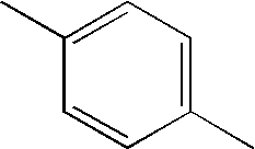


(A-13) 


(A-14) 


(A-15) 


(A-16) 


(A-17) 


(A-18) 


(A-19) 


(A-20) 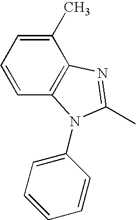


(A-21) 

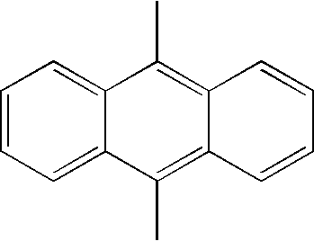

(A-22) 


(A-23) 


(A-24) 


(A-25) 


(A-26) 


(A-27) 


(A-28) 


(A-29) 


(A-30) 


(A-31) 


(A-32) 


(A-33) 


(A-34) 


(A-35) 


(A-36) 


(A-37) 


(A-38) 


(A-39) 


(A-40) 


(4-41) 


(B-1) 


(B-2) 


(B-3) 


- When L represents a linking group having a functionality of two or greater, general formula (A) or (B) is preferably represented by HAr -L′-Ar1-L′-HAr having a functionality of two or greater. Preferable examples of L′ or Ar1 is the same as the above examples, which may be substituted, and L′ may be single bonded.
- R or R′ represents hydrogen atom, an aliphatic hydrocarbon group, an aromatic hydrocarbon group or a heterocyclic group.
- The aliphatic hydrocarbon group represented by R or R′ is a linear, branched or cyclic alkyl group (an alkyl group preferably having 1 to 20 carbon atoms, more preferably having 1 to 12 carbon atoms and most preferably having 1 to 8 carbon atoms, such as methyl group, ethyl group, isopropyl group, t-butyl group, n-octyl group, n-decyl group, n-hexadecyl group, cyclopropyl group, cyclopentyl group and cyclohexyl group), an alkenyl group (an alkenyl group preferably having 2 to 20 carbon atoms, more preferably having 2 to 12 carbon atoms and most preferably having 2 to 8 carbon atoms, such as vinyl group, aryl group, 2-butenyl group and 3-pentenyl group), or an alkynyl group (an alkynyl group preferably having 2 to 20 carbon atoms, more preferably having 2 to 12 carbon atoms and most preferably having 2 to 8 carbon atoms, such as propargyl group and 3-pentynyl group). An alkyl group is preferable among these groups.
- The aromatic hydrocarbon group represented by R or R′ is a group having a single ring or a condensed ring, which is an aromatic hydrocarbon group preferably having 6 to 30 carbon atoms, more preferably having 6 to 20 carbon atoms and most preferably having 6 to 12 carbon atoms, such as phenyl group, 2-methylphenyl group, 3-methylphenyl group, 4-methylphenyl group, 2-methoxyphenyl group, 3-trifluoromethylphenyl group, pentafluorophenyl group, 1-naphthyl group and 2-naphthyl group.
- The heterocyclic group represented by R or R′ has a single ring or a condensed ring, preferably has 1 to 20 carbon atoms, more preferably having 1 to 12 carbon atoms and most preferably having 2 to 10 carbon atoms and is preferably an aromatic heterocyclic group having at least one of nitrogen atom, oxygen atom, sulfur atom and selenium atom. Examples of the heterocyclic group include groups derived from pyrrolidine, piperidine, piperazine, morpholine, thiophene, selenophene, furan, pyrrol, imidazole, pyrazole, pyridine, pyrazine, pyridazine, pyrimidine, triazole, triazine, indole, indazole, purine, thiazoline, thiazole, thiadiazole, oxazoline, oxazole, oxadiazole, quinoline, isoquinoline, phthalazine, naththylidine, quinoxaline, quinazoline, cinnoline, puteridine, acridine, phenanthroline, phenazine, tetrazole, benzimidazole, benzoxazole, benzothiazole, benzotriazole, tetrazaindene, carbazole and azepine. Groups derived from furan, thiophene, pyridine, pyrazine, pyrimidine, pyridazine, triazine, quinoline, phthalazine, naphthylidine, quinoxaline and quinazoline are preferable, and groups derived from quinoline are more preferable.
- The aliphatic hydrocarbon group, the aromatic hydrocarbon group and the heterocyclic group which are represented by R or R′ may have substituents. Examples of the substituent include the substituents described as the examples of the substituent to the group represented by L. Preferable examples of the substituent include the substituents described as the preferable examples of the substituent to the group represented by L.
- It is preferable that R or R′ represents an aliphatic hydrocarbon group, an aromatic hydrocarbon group or a heterocyclic group. It is more preferable that R or R′ represents an aliphatic hydrocarbon group (preferably having 6 to 30 carbon atoms, more preferably having 6 to 20 carbon atoms and most preferably having 6 to 12 carbon atoms) or an aromatic hydrocarbon. It is most preferable that R or R′ represents an aliphatic hydrocarbon group (preferably having 1 to 20 carbon atoms, more preferably having 1 to 12 carbon atoms and most preferably having 2 to 10 carbon atoms).
- n represents an integer of one or two.
- Further, among the compounds with a ring structure and having nitrogen atom as the electron transporting material, those with imidazopyridine structure are represented by following general formula (C).

- In the above general formula (C), Ar1′ represents a substituted or unsubstituted aryl group having 6 to 60 nuclear carbon atoms (preferably having 6 to 40 nuclear carbon atoms) or a substituted or unsubstituted heteroaryl group having 3 to 60 nuclear carbon atoms (preferably having 3 to 40 nuclear carbon atoms).
- Examples of the substituted or unsubstituted aryl group represented by Ar1′ include phenyl group, 1-naphthyl group, 2-naphthyl group, 1-anthryl group, 2-anthryl group, 9-anthryl group, 1-phenanthryl group, 2-phenanthryl group, 3-phenanthryl group, 4-phenanthryl group, 9-phenanthryl group, 1-naphthacenyl group, 2-naphthacenyl group, 9-naphthacenyl group, 1-chrysenyl group, 2-chrysenyl group, 6-chrysenyl group, 1-pyrenyl group, 2-pyrenyl group, 4-pyrenyl group, 2-biphenylyl group, 3-biphenylyl group, 4-biphenylyl group, p-terphenyl-4-yl group, p-terphenyl-3-yl group, p-terphenyl-2-yl group, m-terphenyl-4-yl group, m-terphenyl-3-yl group, m-terphenyl-2-yl group, o-tolyl group, m-tolyl group, p-tolyl group, p-t-butylphenyl group, p-(2-phenylpropyl)phenyl group, 3-methyl-2-naphthyl group, 4-methyl-1-naphthyl group, 4-methyl-1-anthryl group, 4′-methylbiphenylyl group, 4″-t-butyl-p-terphenyl-4-yl group, fluoranthenyl group, fluorenyl group, monovalent groups having the spirofluorene structure, perfluorophenyl group, perfluoronaphthyl group, perfluoroanthryl group, perfluorobiphenylyl group, monovalent groups having the 9-phenylanthancene structure, monovalent groups having the 9-(1′-naphthyl)anthracene structure, monovalent groups having the 9-(2′-naphthyl)anthracene structure, monovalent groups having the 6-phenylchrysene structure and monovalent groups having the 9-[4-(diphenylamino)phenyl]anthracene structure. Among these groups, phenyl group, naphthyl groups, biphenyl groups, terphenyl groups, 9-(10-phenyl)anthryl group, 9-[10-(1′-naphthyl)]anthryl group and 9-[10-(2′-naphthyl)]anthryl group are preferable.
- Examples of the substituted or unsubstituted heteroaryl group represented by Ar1′ include pyrrolyl group, furyl group, thienyl group, silacyclopentadienyl group, pyridyl group, quinolyl group, isoquinolyl group, benzofuryl group, imidazolyl group, pyrimidyl group, carbazolyl group, selenophenyl group, oxadiazolyl group and triazolyl group. Among these groups, pyridyl group, quinolyl group and isoquinolyl group are preferable.
- In general formula (C), Ar2′ represents hydrogen atom, a substituted or unsubstituted aryl group having 6 to 60 nuclear carbon atoms (preferably having 6 to 40 nuclear carbon atoms), a substituted or unsubstituted heteroaryl group having 3 to 60 nuclear carbon atoms (preferably having 3 to 40 nuclear carbon atoms), a substituted or unsubstituted alkyl group having 1 to 20 nuclear carbon atoms (preferably having 1 to 6 carbon atoms) or a substituted or unsubstituted alkoxyl group having 1 to 20 nuclear carbon atoms (preferably having 1 to 6 carbon atoms).
- Examples of the substituted or unsubstituted aryl group represented by Ar2′ include the groups described above as the examples of the substituted or unsubstituted aryl group represented by Ar1′.
- Examples of the substituted or unsubstituted heteroaryl group represented by Ar2′ include the groups described above as the examples of the substituted or unsubstituted heteroaryl group represented by Ar1′.
- Examples of the substituted or unsubstituted alkyl group represented by Ar2′ include methyl group, ethyl group, propyl group, isopropyl group, n-butyl group, s-butyl group, isobutyl group, t-butyl group, n-pentyl group, n-hexyl group, n-heptyl group, n-octyl group, hydroxymethyl group, 1-hydroxyethyl group, 2-hydroxyethyl group, 2-hydroxyisobutyl group, 1,2-dihydroxyethyl group, 1,3-dihydroxy-isopropyl group, 2,3-dihydroxy-t-butyl group, 1,2,3-trihydroxypropyl group, chloromethyl group, 1-chloroethyl group, 2-chloroethyl group, 2-chloroisobutyl group, 1,2-dichloroethyl group, 1,3-dichloroisopropyl group, 2,3-dichloro-t-butyl group, 1,2,3-trichloropropyl group, bromomethyl group, 1-bromoethyl group, 2-bromoethyl group, 2-bromoisobutyl group, 1,2-dibromoethyl group, 1,3-dibromoisopropyl group, 2,3-dibromo-t-butyl group, 1,2,3-tribromopropyl group, iodomethyl group, 1-iodoethyl group, 2-iodoethyl group, 2-iodoisobutyl group, 1,2-diiodoethyl group, 1,3-diiodoisopropyl group, 2,3-diiodo-t-butyl group, 1,2,3-triiodopropyl group, aminomethyl group, 1-aminoethyl group, 2-aminoethyl group, 2-aminoisobutyl group, 1,2-diaminoethyl group, 1,3-diaminoisopropyl group, 2,3-diamino-t-butyl group, 1,2,3-triaminopropyl group, cyanomethyl group, 1-cyanoethyl group, 2-cyanoethyl group, 2-cyanoisobutyl group, 1,2-dicyanoethyl group, 1,3-dicyanoisopropyl group, 2,3-dicyano-t-butyl group, 1,2,3-tricyanopropyl group, nitromethyl group, 1-nitroethyl group, 2-nitroethyl group, 2-nitroisobutyl group, 1,2-dinitroethyl group, 1,3-dinitroisopropyl group, 2,3-dinitro-t-butyl group, 1,2,3-trinitropropyl group, cyclopropyl group, cyclobutyl group, cyclopentyl group, cyclohexyl group, 4-methylcyclohexyl group, 1-adamantyl group, 2-adamantyl group, 1-norbornyl group and 2-norbornyl group. Among these groups, methyl group, ethyl group and t-butyl group are preferable.
- In general formula (C), the substituted or unsubstituted alkoxyl group represented by Ar2′ is a group represented by OY. Examples of the group represented by Y include methyl group, ethyl group, propyl group, isopropyl group, n-butyl group, s-butyl group, isobutyl group, t-butyl group, n-pentyl group, n-hexyl group, n-heptyl group, n-octyl group, hydroxymethyl group, 1-hydroxyethyl group, 2-hydroxyethyl group, 2-hydroxyisobutyl group, 1,2-dihydroxyethyl group, 1,3-dihydroxyisopropyl group, 2,3-dihydroxy-t-butyl group, 1,2,3-trihydroxypropyl group, chloromethyl group, 1-chloroethyl group, 2-chloroethyl group, 2-chloroisobutyl group, 1,2-dichloroethyl group, 1,3-dichloroisopropyl group, 2,3-dichloro-t-butyl group, 1,2,3-trichloropropyl group, bromomethyl group, 1-bromoethyl group, 2-bromoethyl group, 2-bromoisobutyl group, 1,2-dibromoethyl group, 1,3-dibromoisopropyl group, 2,3-dibromo-t-butyl group, 1,2,3-tribromopropyl group, iodomethyl group, 1-iodoethyl group, 2-iodoethyl group, 2-iodoisobutyl group, 1,2-diiodoethyl group, 1,3-diiodoisopropyl group, 2,3-diiodo-t-butyl group, 1,2,3-triiodopropyl group, aminomethyl group, 1-aminoethyl group, 2-aminoethyl group, 2-aminoisobutyl group, 1,2-diaminoethyl group, 1,3-diaminoisopropyl group, 2,3-diamino-t-butyl group, 1,2,3-triaminopropyl group, cyanomethyl group, 1-cyanoethyl group, 2-cyanoethyl group, 2-cyanoisobutyl group, 1,2-dicyanoethyl group, 1,3-dicyanoisopropyl group, 2,3-dicyano-t-butyl group, 1,2,3-tricyanopropyl group, nitromethyl group, 1-nitroethyl group, 2-nitroethyl group, 2-nitroisobutyl group, 1,2-dinitroethyl group, 1,3-dinitroisopropyl group, 2,3-dinitro-t-butyl group and 1,2,3-trinitropropyl group. Among these groups, methyl group, ethyl group and t-butyl group are preferable.
- In general formula (C), at least one of the groups represented by Ar1′ and Ar2′ is a substituted or unsubstituted condensed cyclic group having 10 to 60 nuclear carbon atoms or a substituted or unsubstituted condensed mono-heterocyclic group having 3 to 60 nuclear carbon atoms.
- In general formula (C), L1 and L2 each independently represent the single bond, a substituted or unsubstituted arylene group having 6 to 60 nuclear carbon atoms (preferably having 6 to 40 nuclear carbon atoms), a substituted or unsubstituted heteroarylene group having 3 to 60 nuclear carbon atoms (preferably having 3 to 40 nuclear carbon atoms) or a substituted or unsubstituted fluorenylene group.
- Examples of the substituted or unsubstituted arylene group represented by L1 or L2 include divalent groups formed by removing hydrogen atom from the aryl groups described above as the examples of the substituted or unsubstituted aryl group represented by the above Ar1′.
- Examples of the substituted or unsubstituted heteroarylene group represented by L1 or L2 include divalent groups formed by removing hydrogen atom from the heteroaryl groups described above as the examples of the substituted or unsubstituted heteroaryl group represented by the above Ar1′.
- In general formula (C), it is preferable that L1 and/or L2 represent a group selected from the group consisting of the following:

- It is preferable that, in general formula (C), Ar1′ represents a group represented by one of the following general formulae (a) to (j):


wherein R1 to R92 each independently represent hydrogen atom, a halogen atom, a substituted or unsubstituted alkyl group having 1 to 20 carbon atoms, a substituted or unsubstituted alkoxyl group having 1 to 20 carbon atoms, a substituted or unsubstituted aryloxyl group having 6 to 40 nuclear carbon atoms, a substituted or unsubstituted diarylamino group having 12 to 80 nuclear carbon atoms, a substituted or unsubstituted aryl group having 6 to 40 nuclear carbon atoms, a substituted or unsubstituted heteroaryl group having 3 to 40 nuclear carbon atoms or a substituted or unsubstituted diarylamino group having 18 to 120 nuclear carbon atoms, and L3 represents the single bond or a group selected from the following groups:
- In the foregoing general formula (C), R″ represents hydrogen atom, a substituted or unsubstituted aryl group having 6 to 60 nuclear carbon atoms, a substituted or unsubstituted heteroaryl group having 3 to 60 nuclear carbon atoms, a substituted or unsubstituted alkyl group having 1 to 20 carbon atoms or a substituted or unsubstituted alkoxyl group having 1 to 20 carbon atoms.
- Examples of the substituted or unsubstituted aryl group represented by R″ include the groups described above as the examples of the substituted or unsubstituted aryl group represented by the foregoing Ar1′.
- Examples of the substituted or unsubstituted heteroaryl group represented by R″ include the groups described above as. the examples of the substituted or unsubstituted heteroaryl group represented by the foregoing Ar1′.
- Examples of the substituted or unsubstituted alkyl group represented by R″ include the groups described above as the examples of the substituted or unsubstituted alkyl group represented by the foregoing Ar2′.
- Examples of the substituted or unsubstituted alkoxyl group represented by R″ include the groups described above as the examples of the substituted or unsubstituted alkoxyl group represented by the foregoing Ar2′.
- It is preferable that the five-membered cyclic derivative with a ring having nitrogen atom which is represented by general formula (C) has one of the basic skeleton structures shown in the following as the examples. However, the basic skeleton structure is not limited to those shown as the example.

Ar1 L1 L2 Ar2 (C-1) 


(C-2) 


(C-3) 


(C-4) 


(C-5) 


(C-6) 


(C-7) 


(C-8) 


(C-9) 


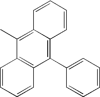
(C-10) 


(C-11) 


(C-12) 


(C-13) 


(C-14) 


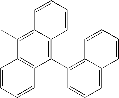
(C-15) 


(C-16) 


(C-18) 


(C-17) 


(C-19) 


(C-20) 


3-1 


(C-21) 


(C-22) 


(C-23) 


(C-24) 


(C-25) 


(C-26) 


(C-27) 


(C-28) 


(C-29) 


(C-30) 


(C-31) 


(C-32) 


(C-33) 


(C-34) 


(C-35) 


(C-36) 


(C-37) 


(C-38) 


(C-39) 


- The compound with a ring having a nitrogen atom represented by the foregoing general formula (C) may have substituents. As the substituent, alkyl groups, alkenyl groups, alkynyl groups, aromatic hydrocarbon groups, amino group, alkoxyl groups, aryloxyl groups, acyl groups, alkoxycarbonyl groups, aryloxycarbonyl groups, acyloxyl groups, acylamino groups, alkoxycarbonylamino groups, aryloxycarbonylamino groups, sulfonylamino groups, sulfamoyl groups, carbamoyl groups, alkylthio groups, alkylthio groups, arylthio groups, sulfonyl group, halogen atoms, cyano group and aromatic heterocyclic groups are preferable. Alkyl groups, aryl groups, alkoxyl groups, aryloxyl groups, halogen atoms, cyano group and aromatic heterocyclic group are more preferable. Alkyl groups, aryl groups, alkoxyl groups, aryloxyl groups and aromatic heterocyclic groups are still more preferable, and alkyl groups, aryl groups, alkoxyl groups and aromatic heterocyclic groups are most preferable.
- These compounds with a ring having a nitrogen atom are superior in electron injecting capability from the cathode because their energy gaps are small, superior in durability of electron transporting and enable to provide the EL device of long lifetime.
- In the present invention, it is preferable that the reductive dopant is added in either the electron injecting layer or the interfacial zone between the cathode and the layer adhered to the cathode, and that the work function of the reductive dopant is 2.9 eV or smaller. The reductive dopant used in the present invention is defined as a compound which is added to the interfacial zone between the electron injecting layer and the cathode and which enhances the effectiveness in electron injecting. At least a portion of the organic layer comprised in the interfacial zone is reduced to form anions.
- As for the addition form of the reductive dopant, it is preferable that the reductive dopant is added in a manner such that a layer or islands are formed in the interfacial zone described above.
- Examples of the reductive dopant include at least one compound selected from alkali metals, alkali metallic complexes, alkali metal compounds, alkaline earth metals, alkaline earth metallic complexes, alkaline earth metal compounds, rare earth metals, rare earth metallic complexes and rare earth metal compounds. Examples of the alkali metal compound, the alkaline earth metal compound and the rare earth metal compound described above include oxides and halides of the respective metals.
- Examples of the alkali metal include Na (the work function: 2.36 eV), K (the work function: 2.28 eV), Rb (the work function: 2.16 eV) and Cs (the work function: 1.95 eV). Alkali metals having a work function of 2.9 eV or smaller are preferable. Among these alkali metals, K, Rb and Cs are preferable, Rb and Cs are more preferable, and Cs is most preferable.
- Examples of the alkaline earth metal include Ca (the work function: 2.9 eV), Sr (the work function: 2.0 to 2.5 eV) and Ba (the work function: 2.52 eV). Alkaline earth metals with a work function of 2.9 eV or smaller are preferable.
- Examples of the rare earth metal include Sc, Y, Ce, Tb and Yb. Rare earth metals with a work function of 2.9 eV or smaller are preferable.
- When the preferable metals among the above metals are used, the luminance of the emitted light and the lifetime of the organic EL device can be increased by addition of the metals into the electron injecting layer in a relatively small amount since these metals have great reducing ability.
- Examples of the alkali metal compound described above include alkali metal oxides such as Li2O, CS2O and K2O and alkali metal halides such as LiF, NaF, CsF and KF. Among these compounds, alkali metal oxides and alkali metal fluorides such as LiF, Li2O and NaF are preferable.
- Examples of the alkaline earth metal compound described above include BaO, SrO, CaO and mixtures thereof such as BaxSr1-xO (O<x<1) and BaxCa1-xO (O<x<1). Among these compounds, BaO, SrO and CaO are preferable.
- Examples of the rare earth metal compound described above include YbF3, ScF3, ScO3, Y2O3, Ce2O3, GdF3 and TbF3. Among these compounds, YbF3, ScF3 and TbF3 are preferable.
- The alkali metallic complex, the alkaline earth metallic complex and the rare earth metallic complex are not particularly limited as long as the complexes contain at least one of the alkali metal ions, the alkaline earth metal ions and rare earth metal ions, respectively, as the metal ion. As the ligand, quinolinol, benzoquinolinol, acridinol, phenanthridinol, hydroxyphenyloxazole, hydroxyphenylthiazole, hydroxydiaryloxadiazoles, hydroxydiarylthiadiazoles, hydroxyphenylpyridine, hydroxyphenylbenzimidazole, hydroxybenzotriazole, hydoxyflavone, bipyridyl, phenanthroline, phthalocyanine, porphyrin, cyclopentadiene, β-diketones, azomethines and derivatives of these compounds are preferable. However, the ligand is not limited to the ligands described above.
- As the process for adding the reductive dopant, it is preferable that an organic material which is the light emitting material or the electron injecting material forming the interfacial zone is vaporized while the reductive dopant is simultaneously vapor deposited in accordance with the resistance heating deposition method so that the reductive dopant is dispersed in the organic material. The concentration of the dispersion expressed as the ratio of the amounts by mole of the organic substance to the reductive dopant is in the range of 100:1 to 1:100 and preferably in the range of 5:1 to 1:5.
- When the reductive dopant is added to form a layer, the reductive dopant alone is vapor deposited in accordance with the resistance heating deposition method to form a layer preferably having a thickness of 0.1 to 15 nm after a layer of the organic material such as the light emitting material and the electron injecting material is formed as the interfacial zone.
- When the reductive dopant is added to form islands, the reductive dopant alone is vapor deposited in accordance with the resistance heating deposition method to form islands preferably having a thickness of 0.1 to 15 nm after islands of the organic material such as the light emitting material and the electron injecting material were formed as the interfacial zone.
- It is preferable that the relative amounts by mole of the main component and the reductive dopant in the electron injecting layer of the organic EL device of the present invention is in the range of 5:1 to 1:5 and more preferably in the range of 2:1 to 1:2.
- In the organic EL device of the present invention, a hole transporting layer in which a phosphorescent light emitting material is added may be preferably sandwiched between the cathode and the anode. Further, it is preferable that the triplet energy of the hole transporting material in the hole transporting layer is greater than the excitation energy of the phosphorescent light emitting material in the light emitting layer.
- Moreover, the conventional TPD or NPD below has triplet energy of 2.46 eV or 2.51 eV respectively, whereas the foregoing (K-10) on page 18 as the phosphorescent light emitting material in the light emitting layer has triplet energy of 2.55 eV.

- Accordingly, TPD or NPD above quenches the excited state of the light emitting layer. In other words, a hole transporting material whose triplet energy is greater than 2.55 eV or regulates quenching and enhances efficiency of light emission.
- Specific examples of the hole transporting material having triplet energy of greater than 2.55 eV employed in the present invention include compounds below each represented by the following general formulae (10), (12), (14) to (17) and (19), each of which is preferably without having any condensed aromatic ring.
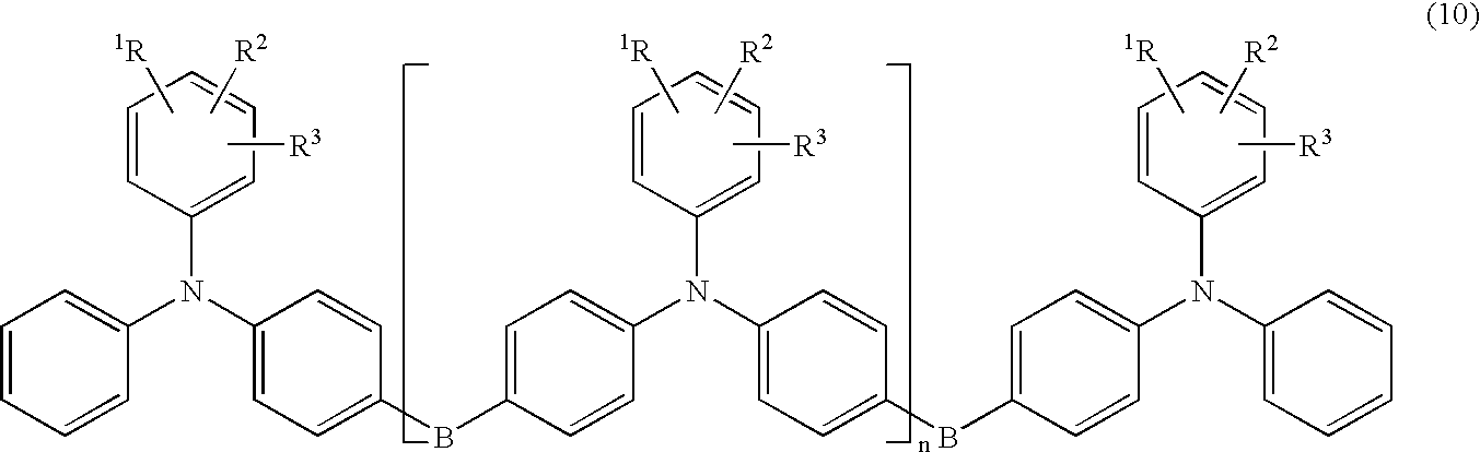
wherein n represents an integer of 0 to 3, R1 to R3 each independently represents a substituted or unsubstituted alkyl group having 1 to 30 carbon atoms, a substituted or unsubstituted alkoxyl group having 1 to 30 carbon atoms, a substituted or unsubstituted aryl group having 6 to 30 carbon atoms and a substituted or unsubstituted arylalkyl group having 6 to 30 carbon atoms, B represents an aliphatic ring residue group such as cyclohexylene or adamanthyl, and preferably represents an aliphatic ring residue group represented by the following general formula (11):
wherein Y represents a substituted or unsubstituted alkyl group or a substituted or unsubstituted aryl group, n represents an integer of 2 to 7, and m represents an integer of 0 to 2.
A-B-A (12)
wherein A represents a diamine derivative residue group represented by the general formula (13) below, B represents an adamanthyl aliphatic cyclic group and preferably represents the aliphatic ring residue group represented by the foregoing general formula (11).
wherein R1 to R9 each independently represent a hydrogen atom, a halogen atom, a substituted or unsubstituted alkyl group, a substituted or unsubstituted alkoxyl group, a substituted or unsubstituted tio alkoxyl group, cyano group, amino group, mono- or di-substituted amino group, hydroxyl group, mercapto group, a substituted or unsubstituted aryloxy group, a substituted or unsubstituted arylthio group, a substituted or unsubstituted aromatic ring group or a substituted or unsubstituted heterocyclic group. However, at least any one of R1 to R3, R4 to R6 and R7 to R9 is not a hydrogen atom. Further, adjacent substituted groups may bond to form a substituted or unsubstituted ring of aliphatic group, a substituted or unsubstituted ring of carbon ring aromatic group, a substituted or unsubstituted ring of heterocyclic aromatic group, or a substituted or unsubstituted heterocyclic ring. X represents phenyl, biphenyl-yl or terphenyl-yl.
wherein Ar6 to Ar9 each independently represents an unsubstituted aromatic group or an aromatic group having 6 to 18 carbon atoms and substituted with alkyl group or alkoxyl group all of which may be the same or different each other; at least one among Ar6 to Ar9 is preferably biphenyl group or terphenyl group; X represents single bond or a divalent group comprising phenylene, biphenyl-yl, N-alkyl or N-arylcarvazole. - A diamine compound represented by:

wherein Ar1 and Ar2 each independently represents a substituted or unsubstituted aryl group having 6 to 18 nuclear carbon atoms; R represents a substituted or unsubstituted alkyl group having 1 to 30 carbon atoms, a substituted or unsubstituted al k oxyl group, or a substituted or unsubstituted aryl group having 6 to 18 nuclear carbon atoms. X represents single bond, or a bonding group represented by alkylene, —O═or ═S═; and X may be present or absent. - A triamine compound represented by:

wherein Ar1 represents a substituted or unsubstituted aryl group having 6 to 18 nuclear carbon atoms; Ar2 to Ar5 each independently represents a substituted or unsubstituted arylene group having 6 to 18 nuclear carbon atoms; X represents single bond, or a bonding group represented by alkylene, —O— or —S—; which may be present or absent; X2 and X3 each independently represents single bond, or a bonding group represented by alkylene, —O— or —S—, and which may be the same or different each other.
wherein R1 to R12 each independently represent hydrogen atom, a halogen atom, alkyl group, aralkyl group, alkenyl group, cyano group, amino group, acyl group, alkoxycarbonyl group, carboxyl group, an alkoxy group, alkylamino group, aralkyl amino group, haloalkyl group, hydroxy group, aryloxy group, a substituted or unsubstituted aromatic hydrocarbon group, or a substituted or unsubstituted aromatic heterocyclic group; and adjacent substituted groups of R1 and R2, R3 and R4, R5 and R6, R7 and R8, R9 and R10 or R11 and R12 may bond to form a ring. - X represents trivalent bonding group represented by the following:

wherein Ar1 represents a substituted or unsubstituted aromatic heterocyclic hydrocarbon group, a substituted or unsubstituted aromatic heterocyclic group or a group represented by the following general formula
wherein R13 to R18 each independently represent hydrogen atom, a halogen atom, alkyl group, aralkyl group, alkenyl group, cyano group, a substituted or unsubstituted amino group, acyl group, alkoxycarbonyl group, carboxyl group, an alkoxyl group, alkyl amino group, aralkyl amino group, haloalkyl group, hydroxyl group, aryloxy group, a substituted or unsubstituted aromatic hydrocarbon group, or a substituted or unsubstituted aromatic heterocyclic group; and adjacent substituted groups of R13 and R14, R15 and R16, or R17 and R18 may bond to form a ring.
wherein R represents alkyl group, aralkyl group, a substituted or unsubstituted amino group, acyl group, alkoxycarbonyl group, carboxyl group, an alkoxyl group, alkylamino group, aralkyl amino group, haloalkyl group, hydroxyl group, aryloxy group, a substituted or unsubstituted aromatic hydrocarbon group, or a substituted or unsubstituted aromatic heterocyclic group. - Typical examples of the construction of the organic EL device include an anode/a light emitting layer/an electron injecting layer/a cathode; an anode/a hole injecting layer/a light emitting layer/an electron injecting layer/a cathode; an anode/a hole injecting layer/a hole transporting layer/a light emitting layer/an electron injecting layer/a cathode; and an anode/an insulating layer/a hole injecting layer/a hole transporting layer/a light emitting layer/an electron injecting layer/a cathode.
- In the organic EL device of the present invention, an electron transporting layer formed with an insulating material or a semiconductor may be further sandwiched between the cathode and the organic thin film layer. The electron transporting layer effectively prevents leak in the electric current and improves the electron injecting capability.
- It is preferable that at least one metal compound selected from the group consisting of alkali metal chalcogenides, alkaline earth metal chalcogenides, alkali metal halides and alkaline earth metal halides is used as the insulating material. It is preferable that the electron transporting layer is constituted with the above alkali metal chalcogenide since the electron injecting property can be improved. Preferable examples of the alkali metal chalcogenide include Li2O, LiO, Na2S, Na2Se and NaO. Preferable examples of the alkaline earth metal chalcogenide include CaO, BaO, SrO, BeO, BaS and CaSe. Preferable examples of the alkali metal halide include LiF, NaF, KF, LiCl, KCl and NaCl. Preferable examples of the alkaline earth metal halide include fluorides such as CaF2, BaF2, SrF2, MgF2 and BeF2 and halides other than the fluorides.
- Examples of the semiconductor constituting the electron transporting layer include oxides, nitrides and oxide nitrides containing at least one element selected from Ba, Ca, Sr, Yb, Al, Ga, In, Li, Na, Cd, Mg, Si, Ta, Sb and Zn, which are used singly or in combination of two or more. It is preferable that the inorganic compound constituting the electron transporting layer is in the form of a fine crystalline or amorphous insulating thin film. When the electron transporting layer is constituted with the above insulating thin film, a more uniform thin film can be formed and defective pixels such as dark spots can be decreased. Examples of the inorganic compound include the alkali metal chalcogenides, the alkaline earth metal chalcogenides, the alkali metal halides and the alkaline earth metal halides which are described above.
- The hole injecting layer and the hole transporting layer are layers which help injection of holes into the light emitting layer and transport holes to the light emitting zone. The layers exhibit a great mobility of holes and, in general, have an ionization energy as small as 5.5 eV or smaller. For the hole injecting layer and the hole transporting layer, a material which transports holes to the light emitting layer under a small strength of the electric field is preferable. A material which exhibits, for example, a mobility of holes of at least 10−6 cm2/V second under application of an electric field of 104 to 106 V/cm is preferable. The mobility of holes of at least 10−5 cm2V-second under application of an electric field of 104 to 106 V/cm is more preferable
- The anode of the organic EL device plays the role of injecting holes into the hole transporting layer or the light emitting layer. It is effective that the anode has a work function of 4.5 eV or greater. Examples of the material of the anode used in the present invention include indium tin oxide alloys (ITO), tin oxides (NESA), gold, silver, platinum and copper. As the cathode, a material having a small work function is preferable so that electrons can be injected into the electron transporting layer or the light emitting layer. The material of the cathode is not particularly limited. Examples of the material of the cathode include indium, aluminum, magnesium, magnesium-indium alloys, magnesium-aluminum alloys, aluminum-lithium alloys, aluminum-scandium-lithium alloys and magnesium-silver alloys.
- The process for forming the layers in the organic EL device of the present invention is not particularly limited. A conventional process such as the vacuum vapor deposition process and the spin coating process can be used. The organic thin film layer used in the organic EL device of the present invention can be formed in accordance with the vacuum vapor deposition process, the molecular beam epitaxy process (the MBE process) or, using a solution prepared by dissolving the compound into a solvent, in accordance with a conventional coating process such as the dipping process, the spin coating process, the casting process, the bar coating process and the roller coating process.
- The thickness of each layer in the organic thin film layer in the organic EL device of the present invention is not particularly limited. In general, an excessively thin layer tends to have defects such as pin holes, and an excessively thick layer requires a high applied voltage results in decreasing the efficiency. Therefore, a thickness within the range of several nanometers to 1 μm is preferable.
- The present invention will be described more specifically with reference to examples in the following. However, the present invention is not limited to the examples.
- The triplet energy gap, the single energy gap and the ionization potential of a compound were measured in accordance with the following methods.
- (1) Measurement of the Triplet Energy Gap
- The lowest excited triplet energy level T1 was measured. The phosphorescence spectrum of a sample was measured (10 μmoles/liter; an EPA (diethyl ether:isopentane:ethanol=5:5:2 by volume) solution; 77K; a quartz cell; FLUOROLOGII manufactured by SPEX Company). A tangent was drawn to the increasing line at the short wavelength side of the phosphorescence spectrum and the wavelength at the intersection of the tangent and the abscissa (the end of light emission) was obtained. The obtained wavelength was converted into the energy.
- (2) Measurement of the Singlet Energy Gap
- The excited singlet energy gap was measured. Using a toluene solution (10−5 moles/liter) of a sample, the absorption spectrum was obtained by a spectrometer for absorption of ultraviolet and visible light manufactured by HITACHI Co. Ltd. A tangent was drawn to the increasing line at the long wavelength side of the spectrum and the wavelength at the intersection of the tangent and the abscissa (the end of absorption) was obtained. The obtained wavelength was converted into the energy.
- (3) Measurement of the Ionization Potential
- The ionization potential of the compound was measured by means of photoelectron spectroscopy instrument: AC-1 produced by Riken Keiki Co., Ltd. using powder material as the object to be measured under the atmosphere of the air.
- A glass substrate (manufactured by GEOMATEC Company) of 25 mm×75 mm×1.1 mm thickness having an ITO transparent electrode was cleaned by application of ultrasonic wave in isopropyl alcohol for 5 minutes and then by exposure to ozone generated by ultraviolet light for 30 minutes. The glass substrate having the transparent electrode which had been cleaned was adhered to a substrate holder of a vacuum vapor deposition apparatus. On the surface of the cleaned substrate at the side having the transparent electrode, a film of copper phthalocyanine (referred to as a film of CuPc, hereinafter) having a thickness of 10 nm was formed in a manner such that the formed film covered the transparent electrode. The formed film of CuPc worked as the hole injecting layer. On the formed film of CuPc, a film of 1,1′-bis[4-N,N-di(p-tolyl)aminophenyl]cyclohexane shown below (referred to as a film of TPAC, hereinafter) having a thickness of 30 nm was formed. The formed film of TPAC worked as the hole transporting layer. On the formed film of TPAC, a film of a compound PB102 shown below having a thickness of 30 nm was formed by vapor deposition as the light emitting layer. At the same time, the foregoing phosphorescent Ir metallic complex (K-3) on page 17 was added to the light emitting layer. The content of the Ir metallic complex (K-3) in the light emitting layer was 7% by weight. The formed film of (K-3) worked as the light emitting layer. On the formed film of (K-3), a film of a complex of tris(8-quinolinolato)aluminum (Alq) was formed by vapor deposition. The formed film of Alq worked as the electron injecting layer. Thereafter, Li (the source of lithium: manufactured by SAES GETTERS Company) as the reductive dopant and Alq were binary vapor deposited and an Alq:Li film having a thickness of 10 nm was formed as the second electron injecting layer (the cathode). On the formed Alq:Li film, metallic aluminum was vapor deposited to form a metal cathode and an organic EL device was prepared.
- The host materials in the light emitting layer, their ionization potential, their energy gap (singlet energy) and their triplet energy, the phosphorescent light emitting materials in the light emitting layer (metallic complex) and their triplet energy, the electron transporting materials in the electron injecting layer, their energy gap and their triplet energy and materials of the hole transport layer are shown in Table 1.
- When a direct current voltage of 6.6 V was applied to the organic EL device prepared above, bluish green light was emitted with a luminance of 89 cd/m2 and a current efficiency of 15.0 cd/A. Further, by measuring EL spectrum, it was found that the light emitting peak wavelength was 477 nm exhibiting that Ir metallic complex caused light emission. The results are shown in Table 1. In the Examples, although the energy gap of Alq employed for the electron injecting layer was smaller than that of the host material or of Ir complex each in the light emitting layer, and although the triplet energy of Alq employed for the the electron injecting layer was smaller than that of the host material or of Ir complex each in the light emitting layer, the prepared organic EL devices revealed highly efficient light emission of bluish green at low voltage as will be described below.

- A glass substrate (manufactured by GEOMATEC Company) of 25 mm×75 mm×1.1 mm thickness having an ITO transparent electrode was cleaned by application of ultrasonic wave in isopropyl alcohol for 5 minutes and then by exposure to ozone generated by ultraviolet light for 30 minutes. The glass substrate having the transparent electrode which had been cleaned was adhered to a substrate holder of a vacuum vapor deposition apparatus. On the surface of the cleaned substrate at the side having the transparent electrode, a film of copper phthalocyanine (referred to as a film of CuPc, hereinafter) having a thickness of 10 nm was formed in a manner such that the formed film covered the transparent electrode. The formed film of CuPc worked as the hole injecting layer. On the formed film of CuPc, a film of the foregoing 4,4′-bis[N-(1-naphthyl)-N-phenylamino]biphenyl (a film of NPD) having a thickness of 30 nm was formed. The formed film of NPD worked as the hole transporting layer. On the formed film of NPD, a film having a thickness of 30 nm of a hole transportable compound CBP shown below as a host material was vapor deposited to form the light emitting layer. At the same time, the foregoing phosphorescent Ir metallic complex (K-3) on page 17 was added to the light emitting layer. The content of the Ir metallic complex (K-3) in the light emitting layer was 7% by weight. The formed film of (K-3) worked as the light emitting layer. On the formed film of (K-3), a film of (1,1′-bisphenyl)-4-olate)bis(2-methyl-8-quinolinolato) aluminum (referred to as a film of BAlq, hereinafter) having a thickness of 10 nm was formed. The formed film of BAlq worked as the hole blocking layer. Thereafter, Li (the source of lithium: manufactured by SAES GETTERS Company) as the reductive dopant and Alq were binary vapor deposited and an Alq:Li film having a thickness of 10 nm was formed as the second electron injecting layer (the cathode). On the formed Alq:Li film, metallic aluminum was vapor deposited to form a metal cathode and an organic EL device was prepared.
- The host materials in the light emitting layer, their ionization potential, their energy gap (singlet energy) and their triplet energy, the phosphorescent light emitting materials in the light emitting layer (metallic complex) and their triplet energy, the electron transporting materials in the electron injecting layer, their energy gap and their triplet energy and materials of the hole transport layer are shown in Table 1.
- When a direct current voltage of 7.2 V was applied to the organic EL device prepared above, bluish green light was emitted with a luminance of 98 cd/m2 and a current efficiency of 3.2 cd/A. This result appeared to be caused by deactivating the excitation state of the light emitting layer and by quenching light because the hole transporting compound was employed as the host material in the light emitting layer. The results are shown in Table 1.

- An organic EL device was prepared in a similar manner as Example 1 except that the above CBP with hole transporting capability was employed in place of the compound PB 102 as the host material in the light emitting layer.
- The host materials in the light emitting layer, their ionization potential, their energy gap (singlet energy) and their triplet energy, the phosphorescent light emitting materials in the light emitting layer (metallic complex) and their triplet energy, the electron transporting materials in the electron injecting layer, their energy gap and their triplet energy and materials of the hole transport layer are shown in Table 1.
- When a direct current voltage of 6.8 V was applied to the organic EL device prepared above, bluish green light was emitted with a luminance of 1.2 cd/m2 and a current efficiency of 0.3 cd/A. This result appeared to be caused by deactivating the excitation state of the light emitting layer and by quenching light because the hole transporting compound was employed as the host material in the light emitting layer. Further, it became clear by referring to Comparative Example 1, that a hole blocking layer is necessary in order to get a favorable efficiency of light emission. The results are shown in Table 1.
- An organic EL device was prepared in a similar manner as Example 1 except that PB 115 with electron transporting capability below was employed in place of the compound PB 102 as the host material in the light emitting layer.
- The host materials in the light emitting layer, their ionization potential, their energy gap (singlet energy) and their triplet energy, the phosphorescent light emitting materials in the light emitting layer (metallic complex) and their triplet energy, the electron transporting materials in the electron injecting layer, their energy gap and their triplet energy and materials of the hole transport layer are shown in Table 1.
- When a direct current voltage of 6.5 V was applied to the organic EL device prepared above, bluish green light was emitted with a luminance of 102 cd/m2 and a current efficiency of 14.8 cd/A. The results are shown in Table 1.

- An organic EL device was prepared in a similar manner as Example 1 except that the foregoing BAlq was employed in place of Alq and Alq:Li forming the electron injecting layer, and that Li was added at 20 nm in the cathode side of BAlq. In this case, the light emitting layer directly adheres with the electron injecting layer, and the cathode adheres with BAlq layer.
- The host materials in the light emitting layer, their ionization potential, their energy gap (singlet energy) and their triplet energy, the phosphorescent light emitting materials in the light emitting layer (metallic complex) and their triplet energy, the electron transporting materials in the electron injecting layer, their energy gap and their triplet energy and materials of the hole transport layer are shown in Table 1.
- When a direct current voltage of 7.8 V was applied to the organic EL device prepared above, bluish green light was emitted with a luminance of 93 cd/m2 and a current efficiency of 12.3 cd/A. The results are shown in Table 1.
- A glass substrate (manufactured by GEOMATEC Company) of 25 mm×75 mm×1.1 mm thickness having an ITO transparent electrode was cleaned by application of ultrasonic wave in isopropyl alcohol for 5 minutes and then by exposure to ozone generated by ultraviolet light for 30 minutes. The glass substrate having the transparent electrode which had been cleaned was adhered to a substrate holder of a vacuum vapor deposition apparatus. On the surface of the cleaned substrate at the side having the transparent electrode, a film of the foregoing NPD film having a thickness of 50 nm was formed in a manner such that the formed film covered the transparent electrode. The formed film of NPD worked as the hole transporting layer. On the formed film of NPD, a film having a thickness of 30 nm of an electron transportable compound PB115 shown above as a host material was vapor deposited to form the light emitting layer. At the same time, the foregoing phosphorescent Ir metallic complex (K-10) on page 18 was added to the light emitting layer. The content of the Ir metallic complex (K-10) in the light emitting layer was 5% by weight. The formed film of (K-10) worked as the light emitting layer. On the formed film of (K-10), a film of Alq was formed by vapor deposition. Thereafter, Li (the source of lithium: manufactured by SAES GETTERS Company) as the reductive dopant and Alq were binary vapor deposited and an Alq:Li film having a thickness of 30 nm was formed as the second electron injecting layer (the cathode). On the formed Alq:Li film, metallic aluminum was vapor deposited to form a metal cathode and an organic EL device was prepared.
- The host materials in the light emitting layer, their ionization potential, their energy gap (singlet energy) and their triplet energy, the phosphorescent light emitting materials in the light emitting layer (metallic complex) and their triplet energy, the electron transporting materials in the electron injecting layer, their energy gap and their triplet energy and materials of the hole transport layer are shown in Table 1.
- When a direct current voltage of 4.5 V was applied to the organic EL device prepared above, green light was emitted with a luminance of 620 cd/m2 and a current efficiency of 32.5 cd/A. The results are shown in Table 1.
- An organic EL device was prepared in a similar manner as Example 4 except that CBP with hole transporting capability above was employed in place of the compound PB 115 as the host material in the light emitting layer.
- The host materials in the light emitting layer, their ionization potential, their energy gap (singlet energy) and their triplet energy, the phosphorescent light emitting materials in the light emitting layer (metallic complex) and their triplet energy, the electron transporting materials in the electron injecting layer, their energy gap and their triplet energy and materials of the hole transport layer are shown in Table 1.
- When a direct current voltage of 5.1 V was applied to the organic EL device prepared above, green light was emitted with a luminance of 101 cd/m2 and a current efficiency of 5.7 cd/A.
- This result appeared to be caused by deactivating the excitation state of the light emitting layer and by quenching light because the hole transporting compound was employed as the host material in the light emitting layer. The results are shown in Table 1.
- An organic EL device was prepared in a similar manner as Example 4 except that BCP with electron transporting capability below was employed in place of the compound PB115 as the host material in the light emitting layer.
- The host materials in the light emitting layer, their ionization potential, their energy gap (singlet energy) and their triplet energy, the phosphorescent light emitting materials in the light emitting layer (metallic complex) and their triplet energy, the electron transporting materials in the electron injecting layer, their energy gap and their triplet energy and materials of the hole transport layer are shown in Table 1.
- When a direct current voltage of 6.2 V was applied to the organic EL device prepared above, green light was emitted with a luminance of 320 cd/m2 and a current efficiency of 30.2 cd/A, evading quench in the light emitting layer. However, it was necessary that the voltage was 1.7 V higher than that of the organic EL device in Example 4 in order to obtain the efficiency of light emission almost equal to the organic EL device in Example 4. This was caused by the prohibition of hole injection because the ionization potential of compound BCP is high. The results are shown in Table 1.

- An organic EL device was prepared in a similar manner as Example 2 except that TCTA below was employed as the material for the hole transporting layer in place of TPAC, that the foregoing (K-23) on page 20 was added as the phosphorescent Ir metallic complex in place of (K-3), and that the foregoing compound (A-7) on page 41 was employed as the electron transporting material in the electron injecting layer in place of Alq.
- The host materials in the light emitting layer, their ionization potential, their energy gap (singlet energy) and their triplet energy, the phosphorescent light emitting materials in the light emitting layer (metallic complex) and their triplet energy, the electron transporting materials in the electron injecting layer, their energy gap and their triplet energy and materials of the hole transport layer are shown in Table 1.
- When a direct current voltage of 6.0 V was applied to the organic EL device prepared above, bluish green light was emitted with a luminance of 104 cd/m2 and an extraordinarily enhanced efficiency of the light emission of 20.8 cd/A. The results are shown in Table 1.

- An organic EL device was prepared in a similar manner as Example 5 except that the foregoing compound (C-15) on page 57 was employed as the electron transporting material in the electron injecting layer in place of the compound (A-7) on page 41.
- The host materials in the light emitting layer, their ionization potential, their energy gap (singlet energy) and their triplet energy, the phosphorescent light emitting materials in the light emitting layer (metallic complex) and their triplet energy, the electron transporting materials in the electron injecting layer, their energy gap and their triplet energy and materials of the hole transport layer are shown in Table 1.
- When a direct current voltage of 6.1 V was applied to the organic EL device prepared above, bluish green light was emitted with a luminance of 105 cd/m2 and an extraordinarily enhanced efficiency of the light emission of 23.1 cd/A. The results are shown in Table 1.
- An organic EL device was prepared in a similar manner as Example 5 except that the foregoing compound CBP with hole transporting capability was employed in place of the compound PB115 as the host material in the light emitting layer.
- The host materials in the light emitting layer, their ionization potential, their energy gap (singlet energy) and their triplet energy, the phosphorescent light emitting materials in the light emitting layer (metallic complex) and their triplet energy, the electron transporting materials in the electron injecting layer, their energy gap and their triplet energy and materials of the hole transport layer are shown in Table 1.
- When a direct current voltage of 6.3 V was applied to the organic EL device prepared above, bluish green light was emitted with a luminance of 102 cd/m2 and a current efficiency of 9.2 cd/A, which was very lower than that in Example 5. This result appeared to be caused by deactivating the excitation state of the light emitting layer and by quenching light because the hole transporting compound was employed as the host material in the light emitting layer. The results are shown in Table 1.
- An organic EL device was prepared in a similar manner as Example 5 except that
- (2,2′,2″(1,3,5-phenylene)tris[1-phenyl-1H-benzimidazole] below with electron transporting capability was employed as the host material in the a light emitting layer in place of the compound PB115. A method for synthesizing TPBI is taught in Japanese Unexamined Patent Application Laid-Open No. Hei 10-106749.
- The host materials in the light emitting layer, their ionization potential, their energy gap (singlet energy) and their triplet energy, the phosphorescent light emitting materials in the light emitting layer (metallic complex) and their triplet energy, the electron transporting materials in the electron injecting layer, their energy gap and their triplet energy and materials of the hole transport layer are shown in Table 1.
- When a direct current voltage of 7.6 V was applied to the organic EL device prepared above, bluish green light was emitted with a luminance of 102 cd/m2 and a current efficiency of 14.6 cd/A, evading quench in the light emitting layer. However, it was necessary that the voltage was 1.6 V higher than that of the organic EL device in Example 5 in order to obtain the efficiency of light emission almost equal to the organic EL device in Example 5. This was caused by the regulation of hole injection because the ionization potential of compound TPBI is high. The results are shown in Table 1.

TABLE 1 Light Emitting Layer Electron Injecting Layer Evaliation of EL device Host Material Metal Complex Electron Transporting Material Hole Color Ionization Energy Triplet Triplet Energy Triplet Trans- Volt- Current of Potential Gap Energy Energy Gap Energy porting age Luminance Efficiency Emitted Kind (eV) (eV) (eV) Kind (eV) Kind (eV) (eV) Layer (V) (cd/m2) (cd/A) Light EX. 1 PB102 5.74 3.48 2.81 K-3 2.76 Alq 2.7 2.51 TPAC 6.6 89 15.0 Bluish Green EX. 2 PB115 5.71 3.2 2.9 K-3 2.76 Alq 2.7 2.51 TPAC 6.5 102 14.8 Bluish Green EX. 3 PB102 5.74 3.48 2.81 K-3 2.76 BAlq 2.85 Unknown TPAC 7.8 93 12.3 Bluish Green EX. 4 PB115 5.71 3.2 2.9 K-10 2.55 Alq 2.7 2.51 TPAC 4.5 620 32.5 Green Co. CBP 5.86 3.56 2.81 K-3 2.76 BAlq* 2.85 Unknown TPAC 7.2 98 3.2 Bluish Ex. 1 Green Co. CBP 5.86 3.56 2.81 K-3 2.76 BAlq 2.85 Unknown TPAC 6.8 1.2 0.3 Bluish EX. 2 Green Co. CBP 5.86 3.56 2.81 K-10 2.55 Alq 2.7 2.51 TPAC 5.1 101 5.7 Green EX. 3 Co. BCP 6.4 3.5 2.69 K-10 2.55 Alq 2.7 2.51 TPAC 6.2 320 30.2 Green EX. 4 EX. 5 PB115 5.71 3.2 2.9 K-23 2.75 (A-7) 2.97 2.7 TCTA 6.0 104 20.8 Bluish Green EX. 6 PB115 5.71 3.2 2.9 K-23 2.75 (C-15) 3.04 2.74 TCTA 6.1 105 23.1 Bluish Green Co. CBP 5.86 3.56 2.81 K-23 2.75 (A-7) 2.97 2.7 TCTA 6.3 102 9.2 Bluish EX. 5 Green Co. TPBI 6.7 4 2.8 K-23 2.75 (A-7) 2.97 2.7 TCTA 7.6 102 14.6 Bluish EX. 6 Green
*BAlq in Comparative Example 1 is a hole barrier layer.
- As shown in Table 1, it was probable that an energy transfer generated and the excitation state quenched in the organic EL devices of Examples 1 to 6 because the energy gap of the host material in the light emitting layer was greater than that of the electron transporting material in the electron injecting layer. Further, it was also probable that an energy transfer generated and the excitation state quenched in the organic EL devices of Examples 1 to 6 because the triplet energy of the host material in the light emitting layer and the triplet energy of metallic complex is greater than that of the electron transporting material in the electron injecting layer. However, the employment of a light emitting layer with electron transporting capability achieved high efficiency of light emission.
- Further, a comparison of Example 4 with Comparative Example 4, or a comparison of Example 5 with Comparative Example 6 verified the possibility of low voltage drive when the ionization potential of the host material in the light emitting layer is small in Examples 5 and 6.
- On the other hand, the organic EL device in Comparative Examples 1 to 3 or in Comparative Example 5 exhibited that the excitation state quenched and that the efficiency of light emission was low.
- As explained in the detail description, the organic EL device in accordance with the present invention emits phosphorescent light with enhanced efficiency because it comprises a light emitting layer and an electron injecting layer both satisfying specified condition and employs a light emitting layer capable of electron transporting. Accordingly, the present invention is practical for the full color organic EL device.
Claims (15)
1. An organic electroluminescence device comprising a cathode, an anode and at least one layer comprising a phosphorescent light emitting material and a host material which is sandwiched between the cathode and the anode and further comprising an electron injecting layer which is adhered to the light emitting layer and is capable of transporting electrons, wherein an ionization potential of the host material is 5.9 eV or smaller, and wherein an energy gap of the electron transporting material in the electron injecting layer is smaller than that of the host material in the light emitting layer.
2. An organic electroluminescence device comprising a cathode, an anode and at least one layer comprising a phosphorescent light emitting material and a host material which is sandwiched between the cathode and the anode and further comprising an electron injecting layer which is adhered to the light emitting layer and is capable of transporting electrons, wherein an ionization potential of the host material is 5.9 eV or smaller, and wherein a triplet energy of the electron transporting material in the electron injecting layer is smaller than that of the host material in the light emitting layer.
3. The organic electroluminescence device according to claim 1 , wherein a reductive dopant is added in either said electron injecting layer or in the interfacial zone between said cathode and a layer adhered to said cathode.
4. The organic electroluminescence device according to claim 1 , further comprises a hole transporting layer with a phosphorescent light emitting material sandwiched between said cathode and said anode.
5. The organic electroluminescence device according to claim 4 , wherein a triplet energy of the hole transport material in said hole transporting layer is greater than the exciting energy of said phosphorescent light emitting material in said light emitting layer.
6. The organic electroluminescence device according to claim 1 , wherein the host material in said light emitting layer is capable of transporting electrons.
7. The organic electroluminescence device according to claim 6 , wherein an electron mobility of the host material in said light emitting layer is 10 −6 cm2/Vs or greater.
8. The organic electroluminescence device according to claim 1 , wherein said electron transporting material is a metallic complex positioned with a derivative of a single kind of ring having nitrogen atom.
9. The organic electroluminescence device according to claim 8 , wherein said ring having nitrogen atom is quinoline, phenylpyridine, benzquinoline or phenanthroline.
10. The organic electroluminescence device according to claim 8 , wherein said metallic complex is a metallic complex of quinolinol or its derivative.
11. The organic electroluminescence device according to claim 1 , wherein said electron transporting material is either a compound obtained by bonding a ring having nitrogen atom with a condensed aromatic ring or a compound obtained by bonding a ring having nitrogen atom to a condensed aromatic ring via arylene group, each ring or group may be substituted.
12. The organic electroluminescence device according to claim 11 , wherein said condensed aromatic ring is naphthalene, anthracene, pyrene, phenanthrene, fluoranthene, chrysene, perylene, naphthacene or pentacene.
13. The organic electroluminescence device according to claim 11 , wherein said ring having nitrogen atom is a condensed ring of five-membered ring and six-membered ring; and the condensed ring has 1 to 4 nitrogen atoms.
14. The organic electroluminescence device according to claim 1 , wherein said host material is either a compound obtained by bonding carbazolyl group or azacarbazolyl group with a ring having nitrogen atom or a compound obtained by bonding carbazolyl group or azacarbazolyl group to a ring having nitrogen atom via arylene group, each ring or group may be substituted.
15. The organic electroluminescence device according to claim 14 , wherein said ring having nitrogen atom is pyridine, quinoline, pyrazine, pyrimidine, quinoxaline, triazine, imidazole, imidazopyridine, pyridazine or benzimidazole.
Priority Applications (1)
| Application Number | Priority Date | Filing Date | Title |
|---|---|---|---|
| US13/742,645 US8623524B2 (en) | 2002-10-09 | 2013-01-16 | Organic electroluminescent device |
Applications Claiming Priority (3)
| Application Number | Priority Date | Filing Date | Title |
|---|---|---|---|
| JP2002-296024 | 2002-10-09 | ||
| JP2002296024 | 2002-10-09 | ||
| PCT/JP2003/012598 WO2004034751A1 (en) | 2002-10-09 | 2003-10-01 | Organic electroluminescent device |
Related Child Applications (1)
| Application Number | Title | Priority Date | Filing Date |
|---|---|---|---|
| US13/742,645 Continuation US8623524B2 (en) | 2002-10-09 | 2013-01-16 | Organic electroluminescent device |
Publications (1)
| Publication Number | Publication Date |
|---|---|
| US20060257684A1 true US20060257684A1 (en) | 2006-11-16 |
Family
ID=32089226
Family Applications (2)
| Application Number | Title | Priority Date | Filing Date |
|---|---|---|---|
| US10/529,238 Abandoned US20060257684A1 (en) | 2002-10-09 | 2003-10-01 | Organic electroluminescent device |
| US13/742,645 Expired - Lifetime US8623524B2 (en) | 2002-10-09 | 2013-01-16 | Organic electroluminescent device |
Family Applications After (1)
| Application Number | Title | Priority Date | Filing Date |
|---|---|---|---|
| US13/742,645 Expired - Lifetime US8623524B2 (en) | 2002-10-09 | 2013-01-16 | Organic electroluminescent device |
Country Status (7)
| Country | Link |
|---|---|
| US (2) | US20060257684A1 (en) |
| EP (1) | EP1551206A4 (en) |
| JP (2) | JPWO2004034751A1 (en) |
| KR (1) | KR101016164B1 (en) |
| CN (1) | CN1703937B (en) |
| TW (1) | TW200421903A (en) |
| WO (1) | WO2004034751A1 (en) |
Cited By (49)
| Publication number | Priority date | Publication date | Assignee | Title |
|---|---|---|---|---|
| US20060063030A1 (en) * | 2004-09-20 | 2006-03-23 | Deaton Joseph C | Organic electroluminescent devices and composition |
| US20060115679A1 (en) * | 2004-11-27 | 2006-06-01 | Samsung Sdi Co., Ltd. | Organic electroluminescent device |
| US20060115677A1 (en) * | 2004-11-27 | 2006-06-01 | Min-Seung Chun | Organic light emitting device |
| US20060172147A1 (en) * | 2003-07-11 | 2006-08-03 | Masahide Matsuura | White organic electroluminescence device |
| US20060243967A1 (en) * | 2005-04-28 | 2006-11-02 | Semiconductor Energy Laboratory Co., Ltd. | Light emitting element and light emitting device and method of manufacturing light emitting element |
| US20060244373A1 (en) * | 2005-04-28 | 2006-11-02 | Semiconductor Energy Laboratory Co., Ltd. | Light emitting device and method for manufacturing thereof |
| US20060280966A1 (en) * | 2005-06-09 | 2006-12-14 | Konica Minolta Holdings, Inc. | Organic electroluminescent element, illuminator and display |
| US20070273270A1 (en) * | 2006-05-25 | 2007-11-29 | Idemitsu Kosan Co., Ltd. | Organic electroluminescence device |
| US20080145699A1 (en) * | 2004-12-24 | 2008-06-19 | Pioneer Corporation | Organic Compound, Charge-Transporting Material, and Organic Electroluminescent Element |
| US20090026917A1 (en) * | 2005-04-11 | 2009-01-29 | Semiconductor Energy Laboratory Co., Ltd. | Light-emitting element, light-emitting device, and vapor deposition apparatus |
| US20090108734A1 (en) * | 2007-10-26 | 2009-04-30 | Begley William J | Oled device with certain fluoranthene light-emitting dopants |
| US20090162612A1 (en) * | 2007-12-19 | 2009-06-25 | Hatwar Tukaram K | Oled device having two electron-transport layers |
| US20090174311A1 (en) * | 2003-12-19 | 2009-07-09 | Cambridge Display Technology Limited | Optical device comprising a charge transport layer of insoluble organic material and method for the production thereof |
| US20090206732A1 (en) * | 2005-07-06 | 2009-08-20 | Semiconductor Energy Laboratory Co., Ltd. | Light-Emitting Element, Light-Emitting Device, and Electronic Device |
| US20090242877A1 (en) * | 2008-03-25 | 2009-10-01 | Eastman Kodak Company | Oled device with hole-transport and electron-transport materials |
| US20090243473A1 (en) * | 2006-08-04 | 2009-10-01 | Idemitsu Kosan Co., Ltd. | Organic electroluminescence device |
| US20100032626A1 (en) * | 2007-02-06 | 2010-02-11 | Sumitomo Chemical Company, Limited | Benzimidazole compound-containing composition and light-emitting device using the composition |
| US20100244677A1 (en) * | 2009-03-31 | 2010-09-30 | Begley William J | Oled device containing a silyl-fluoranthene derivative |
| US20100244002A1 (en) * | 2009-03-25 | 2010-09-30 | Tomio Ono | Organic light-emitting diode |
| US20100283043A1 (en) * | 2007-11-22 | 2010-11-11 | Idemitsu Losan Co., Ltd. | Organic el element |
| US20100301319A1 (en) * | 2009-05-22 | 2010-12-02 | Idemitsu Kosan Co., Ltd. | Organic electroluminescent device |
| US20110001130A1 (en) * | 2007-11-22 | 2011-01-06 | Idemitsu Kosan Co., Ltd. | Organic el element and solution containing organic el material |
| US7931975B2 (en) | 2008-11-07 | 2011-04-26 | Global Oled Technology Llc | Electroluminescent device containing a flouranthene compound |
| US7968215B2 (en) | 2008-12-09 | 2011-06-28 | Global Oled Technology Llc | OLED device with cyclobutene electron injection materials |
| US20110227058A1 (en) * | 2009-01-22 | 2011-09-22 | Masui Kensuke | Organic electroluminescence element |
| US8076009B2 (en) | 2007-10-26 | 2011-12-13 | Global Oled Technology, Llc. | OLED device with fluoranthene electron transport materials |
| US8088500B2 (en) | 2008-11-12 | 2012-01-03 | Global Oled Technology Llc | OLED device with fluoranthene electron injection materials |
| US20120068165A1 (en) * | 2009-05-29 | 2012-03-22 | Masayuki Hayashi | Organic electroluminescence element |
| US20120119197A1 (en) * | 2010-05-24 | 2012-05-17 | Idemitsu Kosan Co., Ltd. | Organic electroluminescent element |
| US8216697B2 (en) | 2009-02-13 | 2012-07-10 | Global Oled Technology Llc | OLED with fluoranthene-macrocyclic materials |
| US20120187392A1 (en) * | 2010-07-09 | 2012-07-26 | Idemitsu Kosan Co., Ltd | Imidazopyridine derivatives and organic electroluminescent elements containing same |
| US20120292607A1 (en) * | 2010-01-15 | 2012-11-22 | Fujifilm Corporation | Organic electroluminescence device |
| US20120292606A1 (en) * | 2009-10-02 | 2012-11-22 | Idemitsu Kosan Co., Ltd. | Aromatic amine derivative, and organic electroluminescent element |
| US20130075716A1 (en) * | 2010-06-08 | 2013-03-28 | Idemitsu Losan Co Ltd | Organic electroluminescence element |
| US8431242B2 (en) | 2007-10-26 | 2013-04-30 | Global Oled Technology, Llc. | OLED device with certain fluoranthene host |
| US20140070196A1 (en) * | 2012-09-12 | 2014-03-13 | Lg Display Co., Ltd. | Organic light emitting display device |
| US20140353642A1 (en) * | 2013-05-31 | 2014-12-04 | Japan Display Inc. | Organic electroluminescence display device |
| US9266851B2 (en) | 2009-10-16 | 2016-02-23 | Idemitsu Kosan Co., Ltd. | Fluorene-containing aromatic compound, material for organic electroluminescent element, and organic electroluminescent element using same |
| US9647226B2 (en) | 2012-12-03 | 2017-05-09 | Idemitsu Kosan Co., Ltd. | Organic electroluminescent element |
| US9705091B2 (en) | 2010-12-20 | 2017-07-11 | Idemitsu Kosan Co., Ltd. | Aromatic heterocycle derivative and organic electroluminescent element using same |
| US10439156B2 (en) | 2013-05-17 | 2019-10-08 | Semiconductor Energy Laboratory Co., Ltd. | Light-emitting element, light-emitting device, display device, lighting device, and electronic device |
| US10879482B2 (en) | 2011-03-25 | 2020-12-29 | Idemitsu Kosan Co., Ltd. | Organic electroluminescence device |
| US10978661B2 (en) | 2011-03-23 | 2021-04-13 | Semiconductor Energy Laboratory Co., Ltd. | Light-emitting element |
| US11008510B2 (en) | 2011-08-25 | 2021-05-18 | Semiconductor Energy Laboratory Co., Ltd. | Light-emitting element, light-emitting device, electronic device, lighting device, and novel organic compound |
| US11374176B2 (en) | 2011-11-22 | 2022-06-28 | Idemitsu Kosan Co., Ltd. | Aromatic heterocyclic derivative, material for organic electroluminescent element, and organic electroluminescent element |
| USRE49118E1 (en) | 2005-12-15 | 2022-06-28 | Idemitsu Kosan Co., Ltd. | Material for organic electroluminescence device and electroluminescence device employing the same |
| US11508912B2 (en) | 2011-02-28 | 2022-11-22 | Semiconductor Energy Laboratory Co., Ltd. | Light-emitting device |
| US11588125B2 (en) | 2017-04-07 | 2023-02-21 | Semiconductor Energy Laboratory Co., Ltd. | Light emitting element comprising a first organic compound has a conjugate double bond n—c—c—n over a plurality of heterocycles |
| US11723264B2 (en) | 2013-03-27 | 2023-08-08 | Semiconductor Energy Laboratory Co., Ltd. | Light-emitting element, light-emitting device, electronic appliance, and lighting device |
Families Citing this family (87)
| Publication number | Priority date | Publication date | Assignee | Title |
|---|---|---|---|---|
| US7476452B2 (en) * | 2000-06-30 | 2009-01-13 | E. I. Du Pont De Nemours And Company | Electroluminescent iridium compounds with fluorinated phenylpyridine ligands, and devices made with such compounds |
| KR101064077B1 (en) * | 2003-01-10 | 2011-09-08 | 이데미쓰 고산 가부시키가이샤 | Nitrogen-containing heterocyclic derivatives and organic electroluminescent devices using the same |
| JP4693336B2 (en) * | 2003-01-14 | 2011-06-01 | 出光興産株式会社 | Nitrogen-containing heterocyclic derivative and organic electroluminescence device using the same |
| JP4580342B2 (en) * | 2003-01-24 | 2010-11-10 | 出光興産株式会社 | Organic electroluminescence device |
| JP4736336B2 (en) * | 2003-03-26 | 2011-07-27 | コニカミノルタホールディングス株式会社 | Organic electroluminescence element, lighting device and display device |
| KR100581918B1 (en) | 2004-06-03 | 2006-05-23 | 삼성에스디아이 주식회사 | Organic electroluminescence display |
| JP4894513B2 (en) * | 2004-06-17 | 2012-03-14 | コニカミノルタホールディングス株式会社 | ORGANIC ELECTROLUMINESCENT ELEMENT MATERIAL, ORGANIC ELECTROLUMINESCENT ELEMENT, DISPLAY DEVICE AND LIGHTING DEVICE |
| JP5151001B2 (en) * | 2004-07-15 | 2013-02-27 | コニカミノルタホールディングス株式会社 | Organic electroluminescence element, lighting device and display device |
| JP4829486B2 (en) * | 2004-08-04 | 2011-12-07 | Jnc株式会社 | Organic electroluminescence device |
| US7579090B2 (en) * | 2004-09-20 | 2009-08-25 | Eastman Kodak Company | Organic element for electroluminescent devices |
| JP4362461B2 (en) * | 2004-11-05 | 2009-11-11 | 三星モバイルディスプレイ株式會社 | Organic electroluminescence device |
| US8778507B2 (en) | 2005-04-14 | 2014-07-15 | Konica Minolta Holdings, Inc. | Organic electroluminescent device, display and illuminating device |
| CN102603688B (en) | 2005-05-30 | 2015-11-25 | 西巴特殊化学品控股有限公司 | Electroluminescent device |
| WO2007029402A1 (en) * | 2005-09-08 | 2007-03-15 | Idemitsu Kosan Co., Ltd. | Organic electroluminescence device |
| JP5064678B2 (en) * | 2005-12-16 | 2012-10-31 | キヤノン株式会社 | Organic light emitting device |
| US20070215889A1 (en) * | 2006-03-20 | 2007-09-20 | Semiconductor Energy Laboratory Co., Ltd. | Aromatic amine compound, and light-emitting element, light-emitting device, and electronic appliance using the aromatic amine compound |
| JP2014197696A (en) * | 2006-05-17 | 2014-10-16 | 三菱化学株式会社 | Composition for organic electroluminescent element |
| KR101030007B1 (en) * | 2007-06-15 | 2011-04-20 | 삼성모바일디스플레이주식회사 | Heteroaromatic cycle containing compound method of preparing the same and an organic light emitting device comprising the same |
| JP5416944B2 (en) | 2008-10-23 | 2014-02-12 | ユー・ディー・シー アイルランド リミテッド | Organic electroluminescence device |
| WO2011015265A2 (en) | 2009-08-04 | 2011-02-10 | Merck Patent Gmbh | Electronic devices comprising multi cyclic hydrocarbons |
| WO2011055608A1 (en) * | 2009-11-06 | 2011-05-12 | 富士フイルム株式会社 | Organic electroluminescent element |
| EP2517278B1 (en) | 2009-12-22 | 2019-07-17 | Merck Patent GmbH | Electroluminescent formulations |
| JP5897472B2 (en) | 2009-12-22 | 2016-03-30 | メルク パテント ゲーエムベーハー | Electroluminescent functional surfactant |
| EP2517275B1 (en) | 2009-12-22 | 2018-11-07 | Merck Patent GmbH | Formulations comprising phase-separated functional materials |
| JP2013522816A (en) | 2010-03-11 | 2013-06-13 | メルク パテント ゲーエムベーハー | Light emitting fiber |
| EP2544765A1 (en) | 2010-03-11 | 2013-01-16 | Merck Patent GmbH | Fibers in therapy and cosmetics |
| EP2576723B1 (en) | 2010-05-27 | 2017-09-20 | Merck Patent GmbH | Compositions comprising quantum dots |
| JP4680322B1 (en) * | 2010-07-09 | 2011-05-11 | 富士フイルム株式会社 | Organic electroluminescence device |
| US20120126222A1 (en) * | 2010-07-12 | 2012-05-24 | Idemitsu Kosan Co., Ltd. | Organic electroluminescent element |
| JP5782318B2 (en) | 2010-07-16 | 2015-09-24 | 住友化学株式会社 | Composition containing polymer compound and light emitting device using the same |
| WO2012013272A1 (en) | 2010-07-26 | 2012-02-02 | Merck Patent Gmbh | Quantum dots and hosts |
| CN103026525B (en) | 2010-07-26 | 2016-11-09 | 默克专利有限公司 | Nanocrystal in the devices |
| WO2012099241A1 (en) * | 2011-01-20 | 2012-07-26 | 出光興産株式会社 | Organic electroluminescent element |
| WO2012099219A1 (en) | 2011-01-20 | 2012-07-26 | 出光興産株式会社 | Organic electroluminescent element |
| WO2012110178A1 (en) | 2011-02-14 | 2012-08-23 | Merck Patent Gmbh | Device and method for treatment of cells and cell tissue |
| EP2688646A1 (en) | 2011-03-24 | 2014-01-29 | Merck Patent GmbH | Organic ionic functional materials |
| WO2012152366A1 (en) | 2011-05-12 | 2012-11-15 | Merck Patent Gmbh | Organic ionic compounds, compositions and electronic devices |
| KR20140036279A (en) | 2011-06-01 | 2014-03-25 | 메르크 파텐트 게엠베하 | Hybrid ambipolar tfts |
| EP2737553A1 (en) | 2011-07-25 | 2014-06-04 | Merck Patent GmbH | Copolymers with functionalized side chains |
| US20140299865A1 (en) * | 2011-10-21 | 2014-10-09 | Idemitsu Kosan Co., Ltd. | Organic electroluminescence element and material for organic electroluminescence element |
| WO2015014429A1 (en) | 2013-07-29 | 2015-02-05 | Merck Patent Gmbh | Electroluminescence device |
| CN105409022B (en) | 2013-07-29 | 2018-06-19 | 默克专利有限公司 | Electro-optical device and application thereof |
| KR102065366B1 (en) | 2013-08-30 | 2020-01-13 | 엘지디스플레이 주식회사 | Organic light emitting device |
| KR101852804B1 (en) * | 2014-05-01 | 2018-04-27 | 후지필름 가부시키가이샤 | Infrared sensor, near-infrared absorbent composition, photosensitive resin composition, compound, near-infrared absorbent filter, and imaging device |
| WO2016034262A1 (en) | 2014-09-05 | 2016-03-10 | Merck Patent Gmbh | Formulations and electronic devices |
| EP3241248A1 (en) | 2014-12-30 | 2017-11-08 | Merck Patent GmbH | Formulations and electronic devices |
| JP6800879B2 (en) | 2015-03-30 | 2020-12-16 | メルク パテント ゲーエムベーハー | Formulations of organic functional materials containing siloxane solvents |
| EP3307846B1 (en) | 2015-06-12 | 2019-08-14 | Merck Patent GmbH | Esters containing non-aromatic cycles as solvents for oled formulations |
| JP2018527733A (en) | 2015-08-28 | 2018-09-20 | メルク パテント ゲーエムベーハー | Formulation of organic functional material containing epoxy group-containing solvent |
| WO2017097391A1 (en) | 2015-12-10 | 2017-06-15 | Merck Patent Gmbh | Formulations containing ketones comprising non-aromatic cycles |
| CN108369997B (en) | 2015-12-15 | 2020-03-24 | 默克专利有限公司 | Aromatic group-containing esters as solvents for organic electronic formulations |
| US11407916B2 (en) | 2015-12-16 | 2022-08-09 | Merck Patent Gmbh | Formulations containing a mixture of at least two different solvents |
| JP7438661B2 (en) | 2015-12-16 | 2024-02-27 | メルク パテント ゲーエムベーハー | Formulations containing solid solvents |
| EP3417033B1 (en) | 2016-02-17 | 2021-02-24 | Merck Patent GmbH | Formulation of an organic functional material |
| DE102016003104A1 (en) | 2016-03-15 | 2017-09-21 | Merck Patent Gmbh | Container comprising a formulation containing at least one organic semiconductor |
| JP2019523997A (en) | 2016-06-16 | 2019-08-29 | メルク パテント ゲーエムベーハー | Formulation of organic functional materials |
| EP3472249B1 (en) | 2016-06-17 | 2022-02-02 | Merck Patent GmbH | Formulation of an organic functional material |
| TW201815998A (en) | 2016-06-28 | 2018-05-01 | 德商麥克專利有限公司 | Formulation of an organic functional material |
| CN109563402B (en) | 2016-08-04 | 2022-07-15 | 默克专利有限公司 | Preparation of organic functional materials |
| KR102436600B1 (en) | 2016-10-31 | 2022-08-25 | 메르크 파텐트 게엠베하 | Formulation of organic functional materials |
| CN109863223B (en) | 2016-10-31 | 2023-06-20 | 默克专利有限公司 | Preparation of organic functional material |
| KR102472751B1 (en) | 2016-12-06 | 2022-11-30 | 메르크 파텐트 게엠베하 | Manufacturing method of electronic device |
| KR102486614B1 (en) | 2016-12-13 | 2023-01-09 | 메르크 파텐트 게엠베하 | Formulation of organic functional materials |
| WO2018114883A1 (en) | 2016-12-22 | 2018-06-28 | Merck Patent Gmbh | Mixtures comprising at least two organofunctional compounds |
| TWI791481B (en) | 2017-01-30 | 2023-02-11 | 德商麥克專利有限公司 | Method for forming an organic electroluminescence (el) element |
| TWI763772B (en) | 2017-01-30 | 2022-05-11 | 德商麥克專利有限公司 | Method for forming an organic element of an electronic device |
| JP7123967B2 (en) | 2017-03-31 | 2022-08-23 | メルク パテント ゲーエムベーハー | Printing method for organic light emitting diodes (OLEDs) |
| JP7200128B2 (en) | 2017-04-10 | 2023-01-06 | メルク パテント ゲーエムベーハー | Formulation of organic functional material |
| US11581487B2 (en) | 2017-04-26 | 2023-02-14 | Oti Lumionics Inc. | Patterned conductive coating for surface of an opto-electronic device |
| KR20200003068A (en) | 2017-05-03 | 2020-01-08 | 메르크 파텐트 게엠베하 | Formulations of Organic Functional Materials |
| WO2019016184A1 (en) | 2017-07-18 | 2019-01-24 | Merck Patent Gmbh | Formulation of an organic functional material |
| KR20200093653A (en) | 2017-12-15 | 2020-08-05 | 메르크 파텐트 게엠베하 | Formulation of organic functional materials |
| US11751415B2 (en) | 2018-02-02 | 2023-09-05 | Oti Lumionics Inc. | Materials for forming a nucleation-inhibiting coating and devices incorporating same |
| CN111712551A (en) | 2018-02-26 | 2020-09-25 | 默克专利有限公司 | Preparation of organic functional material |
| JP7379389B2 (en) | 2018-06-15 | 2023-11-14 | メルク パテント ゲーエムベーハー | Formulations of organic functional materials |
| JP7250110B2 (en) * | 2018-07-23 | 2023-03-31 | 三星ディスプレイ株式會社 | organic light emitting device |
| CN108963098B (en) * | 2018-08-03 | 2020-04-28 | 京东方科技集团股份有限公司 | QLED display panel, preparation method thereof and display device |
| KR20210056432A (en) | 2018-09-24 | 2021-05-18 | 메르크 파텐트 게엠베하 | Method of manufacturing granular material |
| KR20210083347A (en) | 2018-11-06 | 2021-07-06 | 메르크 파텐트 게엠베하 | Method of Forming Organic Elements of Electronic Devices |
| WO2020178804A1 (en) | 2019-03-07 | 2020-09-10 | Oti Lumionics Inc. | Materials for forming a nucleation-inhibiting coating and devices incorporating same |
| KR20230002860A (en) | 2020-04-21 | 2023-01-05 | 메르크 파텐트 게엠베하 | Emulsion containing organic functional materials |
| CN115867426A (en) | 2020-06-23 | 2023-03-28 | 默克专利有限公司 | Method for producing a mixture |
| JP2023552761A (en) | 2020-12-08 | 2023-12-19 | メルク パテント ゲーエムベーハー | Methods for ink-based and inkjet printing |
| EP4340969A1 (en) | 2021-05-21 | 2024-03-27 | Merck Patent GmbH | Method for the continuous purification of at least one functional material and device for the continuous purification of at least one functional material |
| CN117730638A (en) | 2021-08-02 | 2024-03-19 | 默克专利有限公司 | Printing method by combining inks |
| TW202349760A (en) | 2021-10-05 | 2023-12-16 | 德商麥克專利有限公司 | Method for forming an organic element of an electronic device |
| WO2023237458A1 (en) | 2022-06-07 | 2023-12-14 | Merck Patent Gmbh | Method of printing a functional layer of an electronic device by combining inks |
Citations (16)
| Publication number | Priority date | Publication date | Assignee | Title |
|---|---|---|---|---|
| US4769292A (en) * | 1987-03-02 | 1988-09-06 | Eastman Kodak Company | Electroluminescent device with modified thin film luminescent zone |
| US5834894A (en) * | 1995-09-14 | 1998-11-10 | Casio Computer Co., Ltd. | Carrier injection type organic electro-luminescent device which emits light in response to an application of a voltage |
| US6097147A (en) * | 1998-09-14 | 2000-08-01 | The Trustees Of Princeton University | Structure for high efficiency electroluminescent device |
| US6137223A (en) * | 1998-07-28 | 2000-10-24 | Eastman Kodak Company | Electron-injecting layer formed from a dopant layer for organic light-emitting structure |
| US20020028329A1 (en) * | 2000-07-17 | 2002-03-07 | Fuji Photo Film Co., Ltd. | Light emitting element and azole compound |
| US20020045061A1 (en) * | 2000-03-27 | 2002-04-18 | Idemitsu Kosan Co., Ltd. | Organic electroluminescence element |
| US20020055014A1 (en) * | 2000-08-24 | 2002-05-09 | Fuji Photo Film Co., Ltd. | Light-emitting device and material therefor |
| US20020096995A1 (en) * | 2000-11-16 | 2002-07-25 | Fuji Photo Film Co., Ltd. | Light-emitting device |
| US20030068528A1 (en) * | 2001-08-29 | 2003-04-10 | Thompson Mark E. | Organic light emitting devices having carrier blocking layers comprising metal complexes |
| US6645645B1 (en) * | 2000-05-30 | 2003-11-11 | The Trustees Of Princeton University | Phosphorescent organic light emitting devices |
| US20030218418A9 (en) * | 2000-10-04 | 2003-11-27 | Mitsubishi Chemical Corporation | Organic electroluminescent device |
| US6656612B2 (en) * | 1999-07-22 | 2003-12-02 | Fuji Photo Film Co., Ltd. | Heterocyclic compounds, materials for light emitting devices and light emitting devices using the same |
| US6680577B1 (en) * | 1999-11-29 | 2004-01-20 | Semiconductor Energy Laboratory Co., Ltd. | EL display device and electronic apparatus |
| US20040142208A1 (en) * | 2001-02-14 | 2004-07-22 | Yuji Hamada | Organic electroluminescence device luminescent material, and organic compound |
| US20040247933A1 (en) * | 2003-06-03 | 2004-12-09 | Canon Kabushiki Kaisha | Bipolar asymmetric carbazole-based host materials for electrophosphorescent guest-host OLED systems |
| US6830828B2 (en) * | 1998-09-14 | 2004-12-14 | The Trustees Of Princeton University | Organometallic complexes as phosphorescent emitters in organic LEDs |
Family Cites Families (15)
| Publication number | Priority date | Publication date | Assignee | Title |
|---|---|---|---|---|
| WO1996005607A1 (en) * | 1994-08-11 | 1996-02-22 | Philips Electronics N.V. | Solid-stage image intensifier and x-ray examination apparatus comprising a solid-state image intensifier |
| TW476227B (en) | 1997-10-09 | 2002-02-11 | Univ Princeton | Optoelectronic devices containing highly transparent non-metallic cathodes |
| JP3266573B2 (en) | 1998-04-08 | 2002-03-18 | 出光興産株式会社 | Organic electroluminescence device |
| AU5004700A (en) | 1999-05-13 | 2000-12-05 | Trustees Of Princeton University, The | Very high efficiency organic light emitting devices based on electrophosphorescence |
| US6278236B1 (en) | 1999-09-02 | 2001-08-21 | Eastman Kodak Company | Organic electroluminescent devices with electron-injecting layer having aluminum and alkali halide |
| JP4578642B2 (en) * | 2000-08-09 | 2010-11-10 | 富士フイルム株式会社 | Organic light emitting device |
| AU2001283274A1 (en) * | 2000-08-11 | 2002-02-25 | The Trustees Of Princeton University | Organometallic compounds and emission-shifting organic electrophosphorescence |
| JP2002151267A (en) * | 2000-11-15 | 2002-05-24 | Fuji Photo Film Co Ltd | Light-emitting element |
| US6573651B2 (en) * | 2000-12-18 | 2003-06-03 | The Trustees Of Princeton University | Highly efficient OLEDs using doped ambipolar conductive molecular organic thin films |
| EP1371708A4 (en) * | 2001-02-14 | 2004-06-16 | Sanyo Electric Co | Organic electroluminescence device, lumincescent material, and organic compound |
| WO2002071813A1 (en) * | 2001-03-02 | 2002-09-12 | The Trustees Of Princeton University | Double doped-layer, phosphorescent organic light emitting devices |
| JP2002352957A (en) * | 2001-05-23 | 2002-12-06 | Honda Motor Co Ltd | Organic electoluminescence element |
| JP2003077673A (en) * | 2001-06-19 | 2003-03-14 | Honda Motor Co Ltd | Organic electroluminescent element |
| JP4011325B2 (en) * | 2001-10-31 | 2007-11-21 | パイオニア株式会社 | Organic electroluminescence device |
| JP4316387B2 (en) * | 2002-03-22 | 2009-08-19 | 出光興産株式会社 | Material for organic electroluminescence device and organic electroluminescence device using the same |
-
2003
- 2003-10-01 KR KR1020057006025A patent/KR101016164B1/en active IP Right Grant
- 2003-10-01 WO PCT/JP2003/012598 patent/WO2004034751A1/en active Application Filing
- 2003-10-01 JP JP2004542820A patent/JPWO2004034751A1/en active Pending
- 2003-10-01 US US10/529,238 patent/US20060257684A1/en not_active Abandoned
- 2003-10-01 EP EP03751304A patent/EP1551206A4/en not_active Withdrawn
- 2003-10-01 CN CN2003801012843A patent/CN1703937B/en not_active Expired - Lifetime
- 2003-10-07 TW TW092127852A patent/TW200421903A/en not_active IP Right Cessation
-
2010
- 2010-04-05 JP JP2010086846A patent/JP5121873B2/en not_active Expired - Lifetime
-
2013
- 2013-01-16 US US13/742,645 patent/US8623524B2/en not_active Expired - Lifetime
Patent Citations (16)
| Publication number | Priority date | Publication date | Assignee | Title |
|---|---|---|---|---|
| US4769292A (en) * | 1987-03-02 | 1988-09-06 | Eastman Kodak Company | Electroluminescent device with modified thin film luminescent zone |
| US5834894A (en) * | 1995-09-14 | 1998-11-10 | Casio Computer Co., Ltd. | Carrier injection type organic electro-luminescent device which emits light in response to an application of a voltage |
| US6137223A (en) * | 1998-07-28 | 2000-10-24 | Eastman Kodak Company | Electron-injecting layer formed from a dopant layer for organic light-emitting structure |
| US6097147A (en) * | 1998-09-14 | 2000-08-01 | The Trustees Of Princeton University | Structure for high efficiency electroluminescent device |
| US6830828B2 (en) * | 1998-09-14 | 2004-12-14 | The Trustees Of Princeton University | Organometallic complexes as phosphorescent emitters in organic LEDs |
| US6656612B2 (en) * | 1999-07-22 | 2003-12-02 | Fuji Photo Film Co., Ltd. | Heterocyclic compounds, materials for light emitting devices and light emitting devices using the same |
| US6680577B1 (en) * | 1999-11-29 | 2004-01-20 | Semiconductor Energy Laboratory Co., Ltd. | EL display device and electronic apparatus |
| US20020045061A1 (en) * | 2000-03-27 | 2002-04-18 | Idemitsu Kosan Co., Ltd. | Organic electroluminescence element |
| US6645645B1 (en) * | 2000-05-30 | 2003-11-11 | The Trustees Of Princeton University | Phosphorescent organic light emitting devices |
| US20020028329A1 (en) * | 2000-07-17 | 2002-03-07 | Fuji Photo Film Co., Ltd. | Light emitting element and azole compound |
| US20020055014A1 (en) * | 2000-08-24 | 2002-05-09 | Fuji Photo Film Co., Ltd. | Light-emitting device and material therefor |
| US20030218418A9 (en) * | 2000-10-04 | 2003-11-27 | Mitsubishi Chemical Corporation | Organic electroluminescent device |
| US20020096995A1 (en) * | 2000-11-16 | 2002-07-25 | Fuji Photo Film Co., Ltd. | Light-emitting device |
| US20040142208A1 (en) * | 2001-02-14 | 2004-07-22 | Yuji Hamada | Organic electroluminescence device luminescent material, and organic compound |
| US20030068528A1 (en) * | 2001-08-29 | 2003-04-10 | Thompson Mark E. | Organic light emitting devices having carrier blocking layers comprising metal complexes |
| US20040247933A1 (en) * | 2003-06-03 | 2004-12-09 | Canon Kabushiki Kaisha | Bipolar asymmetric carbazole-based host materials for electrophosphorescent guest-host OLED systems |
Non-Patent Citations (1)
| Title |
|---|
| Tominaga et al. JP(2001)-006877, machine assisted translation. * |
Cited By (85)
| Publication number | Priority date | Publication date | Assignee | Title |
|---|---|---|---|---|
| US20060172147A1 (en) * | 2003-07-11 | 2006-08-03 | Masahide Matsuura | White organic electroluminescence device |
| US7745016B2 (en) * | 2003-07-11 | 2010-06-29 | Idemitsu Kosan Co., Ltd. | White organic electroluminescence device |
| US8974917B2 (en) * | 2003-12-19 | 2015-03-10 | Cambridge Display Technology Limited | Optical device comprising a charge transport layer of insoluble organic material and method for the production thereof |
| US9660212B2 (en) | 2003-12-19 | 2017-05-23 | Cambridge Display Technology Limited | Optical device comprising a charge transport layer of insoluble organic material and method for the production thereof |
| US20090174311A1 (en) * | 2003-12-19 | 2009-07-09 | Cambridge Display Technology Limited | Optical device comprising a charge transport layer of insoluble organic material and method for the production thereof |
| US20060063030A1 (en) * | 2004-09-20 | 2006-03-23 | Deaton Joseph C | Organic electroluminescent devices and composition |
| US7767316B2 (en) * | 2004-09-20 | 2010-08-03 | Global Oled Technology Llc | Organic electroluminescent devices and composition |
| US20060115679A1 (en) * | 2004-11-27 | 2006-06-01 | Samsung Sdi Co., Ltd. | Organic electroluminescent device |
| US20060115677A1 (en) * | 2004-11-27 | 2006-06-01 | Min-Seung Chun | Organic light emitting device |
| US7601439B2 (en) * | 2004-11-27 | 2009-10-13 | Samsung Mobile Display Co., Ltd. | Organic electroluminescent device |
| US7595118B2 (en) * | 2004-11-27 | 2009-09-29 | Samsung Mobile Display Co., Ltd. | Organic light emitting device |
| US8324403B2 (en) | 2004-12-24 | 2012-12-04 | Pioneer Corporation | Organic compound, charge-transporting material, and organic electroluminescent element |
| US20090191426A2 (en) * | 2004-12-24 | 2009-07-30 | Pioneer Corporation | Organic compound, charge-transporting material, and organic electroluminescent element |
| US20080145699A1 (en) * | 2004-12-24 | 2008-06-19 | Pioneer Corporation | Organic Compound, Charge-Transporting Material, and Organic Electroluminescent Element |
| US20090026917A1 (en) * | 2005-04-11 | 2009-01-29 | Semiconductor Energy Laboratory Co., Ltd. | Light-emitting element, light-emitting device, and vapor deposition apparatus |
| US8125144B2 (en) | 2005-04-11 | 2012-02-28 | Semiconductor Energy Laboratory Co., Ltd. | Light-emitting element, light-emitting device, and vapor deposition apparatus |
| US8622780B2 (en) | 2005-04-11 | 2014-01-07 | Semiconductor Energy Laboratory Co., Ltd. | Light-emitting element, light-emitting device, and vapor deposition apparatus |
| US7745019B2 (en) * | 2005-04-28 | 2010-06-29 | Semiconductor Energy Laboratory Co., Ltd. | Light emitting element and light emitting device and method of manufacturing light emitting element |
| US20060244373A1 (en) * | 2005-04-28 | 2006-11-02 | Semiconductor Energy Laboratory Co., Ltd. | Light emitting device and method for manufacturing thereof |
| US20060243967A1 (en) * | 2005-04-28 | 2006-11-02 | Semiconductor Energy Laboratory Co., Ltd. | Light emitting element and light emitting device and method of manufacturing light emitting element |
| US9428687B2 (en) | 2005-06-09 | 2016-08-30 | Konica Minolta Holdings, Inc. | Organic electroluminescent element, illuminator and display |
| US20110073850A1 (en) * | 2005-06-09 | 2011-03-31 | Konica Minolta Holdings Inc. | Organic electroluminescent element, illuminator and display |
| US8728633B2 (en) | 2005-06-09 | 2014-05-20 | Konica Minolta Holdings, Inc. | Organic electroluminescent element, illuminator and display |
| US20110073851A1 (en) * | 2005-06-09 | 2011-03-31 | Konica Minolta Holdings Inc. | Organic electroluminescent element, illuminator and display |
| US8808874B2 (en) | 2005-06-09 | 2014-08-19 | Konica Minolta Holdings, Inc. | Organic electroluminescent element, illuminator and display |
| US20060280966A1 (en) * | 2005-06-09 | 2006-12-14 | Konica Minolta Holdings, Inc. | Organic electroluminescent element, illuminator and display |
| US8901814B2 (en) | 2005-07-06 | 2014-12-02 | Semiconductor Energy Laboratory Co., Ltd. | Light-emitting element, light-emitting device, and electronic device |
| US8415878B2 (en) | 2005-07-06 | 2013-04-09 | Semiconductor Energy Laboratory Co., Ltd. | Light-emitting element, light-emitting device, and electronic device |
| US20090206732A1 (en) * | 2005-07-06 | 2009-08-20 | Semiconductor Energy Laboratory Co., Ltd. | Light-Emitting Element, Light-Emitting Device, and Electronic Device |
| USRE49118E1 (en) | 2005-12-15 | 2022-06-28 | Idemitsu Kosan Co., Ltd. | Material for organic electroluminescence device and electroluminescence device employing the same |
| US7768195B2 (en) * | 2006-05-25 | 2010-08-03 | Idemitsu Kosan Co., Ltd. | Organic electroluminescent device with improved luminous efficiency |
| US20070273270A1 (en) * | 2006-05-25 | 2007-11-29 | Idemitsu Kosan Co., Ltd. | Organic electroluminescence device |
| US20090243473A1 (en) * | 2006-08-04 | 2009-10-01 | Idemitsu Kosan Co., Ltd. | Organic electroluminescence device |
| US20100032626A1 (en) * | 2007-02-06 | 2010-02-11 | Sumitomo Chemical Company, Limited | Benzimidazole compound-containing composition and light-emitting device using the composition |
| EP2568515A1 (en) | 2007-10-26 | 2013-03-13 | Global OLED Technology LLC | OLED device with fluoranthene electron transport materials |
| US8076009B2 (en) | 2007-10-26 | 2011-12-13 | Global Oled Technology, Llc. | OLED device with fluoranthene electron transport materials |
| US8431242B2 (en) | 2007-10-26 | 2013-04-30 | Global Oled Technology, Llc. | OLED device with certain fluoranthene host |
| US8420229B2 (en) | 2007-10-26 | 2013-04-16 | Global OLED Technologies LLC | OLED device with certain fluoranthene light-emitting dopants |
| US20090108734A1 (en) * | 2007-10-26 | 2009-04-30 | Begley William J | Oled device with certain fluoranthene light-emitting dopants |
| US20110001130A1 (en) * | 2007-11-22 | 2011-01-06 | Idemitsu Kosan Co., Ltd. | Organic el element and solution containing organic el material |
| US9054319B2 (en) | 2007-11-22 | 2015-06-09 | Idemitsu Kosan Co., Ltd. | Organic electroluminescence device |
| US10079343B2 (en) | 2007-11-22 | 2018-09-18 | Idemitsu Kosan Co., Ltd. | Organic el element and solution containing organic el material |
| US20100283043A1 (en) * | 2007-11-22 | 2010-11-11 | Idemitsu Losan Co., Ltd. | Organic el element |
| US8759819B2 (en) | 2007-11-22 | 2014-06-24 | Idemitsu Kosan Co., Ltd. | Organic electroluminescence device |
| US8574725B2 (en) | 2007-11-22 | 2013-11-05 | Idemitsu Kosan Co., Ltd. | Organic el element and solution containing organic el material |
| US20090162612A1 (en) * | 2007-12-19 | 2009-06-25 | Hatwar Tukaram K | Oled device having two electron-transport layers |
| US7947974B2 (en) | 2008-03-25 | 2011-05-24 | Global Oled Technology Llc | OLED device with hole-transport and electron-transport materials |
| US20090242877A1 (en) * | 2008-03-25 | 2009-10-01 | Eastman Kodak Company | Oled device with hole-transport and electron-transport materials |
| US7931975B2 (en) | 2008-11-07 | 2011-04-26 | Global Oled Technology Llc | Electroluminescent device containing a flouranthene compound |
| US8088500B2 (en) | 2008-11-12 | 2012-01-03 | Global Oled Technology Llc | OLED device with fluoranthene electron injection materials |
| US7968215B2 (en) | 2008-12-09 | 2011-06-28 | Global Oled Technology Llc | OLED device with cyclobutene electron injection materials |
| US20110227058A1 (en) * | 2009-01-22 | 2011-09-22 | Masui Kensuke | Organic electroluminescence element |
| US8216697B2 (en) | 2009-02-13 | 2012-07-10 | Global Oled Technology Llc | OLED with fluoranthene-macrocyclic materials |
| US20100244002A1 (en) * | 2009-03-25 | 2010-09-30 | Tomio Ono | Organic light-emitting diode |
| US8460950B2 (en) * | 2009-03-25 | 2013-06-11 | Kabushiki Kaisha Toshiba | Organic light-emitting diode |
| US20100244677A1 (en) * | 2009-03-31 | 2010-09-30 | Begley William J | Oled device containing a silyl-fluoranthene derivative |
| US9153790B2 (en) * | 2009-05-22 | 2015-10-06 | Idemitsu Kosan Co., Ltd. | Organic electroluminescent device |
| US20100301319A1 (en) * | 2009-05-22 | 2010-12-02 | Idemitsu Kosan Co., Ltd. | Organic electroluminescent device |
| US20120068165A1 (en) * | 2009-05-29 | 2012-03-22 | Masayuki Hayashi | Organic electroluminescence element |
| US20120292606A1 (en) * | 2009-10-02 | 2012-11-22 | Idemitsu Kosan Co., Ltd. | Aromatic amine derivative, and organic electroluminescent element |
| US11345686B2 (en) * | 2009-10-02 | 2022-05-31 | Idemitsu Kosan Co., Ltd. | Aromatic amine derivative, and organic electroluminescent element |
| US10246441B2 (en) * | 2009-10-02 | 2019-04-02 | Idemitsu Kosan Co., Ltd. | Aromatic amine derivative, and organic electroluminescent element |
| US9266851B2 (en) | 2009-10-16 | 2016-02-23 | Idemitsu Kosan Co., Ltd. | Fluorene-containing aromatic compound, material for organic electroluminescent element, and organic electroluminescent element using same |
| US20120292607A1 (en) * | 2010-01-15 | 2012-11-22 | Fujifilm Corporation | Organic electroluminescence device |
| US8710493B2 (en) * | 2010-05-24 | 2014-04-29 | Idemitsu Kosan Co., Ltd. | Organic electroluminescent element |
| US20120119197A1 (en) * | 2010-05-24 | 2012-05-17 | Idemitsu Kosan Co., Ltd. | Organic electroluminescent element |
| US8987715B2 (en) * | 2010-06-08 | 2015-03-24 | Idemitsu Kosan Co., Ltd. | Organic electroluminescence element |
| US20130075716A1 (en) * | 2010-06-08 | 2013-03-28 | Idemitsu Losan Co Ltd | Organic electroluminescence element |
| US20120187392A1 (en) * | 2010-07-09 | 2012-07-26 | Idemitsu Kosan Co., Ltd | Imidazopyridine derivatives and organic electroluminescent elements containing same |
| US9705091B2 (en) | 2010-12-20 | 2017-07-11 | Idemitsu Kosan Co., Ltd. | Aromatic heterocycle derivative and organic electroluminescent element using same |
| US11508912B2 (en) | 2011-02-28 | 2022-11-22 | Semiconductor Energy Laboratory Co., Ltd. | Light-emitting device |
| US11871592B2 (en) | 2011-03-23 | 2024-01-09 | Semiconductor Energy Laboratory Co., Ltd. | Light-emitting element |
| US10978661B2 (en) | 2011-03-23 | 2021-04-13 | Semiconductor Energy Laboratory Co., Ltd. | Light-emitting element |
| US10879482B2 (en) | 2011-03-25 | 2020-12-29 | Idemitsu Kosan Co., Ltd. | Organic electroluminescence device |
| US11008510B2 (en) | 2011-08-25 | 2021-05-18 | Semiconductor Energy Laboratory Co., Ltd. | Light-emitting element, light-emitting device, electronic device, lighting device, and novel organic compound |
| US11773321B2 (en) | 2011-08-25 | 2023-10-03 | Semiconductor Energy Laboratory Co., Ltd. | Light-emitting element, light-emitting device, electronic device, lighting device, and novel organic compound |
| US11374176B2 (en) | 2011-11-22 | 2022-06-28 | Idemitsu Kosan Co., Ltd. | Aromatic heterocyclic derivative, material for organic electroluminescent element, and organic electroluminescent element |
| US20140070196A1 (en) * | 2012-09-12 | 2014-03-13 | Lg Display Co., Ltd. | Organic light emitting display device |
| CN103681760A (en) * | 2012-09-12 | 2014-03-26 | 乐金显示有限公司 | Organic light emitting display device |
| US9425422B2 (en) * | 2012-09-12 | 2016-08-23 | Lg Display Co., Ltd. | Organic light emitting display device |
| US9647226B2 (en) | 2012-12-03 | 2017-05-09 | Idemitsu Kosan Co., Ltd. | Organic electroluminescent element |
| US11723264B2 (en) | 2013-03-27 | 2023-08-08 | Semiconductor Energy Laboratory Co., Ltd. | Light-emitting element, light-emitting device, electronic appliance, and lighting device |
| US10439156B2 (en) | 2013-05-17 | 2019-10-08 | Semiconductor Energy Laboratory Co., Ltd. | Light-emitting element, light-emitting device, display device, lighting device, and electronic device |
| US20140353642A1 (en) * | 2013-05-31 | 2014-12-04 | Japan Display Inc. | Organic electroluminescence display device |
| US11588125B2 (en) | 2017-04-07 | 2023-02-21 | Semiconductor Energy Laboratory Co., Ltd. | Light emitting element comprising a first organic compound has a conjugate double bond n—c—c—n over a plurality of heterocycles |
Also Published As
| Publication number | Publication date |
|---|---|
| CN1703937B (en) | 2010-11-24 |
| WO2004034751A1 (en) | 2004-04-22 |
| TW200421903A (en) | 2004-10-16 |
| TWI360363B (en) | 2012-03-11 |
| KR101016164B1 (en) | 2011-02-17 |
| US20130126849A1 (en) | 2013-05-23 |
| US8623524B2 (en) | 2014-01-07 |
| JP2010161410A (en) | 2010-07-22 |
| JPWO2004034751A1 (en) | 2006-02-09 |
| EP1551206A1 (en) | 2005-07-06 |
| JP5121873B2 (en) | 2013-01-16 |
| EP1551206A4 (en) | 2007-12-05 |
| KR20050074478A (en) | 2005-07-18 |
| CN1703937A (en) | 2005-11-30 |
Similar Documents
| Publication | Publication Date | Title |
|---|---|---|
| US8623524B2 (en) | Organic electroluminescent device | |
| US10026907B2 (en) | Material for organic electroluminescence device and organic electroluminescence device using the same | |
| EP1589789B1 (en) | Organic electroluminescence device | |
| US7939183B2 (en) | Material for organic electroluminescent device and organic electroluminescent device using same | |
| US8057919B2 (en) | Material for organic electroluminescence device and organic electroluminescence device using the same | |
| US9523031B2 (en) | Organic electroluminescent device | |
| US20060035109A1 (en) | Organic electroluminescent element | |
| US20070190355A1 (en) | Material for organic electroluminescence device and organic electroluminescence device utilizing the same | |
| US20090278115A1 (en) | Nitrogen-containing heterocyclic derivative and organic electroluminescence element using the same | |
| JPWO2004074399A1 (en) | Material for organic electroluminescence device and organic electroluminescence device using the same | |
| JPWO2005076669A1 (en) | Organic electroluminescence device | |
| JPWO2005057987A1 (en) | Material for organic electroluminescence device and organic electroluminescence device using the same |
Legal Events
| Date | Code | Title | Description |
|---|---|---|---|
| AS | Assignment |
Owner name: IDEMITSU KOSAN CO., LTD., JAPAN Free format text: ASSIGNMENT OF ASSIGNORS INTEREST;ASSIGNORS:ARAKANE, TAKASHI;IWAKUMA, TOSHIHIRO;HOSOKAWA, CHISHIO;REEL/FRAME:018585/0263 Effective date: 20050309 |
|
| STCB | Information on status: application discontinuation |
Free format text: EXPRESSLY ABANDONED -- DURING EXAMINATION |