US20070010072A1 - Uniform batch film deposition process and films so produced - Google Patents
Uniform batch film deposition process and films so produced Download PDFInfo
- Publication number
- US20070010072A1 US20070010072A1 US11/482,887 US48288706A US2007010072A1 US 20070010072 A1 US20070010072 A1 US 20070010072A1 US 48288706 A US48288706 A US 48288706A US 2007010072 A1 US2007010072 A1 US 2007010072A1
- Authority
- US
- United States
- Prior art keywords
- wafer
- batch
- layer
- precursor
- flow
- Prior art date
- Legal status (The legal status is an assumption and is not a legal conclusion. Google has not performed a legal analysis and makes no representation as to the accuracy of the status listed.)
- Abandoned
Links
- 0 C.[1*][Si]([3*])(C)N[4*] Chemical compound C.[1*][Si]([3*])(C)N[4*] 0.000 description 6
Images


Classifications
-
- H—ELECTRICITY
- H01—ELECTRIC ELEMENTS
- H01L—SEMICONDUCTOR DEVICES NOT COVERED BY CLASS H10
- H01L21/00—Processes or apparatus adapted for the manufacture or treatment of semiconductor or solid state devices or of parts thereof
- H01L21/02—Manufacture or treatment of semiconductor devices or of parts thereof
- H01L21/04—Manufacture or treatment of semiconductor devices or of parts thereof the devices having at least one potential-jump barrier or surface barrier, e.g. PN junction, depletion layer or carrier concentration layer
- H01L21/18—Manufacture or treatment of semiconductor devices or of parts thereof the devices having at least one potential-jump barrier or surface barrier, e.g. PN junction, depletion layer or carrier concentration layer the devices having semiconductor bodies comprising elements of Group IV of the Periodic System or AIIIBV compounds with or without impurities, e.g. doping materials
- H01L21/20—Deposition of semiconductor materials on a substrate, e.g. epitaxial growth solid phase epitaxy
-
- C—CHEMISTRY; METALLURGY
- C23—COATING METALLIC MATERIAL; COATING MATERIAL WITH METALLIC MATERIAL; CHEMICAL SURFACE TREATMENT; DIFFUSION TREATMENT OF METALLIC MATERIAL; COATING BY VACUUM EVAPORATION, BY SPUTTERING, BY ION IMPLANTATION OR BY CHEMICAL VAPOUR DEPOSITION, IN GENERAL; INHIBITING CORROSION OF METALLIC MATERIAL OR INCRUSTATION IN GENERAL
- C23C—COATING METALLIC MATERIAL; COATING MATERIAL WITH METALLIC MATERIAL; SURFACE TREATMENT OF METALLIC MATERIAL BY DIFFUSION INTO THE SURFACE, BY CHEMICAL CONVERSION OR SUBSTITUTION; COATING BY VACUUM EVAPORATION, BY SPUTTERING, BY ION IMPLANTATION OR BY CHEMICAL VAPOUR DEPOSITION, IN GENERAL
- C23C16/00—Chemical coating by decomposition of gaseous compounds, without leaving reaction products of surface material in the coating, i.e. chemical vapour deposition [CVD] processes
- C23C16/44—Chemical coating by decomposition of gaseous compounds, without leaving reaction products of surface material in the coating, i.e. chemical vapour deposition [CVD] processes characterised by the method of coating
- C23C16/54—Apparatus specially adapted for continuous coating
-
- C—CHEMISTRY; METALLURGY
- C23—COATING METALLIC MATERIAL; COATING MATERIAL WITH METALLIC MATERIAL; CHEMICAL SURFACE TREATMENT; DIFFUSION TREATMENT OF METALLIC MATERIAL; COATING BY VACUUM EVAPORATION, BY SPUTTERING, BY ION IMPLANTATION OR BY CHEMICAL VAPOUR DEPOSITION, IN GENERAL; INHIBITING CORROSION OF METALLIC MATERIAL OR INCRUSTATION IN GENERAL
- C23C—COATING METALLIC MATERIAL; COATING MATERIAL WITH METALLIC MATERIAL; SURFACE TREATMENT OF METALLIC MATERIAL BY DIFFUSION INTO THE SURFACE, BY CHEMICAL CONVERSION OR SUBSTITUTION; COATING BY VACUUM EVAPORATION, BY SPUTTERING, BY ION IMPLANTATION OR BY CHEMICAL VAPOUR DEPOSITION, IN GENERAL
- C23C16/00—Chemical coating by decomposition of gaseous compounds, without leaving reaction products of surface material in the coating, i.e. chemical vapour deposition [CVD] processes
- C23C16/22—Chemical coating by decomposition of gaseous compounds, without leaving reaction products of surface material in the coating, i.e. chemical vapour deposition [CVD] processes characterised by the deposition of inorganic material, other than metallic material
- C23C16/30—Deposition of compounds, mixtures or solid solutions, e.g. borides, carbides, nitrides
- C23C16/308—Oxynitrides
-
- C—CHEMISTRY; METALLURGY
- C23—COATING METALLIC MATERIAL; COATING MATERIAL WITH METALLIC MATERIAL; CHEMICAL SURFACE TREATMENT; DIFFUSION TREATMENT OF METALLIC MATERIAL; COATING BY VACUUM EVAPORATION, BY SPUTTERING, BY ION IMPLANTATION OR BY CHEMICAL VAPOUR DEPOSITION, IN GENERAL; INHIBITING CORROSION OF METALLIC MATERIAL OR INCRUSTATION IN GENERAL
- C23C—COATING METALLIC MATERIAL; COATING MATERIAL WITH METALLIC MATERIAL; SURFACE TREATMENT OF METALLIC MATERIAL BY DIFFUSION INTO THE SURFACE, BY CHEMICAL CONVERSION OR SUBSTITUTION; COATING BY VACUUM EVAPORATION, BY SPUTTERING, BY ION IMPLANTATION OR BY CHEMICAL VAPOUR DEPOSITION, IN GENERAL
- C23C16/00—Chemical coating by decomposition of gaseous compounds, without leaving reaction products of surface material in the coating, i.e. chemical vapour deposition [CVD] processes
- C23C16/22—Chemical coating by decomposition of gaseous compounds, without leaving reaction products of surface material in the coating, i.e. chemical vapour deposition [CVD] processes characterised by the deposition of inorganic material, other than metallic material
- C23C16/30—Deposition of compounds, mixtures or solid solutions, e.g. borides, carbides, nitrides
- C23C16/34—Nitrides
- C23C16/345—Silicon nitride
-
- C—CHEMISTRY; METALLURGY
- C23—COATING METALLIC MATERIAL; COATING MATERIAL WITH METALLIC MATERIAL; CHEMICAL SURFACE TREATMENT; DIFFUSION TREATMENT OF METALLIC MATERIAL; COATING BY VACUUM EVAPORATION, BY SPUTTERING, BY ION IMPLANTATION OR BY CHEMICAL VAPOUR DEPOSITION, IN GENERAL; INHIBITING CORROSION OF METALLIC MATERIAL OR INCRUSTATION IN GENERAL
- C23C—COATING METALLIC MATERIAL; COATING MATERIAL WITH METALLIC MATERIAL; SURFACE TREATMENT OF METALLIC MATERIAL BY DIFFUSION INTO THE SURFACE, BY CHEMICAL CONVERSION OR SUBSTITUTION; COATING BY VACUUM EVAPORATION, BY SPUTTERING, BY ION IMPLANTATION OR BY CHEMICAL VAPOUR DEPOSITION, IN GENERAL
- C23C16/00—Chemical coating by decomposition of gaseous compounds, without leaving reaction products of surface material in the coating, i.e. chemical vapour deposition [CVD] processes
- C23C16/22—Chemical coating by decomposition of gaseous compounds, without leaving reaction products of surface material in the coating, i.e. chemical vapour deposition [CVD] processes characterised by the deposition of inorganic material, other than metallic material
- C23C16/30—Deposition of compounds, mixtures or solid solutions, e.g. borides, carbides, nitrides
- C23C16/40—Oxides
- C23C16/401—Oxides containing silicon
- C23C16/402—Silicon dioxide
-
- C—CHEMISTRY; METALLURGY
- C23—COATING METALLIC MATERIAL; COATING MATERIAL WITH METALLIC MATERIAL; CHEMICAL SURFACE TREATMENT; DIFFUSION TREATMENT OF METALLIC MATERIAL; COATING BY VACUUM EVAPORATION, BY SPUTTERING, BY ION IMPLANTATION OR BY CHEMICAL VAPOUR DEPOSITION, IN GENERAL; INHIBITING CORROSION OF METALLIC MATERIAL OR INCRUSTATION IN GENERAL
- C23C—COATING METALLIC MATERIAL; COATING MATERIAL WITH METALLIC MATERIAL; SURFACE TREATMENT OF METALLIC MATERIAL BY DIFFUSION INTO THE SURFACE, BY CHEMICAL CONVERSION OR SUBSTITUTION; COATING BY VACUUM EVAPORATION, BY SPUTTERING, BY ION IMPLANTATION OR BY CHEMICAL VAPOUR DEPOSITION, IN GENERAL
- C23C16/00—Chemical coating by decomposition of gaseous compounds, without leaving reaction products of surface material in the coating, i.e. chemical vapour deposition [CVD] processes
- C23C16/44—Chemical coating by decomposition of gaseous compounds, without leaving reaction products of surface material in the coating, i.e. chemical vapour deposition [CVD] processes characterised by the method of coating
- C23C16/455—Chemical coating by decomposition of gaseous compounds, without leaving reaction products of surface material in the coating, i.e. chemical vapour deposition [CVD] processes characterised by the method of coating characterised by the method used for introducing gases into reaction chamber or for modifying gas flows in reaction chamber
- C23C16/45502—Flow conditions in reaction chamber
- C23C16/45504—Laminar flow
-
- C—CHEMISTRY; METALLURGY
- C23—COATING METALLIC MATERIAL; COATING MATERIAL WITH METALLIC MATERIAL; CHEMICAL SURFACE TREATMENT; DIFFUSION TREATMENT OF METALLIC MATERIAL; COATING BY VACUUM EVAPORATION, BY SPUTTERING, BY ION IMPLANTATION OR BY CHEMICAL VAPOUR DEPOSITION, IN GENERAL; INHIBITING CORROSION OF METALLIC MATERIAL OR INCRUSTATION IN GENERAL
- C23C—COATING METALLIC MATERIAL; COATING MATERIAL WITH METALLIC MATERIAL; SURFACE TREATMENT OF METALLIC MATERIAL BY DIFFUSION INTO THE SURFACE, BY CHEMICAL CONVERSION OR SUBSTITUTION; COATING BY VACUUM EVAPORATION, BY SPUTTERING, BY ION IMPLANTATION OR BY CHEMICAL VAPOUR DEPOSITION, IN GENERAL
- C23C16/00—Chemical coating by decomposition of gaseous compounds, without leaving reaction products of surface material in the coating, i.e. chemical vapour deposition [CVD] processes
- C23C16/44—Chemical coating by decomposition of gaseous compounds, without leaving reaction products of surface material in the coating, i.e. chemical vapour deposition [CVD] processes characterised by the method of coating
- C23C16/455—Chemical coating by decomposition of gaseous compounds, without leaving reaction products of surface material in the coating, i.e. chemical vapour deposition [CVD] processes characterised by the method of coating characterised by the method used for introducing gases into reaction chamber or for modifying gas flows in reaction chamber
- C23C16/45563—Gas nozzles
- C23C16/45578—Elongated nozzles, tubes with holes
-
- H—ELECTRICITY
- H01—ELECTRIC ELEMENTS
- H01L—SEMICONDUCTOR DEVICES NOT COVERED BY CLASS H10
- H01L21/00—Processes or apparatus adapted for the manufacture or treatment of semiconductor or solid state devices or of parts thereof
-
- H—ELECTRICITY
- H01—ELECTRIC ELEMENTS
- H01L—SEMICONDUCTOR DEVICES NOT COVERED BY CLASS H10
- H01L21/00—Processes or apparatus adapted for the manufacture or treatment of semiconductor or solid state devices or of parts thereof
- H01L21/02—Manufacture or treatment of semiconductor devices or of parts thereof
- H01L21/02104—Forming layers
- H01L21/02107—Forming insulating materials on a substrate
- H01L21/02109—Forming insulating materials on a substrate characterised by the type of layer, e.g. type of material, porous/non-porous, pre-cursors, mixtures or laminates
- H01L21/02112—Forming insulating materials on a substrate characterised by the type of layer, e.g. type of material, porous/non-porous, pre-cursors, mixtures or laminates characterised by the material of the layer
- H01L21/02123—Forming insulating materials on a substrate characterised by the type of layer, e.g. type of material, porous/non-porous, pre-cursors, mixtures or laminates characterised by the material of the layer the material containing silicon
- H01L21/02126—Forming insulating materials on a substrate characterised by the type of layer, e.g. type of material, porous/non-porous, pre-cursors, mixtures or laminates characterised by the material of the layer the material containing silicon the material containing Si, O, and at least one of H, N, C, F, or other non-metal elements, e.g. SiOC, SiOC:H or SiONC
- H01L21/0214—Forming insulating materials on a substrate characterised by the type of layer, e.g. type of material, porous/non-porous, pre-cursors, mixtures or laminates characterised by the material of the layer the material containing silicon the material containing Si, O, and at least one of H, N, C, F, or other non-metal elements, e.g. SiOC, SiOC:H or SiONC the material being a silicon oxynitride, e.g. SiON or SiON:H
-
- H—ELECTRICITY
- H01—ELECTRIC ELEMENTS
- H01L—SEMICONDUCTOR DEVICES NOT COVERED BY CLASS H10
- H01L21/00—Processes or apparatus adapted for the manufacture or treatment of semiconductor or solid state devices or of parts thereof
- H01L21/02—Manufacture or treatment of semiconductor devices or of parts thereof
- H01L21/02104—Forming layers
- H01L21/02107—Forming insulating materials on a substrate
- H01L21/02109—Forming insulating materials on a substrate characterised by the type of layer, e.g. type of material, porous/non-porous, pre-cursors, mixtures or laminates
- H01L21/02112—Forming insulating materials on a substrate characterised by the type of layer, e.g. type of material, porous/non-porous, pre-cursors, mixtures or laminates characterised by the material of the layer
- H01L21/02123—Forming insulating materials on a substrate characterised by the type of layer, e.g. type of material, porous/non-porous, pre-cursors, mixtures or laminates characterised by the material of the layer the material containing silicon
- H01L21/02164—Forming insulating materials on a substrate characterised by the type of layer, e.g. type of material, porous/non-porous, pre-cursors, mixtures or laminates characterised by the material of the layer the material containing silicon the material being a silicon oxide, e.g. SiO2
-
- H—ELECTRICITY
- H01—ELECTRIC ELEMENTS
- H01L—SEMICONDUCTOR DEVICES NOT COVERED BY CLASS H10
- H01L21/00—Processes or apparatus adapted for the manufacture or treatment of semiconductor or solid state devices or of parts thereof
- H01L21/02—Manufacture or treatment of semiconductor devices or of parts thereof
- H01L21/02104—Forming layers
- H01L21/02107—Forming insulating materials on a substrate
- H01L21/02109—Forming insulating materials on a substrate characterised by the type of layer, e.g. type of material, porous/non-porous, pre-cursors, mixtures or laminates
- H01L21/02112—Forming insulating materials on a substrate characterised by the type of layer, e.g. type of material, porous/non-porous, pre-cursors, mixtures or laminates characterised by the material of the layer
- H01L21/02123—Forming insulating materials on a substrate characterised by the type of layer, e.g. type of material, porous/non-porous, pre-cursors, mixtures or laminates characterised by the material of the layer the material containing silicon
- H01L21/0217—Forming insulating materials on a substrate characterised by the type of layer, e.g. type of material, porous/non-porous, pre-cursors, mixtures or laminates characterised by the material of the layer the material containing silicon the material being a silicon nitride not containing oxygen, e.g. SixNy or SixByNz
-
- H—ELECTRICITY
- H01—ELECTRIC ELEMENTS
- H01L—SEMICONDUCTOR DEVICES NOT COVERED BY CLASS H10
- H01L21/00—Processes or apparatus adapted for the manufacture or treatment of semiconductor or solid state devices or of parts thereof
- H01L21/02—Manufacture or treatment of semiconductor devices or of parts thereof
- H01L21/02104—Forming layers
- H01L21/02107—Forming insulating materials on a substrate
- H01L21/02109—Forming insulating materials on a substrate characterised by the type of layer, e.g. type of material, porous/non-porous, pre-cursors, mixtures or laminates
- H01L21/02205—Forming insulating materials on a substrate characterised by the type of layer, e.g. type of material, porous/non-porous, pre-cursors, mixtures or laminates the layer being characterised by the precursor material for deposition
- H01L21/02208—Forming insulating materials on a substrate characterised by the type of layer, e.g. type of material, porous/non-porous, pre-cursors, mixtures or laminates the layer being characterised by the precursor material for deposition the precursor containing a compound comprising Si
- H01L21/02219—Forming insulating materials on a substrate characterised by the type of layer, e.g. type of material, porous/non-porous, pre-cursors, mixtures or laminates the layer being characterised by the precursor material for deposition the precursor containing a compound comprising Si the compound comprising silicon and nitrogen
- H01L21/02222—Forming insulating materials on a substrate characterised by the type of layer, e.g. type of material, porous/non-porous, pre-cursors, mixtures or laminates the layer being characterised by the precursor material for deposition the precursor containing a compound comprising Si the compound comprising silicon and nitrogen the compound being a silazane
-
- H—ELECTRICITY
- H01—ELECTRIC ELEMENTS
- H01L—SEMICONDUCTOR DEVICES NOT COVERED BY CLASS H10
- H01L21/00—Processes or apparatus adapted for the manufacture or treatment of semiconductor or solid state devices or of parts thereof
- H01L21/02—Manufacture or treatment of semiconductor devices or of parts thereof
- H01L21/02104—Forming layers
- H01L21/02107—Forming insulating materials on a substrate
- H01L21/02225—Forming insulating materials on a substrate characterised by the process for the formation of the insulating layer
- H01L21/0226—Forming insulating materials on a substrate characterised by the process for the formation of the insulating layer formation by a deposition process
- H01L21/02263—Forming insulating materials on a substrate characterised by the process for the formation of the insulating layer formation by a deposition process deposition from the gas or vapour phase
- H01L21/02271—Forming insulating materials on a substrate characterised by the process for the formation of the insulating layer formation by a deposition process deposition from the gas or vapour phase deposition by decomposition or reaction of gaseous or vapour phase compounds, i.e. chemical vapour deposition
- H01L21/02274—Forming insulating materials on a substrate characterised by the process for the formation of the insulating layer formation by a deposition process deposition from the gas or vapour phase deposition by decomposition or reaction of gaseous or vapour phase compounds, i.e. chemical vapour deposition in the presence of a plasma [PECVD]
-
- H—ELECTRICITY
- H01—ELECTRIC ELEMENTS
- H01L—SEMICONDUCTOR DEVICES NOT COVERED BY CLASS H10
- H01L21/00—Processes or apparatus adapted for the manufacture or treatment of semiconductor or solid state devices or of parts thereof
- H01L21/02—Manufacture or treatment of semiconductor devices or of parts thereof
- H01L21/04—Manufacture or treatment of semiconductor devices or of parts thereof the devices having at least one potential-jump barrier or surface barrier, e.g. PN junction, depletion layer or carrier concentration layer
- H01L21/18—Manufacture or treatment of semiconductor devices or of parts thereof the devices having at least one potential-jump barrier or surface barrier, e.g. PN junction, depletion layer or carrier concentration layer the devices having semiconductor bodies comprising elements of Group IV of the Periodic System or AIIIBV compounds with or without impurities, e.g. doping materials
- H01L21/30—Treatment of semiconductor bodies using processes or apparatus not provided for in groups H01L21/20 - H01L21/26
- H01L21/31—Treatment of semiconductor bodies using processes or apparatus not provided for in groups H01L21/20 - H01L21/26 to form insulating layers thereon, e.g. for masking or by using photolithographic techniques; After treatment of these layers; Selection of materials for these layers
- H01L21/314—Inorganic layers
- H01L21/3143—Inorganic layers composed of alternated layers or of mixtures of nitrides and oxides or of oxinitrides, e.g. formation of oxinitride by oxidation of nitride layers
- H01L21/3145—Inorganic layers composed of alternated layers or of mixtures of nitrides and oxides or of oxinitrides, e.g. formation of oxinitride by oxidation of nitride layers formed by deposition from a gas or vapour
-
- H—ELECTRICITY
- H01—ELECTRIC ELEMENTS
- H01L—SEMICONDUCTOR DEVICES NOT COVERED BY CLASS H10
- H01L21/00—Processes or apparatus adapted for the manufacture or treatment of semiconductor or solid state devices or of parts thereof
- H01L21/02—Manufacture or treatment of semiconductor devices or of parts thereof
- H01L21/04—Manufacture or treatment of semiconductor devices or of parts thereof the devices having at least one potential-jump barrier or surface barrier, e.g. PN junction, depletion layer or carrier concentration layer
- H01L21/18—Manufacture or treatment of semiconductor devices or of parts thereof the devices having at least one potential-jump barrier or surface barrier, e.g. PN junction, depletion layer or carrier concentration layer the devices having semiconductor bodies comprising elements of Group IV of the Periodic System or AIIIBV compounds with or without impurities, e.g. doping materials
- H01L21/30—Treatment of semiconductor bodies using processes or apparatus not provided for in groups H01L21/20 - H01L21/26
- H01L21/31—Treatment of semiconductor bodies using processes or apparatus not provided for in groups H01L21/20 - H01L21/26 to form insulating layers thereon, e.g. for masking or by using photolithographic techniques; After treatment of these layers; Selection of materials for these layers
- H01L21/314—Inorganic layers
- H01L21/316—Inorganic layers composed of oxides or glassy oxides or oxide based glass
- H01L21/31604—Deposition from a gas or vapour
- H01L21/31608—Deposition of SiO2
- H01L21/31612—Deposition of SiO2 on a silicon body
-
- H—ELECTRICITY
- H01—ELECTRIC ELEMENTS
- H01L—SEMICONDUCTOR DEVICES NOT COVERED BY CLASS H10
- H01L21/00—Processes or apparatus adapted for the manufacture or treatment of semiconductor or solid state devices or of parts thereof
- H01L21/02—Manufacture or treatment of semiconductor devices or of parts thereof
- H01L21/04—Manufacture or treatment of semiconductor devices or of parts thereof the devices having at least one potential-jump barrier or surface barrier, e.g. PN junction, depletion layer or carrier concentration layer
- H01L21/18—Manufacture or treatment of semiconductor devices or of parts thereof the devices having at least one potential-jump barrier or surface barrier, e.g. PN junction, depletion layer or carrier concentration layer the devices having semiconductor bodies comprising elements of Group IV of the Periodic System or AIIIBV compounds with or without impurities, e.g. doping materials
- H01L21/30—Treatment of semiconductor bodies using processes or apparatus not provided for in groups H01L21/20 - H01L21/26
- H01L21/31—Treatment of semiconductor bodies using processes or apparatus not provided for in groups H01L21/20 - H01L21/26 to form insulating layers thereon, e.g. for masking or by using photolithographic techniques; After treatment of these layers; Selection of materials for these layers
- H01L21/314—Inorganic layers
- H01L21/318—Inorganic layers composed of nitrides
- H01L21/3185—Inorganic layers composed of nitrides of siliconnitrides
-
- H—ELECTRICITY
- H01—ELECTRIC ELEMENTS
- H01L—SEMICONDUCTOR DEVICES NOT COVERED BY CLASS H10
- H01L21/00—Processes or apparatus adapted for the manufacture or treatment of semiconductor or solid state devices or of parts thereof
- H01L21/02—Manufacture or treatment of semiconductor devices or of parts thereof
- H01L21/04—Manufacture or treatment of semiconductor devices or of parts thereof the devices having at least one potential-jump barrier or surface barrier, e.g. PN junction, depletion layer or carrier concentration layer
- H01L21/18—Manufacture or treatment of semiconductor devices or of parts thereof the devices having at least one potential-jump barrier or surface barrier, e.g. PN junction, depletion layer or carrier concentration layer the devices having semiconductor bodies comprising elements of Group IV of the Periodic System or AIIIBV compounds with or without impurities, e.g. doping materials
- H01L21/30—Treatment of semiconductor bodies using processes or apparatus not provided for in groups H01L21/20 - H01L21/26
- H01L21/324—Thermal treatment for modifying the properties of semiconductor bodies, e.g. annealing, sintering
-
- H—ELECTRICITY
- H01—ELECTRIC ELEMENTS
- H01L—SEMICONDUCTOR DEVICES NOT COVERED BY CLASS H10
- H01L21/00—Processes or apparatus adapted for the manufacture or treatment of semiconductor or solid state devices or of parts thereof
- H01L21/02—Manufacture or treatment of semiconductor devices or of parts thereof
- H01L21/04—Manufacture or treatment of semiconductor devices or of parts thereof the devices having at least one potential-jump barrier or surface barrier, e.g. PN junction, depletion layer or carrier concentration layer
- H01L21/34—Manufacture or treatment of semiconductor devices or of parts thereof the devices having at least one potential-jump barrier or surface barrier, e.g. PN junction, depletion layer or carrier concentration layer the devices having semiconductor bodies not provided for in groups H01L21/0405, H01L21/0445, H01L21/06, H01L21/16 and H01L21/18 with or without impurities, e.g. doping materials
- H01L21/46—Treatment of semiconductor bodies using processes or apparatus not provided for in groups H01L21/428
- H01L21/477—Thermal treatment for modifying the properties of semiconductor bodies, e.g. annealing, sintering
Definitions
- the present invention relates generally to depositing a layer of silicon-nitrogen, silicon-oxygen, or silicon-nitrogen-oxygen material simultaneously on a plurality of substrates and in particular to the use of a silylamine precursor in combination with a across-flow liner to achieve a degree of within-wafer and wafer-to-wafer uniformity while improving impurity profiles to form silicon-oxygen, silicon-nitrogen, or silicon-nitrogen-oxygen materials.
- Thermal processing apparatuses are commonly used in the manufacture of integrated circuits (ICs) or semiconductor devices from semiconductor substrates or wafers.
- Thermal processing of semiconductor wafers include, for example, heat treating, annealing, diffusion or driving of dopant material, deposition or growth of layers of material, and etching or removal of material from the substrate.
- These processes often call for the wafer to be heated to a temperature as high as 1300° C. and as low as 300° C. before and during the process, and that one or more fluids, such as a process gas or reactant, be delivered to the wafer.
- these processes typically require that the wafer be maintained at a uniform temperature throughout the process, despite variations in the temperature of the process gas or the rate at which it is introduced into the process chamber.
- Silicon nitride, silicon dioxide, and silicon oxynitride are dielectric materials widely used in the manufacture of semiconductor devices. These films are typically deposited from silicon sources such as silane (SiH 4 ), disilane (Si 2 H 6 ), dichlorosilane (DCS) (SiCl 2 H 2 ), organosilanes and others with various reactant sources such as ammonia (NH 3 ), oxygen (O 2 ), ozone (O 3 ), nitrous oxide (N 2 O), nitrogen dioxide (NO 2 ), nitric oxide (NO), and others depending on the desired material composition. Additionally, ozone (O 3 ) has been investigated as a potential species for the direct formation of SiO 2 when reacted with exposed Si surfaces.
- silicon sources such as silane (SiH 4 ), disilane (Si 2 H 6 ), dichlorosilane (DCS) (SiCl 2 H 2 ), organosilanes and others with various reactant sources such as ammonia (NH 3
- the temperatures of these processes are typically greater than 600° C.
- the high speed requirements of advanced semiconductor devices dictate that the overall thermal budget of the device manufacture be lowered. This is driving the need to reduce the processing temperature of dielectric layers to below 550° C. and preferably below 500° C.
- the most desired deposition temperature would be 400° C. or lower.
- Several new silicon precursors have been developed to address the need for lower temperature dielectric deposition.
- silylamines contain a silicon-nitrogen bond
- these precursors have garnered attention as typically having lower deposition temperatures and have better contaminant inclusion profiles than analogous chlorosilanes and organosilanes.
- carbon nor chlorine is present and the resulting deposited layer of material is free of carbon and chlorine contaminants.
- Silylamines tend to incorporate hydrogen as an impurity that migrates readily and diminishes material performance.
- a conventional batch thermal processing apparatus typically includes a process chamber positioned in or surrounded by a furnace. Substrates to be thermally processed are sealed in the process chamber and heated to a desired temperature at which the deposition reaction is performed.
- CVD Chemical Vapor Deposition
- the sealed process chamber is first evacuated to a desired process pressure, and once the process chamber has reached the desired temperature, reactive or process gases are introduced to form or deposit reactant species on the substrates.
- LPCVD low pressure
- PECVD plasma enhanced
- thermal CVD thermal CVD to name but a few with the choice of technique specifics involving a balancing of factors inclusive of thermal budget, desired film uniformity and porosity, and contaminant limits.
- Thermal oxidation produces high quality silicon dioxide films, which are important for electrical isolation of active regions of electronic devices.
- thermal oxidation is carried out using O 2 (dry oxidation) or steam (wet oxidation) at temperatures ranging from 750° C. to 1150° C. at atmospheric pressure or slightly below atmospheric pressure.
- Thermal oxidation has several limitations.
- the rate of thermal oxidation depends strongly on the crystal orientation of silicon surfaces. Due to the high packing density of (111) surfaces, oxidation on the (111) surfaces is significantly higher than that on (100) surfaces.
- Shallow trench isolation (STI) for logic applications and trench isolation for DRAM applications involve (100), (110) and (111) silicon surfaces in the trench. It has been very difficult to produce a uniform oxide liner on trench surfaces with rounded and stress-released trench corners, which in turn causes leakage in logic devices and reduction of data retention time in DRAM devices.
- the rate of thermal oxidation is sensitive to the nature and amount of implanted dopants and also differs between single-crystal and polycrystalline silicon surfaces, so as to hamper further scaling of flash memory devices. To improve thermal oxidation uniformity requires oxidation at low pressures of about 5 torr, thereby limiting throughput.
- a batch of wafer substrates is provided with each wafer substrate having a surface. Each surface is coated with a layer of material applied simultaneously to the surface of each of the batch of wafer substrates.
- the layer of material is applied to a thickness that varies less than four thickness percent across the surface and exclusive of an edge boundary and having a wafer-to-wafer thickness variation of less than three percent.
- the layer of material so applied is a silicon oxide, silicon nitride or silicon oxynitride with the layer of material being devoid of carbon and chlorine.
- the material deposition occurs ideally below 600° C.
- a silicon nitride layer of material is formed from a precursor having the Formula I or II alone or in combination with a coreactant: where R 1 , R 2 and R 3 are each independently hydrogen or C 1-8 alkyl, R 1 is SiH 3 when R 2 and R 3 are both hydrogen, and R 4 is hydrogen, C 1-8 alkyl, or Si bonded to R 1 , R 2 and R 3 .
- Formation of silicon oxide or a silicon oxynitride requires the inclusion of a co-reactant. Silicon nitride is also formed with the inclusion of a nitrification co-reactant.
- a process for forming such a batch of wafer substrates involves feeding the precursor into a reactor containing a batch of wafer substrates and reacting the precursor at a wafer substrate temperature, total pressure, and precursor flow rate sufficient to create such a layer of material.
- the delivery of a precursor and co-reactant as needed, through vertical tube injectors having multiple orifices with at least one orifice in registry with each of the batch of wafer substrates and exit slits within the reactor creates flow across the surface of each of the wafer substrates in the batch to yield the aforementioned within-wafer and wafer-to-wafer uniformity.
- FIG. 1 is a cross-sectional view of a thermal processing apparatus having an across-flow injector system according to an embodiment of the present invention
- FIG. 2 is a cross-sectional side view of a portion of the thermal processing apparatus of FIG. 1 showing positions of injector orifices in relation to the liner and of exhaust slots in relation to the wafers according to an embodiment of the present invention
- FIG. 3 is a plan view of a portion of the thermal processing apparatus of FIG. 1 taken along the line A-A of FIG. 1 inclusive of a stepped liner accommodating tube injectors and showing gas flow from injector orifices across a wafer and to an exhaust port;
- FIG. 4 is a perspective downward view of an across-flow stepped liner showing a longitudinal bulging section according to one embodiment of the present invention
- FIG. 5 is a perspective downward view of an across-flow stepped liner showing a plurality of exhaust slots in the liner according to one embodiment of the present invention
- FIG. 6 is a side view of an across-flow liner of FIGS. 4 and 5 ;
- FIG. 7 is a top plan view of an across-flow liner depicted in FIGS. 4-6 ;
- FIG. 8 is a magnified top plan view of the bulging portion of across-flow liner depicted in FIG. 7 ;
- FIG. 9 is a perspective view of an across-flow injection system
- FIG. 10 is a perspective view of another embodiment of an across-flow injection system
- FIG. 11 is a plan view of an across-flow liner with a bulging section showing gas flow from orifices directing to the center of a wafer and exiting an exhaust slot according to one embodiment of the present invention
- FIG. 12 is a plan view of an across-flow liner with a bulging section showing gas flow from orifices that impinges the liner inner wall prior to flowing across a wafer and exiting an exhaust slot according to one embodiment of the present invention
- FIG. 13 is a plan view of an across-flow liner with a bulging section showing gas flow from orifices that impinges on each other and the liner inner wall prior to flowing across a wafer and exiting an exhaust slot according to one embodiment of the present invention
- FIG. 14 is a graphical representation showing gas flow lines across the surface of a wafer inside a chamber including an across-flow liner and two injection tubes having injection orifices facing the liner inner wall according to one embodiment of the present invention
- FIG. 15 is a graphical representation showing gas flow lines across the surface of a wafer inside a chamber including a prior art liner and two injection tubes having injection orifices facing the liner inner wall;
- FIG. 16 is a graphical representation showing gas flow lines across the surface of a wafer inside a chamber including an across-flow liner and two injection tubes having injection orifices facing each other according to one embodiment of the present invention
- FIG. 17 is a graphical representation showing gas flow lines across the surface of a wafer inside a chamber including a prior art liner and two injection tubes having injection orifices facing each other;
- FIG. 18 is a graphical representation showing gas flow lines across the surface of a wafer inside a chamber including an across-flow liner and two injection tubes having injection orifices facing the center of a wafer according to one embodiment of the present invention
- FIG. 19 is a graphical representation showing gas flow lines across the surface of a wafer inside a chamber including a prior art liner and two injection tubes having injection orifices facing to the center of a wafer;
- FIG. 20 is computational flow dynamics (CFD) demonstration for a thermal processing apparatus including an across-flow liner and an injection system having injection ports facing the liner inner wall in accordance with one embodiment of the present invention
- FIG. 21 is CFD demonstration for a thermal processing apparatus including an across-flow liner and an injection system having injection ports facing each other in accordance with one embodiment of the present invention
- FIG. 22 is CFD demonstration for a thermal processing apparatus including an across-flow liner and an injection system having injection ports facing the center of a substrate in accordance with one embodiment of the present invention
- FIG. 23 is a CFD demonstration of the atomic oxygen concentration across the load for a conventional “up-flow” configuration reactor lacking a liner of FIGS. 11-13 ;
- FIG. 24 is a CFD demonstration of the atomic oxygen concentration across the load for a across-flow configuration
- FIG. 25 is an exemplary gas flow schematic for a two injector reactor of FIG. 1 .
- FIG. 26 is a graph depicting low-T oxide material layer deposition and within-wafer (WIW) to one sigma as a function of deposition temperature.
- the present invention has utility as a batch of semiconductor wafer substrates having deposited thereon a layer of a silicon nitride material, silicon oxide material, or silicon oxynitride material, the material layer exhibiting within-wafer uniformity of less than four thickness percent three sigma and a wafer-to-wafer uniformity of less than three thickness percent that are simultaneously produced absent carbon and chloride contamination.
- a process to achieve such a batch of wafer substrates is provided utilizing across-flow dispersion of reactants relative to a wafer substrate surface.
- WIW variation is defined as the topological thickness variation across a 300 mm planar wafer substrate between the thinnest and thickest material layer deposited exclusive of an edge zone of 3 mm edge exclusion and shadow regions associated with a wafer carrier boat rail.
- wafer-to-wafer (WTW) variation is defined as the maximal difference in average thickness in a material layer between a batch of multiple wafers simultaneously processed for layer deposition.
- a silicon-nitrogen-silicon (Si—N—Si) structure containing precursor is used to produce an inventive layer of a material simultaneously to a batch of wafer substrates.
- the precursor is stable under an inert atmosphere at 20° C.
- An inventive precursor in acyclic form has the general formula:
- R 1 , R 2 and R 3 in every occurrence are identical. More preferably, R 1 , R 2 and R 3 are all hydrogen.
- R 4 is the silicon bonded to R 1 , R 2 and R 3 where R 1 , R 2 and R 3 are all hydrogen and Formula (I) corresponds to trisilylamine (TSA).
- R 1 , R 2 and R 4 have the identities as detailed above with respect to the acyclic precursor of Formula I.
- R 1 and R 2 in every occurrence are identical and R 4 in every occurrence is identical.
- R 1 in every occurrence is hydrogen
- R 2 in every occurrence is hydrogen
- R 4 is hydrogen or SiH 3 .
- inventive precursors of Formulas (I) and (II) are devoid of halogen moieties specifically exclusive of chlorine, and as a result the resulting layer of material deposited is independent of chlorine contaminants and chlorine/chloride containing volatile byproducts.
- a layer of material is deposited according to the present invention that is substantially devoid of carbon inclusion even though the precursor of Formula I or II includes alkyl moieties.
- inventive material layers devoid of carbon was readily accomplished through the selection of a precursor containing only silicon, nitrogen and hydrogen atoms.
- inventive precursor compounds may contain minor amounts of impurities that may be incorporated into an inventive material layer. Such impurity incorporation is diminished to acceptable levels through additional precursor purification prior to usage and storage under nonreactive conditions. Additionally, it is appreciated that an inventive precursor is stored with an inert diluent or metered through a reaction chamber with such a diluent with conventional techniques such as the employ of a mass flow controller (MFC).
- MFC mass flow controller
- y-1 corresponds to the amount of hydrogen intercalation into the resultant silicon nitride material layer.
- annealing a hydrogen containing silicon nitride material layer in the presence of a nitrogen source such as ammonia subsequent to deposition removes hydrogen from the layer and increases the nitrogen content of the resulting layer to the point where nitrogen-rich silicon nitride (Si 3 N 4 ) is achieved. While the hydrogen depleting annealing can occur at temperatures above 400° C., the kinetics of such anneal increase with temperature. In instarices where thermal budget of a wafer substrate is an issue, rapid thermal processing and other flash annealing techniques are appreciated to be operative.
- the deposition mechanism and/or film composition is altered by reacting a precursor of Formulas (I) and (II) with a nitrifying or oxidizing co-reactant.
- co-reactants illustratively include NH 3 , HN 3 , H 2 N 2 , secondary amines, tertiary amines, NH* radicals, NH 2 *radicals, O 2 , O 3 , O* radicals, OH* radicals, H 2 O, H 2 O 2 , NO, N 2 O, and NO 2 .
- the co-reactant is devoid of carbon atoms and chlorine atoms.
- the co-reactant if present, is injected into a reaction chamber either in concert with the precursor of Formula I or II, in an alternating pulsatile flow relative to the precursor, or after deposition of a material layer from the precursor has occurred.
- Post deposition introduction of the coreactant results in a post-processing modification.
- an oxygen containing co-reactant such as oxygen, ozone, water or a combination thereof is injected into the reactor volume in concert with the precursor of Formula I or II.
- a layer of a material having a stoichiometry with little variation through the thickness of the layer is produced by injecting nitrogen and oxygen containing co-reactants into the reactor with the precursor of Formula I or II.
- Silicon oxynitride precursors include NOx molecules; a combination of an oxidizing precursor and a nitrifying precursor, such as ammonia; or combinations thereof.
- Production of a batch of wafer substrates containing a layer of material applied simultaneously thereto according to the present invention typically occurs at a pressure of less than 50 Torr and preferably less than 10 Torr. More preferably, the reactor pressure is maintained between 100 millitorr and 7 Torr total pressure through resort to an inert diluent gas to deposit a material layer.
- Inert diluent gases illustratively include the noble gases, dinitrogen or combinations thereof.
- deposition rates of a layer of material vary considerably based not only on the material being deposited but also on flow rates, total reaction pressure, and temperature.
- deposition rates of the deposition of all the inventive materials tend to increase with increases in temperature, precursor flow rate, and total pressure. The nature of such parameters will be further detailed with respect to the following examples.
- radical species are in equilibrium with radical species. Without intending to be bound to a particular mechanistic theory, such radical species are believed to be involved in material layer deposition at the comparatively low temperatures of the present invention as compared to the prior art.
- the singlet oxygen (O*) formation from ozone and NO* formation from N 2 O are exemplary of known radical species formed under the temperature and pressure conditions detailed in Table 1.
- radical species concentration generation is enhanced through the inclusion of the radical generator with which a precursor of Formula I or II, a co-reactant, or a combination thereof is exposed in the course of the material layer deposition process.
- radical generating sources operable within the context of the present invention include plasma discharge electrodes, photolysis sources, and rapid thermal in-situ steam generation (ISSG) processing.
- plasma discharge electrodes include plasma discharge electrodes, photolysis sources, and rapid thermal in-situ steam generation (ISSG) processing.
- photolysis sources include plasma discharge electrodes, photolysis sources, and rapid thermal in-situ steam generation (ISSG) processing.
- SIG rapid thermal in-situ steam generation
- a reactor well suited to yield material layer deposition in a batch process such that a batch of wafer substrates each receive a layer of material on a deposition surface simultaneously to a thickness of greater than 15 Angstroms such that the thickness of the material layer applied to each wafer surface varies less than four percent three sigma WIW and less than three percent in layer thickness WTW.
- Such a reactor overcomes problems associated with uniform precursor distribution within a batch chamber and utilizes elongated injector tubes rotatable about a tube axis with the injector tubes including orifices in registry with wafer carrier positions and a series of exit slits so as to create a flow across the multiple wafer surfaces of a batch in a laminar across flow pattern.
- Such a reactor is disclosed in WO 2005/031233 filed Sep. 22, 2004. Such a reactor is currently commercially available from Aviza Technology (Scotts Valley, Calif.).
- improved injectors 116 are used in the thermal processing apparatus 100 .
- the injectors 116 are distributive or across-flow injectors 116 - 1 in which process gas or vapor is introduced through injector openings or orifices 180 on one side of the wafers 108 held in boat 106 and caused to flow across the surfaces of the wafers 108 in a laminar flow to exhaust ports or slots 182 .
- the exhaust slots 182 are aligned 180 degrees from the injector system 116 . In the alternative, the exhaust slots 182 are aligned at some other angle from the injectors 116 .
- the across-flow injector system 116 improves wafer uniformity within a batch of wafers 108 by providing an improved distribution of process gas or vapor over earlier gas flow configurations.
- across-flow injectors 116 can serve other purposes, including the injection of diluent gases between the wafers 108 .
- Use of across-flow injectors 116 results in a more uniform cooling between wafers 108 whether a wafer substrate is disposed at the bottom, top or middle of the stack of wafers, as compared with earlier gas flow configurations.
- the injector 116 orifices 180 are sized, shaped and positioned to provide a spray pattern that promotes forced convective cooling between the wafers 108 in a manner that does not create a large temperature gradient across the wafer.
- FIG. 1 is a cross-sectional view of an embodiment of a thermal processing apparatus for thermally processing a batch of semiconductor wafers.
- the thermal processing apparatus 100 generally includes a vessel 101 that encloses a volume to form a process chamber 102 having a support 104 adapted for receiving a carrier or boat 106 with a batch of wafers 108 held therein, and heat source or furnace 110 having a number of heating elements 112 - 1 , 112 - 2 and 112 - 3 (referred to collectively hereinafter as heating elements 112 ) for raising a temperature of the wafers to the desired temperature for thermal processing.
- heating elements 112 for raising a temperature of the wafers to the desired temperature for thermal processing.
- the thermal processing apparatus 100 further includes one or more optical or electrical temperature sensing elements, such as a resistance temperature device (RTD) or thermocouple (T/C), for monitoring the temperature within the process chamber 102 and controlling operation of the heating elements 112 .
- the temperature sensing element is a profile T/C 114 that has multiple independent temperature sensing nodes or points (not shown) for detecting the temperature at multiple locations within the process chamber 102 .
- the thermal processing apparatus 100 can also include one or more injectors 116 , one of which 116 - 1 for introducing a fluid, such as a gas or vapor, into the process chamber 102 for processing or cooling the wafers 108 , and one or more purge ports or vents 118 (only one of which is shown) for introducing a gas to purge the process chamber and cool the wafers.
- a liner 120 increases the concentration of processing gas or vapor near the wafers 108 in a process zone 128 in which the wafers are processed, and reduces contamination of the wafers from flaking or peeling of deposits that can form on interior surfaces of the process chamber 102 . Processing gas or vapor exits the process zone through exhaust ports or slots 121 in the chamber liner 120 .
- the vessel 101 is sealed by a seal, such as an O-ring 122 , to a platform or base plate 124 to form the process chamber 102 , which completely encloses the wafers 108 during thermal processing.
- a seal such as an O-ring 122
- the dimensions of the process chamber 102 and the base plate 124 are selected to provide a rapid evacuation, rapid heating and a rapid backfilling of the process chamber.
- the vessel 101 and the base plate 124 are sized to provide a process chamber 102 having dimensions selected to enclose a volume substantially no larger than necessary to accommodate the liner 120 with the carrier 106 and wafers 108 held therein.
- the vessel 101 and the base plate 124 are sized to provide a process chamber 102 having dimensions of from about 125% to about 150% of that necessary to accommodate the liner 120 with the carrier 106 and wafers 108 held therein, and more preferably, the process chamber has dimensions no larger than about 125% of that necessary to accommodate the liner 120 and the carrier 106 and wafers 108 in order to minimize the chamber volume and thereby reduce pump down and backfill time required.
- Openings for the injectors 116 , T/Cs 114 and vents 118 are sealed using seals such as o-rings, VCR®, or CF® fittings.
- Gases or vapor released or introduced during processing are evacuated through a foreline or exhaust port 126 formed in a wall of the process chamber 102 (not shown) or in a plenum 127 of the base plate 124 , as shown in FIG. 1 .
- the process chamber 102 can be maintained at atmospheric pressure during thermal processing or evacuated to a vacuum as low as 5 milliTorr through a pumping system (not shown) including one or more roughing pumps, blowers, hi-vacuum pumps, and roughing, throttle and foreline valves. In the alternative, the process chamber can be evacuated to a vacuum lower than 5 milliTorr.
- the base plate 124 further includes a substantially annular flow channel 129 adapted to receive and support an injector 116 including a ring 131 from which depend a number of vertical injector tube or injectors 116 - 1 .
- the injectors 116 - 1 can be sized and shaped to provide an up-flow, down-flow or across-flow flow pattern, as described below.
- the ring 131 and injectors 116 - 1 are located so as to inject the gas into the process chamber 102 between the boat 106 and the vessel 101 .
- the vessel 101 and liner 254 can be made of any metal, ceramic, crystalline or glass material that is capable of withstanding the thermal and mechanical stresses of high temperature and high vacuum operation, and which is resistant to erosion from gases and vapors used or released during processing.
- the vessel 101 and liner 120 are made from an opaque, translucent or transparent quartz glass having a sufficient thickness to withstand the mechanical stresses of the thermal processing operation and resist deposition of process byproducts. By resisting deposition of process byproducts, the vessel 101 and liner 254 reduce the potential for contamination of the processing environment. More preferably, the vessel 101 and liner 254 are made from quartz that reduces or eliminates the conduction of heat away from the process zone in which the wafers 108 are processed.
- the thermal processing apparatus 100 further includes a magnetically coupled wafer rotation system 162 that rotates the support 104 and the boat 106 along with the wafers 108 supported thereon during processing.
- the thermal apparatus 100 uses a rotational ferrofluidics seal (not shown) to rotate the support 104 and the boat 106 along with the wafers 108 supported thereon during processing.
- Rotating the wafers 108 during processing improves within-wafer (WIW) uniformity by averaging out any nonuniformities in temperature and process gas flow to create a uniform wafer temperature and species reaction profile.
- the wafer rotation system 162 is capable of rotating the wafers 108 at a speed of from about 0.1 to about 10 revolutions per minute (RPM).
- the wafer rotation system 162 includes a drive assembly or rotating mechanism 164 having a rotating motor 166 , such as an electric or pneumatic motor, and a magnet 168 encased in a chemically resistive container, such as annealed polytetrafluoroethylene or stainless steel.
- a chemically resistive container such as annealed polytetrafluoroethylene or stainless steel.
- a steel ring 170 located just below the insulating block 140 of the pedestal 130 , and a drive shaft 172 with the insulating block transfer the rotational energy to another magnet 174 located above the insulating block in a top portion of the pedestal.
- the steel ring 170 , drive shaft 172 and second magnet 174 are also encased in a chemically resistive container compound.
- the magnet 174 located inside of the pedestal 130 magnetically couples through the crucible 142 with a steel ring or magnet 176 embedded in or affixed to the support 104 in the process chamber 102 .
- Magnetically coupling the rotating mechanism 164 through the pedestal 130 eliminates the need for locating the rotating mechanism 164 within the processing environment or for having a mechanical feedthrough, thereby eliminating a potential source of leaks and contamination. Furthermore, locating rotating mechanism 164 outside and at some distance from the process chamber 102 minimizes the maximum temperature to which it is exposed, thereby increasing the reliability and operating life of the wafer rotation system 162 .
- the wafer rotation system 162 can further include one or more sensors (not shown) to ensure proper boat 106 position and proper magnetic coupling between the steel ring or magnet 176 in the process chamber 102 and the magnet 174 in the pedestal 130 .
- a boat position verification sensor which determines the relative position of the boat 106 is particularly useful.
- the boat position verification sensor includes a sensor protrusion (not shown) on the boat 106 and an optical or laser sensor located below the base plate 124 .
- the wafer rotation system 162 is commanded to turn the boat 106 until the boat sensor protrusion can be seen.
- the wafer rotation system 162 is operated to align the boat so that the wafers 108 can be unloaded. After this is done, the boat is lowered to the load/unload height.
- FIG. 2 is a cross-sectional side view of a portion of the thermal processing apparatus 100 of FIG. 1 showing illustrative portions of the injector orifices 180 in relation to the liner 120 and the exhaust slots 182 in relation to the wafers 108 , where like numerals correspond to those detailed with respect to FIG. 1 .
- FIG. 3 shows a thermal processing apparatus 230 including an across-flow liner 232 operative with the present invention.
- the apparatus 230 includes a vessel 101 that forms a process chamber 102 having a support 104 adapted for receiving a carrier 106 with a batch of wafers 108 held therein.
- the apparatus 230 includes a heat source or furnace 112 - 2 that heats the wafers 108 to the desired temperature for thermal processing.
- An across-flow liner 232 is provided to increase the concentration of processing gas or vapor near wafers 108 and reduce contamination of wafers 108 from flaking or peeling of deposits that can form on interior surfaces of the vessel 101 .
- the liner 232 is patterned to conform to the contour of the wafer carrier 106 and sized to reduce the gap between the wafer carrier 106 and the liner 232 .
- the liner 232 is mounted to the base plate 124 and sealed.
- Stepped liners are typically used in traditional up-flow vertical furnaces to increase process gas velocities and diffusion control. They are also used as an aid to improve within-wafer uniformity.
- stepped liners do not correct down-the-stack-depletion problems, which occur due to single injection point of reactant gases forcing all injected gases to flow past all surfaces down the stack.
- the down-the-stack-depletion problem is solved.
- a flow path of least resistance may be created in the gap region between the wafer carrier and the liner inner wall instead of between the wafers. This least resistance path may cause vortices or stagnation which are detrimental to manufacturing processes. Vortices and stagnation in a furnace may create across-wafer nonuniformity problems for some process chemistries.
- the present invention provides an across-flow liner that significantly improves the within-wafer uniformity by providing uniform gas flow across the surface of each substrate supported in a carrier.
- the across-flow liner of the present invention includes a longitudinal bulging section to accommodate an across-flow injection system so that the liner can be patterned and sized to conform to the wafer carrier.
- the gap between the liner and the wafer carrier is significantly reduced, and as a result, vortices and stagnation as occurred in prior art furnaces can be reduced or avoided.
- an across-flow injection system 116 is disposed within a long-bulging section 262 of the liner 232 .
- Gases are introduced through a plurality of injection port orifices 252 from one side of the wafers 108 and carrier 106 and flow across the surface of the wafers in a laminar flow as described below.
- a plurality of slots 254 are formed in the liner 232 in a location approximately 180 degrees from the long-bulging section 262 .
- the size and pattern of the slots 254 are predetermined and preferably cooperate with the spacing between and number of the injection orifices 180 or 252 .
- the across-flow liner can be made of any metal, ceramic, crystalline or glass material that is capable of withstanding the thermal and mechanical stresses of high temperature and high vacuum operation, and which is resistant to erosion from gases and vapors used or released during processing.
- the across-flow liner 232 is made from an opaque, translucent or transparent quartz glass.
- the liner is made from quartz that reduces or eliminates the conduction of heat away from the region or process zone in which the wafers are processed.
- the across-flow liner 232 includes a cylinder 256 having a closed end 258 and an open end 260 .
- the cylinder 256 is provided with the longitudinal bulging section 262 having an inner wall 270 to accommodate an across-flow injection system (not shown).
- the bulging section 262 extends the substantial length of the cylinder 256 .
- the plurality of latitudinal slots 254 are radial in their length and longitudinally located along the cylinder 256 .
- the across-flow liner 232 is sized and patterned to conform to the contour of the wafer carrier 106 and the carrier support 104 .
- the liner 232 comprises a first section 261 sized to conform to the wafer carrier 100 and a second section 263 sized to conform to the carrier support 104 .
- the diameter of the first section 261 may differ from the diameter of the second section 263 , i.e., the liner 232 may be “stepped” to conform to the wafer carrier 106 and carrier support 104 respectively.
- the first section 261 of the liner 232 has an inner diameter that constitutes about 104% to 110% of the wafer carrier 106 outer diameter.
- the second section 263 of the liner 232 has an inner diameter that constitutes about 115% to 120% of the outer diameter of the carrier support 104 .
- the second section 263 may be provided with one or more heat shields 264 to protect seals such as O-rings from being overheated by heating elements.
- FIG. 6 is a side view of the across-flow liner 232 .
- the longitudinal bulging section 262 extends the length of the first section 261 .
- the injection system 250 (not shown) is accommodated in the bulging section 262 and introduces one or more gases into the across-flow liner 232 between the wafers 242 .
- One or more heat shields 264 can be provided in the second section 263 .
- FIG. 7 is a top plan view of the across-flow liner 232 showing the closed end 258 of the cylinder 256 having openings 266 for receiving the across-flow injection system 250 .
- the injection system 250 has at least one injection tube 251 (described in detail below) to fit within the openings 266 .
- the openings 266 in the closed end 258 have notches 268 for orienting and stabilizing an across-flow injection system.
- three notches 268 A, 268 B, 268 C
- any number of notches can be formed so that the injection tube can be oriented to any direction relative to the across-flow liner 232 and to each other.
- the across-flow injection system 250 comprises one or more elongated tubes 251 rotatable about an axis perpendicular to the desired processing surfaces of the wafers 242 .
- the elongated tubes 251 are provided with a plurality of injection ports or orifices 252 longitudinally distributed along the length of the tubes for directing reactant and other gases across the surface of each substrate.
- the injection port orifices 180 have the same area or in the alternative, the injection port orifices 252 can vary in area along the length of the injector tube 251 , as depicted in FIG. 10 .
- the inner diameter of two or more elongated tube injectors 116 - 1 and 116 - 2 are equal ( FIG. 9 ), or in the alternative the inner diameter of two or more tube injectors 251 - 1 and 251 - 2 can be different ( FIG. 10 ).
- the injection orifices 180 or 252 are preferably equally spaced along the length of the injection tube 116 or 251 , and in registry with slots 182 or 254 and wafer substrate surfaces 108 held in the boat 106 .
- the elongated tubes 116 or 251 include an index pin 253 for locking the elongated tube in one of the notches 268 in the openings 266 , and the injection ports or orifices 252 are formed in line with the index pin. Therefore, when the elongated tube is installed, the index pin 253 can be locked in one of the notches 268 and the injection orifices 180 or 252 are oriented in a direction as indicated by the appropriate notch 268 .
- An indicator located on the opposite end of tubes 251 further allows a user to adjust the location of the injection ports 252 . This adjustment is performed before, during and after a thermal processing run without removal of the across-flow liner 232 from the vessel 234 .
- the bulging section 262 of the across-flow liner 232 accommodates the across-flow injection system 116 or 250 therein and the liner 232 is made conformal to the contour of the wafer carrier 106 .
- This confirming of the liner 232 to the wafer carrier 106 reduces the gap between the liner and the wafer carrier, thereby reducing the vortices and stagnation in the gap regions between the liner inner wall and the wafer carrier 106 , improving gas flow uniformity and the quality, uniformity, and repeatability of the deposited film.
- the base plate 124 has an opening 266 to receive the tube injectors.
- Notches 268 are formed in the base plate 124 to orient the injection ports 116 - 1 , 116 - 2 , 251 - 2 or 252 - 2 to a specific direction. Any number of notches 268 can be formed so that the elongated injection tubes can be adjusted 360 degrees relative to a fixed position and the injection ports 252 can be oriented in any direction as desired.
- the index pin 253 the elongated tube injector 251 - 2 can be received in notch 268 A so that the injection ports 252 ′ are oriented to face wafer substrates and the exit slots. As indicated in FIG.
- gases exiting the injection ports 180 or 252 or 252 ′ impinge a liner wall 270 of the bulging section 262 prior to flowing across the surface of each substrate 108 to the exit slot 244 .
- the index pins 253 in the elongated tube injectors 116 - 1 / 116 - 2 or 252 - 1 / 252 - 2 are received in notches so that the injection orifices 180 or 252 in each tube injector are oriented to face one another.
- gases exiting the injection orifices 180 or 252 are directed to rotation to seat an index pin to a notch to a degree of rotation relative to a wafer 108 .
- FIGS. 14-19 are “particle trace” graphics representing gas flow lines across the surface of a substrate inside a chamber.
- the graphics show particle traces 272 from injector orifices to an exhaust slot under various flow conditions.
- the flow momentum out of the first (leftmost) injector orifice is ten times greater than the second (rightmost) injector port.
- the across-flow liner of FIGS. 14, 16 and 18 and the rotation of injectors both provide advantages in providing uniform gas flows across the surface of a substrate as compared to existing gas delivery systems.
- the bulging section 262 in the across-flow liner 234 provides a mixing chamber for the gases exiting the injection ports prior to flowing across the surface of a substrate and thus facilitate momentum transfer of “ballistic mixing” of gases.
- the gas flow across the surface of a substrate is less regular, as shown in FIGS. 15, 17 and 19 for a given rotational orientation of injectors.
- a vacuum system produces a vacuum pressure in the reaction chamber 102 .
- the vacuum pressure acts in the vertical direction of the vessel 101 .
- the across-flow liner 232 is operative in response to the vacuum pressure to create a second vacuum inside the across-flow liner 232 .
- the second vacuum pressure acts in a horizontal direction and across the surface of each substrate 108 .
- Two gases for example a first gas and a second gas, are introduced into the two elongated tubes 251 of the injection system 116 or 250 from two different gas sources.
- the gases exit the injection ports 252 on one side of the wafer 108 and pass as laminar flow across the wafer 242 to the slots 254 and between two adjacent wafers 108 .
- Excessive gases or reaction byproducts are exhausted through the latitudinal slots 254 in the liner wall 232 cooperative with the injection orifices 180 or 252 in the elongated tube injectors.
- FIGS. 20-22 are Computational Fluid Dynamics (CFD) demonstrations for a thermal processing apparatus including an across-flow liner according to one embodiment of the present invention.
- the across-flow liner has a reduced diameter and is conformal to the wafer carrier.
- An across-flow injection system is accommodated in a bulging section of the liner.
- the injection system includes two elongated injection tubes each having a plurality of injection orifices to introduce reactant or other gases across the surface of each substrate.
- the injection orifices are oriented to face the liner inner surface ( FIG. 20 ) such that the gases exiting the injection ports impinge the liner wall and mix in the bulging section prior to flowing across the surface of each substrate; the wafer center ( FIG.
- the gases introduced into the two tube injectors are trisilylamine and NH 3 respectively at 75 sccm.
- FIG. 23 is CFD demonstration for the concentration of atomic oxygen radicals as a result of introducing ozone into the injectors of a conventional up-flow furnace configuration lacking the injector and liner of the reactor depicted in FIG. 1 .
- Wafer number 1 is at the bottom of the stack and the flow of the oxygen radicals is from the bottom to the top.
- the demonstration shows poor atomic oxygen concentration uniformity across the wafers and across the stack of wafers, resulting in poor uniformity of the desired film formation.
- FIG. 24 is CFD demonstration for the concentration of atomic oxygen radicals as a result of introducing ozone into the injectors of an across-flow furnace configuration of FIG. 1 .
- Wafer number 1 is at the bottom of the stack and the flow of the oxygen radicals is across flow.
- the demonstration shows very good atomic oxygen concentration uniformity WIN and WTW resulting in the desired film formation.
- FIG. 25 An exemplary gas flow schematic for a two injector reactor is depicted in FIG. 25 .
- a precursor 50 is provided in fluid communication with injector 116 - 1 within vessel 101 with reference to FIG. 1 .
- An inert gas source 52 is optionally interconnected to injector 116 - 1 .
- a mass flow controller MFC
- both source 50 and 52 or either source alone are selectively fed to the vessel 101 by injector 116 - 1 .
- With registry of a wafer surface 104 and an exhaust slot 254 an across flow of reactants with a high degree of uniformity on a given wafer surface and vertically displaced wafers is achieved.
- a co-reactant source 54 alone, an inert gas source 52 ′, or a combination thereof are selectively metered to injector 116 - 2 .
- the co-reactant is optionally exposed to the discharge of a plasma generator 55 prior to contacting a wafer substrate.
- inert gas sources 52 ′ is supplied by inert gas source 52 . It is further appreciated that flowing inert gas through an injector when a reactant is not being provided through that injector tends to inhibit backflow into the unused injector.
- a batch of 20 wafers was dispersed along a 120 wafer carrier with substrate blanks filling the unused 100 positions.
- trisilylamine and ammonia gas are introduced into the reactor at flow rates of 15 and 225 sccm while the reactor total pressure is maintained at 3 Torr with a controlled flow of argon gas.
- the deposition is allowed to proceed for 30 minutes at a reaction temperature of 515° C.
- a deposition rate of 1.8 Angstroms per minute is noted.
- WIW uniformity for the resultant silicon nitride film is 2.3 thickness percent (three sigma) while WTW thickness variation is 2.6 percent.
- Auger spectroscopy indicated the resultant deposited layer of material to be devoid of carbon and chlorine and having less than 8 atomic percent substitution hydrogen for the silicon counterions.
- Example 1 The process of Example 1 is repeated with a change in wafer substrate temperature. Comparable uniformity to that of Example 1 is noted while variations in deposition rate as a function of temperature are provided in Table 2 along with the comparative temperature and deposition rates for prior art precursors. Auger spectroscopy indicated the resultant deposited layer of material to be devoid of carbon and chlorine and having less than 10 atomic percent substitution hydrogen for the silicon counterions. TABLE 2 Batch SiN Layer Deposition as a Function of Temperature Substrate Temp.
- a low temperature oxide material layer is deposited with the reactor according to FIG. 1 with the reactor maintained at a total pressure of 7 Torr with dinitrogen as an inert gas, trisilylamine and oxygen being metered into the reactor at rates of 11 and 200 sccm, respectively.
- the nitrogen flow rate is approximately 500 sccm.
- the deposition rate and WIW nonuniformity (one sigma) as a function of deposition temperature between 200° 0 and 450° C. is provided in FIG. 6 .
- WTW variation is less than 3%.
- Auger spectroscopy indicated the resultant deposited layer of material to be devoid of carbon and chlorine and having less than 10 atomic percent substitution hydrogen for the silicon counterions.
- a silicon oxynitride deposition layer is applied to a batch of wafer substrates with a total pressure of 2 Torr using dinitrogen as an inert gas, trisilylamine and N 2 O flowing at rates of 15 and 300 sccm, respectively.
- silicon oxynitride deposition is noted to have occurred at a deposition rate of greater than 100 Angstroms per minute in a composition SiO m N n where m is reproducibly 0.77 and n is 0.33.
- WIW variation is less than 3% three sigma and WTW thickness variation is less than 2.8%.
- Auger spectroscopy indicated the resultant deposited layer of material to be devoid of carbon and chlorine and having less than 10 atomic percent substitution hydrogen for the silicon counterions.
- the resultant deposited layer of material is observed to have an index of refraction of between 1.7 and 1.9 for various batches.
- Patent documents and publications mentioned in the specification are indicative of the levels of those skilled in the art to which the invention pertains. These documents and publications are incorporated herein by reference to the same extent as if each individual document or publication was specifically and individually incorporated herein by reference.
Abstract
A batch of wafer substrates is provided with each wafer substrate having a surface. Each surface is coated with a layer of material applied simultaneously to the surface of each of the batch of wafer substrates. The layer of material is applied to a thickness that varies less than four thickness percent across the surface and exclusive of an edge boundary and having a wafer-to-wafer thickness variation of less than three percent. The layer of material so applied is a silicon oxide, silicon nitride or silicon oxynitride with the layer of material being devoid of carbon and chlorine. Formation of silicon oxide or a silicon oxynitride requires the inclusion of a co-reactant. Silicon nitride is also formed with the inclusion of a nitrification co-reactant. A process for forming such a batch of wafer substrates involves feeding the precursor into a reactor containing a batch of wafer substrates and reacting the precursor at a wafer substrate temperature, total pressure, and precursor flow rate sufficient to create such a layer of material. The delivery of a precursor and co-reactant as needed through vertical tube injectors having multiple orifices with at least one orifice in registry with each of the batch of wafer substrates and exit slits within the reactor to create flow across the surface of each of the wafer substrates in the batch provides the within-wafer and wafer-to-wafer uniformity.
Description
- This application claims priority of U.S. Provisional Patent Application Ser. No. 60/697,784 filed Jul. 9, 2005, which is incorporated herein by reference.
- The present invention relates generally to depositing a layer of silicon-nitrogen, silicon-oxygen, or silicon-nitrogen-oxygen material simultaneously on a plurality of substrates and in particular to the use of a silylamine precursor in combination with a across-flow liner to achieve a degree of within-wafer and wafer-to-wafer uniformity while improving impurity profiles to form silicon-oxygen, silicon-nitrogen, or silicon-nitrogen-oxygen materials.
- Thermal processing apparatuses are commonly used in the manufacture of integrated circuits (ICs) or semiconductor devices from semiconductor substrates or wafers. Thermal processing of semiconductor wafers include, for example, heat treating, annealing, diffusion or driving of dopant material, deposition or growth of layers of material, and etching or removal of material from the substrate. These processes often call for the wafer to be heated to a temperature as high as 1300° C. and as low as 300° C. before and during the process, and that one or more fluids, such as a process gas or reactant, be delivered to the wafer. Moreover, these processes typically require that the wafer be maintained at a uniform temperature throughout the process, despite variations in the temperature of the process gas or the rate at which it is introduced into the process chamber.
- Silicon nitride, silicon dioxide, and silicon oxynitride are dielectric materials widely used in the manufacture of semiconductor devices. These films are typically deposited from silicon sources such as silane (SiH4), disilane (Si2H6), dichlorosilane (DCS) (SiCl2H2), organosilanes and others with various reactant sources such as ammonia (NH3), oxygen (O2), ozone (O3), nitrous oxide (N2O), nitrogen dioxide (NO2), nitric oxide (NO), and others depending on the desired material composition. Additionally, ozone (O3) has been investigated as a potential species for the direct formation of SiO2 when reacted with exposed Si surfaces. The temperatures of these processes are typically greater than 600° C. The high speed requirements of advanced semiconductor devices dictate that the overall thermal budget of the device manufacture be lowered. This is driving the need to reduce the processing temperature of dielectric layers to below 550° C. and preferably below 500° C. The most desired deposition temperature would be 400° C. or lower. Several new silicon precursors have been developed to address the need for lower temperature dielectric deposition.
- In addition to high deposition temperatures associated with conventional batch process chemical vapor deposition, there is a growing appreciation that contaminants associated with these processes limit the effectiveness of the deposited materials to perform as intended barrier or insulative layers. By way of example, the use of a chlorinated silane precursor or co-reactant leads to chlorine incorporation into a deposited layer to the detriment of the material performance. In the case of silicon nitride deposition, reaction of a chlorinated silane with ammonia yields ammonium chloride that clogs reactor exhaust ports and also condenses on deposited layers thereby forcing the wafer substrate to remain at elevated temperatures subsequent to deposition so as to increase the thermal budget, reduce throughput, and invariably still incorporate a diffusible chlorine contaminant.
- Efforts to address the process and performance limitations associated with chlorinated deposition precursors have led to the usage of various organosilanes. Unfortunately, these precursors have met with limited acceptance owing to coking during material deposition. The inclusion of carbon within a deposited material as a result of incomplete pyrolysis not only diminishes the electrically insulative properties of the resulting material but also creates a concern about diffusion of carbon that can poison device semiconductor elements.
- These problems associated with chlorine and carbon inclusion have led to the exploration of various silylamines. As silylamines contain a silicon-nitrogen bond, these precursors have garnered attention as typically having lower deposition temperatures and have better contaminant inclusion profiles than analogous chlorosilanes and organosilanes. In the case of the unsubstituted silylamines, neither carbon nor chlorine is present and the resulting deposited layer of material is free of carbon and chlorine contaminants. Silylamines tend to incorporate hydrogen as an impurity that migrates readily and diminishes material performance. While deposition of silicon nitride and silicon oxynitride from silylamines such as trisilylamine has been reported, little attention has been paid to hydrogen content of the resulting films or batch deposition of such materials. US 2005/0100670 A1 is representative of these efforts.
- A conventional batch thermal processing apparatus typically includes a process chamber positioned in or surrounded by a furnace. Substrates to be thermally processed are sealed in the process chamber and heated to a desired temperature at which the deposition reaction is performed. For many processes, such as Chemical Vapor Deposition (CVD), the sealed process chamber is first evacuated to a desired process pressure, and once the process chamber has reached the desired temperature, reactive or process gases are introduced to form or deposit reactant species on the substrates. Various forms of CVD can be performed including low pressure (LPCVD), plasma enhanced (PECVD), and thermal CVD to name but a few with the choice of technique specifics involving a balancing of factors inclusive of thermal budget, desired film uniformity and porosity, and contaminant limits. To date, efforts to achieve satisfactory batch material layer deposition with satisfactory within-wafer (WIW) and wafer-to-wafer (WTW) uniformity have met with limited success.
- Thermal oxidation produces high quality silicon dioxide films, which are important for electrical isolation of active regions of electronic devices. Typically, thermal oxidation is carried out using O2 (dry oxidation) or steam (wet oxidation) at temperatures ranging from 750° C. to 1150° C. at atmospheric pressure or slightly below atmospheric pressure.
- Thermal oxidation, however, has several limitations. The rate of thermal oxidation depends strongly on the crystal orientation of silicon surfaces. Due to the high packing density of (111) surfaces, oxidation on the (111) surfaces is significantly higher than that on (100) surfaces. Shallow trench isolation (STI) for logic applications and trench isolation for DRAM applications involve (100), (110) and (111) silicon surfaces in the trench. It has been very difficult to produce a uniform oxide liner on trench surfaces with rounded and stress-released trench corners, which in turn causes leakage in logic devices and reduction of data retention time in DRAM devices. Additionally, the rate of thermal oxidation is sensitive to the nature and amount of implanted dopants and also differs between single-crystal and polycrystalline silicon surfaces, so as to hamper further scaling of flash memory devices. To improve thermal oxidation uniformity requires oxidation at low pressures of about 5 torr, thereby limiting throughput.
- Thus, there exists a need for a process able to yield a wafer substrate batch having a layer of silicon nitride, silicon oxide, or silicon oxynitride thereon with WIW and WTW uniformity at moderate temperature and tolerable contaminant profiles.
-
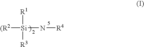
- A batch of wafer substrates is provided with each wafer substrate having a surface. Each surface is coated with a layer of material applied simultaneously to the surface of each of the batch of wafer substrates. The layer of material is applied to a thickness that varies less than four thickness percent across the surface and exclusive of an edge boundary and having a wafer-to-wafer thickness variation of less than three percent. The layer of material so applied is a silicon oxide, silicon nitride or silicon oxynitride with the layer of material being devoid of carbon and chlorine. The material deposition occurs ideally below 600° C. A silicon nitride layer of material is formed from a precursor having the Formula I or II alone or in combination with a coreactant:

where R1, R2 and R3 are each independently hydrogen or C1-8 alkyl, R1 is SiH3 when R2 and R3 are both hydrogen, and R4 is hydrogen, C1-8 alkyl, or Si bonded to R1, R2 and R3. Formation of silicon oxide or a silicon oxynitride requires the inclusion of a co-reactant. Silicon nitride is also formed with the inclusion of a nitrification co-reactant. - A process for forming such a batch of wafer substrates involves feeding the precursor into a reactor containing a batch of wafer substrates and reacting the precursor at a wafer substrate temperature, total pressure, and precursor flow rate sufficient to create such a layer of material. The delivery of a precursor and co-reactant as needed, through vertical tube injectors having multiple orifices with at least one orifice in registry with each of the batch of wafer substrates and exit slits within the reactor creates flow across the surface of each of the wafer substrates in the batch to yield the aforementioned within-wafer and wafer-to-wafer uniformity.
-
FIG. 1 is a cross-sectional view of a thermal processing apparatus having an across-flow injector system according to an embodiment of the present invention; -
FIG. 2 is a cross-sectional side view of a portion of the thermal processing apparatus ofFIG. 1 showing positions of injector orifices in relation to the liner and of exhaust slots in relation to the wafers according to an embodiment of the present invention; -
FIG. 3 is a plan view of a portion of the thermal processing apparatus ofFIG. 1 taken along the line A-A ofFIG. 1 inclusive of a stepped liner accommodating tube injectors and showing gas flow from injector orifices across a wafer and to an exhaust port; -
FIG. 4 is a perspective downward view of an across-flow stepped liner showing a longitudinal bulging section according to one embodiment of the present invention; -
FIG. 5 is a perspective downward view of an across-flow stepped liner showing a plurality of exhaust slots in the liner according to one embodiment of the present invention; -
FIG. 6 is a side view of an across-flow liner ofFIGS. 4 and 5 ; -
FIG. 7 is a top plan view of an across-flow liner depicted inFIGS. 4-6 ; -
FIG. 8 is a magnified top plan view of the bulging portion of across-flow liner depicted inFIG. 7 ; -
FIG. 9 is a perspective view of an across-flow injection system; -
FIG. 10 is a perspective view of another embodiment of an across-flow injection system; -
FIG. 11 is a plan view of an across-flow liner with a bulging section showing gas flow from orifices directing to the center of a wafer and exiting an exhaust slot according to one embodiment of the present invention; -
FIG. 12 is a plan view of an across-flow liner with a bulging section showing gas flow from orifices that impinges the liner inner wall prior to flowing across a wafer and exiting an exhaust slot according to one embodiment of the present invention; -
FIG. 13 is a plan view of an across-flow liner with a bulging section showing gas flow from orifices that impinges on each other and the liner inner wall prior to flowing across a wafer and exiting an exhaust slot according to one embodiment of the present invention; -
FIG. 14 is a graphical representation showing gas flow lines across the surface of a wafer inside a chamber including an across-flow liner and two injection tubes having injection orifices facing the liner inner wall according to one embodiment of the present invention; -
FIG. 15 is a graphical representation showing gas flow lines across the surface of a wafer inside a chamber including a prior art liner and two injection tubes having injection orifices facing the liner inner wall; -
FIG. 16 is a graphical representation showing gas flow lines across the surface of a wafer inside a chamber including an across-flow liner and two injection tubes having injection orifices facing each other according to one embodiment of the present invention; -
FIG. 17 is a graphical representation showing gas flow lines across the surface of a wafer inside a chamber including a prior art liner and two injection tubes having injection orifices facing each other; -
FIG. 18 is a graphical representation showing gas flow lines across the surface of a wafer inside a chamber including an across-flow liner and two injection tubes having injection orifices facing the center of a wafer according to one embodiment of the present invention; -
FIG. 19 is a graphical representation showing gas flow lines across the surface of a wafer inside a chamber including a prior art liner and two injection tubes having injection orifices facing to the center of a wafer; -
FIG. 20 is computational flow dynamics (CFD) demonstration for a thermal processing apparatus including an across-flow liner and an injection system having injection ports facing the liner inner wall in accordance with one embodiment of the present invention; -
FIG. 21 is CFD demonstration for a thermal processing apparatus including an across-flow liner and an injection system having injection ports facing each other in accordance with one embodiment of the present invention; -
FIG. 22 is CFD demonstration for a thermal processing apparatus including an across-flow liner and an injection system having injection ports facing the center of a substrate in accordance with one embodiment of the present invention; -
FIG. 23 is a CFD demonstration of the atomic oxygen concentration across the load for a conventional “up-flow” configuration reactor lacking a liner ofFIGS. 11-13 ; -
FIG. 24 is a CFD demonstration of the atomic oxygen concentration across the load for a across-flow configuration; -
FIG. 25 is an exemplary gas flow schematic for a two injector reactor ofFIG. 1 . -
FIG. 26 is a graph depicting low-T oxide material layer deposition and within-wafer (WIW) to one sigma as a function of deposition temperature. - The present invention has utility as a batch of semiconductor wafer substrates having deposited thereon a layer of a silicon nitride material, silicon oxide material, or silicon oxynitride material, the material layer exhibiting within-wafer uniformity of less than four thickness percent three sigma and a wafer-to-wafer uniformity of less than three thickness percent that are simultaneously produced absent carbon and chloride contamination. A process to achieve such a batch of wafer substrates is provided utilizing across-flow dispersion of reactants relative to a wafer substrate surface.
- As used herein within-wafer (WIW) variation is defined as the topological thickness variation across a 300 mm planar wafer substrate between the thinnest and thickest material layer deposited exclusive of an edge zone of 3 mm edge exclusion and shadow regions associated with a wafer carrier boat rail.
- As used herein, wafer-to-wafer (WTW) variation is defined as the maximal difference in average thickness in a material layer between a batch of multiple wafers simultaneously processed for layer deposition.
- A silicon-nitrogen-silicon (Si—N—Si) structure containing precursor is used to produce an inventive layer of a material simultaneously to a batch of wafer substrates. Preferably, the precursor is stable under an inert atmosphere at 20° C. An inventive precursor in acyclic form has the general formula:

Preferably, when the precursor has the structure according to Formula I, R1, R2 and R3 in every occurrence are identical. More preferably, R1, R2 and R3 are all hydrogen. Most preferably, R4 is the silicon bonded to R1, R2 and R3 where R1, R2 and R3 are all hydrogen and Formula (I) corresponds to trisilylamine (TSA). - A silicon-nitrogen-silicon structure containing cyclic precursor has the structure:

- where R1, R2 and R4 have the identities as detailed above with respect to the acyclic precursor of Formula I. Preferably, R1 and R2 in every occurrence are identical and R4 in every occurrence is identical. More preferably, R1 in every occurrence is hydrogen, R2 in every occurrence is hydrogen, and R4 is hydrogen or SiH3. It is noted that the inventive precursors of Formulas (I) and (II) are devoid of halogen moieties specifically exclusive of chlorine, and as a result the resulting layer of material deposited is independent of chlorine contaminants and chlorine/chloride containing volatile byproducts. A layer of material is deposited according to the present invention that is substantially devoid of carbon inclusion even though the precursor of Formula I or II includes alkyl moieties. However, the avoidance of carbon infiltrates into a deposited inventive layer of material typically requires that deposition rates be adjusted to under 10 Angstroms per minute. The deposition of inventive material layers devoid of carbon was readily accomplished through the selection of a precursor containing only silicon, nitrogen and hydrogen atoms.
- Mixtures of multiple precursors as detailed above are appreciated to be operative herein as well as the use of an inventive precursor with traditional silicon containing precursor compounds. Additionally, it is recognized that inventive precursor compounds may contain minor amounts of impurities that may be incorporated into an inventive material layer. Such impurity incorporation is diminished to acceptable levels through additional precursor purification prior to usage and storage under nonreactive conditions. Additionally, it is appreciated that an inventive precursor is stored with an inert diluent or metered through a reaction chamber with such a diluent with conventional techniques such as the employ of a mass flow controller (MFC).
- Formation of a layer SiyN where y is between 0.75 and 1 is noted to readily occur upon injecting a precursor into a reaction chamber with the wafer batch typically held at a temperature range of between 450° C. and 800° C. In instances where y is less than 1 and the precursor of Formula I or II is devoid of alkyl moieties, y-1 corresponds to the amount of hydrogen intercalation into the resultant silicon nitride material layer.
- It is appreciated that annealing a hydrogen containing silicon nitride material layer in the presence of a nitrogen source such as ammonia subsequent to deposition removes hydrogen from the layer and increases the nitrogen content of the resulting layer to the point where nitrogen-rich silicon nitride (Si3N4) is achieved. While the hydrogen depleting annealing can occur at temperatures above 400° C., the kinetics of such anneal increase with temperature. In instarices where thermal budget of a wafer substrate is an issue, rapid thermal processing and other flash annealing techniques are appreciated to be operative.
- In addition to pyrolysis of a precursor of Formula I or II, the deposition mechanism and/or film composition is altered by reacting a precursor of Formulas (I) and (II) with a nitrifying or oxidizing co-reactant. Such co-reactants illustratively include NH3, HN3, H2N2, secondary amines, tertiary amines, NH* radicals, NH2*radicals, O2, O3, O* radicals, OH* radicals, H2O, H2O2, NO, N2O, and NO2. Preferably, the co-reactant is devoid of carbon atoms and chlorine atoms. The co-reactant, if present, is injected into a reaction chamber either in concert with the precursor of Formula I or II, in an alternating pulsatile flow relative to the precursor, or after deposition of a material layer from the precursor has occurred. Post deposition introduction of the coreactant results in a post-processing modification. In instances where one desires to deposit a layer of silicon dioxide, preferably an oxygen containing co-reactant such as oxygen, ozone, water or a combination thereof is injected into the reactor volume in concert with the precursor of Formula I or II. Likewise, a layer of a material having a stoichiometry with little variation through the thickness of the layer is produced by injecting nitrogen and oxygen containing co-reactants into the reactor with the precursor of Formula I or II. Silicon oxynitride precursors include NOx molecules; a combination of an oxidizing precursor and a nitrifying precursor, such as ammonia; or combinations thereof. Production of a batch of wafer substrates containing a layer of material applied simultaneously thereto according to the present invention typically occurs at a pressure of less than 50 Torr and preferably less than 10 Torr. More preferably, the reactor pressure is maintained between 100 millitorr and 7 Torr total pressure through resort to an inert diluent gas to deposit a material layer. Inert diluent gases illustratively include the noble gases, dinitrogen or combinations thereof. It is appreciated that deposition rates of a layer of material vary considerably based not only on the material being deposited but also on flow rates, total reaction pressure, and temperature. One of skill in the art will appreciate that deposition rates of the deposition of all the inventive materials tend to increase with increases in temperature, precursor flow rate, and total pressure. The nature of such parameters will be further detailed with respect to the following examples.
- The deposition of various material layers according to the present invention and the conditions under which such deposition occurs where the precursor of Formula I or II is supplied at a flow rate of between 1 and 50 sccm is detailed in Table 1 where the units for the coreactant flow rate and inert diluent flow rate are in multiples of precursor flow rate.
TABLE 1 Typical Layer Deposition Conditions Coreactant Flow Rate Optional Inert Diluent (multiple of (multiple of Deposition Material precursor flow rate) precursor flow rate) Temp. (° C.) SiyN e.g. NH3 0-80x 10-200x 480-600 SiOx e.g. O2 5-100x 10-200x 200-600 SiOmNn e.g. N2O 3-100x 10-200x 480-600 - It is appreciated that a number of co-reactants detailed herein are in equilibrium with radical species. Without intending to be bound to a particular mechanistic theory, such radical species are believed to be involved in material layer deposition at the comparatively low temperatures of the present invention as compared to the prior art. The singlet oxygen (O*) formation from ozone and NO* formation from N2O are exemplary of known radical species formed under the temperature and pressure conditions detailed in Table 1. Optionally, radical species concentration generation is enhanced through the inclusion of the radical generator with which a precursor of Formula I or II, a co-reactant, or a combination thereof is exposed in the course of the material layer deposition process. Conventional radical generating sources operable within the context of the present invention include plasma discharge electrodes, photolysis sources, and rapid thermal in-situ steam generation (ISSG) processing. One of ordinary skill in the art will appreciate that while radical species concentration increase associated with the addition of a free radical generator tends to decrease the required deposition temperature, care is required to maintain reaction condition uniformity across a wafer surface and throughout a wafer batch reactor volume.
- A reactor well suited to yield material layer deposition in a batch process such that a batch of wafer substrates each receive a layer of material on a deposition surface simultaneously to a thickness of greater than 15 Angstroms such that the thickness of the material layer applied to each wafer surface varies less than four percent three sigma WIW and less than three percent in layer thickness WTW. Such a reactor overcomes problems associated with uniform precursor distribution within a batch chamber and utilizes elongated injector tubes rotatable about a tube axis with the injector tubes including orifices in registry with wafer carrier positions and a series of exit slits so as to create a flow across the multiple wafer surfaces of a batch in a laminar across flow pattern. Such a reactor is disclosed in WO 2005/031233 filed Sep. 22, 2004. Such a reactor is currently commercially available from Aviza Technology (Scotts Valley, Calif.).
- As shown in
FIG. 1 ,improved injectors 116 are used in thethermal processing apparatus 100. Theinjectors 116 are distributive or across-flow injectors 116-1 in which process gas or vapor is introduced through injector openings ororifices 180 on one side of thewafers 108 held inboat 106 and caused to flow across the surfaces of thewafers 108 in a laminar flow to exhaust ports orslots 182. Theexhaust slots 182 are aligned 180 degrees from theinjector system 116. In the alternative, theexhaust slots 182 are aligned at some other angle from theinjectors 116. The across-flow injector system 116 improves wafer uniformity within a batch ofwafers 108 by providing an improved distribution of process gas or vapor over earlier gas flow configurations. - Additionally, across-
flow injectors 116 can serve other purposes, including the injection of diluent gases between thewafers 108. Use of across-flow injectors 116 results in a more uniform cooling betweenwafers 108 whether a wafer substrate is disposed at the bottom, top or middle of the stack of wafers, as compared with earlier gas flow configurations. Preferably, theinjector 116orifices 180 are sized, shaped and positioned to provide a spray pattern that promotes forced convective cooling between thewafers 108 in a manner that does not create a large temperature gradient across the wafer. -
FIG. 1 is a cross-sectional view of an embodiment of a thermal processing apparatus for thermally processing a batch of semiconductor wafers. As shown, thethermal processing apparatus 100 generally includes avessel 101 that encloses a volume to form aprocess chamber 102 having asupport 104 adapted for receiving a carrier orboat 106 with a batch ofwafers 108 held therein, and heat source orfurnace 110 having a number of heating elements 112-1, 112-2 and 112-3 (referred to collectively hereinafter as heating elements 112) for raising a temperature of the wafers to the desired temperature for thermal processing. Thethermal processing apparatus 100 further includes one or more optical or electrical temperature sensing elements, such as a resistance temperature device (RTD) or thermocouple (T/C), for monitoring the temperature within theprocess chamber 102 and controlling operation of the heating elements 112. In the embodiment shown inFIG. 1 , the temperature sensing element is a profile T/C 114 that has multiple independent temperature sensing nodes or points (not shown) for detecting the temperature at multiple locations within theprocess chamber 102. Thethermal processing apparatus 100 can also include one ormore injectors 116, one of which 116-1 for introducing a fluid, such as a gas or vapor, into theprocess chamber 102 for processing or cooling thewafers 108, and one or more purge ports or vents 118 (only one of which is shown) for introducing a gas to purge the process chamber and cool the wafers. Aliner 120 increases the concentration of processing gas or vapor near thewafers 108 in a process zone 128 in which the wafers are processed, and reduces contamination of the wafers from flaking or peeling of deposits that can form on interior surfaces of theprocess chamber 102. Processing gas or vapor exits the process zone through exhaust ports or slots 121 in thechamber liner 120. - Generally, the
vessel 101 is sealed by a seal, such as an O-ring 122, to a platform orbase plate 124 to form theprocess chamber 102, which completely encloses thewafers 108 during thermal processing. The dimensions of theprocess chamber 102 and thebase plate 124 are selected to provide a rapid evacuation, rapid heating and a rapid backfilling of the process chamber. Advantageously, thevessel 101 and thebase plate 124 are sized to provide aprocess chamber 102 having dimensions selected to enclose a volume substantially no larger than necessary to accommodate theliner 120 with thecarrier 106 andwafers 108 held therein. Preferably, thevessel 101 and thebase plate 124 are sized to provide aprocess chamber 102 having dimensions of from about 125% to about 150% of that necessary to accommodate theliner 120 with thecarrier 106 andwafers 108 held therein, and more preferably, the process chamber has dimensions no larger than about 125% of that necessary to accommodate theliner 120 and thecarrier 106 andwafers 108 in order to minimize the chamber volume and thereby reduce pump down and backfill time required. - Openings for the
injectors 116, T/Cs 114 andvents 118 are sealed using seals such as o-rings, VCR®, or CF® fittings. Gases or vapor released or introduced during processing are evacuated through a foreline orexhaust port 126 formed in a wall of the process chamber 102 (not shown) or in aplenum 127 of thebase plate 124, as shown inFIG. 1 . Theprocess chamber 102 can be maintained at atmospheric pressure during thermal processing or evacuated to a vacuum as low as 5 milliTorr through a pumping system (not shown) including one or more roughing pumps, blowers, hi-vacuum pumps, and roughing, throttle and foreline valves. In the alternative, the process chamber can be evacuated to a vacuum lower than 5 milliTorr. - In another embodiment, shown in
FIG. 2 , thebase plate 124 further includes a substantially annular flow channel 129 adapted to receive and support aninjector 116 including a ring 131 from which depend a number of vertical injector tube or injectors 116-1. The injectors 116-1 can be sized and shaped to provide an up-flow, down-flow or across-flow flow pattern, as described below. The ring 131 and injectors 116-1 are located so as to inject the gas into theprocess chamber 102 between theboat 106 and thevessel 101. - The
vessel 101 andliner 254 can be made of any metal, ceramic, crystalline or glass material that is capable of withstanding the thermal and mechanical stresses of high temperature and high vacuum operation, and which is resistant to erosion from gases and vapors used or released during processing. Preferably, thevessel 101 andliner 120 are made from an opaque, translucent or transparent quartz glass having a sufficient thickness to withstand the mechanical stresses of the thermal processing operation and resist deposition of process byproducts. By resisting deposition of process byproducts, thevessel 101 andliner 254 reduce the potential for contamination of the processing environment. More preferably, thevessel 101 andliner 254 are made from quartz that reduces or eliminates the conduction of heat away from the process zone in which thewafers 108 are processed. - The
thermal processing apparatus 100 further includes a magnetically coupledwafer rotation system 162 that rotates thesupport 104 and theboat 106 along with thewafers 108 supported thereon during processing. In the alternative, thethermal apparatus 100 uses a rotational ferrofluidics seal (not shown) to rotate thesupport 104 and theboat 106 along with thewafers 108 supported thereon during processing. Rotating thewafers 108 during processing improves within-wafer (WIW) uniformity by averaging out any nonuniformities in temperature and process gas flow to create a uniform wafer temperature and species reaction profile. Generally, thewafer rotation system 162 is capable of rotating thewafers 108 at a speed of from about 0.1 to about 10 revolutions per minute (RPM). - The
wafer rotation system 162 includes a drive assembly orrotating mechanism 164 having arotating motor 166, such as an electric or pneumatic motor, and amagnet 168 encased in a chemically resistive container, such as annealed polytetrafluoroethylene or stainless steel. Asteel ring 170 located just below the insulatingblock 140 of the pedestal 130, and a drive shaft 172 with the insulating block transfer the rotational energy to anothermagnet 174 located above the insulating block in a top portion of the pedestal. Thesteel ring 170, drive shaft 172 andsecond magnet 174 are also encased in a chemically resistive container compound. Themagnet 174 located inside of the pedestal 130 magnetically couples through thecrucible 142 with a steel ring ormagnet 176 embedded in or affixed to thesupport 104 in theprocess chamber 102. - Magnetically coupling the
rotating mechanism 164 through the pedestal 130 eliminates the need for locating therotating mechanism 164 within the processing environment or for having a mechanical feedthrough, thereby eliminating a potential source of leaks and contamination. Furthermore, locatingrotating mechanism 164 outside and at some distance from theprocess chamber 102 minimizes the maximum temperature to which it is exposed, thereby increasing the reliability and operating life of thewafer rotation system 162. - In addition to the above, the
wafer rotation system 162 can further include one or more sensors (not shown) to ensureproper boat 106 position and proper magnetic coupling between the steel ring ormagnet 176 in theprocess chamber 102 and themagnet 174 in the pedestal 130. A boat position verification sensor which determines the relative position of theboat 106 is particularly useful. In one embodiment, the boat position verification sensor includes a sensor protrusion (not shown) on theboat 106 and an optical or laser sensor located below thebase plate 124. In operation, after thewafers 108 have been processed the pedestal 130 is lowered about 3 inches below thebase plate 124. There, thewafer rotation system 162 is commanded to turn theboat 106 until the boat sensor protrusion can be seen. Then, thewafer rotation system 162 is operated to align the boat so that thewafers 108 can be unloaded. After this is done, the boat is lowered to the load/unload height. -
FIG. 2 is a cross-sectional side view of a portion of thethermal processing apparatus 100 ofFIG. 1 showing illustrative portions of theinjector orifices 180 in relation to theliner 120 and theexhaust slots 182 in relation to thewafers 108, where like numerals correspond to those detailed with respect toFIG. 1 . -
FIG. 3 shows athermal processing apparatus 230 including an across-flow liner 232 operative with the present invention. To simplify description of the invention, elements not closely relevant to the invention are not indicated in the drawing or described. In general, theapparatus 230 includes avessel 101 that forms aprocess chamber 102 having asupport 104 adapted for receiving acarrier 106 with a batch ofwafers 108 held therein. Theapparatus 230 includes a heat source or furnace 112-2 that heats thewafers 108 to the desired temperature for thermal processing. An across-flow liner 232 is provided to increase the concentration of processing gas or vapor nearwafers 108 and reduce contamination ofwafers 108 from flaking or peeling of deposits that can form on interior surfaces of thevessel 101. Theliner 232 is patterned to conform to the contour of thewafer carrier 106 and sized to reduce the gap between thewafer carrier 106 and theliner 232. Theliner 232 is mounted to thebase plate 124 and sealed. - Stepped liners are typically used in traditional up-flow vertical furnaces to increase process gas velocities and diffusion control. They are also used as an aid to improve within-wafer uniformity. Unfortunately, stepped liners do not correct down-the-stack-depletion problems, which occur due to single injection point of reactant gases forcing all injected gases to flow past all surfaces down the stack. In prior art vertical across-flow furnaces, the down-the-stack-depletion problem is solved. However, a flow path of least resistance may be created in the gap region between the wafer carrier and the liner inner wall instead of between the wafers. This least resistance path may cause vortices or stagnation which are detrimental to manufacturing processes. Vortices and stagnation in a furnace may create across-wafer nonuniformity problems for some process chemistries.
- The present invention provides an across-flow liner that significantly improves the within-wafer uniformity by providing uniform gas flow across the surface of each substrate supported in a carrier. In general, the across-flow liner of the present invention includes a longitudinal bulging section to accommodate an across-flow injection system so that the liner can be patterned and sized to conform to the wafer carrier. The gap between the liner and the wafer carrier is significantly reduced, and as a result, vortices and stagnation as occurred in prior art furnaces can be reduced or avoided.
- Referring to
FIGS. 4-8 , an across-flow injection system 116 is disposed within a long-bulgingsection 262 of theliner 232. Gases are introduced through a plurality ofinjection port orifices 252 from one side of thewafers 108 andcarrier 106 and flow across the surface of the wafers in a laminar flow as described below. A plurality ofslots 254 are formed in theliner 232 in a location approximately 180 degrees from the long-bulgingsection 262. The size and pattern of theslots 254 are predetermined and preferably cooperate with the spacing between and number of theinjection orifices - The across-flow liner can be made of any metal, ceramic, crystalline or glass material that is capable of withstanding the thermal and mechanical stresses of high temperature and high vacuum operation, and which is resistant to erosion from gases and vapors used or released during processing. Preferably, the across-
flow liner 232 is made from an opaque, translucent or transparent quartz glass. In one embodiment, the liner is made from quartz that reduces or eliminates the conduction of heat away from the region or process zone in which the wafers are processed. - In general, the across-
flow liner 232 includes acylinder 256 having aclosed end 258 and anopen end 260. Thecylinder 256 is provided with the longitudinal bulgingsection 262 having aninner wall 270 to accommodate an across-flow injection system (not shown). Preferably the bulgingsection 262 extends the substantial length of thecylinder 256. The plurality oflatitudinal slots 254 are radial in their length and longitudinally located along thecylinder 256. - The across-
flow liner 232 is sized and patterned to conform to the contour of thewafer carrier 106 and thecarrier support 104. In one embodiment, theliner 232 comprises afirst section 261 sized to conform to thewafer carrier 100 and asecond section 263 sized to conform to thecarrier support 104. The diameter of thefirst section 261 may differ from the diameter of thesecond section 263, i.e., theliner 232 may be “stepped” to conform to thewafer carrier 106 andcarrier support 104 respectively. In one embodiment, thefirst section 261 of theliner 232 has an inner diameter that constitutes about 104% to 110% of thewafer carrier 106 outer diameter. In another embodiment, thesecond section 263 of theliner 232 has an inner diameter that constitutes about 115% to 120% of the outer diameter of thecarrier support 104. Thesecond section 263 may be provided with one ormore heat shields 264 to protect seals such as O-rings from being overheated by heating elements. -
FIG. 6 is a side view of the across-flow liner 232. The longitudinal bulgingsection 262 extends the length of thefirst section 261. The injection system 250 (not shown) is accommodated in the bulgingsection 262 and introduces one or more gases into the across-flow liner 232 between thewafers 242. One ormore heat shields 264 can be provided in thesecond section 263. -
FIG. 7 is a top plan view of the across-flow liner 232 showing theclosed end 258 of thecylinder 256 havingopenings 266 for receiving the across-flow injection system 250. Theinjection system 250 has at least one injection tube 251 (described in detail below) to fit within theopenings 266. As shown in detail inFIG. 8 , theopenings 266 in theclosed end 258 havenotches 268 for orienting and stabilizing an across-flow injection system. Although three notches (268A, 268B, 268C) are shown in theopenings 266 for illustrative purpose, it should be noted that any number of notches can be formed so that the injection tube can be oriented to any direction relative to the across-flow liner 232 and to each other. - Referring to
FIG. 9 , the across-flow injection system 250 comprises one or more elongated tubes 251 rotatable about an axis perpendicular to the desired processing surfaces of thewafers 242. In the preferred embodiment, the elongated tubes 251 are provided with a plurality of injection ports ororifices 252 longitudinally distributed along the length of the tubes for directing reactant and other gases across the surface of each substrate. Theinjection port orifices 180 have the same area or in the alternative, theinjection port orifices 252 can vary in area along the length of the injector tube 251, as depicted inFIG. 10 . In addition, the inner diameter of two or more elongated tube injectors 116-1 and 116-2 are equal (FIG. 9 ), or in the alternative the inner diameter of two or more tube injectors 251 -1 and 251-2 can be different (FIG. 10 ). The injection orifices 180 or 252 are preferably equally spaced along the length of theinjection tube 116 or 251, and in registry withslots boat 106. - In one embodiment, the
elongated tubes 116 or 251 include anindex pin 253 for locking the elongated tube in one of thenotches 268 in theopenings 266, and the injection ports ororifices 252 are formed in line with the index pin. Therefore, when the elongated tube is installed, theindex pin 253 can be locked in one of thenotches 268 and theinjection orifices appropriate notch 268. An indicator (not shown) located on the opposite end of tubes 251 further allows a user to adjust the location of theinjection ports 252. This adjustment is performed before, during and after a thermal processing run without removal of the across-flow liner 232 from thevessel 234. - Of advantage, the bulging
section 262 of the across-flow liner 232 accommodates the across-flow injection system liner 232 is made conformal to the contour of thewafer carrier 106. This confirming of theliner 232 to thewafer carrier 106 reduces the gap between the liner and the wafer carrier, thereby reducing the vortices and stagnation in the gap regions between the liner inner wall and thewafer carrier 106, improving gas flow uniformity and the quality, uniformity, and repeatability of the deposited film. - The
base plate 124 has anopening 266 to receive the tube injectors.Notches 268 are formed in thebase plate 124 to orient the injection ports 116-1, 116-2, 251-2 or 252-2 to a specific direction. Any number ofnotches 268 can be formed so that the elongated injection tubes can be adjusted 360 degrees relative to a fixed position and theinjection ports 252 can be oriented in any direction as desired. For example, theindex pin 253 the elongated tube injector 251-2 can be received innotch 268A so that theinjection ports 252′ are oriented to face wafer substrates and the exit slots. As indicated inFIG. 11 , gases exiting theinjection ports liner wall 270 of the bulgingsection 262 prior to flowing across the surface of eachsubstrate 108 to theexit slot 244. Alternatively, the index pins 253 in the elongated tube injectors 116-1/116-2 or 252-1/252-2 are received in notches so that theinjection orifices FIGS. 12-13 , gases exiting theinjection orifices wafer 108. -
FIGS. 14-19 are “particle trace” graphics representing gas flow lines across the surface of a substrate inside a chamber. The graphics show particle traces 272 from injector orifices to an exhaust slot under various flow conditions. The flow momentum out of the first (leftmost) injector orifice is ten times greater than the second (rightmost) injector port. The across-flow liner ofFIGS. 14, 16 and 18 and the rotation of injectors both provide advantages in providing uniform gas flows across the surface of a substrate as compared to existing gas delivery systems. The bulgingsection 262 in the across-flow liner 234 provides a mixing chamber for the gases exiting the injection ports prior to flowing across the surface of a substrate and thus facilitate momentum transfer of “ballistic mixing” of gases. In contrast, in the chamber with or without a bulging section, the gas flow across the surface of a substrate is less regular, as shown inFIGS. 15, 17 and 19 for a given rotational orientation of injectors. - In operation, a vacuum system produces a vacuum pressure in the
reaction chamber 102. The vacuum pressure acts in the vertical direction of thevessel 101. The across-flow liner 232 is operative in response to the vacuum pressure to create a second vacuum inside the across-flow liner 232. The second vacuum pressure acts in a horizontal direction and across the surface of eachsubstrate 108. Two gases, for example a first gas and a second gas, are introduced into the two elongated tubes 251 of theinjection system injection ports 252 on one side of thewafer 108 and pass as laminar flow across thewafer 242 to theslots 254 and between twoadjacent wafers 108. Excessive gases or reaction byproducts are exhausted through thelatitudinal slots 254 in theliner wall 232 cooperative with theinjection orifices -
FIGS. 20-22 are Computational Fluid Dynamics (CFD) demonstrations for a thermal processing apparatus including an across-flow liner according to one embodiment of the present invention. The across-flow liner has a reduced diameter and is conformal to the wafer carrier. An across-flow injection system is accommodated in a bulging section of the liner. The injection system includes two elongated injection tubes each having a plurality of injection orifices to introduce reactant or other gases across the surface of each substrate. The injection orifices are oriented to face the liner inner surface (FIG. 20 ) such that the gases exiting the injection ports impinge the liner wall and mix in the bulging section prior to flowing across the surface of each substrate; the wafer center (FIG. 21 ); and face each other so that the gases exiting the injection ports impinge each other and mix prior to flowing across the surface of each substrate (FIG. 22 ). The gases introduced into the two tube injectors are trisilylamine and NH3 respectively at 75 sccm. -
FIG. 23 is CFD demonstration for the concentration of atomic oxygen radicals as a result of introducing ozone into the injectors of a conventional up-flow furnace configuration lacking the injector and liner of the reactor depicted inFIG. 1 .Wafer number 1 is at the bottom of the stack and the flow of the oxygen radicals is from the bottom to the top. The demonstration shows poor atomic oxygen concentration uniformity across the wafers and across the stack of wafers, resulting in poor uniformity of the desired film formation. -
FIG. 24 is CFD demonstration for the concentration of atomic oxygen radicals as a result of introducing ozone into the injectors of an across-flow furnace configuration ofFIG. 1 .Wafer number 1 is at the bottom of the stack and the flow of the oxygen radicals is across flow. The demonstration shows very good atomic oxygen concentration uniformity WIN and WTW resulting in the desired film formation. - An exemplary gas flow schematic for a two injector reactor is depicted in
FIG. 25 . Aprecursor 50 is provided in fluid communication with injector 116-1 withinvessel 101 with reference toFIG. 1 . Aninert gas source 52 is optionally interconnected to injector 116-1. With the use of conventional valves a mass flow controller (MFC) bothsource vessel 101 by injector 116-1. With registry of awafer surface 104 and anexhaust slot 254 an across flow of reactants with a high degree of uniformity on a given wafer surface and vertically displaced wafers is achieved. In a similar manner, aco-reactant source 54 alone, aninert gas source 52′, or a combination thereof are selectively metered to injector 116-2. The co-reactant is optionally exposed to the discharge of aplasma generator 55 prior to contacting a wafer substrate. It is appreciated that with conventional gas connection schemes,inert gas sources 52′ is supplied byinert gas source 52. It is further appreciated that flowing inert gas through an injector when a reactant is not being provided through that injector tends to inhibit backflow into the unused injector. - The ability to deposit a layer of material on a wafer substrate batch with uniformity WIW and WTW of the batch is provided in additional detail in the following working examples. These exemplary, nonlimiting examples are intended to illustrate the conditions under which inventive deposition might occur.
- A batch of 20 wafers was dispersed along a 120 wafer carrier with substrate blanks filling the unused 100 positions. After stabilizing a wafer substrate temperature and an inert dinitrogen atmosphere, trisilylamine and ammonia gas are introduced into the reactor at flow rates of 15 and 225 sccm while the reactor total pressure is maintained at 3 Torr with a controlled flow of argon gas. The deposition is allowed to proceed for 30 minutes at a reaction temperature of 515° C. A deposition rate of 1.8 Angstroms per minute is noted. WIW uniformity for the resultant silicon nitride film is 2.3 thickness percent (three sigma) while WTW thickness variation is 2.6 percent. Auger spectroscopy indicated the resultant deposited layer of material to be devoid of carbon and chlorine and having less than 8 atomic percent substitution hydrogen for the silicon counterions.
- The process of Example 1 is repeated with a change in wafer substrate temperature. Comparable uniformity to that of Example 1 is noted while variations in deposition rate as a function of temperature are provided in Table 2 along with the comparative temperature and deposition rates for prior art precursors. Auger spectroscopy indicated the resultant deposited layer of material to be devoid of carbon and chlorine and having less than 10 atomic percent substitution hydrogen for the silicon counterions.
TABLE 2 Batch SiN Layer Deposition as a Function of Temperature Substrate Temp. Deposition Rate Example Precursor (° C.) (Å/mm) 1 trisilylamine/NH3 515 1.8 2 trisilylamine/NH3 525 4.0 3 trisilylamine/NH3 540 9.3 4 trisilylamine/NH3 550 10.3 5 trisilylamine/NH3 575 13 6 trisilylamine/NH3 600 18 Comp. A dichlorosilane/NH3 750 17.3 Comp. B bis t-butylamino 570 10.0 silane/NH3 - A low temperature oxide material layer is deposited with the reactor according to
FIG. 1 with the reactor maintained at a total pressure of 7 Torr with dinitrogen as an inert gas, trisilylamine and oxygen being metered into the reactor at rates of 11 and 200 sccm, respectively. The nitrogen flow rate is approximately 500 sccm. The deposition rate and WIW nonuniformity (one sigma) as a function of deposition temperature between 200°0 and 450° C. is provided inFIG. 6 . WTW variation is less than 3%. Auger spectroscopy indicated the resultant deposited layer of material to be devoid of carbon and chlorine and having less than 10 atomic percent substitution hydrogen for the silicon counterions. - A silicon oxynitride deposition layer is applied to a batch of wafer substrates with a total pressure of 2 Torr using dinitrogen as an inert gas, trisilylamine and N2O flowing at rates of 15 and 300 sccm, respectively. With the simultaneous flow of trisilylamine and N2O for a period of 30 minutes at a wafer substrate temperature of 525° C., silicon oxynitride deposition is noted to have occurred at a deposition rate of greater than 100 Angstroms per minute in a composition SiOmNn where m is reproducibly 0.77 and n is 0.33. WIW variation is less than 3% three sigma and WTW thickness variation is less than 2.8%. Auger spectroscopy indicated the resultant deposited layer of material to be devoid of carbon and chlorine and having less than 10 atomic percent substitution hydrogen for the silicon counterions. The resultant deposited layer of material is observed to have an index of refraction of between 1.7 and 1.9 for various batches.
- Patent documents and publications mentioned in the specification are indicative of the levels of those skilled in the art to which the invention pertains. These documents and publications are incorporated herein by reference to the same extent as if each individual document or publication was specifically and individually incorporated herein by reference.
- The foregoing description is illustrative of particular embodiments of the invention, but is not meant to be a limitation upon the practice thereof. The following claims, including all equivalents thereof, are intended to define the scope of the invention.
Claims (25)
1. A batch of wafer substrates, each wafer substrate of the batch of wafer substrates having a surface, said batch of wafer substrates comprising:
a layer of material applied simultaneously onto the surface of each of the batch of wafer substrates to a thickness that varies less than four thickness percent three sigma within each wafer substrate exclusive of an edge boundary and having a wafer-to-wafer thickness variation of less than three percent, said material selected from the group consisting of SiOx where x is between 1.9 and 2.0 inclusive, SiyN where y is between 0.75 and 1 inclusive, and SiOmNn where n/(n+m) is between 0.2 and 0.4 inclusive; said layer of material substantially devoid of carbon and chlorine.
2. The batch of wafer substrates of claim 1 wherein each wafer substrate has a diameter of 300 millimeters.
3. The batch of wafer substrates of claim 1 wherein said material is SiyN and hydrogen is present in an amount of equal to or less than 1-y when y is less than 1 and greater than 0.75.
4. The batch of wafers of claim 3 wherein the thickness varies less than three thickness percent within each wafer substrate.
5. The batch of wafers of claim 1 wherein said batch has from 2 to 200 substrates.
6. The batch of wafers of claim 1 wherein said material is SiOmNn and m is between 0.6 and 0.8 and n is between 0.2 and 0.4 inclusive.
7. A process of simultaneously depositing a layer of material onto a batch of wafer substrates comprising:
feeding a Si—N—Si structure containing precursor into a reactor containing said batch of wafer substrates; and
reacting said Si—N—Si structure containing precursor at a wafer substrate temperature, total pressure, and precursor flow rate to form a layer of material onto a surface of each said batch of wafer substrates to a thickness that varies less than four thickness percent three sigma within each wafer across the surface exclusive of an edge boundary and having a wafer-to-wafer thickness variation of less than three percent, said layer substantially devoid of carbon and chlorine.
8. The process of claim 7 wherein said Si—N—Si structure containing precursor is trisilylamine.
9. The process of claim 7 further comprising introducing a coreactant into said reactor, said coreactant modifying a material layer deposition factor selected from the group consisting of: deposition mechanism and material layer composition.
10. The process of claim 9 wherein said coreactant is a nitrification reactant.
11. The process of claim 10 wherein said nitrification reactant is selected from the group consisting of: NH3, HN3, H2N2, secondary amines, tertiary amines, NH* and NH2*; and said layer of material has the formula SiyN where y is between 0.75 and 1 inclusive.
12. The process of claim 9 wherein said co-reactant is an oxidation reactant.
13. The process of claim 12 wherein said oxidation reactant is selected from the group consisting of: O2, O3, O*, OH*, H2O, H2O2, NO, N2O, NO2, and combinations thereof.
14. The process of claim 12 wherein said layer of material is SiOx where x is between 1.9 and 2.0 inclusive.
15. The process of claim 8 wherein said wafer substrate temperature is less than 600° Celsius and said total pressure is less than 30 Torr.
16. The process of claim 9 wherein said wafer substrate temperature is less than 550° Celsius and said pressure is less than 10 Torr and said precursor and said coreactant are metered simultaneously into said reactor.
17. The process of claim 7 wherein said Si—N—Si structure containing precursor is fed into said reactor through a vertical tube injector having a plurality of orifices, at least one of said plurality of orifices in registry with each of said batch of wafer substrates and exit slits to create a flow across the surface of each of said batch of wafer substrates.
18. The process of claim 17 further comprising delivering a coreactant to said reactor through a second vertical tube injector having a second plurality of orifices, at least one of said secondary plurality of orifices in registry with each of said batch of wafer substrates and said exit slits.
19. The process of claim 18 wherein said precursor and said coreactant are simultaneously fed into said reactor.
20. The process of claim 18 wherein said coreactant includes oxygen atoms and nitrogen atoms to yield said layer of material having a composition SiOmNn where m is between 0.6 and 0.8 inclusive and n is between 0.2 and 0.4 inclusive.
21. The process of claim 18 wherein said coreactant is an oxidation reactant and said layer of material has a composition SiOx where x is between 1.9 and 2.0 inclusive.
22. The process of claim 18 wherein said coreactant is a nitrification reactant and said layer of material has a composition SiyN where y is between 0.75 and 1 inclusive.
23. The process of claim 18 wherein said coreactant is fed to said reactor at a rate of more than three times that of said precursor.
24. The process of claim 7 wherein said precursor has the formula:

where R1, R2 and R3 are each independently hydrogen or C1-8 alkyl, R1 is SiH3 when R2 and R3 are both hydrogen, and R4 is hydrogen, C1-8 alkyl, or Si bonded to R1, R2 and R3.
25. The process of claim 9 further comprising exposing said coreactant to a plasma generator discharge.
Priority Applications (5)
| Application Number | Priority Date | Filing Date | Title |
|---|---|---|---|
| US11/482,887 US20070010072A1 (en) | 2005-07-09 | 2006-07-07 | Uniform batch film deposition process and films so produced |
| EP06786667A EP1908098A2 (en) | 2005-07-09 | 2006-07-10 | Uniform batch film deposition process and films so produced |
| JP2008521474A JP2009500864A (en) | 2005-07-09 | 2006-07-10 | Uniform batch film deposition process and film produced accordingly |
| KR1020087002811A KR20080033965A (en) | 2005-07-09 | 2006-07-10 | Uniform batch film deposition process and films so produced |
| PCT/US2006/026588 WO2007008705A2 (en) | 2005-07-09 | 2006-07-10 | Uniform batch film deposition process and films so produced |
Applications Claiming Priority (2)
| Application Number | Priority Date | Filing Date | Title |
|---|---|---|---|
| US69778405P | 2005-07-09 | 2005-07-09 | |
| US11/482,887 US20070010072A1 (en) | 2005-07-09 | 2006-07-07 | Uniform batch film deposition process and films so produced |
Publications (1)
| Publication Number | Publication Date |
|---|---|
| US20070010072A1 true US20070010072A1 (en) | 2007-01-11 |
Family
ID=37618804
Family Applications (1)
| Application Number | Title | Priority Date | Filing Date |
|---|---|---|---|
| US11/482,887 Abandoned US20070010072A1 (en) | 2005-07-09 | 2006-07-07 | Uniform batch film deposition process and films so produced |
Country Status (5)
| Country | Link |
|---|---|
| US (1) | US20070010072A1 (en) |
| EP (1) | EP1908098A2 (en) |
| JP (1) | JP2009500864A (en) |
| KR (1) | KR20080033965A (en) |
| WO (1) | WO2007008705A2 (en) |
Cited By (374)
| Publication number | Priority date | Publication date | Assignee | Title |
|---|---|---|---|---|
| US20080075838A1 (en) * | 2006-09-22 | 2008-03-27 | Hisashi Inoue | Oxidation apparatus and method for semiconductor process |
| US20090159004A1 (en) * | 2007-12-20 | 2009-06-25 | Elpida Memory, Inc. | Vertical chemical vapor deposition apparatus having nozzle for spraying reaction gas toward wafers |
| US20090232985A1 (en) * | 2005-03-17 | 2009-09-17 | Christian Dussarrat | Method of forming silicon oxide containing films |
| WO2010010088A1 (en) * | 2008-07-23 | 2010-01-28 | Ionbond Ag Olten | Chemical vapor deposition reactor for depositing layers made of a reaction gas mixture onto workpieces |
| US20110034039A1 (en) * | 2009-08-06 | 2011-02-10 | Applied Materials, Inc. | Formation of silicon oxide using non-carbon flowable cvd processes |
| US20110129616A1 (en) * | 2009-12-02 | 2011-06-02 | Applied Materials, Inc. | Oxygen-doping for non-carbon radical-component cvd films |
| US20110159703A1 (en) * | 2009-12-30 | 2011-06-30 | Applied Materials, Inc. | Dielectric film growth with radicals produced using flexible nitrogen/hydrogen ratio |
| US20110159213A1 (en) * | 2009-12-30 | 2011-06-30 | Applied Materials, Inc. | Chemical vapor deposition improvements through radical-component modification |
| US20110217851A1 (en) * | 2010-03-05 | 2011-09-08 | Applied Materials, Inc. | Conformal layers by radical-component cvd |
| US20120070957A1 (en) * | 2010-09-20 | 2012-03-22 | Applied Materials, Inc. | Air gap formation |
| US8466073B2 (en) | 2011-06-03 | 2013-06-18 | Applied Materials, Inc. | Capping layer for reduced outgassing |
| CN103165497A (en) * | 2013-02-20 | 2013-06-19 | 上海华力微电子有限公司 | Oxidation reacting furnace and method utilizing the same to conduct oxidizing reaction |
| US8551891B2 (en) | 2011-10-04 | 2013-10-08 | Applied Materials, Inc. | Remote plasma burn-in |
| US20130327273A1 (en) * | 2009-02-27 | 2013-12-12 | Hitachi Kokusai Electric Inc. | Substrate processing apparatus |
| US8617989B2 (en) | 2011-09-26 | 2013-12-31 | Applied Materials, Inc. | Liner property improvement |
| US8664127B2 (en) | 2010-10-15 | 2014-03-04 | Applied Materials, Inc. | Two silicon-containing precursors for gapfill enhancing dielectric liner |
| US8716154B2 (en) | 2011-03-04 | 2014-05-06 | Applied Materials, Inc. | Reduced pattern loading using silicon oxide multi-layers |
| US20140264774A1 (en) * | 2013-03-13 | 2014-09-18 | Inotera Memories, Inc. | Wafer and film coating method of using the same |
| US8889566B2 (en) | 2012-09-11 | 2014-11-18 | Applied Materials, Inc. | Low cost flowable dielectric films |
| US20140346650A1 (en) * | 2009-08-14 | 2014-11-27 | Asm Ip Holding B.V. | Systems and methods for thin-film deposition of metal oxides using excited nitrogen-oxygen species |
| US8921235B2 (en) | 2013-03-04 | 2014-12-30 | Applied Materials, Inc. | Controlled air gap formation |
| WO2015047914A1 (en) * | 2013-09-27 | 2015-04-02 | Antonio Sanchez | Amine substituted trisilylamine and tridisilylamine compounds |
| US9005539B2 (en) | 2011-11-23 | 2015-04-14 | Asm Ip Holding B.V. | Chamber sealing member |
| US9017481B1 (en) | 2011-10-28 | 2015-04-28 | Asm America, Inc. | Process feed management for semiconductor substrate processing |
| US9018108B2 (en) | 2013-01-25 | 2015-04-28 | Applied Materials, Inc. | Low shrinkage dielectric films |
| US9018111B2 (en) | 2013-07-22 | 2015-04-28 | Asm Ip Holding B.V. | Semiconductor reaction chamber with plasma capabilities |
| US9021985B2 (en) | 2012-09-12 | 2015-05-05 | Asm Ip Holdings B.V. | Process gas management for an inductively-coupled plasma deposition reactor |
| US9029253B2 (en) | 2012-05-02 | 2015-05-12 | Asm Ip Holding B.V. | Phase-stabilized thin films, structures and devices including the thin films, and methods of forming same |
| US20150144622A1 (en) * | 2013-11-27 | 2015-05-28 | Tokyo Electron Limited | Microwave heat treatment apparatus and microwave heat treatment method |
| US9096931B2 (en) | 2011-10-27 | 2015-08-04 | Asm America, Inc | Deposition valve assembly and method of heating the same |
| US9117866B2 (en) | 2012-07-31 | 2015-08-25 | Asm Ip Holding B.V. | Apparatus and method for calculating a wafer position in a processing chamber under process conditions |
| US9167625B2 (en) | 2011-11-23 | 2015-10-20 | Asm Ip Holding B.V. | Radiation shielding for a substrate holder |
| US9169975B2 (en) | 2012-08-28 | 2015-10-27 | Asm Ip Holding B.V. | Systems and methods for mass flow controller verification |
| US9177784B2 (en) | 2012-05-07 | 2015-11-03 | Asm Ip Holdings B.V. | Semiconductor device dielectric interface layer |
| US9202727B2 (en) | 2012-03-02 | 2015-12-01 | ASM IP Holding | Susceptor heater shim |
| US9228259B2 (en) | 2013-02-01 | 2016-01-05 | Asm Ip Holding B.V. | Method for treatment of deposition reactor |
| US9240412B2 (en) | 2013-09-27 | 2016-01-19 | Asm Ip Holding B.V. | Semiconductor structure and device and methods of forming same using selective epitaxial process |
| US9285168B2 (en) | 2010-10-05 | 2016-03-15 | Applied Materials, Inc. | Module for ozone cure and post-cure moisture treatment |
| US9299595B2 (en) | 2012-06-27 | 2016-03-29 | Asm Ip Holding B.V. | Susceptor heater and method of heating a substrate |
| US9324811B2 (en) | 2012-09-26 | 2016-04-26 | Asm Ip Holding B.V. | Structures and devices including a tensile-stressed silicon arsenic layer and methods of forming same |
| US9341296B2 (en) | 2011-10-27 | 2016-05-17 | Asm America, Inc. | Heater jacket for a fluid line |
| US20160148801A1 (en) * | 2014-11-25 | 2016-05-26 | Tokyo Electron Limited | Substrate processing apparatus, substrate processing method and storage medium |
| US9384987B2 (en) | 2012-04-04 | 2016-07-05 | Asm Ip Holding B.V. | Metal oxide protective layer for a semiconductor device |
| US9394608B2 (en) | 2009-04-06 | 2016-07-19 | Asm America, Inc. | Semiconductor processing reactor and components thereof |
| US9396934B2 (en) | 2013-08-14 | 2016-07-19 | Asm Ip Holding B.V. | Methods of forming films including germanium tin and structures and devices including the films |
| US9404178B2 (en) | 2011-07-15 | 2016-08-02 | Applied Materials, Inc. | Surface treatment and deposition for reduced outgassing |
| US9404587B2 (en) | 2014-04-24 | 2016-08-02 | ASM IP Holding B.V | Lockout tagout for semiconductor vacuum valve |
| US9412581B2 (en) | 2014-07-16 | 2016-08-09 | Applied Materials, Inc. | Low-K dielectric gapfill by flowable deposition |
| US9447498B2 (en) | 2014-03-18 | 2016-09-20 | Asm Ip Holding B.V. | Method for performing uniform processing in gas system-sharing multiple reaction chambers |
| US9455138B1 (en) | 2015-11-10 | 2016-09-27 | Asm Ip Holding B.V. | Method for forming dielectric film in trenches by PEALD using H-containing gas |
| US9478415B2 (en) | 2015-02-13 | 2016-10-25 | Asm Ip Holding B.V. | Method for forming film having low resistance and shallow junction depth |
| US9484191B2 (en) | 2013-03-08 | 2016-11-01 | Asm Ip Holding B.V. | Pulsed remote plasma method and system |
| US9493874B2 (en) * | 2012-11-15 | 2016-11-15 | Cypress Semiconductor Corporation | Distribution of gas over a semiconductor wafer in batch processing |
| US9543180B2 (en) | 2014-08-01 | 2017-01-10 | Asm Ip Holding B.V. | Apparatus and method for transporting wafers between wafer carrier and process tool under vacuum |
| US9558931B2 (en) | 2012-07-27 | 2017-01-31 | Asm Ip Holding B.V. | System and method for gas-phase sulfur passivation of a semiconductor surface |
| US9556516B2 (en) | 2013-10-09 | 2017-01-31 | ASM IP Holding B.V | Method for forming Ti-containing film by PEALD using TDMAT or TDEAT |
| US9589770B2 (en) | 2013-03-08 | 2017-03-07 | Asm Ip Holding B.V. | Method and systems for in-situ formation of intermediate reactive species |
| US9605343B2 (en) | 2013-11-13 | 2017-03-28 | Asm Ip Holding B.V. | Method for forming conformal carbon films, structures conformal carbon film, and system of forming same |
| US9607837B1 (en) | 2015-12-21 | 2017-03-28 | Asm Ip Holding B.V. | Method for forming silicon oxide cap layer for solid state diffusion process |
| US9627221B1 (en) | 2015-12-28 | 2017-04-18 | Asm Ip Holding B.V. | Continuous process incorporating atomic layer etching |
| US9640416B2 (en) | 2012-12-26 | 2017-05-02 | Asm Ip Holding B.V. | Single-and dual-chamber module-attachable wafer-handling chamber |
| US9647114B2 (en) | 2015-08-14 | 2017-05-09 | Asm Ip Holding B.V. | Methods of forming highly p-type doped germanium tin films and structures and devices including the films |
| US9659799B2 (en) | 2012-08-28 | 2017-05-23 | Asm Ip Holding B.V. | Systems and methods for dynamic semiconductor process scheduling |
| US9657845B2 (en) | 2014-10-07 | 2017-05-23 | Asm Ip Holding B.V. | Variable conductance gas distribution apparatus and method |
| US9711345B2 (en) | 2015-08-25 | 2017-07-18 | Asm Ip Holding B.V. | Method for forming aluminum nitride-based film by PEALD |
| US20170207078A1 (en) * | 2016-01-15 | 2017-07-20 | Taiwan Semiconductor Manufacturing Co., Ltd. | Atomic layer deposition apparatus and semiconductor process |
| US9735024B2 (en) | 2015-12-28 | 2017-08-15 | Asm Ip Holding B.V. | Method of atomic layer etching using functional group-containing fluorocarbon |
| US9754779B1 (en) | 2016-02-19 | 2017-09-05 | Asm Ip Holding B.V. | Method for forming silicon nitride film selectively on sidewalls or flat surfaces of trenches |
| US9777025B2 (en) | 2015-03-30 | 2017-10-03 | L'Air Liquide, Société pour l'Etude et l'Exploitation des Procédés Georges Claude | Si-containing film forming precursors and methods of using the same |
| US9793135B1 (en) | 2016-07-14 | 2017-10-17 | ASM IP Holding B.V | Method of cyclic dry etching using etchant film |
| US9790595B2 (en) | 2013-07-12 | 2017-10-17 | Asm Ip Holding B.V. | Method and system to reduce outgassing in a reaction chamber |
| US9793115B2 (en) | 2013-08-14 | 2017-10-17 | Asm Ip Holding B.V. | Structures and devices including germanium-tin films and methods of forming same |
| US9793148B2 (en) | 2011-06-22 | 2017-10-17 | Asm Japan K.K. | Method for positioning wafers in multiple wafer transport |
| US9812320B1 (en) | 2016-07-28 | 2017-11-07 | Asm Ip Holding B.V. | Method and apparatus for filling a gap |
| US9859151B1 (en) | 2016-07-08 | 2018-01-02 | Asm Ip Holding B.V. | Selective film deposition method to form air gaps |
| US9887082B1 (en) | 2016-07-28 | 2018-02-06 | Asm Ip Holding B.V. | Method and apparatus for filling a gap |
| US9887080B2 (en) | 2015-12-28 | 2018-02-06 | Samsung Electronics Co., Ltd. | Method of forming SiOCN material layer and method of fabricating semiconductor device |
| US9891521B2 (en) | 2014-11-19 | 2018-02-13 | Asm Ip Holding B.V. | Method for depositing thin film |
| US9890456B2 (en) | 2014-08-21 | 2018-02-13 | Asm Ip Holding B.V. | Method and system for in situ formation of gas-phase compounds |
| US9899291B2 (en) | 2015-07-13 | 2018-02-20 | Asm Ip Holding B.V. | Method for protecting layer by forming hydrocarbon-based extremely thin film |
| US9899405B2 (en) | 2014-12-22 | 2018-02-20 | Asm Ip Holding B.V. | Semiconductor device and manufacturing method thereof |
| US9905420B2 (en) | 2015-12-01 | 2018-02-27 | Asm Ip Holding B.V. | Methods of forming silicon germanium tin films and structures and devices including the films |
| US9909214B2 (en) | 2015-10-15 | 2018-03-06 | Asm Ip Holding B.V. | Method for depositing dielectric film in trenches by PEALD |
| US9916980B1 (en) | 2016-12-15 | 2018-03-13 | Asm Ip Holding B.V. | Method of forming a structure on a substrate |
| US9960072B2 (en) | 2015-09-29 | 2018-05-01 | Asm Ip Holding B.V. | Variable adjustment for precise matching of multiple chamber cavity housings |
| US10032628B2 (en) | 2016-05-02 | 2018-07-24 | Asm Ip Holding B.V. | Source/drain performance through conformal solid state doping |
| US10043661B2 (en) | 2015-07-13 | 2018-08-07 | Asm Ip Holding B.V. | Method for protecting layer by forming hydrocarbon-based extremely thin film |
| US10083836B2 (en) | 2015-07-24 | 2018-09-25 | Asm Ip Holding B.V. | Formation of boron-doped titanium metal films with high work function |
| US10087525B2 (en) | 2015-08-04 | 2018-10-02 | Asm Ip Holding B.V. | Variable gap hard stop design |
| US10087522B2 (en) | 2016-04-21 | 2018-10-02 | Asm Ip Holding B.V. | Deposition of metal borides |
| US10090316B2 (en) | 2016-09-01 | 2018-10-02 | Asm Ip Holding B.V. | 3D stacked multilayer semiconductor memory using doped select transistor channel |
| US10103040B1 (en) | 2017-03-31 | 2018-10-16 | Asm Ip Holding B.V. | Apparatus and method for manufacturing a semiconductor device |
| USD830981S1 (en) | 2017-04-07 | 2018-10-16 | Asm Ip Holding B.V. | Susceptor for semiconductor substrate processing apparatus |
| US10134757B2 (en) | 2016-11-07 | 2018-11-20 | Asm Ip Holding B.V. | Method of processing a substrate and a device manufactured by using the method |
| US10167557B2 (en) | 2014-03-18 | 2019-01-01 | Asm Ip Holding B.V. | Gas distribution system, reactor including the system, and methods of using the same |
| US10177025B2 (en) | 2016-07-28 | 2019-01-08 | Asm Ip Holding B.V. | Method and apparatus for filling a gap |
| US10179947B2 (en) | 2013-11-26 | 2019-01-15 | Asm Ip Holding B.V. | Method for forming conformal nitrided, oxidized, or carbonized dielectric film by atomic layer deposition |
| US10192734B2 (en) | 2016-12-11 | 2019-01-29 | L'Air Liquide, Société Anonyme pour l'Etude et l'Exploration des Procédés Georges Claude | Short inorganic trisilylamine-based polysilazanes for thin film deposition |
| US10190213B2 (en) | 2016-04-21 | 2019-01-29 | Asm Ip Holding B.V. | Deposition of metal borides |
| US10211308B2 (en) | 2015-10-21 | 2019-02-19 | Asm Ip Holding B.V. | NbMC layers |
| US10229833B2 (en) | 2016-11-01 | 2019-03-12 | Asm Ip Holding B.V. | Methods for forming a transition metal nitride film on a substrate by atomic layer deposition and related semiconductor device structures |
| US10236177B1 (en) | 2017-08-22 | 2019-03-19 | ASM IP Holding B.V.. | Methods for depositing a doped germanium tin semiconductor and related semiconductor device structures |
| US10249577B2 (en) | 2016-05-17 | 2019-04-02 | Asm Ip Holding B.V. | Method of forming metal interconnection and method of fabricating semiconductor apparatus using the method |
| US10249524B2 (en) | 2017-08-09 | 2019-04-02 | Asm Ip Holding B.V. | Cassette holder assembly for a substrate cassette and holding member for use in such assembly |
| US10262859B2 (en) | 2016-03-24 | 2019-04-16 | Asm Ip Holding B.V. | Process for forming a film on a substrate using multi-port injection assemblies |
| US10269558B2 (en) | 2016-12-22 | 2019-04-23 | Asm Ip Holding B.V. | Method of forming a structure on a substrate |
| US10276355B2 (en) | 2015-03-12 | 2019-04-30 | Asm Ip Holding B.V. | Multi-zone reactor, system including the reactor, and method of using the same |
| US10283321B2 (en) | 2011-01-18 | 2019-05-07 | Applied Materials, Inc. | Semiconductor processing system and methods using capacitively coupled plasma |
| US10283353B2 (en) | 2017-03-29 | 2019-05-07 | Asm Ip Holding B.V. | Method of reforming insulating film deposited on substrate with recess pattern |
| US10290508B1 (en) | 2017-12-05 | 2019-05-14 | Asm Ip Holding B.V. | Method for forming vertical spacers for spacer-defined patterning |
| US10312055B2 (en) | 2017-07-26 | 2019-06-04 | Asm Ip Holding B.V. | Method of depositing film by PEALD using negative bias |
| US10319588B2 (en) | 2017-10-10 | 2019-06-11 | Asm Ip Holding B.V. | Method for depositing a metal chalcogenide on a substrate by cyclical deposition |
| US10322384B2 (en) | 2015-11-09 | 2019-06-18 | Asm Ip Holding B.V. | Counter flow mixer for process chamber |
| US10340135B2 (en) | 2016-11-28 | 2019-07-02 | Asm Ip Holding B.V. | Method of topologically restricted plasma-enhanced cyclic deposition of silicon or metal nitride |
| US10343920B2 (en) | 2016-03-18 | 2019-07-09 | Asm Ip Holding B.V. | Aligned carbon nanotubes |
| US10351952B2 (en) | 2014-06-04 | 2019-07-16 | Tokyo Electron Limited | Film formation apparatus, film formation method, and storage medium |
| US10364496B2 (en) | 2011-06-27 | 2019-07-30 | Asm Ip Holding B.V. | Dual section module having shared and unshared mass flow controllers |
| US10367080B2 (en) | 2016-05-02 | 2019-07-30 | Asm Ip Holding B.V. | Method of forming a germanium oxynitride film |
| US10381219B1 (en) | 2018-10-25 | 2019-08-13 | Asm Ip Holding B.V. | Methods for forming a silicon nitride film |
| US10381226B2 (en) | 2016-07-27 | 2019-08-13 | Asm Ip Holding B.V. | Method of processing substrate |
| US10378106B2 (en) | 2008-11-14 | 2019-08-13 | Asm Ip Holding B.V. | Method of forming insulation film by modified PEALD |
| US10388509B2 (en) | 2016-06-28 | 2019-08-20 | Asm Ip Holding B.V. | Formation of epitaxial layers via dislocation filtering |
| US10388513B1 (en) | 2018-07-03 | 2019-08-20 | Asm Ip Holding B.V. | Method for depositing silicon-free carbon-containing film as gap-fill layer by pulse plasma-assisted deposition |
| US10395919B2 (en) | 2016-07-28 | 2019-08-27 | Asm Ip Holding B.V. | Method and apparatus for filling a gap |
| US10403504B2 (en) | 2017-10-05 | 2019-09-03 | Asm Ip Holding B.V. | Method for selectively depositing a metallic film on a substrate |
| US10410943B2 (en) | 2016-10-13 | 2019-09-10 | Asm Ip Holding B.V. | Method for passivating a surface of a semiconductor and related systems |
| US10435790B2 (en) | 2016-11-01 | 2019-10-08 | Asm Ip Holding B.V. | Method of subatmospheric plasma-enhanced ALD using capacitively coupled electrodes with narrow gap |
| US20190309420A1 (en) * | 2018-04-06 | 2019-10-10 | Tokyo Electron Limited | Substrate Processing Apparatus and Substrate Processing Method |
| US10446393B2 (en) | 2017-05-08 | 2019-10-15 | Asm Ip Holding B.V. | Methods for forming silicon-containing epitaxial layers and related semiconductor device structures |
| US10458018B2 (en) | 2015-06-26 | 2019-10-29 | Asm Ip Holding B.V. | Structures including metal carbide material, devices including the structures, and methods of forming same |
| US10468262B2 (en) | 2017-02-15 | 2019-11-05 | Asm Ip Holding B.V. | Methods for forming a metallic film on a substrate by a cyclical deposition and related semiconductor device structures |
| US10468251B2 (en) | 2016-02-19 | 2019-11-05 | Asm Ip Holding B.V. | Method for forming spacers using silicon nitride film for spacer-defined multiple patterning |
| US10483099B1 (en) | 2018-07-26 | 2019-11-19 | Asm Ip Holding B.V. | Method for forming thermally stable organosilicon polymer film |
| US10504742B2 (en) | 2017-05-31 | 2019-12-10 | Asm Ip Holding B.V. | Method of atomic layer etching using hydrogen plasma |
| US10501866B2 (en) | 2016-03-09 | 2019-12-10 | Asm Ip Holding B.V. | Gas distribution apparatus for improved film uniformity in an epitaxial system |
| US10510536B2 (en) | 2018-03-29 | 2019-12-17 | Asm Ip Holding B.V. | Method of depositing a co-doped polysilicon film on a surface of a substrate within a reaction chamber |
| US10529554B2 (en) | 2016-02-19 | 2020-01-07 | Asm Ip Holding B.V. | Method for forming silicon nitride film selectively on sidewalls or flat surfaces of trenches |
| US10529542B2 (en) | 2015-03-11 | 2020-01-07 | Asm Ip Holdings B.V. | Cross-flow reactor and method |
| US10529563B2 (en) | 2017-03-29 | 2020-01-07 | Asm Ip Holdings B.V. | Method for forming doped metal oxide films on a substrate by cyclical deposition and related semiconductor device structures |
| US10535516B2 (en) | 2018-02-01 | 2020-01-14 | Asm Ip Holdings B.V. | Method for depositing a semiconductor structure on a surface of a substrate and related semiconductor structures |
| US10541333B2 (en) | 2017-07-19 | 2020-01-21 | Asm Ip Holding B.V. | Method for depositing a group IV semiconductor and related semiconductor device structures |
| US10559458B1 (en) | 2018-11-26 | 2020-02-11 | Asm Ip Holding B.V. | Method of forming oxynitride film |
| US10590535B2 (en) | 2017-07-26 | 2020-03-17 | Asm Ip Holdings B.V. | Chemical treatment, deposition and/or infiltration apparatus and method for using the same |
| US10600673B2 (en) | 2015-07-07 | 2020-03-24 | Asm Ip Holding B.V. | Magnetic susceptor to baseplate seal |
| US10607895B2 (en) | 2017-09-18 | 2020-03-31 | Asm Ip Holdings B.V. | Method for forming a semiconductor device structure comprising a gate fill metal |
| US10605530B2 (en) | 2017-07-26 | 2020-03-31 | Asm Ip Holding B.V. | Assembly of a liner and a flange for a vertical furnace as well as the liner and the vertical furnace |
| US10612136B2 (en) | 2018-06-29 | 2020-04-07 | ASM IP Holding, B.V. | Temperature-controlled flange and reactor system including same |
| US10612137B2 (en) | 2016-07-08 | 2020-04-07 | Asm Ip Holdings B.V. | Organic reactants for atomic layer deposition |
| USD880437S1 (en) | 2018-02-01 | 2020-04-07 | Asm Ip Holding B.V. | Gas supply plate for semiconductor manufacturing apparatus |
| US10643904B2 (en) | 2016-11-01 | 2020-05-05 | Asm Ip Holdings B.V. | Methods for forming a semiconductor device and related semiconductor device structures |
| US10643826B2 (en) | 2016-10-26 | 2020-05-05 | Asm Ip Holdings B.V. | Methods for thermally calibrating reaction chambers |
| US10658205B2 (en) | 2017-09-28 | 2020-05-19 | Asm Ip Holdings B.V. | Chemical dispensing apparatus and methods for dispensing a chemical to a reaction chamber |
| US10655221B2 (en) | 2017-02-09 | 2020-05-19 | Asm Ip Holding B.V. | Method for depositing oxide film by thermal ALD and PEALD |
| US10658181B2 (en) | 2018-02-20 | 2020-05-19 | Asm Ip Holding B.V. | Method of spacer-defined direct patterning in semiconductor fabrication |
| US10683571B2 (en) | 2014-02-25 | 2020-06-16 | Asm Ip Holding B.V. | Gas supply manifold and method of supplying gases to chamber using same |
| US10685834B2 (en) | 2017-07-05 | 2020-06-16 | Asm Ip Holdings B.V. | Methods for forming a silicon germanium tin layer and related semiconductor device structures |
| US10692741B2 (en) | 2017-08-08 | 2020-06-23 | Asm Ip Holdings B.V. | Radiation shield |
| US10707106B2 (en) | 2011-06-06 | 2020-07-07 | Asm Ip Holding B.V. | High-throughput semiconductor-processing apparatus equipped with multiple dual-chamber modules |
| US10714335B2 (en) | 2017-04-25 | 2020-07-14 | Asm Ip Holding B.V. | Method of depositing thin film and method of manufacturing semiconductor device |
| US10714315B2 (en) | 2012-10-12 | 2020-07-14 | Asm Ip Holdings B.V. | Semiconductor reaction chamber showerhead |
| US10714385B2 (en) | 2016-07-19 | 2020-07-14 | Asm Ip Holding B.V. | Selective deposition of tungsten |
| US10714350B2 (en) | 2016-11-01 | 2020-07-14 | ASM IP Holdings, B.V. | Methods for forming a transition metal niobium nitride film on a substrate by atomic layer deposition and related semiconductor device structures |
| US10734244B2 (en) | 2017-11-16 | 2020-08-04 | Asm Ip Holding B.V. | Method of processing a substrate and a device manufactured by the same |
| US10731249B2 (en) | 2018-02-15 | 2020-08-04 | Asm Ip Holding B.V. | Method of forming a transition metal containing film on a substrate by a cyclical deposition process, a method for supplying a transition metal halide compound to a reaction chamber, and related vapor deposition apparatus |
| US10734497B2 (en) | 2017-07-18 | 2020-08-04 | Asm Ip Holding B.V. | Methods for forming a semiconductor device structure and related semiconductor device structures |
| US10755922B2 (en) | 2018-07-03 | 2020-08-25 | Asm Ip Holding B.V. | Method for depositing silicon-free carbon-containing film as gap-fill layer by pulse plasma-assisted deposition |
| US10770286B2 (en) | 2017-05-08 | 2020-09-08 | Asm Ip Holdings B.V. | Methods for selectively forming a silicon nitride film on a substrate and related semiconductor device structures |
| US10767789B2 (en) | 2018-07-16 | 2020-09-08 | Asm Ip Holding B.V. | Diaphragm valves, valve components, and methods for forming valve components |
| US10770336B2 (en) | 2017-08-08 | 2020-09-08 | Asm Ip Holding B.V. | Substrate lift mechanism and reactor including same |
| US10797133B2 (en) | 2018-06-21 | 2020-10-06 | Asm Ip Holding B.V. | Method for depositing a phosphorus doped silicon arsenide film and related semiconductor device structures |
| US10811256B2 (en) | 2018-10-16 | 2020-10-20 | Asm Ip Holding B.V. | Method for etching a carbon-containing feature |
| USD900036S1 (en) | 2017-08-24 | 2020-10-27 | Asm Ip Holding B.V. | Heater electrical connector and adapter |
| US10818758B2 (en) | 2018-11-16 | 2020-10-27 | Asm Ip Holding B.V. | Methods for forming a metal silicate film on a substrate in a reaction chamber and related semiconductor device structures |
| US10829852B2 (en) | 2018-08-16 | 2020-11-10 | Asm Ip Holding B.V. | Gas distribution device for a wafer processing apparatus |
| US10847365B2 (en) | 2018-10-11 | 2020-11-24 | Asm Ip Holding B.V. | Method of forming conformal silicon carbide film by cyclic CVD |
| US10847366B2 (en) | 2018-11-16 | 2020-11-24 | Asm Ip Holding B.V. | Methods for depositing a transition metal chalcogenide film on a substrate by a cyclical deposition process |
| US10844484B2 (en) | 2017-09-22 | 2020-11-24 | Asm Ip Holding B.V. | Apparatus for dispensing a vapor phase reactant to a reaction chamber and related methods |
| US10847371B2 (en) | 2018-03-27 | 2020-11-24 | Asm Ip Holding B.V. | Method of forming an electrode on a substrate and a semiconductor device structure including an electrode |
| USD903477S1 (en) | 2018-01-24 | 2020-12-01 | Asm Ip Holdings B.V. | Metal clamp |
| US10854498B2 (en) | 2011-07-15 | 2020-12-01 | Asm Ip Holding B.V. | Wafer-supporting device and method for producing same |
| US10858737B2 (en) | 2014-07-28 | 2020-12-08 | Asm Ip Holding B.V. | Showerhead assembly and components thereof |
| US10867786B2 (en) | 2018-03-30 | 2020-12-15 | Asm Ip Holding B.V. | Substrate processing method |
| US10865475B2 (en) | 2016-04-21 | 2020-12-15 | Asm Ip Holding B.V. | Deposition of metal borides and silicides |
| US10867788B2 (en) | 2016-12-28 | 2020-12-15 | Asm Ip Holding B.V. | Method of forming a structure on a substrate |
| US10872771B2 (en) | 2018-01-16 | 2020-12-22 | Asm Ip Holding B. V. | Method for depositing a material film on a substrate within a reaction chamber by a cyclical deposition process and related device structures |
| US10886123B2 (en) | 2017-06-02 | 2021-01-05 | Asm Ip Holding B.V. | Methods for forming low temperature semiconductor layers and related semiconductor device structures |
| US10883175B2 (en) | 2018-08-09 | 2021-01-05 | Asm Ip Holding B.V. | Vertical furnace for processing substrates and a liner for use therein |
| US10892156B2 (en) | 2017-05-08 | 2021-01-12 | Asm Ip Holding B.V. | Methods for forming a silicon nitride film on a substrate and related semiconductor device structures |
| US10896820B2 (en) | 2018-02-14 | 2021-01-19 | Asm Ip Holding B.V. | Method for depositing a ruthenium-containing film on a substrate by a cyclical deposition process |
| US10910262B2 (en) | 2017-11-16 | 2021-02-02 | Asm Ip Holding B.V. | Method of selectively depositing a capping layer structure on a semiconductor device structure |
| US10914004B2 (en) | 2018-06-29 | 2021-02-09 | Asm Ip Holding B.V. | Thin-film deposition method and manufacturing method of semiconductor device |
| US10923344B2 (en) | 2017-10-30 | 2021-02-16 | Asm Ip Holding B.V. | Methods for forming a semiconductor structure and related semiconductor structures |
| US10928731B2 (en) | 2017-09-21 | 2021-02-23 | Asm Ip Holding B.V. | Method of sequential infiltration synthesis treatment of infiltrateable material and structures and devices formed using same |
| US10934619B2 (en) | 2016-11-15 | 2021-03-02 | Asm Ip Holding B.V. | Gas supply unit and substrate processing apparatus including the gas supply unit |
| US10941490B2 (en) | 2014-10-07 | 2021-03-09 | Asm Ip Holding B.V. | Multiple temperature range susceptor, assembly, reactor and system including the susceptor, and methods of using the same |
| US10975470B2 (en) | 2018-02-23 | 2021-04-13 | Asm Ip Holding B.V. | Apparatus for detecting or monitoring for a chemical precursor in a high temperature environment |
| US10985021B2 (en) * | 2018-08-27 | 2021-04-20 | SCREEN Holdings Co., Ltd. | Method for fabricating p-type gallium nitride semiconductor and method of heat treatment |
| US11001925B2 (en) | 2016-12-19 | 2021-05-11 | Asm Ip Holding B.V. | Substrate processing apparatus |
| US11018002B2 (en) | 2017-07-19 | 2021-05-25 | Asm Ip Holding B.V. | Method for selectively depositing a Group IV semiconductor and related semiconductor device structures |
| US11015245B2 (en) | 2014-03-19 | 2021-05-25 | Asm Ip Holding B.V. | Gas-phase reactor and system having exhaust plenum and components thereof |
| US11018047B2 (en) | 2018-01-25 | 2021-05-25 | Asm Ip Holding B.V. | Hybrid lift pin |
| US11024523B2 (en) | 2018-09-11 | 2021-06-01 | Asm Ip Holding B.V. | Substrate processing apparatus and method |
| US11022879B2 (en) | 2017-11-24 | 2021-06-01 | Asm Ip Holding B.V. | Method of forming an enhanced unexposed photoresist layer |
| US11031242B2 (en) | 2018-11-07 | 2021-06-08 | Asm Ip Holding B.V. | Methods for depositing a boron doped silicon germanium film |
| USD922229S1 (en) | 2019-06-05 | 2021-06-15 | Asm Ip Holding B.V. | Device for controlling a temperature of a gas supply unit |
| US11049751B2 (en) | 2018-09-14 | 2021-06-29 | Asm Ip Holding B.V. | Cassette supply system to store and handle cassettes and processing apparatus equipped therewith |
| US11053591B2 (en) | 2018-08-06 | 2021-07-06 | Asm Ip Holding B.V. | Multi-port gas injection system and reactor system including same |
| US11056567B2 (en) | 2018-05-11 | 2021-07-06 | Asm Ip Holding B.V. | Method of forming a doped metal carbide film on a substrate and related semiconductor device structures |
| US11056344B2 (en) | 2017-08-30 | 2021-07-06 | Asm Ip Holding B.V. | Layer forming method |
| US11069510B2 (en) | 2017-08-30 | 2021-07-20 | Asm Ip Holding B.V. | Substrate processing apparatus |
| US11081345B2 (en) | 2018-02-06 | 2021-08-03 | Asm Ip Holding B.V. | Method of post-deposition treatment for silicon oxide film |
| US11088002B2 (en) | 2018-03-29 | 2021-08-10 | Asm Ip Holding B.V. | Substrate rack and a substrate processing system and method |
| US11087997B2 (en) | 2018-10-31 | 2021-08-10 | Asm Ip Holding B.V. | Substrate processing apparatus for processing substrates |
| US11114294B2 (en) | 2019-03-08 | 2021-09-07 | Asm Ip Holding B.V. | Structure including SiOC layer and method of forming same |
| US11114283B2 (en) | 2018-03-16 | 2021-09-07 | Asm Ip Holding B.V. | Reactor, system including the reactor, and methods of manufacturing and using same |
| USD930782S1 (en) | 2019-08-22 | 2021-09-14 | Asm Ip Holding B.V. | Gas distributor |
| US11127617B2 (en) | 2017-11-27 | 2021-09-21 | Asm Ip Holding B.V. | Storage device for storing wafer cassettes for use with a batch furnace |
| US11124876B2 (en) | 2015-03-30 | 2021-09-21 | L'Air Liquide, Société Anonyme pour l'Etude et l'Exploitation des Procédés Georges Claude | Si-containing film forming precursors and methods of using the same |
| US11127589B2 (en) | 2019-02-01 | 2021-09-21 | Asm Ip Holding B.V. | Method of topology-selective film formation of silicon oxide |
| USD931978S1 (en) | 2019-06-27 | 2021-09-28 | Asm Ip Holding B.V. | Showerhead vacuum transport |
| US11139308B2 (en) | 2015-12-29 | 2021-10-05 | Asm Ip Holding B.V. | Atomic layer deposition of III-V compounds to form V-NAND devices |
| US11139191B2 (en) | 2017-08-09 | 2021-10-05 | Asm Ip Holding B.V. | Storage apparatus for storing cassettes for substrates and processing apparatus equipped therewith |
| US11158513B2 (en) | 2018-12-13 | 2021-10-26 | Asm Ip Holding B.V. | Methods for forming a rhenium-containing film on a substrate by a cyclical deposition process and related semiconductor device structures |
| US11171025B2 (en) | 2019-01-22 | 2021-11-09 | Asm Ip Holding B.V. | Substrate processing device |
| USD935572S1 (en) | 2019-05-24 | 2021-11-09 | Asm Ip Holding B.V. | Gas channel plate |
| US11205585B2 (en) | 2016-07-28 | 2021-12-21 | Asm Ip Holding B.V. | Substrate processing apparatus and method of operating the same |
| US11217444B2 (en) | 2018-11-30 | 2022-01-04 | Asm Ip Holding B.V. | Method for forming an ultraviolet radiation responsive metal oxide-containing film |
| USD940837S1 (en) | 2019-08-22 | 2022-01-11 | Asm Ip Holding B.V. | Electrode |
| US11222772B2 (en) | 2016-12-14 | 2022-01-11 | Asm Ip Holding B.V. | Substrate processing apparatus |
| US11227782B2 (en) | 2019-07-31 | 2022-01-18 | Asm Ip Holding B.V. | Vertical batch furnace assembly |
| US11227789B2 (en) | 2019-02-20 | 2022-01-18 | Asm Ip Holding B.V. | Method and apparatus for filling a recess formed within a substrate surface |
| US11230766B2 (en) | 2018-03-29 | 2022-01-25 | Asm Ip Holding B.V. | Substrate processing apparatus and method |
| US11232963B2 (en) | 2018-10-03 | 2022-01-25 | Asm Ip Holding B.V. | Substrate processing apparatus and method |
| US11251068B2 (en) | 2018-10-19 | 2022-02-15 | Asm Ip Holding B.V. | Substrate processing apparatus and substrate processing method |
| US11251040B2 (en) | 2019-02-20 | 2022-02-15 | Asm Ip Holding B.V. | Cyclical deposition method including treatment step and apparatus for same |
| USD944946S1 (en) | 2019-06-14 | 2022-03-01 | Asm Ip Holding B.V. | Shower plate |
| US11270899B2 (en) | 2018-06-04 | 2022-03-08 | Asm Ip Holding B.V. | Wafer handling chamber with moisture reduction |
| US11274369B2 (en) | 2018-09-11 | 2022-03-15 | Asm Ip Holding B.V. | Thin film deposition method |
| US11282698B2 (en) | 2019-07-19 | 2022-03-22 | Asm Ip Holding B.V. | Method of forming topology-controlled amorphous carbon polymer film |
| US11289326B2 (en) | 2019-05-07 | 2022-03-29 | Asm Ip Holding B.V. | Method for reforming amorphous carbon polymer film |
| US11286558B2 (en) | 2019-08-23 | 2022-03-29 | Asm Ip Holding B.V. | Methods for depositing a molybdenum nitride film on a surface of a substrate by a cyclical deposition process and related semiconductor device structures including a molybdenum nitride film |
| US11286562B2 (en) | 2018-06-08 | 2022-03-29 | Asm Ip Holding B.V. | Gas-phase chemical reactor and method of using same |
| US11295980B2 (en) | 2017-08-30 | 2022-04-05 | Asm Ip Holding B.V. | Methods for depositing a molybdenum metal film over a dielectric surface of a substrate by a cyclical deposition process and related semiconductor device structures |
| USD947913S1 (en) | 2019-05-17 | 2022-04-05 | Asm Ip Holding B.V. | Susceptor shaft |
| USD948463S1 (en) | 2018-10-24 | 2022-04-12 | Asm Ip Holding B.V. | Susceptor for semiconductor substrate supporting apparatus |
| US11306395B2 (en) | 2017-06-28 | 2022-04-19 | Asm Ip Holding B.V. | Methods for depositing a transition metal nitride film on a substrate by atomic layer deposition and related deposition apparatus |
| USD949319S1 (en) | 2019-08-22 | 2022-04-19 | Asm Ip Holding B.V. | Exhaust duct |
| US11315794B2 (en) | 2019-10-21 | 2022-04-26 | Asm Ip Holding B.V. | Apparatus and methods for selectively etching films |
| US11339476B2 (en) | 2019-10-08 | 2022-05-24 | Asm Ip Holding B.V. | Substrate processing device having connection plates, substrate processing method |
| US11342216B2 (en) | 2019-02-20 | 2022-05-24 | Asm Ip Holding B.V. | Cyclical deposition method and apparatus for filling a recess formed within a substrate surface |
| US11345999B2 (en) | 2019-06-06 | 2022-05-31 | Asm Ip Holding B.V. | Method of using a gas-phase reactor system including analyzing exhausted gas |
| US11355338B2 (en) | 2019-05-10 | 2022-06-07 | Asm Ip Holding B.V. | Method of depositing material onto a surface and structure formed according to the method |
| US11361990B2 (en) | 2018-05-28 | 2022-06-14 | Asm Ip Holding B.V. | Substrate processing method and device manufactured by using the same |
| US11374112B2 (en) | 2017-07-19 | 2022-06-28 | Asm Ip Holding B.V. | Method for depositing a group IV semiconductor and related semiconductor device structures |
| US11378337B2 (en) | 2019-03-28 | 2022-07-05 | Asm Ip Holding B.V. | Door opener and substrate processing apparatus provided therewith |
| US11393690B2 (en) | 2018-01-19 | 2022-07-19 | Asm Ip Holding B.V. | Deposition method |
| US11390950B2 (en) | 2017-01-10 | 2022-07-19 | Asm Ip Holding B.V. | Reactor system and method to reduce residue buildup during a film deposition process |
| US11390946B2 (en) | 2019-01-17 | 2022-07-19 | Asm Ip Holding B.V. | Methods of forming a transition metal containing film on a substrate by a cyclical deposition process |
| US11390945B2 (en) | 2019-07-03 | 2022-07-19 | Asm Ip Holding B.V. | Temperature control assembly for substrate processing apparatus and method of using same |
| US11396700B2 (en) * | 2018-08-03 | 2022-07-26 | Kokusai Electric Corporation | Substrate processing apparatus |
| US11401605B2 (en) | 2019-11-26 | 2022-08-02 | Asm Ip Holding B.V. | Substrate processing apparatus |
| US11414760B2 (en) | 2018-10-08 | 2022-08-16 | Asm Ip Holding B.V. | Substrate support unit, thin film deposition apparatus including the same, and substrate processing apparatus including the same |
| US11424119B2 (en) | 2019-03-08 | 2022-08-23 | Asm Ip Holding B.V. | Method for selective deposition of silicon nitride layer and structure including selectively-deposited silicon nitride layer |
| US11430640B2 (en) | 2019-07-30 | 2022-08-30 | Asm Ip Holding B.V. | Substrate processing apparatus |
| US11430674B2 (en) | 2018-08-22 | 2022-08-30 | Asm Ip Holding B.V. | Sensor array, apparatus for dispensing a vapor phase reactant to a reaction chamber and related methods |
| US11437241B2 (en) | 2020-04-08 | 2022-09-06 | Asm Ip Holding B.V. | Apparatus and methods for selectively etching silicon oxide films |
| US11443926B2 (en) | 2019-07-30 | 2022-09-13 | Asm Ip Holding B.V. | Substrate processing apparatus |
| US11447864B2 (en) | 2019-04-19 | 2022-09-20 | Asm Ip Holding B.V. | Layer forming method and apparatus |
| US11447861B2 (en) | 2016-12-15 | 2022-09-20 | Asm Ip Holding B.V. | Sequential infiltration synthesis apparatus and a method of forming a patterned structure |
| US20220298642A1 (en) * | 2021-03-16 | 2022-09-22 | Kokusai Electric Corporation | Substrate Processing Apparatus and Method of Manufacturing Semiconductor Device |
| USD965044S1 (en) | 2019-08-19 | 2022-09-27 | Asm Ip Holding B.V. | Susceptor shaft |
| US11453943B2 (en) | 2016-05-25 | 2022-09-27 | Asm Ip Holding B.V. | Method for forming carbon-containing silicon/metal oxide or nitride film by ALD using silicon precursor and hydrocarbon precursor |
| USD965524S1 (en) | 2019-08-19 | 2022-10-04 | Asm Ip Holding B.V. | Susceptor support |
| US11469098B2 (en) | 2018-05-08 | 2022-10-11 | Asm Ip Holding B.V. | Methods for depositing an oxide film on a substrate by a cyclical deposition process and related device structures |
| US11473195B2 (en) | 2018-03-01 | 2022-10-18 | Asm Ip Holding B.V. | Semiconductor processing apparatus and a method for processing a substrate |
| US11476109B2 (en) | 2019-06-11 | 2022-10-18 | Asm Ip Holding B.V. | Method of forming an electronic structure using reforming gas, system for performing the method, and structure formed using the method |
| US11482412B2 (en) | 2018-01-19 | 2022-10-25 | Asm Ip Holding B.V. | Method for depositing a gap-fill layer by plasma-assisted deposition |
| US11482418B2 (en) | 2018-02-20 | 2022-10-25 | Asm Ip Holding B.V. | Substrate processing method and apparatus |
| US11482533B2 (en) | 2019-02-20 | 2022-10-25 | Asm Ip Holding B.V. | Apparatus and methods for plug fill deposition in 3-D NAND applications |
| US11488819B2 (en) | 2018-12-04 | 2022-11-01 | Asm Ip Holding B.V. | Method of cleaning substrate processing apparatus |
| US11488854B2 (en) | 2020-03-11 | 2022-11-01 | Asm Ip Holding B.V. | Substrate handling device with adjustable joints |
| US11495459B2 (en) | 2019-09-04 | 2022-11-08 | Asm Ip Holding B.V. | Methods for selective deposition using a sacrificial capping layer |
| US11492703B2 (en) | 2018-06-27 | 2022-11-08 | Asm Ip Holding B.V. | Cyclic deposition methods for forming metal-containing material and films and structures including the metal-containing material |
| US11499222B2 (en) | 2018-06-27 | 2022-11-15 | Asm Ip Holding B.V. | Cyclic deposition methods for forming metal-containing material and films and structures including the metal-containing material |
| US11501968B2 (en) | 2019-11-15 | 2022-11-15 | Asm Ip Holding B.V. | Method for providing a semiconductor device with silicon filled gaps |
| US11499226B2 (en) | 2018-11-02 | 2022-11-15 | Asm Ip Holding B.V. | Substrate supporting unit and a substrate processing device including the same |
| US11515187B2 (en) | 2020-05-01 | 2022-11-29 | Asm Ip Holding B.V. | Fast FOUP swapping with a FOUP handler |
| US11515188B2 (en) | 2019-05-16 | 2022-11-29 | Asm Ip Holding B.V. | Wafer boat handling device, vertical batch furnace and method |
| US11521851B2 (en) | 2020-02-03 | 2022-12-06 | Asm Ip Holding B.V. | Method of forming structures including a vanadium or indium layer |
| US11527400B2 (en) | 2019-08-23 | 2022-12-13 | Asm Ip Holding B.V. | Method for depositing silicon oxide film having improved quality by peald using bis(diethylamino)silane |
| US11527403B2 (en) | 2019-12-19 | 2022-12-13 | Asm Ip Holding B.V. | Methods for filling a gap feature on a substrate surface and related semiconductor structures |
| US11532757B2 (en) | 2016-10-27 | 2022-12-20 | Asm Ip Holding B.V. | Deposition of charge trapping layers |
| US11530876B2 (en) | 2020-04-24 | 2022-12-20 | Asm Ip Holding B.V. | Vertical batch furnace assembly comprising a cooling gas supply |
| US11530483B2 (en) | 2018-06-21 | 2022-12-20 | Asm Ip Holding B.V. | Substrate processing system |
| US11551912B2 (en) | 2020-01-20 | 2023-01-10 | Asm Ip Holding B.V. | Method of forming thin film and method of modifying surface of thin film |
| US11551925B2 (en) | 2019-04-01 | 2023-01-10 | Asm Ip Holding B.V. | Method for manufacturing a semiconductor device |
| US11557474B2 (en) | 2019-07-29 | 2023-01-17 | Asm Ip Holding B.V. | Methods for selective deposition utilizing n-type dopants and/or alternative dopants to achieve high dopant incorporation |
| USD975665S1 (en) | 2019-05-17 | 2023-01-17 | Asm Ip Holding B.V. | Susceptor shaft |
| US11562901B2 (en) | 2019-09-25 | 2023-01-24 | Asm Ip Holding B.V. | Substrate processing method |
| US11572620B2 (en) | 2018-11-06 | 2023-02-07 | Asm Ip Holding B.V. | Methods for selectively depositing an amorphous silicon film on a substrate |
| US11581186B2 (en) | 2016-12-15 | 2023-02-14 | Asm Ip Holding B.V. | Sequential infiltration synthesis apparatus |
| US11587815B2 (en) | 2019-07-31 | 2023-02-21 | Asm Ip Holding B.V. | Vertical batch furnace assembly |
| US11587814B2 (en) | 2019-07-31 | 2023-02-21 | Asm Ip Holding B.V. | Vertical batch furnace assembly |
| US11594450B2 (en) | 2019-08-22 | 2023-02-28 | Asm Ip Holding B.V. | Method for forming a structure with a hole |
| US11594600B2 (en) | 2019-11-05 | 2023-02-28 | Asm Ip Holding B.V. | Structures with doped semiconductor layers and methods and systems for forming same |
| USD979506S1 (en) | 2019-08-22 | 2023-02-28 | Asm Ip Holding B.V. | Insulator |
| USD980813S1 (en) | 2021-05-11 | 2023-03-14 | Asm Ip Holding B.V. | Gas flow control plate for substrate processing apparatus |
| US11605528B2 (en) | 2019-07-09 | 2023-03-14 | Asm Ip Holding B.V. | Plasma device using coaxial waveguide, and substrate treatment method |
| USD980814S1 (en) | 2021-05-11 | 2023-03-14 | Asm Ip Holding B.V. | Gas distributor for substrate processing apparatus |
| US11610774B2 (en) | 2019-10-02 | 2023-03-21 | Asm Ip Holding B.V. | Methods for forming a topographically selective silicon oxide film by a cyclical plasma-enhanced deposition process |
| US11615970B2 (en) | 2019-07-17 | 2023-03-28 | Asm Ip Holding B.V. | Radical assist ignition plasma system and method |
| USD981973S1 (en) | 2021-05-11 | 2023-03-28 | Asm Ip Holding B.V. | Reactor wall for substrate processing apparatus |
| US11626316B2 (en) | 2019-11-20 | 2023-04-11 | Asm Ip Holding B.V. | Method of depositing carbon-containing material on a surface of a substrate, structure formed using the method, and system for forming the structure |
| US11626308B2 (en) | 2020-05-13 | 2023-04-11 | Asm Ip Holding B.V. | Laser alignment fixture for a reactor system |
| US11629407B2 (en) | 2019-02-22 | 2023-04-18 | Asm Ip Holding B.V. | Substrate processing apparatus and method for processing substrates |
| US11629406B2 (en) | 2018-03-09 | 2023-04-18 | Asm Ip Holding B.V. | Semiconductor processing apparatus comprising one or more pyrometers for measuring a temperature of a substrate during transfer of the substrate |
| US11637014B2 (en) | 2019-10-17 | 2023-04-25 | Asm Ip Holding B.V. | Methods for selective deposition of doped semiconductor material |
| US11637011B2 (en) | 2019-10-16 | 2023-04-25 | Asm Ip Holding B.V. | Method of topology-selective film formation of silicon oxide |
| US11639811B2 (en) | 2017-11-27 | 2023-05-02 | Asm Ip Holding B.V. | Apparatus including a clean mini environment |
| US11639548B2 (en) | 2019-08-21 | 2023-05-02 | Asm Ip Holding B.V. | Film-forming material mixed-gas forming device and film forming device |
| US11643724B2 (en) | 2019-07-18 | 2023-05-09 | Asm Ip Holding B.V. | Method of forming structures using a neutral beam |
| US11646205B2 (en) | 2019-10-29 | 2023-05-09 | Asm Ip Holding B.V. | Methods of selectively forming n-type doped material on a surface, systems for selectively forming n-type doped material, and structures formed using same |
| US11646184B2 (en) | 2019-11-29 | 2023-05-09 | Asm Ip Holding B.V. | Substrate processing apparatus |
| US11644758B2 (en) | 2020-07-17 | 2023-05-09 | Asm Ip Holding B.V. | Structures and methods for use in photolithography |
| US11646204B2 (en) | 2020-06-24 | 2023-05-09 | Asm Ip Holding B.V. | Method for forming a layer provided with silicon |
| US11658029B2 (en) | 2018-12-14 | 2023-05-23 | Asm Ip Holding B.V. | Method of forming a device structure using selective deposition of gallium nitride and system for same |
| US11658035B2 (en) | 2020-06-30 | 2023-05-23 | Asm Ip Holding B.V. | Substrate processing method |
| US11664199B2 (en) | 2018-10-19 | 2023-05-30 | Asm Ip Holding B.V. | Substrate processing apparatus and substrate processing method |
| US11664245B2 (en) | 2019-07-16 | 2023-05-30 | Asm Ip Holding B.V. | Substrate processing device |
| US11664267B2 (en) | 2019-07-10 | 2023-05-30 | Asm Ip Holding B.V. | Substrate support assembly and substrate processing device including the same |
| US11674220B2 (en) | 2020-07-20 | 2023-06-13 | Asm Ip Holding B.V. | Method for depositing molybdenum layers using an underlayer |
| US11680839B2 (en) | 2019-08-05 | 2023-06-20 | Asm Ip Holding B.V. | Liquid level sensor for a chemical source vessel |
| USD990441S1 (en) | 2021-09-07 | 2023-06-27 | Asm Ip Holding B.V. | Gas flow control plate |
| US11688603B2 (en) | 2019-07-17 | 2023-06-27 | Asm Ip Holding B.V. | Methods of forming silicon germanium structures |
| US11685991B2 (en) | 2018-02-14 | 2023-06-27 | Asm Ip Holding B.V. | Method for depositing a ruthenium-containing film on a substrate by a cyclical deposition process |
| USD990534S1 (en) | 2020-09-11 | 2023-06-27 | Asm Ip Holding B.V. | Weighted lift pin |
| US11705333B2 (en) | 2020-05-21 | 2023-07-18 | Asm Ip Holding B.V. | Structures including multiple carbon layers and methods of forming and using same |
| US11718913B2 (en) | 2018-06-04 | 2023-08-08 | Asm Ip Holding B.V. | Gas distribution system and reactor system including same |
| US11725277B2 (en) | 2011-07-20 | 2023-08-15 | Asm Ip Holding B.V. | Pressure transmitter for a semiconductor processing environment |
| US11725280B2 (en) | 2020-08-26 | 2023-08-15 | Asm Ip Holding B.V. | Method for forming metal silicon oxide and metal silicon oxynitride layers |
| US11735422B2 (en) | 2019-10-10 | 2023-08-22 | Asm Ip Holding B.V. | Method of forming a photoresist underlayer and structure including same |
| US11742198B2 (en) | 2019-03-08 | 2023-08-29 | Asm Ip Holding B.V. | Structure including SiOCN layer and method of forming same |
| US11767589B2 (en) | 2020-05-29 | 2023-09-26 | Asm Ip Holding B.V. | Substrate processing device |
| US11769682B2 (en) | 2017-08-09 | 2023-09-26 | Asm Ip Holding B.V. | Storage apparatus for storing cassettes for substrates and processing apparatus equipped therewith |
| US11776846B2 (en) | 2020-02-07 | 2023-10-03 | Asm Ip Holding B.V. | Methods for depositing gap filling fluids and related systems and devices |
| US11781221B2 (en) | 2019-05-07 | 2023-10-10 | Asm Ip Holding B.V. | Chemical source vessel with dip tube |
| US11781243B2 (en) | 2020-02-17 | 2023-10-10 | Asm Ip Holding B.V. | Method for depositing low temperature phosphorous-doped silicon |
| US11804364B2 (en) | 2020-05-19 | 2023-10-31 | Asm Ip Holding B.V. | Substrate processing apparatus |
| US11814747B2 (en) | 2019-04-24 | 2023-11-14 | Asm Ip Holding B.V. | Gas-phase reactor system-with a reaction chamber, a solid precursor source vessel, a gas distribution system, and a flange assembly |
| US11823876B2 (en) | 2019-09-05 | 2023-11-21 | Asm Ip Holding B.V. | Substrate processing apparatus |
| US11823866B2 (en) | 2020-04-02 | 2023-11-21 | Asm Ip Holding B.V. | Thin film forming method |
| US11821078B2 (en) | 2020-04-15 | 2023-11-21 | Asm Ip Holding B.V. | Method for forming precoat film and method for forming silicon-containing film |
| US11830738B2 (en) | 2020-04-03 | 2023-11-28 | Asm Ip Holding B.V. | Method for forming barrier layer and method for manufacturing semiconductor device |
| US11827981B2 (en) | 2020-10-14 | 2023-11-28 | Asm Ip Holding B.V. | Method of depositing material on stepped structure |
| US11830730B2 (en) | 2017-08-29 | 2023-11-28 | Asm Ip Holding B.V. | Layer forming method and apparatus |
| US11828707B2 (en) | 2020-02-04 | 2023-11-28 | Asm Ip Holding B.V. | Method and apparatus for transmittance measurements of large articles |
| US11840761B2 (en) | 2019-12-04 | 2023-12-12 | Asm Ip Holding B.V. | Substrate processing apparatus |
| US11873557B2 (en) | 2020-10-22 | 2024-01-16 | Asm Ip Holding B.V. | Method of depositing vanadium metal |
| US11876356B2 (en) | 2020-03-11 | 2024-01-16 | Asm Ip Holding B.V. | Lockout tagout assembly and system and method of using same |
| US11885020B2 (en) | 2020-12-22 | 2024-01-30 | Asm Ip Holding B.V. | Transition metal deposition method |
| US11885013B2 (en) | 2019-12-17 | 2024-01-30 | Asm Ip Holding B.V. | Method of forming vanadium nitride layer and structure including the vanadium nitride layer |
| US11887857B2 (en) | 2020-04-24 | 2024-01-30 | Asm Ip Holding B.V. | Methods and systems for depositing a layer comprising vanadium, nitrogen, and a further element |
| US11885023B2 (en) | 2018-10-01 | 2024-01-30 | Asm Ip Holding B.V. | Substrate retaining apparatus, system including the apparatus, and method of using same |
| USD1012873S1 (en) | 2020-09-24 | 2024-01-30 | Asm Ip Holding B.V. | Electrode for semiconductor processing apparatus |
| US11891696B2 (en) | 2020-11-30 | 2024-02-06 | Asm Ip Holding B.V. | Injector configured for arrangement within a reaction chamber of a substrate processing apparatus |
| US11901179B2 (en) | 2020-10-28 | 2024-02-13 | Asm Ip Holding B.V. | Method and device for depositing silicon onto substrates |
| US11898243B2 (en) | 2020-04-24 | 2024-02-13 | Asm Ip Holding B.V. | Method of forming vanadium nitride-containing layer |
| US11915929B2 (en) | 2019-11-26 | 2024-02-27 | Asm Ip Holding B.V. | Methods for selectively forming a target film on a substrate comprising a first dielectric surface and a second metallic surface |
| US11923181B2 (en) | 2019-11-29 | 2024-03-05 | Asm Ip Holding B.V. | Substrate processing apparatus for minimizing the effect of a filling gas during substrate processing |
| US11929251B2 (en) | 2019-12-02 | 2024-03-12 | Asm Ip Holding B.V. | Substrate processing apparatus having electrostatic chuck and substrate processing method |
| US11946137B2 (en) | 2020-12-16 | 2024-04-02 | Asm Ip Holding B.V. | Runout and wobble measurement fixtures |
| US11961741B2 (en) | 2020-03-12 | 2024-04-16 | Asm Ip Holding B.V. | Method for fabricating layer structure having target topological profile |
| US11959168B2 (en) | 2020-04-29 | 2024-04-16 | Asm Ip Holding B.V. | Solid source precursor vessel |
| USD1023959S1 (en) | 2021-05-11 | 2024-04-23 | Asm Ip Holding B.V. | Electrode for substrate processing apparatus |
Families Citing this family (4)
| Publication number | Priority date | Publication date | Assignee | Title |
|---|---|---|---|---|
| US8269150B2 (en) | 2007-07-20 | 2012-09-18 | Lg Electronics Inc. | Electric heater |
| JP2015133405A (en) * | 2014-01-14 | 2015-07-23 | 日立金属株式会社 | Semiconductor manufacturing apparatus |
| CN107257867B (en) * | 2014-10-24 | 2021-03-16 | 弗萨姆材料美国有限责任公司 | Compositions and methods for depositing silicon-containing films using the same |
| WO2024024544A1 (en) * | 2022-07-28 | 2024-02-01 | 東京エレクトロン株式会社 | Substrate processing device and substrate processing method |
Citations (11)
| Publication number | Priority date | Publication date | Assignee | Title |
|---|---|---|---|---|
| US4200666A (en) * | 1978-08-02 | 1980-04-29 | Texas Instruments Incorporated | Single component monomer for silicon nitride deposition |
| US5616754A (en) * | 1993-11-23 | 1997-04-01 | Enichem S.P.A. | Compounds useful as chemical precursors in chemical vapor deposition of silicon-based ceramic materials |
| US5968611A (en) * | 1997-11-26 | 1999-10-19 | The Research Foundation Of State University Of New York | Silicon nitrogen-based films and method of making the same |
| US6566281B1 (en) * | 1997-10-15 | 2003-05-20 | International Business Machines Corporation | Nitrogen-rich barrier layer and structures formed |
| US6630413B2 (en) * | 2000-04-28 | 2003-10-07 | Asm Japan K.K. | CVD syntheses of silicon nitride materials |
| US6821825B2 (en) * | 2001-02-12 | 2004-11-23 | Asm America, Inc. | Process for deposition of semiconductor films |
| US20050025885A1 (en) * | 2003-07-30 | 2005-02-03 | Mcswiney Michael L. | Low-temperature silicon nitride deposition |
| US20050100670A1 (en) * | 2002-09-25 | 2005-05-12 | Christian Dussarrat | Methods for producing silicon nitride films and silicon oxynitride films by thermal chemical vapor deposition |
| US20060051975A1 (en) * | 2004-09-07 | 2006-03-09 | Ashutosh Misra | Novel deposition of SiON dielectric films |
| US7029995B2 (en) * | 2003-06-13 | 2006-04-18 | Asm America, Inc. | Methods for depositing amorphous materials and using them as templates for epitaxial films by solid phase epitaxy |
| US20060084281A1 (en) * | 2004-03-05 | 2006-04-20 | Ashutosh Misra | Novel deposition of high-k MSiON dielectric films |
Family Cites Families (2)
| Publication number | Priority date | Publication date | Assignee | Title |
|---|---|---|---|---|
| KR100574150B1 (en) * | 2002-02-28 | 2006-04-25 | 가부시키가이샤 히다치 고쿠사이 덴키 | Manufacturing method of semiconductor apparatus |
| US6881681B2 (en) * | 2002-11-22 | 2005-04-19 | Freescale Semiconductor, Inc. | Film deposition on a semiconductor wafer |
-
2006
- 2006-07-07 US US11/482,887 patent/US20070010072A1/en not_active Abandoned
- 2006-07-10 KR KR1020087002811A patent/KR20080033965A/en not_active Application Discontinuation
- 2006-07-10 EP EP06786667A patent/EP1908098A2/en not_active Withdrawn
- 2006-07-10 JP JP2008521474A patent/JP2009500864A/en active Pending
- 2006-07-10 WO PCT/US2006/026588 patent/WO2007008705A2/en active Application Filing
Patent Citations (13)
| Publication number | Priority date | Publication date | Assignee | Title |
|---|---|---|---|---|
| US4200666A (en) * | 1978-08-02 | 1980-04-29 | Texas Instruments Incorporated | Single component monomer for silicon nitride deposition |
| US5616754A (en) * | 1993-11-23 | 1997-04-01 | Enichem S.P.A. | Compounds useful as chemical precursors in chemical vapor deposition of silicon-based ceramic materials |
| US6566281B1 (en) * | 1997-10-15 | 2003-05-20 | International Business Machines Corporation | Nitrogen-rich barrier layer and structures formed |
| US5968611A (en) * | 1997-11-26 | 1999-10-19 | The Research Foundation Of State University Of New York | Silicon nitrogen-based films and method of making the same |
| US6630413B2 (en) * | 2000-04-28 | 2003-10-07 | Asm Japan K.K. | CVD syntheses of silicon nitride materials |
| US6821825B2 (en) * | 2001-02-12 | 2004-11-23 | Asm America, Inc. | Process for deposition of semiconductor films |
| US6962859B2 (en) * | 2001-02-12 | 2005-11-08 | Asm America, Inc. | Thin films and method of making them |
| US20050100670A1 (en) * | 2002-09-25 | 2005-05-12 | Christian Dussarrat | Methods for producing silicon nitride films and silicon oxynitride films by thermal chemical vapor deposition |
| US7029995B2 (en) * | 2003-06-13 | 2006-04-18 | Asm America, Inc. | Methods for depositing amorphous materials and using them as templates for epitaxial films by solid phase epitaxy |
| US20050025885A1 (en) * | 2003-07-30 | 2005-02-03 | Mcswiney Michael L. | Low-temperature silicon nitride deposition |
| US20060084281A1 (en) * | 2004-03-05 | 2006-04-20 | Ashutosh Misra | Novel deposition of high-k MSiON dielectric films |
| US7098150B2 (en) * | 2004-03-05 | 2006-08-29 | Air Liquide America L.P. | Method for novel deposition of high-k MSiON dielectric films |
| US20060051975A1 (en) * | 2004-09-07 | 2006-03-09 | Ashutosh Misra | Novel deposition of SiON dielectric films |
Cited By (501)
| Publication number | Priority date | Publication date | Assignee | Title |
|---|---|---|---|---|
| US20090232985A1 (en) * | 2005-03-17 | 2009-09-17 | Christian Dussarrat | Method of forming silicon oxide containing films |
| US8613976B2 (en) | 2005-03-17 | 2013-12-24 | L'Air Liquide, SociétéAnonyme pour l'Etude et l'Exploitation des Procédés Georges Claude | Method of forming silicon oxide containing films |
| US8227032B2 (en) * | 2005-03-17 | 2012-07-24 | L'air Liquide Societe Anonyme Pour L'etude Et L'exploitation Des Procedes Georges Claude | Method of forming silicon oxide containing films |
| US20080075838A1 (en) * | 2006-09-22 | 2008-03-27 | Hisashi Inoue | Oxidation apparatus and method for semiconductor process |
| US8153534B2 (en) | 2006-09-22 | 2012-04-10 | Tokyo Electron Limited | Direct oxidation method for semiconductor process |
| US20110129604A1 (en) * | 2006-09-22 | 2011-06-02 | Tokyo Electron Limited | Direct oxidation method for semiconductor process |
| US20090159004A1 (en) * | 2007-12-20 | 2009-06-25 | Elpida Memory, Inc. | Vertical chemical vapor deposition apparatus having nozzle for spraying reaction gas toward wafers |
| US20110185973A1 (en) * | 2008-07-23 | 2011-08-04 | Ionbond Ag Olten | Chemical vapor deposition reactor for depositing layers made of a reaction gas mixture onto workpieces |
| CN102165099A (en) * | 2008-07-23 | 2011-08-24 | 爱恩邦德(瑞士奥尔顿)有限公司 | Chemical vapor deposition reactor for depositing layers made of a reaction gas mixture onto workpieces |
| US9297070B2 (en) | 2008-07-23 | 2016-03-29 | Ihi Ionbond Ag | Chemical vapor deposition reactor for depositing layers made of a reaction gas mixture onto workpieces |
| WO2010010088A1 (en) * | 2008-07-23 | 2010-01-28 | Ionbond Ag Olten | Chemical vapor deposition reactor for depositing layers made of a reaction gas mixture onto workpieces |
| US10378106B2 (en) | 2008-11-14 | 2019-08-13 | Asm Ip Holding B.V. | Method of forming insulation film by modified PEALD |
| US20130327273A1 (en) * | 2009-02-27 | 2013-12-12 | Hitachi Kokusai Electric Inc. | Substrate processing apparatus |
| US10131984B2 (en) * | 2009-02-27 | 2018-11-20 | Kokusai Electric Corporation | Substrate processing apparatus |
| US9394608B2 (en) | 2009-04-06 | 2016-07-19 | Asm America, Inc. | Semiconductor processing reactor and components thereof |
| US10844486B2 (en) | 2009-04-06 | 2020-11-24 | Asm Ip Holding B.V. | Semiconductor processing reactor and components thereof |
| US10480072B2 (en) | 2009-04-06 | 2019-11-19 | Asm Ip Holding B.V. | Semiconductor processing reactor and components thereof |
| US20110034039A1 (en) * | 2009-08-06 | 2011-02-10 | Applied Materials, Inc. | Formation of silicon oxide using non-carbon flowable cvd processes |
| US8741788B2 (en) * | 2009-08-06 | 2014-06-03 | Applied Materials, Inc. | Formation of silicon oxide using non-carbon flowable CVD processes |
| US10804098B2 (en) * | 2009-08-14 | 2020-10-13 | Asm Ip Holding B.V. | Systems and methods for thin-film deposition of metal oxides using excited nitrogen-oxygen species |
| US20140346650A1 (en) * | 2009-08-14 | 2014-11-27 | Asm Ip Holding B.V. | Systems and methods for thin-film deposition of metal oxides using excited nitrogen-oxygen species |
| US20110129616A1 (en) * | 2009-12-02 | 2011-06-02 | Applied Materials, Inc. | Oxygen-doping for non-carbon radical-component cvd films |
| US8980382B2 (en) | 2009-12-02 | 2015-03-17 | Applied Materials, Inc. | Oxygen-doping for non-carbon radical-component CVD films |
| US20110159213A1 (en) * | 2009-12-30 | 2011-06-30 | Applied Materials, Inc. | Chemical vapor deposition improvements through radical-component modification |
| US20110159703A1 (en) * | 2009-12-30 | 2011-06-30 | Applied Materials, Inc. | Dielectric film growth with radicals produced using flexible nitrogen/hydrogen ratio |
| US8629067B2 (en) | 2009-12-30 | 2014-01-14 | Applied Materials, Inc. | Dielectric film growth with radicals produced using flexible nitrogen/hydrogen ratio |
| US8563445B2 (en) | 2010-03-05 | 2013-10-22 | Applied Materials, Inc. | Conformal layers by radical-component CVD |
| US20110217851A1 (en) * | 2010-03-05 | 2011-09-08 | Applied Materials, Inc. | Conformal layers by radical-component cvd |
| US8765573B2 (en) * | 2010-09-20 | 2014-07-01 | Applied Materials, Inc. | Air gap formation |
| US20120070957A1 (en) * | 2010-09-20 | 2012-03-22 | Applied Materials, Inc. | Air gap formation |
| US9285168B2 (en) | 2010-10-05 | 2016-03-15 | Applied Materials, Inc. | Module for ozone cure and post-cure moisture treatment |
| US8664127B2 (en) | 2010-10-15 | 2014-03-04 | Applied Materials, Inc. | Two silicon-containing precursors for gapfill enhancing dielectric liner |
| US10283321B2 (en) | 2011-01-18 | 2019-05-07 | Applied Materials, Inc. | Semiconductor processing system and methods using capacitively coupled plasma |
| US8716154B2 (en) | 2011-03-04 | 2014-05-06 | Applied Materials, Inc. | Reduced pattern loading using silicon oxide multi-layers |
| US8466073B2 (en) | 2011-06-03 | 2013-06-18 | Applied Materials, Inc. | Capping layer for reduced outgassing |
| US10707106B2 (en) | 2011-06-06 | 2020-07-07 | Asm Ip Holding B.V. | High-throughput semiconductor-processing apparatus equipped with multiple dual-chamber modules |
| US9793148B2 (en) | 2011-06-22 | 2017-10-17 | Asm Japan K.K. | Method for positioning wafers in multiple wafer transport |
| US10364496B2 (en) | 2011-06-27 | 2019-07-30 | Asm Ip Holding B.V. | Dual section module having shared and unshared mass flow controllers |
| US9404178B2 (en) | 2011-07-15 | 2016-08-02 | Applied Materials, Inc. | Surface treatment and deposition for reduced outgassing |
| US10854498B2 (en) | 2011-07-15 | 2020-12-01 | Asm Ip Holding B.V. | Wafer-supporting device and method for producing same |
| US11725277B2 (en) | 2011-07-20 | 2023-08-15 | Asm Ip Holding B.V. | Pressure transmitter for a semiconductor processing environment |
| US8617989B2 (en) | 2011-09-26 | 2013-12-31 | Applied Materials, Inc. | Liner property improvement |
| US8551891B2 (en) | 2011-10-04 | 2013-10-08 | Applied Materials, Inc. | Remote plasma burn-in |
| US9096931B2 (en) | 2011-10-27 | 2015-08-04 | Asm America, Inc | Deposition valve assembly and method of heating the same |
| US9341296B2 (en) | 2011-10-27 | 2016-05-17 | Asm America, Inc. | Heater jacket for a fluid line |
| US10832903B2 (en) | 2011-10-28 | 2020-11-10 | Asm Ip Holding B.V. | Process feed management for semiconductor substrate processing |
| US9017481B1 (en) | 2011-10-28 | 2015-04-28 | Asm America, Inc. | Process feed management for semiconductor substrate processing |
| US9892908B2 (en) | 2011-10-28 | 2018-02-13 | Asm America, Inc. | Process feed management for semiconductor substrate processing |
| US9167625B2 (en) | 2011-11-23 | 2015-10-20 | Asm Ip Holding B.V. | Radiation shielding for a substrate holder |
| US9340874B2 (en) | 2011-11-23 | 2016-05-17 | Asm Ip Holding B.V. | Chamber sealing member |
| US9005539B2 (en) | 2011-11-23 | 2015-04-14 | Asm Ip Holding B.V. | Chamber sealing member |
| US9202727B2 (en) | 2012-03-02 | 2015-12-01 | ASM IP Holding | Susceptor heater shim |
| US9384987B2 (en) | 2012-04-04 | 2016-07-05 | Asm Ip Holding B.V. | Metal oxide protective layer for a semiconductor device |
| US9029253B2 (en) | 2012-05-02 | 2015-05-12 | Asm Ip Holding B.V. | Phase-stabilized thin films, structures and devices including the thin films, and methods of forming same |
| US9177784B2 (en) | 2012-05-07 | 2015-11-03 | Asm Ip Holdings B.V. | Semiconductor device dielectric interface layer |
| US9299595B2 (en) | 2012-06-27 | 2016-03-29 | Asm Ip Holding B.V. | Susceptor heater and method of heating a substrate |
| US9558931B2 (en) | 2012-07-27 | 2017-01-31 | Asm Ip Holding B.V. | System and method for gas-phase sulfur passivation of a semiconductor surface |
| US9117866B2 (en) | 2012-07-31 | 2015-08-25 | Asm Ip Holding B.V. | Apparatus and method for calculating a wafer position in a processing chamber under process conditions |
| US10566223B2 (en) | 2012-08-28 | 2020-02-18 | Asm Ip Holdings B.V. | Systems and methods for dynamic semiconductor process scheduling |
| US9659799B2 (en) | 2012-08-28 | 2017-05-23 | Asm Ip Holding B.V. | Systems and methods for dynamic semiconductor process scheduling |
| US9169975B2 (en) | 2012-08-28 | 2015-10-27 | Asm Ip Holding B.V. | Systems and methods for mass flow controller verification |
| US8889566B2 (en) | 2012-09-11 | 2014-11-18 | Applied Materials, Inc. | Low cost flowable dielectric films |
| US10023960B2 (en) | 2012-09-12 | 2018-07-17 | Asm Ip Holdings B.V. | Process gas management for an inductively-coupled plasma deposition reactor |
| US9021985B2 (en) | 2012-09-12 | 2015-05-05 | Asm Ip Holdings B.V. | Process gas management for an inductively-coupled plasma deposition reactor |
| US9605342B2 (en) | 2012-09-12 | 2017-03-28 | Asm Ip Holding B.V. | Process gas management for an inductively-coupled plasma deposition reactor |
| US9324811B2 (en) | 2012-09-26 | 2016-04-26 | Asm Ip Holding B.V. | Structures and devices including a tensile-stressed silicon arsenic layer and methods of forming same |
| US10714315B2 (en) | 2012-10-12 | 2020-07-14 | Asm Ip Holdings B.V. | Semiconductor reaction chamber showerhead |
| US11501956B2 (en) | 2012-10-12 | 2022-11-15 | Asm Ip Holding B.V. | Semiconductor reaction chamber showerhead |
| US9493874B2 (en) * | 2012-11-15 | 2016-11-15 | Cypress Semiconductor Corporation | Distribution of gas over a semiconductor wafer in batch processing |
| US9640416B2 (en) | 2012-12-26 | 2017-05-02 | Asm Ip Holding B.V. | Single-and dual-chamber module-attachable wafer-handling chamber |
| US9018108B2 (en) | 2013-01-25 | 2015-04-28 | Applied Materials, Inc. | Low shrinkage dielectric films |
| US9228259B2 (en) | 2013-02-01 | 2016-01-05 | Asm Ip Holding B.V. | Method for treatment of deposition reactor |
| CN103165497A (en) * | 2013-02-20 | 2013-06-19 | 上海华力微电子有限公司 | Oxidation reacting furnace and method utilizing the same to conduct oxidizing reaction |
| US8921235B2 (en) | 2013-03-04 | 2014-12-30 | Applied Materials, Inc. | Controlled air gap formation |
| US10340125B2 (en) | 2013-03-08 | 2019-07-02 | Asm Ip Holding B.V. | Pulsed remote plasma method and system |
| US9589770B2 (en) | 2013-03-08 | 2017-03-07 | Asm Ip Holding B.V. | Method and systems for in-situ formation of intermediate reactive species |
| US9484191B2 (en) | 2013-03-08 | 2016-11-01 | Asm Ip Holding B.V. | Pulsed remote plasma method and system |
| US10366864B2 (en) | 2013-03-08 | 2019-07-30 | Asm Ip Holding B.V. | Method and system for in-situ formation of intermediate reactive species |
| US20140264774A1 (en) * | 2013-03-13 | 2014-09-18 | Inotera Memories, Inc. | Wafer and film coating method of using the same |
| US9053928B2 (en) * | 2013-03-13 | 2015-06-09 | Inotera Memories, Inc. | Wafer and film coating method of using the same |
| US9790595B2 (en) | 2013-07-12 | 2017-10-17 | Asm Ip Holding B.V. | Method and system to reduce outgassing in a reaction chamber |
| US9018111B2 (en) | 2013-07-22 | 2015-04-28 | Asm Ip Holding B.V. | Semiconductor reaction chamber with plasma capabilities |
| US9412564B2 (en) | 2013-07-22 | 2016-08-09 | Asm Ip Holding B.V. | Semiconductor reaction chamber with plasma capabilities |
| US9396934B2 (en) | 2013-08-14 | 2016-07-19 | Asm Ip Holding B.V. | Methods of forming films including germanium tin and structures and devices including the films |
| US9793115B2 (en) | 2013-08-14 | 2017-10-17 | Asm Ip Holding B.V. | Structures and devices including germanium-tin films and methods of forming same |
| US9240412B2 (en) | 2013-09-27 | 2016-01-19 | Asm Ip Holding B.V. | Semiconductor structure and device and methods of forming same using selective epitaxial process |
| US9920077B2 (en) * | 2013-09-27 | 2018-03-20 | L'Air Liquide, SociétéAnonyme pour l'Etude et l'Exploitation des Procédés Georges Claude | Amine substituted trisilylamine and tridisilylamine compounds and synthesis methods thereof |
| WO2015047914A1 (en) * | 2013-09-27 | 2015-04-02 | Antonio Sanchez | Amine substituted trisilylamine and tridisilylamine compounds |
| US10361201B2 (en) | 2013-09-27 | 2019-07-23 | Asm Ip Holding B.V. | Semiconductor structure and device formed using selective epitaxial process |
| US9920078B2 (en) | 2013-09-27 | 2018-03-20 | L'Air Liquide, Société Anonyme pour l'Etude et l'Exploitation des Procédés Georges Claude | Halogen free synthesis of aminosilanes by catalytic dehydrogenative coupling |
| US11780859B2 (en) | 2013-09-27 | 2023-10-10 | L'Air Liquide, Société Anonyme pour l'Etude et l'Exploitation des Procédés Georges Claude | Halogen free syntheses of aminosilanes by catalytic dehydrogenative coupling |
| US10494387B2 (en) | 2013-09-27 | 2019-12-03 | L'Air Liquide, Société Anonyme pour l'Etude et l'Exploitation des Procédés Georges Claude | Halogen free syntheses of aminosilanes by catalytic dehydrogenative coupling |
| US10501484B2 (en) | 2013-09-27 | 2019-12-10 | L'Air Liquide, Société Anonyme pour l'Etude et l'Exploitation des Procédés Georges Claude | Amine substituted trisilylamine and tridisilylamine compounds and synthesis methods thereof |
| US11274112B2 (en) | 2013-09-27 | 2022-03-15 | L'Air Liquide, Société Anonyme pour l'Etude et l'Exploitation des Procédés Georges Claude | Halogen free syntheses of aminosilanes by catalytic dehydrogenative coupling |
| US20160237099A1 (en) * | 2013-09-27 | 2016-08-18 | Antonio Sanchez | Amine substituted trisilylamine and tridisilylamine compounds and synthesis methods thereof |
| US9382269B2 (en) | 2013-09-27 | 2016-07-05 | Voltaix, Llc | Halogen free syntheses of aminosilanes by catalytic dehydrogenative coupling |
| CN105849221A (en) * | 2013-09-27 | 2016-08-10 | 乔治洛德方法研究和开发液化空气有限公司 | Amine substituted trisilylamine and tridisilylamine compounds |
| US9556516B2 (en) | 2013-10-09 | 2017-01-31 | ASM IP Holding B.V | Method for forming Ti-containing film by PEALD using TDMAT or TDEAT |
| US9605343B2 (en) | 2013-11-13 | 2017-03-28 | Asm Ip Holding B.V. | Method for forming conformal carbon films, structures conformal carbon film, and system of forming same |
| US10179947B2 (en) | 2013-11-26 | 2019-01-15 | Asm Ip Holding B.V. | Method for forming conformal nitrided, oxidized, or carbonized dielectric film by atomic layer deposition |
| US10529598B2 (en) * | 2013-11-27 | 2020-01-07 | Tokyo Electron Limited | Microwave heat treatment apparatus and microwave heat treatment method |
| US20150144622A1 (en) * | 2013-11-27 | 2015-05-28 | Tokyo Electron Limited | Microwave heat treatment apparatus and microwave heat treatment method |
| US10683571B2 (en) | 2014-02-25 | 2020-06-16 | Asm Ip Holding B.V. | Gas supply manifold and method of supplying gases to chamber using same |
| US10604847B2 (en) | 2014-03-18 | 2020-03-31 | Asm Ip Holding B.V. | Gas distribution system, reactor including the system, and methods of using the same |
| US10167557B2 (en) | 2014-03-18 | 2019-01-01 | Asm Ip Holding B.V. | Gas distribution system, reactor including the system, and methods of using the same |
| US9447498B2 (en) | 2014-03-18 | 2016-09-20 | Asm Ip Holding B.V. | Method for performing uniform processing in gas system-sharing multiple reaction chambers |
| US11015245B2 (en) | 2014-03-19 | 2021-05-25 | Asm Ip Holding B.V. | Gas-phase reactor and system having exhaust plenum and components thereof |
| US9404587B2 (en) | 2014-04-24 | 2016-08-02 | ASM IP Holding B.V | Lockout tagout for semiconductor vacuum valve |
| US10351952B2 (en) | 2014-06-04 | 2019-07-16 | Tokyo Electron Limited | Film formation apparatus, film formation method, and storage medium |
| US9412581B2 (en) | 2014-07-16 | 2016-08-09 | Applied Materials, Inc. | Low-K dielectric gapfill by flowable deposition |
| US10858737B2 (en) | 2014-07-28 | 2020-12-08 | Asm Ip Holding B.V. | Showerhead assembly and components thereof |
| US9543180B2 (en) | 2014-08-01 | 2017-01-10 | Asm Ip Holding B.V. | Apparatus and method for transporting wafers between wafer carrier and process tool under vacuum |
| US10787741B2 (en) | 2014-08-21 | 2020-09-29 | Asm Ip Holding B.V. | Method and system for in situ formation of gas-phase compounds |
| US9890456B2 (en) | 2014-08-21 | 2018-02-13 | Asm Ip Holding B.V. | Method and system for in situ formation of gas-phase compounds |
| US10561975B2 (en) | 2014-10-07 | 2020-02-18 | Asm Ip Holdings B.V. | Variable conductance gas distribution apparatus and method |
| US10941490B2 (en) | 2014-10-07 | 2021-03-09 | Asm Ip Holding B.V. | Multiple temperature range susceptor, assembly, reactor and system including the susceptor, and methods of using the same |
| US9657845B2 (en) | 2014-10-07 | 2017-05-23 | Asm Ip Holding B.V. | Variable conductance gas distribution apparatus and method |
| US11795545B2 (en) | 2014-10-07 | 2023-10-24 | Asm Ip Holding B.V. | Multiple temperature range susceptor, assembly, reactor and system including the susceptor, and methods of using the same |
| US9891521B2 (en) | 2014-11-19 | 2018-02-13 | Asm Ip Holding B.V. | Method for depositing thin film |
| US20160148801A1 (en) * | 2014-11-25 | 2016-05-26 | Tokyo Electron Limited | Substrate processing apparatus, substrate processing method and storage medium |
| US10438965B2 (en) | 2014-12-22 | 2019-10-08 | Asm Ip Holding B.V. | Semiconductor device and manufacturing method thereof |
| US9899405B2 (en) | 2014-12-22 | 2018-02-20 | Asm Ip Holding B.V. | Semiconductor device and manufacturing method thereof |
| US9478415B2 (en) | 2015-02-13 | 2016-10-25 | Asm Ip Holding B.V. | Method for forming film having low resistance and shallow junction depth |
| US10529542B2 (en) | 2015-03-11 | 2020-01-07 | Asm Ip Holdings B.V. | Cross-flow reactor and method |
| US11742189B2 (en) | 2015-03-12 | 2023-08-29 | Asm Ip Holding B.V. | Multi-zone reactor, system including the reactor, and method of using the same |
| US10276355B2 (en) | 2015-03-12 | 2019-04-30 | Asm Ip Holding B.V. | Multi-zone reactor, system including the reactor, and method of using the same |
| US11820654B2 (en) | 2015-03-30 | 2023-11-21 | L'air Liquide, Societe Anonyme Pour L'etude Et L'exploitation Des Procedes Georges Claude | Si-containing film forming precursors and methods of using the same |
| US11124876B2 (en) | 2015-03-30 | 2021-09-21 | L'Air Liquide, Société Anonyme pour l'Etude et l'Exploitation des Procédés Georges Claude | Si-containing film forming precursors and methods of using the same |
| US10403494B2 (en) | 2015-03-30 | 2019-09-03 | L'Air Liquide, Société Anonyme pour l'Etude et l'Exploitation des Procédés Georges Claude | Si-containing film forming precursors and methods of using the same |
| US9777025B2 (en) | 2015-03-30 | 2017-10-03 | L'Air Liquide, Société pour l'Etude et l'Exploitation des Procédés Georges Claude | Si-containing film forming precursors and methods of using the same |
| US11699584B2 (en) | 2015-03-30 | 2023-07-11 | L'Air Liquide, Société Anonyme pour l'Edute ed l'Exploitation des Procédés Georges Claude | Si-containing film forming precursors and methods of using the same |
| US10458018B2 (en) | 2015-06-26 | 2019-10-29 | Asm Ip Holding B.V. | Structures including metal carbide material, devices including the structures, and methods of forming same |
| US11242598B2 (en) | 2015-06-26 | 2022-02-08 | Asm Ip Holding B.V. | Structures including metal carbide material, devices including the structures, and methods of forming same |
| US10600673B2 (en) | 2015-07-07 | 2020-03-24 | Asm Ip Holding B.V. | Magnetic susceptor to baseplate seal |
| US9899291B2 (en) | 2015-07-13 | 2018-02-20 | Asm Ip Holding B.V. | Method for protecting layer by forming hydrocarbon-based extremely thin film |
| US10043661B2 (en) | 2015-07-13 | 2018-08-07 | Asm Ip Holding B.V. | Method for protecting layer by forming hydrocarbon-based extremely thin film |
| US10083836B2 (en) | 2015-07-24 | 2018-09-25 | Asm Ip Holding B.V. | Formation of boron-doped titanium metal films with high work function |
| US10087525B2 (en) | 2015-08-04 | 2018-10-02 | Asm Ip Holding B.V. | Variable gap hard stop design |
| US9647114B2 (en) | 2015-08-14 | 2017-05-09 | Asm Ip Holding B.V. | Methods of forming highly p-type doped germanium tin films and structures and devices including the films |
| US9711345B2 (en) | 2015-08-25 | 2017-07-18 | Asm Ip Holding B.V. | Method for forming aluminum nitride-based film by PEALD |
| US10312129B2 (en) | 2015-09-29 | 2019-06-04 | Asm Ip Holding B.V. | Variable adjustment for precise matching of multiple chamber cavity housings |
| US9960072B2 (en) | 2015-09-29 | 2018-05-01 | Asm Ip Holding B.V. | Variable adjustment for precise matching of multiple chamber cavity housings |
| US9909214B2 (en) | 2015-10-15 | 2018-03-06 | Asm Ip Holding B.V. | Method for depositing dielectric film in trenches by PEALD |
| US10211308B2 (en) | 2015-10-21 | 2019-02-19 | Asm Ip Holding B.V. | NbMC layers |
| US11233133B2 (en) | 2015-10-21 | 2022-01-25 | Asm Ip Holding B.V. | NbMC layers |
| US10322384B2 (en) | 2015-11-09 | 2019-06-18 | Asm Ip Holding B.V. | Counter flow mixer for process chamber |
| US9455138B1 (en) | 2015-11-10 | 2016-09-27 | Asm Ip Holding B.V. | Method for forming dielectric film in trenches by PEALD using H-containing gas |
| US9905420B2 (en) | 2015-12-01 | 2018-02-27 | Asm Ip Holding B.V. | Methods of forming silicon germanium tin films and structures and devices including the films |
| US9607837B1 (en) | 2015-12-21 | 2017-03-28 | Asm Ip Holding B.V. | Method for forming silicon oxide cap layer for solid state diffusion process |
| US9735024B2 (en) | 2015-12-28 | 2017-08-15 | Asm Ip Holding B.V. | Method of atomic layer etching using functional group-containing fluorocarbon |
| US9627221B1 (en) | 2015-12-28 | 2017-04-18 | Asm Ip Holding B.V. | Continuous process incorporating atomic layer etching |
| US9887080B2 (en) | 2015-12-28 | 2018-02-06 | Samsung Electronics Co., Ltd. | Method of forming SiOCN material layer and method of fabricating semiconductor device |
| US11139308B2 (en) | 2015-12-29 | 2021-10-05 | Asm Ip Holding B.V. | Atomic layer deposition of III-V compounds to form V-NAND devices |
| US11956977B2 (en) | 2015-12-29 | 2024-04-09 | Asm Ip Holding B.V. | Atomic layer deposition of III-V compounds to form V-NAND devices |
| US20170207078A1 (en) * | 2016-01-15 | 2017-07-20 | Taiwan Semiconductor Manufacturing Co., Ltd. | Atomic layer deposition apparatus and semiconductor process |
| US10720322B2 (en) | 2016-02-19 | 2020-07-21 | Asm Ip Holding B.V. | Method for forming silicon nitride film selectively on top surface |
| US10529554B2 (en) | 2016-02-19 | 2020-01-07 | Asm Ip Holding B.V. | Method for forming silicon nitride film selectively on sidewalls or flat surfaces of trenches |
| US9754779B1 (en) | 2016-02-19 | 2017-09-05 | Asm Ip Holding B.V. | Method for forming silicon nitride film selectively on sidewalls or flat surfaces of trenches |
| US10468251B2 (en) | 2016-02-19 | 2019-11-05 | Asm Ip Holding B.V. | Method for forming spacers using silicon nitride film for spacer-defined multiple patterning |
| US11676812B2 (en) | 2016-02-19 | 2023-06-13 | Asm Ip Holding B.V. | Method for forming silicon nitride film selectively on top/bottom portions |
| US10501866B2 (en) | 2016-03-09 | 2019-12-10 | Asm Ip Holding B.V. | Gas distribution apparatus for improved film uniformity in an epitaxial system |
| US10343920B2 (en) | 2016-03-18 | 2019-07-09 | Asm Ip Holding B.V. | Aligned carbon nanotubes |
| US10262859B2 (en) | 2016-03-24 | 2019-04-16 | Asm Ip Holding B.V. | Process for forming a film on a substrate using multi-port injection assemblies |
| US10865475B2 (en) | 2016-04-21 | 2020-12-15 | Asm Ip Holding B.V. | Deposition of metal borides and silicides |
| US10087522B2 (en) | 2016-04-21 | 2018-10-02 | Asm Ip Holding B.V. | Deposition of metal borides |
| US10190213B2 (en) | 2016-04-21 | 2019-01-29 | Asm Ip Holding B.V. | Deposition of metal borides |
| US10851456B2 (en) | 2016-04-21 | 2020-12-01 | Asm Ip Holding B.V. | Deposition of metal borides |
| US10032628B2 (en) | 2016-05-02 | 2018-07-24 | Asm Ip Holding B.V. | Source/drain performance through conformal solid state doping |
| US10665452B2 (en) | 2016-05-02 | 2020-05-26 | Asm Ip Holdings B.V. | Source/drain performance through conformal solid state doping |
| US11101370B2 (en) | 2016-05-02 | 2021-08-24 | Asm Ip Holding B.V. | Method of forming a germanium oxynitride film |
| US10367080B2 (en) | 2016-05-02 | 2019-07-30 | Asm Ip Holding B.V. | Method of forming a germanium oxynitride film |
| US10249577B2 (en) | 2016-05-17 | 2019-04-02 | Asm Ip Holding B.V. | Method of forming metal interconnection and method of fabricating semiconductor apparatus using the method |
| US11453943B2 (en) | 2016-05-25 | 2022-09-27 | Asm Ip Holding B.V. | Method for forming carbon-containing silicon/metal oxide or nitride film by ALD using silicon precursor and hydrocarbon precursor |
| US10388509B2 (en) | 2016-06-28 | 2019-08-20 | Asm Ip Holding B.V. | Formation of epitaxial layers via dislocation filtering |
| US11749562B2 (en) | 2016-07-08 | 2023-09-05 | Asm Ip Holding B.V. | Selective deposition method to form air gaps |
| US9859151B1 (en) | 2016-07-08 | 2018-01-02 | Asm Ip Holding B.V. | Selective film deposition method to form air gaps |
| US10541173B2 (en) | 2016-07-08 | 2020-01-21 | Asm Ip Holding B.V. | Selective deposition method to form air gaps |
| US11649546B2 (en) | 2016-07-08 | 2023-05-16 | Asm Ip Holding B.V. | Organic reactants for atomic layer deposition |
| US11094582B2 (en) | 2016-07-08 | 2021-08-17 | Asm Ip Holding B.V. | Selective deposition method to form air gaps |
| US10612137B2 (en) | 2016-07-08 | 2020-04-07 | Asm Ip Holdings B.V. | Organic reactants for atomic layer deposition |
| US9793135B1 (en) | 2016-07-14 | 2017-10-17 | ASM IP Holding B.V | Method of cyclic dry etching using etchant film |
| US10714385B2 (en) | 2016-07-19 | 2020-07-14 | Asm Ip Holding B.V. | Selective deposition of tungsten |
| US10381226B2 (en) | 2016-07-27 | 2019-08-13 | Asm Ip Holding B.V. | Method of processing substrate |
| US9887082B1 (en) | 2016-07-28 | 2018-02-06 | Asm Ip Holding B.V. | Method and apparatus for filling a gap |
| US11694892B2 (en) | 2016-07-28 | 2023-07-04 | Asm Ip Holding B.V. | Method and apparatus for filling a gap |
| US10741385B2 (en) | 2016-07-28 | 2020-08-11 | Asm Ip Holding B.V. | Method and apparatus for filling a gap |
| US11107676B2 (en) | 2016-07-28 | 2021-08-31 | Asm Ip Holding B.V. | Method and apparatus for filling a gap |
| US11205585B2 (en) | 2016-07-28 | 2021-12-21 | Asm Ip Holding B.V. | Substrate processing apparatus and method of operating the same |
| US10395919B2 (en) | 2016-07-28 | 2019-08-27 | Asm Ip Holding B.V. | Method and apparatus for filling a gap |
| US10177025B2 (en) | 2016-07-28 | 2019-01-08 | Asm Ip Holding B.V. | Method and apparatus for filling a gap |
| US11610775B2 (en) | 2016-07-28 | 2023-03-21 | Asm Ip Holding B.V. | Method and apparatus for filling a gap |
| US9812320B1 (en) | 2016-07-28 | 2017-11-07 | Asm Ip Holding B.V. | Method and apparatus for filling a gap |
| US10090316B2 (en) | 2016-09-01 | 2018-10-02 | Asm Ip Holding B.V. | 3D stacked multilayer semiconductor memory using doped select transistor channel |
| US10410943B2 (en) | 2016-10-13 | 2019-09-10 | Asm Ip Holding B.V. | Method for passivating a surface of a semiconductor and related systems |
| US10643826B2 (en) | 2016-10-26 | 2020-05-05 | Asm Ip Holdings B.V. | Methods for thermally calibrating reaction chambers |
| US10943771B2 (en) | 2016-10-26 | 2021-03-09 | Asm Ip Holding B.V. | Methods for thermally calibrating reaction chambers |
| US11532757B2 (en) | 2016-10-27 | 2022-12-20 | Asm Ip Holding B.V. | Deposition of charge trapping layers |
| US10643904B2 (en) | 2016-11-01 | 2020-05-05 | Asm Ip Holdings B.V. | Methods for forming a semiconductor device and related semiconductor device structures |
| US10714350B2 (en) | 2016-11-01 | 2020-07-14 | ASM IP Holdings, B.V. | Methods for forming a transition metal niobium nitride film on a substrate by atomic layer deposition and related semiconductor device structures |
| US11810788B2 (en) | 2016-11-01 | 2023-11-07 | Asm Ip Holding B.V. | Methods for forming a transition metal niobium nitride film on a substrate by atomic layer deposition and related semiconductor device structures |
| US10229833B2 (en) | 2016-11-01 | 2019-03-12 | Asm Ip Holding B.V. | Methods for forming a transition metal nitride film on a substrate by atomic layer deposition and related semiconductor device structures |
| US10435790B2 (en) | 2016-11-01 | 2019-10-08 | Asm Ip Holding B.V. | Method of subatmospheric plasma-enhanced ALD using capacitively coupled electrodes with narrow gap |
| US10720331B2 (en) | 2016-11-01 | 2020-07-21 | ASM IP Holdings, B.V. | Methods for forming a transition metal nitride film on a substrate by atomic layer deposition and related semiconductor device structures |
| US10644025B2 (en) | 2016-11-07 | 2020-05-05 | Asm Ip Holding B.V. | Method of processing a substrate and a device manufactured by using the method |
| US10134757B2 (en) | 2016-11-07 | 2018-11-20 | Asm Ip Holding B.V. | Method of processing a substrate and a device manufactured by using the method |
| US10622375B2 (en) | 2016-11-07 | 2020-04-14 | Asm Ip Holding B.V. | Method of processing a substrate and a device manufactured by using the method |
| US11396702B2 (en) | 2016-11-15 | 2022-07-26 | Asm Ip Holding B.V. | Gas supply unit and substrate processing apparatus including the gas supply unit |
| US10934619B2 (en) | 2016-11-15 | 2021-03-02 | Asm Ip Holding B.V. | Gas supply unit and substrate processing apparatus including the gas supply unit |
| US10340135B2 (en) | 2016-11-28 | 2019-07-02 | Asm Ip Holding B.V. | Method of topologically restricted plasma-enhanced cyclic deposition of silicon or metal nitride |
| US10192734B2 (en) | 2016-12-11 | 2019-01-29 | L'Air Liquide, Société Anonyme pour l'Etude et l'Exploration des Procédés Georges Claude | Short inorganic trisilylamine-based polysilazanes for thin film deposition |
| US11222772B2 (en) | 2016-12-14 | 2022-01-11 | Asm Ip Holding B.V. | Substrate processing apparatus |
| US9916980B1 (en) | 2016-12-15 | 2018-03-13 | Asm Ip Holding B.V. | Method of forming a structure on a substrate |
| US11447861B2 (en) | 2016-12-15 | 2022-09-20 | Asm Ip Holding B.V. | Sequential infiltration synthesis apparatus and a method of forming a patterned structure |
| US11851755B2 (en) | 2016-12-15 | 2023-12-26 | Asm Ip Holding B.V. | Sequential infiltration synthesis apparatus and a method of forming a patterned structure |
| US11581186B2 (en) | 2016-12-15 | 2023-02-14 | Asm Ip Holding B.V. | Sequential infiltration synthesis apparatus |
| US11001925B2 (en) | 2016-12-19 | 2021-05-11 | Asm Ip Holding B.V. | Substrate processing apparatus |
| US10784102B2 (en) | 2016-12-22 | 2020-09-22 | Asm Ip Holding B.V. | Method of forming a structure on a substrate |
| US10269558B2 (en) | 2016-12-22 | 2019-04-23 | Asm Ip Holding B.V. | Method of forming a structure on a substrate |
| US11251035B2 (en) | 2016-12-22 | 2022-02-15 | Asm Ip Holding B.V. | Method of forming a structure on a substrate |
| US10867788B2 (en) | 2016-12-28 | 2020-12-15 | Asm Ip Holding B.V. | Method of forming a structure on a substrate |
| US11390950B2 (en) | 2017-01-10 | 2022-07-19 | Asm Ip Holding B.V. | Reactor system and method to reduce residue buildup during a film deposition process |
| US10655221B2 (en) | 2017-02-09 | 2020-05-19 | Asm Ip Holding B.V. | Method for depositing oxide film by thermal ALD and PEALD |
| US10468261B2 (en) | 2017-02-15 | 2019-11-05 | Asm Ip Holding B.V. | Methods for forming a metallic film on a substrate by cyclical deposition and related semiconductor device structures |
| US10468262B2 (en) | 2017-02-15 | 2019-11-05 | Asm Ip Holding B.V. | Methods for forming a metallic film on a substrate by a cyclical deposition and related semiconductor device structures |
| US11410851B2 (en) | 2017-02-15 | 2022-08-09 | Asm Ip Holding B.V. | Methods for forming a metallic film on a substrate by cyclical deposition and related semiconductor device structures |
| US10283353B2 (en) | 2017-03-29 | 2019-05-07 | Asm Ip Holding B.V. | Method of reforming insulating film deposited on substrate with recess pattern |
| US11658030B2 (en) | 2017-03-29 | 2023-05-23 | Asm Ip Holding B.V. | Method for forming doped metal oxide films on a substrate by cyclical deposition and related semiconductor device structures |
| US10529563B2 (en) | 2017-03-29 | 2020-01-07 | Asm Ip Holdings B.V. | Method for forming doped metal oxide films on a substrate by cyclical deposition and related semiconductor device structures |
| US10103040B1 (en) | 2017-03-31 | 2018-10-16 | Asm Ip Holding B.V. | Apparatus and method for manufacturing a semiconductor device |
| USD830981S1 (en) | 2017-04-07 | 2018-10-16 | Asm Ip Holding B.V. | Susceptor for semiconductor substrate processing apparatus |
| US10950432B2 (en) | 2017-04-25 | 2021-03-16 | Asm Ip Holding B.V. | Method of depositing thin film and method of manufacturing semiconductor device |
| US10714335B2 (en) | 2017-04-25 | 2020-07-14 | Asm Ip Holding B.V. | Method of depositing thin film and method of manufacturing semiconductor device |
| US10892156B2 (en) | 2017-05-08 | 2021-01-12 | Asm Ip Holding B.V. | Methods for forming a silicon nitride film on a substrate and related semiconductor device structures |
| US11848200B2 (en) | 2017-05-08 | 2023-12-19 | Asm Ip Holding B.V. | Methods for selectively forming a silicon nitride film on a substrate and related semiconductor device structures |
| US10446393B2 (en) | 2017-05-08 | 2019-10-15 | Asm Ip Holding B.V. | Methods for forming silicon-containing epitaxial layers and related semiconductor device structures |
| US10770286B2 (en) | 2017-05-08 | 2020-09-08 | Asm Ip Holdings B.V. | Methods for selectively forming a silicon nitride film on a substrate and related semiconductor device structures |
| US10504742B2 (en) | 2017-05-31 | 2019-12-10 | Asm Ip Holding B.V. | Method of atomic layer etching using hydrogen plasma |
| US10886123B2 (en) | 2017-06-02 | 2021-01-05 | Asm Ip Holding B.V. | Methods for forming low temperature semiconductor layers and related semiconductor device structures |
| US11306395B2 (en) | 2017-06-28 | 2022-04-19 | Asm Ip Holding B.V. | Methods for depositing a transition metal nitride film on a substrate by atomic layer deposition and related deposition apparatus |
| US10685834B2 (en) | 2017-07-05 | 2020-06-16 | Asm Ip Holdings B.V. | Methods for forming a silicon germanium tin layer and related semiconductor device structures |
| US11164955B2 (en) | 2017-07-18 | 2021-11-02 | Asm Ip Holding B.V. | Methods for forming a semiconductor device structure and related semiconductor device structures |
| US11695054B2 (en) | 2017-07-18 | 2023-07-04 | Asm Ip Holding B.V. | Methods for forming a semiconductor device structure and related semiconductor device structures |
| US10734497B2 (en) | 2017-07-18 | 2020-08-04 | Asm Ip Holding B.V. | Methods for forming a semiconductor device structure and related semiconductor device structures |
| US11018002B2 (en) | 2017-07-19 | 2021-05-25 | Asm Ip Holding B.V. | Method for selectively depositing a Group IV semiconductor and related semiconductor device structures |
| US10541333B2 (en) | 2017-07-19 | 2020-01-21 | Asm Ip Holding B.V. | Method for depositing a group IV semiconductor and related semiconductor device structures |
| US11004977B2 (en) | 2017-07-19 | 2021-05-11 | Asm Ip Holding B.V. | Method for depositing a group IV semiconductor and related semiconductor device structures |
| US11374112B2 (en) | 2017-07-19 | 2022-06-28 | Asm Ip Holding B.V. | Method for depositing a group IV semiconductor and related semiconductor device structures |
| US10605530B2 (en) | 2017-07-26 | 2020-03-31 | Asm Ip Holding B.V. | Assembly of a liner and a flange for a vertical furnace as well as the liner and the vertical furnace |
| US11802338B2 (en) | 2017-07-26 | 2023-10-31 | Asm Ip Holding B.V. | Chemical treatment, deposition and/or infiltration apparatus and method for using the same |
| US10312055B2 (en) | 2017-07-26 | 2019-06-04 | Asm Ip Holding B.V. | Method of depositing film by PEALD using negative bias |
| US10590535B2 (en) | 2017-07-26 | 2020-03-17 | Asm Ip Holdings B.V. | Chemical treatment, deposition and/or infiltration apparatus and method for using the same |
| US11417545B2 (en) | 2017-08-08 | 2022-08-16 | Asm Ip Holding B.V. | Radiation shield |
| US11587821B2 (en) | 2017-08-08 | 2023-02-21 | Asm Ip Holding B.V. | Substrate lift mechanism and reactor including same |
| US10770336B2 (en) | 2017-08-08 | 2020-09-08 | Asm Ip Holding B.V. | Substrate lift mechanism and reactor including same |
| US10692741B2 (en) | 2017-08-08 | 2020-06-23 | Asm Ip Holdings B.V. | Radiation shield |
| US11139191B2 (en) | 2017-08-09 | 2021-10-05 | Asm Ip Holding B.V. | Storage apparatus for storing cassettes for substrates and processing apparatus equipped therewith |
| US10672636B2 (en) | 2017-08-09 | 2020-06-02 | Asm Ip Holding B.V. | Cassette holder assembly for a substrate cassette and holding member for use in such assembly |
| US11769682B2 (en) | 2017-08-09 | 2023-09-26 | Asm Ip Holding B.V. | Storage apparatus for storing cassettes for substrates and processing apparatus equipped therewith |
| US10249524B2 (en) | 2017-08-09 | 2019-04-02 | Asm Ip Holding B.V. | Cassette holder assembly for a substrate cassette and holding member for use in such assembly |
| US10236177B1 (en) | 2017-08-22 | 2019-03-19 | ASM IP Holding B.V.. | Methods for depositing a doped germanium tin semiconductor and related semiconductor device structures |
| USD900036S1 (en) | 2017-08-24 | 2020-10-27 | Asm Ip Holding B.V. | Heater electrical connector and adapter |
| US11830730B2 (en) | 2017-08-29 | 2023-11-28 | Asm Ip Holding B.V. | Layer forming method and apparatus |
| US11295980B2 (en) | 2017-08-30 | 2022-04-05 | Asm Ip Holding B.V. | Methods for depositing a molybdenum metal film over a dielectric surface of a substrate by a cyclical deposition process and related semiconductor device structures |
| US11581220B2 (en) | 2017-08-30 | 2023-02-14 | Asm Ip Holding B.V. | Methods for depositing a molybdenum metal film over a dielectric surface of a substrate by a cyclical deposition process and related semiconductor device structures |
| US11056344B2 (en) | 2017-08-30 | 2021-07-06 | Asm Ip Holding B.V. | Layer forming method |
| US11069510B2 (en) | 2017-08-30 | 2021-07-20 | Asm Ip Holding B.V. | Substrate processing apparatus |
| US10607895B2 (en) | 2017-09-18 | 2020-03-31 | Asm Ip Holdings B.V. | Method for forming a semiconductor device structure comprising a gate fill metal |
| US10928731B2 (en) | 2017-09-21 | 2021-02-23 | Asm Ip Holding B.V. | Method of sequential infiltration synthesis treatment of infiltrateable material and structures and devices formed using same |
| US10844484B2 (en) | 2017-09-22 | 2020-11-24 | Asm Ip Holding B.V. | Apparatus for dispensing a vapor phase reactant to a reaction chamber and related methods |
| US10658205B2 (en) | 2017-09-28 | 2020-05-19 | Asm Ip Holdings B.V. | Chemical dispensing apparatus and methods for dispensing a chemical to a reaction chamber |
| US11387120B2 (en) | 2017-09-28 | 2022-07-12 | Asm Ip Holding B.V. | Chemical dispensing apparatus and methods for dispensing a chemical to a reaction chamber |
| US11094546B2 (en) | 2017-10-05 | 2021-08-17 | Asm Ip Holding B.V. | Method for selectively depositing a metallic film on a substrate |
| US10403504B2 (en) | 2017-10-05 | 2019-09-03 | Asm Ip Holding B.V. | Method for selectively depositing a metallic film on a substrate |
| US10319588B2 (en) | 2017-10-10 | 2019-06-11 | Asm Ip Holding B.V. | Method for depositing a metal chalcogenide on a substrate by cyclical deposition |
| US10734223B2 (en) | 2017-10-10 | 2020-08-04 | Asm Ip Holding B.V. | Method for depositing a metal chalcogenide on a substrate by cyclical deposition |
| US10923344B2 (en) | 2017-10-30 | 2021-02-16 | Asm Ip Holding B.V. | Methods for forming a semiconductor structure and related semiconductor structures |
| US10734244B2 (en) | 2017-11-16 | 2020-08-04 | Asm Ip Holding B.V. | Method of processing a substrate and a device manufactured by the same |
| US10910262B2 (en) | 2017-11-16 | 2021-02-02 | Asm Ip Holding B.V. | Method of selectively depositing a capping layer structure on a semiconductor device structure |
| US11022879B2 (en) | 2017-11-24 | 2021-06-01 | Asm Ip Holding B.V. | Method of forming an enhanced unexposed photoresist layer |
| US11127617B2 (en) | 2017-11-27 | 2021-09-21 | Asm Ip Holding B.V. | Storage device for storing wafer cassettes for use with a batch furnace |
| US11639811B2 (en) | 2017-11-27 | 2023-05-02 | Asm Ip Holding B.V. | Apparatus including a clean mini environment |
| US11682572B2 (en) | 2017-11-27 | 2023-06-20 | Asm Ip Holdings B.V. | Storage device for storing wafer cassettes for use with a batch furnace |
| US10290508B1 (en) | 2017-12-05 | 2019-05-14 | Asm Ip Holding B.V. | Method for forming vertical spacers for spacer-defined patterning |
| US11501973B2 (en) | 2018-01-16 | 2022-11-15 | Asm Ip Holding B.V. | Method for depositing a material film on a substrate within a reaction chamber by a cyclical deposition process and related device structures |
| US10872771B2 (en) | 2018-01-16 | 2020-12-22 | Asm Ip Holding B. V. | Method for depositing a material film on a substrate within a reaction chamber by a cyclical deposition process and related device structures |
| US11482412B2 (en) | 2018-01-19 | 2022-10-25 | Asm Ip Holding B.V. | Method for depositing a gap-fill layer by plasma-assisted deposition |
| US11393690B2 (en) | 2018-01-19 | 2022-07-19 | Asm Ip Holding B.V. | Deposition method |
| USD903477S1 (en) | 2018-01-24 | 2020-12-01 | Asm Ip Holdings B.V. | Metal clamp |
| US11018047B2 (en) | 2018-01-25 | 2021-05-25 | Asm Ip Holding B.V. | Hybrid lift pin |
| USD880437S1 (en) | 2018-02-01 | 2020-04-07 | Asm Ip Holding B.V. | Gas supply plate for semiconductor manufacturing apparatus |
| USD913980S1 (en) | 2018-02-01 | 2021-03-23 | Asm Ip Holding B.V. | Gas supply plate for semiconductor manufacturing apparatus |
| US10535516B2 (en) | 2018-02-01 | 2020-01-14 | Asm Ip Holdings B.V. | Method for depositing a semiconductor structure on a surface of a substrate and related semiconductor structures |
| US11081345B2 (en) | 2018-02-06 | 2021-08-03 | Asm Ip Holding B.V. | Method of post-deposition treatment for silicon oxide film |
| US11735414B2 (en) | 2018-02-06 | 2023-08-22 | Asm Ip Holding B.V. | Method of post-deposition treatment for silicon oxide film |
| US11387106B2 (en) | 2018-02-14 | 2022-07-12 | Asm Ip Holding B.V. | Method for depositing a ruthenium-containing film on a substrate by a cyclical deposition process |
| US11685991B2 (en) | 2018-02-14 | 2023-06-27 | Asm Ip Holding B.V. | Method for depositing a ruthenium-containing film on a substrate by a cyclical deposition process |
| US10896820B2 (en) | 2018-02-14 | 2021-01-19 | Asm Ip Holding B.V. | Method for depositing a ruthenium-containing film on a substrate by a cyclical deposition process |
| US10731249B2 (en) | 2018-02-15 | 2020-08-04 | Asm Ip Holding B.V. | Method of forming a transition metal containing film on a substrate by a cyclical deposition process, a method for supplying a transition metal halide compound to a reaction chamber, and related vapor deposition apparatus |
| US11482418B2 (en) | 2018-02-20 | 2022-10-25 | Asm Ip Holding B.V. | Substrate processing method and apparatus |
| US10658181B2 (en) | 2018-02-20 | 2020-05-19 | Asm Ip Holding B.V. | Method of spacer-defined direct patterning in semiconductor fabrication |
| US10975470B2 (en) | 2018-02-23 | 2021-04-13 | Asm Ip Holding B.V. | Apparatus for detecting or monitoring for a chemical precursor in a high temperature environment |
| US11939673B2 (en) | 2018-02-23 | 2024-03-26 | Asm Ip Holding B.V. | Apparatus for detecting or monitoring for a chemical precursor in a high temperature environment |
| US11473195B2 (en) | 2018-03-01 | 2022-10-18 | Asm Ip Holding B.V. | Semiconductor processing apparatus and a method for processing a substrate |
| US11629406B2 (en) | 2018-03-09 | 2023-04-18 | Asm Ip Holding B.V. | Semiconductor processing apparatus comprising one or more pyrometers for measuring a temperature of a substrate during transfer of the substrate |
| US11114283B2 (en) | 2018-03-16 | 2021-09-07 | Asm Ip Holding B.V. | Reactor, system including the reactor, and methods of manufacturing and using same |
| US10847371B2 (en) | 2018-03-27 | 2020-11-24 | Asm Ip Holding B.V. | Method of forming an electrode on a substrate and a semiconductor device structure including an electrode |
| US11398382B2 (en) | 2018-03-27 | 2022-07-26 | Asm Ip Holding B.V. | Method of forming an electrode on a substrate and a semiconductor device structure including an electrode |
| US11088002B2 (en) | 2018-03-29 | 2021-08-10 | Asm Ip Holding B.V. | Substrate rack and a substrate processing system and method |
| US10510536B2 (en) | 2018-03-29 | 2019-12-17 | Asm Ip Holding B.V. | Method of depositing a co-doped polysilicon film on a surface of a substrate within a reaction chamber |
| US11230766B2 (en) | 2018-03-29 | 2022-01-25 | Asm Ip Holding B.V. | Substrate processing apparatus and method |
| US10867786B2 (en) | 2018-03-30 | 2020-12-15 | Asm Ip Holding B.V. | Substrate processing method |
| US20190309420A1 (en) * | 2018-04-06 | 2019-10-10 | Tokyo Electron Limited | Substrate Processing Apparatus and Substrate Processing Method |
| US11469098B2 (en) | 2018-05-08 | 2022-10-11 | Asm Ip Holding B.V. | Methods for depositing an oxide film on a substrate by a cyclical deposition process and related device structures |
| US11056567B2 (en) | 2018-05-11 | 2021-07-06 | Asm Ip Holding B.V. | Method of forming a doped metal carbide film on a substrate and related semiconductor device structures |
| US11361990B2 (en) | 2018-05-28 | 2022-06-14 | Asm Ip Holding B.V. | Substrate processing method and device manufactured by using the same |
| US11908733B2 (en) | 2018-05-28 | 2024-02-20 | Asm Ip Holding B.V. | Substrate processing method and device manufactured by using the same |
| US11270899B2 (en) | 2018-06-04 | 2022-03-08 | Asm Ip Holding B.V. | Wafer handling chamber with moisture reduction |
| US11718913B2 (en) | 2018-06-04 | 2023-08-08 | Asm Ip Holding B.V. | Gas distribution system and reactor system including same |
| US11837483B2 (en) | 2018-06-04 | 2023-12-05 | Asm Ip Holding B.V. | Wafer handling chamber with moisture reduction |
| US11286562B2 (en) | 2018-06-08 | 2022-03-29 | Asm Ip Holding B.V. | Gas-phase chemical reactor and method of using same |
| US11296189B2 (en) | 2018-06-21 | 2022-04-05 | Asm Ip Holding B.V. | Method for depositing a phosphorus doped silicon arsenide film and related semiconductor device structures |
| US11530483B2 (en) | 2018-06-21 | 2022-12-20 | Asm Ip Holding B.V. | Substrate processing system |
| US10797133B2 (en) | 2018-06-21 | 2020-10-06 | Asm Ip Holding B.V. | Method for depositing a phosphorus doped silicon arsenide film and related semiconductor device structures |
| US11492703B2 (en) | 2018-06-27 | 2022-11-08 | Asm Ip Holding B.V. | Cyclic deposition methods for forming metal-containing material and films and structures including the metal-containing material |
| US11814715B2 (en) | 2018-06-27 | 2023-11-14 | Asm Ip Holding B.V. | Cyclic deposition methods for forming metal-containing material and films and structures including the metal-containing material |
| US11499222B2 (en) | 2018-06-27 | 2022-11-15 | Asm Ip Holding B.V. | Cyclic deposition methods for forming metal-containing material and films and structures including the metal-containing material |
| US11952658B2 (en) | 2018-06-27 | 2024-04-09 | Asm Ip Holding B.V. | Cyclic deposition methods for forming metal-containing material and films and structures including the metal-containing material |
| US10914004B2 (en) | 2018-06-29 | 2021-02-09 | Asm Ip Holding B.V. | Thin-film deposition method and manufacturing method of semiconductor device |
| US11168395B2 (en) | 2018-06-29 | 2021-11-09 | Asm Ip Holding B.V. | Temperature-controlled flange and reactor system including same |
| US10612136B2 (en) | 2018-06-29 | 2020-04-07 | ASM IP Holding, B.V. | Temperature-controlled flange and reactor system including same |
| US11923190B2 (en) | 2018-07-03 | 2024-03-05 | Asm Ip Holding B.V. | Method for depositing silicon-free carbon-containing film as gap-fill layer by pulse plasma-assisted deposition |
| US11646197B2 (en) | 2018-07-03 | 2023-05-09 | Asm Ip Holding B.V. | Method for depositing silicon-free carbon-containing film as gap-fill layer by pulse plasma-assisted deposition |
| US10755922B2 (en) | 2018-07-03 | 2020-08-25 | Asm Ip Holding B.V. | Method for depositing silicon-free carbon-containing film as gap-fill layer by pulse plasma-assisted deposition |
| US10755923B2 (en) | 2018-07-03 | 2020-08-25 | Asm Ip Holding B.V. | Method for depositing silicon-free carbon-containing film as gap-fill layer by pulse plasma-assisted deposition |
| US10388513B1 (en) | 2018-07-03 | 2019-08-20 | Asm Ip Holding B.V. | Method for depositing silicon-free carbon-containing film as gap-fill layer by pulse plasma-assisted deposition |
| US10767789B2 (en) | 2018-07-16 | 2020-09-08 | Asm Ip Holding B.V. | Diaphragm valves, valve components, and methods for forming valve components |
| US10483099B1 (en) | 2018-07-26 | 2019-11-19 | Asm Ip Holding B.V. | Method for forming thermally stable organosilicon polymer film |
| US11396700B2 (en) * | 2018-08-03 | 2022-07-26 | Kokusai Electric Corporation | Substrate processing apparatus |
| US11053591B2 (en) | 2018-08-06 | 2021-07-06 | Asm Ip Holding B.V. | Multi-port gas injection system and reactor system including same |
| US10883175B2 (en) | 2018-08-09 | 2021-01-05 | Asm Ip Holding B.V. | Vertical furnace for processing substrates and a liner for use therein |
| US10829852B2 (en) | 2018-08-16 | 2020-11-10 | Asm Ip Holding B.V. | Gas distribution device for a wafer processing apparatus |
| US11430674B2 (en) | 2018-08-22 | 2022-08-30 | Asm Ip Holding B.V. | Sensor array, apparatus for dispensing a vapor phase reactant to a reaction chamber and related methods |
| US10985021B2 (en) * | 2018-08-27 | 2021-04-20 | SCREEN Holdings Co., Ltd. | Method for fabricating p-type gallium nitride semiconductor and method of heat treatment |
| US11024523B2 (en) | 2018-09-11 | 2021-06-01 | Asm Ip Holding B.V. | Substrate processing apparatus and method |
| US11804388B2 (en) | 2018-09-11 | 2023-10-31 | Asm Ip Holding B.V. | Substrate processing apparatus and method |
| US11274369B2 (en) | 2018-09-11 | 2022-03-15 | Asm Ip Holding B.V. | Thin film deposition method |
| US11049751B2 (en) | 2018-09-14 | 2021-06-29 | Asm Ip Holding B.V. | Cassette supply system to store and handle cassettes and processing apparatus equipped therewith |
| US11885023B2 (en) | 2018-10-01 | 2024-01-30 | Asm Ip Holding B.V. | Substrate retaining apparatus, system including the apparatus, and method of using same |
| US11232963B2 (en) | 2018-10-03 | 2022-01-25 | Asm Ip Holding B.V. | Substrate processing apparatus and method |
| US11414760B2 (en) | 2018-10-08 | 2022-08-16 | Asm Ip Holding B.V. | Substrate support unit, thin film deposition apparatus including the same, and substrate processing apparatus including the same |
| US10847365B2 (en) | 2018-10-11 | 2020-11-24 | Asm Ip Holding B.V. | Method of forming conformal silicon carbide film by cyclic CVD |
| US10811256B2 (en) | 2018-10-16 | 2020-10-20 | Asm Ip Holding B.V. | Method for etching a carbon-containing feature |
| US11251068B2 (en) | 2018-10-19 | 2022-02-15 | Asm Ip Holding B.V. | Substrate processing apparatus and substrate processing method |
| US11664199B2 (en) | 2018-10-19 | 2023-05-30 | Asm Ip Holding B.V. | Substrate processing apparatus and substrate processing method |
| USD948463S1 (en) | 2018-10-24 | 2022-04-12 | Asm Ip Holding B.V. | Susceptor for semiconductor substrate supporting apparatus |
| US10381219B1 (en) | 2018-10-25 | 2019-08-13 | Asm Ip Holding B.V. | Methods for forming a silicon nitride film |
| US11735445B2 (en) | 2018-10-31 | 2023-08-22 | Asm Ip Holding B.V. | Substrate processing apparatus for processing substrates |
| US11087997B2 (en) | 2018-10-31 | 2021-08-10 | Asm Ip Holding B.V. | Substrate processing apparatus for processing substrates |
| US11499226B2 (en) | 2018-11-02 | 2022-11-15 | Asm Ip Holding B.V. | Substrate supporting unit and a substrate processing device including the same |
| US11866823B2 (en) | 2018-11-02 | 2024-01-09 | Asm Ip Holding B.V. | Substrate supporting unit and a substrate processing device including the same |
| US11572620B2 (en) | 2018-11-06 | 2023-02-07 | Asm Ip Holding B.V. | Methods for selectively depositing an amorphous silicon film on a substrate |
| US11031242B2 (en) | 2018-11-07 | 2021-06-08 | Asm Ip Holding B.V. | Methods for depositing a boron doped silicon germanium film |
| US11244825B2 (en) | 2018-11-16 | 2022-02-08 | Asm Ip Holding B.V. | Methods for depositing a transition metal chalcogenide film on a substrate by a cyclical deposition process |
| US10847366B2 (en) | 2018-11-16 | 2020-11-24 | Asm Ip Holding B.V. | Methods for depositing a transition metal chalcogenide film on a substrate by a cyclical deposition process |
| US11411088B2 (en) | 2018-11-16 | 2022-08-09 | Asm Ip Holding B.V. | Methods for forming a metal silicate film on a substrate in a reaction chamber and related semiconductor device structures |
| US10818758B2 (en) | 2018-11-16 | 2020-10-27 | Asm Ip Holding B.V. | Methods for forming a metal silicate film on a substrate in a reaction chamber and related semiconductor device structures |
| US11798999B2 (en) | 2018-11-16 | 2023-10-24 | Asm Ip Holding B.V. | Methods for forming a metal silicate film on a substrate in a reaction chamber and related semiconductor device structures |
| US10559458B1 (en) | 2018-11-26 | 2020-02-11 | Asm Ip Holding B.V. | Method of forming oxynitride film |
| US11217444B2 (en) | 2018-11-30 | 2022-01-04 | Asm Ip Holding B.V. | Method for forming an ultraviolet radiation responsive metal oxide-containing film |
| US11488819B2 (en) | 2018-12-04 | 2022-11-01 | Asm Ip Holding B.V. | Method of cleaning substrate processing apparatus |
| US11158513B2 (en) | 2018-12-13 | 2021-10-26 | Asm Ip Holding B.V. | Methods for forming a rhenium-containing film on a substrate by a cyclical deposition process and related semiconductor device structures |
| US11769670B2 (en) | 2018-12-13 | 2023-09-26 | Asm Ip Holding B.V. | Methods for forming a rhenium-containing film on a substrate by a cyclical deposition process and related semiconductor device structures |
| US11658029B2 (en) | 2018-12-14 | 2023-05-23 | Asm Ip Holding B.V. | Method of forming a device structure using selective deposition of gallium nitride and system for same |
| US11390946B2 (en) | 2019-01-17 | 2022-07-19 | Asm Ip Holding B.V. | Methods of forming a transition metal containing film on a substrate by a cyclical deposition process |
| US11959171B2 (en) | 2019-01-17 | 2024-04-16 | Asm Ip Holding B.V. | Methods of forming a transition metal containing film on a substrate by a cyclical deposition process |
| US11171025B2 (en) | 2019-01-22 | 2021-11-09 | Asm Ip Holding B.V. | Substrate processing device |
| US11127589B2 (en) | 2019-02-01 | 2021-09-21 | Asm Ip Holding B.V. | Method of topology-selective film formation of silicon oxide |
| US11251040B2 (en) | 2019-02-20 | 2022-02-15 | Asm Ip Holding B.V. | Cyclical deposition method including treatment step and apparatus for same |
| US11227789B2 (en) | 2019-02-20 | 2022-01-18 | Asm Ip Holding B.V. | Method and apparatus for filling a recess formed within a substrate surface |
| US11615980B2 (en) | 2019-02-20 | 2023-03-28 | Asm Ip Holding B.V. | Method and apparatus for filling a recess formed within a substrate surface |
| US11342216B2 (en) | 2019-02-20 | 2022-05-24 | Asm Ip Holding B.V. | Cyclical deposition method and apparatus for filling a recess formed within a substrate surface |
| US11798834B2 (en) | 2019-02-20 | 2023-10-24 | Asm Ip Holding B.V. | Cyclical deposition method and apparatus for filling a recess formed within a substrate surface |
| US11482533B2 (en) | 2019-02-20 | 2022-10-25 | Asm Ip Holding B.V. | Apparatus and methods for plug fill deposition in 3-D NAND applications |
| US11629407B2 (en) | 2019-02-22 | 2023-04-18 | Asm Ip Holding B.V. | Substrate processing apparatus and method for processing substrates |
| US11901175B2 (en) | 2019-03-08 | 2024-02-13 | Asm Ip Holding B.V. | Method for selective deposition of silicon nitride layer and structure including selectively-deposited silicon nitride layer |
| US11114294B2 (en) | 2019-03-08 | 2021-09-07 | Asm Ip Holding B.V. | Structure including SiOC layer and method of forming same |
| US11424119B2 (en) | 2019-03-08 | 2022-08-23 | Asm Ip Holding B.V. | Method for selective deposition of silicon nitride layer and structure including selectively-deposited silicon nitride layer |
| US11742198B2 (en) | 2019-03-08 | 2023-08-29 | Asm Ip Holding B.V. | Structure including SiOCN layer and method of forming same |
| US11378337B2 (en) | 2019-03-28 | 2022-07-05 | Asm Ip Holding B.V. | Door opener and substrate processing apparatus provided therewith |
| US11551925B2 (en) | 2019-04-01 | 2023-01-10 | Asm Ip Holding B.V. | Method for manufacturing a semiconductor device |
| US11447864B2 (en) | 2019-04-19 | 2022-09-20 | Asm Ip Holding B.V. | Layer forming method and apparatus |
| US11814747B2 (en) | 2019-04-24 | 2023-11-14 | Asm Ip Holding B.V. | Gas-phase reactor system-with a reaction chamber, a solid precursor source vessel, a gas distribution system, and a flange assembly |
| US11289326B2 (en) | 2019-05-07 | 2022-03-29 | Asm Ip Holding B.V. | Method for reforming amorphous carbon polymer film |
| US11781221B2 (en) | 2019-05-07 | 2023-10-10 | Asm Ip Holding B.V. | Chemical source vessel with dip tube |
| US11355338B2 (en) | 2019-05-10 | 2022-06-07 | Asm Ip Holding B.V. | Method of depositing material onto a surface and structure formed according to the method |
| US11515188B2 (en) | 2019-05-16 | 2022-11-29 | Asm Ip Holding B.V. | Wafer boat handling device, vertical batch furnace and method |
| USD975665S1 (en) | 2019-05-17 | 2023-01-17 | Asm Ip Holding B.V. | Susceptor shaft |
| USD947913S1 (en) | 2019-05-17 | 2022-04-05 | Asm Ip Holding B.V. | Susceptor shaft |
| USD935572S1 (en) | 2019-05-24 | 2021-11-09 | Asm Ip Holding B.V. | Gas channel plate |
| USD922229S1 (en) | 2019-06-05 | 2021-06-15 | Asm Ip Holding B.V. | Device for controlling a temperature of a gas supply unit |
| US11453946B2 (en) | 2019-06-06 | 2022-09-27 | Asm Ip Holding B.V. | Gas-phase reactor system including a gas detector |
| US11345999B2 (en) | 2019-06-06 | 2022-05-31 | Asm Ip Holding B.V. | Method of using a gas-phase reactor system including analyzing exhausted gas |
| US11476109B2 (en) | 2019-06-11 | 2022-10-18 | Asm Ip Holding B.V. | Method of forming an electronic structure using reforming gas, system for performing the method, and structure formed using the method |
| US11908684B2 (en) | 2019-06-11 | 2024-02-20 | Asm Ip Holding B.V. | Method of forming an electronic structure using reforming gas, system for performing the method, and structure formed using the method |
| USD944946S1 (en) | 2019-06-14 | 2022-03-01 | Asm Ip Holding B.V. | Shower plate |
| USD931978S1 (en) | 2019-06-27 | 2021-09-28 | Asm Ip Holding B.V. | Showerhead vacuum transport |
| US11746414B2 (en) | 2019-07-03 | 2023-09-05 | Asm Ip Holding B.V. | Temperature control assembly for substrate processing apparatus and method of using same |
| US11390945B2 (en) | 2019-07-03 | 2022-07-19 | Asm Ip Holding B.V. | Temperature control assembly for substrate processing apparatus and method of using same |
| US11605528B2 (en) | 2019-07-09 | 2023-03-14 | Asm Ip Holding B.V. | Plasma device using coaxial waveguide, and substrate treatment method |
| US11664267B2 (en) | 2019-07-10 | 2023-05-30 | Asm Ip Holding B.V. | Substrate support assembly and substrate processing device including the same |
| US11664245B2 (en) | 2019-07-16 | 2023-05-30 | Asm Ip Holding B.V. | Substrate processing device |
| US11688603B2 (en) | 2019-07-17 | 2023-06-27 | Asm Ip Holding B.V. | Methods of forming silicon germanium structures |
| US11615970B2 (en) | 2019-07-17 | 2023-03-28 | Asm Ip Holding B.V. | Radical assist ignition plasma system and method |
| US11643724B2 (en) | 2019-07-18 | 2023-05-09 | Asm Ip Holding B.V. | Method of forming structures using a neutral beam |
| US11282698B2 (en) | 2019-07-19 | 2022-03-22 | Asm Ip Holding B.V. | Method of forming topology-controlled amorphous carbon polymer film |
| US11557474B2 (en) | 2019-07-29 | 2023-01-17 | Asm Ip Holding B.V. | Methods for selective deposition utilizing n-type dopants and/or alternative dopants to achieve high dopant incorporation |
| US11443926B2 (en) | 2019-07-30 | 2022-09-13 | Asm Ip Holding B.V. | Substrate processing apparatus |
| US11430640B2 (en) | 2019-07-30 | 2022-08-30 | Asm Ip Holding B.V. | Substrate processing apparatus |
| US11227782B2 (en) | 2019-07-31 | 2022-01-18 | Asm Ip Holding B.V. | Vertical batch furnace assembly |
| US11587814B2 (en) | 2019-07-31 | 2023-02-21 | Asm Ip Holding B.V. | Vertical batch furnace assembly |
| US11587815B2 (en) | 2019-07-31 | 2023-02-21 | Asm Ip Holding B.V. | Vertical batch furnace assembly |
| US11876008B2 (en) | 2019-07-31 | 2024-01-16 | Asm Ip Holding B.V. | Vertical batch furnace assembly |
| US11680839B2 (en) | 2019-08-05 | 2023-06-20 | Asm Ip Holding B.V. | Liquid level sensor for a chemical source vessel |
| USD965044S1 (en) | 2019-08-19 | 2022-09-27 | Asm Ip Holding B.V. | Susceptor shaft |
| USD965524S1 (en) | 2019-08-19 | 2022-10-04 | Asm Ip Holding B.V. | Susceptor support |
| US11639548B2 (en) | 2019-08-21 | 2023-05-02 | Asm Ip Holding B.V. | Film-forming material mixed-gas forming device and film forming device |
| USD930782S1 (en) | 2019-08-22 | 2021-09-14 | Asm Ip Holding B.V. | Gas distributor |
| USD940837S1 (en) | 2019-08-22 | 2022-01-11 | Asm Ip Holding B.V. | Electrode |
| USD979506S1 (en) | 2019-08-22 | 2023-02-28 | Asm Ip Holding B.V. | Insulator |
| US11594450B2 (en) | 2019-08-22 | 2023-02-28 | Asm Ip Holding B.V. | Method for forming a structure with a hole |
| USD949319S1 (en) | 2019-08-22 | 2022-04-19 | Asm Ip Holding B.V. | Exhaust duct |
| US11286558B2 (en) | 2019-08-23 | 2022-03-29 | Asm Ip Holding B.V. | Methods for depositing a molybdenum nitride film on a surface of a substrate by a cyclical deposition process and related semiconductor device structures including a molybdenum nitride film |
| US11898242B2 (en) | 2019-08-23 | 2024-02-13 | Asm Ip Holding B.V. | Methods for forming a polycrystalline molybdenum film over a surface of a substrate and related structures including a polycrystalline molybdenum film |
| US11527400B2 (en) | 2019-08-23 | 2022-12-13 | Asm Ip Holding B.V. | Method for depositing silicon oxide film having improved quality by peald using bis(diethylamino)silane |
| US11827978B2 (en) | 2019-08-23 | 2023-11-28 | Asm Ip Holding B.V. | Methods for depositing a molybdenum nitride film on a surface of a substrate by a cyclical deposition process and related semiconductor device structures including a molybdenum nitride film |
| US11495459B2 (en) | 2019-09-04 | 2022-11-08 | Asm Ip Holding B.V. | Methods for selective deposition using a sacrificial capping layer |
| US11823876B2 (en) | 2019-09-05 | 2023-11-21 | Asm Ip Holding B.V. | Substrate processing apparatus |
| US11562901B2 (en) | 2019-09-25 | 2023-01-24 | Asm Ip Holding B.V. | Substrate processing method |
| US11610774B2 (en) | 2019-10-02 | 2023-03-21 | Asm Ip Holding B.V. | Methods for forming a topographically selective silicon oxide film by a cyclical plasma-enhanced deposition process |
| US11339476B2 (en) | 2019-10-08 | 2022-05-24 | Asm Ip Holding B.V. | Substrate processing device having connection plates, substrate processing method |
| US11735422B2 (en) | 2019-10-10 | 2023-08-22 | Asm Ip Holding B.V. | Method of forming a photoresist underlayer and structure including same |
| US11637011B2 (en) | 2019-10-16 | 2023-04-25 | Asm Ip Holding B.V. | Method of topology-selective film formation of silicon oxide |
| US11637014B2 (en) | 2019-10-17 | 2023-04-25 | Asm Ip Holding B.V. | Methods for selective deposition of doped semiconductor material |
| US11315794B2 (en) | 2019-10-21 | 2022-04-26 | Asm Ip Holding B.V. | Apparatus and methods for selectively etching films |
| US11646205B2 (en) | 2019-10-29 | 2023-05-09 | Asm Ip Holding B.V. | Methods of selectively forming n-type doped material on a surface, systems for selectively forming n-type doped material, and structures formed using same |
| US11594600B2 (en) | 2019-11-05 | 2023-02-28 | Asm Ip Holding B.V. | Structures with doped semiconductor layers and methods and systems for forming same |
| US11501968B2 (en) | 2019-11-15 | 2022-11-15 | Asm Ip Holding B.V. | Method for providing a semiconductor device with silicon filled gaps |
| US11626316B2 (en) | 2019-11-20 | 2023-04-11 | Asm Ip Holding B.V. | Method of depositing carbon-containing material on a surface of a substrate, structure formed using the method, and system for forming the structure |
| US11915929B2 (en) | 2019-11-26 | 2024-02-27 | Asm Ip Holding B.V. | Methods for selectively forming a target film on a substrate comprising a first dielectric surface and a second metallic surface |
| US11401605B2 (en) | 2019-11-26 | 2022-08-02 | Asm Ip Holding B.V. | Substrate processing apparatus |
| US11646184B2 (en) | 2019-11-29 | 2023-05-09 | Asm Ip Holding B.V. | Substrate processing apparatus |
| US11923181B2 (en) | 2019-11-29 | 2024-03-05 | Asm Ip Holding B.V. | Substrate processing apparatus for minimizing the effect of a filling gas during substrate processing |
| US11929251B2 (en) | 2019-12-02 | 2024-03-12 | Asm Ip Holding B.V. | Substrate processing apparatus having electrostatic chuck and substrate processing method |
| US11840761B2 (en) | 2019-12-04 | 2023-12-12 | Asm Ip Holding B.V. | Substrate processing apparatus |
| US11885013B2 (en) | 2019-12-17 | 2024-01-30 | Asm Ip Holding B.V. | Method of forming vanadium nitride layer and structure including the vanadium nitride layer |
| US11527403B2 (en) | 2019-12-19 | 2022-12-13 | Asm Ip Holding B.V. | Methods for filling a gap feature on a substrate surface and related semiconductor structures |
| US11551912B2 (en) | 2020-01-20 | 2023-01-10 | Asm Ip Holding B.V. | Method of forming thin film and method of modifying surface of thin film |
| US11521851B2 (en) | 2020-02-03 | 2022-12-06 | Asm Ip Holding B.V. | Method of forming structures including a vanadium or indium layer |
| US11828707B2 (en) | 2020-02-04 | 2023-11-28 | Asm Ip Holding B.V. | Method and apparatus for transmittance measurements of large articles |
| US11776846B2 (en) | 2020-02-07 | 2023-10-03 | Asm Ip Holding B.V. | Methods for depositing gap filling fluids and related systems and devices |
| US11781243B2 (en) | 2020-02-17 | 2023-10-10 | Asm Ip Holding B.V. | Method for depositing low temperature phosphorous-doped silicon |
| US11876356B2 (en) | 2020-03-11 | 2024-01-16 | Asm Ip Holding B.V. | Lockout tagout assembly and system and method of using same |
| US11488854B2 (en) | 2020-03-11 | 2022-11-01 | Asm Ip Holding B.V. | Substrate handling device with adjustable joints |
| US11837494B2 (en) | 2020-03-11 | 2023-12-05 | Asm Ip Holding B.V. | Substrate handling device with adjustable joints |
| US11961741B2 (en) | 2020-03-12 | 2024-04-16 | Asm Ip Holding B.V. | Method for fabricating layer structure having target topological profile |
| US11823866B2 (en) | 2020-04-02 | 2023-11-21 | Asm Ip Holding B.V. | Thin film forming method |
| US11830738B2 (en) | 2020-04-03 | 2023-11-28 | Asm Ip Holding B.V. | Method for forming barrier layer and method for manufacturing semiconductor device |
| US11437241B2 (en) | 2020-04-08 | 2022-09-06 | Asm Ip Holding B.V. | Apparatus and methods for selectively etching silicon oxide films |
| US11821078B2 (en) | 2020-04-15 | 2023-11-21 | Asm Ip Holding B.V. | Method for forming precoat film and method for forming silicon-containing film |
| US11887857B2 (en) | 2020-04-24 | 2024-01-30 | Asm Ip Holding B.V. | Methods and systems for depositing a layer comprising vanadium, nitrogen, and a further element |
| US11898243B2 (en) | 2020-04-24 | 2024-02-13 | Asm Ip Holding B.V. | Method of forming vanadium nitride-containing layer |
| US11530876B2 (en) | 2020-04-24 | 2022-12-20 | Asm Ip Holding B.V. | Vertical batch furnace assembly comprising a cooling gas supply |
| US11959168B2 (en) | 2020-04-29 | 2024-04-16 | Asm Ip Holding B.V. | Solid source precursor vessel |
| US11798830B2 (en) | 2020-05-01 | 2023-10-24 | Asm Ip Holding B.V. | Fast FOUP swapping with a FOUP handler |
| US11515187B2 (en) | 2020-05-01 | 2022-11-29 | Asm Ip Holding B.V. | Fast FOUP swapping with a FOUP handler |
| US11626308B2 (en) | 2020-05-13 | 2023-04-11 | Asm Ip Holding B.V. | Laser alignment fixture for a reactor system |
| US11804364B2 (en) | 2020-05-19 | 2023-10-31 | Asm Ip Holding B.V. | Substrate processing apparatus |
| US11705333B2 (en) | 2020-05-21 | 2023-07-18 | Asm Ip Holding B.V. | Structures including multiple carbon layers and methods of forming and using same |
| US11767589B2 (en) | 2020-05-29 | 2023-09-26 | Asm Ip Holding B.V. | Substrate processing device |
| US11646204B2 (en) | 2020-06-24 | 2023-05-09 | Asm Ip Holding B.V. | Method for forming a layer provided with silicon |
| US11658035B2 (en) | 2020-06-30 | 2023-05-23 | Asm Ip Holding B.V. | Substrate processing method |
| US11644758B2 (en) | 2020-07-17 | 2023-05-09 | Asm Ip Holding B.V. | Structures and methods for use in photolithography |
| US11674220B2 (en) | 2020-07-20 | 2023-06-13 | Asm Ip Holding B.V. | Method for depositing molybdenum layers using an underlayer |
| US11725280B2 (en) | 2020-08-26 | 2023-08-15 | Asm Ip Holding B.V. | Method for forming metal silicon oxide and metal silicon oxynitride layers |
| USD990534S1 (en) | 2020-09-11 | 2023-06-27 | Asm Ip Holding B.V. | Weighted lift pin |
| USD1012873S1 (en) | 2020-09-24 | 2024-01-30 | Asm Ip Holding B.V. | Electrode for semiconductor processing apparatus |
| US11827981B2 (en) | 2020-10-14 | 2023-11-28 | Asm Ip Holding B.V. | Method of depositing material on stepped structure |
| US11873557B2 (en) | 2020-10-22 | 2024-01-16 | Asm Ip Holding B.V. | Method of depositing vanadium metal |
| US11901179B2 (en) | 2020-10-28 | 2024-02-13 | Asm Ip Holding B.V. | Method and device for depositing silicon onto substrates |
| US11891696B2 (en) | 2020-11-30 | 2024-02-06 | Asm Ip Holding B.V. | Injector configured for arrangement within a reaction chamber of a substrate processing apparatus |
| US11946137B2 (en) | 2020-12-16 | 2024-04-02 | Asm Ip Holding B.V. | Runout and wobble measurement fixtures |
| US11885020B2 (en) | 2020-12-22 | 2024-01-30 | Asm Ip Holding B.V. | Transition metal deposition method |
| US20220298642A1 (en) * | 2021-03-16 | 2022-09-22 | Kokusai Electric Corporation | Substrate Processing Apparatus and Method of Manufacturing Semiconductor Device |
| USD980814S1 (en) | 2021-05-11 | 2023-03-14 | Asm Ip Holding B.V. | Gas distributor for substrate processing apparatus |
| USD980813S1 (en) | 2021-05-11 | 2023-03-14 | Asm Ip Holding B.V. | Gas flow control plate for substrate processing apparatus |
| USD981973S1 (en) | 2021-05-11 | 2023-03-28 | Asm Ip Holding B.V. | Reactor wall for substrate processing apparatus |
| USD1023959S1 (en) | 2021-05-11 | 2024-04-23 | Asm Ip Holding B.V. | Electrode for substrate processing apparatus |
| USD990441S1 (en) | 2021-09-07 | 2023-06-27 | Asm Ip Holding B.V. | Gas flow control plate |
| US11967488B2 (en) | 2022-05-16 | 2024-04-23 | Asm Ip Holding B.V. | Method for treatment of deposition reactor |
| US11972944B2 (en) | 2022-10-21 | 2024-04-30 | Asm Ip Holding B.V. | Method for depositing a gap-fill layer by plasma-assisted deposition |
| US11970766B2 (en) | 2023-01-17 | 2024-04-30 | Asm Ip Holding B.V. | Sequential infiltration synthesis apparatus |
Also Published As
| Publication number | Publication date |
|---|---|
| WO2007008705A3 (en) | 2007-04-12 |
| KR20080033965A (en) | 2008-04-17 |
| WO2007008705A2 (en) | 2007-01-18 |
| JP2009500864A (en) | 2009-01-08 |
| EP1908098A2 (en) | 2008-04-09 |
Similar Documents
| Publication | Publication Date | Title |
|---|---|---|
| US20070010072A1 (en) | Uniform batch film deposition process and films so produced | |
| KR100481441B1 (en) | Method for manufacturing a semiconductor device and apparatus for manufacturing a semiconductor | |
| US7964513B2 (en) | Method to form ultra high quality silicon-containing compound layers | |
| US7629267B2 (en) | High stress nitride film and method for formation thereof | |
| KR101193628B1 (en) | Low temperature silicon compound deposition | |
| JP5564311B2 (en) | Semiconductor device manufacturing method, substrate processing apparatus, and substrate manufacturing method | |
| US20070031598A1 (en) | Method for depositing silicon-containing films | |
| US8409352B2 (en) | Method of manufacturing semiconductor device, method of manufacturing substrate and substrate processing apparatus | |
| US20060159847A1 (en) | Method and apparatus for low temperature dielectric deposition using monomolecular precursors | |
| US20080038486A1 (en) | Radical Assisted Batch Film Deposition | |
| US20030049372A1 (en) | High rate deposition at low pressures in a small batch reactor | |
| US20040255868A1 (en) | Plasma etch resistant coating and process | |
| US8071477B2 (en) | Method of manufacturing semiconductor device and substrate processing apparatus | |
| US6465044B1 (en) | Chemical vapor deposition of silicon oxide films using alkylsiloxane oligomers with ozone | |
| JP2007516599A (en) | Surface preparation before deposition on germanium | |
| US20100117203A1 (en) | Oxide-containing film formed from silicon | |
| US7304002B2 (en) | Method of oxidizing member to be treated | |
| KR100246119B1 (en) | Forming method of doped thin film | |
| KR20180035684A (en) | Hard mask and manufacturing method thereof | |
| JP3283095B2 (en) | Method for depositing phosphorus-doped polysilicon | |
| CN113355652A (en) | Film forming method | |
| KR20230151360A (en) | Equipment for deposition unit with manifoid unit |
Legal Events
| Date | Code | Title | Description |
|---|---|---|---|
| AS | Assignment |
Owner name: AVIZA TECHNOLOGY, INC., CALIFORNIA Free format text: ASSIGNMENT OF ASSIGNORS INTEREST;ASSIGNORS:BAILEY, ROBERT J.;TREICHEL, HELMUTH;QIU, TAIQUING T.;AND OTHERS;REEL/FRAME:017980/0464 Effective date: 20060718 |
|
| STCB | Information on status: application discontinuation |
Free format text: ABANDONED -- FAILURE TO RESPOND TO AN OFFICE ACTION |