US20070155152A1 - Method of manufacturing a copper inductor - Google Patents
Method of manufacturing a copper inductor Download PDFInfo
- Publication number
- US20070155152A1 US20070155152A1 US11/617,197 US61719706A US2007155152A1 US 20070155152 A1 US20070155152 A1 US 20070155152A1 US 61719706 A US61719706 A US 61719706A US 2007155152 A1 US2007155152 A1 US 2007155152A1
- Authority
- US
- United States
- Prior art keywords
- layer
- inductor
- metal
- trench
- copper
- Prior art date
- Legal status (The legal status is an assumption and is not a legal conclusion. Google has not performed a legal analysis and makes no representation as to the accuracy of the status listed.)
- Abandoned
Links
- RYGMFSIKBFXOCR-UHFFFAOYSA-N Copper Chemical compound [Cu] RYGMFSIKBFXOCR-UHFFFAOYSA-N 0.000 title claims description 30
- 229910052802 copper Inorganic materials 0.000 title claims description 30
- 239000010949 copper Substances 0.000 title claims description 30
- 238000004519 manufacturing process Methods 0.000 title abstract description 8
- 239000004065 semiconductor Substances 0.000 claims abstract description 19
- 239000000758 substrate Substances 0.000 claims abstract description 12
- 239000010410 layer Substances 0.000 claims description 143
- 229910052751 metal Inorganic materials 0.000 claims description 70
- 239000002184 metal Substances 0.000 claims description 70
- 230000004888 barrier function Effects 0.000 claims description 31
- 238000000034 method Methods 0.000 claims description 22
- 239000011229 interlayer Substances 0.000 claims description 17
- 230000008569 process Effects 0.000 claims description 7
- 238000010030 laminating Methods 0.000 claims description 4
- 239000005368 silicate glass Substances 0.000 claims description 3
- 150000004760 silicates Chemical class 0.000 claims description 3
- 239000004020 conductor Substances 0.000 abstract description 3
- 230000003071 parasitic effect Effects 0.000 description 3
- -1 TaN Chemical class 0.000 description 2
- 150000001875 compounds Chemical class 0.000 description 2
- 238000012986 modification Methods 0.000 description 2
- 230000004048 modification Effects 0.000 description 2
- YCKRFDGAMUMZLT-UHFFFAOYSA-N Fluorine atom Chemical compound [F] YCKRFDGAMUMZLT-UHFFFAOYSA-N 0.000 description 1
- BLRPTPMANUNPDV-UHFFFAOYSA-N Silane Chemical compound [SiH4] BLRPTPMANUNPDV-UHFFFAOYSA-N 0.000 description 1
- 229910004200 TaSiN Inorganic materials 0.000 description 1
- 230000009471 action Effects 0.000 description 1
- 229910052782 aluminium Inorganic materials 0.000 description 1
- XAGFODPZIPBFFR-UHFFFAOYSA-N aluminium Chemical compound [Al] XAGFODPZIPBFFR-UHFFFAOYSA-N 0.000 description 1
- 230000015572 biosynthetic process Effects 0.000 description 1
- 230000008859 change Effects 0.000 description 1
- 230000001010 compromised effect Effects 0.000 description 1
- 230000000593 degrading effect Effects 0.000 description 1
- 230000005684 electric field Effects 0.000 description 1
- 229910052731 fluorine Inorganic materials 0.000 description 1
- 239000011737 fluorine Substances 0.000 description 1
- 239000000463 material Substances 0.000 description 1
- 229910044991 metal oxide Inorganic materials 0.000 description 1
- 150000004706 metal oxides Chemical class 0.000 description 1
- 238000007747 plating Methods 0.000 description 1
- 238000005498 polishing Methods 0.000 description 1
- 239000000126 substance Substances 0.000 description 1
Images


Classifications
-
- H—ELECTRICITY
- H01—ELECTRIC ELEMENTS
- H01F—MAGNETS; INDUCTANCES; TRANSFORMERS; SELECTION OF MATERIALS FOR THEIR MAGNETIC PROPERTIES
- H01F17/00—Fixed inductances of the signal type
-
- H—ELECTRICITY
- H01—ELECTRIC ELEMENTS
- H01L—SEMICONDUCTOR DEVICES NOT COVERED BY CLASS H10
- H01L23/00—Details of semiconductor or other solid state devices
- H01L23/52—Arrangements for conducting electric current within the device in operation from one component to another, i.e. interconnections, e.g. wires, lead frames
- H01L23/522—Arrangements for conducting electric current within the device in operation from one component to another, i.e. interconnections, e.g. wires, lead frames including external interconnections consisting of a multilayer structure of conductive and insulating layers inseparably formed on the semiconductor body
- H01L23/5227—Inductive arrangements or effects of, or between, wiring layers
-
- H—ELECTRICITY
- H01—ELECTRIC ELEMENTS
- H01L—SEMICONDUCTOR DEVICES NOT COVERED BY CLASS H10
- H01L23/00—Details of semiconductor or other solid state devices
- H01L23/52—Arrangements for conducting electric current within the device in operation from one component to another, i.e. interconnections, e.g. wires, lead frames
- H01L23/522—Arrangements for conducting electric current within the device in operation from one component to another, i.e. interconnections, e.g. wires, lead frames including external interconnections consisting of a multilayer structure of conductive and insulating layers inseparably formed on the semiconductor body
- H01L23/532—Arrangements for conducting electric current within the device in operation from one component to another, i.e. interconnections, e.g. wires, lead frames including external interconnections consisting of a multilayer structure of conductive and insulating layers inseparably formed on the semiconductor body characterised by the materials
- H01L23/53204—Conductive materials
- H01L23/53209—Conductive materials based on metals, e.g. alloys, metal silicides
- H01L23/53228—Conductive materials based on metals, e.g. alloys, metal silicides the principal metal being copper
- H01L23/53238—Additional layers associated with copper layers, e.g. adhesion, barrier, cladding layers
-
- H—ELECTRICITY
- H01—ELECTRIC ELEMENTS
- H01L—SEMICONDUCTOR DEVICES NOT COVERED BY CLASS H10
- H01L27/00—Devices consisting of a plurality of semiconductor or other solid-state components formed in or on a common substrate
- H01L27/02—Devices consisting of a plurality of semiconductor or other solid-state components formed in or on a common substrate including semiconductor components specially adapted for rectifying, oscillating, amplifying or switching and having at least one potential-jump barrier or surface barrier; including integrated passive circuit elements with at least one potential-jump barrier or surface barrier
- H01L27/04—Devices consisting of a plurality of semiconductor or other solid-state components formed in or on a common substrate including semiconductor components specially adapted for rectifying, oscillating, amplifying or switching and having at least one potential-jump barrier or surface barrier; including integrated passive circuit elements with at least one potential-jump barrier or surface barrier the substrate being a semiconductor body
-
- H—ELECTRICITY
- H01—ELECTRIC ELEMENTS
- H01L—SEMICONDUCTOR DEVICES NOT COVERED BY CLASS H10
- H01L21/00—Processes or apparatus adapted for the manufacture or treatment of semiconductor or solid state devices or of parts thereof
- H01L21/70—Manufacture or treatment of devices consisting of a plurality of solid state components formed in or on a common substrate or of parts thereof; Manufacture of integrated circuit devices or of parts thereof
- H01L21/71—Manufacture of specific parts of devices defined in group H01L21/70
- H01L21/768—Applying interconnections to be used for carrying current between separate components within a device comprising conductors and dielectrics
- H01L21/76801—Applying interconnections to be used for carrying current between separate components within a device comprising conductors and dielectrics characterised by the formation and the after-treatment of the dielectrics, e.g. smoothing
- H01L21/76829—Applying interconnections to be used for carrying current between separate components within a device comprising conductors and dielectrics characterised by the formation and the after-treatment of the dielectrics, e.g. smoothing characterised by the formation of thin functional dielectric layers, e.g. dielectric etch-stop, barrier, capping or liner layers
- H01L21/76832—Multiple layers
-
- H—ELECTRICITY
- H01—ELECTRIC ELEMENTS
- H01L—SEMICONDUCTOR DEVICES NOT COVERED BY CLASS H10
- H01L2924/00—Indexing scheme for arrangements or methods for connecting or disconnecting semiconductor or solid-state bodies as covered by H01L24/00
- H01L2924/0001—Technical content checked by a classifier
- H01L2924/0002—Not covered by any one of groups H01L24/00, H01L24/00 and H01L2224/00
-
- H—ELECTRICITY
- H01—ELECTRIC ELEMENTS
- H01L—SEMICONDUCTOR DEVICES NOT COVERED BY CLASS H10
- H01L2924/00—Indexing scheme for arrangements or methods for connecting or disconnecting semiconductor or solid-state bodies as covered by H01L24/00
- H01L2924/30—Technical effects
- H01L2924/301—Electrical effects
- H01L2924/3011—Impedance
Abstract
An inductor can be integrated with other components in a device formed on one semiconductor chip. The integrated circuit inductor has reduced electric resistance in the conductor and minimized influence on other circuit elements. A method of manufacturing the inductor which minimizes the area occupied by the inductor in a semiconductor chip allows the chip to be located in a small, narrow region along the edge of a chip, with coils which are vertically aligned with respect to the semiconductor substrate.
Description
- The present application claims priority under 35 U.S.C. 119 and 35 U.S.C. 365 to Korean Patent Application No. 10-2005-0134461 (filed on Dec. 29, 2005), which is hereby incorporated by reference in its entirety.
- An inductor is a circuit component which may be used to transmit and receive radio frequency (RF) signals, which has become more commercially important due to the increase in the wireless communication market.
- An inductor generally has a spiral shape. One disadvantage of a spiral shaped inductor is that the self-resonanant frequency of the inductor is reduced due to parasitic capacitance between metal interconnections.
- The self-resonant frequency in an inductor is the frequency at which the effective impedance of the inductance equals the effective impedance of the parasitic capacitance.
- Inductors are mainly used at frequency lower than the self-resonant frequency. In a spiral shaped inductor, since the size of the structure increases the parasitic capacitance, the self-resonant frequency is reduced, and the usable frequency band is reduced.
- In a semiconductor integrated circuit device, the inductor is formed over an external additional substrate area and then is connected to the internal circuit of a device.
- This is because the spiral inductor locally affects other elements on a semiconductor substrate because of the vertical magnetic field generated into the semiconductor substrate.
- That is, the inductor induces current around semiconductor elements and the induced current forms an electric field which tends to oppose the action of the inductor, so that the performance of the inductor is further compromised.
- For this reason, it is difficult to integrate an inductor into a single chip device. Also, when the inductor is formed on a single chip, since the inductor is formed of aluminum, the conductance of a conductor that constitutes the inductor degrades.
- Embodiments relate to a method of manufacturing an inductor that can be integrated with other components in a device formed on one semiconductor chip.
- Embodiments relate to a method of manufacturing an integrated circuit inductor with reduced electric resistance in the inductor and with minimized influence on other circuit elements.
- Embodiments relate to a method of manufacturing an inductor which minimizes the area occupied by the inductor in a semiconductor chip.
- In order to achieve the above objects, a method of manufacturing a copper inductor includes laminating a first barrier insulating layer and first interlayer dielectric layer over a semiconductor substrate to form a first laminated layer. The barrier insulating layer may include SiN or SiC. A first trench is formed in the first laminated layer. A first barrier metal layer is applied over the internal wall of the first trench. A first copper metal layer is formed over the first barrier metal layer to completely fill the first trench, thereby forming a first metal interconnection layer.
- A second laminated layer is formed similarly to the first laminated layer. A second trench having a double damascene structure is formed in the second laminated layer. The second metal interconnection is completed similarly to the first.
- A third metal interconnection layer is formed over the second metal interconnection layer using the same techniques used for forming the second metal interconnection layer.
- The first metal layer and the second metal layer are electrically connected to each other by a via connection included in the double damascene trench structure of the second metal layer, and the second metal layer and the third metal layer are electrically connected to each other by a via connection included in the double damascene trench structure of the third metal layer.
- The interlayer dielectric layer is formed of a first capping layer, a fluorinated silicate glass (FSG) layer, and a second capping layer.
- The first to third metal interconnection layers form rectangular spirals, which are aligned vertically with respect to the semiconductor substrate. The end of the first metal interconnection layer and the end of the third metal interconnection layer are terminals of an inductor.
- Example
FIG. 1A is a plan view of a copper inductor according to embodiments. - Example
FIG. 1B is a sectional view taken along theline 1B-1B ofFIG. 1A . - Example
FIG. 1C is a sectional view taken along theline 1C-1C ofFIG. 1A ; and - Example
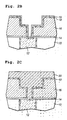
FIGS. 2A to 2D are sectional views for describing a damascene process used for manufacturing a copper inductor according to embodiments. - Referring to
FIGS. 1A to 1C, acopper inductor 100 according to embodiments is composed of five layers L1, L2, L3, L4, and L5 vertically stacked over a semiconductor (not shown). The layers include copper metal layers M1, M2, M3, M4, and M5, respectively. - The copper inductor in
FIG. 1 is described as having the five layers. However, the number of layers is not limited to five but varies in accordance with the capacity of the inductor to be integrated. The copper metal layers constitute the conductor of the inductor. - As illustrated in
FIG. 1C , in thecopper inductor 100 according to embodiments, copper metal layers are connected to each other in a rectangular spiral. The plane of the functional coils in the spiral is vertical with respect to the semiconductor substrate. - In
FIG. 1C , A and B denote both terminals of theinductor 100. As described above, since thecopper inductor 100 according to embodiments has rectangular spirals aligned to be vertical with respect to the semiconductor substrate, thecopper inductor 100 does not occupy a large amount of the horizontal space of a semiconductor chip. The copper inductor according to embodiments can be formed in a small space. For example, the inductor can be formed at a narrow and long edge region on the chip where circuit elements such as transistors are not formed. - The manufacturing processes of the
copper inductor 100 according to embodiments are as follows. - As shown in
FIG. 1B , abarrier insulating layer 110 a, a first capping layer 120 a, a fluorinated silicate glass (FSG)layer 130 a, and asecond capping layer 140 a are sequentially laminated over a semiconductor substrate and atrench 150 a is formed in the laminated layers. - A
barrier metal layer 152 a is applied over the internal wall of thetrench 150 a and acopper metal layer 160 a is formed over thebarrier metal layer 152 a to completely fill thetrench 150 a. Thecopper metal layer 160 a corresponds to the first metal interconnection M1 of theinductor 100. - Thus, the first layer L1 is formed. Although not shown in
FIG. 1A , circuit elements such as a metal oxide semiconductor (MOS) transistor are formed under thebarrier insulating layer 110 a and the circuit elements are covered with an insulating layer. - Then, the second layer L2 is formed over the first layer L1 using the same processes as the processes forming the first layer L1.
- A
barrier insulating layer 110 b, afirst capping layer 120 b, anFSG layer 130 b, and asecond capping layer 140 b are sequentially laminated over the first layer L1. - Then, after forming a
trench 150 b on the laminated layers, abarrier metal layer 152 b is applied over the internal wall of thetrench 150 b. A metal layer 160 b is formed to completely fill thetrench 150 b. The second layer L2 constitutes the second metal interconnection M2 of the inductor. - Then, the third layer L3, the fourth layer L4, and the fifth layer L5 are laminated using the above methods. The first to fifth metal interconnections M1 to M5 are connected through a double damascene structure.
- In the sectional view of
FIG. 1A , since the connection between the first metal interconnection and the second metal interconnection is not illustrated, the double damascene is not expressed with respect to the first and second metal interconnections M1 and M2. - According to embodiments, the metal interconnections are electrically connected to each other by the via portion of the metal interconnections M1 to M5.
- The formation of the metal interconnection using the double damascene process will be described with reference to
FIGS. 2A to 2D. - Referring to
FIG. 2A , abarrier insulating layer 14 is formed over a firstinterlayer dielectric layer 10 where alower metal interconnection 12 is formed. - Here, the
lower metal interconnection 12 may be one of the first to fourth metal interconnections and the firstinterlayer insulating layer 10 may refer to the first capping layer 120, the FSG layer 130, and the second capping layer 140 inFIG. 1B . - The FSG layer 130 has a low dielectric constant but emits a fluorine gas which can corrode an oxide layer. Therefore, the capping layers 120 and 140 are applied under and over the FSG layer 130 to prevent the oxide layer from being corroded by the FSG layer 130.
- The capping layers 120 and 140 are, for example, SiH4. The first
interlayer dielectric layer 10 is made as thick as necessary to make the metal interconnection layers long enough to forminductor 100. Thebarrier insulating layer 14, which may be formed of SiN or SiC, functions as an etch stop layer in the process of forming a damascene pattern. - After forming the
barrier insulating layer 14, a secondinterlayer dielectric layer 16 is formed over thebarrier insulating layer 14. The secondinterlayer dielectric layer 16 is formed using the same material and processes as the firstinterlayer dielectric layer 10. - After forming the second
interlayer dielectric layer 16, a damascene pattern composed of a via 16 a and atrench 16 b is formed in the secondinterlayer dielectric layer 16 using thebarrier insulating layer 14 as the etch stop layer. - Then, after removing a part of the
barrier insulating layer 14 exposed by a via 16 b, abarrier metal layer 18 is formed over the entire surface of the secondinterlayer dielectric layer 16. - The
barrier metal layer 18 is uniformly applied over the internal walls of the via 16 a and thetrench 16 b. Thebarrier metal layer 18 can be formed of a Ta based compound (such as TaN, or TaSiN) or other compound (such as Ti/TiN, and WNx) that is well adhered to copper and that can effectively prevent the copper from diffusing into surrounding regions. - Then, as illustrated in
FIG. 2B , acopper seed layer 19 is applied over thebarrier metal layer 18. - Then, as illustrated in
FIG. 2C , acopper layer 20 that sufficiently fills the via 16 a and thetrench 16 b is formed over thecopper seed layer 19 by an electrochemical plating (ECP) method. - Referring to
FIG. 2D , thecopper layer 20 is polished by a chemical mechanical polishing (CMP) method until the secondinterlayer dielectric layer 16 is exposed. This completes acopper metal interconnection 22. - According to embodiments, since the inductor is formed of copper, which has a low resistivity, it is possible to prevent the performance of the inductor from degrading because of a change in temperature. An additional large area is not required to accomodate the inductor in the chip. The inductor can be manufactured using a narrow area along an edge.
- Also, according to embodiments, since the integrated circuit element and the inductor are formed together on one chip, rather than forming the inductor on a separate substrate, it is possible to create a single integrated chip which includes the inductor with other devices, such as transistors.
- It will be obvious and apparent to those skilled in the art that various modifications and variations can be made in the embodiments disclosed. Thus, it is intended that the disclosed embodiments cover the obvious and apparent modifications and variations, provided that they are within the scope of the appended claims and their equivalents.
Claims (13)
1. A method comprising forming a plurality of elements of an inductor by a damascene process.
2. The method of claim 1 , wherein the inductor is a copper inductor.
3. The method of claim 1 , comprising laminating a first barrier insulating layer and first interlayer dielectric layer over a semiconductor substrate to form a first laminated layer, wherein the first barrier insulating layer and first interlayer dielectric layer are comprised in an element of the inductor.
4. The method of claim 3 , comprising:
forming a first trench in the first laminated layer;
applying a first barrier metal layer over the internal wall of the first trench; and
forming a first copper metal layer over the first barrier metal layer to completely fill the first trench to form a first metal interconnection layer.
5. The method of claim 4 , comprising:
laminating a second barrier insulating layer and a second interlayer dielectric layer over the first metal interconnection layer to form a second laminated layer;
forming a second trench having a double damascene structure in the second laminated layer; and
applying a second barrier metal layer over the internal wall of the second trench and forming a second copper metal layer over the second barrier metal layer to completely fill the second trench to form a second metal interconnection layer over the first metal interconnection layer.
6. The method of claim 5 , comprising:
laminating a third barrier insulating layer and a third interlayer dielectric layer over the second metal interconnection layer to form a third laminated layer;
forming a third trench having a double damascene structure in the third laminated layer; and
applying a third barrier metal layer over the internal wall of the third trench and forming a third copper metal layer over the third barrier metal layer to completely fill the third trench to form a third metal interconnection layer over the second metal interconnection layer.
7. The method of claim 6 , wherein the first metal layer and the second metal layer are electrically connected to each other by a via connection included in the double damascene trench structure of the second metal layer.
8. The method of claim 7 , wherein the second metal layer and the third metal layer are electrically connected to each other by a via connection included in the double damascene trench structure of the third metal layer.
9. The method of claim 8 , wherein the interlayer dielectric layer is formed of a first capping layer, a fluorinated silicate glass (FSG) layer, and a second capping layer.
10. The method of claim 9 , wherein:
the first to third metal interconnection layers form rectangular spirals, which are aligned vertically with respect to the semiconductor substrate, and
the end of the first metal interconnection layer and the end of the third metal interconnection layer are terminals of an inductor.
11. The method of claim 9 , wherein the barrier insulating layer comprises at least one of SiN and SiC.
12. An apparatus comprising a plurality of elements of an inductor having a damascene structure.
13. The apparatus of claim 12 , wherein the inductor is a copper inductor.
Applications Claiming Priority (2)
| Application Number | Priority Date | Filing Date | Title |
|---|---|---|---|
| KR10-2005-0133461 | 2005-12-29 | ||
| KR1020050134461A KR100650907B1 (en) | 2005-12-29 | 2005-12-29 | Copper metal inductor and method for fabricating the same |
Publications (1)
| Publication Number | Publication Date |
|---|---|
| US20070155152A1 true US20070155152A1 (en) | 2007-07-05 |
Family
ID=37713999
Family Applications (1)
| Application Number | Title | Priority Date | Filing Date |
|---|---|---|---|
| US11/617,197 Abandoned US20070155152A1 (en) | 2005-12-29 | 2006-12-28 | Method of manufacturing a copper inductor |
Country Status (2)
| Country | Link |
|---|---|
| US (1) | US20070155152A1 (en) |
| KR (1) | KR100650907B1 (en) |
Cited By (6)
| Publication number | Priority date | Publication date | Assignee | Title |
|---|---|---|---|---|
| US20080060185A1 (en) * | 2006-09-13 | 2008-03-13 | Dongbu Hitek Co., Ltd. | Method of manufacturing inductor |
| US20100164059A1 (en) * | 2008-12-25 | 2010-07-01 | Fujitsu Limited | Semiconductor device and manufacturing method thereof |
| US10553354B2 (en) | 2017-03-10 | 2020-02-04 | International Business Machines Corporation | Method of manufacturing inductor with ferromagnetic cores |
| CN110943072A (en) * | 2018-09-21 | 2020-03-31 | 世界先进积体电路股份有限公司 | Inductance structure |
| US10903117B2 (en) * | 2019-03-04 | 2021-01-26 | International Business Machines Corporation | Fabricating vias with lower resistance |
| US20220328237A1 (en) * | 2021-04-09 | 2022-10-13 | Qualcomm Incorporated | Three dimensional (3d) vertical spiral inductor and transformer |
Families Citing this family (2)
| Publication number | Priority date | Publication date | Assignee | Title |
|---|---|---|---|---|
| US7733207B2 (en) | 2007-05-31 | 2010-06-08 | Electronics And Telecommunications Research Institute | Vertically formed inductor and electronic device having the same |
| KR100940529B1 (en) * | 2007-05-31 | 2010-02-10 | 한국전자통신연구원 | Vertically Turned Metal Line Inductor and Electric Device including the Inductor |
Citations (5)
| Publication number | Priority date | Publication date | Assignee | Title |
|---|---|---|---|---|
| US20030013264A1 (en) * | 2000-03-06 | 2003-01-16 | Chartered Semiconductor Manufacturing Ltd. | Integrated vertical spiral inductor on semiconductor material |
| US6548396B2 (en) * | 1998-07-23 | 2003-04-15 | Applied Materials, Inc. | Method of producing an interconnect structure for an integrated circuit |
| US20030183940A1 (en) * | 2002-03-29 | 2003-10-02 | Junji Noguchi | Semiconductor device and a method of manufacturing the same |
| US20040021227A1 (en) * | 2002-07-31 | 2004-02-05 | Fujitsu Limited | Semiconductor device and method for fabricating the same |
| US20050142778A1 (en) * | 2003-12-30 | 2005-06-30 | Park Sang K. | Method for forming inductor in semiconductor device |
Family Cites Families (4)
| Publication number | Priority date | Publication date | Assignee | Title |
|---|---|---|---|---|
| JP3164025B2 (en) | 1997-08-04 | 2001-05-08 | 日本電気株式会社 | Semiconductor integrated circuit device and method of manufacturing the same |
| JP3578644B2 (en) | 1998-10-12 | 2004-10-20 | Necエレクトロニクス株式会社 | Semiconductor device |
| KR101051682B1 (en) * | 2004-05-31 | 2011-07-26 | 매그나칩 반도체 유한회사 | Inductor Formation Method of Semiconductor Device |
| KR100668220B1 (en) * | 2004-12-30 | 2007-01-11 | 동부일렉트로닉스 주식회사 | Inductor for Semiconductor Device |
-
2005
- 2005-12-29 KR KR1020050134461A patent/KR100650907B1/en not_active IP Right Cessation
-
2006
- 2006-12-28 US US11/617,197 patent/US20070155152A1/en not_active Abandoned
Patent Citations (5)
| Publication number | Priority date | Publication date | Assignee | Title |
|---|---|---|---|---|
| US6548396B2 (en) * | 1998-07-23 | 2003-04-15 | Applied Materials, Inc. | Method of producing an interconnect structure for an integrated circuit |
| US20030013264A1 (en) * | 2000-03-06 | 2003-01-16 | Chartered Semiconductor Manufacturing Ltd. | Integrated vertical spiral inductor on semiconductor material |
| US20030183940A1 (en) * | 2002-03-29 | 2003-10-02 | Junji Noguchi | Semiconductor device and a method of manufacturing the same |
| US20040021227A1 (en) * | 2002-07-31 | 2004-02-05 | Fujitsu Limited | Semiconductor device and method for fabricating the same |
| US20050142778A1 (en) * | 2003-12-30 | 2005-06-30 | Park Sang K. | Method for forming inductor in semiconductor device |
Cited By (11)
| Publication number | Priority date | Publication date | Assignee | Title |
|---|---|---|---|---|
| US20080060185A1 (en) * | 2006-09-13 | 2008-03-13 | Dongbu Hitek Co., Ltd. | Method of manufacturing inductor |
| US7568278B2 (en) * | 2006-09-13 | 2009-08-04 | Dongbu Hitek Co., Ltd. | Method of manufacturing inductor |
| US20100164059A1 (en) * | 2008-12-25 | 2010-07-01 | Fujitsu Limited | Semiconductor device and manufacturing method thereof |
| US8786086B2 (en) * | 2008-12-25 | 2014-07-22 | Fujitsu Limited | Semiconductor device including wiring having main portion and extended portion |
| US10553354B2 (en) | 2017-03-10 | 2020-02-04 | International Business Machines Corporation | Method of manufacturing inductor with ferromagnetic cores |
| US11037725B2 (en) | 2017-03-10 | 2021-06-15 | International Business Machines Corporation | Manufacturing method for inductor with ferromagnetic cores |
| US11398347B2 (en) | 2017-03-10 | 2022-07-26 | International Business Machines Corporation | Inductor with ferromagnetic cores |
| CN110943072A (en) * | 2018-09-21 | 2020-03-31 | 世界先进积体电路股份有限公司 | Inductance structure |
| US10903117B2 (en) * | 2019-03-04 | 2021-01-26 | International Business Machines Corporation | Fabricating vias with lower resistance |
| US20220328237A1 (en) * | 2021-04-09 | 2022-10-13 | Qualcomm Incorporated | Three dimensional (3d) vertical spiral inductor and transformer |
| WO2022217169A1 (en) * | 2021-04-09 | 2022-10-13 | Qualcomm Incorporated | Three dimensional (3d) vertical spiral inductor and transformer |
Also Published As
| Publication number | Publication date |
|---|---|
| KR100650907B1 (en) | 2006-11-28 |
Similar Documents
| Publication | Publication Date | Title |
|---|---|---|
| US8384224B2 (en) | Through wafer vias and method of making same | |
| US7531407B2 (en) | Semiconductor integrated circuit devices having high-Q wafer backside inductors and methods of fabricating same | |
| US10373905B2 (en) | Integrating metal-insulator-metal capacitors with air gap process flow | |
| US20070155152A1 (en) | Method of manufacturing a copper inductor | |
| US8035198B2 (en) | Through wafer via and method of making same | |
| CN1319170C (en) | Inductor device having improved quality factor | |
| KR101548664B1 (en) | Semiconductor device integrating through substrate vias into middle-of-line layers of integrated circuits | |
| US7236081B2 (en) | Inductor and method of forming the same | |
| US8299566B2 (en) | Through wafer vias and method of making same | |
| US10727124B2 (en) | Structure and method for forming fully-aligned trench with an up-via integration scheme | |
| US7786586B2 (en) | Inductor of semiconductor device and method for manufacturing the same | |
| CN101996861B (en) | Forming method of inductor | |
| US20090002114A1 (en) | Integrated inductor | |
| US7169680B2 (en) | Method for fabricating a metal-insulator-metal capacitor | |
| US7687392B2 (en) | Semiconductor device having metal wiring and method for fabricating the same | |
| US20220359387A1 (en) | Structure and method of forming a semiconductor device with resistive elements | |
| US20200243602A1 (en) | Integrated circuits with integrated memory structures and capacitors and methods for fabricating the same | |
| KR100954920B1 (en) | Inductor structure | |
| US20240105609A1 (en) | High density backside capacitor and inductor | |
| US20160260794A1 (en) | Coil inductor | |
| CN117855193A (en) | Method for forming grounding shielding layer |
Legal Events
| Date | Code | Title | Description |
|---|---|---|---|
| AS | Assignment |
Owner name: DONGBU ELECTRONICS CO., LTD., KOREA, REPUBLIC OF Free format text: ASSIGNMENT OF ASSIGNORS INTEREST;ASSIGNOR:KANG, MYUNG IL;REEL/FRAME:018692/0791 Effective date: 20061226 |
|
| STCB | Information on status: application discontinuation |
Free format text: ABANDONED -- FAILURE TO RESPOND TO AN OFFICE ACTION |