US20070212626A1 - Electrophotographic photoreceptor, and image forming apparatus and process cartridge using the same - Google Patents
Electrophotographic photoreceptor, and image forming apparatus and process cartridge using the same Download PDFInfo
- Publication number
- US20070212626A1 US20070212626A1 US11/684,520 US68452007A US2007212626A1 US 20070212626 A1 US20070212626 A1 US 20070212626A1 US 68452007 A US68452007 A US 68452007A US 2007212626 A1 US2007212626 A1 US 2007212626A1
- Authority
- US
- United States
- Prior art keywords
- group
- substituted
- compound
- photoreceptor
- independently represents
- Prior art date
- Legal status (The legal status is an assumption and is not a legal conclusion. Google has not performed a legal analysis and makes no representation as to the accuracy of the status listed.)
- Abandoned
Links
Images


Classifications
-
- G—PHYSICS
- G03—PHOTOGRAPHY; CINEMATOGRAPHY; ANALOGOUS TECHNIQUES USING WAVES OTHER THAN OPTICAL WAVES; ELECTROGRAPHY; HOLOGRAPHY
- G03G—ELECTROGRAPHY; ELECTROPHOTOGRAPHY; MAGNETOGRAPHY
- G03G5/00—Recording members for original recording by exposure, e.g. to light, to heat, to electrons; Manufacture thereof; Selection of materials therefor
- G03G5/02—Charge-receiving layers
- G03G5/04—Photoconductive layers; Charge-generation layers or charge-transporting layers; Additives therefor; Binders therefor
- G03G5/06—Photoconductive layers; Charge-generation layers or charge-transporting layers; Additives therefor; Binders therefor characterised by the photoconductive material being organic
- G03G5/07—Polymeric photoconductive materials
- G03G5/075—Polymeric photoconductive materials obtained otherwise than by reactions only involving carbon-to-carbon unsaturated bonds
- G03G5/076—Polymeric photoconductive materials obtained otherwise than by reactions only involving carbon-to-carbon unsaturated bonds having a photoconductive moiety in the polymer backbone
- G03G5/0763—Polymeric photoconductive materials obtained otherwise than by reactions only involving carbon-to-carbon unsaturated bonds having a photoconductive moiety in the polymer backbone comprising arylamine moiety
-
- G—PHYSICS
- G03—PHOTOGRAPHY; CINEMATOGRAPHY; ANALOGOUS TECHNIQUES USING WAVES OTHER THAN OPTICAL WAVES; ELECTROGRAPHY; HOLOGRAPHY
- G03G—ELECTROGRAPHY; ELECTROPHOTOGRAPHY; MAGNETOGRAPHY
- G03G5/00—Recording members for original recording by exposure, e.g. to light, to heat, to electrons; Manufacture thereof; Selection of materials therefor
- G03G5/02—Charge-receiving layers
- G03G5/04—Photoconductive layers; Charge-generation layers or charge-transporting layers; Additives therefor; Binders therefor
- G03G5/05—Organic bonding materials; Methods for coating a substrate with a photoconductive layer; Inert supplements for use in photoconductive layers
- G03G5/0528—Macromolecular bonding materials
- G03G5/0532—Macromolecular bonding materials obtained by reactions only involving carbon-to-carbon unsatured bonds
- G03G5/0542—Polyvinylalcohol, polyallylalcohol; Derivatives thereof, e.g. polyvinylesters, polyvinylethers, polyvinylamines
-
- G—PHYSICS
- G03—PHOTOGRAPHY; CINEMATOGRAPHY; ANALOGOUS TECHNIQUES USING WAVES OTHER THAN OPTICAL WAVES; ELECTROGRAPHY; HOLOGRAPHY
- G03G—ELECTROGRAPHY; ELECTROPHOTOGRAPHY; MAGNETOGRAPHY
- G03G5/00—Recording members for original recording by exposure, e.g. to light, to heat, to electrons; Manufacture thereof; Selection of materials therefor
- G03G5/02—Charge-receiving layers
- G03G5/04—Photoconductive layers; Charge-generation layers or charge-transporting layers; Additives therefor; Binders therefor
- G03G5/05—Organic bonding materials; Methods for coating a substrate with a photoconductive layer; Inert supplements for use in photoconductive layers
- G03G5/0528—Macromolecular bonding materials
- G03G5/0532—Macromolecular bonding materials obtained by reactions only involving carbon-to-carbon unsatured bonds
- G03G5/0546—Polymers comprising at least one carboxyl radical, e.g. polyacrylic acid, polycrotonic acid, polymaleic acid; Derivatives thereof, e.g. their esters, salts, anhydrides, nitriles, amides
-
- G—PHYSICS
- G03—PHOTOGRAPHY; CINEMATOGRAPHY; ANALOGOUS TECHNIQUES USING WAVES OTHER THAN OPTICAL WAVES; ELECTROGRAPHY; HOLOGRAPHY
- G03G—ELECTROGRAPHY; ELECTROPHOTOGRAPHY; MAGNETOGRAPHY
- G03G5/00—Recording members for original recording by exposure, e.g. to light, to heat, to electrons; Manufacture thereof; Selection of materials therefor
- G03G5/02—Charge-receiving layers
- G03G5/04—Photoconductive layers; Charge-generation layers or charge-transporting layers; Additives therefor; Binders therefor
- G03G5/05—Organic bonding materials; Methods for coating a substrate with a photoconductive layer; Inert supplements for use in photoconductive layers
- G03G5/0528—Macromolecular bonding materials
- G03G5/0589—Macromolecular compounds characterised by specific side-chain substituents or end groups
-
- G—PHYSICS
- G03—PHOTOGRAPHY; CINEMATOGRAPHY; ANALOGOUS TECHNIQUES USING WAVES OTHER THAN OPTICAL WAVES; ELECTROGRAPHY; HOLOGRAPHY
- G03G—ELECTROGRAPHY; ELECTROPHOTOGRAPHY; MAGNETOGRAPHY
- G03G5/00—Recording members for original recording by exposure, e.g. to light, to heat, to electrons; Manufacture thereof; Selection of materials therefor
- G03G5/02—Charge-receiving layers
- G03G5/04—Photoconductive layers; Charge-generation layers or charge-transporting layers; Additives therefor; Binders therefor
- G03G5/05—Organic bonding materials; Methods for coating a substrate with a photoconductive layer; Inert supplements for use in photoconductive layers
- G03G5/0528—Macromolecular bonding materials
- G03G5/0592—Macromolecular compounds characterised by their structure or by their chemical properties, e.g. block polymers, reticulated polymers, molecular weight, acidity
-
- G—PHYSICS
- G03—PHOTOGRAPHY; CINEMATOGRAPHY; ANALOGOUS TECHNIQUES USING WAVES OTHER THAN OPTICAL WAVES; ELECTROGRAPHY; HOLOGRAPHY
- G03G—ELECTROGRAPHY; ELECTROPHOTOGRAPHY; MAGNETOGRAPHY
- G03G5/00—Recording members for original recording by exposure, e.g. to light, to heat, to electrons; Manufacture thereof; Selection of materials therefor
- G03G5/02—Charge-receiving layers
- G03G5/04—Photoconductive layers; Charge-generation layers or charge-transporting layers; Additives therefor; Binders therefor
- G03G5/05—Organic bonding materials; Methods for coating a substrate with a photoconductive layer; Inert supplements for use in photoconductive layers
- G03G5/0528—Macromolecular bonding materials
- G03G5/0596—Macromolecular compounds characterised by their physical properties
-
- G—PHYSICS
- G03—PHOTOGRAPHY; CINEMATOGRAPHY; ANALOGOUS TECHNIQUES USING WAVES OTHER THAN OPTICAL WAVES; ELECTROGRAPHY; HOLOGRAPHY
- G03G—ELECTROGRAPHY; ELECTROPHOTOGRAPHY; MAGNETOGRAPHY
- G03G5/00—Recording members for original recording by exposure, e.g. to light, to heat, to electrons; Manufacture thereof; Selection of materials therefor
- G03G5/02—Charge-receiving layers
- G03G5/04—Photoconductive layers; Charge-generation layers or charge-transporting layers; Additives therefor; Binders therefor
- G03G5/06—Photoconductive layers; Charge-generation layers or charge-transporting layers; Additives therefor; Binders therefor characterised by the photoconductive material being organic
- G03G5/07—Polymeric photoconductive materials
- G03G5/071—Polymeric photoconductive materials obtained by reactions only involving carbon-to-carbon unsaturated bonds
- G03G5/072—Polymeric photoconductive materials obtained by reactions only involving carbon-to-carbon unsaturated bonds comprising pending monoamine groups
- G03G5/0732—Polymeric photoconductive materials obtained by reactions only involving carbon-to-carbon unsaturated bonds comprising pending monoamine groups comprising pending alkenylarylamine
-
- G—PHYSICS
- G03—PHOTOGRAPHY; CINEMATOGRAPHY; ANALOGOUS TECHNIQUES USING WAVES OTHER THAN OPTICAL WAVES; ELECTROGRAPHY; HOLOGRAPHY
- G03G—ELECTROGRAPHY; ELECTROPHOTOGRAPHY; MAGNETOGRAPHY
- G03G5/00—Recording members for original recording by exposure, e.g. to light, to heat, to electrons; Manufacture thereof; Selection of materials therefor
- G03G5/02—Charge-receiving layers
- G03G5/04—Photoconductive layers; Charge-generation layers or charge-transporting layers; Additives therefor; Binders therefor
- G03G5/06—Photoconductive layers; Charge-generation layers or charge-transporting layers; Additives therefor; Binders therefor characterised by the photoconductive material being organic
- G03G5/07—Polymeric photoconductive materials
- G03G5/071—Polymeric photoconductive materials obtained by reactions only involving carbon-to-carbon unsaturated bonds
- G03G5/074—Polymeric photoconductive materials obtained by reactions only involving carbon-to-carbon unsaturated bonds comprising pending diamine
-
- G—PHYSICS
- G03—PHOTOGRAPHY; CINEMATOGRAPHY; ANALOGOUS TECHNIQUES USING WAVES OTHER THAN OPTICAL WAVES; ELECTROGRAPHY; HOLOGRAPHY
- G03G—ELECTROGRAPHY; ELECTROPHOTOGRAPHY; MAGNETOGRAPHY
- G03G5/00—Recording members for original recording by exposure, e.g. to light, to heat, to electrons; Manufacture thereof; Selection of materials therefor
- G03G5/02—Charge-receiving layers
- G03G5/04—Photoconductive layers; Charge-generation layers or charge-transporting layers; Additives therefor; Binders therefor
- G03G5/06—Photoconductive layers; Charge-generation layers or charge-transporting layers; Additives therefor; Binders therefor characterised by the photoconductive material being organic
- G03G5/07—Polymeric photoconductive materials
- G03G5/071—Polymeric photoconductive materials obtained by reactions only involving carbon-to-carbon unsaturated bonds
- G03G5/0745—Polymeric photoconductive materials obtained by reactions only involving carbon-to-carbon unsaturated bonds comprising pending hydrazone
-
- G—PHYSICS
- G03—PHOTOGRAPHY; CINEMATOGRAPHY; ANALOGOUS TECHNIQUES USING WAVES OTHER THAN OPTICAL WAVES; ELECTROGRAPHY; HOLOGRAPHY
- G03G—ELECTROGRAPHY; ELECTROPHOTOGRAPHY; MAGNETOGRAPHY
- G03G5/00—Recording members for original recording by exposure, e.g. to light, to heat, to electrons; Manufacture thereof; Selection of materials therefor
- G03G5/14—Inert intermediate or cover layers for charge-receiving layers
- G03G5/147—Cover layers
- G03G5/14708—Cover layers comprising organic material
- G03G5/14713—Macromolecular material
- G03G5/14717—Macromolecular material obtained by reactions only involving carbon-to-carbon unsaturated bonds
- G03G5/1473—Polyvinylalcohol, polyallylalcohol; Derivatives thereof, e.g. polyvinylesters, polyvinylethers, polyvinylamines
-
- G—PHYSICS
- G03—PHOTOGRAPHY; CINEMATOGRAPHY; ANALOGOUS TECHNIQUES USING WAVES OTHER THAN OPTICAL WAVES; ELECTROGRAPHY; HOLOGRAPHY
- G03G—ELECTROGRAPHY; ELECTROPHOTOGRAPHY; MAGNETOGRAPHY
- G03G5/00—Recording members for original recording by exposure, e.g. to light, to heat, to electrons; Manufacture thereof; Selection of materials therefor
- G03G5/14—Inert intermediate or cover layers for charge-receiving layers
- G03G5/147—Cover layers
- G03G5/14708—Cover layers comprising organic material
- G03G5/14713—Macromolecular material
- G03G5/14717—Macromolecular material obtained by reactions only involving carbon-to-carbon unsaturated bonds
- G03G5/14734—Polymers comprising at least one carboxyl radical, e.g. polyacrylic acid, polycrotonic acid, polymaleic acid; Derivatives thereof, e.g. their esters, salts, anhydrides, nitriles, amides
-
- G—PHYSICS
- G03—PHOTOGRAPHY; CINEMATOGRAPHY; ANALOGOUS TECHNIQUES USING WAVES OTHER THAN OPTICAL WAVES; ELECTROGRAPHY; HOLOGRAPHY
- G03G—ELECTROGRAPHY; ELECTROPHOTOGRAPHY; MAGNETOGRAPHY
- G03G5/00—Recording members for original recording by exposure, e.g. to light, to heat, to electrons; Manufacture thereof; Selection of materials therefor
- G03G5/14—Inert intermediate or cover layers for charge-receiving layers
- G03G5/147—Cover layers
- G03G5/14708—Cover layers comprising organic material
- G03G5/14713—Macromolecular material
- G03G5/14786—Macromolecular compounds characterised by specific side-chain substituents or end groups
-
- G—PHYSICS
- G03—PHOTOGRAPHY; CINEMATOGRAPHY; ANALOGOUS TECHNIQUES USING WAVES OTHER THAN OPTICAL WAVES; ELECTROGRAPHY; HOLOGRAPHY
- G03G—ELECTROGRAPHY; ELECTROPHOTOGRAPHY; MAGNETOGRAPHY
- G03G5/00—Recording members for original recording by exposure, e.g. to light, to heat, to electrons; Manufacture thereof; Selection of materials therefor
- G03G5/14—Inert intermediate or cover layers for charge-receiving layers
- G03G5/147—Cover layers
- G03G5/14708—Cover layers comprising organic material
- G03G5/14713—Macromolecular material
- G03G5/14791—Macromolecular compounds characterised by their structure, e.g. block polymers, reticulated polymers, or by their chemical properties, e.g. by molecular weight or acidity
-
- G—PHYSICS
- G03—PHOTOGRAPHY; CINEMATOGRAPHY; ANALOGOUS TECHNIQUES USING WAVES OTHER THAN OPTICAL WAVES; ELECTROGRAPHY; HOLOGRAPHY
- G03G—ELECTROGRAPHY; ELECTROPHOTOGRAPHY; MAGNETOGRAPHY
- G03G5/00—Recording members for original recording by exposure, e.g. to light, to heat, to electrons; Manufacture thereof; Selection of materials therefor
- G03G5/14—Inert intermediate or cover layers for charge-receiving layers
- G03G5/147—Cover layers
- G03G5/14708—Cover layers comprising organic material
- G03G5/14713—Macromolecular material
- G03G5/14795—Macromolecular compounds characterised by their physical properties
Definitions
- Exemplary aspects of the present invention relate to an electrophotographic photoreceptor.
- exemplary aspects of the present invention relate to an image forming apparatus and a process cartridge using the electrophotographic photoreceptor.
- Organic photoreceptors are widely used as an electrophotographic photoreceptor (hereinafter referred to as photoreceptor). Organic photoreceptors typically have the following advantages over inorganic photoreceptors.
- Organic photoreceptors are capable of using materials responsive to various light (e.g., visible light, infrared light) irradiators, which are easily developed;
- various light e.g., visible light, infrared light
- organic photoreceptors are easily abraded or scratched after long repeated use because of having poor physical and chemical strength.
- An electrophotographic image forming apparatus typically includes a photoreceptor, a charger for charging the photoreceptor, an image former for forming an electrostatic latent image on the charged photoreceptor, an image developer for adhering a toner to an image portion of the electrostatic latent image, and a transferrer for transferring the toner adhered to the image portion onto a transfer medium, and optionally includes a cleaner for removing toner particles remaining on the surface of the photoreceptor which are not transferred. Such toner particles remaining on the surface of the photoreceptor contribute to image deterioration. Therefore, most image forming apparatuses include the cleaner.
- a brush cleaner As the cleaner, a brush cleaner, a magnetic brush cleaner, and a blade cleaner are typically used.
- polyester and acrylic fibers are typically used. These fibers may be shaped like a loop, a straight hair, etc., and hardness and diameter thereof may be optimized for use in the brush cleaner.
- it is difficult to completely remove toner particles by the brush cleaner because ultrafine particles tend to slip through fibers.
- the magnetic brush cleaner to which an electric field is applied so as to electrostatically remove toner particles has been proposed. In this case, there is a problem that toner particles tend to be scattered due to the electrostatic force and then adhere to the photoreceptor again.
- a blade cleaner using an elastic blade that can remove remaining toner particles (especially those having a smaller particle diameter) and that can be manufactured at a low cost, are mainly used at present.
- the blade cleaner slides over the surface of the photoreceptor while contacting therewith. Therefore, the surface of the photoreceptor tends to be mechanically abraded or scratched.
- JP-A 2002-139859 discloses a photoreceptor including an electroconductive substrate, a photosensitive layer overlaid thereon, and a protective layer including a filler overlaid thereon in this order.
- JP-A 2001-125286 and JP-A 2001-324857 have disclosed photoreceptors of which the hardness of the surface is increased, used in combination with a charger including a magnetic brush.
- a charger including a magnetic brush.
- magnetic particles of the magnetic brush are involuntarily transferred onto the photoreceptor, and then pressed thereon in the transfer process and the cleaning process, resulting in scratches being made on the surface of the photoreceptor.
- JP-A 2003-98708 discloses an image forming apparatus including a blade cleaner and a photoreceptor of which the hardness of the surface is increased in order to prevent the abrasion thereof.
- a method in which the outermost layer of a photoreceptor includes a cross-linking material, such as a thermosetting resin and an ultraviolet (UV) curing resin is proposed.
- a cross-linking material such as a thermosetting resin and an ultraviolet (UV) curing resin
- JP-A 05-181299, 2002-6526, and JP-A 2002-82465 have disclosed photoreceptors, the outermost layer of which includes a thermosetting resin as a binder resin so as to improve abrasion resistance and scratch resistance thereof.
- JP-A 2000-284514, JP-A 2000-284515, and JP-A 2001-194813 have disclosed photoreceptors including a siloxane resin having a cross-linking structure as a charge transport material so as to improve abrasion resistance and scratch resistance thereof.
- the above-mentioned JP 3286704 discloses a photoreceptor, the outermost layer of which includes a polyfunctional acrylate monomer.
- a charge transport material used together therewith there may be a case where the charge transport material and the resultant polymer obtained from the above monomer are incompatible. In this case, the low-molecular-weight components may bleed out and mechanical strength of the outermost layer may deteriorate.
- a technique in which a polycarbonate resin is added to the outermost layer is disclosed therein.
- the content of the polyfunctional acrylate monomer in the outermost layer relatively decreases.
- mechanical durability and abrasion resistance of the resultant photoreceptor deteriorate.
- the outermost layer can be much thinner when the outermost layer includes no charge transport material.
- such a thin outermost layer may disappear by abrasion in a short time.
- the life of a photoreceptor having an outermost layer is determined by a time that elapses before the outermost layer disappears by abrasion. Therefore, such a photoreceptor having a thin outermost layer cannot be a long-life photoreceptor.
- JP 3194392 discloses a photoreceptor having a charge transport layer formed by applying a coating liquid including a monomer having a carbon-carbon double bond, a charge transport material having a carbon-carbon double bond, and a binder resin.
- the binder resin may be both of a compound having a carbon-carbon double bond which is reactive to the charge transport material, and a compound having no carbon-carbon double bond which is not reactive to the charge transport material. It is described therein that such a photoreceptor has a good combination of abrasion resistance and electrical properties.
- the binder resin and the reaction product of the monomer with the charge transport material may have poor compatibility, and therefore the layer tend to separate and decrease the smoothness of the surface.
- the resultant photoreceptor has poor cleanability and the resultant image quality deteriorates.
- difunctional compounds are disclosed therein, but it is difficult to obtain a high cross-linking density by using these compounds, and therefore the resultant photoreceptor has poor abrasion resistance.
- triphenylamine materials which are widely used as a charge transport material, typically absorb short-wavelength light (such as ultraviolet ray), and thereby form complexes or get denatured. As a result, charge transport ability tends to deteriorate and a charge trap tends to be formed. Since materials composing organic photoreceptors have poor resistance to heat and light, oxidizing gas resistance tends to deteriorate and cause image density unevenness.
- Image density unevenness occurs when chargeability of a photoreceptor deteriorates due to an influence of an oxidizing gas and when surface resistance of a photoreceptor decreases by accretion of an ionic material thereon.
- the photoreceptor cannot be charged to a desired potential level, resulting in increasing image density in a low potential portion of the resultant image.
- an electrostatic latent image cannot be kept on the photoreceptor due to the low surface resistance thereof, resulting in deterioration of image density of the resultant image.
- the former case i.e., deterioration of chargeability of the photoreceptor
- deterioration of chargeability of the photoreceptor may occur due to deterioration of the constituent material, which is caused by diffusion of an oxidizing gas produced by a charger into the inner portion of the photoreceptor.
- a cross-linked outermost layer is considered to have high gas permeability because the layer is contracted when cross-linked. Therefore, a photoreceptor having the cross-linked outermost layer easily causes deterioration of the constituent material compared with that formed of a thermoplastic resin.
- the latter case (i.e., deterioration of surface resistance of the photoreceptor) may occur due to accretion and adsorption of an ionic material originated from an oxidizing gas produced by a charger on the surface of the photoreceptor.
- charges of the electrostatic latent image laterally migrate on the surface of the photoreceptor.
- a related art photoreceptor has poor mechanical durability and is easily abraded, it is easy to remove the accretion of the ionic material therefrom by applying a mechanical external force thereto using a cleaning blade. Therefore, image density unevenness rarely occurs. Even if image density unevenness occurs, it can recover in a short time. In contrast, it is difficult to remove the accretion of the ionic material from a photoreceptor having good mechanical durability because the surface thereof is hardly abraded. Therefore, image density unevenness obviously occurs and rarely recovers.
- JP-A 2004-317944 discloses a photoreceptor of which a charge transport layer includes an oxidation inhibitor.
- JP-A 2004-240047 discloses a photoreceptor of which a cross-linked outermost layer includes an oxidation inhibitor. Whether the oxidation inhibitor functions or not depends on the added amount thereof, and therefore a large amount of the oxidation inhibitor is needed to exerts its effect. Since the oxidation inhibitor has no charge transport ability, the charge transport ability deteriorates as the added amount of the oxidation inhibitor increases.
- the oxidation inhibitor typically has high charge acceptability so as to interact with an oxidizing gas, etc., and therefore a material which mainly cross-links by a radial polymerization reaction tends to be prevented from cross-linking thereby. It is difficult to obtain a photoreceptor which simultaneously satisfies charge transport ability, abrasion resistance, and oxidizing gas resistance when the oxidation inhibitor is used.
- a photoreceptor having a cross-linked outermost layer has good mechanical durability and abrasion resistance, and therefore it can be used for a long time.
- such a photoreceptor has a disadvantage in producing high quality images.
- In order to obtain a high-durable photoreceptor it is necessary to take measures against deterioration of the constituent materials.
- an initiator which needs a smaller amount of energy may be used.
- an initiator having a lower half-life temperature may be used.
- an initiator having high efficiency in a lower illuminance and an initiator generating a large amount of radical under a lower exposure may be used.
- cross-linking density of the resultant outermost layer decreases.
- the kind of the initiators are not widely used.
- exemplary aspects of the present invention provide an electrophotographic photoreceptor having a good combination of a mechanical durability and an oxidizing gas resistance.
- Exemplary aspects of the present invention provide an image forming apparatus and a process cartridge which can produce high quality images having high image density without causing image density unevenness for a long period of the time.
- an electrophotographic photoreceptor including an electroconductive substrate, a photosensitive layer located overlying the electroconductive substrate, and an outermost layer located overlying the photosensitive layer.
- the outermost layer is formed by a reaction between a radical polymerizable compound having no charge transport structure and including a compound represented by the following formula (1),
- At least one of the photosensitive layer and the outermost layer includes at least one member selected from (A) an arylmethane compound having an alkylamino group, (B) a compound represented by the following formula (2),
- R 1 , R 2 , R 3 , R 4 , R 5 , and R 6 independently represents a hydrogen atom or a group represented by the following formula:
- R 7 represents a single bond, an alkylene group, an alkylene ether group, a polyoxyalkylene group, an alkylene ether group substituted with a hydroxyl group, an alkylene ether group substituted with a (meth)acryloyloxy group, an oxyalkylene carbonyl group, or a poly(oxyalkylene carbonyl) group; and R 8 represents a hydrogen atom or a methyl group,
- R 1 , R 2 , R 3 , R 4 , R 5 , and R 6 do not simultaneously represent hydrogen atoms:
- Each of R 9 and R 10 independently represents a substituted or unsubstituted aryl group or a substituted or unsubstituted alkyl group. R 9 and R 10 optionally share bond connectivity to form a heterocyclic group containing a nitrogen atom.
- Each of Ar 1 and Ar 2 independently represents a substituted or unsubstituted aryl group.
- Each of k and m independently represents an integer of from 0 to 3, wherein both of k and m does not simultaneously represent 0; and n represents an integer of from 1 to 3.
- Each of R 11 and R 12 independently represents a substituted or unsubstituted alkyl group or a substituted or unsubstituted aryl group, wherein at least one of R 11 and R 12 is a substituted or unsubstituted aryl group, and wherein R 11 and R 12 optionally share bond connectivity to form a substituted or unsubstituted heterocyclic group containing a nitrogen atom.
- Ar 3 represents a substituted or unsubstituted aryl group.
- Exemplary aspects of the invention include an image forming apparatus and a process cartridge using the electrophotographic photoreceptor.
- FIGS. 1 to 3 are schematic views illustrating cross-sections of exemplary embodiments of an electrophotographic photoreceptor of the present invention
- FIG. 4 is a schematic view illustrating an exemplary embodiment of an image forming apparatus of the present invention.
- FIG. 5 is a schematic view illustrating an exemplary embodiment of a process cartridge of the present invention.
- the surface of a photoreceptor can be prevented from being abraded or scratched even after a long repeated use when mechanical strengths (such as hardness and elastic power) thereof are large.
- mechanical strengths such as hardness and elastic power
- a cross-linking material which binds molecules with each other, can increase mechanical strength.
- the cross-linking material can exert various effects by changing the structure of the functional group, the molecular structure, and the number of the functional groups, etc. Since the cross-linking material can be molecular-designed so as to improve not only mechanical strength but also electrical properties of the resultant photoreceptor, such materials have been widely used for electrophotographic photoreceptors.
- a photoreceptor having an outermost layer formed from a cross-linking material has excellent mechanical durability, and thereby occurrence of image defects, which are caused when the photoreceptor is abraded or scratched, can be largely decreased.
- the cross-linking material is cross-linked upon application of energy (such as heat and light), materials constituting a photosensitive layer tend to deteriorate thereby.
- electrical properties and oxidizing gas resistance deteriorate and image density unevenness is caused in the resultant image.
- the image density unevenness is caused by deterioration of the surface resistance or the bulk resistance of the photoreceptor, which is caused by accretion or adsorption of an oxidizing gas, such as NOx produced by an electric discharge of a charger and an ionic material produced from the reaction of the oxidizing gas with other compounds. Since related art photoreceptors have poor mechanical durability, the surface thereof can be easily refaced by applying a mechanical external force using a cleaning blade. Therefore, even if image density unevenness occurs, it can recover in a short time.
- an oxidizing gas such as NOx produced by an electric discharge of a charger and an ionic material produced from the reaction of the oxidizing gas with other compounds.
- a photoreceptor having an outermost layer which has good mechanical durability is hardly abraded or scratched for a long period of the time even if a mechanical external force is applied thereto.
- an electrophotographic photoreceptor including an electroconductive substrate, a photosensitive layer located overlying the electroconductive substrate, and an outermost layer located overlying the photosensitive layer.
- the outermost layer is formed by a reaction between a radical polymerizable compound having no charge transport structure and includes a compound represented by the formula (1), and a radical polymerizable compound having a charge transport structure, while applying at least one member selected from the group consisting of heat, light, and ionizing radiation to the reaction.
- At least one of the photosensitive layer and the outermost layer includes at least one member selected from (A) an arylmethane compound having an alkylamino group, (B) a compound represented by the formula (2), (C) a compound represented by the formula (3), and (D) a compound represented by the formula (4).
- a photoreceptor of an exemplary embodiment of the present invention is a multi-layered photoreceptor including an electroconductive substrate, and a photosensitive layer and an outermost layer overlaid on the electroconductive substrate in this order.
- the photosensitive layer may be either a single-layered or multi-layered so long as having a charge generation mechanism and a charge transport mechanism.
- first layer may be in direct contact with the second layer, or there may be one or more intervening layers between the first and second layer, with the second layer being closer to the substrate than the first layer.
- FIG. 1 is a cross-sectional view illustrating an exemplary embodiment of the photoreceptor of the present invention having a single-layered photosensitive layer.
- This photoreceptor includes an electroconductive substrate 31 , a photosensitive layer 34 overlaid on the electroconductive substrate 31 and including a charge generation material and a charge transport material, and an outermost layer 35 overlaid on the photosensitive layer 34 .
- the outermost layer 35 represents the after-mentioned cross-linked outermost layer.
- FIGS. 2 and 3 are cross-sectional views illustrating exemplary embodiments of the photoreceptor of the present invention having a multi-layered photosensitive layer.
- Each of these photoreceptors includes an electroconductive substrate 31 ; a charge generation layer 32 and a charge transport layer 33 overlaid on the electroconductive substrate 31 ; and an outermost layer 35 .
- the charge generation layer 32 and the charge transport layer 33 may be either overlaid on the electroconductive substrate 31 in this order (i.e., FIG. 3 ) or the reverse order (i.e., FIG. 2 ).
- the photosensitive layer and/or the outermost layer of the photoreceptor of the exemplary embodiment of the present invention includes at least one member selected from:
- the above compounds can impart oxidizing gas resistance to the resultant photoreceptor without causing deterioration of charge transport ability, inhibition of cross-linking, and decrease of hardness, which tend to be caused when an oxidation inhibitor is used.
- arylmethane compounds having an alkylamino group include the following compounds represented by the formulae (5) to (8).
- Each of R 13 and R 14 independently represents an alkyl group having 1 to 4 carbon atoms which may be substituted with an aryl group, wherein R 13 and R 14 optionally share bond connectivity to form a heterocyclic group containing a nitrogen atom.
- Each of R 15 and R 16 independently represents a hydrogen atom, a substituted or unsubstituted alkyl group having 1 to 11 carbon atoms, or a substituted or unsubstituted aryl group.
- Each of Ar 4 and Ar 5 independently represents a substituted or unsubstituted aryl group.
- Each of m and n independently represents an integer of from 0 to 3, wherein both of m and n does not simultaneously represent 0.
- Each of R 13 and R 14 independently represents an alkyl group having 1 to 4 carbon atoms which may be substituted with an aryl group. R 13 and R 14 optionally share bond connectivity to form a heterocyclic group containing a nitrogen atom.
- R 15 represents a hydrogen atom, a substituted or unsubstituted alkyl group having 1 to 11 carbon atoms, or a substituted or unsubstituted aryl group.
- Each of Ar 4 , Ar 5 , Ar 6 , Ar 7 , and Ar 8 independently represents a substituted or unsubstituted aryl group, wherein Ar 7 optionally shares bond connectivity with Ar 6 or Ar 8 to form a heterocyclic group containing a nitrogen atom.
- Each of m and n independently represents an integer of from 0 to 3, wherein both of m and n does not simultaneously represent 0.
- Each of R 13 and R 14 independently represents an alkyl group having 1 to 4 carbon atoms which may be substituted with an aryl group, wherein R 13 and R 14 optionally share bond connectivity to form a heterocyclic group containing a nitrogen atom.
- Each of Ar 4 , Ar 5 , Ar 6 , Ar 7 , and Ar 8 independently represents a substituted or unsubstituted aryl group, wherein Ar 7 optionally shares bond connectivity with Ar 6 or Ar 8 to form a heterocyclic group containing a nitrogen atom.
- Each of m and n independently represents an integer of from 0 to 3, wherein both of m and n does not simultaneously represent 0.
- R 13 and R 14 independently represents an alkyl group having 1 to 4 carbon atoms which may be substituted with an aryl group.
- R 13 and R 14 optionally share bond connectivity to form a heterocyclic group containing a nitrogen atom.
- Each of Ar 4 , Ar 6 , Ar 7 , and Ar 8 independently represents a substituted or unsubstituted aryl group.
- Ar 7 optionally shares bond connectivity with Ar 6 or Ar 8 to form a heterocyclic group containing a nitrogen atom.
- n represents an integer of from 1 to 3.
- the arylmethane compound having an alkylamino group can reduce the likelihood or prevent occurrence of image density unevenness. It is considered that the amino groups substituted with R 13 and R 14 can effectively reduce the likelihood or prevent the oxidizing gas from producing a radical substance. Since the compounds represented by the formulae (5) to (8) have a charge transport structure, charges are not trapped therein, and therefore deterioration of electric property (such as increase of residual potential) hardly occurs.
- alkyl groups represented by R 13 and R 14 include, but are not limited to, methyl group, ethyl group, propyl group, and butyl group.
- aryl groups included in R 13 and R 14 and represented by Ar 4 to Ar 8 include, but are not limited to, aromatic hydrocarbon groups derived from aromatic hydrocarbon rings (e.g., benzene, naphthalene, anthracene, pyrene) having 1 to 6 valences; and aromatic heterocyclic groups derived from aromatic heterocyclic rings (e.g., pyridine, quinoline, thiophene, furan, oxazole, oxadiazole, carbazole) having 1 to 6 valences.
- substituent groups thereof include, but are not limited to, alkyl groups (e.g., methyl group, ethyl group, propyl group, butyl group), alkoxy groups (e.g., methoxy group, ethoxy group, propoxy group, butoxy group), halogen atoms (e.g., fluorine atom, chlorine atom, bromine atom, iodine atom), and aryl groups.
- substituent groups thereof include, but are not limited to, alkyl groups (e.g., methyl group, ethyl group, propyl group, butyl group), alkoxy groups (e.g., methoxy group, ethoxy group, propoxy group, butoxy group), halogen atoms (e.g., fluorine atom, chlorine atom, bromine atom, iodine atom), and aryl groups.
- heterocyclic groups containing a nitrogen atom formed of R 13 and R 14 include, but are not limited
- heterocyclic groups containing a nitrogen atom formed of combinations of Ar 6 and Ar 7 , or Ar 7 and Ar 8 include, but are not limited to, aromatic heterocyclic groups derived from N-methyl carbazole, N-ethyl carbazole, N-phenyl carbazole, indole, and quinoline.
- Suitable compounds represented by the formulae (5), (6), (7), and (8) include the following compounds shown in Tables 1, 2, 3, and 4, respectively, but are not limited thereto.
- the compounds represented by the formulae (2) and (3) can reduce the likelihood or prevent the occurrence of image density unevenness. It is considered that the amino groups substituted with R 9 and R 10 can reduce the likelihood or prevent the oxidizing gas from producing a radical substance. Since the compounds represented by the formulae (2) and (3) have a charge transport structure, charges are not trapped therein, and therefore deterioration of electric property (such as increase of residual potential) hardly occurs.
- Each of R 9 and R 10 independently represents a substituted or unsubstituted aryl group or a substituted or unsubstituted alkyl group, R 9 and R 10 optionally share bond connectivity to form a heterocyclic group containing a nitrogen atom.
- Each of Ar 1 and Ar 2 independently represents a substituted or unsubstituted aryl group.
- Each of k and m independently represents an integer of from 0 to 3. Both of k and m does not simultaneously represent 0 and n represents an integer of from 1 to 3.
- aryl groups represented by R 9 and R 10 include, but are not limited to, aromatic hydrocarbon groups derived from aromatic hydrocarbon rings, such as benzene, naphthalene, anthracene, and pyrene.
- alkyl groups represented by R 9 and R 10 include, but are not limited to, methyl group, ethyl group, propyl group, butyl group, hexyl group, and undecanyl group. Among these, alkyl groups having 1 to 4 carbon atoms may be used.
- aryl groups represented by Ar 1 and Ar 2 include, but are not limited to, aromatic hydrocarbon groups derived from aromatic hydrocarbon rings (e.g., benzene, naphthalene, anthracene, pyrene) having 1 to 4 valences; and aromatic heterocyclic groups derived from aromatic heterocyclic rings (e.g., pyridine, quinoline, thiophene, furan, oxazole, oxadiazole, carbazole) having 1 to 4 valences.
- aromatic hydrocarbon groups derived from aromatic hydrocarbon rings e.g., benzene, naphthalene, anthracene, pyrene
- aromatic heterocyclic groups derived from aromatic heterocyclic rings e.g., pyridine, quinoline, thiophene, furan, oxazole, oxadiazole, carbazole having 1 to 4 valences.
- substituent groups thereof include, but are not limited to, alkyl groups (e.g., methyl group, ethyl group, propyl group, butyl group, hexyl group, undecanyl group), alkoxy groups (e.g., methoxy group, ethoxy group, propoxy group, butoxy group), halogen atoms (e.g., fluorine atom, chlorine atom, bromine atom, iodine atom), and aryl groups.
- alkyl groups e.g., methyl group, ethyl group, propyl group, butyl group, hexyl group, undecanyl group
- alkoxy groups e.g., methoxy group, ethoxy group, propoxy group, butoxy group
- halogen atoms e.g., fluorine atom, chlorine atom, bromine atom, iodine atom
- heterocyclic group containing a nitrogen atom formed of R 9 and R 10 include, but are not limited to, pyrrolidinyl group, piperidinyl group, pyrrolinyl group, and aromatic heterocyclic group derived from N-methyl carbazole, N-ethyl carbazole, N-phenyl carbazole, indole, and quinoline.
- Suitable compounds represented by the formulae (2) and (3) include the following compounds shown in Tables 5 and 6, respectively, but are not limited thereto.
- the compounds represented by the formulae (2) and (3) further include compounds disclosed in published examined Japanese patent application No. (hereinafter referred to as JP-B) 58-57739 and JP 2529299.
- the compound represented by the formula (2) can be prepared by so-called Wittig reaction or Wittig-Horner reaction in which a triphenyl phosphonium salt or a phosphonic acid ester, respectively, is reacted with an aldehyde.
- the compound represented by the formula (3) can be prepared by reduction of the compound represented by the formula (2).
- Diamine compounds represented by the formula (4) are disclosed in JP-B 62-13382, and U.S. Pat. Nos. 4,223,144, 3,271,383, and 3,291,788 as an intermediate of a dye or a precursor of a polymer.
- R 11 and R 12 independently represents a substituted or unsubstituted alkyl group or a substituted or unsubstituted aryl group. At least one of R 11 and R 12 is a substituted or unsubstituted aryl group. R 11 and R 12 optionally share bond connectivity to form a substituted or unsubstituted heterocyclic group containing a nitrogen atom.
- Ar 3 represents a substituted or unsubstituted aryl group.
- the resultant image quality is maintained in good level even after the photoreceptor is repeatedly used.
- the mechanism is considered as follows. Because an alkylamino group included in the compound has strong basic properties, an oxidizing gas and an ionic substance which are considered to cause image density unevenness can be neutralized thereby.
- the diamine compound used for exemplary embodiments of the present invention has good charge transport ability because of having an amino group substituted with an aryl group, which is known as a functional group having good charge transport ability (described in a technical document “Guiding concept for developing better charge transporting organic materials”, Takahashi et al., Electrophotography (DENSHISHY ASHIN GAKKAISHI), Vol. 25, No. 3, p. 16 (1983)).
- the photoreceptor when a photoreceptor includes the diamine compounds together with another charge transport material, the photoreceptor has better sensitivity and stability even after repeated use.
- the diamine compound represented by the formula (4) can be easily prepared by the method described in a technical document “A new synthesis of bisbenzils and novel poly(phenylquinoxaline)s therefrom”, E. Elce and A. S. Hay, Polymer, Vol. 37, No. 9, 1745 (1996). Specifically, a dihalogen compound represented by the following formula (12) is reacted with a secondary amine compound represented by the following formula (13) in the presence of a basic compound at a temperature of from room temperature to about 100° C.:
- Ar 3 represents a substituted or unsubstituted aryl group and B represents a halogen atom.
- Each of R 11 and R 12 independently represents a substituted or unsubstituted alkyl group or a substituted or unsubstituted aryl group. At least one of R 11 and R 12 is a substituted or unsubstituted aryl group, and wherein R 11 and R 12 optionally share bond connectivity to form a substituted or unsubstituted heterocyclic group containing a nitrogen atom.
- the basic compounds include, but are not limited to, potassium carbonate, sodium carbonate, potassium hydroxide, sodium hydroxide, sodium hydride, sodium methylate, and potassium t-butoxide.
- reaction solvents include, but are not limited to, dioxane, tetrahydrofuran, toluene, xylene, dimethyl sulfoxide, N,N-dimethyl formamide, N-methylpyrrolidone, 1,3-dimethyl-2-imidazolidinone, and acetonitrile.
- alkyl groups represented by R 11 and R 12 included in the formulae (4) and (13) include, but are not limited to, methyl group, ethyl group, propyl group, butyl group, hexyl group, and undecanyl group.
- aromatic group represented by R 11 , R 12 , and Ar 3 included in the formulae (4) and (12) include, but are not limited to, aromatic hydrocarbon groups derived from aromatic hydrocarbon rings such as benzene, biphenyl, naphthalene, anthracene, fluorene, and pyrene; and aromatic heterocyclic groups derived from aromatic heterocyclic rings such as pyridine, quinoline, thiophene, furan, oxazole, oxadiazole, and carbazole.
- substituent groups thereof include, but are not limited to, alkyl groups (e.g., methyl group, ethyl group, propyl group, butyl group, hexyl group, undecanyl group), alkoxy groups (e.g., methoxy group, ethoxy group, propoxy group, butoxy group), halogen atoms (e.g., fluorine atom, chlorine atom, bromine atom, iodine atom), aryl groups, and heterocyclic groups derived from heterocyclic rings such as pyrrolidine, piperidine, and piperazine.
- alkyl groups e.g., methyl group, ethyl group, propyl group, butyl group, hexyl group, undecanyl group
- alkoxy groups e.g., methoxy group, ethoxy group, propoxy group, butoxy group
- halogen atoms e.g., fluorine atom, chlorine atom, bromine
- heterocyclic group containing a nitrogen atom formed of R 11 and R 12 include, but are not limited to, condensed heterocyclic groups to which an aryl group is bound to heterocyclic groups, such as pyrrolidinyl group, piperidinyl group, and pyrrolinyl group.
- Suitable compounds represented by the formula (4) include the following compounds shown in Table 7, but are not limited thereto.
- the above-mentioned compounds i.e., (A) an arylmethane compound having an alkylamino group; (B) a compound represented by the formula (2); (C) a compound represented by the formula (3); and (D) a compound represented by the formula (4)
- A an arylmethane compound having an alkylamino group
- B a compound represented by the formula (2)
- C a compound represented by the formula (3)
- D a compound represented by the formula (4)
- the layer may include the compound in an amount of from 0.01 to 150% by weight based on total weight of the layer, but the amount is not limited thereto as long as the photoreceptor has good electric and mechanical properties.
- the amount is too small, the resultant photoreceptor does not have sufficient oxidizing gas resistance.
- the amount is too large, the resultant photoreceptor has sufficient oxidizing gas resistance, but does not have sufficient oxidizing gas resistance.
- the radical polymerizable compound having no charge transport structure for use in exemplary embodiments of the present invention is represented by the formula (1).
- R 1 , R 2 , R 3 , R 4 , R 5 , and R 6 independently represents a hydrogen atom or a group represented by the following formula:
- R 7 represents a single bond, an alkylene group, an alkylene ether group, a polyoxyalkylene group, an alkylene ether group substituted with a hydroxyl group, an alkylene ether group substituted with a (meth)acryloyloxy group, an oxyalkylene carbonyl group, or a poly(oxyalkylene carbonyl) group; and R 8 represents a hydrogen atom or a methyl group.
- R 1 , R 2 , R 3 , R 4 , R 5 , and R 6 do not simultaneously represent hydrogen atoms.
- R 7 is preferably a single bond or an alkylene ether group substituted with a hydroxyl group.
- a compound having 5 or more acryloyloxy or methacryloyloxy groups as radical polymerizable functional groups may be used.
- a compound having 5 or more acryloyloxy groups can be prepared by subjecting a compound having 5 or more hydroxyl group and a member selected from an acrylic acid, an acrylate, an acrylic halide, and an acrylic ester to an esterification reaction or an interesterification reaction.
- a compound having 5 or more methacryloyloxy groups can be prepared in the same manner.
- Each of the 5 or more radial polymerizable groups may be the same or different.
- R 1 , R 2 , R 3 , R 4 , R 5 , and R 6 of the compound represented by the formula (1) include, but are not limited to, the following combinations:
- Suitable compounds represented by the formula (1) include the following compounds shown in Table 8, but are not limited thereto.
- These compounds can be prepared by esterification of polyols, and this method has high yield, low manufacturing cost, and high manufacturability.
- a compound having 6 radical polymerizable functional groups When 2 to 4 of the compounds are used in combination and a compound having 6 radical polymerizable functional groups is included therein, a mixture of a compound having 6 radical polymerizable functional groups which are esterified and a compound having 5 radical polymerizable functional groups and 1 hydrogen group which is unesterified may be used, because of high yield thereof.
- the mixture may include the compound having 6 radical polymerizable functional groups in an amount of from 20 to 99% by weight, more preferably from 30 to 97% by weight, and much more preferably from 40 to 95% by weight.
- the mixture may include the compound in an amount of from 20 to 99% by weight, more preferably from 30 to 97% by weight, and much more preferably from 40 to 95% by weight.
- the mixture may include the compound in an amount of from 0.01 to 30% by weight, more preferably from 0.1 to 20% by weight, and much more preferably from 3 to 5% by weight.
- the compound having 3 radical polymerizable functional groups may include the compound in an amount of from 0.01 to 30% by weight, more preferably from 0.1 to 20% by weight, and much more preferably from 3 to 5% by weight.
- mixtures of the above compounds include, but are not limited to, the following mixtures.
- the outermost layer may include the radical polymerizable compound represented by the formula (1) in an amount of from 3 to 95% by weight, more preferably 5 to 80% by weight, and much more preferably from 10 to 70% by weight, based on total weight of the outermost layer.
- the amount is not less than 3% by weight, three-dimensional cross-linking density of the outermost layer is too large, and therefore the resultant photoreceptor has dramatically better abrasion resistance compared to that using a related art thermoplastic resin.
- the outermost layer includes sufficient amount of the charge transport material, and therefore the electric property of the resultant photoreceptor hardly deteriorates.
- a radical polymerizable monomer and/or oligomer having 1 to 4 functional groups can be used in combination in order to control the viscosity of the coating liquid, to maintain the smoothness of the outermost layer, to reduce the likelihood or prevent occurrence of crack caused due to the cross-linking contraction, and to decrease the surface free energy.
- a radical polymerizable monomer and/or oligomer having 3 or more functional groups may be used. Any related art radical polymerizable compounds can be used.
- the outermost layer may include the radical polymerizable monomer and/or oligomer having 1 to 4 functional groups in an amount of from 1 to 80% by weight, more preferably from 5 to 60% by weight, and much more preferably from 10 to 40% by weight, based on total weight of the outermost layer.
- the radical polymerizable monomer and/or oligomer having 1 to 4 functional groups may have a viscosity not greater than 1,000 mPa ⁇ s, and more preferably 800 mPa ⁇ s, at a temperature of 25° C.
- radical polymerizable monomers having 1 to 4 functional groups include, but are not limited to, trimethylolpropane triacrylate (TMPTA), trimethylolpropane trimethacrylate, HPA modified trimethylolpropane triacrylate, EO modified trimethylolpropane triacrylate, PO modified trimethylolpropane triacrylate, caprolactone modified trimethylolpropane triacrylate, ECH modified trimethylolpropane triacrylate, HPA modified trimethylolpropane trimethacrylate, pentaerythritol triacrylate, pentaerythritol tetraacrylate (PEETA), glycerol triacrylate, ECH modified glycerol triacrylate, EO modified glycerol triacrylate, PO modified glycerol triacrylate, tris(acryloxyethyl)isocyanurate, alkyl modified dipentaerythritol tetraacrylate, alkyl
- trimethylolpropane triacrylate TMPTA
- HPA modified trimethylolpropane triacrylate HPA modified trimethylolpropane triacrylate
- EO modified trimethylolpropane triacrylate PO modified trimethylolpropane triacrylate
- ECH modified trimethylolpropane triacrylate may be used.
- EO represents “ethyl eneoxy”
- PO represents “propyleneoxy”
- ECH represents “epichlorohydrin”
- HPA represents “alkylene”.
- radical polymerizable oligomers having 1 to 4 functional groups include, but are not limited to, epoxy acrylate oligomers, urethane acrylate oligomers, and polyester acrylate oligomers.
- the radical polymerizable compound having a charge transport structure for use in exemplary embodiments of the present invention has a positive hole transport structure (e.g., triarylamine, hydrazone, pyrazoline, carbazole) or an electron transport structure (e.g., condensed polycyclic quinone, diphenoquinone, electron-accepting aromatic rings having cyano group and nitro group); and a radical polymerizable functional group.
- the radical polymerizable functional group has a carbon-carbon double bond, and is not particularly limited.
- radical polymerizable functional groups include, but are not limited to, 1-substituted ethylene group and 1,1-substituted ethylene group.
- the 1-substituted ethylene group can be represented by the following formula.
- X 1 represents an arylene group (e.g., phenylene group, naphthylene group) which may have a substituent group, an alkenylene group which may have a substituent group, —CO—, —COO—, —CON(R 20 ) (R 20 represents a hydrogen atom; an alkyl group such as methyl group and ethyl group; an aralkyl group such as benzyl group, naphthylmethyl group, and phenethyl group; or an aryl group such as phenyl group and naphthyl group), or —S—.
- R 20 represents a hydrogen atom; an alkyl group such as methyl group and ethyl group; an aralkyl group such as benzyl group, naphthylmethyl group, and phenethyl group; or an aryl group such as phenyl group and naphthyl group), or —S—.
- 1-substituted ethylene groups include, but are not limited to, vinyl group, styryl group, 2-methyl-1,3-butadienyl group, vinyl carbonyl group, acryloyloxy group, acryloylamide group, and vinyl thioether group.
- the 1,1-substituted ethylene group can be represented by the following formula:
- Y represents an alkyl group which may have a substituent group, an aralkyl group which may have a substituent group, a phenyl group which may have a substituent group, an aryl group (e.g., naphthyl group), a halogen atom, a cyano group, a nitro group, an alkoxy group (e.g., methoxy group, ethoxy group), —COOR 21 (R 21 represents a hydrogen atom; an alkyl group, such as methyl group and ethyl group, which may have a substituent group; an aralkyl group, such as benzyl group and phenethyl group, which may have a substituent group; or an aryl group, such as phenyl group and naphthyl group, which may have a substituent group), —CONR 22 R 23 (each of R 22 ad R 23 independently represents a hydrogen atom; an alkyl group, such as methyl group
- 1,1-substituted ethylene groups include, but are not limited to, ⁇ -chlorinated acryloyloxy group, methacryloyloxy group, ⁇ -cyano ethylene group, ⁇ -cyano acryloyloxy group, ⁇ -cyano phenylene group, and methacryloylamino group.
- substituent groups of X 1 , X 2 , and Y include, but are not limited to, a halogen atom, nitro group, cyano group, an alkyl group (e.g., methyl group, ethyl group), an alkoxy group (e.g., methoxy group, ethoxy group), an aryloxy group (e.g., phenoxy group), an aryl group (e.g., phenyl group, naphthyl group), and an aralkyl group (e.g., benzyl group, phenethyl group).
- an alkyl group e.g., methyl group, ethyl group
- an alkoxy group e.g., methoxy group, ethoxy group
- an aryloxy group e.g., phenoxy group
- an aryl group e.g., phenyl group, naphthyl group
- an aralkyl group
- the radical polymerizable compound may have one radical polymerizable functional group.
- the radical polymerizable compound has 2 or more functional groups, the charge transport structure is bound to the cross-linking structure at plural sites and fixed therein, and thereby an intermediate structure (a cation radical) cannot be stably formed when the charge is transported.
- an intermediate structure a cation radical
- the charge tends to be trapped, and causes deterioration of sensitivity and increase of residual potential.
- the resultant image density tends to decrease, and the characters in the resultant image tend to be thinner.
- the charge transport structure As the charge transport structure, a triarylamine structure is effective. When compounds represented by the following formulae (9) and (10) are used, the resultant photoreceptor has good sensitivity and electric property (such as residual potential) for a long term:
- R 16 represents a hydrogen atom, a halogen atom, an alkyl group which may have a substituent group, an aralkyl group which may have a substituent group, an aryl group which may have a substituent group, a cyano group, a nitro group, an alkoxy group, —COOR 17 (R 17 represents a hydrogen atom, an alkyl group which may have a substituent group, an aralkyl group which may have a substituent group, or an aryl group which may have a substituent group), a halogenated carbonyl group, or —CONR 18 R 19 (each of R 18 and R 19 independently represents a hydrogen atom, a halogen atom, an alkyl group which may have a substituent group, an aralkyl group which may have a substituent group, or an aryl group which may have a substituent group.
- Each of Ar 9 and Ar 10 independently represents a substituted or unsubstituted arylene group.
- Each of Ar 11 and Ar 12 independently represents a substituted or unsubstituted aryl group.
- X represents a single bond, a substituted or unsubstituted alkylene group, a substituted or unsubstituted cycloalkylene group, a substituted or unsubstituted alkylene ether group, an oxygen atom, a sulfur atom, or a vinylene group.
- Z represents a substituted or unsubstituted alkylene group, a substituted or unsubstituted alkylene ether group, or an alkyleneoxycarbonyl group.
- Each of j and k independently represents an integer of from 0 to 3.
- alkyl groups represented by R 16 include, but are not limited to, methyl group, ethyl group, propyl group, and butyl group.
- aryl groups represented by R 16 include, but are not limited to, phenyl group and naphthyl group.
- aralkyl groups represented by R 16 include, but are not limited to, benzyl group, phenethyl group, and naphthylmethyl group.
- alkoxy groups represented by R 16 include, but are not limited to, methoxy group, ethoxy group, and propoxy group.
- These groups may be substituted with a halogen atom, a nitro group, a cyano group, an alkyl group (e.g., methyl group, ethyl group), an alkoxy group (e.g., methoxy group, ethoxy group), an aryloxy group (e.g., phenoxy group), an aryl group (e.g., phenyl group, naphthyl group), an aralkyl group (e.g., benzyl group, phenethyl group), etc.
- an alkyl group e.g., methyl group, ethyl group
- an alkoxy group e.g., methoxy group, ethoxy group
- an aryloxy group e.g., phenoxy group
- an aryl group e.g., phenyl group, naphthyl group
- an aralkyl group e.g., benzyl group, phen
- a hydrogen atom and a methyl group may be used.
- Each of Ar 11 and Ar 12 independently represents a substituted or unsubstituted aryl group.
- Specific examples of the aryl groups include, but are not limited to, condensed polycyclic hydrocarbon groups, uncondensed cyclic hydrocarbon groups, and heterocyclic groups.
- the condensed polycyclic hydrocarbon group may include a ring having 18 or less carbon atoms.
- Specific examples of such condensed polycyclic hydrocarbon groups include, but are not limited to, pentanyl group, indenyl group, naphthyl group, azulenyl group, heptalenyl group, biphenylenyl group, as-indacenyl group, s-indacenyl group, fluorenyl group, acenaphthylenyl group, pleiadenyl group, acenaphthenyl group, phenalenyl group, phenanthryl group, anthryl group, fluoranthenyl group, acephenanthrylenyl group, aceanthrylenyl group, triphenylenyl group, pyrenyl group, chrysenyl group, and naphthacenyl group.
- uncondensed cyclic hydrocarbon groups include, but are not limited to, monovalent groups derived from benzene, diphenyl ether, polyethylene diphenyl ether, diphenyl thioether, diphenyl sulfone, biphenyl, polyphenyl, diphenyl alkane, diphenyl alkene, diphenyl alkyne, triphenylmethane, distyrylbenzene, 1,1-diphenyl cycloalkane, polyphenyl alkane, and polyphenyl alkene.
- monovalent groups derived from polycyclic hydrocarbons such as 9,9-diphenyl fluorene can also be used.
- heterocyclic groups include, but are not limited to, monovalent groups derived from carbazole, dibenzofuran, dibenzothiophene, oxadiazole, thiazole, etc.
- the aryl groups represented by Ar 11 and Ar 12 may have the following substituent groups.
- alkyl groups include, but are not limited to, methyl group, ethyl group, n-butyl group, i-propyl group, t-butyl group, s-butyl group, n-propyl group, trifluoromethyl group, 2-hydroxyethyl group, 2-ethoxyethyl group, 2-cyanoethyl group, 2-methoxyethyl group, benzyl group, 4-chlorobenzyl group, 4-methylbenzyl group, and 4-phenylbenzyl group.
- alkoxy group (—OR 30 , wherein R 30 represents an alkyl group defined in the above paragraph (2)).
- Specific examples of the alkoxy groups include, but are not limited to, methoxy group, ethoxy group, n-propoxy group, i-propoxy group, t-butoxy group, n-butoxy group, s-butoxy group, i-butoxy group, 2-hydroxyethoxy group, benzyloxy group, and trifluoromethoxy group.
- aryl groups include, but are not limited to, phenyl group and naphthyl group.
- the aryloxy group may substituted with an alkoxy group having 1 to 4 carbon atoms, an alkyl group having 1 to 4 carbon atoms, or a halogen atom.
- Specific examples of the aryloxy groups include, but are not limited to, phenoxy group, 1-naphthyloxy group, 2-naphthyloxy group, 4-methoxyphenoxy group, and 4-methylphenoxy group.
- An alkylmercapto group or an arylmercapto group include, but are not limited to, methylthio group, ethylthio group, phenylthio group, and p-methylphenylthio group.
- each of Rd and Re independently represents a hydrogen atom, an alkyl group defined in the above paragraph (2), or an aryl group (e.g., phenyl group, biphenyl group, naphthyl group) which may substituted with an alkoxy group having 1 to 4 carbon atoms, an alkyl group having 1 to 4 carbon atoms, or a halogen atom; and wherein Rd and Re optionally share bond connectivity to form a ring.
- aryl group e.g., phenyl group, biphenyl group, naphthyl group
- substituent groups include, but are not limited to, amino group, diethylamino group, N-methyl-N-phenylamino group, N,N-diphenylamino group, N,N-di(tolyl)amino group, dibenzylamino group, piperidino group, morpholino group, and pyrrolidino group.
- arylene groups represented by Ar 9 and Ar 1 ⁇ include, but are not limited to, divalent groups derived from the aryl groups represented by Ar 11 and Ar 12 .
- X represents a single bond, a substituted or unsubstituted alkylene group, a substituted or unsubstituted cycloalkylene group, a substituted or unsubstituted alkylene ether group, an oxygen atom, a sulfur atom, or a vinylene group.
- the substituted or unsubstituted alkylene group is a straight-chained or branched-chain alkylene group having 1 to 12 carbon atoms, preferably 1 to 8 carbon atoms, and more preferably 1 to 4 carbon atoms.
- These alkylene groups may have a fluorine atom, a hydroxyl group, a cyano group, an alkoxy group having 1 to 4 carbon atoms, a phenyl group, or a phenyl group substituted with a halogen atom, an alkyl group having 1 to 4 carbon atoms, or an alkoxy group having 1 to 4 carbon atoms.
- substituted or unsubstituted alkylene groups include, but are not limited to, methylene group, ethylene group, n-butylene group, i-propylene group, t-butylene group, s-butylene group, n-propylene group, trifluoromethylene group, 2-hydroxyethylene group, 2-ethoxyethylene group, 2-cyanoethylene group, 2-mehoxyethylene group, benzylidene group, phenylethylene group, 4-chlorophenylethylene group, 4-methylphenylethylene group, and 4-biphenylethylene group.
- the substituted or unsubstituted cycloalkylene group is a cyclic alkylene group having 5 to 7 carbon atoms which may have a fluorine atom, a hydroxyl group, an alkyl group having 1 to 4 carbon atoms, or an alkoxy group having 1 to 4 carbon atoms.
- Specific examples of the substituted or unsubstituted cycloalkylene groups include, but are not limited to, cyclohexylidene group, cyclohexylene group, and 3,3-dimethylcyclohexylidene group.
- substituted or unsubstituted alkylene ether groups include, but are not limited to, an alkyleneoxy group (e.g., ethyleneoxy group, propyleneoxy group); an alkylenedioxy group derived from ethylene glycol, propylene glycol, etc.; and di- or poly(oxyalkylene)oxy group derived from diethylene glycol, tetraethylene glycol, tripropylene glycol.
- the alkylene group of the alkylene ether group may have a substituent group, such as a hydroxyl group, a methyl group, and an ethyl group.
- vinylene groups include, but are not limited to, the following substituent groups:
- Rf represents a hydrogen atom, an alkyl group (defined in the above paragraph (2)), or an aryl group (the same aryl groups represented by Ar11 and Ar12); a represents an integer of 1 or 2; and b represents an integer of from 1 to 3.
- Z represents a substituted or unsubstituted alkylene group, a substituted or unsubstituted alkylene ether group, or an alkyleneoxycarbonyl group.
- substituted or unsubstituted alkylene groups include, but are not limited to, the same alkylene groups represented by X.
- substituted or unsubstituted alkylene ether groups include, but are not limited to, the same alkylene ether groups represented by X.
- alkyleneoxycarbonyl groups include, but are not limited to, caprolactone modified groups.
- a compound represented by the following formula (11) may be used:
- Each of r, p, and q independently represents an integer of 0 or 1.
- Each of s and t independently represents an integer of from 0 to 3.
- Ra represents a hydrogen atom or a methyl group.
- Each of Rb and Rc independently represents an alkyl group having 1 to 6 carbon atoms.
- Za represents a single bond, a methylene group, an ethylene group,
- Each of the monofunctional radical polymerizable compounds having a charge transport structure represented by the formulae (9), (10), and (11) has a carbon-carbon double bond on its end. Since this carbon-carbon double bond opens when polymerized with the radical polymerizable compound having no charge transport structure represented by the formula (1), the monofunctional radical polymerizable compound having a charge transport structure hardly becomes the end of the resultant polymer. In other words, the monofunctional radical polymerizable compound having a charge transport structure is present in the main chain of the resultant polymer formed by reacting with the radical polymerizable compound having no charge transport structure represented by the formula (1), and further present in the cross-linking chain which connects each of the main chains.
- the cross-linking chain includes an intermolecular cross-linking chain which connects a polymer with another polymer, and an intramolecular cross-linking chain which connects a folded portion of the main chain of a polymer with another portion of the main chain of the polymer located far from the folded portion.
- each of the triarylamine structures can be arranged to be adjacent to each other while taking a reasonable distance therebetween in the molecular, and the molecular has a little structural strain.
- the resultant polymer is used for the outermost layer of a photoreceptor, it seems that the charge transport path is hardly broken off.
- Suitable monofunctional radical polymerizable compounds having a charge transport structure include the following compounds shown in Table 9, but are not limited thereto.
- the outermost layer of the photoreceptor of exemplary embodiments of the present invention may include the monofunctional radical polymerizable compound in an amount of from 20 to 80% by weight, and preferably from 30 to 70% by weight, based on total weight of the outermost layer.
- the outermost layer has insufficient charge transport ability, and therefore electrical properties thereof deteriorate and deterioration of sensitivity after repeated use and increase of residual potential are caused.
- the outermost layer includes too small a quantity of the radical polymerizable compound having no charge transport structure represented by the formula (1). Therefore cross-linking density thereof decreases, resulting in deterioration of abrasion resistance.
- the optimal amount depends on the electrophotographic process in which the resultant photoreceptor used but when the amount is from 30 to 70% by weight, the resultant photoreceptor generally has both good electric property and good abrasion resistance.
- the outermost layer of the photoreceptor of exemplary embodiments of the present invention include a cured product formed by subjecting the radical polymerizable compound having no charge transport structure represented by the formula (1) and the radical polymerizable compound (for example, monofunctional) having a charge transport structure to a cross-linking reaction, upon application of at least one member selected from heat, light, and ionizing radiation.
- a polymerization initiator can be used to efficiently proceed the reaction.
- a polymerization initiator is not necessarily used. However, a polymerization initiator can be used when the residual unreacted components are subjected to a cross-linking reaction upon application of heat or light in the succeeding process.
- heat polymerization initiators include, but are not limited to, peroxide initiators (e.g., 2,5-dimethylhexane-2,5-dihydroperoxide, dicumyl peroxide, benzoyl peroxide, t-butyl cumyl peroxide, 2,5-dimethyl-2,5-di(peroxybenzoyl)hexyne-3, di-t-butyl peroxide, t-butyl hydroperoxide, cumene hydroperoxide, lauroyl peroxide), and azo initiators (e.g., azobis isobutyl nitrile, azobis cyclohexane carbonitrile, azobis methyl isobutyrate, azobis isobutyl amidine hydrochloride, 4,4′-azobis-4-cyano valeric acid).
- peroxide initiators e.g., 2,5-dimethylhexane-2,5-dihydroperoxide
- photo polymerization initiators include, but are not limited to, acetophenone or ketal initiators (e.g., diethoxy acetophenone, 2,2-dimethoxy-1,2-diphenylethane-1-one, 1-hydroxy-cyclohexyl-phenyl-ketone, 4-(2-hydroxyethoxy)phenyl-(2-hydroxy-2-propyl)ketone, 2-benzyl-2-dimethylamino-1-(4-morpholinophenyl)butanone-1,2-hydroxy-2-methyl-1-phenylpropane-1-one, 2-methy-2-morpholino(4-methylthiophenyl)propane-1-one, 1-phenyl-1,2-propanedione-2-(o-ethoxycarbonyl)oxime); benzoin ether initiators (e.g., benzoin, benzoin methyl ether, benzoin ethyl ether, benzoin isobutyl ether, benzoin iso
- Photo polymerization accelerators such as triethanolamine, methyl diethanolamine, ethyl 4-dimethylamino benzoate, isoamyl 4-dimethylamino benzoate, (2-dimethylamino)ethyl benzoate, and 4,4′-dimethylamino benzophenone, can be used in combination with the above photo polymerization initiators.
- the content of the polymerization initiator is 0.5 to 40 parts by weight, preferably 1 to 20 parts by weight, based on 100 parts by weight of the radical polymerizable compounds.
- the outermost layer of the photoreceptor of an exemplary embodiment of the present invention may optionally include a particulate filler so as to enhance abrasion resistance thereof.
- the filler may have an average primary particle diameter of from 0.01 to 0.5 ⁇ m in terms of enhancing transmittance and abrasion resistance of the outermost layer.
- average primary particle diameter When the average primary particle diameter is too small, the filler cannot be well dispersed, and therefore abrasion resistance cannot be enhanced.
- the average primary particle diameter When the average primary particle diameter is too large, the filler particles tend to settle down in the dispersion thereof, and toner films tend to be formed on the resultant layer.
- the outermost layer typically includes the filler in an amount not greater than 50% by weight, and preferably not greater than 30% by weight.
- the filler is may be surface-treated with at least one surface treatment agent to enhance dispersibility thereof.
- at least one surface treatment agent to enhance dispersibility thereof.
- Any related art surface treatment agents can be used including a surface treatment agent which can keep insulation of the filler.
- the content of the surface treatment agent depends on the average primary diameter of the filler used but is typically from 3 to 30% by weight, and preferably from 5 to 20% by weight, based on total weight of the filler. When the content is too small, the filler cannot be well dispersed. When the content is too large, residual potential extremely increases.
- the coating liquid of the outermost layer may optionally include other additives, such as a plasticizer (for the purpose of stress relaxation and enhancement of adhesiveness), a leveling agent, a non-radical polymerizable low-molecular-weight charge transport material, etc. Any related art additives can be used, and are not particularly limited. Specific examples of the plasticizers include, but are not limited to, dibutyl phthalate and dioctyl phthalate.
- the coating liquid typically includes the plasticizer in an amount not greater than 20 parts by weight, and preferably not greater than 10 parts by weight, based on 100 parts by weight of the solid content of the coating liquid.
- leveling agents include, but are not limited to, silicone oils (e.g., dimethyl silicone oil, methyl phenyl silicone oil), polymers and oligomers having a side chain including a perfluoroalkyl group.
- the coating liquid may include the leveling agent in an amount not greater than 3 parts by weight, based on total weight of the solid content of the coating liquid.
- the outermost layer of the photoreceptor of an exemplary embodiment of the present invention is formed by applying a coating liquid including a radical polymerizable compound having no charge transport structure represented by the formula (1) and a radical polymerizable compound (for example monofunctional) having a charge transport structure on the photosensitive layer (to be described later), and then subjecting to curing.
- a coating liquid including a radical polymerizable compound having no charge transport structure represented by the formula (1) and a radical polymerizable compound (for example monofunctional) having a charge transport structure on the photosensitive layer (to be described later).
- the radical polymerizable compounds are liquid, other components are dissolved therein and the solution can be used as the coating liquid as it is.
- the components are dissolved in a solvent to prepare the coating liquid. Any related art solvents can be used, and are not particularly limited.
- solvents include, but are not limited to, alcohols (e.g., methanol, ethanol, propanol, butanol), ketones (e.g., acetone, methyl ethyl ketone, methyl isobutyl ketone, cyclohexanone), esters (e.g., ethyl acetate, butyl acetate), ethers (e.g., tetrahydrofuran, dioxane, propyl ether), halogenated solvents (e.g., dichloromethane, dichloroethane, trichloroethane, chlorobenzene), aromatic solvents (e.g., benzene, toluene, xylene), and cellosolves (e.g., methyl cellosolve, ethyl cellosolve, cellosolve acetate). These solvents can be used alone or in combination.
- alcohols e.g.,
- the outermost layer can be formed by any known coating methods, and are not particularly limited.
- a suitable solvent can be selected according to the viscosity of a coating liquid, a targeted thickness of the layer, etc.
- Specific examples of the coating methods include, but are not limited to, a dip coating method, a spray coating method, a bead coating method, and a ring coating method.
- the applied coating liquid is subjected to curing (i.e., cross-linking) by applying energy thereto to form a cured outermost layer.
- curing i.e., cross-linking
- energy energy
- heat energy, light energy, and ionizing radiation energy can be used. Since the ionizing radiation energy is deeply infiltrate and has strong intensity, the constituent materials of the photoreceptor tends to be deteriorated and therefore electrophotographic property thereof deteriorates. For this reason, heat energy and light energy may be used. When the light energy is used, the amount of a solvent used in manufacturing process and the amount of energy used for curing can be decreased. In addition, the strength of the resultant layer increases. These energies can be used alone or in combination.
- the heat energy gases such as air and nitrogen, heat media, infrared ray, electromagnetic wave, etc.
- gases such as air and nitrogen, heat media, infrared ray, electromagnetic wave, etc.
- the heating temperature may be not less than 100° C. and not greater than 170° C.
- the heating temperature is too low, the reaction rate is too slow, and therefore productivity decreases. Further, unreacted materials tend to remain in the resultant layer.
- the heating temperature is too high, the resultant layer largely contracts when cross-linked, and may come to resemble an orange peel. Cracking may appear on the layer and the layer tends to peel off from the adjacent layer. If volatile components present in the photosensitive layer are sprayed, electric property of the resultant photoreceptor deteriorates.
- the resin may be pre-cross-linked at a low temperature of less than 100° C., and then finally cross-linked at a high temperature of not less than 100° C.
- light sources such as ultrahigh pressure mercury lamp, high pressure mercury lamp, low pressure mercury lamp, carbon-arc lamp, and xenon-arc metal halide lamp can be used.
- the light source may be selected considering the light absorption properties of the radical polymerizable compound having no charge transport structure, the radical polymerizable compound (for example monofunctional) having a charge transport structure, and a polymerization initiator used.
- the light source may emit a light with an illuminance of from 50 to 2,000 W/cm2 at a wavelength of 365 nm.
- the light source may emit a light with an illuminance mentioned above at the maximum wavelength.
- the illuminance is too small, it takes too long a time for the curing, resulting in decreasing of productivity.
- the illuminance is too large, the resultant layer largely contracts when cross-linked, and may come to resemble an orange peel. Cracking may appear on the layer and the layer tends to peel off from the adjacent layer.
- the ionizing radiation is a radiation which can ionize a substance.
- the ionizing radiations include direct ionizing radiations, such as alpha ray and electron ray, and indirect ionizing radiations, such as X-ray and neutron ray. Any related art ionizing radiations can be used for the present invention but an electron ray may be used considering effects on the human body.
- electron ray irradiation devices include, but are not limited to, electron ray accelerators, such as Cockcroft-Walton accelerator, Van de Graff accelerator, resonance transformer accelerator, insulated core transformer accelerator, linear accelerator, Dynamitron accelerator, and high-frequency accelerator.
- the electron ray irradiation device may irradiate an electron having an energy level of from 100 to 1,000 keV, preferably from 100 to 300 keV, at an irradiation dose of from 0.1 to 30 Mrad.
- an irradiation dose of from 0.1 to 30 Mrad.
- the electron ray cannot reach inside of the outermost layer, and therefore deep portion of the layer cannot be sufficiently cross-linked.
- the irradiation dose is too large, the electron ray may reach to the charge transport layer and the charge generation layer (to be mentioned later) and deteriorates the constituent materials thereof.
- the surface temperature of the photoreceptor When the ionizing radiation is irradiated, heat ray is generated from the irradiation device, and thereby the surface temperature of the photoreceptor increases. When the surface temperature is too high, the outermost layer tends to largely contract and low-molecular-weight components present in the adjacent layer tend to move to the outermost layer, resulting in inhibition of the curing and deterioration of electric property of the photoreceptor.
- the surface of the photoreceptor typically has a temperature not greater than 100° C., and preferably not greater than 80° C. If the surface needs to be cooled, the inside of the photoreceptor can be cooled using a cooling agent, or cooled gas or liquid.
- the cured outermost layer is optionally heated after the curing.
- the residual solvent may be volatilized and removed upon application of heat so as to reduce the likelihood or prevent deterioration of the electrical properties of the photoreceptor.
- the outermost layer may have a thickness of from 1 to 15 ⁇ m, and more preferably from 3 to 10 ⁇ m, from the viewpoint of protecting the photosensitive layer.
- the outermost layer is too thin, the photosensitive layer cannot be protected from mechanical abrasion made by contacting members and contact discharge performed by a charger. In addition, the layer is hardly leveled and may come to resemble an orange peel.
- the outermost layer is too thick, charges tend to diffuse, and thereby the resultant image reproducibility decreases.
- An adhesion layer is optionally formed between the outermost layer and the photosensitive layer for the purpose of reducing the likelihood or preventing the layers from peeing off from each other.
- the adhesion layer can be formed using the above-mentioned radical polymerizable compounds, non-cross-linked polymer compounds, etc.
- the non-cross-linked polymers include, but are not limited to, polyamides, polyurethanes, epoxy resins, polyketones, polycarbonates, silicone resins, acrylic resins, polyvinyl butyrals, polyvinyl formals, polyvinyl ketones, polystyrenes, poly-N-vinylcarbazoles, polyacrylamides, polyvinyl benzals, polyesters, phenoxy resins, vinyl chloride-vinyl acetate copolymers, polyvinyl acetates, polyphenylene oxides, polyvinyl pyridines, cellulose resins, casein, polyvinyl alcohols, polyvinyl pyrrolidones.
- non-cross-linked polymer compounds and the radical polymerizable compounds can be used alone or in combination, respectively.
- a non-cross-linked polymer compound and a radical polymerizable compound can be used in combination as long as there is good adhesiveness.
- the charge transport materials used for the exemplary embodiments of the present invention can also be used in combination.
- any additives enhancing adhesiveness can be used in combination.
- the adhesion layer is formed by applying a coating liquid in which the layer components are dissolved or dispersed in a solvent, such as tetrahydrofuran, dioxane, dichloroethane, and cyclohexane, using a coating method, such as a dip coating method, a spray coating method, a bead coating method, and a ring coating method.
- a coating method such as a dip coating method, a spray coating method, a bead coating method, and a ring coating method.
- the adhesion layer typically has a thickness of from 0.1 to 5 ⁇ m, and preferably from 0.1 to 3 ⁇ m.
- the photosensitive layer may be either multi-layered or single-layered.
- a multi-layered photosensitive layer typically includes a charge generation layer and a charge transport layer.
- a single-layered photosensitive layer typically has both charge generation ability and charge transport ability.
- the charge generation layer includes a charge generation material having a function of generating a charge as a main component, and optionally includes a binder resin in combination.
- a charge generation material having a function of generating a charge as a main component, and optionally includes a binder resin in combination.
- the charge generation material inorganic materials and organic materials can be used.
- the inorganic materials include, but are not limited to, crystalline selenium, amorphous selenium, selenium-tellurium compounds, selenium-tellurium-halogen compounds, and amorphous silicon.
- amorphous silicon in which dangling bonds are terminated with a hydrogen atom or a halogen atom, and that doped with a boron atom or a phosphorous atom may be used.
- organic materials include, but are not limited to, phthalocyanine pigments (e.g., metal phthalocyanine, metal-free phthalocyanine), azulenium salt pigments, squaric acid methyne pigments, azo pigments having a carbazole skeleton, azo pigments having a triarylamine skeleton, azo pigments having a diphenylamine skeleton, azo pigments having a dibenzothiophene skeleton, azo pigments having a fluorenone skeleton, azo pigments having an oxadiazole skeleton, azo pigments having a bisstilbene skeleton, azo pigments having a distyryloxadiazole skeleton, azo pigments having a distyrylcarbazole skeleton, perylene pigments, anthraquinone and polycyclic quinone pigments, quinonimine pigments, diphenylmethane and triphenyl
- binder resins include, but are not limited to, polyamides, polyurethanes, epoxy resins, polyketones, polycarbonates, silicone resins, acrylic resins, polyvinyl butyrals, polyvinyl formals, polyvinyl ketones, polystyrenes, poly-N-vinylcarbazoles, polyacrylamides, polyvinyl benzals, polyesters, phenoxy resins, vinyl chloride-vinyl acetate copolymers, polyvinyl acetates, polyphenylene oxides, polyvinyl pyridines, cellulose resins, casein, polyvinyl alcohols, and polyvinyl pyrrolidones. These binder resins can be used alone or in combination.
- the charge generation layer may include the binder resin in an amount of from 0 to 500 parts by weight, and more preferably from 10 to 300 parts by weight, based on 100 parts by weight of the charge generation material.
- the charge generation layer is typically formed by a vacuum thin layer manufacturing method or a casting method using a liquid dispersion.
- the vacuum thin layer manufacturing methods include, but are not limited to, a vacuum deposition method, a glow discharge polymerization method, an ion plating method, a sputtering method, a reactive sputtering method, and a CVD method.
- the vacuum thin layer manufacturing method can well form a layer of the above inorganic and organic charge generation materials.
- a dispersion in which the above inorganic or organic charge generation material, optionally together with the binder resin, are dispersed in a solvent such as tetrahydrofuran, dioxane, dioxolane, toluene, dichloromethane, monochlorobenzene, dichloroethane, cyclohexanone, cyclopentanone, anisole, xylene, methyl ethyl ketone, acetone, ethyl acetate, and butyl acetate, using a ball mill, an attriter, a sand mill, a bead mill, etc. is diluted as appropriate and then applied.
- a solvent such as tetrahydrofuran, dioxane, dioxolane, toluene, dichloromethane, monochlorobenzene, dichloroethane, cyclohexanone, cyclopentanone, anisole, xylene,
- the dispersion optionally includes a leveling agent, such as dimethyl silicone oil, methylphenyl silicone oil.
- a leveling agent such as dimethyl silicone oil, methylphenyl silicone oil.
- Specific examples of the casting methods include any known coating methods, such as a dip coating method, a spray coating method, a bead coating method, and a ring coating method.
- the charge generation layer typically has a thickness of from 0.01 to 5 ⁇ m, and preferably from 0.05 to 2 ⁇ m.
- the charge transport layer has a function of transporting a charge, and includes a charge transport material and a binder resin as main components.
- charge transport materials electron transport materials and positive-hole transport materials can be used.
- electron transport materials include, but are not limited to, electron accepting materials, such as chloranil, bromanil, tetracyanoethylene, tetracyanoquinodimethane, 2,4,7-trinitro-9-fluorenone, 2,4,5,7-tetranitro-9-fluorenone, 2,4,5,7-tetranitroxanthone, 2,4,8-trinitrothioxanthone, 2,6,8-trinitro-4H-indeno[1,2-b]thiophene-4-one, and 1,3,7-trinitrodibenzothiophene-5,5-dioxide. These can be used alone or in combination.
- electron accepting materials such as chloranil, bromanil, tetracyanoethylene, tetracyanoquinodimethane, 2,4,7-trinitro-9-fluorenone, 2,4,5,7-tetranitro-9-fluorenone, 2,4,5,7-tetranitroxanthone, 2,4,8-trinitrothioxanthone, 2,6,8-
- positive-hole transport materials include, but are not limited to, poly-N-vinylcarbazoles and derivatives thereof, poly- ⁇ carbazolylethyl glutamate and derivatives thereof, condensates of pyrene and formaldehyde and derivatives thereof, polyvinyl pyrene, polyvinyl phenanthrene, polysilane, oxazole derivatives, oxadiazole derivatives, imidazole derivatives, monoarylamine derivatives, diarylamine derivatives, triarylamine derivatives, stilbene derivatives, ⁇ -phenylstilbene derivatives, benzidine derivatives, diarylmethane derivatives, triarylmethane derivatives, 9-styrylanthracene derivatives, pyrazoline derivatives, divinylbenzene derivatives, hydrazone derivatives, indene derivatives, butadiene derivatives, pyrene derivatives, bisstilbene derivatives, and enamine derivatives. These can be used alone or
- binder resins include, but are not limited to, thermoplastic and thermosetting resins, such as polystyrenes, styrene-acrylonitrile copolymers, styrene-butadiene copolymers, styrene-maleic anhydride copolymers, polyesters, polyvinyl chlorides, vinyl chloride-vinyl acetate copolymers, polyvinyl acetates, polyvinyl chlorides, polyarylate resins, phenoxy resins, polycarbonates, cellulose acetate resins, ethylcellulose resins, polyvinyl butyrals, polyvinyl formals, polyvinyl toluenes, poly-N-vinylcarbazoles, acrylic resins, silicone resins, epoxy resins, melamine resins, urethane resins, phenol resins, and alkyd resins.
- thermoplastic and thermosetting resins such as polystyrenes, styrene-acryl
- polymeric charge transport materials such as polycarbonates polyesters, polyurethanes, polyethers, polysiloxanes, and acrylic resins having an arylamine skeleton, a benzidine skeleton, a hydrazone skeleton, a carbazole skeleton, a stilbene skeleton, or a pyrazoline skeleton; and polymeric materials having a polysilane skeleton can be used.
- the charge transport layer preferably includes the charge transport material in an amount of from 20 to 300 parts by weight, and more preferably 40 to 150 parts by weight, based on 100 parts by weight of the binder resin.
- the polymeric charge transport material can be used alone or in combination with the binder resin.
- solvents used for the charge transport layer coating liquid include, but are not limited to, tetrahydrofuran, dioxane, toluene, dichloromethane, monochlorobenzene, dichloroethane, cyclohexanone, methyl ethyl ketone, and acetone. These solvents can be used alone or in combination.
- a plasticizer and/or a leveling agent may be optionally added to the charge transport layer.
- the plasticizers include, but are not limited to, typical plasticizers used for general resins, such as dibutyl phthalate and dioctyl phthalate.
- the charge transport layer preferably includes the plasticizer in an amount of from 0 to 30 parts by weight, based on 100 parts by weight of the binder resin.
- Specific examples of the leveling agents include, but are not limited to, silicone oils (e.g., dimethyl silicone oil, methyl phenyl silicone oil), polymers and oligomers having a side chain including a perfluoroalkyl group.
- the charge transport layer may include the leveling agent in an amount of from 0 to 1 part by weight, based on 100 parts by weight of the binder resin.
- the charge transport layer preferably has a thickness not greater than 30 ⁇ m, and more preferably not greater than 25 ⁇ m, from the viewpoint of resolution and responsibility thereof.
- the minimum thickness is preferably not less than 5 ⁇ m, but it depends on the system (especially the charging potential) for which the photoreceptor is used.
- the single-layered photosensitive layer (hereinafter referred to as photosensitive layer) simultaneously has functions of generating and transporting a charge.
- the photosensitive layer can be formed by applying a coating liquid in which a charge generation material, a charge transport material, and a binder resin are dissolved or dispersed in a solvent, followed by drying.
- the coating liquid may optionally includes a plasticizer, a leveling agent, an oxidation inhibitor, etc.
- binder resins include the above-mentioned binder resins used for the charge transport layer and the charge generation layer. These can be used alone or in combination.
- the above-mentioned polymeric charge transport materials can also be used.
- the photosensitive layer may include the charge generation material in an amount of from 5 to 40 parts by weight; and the charge transport material in an amount of from 0 to 190 parts by weight, and more preferably from 50 to 150 parts by weight, based on 100 parts by weight of the binder resin.
- the photosensitive layer can be formed by applying a coating liquid in which a charge generation material, a charge transport material, and a binder resin are dissolved or dispersed in a solvent (e.g., tetrahydrofuran, dioxane, dichloroethane, cyclohexane), by using a coating method, such as a dip coating method, a spray coating method, a bead coating method, and a ring coating method.
- a coating liquid in which a charge generation material, a charge transport material, and a binder resin are dissolved or dispersed in a solvent (e.g., tetrahydrofuran, dioxane, dichloroethane, cyclohexane)
- a coating method such as a dip coating method, a spray coating method, a bead coating method, and a ring coating method.
- the photosensitive layer preferably has a thickness of from 5 to 25 ⁇ m.
- the photoreceptor of an exemplary embodiment of the present invention may optionally include an undercoat layer between the electroconductive substrate and the photosensitive layer.
- the undercoat layer generally includes a resin as a main component.
- the resin may be insoluble in typical organic solvents because photosensitive layers are coated thereon using organic solvents.
- Such resins include, but are not limited to, water-soluble resins (e.g., polyvinyl alcohols, casein, sodium polyacrylates), alcohol-soluble resins (e.g., copolymerized nylons, methoxymethylated nylons), and indurative resins (e.g., polyurethanes, melamine resins, phenol resins, alkyd-melamine resins, epoxy resins) which can form a three-dimensional network structure, etc.
- the undercoat layer optionally includes a fine powder of metal oxides (e.g., titanium oxide, silica, alumina, zirconium oxide, tin oxide, indium oxide) for the purpose of reducing the likelihood or preventing occurrence of moiré and decreasing residual potential.
- metal oxides e.g., titanium oxide, silica, alumina, zirconium oxide, tin oxide, indium oxide
- the undercoat layer can be formed by a typical coating method using a solvent.
- organic materials e.g., poly-para-xylylene (i.e., parylene)
- inorganic materials e.g., SnO 2 , TiO 2 , ITO, CeO 2
- the undercoat layer may have a thickness of from 0 to 5 ⁇ m.
- each of the outermost layer, the photosensitive layer, the charge generation layer, the charge transport layer, and the undercoat layer may include an oxidation inhibitor.
- oxidation inhibitors include, but are not limited to, the following compounds (1) to (5).
- Phenol compounds such as 2,6-di-t-butyl-p-cresol, butylated hydroxyanisol, 2,6-di-t-butyl-4-ethylphenol, stearyl- ⁇ -(3,5-di-t-butyl-4-hydroxyphenyl)propionate, 2,2′-methylene-bis-(4-methyl-6-t-butylphenol), 2,2′-methylene-bis-(4-ethyl-6-t-butylphenol), 4,4′-thiobis-(3-methyl-6-t-butylphenol), 4,4′-butylidenebis-(3-methyl-6-t-butylphenol), 1,1,3-tris-(2-methyl-4-hydroxy-5-t-butylphenyl)butane, 1,3,5-trimethyl-2,4,6-tris(3,5-di-t-butyl-4-hydroxybenzyl)benzene, tetrakis-[methylene-3-(3′)
- p-Phenylenediamines such as N-phenyl-N′-isopropyl-p-phenylenediamine, N,N′-di-sec-butyl-p-phenylenediamine, N-phenyl-N-sec-butyl-p-phenylenediamine, N,N′-di-isopropyl-p-phenylenediamine, and N,N′-dimethyl-N,N′-di-t-butyl-p-phenylenediamine.
- Hydroquinones such as 2,5-di-t-octylhydroquinone, 2,6-didodecylhydroquinone, 2-dodecylhydroquinone, 2-dodecyl-5-chlorohydroquinone, 2-t-octyl-5-methylhydroquinone, and 2-(2-octadecenyl)-5-methylhydroquinone.
- Organic sulfur compounds such as dilauryl-3,3′-thiodipropionate, distearyl-3,3′-thiodipropionate, and ditetradecyl-3,3′-thiodipropionate.
- Organic phosphorus compounds such as triphenylphosphine, tri(nonylphenyl)phosphine, tri(dinonylphenyl)phosphine, tricresylphosphine, and tri(2,4-dibutylphenoxy)phosphine.
- oxidation inhibitors used for rubbers, plastics, and oils and fats, and can be commercially available.
- the layer includes the oxidation inhibitor in an amount of from 0.01 to 10 parts by weight, based on total weight of the layer.
- materials having a volume resistivity of not greater than 10 10 ⁇ cm may be used.
- materials include, but are not limited to, plastic films, plastic cylinders, and papers which are covered with a thin layer of a metal (e.g., aluminum, nickel, chromium, nichrome, copper, gold, silver, platinum) or a metal oxide (e.g., tin oxide, indium oxide) formed by vapor deposition or sputtering; and plates of aluminum, aluminum alloy, nickel, stainless, etc., and tubes thereof prepared by extruding or drawing them, followed by surface treatment, such as cutting, superfinishing, and grinding.
- a metal e.g., aluminum, nickel, chromium, nichrome, copper, gold, silver, platinum
- a metal oxide e.g., tin oxide, indium oxide
- endless nickel belts and endless stainless belts disclosed in JP-A 52-36016 can also be used for the electroconductive substrate.
- the above substrates coated with a binder resin in which an electroconductive powder is dispersed can also be used.
- the electroconductive powders include, but are not limited to, carbon black, acetylene black, metal powers (e.g., aluminum, nickel, iron, nichrome, copper, zinc, silver), and metal oxide powders (e.g., electroconductive tin oxide, ITO).
- binder resins used for dispersing the electroconductive powder include, but are not limited to, thermoplastic, thermosetting, and photocrosslinking resins, such as polystyrenes, styrene-acrylonitrile copolymers, styrene-butadiene copolymers, styrene-maleic anhydride copolymers, polyesters, polyvinyl chlorides, vinyl chloride-vinyl acetate copolymers, polyvinyl acetates, polyvinylidene chloride, polyarylate resins, phenoxy resins, polycarbonates, cellulose acetate resins, ethylcellulose resins, polyvinyl butyrals, polyvinyl formals, polyvinyl toluenes, poly-N-vinylcarbazoles, acrylic resins, silicone resins, epoxy resins, melamine resins, urethane resins, phenol resins, and alkyd resins.
- thermoplastic thermosetting, and photo
- Such an electroconductive layer can be formed by applying a coating liquid in which an electroconductive powder and a binder resin are dissolved or dispersed in a solvent (e.g., tetrahydrofuran, dichloromethane, methyl ethyl ketone, toluene).
- a solvent e.g., tetrahydrofuran, dichloromethane, methyl ethyl ketone, toluene.
- cylinders having an electroconductive layer thereon formed of a heat-shrinkable tube of a polyvinyl chloride, a polypropylene, a polyester, a polystyrene, a polyvinyl chloride, a polyethylene, a chlorinated rubber, a polytetrafluoroethylene fluorocarbon resin, etc., including the electroconductive powder can be used as the electroconductive substrate of an exemplary embodiment of the present invention.
- a protective material can be applied to the surface of the photoreceptor.
- any related art materials that can be uniformly applied to the surface of the photoreceptor can be used.
- the protective materials include, but are not limited to, waxes, silicone oils, and fatty acid salts. Fatty acid salts may be used because these can be uniformly applied to the surface of the photoreceptor without causing deterioration of electric property thereof.
- fatty acid metal salts include, but are not limited to, salts of fatty acids (e.g., undecylic acid, lauric acid, tridecylic acid, myristic acid, palmitic acid, pentadecylic acid, stearic acid, heptadecylic acid, arachidic acid, montanic acid, oleic acid, archidonic acid, caprylic acid, caproic acid) and metals (e.g., zinc, iron, copper, magnesium, aluminum, calcium).
- fatty acids e.g., undecylic acid, lauric acid, tridecylic acid, myristic acid, palmitic acid, pentadecylic acid, stearic acid, heptadecylic acid, arachidic acid, montanic acid, oleic acid, archidonic acid, caprylic acid, caproic acid
- metals e.g., zinc, iron, copper, magnesium, aluminum, calcium
- a material having a lamella crystal such as zinc stearate may be used.
- the lamella crystal has a layered structure in which an amphipathic molecule is self-assembled. When a shearing force is applied thereto, each of the layers tends to slide and the crystal structure is broken. By this action, a friction factor of the surface decreases. From the viewpoint of protection of the surface of the photoreceptor, such a lamella crystal can uniformly cover the surface of the photoreceptor when a shearing force is applied thereto.
- a method for applying the protective material is not limited.
- Specific examples of the applying methods include, but are not limited to, a method in which a protective material is previously applied to a contacting member, such as a cleaning member, and a method in which an application member is included in a process cartridge. The latter method may be used because the protective material can be stably applied for a long period of the time.
- the image forming apparatus of an exemplary embodiment of the present invention includes the photoreceptor of an exemplary embodiment of the present invention, a charging mechanism, an irradiating mechanism, a developing mechanism, and a transfer mechanism, and optionally includes a fixing mechanism and a cleaning mechanism.
- An image forming apparatus in which an electrostatic latent image is directly transferred onto a transfer medium does not necessarily include the above mechanism arranged around the photoreceptor.
- FIG. 4 is a schematic view illustrating an exemplary embodiment of the image forming apparatus of the present invention.
- a photoreceptor 1 is uniformly charged with a charger 3 .
- a charger 3 any related art chargers such as a corotron device, a scorotron device, a solid discharging element, a needle electrode device, a roller charging device, and an electroconductive brush device can be used.
- the charged photoreceptor 1 is irradiated with an irradiator 5 to form an electrostatic latent image thereon.
- illuminants such as a fluorescent lamp, a tungsten lamp, a halogen lamp, a mercury lamp, a sodium lamp, a light emitting diode (LED), a laser diode (LD), and an electroluminescent lamp (EL) can be used.
- filters such as a sharp-cut filter, a band pass filter, a near-infrared cutting filter, a dichroic filter, an interference filter, and a color temperature converting filter can be used.
- the electrostatic latent image formed on the photoreceptor 1 is visualized with a developing device 6 to form a toner image thereon.
- Developing methods are classified into one-component developing methods and two-component developing methods each using a dry toner, and wet developing methods using a wet toner.
- a positively (negatively) charged electrostatic latent image is formed on the photoreceptor 1 .
- the electrostatic latent image is developed with a negatively (positively) charged toner, a positive image is produced.
- the electrostatic latent image is developed with a positively (negatively) charged toner, a negative image is produced.
- the toner image formed on the photoreceptor 1 is then transferred onto a transfer medium 9 using a transfer charger 10 .
- a pre-transfer charger 7 may be used.
- an electrostatic transfer device using a transfer charger and a bias roller; mechanical transfer devices, such as an adhesion transfer device and a pressure transfer device; and a magnetic transfer device can be used.
- the electrostatic transfer device the above-mentioned chargers can be used.
- the transfer medium 9 is separated from the photoreceptor 1 using a separation charger 11 and a separation pick 12 .
- a separation charger 11 an electrostatic adsorption induction separator, a side-to-end belt separator, a grip end transporter, a curvature separator, etc.
- the separation charger 11 the above-mentioned chargers can be used.
- Residual toner particles remaining on the surface of the photoreceptor 1 after the toner image is transferred are removed with a fur brush 14 and a cleaning blade 15 .
- a pre-cleaning charger 13 may be used.
- As the cleaning mechanism a web cleaner, a magnet brush cleaner, etc. can be used. These can be used alone or in combination.
- a discharging mechanism is optionally arranged so as to remove the electrostatic latent image formed on the photoreceptor 1 .
- a discharging lamp 2 and a discharging charger can be used.
- the discharging lamp 2 the above-mentioned illuminants can be used.
- the discharging charger the above-mentioned chargers can be used.
- any related art means can be used.
- FIG. 5 is a schematic view illustrating an exemplary embodiment of the process cartridge of the present invention.
- the process cartridge typically includes a photoreceptor and at least one member selected from a charging mechanism, a developing mechanism, a transfer mechanism, a cleaning mechanism, and a discharging mechanism, and is detachably attachable to an image forming apparatus.
- a photoreceptor 101 is charged with a charging means 102 and then irradiated with an irradiating mechanism 103 to form an electrostatic latent image thereon, while rotating in the direction indicated by an arrow.
- the electrostatic latent image is developed with a developing mechanism 104 to form a toner image.
- the toner image is transferred onto a transfer medium 105 using a transfer mechanism 106 , and then the transfer medium 105 is ejected.
- the surface of the photoreceptor 101 is cleaned with a cleaning mechanism 107 after the toner image is transferred, and then discharged with a discharging mechanism (not shown) to prepare for the next image forming operation.
- an undercoat layer coating liquid, a charge generation layer coating liquid, a charge transport layer coating liquid having the following compositions were coated in this order, followed by drying.
- an undercoat layer having a thickness of 3.5 ⁇ m, a charge generation layer having a thickness of 0.2 ⁇ m, and a charge transport layer having a thickness of 18 ⁇ m were prepared.
- Undercoat Layer Coating Liquid Alkyd resin 6 parts (BECKOSOL ® 1307-60-EL from Dainippon Ink and Chemicals, Incorporated) Melamine resin 4 parts (SUPER BECKAMINE ® G-821-60 from Dainippon Ink and Chemicals, Incorporated) Titanium oxide 40 parts Methyl ethyl ketone 50 parts
- Liquid Bisazo pigment having the following formula (i) 2.5 parts Polyvinyl butyral 0.5 parts (XYHL from UCC) Cyclohexanone 200 parts Methyl ethyl ketone 80 parts
- an outermost layer coating liquid having the following composition was coated on the above-prepared layers, and then subjected to a cross-linking reaction by irradiating a light having an illuminance of 500 mW/cm for 20 seconds using a metal halide lamp.
- a cross-linked outermost layer having a thickness of 5.5 ⁇ m was prepared.
- a photoreceptor (1) including the electroconductive substrate, the undercoat layer, the charge generation layer, the charge transport layer, and the outermost layer was prepared.
- Example 1 The procedure for preparation of the photoreceptor in Example 1 was repeated except that the radical polymerizable compound having no charge transport structure was replaced with a caprolactone modified dipentaerythritol hexaacrylate (KAYARAD DPCA-120 from Nippon Kayaku Co., Ltd.) having the following formula (iv).
- KAYARAD DPCA-120 from Nippon Kayaku Co., Ltd.
- Example 1 The procedure for preparation of the photoreceptor in Example 1 was repeated except that the radical polymerizable compound having no charge transport structure was replaced with a mixture in which the dipentaerythritol hexaacrylate (KAYARAD DPHA from Nippon Kayaku Co., Ltd.) having the formula (iii) and a trimethylolpropane triacrylate (TMPTA from Tokyo Chemical Industry Co., Ltd.) having the following formula (v) were mixed at a mixing ratio of 1/1 by weight.
- KAYARAD DPHA dipentaerythritol hexaacrylate
- TMPTA trimethylolpropane triacrylate
- Example 1 The procedure for preparation of the photoreceptor in Example 1 was repeated except that the radical polymerizable compound having no charge transport structure was replaced with a mixture in which the caprolactone modified dipentaerythritol hexaacrylate (KAYARAD DPCA-120 from Nippon Kayaku Co., Ltd.) having the formula (Iv) and the trimethylolpropane triacrylate (TMPTA from Tokyo Chemical Industry Co., Ltd.) having the formula (v) were mixed at a mixing ratio of 1/1 by weight.
- the radical polymerizable compound having no charge transport structure was replaced with a mixture in which the caprolactone modified dipentaerythritol hexaacrylate (KAYARAD DPCA-120 from Nippon Kayaku Co., Ltd.) having the formula (Iv) and the trimethylolpropane triacrylate (TMPTA from Tokyo Chemical Industry Co., Ltd.) having the formula (v) were mixed at a mixing ratio of 1/1 by weight.
- photoreceptors (5) to (8) were prepared, respectively.
- photoreceptors (9) to (12) were prepared, respectively.
- photoreceptors (13) to (16) were prepared, respectively.
- photoreceptors (17) to (20) were prepared, respectively.
- photoreceptors (21) to (24) were prepared, respectively.
- photoreceptors (25) to (28) were prepared, respectively.
- photoreceptors (29) to (32) were prepared, respectively.
- photoreceptors (33) to (36) were prepared, respectively.
- photoreceptors (37) to (40) were prepared, respectively.
- Example 4 The procedure for preparation of the photoreceptor in Example 4 was repeated except that the charge transport layer coating liquid and the outermost layer coating liquid were replaced with the following coating liquids, respectively.
- Outermost Layer Coating Liquid Radical polymerizable compound having no charge 95 parts transport structure a mixture in which the caprolactone modified dipentaerythritol hexaacrylate (KAYARAD DPCA-120 from Nippon Kayaku Co., Ltd.) having the formula (iv) and the trimethylolpropane triacrylate (TMPTA from Tokyo Chemical Industry Co., Ltd.) having the formula (v) were mixed at a mixing ratio of 1/1 by weight)
- Example 41 The procedure for preparation of the photoreceptor in Example 41 was repeated except that the arylmethane compound was replaced with the arylmethane compound having the formula (6-1).
- Example 41 The procedure for preparation of the photoreceptor in Example 41 was repeated except that the arylmethane compound was replaced with the arylmethane compound having the formula (7-1).
- Example 1 The procedure for preparation of the photoreceptor in Example 1 was repeated except that the charge transport layer coating liquid and the outermost layer coating liquid were replaced with the following coating liquids, respectively.
- Example 45 The procedure for preparation of the photoreceptor in Example 45 was repeated except that the radical polymerizable compound having no charge transport structure was replaced with the caprolactone modified dipentaerythritol hexaacrylate (KAYARAD DPCA-120 from Nippon Kayaku Co., Ltd.) having the formula (iv).
- the radical polymerizable compound having no charge transport structure was replaced with the caprolactone modified dipentaerythritol hexaacrylate (KAYARAD DPCA-120 from Nippon Kayaku Co., Ltd.) having the formula (iv).
- Example 47 The procedure for preparation of the photoreceptor in Example 47 was repeated except that the compound having the formula (2-1) was replaced with a mixture in which the compound having the formula (2-1) and the compound having the formula (3-1) were mixed at a mixing ratio of 1/1 by weight.
- Example 32 The procedure for preparation of the photoreceptor in Example 32 was repeated except that the charge transport layer coating liquid and the outermost layer coating liquid were replaced with the following coating liquids, respectively.
- Example 1 The procedure for preparation of the photoreceptor in Example 1 was repeated except that the charge transport layer coating liquid and the outermost layer coating liquid were replaced with the following coating liquids, respectively.
- Outermost Layer Coating Liquid Radical polymerizable compound having no charge 95 parts transport structure a mixture in which the caprolactone modified dipentaerythritol hexaacrylate (KAYARAD DPCA-120 from Nippon Kayaku Co., Ltd.) having the formula (iv) and the trimethylolpropane triacrylate (TMPTA from Tokyo Chemical Industry Co., Ltd.) having the formula (v) were mixed at a mixing ratio of 1/1 by weight)
- Example 1 The procedure for preparation of the photoreceptor in Example 1 was repeated except that the charge transport layer coating liquid and the outermost layer coating liquid were replaced with the following coating liquids, respectively.
- Example 17 The procedure for preparation of the photoreceptor in Example 17 was repeated except that the radical polymerizable compound having a charge transport structure was replaced with the compound having a charge transport structure having the formula (vi).
- Example 29 The procedure for preparation of the photoreceptor in Example 29 was repeated except that the radical polymerizable compound having a charge transport structure was replaced with the compound having a charge transport structure having the formula (vi).
- Example 4 The procedure for preparation of the photoreceptor in Example 4 was repeated except that the photo polymerization initiator was replaced with a heat polymerization initiator 1,1′-azobis(1-acetoxy-1-phenylethane) (OTAZO-15 from Otsuka Chemical Co., Ltd.), and the outermost layer was subjected to a cross-linking reaction by heating the layers for 60 minutes at 135° C.
- OTAZO-15 heat polymerization initiator 1,1′-azobis(1-acetoxy-1-phenylethane)
- Example 20 The procedure for preparation of the photoreceptor in Example 20 was repeated except that the photo polymerization initiator was replaced with a heat polymerization initiator 1,1′-azobis(1-acetoxy-1-phenylethane) (OTAZO-15 from Otsuka Chemical Co., Ltd.), and the outermost layer was subjected to a cross-linking reaction by heating the layers for 60 minutes at 135° C.
- OTAZO-15 heat polymerization initiator 1,1′-azobis(1-acetoxy-1-phenylethane)
- Example 4 The procedure for preparation of the photoreceptor in Example 4 was repeated except that the photo polymerization initiator was not added, and the outermost layer is subjected to a cross-linking reaction by irradiating an electron ray at an acceleration voltage of 150 keV and an exposure dose of 5 Mrad, followed by heating for 30 minutes at 130° C.
- Example 20 The procedure for preparation of the photoreceptor in Example 20 was repeated except that the photo polymerization initiator was not added, and the outermost layer is subjected to a cross-linking reaction by irradiating an electron ray at an acceleration voltage of 150 keV and an exposure dose of 5 Mrad, followed by heating for 30 minutes at 130° C.
- Example 31 The procedure for preparation of the photoreceptor in Example 31 was repeated except that the photo polymerization initiator was not added, and the outermost layer was subjected to a cross-linking reaction by irradiating an electron ray at an acceleration voltage of 150 keV and an exposure dose of 5 Mrad, followed by heating for 30 minutes at 130° C.
- Outermost Layer Coating Liquid Radical polymerizable compound having no charge charge 95 parts transport structure (Dipentaerythritol hexaacrylate (KAYARAD DPHA from Nippon Kayaku Co., Ltd.) having the formula (iii)) Monofunctional radical polymerizable compound having 95 parts a charge transport structure having the formula (9-54)
- Photo polymerization initiator 10 parts (1-Hydroxycyclohexyl phenyl ketone, IRGACURE ® I-184 from Ciba Specialty Chemicals) Tetrahydrofuran 1200 parts
- Outermost Layer Coating Liquid Monofunctional radical polymerizable compound having a charge transport structure having the formula (9-54) 95 parts
- Photo polymerization initiator 5 parts (1-Hydroxycyclohexyl phenyl ketone, IRGACURE ® I-184 from Ciba Specialty Chemicals) Tetrahydrofuran 600 parts
- Outermost Layer Coating Liquid Radical polymerizable compound having no charge 95 parts transport structure (Dipentaerythritol hexaacrylate (KAYARAD DPHA from Nippon Kayaku Co., Ltd.) having the formula (iii))
- Outermost Layer Coating Liquid Radical polymerizable compound having no charge 95 parts transport structure (a mixture in which the caprolactone modified dipentaerythritol hexaacrylate (KAYARAD DPCA-120 from Nippon Kayaku Co., Ltd.) having the formula (iv) and the trimethylolpropane triacrylate (TMPTA from Tokyo Chemical Industry Co., Ltd.) having the formula (v) were mixed at a mixing ratio of 1/1 by weight)
- Example 17 The procedure for preparation of the photoreceptor in Example 17 was repeated except that the radical polymerizable compound having no charge transport structure was replaced with the difunctional acrylate (KAYARAD NPGDA from Nippon Kayaku Co., Ltd.) having the formula (vii).
- the radical polymerizable compound having no charge transport structure was replaced with the difunctional acrylate (KAYARAD NPGDA from Nippon Kayaku Co., Ltd.) having the formula (vii).
- Example 29 The procedure for preparation of the photoreceptor in Example 29 was repeated except that the radical polymerizable compound having no charge transport structure was replaced with the difunctional acrylate (KAYARAD NPGDA from Nippon Kayaku Co., Ltd.) having the formula (vii).
- the radical polymerizable compound having no charge transport structure was replaced with the difunctional acrylate (KAYARAD NPGDA from Nippon Kayaku Co., Ltd.) having the formula (vii).
- Example 17 The procedure for preparation of the photoreceptor in Example 17 was repeated except that the radical polymerizable compound having a charge transport structure was replaced with the compound having a charge transport structure having the formula (viii).
- Example 29 The procedure for preparation of the photoreceptor in Example 29 was repeated except that the radical polymerizable compound having a charge transport structure was replaced with the compound having a charge transport structure having the formula (viii).
- the surface roughness Rz i.e., Ten point height of roughness profile, standardized on JIS B0601-1982
- the measurement length was 2.5 mm and the standard length was 0.5 mm.
- the image forming apparatus includes a semiconductor laser having a wavelength of 655 nm as the light source of the irradiator, and uses a corona charging method (scorotron) as the charging method.
- a running test in which 100,000 copies were continuously produced was performed after the dark section potential was set to ⁇ 800 V.
- the initial and final bright section and the dark section potentials were measured before and after 100,000 copies were continuously produced, respectively.
- the initial thickness of the layer, and that after 50,000 copies and 100,000 copies were produced were also measured.
- the abrasion depth was evaluated by decrement from the initial thickness.
- the photoreceptors prepared in Examples 4, 8, 12, 16 to 18, 20, 24, 29 to 32, 36, 40 to 48, 50, 53, 54, 56, and 60 to 65, and Comparative Examples 1 to 4, 9, 12 and 15 were subjected to an oxidizing gas exposure test in which a photoreceptor was put in a chamber filled with 50 ppm of NO gas and 15 ppm of NO 2 gas for 4 days.
- Each of the photoreceptors was set in the above modified image forming apparatus before and after being subjected to the exposure test, and a half tone image having an image proportion of 50% was produced, respectively, and the image density difference therebetween was measured.
- the photoreceptors of Comparative Examples 1 to 4 and 7 to 13 have good surface smoothness. In Comparative Examples 5 and 6, the outermost layer cannot be formed. The photoreceptors of Comparative Examples 14 to 16 have poor surface smoothness that can be visually observed.
Abstract
An electrophotographic photoreceptor is provided including an electroconductive substrate; a photosensitive layer located overlying the electroconductive substrate; and an outermost layer located overlying the photosensitive layer, wherein the outermost layer is formed by a reaction between a radical polymerizable compound having no charge transport structure including a compound having a specific formula, and a radical polymerizable compound having a charge transport structure, while applying heat, light, or ionizing radiation to the reaction, and wherein at least one of the photosensitive layer and the outermost layer includes at least an arylmethane compound having an alkylamino group or a compound having a specific formula.
Description
- This document claims priority and contains subject matter related to Japanese Patent Applications Nos. 2006-066518, 2006-066552, and 2006-069169, filed on Mar. 10, 2006, Mar. 10, 2006, and Mar. 14, 2006, respectively, the entire contents of each of which are incorporated herein by reference.
- 1. Field of the Invention
- Exemplary aspects of the present invention relate to an electrophotographic photoreceptor. In addition, exemplary aspects of the present invention relate to an image forming apparatus and a process cartridge using the electrophotographic photoreceptor.
- 2. Description of the Related Art
- Organic photoreceptors are widely used as an electrophotographic photoreceptor (hereinafter referred to as photoreceptor). Organic photoreceptors typically have the following advantages over inorganic photoreceptors.
- Organic photoreceptors are capable of using materials responsive to various light (e.g., visible light, infrared light) irradiators, which are easily developed;
- capable of using environmental-friendly materials; and
- have a low manufacturing cost.
- On the other hand, organic photoreceptors are easily abraded or scratched after long repeated use because of having poor physical and chemical strength.
- An electrophotographic image forming apparatus typically includes a photoreceptor, a charger for charging the photoreceptor, an image former for forming an electrostatic latent image on the charged photoreceptor, an image developer for adhering a toner to an image portion of the electrostatic latent image, and a transferrer for transferring the toner adhered to the image portion onto a transfer medium, and optionally includes a cleaner for removing toner particles remaining on the surface of the photoreceptor which are not transferred. Such toner particles remaining on the surface of the photoreceptor contribute to image deterioration. Therefore, most image forming apparatuses include the cleaner.
- As the cleaner, a brush cleaner, a magnetic brush cleaner, and a blade cleaner are typically used. For the brush cleaner, polyester and acrylic fibers are typically used. These fibers may be shaped like a loop, a straight hair, etc., and hardness and diameter thereof may be optimized for use in the brush cleaner. However, it is difficult to completely remove toner particles by the brush cleaner because ultrafine particles tend to slip through fibers. The magnetic brush cleaner to which an electric field is applied so as to electrostatically remove toner particles has been proposed. In this case, there is a problem that toner particles tend to be scattered due to the electrostatic force and then adhere to the photoreceptor again. For the above reason, a blade cleaner using an elastic blade, that can remove remaining toner particles (especially those having a smaller particle diameter) and that can be manufactured at a low cost, are mainly used at present. In this case, the blade cleaner slides over the surface of the photoreceptor while contacting therewith. Therefore, the surface of the photoreceptor tends to be mechanically abraded or scratched.
- As mentioned above, a physical external force is directly applied to the surface of the photoreceptor, and therefore the photoreceptor is required to have durability.
- Various attempts to form a protective layer as the outermost layer of a photoreceptor and improve mechanical durability by dispersing a particulate inorganic material in the protective layer have been made. For example, published unexamined Japanese patent application No. (hereinafter referred to as JP-A) 2002-139859 discloses a photoreceptor including an electroconductive substrate, a photosensitive layer overlaid thereon, and a protective layer including a filler overlaid thereon in this order.
- Other attempts to improve mechanical durability by increasing hardness of the surface of a photoreceptor have also been made. For example, JP-A 2001-125286 and JP-A 2001-324857 have disclosed photoreceptors of which the hardness of the surface is increased, used in combination with a charger including a magnetic brush. When such a charger is used, magnetic particles of the magnetic brush are involuntarily transferred onto the photoreceptor, and then pressed thereon in the transfer process and the cleaning process, resulting in scratches being made on the surface of the photoreceptor. It is described therein that such a photoreceptor of which the hardness of the surface is increased prevents scratches from being made thereon. JP-A 2003-98708 discloses an image forming apparatus including a blade cleaner and a photoreceptor of which the hardness of the surface is increased in order to prevent the abrasion thereof.
- In attempting to increase the hardness of the surface of a photoreceptor, a method in which the outermost layer of a photoreceptor includes a cross-linking material, such as a thermosetting resin and an ultraviolet (UV) curing resin, is proposed. For example, JP-A 05-181299, 2002-6526, and JP-A 2002-82465 have disclosed photoreceptors, the outermost layer of which includes a thermosetting resin as a binder resin so as to improve abrasion resistance and scratch resistance thereof. JP-A 2000-284514, JP-A 2000-284515, and JP-A 2001-194813 have disclosed photoreceptors including a siloxane resin having a cross-linking structure as a charge transport material so as to improve abrasion resistance and scratch resistance thereof. Japanese Patent Nos. (hereinafter referred to as JP) 3194392 and 3286704 have disclosed photoreceptors including a monomer having a carbon-carbon double bond, a charge transport material having a carbon-carbon double bond, and a binder resin so as to improve abrasion resistance and scratch resistance thereof.
- However, these attempts are not enough to improve mechanical durability and electric property of an electrophotographic photoreceptor. For example, the above-mentioned JP 3286704 discloses a photoreceptor, the outermost layer of which includes a polyfunctional acrylate monomer. However, no mention is made of a charge transport material used together therewith. If the outermost layer includes a low-molecular-weight charge transport material, there may be a case where the charge transport material and the resultant polymer obtained from the above monomer are incompatible. In this case, the low-molecular-weight components may bleed out and mechanical strength of the outermost layer may deteriorate. In order to improve their compatibility, a technique in which a polycarbonate resin is added to the outermost layer is disclosed therein. In this case, the content of the polyfunctional acrylate monomer in the outermost layer relatively decreases. As a result, mechanical durability and abrasion resistance of the resultant photoreceptor deteriorate. It is also described therein that the outermost layer can be much thinner when the outermost layer includes no charge transport material. However, such a thin outermost layer may disappear by abrasion in a short time. Typically, the life of a photoreceptor having an outermost layer is determined by a time that elapses before the outermost layer disappears by abrasion. Therefore, such a photoreceptor having a thin outermost layer cannot be a long-life photoreceptor.
- The above-mentioned JP 3194392 discloses a photoreceptor having a charge transport layer formed by applying a coating liquid including a monomer having a carbon-carbon double bond, a charge transport material having a carbon-carbon double bond, and a binder resin. The binder resin may be both of a compound having a carbon-carbon double bond which is reactive to the charge transport material, and a compound having no carbon-carbon double bond which is not reactive to the charge transport material. It is described therein that such a photoreceptor has a good combination of abrasion resistance and electrical properties. However, when the above compound having no reactivity is used as the binder resin, the binder resin and the reaction product of the monomer with the charge transport material may have poor compatibility, and therefore the layer tend to separate and decrease the smoothness of the surface. As a result, the resultant photoreceptor has poor cleanability and the resultant image quality deteriorates. As specific examples of the compound having reactivity, difunctional compounds are disclosed therein, but it is difficult to obtain a high cross-linking density by using these compounds, and therefore the resultant photoreceptor has poor abrasion resistance.
- In order to improve mechanical durability, materials used for the outermost layer must be sufficiently studied.
- Even if a photoreceptor having good mechanical durability is obtained, another problem of poor image quality (such as image density unevenness) arises. When the outermost layer is formed by a cross-linking reaction upon application of heat or light energy thereto, materials composing the photoreceptor (such as a charge generation material and a charge transport material) are also influenced thereby. For example, it is known that titanyl phthalocyanine pigments, which are widely used as a charge generation material, have a deteriorated charging ability because adsorbed water desorbs therefrom due to the application of heat. It is also known that triphenylamine materials, which are widely used as a charge transport material, typically absorb short-wavelength light (such as ultraviolet ray), and thereby form complexes or get denatured. As a result, charge transport ability tends to deteriorate and a charge trap tends to be formed. Since materials composing organic photoreceptors have poor resistance to heat and light, oxidizing gas resistance tends to deteriorate and cause image density unevenness.
- Image density unevenness occurs when chargeability of a photoreceptor deteriorates due to an influence of an oxidizing gas and when surface resistance of a photoreceptor decreases by accretion of an ionic material thereon. In the former case, the photoreceptor cannot be charged to a desired potential level, resulting in increasing image density in a low potential portion of the resultant image. In the latter case, an electrostatic latent image cannot be kept on the photoreceptor due to the low surface resistance thereof, resulting in deterioration of image density of the resultant image.
- The mechanism of the occurrence of image density unevenness is unknown, but it may be considered as below.
- The former case (i.e., deterioration of chargeability of the photoreceptor) may occur due to deterioration of the constituent material, which is caused by diffusion of an oxidizing gas produced by a charger into the inner portion of the photoreceptor. In particular, a cross-linked outermost layer is considered to have high gas permeability because the layer is contracted when cross-linked. Therefore, a photoreceptor having the cross-linked outermost layer easily causes deterioration of the constituent material compared with that formed of a thermoplastic resin.
- The latter case (i.e., deterioration of surface resistance of the photoreceptor) may occur due to accretion and adsorption of an ionic material originated from an oxidizing gas produced by a charger on the surface of the photoreceptor. In this case, charges of the electrostatic latent image laterally migrate on the surface of the photoreceptor. Since a related art photoreceptor has poor mechanical durability and is easily abraded, it is easy to remove the accretion of the ionic material therefrom by applying a mechanical external force thereto using a cleaning blade. Therefore, image density unevenness rarely occurs. Even if image density unevenness occurs, it can recover in a short time. In contrast, it is difficult to remove the accretion of the ionic material from a photoreceptor having good mechanical durability because the surface thereof is hardly abraded. Therefore, image density unevenness obviously occurs and rarely recovers.
- In attempting to solve the problems of the image defect, JP-A 2004-317944 discloses a photoreceptor of which a charge transport layer includes an oxidation inhibitor. JP-A 2004-240047 discloses a photoreceptor of which a cross-linked outermost layer includes an oxidation inhibitor. Whether the oxidation inhibitor functions or not depends on the added amount thereof, and therefore a large amount of the oxidation inhibitor is needed to exerts its effect. Since the oxidation inhibitor has no charge transport ability, the charge transport ability deteriorates as the added amount of the oxidation inhibitor increases. The oxidation inhibitor typically has high charge acceptability so as to interact with an oxidizing gas, etc., and therefore a material which mainly cross-links by a radial polymerization reaction tends to be prevented from cross-linking thereby. It is difficult to obtain a photoreceptor which simultaneously satisfies charge transport ability, abrasion resistance, and oxidizing gas resistance when the oxidation inhibitor is used.
- A photoreceptor having a cross-linked outermost layer has good mechanical durability and abrasion resistance, and therefore it can be used for a long time. On the other hand, such a photoreceptor has a disadvantage in producing high quality images. In order to obtain a high-durable photoreceptor, it is necessary to take measures against deterioration of the constituent materials.
- As a measure against deterioration of the constituent materials, an initiator which needs a smaller amount of energy may be used. For example, when a thermosetting material is used for an outermost layer, an initiator having a lower half-life temperature may be used. When a light curing material is used, an initiator having high efficiency in a lower illuminance and an initiator generating a large amount of radical under a lower exposure may be used. However, when such initiators are used, there is a problem that cross-linking density of the resultant outermost layer decreases. There is also a limitation in choosing the kind of the initiators. For these reasons, the above initiators are not widely used.
- Accordingly, exemplary aspects of the present invention provide an electrophotographic photoreceptor having a good combination of a mechanical durability and an oxidizing gas resistance.
- Exemplary aspects of the present invention provide an image forming apparatus and a process cartridge which can produce high quality images having high image density without causing image density unevenness for a long period of the time.
- Exemplary aspects of the present invention, either individually or in combinations thereof, as hereinafter will become more readily apparent include an electrophotographic photoreceptor, including an electroconductive substrate, a photosensitive layer located overlying the electroconductive substrate, and an outermost layer located overlying the photosensitive layer. The outermost layer is formed by a reaction between a radical polymerizable compound having no charge transport structure and including a compound represented by the following formula (1),
-

- and a radical polymerizable compound having a charge transport structure, while applying at least one member selected from the group consisting of heat, light, and ionizing radiation to the reaction. At least one of the photosensitive layer and the outermost layer includes at least one member selected from (A) an arylmethane compound having an alkylamino group, (B) a compound represented by the following formula (2),
-

-

- and (D) a compound represented by the following formula (4):
-

- Each of R1, R2, R3, R4, R5, and R6 independently represents a hydrogen atom or a group represented by the following formula:
-

- R7 represents a single bond, an alkylene group, an alkylene ether group, a polyoxyalkylene group, an alkylene ether group substituted with a hydroxyl group, an alkylene ether group substituted with a (meth)acryloyloxy group, an oxyalkylene carbonyl group, or a poly(oxyalkylene carbonyl) group; and R8 represents a hydrogen atom or a methyl group,
- Four or more of R1, R2, R3, R4, R5, and R6 do not simultaneously represent hydrogen atoms:
- Each of R9 and R10 independently represents a substituted or unsubstituted aryl group or a substituted or unsubstituted alkyl group. R9 and R10 optionally share bond connectivity to form a heterocyclic group containing a nitrogen atom. Each of Ar1 and Ar2 independently represents a substituted or unsubstituted aryl group. Each of k and m independently represents an integer of from 0 to 3, wherein both of k and m does not simultaneously represent 0; and n represents an integer of from 1 to 3.
- Each of R11 and R12 independently represents a substituted or unsubstituted alkyl group or a substituted or unsubstituted aryl group, wherein at least one of R11 and R12 is a substituted or unsubstituted aryl group, and wherein R11 and R12 optionally share bond connectivity to form a substituted or unsubstituted heterocyclic group containing a nitrogen atom. Ar3 represents a substituted or unsubstituted aryl group.
- Exemplary aspects of the invention include an image forming apparatus and a process cartridge using the electrophotographic photoreceptor.
- These and other objects, features and advantages of the exemplary embodiments of the present invention will become apparent upon consideration of the following description of the exemplary embodiments of the present invention taken in conjunction with the accompanying drawings, wherein:
-
FIGS. 1 to 3 are schematic views illustrating cross-sections of exemplary embodiments of an electrophotographic photoreceptor of the present invention; -
FIG. 4 is a schematic view illustrating an exemplary embodiment of an image forming apparatus of the present invention; and -
FIG. 5 is a schematic view illustrating an exemplary embodiment of a process cartridge of the present invention. - The surface of a photoreceptor can be prevented from being abraded or scratched even after a long repeated use when mechanical strengths (such as hardness and elastic power) thereof are large. Various attempts have been made to increase the mechanical strengths. It is generally known that a cross-linking material, which binds molecules with each other, can increase mechanical strength. The cross-linking material can exert various effects by changing the structure of the functional group, the molecular structure, and the number of the functional groups, etc. Since the cross-linking material can be molecular-designed so as to improve not only mechanical strength but also electrical properties of the resultant photoreceptor, such materials have been widely used for electrophotographic photoreceptors.
- A photoreceptor having an outermost layer formed from a cross-linking material has excellent mechanical durability, and thereby occurrence of image defects, which are caused when the photoreceptor is abraded or scratched, can be largely decreased. When the cross-linking material is cross-linked upon application of energy (such as heat and light), materials constituting a photosensitive layer tend to deteriorate thereby. As a result, electrical properties and oxidizing gas resistance deteriorate and image density unevenness is caused in the resultant image.
- It is generally considered that the image density unevenness is caused by deterioration of the surface resistance or the bulk resistance of the photoreceptor, which is caused by accretion or adsorption of an oxidizing gas, such as NOx produced by an electric discharge of a charger and an ionic material produced from the reaction of the oxidizing gas with other compounds. Since related art photoreceptors have poor mechanical durability, the surface thereof can be easily refaced by applying a mechanical external force using a cleaning blade. Therefore, even if image density unevenness occurs, it can recover in a short time.
- A photoreceptor having an outermost layer which has good mechanical durability is hardly abraded or scratched for a long period of the time even if a mechanical external force is applied thereto. On the other hand, it is difficult to remove an oxidizing gas and an ionic material present thereon, and the resultant image quality tends to deteriorate.
- In order to address the above problems, exemplary aspects of the present invention generally provide an electrophotographic photoreceptor including an electroconductive substrate, a photosensitive layer located overlying the electroconductive substrate, and an outermost layer located overlying the photosensitive layer. The outermost layer is formed by a reaction between a radical polymerizable compound having no charge transport structure and includes a compound represented by the formula (1), and a radical polymerizable compound having a charge transport structure, while applying at least one member selected from the group consisting of heat, light, and ionizing radiation to the reaction. At least one of the photosensitive layer and the outermost layer includes at least one member selected from (A) an arylmethane compound having an alkylamino group, (B) a compound represented by the formula (2), (C) a compound represented by the formula (3), and (D) a compound represented by the formula (4).
- A photoreceptor of an exemplary embodiment of the present invention is a multi-layered photoreceptor including an electroconductive substrate, and a photosensitive layer and an outermost layer overlaid on the electroconductive substrate in this order. The photosensitive layer may be either a single-layered or multi-layered so long as having a charge generation mechanism and a charge transport mechanism.
- Within the context of the present invention, if a first layer is stated to be “overlaid” on, or “overlying” a second layer, the first layer may be in direct contact with the second layer, or there may be one or more intervening layers between the first and second layer, with the second layer being closer to the substrate than the first layer.
-
FIG. 1 is a cross-sectional view illustrating an exemplary embodiment of the photoreceptor of the present invention having a single-layered photosensitive layer. This photoreceptor includes anelectroconductive substrate 31, aphotosensitive layer 34 overlaid on theelectroconductive substrate 31 and including a charge generation material and a charge transport material, and anoutermost layer 35 overlaid on thephotosensitive layer 34. Theoutermost layer 35 represents the after-mentioned cross-linked outermost layer. -
FIGS. 2 and 3 are cross-sectional views illustrating exemplary embodiments of the photoreceptor of the present invention having a multi-layered photosensitive layer. Each of these photoreceptors includes anelectroconductive substrate 31; acharge generation layer 32 and acharge transport layer 33 overlaid on theelectroconductive substrate 31; and anoutermost layer 35. Thecharge generation layer 32 and thecharge transport layer 33 may be either overlaid on theelectroconductive substrate 31 in this order (i.e.,FIG. 3 ) or the reverse order (i.e.,FIG. 2 ). - The photosensitive layer and/or the outermost layer of the photoreceptor of the exemplary embodiment of the present invention includes at least one member selected from:
- The above compounds can impart oxidizing gas resistance to the resultant photoreceptor without causing deterioration of charge transport ability, inhibition of cross-linking, and decrease of hardness, which tend to be caused when an oxidation inhibitor is used.
- Specific examples of the arylmethane compounds having an alkylamino group include the following compounds represented by the formulae (5) to (8).
-

- Each of R13 and R14 independently represents an alkyl group having 1 to 4 carbon atoms which may be substituted with an aryl group, wherein R13 and R14 optionally share bond connectivity to form a heterocyclic group containing a nitrogen atom. Each of R15 and R16 independently represents a hydrogen atom, a substituted or unsubstituted alkyl group having 1 to 11 carbon atoms, or a substituted or unsubstituted aryl group. Each of Ar4 and Ar5 independently represents a substituted or unsubstituted aryl group. Each of m and n independently represents an integer of from 0 to 3, wherein both of m and n does not simultaneously represent 0.
-

- Each of R13 and R14 independently represents an alkyl group having 1 to 4 carbon atoms which may be substituted with an aryl group. R13 and R14 optionally share bond connectivity to form a heterocyclic group containing a nitrogen atom. R15 represents a hydrogen atom, a substituted or unsubstituted alkyl group having 1 to 11 carbon atoms, or a substituted or unsubstituted aryl group. Each of Ar4, Ar5, Ar6, Ar7, and Ar8 independently represents a substituted or unsubstituted aryl group, wherein Ar7 optionally shares bond connectivity with Ar6 or Ar8 to form a heterocyclic group containing a nitrogen atom. Each of m and n independently represents an integer of from 0 to 3, wherein both of m and n does not simultaneously represent 0.
-

- Each of R13 and R14 independently represents an alkyl group having 1 to 4 carbon atoms which may be substituted with an aryl group, wherein R13 and R14 optionally share bond connectivity to form a heterocyclic group containing a nitrogen atom. Each of Ar4, Ar5, Ar6, Ar7, and Ar8 independently represents a substituted or unsubstituted aryl group, wherein Ar7 optionally shares bond connectivity with Ar6 or Ar8 to form a heterocyclic group containing a nitrogen atom. Each of m and n independently represents an integer of from 0 to 3, wherein both of m and n does not simultaneously represent 0.
-

- Each of R13 and R14 independently represents an alkyl group having 1 to 4 carbon atoms which may be substituted with an aryl group. R13 and R14 optionally share bond connectivity to form a heterocyclic group containing a nitrogen atom. Each of Ar4, Ar6, Ar7, and Ar8 independently represents a substituted or unsubstituted aryl group. Ar7 optionally shares bond connectivity with Ar6 or Ar8 to form a heterocyclic group containing a nitrogen atom. n represents an integer of from 1 to 3.
- The arylmethane compound having an alkylamino group can reduce the likelihood or prevent occurrence of image density unevenness. It is considered that the amino groups substituted with R13 and R14 can effectively reduce the likelihood or prevent the oxidizing gas from producing a radical substance. Since the compounds represented by the formulae (5) to (8) have a charge transport structure, charges are not trapped therein, and therefore deterioration of electric property (such as increase of residual potential) hardly occurs.
- Specific examples of the alkyl groups represented by R13 and R14 include, but are not limited to, methyl group, ethyl group, propyl group, and butyl group. Specific examples of the aryl groups included in R13 and R14 and represented by Ar4 to Ar8 include, but are not limited to, aromatic hydrocarbon groups derived from aromatic hydrocarbon rings (e.g., benzene, naphthalene, anthracene, pyrene) having 1 to 6 valences; and aromatic heterocyclic groups derived from aromatic heterocyclic rings (e.g., pyridine, quinoline, thiophene, furan, oxazole, oxadiazole, carbazole) having 1 to 6 valences. Specific examples of the substituent groups thereof include, but are not limited to, alkyl groups (e.g., methyl group, ethyl group, propyl group, butyl group), alkoxy groups (e.g., methoxy group, ethoxy group, propoxy group, butoxy group), halogen atoms (e.g., fluorine atom, chlorine atom, bromine atom, iodine atom), and aryl groups. Specific examples of the heterocyclic groups containing a nitrogen atom formed of R13 and R14 include, but are not limited to, pyrrolidinyl group, piperidinyl group, and pyrrolinyl group. Specific examples of the heterocyclic groups containing a nitrogen atom formed of combinations of Ar6 and Ar7, or Ar7 and Ar8 include, but are not limited to, aromatic heterocyclic groups derived from N-methyl carbazole, N-ethyl carbazole, N-phenyl carbazole, indole, and quinoline.
- Specific preferred examples of suitable compounds represented by the formulae (5), (6), (7), and (8) include the following compounds shown in Tables 1, 2, 3, and 4, respectively, but are not limited thereto.
-
TABLE 1 Formula No. 
(5-1) 
(5-2) 
(5-3) 
(5-4) 
(5-5) 
(5-6) -
TABLE 2 Formula No. 
(6-1) 
(6-2) 
(6-3) 
(6-4) 
(6-5) 
(6-6) 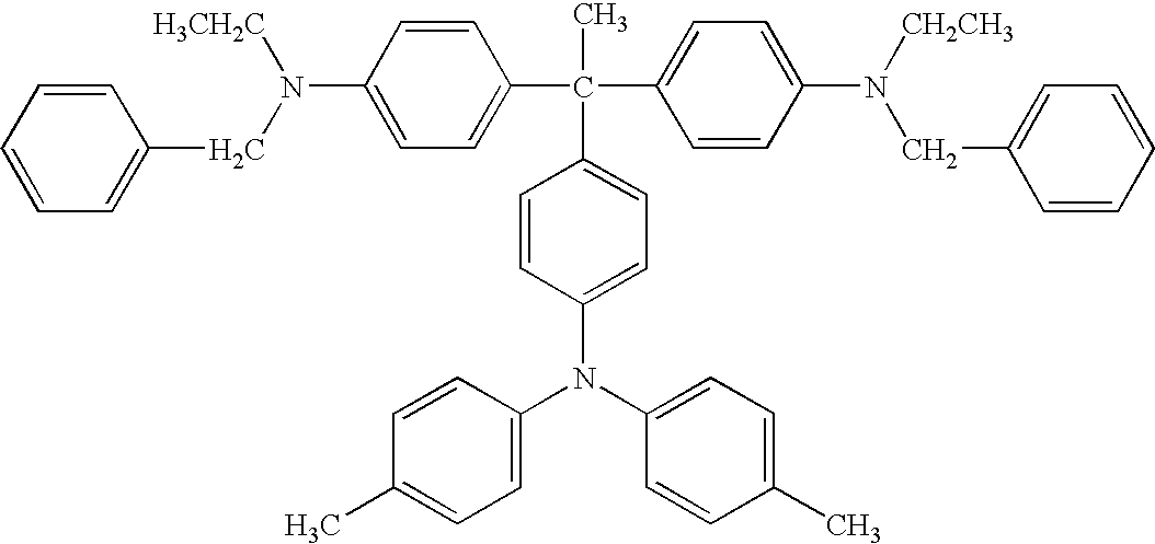
(6-7) -
TABLE 3 Formula No. 
(7-1) 
(7-2) 
(7-3) 
(7-4) 
(7-5) -
TABLE 4 Formula No. 
(8-1) 
(8-2) 
(8-3) 
(8-4) 
(8-5) - The compounds represented by the formulae (2) and (3) can reduce the likelihood or prevent the occurrence of image density unevenness. It is considered that the amino groups substituted with R9 and R10 can reduce the likelihood or prevent the oxidizing gas from producing a radical substance. Since the compounds represented by the formulae (2) and (3) have a charge transport structure, charges are not trapped therein, and therefore deterioration of electric property (such as increase of residual potential) hardly occurs.
-

- Each of R9 and R10 independently represents a substituted or unsubstituted aryl group or a substituted or unsubstituted alkyl group, R9 and R10 optionally share bond connectivity to form a heterocyclic group containing a nitrogen atom. Each of Ar1 and Ar2 independently represents a substituted or unsubstituted aryl group. Each of k and m independently represents an integer of from 0 to 3. Both of k and m does not simultaneously represent 0 and n represents an integer of from 1 to 3.
- Specific examples of the aryl groups represented by R9 and R10 include, but are not limited to, aromatic hydrocarbon groups derived from aromatic hydrocarbon rings, such as benzene, naphthalene, anthracene, and pyrene. Specific examples of the alkyl groups represented by R9 and R10 include, but are not limited to, methyl group, ethyl group, propyl group, butyl group, hexyl group, and undecanyl group. Among these, alkyl groups having 1 to 4 carbon atoms may be used. Specific examples of the aryl groups represented by Ar1 and Ar2 include, but are not limited to, aromatic hydrocarbon groups derived from aromatic hydrocarbon rings (e.g., benzene, naphthalene, anthracene, pyrene) having 1 to 4 valences; and aromatic heterocyclic groups derived from aromatic heterocyclic rings (e.g., pyridine, quinoline, thiophene, furan, oxazole, oxadiazole, carbazole) having 1 to 4 valences. Specific examples of the substituent groups thereof include, but are not limited to, alkyl groups (e.g., methyl group, ethyl group, propyl group, butyl group, hexyl group, undecanyl group), alkoxy groups (e.g., methoxy group, ethoxy group, propoxy group, butoxy group), halogen atoms (e.g., fluorine atom, chlorine atom, bromine atom, iodine atom), and aryl groups. Specific examples of the heterocyclic group containing a nitrogen atom formed of R9 and R10 include, but are not limited to, pyrrolidinyl group, piperidinyl group, pyrrolinyl group, and aromatic heterocyclic group derived from N-methyl carbazole, N-ethyl carbazole, N-phenyl carbazole, indole, and quinoline.
- Specific examples of suitable compounds represented by the formulae (2) and (3) include the following compounds shown in Tables 5 and 6, respectively, but are not limited thereto.
- The compounds represented by the formulae (2) and (3) further include compounds disclosed in published examined Japanese patent application No. (hereinafter referred to as JP-B) 58-57739 and JP 2529299. The compound represented by the formula (2) can be prepared by so-called Wittig reaction or Wittig-Horner reaction in which a triphenyl phosphonium salt or a phosphonic acid ester, respectively, is reacted with an aldehyde. The compound represented by the formula (3) can be prepared by reduction of the compound represented by the formula (2).
-
TABLE 5 Formula No. 
(2-1) 
(2-2) 
(2-3) 
(2-4) 
(2-5) 
(2-6) 
(2-7) 
(2-8) 
(2-9) 
(2-10) 
(2-11) 
(2-12) 
(2-13) 
(2-14) 
(2-15) -
TABLE 6 Formula No. 
(3-1) 
(3-2) 
(3-3) 
(3-4) 
(3-5) 
(3-6) 
(3-7) 
(3-8) 
(3-9) 
(3-10) 
(3-11) 
(3-12) 
(3-13) 
(3-14) 
(3-15) - Diamine compounds represented by the formula (4) are disclosed in JP-B 62-13382, and U.S. Pat. Nos. 4,223,144, 3,271,383, and 3,291,788 as an intermediate of a dye or a precursor of a polymer.
-

- Each of R11 and R12 independently represents a substituted or unsubstituted alkyl group or a substituted or unsubstituted aryl group. At least one of R11 and R12 is a substituted or unsubstituted aryl group. R11 and R12 optionally share bond connectivity to form a substituted or unsubstituted heterocyclic group containing a nitrogen atom. Ar3 represents a substituted or unsubstituted aryl group.
- When a photoreceptor includes such a compound, the resultant image quality is maintained in good level even after the photoreceptor is repeatedly used. The mechanism is considered as follows. Because an alkylamino group included in the compound has strong basic properties, an oxidizing gas and an ionic substance which are considered to cause image density unevenness can be neutralized thereby. Further, the diamine compound used for exemplary embodiments of the present invention has good charge transport ability because of having an amino group substituted with an aryl group, which is known as a functional group having good charge transport ability (described in a technical document “Guiding concept for developing better charge transporting organic materials”, Takahashi et al., Electrophotography (DENSHISHY ASHIN GAKKAISHI), Vol. 25, No. 3, p. 16 (1983)). In addition, when a photoreceptor includes the diamine compounds together with another charge transport material, the photoreceptor has better sensitivity and stability even after repeated use.
- The diamine compound represented by the formula (4) can be easily prepared by the method described in a technical document “A new synthesis of bisbenzils and novel poly(phenylquinoxaline)s therefrom”, E. Elce and A. S. Hay, Polymer, Vol. 37, No. 9, 1745 (1996). Specifically, a dihalogen compound represented by the following formula (12) is reacted with a secondary amine compound represented by the following formula (13) in the presence of a basic compound at a temperature of from room temperature to about 100° C.:
-
BH2C—Ar3CH2B (12) - Ar3 represents a substituted or unsubstituted aryl group and B represents a halogen atom.
-

- Each of R11 and R12 independently represents a substituted or unsubstituted alkyl group or a substituted or unsubstituted aryl group. At least one of R11 and R12 is a substituted or unsubstituted aryl group, and wherein R11 and R12 optionally share bond connectivity to form a substituted or unsubstituted heterocyclic group containing a nitrogen atom.
- Specific examples of the basic compounds include, but are not limited to, potassium carbonate, sodium carbonate, potassium hydroxide, sodium hydroxide, sodium hydride, sodium methylate, and potassium t-butoxide. Specific examples of the reaction solvents include, but are not limited to, dioxane, tetrahydrofuran, toluene, xylene, dimethyl sulfoxide, N,N-dimethyl formamide, N-methylpyrrolidone, 1,3-dimethyl-2-imidazolidinone, and acetonitrile.
- Specific examples of the alkyl groups represented by R11 and R12 included in the formulae (4) and (13) include, but are not limited to, methyl group, ethyl group, propyl group, butyl group, hexyl group, and undecanyl group. Specific examples of the aromatic group represented by R11, R12, and Ar3 included in the formulae (4) and (12) include, but are not limited to, aromatic hydrocarbon groups derived from aromatic hydrocarbon rings such as benzene, biphenyl, naphthalene, anthracene, fluorene, and pyrene; and aromatic heterocyclic groups derived from aromatic heterocyclic rings such as pyridine, quinoline, thiophene, furan, oxazole, oxadiazole, and carbazole. Specific examples of the substituent groups thereof include, but are not limited to, alkyl groups (e.g., methyl group, ethyl group, propyl group, butyl group, hexyl group, undecanyl group), alkoxy groups (e.g., methoxy group, ethoxy group, propoxy group, butoxy group), halogen atoms (e.g., fluorine atom, chlorine atom, bromine atom, iodine atom), aryl groups, and heterocyclic groups derived from heterocyclic rings such as pyrrolidine, piperidine, and piperazine. Specific examples of the heterocyclic group containing a nitrogen atom formed of R11 and R12 include, but are not limited to, condensed heterocyclic groups to which an aryl group is bound to heterocyclic groups, such as pyrrolidinyl group, piperidinyl group, and pyrrolinyl group.
- Specific preferred examples of suitable compounds represented by the formula (4) include the following compounds shown in Table 7, but are not limited thereto.
-
TABLE 7 Formula Ar3 R11 R12 No. 
—CH3 
(4-1) 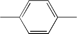
—CH2CH3 
(4-2) 
—CH3 
(4-3) 
—CH2CH3 
(4-4) 
—CH2CH2CH3 
(4-5) 
—CH2CH3 
(4-6) 


(4-7) 


(4-8) 


(4-9) 


(4-10) 
—CH2CH3 
(4-11) 
—CH2CH3 
(4-12) 


(4-13) 


(4-14) 
—CH2CH3 
(4-15) 
—CH3 
(4-16) 
—CH2CH3 
(4-17) 


(4-18) 
—CH3 
(4-19) 
—CH2CH3 
(4-20) 


(4-21) 


(4-22) 
—CH2CH3 
(4-23) 


(4-24) 
—CH2CH3 
(4-25) 
—CH3 
(4-26) 


(4-27) 
—CH2CH3 
(4-28) 
—CH3 (4-29) 
—CH2CH3 
(4-30) 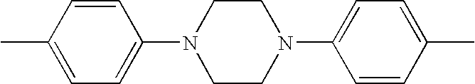
—CH2CH3 
(4-31) 
—CH2CH3 
(4-32) 
—CH2CH3 
(4-33) 


(4-34) 

(4-35) 

(4-36) 

(4-37) (*) —NR11R12 - The above-mentioned compounds (i.e., (A) an arylmethane compound having an alkylamino group; (B) a compound represented by the formula (2); (C) a compound represented by the formula (3); and (D) a compound represented by the formula (4)) can be added to either or both of the photosensitive layer and the outermost layer. When the photosensitive layer includes the charge generation layer and the charge transport layer, the above-mentioned compounds can be added to either or both thereof.
- The layer may include the compound in an amount of from 0.01 to 150% by weight based on total weight of the layer, but the amount is not limited thereto as long as the photoreceptor has good electric and mechanical properties. When the amount is too small, the resultant photoreceptor does not have sufficient oxidizing gas resistance. When the amount is too large, the resultant photoreceptor has sufficient oxidizing gas resistance, but does not have sufficient oxidizing gas resistance.
- The radical polymerizable compound having no charge transport structure for use in exemplary embodiments of the present invention is represented by the formula (1).
-

- Each of R1, R2, R3, R4, R5, and R6 independently represents a hydrogen atom or a group represented by the following formula:
-

- R7 represents a single bond, an alkylene group, an alkylene ether group, a polyoxyalkylene group, an alkylene ether group substituted with a hydroxyl group, an alkylene ether group substituted with a (meth)acryloyloxy group, an oxyalkylene carbonyl group, or a poly(oxyalkylene carbonyl) group; and R8 represents a hydrogen atom or a methyl group. Four or more of R1, R2, R3, R4, R5, and R6 do not simultaneously represent hydrogen atoms. R7 is preferably a single bond or an alkylene ether group substituted with a hydroxyl group.
- A compound having 5 or more acryloyloxy or methacryloyloxy groups as radical polymerizable functional groups may be used.
- A compound having 5 or more acryloyloxy groups can be prepared by subjecting a compound having 5 or more hydroxyl group and a member selected from an acrylic acid, an acrylate, an acrylic halide, and an acrylic ester to an esterification reaction or an interesterification reaction. A compound having 5 or more methacryloyloxy groups can be prepared in the same manner. Each of the 5 or more radial polymerizable groups may be the same or different.
- Specific examples of suitable combinations of R1, R2, R3, R4, R5, and R6 of the compound represented by the formula (1) include, but are not limited to, the following combinations:
- (a) 3 acryloyloxy groups and 3 hydrogen groups;
- (b) 4 acryloyloxy groups and 2 hydrogen groups;
- (c) 5 acryloyloxy groups and 1 hydrogen group;
- (d) 6 acryloyloxy groups;
- (e) 3 methacryloyloxy groups and 3 hydrogen groups;
- (f) 4 methacryloyloxy groups and 2 hydrogen groups;
- (g) 5 methacryloyloxy groups and 1 hydrogen group; and
- (h) 6 methacryloyloxy groups.
- In particular, specific examples of suitable compounds represented by the formula (1) include the following compounds shown in Table 8, but are not limited thereto.
-
TABLE 8 Formula No. 
(1-1) 
(1-2) 
(1-3) 
(1-4) 
(1-5) 
(1-6) 
(1-7) 
(1-8) 
(1-9) - These compounds can be used alone or in combination.
- These compounds can be prepared by esterification of polyols, and this method has high yield, low manufacturing cost, and high manufacturability. When 2 to 4 of the compounds are used in combination and a compound having 6 radical polymerizable functional groups is included therein, a mixture of a compound having 6 radical polymerizable functional groups which are esterified and a compound having 5 radical polymerizable functional groups and 1 hydrogen group which is unesterified may be used, because of high yield thereof. The mixture may include the compound having 6 radical polymerizable functional groups in an amount of from 20 to 99% by weight, more preferably from 30 to 97% by weight, and much more preferably from 40 to 95% by weight. When the compound having 5 radical polymerizable functional groups is used, the mixture may include the compound in an amount of from 20 to 99% by weight, more preferably from 30 to 97% by weight, and much more preferably from 40 to 95% by weight. When the compound having 4 radical polymerizable functional groups is used, the mixture may include the compound in an amount of from 0.01 to 30% by weight, more preferably from 0.1 to 20% by weight, and much more preferably from 3 to 5% by weight. When the compound having 3 radical polymerizable functional groups is used, the mixture may include the compound in an amount of from 0.01 to 30% by weight, more preferably from 0.1 to 20% by weight, and much more preferably from 3 to 5% by weight.
- Specific examples of the mixtures of the above compounds include, but are not limited to, the following mixtures.
- (a) A mixture of a compound having 6 acryloyloxy groups in an amount of from 30 to 70% by weight, and preferably from 40 to 60% by weight; and a compound having 5 acryloyloxy groups and 1 hydrogen group in an amount of from 30 to 70% by weight, and preferably from 40 to 60% by weight.
- (b) A mixture of a compound having 6 acryloyloxy groups in an amount of from 30 to 65% by weight, and preferably from 40 to 55% by weight; a compound having 5 acryloyloxy groups and 1 hydrogen group in an amount of from 30 to 65% by weight, and preferably from 40 to 55% by weight; and at least one compound selected from the following compounds (i) to (iv) in an amount of from 0.01 to 5% by weight, preferably from 1 to 3% by weight:
- (i) a compound having 1 acryloyloxy group and 5 hydrogen groups;
- (ii) a compound having 2 acryloyloxy groups and 4 hydrogen groups;
- (iii) a compound having 3 acryloyloxy groups and 3 hydrogen groups; and
- (iv) a compound having 4 acryloyloxy groups and 2 hydrogen groups.
- (c) A mixture of a compound having 6 methacryloyloxy groups in an amount of from 30 to 70% by weight, and preferably from 40 to 60% by weight; and a compound having 5 methacryloyloxy groups and 1 hydrogen group in an amount of from 30 to 70% by weight, and preferably from 40 to 60% by weight.
- (b) A mixture of a compound having 6 methacryloyloxy groups in an amount of from 30 to 65% by weight, and preferably from 40 to 55% by weight; a compound having 5 methacryloyloxy groups and 1 hydrogen group in an amount of from 30 to 65% by weight, and preferably from 40 to 55% by weight; and at least one compound selected from the following compounds (v) to (viii) in an amount of from 0.01 to 5% by weight, preferably from 1 to 3% by weight:
- (v) a compound having 1 methacryloyloxy group and 5 hydrogen groups;
- (vi) a compound having 2 methacryloyloxy groups and 4 hydrogen groups;
- (vii) a compound having 3 methacryloyloxy groups and 3 hydrogen groups; and
- (viii) a compound having 4 methacryloyloxy groups and 2 hydrogen groups.
- The outermost layer may include the radical polymerizable compound represented by the formula (1) in an amount of from 3 to 95% by weight, more preferably 5 to 80% by weight, and much more preferably from 10 to 70% by weight, based on total weight of the outermost layer. When the amount is not less than 3% by weight, three-dimensional cross-linking density of the outermost layer is too large, and therefore the resultant photoreceptor has dramatically better abrasion resistance compared to that using a related art thermoplastic resin. When the amount is not greater than 95% by weight, the outermost layer includes sufficient amount of the charge transport material, and therefore the electric property of the resultant photoreceptor hardly deteriorates.
- When the outermost layer is formed, a radical polymerizable monomer and/or oligomer having 1 to 4 functional groups can be used in combination in order to control the viscosity of the coating liquid, to maintain the smoothness of the outermost layer, to reduce the likelihood or prevent occurrence of crack caused due to the cross-linking contraction, and to decrease the surface free energy. When too large an amount of a radical polymerizable monomer and/or oligomer having 1 or 2 functional groups is used, there is a concern that mechanical durability of the outermost layer deteriorates. Therefore, a radical polymerizable monomer and/or oligomer having 3 or more functional groups may be used. Any related art radical polymerizable compounds can be used. The outermost layer may include the radical polymerizable monomer and/or oligomer having 1 to 4 functional groups in an amount of from 1 to 80% by weight, more preferably from 5 to 60% by weight, and much more preferably from 10 to 40% by weight, based on total weight of the outermost layer. When the radical polymerizable monomer and/or oligomer having 1 to 4 functional groups is used for controlling the viscosity of the coating liquid, the radical polymerizable monomer and/or oligomer may have a viscosity not greater than 1,000 mPa·s, and more preferably 800 mPa·s, at a temperature of 25° C.
- Specific examples of the radical polymerizable monomers having 1 to 4 functional groups include, but are not limited to, trimethylolpropane triacrylate (TMPTA), trimethylolpropane trimethacrylate, HPA modified trimethylolpropane triacrylate, EO modified trimethylolpropane triacrylate, PO modified trimethylolpropane triacrylate, caprolactone modified trimethylolpropane triacrylate, ECH modified trimethylolpropane triacrylate, HPA modified trimethylolpropane trimethacrylate, pentaerythritol triacrylate, pentaerythritol tetraacrylate (PEETA), glycerol triacrylate, ECH modified glycerol triacrylate, EO modified glycerol triacrylate, PO modified glycerol triacrylate, tris(acryloxyethyl)isocyanurate, alkyl modified dipentaerythritol tetraacrylate, alkyl modified dipentaerythritol triacrylate, dimethylolpropane tetraacrylate (DTMPTA), pentaerythritol ethoxy tetraacrylate, EO modified phosphoric acid triacrylate, 2,2,5,5-tetrahydroxymethylcyclopentanone tetraacrylate, 2-ethylhexyl acrylate, 2-hydroxyethyl acrylate, 2-hydroxypropyl acrylate, tetrahydrofurfuryl acrylate, 2-ethylhexylcarbitol acrylate, 3-methoxybutyl acrylate, benzyl acrylate, cyclohexyl acrylate, isoamyl acrylate, isobutyl acrylate, methoxy triethylene glycol acrylate, phenoxy tetraethylene glycol acrylate, cetyl acrylate, isostearyl acrylate, stearyl acrylate, styrene monomer, 1,3-butanediol diacrylate, 1,4-butanediol diacrylate, 1,4-butanediol dimethacrylate, 1,6-hexanediol diacrylate, 1,6-hexanediol dimethacrylate, diethylene glycol diacrylate, neopentyl glycol diacrylate, EO modified bisphenol A diacrylate, and EO modified bisphenol F diacrylate, neopentyl glycol diacrylate. Among these, trimethylolpropane triacrylate (TMPTA), HPA modified trimethylolpropane triacrylate, EO modified trimethylolpropane triacrylate, PO modified trimethylolpropane triacrylate, and ECH modified trimethylolpropane triacrylate may be used. (“EO” represents “ethyl eneoxy”, “PO” represents “propyleneoxy”, “ECH” represents “epichlorohydrin”, and “HPA” represents “alkylene”.)
- Specific examples of the radical polymerizable oligomers having 1 to 4 functional groups include, but are not limited to, epoxy acrylate oligomers, urethane acrylate oligomers, and polyester acrylate oligomers.
- The radical polymerizable compound having a charge transport structure for use in exemplary embodiments of the present invention has a positive hole transport structure (e.g., triarylamine, hydrazone, pyrazoline, carbazole) or an electron transport structure (e.g., condensed polycyclic quinone, diphenoquinone, electron-accepting aromatic rings having cyano group and nitro group); and a radical polymerizable functional group. The radical polymerizable functional group has a carbon-carbon double bond, and is not particularly limited.
- Specific examples of the radical polymerizable functional groups include, but are not limited to, 1-substituted ethylene group and 1,1-substituted ethylene group.
- The 1-substituted ethylene group can be represented by the following formula.
-
CH2═CH—X1— - X1 represents an arylene group (e.g., phenylene group, naphthylene group) which may have a substituent group, an alkenylene group which may have a substituent group, —CO—, —COO—, —CON(R20) (R20 represents a hydrogen atom; an alkyl group such as methyl group and ethyl group; an aralkyl group such as benzyl group, naphthylmethyl group, and phenethyl group; or an aryl group such as phenyl group and naphthyl group), or —S—.
- Specific examples of the 1-substituted ethylene groups include, but are not limited to, vinyl group, styryl group, 2-methyl-1,3-butadienyl group, vinyl carbonyl group, acryloyloxy group, acryloylamide group, and vinyl thioether group.
- The 1,1-substituted ethylene group can be represented by the following formula:
-
CH2═C(Y)—X2— - Y represents an alkyl group which may have a substituent group, an aralkyl group which may have a substituent group, a phenyl group which may have a substituent group, an aryl group (e.g., naphthyl group), a halogen atom, a cyano group, a nitro group, an alkoxy group (e.g., methoxy group, ethoxy group), —COOR21 (R21 represents a hydrogen atom; an alkyl group, such as methyl group and ethyl group, which may have a substituent group; an aralkyl group, such as benzyl group and phenethyl group, which may have a substituent group; or an aryl group, such as phenyl group and naphthyl group, which may have a substituent group), —CONR22R23 (each of R22 ad R23 independently represents a hydrogen atom; an alkyl group, such as methyl group and ethyl group, which may have a substituent group; an aralkyl group, such as benzyl group, naphthylmethyl group, and phenethyl group, which may have a substituent group; or an aryl group, such as phenyl group and naphthyl group, which may have a substituent group); and X1 represents the same group as X2, a single bond, or an alkylene group. At least one of Y and X2 is an oxycarbonyl group, a cyano group, an alkenylene group, or an aromatic ring.
- Specific examples of the 1,1-substituted ethylene groups include, but are not limited to, α-chlorinated acryloyloxy group, methacryloyloxy group, α-cyano ethylene group, α-cyano acryloyloxy group, α-cyano phenylene group, and methacryloylamino group.
- Specific examples of the substituent groups of X1, X2, and Y include, but are not limited to, a halogen atom, nitro group, cyano group, an alkyl group (e.g., methyl group, ethyl group), an alkoxy group (e.g., methoxy group, ethoxy group), an aryloxy group (e.g., phenoxy group), an aryl group (e.g., phenyl group, naphthyl group), and an aralkyl group (e.g., benzyl group, phenethyl group).
- Among the above-mentioned radical polymerizable functional groups, acryloyloxy group and methacryloyloxy group are effective. In order that the resultant photoreceptor has good electric property for a long term, the radical polymerizable compound may have one radical polymerizable functional group. When the radical polymerizable compound has 2 or more functional groups, the charge transport structure is bound to the cross-linking structure at plural sites and fixed therein, and thereby an intermediate structure (a cation radical) cannot be stably formed when the charge is transported. As a result, the charge tends to be trapped, and causes deterioration of sensitivity and increase of residual potential. In this case, the resultant image density tends to decrease, and the characters in the resultant image tend to be thinner.
- As the charge transport structure, a triarylamine structure is effective. When compounds represented by the following formulae (9) and (10) are used, the resultant photoreceptor has good sensitivity and electric property (such as residual potential) for a long term:
-

- R16 represents a hydrogen atom, a halogen atom, an alkyl group which may have a substituent group, an aralkyl group which may have a substituent group, an aryl group which may have a substituent group, a cyano group, a nitro group, an alkoxy group, —COOR17 (R17 represents a hydrogen atom, an alkyl group which may have a substituent group, an aralkyl group which may have a substituent group, or an aryl group which may have a substituent group), a halogenated carbonyl group, or —CONR18R19 (each of R18 and R19 independently represents a hydrogen atom, a halogen atom, an alkyl group which may have a substituent group, an aralkyl group which may have a substituent group, or an aryl group which may have a substituent group. Each of Ar9 and Ar10 independently represents a substituted or unsubstituted arylene group. Each of Ar11 and Ar12 independently represents a substituted or unsubstituted aryl group. X represents a single bond, a substituted or unsubstituted alkylene group, a substituted or unsubstituted cycloalkylene group, a substituted or unsubstituted alkylene ether group, an oxygen atom, a sulfur atom, or a vinylene group. Z represents a substituted or unsubstituted alkylene group, a substituted or unsubstituted alkylene ether group, or an alkyleneoxycarbonyl group. Each of j and k independently represents an integer of from 0 to 3.
- Specific examples of the alkyl groups represented by R16 include, but are not limited to, methyl group, ethyl group, propyl group, and butyl group. Specific examples of the aryl groups represented by R16 include, but are not limited to, phenyl group and naphthyl group. Specific examples of the aralkyl groups represented by R16 include, but are not limited to, benzyl group, phenethyl group, and naphthylmethyl group. Specific examples of the alkoxy groups represented by R16 include, but are not limited to, methoxy group, ethoxy group, and propoxy group. These groups may be substituted with a halogen atom, a nitro group, a cyano group, an alkyl group (e.g., methyl group, ethyl group), an alkoxy group (e.g., methoxy group, ethoxy group), an aryloxy group (e.g., phenoxy group), an aryl group (e.g., phenyl group, naphthyl group), an aralkyl group (e.g., benzyl group, phenethyl group), etc.
- Among the above groups represented by R16, a hydrogen atom and a methyl group may be used.
- Each of Ar11 and Ar12 independently represents a substituted or unsubstituted aryl group. Specific examples of the aryl groups include, but are not limited to, condensed polycyclic hydrocarbon groups, uncondensed cyclic hydrocarbon groups, and heterocyclic groups.
- The condensed polycyclic hydrocarbon group may include a ring having 18 or less carbon atoms. Specific examples of such condensed polycyclic hydrocarbon groups include, but are not limited to, pentanyl group, indenyl group, naphthyl group, azulenyl group, heptalenyl group, biphenylenyl group, as-indacenyl group, s-indacenyl group, fluorenyl group, acenaphthylenyl group, pleiadenyl group, acenaphthenyl group, phenalenyl group, phenanthryl group, anthryl group, fluoranthenyl group, acephenanthrylenyl group, aceanthrylenyl group, triphenylenyl group, pyrenyl group, chrysenyl group, and naphthacenyl group.
- Specific examples of the uncondensed cyclic hydrocarbon groups include, but are not limited to, monovalent groups derived from benzene, diphenyl ether, polyethylene diphenyl ether, diphenyl thioether, diphenyl sulfone, biphenyl, polyphenyl, diphenyl alkane, diphenyl alkene, diphenyl alkyne, triphenylmethane, distyrylbenzene, 1,1-diphenyl cycloalkane, polyphenyl alkane, and polyphenyl alkene. In addition, monovalent groups derived from polycyclic hydrocarbons such as 9,9-diphenyl fluorene can also be used.
- Specific examples of the heterocyclic groups include, but are not limited to, monovalent groups derived from carbazole, dibenzofuran, dibenzothiophene, oxadiazole, thiazole, etc.
- The aryl groups represented by Ar11 and Ar12 may have the following substituent groups.
- (1) A halogen atom, a cyano group, a nitro group, etc.
- (2) A straight-chain or branched-chain alkyl group having 1 to 12 carbon atoms, more preferably 1 to 8 carbon atoms, and much more preferably 1 to 4 carbon atoms, which may substituted with a fluorine atom; a hydroxyl group; a cyano group; an alkoxy group having 1 to 4 carbon atoms; or a phenyl group substituted with a halogen atom, an alkyl group having 1 to 4 carbon atoms, or an alkoxy group having 1 to 4 carbon atoms. Specific examples of the alkyl groups include, but are not limited to, methyl group, ethyl group, n-butyl group, i-propyl group, t-butyl group, s-butyl group, n-propyl group, trifluoromethyl group, 2-hydroxyethyl group, 2-ethoxyethyl group, 2-cyanoethyl group, 2-methoxyethyl group, benzyl group, 4-chlorobenzyl group, 4-methylbenzyl group, and 4-phenylbenzyl group.
- (3) An alkoxy group (—OR30, wherein R30 represents an alkyl group defined in the above paragraph (2)). Specific examples of the alkoxy groups include, but are not limited to, methoxy group, ethoxy group, n-propoxy group, i-propoxy group, t-butoxy group, n-butoxy group, s-butoxy group, i-butoxy group, 2-hydroxyethoxy group, benzyloxy group, and trifluoromethoxy group.
- (4) An aryloxy group. Specific examples of aryl groups include, but are not limited to, phenyl group and naphthyl group. The aryloxy group may substituted with an alkoxy group having 1 to 4 carbon atoms, an alkyl group having 1 to 4 carbon atoms, or a halogen atom. Specific examples of the aryloxy groups include, but are not limited to, phenoxy group, 1-naphthyloxy group, 2-naphthyloxy group, 4-methoxyphenoxy group, and 4-methylphenoxy group.
- (5) An alkylmercapto group or an arylmercapto group. Specific examples of these groups include, but are not limited to, methylthio group, ethylthio group, phenylthio group, and p-methylphenylthio group.
- (6) A substituent group represented by the following formula:
-

- wherein each of Rd and Re independently represents a hydrogen atom, an alkyl group defined in the above paragraph (2), or an aryl group (e.g., phenyl group, biphenyl group, naphthyl group) which may substituted with an alkoxy group having 1 to 4 carbon atoms, an alkyl group having 1 to 4 carbon atoms, or a halogen atom; and wherein Rd and Re optionally share bond connectivity to form a ring. Specific examples of the above substituent groups include, but are not limited to, amino group, diethylamino group, N-methyl-N-phenylamino group, N,N-diphenylamino group, N,N-di(tolyl)amino group, dibenzylamino group, piperidino group, morpholino group, and pyrrolidino group.
- (7) An alkylenedioxy group and an alkylenedithio group such as methylenedioxy group and methylenedithio group.
- (8) A substituted or unsubstituted styryl group, a substituted or unsubstituted β-phenyl styryl group, diphenyl aminophenyl group, dinitrile aminophenyl group, etc.
- Specific examples of the arylene groups represented by Ar9 and Ar1− include, but are not limited to, divalent groups derived from the aryl groups represented by Ar11 and Ar12.
- X represents a single bond, a substituted or unsubstituted alkylene group, a substituted or unsubstituted cycloalkylene group, a substituted or unsubstituted alkylene ether group, an oxygen atom, a sulfur atom, or a vinylene group.
- The substituted or unsubstituted alkylene group is a straight-chained or branched-chain alkylene group having 1 to 12 carbon atoms, preferably 1 to 8 carbon atoms, and more preferably 1 to 4 carbon atoms. These alkylene groups may have a fluorine atom, a hydroxyl group, a cyano group, an alkoxy group having 1 to 4 carbon atoms, a phenyl group, or a phenyl group substituted with a halogen atom, an alkyl group having 1 to 4 carbon atoms, or an alkoxy group having 1 to 4 carbon atoms. Specific examples of the substituted or unsubstituted alkylene groups include, but are not limited to, methylene group, ethylene group, n-butylene group, i-propylene group, t-butylene group, s-butylene group, n-propylene group, trifluoromethylene group, 2-hydroxyethylene group, 2-ethoxyethylene group, 2-cyanoethylene group, 2-mehoxyethylene group, benzylidene group, phenylethylene group, 4-chlorophenylethylene group, 4-methylphenylethylene group, and 4-biphenylethylene group.
- The substituted or unsubstituted cycloalkylene group is a cyclic alkylene group having 5 to 7 carbon atoms which may have a fluorine atom, a hydroxyl group, an alkyl group having 1 to 4 carbon atoms, or an alkoxy group having 1 to 4 carbon atoms. Specific examples of the substituted or unsubstituted cycloalkylene groups include, but are not limited to, cyclohexylidene group, cyclohexylene group, and 3,3-dimethylcyclohexylidene group.
- Specific examples of the substituted or unsubstituted alkylene ether groups include, but are not limited to, an alkyleneoxy group (e.g., ethyleneoxy group, propyleneoxy group); an alkylenedioxy group derived from ethylene glycol, propylene glycol, etc.; and di- or poly(oxyalkylene)oxy group derived from diethylene glycol, tetraethylene glycol, tripropylene glycol. The alkylene group of the alkylene ether group may have a substituent group, such as a hydroxyl group, a methyl group, and an ethyl group.
- Specific examples of the vinylene groups include, but are not limited to, the following substituent groups:
-
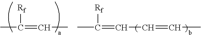
- Rf represents a hydrogen atom, an alkyl group (defined in the above paragraph (2)), or an aryl group (the same aryl groups represented by Ar11 and Ar12); a represents an integer of 1 or 2; and b represents an integer of from 1 to 3.
- Z represents a substituted or unsubstituted alkylene group, a substituted or unsubstituted alkylene ether group, or an alkyleneoxycarbonyl group.
- Specific examples of the substituted or unsubstituted alkylene groups include, but are not limited to, the same alkylene groups represented by X.
- Specific examples of the substituted or unsubstituted alkylene ether groups include, but are not limited to, the same alkylene ether groups represented by X.
- Specific examples of the alkyleneoxycarbonyl groups include, but are not limited to, caprolactone modified groups.
- As the monofunctional radical polymerizable compound having a charge transport structure, a compound represented by the following formula (11) may be used:
-

- Each of r, p, and q independently represents an integer of 0 or 1. Each of s and t independently represents an integer of from 0 to 3. Ra represents a hydrogen atom or a methyl group. Each of Rb and Rc independently represents an alkyl group having 1 to 6 carbon atoms. Za represents a single bond, a methylene group, an ethylene group,
-

- Among these compounds represented by the formula (11), compounds in which each of Rb and Rc independently represents a methyl group or an ethyl group may be used.
- Each of the monofunctional radical polymerizable compounds having a charge transport structure represented by the formulae (9), (10), and (11) has a carbon-carbon double bond on its end. Since this carbon-carbon double bond opens when polymerized with the radical polymerizable compound having no charge transport structure represented by the formula (1), the monofunctional radical polymerizable compound having a charge transport structure hardly becomes the end of the resultant polymer. In other words, the monofunctional radical polymerizable compound having a charge transport structure is present in the main chain of the resultant polymer formed by reacting with the radical polymerizable compound having no charge transport structure represented by the formula (1), and further present in the cross-linking chain which connects each of the main chains. (The cross-linking chain includes an intermolecular cross-linking chain which connects a polymer with another polymer, and an intramolecular cross-linking chain which connects a folded portion of the main chain of a polymer with another portion of the main chain of the polymer located far from the folded portion.) Since the triarylamine structure of the monofunctional radical polymerizable compound is suspended from the main chain or the cross-linking chain through the intermediary of a functional group, such as carbonyl group, the triarylamine structure can flexibly take various configurations, even though the triarylamine structure is bulky because of having at least 3 aryl groups radially bound to the nitrogen atom. As a result, each of the triarylamine structures can be arranged to be adjacent to each other while taking a reasonable distance therebetween in the molecular, and the molecular has a little structural strain. When the resultant polymer is used for the outermost layer of a photoreceptor, it seems that the charge transport path is hardly broken off.
- Specific examples of suitable monofunctional radical polymerizable compounds having a charge transport structure include the following compounds shown in Table 9, but are not limited thereto.
-
TABLE 9 Formula/No. 


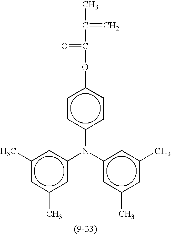


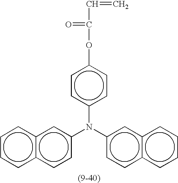


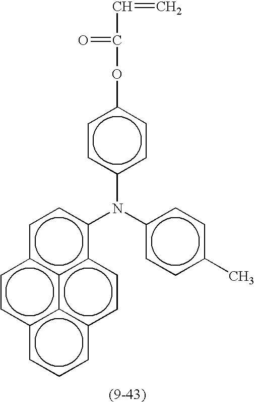


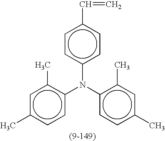


- The outermost layer of the photoreceptor of exemplary embodiments of the present invention may include the monofunctional radical polymerizable compound in an amount of from 20 to 80% by weight, and preferably from 30 to 70% by weight, based on total weight of the outermost layer. When the amount is too small, the outermost layer has insufficient charge transport ability, and therefore electrical properties thereof deteriorate and deterioration of sensitivity after repeated use and increase of residual potential are caused. When the amount is too large, the outermost layer includes too small a quantity of the radical polymerizable compound having no charge transport structure represented by the formula (1). Therefore cross-linking density thereof decreases, resulting in deterioration of abrasion resistance. The optimal amount depends on the electrophotographic process in which the resultant photoreceptor used but when the amount is from 30 to 70% by weight, the resultant photoreceptor generally has both good electric property and good abrasion resistance.
- The outermost layer of the photoreceptor of exemplary embodiments of the present invention include a cured product formed by subjecting the radical polymerizable compound having no charge transport structure represented by the formula (1) and the radical polymerizable compound (for example, monofunctional) having a charge transport structure to a cross-linking reaction, upon application of at least one member selected from heat, light, and ionizing radiation. When the cross-linking reaction is performed upon application of heat or light, a polymerization initiator can be used to efficiently proceed the reaction. When the cross-linking reaction is performed upon application of ionizing radiation, a polymerization initiator is not necessarily used. However, a polymerization initiator can be used when the residual unreacted components are subjected to a cross-linking reaction upon application of heat or light in the succeeding process.
- Specific examples of heat polymerization initiators include, but are not limited to, peroxide initiators (e.g., 2,5-dimethylhexane-2,5-dihydroperoxide, dicumyl peroxide, benzoyl peroxide, t-butyl cumyl peroxide, 2,5-dimethyl-2,5-di(peroxybenzoyl)hexyne-3, di-t-butyl peroxide, t-butyl hydroperoxide, cumene hydroperoxide, lauroyl peroxide), and azo initiators (e.g., azobis isobutyl nitrile, azobis cyclohexane carbonitrile, azobis methyl isobutyrate, azobis isobutyl amidine hydrochloride, 4,4′-azobis-4-cyano valeric acid).
- Specific examples of photo polymerization initiators include, but are not limited to, acetophenone or ketal initiators (e.g., diethoxy acetophenone, 2,2-dimethoxy-1,2-diphenylethane-1-one, 1-hydroxy-cyclohexyl-phenyl-ketone, 4-(2-hydroxyethoxy)phenyl-(2-hydroxy-2-propyl)ketone, 2-benzyl-2-dimethylamino-1-(4-morpholinophenyl)butanone-1,2-hydroxy-2-methyl-1-phenylpropane-1-one, 2-methy-2-morpholino(4-methylthiophenyl)propane-1-one, 1-phenyl-1,2-propanedione-2-(o-ethoxycarbonyl)oxime); benzoin ether initiators (e.g., benzoin, benzoin methyl ether, benzoin ethyl ether, benzoin isobutyl ether, benzoin isopropyl ether); benzophenone initiators (e.g., benzophenone, 4-hydroxy benzophenone, methyl o-benzoyl benzoate, 2-benzoyl naphthalene, 4-benzoyl biphenyl, 4-benzoyl phenyl ether, acrylic benzophenone, 1,4-benzoyl benzene); thioxanthone initiators (e.g., 2-isopropyl thioxanthone, 2-chloro thioxanthone, 2,4-dimethyl thioxanthone, 2,4-diethyl thioxanthone, 2,4-dichloro thioxanthone); titanocene initiators (e.g., bis(cyclopentadienyl)-di-chloro-titanium, bis(cyclopentadienyl)-di-phenyl-titanium, bis(cyclopentadienyl)-bis(2,3,4,5,6-pentafluorophenyl)-titanium, bis(cyclopentadienyl)-bis(2,6-difluoro-3-(pyrrol-1-yl)phenyl)-titanium); and ethyl anthraquinone, 2,4,6-trimethylbenzoyl diphenylphosphine oxide, 2,4,6-trimethylbenzoyl phenylethoxyphosphine oxide, bis(2,4,6-trimethylbenzoyl)phenylphosphine oxide, bis(2,4-dimethoxybenzoyl)-2,4,4-trimethylpentylphosohine oxide, methylphenyl glyoxylate, 9,10-phenanthrene, acridine compounds, triazine compounds, and imidazole compounds.
- Photo polymerization accelerators, such as triethanolamine, methyl diethanolamine, ethyl 4-dimethylamino benzoate, isoamyl 4-dimethylamino benzoate, (2-dimethylamino)ethyl benzoate, and 4,4′-dimethylamino benzophenone, can be used in combination with the above photo polymerization initiators.
- These polymerization initiators can be used alone or in combination. The content of the polymerization initiator is 0.5 to 40 parts by weight, preferably 1 to 20 parts by weight, based on 100 parts by weight of the radical polymerizable compounds.
- The outermost layer of the photoreceptor of an exemplary embodiment of the present invention may optionally include a particulate filler so as to enhance abrasion resistance thereof.
- The filler may have an average primary particle diameter of from 0.01 to 0.5 μm in terms of enhancing transmittance and abrasion resistance of the outermost layer. When the average primary particle diameter is too small, the filler cannot be well dispersed, and therefore abrasion resistance cannot be enhanced. When the average primary particle diameter is too large, the filler particles tend to settle down in the dispersion thereof, and toner films tend to be formed on the resultant layer.
- As the content of the filler increases, abrasion resistance thereof increases. However, when the content is too large, residual potential tends to increase and transmittance decreases. The outermost layer typically includes the filler in an amount not greater than 50% by weight, and preferably not greater than 30% by weight.
- Further, the filler is may be surface-treated with at least one surface treatment agent to enhance dispersibility thereof. When the filler is not well dispersed, residual potential increases, transmittance of the layer decreases, the layer cannot be uniformly coated, and abrasion resistance deteriorates. Any related art surface treatment agents can be used including a surface treatment agent which can keep insulation of the filler.
- The content of the surface treatment agent depends on the average primary diameter of the filler used but is typically from 3 to 30% by weight, and preferably from 5 to 20% by weight, based on total weight of the filler. When the content is too small, the filler cannot be well dispersed. When the content is too large, residual potential extremely increases.
- Of course, plural fillers can be used in combination.
- The coating liquid of the outermost layer may optionally include other additives, such as a plasticizer (for the purpose of stress relaxation and enhancement of adhesiveness), a leveling agent, a non-radical polymerizable low-molecular-weight charge transport material, etc. Any related art additives can be used, and are not particularly limited. Specific examples of the plasticizers include, but are not limited to, dibutyl phthalate and dioctyl phthalate. The coating liquid typically includes the plasticizer in an amount not greater than 20 parts by weight, and preferably not greater than 10 parts by weight, based on 100 parts by weight of the solid content of the coating liquid. Specific examples of the leveling agents include, but are not limited to, silicone oils (e.g., dimethyl silicone oil, methyl phenyl silicone oil), polymers and oligomers having a side chain including a perfluoroalkyl group. The coating liquid may include the leveling agent in an amount not greater than 3 parts by weight, based on total weight of the solid content of the coating liquid.
- The outermost layer of the photoreceptor of an exemplary embodiment of the present invention is formed by applying a coating liquid including a radical polymerizable compound having no charge transport structure represented by the formula (1) and a radical polymerizable compound (for example monofunctional) having a charge transport structure on the photosensitive layer (to be described later), and then subjecting to curing. When the radical polymerizable compounds are liquid, other components are dissolved therein and the solution can be used as the coating liquid as it is. Typically, the components are dissolved in a solvent to prepare the coating liquid. Any related art solvents can be used, and are not particularly limited. Specific examples of the solvents include, but are not limited to, alcohols (e.g., methanol, ethanol, propanol, butanol), ketones (e.g., acetone, methyl ethyl ketone, methyl isobutyl ketone, cyclohexanone), esters (e.g., ethyl acetate, butyl acetate), ethers (e.g., tetrahydrofuran, dioxane, propyl ether), halogenated solvents (e.g., dichloromethane, dichloroethane, trichloroethane, chlorobenzene), aromatic solvents (e.g., benzene, toluene, xylene), and cellosolves (e.g., methyl cellosolve, ethyl cellosolve, cellosolve acetate). These solvents can be used alone or in combination.
- The outermost layer can be formed by any known coating methods, and are not particularly limited. A suitable solvent can be selected according to the viscosity of a coating liquid, a targeted thickness of the layer, etc. Specific examples of the coating methods include, but are not limited to, a dip coating method, a spray coating method, a bead coating method, and a ring coating method.
- In exemplary embodiments of the present invention, the applied coating liquid is subjected to curing (i.e., cross-linking) by applying energy thereto to form a cured outermost layer. As the applying energy, heat energy, light energy, and ionizing radiation energy can be used. Since the ionizing radiation energy is deeply infiltrate and has strong intensity, the constituent materials of the photoreceptor tends to be deteriorated and therefore electrophotographic property thereof deteriorates. For this reason, heat energy and light energy may be used. When the light energy is used, the amount of a solvent used in manufacturing process and the amount of energy used for curing can be decreased. In addition, the strength of the resultant layer increases. These energies can be used alone or in combination.
- As the heat energy, gases such as air and nitrogen, heat media, infrared ray, electromagnetic wave, etc., are heated and then applied to the coated surface or the backside thereof. The heating temperature may be not less than 100° C. and not greater than 170° C. When the heating temperature is too low, the reaction rate is too slow, and therefore productivity decreases. Further, unreacted materials tend to remain in the resultant layer. When the heating temperature is too high, the resultant layer largely contracts when cross-linked, and may come to resemble an orange peel. Cracking may appear on the layer and the layer tends to peel off from the adjacent layer. If volatile components present in the photosensitive layer are sprayed, electric property of the resultant photoreceptor deteriorates. When a resin which largely contracts when cross-linked is used, the resin may be pre-cross-linked at a low temperature of less than 100° C., and then finally cross-linked at a high temperature of not less than 100° C.
- As the light energy, light sources, such as ultrahigh pressure mercury lamp, high pressure mercury lamp, low pressure mercury lamp, carbon-arc lamp, and xenon-arc metal halide lamp can be used. The light source may be selected considering the light absorption properties of the radical polymerizable compound having no charge transport structure, the radical polymerizable compound (for example monofunctional) having a charge transport structure, and a polymerization initiator used. The light source may emit a light with an illuminance of from 50 to 2,000 W/cm2 at a wavelength of 365 nm. The light source may emit a light with an illuminance mentioned above at the maximum wavelength. When the illuminance is too small, it takes too long a time for the curing, resulting in decreasing of productivity. When the illuminance is too large, the resultant layer largely contracts when cross-linked, and may come to resemble an orange peel. Cracking may appear on the layer and the layer tends to peel off from the adjacent layer.
- The ionizing radiation is a radiation which can ionize a substance. Specific examples of the ionizing radiations include direct ionizing radiations, such as alpha ray and electron ray, and indirect ionizing radiations, such as X-ray and neutron ray. Any related art ionizing radiations can be used for the present invention but an electron ray may be used considering effects on the human body. Specific examples of electron ray irradiation devices include, but are not limited to, electron ray accelerators, such as Cockcroft-Walton accelerator, Van de Graff accelerator, resonance transformer accelerator, insulated core transformer accelerator, linear accelerator, Dynamitron accelerator, and high-frequency accelerator.
- The electron ray irradiation device may irradiate an electron having an energy level of from 100 to 1,000 keV, preferably from 100 to 300 keV, at an irradiation dose of from 0.1 to 30 Mrad. When the irradiation dose is too small, the electron ray cannot reach inside of the outermost layer, and therefore deep portion of the layer cannot be sufficiently cross-linked. When the irradiation dose is too large, the electron ray may reach to the charge transport layer and the charge generation layer (to be mentioned later) and deteriorates the constituent materials thereof.
- When the ionizing radiation is irradiated, heat ray is generated from the irradiation device, and thereby the surface temperature of the photoreceptor increases. When the surface temperature is too high, the outermost layer tends to largely contract and low-molecular-weight components present in the adjacent layer tend to move to the outermost layer, resulting in inhibition of the curing and deterioration of electric property of the photoreceptor. When the ionizing radiation is irradiated, the surface of the photoreceptor typically has a temperature not greater than 100° C., and preferably not greater than 80° C. If the surface needs to be cooled, the inside of the photoreceptor can be cooled using a cooling agent, or cooled gas or liquid.
- The cured outermost layer is optionally heated after the curing. For example, when a large amount of residual solvent is present in the layer, the residual solvent may be volatilized and removed upon application of heat so as to reduce the likelihood or prevent deterioration of the electrical properties of the photoreceptor.
- The outermost layer may have a thickness of from 1 to 15 μm, and more preferably from 3 to 10 μm, from the viewpoint of protecting the photosensitive layer. When the outermost layer is too thin, the photosensitive layer cannot be protected from mechanical abrasion made by contacting members and contact discharge performed by a charger. In addition, the layer is hardly leveled and may come to resemble an orange peel. When the outermost layer is too thick, charges tend to diffuse, and thereby the resultant image reproducibility decreases.
- An adhesion layer is optionally formed between the outermost layer and the photosensitive layer for the purpose of reducing the likelihood or preventing the layers from peeing off from each other.
- The adhesion layer can be formed using the above-mentioned radical polymerizable compounds, non-cross-linked polymer compounds, etc. Specific examples of the non-cross-linked polymers include, but are not limited to, polyamides, polyurethanes, epoxy resins, polyketones, polycarbonates, silicone resins, acrylic resins, polyvinyl butyrals, polyvinyl formals, polyvinyl ketones, polystyrenes, poly-N-vinylcarbazoles, polyacrylamides, polyvinyl benzals, polyesters, phenoxy resins, vinyl chloride-vinyl acetate copolymers, polyvinyl acetates, polyphenylene oxides, polyvinyl pyridines, cellulose resins, casein, polyvinyl alcohols, polyvinyl pyrrolidones. Each of these non-cross-linked polymer compounds and the radical polymerizable compounds can be used alone or in combination, respectively. Of course, a non-cross-linked polymer compound and a radical polymerizable compound can be used in combination as long as there is good adhesiveness. The charge transport materials used for the exemplary embodiments of the present invention can also be used in combination. In addition, any additives enhancing adhesiveness can be used in combination.
- The adhesion layer is formed by applying a coating liquid in which the layer components are dissolved or dispersed in a solvent, such as tetrahydrofuran, dioxane, dichloroethane, and cyclohexane, using a coating method, such as a dip coating method, a spray coating method, a bead coating method, and a ring coating method. The adhesion layer typically has a thickness of from 0.1 to 5 μm, and preferably from 0.1 to 3 μm.
- As mentioned above, the photosensitive layer may be either multi-layered or single-layered. A multi-layered photosensitive layer typically includes a charge generation layer and a charge transport layer. A single-layered photosensitive layer typically has both charge generation ability and charge transport ability. These photosensitive layers will be explained in detail.
- The charge generation layer includes a charge generation material having a function of generating a charge as a main component, and optionally includes a binder resin in combination. As the charge generation material, inorganic materials and organic materials can be used.
- Specific examples of the inorganic materials include, but are not limited to, crystalline selenium, amorphous selenium, selenium-tellurium compounds, selenium-tellurium-halogen compounds, and amorphous silicon. Specifically, amorphous silicon in which dangling bonds are terminated with a hydrogen atom or a halogen atom, and that doped with a boron atom or a phosphorous atom may be used.
- Specific examples of the organic materials include, but are not limited to, phthalocyanine pigments (e.g., metal phthalocyanine, metal-free phthalocyanine), azulenium salt pigments, squaric acid methyne pigments, azo pigments having a carbazole skeleton, azo pigments having a triarylamine skeleton, azo pigments having a diphenylamine skeleton, azo pigments having a dibenzothiophene skeleton, azo pigments having a fluorenone skeleton, azo pigments having an oxadiazole skeleton, azo pigments having a bisstilbene skeleton, azo pigments having a distyryloxadiazole skeleton, azo pigments having a distyrylcarbazole skeleton, perylene pigments, anthraquinone and polycyclic quinone pigments, quinonimine pigments, diphenylmethane and triphenylmethane pigments, benzoquinone and naphthoquinone pigments, cyanine and azomethine pigments, indigoid pigments, bisbenzimidazole pigments, etc. These charge generation materials can be used alone or in combination.
- Specific examples of the binder resins include, but are not limited to, polyamides, polyurethanes, epoxy resins, polyketones, polycarbonates, silicone resins, acrylic resins, polyvinyl butyrals, polyvinyl formals, polyvinyl ketones, polystyrenes, poly-N-vinylcarbazoles, polyacrylamides, polyvinyl benzals, polyesters, phenoxy resins, vinyl chloride-vinyl acetate copolymers, polyvinyl acetates, polyphenylene oxides, polyvinyl pyridines, cellulose resins, casein, polyvinyl alcohols, and polyvinyl pyrrolidones. These binder resins can be used alone or in combination. The charge generation layer may include the binder resin in an amount of from 0 to 500 parts by weight, and more preferably from 10 to 300 parts by weight, based on 100 parts by weight of the charge generation material.
- The charge generation layer is typically formed by a vacuum thin layer manufacturing method or a casting method using a liquid dispersion. Specific examples of the vacuum thin layer manufacturing methods include, but are not limited to, a vacuum deposition method, a glow discharge polymerization method, an ion plating method, a sputtering method, a reactive sputtering method, and a CVD method. The vacuum thin layer manufacturing method can well form a layer of the above inorganic and organic charge generation materials. When the charge generation layer is formed by a casting method, a dispersion in which the above inorganic or organic charge generation material, optionally together with the binder resin, are dispersed in a solvent, such as tetrahydrofuran, dioxane, dioxolane, toluene, dichloromethane, monochlorobenzene, dichloroethane, cyclohexanone, cyclopentanone, anisole, xylene, methyl ethyl ketone, acetone, ethyl acetate, and butyl acetate, using a ball mill, an attriter, a sand mill, a bead mill, etc. is diluted as appropriate and then applied. The dispersion optionally includes a leveling agent, such as dimethyl silicone oil, methylphenyl silicone oil. Specific examples of the casting methods include any known coating methods, such as a dip coating method, a spray coating method, a bead coating method, and a ring coating method.
- The charge generation layer typically has a thickness of from 0.01 to 5 μm, and preferably from 0.05 to 2 μm.
- The charge transport layer has a function of transporting a charge, and includes a charge transport material and a binder resin as main components.
- As the charge transport materials, electron transport materials and positive-hole transport materials can be used.
- Specific examples of the electron transport materials include, but are not limited to, electron accepting materials, such as chloranil, bromanil, tetracyanoethylene, tetracyanoquinodimethane, 2,4,7-trinitro-9-fluorenone, 2,4,5,7-tetranitro-9-fluorenone, 2,4,5,7-tetranitroxanthone, 2,4,8-trinitrothioxanthone, 2,6,8-trinitro-4H-indeno[1,2-b]thiophene-4-one, and 1,3,7-trinitrodibenzothiophene-5,5-dioxide. These can be used alone or in combination.
- Specific examples of the positive-hole transport materials include, but are not limited to, poly-N-vinylcarbazoles and derivatives thereof, poly-γcarbazolylethyl glutamate and derivatives thereof, condensates of pyrene and formaldehyde and derivatives thereof, polyvinyl pyrene, polyvinyl phenanthrene, polysilane, oxazole derivatives, oxadiazole derivatives, imidazole derivatives, monoarylamine derivatives, diarylamine derivatives, triarylamine derivatives, stilbene derivatives, α-phenylstilbene derivatives, benzidine derivatives, diarylmethane derivatives, triarylmethane derivatives, 9-styrylanthracene derivatives, pyrazoline derivatives, divinylbenzene derivatives, hydrazone derivatives, indene derivatives, butadiene derivatives, pyrene derivatives, bisstilbene derivatives, and enamine derivatives. These can be used alone or in combination.
- Specific examples of the binder resins include, but are not limited to, thermoplastic and thermosetting resins, such as polystyrenes, styrene-acrylonitrile copolymers, styrene-butadiene copolymers, styrene-maleic anhydride copolymers, polyesters, polyvinyl chlorides, vinyl chloride-vinyl acetate copolymers, polyvinyl acetates, polyvinyl chlorides, polyarylate resins, phenoxy resins, polycarbonates, cellulose acetate resins, ethylcellulose resins, polyvinyl butyrals, polyvinyl formals, polyvinyl toluenes, poly-N-vinylcarbazoles, acrylic resins, silicone resins, epoxy resins, melamine resins, urethane resins, phenol resins, and alkyd resins. In addition, polymeric charge transport materials, such as polycarbonates polyesters, polyurethanes, polyethers, polysiloxanes, and acrylic resins having an arylamine skeleton, a benzidine skeleton, a hydrazone skeleton, a carbazole skeleton, a stilbene skeleton, or a pyrazoline skeleton; and polymeric materials having a polysilane skeleton can be used.
- The charge transport layer preferably includes the charge transport material in an amount of from 20 to 300 parts by weight, and more preferably 40 to 150 parts by weight, based on 100 parts by weight of the binder resin. The polymeric charge transport material can be used alone or in combination with the binder resin.
- Specific examples of the solvents used for the charge transport layer coating liquid include, but are not limited to, tetrahydrofuran, dioxane, toluene, dichloromethane, monochlorobenzene, dichloroethane, cyclohexanone, methyl ethyl ketone, and acetone. These solvents can be used alone or in combination.
- A plasticizer and/or a leveling agent may be optionally added to the charge transport layer. Specific examples of the plasticizers include, but are not limited to, typical plasticizers used for general resins, such as dibutyl phthalate and dioctyl phthalate. The charge transport layer preferably includes the plasticizer in an amount of from 0 to 30 parts by weight, based on 100 parts by weight of the binder resin. Specific examples of the leveling agents include, but are not limited to, silicone oils (e.g., dimethyl silicone oil, methyl phenyl silicone oil), polymers and oligomers having a side chain including a perfluoroalkyl group. The charge transport layer may include the leveling agent in an amount of from 0 to 1 part by weight, based on 100 parts by weight of the binder resin.
- The charge transport layer preferably has a thickness not greater than 30 μm, and more preferably not greater than 25 μm, from the viewpoint of resolution and responsibility thereof. The minimum thickness is preferably not less than 5 μm, but it depends on the system (especially the charging potential) for which the photoreceptor is used.
- The single-layered photosensitive layer (hereinafter referred to as photosensitive layer) simultaneously has functions of generating and transporting a charge. The photosensitive layer can be formed by applying a coating liquid in which a charge generation material, a charge transport material, and a binder resin are dissolved or dispersed in a solvent, followed by drying. The coating liquid may optionally includes a plasticizer, a leveling agent, an oxidation inhibitor, etc.
- Specific examples of the binder resins include the above-mentioned binder resins used for the charge transport layer and the charge generation layer. These can be used alone or in combination. The above-mentioned polymeric charge transport materials can also be used. The photosensitive layer may include the charge generation material in an amount of from 5 to 40 parts by weight; and the charge transport material in an amount of from 0 to 190 parts by weight, and more preferably from 50 to 150 parts by weight, based on 100 parts by weight of the binder resin. The photosensitive layer can be formed by applying a coating liquid in which a charge generation material, a charge transport material, and a binder resin are dissolved or dispersed in a solvent (e.g., tetrahydrofuran, dioxane, dichloroethane, cyclohexane), by using a coating method, such as a dip coating method, a spray coating method, a bead coating method, and a ring coating method.
- The photosensitive layer preferably has a thickness of from 5 to 25 μm.
- The photoreceptor of an exemplary embodiment of the present invention may optionally include an undercoat layer between the electroconductive substrate and the photosensitive layer. The undercoat layer generally includes a resin as a main component. The resin may be insoluble in typical organic solvents because photosensitive layers are coated thereon using organic solvents. Specific examples of such resins include, but are not limited to, water-soluble resins (e.g., polyvinyl alcohols, casein, sodium polyacrylates), alcohol-soluble resins (e.g., copolymerized nylons, methoxymethylated nylons), and indurative resins (e.g., polyurethanes, melamine resins, phenol resins, alkyd-melamine resins, epoxy resins) which can form a three-dimensional network structure, etc. The undercoat layer optionally includes a fine powder of metal oxides (e.g., titanium oxide, silica, alumina, zirconium oxide, tin oxide, indium oxide) for the purpose of reducing the likelihood or preventing occurrence of moiré and decreasing residual potential.
- The undercoat layer can be formed by a typical coating method using a solvent. In addition, metal oxide layers formed by sol-gel method using silane coupling agents, titanium coupling agents, chromium coupling agents, etc.; Al2O3 layers formed by anodic oxidation; and layers of organic materials (e.g., poly-para-xylylene (i.e., parylene)) or inorganic materials (e.g., SnO2, TiO2, ITO, CeO2) formed by a vacuum thin-layer manufacturing method can be used as the undercoat layer.
- The undercoat layer may have a thickness of from 0 to 5 μm.
- For the purpose of enhancing environmental resistance, especially preventing deterioration of sensitivity and increase of residual potential, each of the outermost layer, the photosensitive layer, the charge generation layer, the charge transport layer, and the undercoat layer may include an oxidation inhibitor.
- Specific examples of the oxidation inhibitors include, but are not limited to, the following compounds (1) to (5).
- (1) Phenol compounds, such as 2,6-di-t-butyl-p-cresol, butylated hydroxyanisol, 2,6-di-t-butyl-4-ethylphenol, stearyl-β-(3,5-di-t-butyl-4-hydroxyphenyl)propionate, 2,2′-methylene-bis-(4-methyl-6-t-butylphenol), 2,2′-methylene-bis-(4-ethyl-6-t-butylphenol), 4,4′-thiobis-(3-methyl-6-t-butylphenol), 4,4′-butylidenebis-(3-methyl-6-t-butylphenol), 1,1,3-tris-(2-methyl-4-hydroxy-5-t-butylphenyl)butane, 1,3,5-trimethyl-2,4,6-tris(3,5-di-t-butyl-4-hydroxybenzyl)benzene, tetrakis-[methylene-3-(3′,5′-di-t-butyl-4′-hydroxyphenyl)propionate]methane, bis[3,3′-bis(4′-hydroxy-3′-t-butylphenyl)butyric acid]glycol ester, and tocopherols.
- (2) p-Phenylenediamines, such as N-phenyl-N′-isopropyl-p-phenylenediamine, N,N′-di-sec-butyl-p-phenylenediamine, N-phenyl-N-sec-butyl-p-phenylenediamine, N,N′-di-isopropyl-p-phenylenediamine, and N,N′-dimethyl-N,N′-di-t-butyl-p-phenylenediamine.
- (3) Hydroquinones, such as 2,5-di-t-octylhydroquinone, 2,6-didodecylhydroquinone, 2-dodecylhydroquinone, 2-dodecyl-5-chlorohydroquinone, 2-t-octyl-5-methylhydroquinone, and 2-(2-octadecenyl)-5-methylhydroquinone.
- (4) Organic sulfur compounds, such as dilauryl-3,3′-thiodipropionate, distearyl-3,3′-thiodipropionate, and ditetradecyl-3,3′-thiodipropionate.
- (5) Organic phosphorus compounds, such as triphenylphosphine, tri(nonylphenyl)phosphine, tri(dinonylphenyl)phosphine, tricresylphosphine, and tri(2,4-dibutylphenoxy)phosphine.
- These compounds are known as oxidation inhibitors used for rubbers, plastics, and oils and fats, and can be commercially available.
- The layer includes the oxidation inhibitor in an amount of from 0.01 to 10 parts by weight, based on total weight of the layer.
- As the electroconductive substrate, materials having a volume resistivity of not greater than 1010 Ω·cm may be used. Specific examples of such materials include, but are not limited to, plastic films, plastic cylinders, and papers which are covered with a thin layer of a metal (e.g., aluminum, nickel, chromium, nichrome, copper, gold, silver, platinum) or a metal oxide (e.g., tin oxide, indium oxide) formed by vapor deposition or sputtering; and plates of aluminum, aluminum alloy, nickel, stainless, etc., and tubes thereof prepared by extruding or drawing them, followed by surface treatment, such as cutting, superfinishing, and grinding. In addition, endless nickel belts and endless stainless belts disclosed in JP-A 52-36016 can also be used for the electroconductive substrate.
- The above substrates coated with a binder resin in which an electroconductive powder is dispersed can also be used. Specific examples of the electroconductive powders include, but are not limited to, carbon black, acetylene black, metal powers (e.g., aluminum, nickel, iron, nichrome, copper, zinc, silver), and metal oxide powders (e.g., electroconductive tin oxide, ITO). Specific examples of the binder resins used for dispersing the electroconductive powder include, but are not limited to, thermoplastic, thermosetting, and photocrosslinking resins, such as polystyrenes, styrene-acrylonitrile copolymers, styrene-butadiene copolymers, styrene-maleic anhydride copolymers, polyesters, polyvinyl chlorides, vinyl chloride-vinyl acetate copolymers, polyvinyl acetates, polyvinylidene chloride, polyarylate resins, phenoxy resins, polycarbonates, cellulose acetate resins, ethylcellulose resins, polyvinyl butyrals, polyvinyl formals, polyvinyl toluenes, poly-N-vinylcarbazoles, acrylic resins, silicone resins, epoxy resins, melamine resins, urethane resins, phenol resins, and alkyd resins. Such an electroconductive layer can be formed by applying a coating liquid in which an electroconductive powder and a binder resin are dissolved or dispersed in a solvent (e.g., tetrahydrofuran, dichloromethane, methyl ethyl ketone, toluene).
- Further, cylinders having an electroconductive layer thereon formed of a heat-shrinkable tube of a polyvinyl chloride, a polypropylene, a polyester, a polystyrene, a polyvinyl chloride, a polyethylene, a chlorinated rubber, a polytetrafluoroethylene fluorocarbon resin, etc., including the electroconductive powder can be used as the electroconductive substrate of an exemplary embodiment of the present invention.
- For the purpose of decreasing surface energy of the photoreceptor to enhance cleanability and protecting the photoreceptor from electrical and mechanical hazard, a protective material can be applied to the surface of the photoreceptor.
- Any related art materials that can be uniformly applied to the surface of the photoreceptor can be used. Specific examples of the protective materials include, but are not limited to, waxes, silicone oils, and fatty acid salts. Fatty acid salts may be used because these can be uniformly applied to the surface of the photoreceptor without causing deterioration of electric property thereof. Specific examples of the fatty acid metal salts include, but are not limited to, salts of fatty acids (e.g., undecylic acid, lauric acid, tridecylic acid, myristic acid, palmitic acid, pentadecylic acid, stearic acid, heptadecylic acid, arachidic acid, montanic acid, oleic acid, archidonic acid, caprylic acid, caproic acid) and metals (e.g., zinc, iron, copper, magnesium, aluminum, calcium).
- Among these, a material having a lamella crystal, such as zinc stearate may be used. The lamella crystal has a layered structure in which an amphipathic molecule is self-assembled. When a shearing force is applied thereto, each of the layers tends to slide and the crystal structure is broken. By this action, a friction factor of the surface decreases. From the viewpoint of protection of the surface of the photoreceptor, such a lamella crystal can uniformly cover the surface of the photoreceptor when a shearing force is applied thereto.
- A method for applying the protective material is not limited. Specific examples of the applying methods include, but are not limited to, a method in which a protective material is previously applied to a contacting member, such as a cleaning member, and a method in which an application member is included in a process cartridge. The latter method may be used because the protective material can be stably applied for a long period of the time.
- The image forming apparatus of an exemplary embodiment of the present invention includes the photoreceptor of an exemplary embodiment of the present invention, a charging mechanism, an irradiating mechanism, a developing mechanism, and a transfer mechanism, and optionally includes a fixing mechanism and a cleaning mechanism.
- An image forming apparatus in which an electrostatic latent image is directly transferred onto a transfer medium does not necessarily include the above mechanism arranged around the photoreceptor.
-
FIG. 4 is a schematic view illustrating an exemplary embodiment of the image forming apparatus of the present invention. A photoreceptor 1 is uniformly charged with acharger 3. As the charging mechanism, any related art chargers such as a corotron device, a scorotron device, a solid discharging element, a needle electrode device, a roller charging device, and an electroconductive brush device can be used. - Next, the charged photoreceptor 1 is irradiated with an
irradiator 5 to form an electrostatic latent image thereon. As a light source of theirradiator 5, illuminants, such as a fluorescent lamp, a tungsten lamp, a halogen lamp, a mercury lamp, a sodium lamp, a light emitting diode (LED), a laser diode (LD), and an electroluminescent lamp (EL) can be used. In order to obtain light having a desired wavelength range, filters, such as a sharp-cut filter, a band pass filter, a near-infrared cutting filter, a dichroic filter, an interference filter, and a color temperature converting filter can be used. - Next, the electrostatic latent image formed on the photoreceptor 1 is visualized with a developing
device 6 to form a toner image thereon. Developing methods are classified into one-component developing methods and two-component developing methods each using a dry toner, and wet developing methods using a wet toner. When the photoreceptor 1 is positively (negatively) charged and then irradiated with light containing image information, a positively (negatively) charged electrostatic latent image is formed on the photoreceptor 1. When the electrostatic latent image is developed with a negatively (positively) charged toner, a positive image is produced. In contrast, when the electrostatic latent image is developed with a positively (negatively) charged toner, a negative image is produced. - The toner image formed on the photoreceptor 1 is then transferred onto a transfer medium 9 using a
transfer charger 10. In order to sufficiently perform the transfer process, a pre-transfer charger 7 may be used. As the transfer mechanism, an electrostatic transfer device using a transfer charger and a bias roller; mechanical transfer devices, such as an adhesion transfer device and a pressure transfer device; and a magnetic transfer device can be used. As the electrostatic transfer device, the above-mentioned chargers can be used. - Next, the transfer medium 9 is separated from the photoreceptor 1 using a
separation charger 11 and aseparation pick 12. As the separation mechanism, an electrostatic adsorption induction separator, a side-to-end belt separator, a grip end transporter, a curvature separator, etc., can be used. As theseparation charger 11, the above-mentioned chargers can be used. - Residual toner particles remaining on the surface of the photoreceptor 1 after the toner image is transferred are removed with a
fur brush 14 and acleaning blade 15. In order to sufficiently clean the surface, apre-cleaning charger 13 may be used. As the cleaning mechanism, a web cleaner, a magnet brush cleaner, etc. can be used. These can be used alone or in combination. - A discharging mechanism is optionally arranged so as to remove the electrostatic latent image formed on the photoreceptor 1. As the discharging mechanism, a discharging
lamp 2 and a discharging charger can be used. As the discharginglamp 2, the above-mentioned illuminants can be used. As the discharging charger, the above-mentioned chargers can be used. - As a reading mechanism, a paper feeding mechanism, a fixing mechanism, a paper ejecting mechanism, etc., which are not arranged close to the photoreceptor, any related art means can be used.
-
FIG. 5 is a schematic view illustrating an exemplary embodiment of the process cartridge of the present invention. - The process cartridge typically includes a photoreceptor and at least one member selected from a charging mechanism, a developing mechanism, a transfer mechanism, a cleaning mechanism, and a discharging mechanism, and is detachably attachable to an image forming apparatus.
- A photoreceptor 101 is charged with a charging means 102 and then irradiated with an
irradiating mechanism 103 to form an electrostatic latent image thereon, while rotating in the direction indicated by an arrow. The electrostatic latent image is developed with a developingmechanism 104 to form a toner image. The toner image is transferred onto atransfer medium 105 using atransfer mechanism 106, and then thetransfer medium 105 is ejected. The surface of the photoreceptor 101 is cleaned with acleaning mechanism 107 after the toner image is transferred, and then discharged with a discharging mechanism (not shown) to prepare for the next image forming operation. - Having generally described this invention, further understanding can be obtained by reference to certain specific examples which are provided herein for the purpose of illustration only and are not intended to be limiting. In the descriptions in the following examples, the numbers represent weight ratios in parts, unless otherwise specified.
- On an aluminum cylinder having a diameter of 30 mm, an undercoat layer coating liquid, a charge generation layer coating liquid, a charge transport layer coating liquid having the following compositions were coated in this order, followed by drying. Thus, an undercoat layer having a thickness of 3.5 μm, a charge generation layer having a thickness of 0.2 μm, and a charge transport layer having a thickness of 18 μm were prepared.
-
Undercoat Layer Coating Liquid Alkyd resin 6 parts (BECKOSOL ® 1307-60-EL from Dainippon Ink and Chemicals, Incorporated) Melamine resin 4 parts (SUPER BECKAMINE ® G-821-60 from Dainippon Ink and Chemicals, Incorporated) Titanium oxide 40 parts Methyl ethyl ketone 50 parts -
Charge Generation Layer Coating Liquid Bisazo pigment having the following formula (i) 2.5 parts 
Polyvinyl butyral 0.5 parts (XYHL from UCC) Cyclohexanone 200 parts Methyl ethyl ketone 80 parts -
Charge Transport Layer Coating Liquid Bisphenol Z polycarbonate 10 parts (PANLITE ® TS-2050 from Teijin Chemicals Ltd.) Low-molecular-weight charge transport material having the 7 parts following formula (ii) 
Tetrahydrofuran 100 parts 1% tetrahydrofuran solution of silicone oil 1 part (KF50-100CS from Shin-Etsu Chemical Co., Ltd.) - Next, an outermost layer coating liquid having the following composition was coated on the above-prepared layers, and then subjected to a cross-linking reaction by irradiating a light having an illuminance of 500 mW/cm for 20 seconds using a metal halide lamp. Thus, a cross-linked outermost layer having a thickness of 5.5 μm was prepared.
-
Outermost Layer Coating Liquid Radical polymerizable compound having no charge 95 parts transport structure (Dipentaerythritol hexaacrylate (KAYARAD DPHA from Nippon Kayaku Co., Ltd.) having the following formula (iii)) 
(wherein a compound in which a = 5 and b = 1 and a compound in which a = 6 and b = 0 were mixed at a mixing ratio of 1/1 by weight) Monofunctional radical polymerizable compound having a 95 parts charge transport structure having the formula (9-54) Arylmethane compound having the formula (5-1) 6 parts Photo polymerization initiator 10 parts (1-Hydroxycyclohexyl phenyl ketone, IRGACURE ® I-184 from Ciba Specialty Chemicals) Tetrahydrofuran 1200 parts - The above-prepared layers were then dried for 30 minutes at 130° C. Thus, a photoreceptor (1) including the electroconductive substrate, the undercoat layer, the charge generation layer, the charge transport layer, and the outermost layer was prepared.
- The procedure for preparation of the photoreceptor in Example 1 was repeated except that the radical polymerizable compound having no charge transport structure was replaced with a caprolactone modified dipentaerythritol hexaacrylate (KAYARAD DPCA-120 from Nippon Kayaku Co., Ltd.) having the following formula (iv).
-

- Thus, a photoreceptor (2) was prepared.
- The procedure for preparation of the photoreceptor in Example 1 was repeated except that the radical polymerizable compound having no charge transport structure was replaced with a mixture in which the dipentaerythritol hexaacrylate (KAYARAD DPHA from Nippon Kayaku Co., Ltd.) having the formula (iii) and a trimethylolpropane triacrylate (TMPTA from Tokyo Chemical Industry Co., Ltd.) having the following formula (v) were mixed at a mixing ratio of 1/1 by weight.
-

- Thus, a photoreceptor (3) was prepared.
- The procedure for preparation of the photoreceptor in Example 1 was repeated except that the radical polymerizable compound having no charge transport structure was replaced with a mixture in which the caprolactone modified dipentaerythritol hexaacrylate (KAYARAD DPCA-120 from Nippon Kayaku Co., Ltd.) having the formula (Iv) and the trimethylolpropane triacrylate (TMPTA from Tokyo Chemical Industry Co., Ltd.) having the formula (v) were mixed at a mixing ratio of 1/1 by weight.
- Thus, a photoreceptor (4) was prepared.
- The procedures for preparations of the photoreceptors in Examples 1 to 4 were repeated except that the arylmethane compound was replaced with the arylmethane compound having the formula (6-1).
- Thus, photoreceptors (5) to (8) were prepared, respectively.
- The procedures for preparations of the photoreceptors in Examples 1 to 4 were repeated except that the arylmethane compound was replaced with the arylmethane compound having the formula (7-1).
- Thus, photoreceptors (9) to (12) were prepared, respectively.
- The procedures for preparations of the photoreceptors in Examples 1 to 4 were repeated except that the arylmethane compound was replaced with the arylmethane compound having the formula (8-1).
- Thus, photoreceptors (13) to (16) were prepared, respectively.
- The procedures for preparations of the photoreceptors in Examples 1 to 4 were repeated except that the arylmethane compound was replaced with the compound having the formula (2-1).
- Thus, photoreceptors (17) to (20) were prepared, respectively.
- The procedures for preparations of the photoreceptors in Examples 1 to 4 were repeated except that the arylmethane compound was replaced with the compound having the formula (3-1).
- Thus, photoreceptors (21) to (24) were prepared, respectively.
- The procedures for preparations of the photoreceptors in Examples 1 to 4 were repeated except that the arylmethane compound was replaced with a mixture in which the compound having the formula (2-1) and the compound having the formula (3-1) were mixed at a mixing ratio of 1/1 by weight.
- Thus, photoreceptors (25) to (28) were prepared, respectively.
- The procedures for preparations of the photoreceptors in Examples 1 to 4 were repeated except that the arylmethane compound was replaced with the compound having the formula (4-2).
- Thus, photoreceptors (29) to (32) were prepared, respectively.
- The procedures for preparations of the photoreceptors in Examples 1 to 4 were repeated except that the arylmethane compound was replaced with the compound having the formula (4-4).
- Thus, photoreceptors (33) to (36) were prepared, respectively.
- The procedures for preparations of the photoreceptors in Examples 1 to 4 were repeated except that the arylmethane compound was replaced with the compound having the formula (4-17).
- Thus, photoreceptors (37) to (40) were prepared, respectively.
- The procedure for preparation of the photoreceptor in Example 4 was repeated except that the charge transport layer coating liquid and the outermost layer coating liquid were replaced with the following coating liquids, respectively.
-
Charge Transport Layer Coating Liquid Bisphenol Z polycarbonate 10 parts (PANLITE ® TS-2050 from Teijin Chemicals Ltd.) Low-molecular-weight charge transport material having 7 parts the formula (ii) Arylmethane compound having the formula (5-1) 0.2 parts Tetrahydrofuran 100 parts 1% tetrahydrofuran solution of silicone oil 1 part (KF50-100CS from Shin-Etsu Chemical Co., Ltd.) -
Outermost Layer Coating Liquid Radical polymerizable compound having no charge 95 parts transport structure (a mixture in which the caprolactone modified dipentaerythritol hexaacrylate (KAYARAD DPCA-120 from Nippon Kayaku Co., Ltd.) having the formula (iv) and the trimethylolpropane triacrylate (TMPTA from Tokyo Chemical Industry Co., Ltd.) having the formula (v) were mixed at a mixing ratio of 1/1 by weight) Monofunctional radical polymerizable compound having a 95 parts charge transport structure having the formula (9-54) Photo polymerization initiator 10 parts (1-Hydroxycyclohexyl phenyl ketone, IRGACURE ® I-184 from Ciba Specialty Chemicals) Tetrahydrofuran 1200 parts - Thus, a photoreceptor (41) was prepared.
- The procedure for preparation of the photoreceptor in Example 41 was repeated except that the arylmethane compound was replaced with the arylmethane compound having the formula (6-1).
- Thus, a photoreceptor (42) was prepared.
- The procedure for preparation of the photoreceptor in Example 41 was repeated except that the arylmethane compound was replaced with the arylmethane compound having the formula (7-1).
- Thus, a photoreceptor (43) was prepared.
- The procedure for preparation of the photoreceptor in Example 41 was repeated except that the arylmethane compound was replaced with the arylmethane compound having the formula (8-1).
- Thus, a photoreceptor (44) was prepared.
- The procedure for preparation of the photoreceptor in Example 1 was repeated except that the charge transport layer coating liquid and the outermost layer coating liquid were replaced with the following coating liquids, respectively.
-
Charge Transport Layer Coating Liquid Bisphenol Z polycarbonate 10 parts (PANLITE ® TS-2050 from Teijin Chemicals Ltd.) Low-molecular-weight charge transport material having 7 parts the formula (ii) Compound having the formula (2-1) 0.2 parts Tetrahydrofuran 100 parts 1% tetrahydrofuran solution of silicone oil 1 part (KF50-100CS from Shin-Etsu Chemical Co., Ltd.) -
Outermost Layer Coating Liquid Radical polymerizable compound having no charge 95 parts transport structure (Dipentaerythritol hexaacrylate (KAYARAD DPHA from Nippon Kayaku Co., Ltd.) having the formula (iii)) Monofunctional radical polymerizable compound having a 95 parts charge transport structure having the formula (9-54) Photo polymerization initiator 10 parts (1-Hydroxycyclohexyl phenyl ketone, IRGACURE ® I-184 from Ciba Specialty Chemicals) Tetrahydrofuran 1200 parts - Thus, a photoreceptor (45) was prepared.
- The procedure for preparation of the photoreceptor in Example 45 was repeated except that the radical polymerizable compound having no charge transport structure was replaced with the caprolactone modified dipentaerythritol hexaacrylate (KAYARAD DPCA-120 from Nippon Kayaku Co., Ltd.) having the formula (iv).
- Thus, a photoreceptor (46) was prepared.
- The procedure for preparation of the photoreceptor in Example 45 was repeated except that the radical polymerizable compound having no charge transport structure was replaced with a mixture in which the caprolactone modified dipentaerythritol hexaacrylate (KAYARAD DPCA-120 from Nippon Kayaku Co., Ltd.) having the formula (Iv) and the trimethylolpropane triacrylate (TMPTA from Tokyo Chemical Industry Co., Ltd.) having the formula (v) were mixed at a mixing ratio of 1/1 by weight.
- Thus, a photoreceptor (47) was prepared.
- The procedure for preparation of the photoreceptor in Example 47 was repeated except that the compound having the formula (2-1) was replaced with the compound having the formula (3-1).
- Thus, a photoreceptor (48) was prepared.
- The procedure for preparation of the photoreceptor in Example 47 was repeated except that the compound having the formula (2-1) was replaced with a mixture in which the compound having the formula (2-1) and the compound having the formula (3-1) were mixed at a mixing ratio of 1/1 by weight.
- Thus, a photoreceptor (49) was prepared.
- The procedure for preparation of the photoreceptor in Example 32 was repeated except that the charge transport layer coating liquid and the outermost layer coating liquid were replaced with the following coating liquids, respectively.
-
Charge Transport Layer Coating Liquid Bisphenol Z polycarbonate 10 parts (PANLITE ® TS-2050 from Teijin Chemicals Ltd.) Low-molecular-weight charge transport material having 7 parts the formula (ii) Compound having the formula (4-2) 0.2 parts Tetrahydrofuran 100 parts 1% tetrahydrofuran solution of silicone oil 1 part (KF50-100CS from Shin-Etsu Chemical Co., Ltd.) -
Outermost Layer Coating Liquid Radical polymerizable compound having no charge 95 parts transport structure (a mixture in which the caprolactone modified dipentaerythritol hexaacrylate (KAYARAD DPCA-120 from Nippon Kayaku Co., Ltd.) having the formula (iv) and the trimethylolpropane triacrylate (TMPTA from Tokyo Chemical Industry Co., Ltd.) having the formula (v) were mixed at a mixing ratio of 1/1 by weight) Monofunctional radical polymerizable compound having a 95 parts charge transport structure having the formula (9-54) Photo polymerization initiator 10 parts (1-Hydroxycyclohexyl phenyl ketone, IRGACURE ® I-184 from Ciba Specialty Chemicals) Tetrahydrofuran 1200 parts - Thus, a photoreceptor (50) was prepared.
- The procedure for preparation of the photoreceptor in Example 50 was repeated except that the compound having the formula (4-2) was replaced with the compound having the formula (4-4).
- Thus, a photoreceptor (51) was prepared.
- The procedure for preparation of the photoreceptor in Example 50 was repeated except that the compound having the formula (4-2) was replaced with the compound having the formula (4-17).
- Thus, a photoreceptor (52) was prepared.
- The procedure for preparation of the photoreceptor in Example 1 was repeated except that the charge transport layer coating liquid and the outermost layer coating liquid were replaced with the following coating liquids, respectively.
-
Charge Transport Layer Coating Liquid Bisphenol Z polycarbonate 10 parts (PANLITE ® TS-2050 from Teijin Chemicals Ltd.) Low-molecular-weight charge transport material having 7 parts the formula (ii) Arylmethane compound having the formula (5-1) 0.2 parts Tetrahydrofuran 100 parts 1% tetrahydrofuran solution of silicone oil 1 part (KF50-100CS from Shin-Etsu Chemical Co., Ltd.) -
Outermost Layer Coating Liquid Radical polymerizable compound having no charge 95 parts transport structure (a mixture in which the caprolactone modified dipentaerythritol hexaacrylate (KAYARAD DPCA-120 from Nippon Kayaku Co., Ltd.) having the formula (iv) and the trimethylolpropane triacrylate (TMPTA from Tokyo Chemical Industry Co., Ltd.) having the formula (v) were mixed at a mixing ratio of 1/1 by weight) Monofunctional radical polymerizable compound having 95 parts a charge transport structure having the formula (9-54) Arylmethane compound having the formula (5-1) 6 parts Photo polymerization initiator 10 parts (1-Hydroxycyclohexyl phenyl ketone, IRGACURE ® I-184 from Ciba Specialty Chemicals) Tetrahydrofuran 1200 parts - Thus, a photoreceptor (53) was prepared.
- The procedure for preparation of the photoreceptor in Example 1 was repeated except that the charge transport layer coating liquid and the outermost layer coating liquid were replaced with the following coating liquids, respectively.
-
Charge Transport Layer Coating Liquid Bisphenol Z polycarbonate 10 parts (PANLITE ® TS-2050 from Teijin Chemicals Ltd.) Low-molecular-weight charge transport material having the 7 parts formula (ii) Compound having the formula (2-1) 0.2 parts Tetrahydrofuran 100 parts 1% tetrahydrofuran solution of silicone oil 1 part (KF50-100CS from Shin-Etsu Chemical Co., Ltd.) -
Outermost Layer Coating Liquid Radical polymerizable compound having no charge 95 parts transport structure (Dipentaerythritol hexaacrylate (KAYARAD DPHA from Nippon Kayaku Co., Ltd.) having the formula (iii)) Monofunctional radical polymerizable compound having 95 parts a charge transport structure having the formula (9-54) Compound having the formula (2-1) 6 parts Photo polymerization initiator 10 parts (1-Hydroxycyclohexyl phenyl ketone, IRGACURE ® I-184 from Ciba Specialty Chemicals) Tetrahydrofuran 1200 parts - Thus, a photoreceptor (54) was prepared.
- The procedure for preparation of the photoreceptor in Example 54 was repeated except that the compound having the formula (2-1) was replaced with the compound having the formula (3-1).
- Thus, a photoreceptor (55) was prepared.
- The procedure for preparation of the photoreceptor in Example 1 was repeated except that the charge transport layer coating liquid and the outermost layer coating liquid were replaced with the following coating liquids, respectively.
-
Charge Transport Layer Coating Liquid Bisphenol Z polycarbonate 10 parts (PANLITE ® TS-2050 from Teijin Chemicals Ltd.) Low-molecular-weight charge transport material having 7 parts the formula (ii) Compound having the formula (4-2) 0.2 parts Tetrahydrofuran 100 parts 1% tetrahydrofuran solution of silicone oil 1 part (KF50-100CS from Shin-Etsu Chemical Co., Ltd.) -
Outermost Layer Coating Liquid Radical polymerizable compound having no charge 95 parts transport structure (a mixture in which the caprolactone modified dipentaerythritol hexaacrylate (KAYARAD DPCA-120 from Nippon Kayaku Co., Ltd.) having the formula (iv) and the trimethylolpropane triacrylate (TMPTA from Tokyo Chemical Industry Co., Ltd.) having the formula (v) were mixed at a mixing ratio of 1/1 by weight) Monofunctional radical polymerizable compound having a 95 parts charge transport structure having the formula (9-54) Compound having the formula (4-2) 6 parts Photo polymerization initiator 10 parts (1-Hydroxycyclohexyl phenyl ketone, IRGACURE ® I-184 from Ciba Specialty Chemicals) Tetrahydrofuran 1200 parts - Thus, a photoreceptor (56) was prepared.
- The procedure for preparation of the photoreceptor in Example 4 was repeated except that the radical polymerizable compound having a charge transport structure was replaced with a compound having a charge transport structure having the following formula (vi).
-

- Thus, a photoreceptor (57) was prepared.
- The procedure for preparation of the photoreceptor in Example 17 was repeated except that the radical polymerizable compound having a charge transport structure was replaced with the compound having a charge transport structure having the formula (vi).
- Thus, a photoreceptor (58) was prepared.
- The procedure for preparation of the photoreceptor in Example 29 was repeated except that the radical polymerizable compound having a charge transport structure was replaced with the compound having a charge transport structure having the formula (vi).
- Thus, a photoreceptor (59) was prepared.
- The procedure for preparation of the photoreceptor in Example 4 was repeated except that the photo polymerization initiator was replaced with a heat polymerization initiator 1,1′-azobis(1-acetoxy-1-phenylethane) (OTAZO-15 from Otsuka Chemical Co., Ltd.), and the outermost layer was subjected to a cross-linking reaction by heating the layers for 60 minutes at 135° C.
- Thus, a photoreceptor (60) was prepared.
- The procedure for preparation of the photoreceptor in Example 20 was repeated except that the photo polymerization initiator was replaced with a heat polymerization initiator 1,1′-azobis(1-acetoxy-1-phenylethane) (OTAZO-15 from Otsuka Chemical Co., Ltd.), and the outermost layer was subjected to a cross-linking reaction by heating the layers for 60 minutes at 135° C.
- Thus, a photoreceptor (61) was prepared.
- The procedure for preparation of the photoreceptor in Example 31 was repeated except that the photo polymerization initiator was replaced with a heat polymerization initiator 1,1′-azobis(1-acetoxy-1-phenylethane) (OTAZO-15 from Otsuka Chemical Co., Ltd.), and the outermost layer was subjected to a cross-linking reaction by heating the layers for 60 minutes at 135° C.
- Thus, a photoreceptor (62) was prepared.
- The procedure for preparation of the photoreceptor in Example 4 was repeated except that the photo polymerization initiator was not added, and the outermost layer is subjected to a cross-linking reaction by irradiating an electron ray at an acceleration voltage of 150 keV and an exposure dose of 5 Mrad, followed by heating for 30 minutes at 130° C.
- Thus, a photoreceptor (63) was prepared.
- The procedure for preparation of the photoreceptor in Example 20 was repeated except that the photo polymerization initiator was not added, and the outermost layer is subjected to a cross-linking reaction by irradiating an electron ray at an acceleration voltage of 150 keV and an exposure dose of 5 Mrad, followed by heating for 30 minutes at 130° C.
- Thus, a photoreceptor (64) was prepared.
- The procedure for preparation of the photoreceptor in Example 31 was repeated except that the photo polymerization initiator was not added, and the outermost layer was subjected to a cross-linking reaction by irradiating an electron ray at an acceleration voltage of 150 keV and an exposure dose of 5 Mrad, followed by heating for 30 minutes at 130° C.
- Thus, a photoreceptor (65) was prepared.
- The procedure for preparation of the photoreceptor in Example 1 was repeated except that the outermost layer coating liquid was replaced with the following outermost layer coating liquid.
-
Outermost Layer Coating Liquid Radical polymerizable compound having no charge charge 95 parts transport structure (Dipentaerythritol hexaacrylate (KAYARAD DPHA from Nippon Kayaku Co., Ltd.) having the formula (iii)) Monofunctional radical polymerizable compound having 95 parts a charge transport structure having the formula (9-54) Photo polymerization initiator 10 parts (1-Hydroxycyclohexyl phenyl ketone, IRGACURE ® I-184 from Ciba Specialty Chemicals) Tetrahydrofuran 1200 parts - Thus, a comparative photoreceptor (C1) was prepared.
- The procedure for preparation of the photoreceptor in Comparative Example 1 was repeated except that the radical polymerizable compound having no charge transport structure was replaced with the caprolactone modified dipentaerythritol hexaacrylate (KAYARAD DPCA-120 from Nippon Kayaku Co., Ltd.) having the formula (Iv).
- Thus, a comparative photoreceptor (C2) was prepared.
- The procedure for preparation of the photoreceptor in Comparative Example 1 was repeated except that the radical polymerizable compound having no charge transport structure was replaced with a mixture in which the dipentaerythritol hexaacrylate (KAYARAD DPHA from Nippon Kayaku Co., Ltd.) having the formula (iii) and the trimethylolpropane triacrylate (TMPTA from Tokyo Chemical Industry Co., Ltd.) having the formula (v) were mixed at a mixing ratio of 1/1 by weight.
- Thus, a comparative photoreceptor (C3) was prepared.
- The procedure for preparation of the photoreceptor in Comparative Example 1 was repeated except that the radical polymerizable compound having no charge transport structure was replaced with a mixture in which the caprolactone modified dipentaerythritol hexaacrylate (KAYARAD DPCA-120 from Nippon Kayaku Co., Ltd.) having the formula (Iv) and the trimethylolpropane triacrylate (TMPTA from Tokyo Chemical Industry Co., Ltd.) having the formula (v) were mixed at a mixing ratio of 1/1 by weight.
- Thus, a comparative photoreceptor (C4) was prepared.
- The procedure for preparation of the photoreceptor in Example 1 was repeated except that the outermost layer coating liquid was replaced with the following outermost layer coating liquid.
-
Outermost Layer Coating Liquid Monofunctional radical polymerizable compound having a charge transport structure having the formula (9-54) 95 parts Photo polymerization initiator 5 parts (1-Hydroxycyclohexyl phenyl ketone, IRGACURE ® I-184 from Ciba Specialty Chemicals) Tetrahydrofuran 600 parts - Thus, a comparative photoreceptor (C5) was prepared.
- The procedure for preparation of the photoreceptor in Example 1 was repeated except that the outermost layer coating liquid was replaced with the following outermost layer coating liquid.
-
Outermost Layer Coating Liquid Monofunctional radical polymerizable compound having 95 parts a charge transport structure having the formula (9-54) Compound having the formula (2-1) 0.1 parts Photo polymerization initiator 5 parts (1-Hydroxycyclohexyl phenyl ketone, IRGACURE ® I-184 from Ciba Specialty Chemicals) Tetrahydrofuran 600 parts - Thus, a comparative photoreceptor (C6) was prepared.
- The procedure for preparation of the photoreceptor in Example 1 was repeated except that the outermost layer coating liquid was replaced with the following outermost layer coating liquid.
-
Outermost Layer Coating Liquid Radical polymerizable compound having no charge 95 parts transport structure (Dipentaerythritol hexaacrylate (KAYARAD DPHA from Nippon Kayaku Co., Ltd.) having the formula (iii)) Arylmethane compound having the formula (5-1) 3 parts Photo polymerization initiator 5 parts (1-Hydroxycyclohexyl phenyl ketone, IRGACURE ® I-184 from Ciba Specialty Chemicals) Tetrahydrofuran 600 parts - Thus, a comparative photoreceptor (C7) was prepared.
- The procedure for preparation of the photoreceptor in Example 1 was repeated except that the outermost layer coating liquid was replaced with the following outermost layer coating liquid.
-
Outermost Layer Coating Liquid Radical polymerizable compound having no charge 95 parts transport structure (a mixture in which the caprolactone modified dipentaerythritol hexaacrylate (KAYARAD DPCA-120 from Nippon Kayaku Co., Ltd.) having the formula (iv) and the trimethylolpropane triacrylate (TMPTA from Tokyo Chemical Industry Co., Ltd.) having the formula (v) were mixed at a mixing ratio of 1/1 by weight) Arylmethane compound having the formula (5-1) 3 parts Photo polymerization initiator 5 parts (1-Hydroxycyclohexyl phenyl ketone, IRGACURE ® I-184 from Ciba Specialty Chemicals) Tetrahydrofuran 600 parts - Thus, a comparative photoreceptor (C8) was prepared.
- The procedure for preparation of the photoreceptor in Example 1 was repeated except that the outermost layer coating liquid was replaced with the following outermost layer coating liquid.
-
Outermost Layer Coating Liquid Radical polymerizable compound having no charge 95 parts transport structure (Dipentaerythritol hexaacrylate (KAYARAD DPHA from Nippon Kayaku Co., Ltd.) having the formula (iii)) Compound having the formula (2-1) 3 parts Photo polymerization initiator 5 parts (1-Hydroxycyclohexyl phenyl ketone, IRGACURE ® I-184 from Ciba Specialty Chemicals) Tetrahydrofuran 600 parts - Thus, a comparative photoreceptor (C9) was prepared.
- The procedure for preparation of the photoreceptor in Example 1 was repeated except that the outermost layer coating liquid was replaced with the following outermost layer coating liquid.
-
Outermost Layer Coating Liquid Radical polymerizable compound having no charge 95 parts transport structure (Dipentaerythritol hexaacrylate (KAYARAD DPHA from Nippon Kayaku Co., Ltd.) having the formula (iii)) Compound having the formula (4-2) 3 parts Photo polymerization initiator 5 parts (1-Hydroxycyclohexyl phenyl ketone, IRGACURE ® I-184 from Ciba Specialty Chemicals) Tetrahydrofuran 600 parts - Thus, a comparative photoreceptor (C10) was prepared.
- The procedure for preparation of the photoreceptor in Example 1 was repeated except that the radical polymerizable compound having no charge transport structure was replaced with a difunctional acrylate (KAYARAD NPGDA from Nippon Kayaku Co., Ltd.) having the following formula (vii).
-

- Thus, a comparative photoreceptor (C11) was prepared.
- The procedure for preparation of the photoreceptor in Example 17 was repeated except that the radical polymerizable compound having no charge transport structure was replaced with the difunctional acrylate (KAYARAD NPGDA from Nippon Kayaku Co., Ltd.) having the formula (vii).
- Thus, a comparative photoreceptor (C12) was prepared.
- The procedure for preparation of the photoreceptor in Example 29 was repeated except that the radical polymerizable compound having no charge transport structure was replaced with the difunctional acrylate (KAYARAD NPGDA from Nippon Kayaku Co., Ltd.) having the formula (vii).
- Thus, a comparative photoreceptor (C13) was prepared.
- The procedure for preparation of the photoreceptor in Example 1 was repeated except that the radical polymerizable compound having a charge transport structure was replaced with a compound having a charge transport structure having the following formula (viii).
-

- Thus, a comparative photoreceptor (C14) was prepared.
- The procedure for preparation of the photoreceptor in Example 17 was repeated except that the radical polymerizable compound having a charge transport structure was replaced with the compound having a charge transport structure having the formula (viii).
- Thus, a comparative photoreceptor (C15) was prepared.
- The procedure for preparation of the photoreceptor in Example 29 was repeated except that the radical polymerizable compound having a charge transport structure was replaced with the compound having a charge transport structure having the formula (viii).
- Thus, a comparative photoreceptor (C16) was prepared.
- The surface roughness Rz (i.e., Ten point height of roughness profile, standardized on JIS B0601-1982) of each of the above-prepared photoreceptors was measured using an instrument SURFCOM 1400D (manufactured by Tokyo Seimitsu Co., Ltd.). The measurement length was 2.5 mm and the standard length was 0.5 mm. 3 points, which were 2 points 80 mm from both ends and a central point in the axial direction of the drum, in 4 circumferential directions thereof at an angle of 90° each, i.e., totally 12 points were measured.
- The evaluation results are shown in Table 10.
- Each of the above-prepared photoreceptors was set in a process cartridge and the process cartridge was set in a modified image forming apparatus IMAGIO MF2200 (manufactured and modified by Ricoh Co., Ltd.). The image forming apparatus includes a semiconductor laser having a wavelength of 655 nm as the light source of the irradiator, and uses a corona charging method (scorotron) as the charging method. A running test in which 100,000 copies were continuously produced was performed after the dark section potential was set to −800 V. The initial and final bright section and the dark section potentials were measured before and after 100,000 copies were continuously produced, respectively. In addition, the initial thickness of the layer, and that after 50,000 copies and 100,000 copies were produced were also measured. The abrasion depth was evaluated by decrement from the initial thickness.
- The evaluation results are shown in Table 11.
- The photoreceptors prepared in Examples 4, 8, 12, 16 to 18, 20, 24, 29 to 32, 36, 40 to 48, 50, 53, 54, 56, and 60 to 65, and Comparative Examples 1 to 4, 9, 12 and 15 were subjected to an oxidizing gas exposure test in which a photoreceptor was put in a chamber filled with 50 ppm of NO gas and 15 ppm of NO2 gas for 4 days. Each of the photoreceptors was set in the above modified image forming apparatus before and after being subjected to the exposure test, and a half tone image having an image proportion of 50% was produced, respectively, and the image density difference therebetween was measured.
- The evaluation results are shown in Table 12.
-
TABLE 10 Examples Rz Ex. 1 0.40 Ex. 2 0.44 Ex. 3 0.27 Ex. 4 0.29 Ex. 5 0.42 Ex. 6 0.45 Ex. 7 0.26 Ex. 8 0.27 Ex. 9 0.41 Ex. 10 0.41 Ex. 11 0.29 Ex. 12 0.23 Ex. 13 0.46 Ex. 14 0.48 Ex. 15 0.31 Ex. 16 0.35 Ex. 17 0.38 Ex. 18 0.36 Ex. 19 0.33 Ex. 20 0.20 Ex. 21 0.35 Ex. 22 0.37 Ex. 23 0.33 Ex. 24 0.22 Ex. 25 0.37 Ex. 26 0.35 Ex. 27 0.33 Ex. 28 0.21 Ex. 29 0.42 Ex. 30 0.40 Ex. 31 0.24 Ex. 32 0.27 Ex. 33 0.44 Ex. 34 0.43 Ex. 35 0.26 Ex. 36 0.27 Ex. 37 0.41 Ex. 38 0.40 Ex. 39 0.44 Ex. 40 0.27 Ex. 41 0.29 Ex. 42 0.42 Ex. 43 0.45 Ex. 44 0.26 Ex. 45 0.27 Ex. 46 0.41 Ex. 47 0.41 Ex. 48 0.29 Ex. 49 0.23 Ex. 50 0.46 Ex. 51 0.48 Ex. 52 0.31 Ex. 53 0.35 Ex. 54 0.38 Ex. 55 0.36 Ex. 56 0.33 Ex. 57 0.20 Ex. 58 0.35 Ex. 59 0.37 Ex. 60 0.33 Ex. 61 0.22 Ex. 62 0.37 Ex. 63 0.35 Ex. 64 0.33 Ex. 65 0.21 Comp. Ex. 1 0.40 Comp. Ex. 2 0.44 Comp. Ex. 3 0.27 Comp. Ex. 4 0.29 Comp. Ex. 5 Outermost layer cannot be formed. Comp. Ex. 6 Outermost layer cannot be formed. Comp. Ex. 7 0.26 Comp. Ex. 8 0.27 Comp. Ex. 9 0.41 Comp. Ex. 10 0.41 Comp. Ex. 11 0.29 Comp. Ex. 12 0.23 Comp. Ex. 13 0.46 Comp. Ex. 14 0.48 Comp. Ex. 15 0.31 Comp. Ex. 16 0.35 - It is clear from Table 10 that the photoreceptors of Examples 1 to 65 have good surface smoothness. Specifically, the photoreceptors including a trifunctional acrylic monomer have excellent surface smoothness.
- On the other hand, the photoreceptors of Comparative Examples 1 to 4 and 7 to 13 have good surface smoothness. In Comparative Examples 5 and 6, the outermost layer cannot be formed. The photoreceptors of Comparative Examples 14 to 16 have poor surface smoothness that can be visually observed.
-
TABLE 11 Abrasion depth Potential (−V) (μm) Final (After After After Initial 100,000 copies) 50,000 100,000 Dark Bright Dark Bright Examples copies copies Section section section section Ex. 1 0.41 0.85 805 105 790 120 Ex. 2 0.44 0.84 800 95 790 115 Ex. 3 0.38 0.76 800 100 790 125 Ex. 4 0.38 0.79 800 95 785 110 Ex. 5 0.41 0.83 805 110 780 125 Ex. 6 0.43 0.81 810 90 795 105 Ex. 7 0.39 0.74 805 105 785 130 Ex. 8 0.37 0.77 795 95 770 120 Ex. 9 0.42 0.84 795 100 780 120 Ex. 10 0.44 0.81 800 90 780 105 Ex. 11 0.40 0.78 800 105 780 130 Ex. 12 0.39 0.79 805 90 790 100 Ex. 13 0.45 0.88 795 110 780 120 Ex. 14 0.44 0.84 800 95 780 105 Ex. 15 0.38 0.76 795 105 765 125 Ex. 16 0.38 0.75 790 100 770 110 Ex. 17 0.41 0.84 800 85 805 95 Ex. 18 0.45 0.89 795 85 800 105 Ex. 19 0.40 0.78 800 105 780 130 Ex. 20 0.40 0.78 800 85 800 100 Ex. 21 0.41 0.83 805 110 780 125 Ex. 22 0.44 0.81 800 90 780 105 Ex. 23 0.38 0.76 800 100 790 125 Ex. 24 0.42 0.81 810 80 790 100 Ex. 25 0.42 0.84 810 95 810 110 Ex. 26 0.44 0.81 800 90 780 105 Ex. 27 0.38 0.80 795 105 805 115 Ex. 28 0.41 0.83 805 80 795 90 Ex. 29 0.40 0.85 805 105 810 115 Ex. 30 0.38 0.82 800 105 805 115 Ex. 31 0.36 0.77 810 100 810 105 Ex. 32 0.38 0.79 805 105 810 110 Ex. 33 0.42 0.84 810 95 810 110 Ex. 34 0.42 0.87 805 105 810 120 Ex. 35 0.38 0.80 795 105 805 115 Ex. 36 0.39 0.78 790 115 795 125 Ex. 37 0.44 0.85 800 110 805 120 Ex. 38 0.41 0.82 800 105 810 120 Ex. 39 0.38 0.77 795 110 805 125 Ex. 40 0.35 0.79 790 100 805 130 Ex. 41 0.31 0.73 800 125 785 145 Ex. 42 0.34 0.72 805 120 780 150 Ex. 43 0.38 0.74 805 130 785 150 Ex. 44 0.38 0.76 800 130 770 145 Ex. 45 0.38 0.77 810 95 800 110 Ex. 46 0.35 0.75 800 90 790 105 Ex. 47 0.38 0.73 790 100 795 110 Ex. 48 0.34 0.73 805 95 800 105 Ex. 49 0.37 0.74 810 100 795 110 Ex. 50 0.31 0.73 800 125 810 155 Ex. 51 0.30 0.72 795 140 810 160 Ex. 52 0.35 0.73 805 135 815 160 Ex. 53 0.34 0.74 800 150 775 170 Ex. 54 0.42 0.88 805 100 800 115 Ex. 55 0.45 0.85 800 105 790 120 Ex. 56 0.37 0.80 800 145 810 165 Ex. 57 0.39 0.78 805 105 780 115 Ex. 58 0.41 0.79 790 105 790 115 Ex. 59 0.41 0.80 790 105 790 115 Ex. 60 0.49 0.93 810 125 770 155 Ex. 61 0.52 1.01 810 125 770 155 Ex. 62 0.52 1.01 810 125 770 155 Ex. 63 0.40 0.77 800 110 790 130 Ex. 64 0.41 0.79 800 110 790 130 Ex. 65 0.41 0.79 800 110 790 130 Comp. Ex. 1 0.40 0.79 795 85 770 105 Comp. Ex. 2 0.44 0.81 795 75 770 95 Comp. Ex. 3 0.38 0.74 800 90 780 115 Comp. Ex. 4 0.35 0.71 805 85 775 100 Comp. Ex. 5 Outermost layer cannot be formed. Comp. Ex. 6 Outermost layer cannot be formed. Comp. Ex. 7 0.39 0.73 810 280 780 360 Comp. Ex. 8 0.37 0.70 810 250 785 295 Comp. Ex. 9 0.41 0.83 790 240 770 305 Comp. Ex. 10 0.35 0.72 800 255 810 325 Comp. Ex. 11 1.00 1.94 805 115 780 150 Comp. Ex. 12 0.79 1.52 800 105 780 120 Comp. Ex. 13 0.82 1.73 800 105 800 120 Comp. Ex. 14 1.35 2.51 810 110 785 150 Comp. Ex. 15 1.31 2.43 795 100 770 120 Comp. Ex. 16 1.44 2.63 795 100 810 120 - It is clear from Table 11 that in Examples 1 to 59 and 63 to 65, the potential does not largely change and the abrasion depth is small.
- In Examples 60 to 62, the bright section potential and the abrasion depth slightly increase. The reason is uncertain, but it is considered that the polymerization initiator influences thereon. However, the potential change and the abrasion resistance are acceptable.
- In Comparative Examples 1 to 4, the potential does not largely change and the abrasion depth is small.
- In Comparative Examples 7 to 10, the initial bright section potential is too high, resulting in producing images having low image density. These photoreceptors are not suitable for practical use.
- In Comparative Examples 11 to 16, the abrasion depth is too large. These photoreceptors are not considered to be highly durable photoreceptors.
-
TABLE 12 Examples Image density change Ex. 4 not changed Ex. 8 not changed Ex. 12 not changed Ex. 16 not changed Ex. 17 not changed Ex. 18 not changed Ex. 20 not changed Ex. 24 not changed Ex. 29 not changed Ex. 30 not changed Ex. 31 not changed Ex. 32 not changed Ex. 36 not changed Ex. 40 not changed Ex. 41 slightly increase Ex. 42 slightly increase Ex. 43 slightly increase Ex. 44 slightly increase Ex. 45 slightly increase Ex. 46 slightly increase Ex. 47 slightly increase Ex. 48 slightly increase Ex. 50 slightly increase Ex. 53 not changed Ex. 54 not changed Ex. 56 not changed Ex. 60 not changed Ex. 61 not changed Ex. 62 not changed Ex. 63 not changed Ex. 64 not changed Ex. 65 not changed Comp. Ex. 1 increase Comp. Ex. 2 increase Comp. Ex. 3 increase Comp. Ex. 4 increase - It is clear from Table 12 that in Comparative Examples 1 to 4, wherein the photoreceptor does not include any functional compound (A), (B), (C), or (D), the resultant image density changes after being subjected to the gas exposure test. On the other hand, in all Examples, wherein the photoreceptor include a functional compound (A), (B), (C), or (D), the resultant image density hardly changes even after being subjected to the gas exposure test.
- Having now fully described the invention, it will be apparent to one of ordinary skill in the art that many changes and modifications can be made thereto without departing from the spirit and scope of the invention as set forth therein.
Claims (17)
1. An electrophotographic photoreceptor, comprising:
an electroconductive substrate;
a photosensitive layer located overlying the electroconductive substrate; and
an outermost layer located overlying the photosensitive layer,
wherein the outermost layer is formed by a reaction between a radical polymerizable compound having no charge transport structure and comprising a compound represented by the following formula (1), and a radical polymerizable compound having a charge transport structure, while applying at least one member selected from the group consisting of heat, light, and ionizing radiation to the reaction, and
wherein at least one of the photosensitive layer and the outermost layer comprises at least one member selected from the group consisting of (A) an arylmethane compound having an alkylamino group, (B) a compound represented by the following formula (2), (C) a compound represented by the following formula (3), and (D) a compound represented by the following formula (4):

wherein each of R1, R2, R3, R4, R5, and R6 independently represents a hydrogen atom or a group represented by the following formula:
wherein R7 represents a single bond, an alkylene group, an alkylene ether group, a polyoxyalkylene group, an alkylene ether group substituted with a hydroxyl group, an alkylene ether group substituted with a (meth)acryloyloxy group, an oxyalkylene carbonyl group, or a poly(oxyalkylene carbonyl) group; and R8 represents a hydrogen atom or a methyl group,
wherein four or more of R1, R2, R3, R4, R5, and R6 do not simultaneously represent hydrogen atoms:

wherein each of R9 and R10 independently represents a substituted or unsubstituted aryl group or a substituted or unsubstituted alkyl group, wherein R9 and R10 optionally share bond connectivity to form a heterocyclic group containing a nitrogen atom; each of Ar1 and Ar2 independently represents a substituted or unsubstituted aryl group; each of k and m independently represents an integer of from 0 to 3, wherein both of k and m does not simultaneously represent 0; and n represents an integer of from 1 to 3:

wherein each of R11 and R12 independently represents a substituted or unsubstituted alkyl group or a substituted or unsubstituted aryl group, wherein at least one of R11 and R12 is a substituted or unsubstituted aryl group, and wherein R11 and R12 optionally share bond connectivity to form a substituted or unsubstituted heterocyclic group containing a nitrogen atom; and Ar3 represents a substituted or unsubstituted aryl group.
2. The electrophotographic photoreceptor according to claim 1 , wherein the arylmethane compound having an alkylamino group is represented by the following formula (5):

wherein each of R13 and R14 independently represents an alkyl group having 1 to 4 carbon atoms which may be substituted with an aryl group, wherein R13 and R14 optionally share bond connectivity to form a heterocyclic group containing a nitrogen atom; each of R15 and R16 independently represents a hydrogen atom, a substituted or unsubstituted alkyl group having 1 to 11 carbon atoms, or a substituted or unsubstituted aryl group; each of Ar4 and Ar5 independently represents a substituted or unsubstituted aryl group; and each of m and n independently represents an integer of from 0 to 3, wherein both of m and n does not simultaneously represent 0.
3. The electrophotographic photoreceptor according to claim 1 , wherein the arylmethane compound having an alkylamino group is represented by the following formula (6):

wherein each of R13 and R14 independently represents an alkyl group having 1 to 4 carbon atoms which may be substituted with an aryl group, wherein R13 and R14 optionally share bond connectivity to form a heterocyclic group containing a nitrogen atom; R15 represents a hydrogen atom, a substituted or unsubstituted alkyl group having 1 to 11 carbon atoms, or a substituted or unsubstituted aryl group; each of Ar4, Ar5, Ar6, Ar7, and Ar8 independently represents a substituted or unsubstituted aryl group, wherein Ar7 optionally shares bond connectivity with Ar6 or Ar8 to form a heterocyclic group containing a nitrogen atom; and each of m and n independently represents an integer of from 0 to 3, wherein both of m and n does not simultaneously represent 0.
4. The electrophotographic photoreceptor according to claim 1 , wherein the arylmethane compound having an alkylamino group is represented by the following formula (7):

wherein each of R13 and R14 independently represents an alkyl group having 1 to 4 carbon atoms which may be substituted with an aryl group, wherein R13 and R14 optionally share bond connectivity to form a heterocyclic group containing a nitrogen atom; each of Ar4, Ar5, Ar6, Ar7, and Ar8 independently represents a substituted or unsubstituted aryl group, wherein Ar7 optionally shares bond connectivity with Ar6 or Ar8 to form a heterocyclic group containing a nitrogen atom; and each of m and n independently represents an integer of from 0 to 3, wherein both of m and n does not simultaneously represent 0.
5. The electrophotographic photoreceptor according to claim 1 , wherein the arylmethane compound having an alkylamino group is represented by the following formula (8):

wherein each of R13 and R14 independently represents an alkyl group having 1 to 4 carbon atoms which may be substituted with an aryl group, wherein R13 and R14 optionally share bond connectivity to form a heterocyclic group containing a nitrogen atom; each of Ar4, Ar6, Ar7, and Ar8 independently represents a substituted or unsubstituted aryl group, wherein Ar7 optionally shares bond connectivity with Ar6 or Ar8 to form a heterocyclic group containing a nitrogen atom; and n represents an integer of from 1 to 3.
6. The electrophotographic photoreceptor according to claim 1 , wherein the radical polymerizable compound having no charge transport structure further comprises a trifunctional or tetrafunctional radical polymerizable compound.
7. The electrophotographic photoreceptor according to claim 1 , wherein the radical polymerizable compound having a charge transport structure has at least one functional group selected from the group consisting of an acryloyloxy group and a methacryloyloxy group.
8. The electrophotographic photoreceptor according to claim 1 , wherein the radical polymerizable compound having a charge transport structure has a triarylamine structure.
9. The electrophotographic photoreceptor according to claim 1 , wherein the radical polymerizable compound having a charge transport structure is a monofunctional radical polymerizable compound.
10. The electrophotographic photoreceptor according to claim 9 , wherein the monofunctional radical polymerizable compound comprises at least one member selected from the group consisting of a compound represented by the following formula (9) and a compound represented by the following formula (10):

wherein R16 represents a hydrogen atom, a halogen atom, an alkyl group which may have a substituent group, an aralkyl group which may have a substituent group, an aryl group which may have a substituent group, a cyano group, a nitro group, an alkoxy group, —COOR17 (R17 represents a hydrogen atom, an alkyl group which may have a substituent group, an aralkyl group which may have a substituent group, or an aryl group which may have a substituent group), a halogenated carbonyl group, or —CONR18R19 (each of R18 and R19 independently represents a hydrogen atom, a halogen atom, an alkyl group which may have a substituent group, an aralkyl group which may have a substituent group, or an aryl group which may have a substituent group); each of Ar9 and Ar10 independently represents a substituted or unsubstituted arylene group; each of Ar11 and Ar12 independently represents a substituted or unsubstituted aryl group; X represents a single bond, a substituted or unsubstituted alkylene group, a substituted or unsubstituted cycloalkylene group, a substituted or unsubstituted alkylene ether group, an oxygen atom, a sulfur atom, or a vinylene group; Z represents a substituted or unsubstituted alkylene group, a substituted or unsubstituted alkylene ether group, or an alkyleneoxycarbonyl group; and each of j and k independently represents an integer of from 0 to 3.
11. The electrophotographic photoreceptor according to claim 9 , wherein the monofunctional radical polymerizable compound comprises a compound represented by the following formula (11):

wherein each of r, p, and q independently represents an integer of 0 or 1; each of s and t independently represents an integer of from 0 to 3; Ra represents a hydrogen atom or a methyl group; each of Rb and Rc independently represents an alkyl group having 1 to 6 carbon atoms; Za represents a single bond, a methylene group, an ethylene group,

12. The electrophotographic photoreceptor according to claim 1 , wherein heat or light is applied to the reaction.
13. The electrophotographic photoreceptor according to claim 12 , wherein light is applied to the reaction.
14. The electrophotographic photoreceptor according to claim 1 , wherein the outermost layer has a thickness of from 1 to 15 μm.
15. The electrophotographic photoreceptor according to claim 1 , wherein the photosensitive layer comprises a charge generation layer and a charge transport layer.
16. An image forming apparatus, comprising:
the electrophotographic photoreceptor according to claim 1 ;
a charging device configured to charge the electrophotographic photoreceptor;
a latent image forming device configured to form an electrostatic latent image on the charged electrophotographic photoreceptor;
a developing device configured to adhere a toner to the electrostatic latent image to form a toner image; and
a transfer device configured to transfer the toner image onto a transfer medium.
17. A process cartridge detachably attachable to an image forming apparatus, comprising:
the electrophotographic photoreceptor according to claim 1 ; and
a developing device configured to adhere a toner to the electrostatic latent image to form a toner image.
Applications Claiming Priority (6)
| Application Number | Priority Date | Filing Date | Title |
|---|---|---|---|
| JP2006066518 | 2006-03-10 | ||
| JPJP2006-066518 | 2006-03-10 | ||
| JP2006066552 | 2006-03-10 | ||
| JPJP2006-066552 | 2006-03-10 | ||
| JP2006069169 | 2006-03-14 | ||
| JPJP2006-069169 | 2006-03-14 |
Publications (1)
| Publication Number | Publication Date |
|---|---|
| US20070212626A1 true US20070212626A1 (en) | 2007-09-13 |
Family
ID=38479334
Family Applications (1)
| Application Number | Title | Priority Date | Filing Date |
|---|---|---|---|
| US11/684,520 Abandoned US20070212626A1 (en) | 2006-03-10 | 2007-03-09 | Electrophotographic photoreceptor, and image forming apparatus and process cartridge using the same |
Country Status (3)
| Country | Link |
|---|---|
| US (1) | US20070212626A1 (en) |
| KR (1) | KR100863760B1 (en) |
| CN (1) | CN101071280B (en) |
Cited By (27)
| Publication number | Priority date | Publication date | Assignee | Title |
|---|---|---|---|---|
| US20080112742A1 (en) * | 2006-11-10 | 2008-05-15 | Hideo Nakamori | Image forming apparatus, image forming method, and process cartridge |
| US20080138725A1 (en) * | 2006-12-11 | 2008-06-12 | Yukio Fujiwara | Electrophotographic photoreceptor, and image forming method and apparatus using the same |
| US20080199217A1 (en) * | 2007-02-21 | 2008-08-21 | Iwamoto Takafumi | Electrophotographic photoconductor, electrophotographic process cartridge incorporating the same, and image forming apparatus incorporating the same |
| US20080311499A1 (en) * | 2007-06-13 | 2008-12-18 | Ricoh Company, Ltd. | Electrophotographic photoreceptor, and process cartridge and image forming apparatus using the photoreceptor |
| US20090067891A1 (en) * | 2007-09-12 | 2009-03-12 | Ricoh Company, Ltd. | Electrophotographic photoconductor, process cartridge, and image forming apparatus |
| US20090148180A1 (en) * | 2007-07-02 | 2009-06-11 | Yukio Fujiwara | Image bearing member, process cartridge, image forming apparatus and method of forming image bearing member |
| US20090208246A1 (en) * | 2008-02-20 | 2009-08-20 | Ricoh Company, Ltd | Image forming apparatus and process cartridge |
| US20090246663A1 (en) * | 2008-03-31 | 2009-10-01 | Xerox Corporation | Titanocene containing photoconductors |
| US20100151366A1 (en) * | 2008-12-16 | 2010-06-17 | Fuji Xerox Co., Ltd. | Electrophotographic photoreceptor, process cartridge, and image forming apparatus |
| US20100232831A1 (en) * | 2009-03-13 | 2010-09-16 | Ricoh Company, Ltd. | Electrophotographic Photorecptor, Method Of Manufacturing Electrophotographic Photorecptor, Image Forming Apparatus, And Process Cartridge |
| US20110129768A1 (en) * | 2009-11-27 | 2011-06-02 | Canon Kabushiki Kaisha | Electrophotographic photosensitive member, method for producing the same, process cartridge, and electrophotographic apparatus |
| US20110286777A1 (en) * | 2010-05-19 | 2011-11-24 | Akihiro Sugino | Lubricant and image forming apparatus and process cartridge using same |
| US8084170B2 (en) | 2007-03-13 | 2011-12-27 | Ricoh Company, Ltd. | Electrophotographic photoconductor, electrophotographic process cartridge containing the same and electrophotographic apparatus containing the same |
| US20110318676A1 (en) * | 2010-06-28 | 2011-12-29 | Fuji Xerox Co., Ltd. | Electrophotographic photoconductor, method for preparing the same, process cartridge, and image forming apparatus |
| US20140199620A1 (en) * | 2013-01-16 | 2014-07-17 | Toshihiro Ishida | Electrophotographic photoconductor, image forming apparatus, and process cartridge |
| US20140234763A1 (en) * | 2013-02-20 | 2014-08-21 | Akihiro Sugino | Image forming apparatus and process cartridge |
| US20150243904A1 (en) * | 2014-02-24 | 2015-08-27 | Universal Display Corporation | Organic Electroluminescent Materials and Devices |
| US9244369B2 (en) | 2012-10-12 | 2016-01-26 | Canon Kabushiki Kaisha | Electrophotographic photosensitive member, production method for electrophotographic photosensitive member, process cartridge and electrophotographic apparatus, and particle having compound adsorbed thereto |
| US9291924B2 (en) | 2013-12-13 | 2016-03-22 | Ricoh Company, Ltd. | Electrophotographic photoconductor, and image forming method, image forming apparatus, and process cartridge using the electrophotographic photoconductor |
| US9523930B2 (en) | 2014-02-12 | 2016-12-20 | Ricoh Company, Ltd. | Photoconductor, and image forming method and image forming apparatus using the same |
| US9594318B2 (en) | 2014-09-04 | 2017-03-14 | Canon Kabushiki Kaisha | Electrophotographic photosensitive member, process cartridge, and electrophotographic apparatus |
| US9740117B2 (en) | 2013-03-07 | 2017-08-22 | Canon Kabushiki Kaisha | Electrophotographic photosensitive member, process cartridge, electrophotographic apparatus, and condensed polycyclic aromatic compound |
| US10114302B2 (en) | 2016-05-30 | 2018-10-30 | Ricoh Company, Ltd. | Photoconductor, image forming apparatus, and process cartridge |
| US10191398B2 (en) | 2016-05-25 | 2019-01-29 | Ricoh Company, Ltd. | Electrophotographic photoconductor, image forming apparatus, and process cartridge |
| US10209639B2 (en) | 2016-04-25 | 2019-02-19 | Ricoh Company, Ltd. | Photoconductor, image forming apparatus, and process cartridge |
| US10416594B2 (en) | 2016-10-21 | 2019-09-17 | Ricoh Company, Ltd. | Image forming method, image forming apparatus, and process cartridge |
| US10466604B2 (en) | 2017-07-04 | 2019-11-05 | Ricoh Company, Ltd. | Electrophotographic photoconductor, image forming apparatus, and process cartridge |
Families Citing this family (2)
| Publication number | Priority date | Publication date | Assignee | Title |
|---|---|---|---|---|
| JP2010231077A (en) * | 2009-03-27 | 2010-10-14 | Fuji Xerox Co Ltd | Electrophotographic photoreceptor, process cartridge, and image forming device |
| JP5546574B2 (en) * | 2011-11-30 | 2014-07-09 | キヤノン株式会社 | Electrophotographic photosensitive member, method for manufacturing electrophotographic photosensitive member, process cartridge, and electrophotographic apparatus |
Citations (53)
| Publication number | Priority date | Publication date | Assignee | Title |
|---|---|---|---|---|
| US3271383A (en) * | 1963-06-11 | 1966-09-06 | Mitsubishi Chem Ind | Disazo dyes containing an nu-substituted benzothiazolyl group |
| US3291788A (en) * | 1965-09-27 | 1966-12-13 | Mitsubishi Chem Ind | Cationic triazole disazo dyestuffs |
| US3873311A (en) * | 1973-05-04 | 1975-03-25 | Eastman Kodak Co | Aggregate photoconductive compositions and elements containing a styryl amino group containing photoconductor |
| US3873312A (en) * | 1973-05-04 | 1975-03-25 | Eastman Kodak Co | Photoconductive composition and elements containing a styryl amino group containing photoconductor |
| US4223144A (en) * | 1977-09-05 | 1980-09-16 | Basf Aktiengesellschaft | Triphenylmethane dyes |
| US5578405A (en) * | 1993-10-14 | 1996-11-26 | Ricoh Company | Electrophotographic photoconductor containing disazo and trisazo pigments |
| US5665500A (en) * | 1994-10-31 | 1997-09-09 | Ricoh Company, Ltd. | Electrophotographic photoconductor |
| US5871876A (en) * | 1996-05-24 | 1999-02-16 | Ricoh Company, Ltd. | Electrophotographic photoconductor |
| US5928828A (en) * | 1997-02-05 | 1999-07-27 | Ricoh Company, Ltd. | Electrophotographic image forming method |
| US6026262A (en) * | 1998-04-14 | 2000-02-15 | Ricoh Company, Ltd. | Image forming apparatus employing electrophotographic photoconductor |
| US6030733A (en) * | 1998-02-03 | 2000-02-29 | Ricoh Company, Ltd. | Electrophotographic photoconductor with water vapor permeability |
| US6066428A (en) * | 1997-06-19 | 2000-05-23 | Ricoh Company, Ltd. | Electrophotographic photoconductor and aromatic polycarbonate resin for use therein |
| US6136483A (en) * | 1998-08-27 | 2000-10-24 | Ricoh Company, Ltd. | Electrophotographic photoconductor and electrophotographic image forming apparatus using the photoconductor |
| US6210848B1 (en) * | 1999-04-30 | 2001-04-03 | Ricoh Company, Ltd. | Electrophotographic photoconductor, and process cartridge and image forming apparatus using the same |
| US20040053152A1 (en) * | 2002-06-12 | 2004-03-18 | Kazukiyo Nagai | Electrophotographic photoconductor and method of preparing same |
| US20040170911A1 (en) * | 2003-02-26 | 2004-09-02 | Tomoyuki Shimada | Electrophotographic photoreceptor, and image forming method, image forming apparatus and process cartridge for image forming apparatus using the electrophotographic photoreceptor |
| US20040180280A1 (en) * | 2003-03-04 | 2004-09-16 | Takaaki Ikegami | Electrophotographic photoreceptor, method for manufacturing the electrophotographic photoreceptor, and image forming method, image forming apparatus and process cartridge using the electrophotographic photoreceptor |
| US20040248024A1 (en) * | 2003-03-20 | 2004-12-09 | Tetsuro Suzuki | Electrophotographic photoconductor, and image forming process, image forming apparatus and process cartridge for an image forming apparatus using the same |
| US20040253527A1 (en) * | 2003-03-20 | 2004-12-16 | Tetsuro Suzuki | Electrophotographic photoconductor, and image forming process, image forming apparatus and process cartridge for an image forming apparatus using the same |
| US20050008957A1 (en) * | 2003-06-02 | 2005-01-13 | Takaaki Ikegami | Photoreceptor, image forming method and image forming apparatus using the photoreceptor, process cartridge using the photoreceptor and coating liquid for the photoreceptor |
| US6861188B2 (en) * | 2001-09-06 | 2005-03-01 | Ricoh Company Limited | Electrophotographic photoreceptor, and image forming method, image forming apparatus and process cartridge therefor using the photoreceptor |
| US20050053853A1 (en) * | 2003-07-17 | 2005-03-10 | Akihiro Sugino | Electrophotographic photoreceptor, and image forming method, image forming apparatus and process cartridge therefor using the electrophotographic photoreceptor |
| US6899983B2 (en) * | 2002-04-03 | 2005-05-31 | Ricoh Company, Ltd. | Electrophotographic photoconductor, electrophotographic apparatus and process cartridge |
| US20050118518A1 (en) * | 2003-09-11 | 2005-06-02 | Takaaki Ikegami | Electrophotographic photoconductor, electrophotographic process, electrophotographic apparatus, and process cartridge |
| US20050141919A1 (en) * | 2003-12-25 | 2005-06-30 | Ryoichi Kitajima | Image forming apparatus and image forming method |
| US20050158644A1 (en) * | 2003-12-09 | 2005-07-21 | Maiko Kondo | Toner, developer, toner container and latent electrostatic image carrier, and process cartridge, image forming method, and image forming apparatus using the same |
| US20050158641A1 (en) * | 2004-01-15 | 2005-07-21 | Yoshiki Yanagawa | Electrophotographic photoconductor, and image formation method, image formation apparatus, and process cartridge for image formation apparatus using the same |
| US20050175911A1 (en) * | 2003-10-30 | 2005-08-11 | Nozomu Tamoto | Photoconductor, image forming apparatus, image forming process, and process cartridge |
| US20050181291A1 (en) * | 2004-01-08 | 2005-08-18 | Hidetoshi Kami | Electrophotographic photoconductor, preparation method thereof, electrophotographic apparatus and process cartridge |
| US6936388B2 (en) * | 2001-03-23 | 2005-08-30 | Ricoh Company, Ltd. | Electrophotographic photoreceptor, and image forming method, image forming apparatus, and image forming apparatus processing unit using same |
| US20050196193A1 (en) * | 2004-03-02 | 2005-09-08 | Nozomu Tamoto | Image formation apparatus and process cartridge for image formation apparatus |
| US20050221210A1 (en) * | 2004-03-19 | 2005-10-06 | Tetsuro Suzuki | Electrophotographic photoconductor and image formation method, image formation apparatus, and process cartridge for image formation apparatus using the electrophotographic photoconductor |
| US20050238987A1 (en) * | 2004-04-21 | 2005-10-27 | Kohichi Ohshima | Process cartridge, image forming apparatus, and image forming process |
| US20050266325A1 (en) * | 2004-05-25 | 2005-12-01 | Yoshiki Yanagawa | Electrophotographic photoreceptor, and image forming method, apparatus and process cartridge therefor using the photoreceptor |
| US20050266328A1 (en) * | 2003-09-19 | 2005-12-01 | Yoshiki Yanagawa | Electrophotographic photoreceptor, and image forming method, apparatus and process cartridge therefor using the photoreceptor |
| US20050282075A1 (en) * | 2004-06-22 | 2005-12-22 | Hiroshi Ikuno | Photoconductor, manufacturing method thereof, image forming process and image forming apparatus using photoconductor, and process cartridge |
| US20050287452A1 (en) * | 2004-06-24 | 2005-12-29 | Hiroshi Tamura | Photoconductor, image forming process, image forming apparatus, and process cartridge |
| US20050287465A1 (en) * | 2004-06-25 | 2005-12-29 | Kohichi Ohshima | Image forming method, and image forming apparatus and process cartridge using the image forming method |
| US20060010668A1 (en) * | 2004-05-29 | 2006-01-19 | Martin Meinhardt | Housing |
| US20060014093A1 (en) * | 2004-07-05 | 2006-01-19 | Hongguo Li | Photoconductor, producing method thereof, image forming process and image forming apparatus using photoconductor, and process cartridge |
| US20060014096A1 (en) * | 2004-07-01 | 2006-01-19 | Kohichi Ohshima | Image forming method, image forming apparatus and process cartridge therefor |
| US20060051689A1 (en) * | 2004-09-06 | 2006-03-09 | Yasuo Suzuki | Image forming apparatus and process cartridge |
| US7018755B2 (en) * | 2002-09-24 | 2006-03-28 | Ricoh Company, Ltd. | Electrophotographic photoconductor, electrophotography method using the same, electrophotographic apparatus, electrographic apparatus process cartridge and electrophotographic photoconductor outermost surface layer coating solution |
| US20060068308A1 (en) * | 2004-09-21 | 2006-03-30 | Kohichi Ohshima | Image forming process, image forming apparatus, and process cartridge |
| US20060093955A1 (en) * | 2004-11-01 | 2006-05-04 | Kohichi Ohshima | Image forming method, and image forming apparatus and process cartridge using the image forming method |
| US20060110668A1 (en) * | 2004-11-19 | 2006-05-25 | Yoshiaki Kawasaki | Electrophotographic photoreceptor and method of preparing the photoreceptor, and image forming method, image forming apparatus and process cartridge therefor using the photoreceptor |
| US20060160003A1 (en) * | 2004-12-24 | 2006-07-20 | Kazukiyo Nagai | Electrophotographic photoreceptor, and image forming method, image forming apparatus and process cartridge therefor using the electrophotographic photoreceptor |
| US20060177749A1 (en) * | 2005-01-14 | 2006-08-10 | Nozomu Tamoto | Electrophotographic photoreceptor, and image forming apparatus and process cartridge therefor using the electrophotographic photoreceptor |
| US20070009818A1 (en) * | 2005-07-06 | 2007-01-11 | Yoshiki Yanagawa | Electrophotographic photoreceptor and method of preparing the photoreceptor, and image forming method, image forming apparatus and process cartridge therefor using the photoreceptor |
| US20070196749A1 (en) * | 2005-11-28 | 2007-08-23 | Yoshinori Inaba | Image bearing member, image forming method, and image forming apparatus |
| US20070196750A1 (en) * | 2005-12-27 | 2007-08-23 | Yukio Fujiwara | Image bearing member, and image forming apparatus and process cartridge using the same |
| US20070212625A1 (en) * | 2006-03-10 | 2007-09-13 | Yasuo Suzuki | Image bearing member and image forming method using thereof, and image forming apparatus and process cartridge |
| US20070269729A1 (en) * | 2006-05-18 | 2007-11-22 | Hiroshi Ikuno | Electrophotographic photoreceptor, and image forming apparatus and process cartridge using the electrophotographic photoreceptor |
Family Cites Families (10)
| Publication number | Priority date | Publication date | Assignee | Title |
|---|---|---|---|---|
| US6492084B2 (en) * | 2000-05-01 | 2002-12-10 | Ricoh Company, Ltd. | Toner for use in electrophotography and image formation method using the toner |
| KR100457523B1 (en) * | 2002-06-07 | 2004-11-17 | 삼성전자주식회사 | Single layered electrophotographic photoreceptor |
| JP4194881B2 (en) * | 2003-01-28 | 2008-12-10 | 株式会社リコー | Image forming apparatus |
| JP4491261B2 (en) | 2003-03-20 | 2010-06-30 | 株式会社リコー | Electrophotographic photosensitive member, image forming method using the same, image forming apparatus, and process cartridge for image forming apparatus |
| JP2005128383A (en) | 2003-10-27 | 2005-05-19 | Canon Inc | Toner |
| JP4512495B2 (en) * | 2004-01-15 | 2010-07-28 | 株式会社リコー | Electrophotographic photosensitive member, image forming method using the same, image forming apparatus, and process cartridge for image forming apparatus |
| JP4194996B2 (en) * | 2004-05-19 | 2008-12-10 | 株式会社リコー | Electrophotographic photosensitive member, image forming method using the same, image forming apparatus, and process cartridge for image forming apparatus |
| JP2005345662A (en) * | 2004-06-02 | 2005-12-15 | Canon Inc | Electrophotographic photoreceptor, process cartridge and electrophotographic apparatus |
| JP2005351954A (en) * | 2004-06-08 | 2005-12-22 | Canon Inc | Electrophotographic photoreceptor |
| JP4485419B2 (en) * | 2004-06-16 | 2010-06-23 | 株式会社リコー | Electrostatic latent image carrier, process cartridge, image forming apparatus, and image forming method |
-
2007
- 2007-03-09 KR KR1020070023502A patent/KR100863760B1/en active IP Right Grant
- 2007-03-09 US US11/684,520 patent/US20070212626A1/en not_active Abandoned
- 2007-03-12 CN CN2007101288355A patent/CN101071280B/en active Active
Patent Citations (59)
| Publication number | Priority date | Publication date | Assignee | Title |
|---|---|---|---|---|
| US3271383A (en) * | 1963-06-11 | 1966-09-06 | Mitsubishi Chem Ind | Disazo dyes containing an nu-substituted benzothiazolyl group |
| US3291788A (en) * | 1965-09-27 | 1966-12-13 | Mitsubishi Chem Ind | Cationic triazole disazo dyestuffs |
| US3873311A (en) * | 1973-05-04 | 1975-03-25 | Eastman Kodak Co | Aggregate photoconductive compositions and elements containing a styryl amino group containing photoconductor |
| US3873312A (en) * | 1973-05-04 | 1975-03-25 | Eastman Kodak Co | Photoconductive composition and elements containing a styryl amino group containing photoconductor |
| US4223144A (en) * | 1977-09-05 | 1980-09-16 | Basf Aktiengesellschaft | Triphenylmethane dyes |
| US5578405A (en) * | 1993-10-14 | 1996-11-26 | Ricoh Company | Electrophotographic photoconductor containing disazo and trisazo pigments |
| US5665500A (en) * | 1994-10-31 | 1997-09-09 | Ricoh Company, Ltd. | Electrophotographic photoconductor |
| US5871876A (en) * | 1996-05-24 | 1999-02-16 | Ricoh Company, Ltd. | Electrophotographic photoconductor |
| US5928828A (en) * | 1997-02-05 | 1999-07-27 | Ricoh Company, Ltd. | Electrophotographic image forming method |
| US6066428A (en) * | 1997-06-19 | 2000-05-23 | Ricoh Company, Ltd. | Electrophotographic photoconductor and aromatic polycarbonate resin for use therein |
| US6194535B1 (en) * | 1997-06-19 | 2001-02-27 | Ricoh Company, Ltd. | Electrophotographic photoconductor and aromatic polycarbonate resin for use therein |
| US6030733A (en) * | 1998-02-03 | 2000-02-29 | Ricoh Company, Ltd. | Electrophotographic photoconductor with water vapor permeability |
| US6151468A (en) * | 1998-02-03 | 2000-11-21 | Ricoh Company, Ltd. | Electrophotographic photoconductor |
| US6026262A (en) * | 1998-04-14 | 2000-02-15 | Ricoh Company, Ltd. | Image forming apparatus employing electrophotographic photoconductor |
| US6136483A (en) * | 1998-08-27 | 2000-10-24 | Ricoh Company, Ltd. | Electrophotographic photoconductor and electrophotographic image forming apparatus using the photoconductor |
| US6210848B1 (en) * | 1999-04-30 | 2001-04-03 | Ricoh Company, Ltd. | Electrophotographic photoconductor, and process cartridge and image forming apparatus using the same |
| US6936388B2 (en) * | 2001-03-23 | 2005-08-30 | Ricoh Company, Ltd. | Electrophotographic photoreceptor, and image forming method, image forming apparatus, and image forming apparatus processing unit using same |
| US7160658B2 (en) * | 2001-03-23 | 2007-01-09 | Ricoh Company, Ltd. | Electrophotographic photoreceptor, and image forming method, image forming apparatus, and image forming apparatus processing unit using same |
| US6861188B2 (en) * | 2001-09-06 | 2005-03-01 | Ricoh Company Limited | Electrophotographic photoreceptor, and image forming method, image forming apparatus and process cartridge therefor using the photoreceptor |
| US6899983B2 (en) * | 2002-04-03 | 2005-05-31 | Ricoh Company, Ltd. | Electrophotographic photoconductor, electrophotographic apparatus and process cartridge |
| US20040053152A1 (en) * | 2002-06-12 | 2004-03-18 | Kazukiyo Nagai | Electrophotographic photoconductor and method of preparing same |
| US7018755B2 (en) * | 2002-09-24 | 2006-03-28 | Ricoh Company, Ltd. | Electrophotographic photoconductor, electrophotography method using the same, electrophotographic apparatus, electrographic apparatus process cartridge and electrophotographic photoconductor outermost surface layer coating solution |
| US20040170911A1 (en) * | 2003-02-26 | 2004-09-02 | Tomoyuki Shimada | Electrophotographic photoreceptor, and image forming method, image forming apparatus and process cartridge for image forming apparatus using the electrophotographic photoreceptor |
| US7112392B2 (en) * | 2003-02-26 | 2006-09-26 | Ricoh Company, Ltd. | Electrophotographic photoreceptor, and image forming method, image forming apparatus and process cartridge for image forming apparatus using the electrophotographic photoreceptor |
| US20040180280A1 (en) * | 2003-03-04 | 2004-09-16 | Takaaki Ikegami | Electrophotographic photoreceptor, method for manufacturing the electrophotographic photoreceptor, and image forming method, image forming apparatus and process cartridge using the electrophotographic photoreceptor |
| US20040248024A1 (en) * | 2003-03-20 | 2004-12-09 | Tetsuro Suzuki | Electrophotographic photoconductor, and image forming process, image forming apparatus and process cartridge for an image forming apparatus using the same |
| US20040253527A1 (en) * | 2003-03-20 | 2004-12-16 | Tetsuro Suzuki | Electrophotographic photoconductor, and image forming process, image forming apparatus and process cartridge for an image forming apparatus using the same |
| US7179573B2 (en) * | 2003-03-20 | 2007-02-20 | Ricoh Company, Ltd. | Electrophotographic photoconductor, and image forming process, image forming apparatus and process cartridge for an image forming apparatus using the same |
| US7175957B2 (en) * | 2003-03-20 | 2007-02-13 | Ricoh Company, Ltd. | Electrophotographic photoconductor, and image forming process, image forming apparatus and process cartridge for an image forming apparatus using the same |
| US20050008957A1 (en) * | 2003-06-02 | 2005-01-13 | Takaaki Ikegami | Photoreceptor, image forming method and image forming apparatus using the photoreceptor, process cartridge using the photoreceptor and coating liquid for the photoreceptor |
| US20050053853A1 (en) * | 2003-07-17 | 2005-03-10 | Akihiro Sugino | Electrophotographic photoreceptor, and image forming method, image forming apparatus and process cartridge therefor using the electrophotographic photoreceptor |
| US20050118518A1 (en) * | 2003-09-11 | 2005-06-02 | Takaaki Ikegami | Electrophotographic photoconductor, electrophotographic process, electrophotographic apparatus, and process cartridge |
| US20050266328A1 (en) * | 2003-09-19 | 2005-12-01 | Yoshiki Yanagawa | Electrophotographic photoreceptor, and image forming method, apparatus and process cartridge therefor using the photoreceptor |
| US20050175911A1 (en) * | 2003-10-30 | 2005-08-11 | Nozomu Tamoto | Photoconductor, image forming apparatus, image forming process, and process cartridge |
| US20050158644A1 (en) * | 2003-12-09 | 2005-07-21 | Maiko Kondo | Toner, developer, toner container and latent electrostatic image carrier, and process cartridge, image forming method, and image forming apparatus using the same |
| US20050141919A1 (en) * | 2003-12-25 | 2005-06-30 | Ryoichi Kitajima | Image forming apparatus and image forming method |
| US20050181291A1 (en) * | 2004-01-08 | 2005-08-18 | Hidetoshi Kami | Electrophotographic photoconductor, preparation method thereof, electrophotographic apparatus and process cartridge |
| US20050158641A1 (en) * | 2004-01-15 | 2005-07-21 | Yoshiki Yanagawa | Electrophotographic photoconductor, and image formation method, image formation apparatus, and process cartridge for image formation apparatus using the same |
| US20050196193A1 (en) * | 2004-03-02 | 2005-09-08 | Nozomu Tamoto | Image formation apparatus and process cartridge for image formation apparatus |
| US20050221210A1 (en) * | 2004-03-19 | 2005-10-06 | Tetsuro Suzuki | Electrophotographic photoconductor and image formation method, image formation apparatus, and process cartridge for image formation apparatus using the electrophotographic photoconductor |
| US20050238987A1 (en) * | 2004-04-21 | 2005-10-27 | Kohichi Ohshima | Process cartridge, image forming apparatus, and image forming process |
| US20050266325A1 (en) * | 2004-05-25 | 2005-12-01 | Yoshiki Yanagawa | Electrophotographic photoreceptor, and image forming method, apparatus and process cartridge therefor using the photoreceptor |
| US20060010668A1 (en) * | 2004-05-29 | 2006-01-19 | Martin Meinhardt | Housing |
| US20050282075A1 (en) * | 2004-06-22 | 2005-12-22 | Hiroshi Ikuno | Photoconductor, manufacturing method thereof, image forming process and image forming apparatus using photoconductor, and process cartridge |
| US20050287452A1 (en) * | 2004-06-24 | 2005-12-29 | Hiroshi Tamura | Photoconductor, image forming process, image forming apparatus, and process cartridge |
| US20050287465A1 (en) * | 2004-06-25 | 2005-12-29 | Kohichi Ohshima | Image forming method, and image forming apparatus and process cartridge using the image forming method |
| US20060014096A1 (en) * | 2004-07-01 | 2006-01-19 | Kohichi Ohshima | Image forming method, image forming apparatus and process cartridge therefor |
| US20060014093A1 (en) * | 2004-07-05 | 2006-01-19 | Hongguo Li | Photoconductor, producing method thereof, image forming process and image forming apparatus using photoconductor, and process cartridge |
| US20060051689A1 (en) * | 2004-09-06 | 2006-03-09 | Yasuo Suzuki | Image forming apparatus and process cartridge |
| US20060068308A1 (en) * | 2004-09-21 | 2006-03-30 | Kohichi Ohshima | Image forming process, image forming apparatus, and process cartridge |
| US20060093955A1 (en) * | 2004-11-01 | 2006-05-04 | Kohichi Ohshima | Image forming method, and image forming apparatus and process cartridge using the image forming method |
| US20060110668A1 (en) * | 2004-11-19 | 2006-05-25 | Yoshiaki Kawasaki | Electrophotographic photoreceptor and method of preparing the photoreceptor, and image forming method, image forming apparatus and process cartridge therefor using the photoreceptor |
| US20060160003A1 (en) * | 2004-12-24 | 2006-07-20 | Kazukiyo Nagai | Electrophotographic photoreceptor, and image forming method, image forming apparatus and process cartridge therefor using the electrophotographic photoreceptor |
| US20060177749A1 (en) * | 2005-01-14 | 2006-08-10 | Nozomu Tamoto | Electrophotographic photoreceptor, and image forming apparatus and process cartridge therefor using the electrophotographic photoreceptor |
| US20070009818A1 (en) * | 2005-07-06 | 2007-01-11 | Yoshiki Yanagawa | Electrophotographic photoreceptor and method of preparing the photoreceptor, and image forming method, image forming apparatus and process cartridge therefor using the photoreceptor |
| US20070196749A1 (en) * | 2005-11-28 | 2007-08-23 | Yoshinori Inaba | Image bearing member, image forming method, and image forming apparatus |
| US20070196750A1 (en) * | 2005-12-27 | 2007-08-23 | Yukio Fujiwara | Image bearing member, and image forming apparatus and process cartridge using the same |
| US20070212625A1 (en) * | 2006-03-10 | 2007-09-13 | Yasuo Suzuki | Image bearing member and image forming method using thereof, and image forming apparatus and process cartridge |
| US20070269729A1 (en) * | 2006-05-18 | 2007-11-22 | Hiroshi Ikuno | Electrophotographic photoreceptor, and image forming apparatus and process cartridge using the electrophotographic photoreceptor |
Cited By (41)
| Publication number | Priority date | Publication date | Assignee | Title |
|---|---|---|---|---|
| US20080112742A1 (en) * | 2006-11-10 | 2008-05-15 | Hideo Nakamori | Image forming apparatus, image forming method, and process cartridge |
| US20080138725A1 (en) * | 2006-12-11 | 2008-06-12 | Yukio Fujiwara | Electrophotographic photoreceptor, and image forming method and apparatus using the same |
| US8669030B2 (en) | 2006-12-11 | 2014-03-11 | Ricoh Company, Limited | Electrophotographic photoreceptor, and image forming method and apparatus using the same |
| US20080199217A1 (en) * | 2007-02-21 | 2008-08-21 | Iwamoto Takafumi | Electrophotographic photoconductor, electrophotographic process cartridge incorporating the same, and image forming apparatus incorporating the same |
| US8084170B2 (en) | 2007-03-13 | 2011-12-27 | Ricoh Company, Ltd. | Electrophotographic photoconductor, electrophotographic process cartridge containing the same and electrophotographic apparatus containing the same |
| US20080311499A1 (en) * | 2007-06-13 | 2008-12-18 | Ricoh Company, Ltd. | Electrophotographic photoreceptor, and process cartridge and image forming apparatus using the photoreceptor |
| US8119317B2 (en) | 2007-06-13 | 2012-02-21 | Ricoh Company, Ltd. | Electrophotographic photoreceptor, and process cartridge and image forming apparatus using the photoreceptor |
| US8148038B2 (en) | 2007-07-02 | 2012-04-03 | Ricoh Company, Ltd. | Image bearing member, process cartridge, image forming apparatus and method of forming image bearing member |
| US20090148180A1 (en) * | 2007-07-02 | 2009-06-11 | Yukio Fujiwara | Image bearing member, process cartridge, image forming apparatus and method of forming image bearing member |
| US20090067891A1 (en) * | 2007-09-12 | 2009-03-12 | Ricoh Company, Ltd. | Electrophotographic photoconductor, process cartridge, and image forming apparatus |
| US8043777B2 (en) | 2007-09-12 | 2011-10-25 | Ricoh Company, Ltd. | Electrophotographic photoconductor, process cartridge, and image forming apparatus |
| US8170449B2 (en) | 2008-02-20 | 2012-05-01 | Ricoh Company Ltd. | Image forming apparatus and process cartridge |
| US20090208246A1 (en) * | 2008-02-20 | 2009-08-20 | Ricoh Company, Ltd | Image forming apparatus and process cartridge |
| US7811732B2 (en) | 2008-03-31 | 2010-10-12 | Xerox Corporation | Titanocene containing photoconductors |
| EP2107423A1 (en) * | 2008-03-31 | 2009-10-07 | Xerox Corporation | Titanocene containing photoconductors |
| US20090246663A1 (en) * | 2008-03-31 | 2009-10-01 | Xerox Corporation | Titanocene containing photoconductors |
| US20100151366A1 (en) * | 2008-12-16 | 2010-06-17 | Fuji Xerox Co., Ltd. | Electrophotographic photoreceptor, process cartridge, and image forming apparatus |
| US8268521B2 (en) | 2008-12-16 | 2012-09-18 | Fuji Xerox Co., Ltd. | Electrophotographic photoreceptor, process cartridge, and image forming apparatus |
| US20100232831A1 (en) * | 2009-03-13 | 2010-09-16 | Ricoh Company, Ltd. | Electrophotographic Photorecptor, Method Of Manufacturing Electrophotographic Photorecptor, Image Forming Apparatus, And Process Cartridge |
| US8293439B2 (en) | 2009-03-13 | 2012-10-23 | Ricoh Company, Ltd. | Electrophotographic photorecptor, method of manufacturing electrophotographic photorecptor, image forming apparatus, and process cartridge |
| US20110129768A1 (en) * | 2009-11-27 | 2011-06-02 | Canon Kabushiki Kaisha | Electrophotographic photosensitive member, method for producing the same, process cartridge, and electrophotographic apparatus |
| US8993204B2 (en) * | 2009-11-27 | 2015-03-31 | Canon Kabushiki Kaisha | Electrophotographic photosensitive member, method for producing the same, process cartridge, and electrophotographic apparatus |
| US20110286777A1 (en) * | 2010-05-19 | 2011-11-24 | Akihiro Sugino | Lubricant and image forming apparatus and process cartridge using same |
| US8795933B2 (en) * | 2010-06-28 | 2014-08-05 | Fuji Xerox Co., Ltd. | Electrophotographic photoconductor, method for preparing the same, process cartridge, and image forming apparatus |
| US20110318676A1 (en) * | 2010-06-28 | 2011-12-29 | Fuji Xerox Co., Ltd. | Electrophotographic photoconductor, method for preparing the same, process cartridge, and image forming apparatus |
| US9244369B2 (en) | 2012-10-12 | 2016-01-26 | Canon Kabushiki Kaisha | Electrophotographic photosensitive member, production method for electrophotographic photosensitive member, process cartridge and electrophotographic apparatus, and particle having compound adsorbed thereto |
| US9298113B2 (en) * | 2013-01-16 | 2016-03-29 | Ricoh Company, Ltd. | Electrophotographic photoconductor, image forming apparatus, and process cartridge |
| US20140199620A1 (en) * | 2013-01-16 | 2014-07-17 | Toshihiro Ishida | Electrophotographic photoconductor, image forming apparatus, and process cartridge |
| US20140234763A1 (en) * | 2013-02-20 | 2014-08-21 | Akihiro Sugino | Image forming apparatus and process cartridge |
| US9740117B2 (en) | 2013-03-07 | 2017-08-22 | Canon Kabushiki Kaisha | Electrophotographic photosensitive member, process cartridge, electrophotographic apparatus, and condensed polycyclic aromatic compound |
| US9291924B2 (en) | 2013-12-13 | 2016-03-22 | Ricoh Company, Ltd. | Electrophotographic photoconductor, and image forming method, image forming apparatus, and process cartridge using the electrophotographic photoconductor |
| US9523930B2 (en) | 2014-02-12 | 2016-12-20 | Ricoh Company, Ltd. | Photoconductor, and image forming method and image forming apparatus using the same |
| US9647217B2 (en) * | 2014-02-24 | 2017-05-09 | Universal Display Corporation | Organic electroluminescent materials and devices |
| US20150243904A1 (en) * | 2014-02-24 | 2015-08-27 | Universal Display Corporation | Organic Electroluminescent Materials and Devices |
| US9594318B2 (en) | 2014-09-04 | 2017-03-14 | Canon Kabushiki Kaisha | Electrophotographic photosensitive member, process cartridge, and electrophotographic apparatus |
| US10209639B2 (en) | 2016-04-25 | 2019-02-19 | Ricoh Company, Ltd. | Photoconductor, image forming apparatus, and process cartridge |
| US10191398B2 (en) | 2016-05-25 | 2019-01-29 | Ricoh Company, Ltd. | Electrophotographic photoconductor, image forming apparatus, and process cartridge |
| US10114302B2 (en) | 2016-05-30 | 2018-10-30 | Ricoh Company, Ltd. | Photoconductor, image forming apparatus, and process cartridge |
| US10416594B2 (en) | 2016-10-21 | 2019-09-17 | Ricoh Company, Ltd. | Image forming method, image forming apparatus, and process cartridge |
| US10845738B2 (en) | 2016-10-21 | 2020-11-24 | Ricoh Company, Ltd. | Image forming method, image forming apparatus, and process cartridge |
| US10466604B2 (en) | 2017-07-04 | 2019-11-05 | Ricoh Company, Ltd. | Electrophotographic photoconductor, image forming apparatus, and process cartridge |
Also Published As
| Publication number | Publication date |
|---|---|
| CN101071280A (en) | 2007-11-14 |
| CN101071280B (en) | 2012-05-16 |
| KR20070092671A (en) | 2007-09-13 |
| KR100863760B1 (en) | 2008-10-16 |
Similar Documents
| Publication | Publication Date | Title |
|---|---|---|
| US20070212626A1 (en) | Electrophotographic photoreceptor, and image forming apparatus and process cartridge using the same | |
| JP4145820B2 (en) | Electrophotographic photosensitive member, image forming method using the same, image forming apparatus, and process cartridge for image forming apparatus | |
| US7473504B2 (en) | Electrophotographic photoreceptor, and image forming method, apparatus and process cartridge therefor using the photoreceptor | |
| US7556903B2 (en) | Electrophotographic photoreceptor, and image forming method, apparatus and process cartridge therefor using the photoreceptor | |
| JP4497969B2 (en) | Electrophotographic photosensitive member, image forming method using the same, image forming apparatus, and process cartridge for image forming apparatus | |
| JP4194973B2 (en) | Electrophotographic photosensitive member, image forming method using the same, image forming apparatus, and process cartridge for image forming apparatus | |
| JP4491261B2 (en) | Electrophotographic photosensitive member, image forming method using the same, image forming apparatus, and process cartridge for image forming apparatus | |
| JP4987546B2 (en) | Electrophotographic photosensitive member, image forming method using the same, image forming apparatus, and process cartridge for image forming apparatus | |
| US20090185821A1 (en) | Electrophotographic photoreceptor, and image formihg appratus and process cartridge using same | |
| US20070009818A1 (en) | Electrophotographic photoreceptor and method of preparing the photoreceptor, and image forming method, image forming apparatus and process cartridge therefor using the photoreceptor | |
| US20070212627A1 (en) | Electrophotographic photoreceptor and method of preparing the photoreceptor, and image forming method, image forming apparatus and process cartridge therefor using the photoreceptor | |
| JP4224008B2 (en) | Electrophotographic photosensitive member, image forming method using the same, image forming apparatus, and image forming process cartridge | |
| JP2004302451A (en) | Electrophotographic photoreceptor, image forming method using the same, image forming apparatus and process cartridge for image forming apparatus | |
| US20080138725A1 (en) | Electrophotographic photoreceptor, and image forming method and apparatus using the same | |
| JP2007279678A (en) | Electrophotographic photoreceptor and image forming method using same, and image forming apparatus and process cartridge therefor | |
| JP2007272191A (en) | Electrophotographic photoreceptor and image forming method using the same, image forming apparatus and process cartridge for image forming apparatus | |
| US8535862B2 (en) | Electrophotographic photoreceptor, image forming apparatus, and process cartridge | |
| JP2007272192A (en) | Electrophotographic photoreceptor and image forming method using the same, image forming apparatus and process cartridge for image forming apparatus | |
| JP4216228B2 (en) | Electrophotographic photosensitive member, image forming method using the same, image forming apparatus, and process cartridge for image forming apparatus | |
| JP4712351B2 (en) | Electrophotographic photosensitive member, image forming method using the same, image forming apparatus, and process cartridge for image forming apparatus | |
| JP4118839B2 (en) | Electrophotographic photosensitive member, image forming method using the same, image forming apparatus, and process cartridge for image forming apparatus | |
| US8927183B2 (en) | Electrophotographic photoreceptor, method for preparing the electrophotographic photoreceptor, and image forming method and apparatus and process cartridge using the electrophotographic photoreceptor | |
| JP4512495B2 (en) | Electrophotographic photosensitive member, image forming method using the same, image forming apparatus, and process cartridge for image forming apparatus | |
| JP4246113B2 (en) | Electrophotographic photosensitive member, image forming method using the same, image forming apparatus, and process cartridge for image forming apparatus | |
| JP4712329B2 (en) | Electrophotographic photosensitive member, image forming method using the same, image forming apparatus, and process cartridge for image forming apparatus |
Legal Events
| Date | Code | Title | Description |
|---|---|---|---|
| AS | Assignment |
Owner name: RICOH COMPANY, LTD., JAPAN Free format text: ASSIGNMENT OF ASSIGNORS INTEREST;ASSIGNORS:TOSHINE, TETSUYA;SUZUKI, YASUO;SUZUKI, TETSURO;AND OTHERS;REEL/FRAME:019251/0053;SIGNING DATES FROM 20070327 TO 20070402 |
|
| STCB | Information on status: application discontinuation |
Free format text: ABANDONED -- FAILURE TO RESPOND TO AN OFFICE ACTION |